US8450142B2 - Organic thin film transistors - Google Patents
Organic thin film transistorsDownload PDFInfo
- Publication number
- US8450142B2 US8450142B2US12/532,629US53262908AUS8450142B2US 8450142 B2US8450142 B2US 8450142B2US 53262908 AUS53262908 AUS 53262908AUS 8450142 B2US8450142 B2US 8450142B2
- Authority
- US
- United States
- Prior art keywords
- layer
- source
- organic
- drain
- insulating
- Prior art date
- Legal status (The legal status is an assumption and is not a legal conclusion. Google has not performed a legal analysis and makes no representation as to the accuracy of the status listed.)
- Expired - Fee Related, expires
Links
- 239000010409thin filmSubstances0.000titleclaimsabstractdescription32
- 239000011810insulating materialSubstances0.000claimsabstractdescription40
- 239000003989dielectric materialSubstances0.000claimsabstractdescription32
- 239000004020conductorSubstances0.000claimsabstractdescription29
- 239000000758substrateSubstances0.000claimsabstractdescription20
- 239000000463materialSubstances0.000claimsdescription57
- 238000000034methodMethods0.000claimsdescription48
- 238000000151depositionMethods0.000claimsdescription32
- 229920002120photoresistant polymerPolymers0.000claimsdescription16
- 238000005530etchingMethods0.000claimsdescription10
- 238000000059patterningMethods0.000claimsdescription8
- 229920000642polymerPolymers0.000claimsdescription8
- 239000011368organic materialSubstances0.000claimsdescription5
- 239000000412dendrimerSubstances0.000claimsdescription3
- 229920000736dendritic polymerPolymers0.000claimsdescription3
- 239000002019doping agentSubstances0.000claims1
- 239000010410layerSubstances0.000description112
- 239000000243solutionSubstances0.000description20
- 239000004065semiconductorSubstances0.000description12
- 230000008021depositionEffects0.000description10
- 229910052751metalInorganic materials0.000description10
- 239000002184metalSubstances0.000description10
- 238000007641inkjet printingMethods0.000description8
- 229920001940conductive polymerPolymers0.000description7
- 238000004528spin coatingMethods0.000description6
- 230000015572biosynthetic processEffects0.000description5
- 239000002800charge carrierSubstances0.000description5
- 230000005669field effectEffects0.000description5
- 238000007639printingMethods0.000description5
- 239000000203mixtureSubstances0.000description4
- 230000002093peripheral effectEffects0.000description4
- 239000002904solventSubstances0.000description4
- YXFVVABEGXRONW-UHFFFAOYSA-NTolueneChemical compoundCC1=CC=CC=C1YXFVVABEGXRONW-UHFFFAOYSA-N0.000description3
- 239000002585baseSubstances0.000description3
- 238000001704evaporationMethods0.000description3
- 230000008020evaporationEffects0.000description3
- 239000011521glassSubstances0.000description3
- 238000002347injectionMethods0.000description3
- 239000007924injectionSubstances0.000description3
- 229910010272inorganic materialInorganic materials0.000description3
- 239000011147inorganic materialSubstances0.000description3
- 239000011159matrix materialSubstances0.000description3
- 230000003287optical effectEffects0.000description3
- 230000003071parasitic effectEffects0.000description3
- 238000002161passivationMethods0.000description3
- -1poly(ethylene terephthalate)Polymers0.000description3
- 239000002094self assembled monolayerSubstances0.000description3
- 239000013545self-assembled monolayerSubstances0.000description3
- CXWXQJXEFPUFDZ-UHFFFAOYSA-NtetralinChemical compoundC1=CC=C2CCCCC2=C1CXWXQJXEFPUFDZ-UHFFFAOYSA-N0.000description3
- HEDRZPFGACZZDS-UHFFFAOYSA-NChloroformChemical compoundClC(Cl)ClHEDRZPFGACZZDS-UHFFFAOYSA-N0.000description2
- KDLHZDBZIXYQEI-UHFFFAOYSA-NPalladiumChemical compound[Pd]KDLHZDBZIXYQEI-UHFFFAOYSA-N0.000description2
- 229920001609Poly(3,4-ethylenedioxythiophene)Polymers0.000description2
- 239000004642PolyimideSubstances0.000description2
- 239000004372Polyvinyl alcoholSubstances0.000description2
- VYPSYNLAJGMNEJ-UHFFFAOYSA-NSilicium dioxideChemical compoundO=[Si]=OVYPSYNLAJGMNEJ-UHFFFAOYSA-N0.000description2
- 238000004630atomic force microscopyMethods0.000description2
- QVQLCTNNEUAWMS-UHFFFAOYSA-Nbarium oxideChemical compound[Ba]=OQVQLCTNNEUAWMS-UHFFFAOYSA-N0.000description2
- 238000004090dissolutionMethods0.000description2
- 238000001312dry etchingMethods0.000description2
- PCHJSUWPFVWCPO-UHFFFAOYSA-NgoldChemical compound[Au]PCHJSUWPFVWCPO-UHFFFAOYSA-N0.000description2
- 229910052737goldInorganic materials0.000description2
- 239000010931goldSubstances0.000description2
- AMGQUBHHOARCQH-UHFFFAOYSA-Nindium;oxotinChemical compound[In].[Sn]=OAMGQUBHHOARCQH-UHFFFAOYSA-N0.000description2
- PQXKHYXIUOZZFA-UHFFFAOYSA-Mlithium fluorideChemical compound[Li+].[F-]PQXKHYXIUOZZFA-UHFFFAOYSA-M0.000description2
- 150000002736metal compoundsChemical class0.000description2
- JKQOBWVOAYFWKG-UHFFFAOYSA-Nmolybdenum trioxideChemical compoundO=[Mo](=O)=OJKQOBWVOAYFWKG-UHFFFAOYSA-N0.000description2
- 238000000206photolithographyMethods0.000description2
- BASFCYQUMIYNBI-UHFFFAOYSA-NplatinumChemical compound[Pt]BASFCYQUMIYNBI-UHFFFAOYSA-N0.000description2
- 229920003229poly(methyl methacrylate)Polymers0.000description2
- 229920000139polyethylene terephthalatePolymers0.000description2
- 239000005020polyethylene terephthalateSubstances0.000description2
- 229920001721polyimidePolymers0.000description2
- 239000004926polymethyl methacrylateSubstances0.000description2
- 229920002451polyvinyl alcoholPolymers0.000description2
- 229940068984polyvinyl alcoholDrugs0.000description2
- 235000019422polyvinyl alcoholNutrition0.000description2
- 229920006316polyvinylpyrrolidinePolymers0.000description2
- 239000002356single layerSubstances0.000description2
- 150000003384small moleculesChemical class0.000description2
- 238000002207thermal evaporationMethods0.000description2
- 238000001039wet etchingMethods0.000description2
- OYPRJOBELJOOCE-UHFFFAOYSA-NCalciumChemical compound[Ca]OYPRJOBELJOOCE-UHFFFAOYSA-N0.000description1
- VYZAMTAEIAYCRO-UHFFFAOYSA-NChromiumChemical compound[Cr]VYZAMTAEIAYCRO-UHFFFAOYSA-N0.000description1
- KRHYYFGTRYWZRS-UHFFFAOYSA-MFluoride anionChemical compound[F-]KRHYYFGTRYWZRS-UHFFFAOYSA-M0.000description1
- ZOKXTWBITQBERF-UHFFFAOYSA-NMolybdenumChemical compound[Mo]ZOKXTWBITQBERF-UHFFFAOYSA-N0.000description1
- CTQNGGLPUBDAKN-UHFFFAOYSA-NO-XyleneChemical compoundCC1=CC=CC=C1CCTQNGGLPUBDAKN-UHFFFAOYSA-N0.000description1
- 229910004205SiNXInorganic materials0.000description1
- 150000001252acrylic acid derivativesChemical class0.000description1
- 239000003513alkaliSubstances0.000description1
- 229910052783alkali metalInorganic materials0.000description1
- 229910052784alkaline earth metalInorganic materials0.000description1
- 150000004996alkyl benzenesChemical class0.000description1
- 125000000217alkyl groupChemical group0.000description1
- 239000000956alloySubstances0.000description1
- 229910045601alloyInorganic materials0.000description1
- 229910052788bariumInorganic materials0.000description1
- DSAJWYNOEDNPEQ-UHFFFAOYSA-Nbarium atomChemical compound[Ba]DSAJWYNOEDNPEQ-UHFFFAOYSA-N0.000description1
- OYLGJCQECKOTOL-UHFFFAOYSA-Lbarium fluorideChemical compound[F-].[F-].[Ba+2]OYLGJCQECKOTOL-UHFFFAOYSA-L0.000description1
- 229910001632barium fluorideInorganic materials0.000description1
- UMIVXZPTRXBADB-UHFFFAOYSA-NbenzocyclobuteneChemical classC1=CC=C2CCC2=C1UMIVXZPTRXBADB-UHFFFAOYSA-N0.000description1
- 230000000903blocking effectEffects0.000description1
- 229910052791calciumInorganic materials0.000description1
- 239000011575calciumSubstances0.000description1
- 239000003990capacitorSubstances0.000description1
- 229910052804chromiumInorganic materials0.000description1
- 239000011651chromiumSubstances0.000description1
- 229910052681coesiteInorganic materials0.000description1
- 150000001875compoundsChemical class0.000description1
- 229920000547conjugated polymerPolymers0.000description1
- 238000010924continuous productionMethods0.000description1
- 229910052906cristobaliteInorganic materials0.000description1
- 238000004132cross linkingMethods0.000description1
- 238000003618dip coatingMethods0.000description1
- 238000000605extractionMethods0.000description1
- 229920002457flexible plasticPolymers0.000description1
- 238000003682fluorination reactionMethods0.000description1
- 238000004770highest occupied molecular orbitalMethods0.000description1
- 238000009413insulationMethods0.000description1
- 238000003475laminationMethods0.000description1
- 238000011031large-scale manufacturing processMethods0.000description1
- 238000004768lowest unoccupied molecular orbitalMethods0.000description1
- 238000004519manufacturing processMethods0.000description1
- 238000001465metallisationMethods0.000description1
- 229910052750molybdenumInorganic materials0.000description1
- 239000011733molybdenumSubstances0.000description1
- 229910052763palladiumInorganic materials0.000description1
- 150000002964pentacenesChemical class0.000description1
- 229920003023plasticPolymers0.000description1
- 239000004033plasticSubstances0.000description1
- 229910052697platinumInorganic materials0.000description1
- 229920003207poly(ethylene-2,6-naphthalate)Polymers0.000description1
- 229920000052poly(p-xylylene)Polymers0.000description1
- 229920000412polyarylenePolymers0.000description1
- 239000004417polycarbonateSubstances0.000description1
- 229920000515polycarbonatePolymers0.000description1
- 239000011112polyethylene naphthalateSubstances0.000description1
- 229920002098polyfluorenePolymers0.000description1
- 239000002861polymer materialSubstances0.000description1
- 229920000123polythiophenePolymers0.000description1
- 238000007650screen-printingMethods0.000description1
- 239000010703siliconSubstances0.000description1
- 229910052710siliconInorganic materials0.000description1
- 239000000377silicon dioxideSubstances0.000description1
- 238000010129solution processingMethods0.000description1
- 229910052682stishoviteInorganic materials0.000description1
- 239000000126substanceSubstances0.000description1
- PYJJCSYBSYXGQQ-UHFFFAOYSA-Ntrichloro(octadecyl)silaneChemical compoundCCCCCCCCCCCCCCCCCC[Si](Cl)(Cl)ClPYJJCSYBSYXGQQ-UHFFFAOYSA-N0.000description1
- 229910052905tridymiteInorganic materials0.000description1
- WFKWXMTUELFFGS-UHFFFAOYSA-NtungstenChemical compound[W]WFKWXMTUELFFGS-UHFFFAOYSA-N0.000description1
- 229910052721tungstenInorganic materials0.000description1
- 239000010937tungstenSubstances0.000description1
- 239000008096xyleneSubstances0.000description1
Images


Classifications
- H—ELECTRICITY
- H10—SEMICONDUCTOR DEVICES; ELECTRIC SOLID-STATE DEVICES NOT OTHERWISE PROVIDED FOR
- H10K—ORGANIC ELECTRIC SOLID-STATE DEVICES
- H10K10/00—Organic devices specially adapted for rectifying, amplifying, oscillating or switching; Organic capacitors or resistors having potential barriers
- H10K10/40—Organic transistors
- H10K10/46—Field-effect transistors, e.g. organic thin-film transistors [OTFT]
- H10K10/462—Insulated gate field-effect transistors [IGFETs]
- H10K10/464—Lateral top-gate IGFETs comprising only a single gate
- H—ELECTRICITY
- H10—SEMICONDUCTOR DEVICES; ELECTRIC SOLID-STATE DEVICES NOT OTHERWISE PROVIDED FOR
- H10K—ORGANIC ELECTRIC SOLID-STATE DEVICES
- H10K10/00—Organic devices specially adapted for rectifying, amplifying, oscillating or switching; Organic capacitors or resistors having potential barriers
- H10K10/40—Organic transistors
- H10K10/46—Field-effect transistors, e.g. organic thin-film transistors [OTFT]
- H10K10/462—Insulated gate field-effect transistors [IGFETs]
- H10K10/468—Insulated gate field-effect transistors [IGFETs] characterised by the gate dielectrics
- H10K10/474—Insulated gate field-effect transistors [IGFETs] characterised by the gate dielectrics the gate dielectric comprising a multilayered structure
- H—ELECTRICITY
- H10—SEMICONDUCTOR DEVICES; ELECTRIC SOLID-STATE DEVICES NOT OTHERWISE PROVIDED FOR
- H10K—ORGANIC ELECTRIC SOLID-STATE DEVICES
- H10K10/00—Organic devices specially adapted for rectifying, amplifying, oscillating or switching; Organic capacitors or resistors having potential barriers
- H10K10/80—Constructional details
- H10K10/82—Electrodes
- H10K10/84—Ohmic electrodes, e.g. source or drain electrodes
- H—ELECTRICITY
- H10—SEMICONDUCTOR DEVICES; ELECTRIC SOLID-STATE DEVICES NOT OTHERWISE PROVIDED FOR
- H10K—ORGANIC ELECTRIC SOLID-STATE DEVICES
- H10K71/00—Manufacture or treatment specially adapted for the organic devices covered by this subclass
- H10K71/10—Deposition of organic active material
- H10K71/12—Deposition of organic active material using liquid deposition, e.g. spin coating
- H10K71/13—Deposition of organic active material using liquid deposition, e.g. spin coating using printing techniques, e.g. ink-jet printing or screen printing
- H10K71/135—Deposition of organic active material using liquid deposition, e.g. spin coating using printing techniques, e.g. ink-jet printing or screen printing using ink-jet printing
Definitions
- the present inventionrelates to organic thin film transistors.
- Transistorscan be divided into two main types: bipolar junction transistors and field-effect transistors. Both types share a common structure comprising three electrodes with a semi-conductive material disposed therebetween in a channel region.
- the three electrodes of a bipolar junction transistorare known as the emitter, collector and base, whereas in a field-effect transistor the three electrodes are known as the source, drain and gate.
- Bipolar junction transistorsmay be described as current-operated devices as the current between the emitter and collector is controlled by the current flowing between the base and emitter.
- field-effect transistorsmay be described as voltage-operated devices as the current flowing between source and drain is controlled by the voltage between the gate and the source.
- Transistorscan also be classified as p-type and n-type according to whether they comprise semi-conductive material which conducts positive charge carriers (holes) or negative charge carriers (electrons) respectively.
- the semi-conductive materialmay be selected according to its ability to accept, conduct, and donate charge. The ability of the semi-conductive material to accept, conduct, and donate holes or electrons can be enhanced by doping the material.
- the material used for the source and drain electrodescan also be selected according to its ability to accept and injecting holes or electrodes.
- a p-type transistor devicecan be formed by selecting a semi-conductive material which is efficient at accepting, conducting, and donating holes, and selecting a material for the source and drain electrodes which is efficient at injecting and accepting holes from the semi-conductive material.
- an n-type transistor devicecan be formed by selecting a semi-conductive material which is efficient at accepting, conducting, and donating electrons, and selecting a material for the source and drain electrodes which is efficient at injecting electrons into, and accepting electrons from, the semi-conductive material.
- Good energy-level matching of the Fermi-level in the electrodes with the LUMO level of the semi-conductive materialcan enhance electron injection and acceptance.
- Transistorscan be formed by depositing the components in thin films to form thin film transistors.
- an organic materialis used as the semi-conductive material in such a device, it is known as an organic thin film transistor (OTFT).
- OTFTsmay be manufactured by low cost, low temperature methods such as solution processing.
- OTFTsare compatible with flexible plastic substrates, offering the prospect of large-scale manufacture of OTFTs on flexible substrates in a roll-to-roll process.
- One such deviceis an insulated gate field-effect transistor which comprises source and drain electrodes with a semi-conductive material disposed therebetween in a channel region, a gate electrode disposed adjacent the semi-conductive material and a layer of insulating material disposed between the gate electrode and the semi-conductive material in the channel region.
- FIG. 1An example of such an organic thin film transistor is shown in FIG. 1 .
- the illustrated structuremay be deposited on a substrate (not shown) and comprises source and drain electrodes 2 , 4 which are spaced apart with a channel region 6 located therebetween.
- An organic semiconductor (OSC) 8is deposited in the channel region 6 and may extend over at least a portion of the source and drain electrodes 2 , 4 .
- An insulating layer 10 of dielectric materialis deposited over the organic semi-conductor 8 and may extend over at least a portion of the source and drain electrodes 2 , 4 .
- a gate electrode 12is deposited over the insulating layer 10 .
- the gate electrode 12is located over the channel region 6 and may extend over at least a portion of the source and drain electrodes 2 , 4 .
- top-gate organic thin film transistorAs the gate is located on a top side of the device.
- US 2006/060855discloses an extra insulating layer only in the region where the gate and the source/drain electrodes overlap. This extra insulating layer is deposited over the main gate dielectric layer and patterned prior to deposition of the gate.
- US 2006/220022discloses a gate insulating layer having varying thickness.
- the gate insulating layeris thinner in a central region thereof over the channel and is thicker at peripheral regions where the gate overlaps the source/drain.
- an organic thin film transistorcomprising: a substrate; a source electrode and a drain electrode defining a channel; a layer of insulating material disposed over the source and drain electrodes; a layer of organic semi-conductive material extending across the channel; a layer of dielectric material; and a gate electrode disposed over the layer of dielectric material.
- the layer of organic semi-conductive materialserves to provide a path for charge carriers to flow across the channel, and so this layer may be provided underneath or on top of the source and drain electrodes.
- layer of organic semi-conductive materialmay be provided between the substrate and the source and drain electrodes (i.e. the organic semi-conductive material is deposited before deposition of the source and drain electrodes).
- the organic semi-conductive materialis deposited after formation the layer of insulating layer.
- the insulating layermay be deposited over some or over substantially all of the area of the source and drain electrodes.
- Embodiments of the present inventionprovide an insulating layer which isolates the peripheral areas of the gate from the source and drain so as to minimise capacitance and gate leakage to the source and drain.
- the insulating layeralso serves to form a well in which the other layers of the organic thin film transistor can be deposited to enhance alignment.
- the periphery of the wellsurrounds some or all of the channel defined between the source and drain electrodes in order to facilitate deposition of the organic semiconductive material, for example by inkjet printing.
- the insulating layermay be deposited and patterned without damaging the organic semi-conductive layer and the gate dielectric.
- the structurecan be formed in a reproducible manner using known deposition and patterning techniques (photolithography of positive or negative resists, wet etching, dry etching, etc.) to produce devices having uniform properties with low capacitance and gate leakage to the source and drain.
- a method of forming an organic thin film transistorcomprising: depositing source and drain material on a substrate; forming a layer of insulating material over the source and drain, the insulating material being patterned to form a well; etching the source and drain material in the well to form source and drain electrodes; depositing organic semiconductive material in the well; depositing a dielectric material over the organic semiconductive material; and depositing a gate electrode over the dielectric material.
- the insulating materialmay be directly deposited in patterned form, for example by evaporation of an evaporable insulating material through a mask. However, it is preferable that the layer of insulating material is deposited in an unpatterned form and subsequently patterned, for example by spin-coating and developing a layer of photoresist.
- the insulating layeracts as an etch mask for metal etching to form the source and drain electrodes.
- the insulating layeralso acts as a well for deposition of the other layers of the organic thin film transistor.
- the methodprovides self-alignment of the source and drain with the overlying layers.
- the patterned layer of insulating materialis preferably formed by exposing an upper surface of a layer of photoresist to UV light.
- a method of forming an organic thin film transistorcomprising: forming source and drain electrodes on a transparent substrate; forming a layer of insulating material over the source and drain, the insulating material being patterned to form a well; depositing organic semiconductive material in the well; depositing a dielectric material over the organic semiconductive material; and depositing a gate electrode over the dielectric material.
- the source and drain electrodesare patterned prior to formation of the patterned layer of insulating material.
- the insulating materialmay be directly deposited in patterned form, for example by evaporation of an evaporable insulating material through a mask.
- the patterned layer of insulating materialis formed by depositing a a layer of photoresist over the source and drain electrodes and exposing the photoresist through the transparent substrate. In this way, the source and drain electrodes serve as a self-aligned shadow mask for patterning of the layer of photoresist.
- the self-aligning process of the second or third aspects of the inventionminimises process steps and results in a thick insulating layer between the source/drain and the gate in overlapping regions away from the channel region.
- This solutionalso allows the physical width of the gate to be enlarged (i.e. so that it can be printed) without undue increase in capacitance and current leakage.
- embodiments of the present inventionprovide a simple process by which the source and drain electrodes can be aligned with the remaining layers of the thin film transistor while reducing capacitance and gate leakage.
- the gatecan be printed or deposited using other simple patterning techniques.
- an organic thin film transistorcomprising: a substrate; a gate electrode over the substrate; a layer of dielectric material over the gate electrode; a source electrode and a drain electrode over the layer of dielectric material and defining a channel; a layer of organic semi-conductive material extending across the channel; and a layer of insulating material disposed between the source and drain electrodes and the layer of dielectric material.
- the bottom-gate arrangement of the fourth aspect of the inventionmay serve to minimise parasitic capacitance in the same way as the corresponding top-gate arrangement of the first aspect of the invention.
- the thickness of the layer of insulating materialis greater in the area beneath the source and drain electrodes than the area beneath the channel region. In another embodiment of the fourth aspect of the invention, the insulating material is absent from the area beneath the channel region.
- a method of forming an organic thin film transistorcomprising source and drain electrodes defining a channel between said electrodes; a gate electrode; a layer of dielectric material between the gate electrode and the source and drain electrodes; and a layer of organic semiconductive material located in the channel, wherein the organic semiconductive material is printed into a well defined in a layer of an insulating material.
- the organic semiconductive materialis printed by inkjet printing.
- the thin-film transistor according to this fifth aspectmay be a top-gate or bottom-gate device. If it is a top-gate device, the insulating material is preferably as described with respect to the first aspect of the invention. If it is a bottom-gate device, the insulating material may be the layer of gate dielectric material, wherein the dielectric material has been etched or otherwise patterned to define a well extending to part of the thickness of the gate dielectric layer in the area where it overlies the gate electrode.
- An OTFT having this structureis disclosed in JP 2005-108949, although in this case the organic semiconductor is deposited by evaporation, rather than by a printing process according to this aspect of the invention.
- the insulating layermay be formed from a layer of photoresist that is deposited over the gate dielectric and patterned to define such wells.
- FIG. 1shows a basic organic thin film transistor structure according to a prior art arrangement
- FIG. 2shows a top-gate organic thin film transistor structure according to an embodiment of the present invention
- FIG. 3 aillustrates steps involved in a method of the invention for forming the organic thin film transistor shown in FIG. 2 ;
- FIG. 3 billustrates steps involved in another method of the invention for forming the organic thin film transistor shown in FIG. 2 ;
- FIG. 4illustrates additional method steps involved in protecting via contact points.
- FIG. 5shows a bottom-gate organic thin film transistor structure according to an embodiment of the present invention.
- FIG. 6illustrates a cross-section of a pixel of an active matrix organic light-emitting device (OLED), comprising an organic light-emitting diode pixel and an OTFT.
- OLEDactive matrix organic light-emitting device
- FIG. 2shows a top-gate organic thin film transistor structure according to an embodiment of the present invention.
- the transistoris of the insulated gate field-effect type.
- the transistorhas a similar structure to that illustrated in FIG. 1 and previously described in the background section. For reasons of clarity, the same reference numerals have been used as in FIG. 1 for common layers. The important difference is that in the arrangement illustrated in FIG. 2 , a layer of insulating material 14 is disposed over the source and drain 2 , 4 forming a well. This layer isolates the peripheral areas of the overlying gate electrode 12 from the source and drain 2 , 4 so as to minimise capacitance and gate leakage to the source and drain. The insulation layer 14 also serves to form a well in which the other layers of the organic thin film transistor can be deposited to enhance alignment.
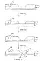
- FIG. 3 aillustrates the method steps involved in forming the organic thin film transistor shown in FIG. 2 .
- source/drain material 2 , 4is deposited on a substrate 1 (which may be opaque or transparent).
- a layer of insulating material 14is deposited over the source/drain material 1 , 4 .
- the layer of insulating material 14is patterned to form a well.
- the insulating layer 14can be formed of any insulating material which can be deposited and patterned to form a well without damaging the underlying source/drain material 2 , 4 .
- the insulating layer 14may be an organic photoresist such as a polyimide which can be readily spin coated and patterned.
- the insulating materialmay be treated with a fluorination step to alter its wettability. Alternatively, a fluorinated or fluorinated-like photoresist may be employed.
- the formation of wells (bank structures) using such materialsis well known in the art of organic light-emissive devices and will not be discussed in more detail here.
- the source and drain materialis etched to form source and drain electrodes 2 , 4 .
- Various standard metal etchesmay be used, wet or dry. These are known in the art and will not be discussed in more detail here.
- the insulating layer 14acts as an etch mask for the source/drain metal etch. As such, the method provides self-alignment of the source and drain with the overlying layers.
- the insulating layermay be exposed to an isotropic etch to thin the insulating layer and also remove insulating layer material from the source/drain edge in the well as illustrated.
- a suitable isotropic etchcan be, for example, CF 4 :0 2 , 0 2 plasma, or the like.
- organic semi-conductive material 8is deposited.
- the organic semi-conductive material 8is solution processable such that it can be deposited from solution by, for example, spin-coating or, more preferably, ink-jet printing into the wells formed by the insulating layer 14 .
- the organic semi-conductive material 8may comprise a polymer or dendrimer as these have proved to be good solution processable materials. Many such semi-conductive materials are known in the art, for example, conjugated polymers and dendrimers utilized in organic light-emissive devices.
- a dielectric layer 10is deposited over the semi-conductive layer.
- the dielectric layermay be formed of an organic or inorganic material.
- a solution processable organic materialfor example, of the same type used for the insulating layer 14 .
- a gate electrode 12is deposited over the dielectric layer 10 .
- the gate 12can be printed or deposited using other simple patterning techniques which are known in the art.
- the insulating layer 14may be utilised to reduce track leakage between lower and higher level metallization in a device such as a display (e.g. an active matrix organic light-emissive display).
- a resist stepmay be utilised to protect contact via points when performing the metal etch step in such a device to protect the contact via points during the metal etch.
- FIG. 3 billustrates the method steps involved in forming the organic thin film transistor shown in FIG. 2 in an alternative method to that of FIG. 3 a.
- the source and drain materialis etched to form source and drain electrodes 2 , 4 as shown in step 2 .
- a layer of insulating positive photoresist material 14is deposited over the patterned source and drain electrodes, and in step 4 the photoresist is pattered by exposure through transparent substrate 1 .
- the source and drain electrodes 2 , 4serve as self-aligned masks for patterning of the photoresist to leave patterned layer 14 after development of the resist.
- FIG. 4illustrates additional method steps involved in protecting via contact points.
- a resist 22is deposited in a via 20 prior to etching of the source/drain material 2 , 4 in step 4 b .
- the remaining layers of the transistorcan then be deposited in step 4 c as described previously with reference to FIG. 3 .
- Contact material 24is deposited in the via 20 to form a contact via point.
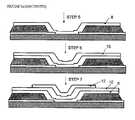
- FIG. 5illustrates formation of a well in the dielectric layer of a bottom-gate device into which the organic semiconducting material may be printed.
- the substrateis initially prepared by formation of a gate electrode 12 , a thick dielectric layer 10 ( ⁇ 1-5 ⁇ m), which could be made of polymer or inorganic materials such as SiO 2 .
- Source and drain contacts 2 , 4are then deposited (this is a bottom gate, bottom contact transistor architecture).
- the dielectric layer 10is then etched back in a controlled way in Step 1 , with the source-drain contacts 2 , 4 acting as a self-aligned mask for the etch.
- Thiscan be carried out with either a dry or wet etching technique, as long as the etching can be controlled so that it does not completely etch through the dielectric layer.
- any damage to the dielectric surface caused by the etching stepmay be repaired by, for example, deposition of a self-assembled monolayer 14 onto the exposed dielectric surface.
- the organic thin film transistoris then completed by deposition of the organic semi-conductive layer 8 as illustrated in Step 3 by printing, preferably by inkjet printing.
- the OTFT of FIG. 5comprises a thin region of dielectric material disposed in the channel region while thick regions of dielectric material are provided under the source and drain. These thick regions of dielectric material isolate the peripheral areas of the gate electrode from the source and drain so as to minimise parasitic capacitance and gate leakage to the source and drain.
- the thick regions of dielectric materialalso serve to form a well in which the organic semi-conductive material is deposited. If the well is made very deep, the conductive path length between the source and drain may be increased. This is because the charge carriers in the organic semi-conductor tend to be transported in a region of the channel close to the dielectric. Accordingly, the charge carriers may travel from the source down into the base of the well, across the channel region, and then back up to the drain. In this case, if a deep well is desired, in order to reduce the conductive path length between the source and drain, the sides of the well may be metallised.
- the substratemay be rigid or flexible.
- Rigid substratesmay be selected from glass or silicon and flexible substrates may comprise thin glass or plastics such as poly(ethylene terephthalate) (PET), poly(ethylene-naphthalate) PEN, polycarbonate and polyimide.
- PETpoly(ethylene terephthalate)
- PENpoly(ethylene-naphthalate) PEN
- polycarbonatepolyimide
- the organic semiconductive materialmay be made solution processable through the use of a suitable solvent.
- suitable solventsinclude mono- or poly-alkylbenzenes such as toluene and xylene; tetralin; and chloroform.
- Preferred solution deposition techniquesinclude spin coating and ink jet printing. Other solution deposition techniques include dip-coating; roll printing; and screen printing. In cases where a solution is dispensed from a nozzle, the printing process may be either continuous or discontinuous. For example, in a continuous process a continuous strip of organic semiconductive material may be dispensed from a nozzle, whereas discontinuous drops are dispensed from a nozzle in a discontinuous printing process.
- Preferred organic semiconductor materialsinclude small molecules such as optionally substituted pentacene; optionally substituted polymers such as polyarylenes, in particular polyfluorenes and polythiophenes; and oligomers. Blends of materials, including blends of different material types (e.g. a polymer and small molecule blend) may be used.
- the source and drain electrodescomprise a high workfunction material, preferably a metal, with a workfunction of greater than 3.5 eV, for example gold, platinum, palladium, molybdenum, tungsten, or chromium. More preferably, the metal has a workfunction in the range of from 4.5 to 5.5 eV. Other suitable compounds, alloys and oxides such as molybdenum trioxide and indium tin oxide may also be used.
- the source and drain electrodesmay be deposited by thermal evaporation and patterned using standard photolithography and lift off techniques as are known in the art.
- conductive polymersmay be deposited as the source and drain electrodes.
- An example of such a conductive polymersis poly(ethylene dioxythiophene) (PEDOT) although other conductive polymers are known in the art.
- PEDOTpoly(ethylene dioxythiophene)
- Such conductive polymersmay be deposited from solution using, for example, spin coating or ink jet printing techniques and other solution deposition techniques discussed above.
- the source and drain electrodescomprise a material, for example a metal having a workfunction of less than 3.5 eV such as calcium or barium or a thin layer of metal compound, in particular an oxide or fluoride of an alkali or alkali earth metal for example lithium fluoride, barium fluoride and barium oxide.
- a metal having a workfunction of less than 3.5 eVsuch as calcium or barium or a thin layer of metal compound, in particular an oxide or fluoride of an alkali or alkali earth metal for example lithium fluoride, barium fluoride and barium oxide.
- conductive polymersmay be deposited as the source and drain electrodes.
- the source and drain electrodesare preferably formed from the same material for ease of manufacture. However, it will be appreciated that the source and drain electrodes may be formed of different materials for optimisation of charge injection and extraction respectively.
- the length of the channel defined between the source and drain electrodesmay be up to 500 microns, but preferably the length is less than 200 microns, more preferably less than 100 microns, most preferably less than 20 microns.
- the gate electrode 4can be selected from a wide range of conducting materials for example a metal (e.g. gold) or metal compound (e.g. indium tin oxide).
- conductive polymersmay be deposited as the gate electrode 4 .
- Such conductive polymersmay be deposited from solution using, for example, spin coating or ink jet printing techniques and other solution deposition techniques discussed above
- Thicknesses of the gate electrode, source and drain electrodesmay be in the region of 5-200 nm, although typically 50 nm as measured by Atomic Force Microscopy (AFM), for example.
- AFMAtomic Force Microscopy
- the insulating layercomprises a dielectric material selected from insulating materials having a high resistivity.
- the dielectric constant, k, of the dielectricis typically around 2-3 although materials with a high value of k are desirable because the capacitance that is achievable for an OTFT is directly proportional to k, and the drain current ID is directly proportional to the capacitance.
- OTFTs with thin dielectric layers in the channel regionare preferred.
- the dielectric materialmay be organic or inorganic.
- Preferred inorganic materialsinclude Sio2, SiNx and spin-on-glass (SOG).
- Preferred organic materialsare generally polymers and include insulating polymers such as poly vinylalcohol (PVA), polyvinylpyrrolidine (PVP), acrylates such as polymethylmethacrylate (PMMA) and benzocyclobutanes (BCBs) available from Dow Corning.
- the insulating layermay be formed from a blend of materials or comprise a multi-layered structure.
- the dielectric materialmay be deposited by thermal evaporation, vacuum processing or lamination techniques as are known in the art. Alternatively, the dielectric material may be deposited from solution using, for example, spin coating or ink jet printing techniques and other solution deposition techniques discussed above.
- the dielectric materialis deposited from solution onto the organic semiconductor, it should not result in dissolution of the organic semiconductor. Likewise, the dielectric material should not be dissolved if the organic semiconductor is deposited onto it from solution. Techniques to avoid such dissolution include: use of orthogonal solvents, that is use of a solvent for deposition of the uppermost layer that does not dissolve the underlying layer; and crosslinking of the underlying layer.
- the thickness of the insulating layeris preferably less than 2 micrometres, more preferably less than 500 nm.
- a self assembled monolayermay be deposited on the gate, source or drain electrodes, substrate, insulating layer and organic semiconductor material to promote crystallity, reduce contact resistance, repair surface characteristics and promote adhesion where required.
- the dielectric surface in the channel regionmay be provided with a monolayer comprising a binding region and an organic region to improve device performance, e.g. by improving the organic semiconductor's morphology (in particular polymer alignment and crystallinity) and covering charge traps, in particular for a high k dielectric surface.
- Exemplary materials for such a monolayerinclude chloro- or alkoxy-silanes with long alkyl chains, e.g. octadecyltrichlorosilane.
- OTFTsaccording to embodiments of the present invention have a wide range of possible applications.
- One such applicationis to drive pixels in an optical device, preferably an organic optical device.
- optical devicesinclude photoresponsive devices, in particular photodetectors, and light-emissive devices, in particular organic light emitting devices.
- OTFTsare particularly suited for use with active matrix organic light emitting devices, e.g. for use in display applications.
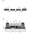
- FIG. 5illustrates an organic light-emitting device (OLED) pixel according to the invention.
- the OTFTcomprises layers 2 - 14 described above.
- the OLEDcomprises anode 51 , cathode 53 and an electroluminescent layer 52 provided between the anode and cathode. Further layers may be located between the anode and cathode, such as charge transporting, charge injecting or charge blocking layers.
- the active area of the OLEDis defined by a well formed by patterning a layer of insulating photoresist 54 .
- the OLEDis constructed on a planarisation layer 55 (also known as a passivation layer) that is deposited over the OTFT.
- Exemplary materials for use in forming the passivation layerare BCBs and parylenes.
- the anode 51 of the OLEDis electrically connected to the drain electrode of the organic thin film transistor by a conductive via 56 passing through passivation layer 55 and insulating layer 14 .
- pixel circuitscomprising an OTFT and an optically active pixel area (e.g. light emitting or light sensing pixel area) may comprise further elements.
- the OLED pixel circuit of FIG. 5will typically comprise least one further transistor in addition to the driving transistor shown, and at least one capacitor.
Landscapes
- Engineering & Computer Science (AREA)
- Manufacturing & Machinery (AREA)
- Thin Film Transistor (AREA)
Abstract
Description
Claims (16)
Applications Claiming Priority (3)
| Application Number | Priority Date | Filing Date | Title |
|---|---|---|---|
| GB0706652AGB2448174B (en) | 2007-04-04 | 2007-04-04 | Organic thin film transistors |
| GB0706652.5 | 2007-04-04 | ||
| PCT/EP2008/054040WO2008122575A1 (en) | 2007-04-04 | 2008-04-03 | Organic thin film transistors |
Publications (2)
| Publication Number | Publication Date |
|---|---|
| US20100051922A1 US20100051922A1 (en) | 2010-03-04 |
| US8450142B2true US8450142B2 (en) | 2013-05-28 |
Family
ID=38090909
Family Applications (1)
| Application Number | Title | Priority Date | Filing Date |
|---|---|---|---|
| US12/532,629Expired - Fee RelatedUS8450142B2 (en) | 2007-04-04 | 2008-04-03 | Organic thin film transistors |
Country Status (7)
| Country | Link |
|---|---|
| US (1) | US8450142B2 (en) |
| EP (1) | EP2122706B1 (en) |
| JP (1) | JP5638944B2 (en) |
| KR (1) | KR101467507B1 (en) |
| CN (1) | CN101983439B (en) |
| GB (1) | GB2448174B (en) |
| WO (1) | WO2008122575A1 (en) |
Cited By (4)
| Publication number | Priority date | Publication date | Assignee | Title |
|---|---|---|---|---|
| US9583722B2 (en) | 2014-07-04 | 2017-02-28 | Boe Technology Group Co., Ltd. | Organic thin film transistor and preparation method thereof, array substrate and preparation method thereof, and display device |
| US9991265B2 (en) | 2009-12-25 | 2018-06-05 | Semiconductor Energy Laboratory Co., Ltd. | Semiconductor device |
| US10373983B2 (en) | 2016-08-03 | 2019-08-06 | Semiconductor Energy Laboratory Co., Ltd. | Display device and electronic device |
| EP3915156A1 (en)* | 2019-01-23 | 2021-12-01 | Technische Universität Dresden | Organic thin film transistor and method for producing same |
Families Citing this family (24)
| Publication number | Priority date | Publication date | Assignee | Title |
|---|---|---|---|---|
| US8211782B2 (en)* | 2009-10-23 | 2012-07-03 | Palo Alto Research Center Incorporated | Printed material constrained by well structures |
| WO2011088343A2 (en)* | 2010-01-17 | 2011-07-21 | Polyera Corporation | Dielectric materials and methods of preparation and use thereof |
| US8603922B2 (en)* | 2010-01-27 | 2013-12-10 | Creator Technology B.V. | Semiconductor device, display, electronic apparatus and method of manufacturing a semiconductor device |
| KR101088056B1 (en) | 2010-02-05 | 2011-11-29 | 연세대학교 산학협력단 | Organic Field Effect Transistors and Manufacturing Method Thereof |
| US8436403B2 (en)* | 2010-02-05 | 2013-05-07 | Semiconductor Energy Laboratory Co., Ltd. | Semiconductor device including transistor provided with sidewall and electronic appliance |
| CN102844847B (en)* | 2010-04-16 | 2015-09-23 | 株式会社半导体能源研究所 | The manufacture method of deposition process and semiconductor device |
| WO2012014786A1 (en)* | 2010-07-30 | 2012-02-02 | Semiconductor Energy Laboratory Co., Ltd. | Semicondcutor device and manufacturing method thereof |
| US8704230B2 (en) | 2010-08-26 | 2014-04-22 | Semiconductor Energy Laboratory Co., Ltd. | Semiconductor device and manufacturing method thereof |
| US8664097B2 (en) | 2010-09-13 | 2014-03-04 | Semiconductor Energy Laboratory Co., Ltd. | Manufacturing method of semiconductor device |
| KR20140019341A (en)* | 2011-03-03 | 2014-02-14 | 올싸거널 인코포레이티드 | Process for patterning materials in thin-film devices |
| US8569121B2 (en)* | 2011-11-01 | 2013-10-29 | International Business Machines Corporation | Graphene and nanotube/nanowire transistor with a self-aligned gate structure on transparent substrates and method of making same |
| CN202332973U (en) | 2011-11-23 | 2012-07-11 | 京东方科技集团股份有限公司 | Organic thin film transistor, organic thin film transistor array substrate and display device |
| GB2521139B (en)* | 2013-12-10 | 2017-11-08 | Flexenable Ltd | Reducing undesirable capacitive coupling in transistor devices |
| WO2016085063A1 (en)* | 2014-11-24 | 2016-06-02 | 서울대학교 산학협력단 | Method for manufacturing high-density organic memory device |
| CN105261652B (en)* | 2015-07-10 | 2019-08-13 | 广州奥翼电子科技股份有限公司 | Organic semiconductor thin film transistor and its manufacturing method and display device and backboard |
| CN105140261B (en) | 2015-07-28 | 2018-09-11 | 京东方科技集团股份有限公司 | Organic Thin Film Transistors and preparation method thereof, array substrate and display device |
| US9842883B2 (en)* | 2016-01-28 | 2017-12-12 | Shenzhen China Star Optoelectronics Technology Co., Ltd. | Flexible array substrate structure and manufacturing method for the same |
| CN105655295A (en)* | 2016-01-28 | 2016-06-08 | 京东方科技集团股份有限公司 | Array substrate and manufacturing method thereof as well as display device |
| CN105529337B (en)* | 2016-01-28 | 2018-12-11 | 深圳市华星光电技术有限公司 | Flexible array substrate structure and its manufacturing method |
| CN105467708B (en)* | 2016-02-03 | 2021-04-20 | 京东方科技集团股份有限公司 | A writing board, electronic writing equipment and production method |
| TWI759147B (en) | 2016-08-12 | 2022-03-21 | 美商因普利亞公司 | Methods of reducing metal residue in edge bead region from metal-containing resists |
| US20190326368A1 (en)* | 2018-04-23 | 2019-10-24 | Shenzhen China Star Optoelectronics Semiconductor Display Technology Co., Ltd. | Oled component, method for manufacturing the same and oled display |
| CN109894162B (en)* | 2019-03-11 | 2021-06-11 | 太原理工大学 | A PEDOT-based: micro-fluidic chip of PSS electrochemical transistor and preparation method thereof |
| GB2590427B (en)* | 2019-12-17 | 2024-08-28 | Flexenable Tech Limited | Semiconductor devices |
Citations (11)
| Publication number | Priority date | Publication date | Assignee | Title |
|---|---|---|---|---|
| US6300988B1 (en)* | 1999-03-16 | 2001-10-09 | Hitachi, Ltd. | Liquid crystal display apparatus having patterned insulating layer formed over a substrate except for a region on the gate electrode |
| EP1263062A2 (en) | 2001-06-01 | 2002-12-04 | Sel Semiconductor Energy Laboratory Co., Ltd. | Organic semiconductor device and process of manufacturing the same |
| JP2004055649A (en) | 2002-07-17 | 2004-02-19 | Konica Minolta Holdings Inc | Organic thin film transistor and method of manufacturing the same |
| JP2005108949A (en) | 2003-09-29 | 2005-04-21 | Matsushita Electric Ind Co Ltd | Field effect transistor and manufacturing method thereof |
| US20060060855A1 (en)* | 2004-09-20 | 2006-03-23 | Hun-Jung Lee | Organic thin film transistor and flat panel display including the same |
| US20060220022A1 (en)* | 2005-03-30 | 2006-10-05 | Seiko Epson Corporation | Semiconductor device, electronic apparatus, method of manufacturing semiconductor device, and method of manufacturing electronic apparatus |
| CN1905233A (en) | 2005-07-27 | 2007-01-31 | 三星电子株式会社 | Thin film transistor substrate and method of making the same |
| US20070252207A1 (en)* | 2006-04-27 | 2007-11-01 | Samsung Electronics Co. Ltd. | Thin film transistor and method of fabricating the same |
| JP2008109116A (en) | 2006-09-26 | 2008-05-08 | Dainippon Printing Co Ltd | Organic semiconductor device, organic semiconductor device manufacturing method, organic transistor array, and display |
| US20080128685A1 (en) | 2006-09-26 | 2008-06-05 | Hiroyuki Honda | Organic semiconductor device, manufacturing method of same, organic transistor array, and display |
| US7919365B2 (en)* | 2006-04-18 | 2011-04-05 | Samsung Electronics Co., Ltd. | Fabrication methods of a ZnO thin film structure and a ZnO thin film transistor, and a ZnO thin film structure and a ZnO thin film transistor |
Family Cites Families (17)
| Publication number | Priority date | Publication date | Assignee | Title |
|---|---|---|---|---|
| JP3325072B2 (en)* | 1992-03-02 | 2002-09-17 | モトローラ・インコーポレイテッド | Semiconductor memory device |
| JP3136193B2 (en)* | 1992-06-05 | 2001-02-19 | 富士通株式会社 | Thin film transistor and method of manufacturing the same |
| JP3181692B2 (en)* | 1992-06-26 | 2001-07-03 | 富士通株式会社 | Thin film transistor and method of manufacturing the same |
| JP3842852B2 (en)* | 1995-11-27 | 2006-11-08 | 株式会社半導体エネルギー研究所 | Method for manufacturing semiconductor device |
| JP4630420B2 (en)* | 2000-05-23 | 2011-02-09 | ティーピーオー ホンコン ホールディング リミテッド | Pattern formation method |
| US6740900B2 (en)* | 2002-02-27 | 2004-05-25 | Konica Corporation | Organic thin-film transistor and manufacturing method for the same |
| JP4275346B2 (en)* | 2002-03-08 | 2009-06-10 | 株式会社半導体エネルギー研究所 | Method for manufacturing semiconductor device |
| CN1186822C (en)* | 2002-09-23 | 2005-01-26 | 中国科学院长春应用化学研究所 | Organic film transistor and preparing method |
| JP2005072053A (en)* | 2003-08-27 | 2005-03-17 | Sharp Corp | Organic semiconductor device and manufacturing method thereof |
| JP4610173B2 (en)* | 2003-10-10 | 2011-01-12 | 株式会社半導体エネルギー研究所 | Method for manufacturing thin film transistor |
| JP2005286320A (en)* | 2004-03-04 | 2005-10-13 | Semiconductor Energy Lab Co Ltd | Pattern forming method, thin film transistor, display device, forming method thereof, and television device |
| JP2008520086A (en)* | 2004-11-09 | 2008-06-12 | コーニンクレッカ フィリップス エレクトロニクス エヌ ヴィ | Self-aligned process for manufacturing organic transistors |
| JP2006351844A (en)* | 2005-06-16 | 2006-12-28 | Mitsubishi Electric Corp | Electro-optic display device and manufacturing method thereof |
| KR20070009013A (en)* | 2005-07-14 | 2007-01-18 | 삼성전자주식회사 | Flat panel display and flat panel display manufacturing method |
| WO2007114254A1 (en)* | 2006-03-29 | 2007-10-11 | Pioneer Corporation | Organic thin film transistor and method for manufacturing same |
| KR101279296B1 (en)* | 2006-04-17 | 2013-06-26 | 엘지디스플레이 주식회사 | Organic semiconductor sturcture and methodd of manufacturing the same organic thin film transistor using the organic semiconductor sturcture and method of manufacturing the organic thin film transistor and display apparatus using the same |
| JP3905915B2 (en)* | 2006-05-08 | 2007-04-18 | クラリオン株式会社 | Disk unit |
- 2007
- 2007-04-04GBGB0706652Apatent/GB2448174B/ennot_activeExpired - Fee Related
- 2008
- 2008-04-03WOPCT/EP2008/054040patent/WO2008122575A1/ennot_activeCeased
- 2008-04-03CNCN2008800105631Apatent/CN101983439B/ennot_activeExpired - Fee Related
- 2008-04-03JPJP2010501516Apatent/JP5638944B2/ennot_activeExpired - Fee Related
- 2008-04-03KRKR1020097021703Apatent/KR101467507B1/ennot_activeExpired - Fee Related
- 2008-04-03USUS12/532,629patent/US8450142B2/ennot_activeExpired - Fee Related
- 2008-04-03EPEP08735782Apatent/EP2122706B1/ennot_activeNot-in-force
Patent Citations (16)
| Publication number | Priority date | Publication date | Assignee | Title |
|---|---|---|---|---|
| US6300988B1 (en)* | 1999-03-16 | 2001-10-09 | Hitachi, Ltd. | Liquid crystal display apparatus having patterned insulating layer formed over a substrate except for a region on the gate electrode |
| EP1263062A2 (en) | 2001-06-01 | 2002-12-04 | Sel Semiconductor Energy Laboratory Co., Ltd. | Organic semiconductor device and process of manufacturing the same |
| US20020179901A1 (en)* | 2001-06-01 | 2002-12-05 | Semiconductor Energy Laboratory Co., Ltd. | Organic semiconductor device and process of manufacturing the same |
| US6635508B2 (en)* | 2001-06-01 | 2003-10-21 | Semiconductor Energy Laboratory Co., Ltd. | Organic semiconductor device and process of manufacturing the same |
| JP2004055649A (en) | 2002-07-17 | 2004-02-19 | Konica Minolta Holdings Inc | Organic thin film transistor and method of manufacturing the same |
| JP2005108949A (en) | 2003-09-29 | 2005-04-21 | Matsushita Electric Ind Co Ltd | Field effect transistor and manufacturing method thereof |
| US7288818B2 (en)* | 2004-09-20 | 2007-10-30 | Samsung Sdi Co., Ltd. | Organic thin film transistor with low gate overlap capacitance and flat panel display including the same |
| US20060060855A1 (en)* | 2004-09-20 | 2006-03-23 | Hun-Jung Lee | Organic thin film transistor and flat panel display including the same |
| US20060220022A1 (en)* | 2005-03-30 | 2006-10-05 | Seiko Epson Corporation | Semiconductor device, electronic apparatus, method of manufacturing semiconductor device, and method of manufacturing electronic apparatus |
| CN1905233A (en) | 2005-07-27 | 2007-01-31 | 三星电子株式会社 | Thin film transistor substrate and method of making the same |
| JP2007036259A (en) | 2005-07-27 | 2007-02-08 | Samsung Electronics Co Ltd | Thin film transistor substrate and manufacturing method thereof |
| US20070023837A1 (en)* | 2005-07-27 | 2007-02-01 | Samsung Electronics Co., Ltd. | Thin film transistor substrate and method of making the same |
| US7919365B2 (en)* | 2006-04-18 | 2011-04-05 | Samsung Electronics Co., Ltd. | Fabrication methods of a ZnO thin film structure and a ZnO thin film transistor, and a ZnO thin film structure and a ZnO thin film transistor |
| US20070252207A1 (en)* | 2006-04-27 | 2007-11-01 | Samsung Electronics Co. Ltd. | Thin film transistor and method of fabricating the same |
| JP2008109116A (en) | 2006-09-26 | 2008-05-08 | Dainippon Printing Co Ltd | Organic semiconductor device, organic semiconductor device manufacturing method, organic transistor array, and display |
| US20080128685A1 (en) | 2006-09-26 | 2008-06-05 | Hiroyuki Honda | Organic semiconductor device, manufacturing method of same, organic transistor array, and display |
Non-Patent Citations (5)
| Title |
|---|
| British Search and Examination Resort for GB 0706652.5 dated May 15, 2009. |
| Iba et al., "Control of threshold voltage of organic field-effect transistors with double-gate structures," Applied Physics Letters, AIP, Am. In. Phys., 87:23509-1-023509-3 (2005). |
| International Search Resort and Written Opinion for PCT/EP2008/054040 dated Jul. 15, 2008. |
| Office Action for corresponding Chinese Application No. 20088001563.1, dated Oct. 27, 2011. |
| Partial English translation of Office Action for corresponding Japanese Patent Application No. 2010-501516, dated Feb. 19, 2013. |
Cited By (13)
| Publication number | Priority date | Publication date | Assignee | Title |
|---|---|---|---|---|
| US11825665B2 (en) | 2009-12-25 | 2023-11-21 | Semiconductor Energy Laboratory Co., Ltd. | Semiconductor device |
| US9991265B2 (en) | 2009-12-25 | 2018-06-05 | Semiconductor Energy Laboratory Co., Ltd. | Semiconductor device |
| US10553589B2 (en) | 2009-12-25 | 2020-02-04 | Semiconductor Energy Laboratory Co., Ltd. | Semiconductor device |
| US11456296B2 (en) | 2009-12-25 | 2022-09-27 | Semiconductor Energy Laboratory Co., Ltd. | Semiconductor device |
| US12283599B2 (en) | 2009-12-25 | 2025-04-22 | Semiconductor Energy Laboratory Co., Ltd. | Semiconductor device |
| US9583722B2 (en) | 2014-07-04 | 2017-02-28 | Boe Technology Group Co., Ltd. | Organic thin film transistor and preparation method thereof, array substrate and preparation method thereof, and display device |
| US10373983B2 (en) | 2016-08-03 | 2019-08-06 | Semiconductor Energy Laboratory Co., Ltd. | Display device and electronic device |
| US10700098B2 (en) | 2016-08-03 | 2020-06-30 | Semiconductor Energy Laboratory Co., Ltd. | Display device and electronic device |
| US11404447B2 (en) | 2016-08-03 | 2022-08-02 | Semiconductor Energy Laboratory Co., Ltd. | Display device and electronic device |
| US11676971B2 (en) | 2016-08-03 | 2023-06-13 | Semiconductor Energy Laboratory Co., Ltd. | Display device and electronic device |
| US12027528B2 (en) | 2016-08-03 | 2024-07-02 | Semiconductor Energy Laboratory Co., Ltd. | Display device and electronic device |
| EP3915156A1 (en)* | 2019-01-23 | 2021-12-01 | Technische Universität Dresden | Organic thin film transistor and method for producing same |
| US12317665B2 (en) | 2019-01-23 | 2025-05-27 | Flexora Gmbh | Organic thin film transistor and method for producing same |
Also Published As
| Publication number | Publication date |
|---|---|
| GB0706652D0 (en) | 2007-05-16 |
| HK1134583A1 (en) | 2010-04-30 |
| GB2448174B (en) | 2009-12-09 |
| JP2010524217A (en) | 2010-07-15 |
| WO2008122575A1 (en) | 2008-10-16 |
| US20100051922A1 (en) | 2010-03-04 |
| EP2122706A1 (en) | 2009-11-25 |
| CN101983439B (en) | 2012-12-12 |
| KR20100015664A (en) | 2010-02-12 |
| CN101983439A (en) | 2011-03-02 |
| EP2122706B1 (en) | 2012-11-14 |
| GB2448174A (en) | 2008-10-08 |
| WO2008122575A9 (en) | 2010-01-21 |
| KR101467507B1 (en) | 2014-12-01 |
| JP5638944B2 (en) | 2014-12-10 |
Similar Documents
| Publication | Publication Date | Title |
|---|---|---|
| US8450142B2 (en) | Organic thin film transistors | |
| US8089065B2 (en) | Organic thin film transistors | |
| US8697504B2 (en) | Organic thin film transistors, active matrix organic optical devices and methods of making the same | |
| US20100264408A1 (en) | Organic Thin Film Transistors, Active Matrix Organic Optical Devices and Methods of Making the Same | |
| US8013328B2 (en) | Active matrix optical device | |
| KR101532759B1 (en) | Organic thin film transistors | |
| US20110053314A1 (en) | Method of Fabricating Top Gate Organic Semiconductor Transistors | |
| US8546179B2 (en) | Method of fabricating a self-aligned top-gate organic transistor | |
| HK1134583B (en) | Method of forming organic thin film transistors |
Legal Events
| Date | Code | Title | Description |
|---|---|---|---|
| AS | Assignment | Owner name:CAMBRIDGE DISPLAY TECHNOLOGY LTD.,UNITED KINGDOM Free format text:ASSIGNMENT OF ASSIGNORS INTEREST;ASSIGNORS:HOTTA, SADAYOSHI;BURROUGHES, JEREMY HENLEY;WHITING, GREGORY LEWIS;SIGNING DATES FROM 20090924 TO 20090930;REEL/FRAME:023463/0684 Owner name:PANASONIC CORPORATION,JAPAN Free format text:ASSIGNMENT OF ASSIGNORS INTEREST;ASSIGNORS:HOTTA, SADAYOSHI;BURROUGHES, JEREMY HENLEY;WHITING, GREGORY LEWIS;SIGNING DATES FROM 20090924 TO 20090930;REEL/FRAME:023463/0684 Owner name:PANASONIC CORPORATION, JAPAN Free format text:ASSIGNMENT OF ASSIGNORS INTEREST;ASSIGNORS:HOTTA, SADAYOSHI;BURROUGHES, JEREMY HENLEY;WHITING, GREGORY LEWIS;SIGNING DATES FROM 20090924 TO 20090930;REEL/FRAME:023463/0684 Owner name:CAMBRIDGE DISPLAY TECHNOLOGY LTD., UNITED KINGDOM Free format text:ASSIGNMENT OF ASSIGNORS INTEREST;ASSIGNORS:HOTTA, SADAYOSHI;BURROUGHES, JEREMY HENLEY;WHITING, GREGORY LEWIS;SIGNING DATES FROM 20090924 TO 20090930;REEL/FRAME:023463/0684 | |
| STCF | Information on status: patent grant | Free format text:PATENTED CASE | |
| FPAY | Fee payment | Year of fee payment:4 | |
| FEPP | Fee payment procedure | Free format text:MAINTENANCE FEE REMINDER MAILED (ORIGINAL EVENT CODE: REM.); ENTITY STATUS OF PATENT OWNER: LARGE ENTITY | |
| LAPS | Lapse for failure to pay maintenance fees | Free format text:PATENT EXPIRED FOR FAILURE TO PAY MAINTENANCE FEES (ORIGINAL EVENT CODE: EXP.); ENTITY STATUS OF PATENT OWNER: LARGE ENTITY | |
| STCH | Information on status: patent discontinuation | Free format text:PATENT EXPIRED DUE TO NONPAYMENT OF MAINTENANCE FEES UNDER 37 CFR 1.362 | |
| FP | Lapsed due to failure to pay maintenance fee | Effective date:20210528 |