US8449128B2 - System and method for a lens and phosphor layer - Google Patents
System and method for a lens and phosphor layerDownload PDFInfo
- Publication number
- US8449128B2 US8449128B2US12/646,570US64657009AUS8449128B2US 8449128 B2US8449128 B2US 8449128B2US 64657009 AUS64657009 AUS 64657009AUS 8449128 B2US8449128 B2US 8449128B2
- Authority
- US
- United States
- Prior art keywords
- lens
- led
- cavity
- phosphor
- light
- Prior art date
- Legal status (The legal status is an assumption and is not a legal conclusion. Google has not performed a legal analysis and makes no representation as to the accuracy of the status listed.)
- Expired - Fee Related, expires
Links
Images


Classifications
- G—PHYSICS
- G02—OPTICS
- G02B—OPTICAL ELEMENTS, SYSTEMS OR APPARATUS
- G02B19/00—Condensers, e.g. light collectors or similar non-imaging optics
- G02B19/0033—Condensers, e.g. light collectors or similar non-imaging optics characterised by the use
- G02B19/0047—Condensers, e.g. light collectors or similar non-imaging optics characterised by the use for use with a light source
- G02B19/0061—Condensers, e.g. light collectors or similar non-imaging optics characterised by the use for use with a light source the light source comprising a LED
- G02B19/0066—Condensers, e.g. light collectors or similar non-imaging optics characterised by the use for use with a light source the light source comprising a LED in the form of an LED array
- G—PHYSICS
- G02—OPTICS
- G02B—OPTICAL ELEMENTS, SYSTEMS OR APPARATUS
- G02B19/00—Condensers, e.g. light collectors or similar non-imaging optics
- G02B19/0004—Condensers, e.g. light collectors or similar non-imaging optics characterised by the optical means employed
- G02B19/0028—Condensers, e.g. light collectors or similar non-imaging optics characterised by the optical means employed refractive and reflective surfaces, e.g. non-imaging catadioptric systems
- G—PHYSICS
- G02—OPTICS
- G02B—OPTICAL ELEMENTS, SYSTEMS OR APPARATUS
- G02B19/00—Condensers, e.g. light collectors or similar non-imaging optics
- G02B19/0033—Condensers, e.g. light collectors or similar non-imaging optics characterised by the use
- G02B19/0047—Condensers, e.g. light collectors or similar non-imaging optics characterised by the use for use with a light source
- G02B19/0061—Condensers, e.g. light collectors or similar non-imaging optics characterised by the use for use with a light source the light source comprising a LED
- F—MECHANICAL ENGINEERING; LIGHTING; HEATING; WEAPONS; BLASTING
- F21—LIGHTING
- F21K—NON-ELECTRIC LIGHT SOURCES USING LUMINESCENCE; LIGHT SOURCES USING ELECTROCHEMILUMINESCENCE; LIGHT SOURCES USING CHARGES OF COMBUSTIBLE MATERIAL; LIGHT SOURCES USING SEMICONDUCTOR DEVICES AS LIGHT-GENERATING ELEMENTS; LIGHT SOURCES NOT OTHERWISE PROVIDED FOR
- F21K9/00—Light sources using semiconductor devices as light-generating elements, e.g. using light-emitting diodes [LED] or lasers
- F21K9/60—Optical arrangements integrated in the light source, e.g. for improving the colour rendering index or the light extraction
- F21K9/64—Optical arrangements integrated in the light source, e.g. for improving the colour rendering index or the light extraction using wavelength conversion means distinct or spaced from the light-generating element, e.g. a remote phosphor layer
- H—ELECTRICITY
- H10—SEMICONDUCTOR DEVICES; ELECTRIC SOLID-STATE DEVICES NOT OTHERWISE PROVIDED FOR
- H10H—INORGANIC LIGHT-EMITTING SEMICONDUCTOR DEVICES HAVING POTENTIAL BARRIERS
- H10H20/00—Individual inorganic light-emitting semiconductor devices having potential barriers, e.g. light-emitting diodes [LED]
- H10H20/80—Constructional details
- H10H20/85—Packages
- H10H20/851—Wavelength conversion means
- H10H20/8515—Wavelength conversion means not being in contact with the bodies
Definitions
- the present disclosurerelates generally to optical systems. More particularly, the present disclosure relates to systems and methods for using phosphors or other photon converting materials in conjunction with a light source and lens.
- Phosphorsare lambertian emitters, emitting light in all directions.
- phosphoris applied on the LED chip, in a silicone matrix in proximity to the LED or to the outside of an LED dome or other LED packaging.
- a domemay be applied to an LED chip coated with phosphor to control the light beam angle (shape) from lambertian to a very narrow spot.
- Such devicesrange from hemispherical lenses to T-5 mm (T 13 ⁇ 4) aspheres.
- One conventional system for producing white light LEDsfor example, is constructed with pump blue/UV LED chips and a proximate mixture of phosphor in a binding matrix such as silicone.
- the term “goop in a cup”is used to describe LEDs with flat or very nearly flat phosphor and silicone mixture over a blue pump.
- phosphoris applied away from the chip on the outside of a dome or inside of a hemispherical shell to increase converting efficiency.
- an additional lensmay be needed to control light beam shape.
- the GE VIO®employs the remote phosphor solution.
- U.S. Pat. No. 6,614,179discloses a light emitting device with blue light emitting diode and phosphor components.
- U.S. Pat. Nos. 5,998,925, 6,069,440, and 6,608,332disclose white light emitting devices, each having a nitride compound semiconductor and a phosphor containing yttrium-aluminum-garnet (YAG) elements.
- the nitride compound semiconductoris used as a light emitting layer.
- the phosphorabsorbs a part of light emitted by the light emitting layer and emits light of a wavelength different from that of the absorbed light.
- U.S. Pat. No. 6,737,681discloses chip placement designs for white light packages.
- One exampleincludes a fluorescent member having a curved surface or concave arc that extends from the height of the bottom of a case obliquely upward in a shape that continues along substantially the entire circumference of an oval or elongated round shape. It reflects the light emitted from the side faces of a semiconductor light emitting element to more efficiently utilize part of the light emitted from the semiconductor light emitting element and most of the light emitted from the side faces.
- 6,924,596discloses a color conversion type light emitting apparatus having a light emitting device and a color converting member formed from an epoxy resin containing a photoluminescence fluorescent substance and directly coating the light emitting device.
- U.S. Pat. Nos. 7,091,656 and 7,247,257disclose light emitting devices that use a mixture of at least two phosphors for more complete color rendering.
- U.S. Pat. No. 7,071,616discloses a light source having a blue LED, an optical guide plate having a planar main surface and an edge face receiving injection of the light from the blue LED and a coating material of transparent resin or glass containing fluorescent materials positioned between the blue LED and the optical guide plate. The optical guide plate is used for the final light mixing.
- Nos. 7,026,756, 7,126,274, 7,329,988, 7,362,048disclose light emitting devices with blue light LED and phosphor components, including the emission spectra and package designs for display backlight.
- U.S. Pat. No. 6,960,878discloses an LED chip having a blue die and a phosphor and including an epoxy resin for better reliability and optical stability.
- U.S. Pat. No. 7,256,468discloses a light emitting device having a light emitting element and a metal package with a heat radiating characteristic and mechanical strength for housing the light emitting element.
- Embodiments described hereinprovide optical systems in which phosphor can down convert light prior to the light entering a lens body.
- One embodimentcan include a system comprising an LED, a lens and phosphor disposed on the lens.
- the LEDis positioned in a cavity defined by a base and one or more sidewalls.
- the phosphorsare disposed on the lens between the entrance face to the lens body and the LED so that light emitted from the LED will be incident on the phosphor and down converted before entering the lens body through the entrance face.
- the lensis positioned so that the phosphors are separated from the LED by a gap.
- the phosphorcan be disposed as a coating on the entrance face of the lens body, on a buffer layer between the phosphor and the entrance face or otherwise disposed on the lens.
- the lens bodycan be shaped to emit light with a uniform distribution in a desired half-angle. Additionally, the lens body can be shaped to conserve brightness or come within a desired percentage of conserving brightness.
- the cavitycan have sidewalls that are shaped to direct light in the cavity to the entrance face of the LED.
- the material forming the cavity sidewallscan be selected to reflect light to the entrance face.
- a reflectorcan surround the LED.
- the reflectorcan be a separate component or, according to one embodiment, can be formed by surface tension at the edges of the cavity if the cavity is filled with encapsulant.
- an optical systemcan comprise a submount, an array of LEDs mounted to the submount, a housing and a set of lenses.
- the housingcan at least partially define a set of LED cavities in cooperation with the submount.
- the housingcan also define a set of lens cavities to accommodate the lenses.
- Each lens cavitycan be open to a corresponding LED cavity.
- the lensescan be disposed in the lens cavities with each lens comprising an entrance face proximate to the opening to the corresponding LED cavity.
- a layer of phosphorscan disposed on each lens between the entrance face and the corresponding LED so that light is down converted before entering the lens body.
- the entrance face of each lensis positioned a distance from the corresponding LED so that there is a gap between the LED and the phosphors.
- Each lens cavitycan be defined by a set of sidewalls.
- the set of sidewallscan be shaped so that the lens cavity is smaller proximate to the opening to the corresponding LED cavity and larger distal from the opening of the corresponding LED cavity.
- Each lens in the set of lensescan be configured to emit light with a uniform distribution pattern in a selected half-angle.
- the set of lensescan be closely packed so that the optical system emits light in a uniform distribution pattern in the selected half-angle over a larger area than the individual lenses in the set of lenses. Additionally, each lens in the set of lenses can be shaped to conserve brightness.
- the systemcan include a cover that supports one or more lenses in corresponding lens cavities.
- the cover and one or more lensescan be formed of a single piece of material.
- the phosphor layer disposed on each lenscan be selected so that different lenses in the set of lenses emit different colors of light.
- the phosphor layer disposed on each lensis selected so that the optical system forms one or more white light units.
- One advantage provided by embodiments described hereinis that phosphor is removed from the LED chip. Heating of the LED chip is therefore reduced or prevented.
- phosphor conversion efficiencycan be increased due to the separation of phosphor from the LED active layer.
- Self-heating of phosphor due to the Stoke's shiftcan be suppressed by heat dissipation through lens materials and through the system submount/heatsink.
- positioning phosphor at the entrance surface of a brightness conserving separate optical devicecan provide an optimal balance between thermal consideration and effective phosphor package efficiencies.
- Embodiments described hereinalso provide for flexible optical system architectures. Because the phosphor coated lens can be separate from the LED chip, it can be used in conjunction with various types of optical devices, including conventional light emitting devices.
- light beam pattern control and color conversioncan be achieved at the same optical device.
- Embodimentscan provide another advantage by providing a uniform spatial distribution at far field using a brightness conserving lens, making it possible for the underlying optical system to produce an image with the same luminae as the source.
- Embodiments of a brightness conserving phosphor lensprovide another advantage by allowing for near and/or far field color and spatial uniformity or for near and/or far field tailored color distribution and spatial distribution.
- Embodiments disclosed hereincan further allow for close packing phosphor coated lenses.
- FIGS. 1-4are diagrammatic representations of embodiments of optical systems
- FIGS. 5-6are diagrammatic representations of embodiments of phosphor coated lenses
- FIG. 7is a diagrammatic representation of one embodiment of a packaged array
- FIG. 8is a diagrammatic representation of a cross-section of an embodiment of a packaged array
- FIG. 9is a diagrammatic representation of an LED in a cavity
- FIG. 10is a diagrammatic representation of a portion of an embodiment of a packaged array
- FIG. 11is a diagrammatic representation of another portion of an embodiment of a packaged array
- FIG. 12is a diagrammatic representation of an array of LEDs mounted on a submount
- FIG. 13is a diagrammatic representation of an embodiment of a portion of a housing of a packaged array
- FIG. 14is a diagrammatic representation of a portion of another embodiment of a packaged array
- FIG. 15is a diagrammatic representation of another portion of the embodiment of the packaged array.
- FIG. 16is a diagrammatic representation of an embodiment of a lens assembly
- FIG. 17Ais a diagrammatic representation of a cross-section of a model of a lens for determining sidewall shapes
- FIG. 17Bis a diagrammatic representation of an embodiment of a portion of a sidewall of a lens
- FIG. 17Cis a diagrammatic representation illustrating that the facets for a sidewall can be defined using a computer program
- FIG. 17Dis a diagrammatic representation of one embodiment of a lens with sidewalls shaped to cause TIR so that rays are reflected from the sidewalls to the exit surface;
- FIG. 18is a diagrammatic representation illustrating one embodiment of an exit plane
- FIG. 19is a diagrammatic representation of one embodiment for estimating effective solid angle
- FIGS. 20A-20Eare diagrammatic representations describing another embodiment for estimating effective solid angle
- FIG. 21is a diagrammatic representation of another embodiment of phosphor with a lens
- FIG. 22is a diagrammatic representation of yet another phosphor with a lens
- FIG. 23is a diagrammatic representation of one embodiment of a lens with phosphor.
- FIG. 24is a diagrammatic representation of another lens with phosphor.
- the terms “comprises,” “comprising,” “includes,” “including,” “has,” “having” or any other variation thereof,are intended to cover a non-exclusive inclusion.
- a process, product, article, or apparatus that comprises a list of elementsis not necessarily limited only those elements but may include other elements not expressly listed or inherent to such process, product, article, or apparatus.
- “or”refers to an inclusive or and not to an exclusive or. For example, a condition A or B is satisfied by any one of the following: A is true (or present) and B is false (or not present), A is false (or not present) and B is true (or present), and both A and B are true (or present).
- any examples or illustrations given hereinare not to be regarded in any way as restrictions on, limits to, or express definitions of, any term or terms with which they are utilized. Instead these examples or illustrations are to be regarded as being described with respect to one particular embodiment and as illustrative only. Those of ordinary skill in the art will appreciate that any term or terms with which these examples or illustrations are utilized encompass other embodiments as well as implementations and adaptations thereof which may or may not be given therewith or elsewhere in the specification and all such embodiments are intended to be included within the scope of that term or terms. Language designating such non-limiting examples and illustrations includes, but is not limited to: “for example,” “for instance,” “e.g.,” “in one embodiment,” and the like.
- Embodiments described hereinprovide an optical system that maintains a photon conversion material away from a light source and between the light source and the entrance face of a lens.
- a light sourcecan be disposed in a cavity having a base and sidewalls. In one embodiment, the cavity can be formed by a housing in cooperation with a submount.
- a lenscan be positioned so that the entrance face of the lens is a selected distance from the light source.
- a layer of photon converting materialcan be disposed on the lens between the entrance face of the lens and the light source so that the material converts light emitted from the light source to a different wavelength before the light enters the lens.
- the photon converting materialcan be disposed directly on the entrance face to the lens, on a buffer layer or another layer of the lens.
- the light sourceis an LED and the photon converting material includes phosphors.
- embodiments disclosed hereincan be used with other light sources and photon converting materials.
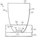
- FIGS. 1-4are diagrammatic representations of optical systems comprising a lens 105 separated by a gap from an LED 110 .
- the LEDcan be a lateral LED as shown in FIGS. 1 and 2 , a flip-chip LED as illustrated in FIG. 3 , a vertical LED as illustrated in FIG. 4 , or any other suitable type of LED or light source.
- LED 110can include a substrate 115 of any suitable LED substrate material including sapphire, silicon carbide, diamond, molded glass or other substrate material. Additionally, LED 110 can have non-substrate layers 120 that can include one or more layers or regions of doping, buffer layers or other layers.
- Non-substrate layers 120can include a light emitting region (or active region), typically a compound semiconductor such as InGaN or AlInGaP or AlGaN.
- LED 110can be rectangular (including square), hexagonal, circular or have another geometric or irregular shape.
- LED 110is mounted to a submount 125 .
- submount 125that can be made of a material with high thermal conductivity to spread and conduct the heat produced by LED 110 . Any suitable submount known or developed in the art can be used.
- LED 110is disposed in an LED cavity 130 defined by housing 135 .
- Housing 135can be a portion of a larger housing, a layer(s) of material mounted on submount 125 or other material positioned around LED 110 that forms a cavity in cooperation with submount 125 or other layer.
- material 135can be a layer of molded plastic mounted to submount 125 .
- LED cavity 130can have straight sidewalls that are parallel to the sides of the LED (i.e., vertical from the perspective of FIG. 1 ).
- the walls of LED cavity 130can be curved (e.g., parabolic, multi-parabolic or other curved shape), tapered or otherwise shaped to better direct light upwards.
- LED cavity 130can be filled with air, molded silicone, silicone mixed with phosphor particles, molded plastic, or other encapsulant.
- TIRtotal internal reflection
- a reflector 140(see FIG. 2 ) disposed around LED 110 can reflect light toward lens 105 .
- reflector 140can be a discrete component.
- the reflectorcan be Teflon, Teflon paper, diffuse reflective plastic, silver coated plastic, white paper, TiO2 coated material or other reflective material.
- reflector 140can be formed through selection of material 135 or the encapsulant.
- material 135can be a white plastic material such that the walls inherently form a diffuse white reflector.
- reflector 140can be formed by the surface tension of an encapsulant disposed in LED cavity 130 .
- an LEDmay only leak light out the sides of some portions of the LED.
- the substrate 115may include non-transparent sides such that LED 110 does not emit light from the sides of its substrate 115 . Consequently, optical system 110 can be constructed so reflector 140 only surrounds the side portions of LED 110 through which light is emitted.
- Lens 105can include an entrance face 150 to receive light into the lens body 107 of lens 105 .
- Lens body 105is the primary portion of lens 105 that is responsible for guiding or distributing light from an entrance face to an exit face. It should be noted, however, lens 105 can include additional layers, such as buffer or protective layers, that light may traverse prior to entering entrance face 150 .
- entrance face 150can be parallel to the primary emitting plane of LED 110 (e.g., a plane parallel to face 117 in FIG. 2 ).
- a phosphor layer 145can be disposed on lens 105 between the entrance face of lens body 107 and LED 110 .
- the phosphor layercan be disposed directly on the entrance face 150 or on a buffer layer between phosphor layer 145 and entrance face 150 .
- the phosphor in phosphor layer 145absorbs the higher energy, short wavelength light waves, and re-emits lower energy, longer wavelength light. Light emitted by phosphor layer 145 can enter the lens body 107 through entrance face 150 .
- phosphor layer 145can include a layer of phosphor particles in a binding material, such as silicone, coated on the entrance face 150 of lens body 107 .
- the phosphor particlescan include any suitably sized phosphor particles including, but not limited to, nano-phosphor particles, quantum dots, or smaller or larger particles and can include a single color or multiple colors of phosphor particles.
- the phosphor layer 145can be separated from the entrance face 150 of lens body 107 by one or more buffer layers. There may also be additional layers of material coupled to lens body 107 between phosphor layer 145 such that, for example, phosphor layer 145 is sandwiched between entrance face 150 layers material.
- one embodimentcan employ materials with matched or successively higher indexes of refraction as the layers get closer to lens body 107 without exceeding the index of refraction of lens body 107 .
- the color of light emitted by system 100can be selected based on LED 110 and the phosphor particles in phosphor layer 145 .
- LED 110can be a UV LED and phosphor layer 145 can include phosphors that down convert UV light to red, green, blue, yellow or other color light.
- LED 110can be a blue LED and phosphor layer 145 can down convert the blue light into a desired color.
- Reflector 140can be selected to reflect both the color light emitted by the LED 110 and the down converted light from phosphor layer 145 .
- Lens 105is positioned so that phosphor layer 145 is maintained a distance from LED 110 .
- the position of lens 105can be maintained by a housing, coupling lens 105 to encapsulant in LED cavity 130 or otherwise positioning lens 105 relative LED 110 . If lens 105 is adhered to an encapsulant, an adhesive with an index of refraction equal to or greater than that of the encapsulant can be used to prevent TIR at the encapsulant/adhesive boundary.
- Lens 105can act as a light guide to guide light from entrance face 150 to exit face 155 .
- Examples of a lens 105 that can utilize TIR at shaped sidewalls 157 to guide light to exit face 155are described below and in United Sates, Provisional Patent Application No. 60/756,845, entitled “Optical Device”, to Duong et al., filed Jan. 5, 2006 and U.S. patent application Ser. No. 11/649,018 entitled “Separate Optical Device for Directing Light from an LED,” filed Jan. 3, 2007, each of which is hereby fully incorporated by reference herein.
- Lens 105can be a separate optical device designed so that all the light can be extracted out exit face 155 (not accounting for Fresnel losses) in the smallest package design possible through selection of exit face area 155 , distance between the exit face 155 and entrance face 150 and the design of sidewalls 157 .
- Other embodimentscan be shaped to have different sizes or achieve different extraction efficiencies.
- lens 105can be configured such that at least 70% of the light entering lens body 107 at entrance 150 exits exit face 155 . Lenses 105 with lower extraction efficiencies can also be used. Additionally, the lens 105 can be selected to provide a uniform light distribution and to emit light at a desired half-angle.
- lens 105can be selected as described below in conjunction with FIGS. 19A-19D .
- Other embodiments of lensescan also be used, including, but not limited to, dome, Fresnel, conical, tapered or other lenses.
- the lens body 107can be a solid piece of material having a single index of refraction.
- LED 110produces light that can exit LED 110 from surface 117 (see FIG. 2 ) and sides 119 (see FIG. 2 ).
- Reflector 140acts as a redirecting lens to redirect light escaping sides 119 to entrance surface 150 of lens body 107 .
- phosphor layer 145down converts the light and emits light into lens body 107 and back into LED cavity 130 .
- Reflector 140can again direct the light in LED cavity 130 to entrance face 150 .
- Lens body 107guides light entering entrance face 150 from phosphor layer 145 to exit face 155 . If lens body 107 provides light in a uniform distribution in a desired half-angle, the need for additional lenses is not required to shape the beam. Consequently, color conversion and beam shaping can be achieved with a single lens.
- lens body 107can be constructed of a material that can withstand continuous use at this temperature.
- a buffer layer of silicon or other material capable of withstanding high temperaturescan be introduced between the phosphor layer 145 and entrance face 150 of lens 105 . While thicker or thinner buffers can be used, one embodiment can include a layer of silicon that is 100 to 200 microns thick. This can allow, for example, polycarbonates to be used for lens body 107 .
- FIGS. 5 and 6are diagrammatic representations of embodiments of lens 105 having body 107 , a buffer 160 layer and phosphor layer 145 .
- the buffer layercan be a suitable, high temperature material such as silicon or other material that can withstand the operating temperatures of the selected phosphor layer 145 .
- buffer 160can be adhered to or otherwise coupled to the bottom of lens body 107 or, as shown in FIG. 7 , all or a portion of buffer 160 can rest in a pocket formed at the entrance face of lens 105 .
- the phosphor layercan be disposed on lens 105 as a coating on buffer layer 160 .
- FIGS. 5 and 6also illustrate an adhesive layer 165 to adhere lens 105 to an encapsulant in LED cavity 130 ( FIGS. 1-4 ). To prevent TIR, each successive layer, including adhesives, can have a higher or the same index of refraction as the layer below it, with no layer between LED 110 and lens 105 having a higher index of refraction than lens body 107 .
- Embodiments described hereinprovide an advantage over traditional systems of using phosphors with LEDs because the phosphor is removed a distance from the LED. Because the phosphor is located at the entrance of the lens, there is high coupling efficiency. Additionally, self-heating of the phosphor due to Stoke's shift can be reduced because heat can be dissipated through the material of lens 140 , housing 135 and/or submount 125 . Higher phosphor conversion efficiency can also be achieved due to low flux density at the entrance face 150 of lens 105 .
- the distance between phosphor 145 and LED 110can be optimized to provide an optimal balance between thermal considerations and effective phosphor package efficiencies. While any suitable gap size can be used as needed or desired, one embodiment of an optical system has a gap of 100-200 microns between surface 117 (see FIG. 2 ) and phosphor layer 145 .
- embodiments described hereinprovide for flexible optical system architectures. Because the phosphor coated lens can be separate from the LED chip, it can be used in conjunction with various types of optical devices, including conventional light emitting devices. Furthermore, LEDs 110 can be used with a variety of different lens types depending on need.
- lenses 105can be tightly packed in an array.
- an array of lenses 105can be formed where each lens 105 is selected to emit light in a desired half-angle having a uniform distribution in near and far fields.
- the lenses 105can be spaced so that there are no perceivable gaps between emitted light for adjacent lenses 105 . Because the emitted light from each lens 105 is uniform and in a desired half-angle, the light output of the array will be in the desired half-angle with uniform near and far field distributions, but covering a larger area than the light emitted by a single lens. This provides a very practical benefit for display or lighting manufacturers because additional optics are no longer required to get light from an LED array using phosphors into a desired angle.
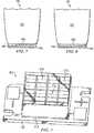
- FIG. 7is a diagrammatic representation of one embodiment of a packaged array 200 .
- packaged array 200comprises submount 125 , main housing 205 and cover 210 .
- Submount 125provides mechanical support and electrical connections for LEDs.
- Embodiments of submount materialsinclude, but are not limited to: Low Temperature Cofire Ceramic (LTCC) with thermal vias, High Temperature Cofire Ceramic (HTCC) with thermal vias, Beryllium Oxide (BeO) ceramic, Alumina ceramic, Silicon, Aluminum Nitride (AlN), Metal (Cu, Al, etc.), and Flex circuit.
- LTCCLow Temperature Cofire Ceramic
- HTCCHigh Temperature Cofire Ceramic
- BeOBeryllium Oxide
- Main housing 205can be formed of suitable materials including, but not limited to, plastic, thermoplastic, and other types of polymeric materials. Composite materials or other engineered materials may also be used. In some embodiments, main housing 205 may be made by a plastic injection molding manufacturing process. Various molding processes and other types of manufacturing processes may also be used. In some embodiments, main housing 205 may be opaque. In some embodiments, main housing 205 may be transparent or semi-transparent. Main housing 205 can be bonded or otherwise coupled to a layer of material 215 to complete the housing about the LEDs and lenses. In other embodiments, the housing can be formed of any number of layers or pieces of suitable material that will not unacceptably deform during operation due to heating and can protect the LEDs and lens for expected contact or shock during use, transportation or manufacture.
- packaged array 200is a 4 ⁇ 4 array and each group of 4 lenses shares a cover 210 .
- a single cover 210can be used for all lenses or each lens can have its own cover 210 .
- Cover 210can have a sufficient thickness to prevent the lenses from becoming damaged during handling of packaged array 200 .
- FIG. 8is a diagrammatic representation of a cross-sectional view of one embodiment of packaged array 200 illustrating main housing 205 , lens 105 , cover 210 , LED 110 , LED cavity 130 , housing layer 215 and submount 125 (only on instance of each is indicated for clarity).
- cover 210is integrated with lens 105 such that they form a single lens assembly.
- Cover 210can be integrated with other lenses 105 so that a single lens assembly will have a cover portion and multiple lens portions.
- the body 107 of lens 105 and cover 210can be made of a single piece of molded plastic, polycarbonate or other material. In other embodiments, cover 210 can be coupled to lens 105 using an adhesive.
- Cover 210also may simply be in contact with lens 105 or may be separated from lens 105 by a gap.
- cover 210 and any adhesive or other layers between lens 105 and cover 210can have indexes of refraction selected to prevent TIR at the exit face of lens 105 .
- the shape of lens body 107can be selected to account for the transition into cover 210 .
- Cover 210can be an optically transparent material, such as a plastic, glass, composite material, or other material and may include one or more layers. Additionally, cover 210 may include layers of material to perform photon conversion (e.g., an additional phosphor layer, filtering or other functions with respect to light exiting lens 105 .
- photon conversione.g., an additional phosphor layer, filtering or other functions with respect to light exiting lens 105 .
- Main housing 205forms a lens cavity 220 sized to fit lens 105 .
- the sidewalls 225 of lens cavity 220can be curved to match or approximate the sidewall shapes of lens 105 so that the size of lens cavity 220 is smaller proximate to the corresponding LED cavity 130 and larger distal from LED cavity 130 .
- the sidewalls 225can be vertically straight (from the perspective of FIG. 8 ) or can be tapered.
- Sidewalls 225can include reflective coatings or other coatings to reflect any light leaking from the sides of lens 105 to the exit of cover 205 .
- main housing 205can be formed of white plastic or other color material so that sidewalls 225 form reflectors.
- lens cavity 220can be sized so that there is a gap between the sidewalls of lens body 107 and sidewalls 225 of lens cavity 220 to preserve TIR in lens body 107 .
- the size of the gapcan be constant or can increase or decrease further from the base of lens cavity 220 .
- the gapcan be filled with air or other material.
- the materialhas a lower index of refraction than body 107 of lens 105 .
- sidewalls 225can contact sidewalls of lens body 107 and act as a reflector for light in lens body 107 .
- Main housing 205can include a shoulder 230 on which ledge 235 of cover 210 rests.
- An adhesive, mechanical fasteners or other suitable fastening mechanismcan be used to couple cover 210 to main housing 205 .
- a secondary structuresuch as a clamping structure, can maintain cover 210 against main housing 205 .
- lens 105is held in a desired position in lens cavity 220 .
- lens 105may not require additional attachment to cover 205 .
- a portion of lens 105can be adhered to or otherwise coupled to a shoulder 240 at the base of lens cavity 220 or other portion(s) of lens 105 can be coupled to main housing 205 .
- Main housing 205defines a portion or all of LED cavity 130 in cooperation with submount 125 and housing layer 215 .
- LED cavity 130is shown with vertical sidewalls, LED cavity 130 can have tapered, curved or otherwise shaped sidewalls to act as a redirector lens.
- the opening to LED cavity 130can have the same shape as and be rotationally aligned with LED 110 or can have another shape or alignment.
- a phosphor layercan be disposed proximate to entrance face 150 such that light exiting LED cavity 130 will be incident on the phosphor layer.
- the phosphor layerdown converts light before the light enters lens body 107 .
- the down converted lightis guided through lens 105 and exits cover 210 .
- Entrance face 150 of lens body 107can be the same shape as and be rotationally aligned with the opening to LED cavity 130 or have another shape or alignment.
- FIG. 9is a diagrammatic representation of a cutaway view of one embodiment of an LED cavity 130 .
- Submount 125forms the base of the cavity, while the sidewalls are formed by main housing 205 and layer 215 .
- a portion of LED 110can extend into the portion of LED cavity 130 defined by main housing 205 .
- the non-substrate layers 120 including the active region of the LEDmay extend into this opening or, in a flip chip design, the substrate 115 may extend into this portion.
- LED cavity 130can become larger closer to submount 125 to accommodate electrical connections or otherwise provide space around LED 110 . While portions of submount 125 , layer 215 and main housing 205 are shown, the packaged array 200 can include additional layers that define cavity 130 .
- FIG. 10is a diagrammatic representation of packaged array 200 with main housing 205 removed. It can be noted in FIG. 10 that the entrance face 150 to lens body 107 is maintained a distance away from the corresponding LED 110 . Consequently, any phosphors disposed on or near the entrance face will also be separated from LED 110 .
- FIG. 11is a diagrammatic representation of one embodiment of a portion of packaged array 200 showing layer 215 and submount 125 .
- Layer 215can be adhered or otherwise coupled to submount 125 .
- Layer 215can form a portion of LED cavity 130 around LED 110 . While, in the embodiment of FIG. 11 , LED cavity 130 has straight vertical sidewalls, LED cavity 130 can have curved, tapered or otherwise shaped sidewalls and can act as a reflector.
- the area of LED cavity 130 defined by layer 215can be larger than that defined by main housing 205 to accommodate electrical connections or to otherwise provide space around LED 110 . In other embodiments, the cavity can have a uniform size or become wider as it approaches lens 105 .
- Cavity 130can be entirely or partially filled with an encapsulant, air, silicone “goop”, or other filler material.
- FIG. 12is a diagrammatic representation of one embodiment of LEDs 110 mounted on submount 125 .
- Submount 125as illustrated in FIG. 12 , can provide support for LEDs 110 and provide electrical connections 250 . Electrical connections can be provided using suitable metals or other conductors. While a particular pattern and type of electrical connection are illustrated, any suitable electrical connections to LED 110 and submount 125 can be provided.
- FIG. 13is a diagrammatic representation of one embodiment of main housing 204 defining lens cavities 220 sized to fit lenses 105 .
- Lens cavity 220extends from an opening 260 to LED cavity 130 to a second opening 265 .
- the sizes of the openingscan have, according to one embodiment, a ratio that is the same as the size ratio of the exit face to entrance face of the lens.
- opening 260may be approximately the same size as the entrance face to the lens 105 while opening 265 is larger than the exit face.
- Sidewalls 225can be curved, tapered, vertical or have another selected shape.
- a shoulder 230provides a surface to which cover 210 can be coupled.
- main housing 205forms a 4 ⁇ 4 array.
- main housing 205can accommodate larger or smaller arrays or a single optical system.
- main housing 205can be shaped to accommodate circular, hexagonal or other shaped lenses 105 in a tightly packed array.
- FIGS. 8-13provide an example embodiment of a packaged LED. As discussed above, however, there may be additional portions of housing or other components in the packaged array.
- the embodiment of FIG. 14is similar to that of FIG. 8 , but also illustrates layer 255 .
- a portion of the cavity that houses LED 110can be formed by layer 255 rather than the main housing 205 .
- main housing 205can define lens cavities 220 with sidewalls that extend to layer 255 .
- Housing layers 255 and 215define the LED cavities 130 .
- Layers 215 and 255can include any suitable materials including plastics or other materials.
- Layer 255can be inset from layer 215 to form a ledge to which main housing 205 can be bonded.
- FIG. 15is a diagrammatic representation of one embodiment of a portion of a packaged array 200 with lenses 105 and cover 210 removed illustrating that layer 255 can define a portion of and provide an opening to LED cavity 130 .
- FIG. 16is a diagrammatic representation of a lens assembly 275 comprising portions with shape sidewalls that form lens bodies 107 of lenses 105 and a portion without shaped sidewalls that acts as cover 210 .
- the shaped and unshaped portionscan be a single piece of material.
- Each lens 105can be a phosphor coated lens selected to emit a desired color light. If more than one phosphor lens is used in a system, multiple types of phosphors may be used to achieve the desired color temperature and CRI. For instance, three yellow phosphor lenses and one red phosphor lens may be used in conjunction with a blue pump to attain warm white light.
- each of the four phosphor lenscan emit to the same far field distribution, the colors will undergo superposition and will not bleed or create ring-like effects.
- each lensin the 2 ⁇ 2 array of lenses shown, each lens can be selected to emit red, green or blue light. The light from lenses 105 can be combined to form white light.
- each assembly 275can emit a single color light. In a 4 ⁇ 4 array as shown in FIG. 7 , for example, four lens assemblies 275 can be used. One lens assembly 275 can emit blue light, one assembly 275 can emit red light and two assemblies 275 can emit green light such that the array as whole acts as a white light source.
- a lens assembly 275can include any number of lenses 105 .
- lenses 105can be configured with lens bodies 107 shaped to conserve radiance (or come within an acceptable percentage of conserving radiance), control the emission angle of light and emit light with a uniform or other desired distribution. As long as lenses 105 are tightly enough packed, there will be no gaps between the light emitted by lenses 105 . Consequently, the light emitted by array 200 as a whole will be within the desired half-angle and appear uniform with no dark spots or ghosting.
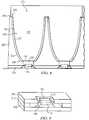
- FIG. 1illustrates an embodiment of a lens 105 having a lens body 107 with an entrance face 150 , an exit face 155 and sidewalls 157 .
- lens 105can be constructed with the assumption that phosphor layer 145 will emit uniformly into entrance face 150 .
- the area of exit face 155is selected according to the lumina equation such that:
- n 1 2 ⁇ A 1 ⁇ ⁇ 1 n 2 2 ⁇ ⁇ 2A 2 [ EQN . ⁇ 1 ]
- ⁇ 1effective solid angle whereby light enters through entrance face 150 ;
- ⁇ 2effective solid angle whereby light leaves exit face 155 ;
- a 1area of entrance face 150 ;
- a 2area of exit face 155 ;
- n 1refractive index of material of lens body 107 ;
- n 2refractive index of substance external to the exit face 155 of lens body 107 (e.g. air or other medium).
- a 1is the size of the phosphor layer and that the phosphor layer acts as a uniform emitter over that area.
- the size of the exit facecan be based on the area of the entrance face covered by phosphor, even if the physical size of the entrance face is larger.
- the area of exit face 155is within 30% (plus or minus) of the minimum area necessary to conserve radiance.
- the distance between exit face 155 and entrance face 150can be selected so that all rays having a straight transmission path from entrance face 150 to exit face 155 are incident on exit face 155 at less than or equal to the critical angle at exit face 155 to prevent TIR at exit face 155 .
- the minimum distancecan be selected based on a limiting ray.
- the limiting rayis a ray that travels the longest straight line distance from entrance face 150 to exit face 155 .
- the limiting raywill be a ray that travels from a corner of entrance face 150 to the opposite corner of exit face 155 .
- the distance between the entrance face 155 and exit face 155is within 30% of this minimum distance.
- the sidewalls 157can be shaped. Broadly speaking, the sidewall shapes are determined so that any ray incident on a sidewall is reflected to exit face 155 and is incident on exit face 155 at the critical angle or less (i.e., so that there is no loss due to internal reflection at exit face 155 ). While, in one embodiment, the sidewalls are shaped so that all rays that encounter the inner surface of the sidewalls experience total internal reflection to exit face 155 and are incident on exit face 155 at the critical angle or less, other sidewall shapes that allow some loss can be used.
- FIG. 17Ais a diagrammatic representation of a cross-section of a model of lens 305 for determining sidewall shapes.
- Sidewall shapescan be determined using computer-aided design.
- a model of the sidewallcan be created in a computer-aided design package and simulations run to determine an appropriate sidewall shape.
- each sidewallcan be divided into n facets with each facet being a planar section.
- model sidewall 370is made of fifteen planar facets 372 a - 372 o rather than a continuous curve.
- the variables of each facetcan be iteratively adjusted and the resulting distribution profiles analyzed until a satisfactory profile is achieved as described below. While the example of fifteen facets is used, each sidewall can be divided into any number of facets, including twenty or more facets.
- Each facetcan be analyzed with respect to reflecting a certain subset of rays within a lens.
- This area of interestcan be defined as an “angular subtense.”
- the angular subtense for a facetmay be defined in terms of the angles of rays emanating from a predefined point.
- the point selectedis one that will give rays with the highest angles of incidence on the facet because such rays are the least likely to experience TIR at the facet. In a lens with a square shaped entrance area, for example, this will be a point on the opposite edge of the entrance.
- the maximum of angle 374 of any ray that will be incident on a given sidewalle.g., sidewall 370
- ray 376 emanating from point 378establishes the maximum angle 374 for sidewall 370 .
- each facet(assuming an even distribution of angular subtenses) will correspond to a 3.2 degree band of angle 374 (e.g., a first facet will be the area on which rays emanating from point 378 with an angle 17 of 0-3.2 degrees are incident, the second facet will be the area on which rays emanating 374 from point 378 with an angle 95 of 3.2-6.4 degrees are incident, and so on).
- the exit angle, facet size, tilt angle, or other parameter of the facetcan be set so that all rays incident on the facet experience TIR and are reflected to exit surface 355 such that they are incident on exit surface 355 with an angle of incidence of less than or equal to the critical angle.
- the sidewallsare also shaped so that a ray viewed in a cross-sectional view only hits a side wall once. However, there may be additional reflection from a sidewall out of plane of the section. For a full 3D analysis, a ray that strikes a first sidewall near a corner, may then bounce over to a second side wall, adjacent to the first, and from there to the exit face.
- a curve fit or other numerical analysismay be performed to create a curved sidewall shape that best fits the desired facets.
- a simulated detector plane 380can be established.
- Detector plane 380can include x number of detectors to independently record incident power.
- a simulation of light passing through the lens 305may be performed and the intensity and irradiance distributions as received by detector plane 380 analyzed. If the intensity and irradiance distributions are not satisfactory for a particular application, the angles and angular subtenses of the facets can be adjusted, a new curved surface generated and the simulation re-performed until a satisfactory intensity profile, exitance profile or other light output profile is reached. Additional detector planes can be analyzed to ensure that both near field and far field patterns are satisfactory.
- the simulation(s)can be performed using the facets rather than curved surfaces and the surface curves determined after a desired light output profile is reached.
- the sidewallscan remain faceted and no curve be generated.
- the sidewall shapecan be selected based on multiple parabolas with each planer facet representing a linear approximation of a portion of a parabola.
- FIG. 17Bis a diagrammatic representation of a portion of a modeled lens 305 .
- a hypothetical ray 384is depicted that emanates from the focus 386 of a parabola 388 and intersects sidewall 370 such that it is reflected off sidewall 370 due to TIR and traverses the lens 305 to intersect exit plane 355 at an exit angle 390 that is less than the critical angle and exits lens 305 into air or other medium.
- FIG. 17Bis a diagrammatic representation of a portion of a modeled lens 305 .
- a hypothetical ray 384is depicted that emanates from the focus 386 of a parabola 388 and intersects sidewall 370 such that it is reflected off sidewall 370 due to TIR and traverses the lens 305 to intersect exit plane 355 at an exit angle 3
- ray 384bends as described by Snell's law. Since the tangent point of the sidewall is determined from a parabola and because the ray incident and reflected off the sidewall is in the same medium, the ray will be parallel to the optical axis of the parabola. Thus, light is projected with a half-angle 392 .
- Angular subtenses 396 defining the shape of sidewall 370may be adjusted so that hypothetical ray 384 reflects off sidewall 370 such that ray 384 traverses exit face 355 with a desired exit angle 390 or projects light with a desired half angle 392 .
- finer subtensesmay be used towards the base of the sidewall (i.e. nearer the phosphor layer) because the effects of the subtense are greater or more acute upon reflection near the base, and thus finer subtenses allow for a sidewall with better TIR properties, whereas further from the base, where the effects of the subtenses are less, the subtenses may be coarser.
- facets of a sidewallmay be numerically greater towards the base of a lens body 107 .
- a sidewallmay have 20 or more facets, with finer facets at the base of the sidewall, wherein the facets approximate one or more subtenses.
- a facetcan be a linear approximation of a portion of a parabola 388 .
- the parameters of parabola 388can be adjusted until the portion achieves the desired goal of all rays incident on the portion reflecting to exit face 355 such that the rays have an exit angle 390 of less than the critical angle.
- Each facetcan be formed from a parabola having different parameters.
- a facet for one angular subtensemay be based on a parabola while another facet is based on another parabola.
- a 20-facet sidewallfor example, may be based on 20 different parabolas.
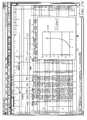
- FIG. 17Cdepicts a spreadsheet 500 that can be utilized to design a sidewall shape as shown in graph 510 through the specification of angular subtenses.
- Projected half angle column 550contains a plurality of angles that correspond to projected half angle 450 of FIG. 4B .
- Exit angle columns 540 a (in radians) and 540 b (in degrees)contain a plurality of exit angles corresponding to exit angle 392 of FIG. 17B . More particularly, all or a subset of the angles in column 540 a may be angles that are less than the critical angle such that light rays intersecting the exit face at those angles traverse the exit face, exiting the shaped device.
- Angular subtense column 565contains a plurality of angles (in radians) that define the limits of an angular subtense that can be used in conjunction with parabola focus column 560 to define the shape of a sidewall such that a ray reflects off the sidewall to exit the exit face at less than the critical angle.
- theta column 570 and radius column 575can be developed wherein corresponding values in columns 570 and 575 correspond to points on a desired parabola for the angular subtense.
- theta column 570 and radius column 575can be utilized to develop Cartesian coordinates for points on a sidewall (e.g. coordinate transformation columns 577 ) that approximate the parabola for the angular subtense.
- a usercan specify the size of the entrance face of the shaped device (in this case marked LED size) and material index.
- the sizecan correspond to the size of the entrance face or emitting size of the phosphor layer.
- a row in screen 500can be completed as follows.
- the usercan specify an exit angle in air (assuming air is the medium in which the lens will operate) in column 550 .
- the userhas selected 55.3792 degrees.
- the exit angle in the lenscan be calculated as sin(55.3792/180* ⁇ ) ⁇ tilde over ( ) ⁇ /.1.77 or 0.4649323 radians, column 540 a .
- the radius of the parabola (column 575 ) for the first facetcan be calculated as 2*.732466/(1+cos(124.5883/180* ⁇ )).
- the X, Y coordinatescan then be used as data point inputs for a shape fitting chart in Excel.
- graph 510is based on the data points in the X and Y columns (with the Y column values used as x-axis coordinates and the X column values used as y-axis coordinates in graph 510 ).
- a starting valuecan be set (e.g., 0.5 and 0).
- the shape from graph 510can be entered into an optical design package and simulations run. If a simulation is unsatisfactory, the user can adjust the values in spreadsheet 500 until a satisfactory profile is achieved.
- FIG. 17Dprovides a diagrammatic representation of one embodiment of lens body 107 with sidewalls shaped to cause TIR so that rays are reflected from the sidewalls to the exit surface.
- the shape of each sidewallin this embodiment, is a superposition of multiple contoured surfaces as defined by the various facets. While a curve fit is performed for ease of manufacturability, other embodiments can retain faceted sidewalls.
- the exit plane of light for purposes of shaping a lensis the exit face of the lens.
- the exit plane of the shaped lens 105may be the transition from shaped portion into another portion such as cover 210 . If cover 210 is the same material as or has the same index of refraction as the shaped portion, the exit plane can be the transition between the shaped portion of lens body 107 and cover 210 .
- FIG. 18illustrates a lens 105 having a shaped lens body 107 and cover 210 as an integrated lens 105 .
- the transition 400 between shaped lens body 107 and cover 210can serve as the “exit face” for determining the shape of lens 105 as described above. If cover 210 has the same index of refraction as lens body 107 , then the critical angle at the used in shaping lens 105 will be the same as if transition 400 were exposed to the outside medium because if light traverses transition 400 at less than or equal to the critical angle, it will also be incident on surface 404 at less than or equal to the critical angle. If the index of refraction of cover 210 is lower (or any adhesives or other layers between cover 210 and lens body 107 ) is lower, the critical angle at the exit face will be the critical angle based on the lower index of refraction.
- the minimum area of exit surface 155can be determined from EQN. 1 above, which relies on various effective solid angles.
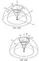
- the effective solid angle of lightis determined based on equations derived from sources that radiate as Lambertian emitters, but that are treated as points because the distances of interest are much greater than the size of the source.
- the observed Radiant Intensity (flux/steradian) of a Lambertian sourcevaries with the angle to the normal of the source by the cosine of that angle.
- a sphere 630 of given radius (R)surrounds point source 632 (in this example, point source 632 approximates a Lambertian source at a significant distance).
- the projected area of a hemisphere of the sphereis ⁇ R 2 and the projected area of the full sphere is 2 ⁇ R 2 .
- This modelcan be used to design lens because the phosphors can be modeled as a Lambertian emitter such that from any point on a hypothetical hemisphere centered over the interface, a given point on the interface will have the same radiance.
- the area A 3can be calculated as the flat, circular surface (e.g., surface 636 ) that is subtended by the beam solid angle of interest using a radius of the circle 634 (R c ) that is the distance from the normal ray to the intersection of the spherical surface.
- the area A 3is the projected area of the solid angle as it intersects the sphere.
- ⁇is 90 degrees, leading to a projected solid angle of ⁇ *Sin 2 (90), and for the desired half angle of 30 degrees, the projected solid angle is ⁇ *Sin 2 (30).
- a 2can be determined for any half angle.
- the solid angleis determined using equations derived from a Lambertian source modeled as a point source. These equations do not consider the fact that light may enter a lens body 107 through an interface that may be square, rectangular, circular, oval or otherwise shaped. While the above-described method can give a good estimate of the solid angle, which can be later adjusted if necessary based on empirical or computer simulation testing, other methods of determining the effective solid angle can be used.
- FIGS. 20A-20Edescribe another method for determining the effective solid angle for a lens.
- FIG. 20Ais a diagrammatic representation of one embodiment of an entrance face 750 and an exit face 755 of a lens 760 and a hypothetical target plane 756 onto which light is projected.
- FIG. 20Aillustrates examples for a position of an effective source origin 752 , central normal 753 and effective output origin 754 .
- the center of interface 750is at 0,0,0 in a Cartesian coordinate system.
- Target plane 756represents the parameters of the resulting pattern (e.g., size and half angle used by other optics).
- the half angle at the diagonalis the starting point.
- ⁇ 1 for a square- or rectangular-faced separate optical deviceis 30 degrees.
- ⁇ 119.47 degrees.
- a similar calculationcan be performed for a ray projecting from a point on the long and short sides of entrance surface 150 .
- ⁇ 2 and ⁇ 2can be determined for a ray traveling from the center of one edge on entrance surface 450 to the center of the opposite edge of exit surface 755 .
- the critical angleis the same at 19.47, but ⁇ 1 is not the same as ⁇ 2 .
- ⁇ 2is determined by the geometry of the sides and the height to the optical device.
- Z epsis the distance the effective point source is displaced from the emitting surface of the LED.
- X F1cos( ⁇ 1 )sin( ⁇ 1 ) [EQN. 7]
- Y F1cos( ⁇ 1 )sin( ⁇ 1 ) [EQN. 8]
- Z F1cos( ⁇ 1 [EQN. 9]
- X F2cos( ⁇ 2 ) [EQN. 10]
- Y F2sin( ⁇ 2 ) [EQN. 11]
- Z F2cos( ⁇ 2 ) [EQN.
- a similar methodology based on the geometries previously calculatedcan be used to determine other points (e.g., for example, the location of points T 1 and T 2 can be determined based on the location of points F 1 and F 2 and the desired half angle of light at target plane 756 .)
- FIG. 20Dillustrates the diagonal rays and one ray from the short side projected onto a sphere 759 for exit face 755 and sphere 761 for target plane 756 .
- the projection of the intersection of the edge rays at the sphere 759 onto the plane of the exit face 755forms elliptical segments.
- the projection of the diffracted exit rays at the edge of the target faceintersect the sphere 761 .
- FIG. 20Epoints out the circular intersection 763 of the rays lying in the plane formed by the edge 764 of target face 756 intersecting sphere 761 (illustrated at 762), and the projection 762 of that intersection onto the target plane 756 .
- the effective solid anglecan be determined for the target plane using EQN. 3B.
- the effective solid angle for the optical devicecan be determined. For example, the total projected area is determined as described above and inserted as “projected area of desired solid angle” in equation 3B.
- the minimum surface area to conserve brightnesscan be determined empirically.
- the minimum surface area calculations aboveassume 100% of the emitting entrance face of the separate optical device is receiving light, the phosphor layer may be disposed over only a part of the entrance surface such that a smaller entrance surface area is used.
- the calculations of the minimum area of the exit planecan be adjusted to account of the actual area receiving light. That is, the actual area of the phosphor layer can used as A 1 .
- the lens body 107can be optimized for use with a phosphor layer 145 as a uniform emitter at the entrance face using modeling as described above.
- Lenses according to embodiments described hereincan project light into a desired cone angle of 10-60 degrees with a theoretical efficiency of up to 96% in the lens body (meaning that 96% of the light received from the phosphors is emitted in the desired half-angles with 4% Fresnel loss).
- the efficiencycan be 100% without Fresnel losses.
- lens bodiescan be used to provide greater efficiency than other technologies, while also producing uniform or near uniform intensity distributions at both near and far fields.
- lens body 107can use TIR to cause reflection
- lens body 107may have reflective coating or the sidewalls of a lens cavity can act as the reflector.
- critical anglesare is the same for the sidewalls of the lens body as the exit face, they can be different.
- a lens body 107can be surrounded by a medium other than air in a lens cavity 107 while the exit face 155 or cover 210 is exposed to air.
- each lensis used in conjunction with a single LED
- a lenscan also be used with an array of LEDs emitting light on the phosphor layer.
- FIG. 21is a diagrammatic representation of one embodiment of a system in which a solid dome lens 280 is used.
- LED 110is disposed in an LED cavity 130 having tapered sidewalls that act as a reflector 140 .
- a layer of phosphor 145covers the entrance face of the body 282 of dome lens 280 .
- FIG. 22is a diagrammatic representation of another embodiment of an optical system.
- encapsulant in the LED cavity 130 around LED 110forms a convex portion 285 .
- a lens 105 having a phosphor coating 145can be adhered to convex portion 275 or to a housing or another structure.
- the optical systemcan be assembled such that there is no air gap between lens 105 and convex portion 285 .
- lens 105can include a concave entrance face.
- an intermediate layer with a concave entrance facecan be used.
- FIG. 23is a diagrammatic representation of another embodiment.
- lens 805includes a pocket 810 at the entrance face 815 to lens body 807 .
- Phosphor particles 820can be packed in the pocket and held in place with a binding material or with another layer 825 of material.
- Material 825is preferably an optically transparent material that can withstand the temperatures of phosphor 820 .
- FIG. 24illustrates yet another embodiment of a lens 830 in which a layer of phosphor 835 is sandwiched between a buffer layer 840 and another layer of suitable material 845 .
- the stack of layerscan be coupled to a lens body 850 .
- the layers of materialcan include glass, polycarbonate, silicon or other layers.
Landscapes
- Physics & Mathematics (AREA)
- General Physics & Mathematics (AREA)
- Optics & Photonics (AREA)
- Led Device Packages (AREA)
Abstract
Description
RC=R*Sin(θ) [EQN. 2]
The area equals:
A3=πRC2=π(R*Sin(θ))2 [EQN. 3A]
Ω=π{projected area of desired solid angle}/(projected area of hemisphere) [EQN. 3B]
n2Sin(α1)=n1Sin(β1) [EQN. 5]
where n1is the IOR of the
- n2is the IOR of the material (typically air) into which the light is projected from the
lens 760; - α1is the half angle at the exit face in the medium external to the
lens 760; - β1is the desired half angle of
lens 760.
- n2is the IOR of the material (typically air) into which the light is projected from the
XF1=cos(ψ1)sin(β1) [EQN. 7]
YF1=cos(ψ1)sin(β1) [EQN. 8]
ZF1=cos(β1 [EQN. 9]
XF2=cos(ψ2) [EQN. 10]
YF2=sin(β2) [EQN. 11]
ZF2=cos(β2) [EQN. 12]
where ψ1is the angle of the diagonal ray in the X-Y plane (45 degrees for a square) and where ψ2=90 degrees for a ray projecting from the middle of a side parallel to the X axis as shown in
Claims (16)
Priority Applications (9)
| Application Number | Priority Date | Filing Date | Title |
|---|---|---|---|
| US12/646,570US8449128B2 (en) | 2009-08-20 | 2009-12-23 | System and method for a lens and phosphor layer |
| TW099127809ATW201126114A (en) | 2009-08-20 | 2010-08-19 | System and method for a phosphor coated lens |
| KR1020127006808AKR20120090975A (en) | 2009-08-20 | 2010-08-20 | System and method for a phosphor coated lens |
| PCT/US2010/046108WO2011022610A1 (en) | 2009-08-20 | 2010-08-20 | System and method for a phosphor coated lens |
| CN2010800428809ACN102686936A (en) | 2009-08-20 | 2010-08-20 | System and method for a phosphor coated lens |
| EP10810640AEP2467638A1 (en) | 2009-08-20 | 2010-08-20 | System and method for a phosphor coated lens |
| JP2012525714AJP2013502695A (en) | 2009-08-20 | 2010-08-20 | System and method for phosphor-coated lenses |
| US13/077,594US8585253B2 (en) | 2009-08-20 | 2011-03-31 | System and method for color mixing lens array |
| US14/057,768US9086211B2 (en) | 2009-08-20 | 2013-10-18 | System and method for color mixing lens array |
Applications Claiming Priority (2)
| Application Number | Priority Date | Filing Date | Title |
|---|---|---|---|
| US23549109P | 2009-08-20 | 2009-08-20 | |
| US12/646,570US8449128B2 (en) | 2009-08-20 | 2009-12-23 | System and method for a lens and phosphor layer |
Related Child Applications (1)
| Application Number | Title | Priority Date | Filing Date |
|---|---|---|---|
| US13/077,594Continuation-In-PartUS8585253B2 (en) | 2009-08-20 | 2011-03-31 | System and method for color mixing lens array |
Publications (2)
| Publication Number | Publication Date |
|---|---|
| US20110044022A1 US20110044022A1 (en) | 2011-02-24 |
| US8449128B2true US8449128B2 (en) | 2013-05-28 |
Family
ID=43605237
Family Applications (1)
| Application Number | Title | Priority Date | Filing Date |
|---|---|---|---|
| US12/646,570Expired - Fee RelatedUS8449128B2 (en) | 2009-08-20 | 2009-12-23 | System and method for a lens and phosphor layer |
Country Status (1)
| Country | Link |
|---|---|
| US (1) | US8449128B2 (en) |
Cited By (42)
| Publication number | Priority date | Publication date | Assignee | Title |
|---|---|---|---|---|
| US20130094181A1 (en)* | 2010-06-22 | 2013-04-18 | Matthias Bruemmer | Phosphor Device and Lighting Apparatus Comprising the Same |
| US8585253B2 (en) | 2009-08-20 | 2013-11-19 | Illumitex, Inc. | System and method for color mixing lens array |
| US20140166902A1 (en)* | 2011-08-01 | 2014-06-19 | Dirk Berben | Wavelength Conversion Body And Method For Manufacturing Same |
| US20140225147A1 (en)* | 2011-09-13 | 2014-08-14 | Osram Opto Semiconductors Gmbh | Method for Producing a Plurality of Opto-Electronic Components and Opto-Electronic Component |
| US8896003B2 (en) | 2006-01-05 | 2014-11-25 | Illumitex, Inc. | Separate optical device for directing light from an LED |
| US20140355302A1 (en)* | 2013-03-15 | 2014-12-04 | Cree, Inc. | Outdoor and/or Enclosed Structure LED Luminaire for General Illumination Applications, Such as Parking Lots and Structures |
| US9291320B2 (en) | 2013-01-30 | 2016-03-22 | Cree, Inc. | Consolidated troffer |
| US9366396B2 (en) | 2013-01-30 | 2016-06-14 | Cree, Inc. | Optical waveguide and lamp including same |
| US9366799B2 (en) | 2013-03-15 | 2016-06-14 | Cree, Inc. | Optical waveguide bodies and luminaires utilizing same |
| US9389367B2 (en) | 2013-01-30 | 2016-07-12 | Cree, Inc. | Optical waveguide and luminaire incorporating same |
| US9411086B2 (en) | 2013-01-30 | 2016-08-09 | Cree, Inc. | Optical waveguide assembly and light engine including same |
| US9442243B2 (en) | 2013-01-30 | 2016-09-13 | Cree, Inc. | Waveguide bodies including redirection features and methods of producing same |
| USD770552S1 (en)* | 2014-05-30 | 2016-11-01 | Osram Sylvania Inc. | Flexible optic |
| US9513424B2 (en) | 2013-03-15 | 2016-12-06 | Cree, Inc. | Optical components for luminaire |
| US9581750B2 (en) | 2013-03-15 | 2017-02-28 | Cree, Inc. | Outdoor and/or enclosed structure LED luminaire |
| US9625638B2 (en) | 2013-03-15 | 2017-04-18 | Cree, Inc. | Optical waveguide body |
| US9632295B2 (en) | 2014-05-30 | 2017-04-25 | Cree, Inc. | Flood optic |
| US9690029B2 (en) | 2013-01-30 | 2017-06-27 | Cree, Inc. | Optical waveguides and luminaires incorporating same |
| US9719660B1 (en) | 2016-01-28 | 2017-08-01 | Ecosense Lighting Inc. | Compositions for LED light conversions |
| US20170261186A1 (en)* | 2016-03-08 | 2017-09-14 | Lilibrand Llc | Lighting system with lens assembly |
| US9772073B2 (en) | 2016-01-28 | 2017-09-26 | Ecosense Lighting Inc. | Illuminating with a multizone mixing cup |
| US9798072B2 (en) | 2013-03-15 | 2017-10-24 | Cree, Inc. | Optical element and method of forming an optical element |
| US9869432B2 (en) | 2013-01-30 | 2018-01-16 | Cree, Inc. | Luminaires using waveguide bodies and optical elements |
| US9887319B2 (en)* | 2012-02-09 | 2018-02-06 | Oculus Vr, Llc | Enhanced light extraction |
| US9920901B2 (en) | 2013-03-15 | 2018-03-20 | Cree, Inc. | LED lensing arrangement |
| US10197226B2 (en) | 2016-01-28 | 2019-02-05 | Ecosense Lighting Inc | Illuminating with a multizone mixing cup |
| US10209429B2 (en) | 2013-03-15 | 2019-02-19 | Cree, Inc. | Luminaire with selectable luminous intensity pattern |
| US20190265548A1 (en)* | 2017-03-03 | 2019-08-29 | Apple Inc. | Displays with Direct-lit Backlight Units |
| US10416377B2 (en) | 2016-05-06 | 2019-09-17 | Cree, Inc. | Luminaire with controllable light emission |
| US10422944B2 (en) | 2013-01-30 | 2019-09-24 | Ideal Industries Lighting Llc | Multi-stage optical waveguide for a luminaire |
| US10436970B2 (en) | 2013-03-15 | 2019-10-08 | Ideal Industries Lighting Llc | Shaped optical waveguide bodies |
| US20190309922A1 (en)* | 2016-07-28 | 2019-10-10 | HELLA GmbH & Co. KGaA | Light source with a primary lens made of silicone and a method for manufacturing the light source |
| US10502899B2 (en)* | 2013-03-15 | 2019-12-10 | Ideal Industries Lighting Llc | Outdoor and/or enclosed structure LED luminaire |
| US11028980B2 (en) | 2013-10-30 | 2021-06-08 | Ecosense Lighting Inc. | Flexible strip lighting apparatus and methods |
| US11041609B2 (en) | 2018-05-01 | 2021-06-22 | Ecosense Lighting Inc. | Lighting systems and devices with central silicone module |
| US11047534B2 (en) | 2016-01-28 | 2021-06-29 | EcoSense Lighting, Inc. | Multizone mixing cup illumination system |
| US11112083B2 (en) | 2013-03-15 | 2021-09-07 | Ideal Industries Lighting Llc | Optic member for an LED light fixture |
| US11296057B2 (en) | 2017-01-27 | 2022-04-05 | EcoSense Lighting, Inc. | Lighting systems with high color rendering index and uniform planar illumination |
| US11339932B2 (en) | 2017-03-09 | 2022-05-24 | Korrus, Inc. | Fixtures and lighting accessories for lighting devices |
| US11353200B2 (en) | 2018-12-17 | 2022-06-07 | Korrus, Inc. | Strip lighting system for direct input of high voltage driving power |
| US11719882B2 (en) | 2016-05-06 | 2023-08-08 | Ideal Industries Lighting Llc | Waveguide-based light sources with dynamic beam shaping |
| US12388056B1 (en) | 2017-01-27 | 2025-08-12 | Korrus, Inc. | Linear lighting systems and processes |
Families Citing this family (66)
| Publication number | Priority date | Publication date | Assignee | Title |
|---|---|---|---|---|
| US9412926B2 (en) | 2005-06-10 | 2016-08-09 | Cree, Inc. | High power solid-state lamp |
| CN102022637A (en)* | 2009-09-09 | 2011-04-20 | 富士迈半导体精密工业(上海)有限公司 | Illuminating device |
| US9275979B2 (en) | 2010-03-03 | 2016-03-01 | Cree, Inc. | Enhanced color rendering index emitter through phosphor separation |
| US10359151B2 (en) | 2010-03-03 | 2019-07-23 | Ideal Industries Lighting Llc | Solid state lamp with thermal spreading elements and light directing optics |
| US9316361B2 (en) | 2010-03-03 | 2016-04-19 | Cree, Inc. | LED lamp with remote phosphor and diffuser configuration |
| US9310030B2 (en) | 2010-03-03 | 2016-04-12 | Cree, Inc. | Non-uniform diffuser to scatter light into uniform emission pattern |
| US9500325B2 (en) | 2010-03-03 | 2016-11-22 | Cree, Inc. | LED lamp incorporating remote phosphor with heat dissipation features |
| US9625105B2 (en) | 2010-03-03 | 2017-04-18 | Cree, Inc. | LED lamp with active cooling element |
| US8632196B2 (en) | 2010-03-03 | 2014-01-21 | Cree, Inc. | LED lamp incorporating remote phosphor and diffuser with heat dissipation features |
| US8562161B2 (en) | 2010-03-03 | 2013-10-22 | Cree, Inc. | LED based pedestal-type lighting structure |
| WO2011145247A1 (en)* | 2010-05-18 | 2011-11-24 | シャープ株式会社 | Display device |
| US10451251B2 (en)* | 2010-08-02 | 2019-10-22 | Ideal Industries Lighting, LLC | Solid state lamp with light directing optics and diffuser |
| US9234655B2 (en) | 2011-02-07 | 2016-01-12 | Cree, Inc. | Lamp with remote LED light source and heat dissipating elements |
| US11251164B2 (en) | 2011-02-16 | 2022-02-15 | Creeled, Inc. | Multi-layer conversion material for down conversion in solid state lighting |
| US20120250320A1 (en)* | 2011-03-31 | 2012-10-04 | Xicato, Inc. | Color conversion cavities for led-based illumination modules |
| US9046241B2 (en) | 2011-11-12 | 2015-06-02 | Jingqun Xi | High efficiency directional light source using lens optics |
| US9488359B2 (en) | 2012-03-26 | 2016-11-08 | Cree, Inc. | Passive phase change radiators for LED lamps and fixtures |
| WO2013152234A1 (en)* | 2012-04-04 | 2013-10-10 | Axlen, Inc. | Optically efficient solid-state lighting device packaging |
| US20150233536A1 (en)* | 2012-04-17 | 2015-08-20 | Soraa, Inc. | Phosphor-coated element in a lamp cavity |
| JP5980577B2 (en)* | 2012-05-31 | 2016-08-31 | シチズン電子株式会社 | Side-illuminated LED light-emitting device and method for manufacturing side-illuminated LED light-emitting device |
| US20130329429A1 (en)* | 2012-06-11 | 2013-12-12 | Cree, Inc. | Emitter package with integrated mixing chamber |
| US20140146543A1 (en)* | 2012-11-26 | 2014-05-29 | Magic Lighting Optics | Outdoor lighting device |
| US9952372B2 (en) | 2013-03-15 | 2018-04-24 | Cree, Inc. | Luminaire utilizing waveguide |
| US11408572B2 (en) | 2014-03-15 | 2022-08-09 | Ideal Industries Lighting Llc | Luminaires utilizing optical waveguide |
| US10317608B2 (en) | 2014-03-15 | 2019-06-11 | Cree, Inc. | Luminaires utilizing optical waveguide |
| US9835317B2 (en) | 2014-03-15 | 2017-12-05 | Cree, Inc. | Luminaire utilizing waveguide |
| US9709725B2 (en) | 2013-03-15 | 2017-07-18 | Cree, Inc. | Luminaire utilizing waveguide |
| WO2014145283A1 (en)* | 2013-03-15 | 2014-09-18 | Cree, Inc. | Optical waveguide body |
| US9568662B2 (en) | 2013-03-15 | 2017-02-14 | Cree, Inc. | Optical waveguide body |
| KR102081246B1 (en)* | 2013-04-15 | 2020-02-25 | 엘지전자 주식회사 | Display apparatus |
| US9368939B2 (en) | 2013-10-18 | 2016-06-14 | Soraa Laser Diode, Inc. | Manufacturable laser diode formed on C-plane gallium and nitrogen material |
| US9520695B2 (en) | 2013-10-18 | 2016-12-13 | Soraa Laser Diode, Inc. | Gallium and nitrogen containing laser device having confinement region |
| US9379525B2 (en) | 2014-02-10 | 2016-06-28 | Soraa Laser Diode, Inc. | Manufacturable laser diode |
| US9362715B2 (en) | 2014-02-10 | 2016-06-07 | Soraa Laser Diode, Inc | Method for manufacturing gallium and nitrogen bearing laser devices with improved usage of substrate material |
| US9798070B2 (en) | 2013-11-05 | 2017-10-24 | Philips Lighting Holding B.V. | Light emitting device |
| US9651740B2 (en) | 2014-01-09 | 2017-05-16 | Cree, Inc. | Extraction film for optical waveguide and method of producing same |
| US9209596B1 (en) | 2014-02-07 | 2015-12-08 | Soraa Laser Diode, Inc. | Manufacturing a laser diode device from a plurality of gallium and nitrogen containing substrates |
| US9871350B2 (en) | 2014-02-10 | 2018-01-16 | Soraa Laser Diode, Inc. | Manufacturable RGB laser diode source |
| US9520697B2 (en) | 2014-02-10 | 2016-12-13 | Soraa Laser Diode, Inc. | Manufacturable multi-emitter laser diode |
| US9360188B2 (en) | 2014-02-20 | 2016-06-07 | Cree, Inc. | Remote phosphor element filled with transparent material and method for forming multisection optical elements |
| RU2671285C2 (en)* | 2014-05-13 | 2018-10-30 | Коэлюкс С.Р.Л. | Source of light and lighting system, imitating sunlight |
| US10935211B2 (en) | 2014-05-30 | 2021-03-02 | Ideal Industries Lighting Llc | LED luminaire with a smooth outer dome and a cavity with a ridged inner surface |
| US12372219B2 (en)* | 2014-05-30 | 2025-07-29 | Cree Lighting Usa Llc | LED luminaire with a cavity, finned interior, and a curved outer wall extending from a surface on which the light source is mounted |
| US9246311B1 (en) | 2014-11-06 | 2016-01-26 | Soraa Laser Diode, Inc. | Method of manufacture for an ultraviolet laser diode |
| US12126143B2 (en) | 2014-11-06 | 2024-10-22 | Kyocera Sld Laser, Inc. | Method of manufacture for an ultraviolet emitting optoelectronic device |
| US9653642B1 (en) | 2014-12-23 | 2017-05-16 | Soraa Laser Diode, Inc. | Manufacturable RGB display based on thin film gallium and nitrogen containing light emitting diodes |
| US9666677B1 (en) | 2014-12-23 | 2017-05-30 | Soraa Laser Diode, Inc. | Manufacturable thin film gallium and nitrogen containing devices |
| US11437775B2 (en) | 2015-08-19 | 2022-09-06 | Kyocera Sld Laser, Inc. | Integrated light source using a laser diode |
| US10879673B2 (en) | 2015-08-19 | 2020-12-29 | Soraa Laser Diode, Inc. | Integrated white light source using a laser diode and a phosphor in a surface mount device package |
| US10938182B2 (en) | 2015-08-19 | 2021-03-02 | Soraa Laser Diode, Inc. | Specialized integrated light source using a laser diode |
| US11437774B2 (en) | 2015-08-19 | 2022-09-06 | Kyocera Sld Laser, Inc. | High-luminous flux laser-based white light source |
| US12385623B2 (en) | 2016-01-28 | 2025-08-12 | Korrus, Inc. | Beam-shaping lighting systems |
| US10501025B2 (en) | 2016-03-04 | 2019-12-10 | Ford Global Technologies, Llc | Vehicle badge |
| DE102017117027B3 (en)* | 2017-07-27 | 2018-12-13 | SMR Patents S.à.r.l. | Projection device, review device and motor vehicle |
| KR102631105B1 (en)* | 2017-08-31 | 2024-01-30 | 니치아 카가쿠 고교 가부시키가이샤 | Light emitting device |
| US11239637B2 (en) | 2018-12-21 | 2022-02-01 | Kyocera Sld Laser, Inc. | Fiber delivered laser induced white light system |
| US11421843B2 (en) | 2018-12-21 | 2022-08-23 | Kyocera Sld Laser, Inc. | Fiber-delivered laser-induced dynamic light system |
| US12000552B2 (en) | 2019-01-18 | 2024-06-04 | Kyocera Sld Laser, Inc. | Laser-based fiber-coupled white light system for a vehicle |
| US12152742B2 (en) | 2019-01-18 | 2024-11-26 | Kyocera Sld Laser, Inc. | Laser-based light guide-coupled wide-spectrum light system |
| US11884202B2 (en) | 2019-01-18 | 2024-01-30 | Kyocera Sld Laser, Inc. | Laser-based fiber-coupled white light system |
| US10903623B2 (en) | 2019-05-14 | 2021-01-26 | Soraa Laser Diode, Inc. | Method and structure for manufacturable large area gallium and nitrogen containing substrate |
| US11228158B2 (en) | 2019-05-14 | 2022-01-18 | Kyocera Sld Laser, Inc. | Manufacturable laser diodes on a large area gallium and nitrogen containing substrate |
| EP3951259B1 (en)* | 2019-05-23 | 2024-04-03 | Suzhou Opple Lighting Co., Ltd. | Illumination lamp |
| US20230161127A1 (en)* | 2020-04-15 | 2023-05-25 | CommScope Connectivity Belgium BV | Device and method for sealing cables in telecommunications enclosures |
| US12191626B1 (en) | 2020-07-31 | 2025-01-07 | Kyocera Sld Laser, Inc. | Vertically emitting laser devices and chip-scale-package laser devices and laser-based, white light emitting devices |
| JP2023028365A (en)* | 2021-08-19 | 2023-03-03 | 株式会社ジャパンディスプレイ | optical device |
Citations (496)
| Publication number | Priority date | Publication date | Assignee | Title |
|---|---|---|---|---|
| US1670837A (en) | 1924-01-31 | 1928-05-22 | Gen Motors Corp | Head-lamp reflector |
| US3981023A (en) | 1974-09-16 | 1976-09-14 | Northern Electric Company Limited | Integral lens light emitting diode |
| US3988633A (en) | 1975-01-30 | 1976-10-26 | Duro-Test Corporation | Fluorescent lamp with envelope grooves |
| US4125890A (en) | 1976-12-10 | 1978-11-14 | Corning Glass Works | Parabolic reflector including filament locating means |
| US4180755A (en) | 1976-12-10 | 1979-12-25 | Corning Glass Works | Sealed beam lamp including filament locating means |
| US4239369A (en) | 1978-11-20 | 1980-12-16 | Gte Products Corporation | Camera and reflector having offset optical and mechanical axes |
| US4304479A (en) | 1980-07-28 | 1981-12-08 | Polaroid Corporation | Photographic lighting apparatus |
| US4388633A (en) | 1980-09-29 | 1983-06-14 | Hughes Aircraft Company | Monolithic transistor coupled electroluminescent diode |
| US4439910A (en) | 1980-09-29 | 1984-04-03 | Hughes Aircraft Company | Process for fabrication of monolithic transistor coupled electroluminescent diode |
| US4486364A (en) | 1981-12-04 | 1984-12-04 | Stanley Electric Company, Ltd. | Method and apparatus for molding a synthetic resin lens for a light emitting diode |
| US4501637A (en) | 1981-06-12 | 1985-02-26 | Motorola, Inc. | LED having self-aligned lens |
| US4716507A (en) | 1986-05-12 | 1987-12-29 | The United States Of America As Represented By The Secretary Of The Army | Optical collimator target illumination |
| US4728999A (en) | 1980-06-25 | 1988-03-01 | Pitney Bowes Inc. | Light emitting diode assembly |
| US4740259A (en) | 1985-09-13 | 1988-04-26 | Siemens Aktiengesellschaft | Method of making a light-emitting-diode (led) with spherical lens |
| US4799136A (en) | 1987-05-29 | 1989-01-17 | Guth Lighting Systems, Inc. | Lighting fixture having concave shaped reflector and improved asymmetric light reflection system |
| US4966862A (en) | 1989-08-28 | 1990-10-30 | Cree Research, Inc. | Method of production of light emitting diodes |
| US5036339A (en) | 1989-09-05 | 1991-07-30 | Eastman Kodak Company | LED array into floating focusing structure for differential expansion |
| US5087949A (en) | 1989-06-27 | 1992-02-11 | Hewlett-Packard Company | Light-emitting diode with diagonal faces |
| US5114513A (en) | 1988-10-27 | 1992-05-19 | Omron Tateisi Electronics Co. | Optical device and manufacturing method thereof |
| US5126929A (en) | 1991-01-09 | 1992-06-30 | R & D Molded Products, Inc. | LED holder with lens |
| US5151718A (en) | 1990-12-31 | 1992-09-29 | Texas Instruments Incorporated | System and method for solid state illumination for dmd devices |
| US5174649A (en) | 1991-07-17 | 1992-12-29 | Precision Solar Controls Inc. | Led lamp including refractive lens element |
| EP0534843A1 (en) | 1991-09-25 | 1993-03-31 | Raclet | Framework for rectangular tent with a double inclined roof |
| US5218216A (en) | 1987-01-31 | 1993-06-08 | Toyoda Gosei Co., Ltd. | Gallium nitride group semiconductor and light emitting diode comprising it and the process of producing the same |
| US5233204A (en) | 1992-01-10 | 1993-08-03 | Hewlett-Packard Company | Light-emitting diode with a thick transparent layer |
| US5251117A (en) | 1991-02-21 | 1993-10-05 | Nec Corporation | Structure of a diffusing lens for a light emitting diode |
| US5272108A (en) | 1991-02-27 | 1993-12-21 | Kabushiki Kaisha Toyota Chuo Kenkyusho | Method of manufacturing gallium nitride semiconductor light-emitting device |
| US5278433A (en) | 1990-02-28 | 1994-01-11 | Toyoda Gosei Co., Ltd. | Light-emitting semiconductor device using gallium nitride group compound with double layer structures for the n-layer and/or the i-layer |
| US5281830A (en) | 1990-10-27 | 1994-01-25 | Toyoda Gosei Co., Ltd. | Light-emitting semiconductor device using gallium nitride group compound |
| US5315490A (en) | 1989-10-13 | 1994-05-24 | Bastable Rodney C | Light fittings |
| US5369289A (en) | 1991-10-30 | 1994-11-29 | Toyoda Gosei Co. Ltd. | Gallium nitride-based compound semiconductor light-emitting device and method for making the same |
| US5523591A (en) | 1995-01-25 | 1996-06-04 | Eastman Kodak Company | Assembly of led array and lens with engineered light output profile and method for making the assembly |
| US5528720A (en) | 1992-03-23 | 1996-06-18 | Minnesota Mining And Manufacturing Co. | Tapered multilayer luminaire devices |
| US5563422A (en) | 1993-04-28 | 1996-10-08 | Nichia Chemical Industries, Ltd. | Gallium nitride-based III-V group compound semiconductor device and method of producing the same |
| US5578156A (en) | 1994-01-07 | 1996-11-26 | Sumitomo Electric Industries, Ltd. | Method of mounting a lens on a light emitting diode |
| US5587593A (en) | 1994-04-20 | 1996-12-24 | Toyoda Gosei Co., Ltd. | Light-emitting semiconductor device using group III nitrogen compound |
| US5620557A (en) | 1993-12-27 | 1997-04-15 | Toyoda Gosei Co., Ltd. | Sapphireless group III nitride semiconductor and method for making same |
| US5652438A (en) | 1994-07-20 | 1997-07-29 | Toyoda Gosei Co., Ltd. | Light-emitting semiconductor device using group III nitride compound |
| US5654831A (en) | 1995-01-04 | 1997-08-05 | Hughes Electronics | Refractive ellipsoid optical surface without spherical aberration |
| US5667297A (en) | 1994-08-29 | 1997-09-16 | U.S. Philips Corporation | Electric reflector lamp |
| US5700713A (en) | 1994-03-22 | 1997-12-23 | Toyoda Gosei Co., Ltd. | Light emitting semiconductor device using group III nitride compound and method of producing the same |
| US5739554A (en) | 1995-05-08 | 1998-04-14 | Cree Research, Inc. | Double heterojunction light emitting diode with gallium nitride active layer |
| US5780867A (en) | 1996-03-07 | 1998-07-14 | Sandia Corporation | Broadband light-emitting diode |
| US5790583A (en) | 1995-05-25 | 1998-08-04 | Northwestern University | Photonic-well Microcavity light emitting devices |
| US5813753A (en) | 1997-05-27 | 1998-09-29 | Philips Electronics North America Corporation | UV/blue led-phosphor device with efficient conversion of UV/blues light to visible light |
| US5839424A (en) | 1996-04-16 | 1998-11-24 | Hct Shaping System Sa | Process for the orientation of several single crystals disposed side by side on a cutting support for their simultaneous cutting in a cutting machine and device for practicing this process |
| US5846844A (en) | 1993-11-29 | 1998-12-08 | Toyoda Gosei Co., Ltd. | Method for producing group III nitride compound semiconductor substrates using ZnO release layers |
| US5862167A (en) | 1994-07-19 | 1999-01-19 | Toyoda Gosei Co., Ltd. | Light-emitting semiconductor device using gallium nitride compound |
| US5912477A (en) | 1994-10-07 | 1999-06-15 | Cree Research, Inc. | High efficiency light emitting diodes |
| US5945689A (en) | 1995-03-17 | 1999-08-31 | Toyoda Gosei Co., Ltd. | Light-emitting semiconductor device using group III nitride compound |
| US5953469A (en) | 1996-10-29 | 1999-09-14 | Xeotron Corporation | Optical device utilizing optical waveguides and mechanical light-switches |
| US5959401A (en) | 1996-05-21 | 1999-09-28 | Toyoda Gosei Co., Ltd. | Light-emitting semiconductor device using group III nitride compound |
| US5998925A (en) | 1996-07-29 | 1999-12-07 | Nichia Kagaku Kogyo Kabushiki Kaisha | Light emitting device having a nitride compound semiconductor and a phosphor containing a garnet fluorescent material |
| US6005722A (en) | 1998-09-04 | 1999-12-21 | Hewlett-Packard Company | Optical display system including a light valve |
| US6008539A (en) | 1995-06-16 | 1999-12-28 | Toyoda Gosei Co., Ltd. | Electrodes for p-type group III nitride compound semiconductors |
| US6023076A (en) | 1996-08-22 | 2000-02-08 | Toyoda Gosei Co., Ltd. | Group III nitride compound semiconductor light emitting device having a current path between electrodes |
| US6066861A (en) | 1996-09-20 | 2000-05-23 | Siemens Aktiengesellschaft | Wavelength-converting casting composition and its use |
| US6078064A (en) | 1998-05-04 | 2000-06-20 | Epistar Co. | Indium gallium nitride light emitting diode |
| JP2000180962A (en) | 1998-12-18 | 2000-06-30 | Sony Corp | Projection illuminating device |
| US6093941A (en) | 1993-09-09 | 2000-07-25 | The United States Of America As Represented By The Secretary Of The Navy | Photonic silicon on a transparent substrate |
| US6118908A (en) | 1994-09-09 | 2000-09-12 | Gemfire Corporation | Integrated optical device with phosphor in substrate pit |
| US6133589A (en) | 1999-06-08 | 2000-10-17 | Lumileds Lighting, U.S., Llc | AlGaInN-based LED having thick epitaxial layer for improved light extraction |
| US6144536A (en) | 1997-02-13 | 2000-11-07 | Honeywell International Inc. | Illumination system with light recycling to enhance brightness |
| US6169294B1 (en) | 1998-09-08 | 2001-01-02 | Epistar Co. | Inverted light emitting diode |
| US6177761B1 (en) | 1996-07-17 | 2001-01-23 | Teledyne Lighting And Display Products, Inc. | LED with light extractor |
| US6185051B1 (en) | 1999-06-23 | 2001-02-06 | Read-Rite Corporation | High numerical aperture optical focusing device for use in data storage systems |
| US6194742B1 (en) | 1998-06-05 | 2001-02-27 | Lumileds Lighting, U.S., Llc | Strain engineered and impurity controlled III-V nitride semiconductor films and optoelectronic devices |
| US6201262B1 (en) | 1997-10-07 | 2001-03-13 | Cree, Inc. | Group III nitride photonic devices on silicon carbide substrates with conductive buffer interlay structure |
| US6222207B1 (en) | 1999-05-24 | 2001-04-24 | Lumileds Lighting, U.S. Llc | Diffusion barrier for increased mirror reflectivity in reflective solderable contacts on high power LED chip |
| US6221683B1 (en) | 1997-05-27 | 2001-04-24 | Osram Opto Semiconductor Gmbh & Co. Ohg | Method for producing a light-emitting component |
| US6229160B1 (en) | 1997-06-03 | 2001-05-08 | Lumileds Lighting, U.S., Llc | Light extraction from a semiconductor light-emitting device via chip shaping |
| US6229782B1 (en) | 1998-07-06 | 2001-05-08 | Read-Rite Corporation | High numerical aperture optical focusing device for use in data storage systems |
| US6257737B1 (en) | 1999-05-20 | 2001-07-10 | Philips Electronics Na | Low-profile luminaire having a reflector for mixing light from a multi-color linear array of LEDs |
| US6258618B1 (en) | 1998-09-11 | 2001-07-10 | Lumileds Lighting, Us, Llc | Light emitting device having a finely-patterned reflective contact |
| US6271622B1 (en) | 1997-04-28 | 2001-08-07 | Osram Sylvania Inc. | Vehicle lamps with improved filament and filament support configurations |
| US6274924B1 (en) | 1998-11-05 | 2001-08-14 | Lumileds Lighting, U.S. Llc | Surface mountable LED package |
| US6287947B1 (en) | 1999-06-08 | 2001-09-11 | Lumileds Lighting, U.S. Llc | Method of forming transparent contacts to a p-type GaN layer |
| US6307218B1 (en) | 1998-11-20 | 2001-10-23 | Lumileds Lighting, U.S., Llc | Electrode structures for light emitting devices |
| US6310364B1 (en) | 1998-08-03 | 2001-10-30 | Toyoda Gosei Co., Ltd. | Light-emitting apparatus |
| US6331450B1 (en) | 1998-12-22 | 2001-12-18 | Toyoda Gosei Co., Ltd. | Method of manufacturing semiconductor device using group III nitride compound |
| US6335999B1 (en) | 1992-03-23 | 2002-01-01 | Minnesota Mining & Mfg. Co. | Multilayer luminaire device |
| US6337493B1 (en) | 1999-04-21 | 2002-01-08 | Nichia Corporation | Nitride semiconductor device |
| US20020012247A1 (en) | 2000-07-28 | 2002-01-31 | Toyoda Gosei Co., Ltd. | Lighting device |
| US20020017844A1 (en) | 2000-03-06 | 2002-02-14 | Parkyn William A. | LED light source with field-of-view-controlling optics |
| USD453745S1 (en) | 1999-12-27 | 2002-02-19 | Nichia Corporation | Light emitting diode |
| US6351069B1 (en) | 1999-02-18 | 2002-02-26 | Lumileds Lighting, U.S., Llc | Red-deficiency-compensating phosphor LED |
| US6350041B1 (en) | 1999-12-03 | 2002-02-26 | Cree Lighting Company | High output radial dispersing lamp using a solid state light source |
| US6356700B1 (en) | 1998-06-08 | 2002-03-12 | Karlheinz Strobl | Efficient light engine systems, components and methods of manufacture |
| US20020030194A1 (en) | 2000-09-12 | 2002-03-14 | Camras Michael D. | Light emitting diodes with improved light extraction efficiency |
| US6361192B1 (en) | 1999-10-25 | 2002-03-26 | Global Research & Development Corp | Lens system for enhancing LED light output |
| US6364487B1 (en) | 1999-01-29 | 2002-04-02 | Agilent Technologies, Inc. | Solid state based illumination source for a projection display |
| US6377535B1 (en) | 1998-07-06 | 2002-04-23 | Read-Rite Corporation | High numerical aperture optical focusing device having a conical incident facet and a parabolic reflector for use in data storage systems |
| US6410942B1 (en) | 1999-12-03 | 2002-06-25 | Cree Lighting Company | Enhanced light extraction through the use of micro-LED arrays |
| US20020080622A1 (en) | 2000-12-21 | 2002-06-27 | Philips Electronics North America Corporation | Faceted multi-chip package to provide a beam of uniform white light from multiple monochrome LEDs |
| US20020080615A1 (en) | 2000-12-22 | 2002-06-27 | Thomas Marshall | LED collimation optics with improved performance and reduced size |
| US6417019B1 (en) | 2001-04-04 | 2002-07-09 | Lumileds Lighting, U.S., Llc | Phosphor converted light emitting diode |
| US6443594B1 (en) | 2000-03-31 | 2002-09-03 | Koninklijke Philips Electronics N.V. | One-piece lens arrays for collimating and focusing light and led light generators using same |
| US6445011B1 (en) | 1999-01-29 | 2002-09-03 | Toyoda Gosei Co., Ltd. | Light-emitting diode |
| US20020123164A1 (en) | 2001-02-01 | 2002-09-05 | Slater David B. | Light emitting diodes including modifications for light extraction and manufacturing methods therefor |
| US20020127864A1 (en) | 1999-11-02 | 2002-09-12 | Smith John Stephen | Methods for creating elements of predetermined shape and apparatus using these elements |
| US6452214B2 (en) | 1999-03-31 | 2002-09-17 | Toyoda Gosei Co., Ltd. | Group III nitride compound semiconductor light-emitting device having a light emission output of high light intensity |
| US6459100B1 (en) | 1998-09-16 | 2002-10-01 | Cree, Inc. | Vertical geometry ingan LED |
| US20020141006A1 (en) | 2001-03-30 | 2002-10-03 | Pocius Douglas W. | Forming an optical element on the surface of a light emitting device for improved light extraction |
| US20020163808A1 (en) | 2001-05-04 | 2002-11-07 | West Robert S. | Lens and Lens Cap with Sawtooth Portion for Light Emitting Diode |
| US6478453B2 (en) | 2000-01-07 | 2002-11-12 | Koninklijke Philips Electronics N.V. | Luminaire |
| US6486499B1 (en) | 1999-12-22 | 2002-11-26 | Lumileds Lighting U.S., Llc | III-nitride light-emitting device with increased light generating capability |
| US6489636B1 (en) | 2001-03-29 | 2002-12-03 | Lumileds Lighting U.S., Llc | Indium gallium nitride smoothing structures for III-nitride devices |
| US6501102B2 (en) | 1999-09-27 | 2002-12-31 | Lumileds Lighting, U.S., Llc | Light emitting diode (LED) device that produces white light by performing phosphor conversion on all of the primary radiation emitted by the light emitting structure of the LED device |
| US20030002272A1 (en) | 2001-06-28 | 2003-01-02 | Yoshinobu Suehiro | Light-emitting diode |
| US6504171B1 (en) | 2000-01-24 | 2003-01-07 | Lumileds Lighting, U.S., Llc | Chirped multi-well active region LED |
| US6504179B1 (en) | 2000-05-29 | 2003-01-07 | Patent-Treuhand-Gesellschaft Fur Elektrische Gluhlampen Mbh | Led-based white-emitting illumination unit |
| US6502956B1 (en) | 1999-03-25 | 2003-01-07 | Leotek Electronics Corporation | Light emitting diode lamp with individual LED lenses |
| US6514782B1 (en) | 1999-12-22 | 2003-02-04 | Lumileds Lighting, U.S., Llc | Method of making a III-nitride light-emitting device with increased light generating capability |
| US6515313B1 (en) | 1999-12-02 | 2003-02-04 | Cree Lighting Company | High efficiency light emitters with reduced polarization-induced charges |
| US20030036217A1 (en) | 2001-08-16 | 2003-02-20 | Motorola, Inc. | Microcavity semiconductor laser coupled to a waveguide |
| US6526201B1 (en) | 2000-10-12 | 2003-02-25 | Delphi Technologies, Inc. | Light transport coupler assembly |
| US6526082B1 (en) | 2000-06-02 | 2003-02-25 | Lumileds Lighting U.S., Llc | P-contact for GaN-based semiconductors utilizing a reverse-biased tunnel junction |
| US6527411B1 (en) | 2000-08-01 | 2003-03-04 | Visteon Corporation | Collimating lamp |
| US6534797B1 (en) | 2000-11-03 | 2003-03-18 | Cree, Inc. | Group III nitride light emitting devices with gallium-free layers |
| US6541800B2 (en) | 2001-02-22 | 2003-04-01 | Weldon Technologies, Inc. | High power LED |
| US6563142B2 (en) | 2001-07-11 | 2003-05-13 | Lumileds Lighting, U.S., Llc | Reducing the variation of far-field radiation patterns of flipchip light emitting diodes |
| US20030089914A1 (en) | 2001-11-14 | 2003-05-15 | Solidlite Corporation | Surface-mounted devices of light-emitting diodes with small lens |
| US6573537B1 (en) | 1999-12-22 | 2003-06-03 | Lumileds Lighting, U.S., Llc | Highly reflective ohmic contacts to III-nitride flip-chip LEDs |
| US6576932B2 (en) | 2001-03-01 | 2003-06-10 | Lumileds Lighting, U.S., Llc | Increasing the brightness of III-nitride light emitting devices |
| US6576488B2 (en) | 2001-06-11 | 2003-06-10 | Lumileds Lighting U.S., Llc | Using electrophoresis to produce a conformally coated phosphor-converted light emitting semiconductor |
| US20030132447A1 (en) | 2002-01-11 | 2003-07-17 | Hitachi Cable Limited | Light-emitting diode array |
| USD477580S1 (en) | 2002-01-30 | 2003-07-22 | Nichia Corporation | Light emitting diode |
| US6598998B2 (en) | 2001-05-04 | 2003-07-29 | Lumileds Lighting, U.S., Llc | Side emitting light emitting device |
| US6603258B1 (en) | 2000-04-24 | 2003-08-05 | Lumileds Lighting, U.S. Llc | Light emitting diode device that emits white light |
| US6608330B1 (en) | 1998-09-21 | 2003-08-19 | Nichia Corporation | Light emitting device |
| US20030156416A1 (en) | 2002-02-21 | 2003-08-21 | Whelen Engineering Company, Inc. | Led light assembly |
| USD478877S1 (en) | 2001-11-21 | 2003-08-26 | Nichia Corporation | Light emitting diode |
| US6620643B1 (en) | 1999-08-05 | 2003-09-16 | Toyoda Gosei Co., Ltd. | Light-emitting device using group III nitride compound semiconductor |
| US6623142B1 (en) | 2002-02-15 | 2003-09-23 | Delphi Technologies, Inc. | Method and apparatus for correcting optical non-uniformities in a light emitting diode |
| US6630692B2 (en) | 2001-05-29 | 2003-10-07 | Lumileds Lighting U.S., Llc | III-Nitride light emitting devices with low driving voltage |
| US6630689B2 (en) | 2001-05-09 | 2003-10-07 | Lumileds Lighting, U.S. Llc | Semiconductor LED flip-chip with high reflectivity dielectric coating on the mesa |
| US6630691B1 (en) | 1999-09-27 | 2003-10-07 | Lumileds Lighting U.S., Llc | Light emitting diode device comprising a luminescent substrate that performs phosphor conversion |
| US6635503B2 (en) | 2002-01-28 | 2003-10-21 | Cree, Inc. | Cluster packaging of light emitting diodes |
| US6635904B2 (en) | 2001-03-29 | 2003-10-21 | Lumileds Lighting U.S., Llc | Indium gallium nitride smoothing structures for III-nitride devices |
| US6639733B2 (en) | 2000-03-16 | 2003-10-28 | Light Prescriptions Innovators, Llc. | High efficiency non-imaging optics |
| US6637921B2 (en) | 2001-09-28 | 2003-10-28 | Osram Sylvania Inc. | Replaceable LED bulb with interchangeable lens optic |
| US6642618B2 (en) | 2000-12-21 | 2003-11-04 | Lumileds Lighting U.S., Llc | Light-emitting device and production thereof |
| US6642652B2 (en) | 2001-06-11 | 2003-11-04 | Lumileds Lighting U.S., Llc | Phosphor-converted light emitting device |
| US6649943B2 (en) | 2001-06-07 | 2003-11-18 | Toyoda Gosei Co., Ltd. | Group III nitride compound semiconductor light-emitting element |
| US6649946B2 (en) | 1999-11-30 | 2003-11-18 | Osram Opto Semiconductors Gmbh | Light source using a yellow-to-red-emitting phosphor |
| USD482337S1 (en) | 2001-12-28 | 2003-11-18 | Nichia Corporation | Light emitting diode (LED) |
| US6650044B1 (en) | 2000-10-13 | 2003-11-18 | Lumileds Lighting U.S., Llc | Stenciling phosphor layers on light emitting diodes |
| USD482666S1 (en) | 2001-11-30 | 2003-11-25 | Nichia Corporation | Light emitting diode (LED) |
| US6657236B1 (en) | 1999-12-03 | 2003-12-02 | Cree Lighting Company | Enhanced light extraction in LEDs through the use of internal and external optical elements |
| US6657300B2 (en) | 1998-06-05 | 2003-12-02 | Lumileds Lighting U.S., Llc | Formation of ohmic contacts in III-nitride light emitting devices |
| US6664560B2 (en) | 2001-06-15 | 2003-12-16 | Cree, Inc. | Ultraviolet light emitting diode |
| EP1380469A2 (en) | 2002-07-11 | 2004-01-14 | Hella KG Hueck & Co. | Lighting device for vehicles |
| US6679621B2 (en) | 2002-06-24 | 2004-01-20 | Lumileds Lighting U.S., Llc | Side emitting LED and lens |
| US6680490B2 (en) | 2001-06-15 | 2004-01-20 | Toyoda Gosei Co., Ltd. | Light-emitting device |
| US6680569B2 (en) | 1999-02-18 | 2004-01-20 | Lumileds Lighting U.S. Llc | Red-deficiency compensating phosphor light emitting device |
| US6683327B2 (en) | 2001-11-13 | 2004-01-27 | Lumileds Lighting U.S., Llc | Nucleation layer for improved light extraction from light emitting devices |
| US6682331B1 (en) | 2002-09-20 | 2004-01-27 | Agilent Technologies, Inc. | Molding apparatus for molding light emitting diode lamps |
| US6682207B2 (en) | 1999-01-29 | 2004-01-27 | Lumileds Lighting U.S., Llc | Green phosphor converted light emitting diode |
| US20040016718A1 (en) | 2002-03-20 | 2004-01-29 | Ruey-Jen Hwu | Micro-optic elements and method for making the same |
| US6686691B1 (en) | 1999-09-27 | 2004-02-03 | Lumileds Lighting, U.S., Llc | Tri-color, white light LED lamps |
| US6696703B2 (en) | 1999-09-27 | 2004-02-24 | Lumileds Lighting U.S., Llc | Thin film phosphor-converted light emitting diode device |
| US20040036080A1 (en) | 2000-04-19 | 2004-02-26 | Georg Bogner | High radiance led chip and a method for producing same |
| US20040046489A1 (en) | 2002-09-09 | 2004-03-11 | Vetorino Steve Robert | LED light collection and uniform transmission system |
| US6711200B1 (en) | 1999-09-07 | 2004-03-23 | California Institute Of Technology | Tuneable photonic crystal lasers and a method of fabricating the same |
| US6717355B2 (en) | 2000-08-28 | 2004-04-06 | Toyoda Gosei Co., Ltd. | Light-emitting unit |
| US6717353B1 (en) | 2002-10-14 | 2004-04-06 | Lumileds Lighting U.S., Llc | Phosphor converted light emitting device |
| US20040079957A1 (en) | 2002-09-04 | 2004-04-29 | Andrews Peter Scott | Power surface mount light emitting die package |
| US6730939B2 (en) | 2000-02-15 | 2004-05-04 | Osram Opto Semiconductors Gmbh | Radiation emitting semiconductor device |
| US6730940B1 (en) | 2002-10-29 | 2004-05-04 | Lumileds Lighting U.S., Llc | Enhanced brightness light emitting device spot emitter |
| US6734467B2 (en) | 1999-11-03 | 2004-05-11 | Osram Opto Semiconductors Gmbh & Co. Ohg | LED white light source with broadband excitation |
| USD489690S1 (en) | 2003-06-05 | 2004-05-11 | Nichia Corporation | Light emitting diode (LED) |
| US6738175B2 (en) | 1999-12-13 | 2004-05-18 | Nichia Corporation | Light emitting device |
| US6737681B2 (en) | 2001-08-22 | 2004-05-18 | Nichia Corporation | Light emitting device with fluorescent member excited by semiconductor light emitting element |
| USD490387S1 (en) | 2001-11-22 | 2004-05-25 | Nichia Corporation | Light emitting diode |
| US6740906B2 (en) | 2001-07-23 | 2004-05-25 | Cree, Inc. | Light emitting diodes including modifications for submount bonding |
| US6744077B2 (en) | 2002-09-27 | 2004-06-01 | Lumileds Lighting U.S., Llc | Selective filtering of wavelength-converted semiconductor light emitting devices |
| USD490782S1 (en) | 1999-12-27 | 2004-06-01 | Nichia Corporation | Light emitting diode |
| US6744071B2 (en) | 2002-01-28 | 2004-06-01 | Nichia Corporation | Nitride semiconductor element with a supporting substrate |
| USD490784S1 (en) | 2002-05-01 | 2004-06-01 | Nichia Corporation | Light emitting diode |
| US6746124B2 (en) | 2001-02-06 | 2004-06-08 | Robert E. Fischer | Flashlight producing uniform high brightness |
| US6747298B2 (en) | 2001-07-23 | 2004-06-08 | Cree, Inc. | Collets for bonding of light emitting diodes having shaped substrates |
| US6746295B2 (en) | 1999-04-22 | 2004-06-08 | Osram-Opto Semiconductors Gmbh & Co. Ohg | Method of producing an LED light source with lens |
| USD491538S1 (en) | 2001-11-02 | 2004-06-15 | Nichia Corporation | Light emitting diode |
| US20040114393A1 (en) | 2001-12-10 | 2004-06-17 | Galli Robert D. | LED lighting assembly |
| USD491899S1 (en) | 2002-05-22 | 2004-06-22 | Nichia Corporation | Light emitting diode |
| US20040120153A1 (en) | 2002-12-20 | 2004-06-24 | Pate Michael A. | Non-imaging photon concentrator |
| US20040126913A1 (en) | 2002-12-06 | 2004-07-01 | Loh Ban P. | Composite leadframe LED package and method of making the same |
| US6764932B2 (en) | 1999-10-14 | 2004-07-20 | Cree, Inc. | Single step pendeo- and lateral epitaxial overgrowth of group III-nitride epitaxial layers with group III-nitride buffer layer and resulting structures |
| US6768525B2 (en) | 2000-12-01 | 2004-07-27 | Lumileds Lighting U.S. Llc | Color isolated backlight for an LCD |
| US6768136B2 (en) | 2001-08-14 | 2004-07-27 | Osram Opto Semiconductors Gmbh | Radiation emitting structural element |
| US6774405B2 (en) | 2001-03-05 | 2004-08-10 | Toyoda Gosei Co., Ltd. | Light-emitting device |
| US20040155565A1 (en) | 2003-02-06 | 2004-08-12 | Holder Ronald G. | Method and apparatus for the efficient collection and distribution of light for illumination |
| US6777871B2 (en) | 2000-03-31 | 2004-08-17 | General Electric Company | Organic electroluminescent devices with enhanced light extraction |
| US6784027B2 (en) | 2001-11-30 | 2004-08-31 | Osram Opto Semiconductors Gmbh | Light-emitting semiconductor component |
| USD495822S1 (en) | 2003-05-16 | 2004-09-07 | Ccs, Inc. | Attachment lens for LED |
| US6791116B2 (en) | 2002-04-30 | 2004-09-14 | Toyoda Gosei Co., Ltd. | Light emitting diode |
| US6791103B2 (en) | 1992-11-20 | 2004-09-14 | Nichia Corporation | Light-emitting gallium nitride-based compound semiconductor device |
| USD496007S1 (en) | 2001-11-21 | 2004-09-14 | Nichia Corporation | Light emitting diode |
| US6794690B2 (en) | 2001-09-18 | 2004-09-21 | Toyoda Gosei Co., Ltd. | Group III nitride compound semiconductor light-emitting element |
| US6794211B2 (en) | 1998-12-02 | 2004-09-21 | Samsung Electro-Mechanics Co., Ltd. | Light emitting diode and method of fabricating thereof |
| US6794684B2 (en) | 2001-02-01 | 2004-09-21 | Cree, Inc. | Reflective ohmic contacts for silicon carbide including a layer consisting essentially of nickel, methods of fabricating same, and light emitting devices including the same |
| US6800500B2 (en) | 1999-02-05 | 2004-10-05 | Lumileds Lighting U.S., Llc | III-nitride light emitting devices fabricated by substrate removal |
| US6800876B2 (en) | 2001-01-16 | 2004-10-05 | Cree, Inc. | Group III nitride LED with undoped cladding layer (5000.137) |
| US20040201987A1 (en) | 2003-04-09 | 2004-10-14 | Citizen Electronics Co., Ltd. | LED lamp |
| US6806571B2 (en) | 2000-03-27 | 2004-10-19 | Toyoda Gosei Co., Ltd. | III nitride compound semiconductor element an electrode forming method |
| US20040207774A1 (en) | 2003-04-17 | 2004-10-21 | Gothard David L. | Illumination apparatus for LCD/organic displays |
| US6812500B2 (en) | 1996-06-26 | 2004-11-02 | Osram Opto Semiconductors Gmbh & Co. Ohg. | Light-radiating semiconductor component with a luminescence conversion element |
| US20040218390A1 (en) | 2003-01-24 | 2004-11-04 | Digital Optics International Corporation | High-density illumination system |
| US6814470B2 (en) | 2000-05-08 | 2004-11-09 | Farlight Llc | Highly efficient LED lamp |
| US20040222426A1 (en) | 2003-05-07 | 2004-11-11 | Bear Hsiung | Light emitting diode module structure |
| US6819505B1 (en) | 2003-09-08 | 2004-11-16 | William James Cassarly | Internally reflective ellipsoidal collector with projection lens |
| US6819506B1 (en) | 2003-09-30 | 2004-11-16 | Infinity Trading Co. Ltd. | Optical lens system for projecting light in a lambertion pattern from a high power led light source |
| US20040233665A1 (en) | 2003-05-21 | 2004-11-25 | West Robert S. | Devices for creating brightness profiles |
| US6825501B2 (en) | 1997-08-29 | 2004-11-30 | Cree, Inc. | Robust Group III light emitting diode for high reliability in standard packaging applications |
| US6828599B2 (en) | 2000-10-05 | 2004-12-07 | Epivalley Co., Ltd. | Semiconductor light-emitting diode |
| USD499384S1 (en) | 2001-12-28 | 2004-12-07 | Nichia Corporation | Light emitting diode |
| US6828596B2 (en) | 2002-06-13 | 2004-12-07 | Lumileds Lighting U.S., Llc | Contacting scheme for large and small area semiconductor light emitting flip chip devices |
| US6831302B2 (en) | 2003-04-15 | 2004-12-14 | Luminus Devices, Inc. | Light emitting devices with improved extraction efficiency |
| US6831305B2 (en) | 2001-04-23 | 2004-12-14 | Toyoda Gosei Co., Ltd. | Semiconductor light-emitting device |
| US6833564B2 (en) | 2001-11-02 | 2004-12-21 | Lumileds Lighting U.S., Llc | Indium gallium nitride separate confinement heterostructure light emitting devices |
| US6835957B2 (en) | 2002-07-30 | 2004-12-28 | Lumileds Lighting U.S., Llc | III-nitride light emitting device with p-type active layer |
| US20040264185A1 (en) | 2003-04-29 | 2004-12-30 | Osram Opto Semiconductors Gmbh | Light source |
| US6838705B1 (en) | 1999-03-29 | 2005-01-04 | Nichia Corporation | Nitride semiconductor device |
| US20050001230A1 (en) | 2001-10-09 | 2005-01-06 | Agilent Technologies, Inc | Light emitting diode |
| US6841931B2 (en) | 2001-04-12 | 2005-01-11 | Toyoda Gosei Co., Ltd. | LED lamp |
| US20050007777A1 (en) | 2003-07-07 | 2005-01-13 | Klipstein Donald J. | LED lamps and LED driver circuits for the same |
| US20050006651A1 (en) | 2003-06-27 | 2005-01-13 | Lockheed Martin Corporation | Light-emitting diode (LED) with amorphous fluoropolymer encapsulant and lens |
| US6844565B2 (en) | 2000-02-24 | 2005-01-18 | Osram Opto Semiconductors Gmbh | Semiconductor component for the emission of electromagnetic radiation and method for production thereof |
| US6844903B2 (en) | 2001-04-04 | 2005-01-18 | Lumileds Lighting U.S., Llc | Blue backlight and phosphor layer for a color LCD |
| US6847057B1 (en) | 2003-08-01 | 2005-01-25 | Lumileds Lighting U.S., Llc | Semiconductor light emitting devices |
| US20050018248A1 (en) | 2003-03-20 | 2005-01-27 | Kia Silverbrook | Display device having gravity-fed sheet feeder |
| US6850002B2 (en) | 2000-07-28 | 2005-02-01 | Osram Opto Semiconductors Gmbh | Light emitting device for generating specific colored light, including white light |
| US20050024887A1 (en) | 2003-07-29 | 2005-02-03 | Boxler Lawrence H. | Single lens for LED signal light |
| US6853010B2 (en) | 2002-09-19 | 2005-02-08 | Cree, Inc. | Phosphor-coated light emitting diodes including tapered sidewalls, and fabrication methods therefor |
| USD502449S1 (en) | 2002-12-06 | 2005-03-01 | Nichia Corporation | Light emitting diode (LED) |
| US20050047729A1 (en) | 2003-08-29 | 2005-03-03 | Vilgiate Anthony W. | Optical transmission system and surface mount LED module for use therewith |
| US6870311B2 (en) | 2002-06-07 | 2005-03-22 | Lumileds Lighting U.S., Llc | Light-emitting devices utilizing nanoparticles |
| US6870191B2 (en) | 2001-07-24 | 2005-03-22 | Nichia Corporation | Semiconductor light emitting device |
| US20050063181A1 (en) | 2003-09-19 | 2005-03-24 | Yazaki Corporation | LED lamp module and method for manufacturing the same |
| US6872986B2 (en) | 2001-07-04 | 2005-03-29 | Nichia Corporation | Nitride semiconductor device |
| US6876009B2 (en) | 2002-12-09 | 2005-04-05 | Nichia Corporation | Nitride semiconductor device and a process of manufacturing the same |
| US6876008B2 (en) | 2003-07-31 | 2005-04-05 | Lumileds Lighting U.S., Llc | Mount for semiconductor light emitting device |
| US20050073849A1 (en) | 2003-10-06 | 2005-04-07 | Greg Rhoads | Light source using light emitting diodes and an improved method of collecting the energy radiating from them |
| US20050073840A1 (en) | 2003-10-01 | 2005-04-07 | Chou Der Jeou | Methods and apparatus for an LED light engine |
| US6877558B2 (en) | 2001-10-12 | 2005-04-12 | Halliburton Energy Services, Inc. | Apparatus and method for locating joints in coiled tubing operations |
| US6878973B2 (en) | 2001-08-23 | 2005-04-12 | Lumileds Lighting U.S., Llc | Reduction of contamination of light emitting devices |
| US20050077529A1 (en) | 2003-10-14 | 2005-04-14 | Yu-Nung Shen | Light-emitting diode chip package body and packaging method thereof |
| JP2005109289A (en) | 2003-10-01 | 2005-04-21 | Nichia Chem Ind Ltd | Light emitting device |
| US6885033B2 (en) | 2003-03-10 | 2005-04-26 | Cree, Inc. | Light emitting devices for light conversion and methods and semiconductor chips for fabricating the same |
| US6885036B2 (en) | 1999-12-01 | 2005-04-26 | Cree, Inc. | Scalable LED with improved current spreading structures |
| US6888997B2 (en) | 2000-12-05 | 2005-05-03 | Eastman Kodak Company | Waveguide device and optical transfer system for directing light to an image plane |
| US20050093430A1 (en)* | 2003-02-26 | 2005-05-05 | Cree, Inc. | Composite white light source and method for fabricating |
| US6891199B2 (en) | 2000-08-11 | 2005-05-10 | Osram Gmbh | Radiation-emitting semiconductor chip and light-emitting diode |
| US6890085B2 (en) | 2002-04-12 | 2005-05-10 | Osram Opto Semiconductors Gmbh | LED module |
| US6897490B2 (en) | 2000-04-26 | 2005-05-24 | Osram Opto Semiconductors Gmbh | Radiation emitting semiconductor component with luminescent conversion element |
| US6896381B2 (en) | 2002-10-11 | 2005-05-24 | Light Prescriptions Innovators, Llc | Compact folded-optics illumination lens |
| US6897488B2 (en) | 2000-11-06 | 2005-05-24 | Osram Opto Semiconductors Gmbh | Radiation-emitting chip |
| US6900472B2 (en) | 1997-12-15 | 2005-05-31 | Lumileds Lighting U.S., Llc | Semiconductor light emitting device having a silver p-contact |
| US6900474B2 (en) | 2002-12-20 | 2005-05-31 | Lumileds Lighting U.S., Llc | Light emitting devices with compact active regions |
| US6903376B2 (en) | 1999-12-22 | 2005-06-07 | Lumileds Lighting U.S., Llc | Selective placement of quantum wells in flipchip light emitting diodes for improved light extraction |
| US6906352B2 (en) | 2001-01-16 | 2005-06-14 | Cree, Inc. | Group III nitride LED with undoped cladding layer and multiple quantum well |
| US6911676B2 (en) | 2002-07-18 | 2005-06-28 | Epivalley Co., Ltd. | Semiconductor LED device and method for manufacturing the same |
| US6916748B2 (en) | 2001-12-31 | 2005-07-12 | Nanya Technology Corporation | Method of forming emitter tips on a field emission display |
| US6917059B2 (en) | 2002-10-31 | 2005-07-12 | Toyoda Gosei Co., Ltd. | III group nitride system compound semiconductor light emitting element |
| US6921928B2 (en) | 2002-08-27 | 2005-07-26 | Nichia Corporation | Nitride semiconductor element |
| US6924596B2 (en) | 2001-11-01 | 2005-08-02 | Nichia Corporation | Light emitting apparatus provided with fluorescent substance and semiconductor light emitting device, and method of manufacturing the same |
| US6924514B2 (en) | 2002-02-19 | 2005-08-02 | Nichia Corporation | Light-emitting device and process for producing thereof |
| US6925100B2 (en) | 2002-07-19 | 2005-08-02 | Toyoda Gosei Co., Ltd. | Communication device |
| US20050173719A1 (en) | 2004-02-10 | 2005-08-11 | Seiko Epson Corporation | Light source, method for manufacturing light source, and projector |
| US6936859B1 (en) | 1998-05-13 | 2005-08-30 | Toyoda Gosei Co., Ltd. | Light-emitting semiconductor device using group III nitride compound |
| US6936860B2 (en) | 2001-05-30 | 2005-08-30 | Epistar Corporation | Light emitting diode having an insulating substrate |
| US20050195488A1 (en) | 2002-09-20 | 2005-09-08 | Mccabe Ian A. | Electro-optic mirror cell |
| US6943381B2 (en) | 2004-01-30 | 2005-09-13 | Lumileds Lighting U.S., Llc | III-nitride light-emitting devices with improved high-current efficiency |
| US6943380B2 (en) | 2000-12-28 | 2005-09-13 | Toyoda Gosei Co., Ltd. | Light emitting device having phosphor of alkaline earth metal silicate |
| US6943128B2 (en) | 2000-08-24 | 2005-09-13 | Toyoda Gosei Co., Ltd. | Method for reducing semiconductor resistance, device for reducing semiconductor resistance and semiconductor element |
| US6943433B2 (en) | 2002-03-06 | 2005-09-13 | Nichia Corporation | Semiconductor device and manufacturing method for same |
| US6946682B2 (en) | 1997-08-29 | 2005-09-20 | Cree, Inc. | Robust group III light emitting diode for high reliability in standard packaging applications |
| US6946685B1 (en) | 2000-08-31 | 2005-09-20 | Lumileds Lighting U.S., Llc | Light emitting semiconductor method and device |
| US20050215000A1 (en) | 2004-03-26 | 2005-09-29 | Negley Gerald H | Etching of substrates of light emitting devices |
| US6952024B2 (en) | 2003-02-13 | 2005-10-04 | Cree, Inc. | Group III nitride LED with silicon carbide cladding layer |
| US6953952B2 (en) | 2002-09-05 | 2005-10-11 | Nichia Corporation | Semiconductor device and an optical device using the semiconductor device |
| US6956245B2 (en) | 2002-05-31 | 2005-10-18 | Toyoda Gosei Co., Ltd. | Group III nitride compound semiconductor light-emitting element |
| US6955933B2 (en) | 2001-07-24 | 2005-10-18 | Lumileds Lighting U.S., Llc | Light emitting diodes with graded composition active regions |
| US6956247B1 (en) | 2004-05-26 | 2005-10-18 | Lumileds Lighting U.S., Llc | Semiconductor light emitting device including photonic band gap material and luminescent material |
| US6958497B2 (en) | 2001-05-30 | 2005-10-25 | Cree, Inc. | Group III nitride based light emitting diode structures with a quantum well and superlattice, group III nitride based quantum well structures and group III nitride based superlattice structures |
| USD510913S1 (en) | 2003-09-09 | 2005-10-25 | Nichia Corporation | Light emitting diode |
| US6960878B2 (en) | 2001-01-24 | 2005-11-01 | Nichia Corporation | Light emitting diode, optical semiconductor element and epoxy resin composition suitable for optical semiconductor element and production methods therefor |
| US6967116B2 (en) | 2003-02-14 | 2005-11-22 | Cree, Inc. | Light emitting device incorporating a luminescent material |
| US6972438B2 (en) | 2003-09-30 | 2005-12-06 | Cree, Inc. | Light emitting diode with porous SiC substrate and method for fabricating |
| US6977396B2 (en) | 2003-02-19 | 2005-12-20 | Lumileds Lighting U.S., Llc | High-powered light emitting device with improved thermal properties |
| US6987281B2 (en) | 2003-02-13 | 2006-01-17 | Cree, Inc. | Group III nitride contact structures for light emitting devices |
| US6987287B2 (en) | 2002-07-15 | 2006-01-17 | Epistar Corporation | Light emitting diode having an adhesive layer and a reflective layer |
| US6989555B2 (en) | 2004-04-21 | 2006-01-24 | Lumileds Lighting U.S., Llc | Strain-controlled III-nitride light emitting device |
| US6992334B1 (en) | 1999-12-22 | 2006-01-31 | Lumileds Lighting U.S., Llc | Multi-layer highly reflective ohmic contacts for semiconductor devices |
| US6995032B2 (en) | 2002-07-19 | 2006-02-07 | Cree, Inc. | Trench cut light emitting diodes and methods of fabricating same |
| US6998771B2 (en) | 1999-07-23 | 2006-02-14 | Osram Gmbh | Arrangement of luminescent materials, wavelength-converting casting compound and light source |
| US7002291B2 (en) | 2000-05-29 | 2006-02-21 | Patent-Treuhand-Gesellschaft Fur Elektrische Gluhlampen Mbh | LED-based white-emitting illumination unit |
| US7001058B2 (en) | 2001-05-16 | 2006-02-21 | Ben-Zion Inditsky | Ultra-thin backlight |
| US7005679B2 (en) | 2003-05-01 | 2006-02-28 | Cree, Inc. | Multiple component solid state white light |
| US7005684B2 (en) | 2001-06-06 | 2006-02-28 | Toyoda Gosei Co., Ltd. | Group III nitride based semiconductor luminescent element |
| US7005681B2 (en) | 2001-08-30 | 2006-02-28 | Osram Opto Semiconductors Gmbh | Radiation-emitting semiconductor component and method for making same |
| US20060046622A1 (en) | 2004-09-01 | 2006-03-02 | Cabot Microelectronics Corporation | Polishing pad with microporous regions |
| US7009213B2 (en) | 2003-07-31 | 2006-03-07 | Lumileds Lighting U.S., Llc | Light emitting devices with improved light extraction efficiency |
| US7009008B1 (en) | 1999-08-04 | 2006-03-07 | Osram Gmbh | Transparent liquid resin material for SMT-enabled led-applications at higher temperatures and higher luminosities |
| US7009199B2 (en) | 2002-10-22 | 2006-03-07 | Cree, Inc. | Electronic devices having a header and antiparallel connected light emitting diodes for producing light from AC current |
| US7009218B2 (en) | 2003-02-19 | 2006-03-07 | Nichia Corporation | Nitride semiconductor device |
| US7012281B2 (en) | 2003-10-30 | 2006-03-14 | Epistar Corporation | Light emitting diode device and manufacturing method |
| US7012279B2 (en) | 2003-10-21 | 2006-03-14 | Lumileds Lighting U.S., Llc | Photonic crystal light emitting device |
| US7015054B2 (en) | 1999-12-22 | 2006-03-21 | Lumileds Lighting U.S., Llc | Semiconductor light emitting device and method |
| US7015516B2 (en) | 2000-11-16 | 2006-03-21 | Gelcore Llc | Led packages having improved light extraction |
| US7015513B2 (en) | 2004-02-20 | 2006-03-21 | Epistar Corporation | Organic adhesive light-emitting device with a vertical structure |
| US7021797B2 (en) | 2003-05-13 | 2006-04-04 | Light Prescriptions Innovators, Llc | Optical device for repositioning and redistributing an LED's light |
| US7026653B2 (en) | 2004-01-27 | 2006-04-11 | Lumileds Lighting, U.S., Llc | Semiconductor light emitting devices including current spreading layers |
| US7029939B2 (en) | 2001-06-18 | 2006-04-18 | Toyoda Gosei Co., Ltd. | P-type semiconductor manufacturing method and semiconductor device |
| US7030423B2 (en) | 2002-11-21 | 2006-04-18 | Epistar Corporation | Package structure for light emitting diode and method thereof |
| US7029935B2 (en) | 2003-09-09 | 2006-04-18 | Cree, Inc. | Transmissive optical elements including transparent plastic shell having a phosphor dispersed therein, and methods of fabricating same |
| US7038246B2 (en) | 2002-07-25 | 2006-05-02 | Toyoda Gosei Co., Ltd. | Light emitting apparatus |
| US7038370B2 (en) | 2003-03-17 | 2006-05-02 | Lumileds Lighting, U.S., Llc | Phosphor converted light emitting device |
| US7037741B2 (en) | 2003-03-28 | 2006-05-02 | Epistar Corporation | Compound semiconductor optoelectronic device |
| US20060094340A1 (en) | 2004-10-29 | 2006-05-04 | Ouderkirk Andrew J | Process for manufacturing optical and semiconductor elements |
| US7042153B2 (en) | 2002-02-12 | 2006-05-09 | Toyoda Gosei Co., Ltd. | Group III nitride compound semiconductor light emitting element |
| US7040774B2 (en) | 2003-05-23 | 2006-05-09 | Goldeneye, Inc. | Illumination systems utilizing multiple wavelength light recycling |
| US7042012B2 (en) | 2002-05-27 | 2006-05-09 | Toyoda Gosei Co., Ltd. | Semiconductor light-emitting device |
| US7045956B2 (en) | 2002-05-06 | 2006-05-16 | Osram Opto Semiconductors Gmbh | Light emitting diode with wavelength conversion |
| US20060108590A1 (en) | 2004-11-19 | 2006-05-25 | Hitachi Cable, Ltd. | Group III-V nitride series semiconductor substrate and assessment method therefor |
| US7053419B1 (en) | 2000-09-12 | 2006-05-30 | Lumileds Lighting U.S., Llc | Light emitting diodes with improved light extraction efficiency |
| US7053417B2 (en) | 2000-09-04 | 2006-05-30 | Epivalley Co., Ltd. | Semiconductor led device and producing method |
| US7063807B2 (en) | 1999-07-23 | 2006-06-20 | Patent-Treuhand-Gesellschaft Fuer Elektrische Gluehlampen Mbh | Phosphor for light sources and associated light source |
| US7064480B2 (en) | 2000-07-28 | 2006-06-20 | Patent-Treuhand-Gesellschaft für elektrische Glühlampen mbH | Illumination device with at least one led as the light source |
| US7064353B2 (en) | 2004-05-26 | 2006-06-20 | Philips Lumileds Lighting Company, Llc | LED chip with integrated fast switching diode for ESD protection |
| US7072096B2 (en) | 2001-12-14 | 2006-07-04 | Digital Optics International, Corporation | Uniform illumination system |
| US7070300B2 (en) | 2004-06-04 | 2006-07-04 | Philips Lumileds Lighting Company, Llc | Remote wavelength conversion in an illumination device |
| US7071495B2 (en) | 2002-10-31 | 2006-07-04 | Toyoda Gosei Co., Ltd. | III group nitride system compound semiconductor light emitting element and method of making same |
| US7071494B2 (en) | 2002-12-11 | 2006-07-04 | Lumileds Lighting U.S. Llc | Light emitting device with enhanced optical scattering |
| US7074631B2 (en) | 2003-04-15 | 2006-07-11 | Luminus Devices, Inc. | Light emitting device methods |
| US7075610B2 (en) | 1997-09-16 | 2006-07-11 | Michael Scalora | Liquid crystal display device and light emitting structure with photonic band gap transparent electrode structures |
| US7078254B2 (en) | 2002-12-06 | 2006-07-18 | Cree, Inc. | LED package die having a small footprint |
| US7078738B2 (en) | 2003-02-12 | 2006-07-18 | Toyoda Gosei Co., Ltd. | Light-emitting device |
| US7080932B2 (en) | 2004-01-26 | 2006-07-25 | Philips Lumileds Lighting Company, Llc | LED with an optical system to increase luminance by recycling emitted light |
| US7083993B2 (en) | 2003-04-15 | 2006-08-01 | Luminus Devices, Inc. | Methods of making multi-layer light emitting devices |
| US7087931B2 (en) | 2004-04-13 | 2006-08-08 | Epistar Corporation | High luminance indium gallium aluminum nitride light emitting device and manufacture method thereof |
| US7087738B2 (en) | 1997-09-17 | 2006-08-08 | Genentech, Inc. | Secreted and transmembrane polypeptides and nucleic acids encoding the same |
| US7087936B2 (en) | 2003-04-30 | 2006-08-08 | Cree, Inc. | Methods of forming light-emitting devices having an antireflective layer that has a graded index of refraction |
| US7091656B2 (en) | 2001-04-20 | 2006-08-15 | Nichia Corporation | Light emitting device |
| US7095765B2 (en) | 2002-12-26 | 2006-08-22 | Epistar Corporation | Light emitter with a voltage dependent resistor layer |
| US7098588B2 (en) | 1999-12-30 | 2006-08-29 | Osram Opto Semiconductors Gmbh | Surface-mountable light-emitting diode light source and method of producing a light-emitting diode light source |
| US20060192194A1 (en) | 2003-04-15 | 2006-08-31 | Luminus Devices, Inc. | Electronic device contact structures |
| US7105857B2 (en) | 2002-07-08 | 2006-09-12 | Nichia Corporation | Nitride semiconductor device comprising bonded substrate and fabrication method of the same |
| US7106090B2 (en) | 1999-11-19 | 2006-09-12 | Osram Opto Semiconductors Gmbh | Optical semiconductor device with multiple quantum well structure |
| US7109521B2 (en) | 2004-03-18 | 2006-09-19 | Cree, Inc. | Silicon carbide semiconductor structures including multiple epitaxial layers having sidewalls |
| US7108386B2 (en) | 2003-05-12 | 2006-09-19 | Illumitech Inc. | High-brightness LED-phosphor coupling |
| US7111964B2 (en) | 2003-03-14 | 2006-09-26 | Toyoda Gosei Co., Ltd. | LED package |
| US7112636B2 (en) | 2002-12-06 | 2006-09-26 | Nichia Corporation | Epoxy resin composition |
| US7122839B2 (en) | 2004-10-29 | 2006-10-17 | Philips Lumileds Lighting Company, Llc | Semiconductor light emitting devices with graded composition light emitting layers |
| US7132695B2 (en) | 2002-10-16 | 2006-11-07 | Epistar Corporation | Light emitting diode having a dual dopant contact layer |
| US7138662B2 (en) | 2002-09-18 | 2006-11-21 | Toyoda Gosei Co., Ltd. | Light-emitting device |
| US7153015B2 (en) | 2001-12-31 | 2006-12-26 | Innovations In Optics, Inc. | Led white light optical system |
| US7154121B2 (en) | 2002-12-23 | 2006-12-26 | Epistar Corporation | Light emitting device with a micro-reflection structure carrier |
| US7154149B2 (en) | 2003-07-31 | 2006-12-26 | Epistar Corporation | EDS protection configuration and method for light emitting diodes |
| USD534505S1 (en) | 2001-12-28 | 2007-01-02 | Nichia Corporation | Light emitting diode |
| US7157294B2 (en) | 2001-06-06 | 2007-01-02 | Toyoda Gosei Co., Ltd. | Group III nitride compound semiconductor light-emitting element |
| US7161301B2 (en) | 2003-01-30 | 2007-01-09 | Epistar Corporation | Nitride light-emitting device having an adhesive reflecting layer |
| US7161187B2 (en) | 2001-03-28 | 2007-01-09 | Toyoda Gosei Co., Ltd. | Light emitting diode and manufacturing method thereof |
| US7170097B2 (en) | 2003-02-14 | 2007-01-30 | Cree, Inc. | Inverted light emitting diode on conductive substrate |
| USD536672S1 (en) | 2002-09-05 | 2007-02-13 | Nichia Corporation | Light emitting diode |
| USD537047S1 (en) | 2002-09-05 | 2007-02-20 | Nichia Corporation | Light emitting diode |
| US7183632B2 (en) | 1997-07-29 | 2007-02-27 | Osram Gmbh | Surface-mountable light-emitting diode structural element |
| US7183661B2 (en) | 2000-05-31 | 2007-02-27 | Osram Opto Semiconductors Gmbh | Epoxy-resin systems, which are resistant to aging, moulding materials, components produced therefrom and the use thereof |
| US7183586B2 (en) | 2003-11-19 | 2007-02-27 | Nichia Corporation | Semiconductor element and manufacturing method for the same |
| US7192797B2 (en) | 2005-02-03 | 2007-03-20 | Epistar Corporation | Light emitting device and manufacture method thereof |
| US7193299B2 (en) | 2001-08-21 | 2007-03-20 | Osram Opto Semiconductors Gmbh | Conductor frame and housing for a radiation-emitting component, radiation-emitting component and display and/or illumination system using radiation-emitting components |
| US20070063214A1 (en)* | 2005-09-22 | 2007-03-22 | Samsung Electro-Mechanics Co., Ltd. | Light emitting diode package and method for manufacturing the same |
| US7196359B2 (en) | 2001-08-13 | 2007-03-27 | Osram Opto Semiconductors Gmbh | Radiation-emitting chip and radiation-emitting component |
| US7201495B2 (en) | 2004-08-03 | 2007-04-10 | Philips Lumileds Lighting Company, Llc | Semiconductor light emitting device package with cover with flexible portion |
| US7211835B2 (en) | 2003-07-09 | 2007-05-01 | Nichia Corporation | Light emitting device, method of manufacturing the same and lighting equipment |
| US7211832B2 (en) | 2004-01-13 | 2007-05-01 | Toyoda Gosei Co., Ltd. | Light emitting apparatus |
| US7211833B2 (en) | 2001-07-23 | 2007-05-01 | Cree, Inc. | Light emitting diodes including barrier layers/sublayers |
| US7217583B2 (en) | 2004-09-21 | 2007-05-15 | Cree, Inc. | Methods of coating semiconductor light emitting elements by evaporating solvent from a suspension |
| US20070108459A1 (en) | 2005-04-15 | 2007-05-17 | Enfocus Engineering Corp | Methods of Manufacturing Light Emitting Devices |
| US20070120135A1 (en)* | 2002-08-30 | 2007-05-31 | Soules Thomas F | Coated led with improved efficiency |
| WO2007061638A1 (en) | 2005-11-22 | 2007-05-31 | 3M Innovative Properties Company | Arrays of optical elements and method of manufacturing same |
| US7227191B2 (en) | 2004-04-30 | 2007-06-05 | Osram Opto Semiconductors Gmbh | Optoelectronic component having a plurality of current expansion layers and method for producing it |
| US7227190B2 (en) | 2002-09-30 | 2007-06-05 | Toyoda Gosei Co., Ltd. | White light emitting device |
| US20070152230A1 (en) | 2006-01-05 | 2007-07-05 | Duong Dung T | Separate optical device for directing light from an LED |
| US7244968B2 (en) | 2003-06-03 | 2007-07-17 | Epivalley Co., Ltd. | GaN-based semiconductor junction structure |
| US7247884B2 (en) | 2001-06-08 | 2007-07-24 | Toyoda Gosei Co., Ltd. | Group III nitride compound semiconductor light-emitting element |
| US7247940B2 (en) | 2003-02-28 | 2007-07-24 | Osram Opto Semiconductor Gmbh | Optoelectronic device with patterned-metallized package body, method for producing such a device and method for the patterned metallization of a plastic-containing body |
| US7247257B2 (en) | 2001-04-20 | 2007-07-24 | Nichia Corporation | Light emitting device |
| US7250715B2 (en) | 2004-02-23 | 2007-07-31 | Philips Lumileds Lighting Company, Llc | Wavelength converted semiconductor light emitting devices |
| USD547736S1 (en) | 2001-12-28 | 2007-07-31 | Nichia Corporation | Light emitting diode |
| US7253451B2 (en) | 2004-11-29 | 2007-08-07 | Epivalley Co., Ltd. | III-nitride semiconductor light emitting device |
| US7253450B2 (en) | 2003-09-17 | 2007-08-07 | Toyoda Gosei Co., Ltd. | Light-emitting device |
| US7256428B2 (en) | 2001-06-20 | 2007-08-14 | Osram Opto Semicondutors Gmbh | Optoelectronic component and method for the production thereof |
| US7256468B2 (en) | 2001-04-17 | 2007-08-14 | Nichia Corporation | Light emitting device |
| US7256483B2 (en) | 2004-10-28 | 2007-08-14 | Philips Lumileds Lighting Company, Llc | Package-integrated thin film LED |
| US7258816B2 (en) | 2002-03-22 | 2007-08-21 | Nichia Corporation | Nitride phosphor and method for preparation thereof, and light emitting device |
| US7259402B2 (en) | 2004-09-22 | 2007-08-21 | Cree, Inc. | High efficiency group III nitride-silicon carbide light emitting diode |
| US7259033B2 (en) | 2001-07-23 | 2007-08-21 | Cree, Inc. | Flip-chip bonding of light emitting devices |
| US7265392B2 (en) | 2000-05-26 | 2007-09-04 | Osram Gmbh | Light-emitting-diode chip comprising a sequence of GaN-based epitaxial layers which emit radiation and a method for producing the same |
| US7264527B2 (en) | 1998-04-01 | 2007-09-04 | Lumileds Lighting U.S., Llc | Quantum dot white and colored light-emitting devices |
| US7268371B2 (en) | 1997-06-03 | 2007-09-11 | Philips Lumileds Lighting Company, Llc | Light extraction from a semiconductor light emitting device via chip shaping |
| US7274040B2 (en) | 2004-10-06 | 2007-09-25 | Philips Lumileds Lighting Company, Llc | Contact and omnidirectional reflective mirror for flip chipped light emitting devices |
| US7279723B2 (en) | 2003-03-20 | 2007-10-09 | Toyoda Gosei Co., Ltd. | LED lamp |
| US7279346B2 (en) | 2004-03-31 | 2007-10-09 | Cree, Inc. | Method for packaging a light emitting device by one dispense then cure step followed by another |
| US7279724B2 (en) | 2004-02-25 | 2007-10-09 | Philips Lumileds Lighting Company, Llc | Ceramic substrate for a light emitting diode where the substrate incorporates ESD protection |
| US7280288B2 (en) | 2004-06-04 | 2007-10-09 | Cree, Inc. | Composite optical lens with an integrated reflector |
| US7282744B2 (en) | 2003-05-09 | 2007-10-16 | Cree, Inc. | III-nitride optoelectronic device structure with high Al AlGaN diffusion barrier |
| US7288797B2 (en) | 2004-01-20 | 2007-10-30 | Nichia Corporation | Semiconductor light emitting element |
| US7291529B2 (en) | 2003-11-12 | 2007-11-06 | Cree, Inc. | Methods of processing semiconductor wafer backsides having light emitting devices (LEDs) thereon |
| US7291865B2 (en) | 2004-09-29 | 2007-11-06 | Toyoda Gosei Co., Ltd. | Light-emitting semiconductor device |
| US7294866B2 (en) | 2004-03-01 | 2007-11-13 | Epistar Corporation | Flip-chip light-emitting device with micro-reflector |
| USD557224S1 (en) | 2001-12-28 | 2007-12-11 | Nichia Corporation | Light emitting diode |
| US7319247B2 (en) | 2000-04-26 | 2008-01-15 | Osram Gmbh | Light emitting-diode chip and a method for producing same |
| US7319289B2 (en) | 2003-03-10 | 2008-01-15 | Toyoda Gosei Co., Ltd. | Light emitting device |
| US7326583B2 (en) | 2004-03-31 | 2008-02-05 | Cree, Inc. | Methods for packaging of a semiconductor light emitting device |
| US7326967B2 (en) | 2004-07-12 | 2008-02-05 | Epistar Corporation | Light emitting diode having an omnidirectional reflector including a transparent conductive layer |
| US20080030993A1 (en) | 2004-05-05 | 2008-02-07 | Nadarajah Narendran | High Efficiency Light Source Using Solid-State Emitter and Down-Conversion Material |
| US20080030974A1 (en) | 2006-08-02 | 2008-02-07 | Abu-Ageel Nayef M | LED-Based Illumination System |
| US7329905B2 (en) | 2004-06-30 | 2008-02-12 | Cree, Inc. | Chip-scale methods for packaging light emitting devices and chip-scale packaged light emitting devices |
| US7329587B2 (en) | 2003-06-24 | 2008-02-12 | Osram Opto Semiconductors Gmbh | Method for the production of semi-conductor chips |
| US7332365B2 (en) | 2004-05-18 | 2008-02-19 | Cree, Inc. | Method for fabricating group-III nitride devices and devices fabricated using method |
| US7335522B2 (en) | 2003-03-18 | 2008-02-26 | Epistar Corporation | Package structure for light emitting diode and method thereof |
| US7335920B2 (en) | 2005-01-24 | 2008-02-26 | Cree, Inc. | LED with current confinement structure and surface roughening |
| US7338822B2 (en) | 2003-05-09 | 2008-03-04 | Cree, Inc. | LED fabrication via ion implant isolation |
| US7341878B2 (en) | 2005-03-14 | 2008-03-11 | Philips Lumileds Lighting Company, Llc | Wavelength-converted semiconductor light emitting device |
| US20080062672A1 (en) | 2004-05-07 | 2008-03-13 | Avago Technologies Ecbu Ip (Singapore) Pte. Ltd. | Light emitting device |
| US7344902B2 (en) | 2004-11-15 | 2008-03-18 | Philips Lumileds Lighting Company, Llc | Overmolded lens over LED die |
| US7345313B2 (en) | 2001-10-26 | 2008-03-18 | Osram Opto Semiconductors Gmbh | Nitride-based semiconductor component such as a light-emitting diode or a laser diode |
| US7345413B2 (en) | 2003-02-20 | 2008-03-18 | Patent-Treuhand-Gesellschaft für elektrische Glühlampen mbH | Coated luminescent material and light-emitting device having such a luminescent material |
| US7345297B2 (en) | 2004-02-09 | 2008-03-18 | Nichia Corporation | Nitride semiconductor device |
| US7348600B2 (en) | 2003-10-20 | 2008-03-25 | Nichia Corporation | Nitride semiconductor device, and its fabrication process |
| US7352011B2 (en) | 2004-11-15 | 2008-04-01 | Philips Lumileds Lighting Company, Llc | Wide emitting lens for LED useful for backlighting |
| US7351356B2 (en) | 2002-09-24 | 2008-04-01 | Osram Opto Semiconductor Gmbh | Luminescent material, especially for LED application |
| USD565516S1 (en) | 2001-12-28 | 2008-04-01 | Nichia Corporation | Light emitting diode |
| US20080081531A1 (en) | 2006-10-02 | 2008-04-03 | Duong Dung T | LED system and method |
| US7355210B2 (en) | 2004-03-24 | 2008-04-08 | Epistar Corporation | High-efficiency light-emitting element |
| US7355284B2 (en) | 2004-03-29 | 2008-04-08 | Cree, Inc. | Semiconductor light emitting devices including flexible film having therein an optical element |
| US7355209B2 (en) | 2005-02-05 | 2008-04-08 | Epistar Corporation | Light emitting diode and method making the same |
| US7358522B2 (en) | 2001-11-05 | 2008-04-15 | Nichia Corporation | Semiconductor device |
| US7358540B2 (en) | 2004-01-16 | 2008-04-15 | Epistar Corporation | Organic adhesive light-emitting device with ohmic metal contact |
| US7361938B2 (en) | 2004-06-03 | 2008-04-22 | Philips Lumileds Lighting Company Llc | Luminescent ceramic for a light emitting device |
| US7365369B2 (en) | 1997-06-11 | 2008-04-29 | Nichia Corporation | Nitride semiconductor device |
| US7365371B2 (en) | 2005-08-04 | 2008-04-29 | Cree, Inc. | Packages for semiconductor light emitting devices utilizing dispensed encapsulants |
| US7368329B2 (en) | 1998-06-30 | 2008-05-06 | Osram Gmbh | Diode housing |
| US7372198B2 (en) | 2004-09-23 | 2008-05-13 | Cree, Inc. | Semiconductor light emitting devices including patternable films comprising transparent silicone and phosphor |
| US7375377B2 (en) | 2000-07-03 | 2008-05-20 | Osram Opto Semiconductors Gmbh | Ingan-based light-emitting diode chip and a method for the production thereof |
| US7382033B2 (en) | 2002-12-20 | 2008-06-03 | Toyoda Gosei Co., Ltd. | Luminescent body and optical device including the same |
| US7384809B2 (en) | 2004-04-01 | 2008-06-10 | Cree, Inc. | Method of forming three-dimensional features on light emitting diodes for improved light extraction |
| US7385226B2 (en) | 2004-03-24 | 2008-06-10 | Epistar Corporation | Light-emitting device |
| US7387677B2 (en) | 2002-12-11 | 2008-06-17 | Ammono Sp. Z O.O. | Substrate for epitaxy and method of preparing the same |
| US7388232B2 (en) | 2003-10-31 | 2008-06-17 | Toyoda Gosei Co., Ltd. | Light emitting element and light emitting device |
| USD571738S1 (en) | 2007-06-14 | 2008-06-24 | Philips Lumileds Lighting Company, Llc | LED package |
| US7390684B2 (en) | 2001-10-12 | 2008-06-24 | Nichia Corporation | Light emitting apparatus and method of manufacturing the same |
| US7393213B2 (en) | 2004-05-19 | 2008-07-01 | Epivalley Co., Ltd. | Method for material growth of GaN-based nitride layer |
| US7393122B2 (en) | 2004-10-04 | 2008-07-01 | Toyoda Gosei Co., Ltd. | Lamp |
| USD572209S1 (en) | 2006-08-04 | 2008-07-01 | Nichia Corporation | Light emitting diode |
| US7402837B2 (en) | 2003-11-12 | 2008-07-22 | Cree, Inc. | Light emitting devices with self aligned ohmic contacts |
| US7405093B2 (en) | 2004-08-18 | 2008-07-29 | Cree, Inc. | Methods of assembly for a semiconductor light emitting device package |
| US7414269B2 (en) | 2003-05-30 | 2008-08-19 | Osram Opto Semiconductors Gmbh | Housing for a radiation-emitting component, method for the production thereof, and radiation-emitting component |
| US7419839B2 (en) | 2004-11-12 | 2008-09-02 | Philips Lumileds Lighting Company, Llc | Bonding an optical element to a light emitting device |
| US7429750B2 (en) | 2004-03-23 | 2008-09-30 | Toyoda Gosei Co., Ltd. | Solid-state element and solid-state element device |
| US7429758B2 (en) | 2002-06-28 | 2008-09-30 | Osram Opto Semiconductor Gmbh | Optoelectronic component and method for producing it |
| US7432536B2 (en) | 2004-11-04 | 2008-10-07 | Cree, Inc. | LED with self aligned bond pad |
| US7432642B2 (en) | 2002-04-25 | 2008-10-07 | Nichia Corporation | Semiconductor light emitting device provided with a light conversion element using a haloborate phosphor composition |
| US7432589B2 (en) | 2006-04-19 | 2008-10-07 | Nichia Corporation | Semiconductor device |
| US7432647B2 (en) | 2004-07-09 | 2008-10-07 | Dowa Electronics Materials Co., Ltd. | Light source having phosphor including divalent trivalent and tetravalent elements |
| US7432534B2 (en) | 2004-03-05 | 2008-10-07 | Epivalley Co., Ltd. | III-nitride semiconductor light emitting device |
| USD578226S1 (en) | 2006-07-20 | 2008-10-07 | Philips Lumileds Lighting Company, Llc | LED package |
| US7436002B2 (en) | 2001-06-29 | 2008-10-14 | Osram Gmbh | Surface-mountable radiation-emitting component |
| US7436066B2 (en) | 2004-10-19 | 2008-10-14 | Nichia Corporation | Semiconductor element |
| US7439609B2 (en) | 2004-03-29 | 2008-10-21 | Cree, Inc. | Doping of gallium nitride by solid source diffusion and resulting gallium nitride structures |
| US7439091B2 (en) | 2006-03-17 | 2008-10-21 | Epistar Corporation | Light-emitting diode and method for manufacturing the same |
| US7442644B2 (en) | 2004-07-21 | 2008-10-28 | Nichia Corporation | Method for manufacturing nitride semiconductor wafer or nitride semiconductor device; nitride semiconductor wafer or nitride semiconductor device made by the same; and laser irradiating apparatus used for the same |
| US7442966B2 (en) | 2002-09-30 | 2008-10-28 | Osram Gmbh | Electromagnetic radiation emitting semiconductor chip and procedure for its production |
| US7442254B2 (en) | 1997-04-11 | 2008-10-28 | Nichia Corporation | Nitride semiconductor device having a nitride semiconductor substrate and an indium containing active layer |
| US20080266893A1 (en) | 2005-04-06 | 2008-10-30 | Tir Systems Ltd. | Lighting Module With Compact Colour Mixing and Collimating Optics |
| US7446343B2 (en) | 2006-01-16 | 2008-11-04 | Philips Lumileds Lighting Company, Llc | Phosphor converted light emitting device |
| US7446344B2 (en) | 2001-09-28 | 2008-11-04 | Osram Opto Semiconductors Gmbh | Radiation-emitting semiconductor chip, method for production thereof and radiation-emitting component |
| US7446346B2 (en) | 2003-01-31 | 2008-11-04 | Osram Opto Semiconductor Gmbh | Semiconductor substrate for optoelectronic components and method for fabricating it |
| US7446345B2 (en) | 2005-04-29 | 2008-11-04 | Cree, Inc. | Light emitting devices with active layers that extend into opened pits |
| US7445354B2 (en) | 2005-09-27 | 2008-11-04 | Nichia Corporation | Light emitting apparatus |
| US7452737B2 (en) | 2004-11-15 | 2008-11-18 | Philips Lumileds Lighting Company, Llc | Molded lens over LED die |
| US7456499B2 (en) | 2004-06-04 | 2008-11-25 | Cree, Inc. | Power light emitting die package with reflecting lens and the method of making the same |
| US7462861B2 (en) | 2004-04-28 | 2008-12-09 | Cree, Inc. | LED bonding structures and methods of fabricating LED bonding structures |
| USD582865S1 (en) | 2007-06-11 | 2008-12-16 | Cree, Inc. | LED chip |
| USD582866S1 (en) | 2007-09-07 | 2008-12-16 | Cree, Inc. | LED chip |
| US7473933B2 (en) | 2004-10-29 | 2009-01-06 | Ledengin, Inc. (Cayman) | High power LED package with universal bonding pads and interconnect arrangement |
| US20090087937A1 (en) | 2005-02-22 | 2009-04-02 | Samsung Electro-Mechanics Co. Ltd | Method for manufacturing nitride based single crystal substrate and method for manufacturing nitride based light emitting diode using the same |
| US20090085052A1 (en) | 2007-09-27 | 2009-04-02 | Samsung Electro-Mechanics Co., Ltd. | Gan type light emitting diode device and method of manufacturing the same |
| US20090087994A1 (en) | 2007-09-28 | 2009-04-02 | Samsung Electro-Mechanics Co., Ltd | Method of forming fine patterns and manufacturing semiconductor light emitting device using the same |
| US20090085043A1 (en) | 2007-09-28 | 2009-04-02 | Samsung Electro-Mechanics Co., Ltd. | Semiconductor light emitting device and method of manufacturing the same |
| US20090275157A1 (en) | 2006-10-02 | 2009-11-05 | Illumitex, Inc. | Optical device shaping |
| US20090275266A1 (en) | 2006-10-02 | 2009-11-05 | Illumitex, Inc. | Optical device polishing |
| US20090309116A1 (en)* | 2006-08-22 | 2009-12-17 | Mitsubishi Chemical Corporation | Semiconductor device member, production method of semiconductor-device-member formation liquid and semiconductor device member, and semiconductor-device-member formation liquid, phosphor composition, semiconductor light-emitting device, lighting system and image display system using the same |
| US7829358B2 (en) | 2008-02-08 | 2010-11-09 | Illumitex, Inc. | System and method for emitter layer shaping |
| US20120068615A1 (en) | 2009-08-20 | 2012-03-22 | Illumitex, Inc. | System and Method for Color Mixing Lens Array |
- 2009
- 2009-12-23USUS12/646,570patent/US8449128B2/ennot_activeExpired - Fee Related
Patent Citations (538)
| Publication number | Priority date | Publication date | Assignee | Title |
|---|---|---|---|---|
| US1670837A (en) | 1924-01-31 | 1928-05-22 | Gen Motors Corp | Head-lamp reflector |
| US3981023A (en) | 1974-09-16 | 1976-09-14 | Northern Electric Company Limited | Integral lens light emitting diode |
| US3988633A (en) | 1975-01-30 | 1976-10-26 | Duro-Test Corporation | Fluorescent lamp with envelope grooves |
| US4125890A (en) | 1976-12-10 | 1978-11-14 | Corning Glass Works | Parabolic reflector including filament locating means |
| US4180755A (en) | 1976-12-10 | 1979-12-25 | Corning Glass Works | Sealed beam lamp including filament locating means |
| US4239369A (en) | 1978-11-20 | 1980-12-16 | Gte Products Corporation | Camera and reflector having offset optical and mechanical axes |
| US4728999A (en) | 1980-06-25 | 1988-03-01 | Pitney Bowes Inc. | Light emitting diode assembly |
| US4304479A (en) | 1980-07-28 | 1981-12-08 | Polaroid Corporation | Photographic lighting apparatus |
| US4388633A (en) | 1980-09-29 | 1983-06-14 | Hughes Aircraft Company | Monolithic transistor coupled electroluminescent diode |
| US4439910A (en) | 1980-09-29 | 1984-04-03 | Hughes Aircraft Company | Process for fabrication of monolithic transistor coupled electroluminescent diode |
| US4501637A (en) | 1981-06-12 | 1985-02-26 | Motorola, Inc. | LED having self-aligned lens |
| US4486364A (en) | 1981-12-04 | 1984-12-04 | Stanley Electric Company, Ltd. | Method and apparatus for molding a synthetic resin lens for a light emitting diode |
| US4740259A (en) | 1985-09-13 | 1988-04-26 | Siemens Aktiengesellschaft | Method of making a light-emitting-diode (led) with spherical lens |
| US4841344A (en) | 1985-09-13 | 1989-06-20 | Siemens Atiengesellschaft | Light-emitting-diode (LED) with spherical lens |
| US4716507A (en) | 1986-05-12 | 1987-12-29 | The United States Of America As Represented By The Secretary Of The Army | Optical collimator target illumination |
| US5218216A (en) | 1987-01-31 | 1993-06-08 | Toyoda Gosei Co., Ltd. | Gallium nitride group semiconductor and light emitting diode comprising it and the process of producing the same |
| US4799136A (en) | 1987-05-29 | 1989-01-17 | Guth Lighting Systems, Inc. | Lighting fixture having concave shaped reflector and improved asymmetric light reflection system |
| US5114513A (en) | 1988-10-27 | 1992-05-19 | Omron Tateisi Electronics Co. | Optical device and manufacturing method thereof |
| US5087949A (en) | 1989-06-27 | 1992-02-11 | Hewlett-Packard Company | Light-emitting diode with diagonal faces |
| US4966862A (en) | 1989-08-28 | 1990-10-30 | Cree Research, Inc. | Method of production of light emitting diodes |
| US5036339A (en) | 1989-09-05 | 1991-07-30 | Eastman Kodak Company | LED array into floating focusing structure for differential expansion |
| US5315490A (en) | 1989-10-13 | 1994-05-24 | Bastable Rodney C | Light fittings |
| US5278433A (en) | 1990-02-28 | 1994-01-11 | Toyoda Gosei Co., Ltd. | Light-emitting semiconductor device using gallium nitride group compound with double layer structures for the n-layer and/or the i-layer |
| US5281830A (en) | 1990-10-27 | 1994-01-25 | Toyoda Gosei Co., Ltd. | Light-emitting semiconductor device using gallium nitride group compound |
| US5151718A (en) | 1990-12-31 | 1992-09-29 | Texas Instruments Incorporated | System and method for solid state illumination for dmd devices |
| US5126929A (en) | 1991-01-09 | 1992-06-30 | R & D Molded Products, Inc. | LED holder with lens |
| US5251117A (en) | 1991-02-21 | 1993-10-05 | Nec Corporation | Structure of a diffusing lens for a light emitting diode |
| US5272108A (en) | 1991-02-27 | 1993-12-21 | Kabushiki Kaisha Toyota Chuo Kenkyusho | Method of manufacturing gallium nitride semiconductor light-emitting device |
| US5174649A (en) | 1991-07-17 | 1992-12-29 | Precision Solar Controls Inc. | Led lamp including refractive lens element |
| US5174649B1 (en) | 1991-07-17 | 1998-04-14 | Precision Solar Controls Inc | Led lamp including refractive lens element |
| EP0534843A1 (en) | 1991-09-25 | 1993-03-31 | Raclet | Framework for rectangular tent with a double inclined roof |
| US5369289A (en) | 1991-10-30 | 1994-11-29 | Toyoda Gosei Co. Ltd. | Gallium nitride-based compound semiconductor light-emitting device and method for making the same |
| US5233204A (en) | 1992-01-10 | 1993-08-03 | Hewlett-Packard Company | Light-emitting diode with a thick transparent layer |
| US6993242B2 (en) | 1992-03-23 | 2006-01-31 | 3M Innovative Properties Company | Luminaire device |
| US5528720A (en) | 1992-03-23 | 1996-06-18 | Minnesota Mining And Manufacturing Co. | Tapered multilayer luminaire devices |
| US6335999B1 (en) | 1992-03-23 | 2002-01-01 | Minnesota Mining & Mfg. Co. | Multilayer luminaire device |
| US6671452B2 (en) | 1992-03-23 | 2003-12-30 | 3M Innovative Properties Company | Luminaire device |
| US6791103B2 (en) | 1992-11-20 | 2004-09-14 | Nichia Corporation | Light-emitting gallium nitride-based compound semiconductor device |
| US5563422A (en) | 1993-04-28 | 1996-10-08 | Nichia Chemical Industries, Ltd. | Gallium nitride-based III-V group compound semiconductor device and method of producing the same |
| US6093941A (en) | 1993-09-09 | 2000-07-25 | The United States Of America As Represented By The Secretary Of The Navy | Photonic silicon on a transparent substrate |
| US5846844A (en) | 1993-11-29 | 1998-12-08 | Toyoda Gosei Co., Ltd. | Method for producing group III nitride compound semiconductor substrates using ZnO release layers |
| US5620557A (en) | 1993-12-27 | 1997-04-15 | Toyoda Gosei Co., Ltd. | Sapphireless group III nitride semiconductor and method for making same |
| US5578156A (en) | 1994-01-07 | 1996-11-26 | Sumitomo Electric Industries, Ltd. | Method of mounting a lens on a light emitting diode |
| US5700713A (en) | 1994-03-22 | 1997-12-23 | Toyoda Gosei Co., Ltd. | Light emitting semiconductor device using group III nitride compound and method of producing the same |
| US5587593A (en) | 1994-04-20 | 1996-12-24 | Toyoda Gosei Co., Ltd. | Light-emitting semiconductor device using group III nitrogen compound |
| US5862167A (en) | 1994-07-19 | 1999-01-19 | Toyoda Gosei Co., Ltd. | Light-emitting semiconductor device using gallium nitride compound |
| US5652438A (en) | 1994-07-20 | 1997-07-29 | Toyoda Gosei Co., Ltd. | Light-emitting semiconductor device using group III nitride compound |
| US5667297A (en) | 1994-08-29 | 1997-09-16 | U.S. Philips Corporation | Electric reflector lamp |
| US6118908A (en) | 1994-09-09 | 2000-09-12 | Gemfire Corporation | Integrated optical device with phosphor in substrate pit |
| US5912477A (en) | 1994-10-07 | 1999-06-15 | Cree Research, Inc. | High efficiency light emitting diodes |
| US5654831A (en) | 1995-01-04 | 1997-08-05 | Hughes Electronics | Refractive ellipsoid optical surface without spherical aberration |
| US5523591A (en) | 1995-01-25 | 1996-06-04 | Eastman Kodak Company | Assembly of led array and lens with engineered light output profile and method for making the assembly |
| US5945689A (en) | 1995-03-17 | 1999-08-31 | Toyoda Gosei Co., Ltd. | Light-emitting semiconductor device using group III nitride compound |
| US5739554A (en) | 1995-05-08 | 1998-04-14 | Cree Research, Inc. | Double heterojunction light emitting diode with gallium nitride active layer |
| US5790583A (en) | 1995-05-25 | 1998-08-04 | Northwestern University | Photonic-well Microcavity light emitting devices |
| US6008539A (en) | 1995-06-16 | 1999-12-28 | Toyoda Gosei Co., Ltd. | Electrodes for p-type group III nitride compound semiconductors |
| US5780867A (en) | 1996-03-07 | 1998-07-14 | Sandia Corporation | Broadband light-emitting diode |
| US5839424A (en) | 1996-04-16 | 1998-11-24 | Hct Shaping System Sa | Process for the orientation of several single crystals disposed side by side on a cutting support for their simultaneous cutting in a cutting machine and device for practicing this process |
| US5959401A (en) | 1996-05-21 | 1999-09-28 | Toyoda Gosei Co., Ltd. | Light-emitting semiconductor device using group III nitride compound |
| US7078732B1 (en) | 1996-06-26 | 2006-07-18 | Osram Gmbh | Light-radiating semiconductor component with a luminescence conversion element |
| US6812500B2 (en) | 1996-06-26 | 2004-11-02 | Osram Opto Semiconductors Gmbh & Co. Ohg. | Light-radiating semiconductor component with a luminescence conversion element |
| US6177761B1 (en) | 1996-07-17 | 2001-01-23 | Teledyne Lighting And Display Products, Inc. | LED with light extractor |
| US5998925A (en) | 1996-07-29 | 1999-12-07 | Nichia Kagaku Kogyo Kabushiki Kaisha | Light emitting device having a nitride compound semiconductor and a phosphor containing a garnet fluorescent material |
| US7215074B2 (en) | 1996-07-29 | 2007-05-08 | Nichia Corporation | Light emitting device with blue light led and phosphor components |
| US6023076A (en) | 1996-08-22 | 2000-02-08 | Toyoda Gosei Co., Ltd. | Group III nitride compound semiconductor light emitting device having a current path between electrodes |
| US6066861A (en) | 1996-09-20 | 2000-05-23 | Siemens Aktiengesellschaft | Wavelength-converting casting composition and its use |
| US5953469A (en) | 1996-10-29 | 1999-09-14 | Xeotron Corporation | Optical device utilizing optical waveguides and mechanical light-switches |
| US6144536A (en) | 1997-02-13 | 2000-11-07 | Honeywell International Inc. | Illumination system with light recycling to enhance brightness |
| US7442254B2 (en) | 1997-04-11 | 2008-10-28 | Nichia Corporation | Nitride semiconductor device having a nitride semiconductor substrate and an indium containing active layer |
| US6271622B1 (en) | 1997-04-28 | 2001-08-07 | Osram Sylvania Inc. | Vehicle lamps with improved filament and filament support configurations |
| US5813753A (en) | 1997-05-27 | 1998-09-29 | Philips Electronics North America Corporation | UV/blue led-phosphor device with efficient conversion of UV/blues light to visible light |
| US6221683B1 (en) | 1997-05-27 | 2001-04-24 | Osram Opto Semiconductor Gmbh & Co. Ohg | Method for producing a light-emitting component |
| US6229160B1 (en) | 1997-06-03 | 2001-05-08 | Lumileds Lighting, U.S., Llc | Light extraction from a semiconductor light-emitting device via chip shaping |
| US6323063B2 (en) | 1997-06-03 | 2001-11-27 | Lumileds Lighting, U.S., Llc | Forming LED having angled sides for increased side light extraction |
| US7268371B2 (en) | 1997-06-03 | 2007-09-11 | Philips Lumileds Lighting Company, Llc | Light extraction from a semiconductor light emitting device via chip shaping |
| US6570190B2 (en) | 1997-06-03 | 2003-05-27 | Lumileds Lighting, U.S., Llc | LED having angled sides for increased side light extraction |
| US7365369B2 (en) | 1997-06-11 | 2008-04-29 | Nichia Corporation | Nitride semiconductor device |
| US7183632B2 (en) | 1997-07-29 | 2007-02-27 | Osram Gmbh | Surface-mountable light-emitting diode structural element |
| US6946682B2 (en) | 1997-08-29 | 2005-09-20 | Cree, Inc. | Robust group III light emitting diode for high reliability in standard packaging applications |
| US6825501B2 (en) | 1997-08-29 | 2004-11-30 | Cree, Inc. | Robust Group III light emitting diode for high reliability in standard packaging applications |
| US7075610B2 (en) | 1997-09-16 | 2006-07-11 | Michael Scalora | Liquid crystal display device and light emitting structure with photonic band gap transparent electrode structures |
| US7087738B2 (en) | 1997-09-17 | 2006-08-08 | Genentech, Inc. | Secreted and transmembrane polypeptides and nucleic acids encoding the same |
| US6201262B1 (en) | 1997-10-07 | 2001-03-13 | Cree, Inc. | Group III nitride photonic devices on silicon carbide substrates with conductive buffer interlay structure |
| US6900472B2 (en) | 1997-12-15 | 2005-05-31 | Lumileds Lighting U.S., Llc | Semiconductor light emitting device having a silver p-contact |
| US7264527B2 (en) | 1998-04-01 | 2007-09-04 | Lumileds Lighting U.S., Llc | Quantum dot white and colored light-emitting devices |
| US6078064A (en) | 1998-05-04 | 2000-06-20 | Epistar Co. | Indium gallium nitride light emitting diode |
| US6936859B1 (en) | 1998-05-13 | 2005-08-30 | Toyoda Gosei Co., Ltd. | Light-emitting semiconductor device using group III nitride compound |
| US7109529B2 (en) | 1998-05-13 | 2006-09-19 | Toyoda Gosei Co., Ltd. | Light-emitting semiconductor device using group III nitride compound |
| US6194742B1 (en) | 1998-06-05 | 2001-02-27 | Lumileds Lighting, U.S., Llc | Strain engineered and impurity controlled III-V nitride semiconductor films and optoelectronic devices |
| US6657300B2 (en) | 1998-06-05 | 2003-12-02 | Lumileds Lighting U.S., Llc | Formation of ohmic contacts in III-nitride light emitting devices |
| US6356700B1 (en) | 1998-06-08 | 2002-03-12 | Karlheinz Strobl | Efficient light engine systems, components and methods of manufacture |
| US7368329B2 (en) | 1998-06-30 | 2008-05-06 | Osram Gmbh | Diode housing |
| US6229782B1 (en) | 1998-07-06 | 2001-05-08 | Read-Rite Corporation | High numerical aperture optical focusing device for use in data storage systems |
| US6377535B1 (en) | 1998-07-06 | 2002-04-23 | Read-Rite Corporation | High numerical aperture optical focusing device having a conical incident facet and a parabolic reflector for use in data storage systems |
| US6310364B1 (en) | 1998-08-03 | 2001-10-30 | Toyoda Gosei Co., Ltd. | Light-emitting apparatus |
| US6005722A (en) | 1998-09-04 | 1999-12-21 | Hewlett-Packard Company | Optical display system including a light valve |
| US6169294B1 (en) | 1998-09-08 | 2001-01-02 | Epistar Co. | Inverted light emitting diode |
| US6258618B1 (en) | 1998-09-11 | 2001-07-10 | Lumileds Lighting, Us, Llc | Light emitting device having a finely-patterned reflective contact |
| US6459100B1 (en) | 1998-09-16 | 2002-10-01 | Cree, Inc. | Vertical geometry ingan LED |
| US6608330B1 (en) | 1998-09-21 | 2003-08-19 | Nichia Corporation | Light emitting device |
| US6274924B1 (en) | 1998-11-05 | 2001-08-14 | Lumileds Lighting, U.S. Llc | Surface mountable LED package |
| US6307218B1 (en) | 1998-11-20 | 2001-10-23 | Lumileds Lighting, U.S., Llc | Electrode structures for light emitting devices |
| US6794211B2 (en) | 1998-12-02 | 2004-09-21 | Samsung Electro-Mechanics Co., Ltd. | Light emitting diode and method of fabricating thereof |
| JP2000180962A (en) | 1998-12-18 | 2000-06-30 | Sony Corp | Projection illuminating device |
| US6331450B1 (en) | 1998-12-22 | 2001-12-18 | Toyoda Gosei Co., Ltd. | Method of manufacturing semiconductor device using group III nitride compound |
| US6682207B2 (en) | 1999-01-29 | 2004-01-27 | Lumileds Lighting U.S., Llc | Green phosphor converted light emitting diode |
| US6364487B1 (en) | 1999-01-29 | 2002-04-02 | Agilent Technologies, Inc. | Solid state based illumination source for a projection display |
| US6445011B1 (en) | 1999-01-29 | 2002-09-03 | Toyoda Gosei Co., Ltd. | Light-emitting diode |
| US6800500B2 (en) | 1999-02-05 | 2004-10-05 | Lumileds Lighting U.S., Llc | III-nitride light emitting devices fabricated by substrate removal |
| US6351069B1 (en) | 1999-02-18 | 2002-02-26 | Lumileds Lighting, U.S., Llc | Red-deficiency-compensating phosphor LED |
| US6680569B2 (en) | 1999-02-18 | 2004-01-20 | Lumileds Lighting U.S. Llc | Red-deficiency compensating phosphor light emitting device |
| US6502956B1 (en) | 1999-03-25 | 2003-01-07 | Leotek Electronics Corporation | Light emitting diode lamp with individual LED lenses |
| US6838705B1 (en) | 1999-03-29 | 2005-01-04 | Nichia Corporation | Nitride semiconductor device |
| US6452214B2 (en) | 1999-03-31 | 2002-09-17 | Toyoda Gosei Co., Ltd. | Group III nitride compound semiconductor light-emitting device having a light emission output of high light intensity |
| US6337493B1 (en) | 1999-04-21 | 2002-01-08 | Nichia Corporation | Nitride semiconductor device |
| US6746295B2 (en) | 1999-04-22 | 2004-06-08 | Osram-Opto Semiconductors Gmbh & Co. Ohg | Method of producing an LED light source with lens |
| US20040232825A1 (en) | 1999-04-22 | 2004-11-25 | Osram Opto Semiconductors Gmbh & Co. Ohg | LED light source with lens |
| US6759803B2 (en) | 1999-04-22 | 2004-07-06 | Osram Opto Semiconductors Gmbh & Co. Ohg | LED light source with lens and corresponding production method |
| US6257737B1 (en) | 1999-05-20 | 2001-07-10 | Philips Electronics Na | Low-profile luminaire having a reflector for mixing light from a multi-color linear array of LEDs |
| US6222207B1 (en) | 1999-05-24 | 2001-04-24 | Lumileds Lighting, U.S. Llc | Diffusion barrier for increased mirror reflectivity in reflective solderable contacts on high power LED chip |
| US6133589A (en) | 1999-06-08 | 2000-10-17 | Lumileds Lighting, U.S., Llc | AlGaInN-based LED having thick epitaxial layer for improved light extraction |
| US6287947B1 (en) | 1999-06-08 | 2001-09-11 | Lumileds Lighting, U.S. Llc | Method of forming transparent contacts to a p-type GaN layer |
| US6649440B1 (en) | 1999-06-08 | 2003-11-18 | Lumileds Lighting U.S., Llc | Aluminum indium gallium nitride-based LED having thick epitaxial layer for improved light extraction |
| US6185051B1 (en) | 1999-06-23 | 2001-02-06 | Read-Rite Corporation | High numerical aperture optical focusing device for use in data storage systems |
| US7132786B1 (en) | 1999-07-23 | 2006-11-07 | Osram Gmbh | Luminescent array, wavelength-converting sealing material and light source |
| US7063807B2 (en) | 1999-07-23 | 2006-06-20 | Patent-Treuhand-Gesellschaft Fuer Elektrische Gluehlampen Mbh | Phosphor for light sources and associated light source |
| US6998771B2 (en) | 1999-07-23 | 2006-02-14 | Osram Gmbh | Arrangement of luminescent materials, wavelength-converting casting compound and light source |
| US7009008B1 (en) | 1999-08-04 | 2006-03-07 | Osram Gmbh | Transparent liquid resin material for SMT-enabled led-applications at higher temperatures and higher luminosities |
| US6620643B1 (en) | 1999-08-05 | 2003-09-16 | Toyoda Gosei Co., Ltd. | Light-emitting device using group III nitride compound semiconductor |
| US6711200B1 (en) | 1999-09-07 | 2004-03-23 | California Institute Of Technology | Tuneable photonic crystal lasers and a method of fabricating the same |
| US6686691B1 (en) | 1999-09-27 | 2004-02-03 | Lumileds Lighting, U.S., Llc | Tri-color, white light LED lamps |
| US6501102B2 (en) | 1999-09-27 | 2002-12-31 | Lumileds Lighting, U.S., Llc | Light emitting diode (LED) device that produces white light by performing phosphor conversion on all of the primary radiation emitted by the light emitting structure of the LED device |
| US6630691B1 (en) | 1999-09-27 | 2003-10-07 | Lumileds Lighting U.S., Llc | Light emitting diode device comprising a luminescent substrate that performs phosphor conversion |
| US6696703B2 (en) | 1999-09-27 | 2004-02-24 | Lumileds Lighting U.S., Llc | Thin film phosphor-converted light emitting diode device |
| US6764932B2 (en) | 1999-10-14 | 2004-07-20 | Cree, Inc. | Single step pendeo- and lateral epitaxial overgrowth of group III-nitride epitaxial layers with group III-nitride buffer layer and resulting structures |
| US6812053B1 (en) | 1999-10-14 | 2004-11-02 | Cree, Inc. | Single step pendeo- and lateral epitaxial overgrowth of Group III-nitride epitaxial layers with Group III-nitride buffer layer and resulting structures |
| US6361192B1 (en) | 1999-10-25 | 2002-03-26 | Global Research & Development Corp | Lens system for enhancing LED light output |
| US20020127864A1 (en) | 1999-11-02 | 2002-09-12 | Smith John Stephen | Methods for creating elements of predetermined shape and apparatus using these elements |
| US6734467B2 (en) | 1999-11-03 | 2004-05-11 | Osram Opto Semiconductors Gmbh & Co. Ohg | LED white light source with broadband excitation |
| US7106090B2 (en) | 1999-11-19 | 2006-09-12 | Osram Opto Semiconductors Gmbh | Optical semiconductor device with multiple quantum well structure |
| US6649946B2 (en) | 1999-11-30 | 2003-11-18 | Osram Opto Semiconductors Gmbh | Light source using a yellow-to-red-emitting phosphor |
| US6885036B2 (en) | 1999-12-01 | 2005-04-26 | Cree, Inc. | Scalable LED with improved current spreading structures |
| US6515313B1 (en) | 1999-12-02 | 2003-02-04 | Cree Lighting Company | High efficiency light emitters with reduced polarization-induced charges |
| US6657236B1 (en) | 1999-12-03 | 2003-12-02 | Cree Lighting Company | Enhanced light extraction in LEDs through the use of internal and external optical elements |
| US6350041B1 (en) | 1999-12-03 | 2002-02-26 | Cree Lighting Company | High output radial dispersing lamp using a solid state light source |
| US6821804B2 (en) | 1999-12-03 | 2004-11-23 | Cree, Inc. | Enhanced light extraction in LEDs through the use of internal and external optical elements |
| US6410942B1 (en) | 1999-12-03 | 2002-06-25 | Cree Lighting Company | Enhanced light extraction through the use of micro-LED arrays |
| US6738175B2 (en) | 1999-12-13 | 2004-05-18 | Nichia Corporation | Light emitting device |
| US6903376B2 (en) | 1999-12-22 | 2005-06-07 | Lumileds Lighting U.S., Llc | Selective placement of quantum wells in flipchip light emitting diodes for improved light extraction |
| US6514782B1 (en) | 1999-12-22 | 2003-02-04 | Lumileds Lighting, U.S., Llc | Method of making a III-nitride light-emitting device with increased light generating capability |
| US7015054B2 (en) | 1999-12-22 | 2006-03-21 | Lumileds Lighting U.S., Llc | Semiconductor light emitting device and method |
| US6486499B1 (en) | 1999-12-22 | 2002-11-26 | Lumileds Lighting U.S., Llc | III-nitride light-emitting device with increased light generating capability |
| US6573537B1 (en) | 1999-12-22 | 2003-06-03 | Lumileds Lighting, U.S., Llc | Highly reflective ohmic contacts to III-nitride flip-chip LEDs |
| US6992334B1 (en) | 1999-12-22 | 2006-01-31 | Lumileds Lighting U.S., Llc | Multi-layer highly reflective ohmic contacts for semiconductor devices |
| USD490782S1 (en) | 1999-12-27 | 2004-06-01 | Nichia Corporation | Light emitting diode |
| USD477579S1 (en) | 1999-12-27 | 2003-07-22 | Nichia Corporation | Light emitting diode |
| USD453745S1 (en) | 1999-12-27 | 2002-02-19 | Nichia Corporation | Light emitting diode |
| US7098588B2 (en) | 1999-12-30 | 2006-08-29 | Osram Opto Semiconductors Gmbh | Surface-mountable light-emitting diode light source and method of producing a light-emitting diode light source |
| US6478453B2 (en) | 2000-01-07 | 2002-11-12 | Koninklijke Philips Electronics N.V. | Luminaire |
| US6504171B1 (en) | 2000-01-24 | 2003-01-07 | Lumileds Lighting, U.S., Llc | Chirped multi-well active region LED |
| US6730939B2 (en) | 2000-02-15 | 2004-05-04 | Osram Opto Semiconductors Gmbh | Radiation emitting semiconductor device |
| US6844565B2 (en) | 2000-02-24 | 2005-01-18 | Osram Opto Semiconductors Gmbh | Semiconductor component for the emission of electromagnetic radiation and method for production thereof |
| US6603243B2 (en) | 2000-03-06 | 2003-08-05 | Teledyne Technologies Incorporated | LED light source with field-of-view-controlling optics |
| US20020017844A1 (en) | 2000-03-06 | 2002-02-14 | Parkyn William A. | LED light source with field-of-view-controlling optics |
| US6639733B2 (en) | 2000-03-16 | 2003-10-28 | Light Prescriptions Innovators, Llc. | High efficiency non-imaging optics |
| US6806571B2 (en) | 2000-03-27 | 2004-10-19 | Toyoda Gosei Co., Ltd. | III nitride compound semiconductor element an electrode forming method |
| US7018915B2 (en) | 2000-03-27 | 2006-03-28 | Toyoda Gosei Co., Ltd. | Group III nitride compound semiconductor device and method for forming an electrode |
| US6777871B2 (en) | 2000-03-31 | 2004-08-17 | General Electric Company | Organic electroluminescent devices with enhanced light extraction |
| US6443594B1 (en) | 2000-03-31 | 2002-09-03 | Koninklijke Philips Electronics N.V. | One-piece lens arrays for collimating and focusing light and led light generators using same |
| US20040036080A1 (en) | 2000-04-19 | 2004-02-26 | Georg Bogner | High radiance led chip and a method for producing same |
| US6603258B1 (en) | 2000-04-24 | 2003-08-05 | Lumileds Lighting, U.S. Llc | Light emitting diode device that emits white light |
| US6897490B2 (en) | 2000-04-26 | 2005-05-24 | Osram Opto Semiconductors Gmbh | Radiation emitting semiconductor component with luminescent conversion element |
| US7319247B2 (en) | 2000-04-26 | 2008-01-15 | Osram Gmbh | Light emitting-diode chip and a method for producing same |
| US6814470B2 (en) | 2000-05-08 | 2004-11-09 | Farlight Llc | Highly efficient LED lamp |
| US7265392B2 (en) | 2000-05-26 | 2007-09-04 | Osram Gmbh | Light-emitting-diode chip comprising a sequence of GaN-based epitaxial layers which emit radiation and a method for producing the same |
| US6504179B1 (en) | 2000-05-29 | 2003-01-07 | Patent-Treuhand-Gesellschaft Fur Elektrische Gluhlampen Mbh | Led-based white-emitting illumination unit |
| US7002291B2 (en) | 2000-05-29 | 2006-02-21 | Patent-Treuhand-Gesellschaft Fur Elektrische Gluhlampen Mbh | LED-based white-emitting illumination unit |
| US7183661B2 (en) | 2000-05-31 | 2007-02-27 | Osram Opto Semiconductors Gmbh | Epoxy-resin systems, which are resistant to aging, moulding materials, components produced therefrom and the use thereof |
| US6526082B1 (en) | 2000-06-02 | 2003-02-25 | Lumileds Lighting U.S., Llc | P-contact for GaN-based semiconductors utilizing a reverse-biased tunnel junction |
| US7375377B2 (en) | 2000-07-03 | 2008-05-20 | Osram Opto Semiconductors Gmbh | Ingan-based light-emitting diode chip and a method for the production thereof |
| US6850002B2 (en) | 2000-07-28 | 2005-02-01 | Osram Opto Semiconductors Gmbh | Light emitting device for generating specific colored light, including white light |
| US7064480B2 (en) | 2000-07-28 | 2006-06-20 | Patent-Treuhand-Gesellschaft für elektrische Glühlampen mbH | Illumination device with at least one led as the light source |
| US20020012247A1 (en) | 2000-07-28 | 2002-01-31 | Toyoda Gosei Co., Ltd. | Lighting device |
| US6527411B1 (en) | 2000-08-01 | 2003-03-04 | Visteon Corporation | Collimating lamp |
| US6891199B2 (en) | 2000-08-11 | 2005-05-10 | Osram Gmbh | Radiation-emitting semiconductor chip and light-emitting diode |
| US6943128B2 (en) | 2000-08-24 | 2005-09-13 | Toyoda Gosei Co., Ltd. | Method for reducing semiconductor resistance, device for reducing semiconductor resistance and semiconductor element |
| US6717355B2 (en) | 2000-08-28 | 2004-04-06 | Toyoda Gosei Co., Ltd. | Light-emitting unit |
| US6946685B1 (en) | 2000-08-31 | 2005-09-20 | Lumileds Lighting U.S., Llc | Light emitting semiconductor method and device |
| US7053417B2 (en) | 2000-09-04 | 2006-05-30 | Epivalley Co., Ltd. | Semiconductor led device and producing method |
| US7064355B2 (en) | 2000-09-12 | 2006-06-20 | Lumileds Lighting U.S., Llc | Light emitting diodes with improved light extraction efficiency |
| US7053419B1 (en) | 2000-09-12 | 2006-05-30 | Lumileds Lighting U.S., Llc | Light emitting diodes with improved light extraction efficiency |
| US20020030194A1 (en) | 2000-09-12 | 2002-03-14 | Camras Michael D. | Light emitting diodes with improved light extraction efficiency |
| US6828599B2 (en) | 2000-10-05 | 2004-12-07 | Epivalley Co., Ltd. | Semiconductor light-emitting diode |
| US6526201B1 (en) | 2000-10-12 | 2003-02-25 | Delphi Technologies, Inc. | Light transport coupler assembly |
| US6650044B1 (en) | 2000-10-13 | 2003-11-18 | Lumileds Lighting U.S., Llc | Stenciling phosphor layers on light emitting diodes |
| US6534797B1 (en) | 2000-11-03 | 2003-03-18 | Cree, Inc. | Group III nitride light emitting devices with gallium-free layers |
| US6897488B2 (en) | 2000-11-06 | 2005-05-24 | Osram Opto Semiconductors Gmbh | Radiation-emitting chip |
| US7015516B2 (en) | 2000-11-16 | 2006-03-21 | Gelcore Llc | Led packages having improved light extraction |
| US6768525B2 (en) | 2000-12-01 | 2004-07-27 | Lumileds Lighting U.S. Llc | Color isolated backlight for an LCD |
| US6888997B2 (en) | 2000-12-05 | 2005-05-03 | Eastman Kodak Company | Waveguide device and optical transfer system for directing light to an image plane |
| US6547416B2 (en) | 2000-12-21 | 2003-04-15 | Koninklijke Philips Electronics N.V. | Faceted multi-chip package to provide a beam of uniform white light from multiple monochrome LEDs |
| US20020080622A1 (en) | 2000-12-21 | 2002-06-27 | Philips Electronics North America Corporation | Faceted multi-chip package to provide a beam of uniform white light from multiple monochrome LEDs |
| US6642618B2 (en) | 2000-12-21 | 2003-11-04 | Lumileds Lighting U.S., Llc | Light-emitting device and production thereof |
| US6547423B2 (en) | 2000-12-22 | 2003-04-15 | Koninklijke Phillips Electronics N.V. | LED collimation optics with improved performance and reduced size |
| US20020080615A1 (en) | 2000-12-22 | 2002-06-27 | Thomas Marshall | LED collimation optics with improved performance and reduced size |
| US6943380B2 (en) | 2000-12-28 | 2005-09-13 | Toyoda Gosei Co., Ltd. | Light emitting device having phosphor of alkaline earth metal silicate |
| US6906352B2 (en) | 2001-01-16 | 2005-06-14 | Cree, Inc. | Group III nitride LED with undoped cladding layer and multiple quantum well |
| US6800876B2 (en) | 2001-01-16 | 2004-10-05 | Cree, Inc. | Group III nitride LED with undoped cladding layer (5000.137) |
| US6960878B2 (en) | 2001-01-24 | 2005-11-01 | Nichia Corporation | Light emitting diode, optical semiconductor element and epoxy resin composition suitable for optical semiconductor element and production methods therefor |
| US6794684B2 (en) | 2001-02-01 | 2004-09-21 | Cree, Inc. | Reflective ohmic contacts for silicon carbide including a layer consisting essentially of nickel, methods of fabricating same, and light emitting devices including the same |
| US6791119B2 (en) | 2001-02-01 | 2004-09-14 | Cree, Inc. | Light emitting diodes including modifications for light extraction |
| US20020123164A1 (en) | 2001-02-01 | 2002-09-05 | Slater David B. | Light emitting diodes including modifications for light extraction and manufacturing methods therefor |
| US6746124B2 (en) | 2001-02-06 | 2004-06-08 | Robert E. Fischer | Flashlight producing uniform high brightness |
| US6541800B2 (en) | 2001-02-22 | 2003-04-01 | Weldon Technologies, Inc. | High power LED |
| US6576932B2 (en) | 2001-03-01 | 2003-06-10 | Lumileds Lighting, U.S., Llc | Increasing the brightness of III-nitride light emitting devices |
| US6774405B2 (en) | 2001-03-05 | 2004-08-10 | Toyoda Gosei Co., Ltd. | Light-emitting device |
| US7161187B2 (en) | 2001-03-28 | 2007-01-09 | Toyoda Gosei Co., Ltd. | Light emitting diode and manufacturing method thereof |
| US6489636B1 (en) | 2001-03-29 | 2002-12-03 | Lumileds Lighting U.S., Llc | Indium gallium nitride smoothing structures for III-nitride devices |
| US6635904B2 (en) | 2001-03-29 | 2003-10-21 | Lumileds Lighting U.S., Llc | Indium gallium nitride smoothing structures for III-nitride devices |
| US20020141006A1 (en) | 2001-03-30 | 2002-10-03 | Pocius Douglas W. | Forming an optical element on the surface of a light emitting device for improved light extraction |
| US6987613B2 (en) | 2001-03-30 | 2006-01-17 | Lumileds Lighting U.S., Llc | Forming an optical element on the surface of a light emitting device for improved light extraction |
| US6417019B1 (en) | 2001-04-04 | 2002-07-09 | Lumileds Lighting, U.S., Llc | Phosphor converted light emitting diode |
| US6844903B2 (en) | 2001-04-04 | 2005-01-18 | Lumileds Lighting U.S., Llc | Blue backlight and phosphor layer for a color LCD |
| US6841931B2 (en) | 2001-04-12 | 2005-01-11 | Toyoda Gosei Co., Ltd. | LED lamp |
| US7256468B2 (en) | 2001-04-17 | 2007-08-14 | Nichia Corporation | Light emitting device |
| US7247257B2 (en) | 2001-04-20 | 2007-07-24 | Nichia Corporation | Light emitting device |
| US7091656B2 (en) | 2001-04-20 | 2006-08-15 | Nichia Corporation | Light emitting device |
| US6831305B2 (en) | 2001-04-23 | 2004-12-14 | Toyoda Gosei Co., Ltd. | Semiconductor light-emitting device |
| US20020163808A1 (en) | 2001-05-04 | 2002-11-07 | West Robert S. | Lens and Lens Cap with Sawtooth Portion for Light Emitting Diode |
| US6598998B2 (en) | 2001-05-04 | 2003-07-29 | Lumileds Lighting, U.S., Llc | Side emitting light emitting device |
| US6630689B2 (en) | 2001-05-09 | 2003-10-07 | Lumileds Lighting, U.S. Llc | Semiconductor LED flip-chip with high reflectivity dielectric coating on the mesa |
| US7001058B2 (en) | 2001-05-16 | 2006-02-21 | Ben-Zion Inditsky | Ultra-thin backlight |
| US6630692B2 (en) | 2001-05-29 | 2003-10-07 | Lumileds Lighting U.S., Llc | III-Nitride light emitting devices with low driving voltage |
| US6936860B2 (en) | 2001-05-30 | 2005-08-30 | Epistar Corporation | Light emitting diode having an insulating substrate |
| US6958497B2 (en) | 2001-05-30 | 2005-10-25 | Cree, Inc. | Group III nitride based light emitting diode structures with a quantum well and superlattice, group III nitride based quantum well structures and group III nitride based superlattice structures |
| US7157294B2 (en) | 2001-06-06 | 2007-01-02 | Toyoda Gosei Co., Ltd. | Group III nitride compound semiconductor light-emitting element |
| US7005684B2 (en) | 2001-06-06 | 2006-02-28 | Toyoda Gosei Co., Ltd. | Group III nitride based semiconductor luminescent element |
| US6649943B2 (en) | 2001-06-07 | 2003-11-18 | Toyoda Gosei Co., Ltd. | Group III nitride compound semiconductor light-emitting element |
| US7247884B2 (en) | 2001-06-08 | 2007-07-24 | Toyoda Gosei Co., Ltd. | Group III nitride compound semiconductor light-emitting element |
| US6576488B2 (en) | 2001-06-11 | 2003-06-10 | Lumileds Lighting U.S., Llc | Using electrophoresis to produce a conformally coated phosphor-converted light emitting semiconductor |
| US6642652B2 (en) | 2001-06-11 | 2003-11-04 | Lumileds Lighting U.S., Llc | Phosphor-converted light emitting device |
| US6664560B2 (en) | 2001-06-15 | 2003-12-16 | Cree, Inc. | Ultraviolet light emitting diode |
| US6680490B2 (en) | 2001-06-15 | 2004-01-20 | Toyoda Gosei Co., Ltd. | Light-emitting device |
| US7029939B2 (en) | 2001-06-18 | 2006-04-18 | Toyoda Gosei Co., Ltd. | P-type semiconductor manufacturing method and semiconductor device |
| US7256428B2 (en) | 2001-06-20 | 2007-08-14 | Osram Opto Semicondutors Gmbh | Optoelectronic component and method for the production thereof |
| US20030002272A1 (en) | 2001-06-28 | 2003-01-02 | Yoshinobu Suehiro | Light-emitting diode |
| US7436002B2 (en) | 2001-06-29 | 2008-10-14 | Osram Gmbh | Surface-mountable radiation-emitting component |
| US6872986B2 (en) | 2001-07-04 | 2005-03-29 | Nichia Corporation | Nitride semiconductor device |
| US6563142B2 (en) | 2001-07-11 | 2003-05-13 | Lumileds Lighting, U.S., Llc | Reducing the variation of far-field radiation patterns of flipchip light emitting diodes |
| US7211833B2 (en) | 2001-07-23 | 2007-05-01 | Cree, Inc. | Light emitting diodes including barrier layers/sublayers |
| US6740906B2 (en) | 2001-07-23 | 2004-05-25 | Cree, Inc. | Light emitting diodes including modifications for submount bonding |
| US7259033B2 (en) | 2001-07-23 | 2007-08-21 | Cree, Inc. | Flip-chip bonding of light emitting devices |
| US6747298B2 (en) | 2001-07-23 | 2004-06-08 | Cree, Inc. | Collets for bonding of light emitting diodes having shaped substrates |
| US6955933B2 (en) | 2001-07-24 | 2005-10-18 | Lumileds Lighting U.S., Llc | Light emitting diodes with graded composition active regions |
| US6870191B2 (en) | 2001-07-24 | 2005-03-22 | Nichia Corporation | Semiconductor light emitting device |
| US7196359B2 (en) | 2001-08-13 | 2007-03-27 | Osram Opto Semiconductors Gmbh | Radiation-emitting chip and radiation-emitting component |
| US6768136B2 (en) | 2001-08-14 | 2004-07-27 | Osram Opto Semiconductors Gmbh | Radiation emitting structural element |
| US20030036217A1 (en) | 2001-08-16 | 2003-02-20 | Motorola, Inc. | Microcavity semiconductor laser coupled to a waveguide |
| US7193299B2 (en) | 2001-08-21 | 2007-03-20 | Osram Opto Semiconductors Gmbh | Conductor frame and housing for a radiation-emitting component, radiation-emitting component and display and/or illumination system using radiation-emitting components |
| US6737681B2 (en) | 2001-08-22 | 2004-05-18 | Nichia Corporation | Light emitting device with fluorescent member excited by semiconductor light emitting element |
| US6878973B2 (en) | 2001-08-23 | 2005-04-12 | Lumileds Lighting U.S., Llc | Reduction of contamination of light emitting devices |
| US7005681B2 (en) | 2001-08-30 | 2006-02-28 | Osram Opto Semiconductors Gmbh | Radiation-emitting semiconductor component and method for making same |
| US6794690B2 (en) | 2001-09-18 | 2004-09-21 | Toyoda Gosei Co., Ltd. | Group III nitride compound semiconductor light-emitting element |
| US7446344B2 (en) | 2001-09-28 | 2008-11-04 | Osram Opto Semiconductors Gmbh | Radiation-emitting semiconductor chip, method for production thereof and radiation-emitting component |
| US6637921B2 (en) | 2001-09-28 | 2003-10-28 | Osram Sylvania Inc. | Replaceable LED bulb with interchangeable lens optic |
| US6846101B2 (en) | 2001-09-28 | 2005-01-25 | Osram Sylvania Inc. | Replaceable LED bulb with interchageable lens optic |
| US20050001230A1 (en) | 2001-10-09 | 2005-01-06 | Agilent Technologies, Inc | Light emitting diode |
| US6877558B2 (en) | 2001-10-12 | 2005-04-12 | Halliburton Energy Services, Inc. | Apparatus and method for locating joints in coiled tubing operations |
| US7390684B2 (en) | 2001-10-12 | 2008-06-24 | Nichia Corporation | Light emitting apparatus and method of manufacturing the same |
| US7345313B2 (en) | 2001-10-26 | 2008-03-18 | Osram Opto Semiconductors Gmbh | Nitride-based semiconductor component such as a light-emitting diode or a laser diode |
| US6924596B2 (en) | 2001-11-01 | 2005-08-02 | Nichia Corporation | Light emitting apparatus provided with fluorescent substance and semiconductor light emitting device, and method of manufacturing the same |
| USD491538S1 (en) | 2001-11-02 | 2004-06-15 | Nichia Corporation | Light emitting diode |
| US6833564B2 (en) | 2001-11-02 | 2004-12-21 | Lumileds Lighting U.S., Llc | Indium gallium nitride separate confinement heterostructure light emitting devices |
| US7358522B2 (en) | 2001-11-05 | 2008-04-15 | Nichia Corporation | Semiconductor device |
| US6683327B2 (en) | 2001-11-13 | 2004-01-27 | Lumileds Lighting U.S., Llc | Nucleation layer for improved light extraction from light emitting devices |
| US20030089914A1 (en) | 2001-11-14 | 2003-05-15 | Solidlite Corporation | Surface-mounted devices of light-emitting diodes with small lens |
| US6610598B2 (en) | 2001-11-14 | 2003-08-26 | Solidlite Corporation | Surface-mounted devices of light-emitting diodes with small lens |
| USD478877S1 (en) | 2001-11-21 | 2003-08-26 | Nichia Corporation | Light emitting diode |
| USD497349S1 (en) | 2001-11-21 | 2004-10-19 | Nichia Corporation | Light emitting diode |
| USD496007S1 (en) | 2001-11-21 | 2004-09-14 | Nichia Corporation | Light emitting diode |
| USD506449S1 (en) | 2001-11-21 | 2005-06-21 | Nichia Corporation | Light emitting diode |
| USD490387S1 (en) | 2001-11-22 | 2004-05-25 | Nichia Corporation | Light emitting diode |
| USD482666S1 (en) | 2001-11-30 | 2003-11-25 | Nichia Corporation | Light emitting diode (LED) |
| US6784027B2 (en) | 2001-11-30 | 2004-08-31 | Osram Opto Semiconductors Gmbh | Light-emitting semiconductor component |
| US20040114393A1 (en) | 2001-12-10 | 2004-06-17 | Galli Robert D. | LED lighting assembly |
| US7072096B2 (en) | 2001-12-14 | 2006-07-04 | Digital Optics International, Corporation | Uniform illumination system |
| USD499384S1 (en) | 2001-12-28 | 2004-12-07 | Nichia Corporation | Light emitting diode |
| USD534505S1 (en) | 2001-12-28 | 2007-01-02 | Nichia Corporation | Light emitting diode |
| USD557224S1 (en) | 2001-12-28 | 2007-12-11 | Nichia Corporation | Light emitting diode |
| USD547736S1 (en) | 2001-12-28 | 2007-07-31 | Nichia Corporation | Light emitting diode |
| USD565516S1 (en) | 2001-12-28 | 2008-04-01 | Nichia Corporation | Light emitting diode |
| USD482337S1 (en) | 2001-12-28 | 2003-11-18 | Nichia Corporation | Light emitting diode (LED) |
| US7153015B2 (en) | 2001-12-31 | 2006-12-26 | Innovations In Optics, Inc. | Led white light optical system |
| US6916748B2 (en) | 2001-12-31 | 2005-07-12 | Nanya Technology Corporation | Method of forming emitter tips on a field emission display |
| US20030132447A1 (en) | 2002-01-11 | 2003-07-17 | Hitachi Cable Limited | Light-emitting diode array |
| US6744071B2 (en) | 2002-01-28 | 2004-06-01 | Nichia Corporation | Nitride semiconductor element with a supporting substrate |
| US6635503B2 (en) | 2002-01-28 | 2003-10-21 | Cree, Inc. | Cluster packaging of light emitting diodes |
| USD477580S1 (en) | 2002-01-30 | 2003-07-22 | Nichia Corporation | Light emitting diode |
| US7042153B2 (en) | 2002-02-12 | 2006-05-09 | Toyoda Gosei Co., Ltd. | Group III nitride compound semiconductor light emitting element |
| US6623142B1 (en) | 2002-02-15 | 2003-09-23 | Delphi Technologies, Inc. | Method and apparatus for correcting optical non-uniformities in a light emitting diode |
| US6924514B2 (en) | 2002-02-19 | 2005-08-02 | Nichia Corporation | Light-emitting device and process for producing thereof |
| US20030156416A1 (en) | 2002-02-21 | 2003-08-21 | Whelen Engineering Company, Inc. | Led light assembly |
| US6943433B2 (en) | 2002-03-06 | 2005-09-13 | Nichia Corporation | Semiconductor device and manufacturing method for same |
| US20040016718A1 (en) | 2002-03-20 | 2004-01-29 | Ruey-Jen Hwu | Micro-optic elements and method for making the same |
| US7258816B2 (en) | 2002-03-22 | 2007-08-21 | Nichia Corporation | Nitride phosphor and method for preparation thereof, and light emitting device |
| US6890085B2 (en) | 2002-04-12 | 2005-05-10 | Osram Opto Semiconductors Gmbh | LED module |
| US7432642B2 (en) | 2002-04-25 | 2008-10-07 | Nichia Corporation | Semiconductor light emitting device provided with a light conversion element using a haloborate phosphor composition |
| US6791116B2 (en) | 2002-04-30 | 2004-09-14 | Toyoda Gosei Co., Ltd. | Light emitting diode |
| USD499385S1 (en) | 2002-05-01 | 2004-12-07 | Nichia Corporation | Light emitting diode |
| USD490784S1 (en) | 2002-05-01 | 2004-06-01 | Nichia Corporation | Light emitting diode |
| USD503388S1 (en) | 2002-05-01 | 2005-03-29 | Nichia Corporation | Light emitting diode |
| US7045956B2 (en) | 2002-05-06 | 2006-05-16 | Osram Opto Semiconductors Gmbh | Light emitting diode with wavelength conversion |
| USD491899S1 (en) | 2002-05-22 | 2004-06-22 | Nichia Corporation | Light emitting diode |
| US7042012B2 (en) | 2002-05-27 | 2006-05-09 | Toyoda Gosei Co., Ltd. | Semiconductor light-emitting device |
| US6956245B2 (en) | 2002-05-31 | 2005-10-18 | Toyoda Gosei Co., Ltd. | Group III nitride compound semiconductor light-emitting element |
| US6870311B2 (en) | 2002-06-07 | 2005-03-22 | Lumileds Lighting U.S., Llc | Light-emitting devices utilizing nanoparticles |
| US6828596B2 (en) | 2002-06-13 | 2004-12-07 | Lumileds Lighting U.S., Llc | Contacting scheme for large and small area semiconductor light emitting flip chip devices |
| US6679621B2 (en) | 2002-06-24 | 2004-01-20 | Lumileds Lighting U.S., Llc | Side emitting LED and lens |
| US7429758B2 (en) | 2002-06-28 | 2008-09-30 | Osram Opto Semiconductor Gmbh | Optoelectronic component and method for producing it |
| US7105857B2 (en) | 2002-07-08 | 2006-09-12 | Nichia Corporation | Nitride semiconductor device comprising bonded substrate and fabrication method of the same |
| EP1380469A2 (en) | 2002-07-11 | 2004-01-14 | Hella KG Hueck & Co. | Lighting device for vehicles |
| US6987287B2 (en) | 2002-07-15 | 2006-01-17 | Epistar Corporation | Light emitting diode having an adhesive layer and a reflective layer |
| US6911676B2 (en) | 2002-07-18 | 2005-06-28 | Epivalley Co., Ltd. | Semiconductor LED device and method for manufacturing the same |
| US6925100B2 (en) | 2002-07-19 | 2005-08-02 | Toyoda Gosei Co., Ltd. | Communication device |
| US6995032B2 (en) | 2002-07-19 | 2006-02-07 | Cree, Inc. | Trench cut light emitting diodes and methods of fabricating same |
| US7038246B2 (en) | 2002-07-25 | 2006-05-02 | Toyoda Gosei Co., Ltd. | Light emitting apparatus |
| US6835957B2 (en) | 2002-07-30 | 2004-12-28 | Lumileds Lighting U.S., Llc | III-nitride light emitting device with p-type active layer |
| US6921928B2 (en) | 2002-08-27 | 2005-07-26 | Nichia Corporation | Nitride semiconductor element |
| US20070120135A1 (en)* | 2002-08-30 | 2007-05-31 | Soules Thomas F | Coated led with improved efficiency |
| US20040079957A1 (en) | 2002-09-04 | 2004-04-29 | Andrews Peter Scott | Power surface mount light emitting die package |
| USD537047S1 (en) | 2002-09-05 | 2007-02-20 | Nichia Corporation | Light emitting diode |
| USD536672S1 (en) | 2002-09-05 | 2007-02-13 | Nichia Corporation | Light emitting diode |
| US6953952B2 (en) | 2002-09-05 | 2005-10-11 | Nichia Corporation | Semiconductor device and an optical device using the semiconductor device |
| US20040046489A1 (en) | 2002-09-09 | 2004-03-11 | Vetorino Steve Robert | LED light collection and uniform transmission system |
| US7138662B2 (en) | 2002-09-18 | 2006-11-21 | Toyoda Gosei Co., Ltd. | Light-emitting device |
| US6853010B2 (en) | 2002-09-19 | 2005-02-08 | Cree, Inc. | Phosphor-coated light emitting diodes including tapered sidewalls, and fabrication methods therefor |
| US20050195488A1 (en) | 2002-09-20 | 2005-09-08 | Mccabe Ian A. | Electro-optic mirror cell |
| US6682331B1 (en) | 2002-09-20 | 2004-01-27 | Agilent Technologies, Inc. | Molding apparatus for molding light emitting diode lamps |
| US7351356B2 (en) | 2002-09-24 | 2008-04-01 | Osram Opto Semiconductor Gmbh | Luminescent material, especially for LED application |
| US7402840B2 (en) | 2002-09-27 | 2008-07-22 | Philips Lumileds Lighting Company, Llc | Selective filtering of wavelength-converted semiconductor light emitting devices |
| US6744077B2 (en) | 2002-09-27 | 2004-06-01 | Lumileds Lighting U.S., Llc | Selective filtering of wavelength-converted semiconductor light emitting devices |
| US7227190B2 (en) | 2002-09-30 | 2007-06-05 | Toyoda Gosei Co., Ltd. | White light emitting device |
| US7442966B2 (en) | 2002-09-30 | 2008-10-28 | Osram Gmbh | Electromagnetic radiation emitting semiconductor chip and procedure for its production |
| US6896381B2 (en) | 2002-10-11 | 2005-05-24 | Light Prescriptions Innovators, Llc | Compact folded-optics illumination lens |
| US6717353B1 (en) | 2002-10-14 | 2004-04-06 | Lumileds Lighting U.S., Llc | Phosphor converted light emitting device |
| US7132695B2 (en) | 2002-10-16 | 2006-11-07 | Epistar Corporation | Light emitting diode having a dual dopant contact layer |
| US7009199B2 (en) | 2002-10-22 | 2006-03-07 | Cree, Inc. | Electronic devices having a header and antiparallel connected light emitting diodes for producing light from AC current |
| US6730940B1 (en) | 2002-10-29 | 2004-05-04 | Lumileds Lighting U.S., Llc | Enhanced brightness light emitting device spot emitter |
| US6969946B2 (en) | 2002-10-29 | 2005-11-29 | Lumileds Lighting U.S., Llc | Enhanced brightness light emitting device spot emitter |
| US7071495B2 (en) | 2002-10-31 | 2006-07-04 | Toyoda Gosei Co., Ltd. | III group nitride system compound semiconductor light emitting element and method of making same |
| US6917059B2 (en) | 2002-10-31 | 2005-07-12 | Toyoda Gosei Co., Ltd. | III group nitride system compound semiconductor light emitting element |
| US7030423B2 (en) | 2002-11-21 | 2006-04-18 | Epistar Corporation | Package structure for light emitting diode and method thereof |
| USD502449S1 (en) | 2002-12-06 | 2005-03-01 | Nichia Corporation | Light emitting diode (LED) |
| US20040126913A1 (en) | 2002-12-06 | 2004-07-01 | Loh Ban P. | Composite leadframe LED package and method of making the same |
| US7112636B2 (en) | 2002-12-06 | 2006-09-26 | Nichia Corporation | Epoxy resin composition |
| US7078254B2 (en) | 2002-12-06 | 2006-07-18 | Cree, Inc. | LED package die having a small footprint |
| US6876009B2 (en) | 2002-12-09 | 2005-04-05 | Nichia Corporation | Nitride semiconductor device and a process of manufacturing the same |
| US7071494B2 (en) | 2002-12-11 | 2006-07-04 | Lumileds Lighting U.S. Llc | Light emitting device with enhanced optical scattering |
| US7387677B2 (en) | 2002-12-11 | 2008-06-17 | Ammono Sp. Z O.O. | Substrate for epitaxy and method of preparing the same |
| US7382033B2 (en) | 2002-12-20 | 2008-06-03 | Toyoda Gosei Co., Ltd. | Luminescent body and optical device including the same |
| US20040120153A1 (en) | 2002-12-20 | 2004-06-24 | Pate Michael A. | Non-imaging photon concentrator |
| US6900474B2 (en) | 2002-12-20 | 2005-05-31 | Lumileds Lighting U.S., Llc | Light emitting devices with compact active regions |
| US7154121B2 (en) | 2002-12-23 | 2006-12-26 | Epistar Corporation | Light emitting device with a micro-reflection structure carrier |
| US7095765B2 (en) | 2002-12-26 | 2006-08-22 | Epistar Corporation | Light emitter with a voltage dependent resistor layer |
| US20040218390A1 (en) | 2003-01-24 | 2004-11-04 | Digital Optics International Corporation | High-density illumination system |
| US6871982B2 (en) | 2003-01-24 | 2005-03-29 | Digital Optics International Corporation | High-density illumination system |
| US7161301B2 (en) | 2003-01-30 | 2007-01-09 | Epistar Corporation | Nitride light-emitting device having an adhesive reflecting layer |
| US7446346B2 (en) | 2003-01-31 | 2008-11-04 | Osram Opto Semiconductor Gmbh | Semiconductor substrate for optoelectronic components and method for fabricating it |
| US20040155565A1 (en) | 2003-02-06 | 2004-08-12 | Holder Ronald G. | Method and apparatus for the efficient collection and distribution of light for illumination |
| US7078738B2 (en) | 2003-02-12 | 2006-07-18 | Toyoda Gosei Co., Ltd. | Light-emitting device |
| US6952024B2 (en) | 2003-02-13 | 2005-10-04 | Cree, Inc. | Group III nitride LED with silicon carbide cladding layer |
| US6987281B2 (en) | 2003-02-13 | 2006-01-17 | Cree, Inc. | Group III nitride contact structures for light emitting devices |
| US7170097B2 (en) | 2003-02-14 | 2007-01-30 | Cree, Inc. | Inverted light emitting diode on conductive substrate |
| US6967116B2 (en) | 2003-02-14 | 2005-11-22 | Cree, Inc. | Light emitting device incorporating a luminescent material |
| US7009218B2 (en) | 2003-02-19 | 2006-03-07 | Nichia Corporation | Nitride semiconductor device |
| US6977396B2 (en) | 2003-02-19 | 2005-12-20 | Lumileds Lighting U.S., Llc | High-powered light emitting device with improved thermal properties |
| US7345413B2 (en) | 2003-02-20 | 2008-03-18 | Patent-Treuhand-Gesellschaft für elektrische Glühlampen mbH | Coated luminescent material and light-emitting device having such a luminescent material |
| US20050093430A1 (en)* | 2003-02-26 | 2005-05-05 | Cree, Inc. | Composite white light source and method for fabricating |
| US7247940B2 (en) | 2003-02-28 | 2007-07-24 | Osram Opto Semiconductor Gmbh | Optoelectronic device with patterned-metallized package body, method for producing such a device and method for the patterned metallization of a plastic-containing body |
| US7319289B2 (en) | 2003-03-10 | 2008-01-15 | Toyoda Gosei Co., Ltd. | Light emitting device |
| US6885033B2 (en) | 2003-03-10 | 2005-04-26 | Cree, Inc. | Light emitting devices for light conversion and methods and semiconductor chips for fabricating the same |
| US7111964B2 (en) | 2003-03-14 | 2006-09-26 | Toyoda Gosei Co., Ltd. | LED package |
| US7038370B2 (en) | 2003-03-17 | 2006-05-02 | Lumileds Lighting, U.S., Llc | Phosphor converted light emitting device |
| US7335522B2 (en) | 2003-03-18 | 2008-02-26 | Epistar Corporation | Package structure for light emitting diode and method thereof |
| US7279723B2 (en) | 2003-03-20 | 2007-10-09 | Toyoda Gosei Co., Ltd. | LED lamp |
| US20050018248A1 (en) | 2003-03-20 | 2005-01-27 | Kia Silverbrook | Display device having gravity-fed sheet feeder |
| US7037741B2 (en) | 2003-03-28 | 2006-05-02 | Epistar Corporation | Compound semiconductor optoelectronic device |
| US20040201987A1 (en) | 2003-04-09 | 2004-10-14 | Citizen Electronics Co., Ltd. | LED lamp |
| US6831302B2 (en) | 2003-04-15 | 2004-12-14 | Luminus Devices, Inc. | Light emitting devices with improved extraction efficiency |
| US20060192194A1 (en) | 2003-04-15 | 2006-08-31 | Luminus Devices, Inc. | Electronic device contact structures |
| US7074631B2 (en) | 2003-04-15 | 2006-07-11 | Luminus Devices, Inc. | Light emitting device methods |
| US7083993B2 (en) | 2003-04-15 | 2006-08-01 | Luminus Devices, Inc. | Methods of making multi-layer light emitting devices |
| US20040207774A1 (en) | 2003-04-17 | 2004-10-21 | Gothard David L. | Illumination apparatus for LCD/organic displays |
| US20040264185A1 (en) | 2003-04-29 | 2004-12-30 | Osram Opto Semiconductors Gmbh | Light source |
| US7087936B2 (en) | 2003-04-30 | 2006-08-08 | Cree, Inc. | Methods of forming light-emitting devices having an antireflective layer that has a graded index of refraction |
| US7005679B2 (en) | 2003-05-01 | 2006-02-28 | Cree, Inc. | Multiple component solid state white light |
| US20040222426A1 (en) | 2003-05-07 | 2004-11-11 | Bear Hsiung | Light emitting diode module structure |
| US7338822B2 (en) | 2003-05-09 | 2008-03-04 | Cree, Inc. | LED fabrication via ion implant isolation |
| US7282744B2 (en) | 2003-05-09 | 2007-10-16 | Cree, Inc. | III-nitride optoelectronic device structure with high Al AlGaN diffusion barrier |
| US7108386B2 (en) | 2003-05-12 | 2006-09-19 | Illumitech Inc. | High-brightness LED-phosphor coupling |
| US7021797B2 (en) | 2003-05-13 | 2006-04-04 | Light Prescriptions Innovators, Llc | Optical device for repositioning and redistributing an LED's light |
| USD495822S1 (en) | 2003-05-16 | 2004-09-07 | Ccs, Inc. | Attachment lens for LED |
| US20040233665A1 (en) | 2003-05-21 | 2004-11-25 | West Robert S. | Devices for creating brightness profiles |
| US7040774B2 (en) | 2003-05-23 | 2006-05-09 | Goldeneye, Inc. | Illumination systems utilizing multiple wavelength light recycling |
| US7414269B2 (en) | 2003-05-30 | 2008-08-19 | Osram Opto Semiconductors Gmbh | Housing for a radiation-emitting component, method for the production thereof, and radiation-emitting component |
| US7244968B2 (en) | 2003-06-03 | 2007-07-17 | Epivalley Co., Ltd. | GaN-based semiconductor junction structure |
| USD489690S1 (en) | 2003-06-05 | 2004-05-11 | Nichia Corporation | Light emitting diode (LED) |
| US7329587B2 (en) | 2003-06-24 | 2008-02-12 | Osram Opto Semiconductors Gmbh | Method for the production of semi-conductor chips |
| US20050006651A1 (en) | 2003-06-27 | 2005-01-13 | Lockheed Martin Corporation | Light-emitting diode (LED) with amorphous fluoropolymer encapsulant and lens |
| US20050007777A1 (en) | 2003-07-07 | 2005-01-13 | Klipstein Donald J. | LED lamps and LED driver circuits for the same |
| US7211835B2 (en) | 2003-07-09 | 2007-05-01 | Nichia Corporation | Light emitting device, method of manufacturing the same and lighting equipment |
| US20050024887A1 (en) | 2003-07-29 | 2005-02-03 | Boxler Lawrence H. | Single lens for LED signal light |
| US7276737B2 (en) | 2003-07-31 | 2007-10-02 | Philips Lumileds Lighting Company, Llc | Light emitting devices with improved light extraction efficiency |
| US7154149B2 (en) | 2003-07-31 | 2006-12-26 | Epistar Corporation | EDS protection configuration and method for light emitting diodes |
| US6876008B2 (en) | 2003-07-31 | 2005-04-05 | Lumileds Lighting U.S., Llc | Mount for semiconductor light emitting device |
| US7009213B2 (en) | 2003-07-31 | 2006-03-07 | Lumileds Lighting U.S., Llc | Light emitting devices with improved light extraction efficiency |
| US6847057B1 (en) | 2003-08-01 | 2005-01-25 | Lumileds Lighting U.S., Llc | Semiconductor light emitting devices |
| US20050047729A1 (en) | 2003-08-29 | 2005-03-03 | Vilgiate Anthony W. | Optical transmission system and surface mount LED module for use therewith |
| US6819505B1 (en) | 2003-09-08 | 2004-11-16 | William James Cassarly | Internally reflective ellipsoidal collector with projection lens |
| USD510913S1 (en) | 2003-09-09 | 2005-10-25 | Nichia Corporation | Light emitting diode |
| US7029935B2 (en) | 2003-09-09 | 2006-04-18 | Cree, Inc. | Transmissive optical elements including transparent plastic shell having a phosphor dispersed therein, and methods of fabricating same |
| US7253450B2 (en) | 2003-09-17 | 2007-08-07 | Toyoda Gosei Co., Ltd. | Light-emitting device |
| US20050063181A1 (en) | 2003-09-19 | 2005-03-24 | Yazaki Corporation | LED lamp module and method for manufacturing the same |
| US6819506B1 (en) | 2003-09-30 | 2004-11-16 | Infinity Trading Co. Ltd. | Optical lens system for projecting light in a lambertion pattern from a high power led light source |
| US6972438B2 (en) | 2003-09-30 | 2005-12-06 | Cree, Inc. | Light emitting diode with porous SiC substrate and method for fabricating |
| JP2005109289A (en) | 2003-10-01 | 2005-04-21 | Nichia Chem Ind Ltd | Light emitting device |
| US20050073840A1 (en) | 2003-10-01 | 2005-04-07 | Chou Der Jeou | Methods and apparatus for an LED light engine |
| US20050073849A1 (en) | 2003-10-06 | 2005-04-07 | Greg Rhoads | Light source using light emitting diodes and an improved method of collecting the energy radiating from them |
| US20050077529A1 (en) | 2003-10-14 | 2005-04-14 | Yu-Nung Shen | Light-emitting diode chip package body and packaging method thereof |
| US7348600B2 (en) | 2003-10-20 | 2008-03-25 | Nichia Corporation | Nitride semiconductor device, and its fabrication process |
| US7012279B2 (en) | 2003-10-21 | 2006-03-14 | Lumileds Lighting U.S., Llc | Photonic crystal light emitting device |
| US7012281B2 (en) | 2003-10-30 | 2006-03-14 | Epistar Corporation | Light emitting diode device and manufacturing method |
| US7388232B2 (en) | 2003-10-31 | 2008-06-17 | Toyoda Gosei Co., Ltd. | Light emitting element and light emitting device |
| US7402837B2 (en) | 2003-11-12 | 2008-07-22 | Cree, Inc. | Light emitting devices with self aligned ohmic contacts |
| US7291529B2 (en) | 2003-11-12 | 2007-11-06 | Cree, Inc. | Methods of processing semiconductor wafer backsides having light emitting devices (LEDs) thereon |
| US7183586B2 (en) | 2003-11-19 | 2007-02-27 | Nichia Corporation | Semiconductor element and manufacturing method for the same |
| US7211832B2 (en) | 2004-01-13 | 2007-05-01 | Toyoda Gosei Co., Ltd. | Light emitting apparatus |
| US7358540B2 (en) | 2004-01-16 | 2008-04-15 | Epistar Corporation | Organic adhesive light-emitting device with ohmic metal contact |
| US7288797B2 (en) | 2004-01-20 | 2007-10-30 | Nichia Corporation | Semiconductor light emitting element |
| US7080932B2 (en) | 2004-01-26 | 2006-07-25 | Philips Lumileds Lighting Company, Llc | LED with an optical system to increase luminance by recycling emitted light |
| US7026653B2 (en) | 2004-01-27 | 2006-04-11 | Lumileds Lighting, U.S., Llc | Semiconductor light emitting devices including current spreading layers |
| US6943381B2 (en) | 2004-01-30 | 2005-09-13 | Lumileds Lighting U.S., Llc | III-nitride light-emitting devices with improved high-current efficiency |
| US7345297B2 (en) | 2004-02-09 | 2008-03-18 | Nichia Corporation | Nitride semiconductor device |
| US20050173719A1 (en) | 2004-02-10 | 2005-08-11 | Seiko Epson Corporation | Light source, method for manufacturing light source, and projector |
| US7015513B2 (en) | 2004-02-20 | 2006-03-21 | Epistar Corporation | Organic adhesive light-emitting device with a vertical structure |
| US7250715B2 (en) | 2004-02-23 | 2007-07-31 | Philips Lumileds Lighting Company, Llc | Wavelength converted semiconductor light emitting devices |
| US7279724B2 (en) | 2004-02-25 | 2007-10-09 | Philips Lumileds Lighting Company, Llc | Ceramic substrate for a light emitting diode where the substrate incorporates ESD protection |
| US7294866B2 (en) | 2004-03-01 | 2007-11-13 | Epistar Corporation | Flip-chip light-emitting device with micro-reflector |
| US7432534B2 (en) | 2004-03-05 | 2008-10-07 | Epivalley Co., Ltd. | III-nitride semiconductor light emitting device |
| US7109521B2 (en) | 2004-03-18 | 2006-09-19 | Cree, Inc. | Silicon carbide semiconductor structures including multiple epitaxial layers having sidewalls |
| US7429750B2 (en) | 2004-03-23 | 2008-09-30 | Toyoda Gosei Co., Ltd. | Solid-state element and solid-state element device |
| US7355210B2 (en) | 2004-03-24 | 2008-04-08 | Epistar Corporation | High-efficiency light-emitting element |
| US7385226B2 (en) | 2004-03-24 | 2008-06-10 | Epistar Corporation | Light-emitting device |
| US20050215000A1 (en) | 2004-03-26 | 2005-09-29 | Negley Gerald H | Etching of substrates of light emitting devices |
| US7202181B2 (en) | 2004-03-26 | 2007-04-10 | Cres, Inc. | Etching of substrates of light emitting devices |
| US7439609B2 (en) | 2004-03-29 | 2008-10-21 | Cree, Inc. | Doping of gallium nitride by solid source diffusion and resulting gallium nitride structures |
| US7355284B2 (en) | 2004-03-29 | 2008-04-08 | Cree, Inc. | Semiconductor light emitting devices including flexible film having therein an optical element |
| US7279346B2 (en) | 2004-03-31 | 2007-10-09 | Cree, Inc. | Method for packaging a light emitting device by one dispense then cure step followed by another |
| US7326583B2 (en) | 2004-03-31 | 2008-02-05 | Cree, Inc. | Methods for packaging of a semiconductor light emitting device |
| US7384809B2 (en) | 2004-04-01 | 2008-06-10 | Cree, Inc. | Method of forming three-dimensional features on light emitting diodes for improved light extraction |
| US7087931B2 (en) | 2004-04-13 | 2006-08-08 | Epistar Corporation | High luminance indium gallium aluminum nitride light emitting device and manufacture method thereof |
| US6989555B2 (en) | 2004-04-21 | 2006-01-24 | Lumileds Lighting U.S., Llc | Strain-controlled III-nitride light emitting device |
| US7462861B2 (en) | 2004-04-28 | 2008-12-09 | Cree, Inc. | LED bonding structures and methods of fabricating LED bonding structures |
| US7227191B2 (en) | 2004-04-30 | 2007-06-05 | Osram Opto Semiconductors Gmbh | Optoelectronic component having a plurality of current expansion layers and method for producing it |
| US20080030993A1 (en) | 2004-05-05 | 2008-02-07 | Nadarajah Narendran | High Efficiency Light Source Using Solid-State Emitter and Down-Conversion Material |
| US20080062672A1 (en) | 2004-05-07 | 2008-03-13 | Avago Technologies Ecbu Ip (Singapore) Pte. Ltd. | Light emitting device |
| US7332365B2 (en) | 2004-05-18 | 2008-02-19 | Cree, Inc. | Method for fabricating group-III nitride devices and devices fabricated using method |
| US7393213B2 (en) | 2004-05-19 | 2008-07-01 | Epivalley Co., Ltd. | Method for material growth of GaN-based nitride layer |
| US7064353B2 (en) | 2004-05-26 | 2006-06-20 | Philips Lumileds Lighting Company, Llc | LED chip with integrated fast switching diode for ESD protection |
| US6956247B1 (en) | 2004-05-26 | 2005-10-18 | Lumileds Lighting U.S., Llc | Semiconductor light emitting device including photonic band gap material and luminescent material |
| US7361938B2 (en) | 2004-06-03 | 2008-04-22 | Philips Lumileds Lighting Company Llc | Luminescent ceramic for a light emitting device |
| US7070300B2 (en) | 2004-06-04 | 2006-07-04 | Philips Lumileds Lighting Company, Llc | Remote wavelength conversion in an illumination device |
| US7456499B2 (en) | 2004-06-04 | 2008-11-25 | Cree, Inc. | Power light emitting die package with reflecting lens and the method of making the same |
| US7280288B2 (en) | 2004-06-04 | 2007-10-09 | Cree, Inc. | Composite optical lens with an integrated reflector |
| US7329905B2 (en) | 2004-06-30 | 2008-02-12 | Cree, Inc. | Chip-scale methods for packaging light emitting devices and chip-scale packaged light emitting devices |
| US7432647B2 (en) | 2004-07-09 | 2008-10-07 | Dowa Electronics Materials Co., Ltd. | Light source having phosphor including divalent trivalent and tetravalent elements |
| US7326967B2 (en) | 2004-07-12 | 2008-02-05 | Epistar Corporation | Light emitting diode having an omnidirectional reflector including a transparent conductive layer |
| US7442644B2 (en) | 2004-07-21 | 2008-10-28 | Nichia Corporation | Method for manufacturing nitride semiconductor wafer or nitride semiconductor device; nitride semiconductor wafer or nitride semiconductor device made by the same; and laser irradiating apparatus used for the same |
| US7201495B2 (en) | 2004-08-03 | 2007-04-10 | Philips Lumileds Lighting Company, Llc | Semiconductor light emitting device package with cover with flexible portion |
| US7405093B2 (en) | 2004-08-18 | 2008-07-29 | Cree, Inc. | Methods of assembly for a semiconductor light emitting device package |
| US20060046622A1 (en) | 2004-09-01 | 2006-03-02 | Cabot Microelectronics Corporation | Polishing pad with microporous regions |
| US7217583B2 (en) | 2004-09-21 | 2007-05-15 | Cree, Inc. | Methods of coating semiconductor light emitting elements by evaporating solvent from a suspension |
| US7259402B2 (en) | 2004-09-22 | 2007-08-21 | Cree, Inc. | High efficiency group III nitride-silicon carbide light emitting diode |
| US7372198B2 (en) | 2004-09-23 | 2008-05-13 | Cree, Inc. | Semiconductor light emitting devices including patternable films comprising transparent silicone and phosphor |
| US7291865B2 (en) | 2004-09-29 | 2007-11-06 | Toyoda Gosei Co., Ltd. | Light-emitting semiconductor device |
| US7393122B2 (en) | 2004-10-04 | 2008-07-01 | Toyoda Gosei Co., Ltd. | Lamp |
| US7274040B2 (en) | 2004-10-06 | 2007-09-25 | Philips Lumileds Lighting Company, Llc | Contact and omnidirectional reflective mirror for flip chipped light emitting devices |
| US7436066B2 (en) | 2004-10-19 | 2008-10-14 | Nichia Corporation | Semiconductor element |
| US7256483B2 (en) | 2004-10-28 | 2007-08-14 | Philips Lumileds Lighting Company, Llc | Package-integrated thin film LED |
| US7122839B2 (en) | 2004-10-29 | 2006-10-17 | Philips Lumileds Lighting Company, Llc | Semiconductor light emitting devices with graded composition light emitting layers |
| US20060094340A1 (en) | 2004-10-29 | 2006-05-04 | Ouderkirk Andrew J | Process for manufacturing optical and semiconductor elements |
| US7473933B2 (en) | 2004-10-29 | 2009-01-06 | Ledengin, Inc. (Cayman) | High power LED package with universal bonding pads and interconnect arrangement |
| US7432536B2 (en) | 2004-11-04 | 2008-10-07 | Cree, Inc. | LED with self aligned bond pad |
| US7419839B2 (en) | 2004-11-12 | 2008-09-02 | Philips Lumileds Lighting Company, Llc | Bonding an optical element to a light emitting device |
| US7452737B2 (en) | 2004-11-15 | 2008-11-18 | Philips Lumileds Lighting Company, Llc | Molded lens over LED die |
| US7344902B2 (en) | 2004-11-15 | 2008-03-18 | Philips Lumileds Lighting Company, Llc | Overmolded lens over LED die |
| US7352011B2 (en) | 2004-11-15 | 2008-04-01 | Philips Lumileds Lighting Company, Llc | Wide emitting lens for LED useful for backlighting |
| US20060108590A1 (en) | 2004-11-19 | 2006-05-25 | Hitachi Cable, Ltd. | Group III-V nitride series semiconductor substrate and assessment method therefor |
| US7253451B2 (en) | 2004-11-29 | 2007-08-07 | Epivalley Co., Ltd. | III-nitride semiconductor light emitting device |
| US7335920B2 (en) | 2005-01-24 | 2008-02-26 | Cree, Inc. | LED with current confinement structure and surface roughening |
| US7192797B2 (en) | 2005-02-03 | 2007-03-20 | Epistar Corporation | Light emitting device and manufacture method thereof |
| US7355209B2 (en) | 2005-02-05 | 2008-04-08 | Epistar Corporation | Light emitting diode and method making the same |
| US20090087937A1 (en) | 2005-02-22 | 2009-04-02 | Samsung Electro-Mechanics Co. Ltd | Method for manufacturing nitride based single crystal substrate and method for manufacturing nitride based light emitting diode using the same |
| US7341878B2 (en) | 2005-03-14 | 2008-03-11 | Philips Lumileds Lighting Company, Llc | Wavelength-converted semiconductor light emitting device |
| US20080266893A1 (en) | 2005-04-06 | 2008-10-30 | Tir Systems Ltd. | Lighting Module With Compact Colour Mixing and Collimating Optics |
| US20070108459A1 (en) | 2005-04-15 | 2007-05-17 | Enfocus Engineering Corp | Methods of Manufacturing Light Emitting Devices |
| US7446345B2 (en) | 2005-04-29 | 2008-11-04 | Cree, Inc. | Light emitting devices with active layers that extend into opened pits |
| US7365371B2 (en) | 2005-08-04 | 2008-04-29 | Cree, Inc. | Packages for semiconductor light emitting devices utilizing dispensed encapsulants |
| US20070063214A1 (en)* | 2005-09-22 | 2007-03-22 | Samsung Electro-Mechanics Co., Ltd. | Light emitting diode package and method for manufacturing the same |
| US7445354B2 (en) | 2005-09-27 | 2008-11-04 | Nichia Corporation | Light emitting apparatus |
| WO2007061638A1 (en) | 2005-11-22 | 2007-05-31 | 3M Innovative Properties Company | Arrays of optical elements and method of manufacturing same |
| US20070152230A1 (en) | 2006-01-05 | 2007-07-05 | Duong Dung T | Separate optical device for directing light from an LED |
| US7772604B2 (en) | 2006-01-05 | 2010-08-10 | Illumitex | Separate optical device for directing light from an LED |
| US20110273894A1 (en) | 2006-01-05 | 2011-11-10 | Illumitex, Inc. | Separate Optical Device for Directing Light from an LED |
| US7968896B2 (en) | 2006-01-05 | 2011-06-28 | Illumitex, Inc. | Separate optical device for directing light from an LED |
| US7446343B2 (en) | 2006-01-16 | 2008-11-04 | Philips Lumileds Lighting Company, Llc | Phosphor converted light emitting device |
| US7439091B2 (en) | 2006-03-17 | 2008-10-21 | Epistar Corporation | Light-emitting diode and method for manufacturing the same |
| US7432589B2 (en) | 2006-04-19 | 2008-10-07 | Nichia Corporation | Semiconductor device |
| USD578226S1 (en) | 2006-07-20 | 2008-10-07 | Philips Lumileds Lighting Company, Llc | LED package |
| US20080030974A1 (en) | 2006-08-02 | 2008-02-07 | Abu-Ageel Nayef M | LED-Based Illumination System |
| USD572209S1 (en) | 2006-08-04 | 2008-07-01 | Nichia Corporation | Light emitting diode |
| USD580380S1 (en) | 2006-08-04 | 2008-11-11 | Nichia Corporation | Light emitting diode |
| US20090309116A1 (en)* | 2006-08-22 | 2009-12-17 | Mitsubishi Chemical Corporation | Semiconductor device member, production method of semiconductor-device-member formation liquid and semiconductor device member, and semiconductor-device-member formation liquid, phosphor composition, semiconductor light-emitting device, lighting system and image display system using the same |
| US7789531B2 (en) | 2006-10-02 | 2010-09-07 | Illumitex, Inc. | LED system and method |
| US8087960B2 (en) | 2006-10-02 | 2012-01-03 | Illumitex, Inc. | LED system and method |
| US20080081531A1 (en) | 2006-10-02 | 2008-04-03 | Duong Dung T | LED system and method |
| US20090275157A1 (en) | 2006-10-02 | 2009-11-05 | Illumitex, Inc. | Optical device shaping |
| US20090275266A1 (en) | 2006-10-02 | 2009-11-05 | Illumitex, Inc. | Optical device polishing |
| US20080080166A1 (en) | 2006-10-02 | 2008-04-03 | Duong Dung T | LED system and method |
| USD582865S1 (en) | 2007-06-11 | 2008-12-16 | Cree, Inc. | LED chip |
| USD571738S1 (en) | 2007-06-14 | 2008-06-24 | Philips Lumileds Lighting Company, Llc | LED package |
| USD582866S1 (en) | 2007-09-07 | 2008-12-16 | Cree, Inc. | LED chip |
| US20090085052A1 (en) | 2007-09-27 | 2009-04-02 | Samsung Electro-Mechanics Co., Ltd. | Gan type light emitting diode device and method of manufacturing the same |
| US20090085043A1 (en) | 2007-09-28 | 2009-04-02 | Samsung Electro-Mechanics Co., Ltd. | Semiconductor light emitting device and method of manufacturing the same |
| US20090087994A1 (en) | 2007-09-28 | 2009-04-02 | Samsung Electro-Mechanics Co., Ltd | Method of forming fine patterns and manufacturing semiconductor light emitting device using the same |
| US7829358B2 (en) | 2008-02-08 | 2010-11-09 | Illumitex, Inc. | System and method for emitter layer shaping |
| US8263993B2 (en) | 2008-02-08 | 2012-09-11 | Illumitex, Inc. | System and method for emitter layer shaping |
| US20120068615A1 (en) | 2009-08-20 | 2012-03-22 | Illumitex, Inc. | System and Method for Color Mixing Lens Array |
Non-Patent Citations (43)
| Title |
|---|
| Butsurigaku Jiten (Dictionary of Physics), Third Edition, Baifukan Corp., Sep. 30, 2005, p. 717, 447-448. |
| Cho et al., Dry etching of GaN and related materials; Comparison of techniques, IEEE Journal of Selected Topics in Quantum Electronics, 1998, 4(3):557-563, 11 pgs. |
| Cree XLamp LED Reliability, Cree LED Light, Sep. 2007, pp. 1-9, Cree, Inc., Durham, NC 27703, at www.cree.com/xlamp. |
| European Search Report and Written Opinion for Application No. EP 07716261, mailed Nov. 30, 2010, 8 pgs. |
| Gallium Nitride Film Growth, downloaded Feb. 6, 2009 at www.onr.navy.mil/sci-tech/31/312/ncsr/materials/gan/filmgrowth.asp?css printer&. |
| Golden DRAGON Engineering Kit, OSRAM Opto Semiconductors GmbH, Oct. 4, 2006, Regensburg, Germany, at www.osram-os.com, 6 pgs. |
| Haque, High-power LED Stud-bump Packaging, Advanced Packaging, Apr. 2006, 6 pgs., at http://ap.pennnet.com/Articles/Article-Display.cfm?Section+ARTCL&ARTICLE-ID=252779&VERSI. |
| He, GaN layers re-grown on etched GaN templates by plasma assisted molecular beam epitaxy, Mat. Res. Soc. Symp. vol. 798, 2004 Materials Research Society, Richmond, VA, 4 pgs. |
| International Preliminary Examination Report, International Application No. PCT/US2007/000102, mailed Jul. 17, 2008, 6 pgs. |
| International Preliminary Report on Patentability for International Application No. PCT/US2009/048787 mailed Jan. 13, 2011, Patent Cooperation Treaty, 7 pgs. |
| International Preliminary Report on Patentability for International Application No. PCT/US2009/048788 mailed Jan. 13, 2011, Patent Cooperation Treaty, 6 pgs. |
| International Preliminary Report on Patentability for PCT Patent Application No. PCT/US2010/046108, mailed Mar. 1, 2012, 7 pages. |
| International Preliminary Report on Patentability, International Patent Application No. PCT/US2007/021117, dated Apr. 7, 2009, 8 pgs. |
| International Search Report and Written Opinion for International Application No. PCT/US2010/046108, mailed Oct. 18, 2010, 7 pgs. |
| International Search Report and Written Opinion, International Patent Application No. PCT/US07/00102 mailed Mar. 28, 2008, 10 pgs. |
| International Search Report and Written Opinion, International Patent Application No. PCT/US07/21117 mailed Mar. 25, 2008, 10 pgs. |
| International Search Report and Written Opinion, International Patent Application No. PCT/US09/48787, mailed Aug. 14, 2009, 7 pgs. |
| International Search Report and Written Opinion, International Patent Application No. PCT/US09/48788, mailed Aug. 14, 2009, 6 pgs. |
| International Search Report and Written Opinion, International Patent Application No. PCT/US2009/033429, dated Apr. 15, 2009, 9 pgs. |
| International Search Report and Written Opinion, PCT/US09/051962, mailed Sep. 15, 2009, 5 pgs. |
| Light-Emitting Diode, Wikipedia, Nov. 17, 2008, pp. 1-15, at http://en.wikipedia.org/wiki/Light-emitting-diode. |
| Mishra, GaN Vacuum Microelectronic Electron Emitter with Integrated Extractor, Santa Barbara CA, Jan. 28, 2009 at my.ece.ucsb.edu/mishra/vacuummicroelec/finalrepnsf.pdf, 4 pgs. |
| Moreno et al., Modeling the Radiation Pattern of LEDs, Optics Express, Feb. 4, 2008, vol. 16, No. 3, Optical Society of America #90469, 12 pgs. |
| Moreno, LED Intensity Distribution, International Optical Design Conf. 2006, Jun. 2006, Optical Society of America, ISBN: 1-55752-814-4, 3 pgs. |
| Notice of Allowance and Fee(s) Due for U.S. Appl. No. 13/077,594 mailed Apr. 10, 2013. 8 pgs. |
| Notice of Allowance for U.S. Appl. No. 11/906,219, mailed Oct. 12, 2010, 6 pgs. |
| Notice of Allowance for U.S. Appl. No. 11/906,219, mailed Sep. 1, 2011, 8 pgs. |
| Notice of Allowance for U.S. Appl. No. 12/788,094, mailed May 3, 2011, 11 pgs. |
| Office Action (with English translation) for Japanese Patent Application No. 2008-549548, mailed Oct. 4, 2012, 13 pgs. |
| Office Action for Japanese Patent Application No. 2009-531411 with English translation, Japanese Patent Office, mailed Jul. 23, 2012, 10 pgs. |
| Office Action for U.S. Appl. No. 11/906,219 mailed Jan. 18, 2011, 11 pgs. |
| Office Action for U.S. Appl. No. 11/906,219, mailed May 24, 2011, 13 pgs. |
| Office Action for U.S. Appl. No. 12/492,472, mailed Jan. 17, 2012, 54 pgs. |
| Office Action for U.S. Appl. No. 12/795,484, mailed Jan. 5, 2012, 39 pgs. |
| Office Action issued in U.S. Appl. No. 11/649,018, mailed Sep. 4, 2009, 18 pgs. |
| Office Action issued in U.S. Appl. No. 11/906,194, mailed on Jul. 24, 2009, 6 pgs. |
| Office Action issued in U.S. Appl. No. 11/906,219 mailed on May 13, 2010, 13 pgs. |
| Power Light Source Luxeon Rebel, Technical Datasheet DS56, Philips, Jul. 2008, Philips Lumileds Lighting Company, US, at www.luxeon.com, 34 pgs. |
| Samsung files patents ahead of LED spin-out, Apr. 2, 2009, downloaded Apr. 14, 2009 at http://compoundsemiconductor.net/cws/article/news/38551, 2 pgs. |
| Specification for NICHIA Chip Type White LED, Model NSSW108T, Cat. No. 070606, NICHIA Corporation, 13 pgs. |
| Sports Lighting Solutions, Lighting Information, Abacus Lighting Limited, Nottinghamshire, England, 3 pgs., downloaded from http://www.abacuslighting.com/sportslighting.asp?sport=sn03 on Mar. 27, 2009. |
| The Asymmetric Reflector, Elliptipar, West Haven, CT, 2 pgs., downloaded from http://www.elliptipar.com/reflector.asp on Mar. 27, 2009. |
| Wong et al., Packaging of Power LEDs Using Thermosonic Bonding of Au-Au Interconnects, SMTA Int'l Conf., Sep. 24, 2006, pp. 1-2, SMTA, Edina, MN at www.smta.org. |
Cited By (85)
| Publication number | Priority date | Publication date | Assignee | Title |
|---|---|---|---|---|
| US8896003B2 (en) | 2006-01-05 | 2014-11-25 | Illumitex, Inc. | Separate optical device for directing light from an LED |
| US9574743B2 (en) | 2006-01-05 | 2017-02-21 | Illumitex, Inc. | Separate optical device for directing light from an LED |
| US8585253B2 (en) | 2009-08-20 | 2013-11-19 | Illumitex, Inc. | System and method for color mixing lens array |
| US9086211B2 (en) | 2009-08-20 | 2015-07-21 | Illumitex, Inc. | System and method for color mixing lens array |
| US9033530B2 (en)* | 2010-06-22 | 2015-05-19 | Osram Gmbh | Phosphor device and lighting apparatus comprising the same |
| US20130094181A1 (en)* | 2010-06-22 | 2013-04-18 | Matthias Bruemmer | Phosphor Device and Lighting Apparatus Comprising the Same |
| US20140166902A1 (en)* | 2011-08-01 | 2014-06-19 | Dirk Berben | Wavelength Conversion Body And Method For Manufacturing Same |
| US9466769B2 (en)* | 2011-09-13 | 2016-10-11 | Osram Opto Semiconductors Gmbh | Method for producing a plurality of opto-electronic components and opto-electronic component |
| US20140225147A1 (en)* | 2011-09-13 | 2014-08-14 | Osram Opto Semiconductors Gmbh | Method for Producing a Plurality of Opto-Electronic Components and Opto-Electronic Component |
| US9887319B2 (en)* | 2012-02-09 | 2018-02-06 | Oculus Vr, Llc | Enhanced light extraction |
| US10381513B2 (en)* | 2012-02-09 | 2019-08-13 | Facebook Technologies, Llc | Enhanced light extraction |
| US10422944B2 (en) | 2013-01-30 | 2019-09-24 | Ideal Industries Lighting Llc | Multi-stage optical waveguide for a luminaire |
| US9291320B2 (en) | 2013-01-30 | 2016-03-22 | Cree, Inc. | Consolidated troffer |
| US9442243B2 (en) | 2013-01-30 | 2016-09-13 | Cree, Inc. | Waveguide bodies including redirection features and methods of producing same |
| US9389367B2 (en) | 2013-01-30 | 2016-07-12 | Cree, Inc. | Optical waveguide and luminaire incorporating same |
| US10436969B2 (en) | 2013-01-30 | 2019-10-08 | Ideal Industries Lighting Llc | Optical waveguide and luminaire incorporating same |
| US9366396B2 (en) | 2013-01-30 | 2016-06-14 | Cree, Inc. | Optical waveguide and lamp including same |
| US9519095B2 (en) | 2013-01-30 | 2016-12-13 | Cree, Inc. | Optical waveguides |
| US9411086B2 (en) | 2013-01-30 | 2016-08-09 | Cree, Inc. | Optical waveguide assembly and light engine including same |
| US9581751B2 (en) | 2013-01-30 | 2017-02-28 | Cree, Inc. | Optical waveguide and lamp including same |
| US11099317B2 (en) | 2013-01-30 | 2021-08-24 | Ideal Industries Lighting Llc | Multi-stage optical waveguide for a luminaire |
| US9869432B2 (en) | 2013-01-30 | 2018-01-16 | Cree, Inc. | Luminaires using waveguide bodies and optical elements |
| US9823408B2 (en) | 2013-01-30 | 2017-11-21 | Cree, Inc. | Optical waveguide and luminaire incorporating same |
| US9690029B2 (en) | 2013-01-30 | 2017-06-27 | Cree, Inc. | Optical waveguides and luminaires incorporating same |
| US11675120B2 (en) | 2013-01-30 | 2023-06-13 | Ideal Industries Lighting Llc | Optical waveguides for light fixtures and luminaires |
| US11644157B2 (en) | 2013-01-30 | 2023-05-09 | Ideal Industries Lighting Llc | Luminaires using waveguide bodies and optical elements |
| US9366799B2 (en) | 2013-03-15 | 2016-06-14 | Cree, Inc. | Optical waveguide bodies and luminaires utilizing same |
| US10865958B2 (en) | 2013-03-15 | 2020-12-15 | Ideal Industries Lighting Llc | Multi-waveguide LED luminaire with outward emission |
| US9798072B2 (en) | 2013-03-15 | 2017-10-24 | Cree, Inc. | Optical element and method of forming an optical element |
| US20140355302A1 (en)* | 2013-03-15 | 2014-12-04 | Cree, Inc. | Outdoor and/or Enclosed Structure LED Luminaire for General Illumination Applications, Such as Parking Lots and Structures |
| US9625638B2 (en) | 2013-03-15 | 2017-04-18 | Cree, Inc. | Optical waveguide body |
| US9581750B2 (en) | 2013-03-15 | 2017-02-28 | Cree, Inc. | Outdoor and/or enclosed structure LED luminaire |
| US9920901B2 (en) | 2013-03-15 | 2018-03-20 | Cree, Inc. | LED lensing arrangement |
| US10436970B2 (en) | 2013-03-15 | 2019-10-08 | Ideal Industries Lighting Llc | Shaped optical waveguide bodies |
| US9513424B2 (en) | 2013-03-15 | 2016-12-06 | Cree, Inc. | Optical components for luminaire |
| US11112083B2 (en) | 2013-03-15 | 2021-09-07 | Ideal Industries Lighting Llc | Optic member for an LED light fixture |
| US10209429B2 (en) | 2013-03-15 | 2019-02-19 | Cree, Inc. | Luminaire with selectable luminous intensity pattern |
| US10502899B2 (en)* | 2013-03-15 | 2019-12-10 | Ideal Industries Lighting Llc | Outdoor and/or enclosed structure LED luminaire |
| US10379278B2 (en)* | 2013-03-15 | 2019-08-13 | Ideal Industries Lighting Llc | Outdoor and/or enclosed structure LED luminaire outdoor and/or enclosed structure LED luminaire having outward illumination |
| US11028980B2 (en) | 2013-10-30 | 2021-06-08 | Ecosense Lighting Inc. | Flexible strip lighting apparatus and methods |
| USD835835S1 (en)* | 2014-05-30 | 2018-12-11 | Osram Sylvania Inc. | Flexible optic |
| USD770552S1 (en)* | 2014-05-30 | 2016-11-01 | Osram Sylvania Inc. | Flexible optic |
| US9632295B2 (en) | 2014-05-30 | 2017-04-25 | Cree, Inc. | Flood optic |
| US10415768B2 (en) | 2016-01-28 | 2019-09-17 | Ecosense Lighting Inc. | Illuminating with a multizone mixing cup |
| US9772073B2 (en) | 2016-01-28 | 2017-09-26 | Ecosense Lighting Inc. | Illuminating with a multizone mixing cup |
| US9719660B1 (en) | 2016-01-28 | 2017-08-01 | Ecosense Lighting Inc. | Compositions for LED light conversions |
| US11485903B2 (en) | 2016-01-28 | 2022-11-01 | Korrus, Inc. | Compositions for LED light conversions |
| US10465862B2 (en) | 2016-01-28 | 2019-11-05 | Ecosense Lighting Inc. | Compositions for LED light conversions |
| US11226074B2 (en) | 2016-01-28 | 2022-01-18 | Ecosense Lighting Inc. | Illuminating with a multizone mixing cup |
| US11047534B2 (en) | 2016-01-28 | 2021-06-29 | EcoSense Lighting, Inc. | Multizone mixing cup illumination system |
| US11028976B2 (en)* | 2016-01-28 | 2021-06-08 | EcoSense Lighting, Inc. | Illuminating with a multizone mixing cup |
| US10578256B2 (en) | 2016-01-28 | 2020-03-03 | Ecosense Lighting Inc. | Illuminating with a multizone mixing cup |
| US10753552B2 (en) | 2016-01-28 | 2020-08-25 | Ecosense Lighting Inc. | Compositions for LED light conversions |
| US10774997B2 (en) | 2016-01-28 | 2020-09-15 | EcoSense Lighting, Inc. | Compositions for LED light conversions |
| US10197226B2 (en) | 2016-01-28 | 2019-02-05 | Ecosense Lighting Inc | Illuminating with a multizone mixing cup |
| US11060702B2 (en) | 2016-03-08 | 2021-07-13 | Ecosense Lighting Inc. | Lighting system with lens assembly |
| US20190219251A1 (en)* | 2016-03-08 | 2019-07-18 | Lilibrand Llc | Lighting system with lens assembly |
| US11512838B2 (en) | 2016-03-08 | 2022-11-29 | Korrus, Inc. | Lighting system with lens assembly |
| US11359796B2 (en) | 2016-03-08 | 2022-06-14 | Korrus, Inc. | Lighting system with lens assembly |
| US10132476B2 (en)* | 2016-03-08 | 2018-11-20 | Lilibrand Llc | Lighting system with lens assembly |
| US20170261186A1 (en)* | 2016-03-08 | 2017-09-14 | Lilibrand Llc | Lighting system with lens assembly |
| US12129990B2 (en) | 2016-03-08 | 2024-10-29 | Korrus, Inc. | Lighting system with lens assembly |
| EP3427307A4 (en)* | 2016-03-08 | 2020-01-01 | Lilibrand LLC | LIGHTING SYSTEM WITH LENS ARRANGEMENT |
| US11867382B2 (en) | 2016-03-08 | 2024-01-09 | Korrus, Inc. | Lighting system with lens assembly |
| WO2017156189A1 (en) | 2016-03-08 | 2017-09-14 | Lilibrand Llc | Lighting system with lens assembly |
| US11022279B2 (en)* | 2016-03-08 | 2021-06-01 | Ecosense Lighting Inc. | Lighting system with lens assembly |
| US10527785B2 (en) | 2016-05-06 | 2020-01-07 | Ideal Industries Lighting Llc | Waveguide-based light sources with dynamic beam shaping |
| US11719882B2 (en) | 2016-05-06 | 2023-08-08 | Ideal Industries Lighting Llc | Waveguide-based light sources with dynamic beam shaping |
| US10890714B2 (en) | 2016-05-06 | 2021-01-12 | Ideal Industries Lighting Llc | Waveguide-based light sources with dynamic beam shaping |
| US10416377B2 (en) | 2016-05-06 | 2019-09-17 | Cree, Inc. | Luminaire with controllable light emission |
| US11372156B2 (en) | 2016-05-06 | 2022-06-28 | Ideal Industries Lighting Llc | Waveguide-based light sources with dynamic beam shaping |
| US12353005B2 (en) | 2016-05-06 | 2025-07-08 | Cree Lighting Usa Llc | Waveguide-based light sources with dynamic beam shaping |
| US11009208B2 (en)* | 2016-07-28 | 2021-05-18 | HELLA GmbH & Co. KGaA | Light source with a primary lens made of silicone and a method for manufacturing the light source |
| US20190309922A1 (en)* | 2016-07-28 | 2019-10-10 | HELLA GmbH & Co. KGaA | Light source with a primary lens made of silicone and a method for manufacturing the light source |
| US11658163B2 (en) | 2017-01-27 | 2023-05-23 | Korrus, Inc. | Lighting systems with high color rendering index and uniform planar illumination |
| US11296057B2 (en) | 2017-01-27 | 2022-04-05 | EcoSense Lighting, Inc. | Lighting systems with high color rendering index and uniform planar illumination |
| US12062645B2 (en) | 2017-01-27 | 2024-08-13 | Korrus, Inc. | Lighting systems with high color rendering index and uniform planar illumination |
| US12388056B1 (en) | 2017-01-27 | 2025-08-12 | Korrus, Inc. | Linear lighting systems and processes |
| US20190265548A1 (en)* | 2017-03-03 | 2019-08-29 | Apple Inc. | Displays with Direct-lit Backlight Units |
| US11022840B2 (en)* | 2017-03-03 | 2021-06-01 | Apple Inc. | Displays with direct-lit backlight units |
| US11339932B2 (en) | 2017-03-09 | 2022-05-24 | Korrus, Inc. | Fixtures and lighting accessories for lighting devices |
| US11578857B2 (en) | 2018-05-01 | 2023-02-14 | Korrus, Inc. | Lighting systems and devices with central silicone module |
| US11041609B2 (en) | 2018-05-01 | 2021-06-22 | Ecosense Lighting Inc. | Lighting systems and devices with central silicone module |
| US11353200B2 (en) | 2018-12-17 | 2022-06-07 | Korrus, Inc. | Strip lighting system for direct input of high voltage driving power |
| US11708966B2 (en) | 2018-12-17 | 2023-07-25 | Korrus, Inc. | Strip lighting system for direct input of high voltage driving power |
Also Published As
| Publication number | Publication date |
|---|---|
| US20110044022A1 (en) | 2011-02-24 |
Similar Documents
| Publication | Publication Date | Title |
|---|---|---|
| US8449128B2 (en) | System and method for a lens and phosphor layer | |
| US9086211B2 (en) | System and method for color mixing lens array | |
| KR20120090975A (en) | System and method for a phosphor coated lens | |
| US20220066084A1 (en) | Planar remote phosphor illumination apparatus | |
| CN101793355B (en) | Remote phosphor LED illuminator system | |
| US8896003B2 (en) | Separate optical device for directing light from an LED | |
| KR101256919B1 (en) | High efficiency light source using solid-state emitter and down-conversion material | |
| US8494337B2 (en) | Light guide | |
| US6896381B2 (en) | Compact folded-optics illumination lens | |
| US10741735B2 (en) | LED with remote phosphor and shell reflector | |
| US20090219716A1 (en) | Led optical lens |
Legal Events
| Date | Code | Title | Description |
|---|---|---|---|
| AS | Assignment | Owner name:ILLUMITEX, INC., TEXAS Free format text:ASSIGNMENT OF ASSIGNORS INTEREST;ASSIGNORS:KO, HYUNCHUL;JOHNSON, RANDALL E.;DUONG, DUNG T.;AND OTHERS;REEL/FRAME:024644/0625 Effective date:20100622 | |
| STCF | Information on status: patent grant | Free format text:PATENTED CASE | |
| AS | Assignment | Owner name:SILICON VALLEY BANK, CALIFORNIA Free format text:SECURITY INTEREST;ASSIGNOR:ILLUMITEX, INC.;REEL/FRAME:040174/0344 Effective date:20160822 | |
| FPAY | Fee payment | Year of fee payment:4 | |
| SULP | Surcharge for late payment | ||
| AS | Assignment | Owner name:ROSENTHAL & ROSENTHAL SOUTHEAST, INC., NORTH CAROL Free format text:SECURITY INTEREST;ASSIGNOR:ILLUMITEX, INC.;REEL/FRAME:050618/0889 Effective date:20191001 Owner name:ROSENTHAL & ROSENTHAL SOUTHEAST, INC., NORTH CAROLINA Free format text:SECURITY INTEREST;ASSIGNOR:ILLUMITEX, INC.;REEL/FRAME:050618/0889 Effective date:20191001 | |
| FEPP | Fee payment procedure | Free format text:MAINTENANCE FEE REMINDER MAILED (ORIGINAL EVENT CODE: REM.); ENTITY STATUS OF PATENT OWNER: SMALL ENTITY | |
| LAPS | Lapse for failure to pay maintenance fees | Free format text:PATENT EXPIRED FOR FAILURE TO PAY MAINTENANCE FEES (ORIGINAL EVENT CODE: EXP.); ENTITY STATUS OF PATENT OWNER: SMALL ENTITY | |
| STCH | Information on status: patent discontinuation | Free format text:PATENT EXPIRED DUE TO NONPAYMENT OF MAINTENANCE FEES UNDER 37 CFR 1.362 | |
| FP | Lapsed due to failure to pay maintenance fee | Effective date:20210528 |