US8446781B1 - Multi-rank partial width memory modules - Google Patents
Multi-rank partial width memory modulesDownload PDFInfo
- Publication number
- US8446781B1 US8446781B1US13/411,489US201213411489AUS8446781B1US 8446781 B1US8446781 B1US 8446781B1US 201213411489 AUS201213411489 AUS 201213411489AUS 8446781 B1US8446781 B1US 8446781B1
- Authority
- US
- United States
- Prior art keywords
- memory
- rank
- data
- bus
- dimm
- Prior art date
- Legal status (The legal status is an assumption and is not a legal conclusion. Google has not performed a legal analysis and makes no representation as to the accuracy of the status listed.)
- Expired - Fee Related
Links
Images


Classifications
- G—PHYSICS
- G11—INFORMATION STORAGE
- G11C—STATIC STORES
- G11C8/00—Arrangements for selecting an address in a digital store
- G—PHYSICS
- G06—COMPUTING OR CALCULATING; COUNTING
- G06F—ELECTRIC DIGITAL DATA PROCESSING
- G06F13/00—Interconnection of, or transfer of information or other signals between, memories, input/output devices or central processing units
- G06F13/14—Handling requests for interconnection or transfer
- G06F13/16—Handling requests for interconnection or transfer for access to memory bus
- G06F13/1668—Details of memory controller
- G06F13/1678—Details of memory controller using bus width
Definitions
- the present inventionrelates to memory modules and more particularly to multi-rank memory modules.
- the memory controller of typical computer systemscommunicates with memory [e.g. dynamic random access memory (DRAM)] circuits that are positioned on dual inline memory modules (DIMMs).
- DRAMdynamic random access memory
- DIMMsdual inline memory modules
- a set of signal lines, collectively referred to as a memory bus or memory channel,is used to connect the memory controller to one or more DIMMs.
- the memory bustypically includes a data bus, an address bus, a control bus, and clock signals.
- the memory busconnects to a plurality of DIMMs in parallel.
- Each DIMM in a parallel memory bus topologyconnects to all the data signals, all the address signals, and some or all of the control and clock signals of the memory bus.
- the data bus width of a DIMMmatches that of the memory bus.
- the number of data I/O signals of a DRAM circuitis usually smaller than the number of data I/O signals of a DIMM.
- the data bus width of a DRAM circuitis smaller than the data bus width of a DIMM. Therefore, a plurality of DRAM circuits are operated in parallel to match the data widths of the individual DRAM circuits to that of the DIMM.
- the plurality of DRAM circuits that are controlled by a common control signal (e.g. a chip select signal) and respond in parallel to an access from the memory controllerare referred to as a rank of DRAM circuits. DIMMs with one and two ranks are commonly available.
- the impedance discontinuity and the bus loading caused by a DIMMaffects the signal integrity of the memory bus. Consequently, as the frequency of operation of the memory bus increases, the maximum number of DIMMs that can be supported by a memory bus decreases. For example, at a 533 MHz data rate, four DIMMs per channel are feasible. However, it is expected that only two DIMMs per channel may be feasible at a 1333 MHz data rate. Thus, computer system designers are increasingly being forced to choose between memory bandwidth and memory capacity.
- a systemis provided for multi-rank, partial width memory modules.
- a memory controlleris provided. Additionally, a memory bus is provided. Further, a memory module with a plurality of ranks of memory circuits is provided, the memory module including a first number of data pins that is less than a second number of data pins of the memory bus.
- FIG. 1Ashows a system for multi-rank, partial width memory modules, in accordance with one embodiment.
- FIG. 1Billustrates a two-rank registered dual inline memory module (R-DIMM) built with 8-bit wide (x8) memory circuits, in accordance with Joint Electron Device Engineering Council (JEDEC) specifications.
- R-DIMMtwo-rank registered dual inline memory module
- x88-bit wide
- FIG. 2illustrates a two-rank R-DIMM built with 4-bit wide (x4) dynamic random access memory (DRAM) circuits, in accordance with JEDEC specifications.
- DRAMdynamic random access memory
- FIG. 3illustrates an electronic host system that includes a memory controller, and two standard R-DIMMs.
- FIG. 4illustrates a four-rank, half-width R-DIMM built using x4 DRAM circuits, in accordance with one embodiment.
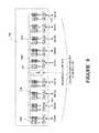
- FIG. 5illustrates a six-rank, one-third width R-DIMM built using x8 DRAM circuits, in accordance with another embodiment.
- FIG. 6illustrates a four-rank, half-width R-DIMM built using x4 DRAM circuits and buffer circuits, in accordance with yet another embodiment.
- FIG. 7illustrates an electronic host system that includes a memory controller, and two half width R-DIMMs, in accordance with another embodiment.
- FIG. 8illustrates an electronic host system that includes a memory controller, and three one-third width R-DIMMs, in accordance with another embodiment.
- FIG. 9illustrates a two-full-rank, half-width R-DIMM built using x8 DRAM circuits and buffer circuits, in accordance with one embodiment.
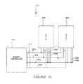
- FIG. 10illustrates an electronic host system that includes a memory controller, and two half width R-DIMMs, in accordance with one embodiment.
- FIG. 1Ashows a system 170 for multi-rank, partial width memory modules, in accordance with one embodiment.
- a memory controller 172is provided. Additionally, a memory bus 174 is provided. Further, a memory module 176 with a plurality of ranks of memory circuits 178 is provided, the memory module 176 including a first number of data pins that is less than a second number of data pins of the memory bus.
- a rankrefers to at least one circuit that is controlled by a common control signal.
- the number of ranks of memory circuits 178may vary.
- the memory module 176may include at least four ranks of memory circuits 178 .
- the memory module 176may include six ranks of memory circuits 178 .
- first number and the second number of data pinsmay vary.
- the first number of data pinsmay be half of the second number of data pins.
- the first number of data pinsmay be a third of the second number of data pins.
- the first number and the second numbermay be any number of data pins such that the first number of data pins is less than the second number of data pins.
- a memory controllerrefers to any device capable of sending instructions or commands, or otherwise controlling the memory circuits 178 .
- a memory busrefers to any component, connection, or group of components and/or connections, used to provide electrical communication between a memory module and a memory controller.
- the memory bus 174may include printed circuit board (PCB) transmission lines, module connectors, component packages, sockets, and/or any other components or connections that fit the above definition.
- PCBprinted circuit board
- the memory circuits 178may include any type of memory device.
- the memory circuits 178may include dynamic random access memory (DRAM).
- the memory module 176may include a dual in-line memory module (DIMM).
- the system 170may include at least one buffer chip (not shown) that is in communication with the memory circuits 178 and the memory bus 174 .
- the buffer chipmay be utilized to transform data signals associated with the memory bus 174 .
- the data signalsmay be transformed from a first data rate to a second data rate which is two times the first data rate.
- data in the data signalsmay be transformed from a first data width to a second data width which is half of the first data width.
- the data signalsmay be associated with data transmission lines included in the memory bus 174 .
- the memory module 176may be connected only some of a plurality of the data transmission lines corresponding to the memory bus. In another embodiment, the memory module 176 may be configured to connect to all of the data transmission lines corresponding to the memory bus.
- FIG. 1Billustrates a two-rank registered DIMM (R-DIMM) 100 built with 8-bit wide (x8) memory (e.g. DRAM, etc.) circuits in accordance with Joint Electron Device Engineering Council (JEDEC) specifications.
- JEDECJoint Electron Device Engineering Council
- the R-DIMM 100may be in communication with a memory controller of an electronic host system as shown.
- a memory controller of an electronic host systemmay be in the form of a desktop computer, a lap-top computer, a server, a storage system, a networking system, a workstation, a personal digital assistant (PDA), a mobile phone, a television, a computer peripheral (e.g. printer, etc.), a consumer electronics system, a communication system, and/or any other software and/or hardware, for that matter.
- PDApersonal digital assistant
- the DRAM circuits 104belong to a first rank and are controlled by a common first chip select signal 140 .
- the DRAM circuits 106belong to a second rank and are controlled by a common second chip select signal 150 .
- the memory controllermay access the first rank by placing an address and command on the address and control lines 120 and asserting the first chip select signal 140 .
- datamay then be transferred between the memory controller and the DRAM circuits 104 of the first rank over the data signals 130 .
- the data signals 130represent all the data signals in the memory bus, and the DRAM circuits 104 connect to all of the data signals 130 .
- the DRAM circuits 104may provide all the data signals requested by the memory controller during a read operation to the first rank, and accept all the data signals provided by the memory controller during a write operation to the first rank.
- the memory busmay have 72 data signals, in which case, each rank on a standard R-DIMM may have nine x8 DRAM circuits.
- the memory controllermay also access the second rank by placing an address and command on the address and control lines 120 and asserting the second chip select signal 150 .
- datamay then be transferred between the memory controller and the DRAM circuits 106 of the second rank over the data signals 130 .
- the data signals 130represent all the data signals in the memory bus, and the DRAM circuits 106 connect to all of the data signals 130 .
- the DRAM circuits 106may provide all the data signals requested by the memory controller during a read operation to the second rank, and accept all the data signals provided by the memory controller during a write operation to the second rank.
- FIG. 2illustrates a two-rank registered DIMM (R-DIMM) 200 built with 4-bit wide (x4) DRAM circuits in accordance with JEDEC specifications. Again, the aforementioned definitions may apply during the present description.
- a register chip 202As shown, included are a register chip 202 , and a plurality of DRAM circuits 204 A, 204 B, 206 A, and 206 B.
- the R-DIMM 200may be in communication with a memory controller of an electronic host system as shown.
- the DRAM circuits 204 A and 204 Bbelong to a first rank and are controlled by a common first chip select signal 240 .
- the DRAM circuits 2044may be positioned on one side of the R-DIMM 200 while the DRAM circuits 204 B are positioned on the opposite side of the R-DIMM 200 .
- the DRAM circuits 206 A and 206 Bbelong to a second rank and are controlled by a common second chip select signal 250 .
- the DRAM circuits 206 Amay be positioned on one side of the R-DIMM 200 while the DRAM circuits 206 B are positioned on the opposite side of the R-DIMM 200 .
- the DRAM circuits 204 A and 206 Amay be stacked on top of each other, or placed next to each other on the same side of a DIMM PCB, or placed on opposite sides of the DIMM PCB in a clamshell-type arrangement.
- the DRAM circuits 204 B and 206 Bmay be stacked on top of each other, or placed next to each other on the same side of the DIMM PCB, or placed on opposite sides of the board in a clamshell-type arrangement.
- the memory controllermay access the first rank by placing an address and command on address and control lines 220 and asserting a first chip select signal 240 .
- datamay then be transferred between the memory controller and the DRAM circuits 204 A and 204 B of the first rank over the data signals 230 .
- the data signals 230represent all the data signals in the memory bus, and the DRAM circuits 204 A and 204 B connect to all of the data signals 230 .
- the memory controllermay also access the second rank by placing an address and command on the address and control lines 220 and asserting a second chip select signal 250 .
- datamay then be transferred between the memory controller and the DRAM circuits 206 A and 206 B of the second rank over the data signals 230 .
- the data signals 230represent all the data signals in the memory bus, and the DRAM circuits 206 A and 206 B connect to all of the data signals in the memory bus. For example, if the memory bus has 72 data signals, each rank of a standard R-DIMM will have eighteen x4 DRAM circuits.
- FIG. 3illustrates an electronic host system 300 that includes a memory controller 350 , and two standard R-DIMMs 330 and 340 . Additionally, the aforementioned definitions may apply during the present description.
- a parallel memory bus 310connects the memory controller 350 to the two standard R-DIMMs 330 and 340 , each of which is a two rank DIMM.
- the memory bus 310includes an address bus 312 , a control bus 314 , a data bus 316 , and clock signals 318 . All the signals in the address bus 312 and the data bus 316 connect to both of the R-DIMMs 330 and 340 while some, but not all, of the signals in the control bus 314 connect to of the R-DIMMs 330 and 340 .
- the control bus 314includes a plurality of chip select signals.
- the first two of these signals, 320 and 322connect to the first R-DIMM 330
- the third and fourth chip select signals, 324 and 326connect to the second R-DIMM 340 .
- the memory controller 350accesses the first rank of DRAM circuits, it asserts chip select signal 320 and the corresponding DRAM circuits on the R-DIMM 330 respond to the access.
- the memory controller 350wishes to access the third rank of DRAM circuits, it asserts chip select signal 324 and the corresponding DRAM circuits on the R-DIMM 340 respond to the access.
- each memory accessinvolves DRAM circuits on only one R-DIMM.
- both of the R-DIMMs 330 and 340connect to the data bus 316 in parallel.
- any given accessinvolves one source and two loads.
- the memory controller 350writes data to a rank of DRAM circuits on the first R-DIMM 330
- both of the R-DIMMs 330 and 340appear as loads to the memory controller 350 .
- a rank of DRAM circuits on the first R-DIMM 330return data (e.g. in a read access) to the memory controller 350
- both the memory controller 350 and the second R-DIMM 340appear as loads to the DRAM circuits on the first R-DIMM 330 that are driving the data bus 316 .
- Topologies that involve a source and multiple loadsare typically capable of operating at lower speeds than point-to-point topologies that have one source and one load.
- FIG. 4illustrates a four-rank, half-width R-DIMM 400 built using x4 DRAM circuits, in accordance with one embodiment.
- the R-DIMM 400may be implemented in the context of the details of FIGS. 1-3 .
- the R-DIMM 400may be implemented in any desired environment. Again, the aforementioned definitions may apply during the present description.
- a register chip 402included in a register chip 402 , and a plurality of DRAM circuits 404 , 406 , 408 , and 410 .
- the DRAM circuits 404belong to the first rank and are controlled by a common chip select signal 420 .
- the DRAM circuits 406belong to the second rank and are controlled by a chip select signal 430 .
- the DRAM circuits 408belong to the third rank and are controlled by a chip select signal 440
- the DRAM circuits 410belong to the fourth rank and are controlled by a chip select signal 450 .
- the DRAM circuits 404 , 406 , 408 , and 410are all x4 DRAM circuits, and are grouped into nine sets of DRAM circuits. Each set contains one DRAM circuit from each of the four ranks. The data pins of the DRAM circuits in a set are connected to each other and to four data pins 470 of the R-DIMM 400 . Since there are nine such sets, the R-DIMM 400 may connect to 36 data signals of a memory bus. In the case where a typical memory bus has 72 data signals, the R-DIMM 400 is a halts-width DIMM with four ranks of DRAM circuits.
- FIG. 5illustrates a six-rank, one-third width R-DIMM 500 built using x8 DRAM circuits, in accordance with another embodiment.
- the R-DIMM 500may be implemented in the context of the details of FIGS. 1-4 .
- the R-DIMM 500may be implemented in any desired environment. Additionally, the aforementioned definitions may apply during the present description.
- a register chip 502and a plurality of DRAM circuits 504 , 506 , 508 , 510 , 512 , and 514 .
- the DRAM circuits 504belong to the first rank and are controlled by a common chip select signal 520 .
- the DRAM circuits 506belong to the second rank and are controlled by a chip select signal 530 .
- the DRAM circuits 508belong to the third rank and are controlled by a chip select signal 540
- the DRAM circuits 510belong to the fourth rank and are controlled by a chip select signal 550 .
- the DRAM circuits 512belong to the fifth rank and are controlled by a chip select signal 560 .
- the DRAM circuits 514belong to the sixth rank and are controlled by a chip select signal 570 .
- the DRAM circuits 504 , 506 , 508 , 510 , 512 , and 514are all x8 DRAM circuits, and are grouped into three sets of DRAM circuits. Each set contains one DRAM circuit from each of the six ranks. The data pins of the DRAM circuits in a set are connected to each other and to eight data pins 590 of the R-DIMM 500 . Since there are three such sets, the R-DIMM 500 may connect to 24 data signals of a memory bus. In the ease where a typical memory bus has 72 data signals, the R-DIMM 500 is a one-third width DIMM with six ranks of DRAM circuits.
- FIG. 6illustrates a four-rank, half-width R-DIMM 600 built using x4 DRAM circuits and buffer circuits, in accordance with yet another embodiment.
- the R-DIMM 600may be implemented in the context of the details of FIGS. 1-5 .
- the R-DIMM 600may be implemented in any desired environment. Again, the aforementioned definitions may apply during the present description.
- a register chip 602included in a register chip 602 , a plurality of DRAM circuits 604 , 606 , 608 , and 610 , and buffer circuits 612 .
- the DRAM circuits 604belong to the first rank and are controlled by a common chip select signal 620 .
- the DRAM circuits 606belong to the second rank and are controlled by a chip select signal 630 .
- the DRAM circuits 608belong to the third rank and are controlled by a chip select signal 640 .
- the DRAM circuits 610belong to the fourth rank and are controlled by a chip select signal 650 .
- the DRAM circuits 604 , 606 , 608 , and 610are all x4 DRAM circuits, and are grouped into nine sets of DRAM circuits. Each set contains one DRAM circuit from each of the four ranks, and in one embodiment, the buffer chip 612 .
- the data pins of the DRAM circuits 604 , 606 , 608 , and 610 in a setare connected to a first set of pins of the buffer chip 612 , while a second set of pins of the buffer chip 612 are connected to four data pins 670 of the R-DIMM 600 .
- the buffer chip 612reduces the loading of the multiple ranks of DRAM circuits on the data bus since each data pin of the R-DIMM 600 connects to only one pin of a buffer chip instead of the corresponding data pin of four DRAM circuits.
- each of the DRAM circuit 604 , 606 , 608 , and 610may be a plurality of DRAM circuits that are emulated by the buffer chip to appear as a higher capacity virtual DRAM circuit to the memory controller with at least one aspect that is different from that of the plurality of DRAM circuits.
- such aspectmay include, for example, a number, a signal, a memory capacity, a timing, a latency, a design parameter, a logical interface, a control system, a property, a behavior (e.g. power behavior), and/or any other aspect, for that matter.
- Such embodimentsmay, for example, enable higher capacity, multi-rank, partial width DIMMs.
- the address and control signals on the R-DIMM 600are not shown in FIG. 6 .
- FIG. 7illustrates an electronic host system 700 that includes a memory controller 750 , and two half width R-DIMMs 730 and 740 , in accordance with another embodiment.
- the electronic host system 700may be implemented in the context of the details of FIGS. 1-6 .
- the electronic host system 700may be implemented in any desired environment. Additionally, the aforementioned definitions may apply during the present description.
- a parallel memory bus 710connects the memory controller 750 to the two half width R-DIMMs 730 and 740 , each of which is a four-rank DIMM.
- the memory busincludes an address bus 712 , a control bus 714 , a data bus 116 , and clock signals 718 . All the signals in the address bus 712 connect to both of the R-DIMMs 730 and 740 while only half the signals in the data bus 716 connect to each R-DIMM 730 and 740 .
- the control bus 714includes a plurality of chip select signals.
- the chip select signals corresponding to the four ranks in the system, 720 , 722 , 724 , and 726connect to the R-DIMM 730 and to the R-DIMM 740 .
- the memory controller 750accesses the first rank of DRAM circuits, it asserts the chip select signal 720 and the corresponding DRAM circuits on the R-DIMM 730 and on the R-DIMM 740 respond to the access.
- the memory controller 750performs a read access to the first rank of DRAM circuits, half the data signals are driven by DRAM circuits on the R-DIMM 730 while the other half of the data signals are driven by DRAM circuits on the R-DIMM 740 .
- each memory accessinvolves DRAM circuits on both the R-DIMM 730 and the R-DIMM 740 .
- Such an arrangementtransforms each of the data signals in the data bus 716 into a point-to-point signal between the memory controller 750 and one R-DIMM.
- partial width DIMMsmay be compatible with systems that are configured with traditional parallel memory bus topologies. In other words, all the data signals in the data bus 716 may be connected to the connectors of both DIMMs. However, when partial width DIMMs are used, the memory circuits on each DIMM connect to only half the data signals in the data bus.
- some of the data signals in the data bus 716may be point-to-point nets (i.e. without stubs) while other signals in the data bus 716 may have stubs.
- all the signals in data bus 716connect to the connectors of R-DIMM 730 and R-DIMM 740 .
- the data signals in the data bus 716 that are driven by the DRAM circuits on the R-DIMM 740are point-to-point nets since the memory controller 750 and the DRAM circuits on the R-DIMM 740 are located at either ends of the nets.
- the data signals that are driven by the DRAM circuits on the R-DIMM 730may have stubs since the DRAM circuits on the R-DIMM 730 are not located at one end of the nets.
- the stubscorrespond to the segments of the nets between the two connectors.
- the data signals in the data bus 716 that are driven by the DRAM circuits on the R-DIMM 730may be terminated at the far end of the bus away from the memory controller 750 .
- These termination resistorsmay be located on the motherboard, or on the R-DIMM 740 , or in another suitable place.
- each data signal in the data bus 716connects to only one DIMM connector on the memory bus 710 .
- FIG. 8illustrates an electronic host system 800 that includes a memory controller 840 , and three one-third width R-DIMMs 850 , 860 , and 870 , in accordance with another embodiment.
- the electronic host system 800may be implemented in the context of the details of FIGS. 1-7 .
- the electronic host system 800may be implemented in any desired environment. Still yet, the aforementioned definitions may apply during the present description.
- a parallel memory bus 880connects the memory controller 840 to the three one-third width R-DIMMs 850 , 860 , and 870 , each of which is a six-rank DIMM.
- the memory bus 880includes an address but (not shown), a control bus 814 , a data bus 812 , and clock signals (not shown). All the signals in the address bus connect to all three R-DIMMs while only one-third of the signals in the data bus 812 connect to each of the R-DIMMs 850 , 860 , and 870 .
- the control bus 814includes a plurality of chip select signals.
- the chip select signals corresponding to the six ranks in the system, 820 , 822 , 824 , 826 , 828 , and 830connect to all three of the R-DIMMs 850 , 860 , and 870 .
- the memory controller 840accesses the first rank of DRAM circuits, it asserts the chip select signal 820 and the corresponding DRAM circuits on the R-DIMM 850 , on the R-DIMM 860 , and on the R-DIMM 870 respond to the access.
- each memory accessinvolves DRAM circuits on all three of the R-DIMMs 850 , 860 , and 870 .
- Such an arrangementtransforms each of the data signals in the data bus 812 into a point-to-point signal between the memory controller 840 and one R-DIMM.
- partial-rank, partial width, memory modulesmay be provided, wherein each DIMM corresponds to a part of all of the ranks in the memory bus.
- each DIMMconnects to some but not all of the data signals in a memory bus for all of the ranks in the channel.
- each R-DIMMmay have two ranks and connect to all 72 data signals in the channel. Therefore, each data signal in the memory bus is connected to the memory controller and the two R-DIMMs.
- each R-DIMMmay have four ranks but the first R-DIMM may connect to 36 data signals in the channel while the second R-DIMM may connect to the other 36 data signals in the channel.
- each of the data signal in the memory busbecomes a point-to-point connection between the memory controller and one R-DIMM, which reduces signal integrity issues and increases the maximum frequency of operation of the channel.
- full-rank, partial width, memory modulesmay be built that correspond to one or more complete ranks but connect to some but not all of the data signals in the memory bus.
- FIG. 9illustrates a two-full-rank, half-width R-DIMM 900 built using x8 DRAM circuits and buffer circuits, in accordance with one embodiment.
- the R-DIMM 900may be implemented in the context of the details of FIGS. 1-8 .
- the R-DIMM 900may be implemented in any desired environment. Again, the aforementioned definitions may apply during the present description.
- a register chip 902included in a register chip 902 , a plurality of DRAM circuits 904 and 906 , and buffer circuits 912 .
- the DRAM circuits 904belong to the first rank and are controlled by a common chip select signal 920 .
- the DRAM circuits 906belong to the second rank and are controlled by chip select signal 930 .
- the DRAM circuits 904 and 906are all illustrated as x8 DRAM circuits, and are grouped into nine sets of DRAM circuits. Each set contains one DRAM circuit from each of the two ranks, and in one embodiment, the buffer chip 912 .
- the eight data pins of each of the DRAM circuits in a setare connected to a first set of pins of the buffer chip 912 , while a second set of pins of the buffer chip 912 are connected to four data pins 970 of the R-DIMM 900 .
- the buffer chip 912acts to transform the eight data signals from each DRAM circuit operating at a specific data rate to four data signals that operate at twice the data rate and connect to the data pins of the R-DIMM, and vice versa. Since there are nine such sets, the R-DIMM 900 may connect to 36 data signals of a memory bus.
- each DRAM circuit 904 and 906may be a plurality of DRAM circuits that are emulated by the buffer chip to appear as a higher capacity virtual DRAM circuit to the memory controller with at least one aspect that is different from that of the plurality of DRAM circuits.
- such aspectmay include, for example, a number, a signal, a memory capacity, a timing, a latency, a design parameter, a logical interface, a control system, a property, a behavior (e.g. power behavior), and/or any other aspect, for that matter.
- Such embodimentsmay, for example, enable higher capacity, full-rank, partial width DIMMs.
- the address and control signals on the R-DIMM 900are not shown in FIG. 9 .
- FIG. 10illustrates an electronic host system 1000 that includes a memory controller 1050 , and two half width R-DIMMs 1030 and 1040 , in accordance with one embodiment.
- the electronic, host system 1000may be implemented in the context of the details of FIGS. 1-9 .
- the electronic host system 1000may be implemented in any desired environment. Additionally, the aforementioned definitions may apply during the present description.
- a parallel memory bus 1010connects the memory controller 1050 to the two half width R-DIMMs 1030 and 1040 , each of which is a two-rank R-DIMM.
- the memory bus 1010includes an address bus 1012 , a control bus 1014 , and a data bus 1016 , and clock signals 1018 . All the signals in the address bus 1012 connect to both of the R-DIMMs 1030 and 1040 while only half the signals in the data bus 1016 connect to each R-DIMM.
- the control bus 1014includes a plurality of chip select signals.
- the chip select signals corresponding to the first two ranks, 1020 and 1022connect to the R-DIMM 1030 while chip select signals corresponding to the third and fourth ranks, 1024 and 1026 , connect to the R-DIMM 1040 .
- the memory controller 1050accesses the first rank of DRAM circuits, it asserts chip select signal 1020 and the corresponding DRAM circuits on the R-DIMM 1030 respond to the access.
- the R-DIMM 1030provides the entire read data on half the data signals in the data bus but at twice the operating speed of the DRAM circuits on the R-DIMM 1030 .
- the DRAM circuits on the R-DIMM 1030 that are controlled by chip select signal 1020will return n 72-bit wide data words at a speed of f transactions per second.
- the buffer circuits on the R-DIMM 1030will transform the read data in 2n 36-bit wide data words and drive them to the memory controller 1050 at a speed of 2f transactions per second.
- the memory controller 1050will then convert the 2n 36-bit wide data words coming in at 2f transactions per second back to n 72-bit wide data words at f transactions per second. It should be noted that the remaining 36 data signal lines in the data bus 1016 that are connected to the R-DIMM 1040 are not driven during this read operation.
- each memory accessinvolves DRAM circuits on only one R-DIMM.
- Such an arrangementtransforms each of the data signals in the data bus 1016 into a point-to-point signal between the memory controller 1050 and one R-DIMM.
- full-rank, partial width DIMMsmay be compatible with systems that are configured with traditional parallel memory bus topologies.
- all the data signals in the data bus 1016may be connected to the connectors of both of the R-DIMMs 1030 and 1040 .
- each DIMMconnects to only half the data signals in the data bus 1016 .
- some of the data signals in the data bus 1016may be point-to-point nets (i.e. without stubs) while other signals in the data bus 1016 may have stubs.
- the data signals in data bus 1016connect to the connectors of the R-DIMM 1030 and the R-DIMM 1040 .
- the data signals in the data bus that are driven by the R-DIMM 1040are point-to-point nets since the memory controller 1050 and the buffer circuits on the R-DIMM 1040 are located at either ends of the nets.
- the data signals that are driven by the R-DIMM 1030may have stubs since the buffer circuits on the R-DIMM 1030 are not located at one end of the nets.
- the stubscorrespond to the segments of the nets between the two connectors.
- the data signals in the data bus that are driven by the R-DIMM 1030may be terminated at the far end of the bus away from the memory controller 1050 .
- These termination resistorsmay be located on the motherboard, or on the R-DIMM 1040 , or in another suitable place.
- the data signals that are driven by the R-DIMM 1040may also be similarly terminated in other embodiments.
- an tin-buffered DIMM(UDIMM), a small outline DIMM (SO-DIMM), a single inline memory module (SIMM), a MiniDIMM, a very low profile (VLP) R-DIMM, etc. may be built to be multi-rank and partial width memory modules.
- three-rank one-third width DIMMsmay be built.
- the memory controller and optional buffer functionsmay be implemented in several ways. As shown here the buffer function is implemented as part of the memory module. The buffer function could also be implemented on the motherboard beside the memory controller, for example.
Landscapes
- Engineering & Computer Science (AREA)
- Theoretical Computer Science (AREA)
- Physics & Mathematics (AREA)
- General Engineering & Computer Science (AREA)
- General Physics & Mathematics (AREA)
- Microelectronics & Electronic Packaging (AREA)
- Dram (AREA)
- Computer Hardware Design (AREA)
Abstract
Description
Claims (20)
Priority Applications (5)
| Application Number | Priority Date | Filing Date | Title |
|---|---|---|---|
| US13/411,489US8446781B1 (en) | 2006-11-13 | 2012-03-02 | Multi-rank partial width memory modules |
| US13/898,002US8760936B1 (en) | 2006-11-13 | 2013-05-20 | Multi-rank partial width memory modules |
| US14/090,342US9171585B2 (en) | 2005-06-24 | 2013-11-26 | Configurable memory circuit system and method |
| US14/922,388US9507739B2 (en) | 2005-06-24 | 2015-10-26 | Configurable memory circuit system and method |
| US15/358,335US10013371B2 (en) | 2005-06-24 | 2016-11-22 | Configurable memory circuit system and method |
Applications Claiming Priority (3)
| Application Number | Priority Date | Filing Date | Title |
|---|---|---|---|
| US86562306P | 2006-11-13 | 2006-11-13 | |
| US11/939,432US8130560B1 (en) | 2006-11-13 | 2007-11-13 | Multi-rank partial width memory modules |
| US13/411,489US8446781B1 (en) | 2006-11-13 | 2012-03-02 | Multi-rank partial width memory modules |
Related Parent Applications (3)
| Application Number | Title | Priority Date | Filing Date |
|---|---|---|---|
| US11/939,432ContinuationUS8130560B1 (en) | 2005-06-24 | 2007-11-13 | Multi-rank partial width memory modules |
| US14/090,432ContinuationUS9952064B2 (en) | 2013-11-26 | 2013-11-26 | Transformer position sensor with shorted coil |
| US14/922,388ContinuationUS9507739B2 (en) | 2005-06-24 | 2015-10-26 | Configurable memory circuit system and method |
Related Child Applications (1)
| Application Number | Title | Priority Date | Filing Date |
|---|---|---|---|
| US13/898,002ContinuationUS8760936B1 (en) | 2005-06-24 | 2013-05-20 | Multi-rank partial width memory modules |
Publications (1)
| Publication Number | Publication Date |
|---|---|
| US8446781B1true US8446781B1 (en) | 2013-05-21 |
Family
ID=45757944
Family Applications (3)
| Application Number | Title | Priority Date | Filing Date |
|---|---|---|---|
| US11/939,432ActiveUS8130560B1 (en) | 2005-06-24 | 2007-11-13 | Multi-rank partial width memory modules |
| US13/411,489Expired - Fee RelatedUS8446781B1 (en) | 2005-06-24 | 2012-03-02 | Multi-rank partial width memory modules |
| US13/898,002ActiveUS8760936B1 (en) | 2005-06-24 | 2013-05-20 | Multi-rank partial width memory modules |
Family Applications Before (1)
| Application Number | Title | Priority Date | Filing Date |
|---|---|---|---|
| US11/939,432ActiveUS8130560B1 (en) | 2005-06-24 | 2007-11-13 | Multi-rank partial width memory modules |
Family Applications After (1)
| Application Number | Title | Priority Date | Filing Date |
|---|---|---|---|
| US13/898,002ActiveUS8760936B1 (en) | 2005-06-24 | 2013-05-20 | Multi-rank partial width memory modules |
Country Status (1)
| Country | Link |
|---|---|
| US (3) | US8130560B1 (en) |
Cited By (15)
| Publication number | Priority date | Publication date | Assignee | Title |
|---|---|---|---|---|
| US8760936B1 (en)* | 2006-11-13 | 2014-06-24 | Google Inc. | Multi-rank partial width memory modules |
| US8908450B1 (en) | 2014-07-21 | 2014-12-09 | I'M Intelligent Memory Limited | Double capacity computer memory device |
| US8930647B1 (en) | 2011-04-06 | 2015-01-06 | P4tents1, LLC | Multiple class memory systems |
| US20150043298A1 (en)* | 2013-08-09 | 2015-02-12 | Renesas Electronics Corporation | Electronic device |
| US9158546B1 (en) | 2011-04-06 | 2015-10-13 | P4tents1, LLC | Computer program product for fetching from a first physical memory between an execution of a plurality of threads associated with a second physical memory |
| US9164679B2 (en) | 2011-04-06 | 2015-10-20 | Patents1, Llc | System, method and computer program product for multi-thread operation involving first memory of a first memory class and second memory of a second memory class |
| US9170744B1 (en) | 2011-04-06 | 2015-10-27 | P4tents1, LLC | Computer program product for controlling a flash/DRAM/embedded DRAM-equipped system |
| US9176671B1 (en) | 2011-04-06 | 2015-11-03 | P4tents1, LLC | Fetching data between thread execution in a flash/DRAM/embedded DRAM-equipped system |
| US9298614B2 (en) | 2014-03-14 | 2016-03-29 | International Business Machines Corporation | Combined rank and linear address incrementing utility for computer memory test operations |
| US9417754B2 (en) | 2011-08-05 | 2016-08-16 | P4tents1, LLC | User interface system, method, and computer program product |
| US10460600B2 (en) | 2016-01-11 | 2019-10-29 | NetraDyne, Inc. | Driver behavior monitoring |
| US11314209B2 (en) | 2017-10-12 | 2022-04-26 | NetraDyne, Inc. | Detection of driving actions that mitigate risk |
| US11322018B2 (en) | 2016-07-31 | 2022-05-03 | NetraDyne, Inc. | Determining causation of traffic events and encouraging good driving behavior |
| US11840239B2 (en) | 2017-09-29 | 2023-12-12 | NetraDyne, Inc. | Multiple exposure event determination |
| US12406576B2 (en) | 2016-01-11 | 2025-09-02 | NetraDyne, Inc. | Driver behavior monitoring |
Families Citing this family (25)
| Publication number | Priority date | Publication date | Assignee | Title |
|---|---|---|---|---|
| US7916574B1 (en) | 2004-03-05 | 2011-03-29 | Netlist, Inc. | Circuit providing load isolation and memory domain translation for memory module |
| US9507739B2 (en) | 2005-06-24 | 2016-11-29 | Google Inc. | Configurable memory circuit system and method |
| US10013371B2 (en) | 2005-06-24 | 2018-07-03 | Google Llc | Configurable memory circuit system and method |
| US9171585B2 (en) | 2005-06-24 | 2015-10-27 | Google Inc. | Configurable memory circuit system and method |
| US8787060B2 (en) | 2010-11-03 | 2014-07-22 | Netlist, Inc. | Method and apparatus for optimizing driver load in a memory package |
| US8154901B1 (en) | 2008-04-14 | 2012-04-10 | Netlist, Inc. | Circuit providing load isolation and noise reduction |
| US8417870B2 (en)* | 2009-07-16 | 2013-04-09 | Netlist, Inc. | System and method of increasing addressable memory space on a memory board |
| US8516185B2 (en)* | 2009-07-16 | 2013-08-20 | Netlist, Inc. | System and method utilizing distributed byte-wise buffers on a memory module |
| JP2010282511A (en)* | 2009-06-05 | 2010-12-16 | Elpida Memory Inc | Memory module and memory system including the same |
| JP2010282510A (en)* | 2009-06-05 | 2010-12-16 | Elpida Memory Inc | Memory module |
| US9128632B2 (en) | 2009-07-16 | 2015-09-08 | Netlist, Inc. | Memory module with distributed data buffers and method of operation |
| JP2012203807A (en)* | 2011-03-28 | 2012-10-22 | Elpida Memory Inc | Memory module |
| JP6006920B2 (en)* | 2011-07-04 | 2016-10-12 | ピーエスフォー ルクスコ エスエイアールエルPS4 Luxco S.a.r.l. | Semiconductor module and module substrate |
| US9703483B2 (en)* | 2012-11-27 | 2017-07-11 | Rambus Inc. | Multiple memory rank system and selection method thereof |
| US10324841B2 (en) | 2013-07-27 | 2019-06-18 | Netlist, Inc. | Memory module with local synchronization |
| WO2015048199A1 (en)* | 2013-09-24 | 2015-04-02 | Rambus Inc. | High capacity memory system |
| EP3058571A1 (en) | 2013-10-15 | 2016-08-24 | Rambus Inc. | Load reduced memory module |
| CN110299157B (en) | 2013-11-11 | 2023-04-28 | 拉姆伯斯公司 | Mass storage system using standard controller components |
| US9697884B2 (en) | 2015-10-08 | 2017-07-04 | Rambus Inc. | Variable width memory module supporting enhanced error detection and correction |
| CN109416656B (en) | 2016-10-31 | 2023-08-11 | 拉姆伯斯公司 | Hybrid memory module |
| TWI708150B (en)* | 2018-05-08 | 2020-10-21 | 華碩電腦股份有限公司 | Motherboard and memory module |
| US20210103533A1 (en)* | 2019-10-04 | 2021-04-08 | Etron Technology, Inc. | Memory system and memory chip |
| KR20240093768A (en)* | 2021-10-22 | 2024-06-24 | 태크염 엘티디. | Layout for dual inline memory to support 128-byte cache line processors |
| CN114758696B (en)* | 2022-04-20 | 2025-06-10 | 芯动微电子科技(珠海)有限公司 | Storage system and method of operating the same |
| US12324102B2 (en)* | 2023-01-26 | 2025-06-03 | SanDisk Technologies, Inc. | Semiconductor storage device including staggered semiconductor memory devices on opposed surfaces |
Citations (623)
| Publication number | Priority date | Publication date | Assignee | Title |
|---|---|---|---|---|
| US3800292A (en) | 1972-10-05 | 1974-03-26 | Honeywell Inf Systems | Variable masking for segmented memory |
| US4069452A (en) | 1976-09-15 | 1978-01-17 | Dana Laboratories, Inc. | Apparatus for automatically detecting values of periodically time varying signals |
| US4323965A (en) | 1980-01-08 | 1982-04-06 | Honeywell Information Systems Inc. | Sequential chip select decode apparatus and method |
| US4334307A (en) | 1979-12-28 | 1982-06-08 | Honeywell Information Systems Inc. | Data processing system with self testing and configuration mapping capability |
| US4345319A (en) | 1978-06-28 | 1982-08-17 | Cselt-Centro Studi E Laboratori Telecomunicazioni S.P.A. | Self-correcting, solid-state-mass-memory organized by bits and with reconfiguration capability for a stored program control system |
| US4392212A (en) | 1979-11-12 | 1983-07-05 | Fujitsu Limited | Semiconductor memory device with decoder for chip selection/write in |
| US4566082A (en) | 1983-03-23 | 1986-01-21 | Tektronix, Inc. | Memory pack addressing system |
| US4592019A (en) | 1983-08-31 | 1986-05-27 | At&T Bell Laboratories | Bus oriented LIFO/FIFO memory |
| US4698748A (en) | 1983-10-07 | 1987-10-06 | Essex Group, Inc. | Power-conserving control system for turning-off the power and the clocking for data transactions upon certain system inactivity |
| US4710903A (en) | 1986-03-31 | 1987-12-01 | Wang Laboratories, Inc. | Pseudo-static memory subsystem |
| US4780843A (en) | 1983-11-07 | 1988-10-25 | Motorola, Inc. | Wait mode power reduction system and method for data processor |
| US4794597A (en) | 1986-03-28 | 1988-12-27 | Mitsubishi Denki Kabushiki Kaisha | Memory device equipped with a RAS circuit |
| US4796232A (en) | 1987-10-20 | 1989-01-03 | Contel Corporation | Dual port memory controller |
| US4807191A (en) | 1988-01-04 | 1989-02-21 | Motorola, Inc. | Redundancy for a block-architecture memory |
| US4841440A (en) | 1983-04-26 | 1989-06-20 | Nec Corporation | Control processor for controlling a peripheral unit |
| US4862347A (en) | 1986-04-22 | 1989-08-29 | International Business Machine Corporation | System for simulating memory arrays in a logic simulation machine |
| US4887240A (en) | 1987-12-15 | 1989-12-12 | National Semiconductor Corporation | Staggered refresh for dram array |
| US4888687A (en) | 1987-05-04 | 1989-12-19 | Prime Computer, Inc. | Memory control system |
| US4899107A (en) | 1988-09-30 | 1990-02-06 | Micron Technology, Inc. | Discrete die burn-in for nonpackaged die |
| US4912678A (en) | 1987-09-26 | 1990-03-27 | Mitsubishi Denki Kabushiki Kaisha | Dynamic random access memory device with staggered refresh |
| US4922451A (en) | 1987-03-23 | 1990-05-01 | International Business Machines Corporation | Memory re-mapping in a microcomputer system |
| US4935734A (en) | 1985-09-11 | 1990-06-19 | Pilkington Micro-Electronics Limited | Semi-conductor integrated circuits/systems |
| US4937791A (en) | 1988-06-02 | 1990-06-26 | The California Institute Of Technology | High performance dynamic ram interface |
| US4956694A (en) | 1988-11-04 | 1990-09-11 | Dense-Pac Microsystems, Inc. | Integrated circuit chip stacking |
| US5025364A (en) | 1987-06-29 | 1991-06-18 | Hewlett-Packard Company | Microprocessor emulation system with memory mapping using variable definition and addressing of memory space |
| US5072424A (en) | 1985-07-12 | 1991-12-10 | Anamartic Limited | Wafer-scale integrated circuit memory |
| US5083266A (en) | 1986-12-26 | 1992-01-21 | Kabushiki Kaisha Toshiba | Microcomputer which enters sleep mode for a predetermined period of time on response to an activity of an input/output device |
| US5193072A (en) | 1990-12-21 | 1993-03-09 | Vlsi Technology, Inc. | Hidden refresh of a dynamic random access memory |
| US5212666A (en) | 1989-07-10 | 1993-05-18 | Seiko Epson Corporation | Memory apparatus having flexibly designed memory capacity |
| US5220672A (en) | 1990-12-25 | 1993-06-15 | Mitsubishi Denki Kabushiki Kaisha | Low power consuming digital circuit device |
| US5241266A (en) | 1992-04-10 | 1993-08-31 | Micron Technology, Inc. | Built-in test circuit connection for wafer level burnin and testing of individual dies |
| US5252807A (en) | 1990-07-02 | 1993-10-12 | George Chizinsky | Heated plate rapid thermal processor |
| US5257233A (en) | 1990-10-31 | 1993-10-26 | Micron Technology, Inc. | Low power memory module using restricted RAM activation |
| US5278796A (en) | 1991-04-12 | 1994-01-11 | Micron Technology, Inc. | Temperature-dependent DRAM refresh circuit |
| US5282177A (en) | 1992-04-08 | 1994-01-25 | Micron Technology, Inc. | Multiple register block write method and circuit for video DRAMs |
| US5332922A (en) | 1990-04-26 | 1994-07-26 | Hitachi, Ltd. | Multi-chip semiconductor package |
| US5369749A (en) | 1989-05-17 | 1994-11-29 | Ibm Corporation | Method and apparatus for the direct transfer of information between application programs running on distinct processors without utilizing the services of one or both operating systems |
| US5384745A (en) | 1992-04-27 | 1995-01-24 | Mitsubishi Denki Kabushiki Kaisha | Synchronous semiconductor memory device |
| US5388265A (en) | 1992-03-06 | 1995-02-07 | Intel Corporation | Method and apparatus for placing an integrated circuit chip in a reduced power consumption state |
| US5390334A (en) | 1990-10-29 | 1995-02-14 | International Business Machines Corporation | Workstation power management by page placement control |
| US5392251A (en) | 1993-07-13 | 1995-02-21 | Micron Semiconductor, Inc. | Controlling dynamic memory refresh cycle time |
| EP0644547A2 (en) | 1993-09-13 | 1995-03-22 | International Business Machines Corporation | Integrated multichip memory module, structure and fabrication |
| US5408190A (en) | 1991-06-04 | 1995-04-18 | Micron Technology, Inc. | Testing apparatus having substrate interconnect for discrete die burn-in for nonpackaged die |
| US5453434A (en) | 1989-11-13 | 1995-09-26 | Allergan, Inc. | N-substituted derivatives of 3R,4R-ethyl-[(1-methyl-1H-imidazol-5-yl)methyl]-2-pyrrolidone |
| US5467455A (en) | 1993-11-03 | 1995-11-14 | Motorola, Inc. | Data processing system and method for performing dynamic bus termination |
| US5483497A (en) | 1993-08-24 | 1996-01-09 | Fujitsu Limited | Semiconductor memory having a plurality of banks usable in a plurality of bank configurations |
| US5498886A (en) | 1991-11-05 | 1996-03-12 | Monolithic System Technology, Inc. | Circuit module redundancy architecture |
| US5502333A (en) | 1994-03-30 | 1996-03-26 | International Business Machines Corporation | Semiconductor stack structures and fabrication/sparing methods utilizing programmable spare circuit |
| US5513135A (en) | 1994-12-02 | 1996-04-30 | International Business Machines Corporation | Synchronous memory packaged in single/dual in-line memory module and method of fabrication |
| US5513339A (en) | 1992-09-30 | 1996-04-30 | At&T Corp. | Concurrent fault simulation of circuits with both logic elements and functional circuits |
| US5519832A (en) | 1992-11-13 | 1996-05-21 | Digital Equipment Corporation | Method and apparatus for displaying module diagnostic results |
| US5526320A (en) | 1994-12-23 | 1996-06-11 | Micron Technology Inc. | Burst EDO memory device |
| US5530836A (en) | 1994-08-12 | 1996-06-25 | International Business Machines Corporation | Method and apparatus for multiple memory bank selection |
| US5550781A (en) | 1989-05-08 | 1996-08-27 | Hitachi Maxell, Ltd. | Semiconductor apparatus with two activating modes of different number of selected word lines at refreshing |
| US5559990A (en) | 1992-02-14 | 1996-09-24 | Advanced Micro Devices, Inc. | Memories with burst mode access |
| US5566344A (en) | 1994-12-20 | 1996-10-15 | National Semiconductor Corporation | In-system programming architecture for a multiple chip processor |
| US5590071A (en) | 1995-11-16 | 1996-12-31 | International Business Machines Corporation | Method and apparatus for emulating a high capacity DRAM |
| US5598376A (en) | 1994-12-23 | 1997-01-28 | Micron Technology, Inc. | Distributed write data drivers for burst access memories |
| US5604714A (en) | 1995-11-30 | 1997-02-18 | Micron Technology, Inc. | DRAM having multiple column address strobe operation |
| US5608262A (en) | 1995-02-24 | 1997-03-04 | Lucent Technologies Inc. | Packaging multi-chip modules without wire-bond interconnection |
| US5610864A (en) | 1994-12-23 | 1997-03-11 | Micron Technology, Inc. | Burst EDO memory device with maximized write cycle timing |
| US5627791A (en) | 1996-02-16 | 1997-05-06 | Micron Technology, Inc. | Multiple bank memory with auto refresh to specified bank |
| US5640364A (en) | 1994-12-23 | 1997-06-17 | Micron Technology, Inc. | Self-enabling pulse trapping circuit |
| US5640337A (en) | 1992-07-10 | 1997-06-17 | Lsi Logic Corp. | Method and apparatus for interim in-situ testing of an electronic system with an inchoate ASIC |
| US5652724A (en) | 1994-12-23 | 1997-07-29 | Micron Technology, Inc. | Burst EDO memory device having pipelined output buffer |
| US5654204A (en) | 1994-07-20 | 1997-08-05 | Anderson; James C. | Die sorter |
| US5661677A (en) | 1996-05-15 | 1997-08-26 | Micron Electronics, Inc. | Circuit and method for on-board programming of PRD Serial EEPROMS |
| US5668773A (en) | 1994-12-23 | 1997-09-16 | Micron Technology, Inc. | Synchronous burst extended data out DRAM |
| US5675549A (en) | 1994-12-23 | 1997-10-07 | Micron Technology, Inc. | Burst EDO memory device address counter |
| US5682354A (en) | 1995-11-06 | 1997-10-28 | Micron Technology, Inc. | CAS recognition in burst extended data out DRAM |
| US5692121A (en) | 1995-04-14 | 1997-11-25 | International Business Machines Corporation | Recovery unit for mirrored processors |
| US5692202A (en) | 1995-12-29 | 1997-11-25 | Intel Corporation | System, apparatus, and method for managing power in a computer system |
| US5717654A (en) | 1995-02-10 | 1998-02-10 | Micron Technology, Inc. | Burst EDO memory device with maximized write cycle timing |
| USRE35733E (en) | 1991-11-26 | 1998-02-17 | Circuit Components Incorporated | Device for interconnecting integrated circuit packages to circuit boards |
| US5721859A (en) | 1994-12-23 | 1998-02-24 | Micron Technology, Inc. | Counter control circuit in a burst memory |
| US5724288A (en) | 1995-08-30 | 1998-03-03 | Micron Technology, Inc. | Data communication for memory |
| US5729504A (en) | 1995-12-14 | 1998-03-17 | Micron Technology, Inc. | Continuous burst edo memory device |
| US5729503A (en) | 1994-12-23 | 1998-03-17 | Micron Technology, Inc. | Address transition detection on a synchronous design |
| US5742792A (en) | 1993-04-23 | 1998-04-21 | Emc Corporation | Remote data mirroring |
| US5748914A (en) | 1995-10-19 | 1998-05-05 | Rambus, Inc. | Protocol for communication with dynamic memory |
| US5752045A (en) | 1995-07-14 | 1998-05-12 | United Microelectronics Corporation | Power conservation in synchronous SRAM cache memory blocks of a computer system |
| US5761703A (en) | 1996-08-16 | 1998-06-02 | Unisys Corporation | Apparatus and method for dynamic memory refresh |
| US5760478A (en) | 1996-08-20 | 1998-06-02 | International Business Machines Corporation | Clock skew minimization system and method for integrated circuits |
| US5781766A (en) | 1996-05-13 | 1998-07-14 | National Semiconductor Corporation | Programmable compensating device to optimize performance in a DRAM controller chipset |
| US5787457A (en) | 1996-10-18 | 1998-07-28 | International Business Machines Corporation | Cached synchronous DRAM architecture allowing concurrent DRAM operations |
| US5798961A (en) | 1994-08-23 | 1998-08-25 | Emc Corporation | Non-volatile memory module |
| US5802555A (en) | 1995-03-15 | 1998-09-01 | Texas Instruments Incorporated | Computer system including a refresh controller circuit having a row address strobe multiplexer and associated method |
| US5802395A (en) | 1996-07-08 | 1998-09-01 | International Business Machines Corporation | High density memory modules with improved data bus performance |
| US5819065A (en) | 1995-06-28 | 1998-10-06 | Quickturn Design Systems, Inc. | System and method for emulating memory |
| US5831833A (en) | 1995-07-17 | 1998-11-03 | Nec Corporation | Bear chip mounting printed circuit board and a method of manufacturing thereof by photoetching |
| US5835435A (en) | 1997-12-02 | 1998-11-10 | Intel Corporation | Method and apparatus for dynamically placing portions of a memory in a reduced power consumtion state |
| US5838165A (en) | 1996-08-21 | 1998-11-17 | Chatter; Mukesh | High performance self modifying on-the-fly alterable logic FPGA, architecture and method |
| US5838177A (en) | 1997-01-06 | 1998-11-17 | Micron Technology, Inc. | Adjustable output driver circuit having parallel pull-up and pull-down elements |
| US5841580A (en) | 1990-04-18 | 1998-11-24 | Rambus, Inc. | Integrated circuit I/O using a high performance bus interface |
| US5845108A (en) | 1995-12-22 | 1998-12-01 | Samsung Electronics, Co., Ltd. | Semiconductor memory device using asynchronous signal |
| US5850368A (en) | 1995-06-01 | 1998-12-15 | Micron Technology, Inc. | Burst EDO memory address counter |
| US5860106A (en) | 1995-07-13 | 1999-01-12 | Intel Corporation | Method and apparatus for dynamically adjusting power/performance characteristics of a memory subsystem |
| US5870347A (en) | 1997-03-11 | 1999-02-09 | Micron Technology, Inc. | Multi-bank memory input/output line selection |
| US5870350A (en) | 1997-05-21 | 1999-02-09 | International Business Machines Corporation | High performance, high bandwidth memory bus architecture utilizing SDRAMs |
| US5872907A (en) | 1991-12-16 | 1999-02-16 | International Business Machines Corporation | Fault tolerant design for identification of AC defects including variance of cycle time to maintain system operation |
| US5875142A (en) | 1997-06-17 | 1999-02-23 | Micron Technology, Inc. | Integrated circuit with temperature detector |
| US5878279A (en) | 1995-08-03 | 1999-03-02 | Sgs-Thomson Microelectronics S.A. | HDLC integrated circuit using internal arbitration to prioritize access to a shared internal bus amongst a plurality of devices |
| US5901105A (en) | 1995-04-05 | 1999-05-04 | Ong; Adrian E | Dynamic random access memory having decoding circuitry for partial memory blocks |
| US5903500A (en) | 1997-04-11 | 1999-05-11 | Intel Corporation | 1.8 volt output buffer on flash memories |
| US5905688A (en) | 1997-04-01 | 1999-05-18 | Lg Semicon Co., Ltd. | Auto power down circuit for a semiconductor memory device |
| US5907512A (en) | 1989-08-14 | 1999-05-25 | Micron Technology, Inc. | Mask write enablement for memory devices which permits selective masked enablement of plural segments |
| US5913072A (en) | 1997-04-08 | 1999-06-15 | Wieringa; Fred | Image processing system in which image processing programs stored in a personal computer are selectively executed through user interface of a scanner |
| US5915167A (en) | 1997-04-04 | 1999-06-22 | Elm Technology Corporation | Three dimensional structure memory |
| US5917758A (en) | 1996-11-04 | 1999-06-29 | Micron Technology, Inc. | Adjustable output driver circuit |
| US5924111A (en) | 1995-10-17 | 1999-07-13 | Huang; Chu-Kai | Method and system for interleaving data in multiple memory bank partitions |
| US5923611A (en) | 1996-12-20 | 1999-07-13 | Micron Technology, Inc. | Memory having a plurality of external clock signal inputs |
| US5926435A (en) | 1996-12-31 | 1999-07-20 | Hyundai Electronics Industries Co., Ltd. | Apparatus for saving power consumption in semiconductor memory devices |
| US5929650A (en) | 1997-02-04 | 1999-07-27 | Motorola, Inc. | Method and apparatus for performing operative testing on an integrated circuit |
| US5943254A (en) | 1995-02-22 | 1999-08-24 | International Business Machines Corporation | Multichip semiconductor structures with consolidated circuitry and programmable ESD protection for input/output nodes |
| US5949254A (en) | 1996-11-26 | 1999-09-07 | Micron Technology, Inc. | Adjustable output driver circuit |
| US5953263A (en) | 1997-02-10 | 1999-09-14 | Rambus Inc. | Synchronous memory device having a programmable register and method of controlling same |
| US5962435A (en) | 1993-12-10 | 1999-10-05 | Hoechst Marion Roussel, Inc. | Method of lowering serum cholesterol levels with 2,6-di-alkyl-4-silyl-phenols |
| US5963429A (en) | 1997-08-20 | 1999-10-05 | Sulzer Intermedics Inc. | Printed circuit substrate with cavities for encapsulating integrated circuits |
| US5963464A (en) | 1998-02-26 | 1999-10-05 | International Business Machines Corporation | Stackable memory card |
| US5966724A (en) | 1996-01-11 | 1999-10-12 | Micron Technology, Inc. | Synchronous memory device with dual page and burst mode operations |
| US5966727A (en) | 1996-07-12 | 1999-10-12 | Dux Inc. | Combination flash memory and dram memory board interleave-bypass memory access method, and memory access device incorporating both the same |
| US5969996A (en) | 1995-04-25 | 1999-10-19 | Hiachi, Ltd. | Semiconductor memory device and memory system |
| US5978304A (en)* | 1998-06-30 | 1999-11-02 | Lsi Logic Corporation | Hierarchical, adaptable-configuration dynamic random access memory |
| US5995424A (en) | 1997-07-16 | 1999-11-30 | Tanisys Technology, Inc. | Synchronous memory test system |
| US5995443A (en) | 1990-04-18 | 1999-11-30 | Rambus Inc. | Synchronous memory device |
| US6001671A (en) | 1996-04-18 | 1999-12-14 | Tessera, Inc. | Methods for manufacturing a semiconductor package having a sacrificial layer |
| US6014339A (en) | 1997-04-03 | 2000-01-11 | Fujitsu Limited | Synchronous DRAM whose power consumption is minimized |
| US6016282A (en) | 1998-05-28 | 2000-01-18 | Micron Technology, Inc. | Clock vernier adjustment |
| US6026050A (en) | 1997-07-09 | 2000-02-15 | Micron Technology, Inc. | Method and apparatus for adaptively adjusting the timing of a clock signal used to latch digital signals, and memory device using same |
| US6029250A (en) | 1998-09-09 | 2000-02-22 | Micron Technology, Inc. | Method and apparatus for adaptively adjusting the timing offset between a clock signal and digital signals transmitted coincident with that clock signal, and memory device and system using same |
| US6034916A (en) | 1997-11-18 | 2000-03-07 | Samsung Electronics Co., Ltd. | Data masking circuits and methods for integrated circuit memory devices, including data strobe signal synchronization |
| US6038673A (en) | 1998-11-03 | 2000-03-14 | Intel Corporation | Computer system with power management scheme for DRAM devices |
| US6044032A (en) | 1998-12-03 | 2000-03-28 | Micron Technology, Inc. | Addressing scheme for a double data rate SDRAM |
| US6047073A (en) | 1994-11-02 | 2000-04-04 | Advanced Micro Devices, Inc. | Digital wavetable audio synthesizer with delay-based effects processing |
| US6047344A (en) | 1997-03-05 | 2000-04-04 | Kabushiki Kaisha Toshiba | Semiconductor memory device with multiplied internal clock |
| US6053948A (en) | 1995-06-07 | 2000-04-25 | Synopsys, Inc. | Method and apparatus using a memory model |
| US6058451A (en) | 1997-12-22 | 2000-05-02 | Emc Corporation | Method and apparatus for refreshing a non-clocked memory |
| US6065092A (en) | 1994-11-30 | 2000-05-16 | Hitachi Micro Systems, Inc. | Independent and cooperative multichannel memory architecture for use with master device |
| US6073223A (en) | 1997-07-21 | 2000-06-06 | Hewlett-Packard Company | Memory controller and method for intermittently activating and idling a clock signal for a synchronous memory |
| US6075744A (en) | 1997-10-10 | 2000-06-13 | Rambus Inc. | Dram core refresh with reduced spike current |
| US6075730A (en) | 1997-10-10 | 2000-06-13 | Rambus Incorporated | High performance cost optimized memory with delayed memory writes |
| US6078546A (en) | 1997-03-18 | 2000-06-20 | Samsung Electronics Co., Ltd. | Synchronous semiconductor memory device with double data rate scheme |
| US6079025A (en) | 1990-06-01 | 2000-06-20 | Vadem | System and method of computer operating mode control for power consumption reduction |
| US6088290A (en) | 1997-08-13 | 2000-07-11 | Kabushiki Kaisha Toshiba | Semiconductor memory device having a power-down mode |
| US6091251A (en) | 1991-06-04 | 2000-07-18 | Wood; Alan G. | Discrete die burn-in for nonpackaged die |
| US6101564A (en) | 1995-08-03 | 2000-08-08 | Sgs-Thomson Microelectronics S.A. | Device for organizing the access to a memory bus |
| US6101612A (en) | 1998-10-30 | 2000-08-08 | Micron Technology, Inc. | Apparatus for aligning clock and data signals received from a RAM |
| US6108795A (en) | 1998-10-30 | 2000-08-22 | Micron Technology, Inc. | Method for aligning clock and data signals received from a RAM |
| USRE36839E (en) | 1995-02-14 | 2000-08-29 | Philips Semiconductor, Inc. | Method and apparatus for reducing power consumption in digital electronic circuits |
| US6111812A (en) | 1999-07-23 | 2000-08-29 | Micron Technology, Inc. | Method and apparatus for adjusting control signal timing in a memory device |
| US6134638A (en) | 1997-08-13 | 2000-10-17 | Compaq Computer Corporation | Memory controller supporting DRAM circuits with different operating speeds |
| US6154370A (en) | 1998-07-21 | 2000-11-28 | Lucent Technologies Inc. | Recessed flip-chip package |
| US6166991A (en) | 1999-11-03 | 2000-12-26 | Cypress Semiconductor Corp. | Circuit, architecture and method for reducing power consumption in a synchronous integrated circuit |
| US6181640B1 (en) | 1997-06-24 | 2001-01-30 | Hyundai Electronics Industries Co., Ltd. | Control circuit for semiconductor memory device |
| US6199151B1 (en) | 1998-06-05 | 2001-03-06 | Intel Corporation | Apparatus and method for storing a device row indicator for use in a subsequent page-miss memory cycle |
| US6208168B1 (en) | 1997-06-27 | 2001-03-27 | Samsung Electronics Co., Ltd. | Output driver circuits having programmable pull-up and pull-down capability for driving variable loads |
| US6216246B1 (en) | 1996-05-24 | 2001-04-10 | Jeng-Jye Shau | Methods to make DRAM fully compatible with SRAM using error correction code (ECC) mechanism |
| US6222739B1 (en) | 1998-01-20 | 2001-04-24 | Viking Components | High-density computer module with stacked parallel-plane packaging |
| US6226709B1 (en) | 1997-10-24 | 2001-05-01 | Compaq Computer Corporation | Memory refresh control system |
| US6226730B1 (en) | 1998-06-05 | 2001-05-01 | Intel Corporation | Achieving page hit memory cycles on a virtual address reference |
| US20010000822A1 (en) | 1998-04-28 | 2001-05-03 | Dell Timothy Jay | Dynamic configuration of memory module using presence detect data |
| US6233192B1 (en) | 1998-03-05 | 2001-05-15 | Sharp Kabushiki Kaisha | Semiconductor memory device |
| US6233650B1 (en) | 1998-04-01 | 2001-05-15 | Intel Corporation | Using FET switches for large memory arrays |
| US6240048B1 (en) | 1999-06-29 | 2001-05-29 | Nec Corporation | Synchronous type semiconductor memory system with less power consumption |
| US20010003198A1 (en) | 1999-11-30 | 2001-06-07 | Chung-Che Wu | Method for timing setting of a system memory |
| US6253278B1 (en)* | 1996-08-15 | 2001-06-26 | Micron Technology, Inc. | Synchronous DRAM modules including multiple clock out signals for increasing processing speed |
| US6252807B1 (en) | 1999-08-06 | 2001-06-26 | Mitsubishi Electric Engineering Company, Limited | Memory device with reduced power consumption when byte-unit accessed |
| US6262938B1 (en) | 1999-03-03 | 2001-07-17 | Samsung Electronics Co., Ltd. | Synchronous DRAM having posted CAS latency and method for controlling CAS latency |
| US20010011322A1 (en) | 1998-06-22 | 2001-08-02 | Patrick F. Stolt | Data strobe for faster data access from a memory array |
| US6274395B1 (en) | 1999-12-23 | 2001-08-14 | Lsi Logic Corporation | Method and apparatus for maintaining test data during fabrication of a semiconductor wafer |
| US6279069B1 (en) | 1996-12-26 | 2001-08-21 | Intel Corporation | Interface for flash EEPROM memory arrays |
| US20010019509A1 (en) | 1999-12-22 | 2001-09-06 | Ari Aho | Memory controller |
| US20010021137A1 (en) | 2000-03-13 | 2001-09-13 | Yasukazu Kai | Dynamic random access memory |
| US20010021106A1 (en) | 1999-01-14 | 2001-09-13 | Rick Weber | Stacked printed circuit board memory module |
| US6295572B1 (en) | 1994-01-24 | 2001-09-25 | Advanced Micro Devices, Inc. | Integrated SCSI and ethernet controller on a PCI local bus |
| US6298426B1 (en) | 1997-12-31 | 2001-10-02 | Intel Corporation | Controller configurable for use with multiple memory organizations |
| US6307769B1 (en) | 1999-09-02 | 2001-10-23 | Micron Technology, Inc. | Semiconductor devices having mirrored terminal arrangements, devices including same, and methods of testing such semiconductor devices |
| US6317381B1 (en) | 1999-12-07 | 2001-11-13 | Micron Technology, Inc. | Method and system for adaptively adjusting control signal timing in a memory device |
| US6317352B1 (en) | 2000-09-18 | 2001-11-13 | Intel Corporation | Apparatus for implementing a buffered daisy chain connection between a memory controller and memory modules |
| US6324120B2 (en) | 1990-04-18 | 2001-11-27 | Rambus Inc. | Memory device having a variable data output length |
| US20010046129A1 (en) | 2000-05-24 | 2001-11-29 | International Business Machines Corporation | Interposer for connecting two substrates and resulting assembly |
| US20010046163A1 (en) | 2000-05-19 | 2001-11-29 | Fujitsu Limited | Memory system and memory controller with reliable data latch operation |
| US6327664B1 (en) | 1999-04-30 | 2001-12-04 | International Business Machines Corporation | Power management on a memory card having a signal processing element |
| US6336174B1 (en) | 1999-08-09 | 2002-01-01 | Maxtor Corporation | Hardware assisted memory backup system and method |
| US20020002662A1 (en) | 1998-07-13 | 2002-01-03 | Olarig Sompong Paul | Method and apparatus for supporting heterogeneous memory in computer systems |
| US6338108B1 (en) | 1997-04-15 | 2002-01-08 | Nec Corporation | Coprocessor-integrated packet-type memory LSI, packet-type memory/coprocessor bus, and control method thereof |
| US6338113B1 (en) | 1998-06-10 | 2002-01-08 | Mitsubishi Denki Kabushiki Kaisha | Memory module system having multiple memory modules |
| US20020004897A1 (en) | 2000-07-05 | 2002-01-10 | Min-Cheng Kao | Data processing apparatus for executing multiple instruction sets |
| US6341347B1 (en) | 1999-05-11 | 2002-01-22 | Sun Microsystems, Inc. | Thread switch logic in a multiple-thread processor |
| JP2002025255A (en) | 2000-07-04 | 2002-01-25 | Hitachi Ltd | Semiconductor storage device |
| US6343019B1 (en) | 1997-12-22 | 2002-01-29 | Micron Technology, Inc. | Apparatus and method of stacking die on a substrate |
| US20020015340A1 (en) | 2000-07-03 | 2002-02-07 | Victor Batinovich | Method and apparatus for memory module circuit interconnection |
| US20020019961A1 (en) | 1998-08-28 | 2002-02-14 | Blodgett Greg A. | Device and method for repairing a semiconductor memory |
| US6353561B1 (en) | 1998-09-18 | 2002-03-05 | Fujitsu Limited | Semiconductor integrated circuit and method for controlling the same |
| US6356500B1 (en) | 2000-08-23 | 2002-03-12 | Micron Technology, Inc. | Reduced power DRAM device and method |
| US6356105B1 (en) | 2000-06-28 | 2002-03-12 | Intel Corporation | Impedance control system for a center tapped termination bus |
| US20020038405A1 (en) | 1998-09-30 | 2002-03-28 | Michael W. Leddige | Method and apparatus for implementing multiple memory buses on a memory module |
| US20020041507A1 (en) | 2000-10-10 | 2002-04-11 | Woo Steven C. | Methods and systems for reducing heat flux in memory systems |
| US6381668B1 (en) | 1997-03-21 | 2002-04-30 | International Business Machines Corporation | Address mapping for system memory |
| US6381188B1 (en) | 1999-01-12 | 2002-04-30 | Samsung Electronics Co., Ltd. | DRAM capable of selectively performing self-refresh operation for memory bank |
| US20020051398A1 (en) | 2000-09-12 | 2002-05-02 | Seiko Epson Corporation | Semiconductor device, method for refreshing the same, system memory, and electronics apparatus |
| US6389514B1 (en) | 1999-03-25 | 2002-05-14 | Hewlett-Packard Company | Method and computer system for speculatively closing pages in memory |
| US6392304B1 (en) | 1998-11-12 | 2002-05-21 | United Memories, Inc. | Multi-chip memory apparatus and associated method |
| US20020060948A1 (en) | 2000-11-21 | 2002-05-23 | Nai-Shung Chang | Clock device for supporting multiplicity of memory module types |
| US20020060945A1 (en) | 2000-11-20 | 2002-05-23 | Fujitsu Limited | Synchronous semiconductor device and method for latching input signals |
| US20020064073A1 (en) | 2000-11-30 | 2002-05-30 | Pien Chien | Dram module and method of using sram to replace damaged dram cell |
| US20020064083A1 (en) | 2000-11-24 | 2002-05-30 | Ryu Dong-Ryul | Clock generating circuits controlling activation of a delay locked loop circuit on transition to a standby mode of a semiconductor memory device and methods for operating the same |
| US6414868B1 (en) | 1999-06-07 | 2002-07-02 | Sun Microsystems, Inc. | Memory expansion module including multiple memory banks and a bank control circuit |
| US20020089970A1 (en) | 1998-01-08 | 2002-07-11 | Kabushiki Kaisha Toshiba | Multimedia private branch exchanger and private branch exchange system |
| US6421754B1 (en) | 1994-12-22 | 2002-07-16 | Texas Instruments Incorporated | System management mode circuits, systems and methods |
| US20020094671A1 (en) | 1996-03-07 | 2002-07-18 | Distefano Thomas H. | Methods for providing void-free layers for semiconductor assemblies |
| JP3304893B2 (en) | 1994-06-28 | 2002-07-22 | 日本電気株式会社 | Memory selection circuit and semiconductor memory device |
| US6424532B2 (en) | 1998-06-12 | 2002-07-23 | Nec Corporation | Heat sink and memory module with heat sink |
| US6430103B2 (en) | 2000-02-03 | 2002-08-06 | Hitachi, Ltd. | Semiconductor integrated circuit device with memory banks and read buffer capable of storing data read out from one memory bank when data of another memory bank is outputting |
| US6429029B1 (en) | 1997-01-15 | 2002-08-06 | Formfactor, Inc. | Concurrent design and subsequent partitioning of product and test die |
| US6438057B1 (en) | 2001-07-06 | 2002-08-20 | Infineon Technologies Ag | DRAM refresh timing adjustment device, system and method |
| US6442698B2 (en) | 1998-11-04 | 2002-08-27 | Intel Corporation | Method and apparatus for power management in a memory subsystem |
| US6445591B1 (en) | 2000-08-10 | 2002-09-03 | Nortel Networks Limited | Multilayer circuit board |
| US20020121650A1 (en) | 2001-03-01 | 2002-09-05 | Masanori Minamio | Resin-encapsulated semiconductor device and method for manufacturing the same |
| US20020121670A1 (en) | 2001-03-01 | 2002-09-05 | Matsushita Electric Industrial Co., Ltd. | Lead frame |
| US20020129204A1 (en) | 2001-03-06 | 2002-09-12 | Lance Leighnor | Hypercache RAM based disk emulation and method |
| US6453434B2 (en) | 1998-10-02 | 2002-09-17 | International Business Machines Corporation | Dynamically-tunable memory controller |
| US6453402B1 (en) | 1999-07-13 | 2002-09-17 | Micron Technology, Inc. | Method for synchronizing strobe and data signals from a RAM |
| US6453400B1 (en) | 1997-09-16 | 2002-09-17 | Nec Corporation | Semiconductor integrated circuit device |
| US6455348B1 (en) | 1998-03-12 | 2002-09-24 | Matsushita Electric Industrial Co., Ltd. | Lead frame, resin-molded semiconductor device, and method for manufacturing the same |
| US6457095B1 (en) | 1999-12-13 | 2002-09-24 | Intel Corporation | Method and apparatus for synchronizing dynamic random access memory exiting from a low power state |
| US6459651B1 (en) | 2000-09-16 | 2002-10-01 | Samsung Electronics Co., Ltd. | Semiconductor memory device having data masking pin and memory system including the same |
| US6473831B1 (en) | 1999-10-01 | 2002-10-29 | Avido Systems Corporation | Method and system for providing universal memory bus and module |
| US6476476B1 (en) | 2001-08-16 | 2002-11-05 | Amkor Technology, Inc. | Integrated circuit package including pin and barrel interconnects |
| US20020165706A1 (en) | 2001-05-03 | 2002-11-07 | Raynham Michael B. | Memory controller emulator |
| US6480929B1 (en) | 1998-10-31 | 2002-11-12 | Advanced Micro Devices Inc. | Pseudo-concurrency between a volatile memory and a non-volatile memory on a same data bus |
| US20020167092A1 (en) | 2001-05-08 | 2002-11-14 | Fee Setho Sing | Interposer, packages including the interposer, and methods |
| US20020172024A1 (en) | 2001-05-21 | 2002-11-21 | Hui Chong Chin | Method for encapsulating intermediate conductive elements connecting a semiconductor die to a substrate and semiconductor devices so packaged |
| US20020174274A1 (en) | 2001-05-15 | 2002-11-21 | Wu Kun Ho | DDR and QDR converter and interface card, motherboard and memory module interface using the same |
| US6489669B2 (en) | 2000-09-11 | 2002-12-03 | Rohm Co., Ltd. | Integrated circuit device |
| US6490161B1 (en) | 2002-01-08 | 2002-12-03 | International Business Machines Corporation | Peripheral land grid array package with improved thermal performance |
| US20020184438A1 (en) | 2001-05-31 | 2002-12-05 | Fujitsu Limited | Memory control system |
| US6492726B1 (en) | 2000-09-22 | 2002-12-10 | Chartered Semiconductor Manufacturing Ltd. | Chip scale packaging with multi-layer flip chip arrangement and ball grid array interconnection |
| US6493789B2 (en) | 1995-10-19 | 2002-12-10 | Rambus Inc. | Memory device which receives write masking and automatic precharge information |
| US6496440B2 (en) | 1999-03-01 | 2002-12-17 | Micron Technology, Inc. | Method and system for accessing rows in multiple memory banks within an integrated circuit |
| US6498766B2 (en) | 2000-05-22 | 2002-12-24 | Samsung Electronics Co., Ltd. | Integrated circuit memory devices that utilize indication signals to increase reliability of reading and writing operations and methods of operating same |
| US20030002262A1 (en) | 2001-07-02 | 2003-01-02 | Martin Benisek | Electronic printed circuit board having a plurality of identically designed, housing-encapsulated semiconductor memories |
| US20030011993A1 (en) | 2001-06-28 | 2003-01-16 | Intel Corporation | Heat transfer apparatus |
| US6510097B2 (en) | 2001-02-15 | 2003-01-21 | Oki Electric Industry Co., Ltd. | DRAM interface circuit providing continuous access across row boundaries |
| US6510503B2 (en) | 1998-07-27 | 2003-01-21 | Mosaid Technologies Incorporated | High bandwidth memory interface |
| US20030016550A1 (en) | 2001-07-20 | 2003-01-23 | Yoo Chang-Sik | Semiconductor memory systems, methods, and devices for controlling active termination |
| US6512392B2 (en) | 1998-04-17 | 2003-01-28 | International Business Machines Corporation | Method for testing semiconductor devices |
| US20030021175A1 (en) | 2001-07-27 | 2003-01-30 | Jong Tae Kwak | Low power type Rambus DRAM |
| US20030026155A1 (en) | 2001-08-01 | 2003-02-06 | Mitsubishi Denki Kabushiki Kaisha | Semiconductor memory module and register buffer device for use in the same |
| US20030026159A1 (en) | 2001-07-31 | 2003-02-06 | Infineon Technologies North America Corp. | Fuse programmable I/O organization |
| US6521984B2 (en) | 2000-11-07 | 2003-02-18 | Mitsubishi Denki Kabushiki Kaisha | Semiconductor module with semiconductor devices attached to upper and lower surface of a semiconductor substrate |
| US6526471B1 (en) | 1998-09-18 | 2003-02-25 | Digeo, Inc. | Method and apparatus for a high-speed memory subsystem |
| US6526484B1 (en) | 1998-11-16 | 2003-02-25 | Infineon Technologies Ag | Methods and apparatus for reordering of the memory requests to achieve higher average utilization of the command and data bus |
| US6526473B1 (en) | 1999-04-07 | 2003-02-25 | Samsung Electronics Co., Ltd. | Memory module system for controlling data input and output by connecting selected memory modules to a data line |
| US20030039158A1 (en) | 1998-04-10 | 2003-02-27 | Masashi Horiguchi | Semiconductor device, such as a synchronous dram, including a control circuit for reducing power consumption |
| US20030041295A1 (en) | 2001-08-24 | 2003-02-27 | Chien-Tzu Hou | Method of defects recovery and status display of dram |
| US20030061458A1 (en) | 2001-09-25 | 2003-03-27 | Wilcox Jeffrey R. | Memory control with lookahead power management |
| US20030061459A1 (en) | 2001-09-27 | 2003-03-27 | Nagi Aboulenein | Method and apparatus for memory access scheduling to reduce memory access latency |
| US6553450B1 (en) | 2000-09-18 | 2003-04-22 | Intel Corporation | Buffer to multiply memory interface |
| US6560158B2 (en) | 2001-04-27 | 2003-05-06 | Samsung Electronics Co., Ltd. | Power down voltage control method and apparatus |
| US20030088743A1 (en) | 2001-11-08 | 2003-05-08 | Rader Sheila M. | Mobile wireless communication device architectures and methods therefor |
| US6564285B1 (en) | 1994-06-03 | 2003-05-13 | Intel Corporation | Synchronous interface for a nonvolatile memory |
| US6563337B2 (en) | 2001-06-28 | 2003-05-13 | Intel Corporation | Driver impedance control mechanism |
| US20030093614A1 (en) | 2001-10-22 | 2003-05-15 | Sun Microsystems | Dram power management |
| US20030101392A1 (en) | 2001-11-26 | 2003-05-29 | Lee Chen-Tsai | Method of testing memory with continuous, varying data |
| US6574150B2 (en) | 2000-07-19 | 2003-06-03 | Oki Electric Industry Co., Ltd. | Dynamic random access memory with low power consumption |
| US20030105932A1 (en) | 2001-11-30 | 2003-06-05 | David Howard S. | Emulation of memory clock enable pin and use of chip select for memory power control |
| US20030117875A1 (en) | 2001-12-21 | 2003-06-26 | Lee Kang Seol | Power-up signal generator for semiconductor memory devices |
| US20030126338A1 (en) | 2001-12-31 | 2003-07-03 | Dodd James M. | Memory bus termination with memory unit having termination control |
| US20030123389A1 (en) | 2001-12-31 | 2003-07-03 | Russell Patrick Gene | Apparatus and method for controlling data transmission |
| US6590822B2 (en) | 2001-05-07 | 2003-07-08 | Samsung Electronics Co., Ltd. | System and method for performing partial array self-refresh operation in a semiconductor memory device |
| US20030127737A1 (en) | 2002-01-10 | 2003-07-10 | Norio Takahashi | Semiconductor device |
| US20030131160A1 (en) | 2001-10-22 | 2003-07-10 | Hampel Craig E. | Timing calibration apparatus and method for a memory device signaling system |
| US6594770B1 (en) | 1998-11-30 | 2003-07-15 | Fujitsu Limited | Semiconductor integrated circuit device |
| US6597617B2 (en) | 2000-05-24 | 2003-07-22 | Mitsubishi Denki Kabushiki Kaisha | Semiconductor device with reduced current consumption in standby state |
| US20030145163A1 (en) | 2002-01-25 | 2003-07-31 | Jong-Cheul Seo | Electronic system and refresh method |
| US20030158995A1 (en) | 2002-02-15 | 2003-08-21 | Ming-Hsien Lee | Method for DRAM control with adjustable page size |
| US6614700B2 (en) | 2001-04-05 | 2003-09-02 | Infineon Technologies Ag | Circuit configuration with a memory array |
| US20030164543A1 (en) | 2002-03-04 | 2003-09-04 | Teck Kheng Lee | Interposer configured to reduce the profiles of semiconductor device assemblies and packages including the same and methods |
| US20030164539A1 (en) | 2002-03-01 | 2003-09-04 | Sampson Taiwan Ltd. | Method for stacking semiconductor package units and stacked package |
| US6618267B1 (en) | 1998-09-22 | 2003-09-09 | International Business Machines Corporation | Multi-level electronic package and method for making same |
| US6618791B1 (en) | 2000-09-29 | 2003-09-09 | Intel Corporation | System and method for controlling power states of a memory device via detection of a chip select signal |
| US6621760B1 (en) | 2000-01-13 | 2003-09-16 | Intel Corporation | Method, apparatus, and system for high speed data transfer using source synchronous data strobe |
| US20030182513A1 (en) | 2002-03-22 | 2003-09-25 | Dodd James M. | Memory system with burst length shorter than prefetch length |
| US6628538B2 (en) | 2000-03-10 | 2003-09-30 | Hitachi, Ltd. | Memory module including module data wirings available as a memory access data bus |
| US20030183934A1 (en) | 2002-03-29 | 2003-10-02 | Barrett Joseph C. | Method and apparatus for stacking multiple die in a flip chip semiconductor package |
| US6631086B1 (en) | 2002-07-22 | 2003-10-07 | Advanced Micro Devices, Inc. | On-chip repair of defective address of core flash memory cells |
| US6630729B2 (en) | 2000-09-04 | 2003-10-07 | Siliconware Precision Industries Co., Ltd. | Low-profile semiconductor package with strengthening structure |
| US20030191888A1 (en) | 2002-04-09 | 2003-10-09 | Klein Dean A. | Method and system for dynamically operating memory in a power-saving error correction mode |
| US20030189870A1 (en) | 2002-04-05 | 2003-10-09 | Wilcox Jeffrey R. | Individual memory page activity timing method and system |
| US20030189868A1 (en) | 2002-04-09 | 2003-10-09 | Riesenman Robert J. | Early power-down digital memory device and method |
| US20030191915A1 (en) | 2002-04-09 | 2003-10-09 | Alankar Saxena | Method, system, and apparatus for reducing power consumption of a memory |
| US20030200474A1 (en) | 2002-04-17 | 2003-10-23 | Fujitsu Limited | Clock control apparatus and method for a memory controller |
| US20030200382A1 (en) | 2002-04-18 | 2003-10-23 | Wells Owen Newton | Methods and apparatus for backing up a memory device |
| US20030206476A1 (en) | 2002-05-06 | 2003-11-06 | Micron Technology, Inc. | Low power consumption memory device having row-to-column short |
| US20030205802A1 (en) | 2002-02-20 | 2003-11-06 | Segaram Para Kanagasabai | Method of bonding a semiconductor die without an ESD circuit and a separate ESD circuit to an external lead, and a semiconductor device made thereby |
| US6650594B1 (en) | 2002-07-12 | 2003-11-18 | Samsung Electronics Co., Ltd. | Device and method for selecting power down exit |
| US20030217303A1 (en) | 2002-05-20 | 2003-11-20 | Hitachi, Ltd. | Interface circuit |
| US6658016B1 (en) | 1999-03-05 | 2003-12-02 | Broadcom Corporation | Packet switching fabric having a segmented ring with token based resource control protocol and output queuing control |
| US6657634B1 (en) | 1999-02-25 | 2003-12-02 | Ati International Srl | Dynamic graphics and/or video memory power reducing circuit and method |
| US6657918B2 (en) | 1994-10-06 | 2003-12-02 | Mosaid Technologies Incorporated | Delayed locked loop implementation in a synchronous dynamic random access memory |
| US6658530B1 (en) | 2000-10-12 | 2003-12-02 | Sun Microsystems, Inc. | High-performance memory module |
| US20030223290A1 (en) | 2002-06-04 | 2003-12-04 | Park Myun-Joo | Semiconductor memory device with data bus scheme for reducing high frequency noise |
| US6659512B1 (en) | 2002-07-18 | 2003-12-09 | Hewlett-Packard Development Company, L.P. | Integrated circuit package employing flip-chip technology and method of assembly |
| US20030227798A1 (en) | 2002-06-07 | 2003-12-11 | Pax George E | Reduced power registered memory module and method |
| US20030229821A1 (en) | 2002-05-15 | 2003-12-11 | Kenneth Ma | Method and apparatus for adaptive power management of memory |
| US6665224B1 (en) | 2002-05-22 | 2003-12-16 | Infineon Technologies Ag | Partial refresh for synchronous dynamic random access memory (SDRAM) circuits |
| US6664625B2 (en) | 2002-03-05 | 2003-12-16 | Fujitsu Limited | Mounting structure of a semiconductor device |
| US6665227B2 (en) | 2001-10-24 | 2003-12-16 | Hewlett-Packard Development Company, L.P. | Method and apparatus for reducing average power in RAMs by dynamically changing the bias on PFETs contained in memory cells |
| US20030230801A1 (en) | 2002-06-18 | 2003-12-18 | Tongbi Jiang | Semiconductor device assemblies and packages including multiple semiconductor devices and methods |
| US20030231542A1 (en) | 2002-06-14 | 2003-12-18 | Zaharinova-Papazova Vesselina K. | Power governor for dynamic ram |
| US20030231540A1 (en) | 2002-06-18 | 2003-12-18 | Nanoamp Solutions, Inc. | DRAM with total self refresh and control circuit |
| US6668242B1 (en) | 1998-09-25 | 2003-12-23 | Infineon Technologies North America Corp. | Emulator chip package that plugs directly into the target system |
| US20030234664A1 (en) | 2002-06-20 | 2003-12-25 | Mitsubishi Denki Kabushiki Kaisha | Data bus |
| US6684292B2 (en) | 2001-09-28 | 2004-01-27 | Hewlett-Packard Development Company, L.P. | Memory module resync |
| US6690191B2 (en) | 2001-12-21 | 2004-02-10 | Sun Microsystems, Inc. | Bi-directional output buffer |
| US20040034755A1 (en) | 2002-08-16 | 2004-02-19 | Laberge Paul A. | Latency reduction using negative clock edge and read flags |
| US20040034732A1 (en) | 2002-08-15 | 2004-02-19 | Network Appliance, Inc. | Apparatus and method for placing memory into self-refresh state |
| US20040037133A1 (en) | 2002-08-23 | 2004-02-26 | Park Myun-Joo | Semiconductor memory system having multiple system data buses |
| US6701446B2 (en) | 1997-10-10 | 2004-03-02 | Rambus Inc. | Power control system for synchronous memory device |
| US20040042503A1 (en) | 2002-08-30 | 2004-03-04 | Derek Shaeffer | Circuits and methods for data multiplexing |
| US20040044808A1 (en) | 2002-08-29 | 2004-03-04 | Intel Corporation (A Delaware Corporation) | Slave I/O driver calibration using error-nulling master reference |
| US20040047228A1 (en) | 2001-10-11 | 2004-03-11 | Cascade Semiconductor Corporation | Asynchronous hidden refresh of semiconductor memory |
| US6708144B1 (en) | 1997-01-27 | 2004-03-16 | Unisys Corporation | Spreadsheet driven I/O buffer synthesis process |
| US6711043B2 (en) | 2000-08-14 | 2004-03-23 | Matrix Semiconductor, Inc. | Three-dimensional memory cache system |
| US6714891B2 (en) | 2001-12-14 | 2004-03-30 | Intel Corporation | Method and apparatus for thermal management of a power supply to a high performance processor in a computer system |
| US6713856B2 (en) | 2002-09-03 | 2004-03-30 | Ultratera Corporation | Stacked chip package with enhanced thermal conductivity |
| US20040064647A1 (en) | 2002-06-27 | 2004-04-01 | Microsoft Corporation | Method and apparatus to reduce power consumption and improve read/write performance of hard disk drives using non-volatile memory |
| US20040064767A1 (en) | 2002-09-27 | 2004-04-01 | Infineon Technologies North America Corp. | Method of self-repairing dynamic random access memory |
| US6724684B2 (en) | 2001-12-24 | 2004-04-20 | Hynix Semiconductor Inc. | Apparatus for pipe latch control circuit in synchronous memory device |
| US20040083324A1 (en) | 2002-10-24 | 2004-04-29 | Josef Rabinovitz | Large array of mass data storage devices connected to a computer by a serial link |
| US6730540B2 (en) | 2002-04-18 | 2004-05-04 | Tru-Si Technologies, Inc. | Clock distribution networks and conductive lines in semiconductor integrated circuits |
| US6731527B2 (en) | 2001-07-11 | 2004-05-04 | Micron Technology, Inc. | Architecture for a semiconductor memory device for minimizing interference and cross-coupling between control signal lines and power lines |
| US6731009B1 (en) | 2000-03-20 | 2004-05-04 | Cypress Semiconductor Corporation | Multi-die assembly |
| US20040088475A1 (en) | 2002-10-31 | 2004-05-06 | Infineon Technologies North America Corp. | Memory device with column select being variably delayed |
| US6742098B1 (en) | 2000-10-03 | 2004-05-25 | Intel Corporation | Dual-port buffer-to-memory interface |
| US20040100837A1 (en) | 2002-11-20 | 2004-05-27 | Samsung Electronics Co., Ltd. | On-die termination circuit and method for reducing on-chip DC current, and memory system including memory device having the same |
| US6744687B2 (en) | 2002-05-13 | 2004-06-01 | Hynix Semiconductor Inc. | Semiconductor memory device with mode register and method for controlling deep power down mode therein |
| US6747887B2 (en) | 2000-09-18 | 2004-06-08 | Intel Corporation | Memory module having buffer for isolating stacked memory devices |
| US6751113B2 (en) | 2002-03-07 | 2004-06-15 | Netlist, Inc. | Arrangement of integrated circuits in a memory module |
| US6751696B2 (en) | 1990-04-18 | 2004-06-15 | Rambus Inc. | Memory device having a programmable register |
| US20040117723A1 (en) | 2002-11-29 | 2004-06-17 | Foss Richard C. | Error correction scheme for memory |
| WO2004051645A1 (en) | 2002-12-04 | 2004-06-17 | Koninklijke Philips Electronics N.V. | Portable media player with adaptative playback buffer control |
| US6754129B2 (en) | 2002-01-24 | 2004-06-22 | Micron Technology, Inc. | Memory module with integrated bus termination |
| US6754132B2 (en) | 2001-10-19 | 2004-06-22 | Samsung Electronics Co., Ltd. | Devices and methods for controlling active termination resistors in a memory system |
| US20040123173A1 (en) | 2002-12-23 | 2004-06-24 | Emberling Brian D. | Controlling the propagation of a control signal by means of variable I/O delay compensation using a programmable delay circuit and detection sequence |
| US20040125635A1 (en) | 2002-11-21 | 2004-07-01 | Maksim Kuzmenka | Memory system and memory subsystem |
| US20040133732A1 (en) | 2003-01-08 | 2004-07-08 | Renesas Technology Corp. | Semiconductor memory device storing part of program designated by programmer, and software development apparatus for system using the same |
| US20040133736A1 (en) | 2003-01-03 | 2004-07-08 | Samsung Electronics Co., Ltd. | Memory module device for use in high-frequency operation |
| US6762948B2 (en) | 2001-10-23 | 2004-07-13 | Samsung Electronics Co., Ltd. | Semiconductor memory device having first and second memory architecture and memory system using the same |
| US20040139359A1 (en) | 2003-01-09 | 2004-07-15 | Samson Eric C. | Power/performance optimized memory controller considering processor power states |
| US6765812B2 (en) | 2001-01-17 | 2004-07-20 | Honeywell International Inc. | Enhanced memory module architecture |
| US6766469B2 (en) | 2000-01-25 | 2004-07-20 | Hewlett-Packard Development Company, L.P. | Hot-replace of memory |
| US20040145963A1 (en) | 2003-01-17 | 2004-07-29 | Byon Gyung-Su | Semiconductor device including duty cycle correction circuit |
| US6771526B2 (en) | 2002-02-11 | 2004-08-03 | Micron Technology, Inc. | Method and apparatus for data transfer |
| US6772359B2 (en) | 1999-11-30 | 2004-08-03 | Hyundai Electronics Industries Co., Ltd. | Clock control circuit for Rambus DRAM |
| US20040151038A1 (en) | 2002-11-29 | 2004-08-05 | Hermann Ruckerbauer | Memory module and method for operating a memory module in a data memory system |
| US6785767B2 (en) | 2000-12-26 | 2004-08-31 | Intel Corporation | Hybrid mass storage system and method with two different types of storage medium |
| US20040174765A1 (en) | 2003-03-04 | 2004-09-09 | Samsung Electronics Co., Ltd. | Double data rate synchronous dynamic random access memory semiconductor device |
| US20040177079A1 (en) | 2003-03-05 | 2004-09-09 | Ilya Gluhovsky | Modeling overlapping of memory references in a queueing system model |
| US6791877B2 (en) | 2001-06-11 | 2004-09-14 | Renesas Technology Corporation | Semiconductor device with non-volatile memory and random access memory |
| US20040178824A1 (en) | 2003-03-11 | 2004-09-16 | Micron Technology, Inc. | Low skew clock input buffer and method |
| US20040186956A1 (en) | 2000-01-05 | 2004-09-23 | Richard Perego | Configurable width buffered module |
| US6799241B2 (en) | 2002-01-03 | 2004-09-28 | Intel Corporation | Method for dynamically adjusting a memory page closing policy |
| US20040188704A1 (en) | 2000-09-29 | 2004-09-30 | Intel Corporation, A Delaware Corporation | Buffering and interleaving data transfer between a chipset and memory modules |
| US6801989B2 (en) | 2001-06-28 | 2004-10-05 | Micron Technology, Inc. | Method and system for adjusting the timing offset between a clock signal and respective digital signals transmitted along with that clock signal, and memory device and computer system using same |
| US20040196732A1 (en) | 2003-04-03 | 2004-10-07 | Sang-Bo Lee | Multi-stage output multiplexing circuits and methods for double data rate synchronous memory devices |
| US20040205433A1 (en) | 2003-04-14 | 2004-10-14 | International Business Machines Corporation | High reliability memory module with a fault tolerant address and command bus |
| US6807655B1 (en) | 2002-05-17 | 2004-10-19 | Lsi Logic Corporation | Adaptive off tester screening method based on intrinsic die parametric measurements |
| US6807650B2 (en)* | 2002-06-03 | 2004-10-19 | International Business Machines Corporation | DDR-II driver impedance adjustment control algorithm and interface circuits |
| US20040208173A1 (en) | 2003-04-15 | 2004-10-21 | Infineon Technologies Ag | Scheduler for signaling a time out |
| US6816991B2 (en) | 2001-11-27 | 2004-11-09 | Sun Microsystems, Inc. | Built-in self-testing for double data rate input/output |
| US20040225858A1 (en) | 2003-05-09 | 2004-11-11 | Brueggen Christopher M. | Systems and methods for processor memory allocation |
| US6819602B2 (en) | 2002-05-10 | 2004-11-16 | Samsung Electronics Co., Ltd. | Multimode data buffer and method for controlling propagation delay time |
| US6820163B1 (en) | 2000-09-18 | 2004-11-16 | Intel Corporation | Buffering data transfer between a chipset and memory modules |
| US20040228196A1 (en) | 2003-05-13 | 2004-11-18 | Kwak Jin-Seok | Memory devices, systems and methods using selective on-die termination |
| US20040228203A1 (en) | 2003-05-16 | 2004-11-18 | Kie-Bong Koo | Data input device in semiconductor memory device |
| US20040230932A1 (en) | 2002-09-27 | 2004-11-18 | Rory Dickmann | Method for controlling semiconductor chips and control apparatus |
| US20040228166A1 (en) | 2003-03-07 | 2004-11-18 | Georg Braun | Buffer chip and method for actuating one or more memory arrangements |
| US20040236877A1 (en) | 1997-12-17 | 2004-11-25 | Lee A. Burton | Switch/network adapter port incorporating shared memory resources selectively accessible by a direct execution logic element and one or more dense logic devices in a fully buffered dual in-line memory module format (FB-DIMM) |
| US6826104B2 (en) | 2000-03-24 | 2004-11-30 | Kabushiki Kaisha Toshiba | Synchronous semiconductor memory |
| US20040250989A1 (en) | 2003-02-11 | 2004-12-16 | Yun-Hyeok Im | Clothespin type heat dissipating apparatus for semiconductor module |
| US20040256638A1 (en) | 2000-01-05 | 2004-12-23 | Richard Perego | Configurable width buffered module having a bypass circuit |
| US20040260957A1 (en) | 2003-06-20 | 2004-12-23 | Jeddeloh Joseph M. | System and method for selective memory module power management |
| US20040268161A1 (en) | 2003-06-30 | 2004-12-30 | Ross Jason M | Reference voltage generator |
| US20040264255A1 (en) | 2003-06-24 | 2004-12-30 | Micron Technology, Inc. | Memory device having data paths with multiple speeds |
| US6845055B1 (en) | 2003-11-06 | 2005-01-18 | Fujitsu Limited | Semiconductor memory capable of transitioning from a power-down state in a synchronous mode to a standby state in an asynchronous mode without setting by a control register |
| US6845027B2 (en) | 2000-06-30 | 2005-01-18 | Infineon Technologies Ag | Semiconductor chip |
| US20050018495A1 (en) | 2004-01-29 | 2005-01-27 | Netlist, Inc. | Arrangement of integrated circuits in a memory module |
| US20050021874A1 (en) | 2003-07-25 | 2005-01-27 | Georgiou Christos J. | Single chip protocol converter |
| US6850449B2 (en) | 2002-10-11 | 2005-02-01 | Nec Electronics Corp. | Semiconductor memory device having mode storing one bit data in two memory cells and method of controlling same |
| US20050024963A1 (en) | 2003-07-08 | 2005-02-03 | Infineon Technologies Ag | Semiconductor memory module |
| US20050027928A1 (en) | 2003-07-31 | 2005-02-03 | M-Systems Flash Disk Pioneers, Ltd. | SDRAM memory device with an embedded NAND flash controller |
| US20050028038A1 (en) | 2003-07-30 | 2005-02-03 | Pomaranski Ken Gary | Persistent volatile memory fault tracking |
| US6854043B2 (en) | 2002-07-05 | 2005-02-08 | Hewlett-Packard Development Company, L.P. | System and method for multi-modal memory controller system operation |
| US20050034004A1 (en) | 2003-08-08 | 2005-02-10 | Bunker Michael S. | Method and apparatus for sending data |
| US20050044303A1 (en) | 2000-01-05 | 2005-02-24 | Perego Richard E. | Memory system including an integrated circuit buffer device |
| US20050044305A1 (en) | 2003-07-08 | 2005-02-24 | Infineon Technologies Ag | Semiconductor memory module |
| US6862653B1 (en) | 2000-09-18 | 2005-03-01 | Intel Corporation | System and method for controlling data flow direction in a memory system |
| US20050047192A1 (en) | 2003-09-03 | 2005-03-03 | Renesas Technology Corp. | Semiconductor integrated circuit |
| US20050071543A1 (en) | 2003-09-29 | 2005-03-31 | Ellis Robert M. | Memory buffer device integrating refresh |
| US6878570B2 (en) | 1999-09-27 | 2005-04-12 | Samsung Electronics Co., Ltd. | Thin stacked package and manufacturing method thereof |
| US20050081085A1 (en) | 2003-09-29 | 2005-04-14 | Ellis Robert M. | Memory buffer device integrating ECC |
| US20050078532A1 (en) | 2003-07-30 | 2005-04-14 | Hermann Ruckerbauer | Semiconductor memory module |
| US20050086548A1 (en) | 2002-11-15 | 2005-04-21 | Haid Christopher J. | Automatic power savings stand-by control for non-volatile memory |
| US20050102590A1 (en) | 2003-11-06 | 2005-05-12 | International Business Machines Corporation | Method for performing a burn-in test |
| US6894933B2 (en) | 2003-01-21 | 2005-05-17 | Infineon Technologies Ag | Buffer amplifier architecture for semiconductor memory circuits |
| US20050108460A1 (en) | 2003-11-14 | 2005-05-19 | Intel Corporation | Partial bank DRAM refresh |
| US6898683B2 (en) | 2000-12-19 | 2005-05-24 | Fujitsu Limited | Clock synchronized dynamic memory and clock synchronized integrated circuit |
| US20050127531A1 (en) | 2000-05-16 | 2005-06-16 | Tay Wuu Y. | Method for ball grid array chip packages having improved testing and stacking characteristics |
| US6908314B2 (en) | 2003-07-15 | 2005-06-21 | Alcatel | Tailored interconnect module |
| US20050138267A1 (en) | 2003-12-23 | 2005-06-23 | Bains Kuljit S. | Integral memory buffer and serial presence detect capability for fully-buffered memory modules |
| US20050135176A1 (en) | 2003-12-18 | 2005-06-23 | Siva Ramakrishnan | Synchronizing memory copy operations with memory accesses |
| US20050138304A1 (en) | 2003-12-18 | 2005-06-23 | Siva Ramakrishnan | Performing memory RAS operations over a point-to-point interconnect |
| US20050139977A1 (en) | 2003-12-25 | 2005-06-30 | Elpida Memory, Inc | Semiconductor integrated circuit device |
| US20050141199A1 (en) | 2003-12-24 | 2005-06-30 | Super Talent Electronics Inc. | Heat Sink Riveted to Memory Module with Upper Slots and Open Bottom Edge for Air Flow |
| US6914786B1 (en) | 2001-06-14 | 2005-07-05 | Lsi Logic Corporation | Converter device |
| US6912778B2 (en) | 2001-07-19 | 2005-07-05 | Micron Technology, Inc. | Methods of fabricating full-wafer silicon probe cards for burn-in and testing of semiconductor devices |
| US6917219B2 (en) | 2003-03-12 | 2005-07-12 | Xilinx, Inc. | Multi-chip programmable logic device having configurable logic circuitry and configuration data storage on different dice |
| US20050152212A1 (en) | 2004-01-14 | 2005-07-14 | Sunplus Technology Co., Ltd. | Memory controller capable of estimating memory power consumption |
| US6922371B2 (en) | 2001-06-05 | 2005-07-26 | Nec Electronics Corporation | Semiconductor storage device |
| US20050166026A1 (en) | 2000-01-05 | 2005-07-28 | Fred Ware | Configurable width buffered module having switch elements |
| US20050193183A1 (en) | 1998-03-10 | 2005-09-01 | Barth Richard M. | Method and apparatus for initializing dynamic random access memory (DRAM) devices |
| US20050194991A1 (en) | 2004-03-08 | 2005-09-08 | Navneet Dour | Method and apparatus for PVT controller for programmable on die termination |
| US20050194676A1 (en) | 2004-03-04 | 2005-09-08 | Matsushita Electric Industrial Co., Ltd. | Resin-encapsulated semiconductor device and lead frame, and method for manufacturing the same |
| US20050195629A1 (en) | 2004-03-02 | 2005-09-08 | Leddige Michael W. | Interchangeable connection arrays for double-sided memory module placement |
| US6944748B2 (en) | 2000-07-27 | 2005-09-13 | Stmicroelectronics Sa | Signal processor executing variable size instructions using parallel memory banks that do not include any no-operation type codes, and corresponding method |
| US6943450B2 (en) | 2001-08-29 | 2005-09-13 | Micron Technology, Inc. | Packaged microelectronic devices and methods of forming same |
| US20050204111A1 (en) | 2004-03-10 | 2005-09-15 | Rohit Natarajan | Command scheduling for dual-data-rate two (DDR2) memory devices |
| US20050201063A1 (en) | 2004-03-15 | 2005-09-15 | Hae-Hyung Lee | Semiconductor module with heat sink and method thereof |
| US6947341B2 (en) | 1999-04-14 | 2005-09-20 | Micron Technology, Inc. | Integrated semiconductor memory chip with presence detect data capability |
| US6952794B2 (en) | 2002-10-10 | 2005-10-04 | Ching-Hung Lu | Method, system and apparatus for scanning newly added disk drives and automatically updating RAID configuration and rebuilding RAID data |
| US6951982B2 (en) | 2002-11-22 | 2005-10-04 | Micron Technology, Inc. | Packaged microelectronic component assemblies |
| US20050232049A1 (en) | 2004-04-20 | 2005-10-20 | Hynix Semiconductor Inc. | Semiconductor memory device |
| US20050235119A1 (en) | 2002-10-04 | 2005-10-20 | Microsoft Corporation | Methods and mechanisms for proactive memory management |
| US20050235131A1 (en) | 2004-04-20 | 2005-10-20 | Ware Frederick A | Memory controller for non-homogeneous memory system |
| US20050237838A1 (en) | 2004-04-27 | 2005-10-27 | Jong-Tae Kwak | Refresh control circuit and method for multi-bank structure DRAM |
| US6961281B2 (en) | 2003-09-12 | 2005-11-01 | Sun Microsystems, Inc. | Single rank memory module for use in a two-rank memory module system |
| US20050246558A1 (en) | 2004-04-29 | 2005-11-03 | Ku Joseph W | Power management using a pre-determined thermal characteristic of a memory module |
| US20050243635A1 (en) | 2002-08-26 | 2005-11-03 | Micron Technology, Inc. | Power savings in active standby mode |
| US20050249011A1 (en) | 2001-02-23 | 2005-11-10 | Canon Kabushiki Kaisha | Memory control device having less power consumption for backup |
| US6968419B1 (en) | 1998-02-13 | 2005-11-22 | Intel Corporation | Memory module having a memory module controller controlling memory transactions for a plurality of memory devices |
| US6968416B2 (en) | 2002-02-15 | 2005-11-22 | International Business Machines Corporation | Method, system, and program for processing transaction requests during a pendency of a delayed read request in a system including a bus, a target device and devices capable of accessing the target device over the bus |
| US20050259504A1 (en) | 2004-05-21 | 2005-11-24 | Paul Murtugh | DRAM interface circuits having enhanced skew, slew rate and impedance control |
| US6970968B1 (en) | 1998-02-13 | 2005-11-29 | Intel Corporation | Memory module controller for providing an interface between a system memory controller and a plurality of memory devices on a memory module |
| US20050263312A1 (en) | 2003-09-16 | 2005-12-01 | Bolken Todd O | Moisture-resistant electronic device package and methods of assembly |
| US20050269715A1 (en) | 2004-06-08 | 2005-12-08 | Cheol-Joon Yoo | Semiconductor package, mold used in manufacturing the same, and method for manufacturing the same |
| US20050278474A1 (en) | 2004-05-26 | 2005-12-15 | Perersen Ryan M | Method of increasing DDR memory bandwidth in DDR SDRAM modules |
| US20050283572A1 (en) | 2004-06-16 | 2005-12-22 | Yuzo Ishihara | Semiconductor integrated circuit and power-saving control method thereof |
| US20050281123A1 (en) | 2002-03-19 | 2005-12-22 | Micron Technology, Inc. | Memory with address management |
| US20050281096A1 (en) | 2004-03-05 | 2005-12-22 | Bhakta Jayesh R | High-density memory module utilizing low-density memory components |
| US6980021B1 (en) | 2004-06-18 | 2005-12-27 | Inphi Corporation | Output buffer with time varying source impedance for driving capacitively-terminated transmission lines |
| US20050286334A1 (en) | 2004-06-29 | 2005-12-29 | Nec Corporation | Stacked semiconductor memory device |
| US20050285174A1 (en) | 2004-06-28 | 2005-12-29 | Nec Corporation | Stacked semiconductor memory device |
| US20050289317A1 (en) | 2004-06-24 | 2005-12-29 | Ming-Shi Liou | Method and related apparatus for accessing memory |
| US20050289292A1 (en) | 2004-06-29 | 2005-12-29 | Morrow Warren R | System and method for thermal throttling of memory modules |
| US20060002201A1 (en) | 2002-11-20 | 2006-01-05 | Micron Technology, Inc. | Active termination control |
| US20060010339A1 (en) | 2004-06-24 | 2006-01-12 | Klein Dean A | Memory system and method having selective ECC during low power refresh |
| US6992501B2 (en) | 2004-03-15 | 2006-01-31 | Staktek Group L.P. | Reflection-control system and method |
| US20060026484A1 (en) | 2001-06-08 | 2006-02-02 | Broadcom Corporation | System and method for interleaving data in a communication device |
| US7003639B2 (en) | 2000-07-19 | 2006-02-21 | Rambus Inc. | Memory controller with power management logic |
| US20060039205A1 (en) | 2004-08-23 | 2006-02-23 | Cornelius William P | Reducing the number of power and ground pins required to drive address signals to memory modules |
| US20060039204A1 (en) | 2004-08-23 | 2006-02-23 | Cornelius William P | Method and apparatus for encoding memory control signals to reduce pin count |
| US20060038597A1 (en) | 2004-08-20 | 2006-02-23 | Eric Becker | Delay circuit with reset-based forward path static delay |
| US20060041730A1 (en) | 2004-08-19 | 2006-02-23 | Larson Douglas A | Memory command delay balancing in a daisy-chained memory topology |
| US20060041711A1 (en) | 2002-11-28 | 2006-02-23 | Renesas Technology Corporation | Memory module, memory system, and information device |
| US7007095B2 (en) | 2001-12-07 | 2006-02-28 | Redback Networks Inc. | Method and apparatus for unscheduled flow control in packet form |
| US7007175B2 (en) | 2001-04-02 | 2006-02-28 | Via Technologies, Inc. | Motherboard with reduced power consumption |
| US20060044913A1 (en) | 2004-08-31 | 2006-03-02 | Klein Dean A | Memory system and method using ECC to achieve low power refresh |
| US20060044909A1 (en) | 2004-08-31 | 2006-03-02 | Kinsley Thomas H | Method and system for reducing the peak current in refreshing dynamic random access memory devices |
| US7010736B1 (en) | 2002-07-22 | 2006-03-07 | Advanced Micro Devices, Inc. | Address sequencer within BIST (Built-in-Self-Test) system |
| US20060049502A1 (en) | 2004-09-03 | 2006-03-09 | Staktek Group, L.P. | Module thermal management system and method |
| US20060056244A1 (en) | 2004-09-15 | 2006-03-16 | Ware Frederick A | Memory systems with variable delays for write data signals |
| US20060062047A1 (en) | 2004-03-05 | 2006-03-23 | Bhakta Jayesh R | Memory module decoder |
| US20060067141A1 (en) | 2000-01-05 | 2006-03-30 | Perego Richard E | Integrated circuit buffer device |
| US7024518B2 (en) | 1998-02-13 | 2006-04-04 | Intel Corporation | Dual-port buffer-to-memory interface |
| US7026708B2 (en) | 2001-10-26 | 2006-04-11 | Staktek Group L.P. | Low profile chip scale stacking system and method |
| US7028215B2 (en) | 2002-05-03 | 2006-04-11 | Hewlett-Packard Development Company, L.P. | Hot mirroring in a computer system with redundant memory subsystems |
| US20060085616A1 (en) | 2004-10-20 | 2006-04-20 | Zeighami Roy M | Method and system for dynamically adjusting DRAM refresh rate |
| US7033861B1 (en) | 2005-05-18 | 2006-04-25 | Staktek Group L.P. | Stacked module systems and method |
| US20060090031A1 (en) | 2004-10-21 | 2006-04-27 | Microsoft Corporation | Using external memory devices to improve system performance |
| US20060090054A1 (en) | 2004-10-25 | 2006-04-27 | Hee-Joo Choi | System controlling interface timing in memory module and related method |
| US20060087900A1 (en) | 2004-10-21 | 2006-04-27 | Infineon Technologies Ag | Semi-conductor component, as well as a process for the in-or output of test data |
| US7043611B2 (en) | 2002-12-11 | 2006-05-09 | Lsi Logic Corporation | Reconfigurable memory controller |
| US7043599B1 (en) | 2002-06-20 | 2006-05-09 | Rambus Inc. | Dynamic memory supporting simultaneous refresh and data-access transactions |
| US7045396B2 (en) | 1999-12-16 | 2006-05-16 | Amkor Technology, Inc. | Stackable semiconductor package and method for manufacturing same |
| US7045901B2 (en) | 2000-05-19 | 2006-05-16 | Megic Corporation | Chip-on-chip connection with second chip located in rectangular open window hole in printed circuit board |
| US7046538B2 (en) | 2004-09-01 | 2006-05-16 | Micron Technology, Inc. | Memory stacking system and method |
| US20060106951A1 (en) | 2004-11-18 | 2006-05-18 | Bains Kuljit S | Command controlling different operations in different chips |
| DE102004053316A1 (en) | 2004-11-04 | 2006-05-18 | Infineon Technologies Ag | Operating parameters e.g. operating temperatures, reading and selecting method for e.g. dynamic RAM, involves providing memory with registers to store parameters, where read and write access on register takes place similar to access on cell |
| US20060112219A1 (en) | 2004-11-19 | 2006-05-25 | Gaurav Chawla | Functional partitioning method for providing modular data storage systems |
| US20060112214A1 (en) | 2004-11-24 | 2006-05-25 | Tsuei-Chi Yeh | Method for applying downgraded DRAM to an electronic device and the electronic device thereof |
| US7053470B1 (en) | 2005-02-19 | 2006-05-30 | Azul Systems, Inc. | Multi-chip package having repairable embedded memories on a system chip with an EEPROM chip storing repair information |
| US7053478B2 (en) | 2001-10-26 | 2006-05-30 | Staktek Group L.P. | Pitch change and chip scale stacking system |
| US20060117160A1 (en) | 2004-12-01 | 2006-06-01 | Intel Corporation | Method to consolidate memory usage to reduce power consumption |
| US20060117152A1 (en) | 2004-01-05 | 2006-06-01 | Smart Modular Technologies Inc., A California Corporation | Transparent four rank memory module for standard two rank sub-systems |
| US7058776B2 (en) | 2002-07-30 | 2006-06-06 | Samsung Electronics Co., Ltd. | Asynchronous memory using source synchronous transfer and system employing the same |
| US7058863B2 (en) | 2001-04-26 | 2006-06-06 | Kabushiki Kaisha Toshiba | Semiconductor integrated circuit |
| US20060123265A1 (en) | 2004-12-03 | 2006-06-08 | Hermann Ruckerbauer | Semiconductor memory module |
| US20060118933A1 (en) | 2004-12-07 | 2006-06-08 | Tessera, Inc. | Stackable frames for packaging microelectronic devices |
| US20060120193A1 (en) | 2004-12-03 | 2006-06-08 | Casper Stephen L | System and method for reducing power consumption during extended refresh periods of dynamic random access memory devices |
| US7061823B2 (en) | 2004-08-24 | 2006-06-13 | Promos Technologies Inc. | Limited output address register technique providing selectively variable write latency in DDR2 (double data rate two) integrated circuit memory devices |
| US20060129755A1 (en) | 2004-12-10 | 2006-06-15 | Siva Raghuram | Memory rank decoder for a Multi-Rank Dual Inline Memory Module (DIMM) |
| US20060126369A1 (en) | 2004-12-10 | 2006-06-15 | Siva Raghuram | Stacked DRAM memory chip for a dual inline memory module (DIMM) |
| US20060129712A1 (en) | 2004-12-10 | 2006-06-15 | Siva Raghuram | Buffer chip for a multi-rank dual inline memory module (DIMM) |
| US20060129740A1 (en) | 2004-12-13 | 2006-06-15 | Hermann Ruckerbauer | Memory device, memory controller and method for operating the same |
| US20060133173A1 (en) | 2004-12-21 | 2006-06-22 | Jain Sandeep K | Method, apparatus, and system for active refresh management |
| US20060136791A1 (en) | 2004-12-16 | 2006-06-22 | Klaus Nierle | Test method, control circuit and system for reduced time combined write window and retention testing |
| US7066741B2 (en) | 1999-09-24 | 2006-06-27 | Staktek Group L.P. | Flexible circuit connector for stacked chip module |
| US20060149982A1 (en) | 2004-12-30 | 2006-07-06 | Vogt Pete D | Memory power saving state |
| US7075175B2 (en) | 2004-04-22 | 2006-07-11 | Qualcomm Incorporated | Systems and methods for testing packaged dies |
| US7079441B1 (en) | 2005-02-04 | 2006-07-18 | Infineon Technologies Ag | Methods and apparatus for implementing a power down in a memory device |
| US7079396B2 (en) | 2004-06-14 | 2006-07-18 | Sun Microsystems, Inc. | Memory module cooling |
| US7085152B2 (en) | 2003-12-29 | 2006-08-01 | Intel Corporation | Memory system segmented power supply and control |
| US20060174082A1 (en) | 2005-02-03 | 2006-08-03 | Bellows Mark D | Method and apparatus for managing write-to-read turnarounds in an early read after write memory system |
| US7089438B2 (en) | 2002-06-25 | 2006-08-08 | Micron Technology, Inc. | Circuit, system and method for selectively turning off internal clock drivers |
| US20060179262A1 (en) | 2005-02-09 | 2006-08-10 | International Business Machines Corporation | Streaming reads for early processing in a cascaded memory subsystem with buffered memory devices |
| US20060179334A1 (en) | 2005-02-09 | 2006-08-10 | International Business Machines Corporation | Dynamic power management via DIMM read operation limiter |
| US20060179333A1 (en) | 2005-02-09 | 2006-08-10 | International Business Machines Corporation | Power management via DIMM read operation limiter |
| US20060176744A1 (en) | 2005-02-10 | 2006-08-10 | Micron Technology, Inc. | Low power chip select (CS) latency option |
| US7093101B2 (en) | 2002-11-21 | 2006-08-15 | Microsoft Corporation | Dynamic data structures for tracking file system free space in a flash memory device |
| US20060180926A1 (en) | 2005-02-11 | 2006-08-17 | Rambus, Inc. | Heat spreader clamping mechanism for semiconductor modules |
| US20060181953A1 (en) | 2005-02-11 | 2006-08-17 | Eric Rotenberg | Systems, methods and devices for providing variable-latency write operations in memory devices |
| US20060195631A1 (en) | 2005-01-31 | 2006-08-31 | Ramasubramanian Rajamani | Memory buffers for merging local data from memory modules |
| JP2006236388A (en) | 1997-06-27 | 2006-09-07 | Renesas Technology Corp | Memory module and data processing system |
| US20060203590A1 (en) | 2005-03-10 | 2006-09-14 | Yuki Mori | Dynamic random access memories and method for testing performance of the same |
| US7120727B2 (en) | 2003-06-19 | 2006-10-10 | Micron Technology, Inc. | Reconfigurable memory module and method |
| US7119428B2 (en) | 2004-03-01 | 2006-10-10 | Hitachi, Ltd. | Semiconductor device |
| US20060233012A1 (en) | 2005-03-30 | 2006-10-19 | Elpida Memory, Inc. | Semiconductor storage device having a plurality of stacked memory chips |
| US20060236165A1 (en) | 2005-03-21 | 2006-10-19 | Cepulis Darren J | Managing memory health |
| US7126399B1 (en) | 2004-05-27 | 2006-10-24 | Altera Corporation | Memory interface phase-shift circuitry to support multiple frequency ranges |
| US20060248261A1 (en) | 2005-04-18 | 2006-11-02 | Jacob Bruce L | System and method for performing multi-rank command scheduling in DDR SDRAM memory systems |
| US20060248387A1 (en) | 2005-04-15 | 2006-11-02 | Microsoft Corporation | In-line non volatile memory disk read cache and write buffer |
| US7133960B1 (en) | 2003-12-31 | 2006-11-07 | Intel Corporation | Logical to physical address mapping of chip selects |
| US7136978B2 (en) | 2002-09-11 | 2006-11-14 | Renesas Technology Corporation | System and method for using dynamic random access memory and flash memory |
| US7138823B2 (en) | 2005-01-20 | 2006-11-21 | Micron Technology, Inc. | Apparatus and method for independent control of on-die termination for output buffers of a memory device |
| US20060262586A1 (en) | 2004-03-05 | 2006-11-23 | Solomon Jeffrey C | Memory module with a circuit providing load isolation and memory domain translation |
| US7149824B2 (en) | 2002-07-10 | 2006-12-12 | Micron Technology, Inc. | Dynamically setting burst length of memory device by applying signal to at least one external pin during a read or write transaction |
| US7149145B2 (en) | 2004-07-19 | 2006-12-12 | Micron Technology, Inc. | Delay stage-interweaved analog DLL/PLL |
| US20060294295A1 (en) | 2005-06-24 | 2006-12-28 | Yukio Fukuzo | DRAM chip device well-communicated with flash memory chip and multi-chip package comprising such a device |
| US20070005998A1 (en) | 2005-06-30 | 2007-01-04 | Sandeep Jain | Various apparatuses and methods for reduced power states in system memory |
| US7173863B2 (en) | 2004-03-08 | 2007-02-06 | Sandisk Corporation | Flash controller cache architecture |
| US20070050530A1 (en) | 2005-06-24 | 2007-03-01 | Rajan Suresh N | Integrated memory core and memory interface circuit |
| US20070058471A1 (en) | 2005-09-02 | 2007-03-15 | Rajan Suresh N | Methods and apparatus of stacking DRAMs |
| US20070070669A1 (en) | 2005-09-26 | 2007-03-29 | Rambus Inc. | Memory module including a plurality of integrated circuit memory devices and a plurality of buffer devices in a matrix topology |
| US7205789B1 (en) | 2004-08-26 | 2007-04-17 | Chris Karabatsos | Termination arrangement for high speed data rate multi-drop data bit connections |
| US7210059B2 (en) | 2003-08-19 | 2007-04-24 | Micron Technology, Inc. | System and method for on-board diagnostics of memory modules |
| US20070091696A1 (en) | 2003-12-09 | 2007-04-26 | Tim Niggemeier | Memory controller |
| US20070106860A1 (en) | 2005-11-10 | 2007-05-10 | International Business Machines Corporation | Redistribution of memory to reduce computer system power consumption |
| US7218566B1 (en) | 2005-04-28 | 2007-05-15 | Network Applicance, Inc. | Power management of memory via wake/sleep cycles |
| US7224595B2 (en) | 2004-07-30 | 2007-05-29 | International Business Machines Corporation | 276-Pin buffered memory module with enhanced fault tolerance |
| US7228264B2 (en) | 2001-04-04 | 2007-06-05 | Infineon Technologies Ag | Program-controlled unit |
| US7231562B2 (en) | 2003-01-11 | 2007-06-12 | Infineon Technologies Ag | Memory module, test system and method for testing one or a plurality of memory modules |
| US20070136537A1 (en) | 2005-12-14 | 2007-06-14 | Sun Microsystems, Inc. | System memory board subsystem using dram with stacked dedicated high speed point to point links |
| US7234081B2 (en) | 2004-02-04 | 2007-06-19 | Hewlett-Packard Development Company, L.P. | Memory module with testing logic |
| US7233541B2 (en) | 2004-06-16 | 2007-06-19 | Sony Corporation | Storage device |
| US7243185B2 (en) | 2004-04-05 | 2007-07-10 | Super Talent Electronics, Inc. | Flash memory system with a high-speed flash controller |
| US20070162700A1 (en) | 2005-12-16 | 2007-07-12 | Microsoft Corporation | Optimizing write and wear performance for a memory |
| US7254036B2 (en) | 2004-04-09 | 2007-08-07 | Netlist, Inc. | High density memory module using stacked printed circuit boards |
| US20070192563A1 (en) | 2006-02-09 | 2007-08-16 | Rajan Suresh N | System and method for translating an address associated with a command communicated between a system and memory circuits |
| US20070188997A1 (en) | 2006-02-14 | 2007-08-16 | Sun Microsystems, Inc. | Interconnect design for reducing radiated emissions |
| US20070195613A1 (en) | 2006-02-09 | 2007-08-23 | Rajan Suresh N | Memory module with memory stack and interface with enhanced capabilities |
| US20070204075A1 (en) | 2006-02-09 | 2007-08-30 | Rajan Suresh N | System and method for reducing command scheduling constraints of memory circuits |
| US20070216445A1 (en) | 2006-03-14 | 2007-09-20 | Inphi Corporation | Output buffer with switchable output impedance |
| US7274583B2 (en) | 2004-12-31 | 2007-09-25 | Postech | Memory system having multi-terminated multi-drop bus |
| US20070247194A1 (en) | 2006-04-24 | 2007-10-25 | Inphi Corporation | Output buffer to drive AC-coupled terminated transmission lines |
| US7296754B2 (en) | 2004-05-11 | 2007-11-20 | Renesas Technology Corp. | IC card module |
| US7302598B2 (en) | 2001-10-26 | 2007-11-27 | Fujitsu Limited | Apparatus to reduce the internal frequency of an integrated circuit by detecting a drop in the voltage and frequency |
| US20070279084A1 (en) | 2006-06-02 | 2007-12-06 | Kyung Suk Oh | Integrated circuit with graduated on-die termination |
| US7307863B2 (en) | 2005-08-02 | 2007-12-11 | Inphi Corporation | Programmable strength output buffer for RDIMM address register |
| US20070288687A1 (en) | 2006-06-09 | 2007-12-13 | Microsoft Corporation | High speed nonvolatile memory device |
| US20070288686A1 (en) | 2006-06-08 | 2007-12-13 | Bitmicro Networks, Inc. | Optimized placement policy for solid state storage devices |
| US20070288683A1 (en) | 2006-06-07 | 2007-12-13 | Microsoft Corporation | Hybrid memory device with single interface |
| US20080002447A1 (en) | 2006-06-29 | 2008-01-03 | Smart Modular Technologies, Inc. | Memory supermodule utilizing point to point serial data links |
| US7317250B2 (en) | 2004-09-30 | 2008-01-08 | Kingston Technology Corporation | High density memory card assembly |
| US20080010435A1 (en) | 2005-06-24 | 2008-01-10 | Michael John Sebastian Smith | Memory systems and memory modules |
| US20080028136A1 (en) | 2006-07-31 | 2008-01-31 | Schakel Keith R | Method and apparatus for refresh management of memory modules |
| US20080027697A1 (en) | 2006-07-31 | 2008-01-31 | Metaram, Inc. | Memory circuit simulation system and method with power saving capabilities |
| US20080025122A1 (en) | 2006-07-31 | 2008-01-31 | Metaram, Inc. | Memory refresh system and method |
| US20080025108A1 (en) | 2006-07-31 | 2008-01-31 | Metaram, Inc. | System and method for delaying a signal communicated from a system to at least one of a plurality of memory circuits |
| US20080028137A1 (en) | 2006-07-31 | 2008-01-31 | Schakel Keith R | Method and Apparatus For Refresh Management of Memory Modules |
| US20080025137A1 (en) | 2005-06-24 | 2008-01-31 | Metaram, Inc. | System and method for simulating an aspect of a memory circuit |
| US20080028135A1 (en) | 2006-07-31 | 2008-01-31 | Metaram, Inc. | Multiple-component memory interface system and method |
| US20080025136A1 (en) | 2006-07-31 | 2008-01-31 | Metaram, Inc. | System and method for storing at least a portion of information received in association with a first operation for use in performing a second operation |
| US7327613B2 (en)* | 2004-04-28 | 2008-02-05 | Hynix Semiconductor Inc. | Input circuit for a memory device |
| US20080031072A1 (en) | 2006-07-31 | 2008-02-07 | Metaram, Inc. | Power saving system and method for use with a plurality of memory circuits |
| US20080031030A1 (en) | 2006-07-31 | 2008-02-07 | Metaram, Inc. | System and method for power management in memory systems |
| US20080056014A1 (en) | 2006-07-31 | 2008-03-06 | Suresh Natarajan Rajan | Memory device with emulated characteristics |
| US20080062773A1 (en) | 2006-07-31 | 2008-03-13 | Suresh Natarajan Rajan | System and method for simulating an aspect of a memory circuit |
| US20080082763A1 (en) | 2006-10-02 | 2008-04-03 | Metaram, Inc. | Apparatus and method for power management of memory circuits by a system or component thereof |
| US20080086588A1 (en) | 2006-10-05 | 2008-04-10 | Metaram, Inc. | System and Method for Increasing Capacity, Performance, and Flexibility of Flash Storage |
| US20080089034A1 (en) | 2006-10-13 | 2008-04-17 | Dell Products L.P. | Heat dissipation apparatus utilizing empty component slot |
| US20080098277A1 (en) | 2006-10-23 | 2008-04-24 | International Business Machines Corporation | High density high reliability memory module with power gating and a fault tolerant address and command bus |
| US20080115006A1 (en) | 2006-07-31 | 2008-05-15 | Michael John Sebastian Smith | System and method for adjusting the timing of signals associated with a memory system |
| US20080126624A1 (en) | 2006-11-27 | 2008-05-29 | Edoardo Prete | Memory buffer and method for buffering data |
| US20080126690A1 (en) | 2006-02-09 | 2008-05-29 | Rajan Suresh N | Memory module with memory stack |
| US7386656B2 (en) | 2006-07-31 | 2008-06-10 | Metaram, Inc. | Interface circuit system and method for performing power management operations in conjunction with only a portion of a memory circuit |
| US7392338B2 (en) | 2006-07-31 | 2008-06-24 | Metaram, Inc. | Interface circuit system and method for autonomously performing power management operations in conjunction with a plurality of memory circuits |
| US20080155136A1 (en) | 2006-12-22 | 2008-06-26 | Tomonori Hishino | Memory controller, computer, and data read method |
| US20080159027A1 (en) | 2006-12-28 | 2008-07-03 | Young Ju Kim | Semiconductor memory device with mirror function module and using the same |
| US7408393B1 (en) | 2007-03-08 | 2008-08-05 | Inphi Corporation | Master-slave flip-flop and clocking scheme |
| US7409492B2 (en) | 2006-03-29 | 2008-08-05 | Hitachi, Ltd. | Storage system using flash memory modules logically grouped for wear-leveling and RAID |
| US20080195894A1 (en) | 2007-02-12 | 2008-08-14 | Micron Technology, Inc. | Memory array error correction apparatus, systems, and methods |
| US20080215832A1 (en) | 2007-03-01 | 2008-09-04 | Allen James J | Data bus bandwidth scheduling in an fbdimm memory system operating in variable latency mode |
| US20080256282A1 (en) | 2007-04-16 | 2008-10-16 | Zhendong Guo | Calibration of Read/Write Memory Access via Advanced Memory Buffer |
| US7441064B2 (en) | 2005-07-11 | 2008-10-21 | Via Technologies, Inc. | Flexible width data protocol |
| US7457122B2 (en) | 2006-02-22 | 2008-11-25 | Fu Zhun Precision Industry (Shen Zhen) Co., Ltd. | Memory module assembly including a clip for mounting a heat sink thereon |
| US7472220B2 (en) | 2006-07-31 | 2008-12-30 | Metaram, Inc. | Interface circuit system and method for performing power management operations utilizing power management signals |
| US7474576B2 (en) | 2006-07-24 | 2009-01-06 | Kingston Technology Corp. | Repairing Advanced-Memory Buffer (AMB) with redundant memory buffer for repairing DRAM on a fully-buffered memory-module |
| US7480774B2 (en) | 2003-04-01 | 2009-01-20 | International Business Machines Corporation | Method for performing a command cancel function in a DRAM |
| US20090024789A1 (en) | 2007-07-18 | 2009-01-22 | Suresh Natarajan Rajan | Memory circuit system and method |
| US20090024790A1 (en) | 2006-07-31 | 2009-01-22 | Suresh Natarajan Rajan | Memory circuit system and method |
| US7496777B2 (en) | 2005-10-12 | 2009-02-24 | Sun Microsystems, Inc. | Power throttling in a memory system |
| US20090109613A1 (en) | 2006-01-17 | 2009-04-30 | Qimonda Ag | Memory module heat sink |
| US7539800B2 (en) | 2004-07-30 | 2009-05-26 | International Business Machines Corporation | System, method and storage medium for providing segment level sparing |
| US7573136B2 (en) | 2002-06-27 | 2009-08-11 | Micron Technology, Inc. | Semiconductor device assemblies and packages including multiple semiconductor device components |
| US20090216939A1 (en) | 2008-02-21 | 2009-08-27 | Smith Michael J S | Emulation of abstracted DIMMs using abstracted DRAMs |
| US7606245B2 (en) | 2000-12-11 | 2009-10-20 | Cisco Technology, Inc. | Distributed packet processing architecture for network access servers |
| US20100005218A1 (en) | 2008-07-01 | 2010-01-07 | International Business Machines Corporation | Enhanced cascade interconnected memory system |
| US7934070B2 (en) | 2005-02-09 | 2011-04-26 | International Business Machines Corporation | Streaming reads for early processing in a cascaded memory subsystem with buffered memory devices |
| US7990797B2 (en) | 2009-02-11 | 2011-08-02 | Stec, Inc. | State of health monitored flash backed dram module |
| DE102005036528B4 (en) | 2005-07-29 | 2012-01-26 | Qimonda Ag | Memory module and method for operating a memory module |
| US8116144B2 (en)* | 2008-10-15 | 2012-02-14 | Hewlett-Packard Development Company, L.P. | Memory module having a memory device configurable to different data pin configurations |
Family Cites Families (86)
| Publication number | Priority date | Publication date | Assignee | Title |
|---|---|---|---|---|
| US4646128A (en) | 1980-09-16 | 1987-02-24 | Irvine Sensors Corporation | High-density electronic processing package--structure and fabrication |
| US4525921A (en) | 1981-07-13 | 1985-07-02 | Irvine Sensors Corporation | High-density electronic processing package-structure and fabrication |
| US4500958A (en) | 1982-04-21 | 1985-02-19 | Digital Equipment Corporation | Memory controller with data rotation arrangement |
| US4628407A (en) | 1983-04-22 | 1986-12-09 | Cray Research, Inc. | Circuit module with enhanced heat transfer and distribution |
| US4538241A (en) | 1983-07-14 | 1985-08-27 | Burroughs Corporation | Address translation buffer |
| KR890004820B1 (en) | 1984-03-28 | 1989-11-27 | 인터내셔널 비지네스 머신즈 코포레이션 | Memory module and board with double storage density and method of forming the same |
| US4706166A (en) | 1986-04-25 | 1987-11-10 | Irvine Sensors Corporation | High-density electronic modules--process and product |
| JPH07111824B2 (en) | 1986-12-15 | 1995-11-29 | 株式会社東芝 | Semiconductor memory |
| US4764846A (en) | 1987-01-05 | 1988-08-16 | Irvine Sensors Corporation | High density electronic package comprising stacked sub-modules |
| KR970003915B1 (en) | 1987-06-24 | 1997-03-22 | 미다 가쓰시게 | Semiconductor memory device and semiconductor memory module using same |
| US4983533A (en) | 1987-10-28 | 1991-01-08 | Irvine Sensors Corporation | High-density electronic modules - process and product |
| US4916575A (en) | 1988-08-08 | 1990-04-10 | Asten Francis C Van | Multiple circuit board module |
| US5104820A (en) | 1989-07-07 | 1992-04-14 | Irvine Sensors Corporation | Method of fabricating electronic circuitry unit containing stacked IC layers having lead rerouting |
| US6222762B1 (en) | 1992-01-14 | 2001-04-24 | Sandisk Corporation | Multi-state memory |
| US5222014A (en) | 1992-03-02 | 1993-06-22 | Motorola, Inc. | Three-dimensional multi-chip pad array carrier |
| US5347428A (en) | 1992-12-03 | 1994-09-13 | Irvine Sensors Corporation | Module comprising IC memory stack dedicated to and structurally combined with an IC microprocessor chip |
| US5644161A (en) | 1993-03-29 | 1997-07-01 | Staktek Corporation | Ultra-high density warp-resistant memory module |
| JP3354937B2 (en) | 1993-04-23 | 2002-12-09 | イルビン センサーズ コーポレーション | An electronic module including a stack of IC chips each interacting with an IC chip fixed to the surface of the stack. |
| DE69432634D1 (en) | 1993-08-13 | 2003-06-12 | Irvine Sensors Corp | IC STACK AS REPLACEMENT FOR INDIVIDUAL IC |
| US5390078A (en) | 1993-08-30 | 1995-02-14 | At&T Global Information Solutions Company | Apparatus for using an active circuit board as a heat sink |
| US5561622A (en) | 1993-09-13 | 1996-10-01 | International Business Machines Corporation | Integrated memory cube structure |
| US6026027A (en) | 1994-01-31 | 2000-02-15 | Norand Corporation | Flash memory system having memory cache |
| US20010052062A1 (en) | 1994-03-01 | 2001-12-13 | G. Jack Lipovski | Parallel computer within dynamic random access memory |
| JP3694729B2 (en) | 1994-04-26 | 2005-09-14 | 株式会社 日立製作所 | Manufacturing method of semiconductor integrated circuit device |
| US5448511A (en) | 1994-06-01 | 1995-09-05 | Storage Technology Corporation | Memory stack with an integrated interconnect and mounting structure |
| US5696929A (en) | 1995-10-03 | 1997-12-09 | Intel Corporation | Flash EEPROM main memory in a computer system |
| JP3780580B2 (en) | 1995-10-16 | 2006-05-31 | セイコーエプソン株式会社 | Semiconductor memory device and electronic device using the same |
| US5765203A (en) | 1995-12-19 | 1998-06-09 | Seagate Technology, Inc. | Storage and addressing method for a buffer memory control system for accessing user and error imformation |
| US5680342A (en) | 1996-04-10 | 1997-10-21 | International Business Machines Corporation | Memory module package with address bus buffering |
| US5847450A (en)* | 1996-05-24 | 1998-12-08 | Microchip Technology Incorporated | Microcontroller having an n-bit data bus width with less than n I/O pins |
| US6047361A (en) | 1996-08-21 | 2000-04-04 | International Business Machines Corporation | Memory control device, with a common synchronous interface coupled thereto, for accessing asynchronous memory devices and different synchronous devices |
| US5943234A (en) | 1996-12-13 | 1999-08-24 | Atser Systems, Inc. | Paving mixture design system |
| JP2964983B2 (en) | 1997-04-02 | 1999-10-18 | 日本電気株式会社 | Three-dimensional memory module and semiconductor device using the same |
| US5960468A (en) | 1997-04-30 | 1999-09-28 | Sony Corporation | Asynchronous memory interface for a video processor with a 2N sized buffer and N+1 bit wide gray coded counters |
| US5953215A (en) | 1997-12-01 | 1999-09-14 | Karabatsos; Chris | Apparatus and method for improving computer memory speed and capacity |
| DE69836437T2 (en) | 1997-12-05 | 2007-09-27 | Intel Corporation, Santa Clara | STORAGE SYSTEM WITH MEMORY MODULE WITH A MEMORY MODULE CONTROL UNIT |
| US5956233A (en) | 1997-12-19 | 1999-09-21 | Texas Instruments Incorporated | High density single inline memory module |
| EP1004959B1 (en) | 1998-10-06 | 2018-08-08 | Texas Instruments Incorporated | Processor with pipeline protection |
| TW394469U (en) | 1998-12-24 | 2000-06-11 | Foxconn Prec Components Co Ltd | Memory bus module |
| US6683372B1 (en) | 1999-11-18 | 2004-01-27 | Sun Microsystems, Inc. | Memory expansion module with stacked memory packages and a serial storage unit |
| TW486230U (en) | 2000-05-19 | 2002-05-01 | Hon Hai Prec Ind Co Ltd | Fastening device for CPU socket connector |
| US6434660B1 (en) | 2000-05-23 | 2002-08-13 | Centennial Technologies, Inc. | Emulating one tape protocol of flash memory to a different type protocol of flash memory |
| US6757751B1 (en) | 2000-08-11 | 2004-06-29 | Harrison Gene | High-speed, multiple-bank, stacked, and PCB-mounted memory module |
| KR100402391B1 (en) | 2000-10-26 | 2003-10-22 | 삼성전자주식회사 | Memory card system |
| US20020089831A1 (en) | 2001-01-09 | 2002-07-11 | Forthun John A. | Module with one side stacked memory |
| US6889304B2 (en)* | 2001-02-28 | 2005-05-03 | Rambus Inc. | Memory device supporting a dynamically configurable core organization |
| JP2002288037A (en) | 2001-03-27 | 2002-10-04 | Sony Corp | Memory control device and method |
| JP2002353398A (en) | 2001-05-25 | 2002-12-06 | Nec Kyushu Ltd | Semiconductor device |
| US6714433B2 (en)* | 2001-06-15 | 2004-03-30 | Sun Microsystems, Inc. | Memory module with equal driver loading |
| US6914324B2 (en) | 2001-10-26 | 2005-07-05 | Staktek Group L.P. | Memory expansion and chip scale stacking system and method |
| JP2003141204A (en) | 2001-10-30 | 2003-05-16 | Oki Electric Ind Co Ltd | Method and device for generating logical simulation model, recording medium and program |
| US6910092B2 (en) | 2001-12-10 | 2005-06-21 | International Business Machines Corporation | Chip to chip interface for interconnecting chips |
| US6707756B2 (en) | 2002-03-12 | 2004-03-16 | Smart Modular Technologies, Inc. | System and method for translation of SDRAM and DDR signals |
| JP4136429B2 (en)* | 2002-04-10 | 2008-08-20 | 富士通株式会社 | Semiconductor device |
| US6545895B1 (en) | 2002-04-22 | 2003-04-08 | High Connection Density, Inc. | High capacity SDRAM memory module with stacked printed circuit boards |
| US6639820B1 (en) | 2002-06-27 | 2003-10-28 | Intel Corporation | Memory buffer arrangement |
| KR100450083B1 (en) | 2002-07-31 | 2004-09-30 | 삼성테크윈 주식회사 | Method for managing data files within portable digital apparatus, utilizing representative voice |
| US20040049624A1 (en) | 2002-09-06 | 2004-03-11 | Oak Technology, Inc. | Network to computer internal interface |
| JP3742051B2 (en) | 2002-10-31 | 2006-02-01 | エルピーダメモリ株式会社 | Memory module, memory chip, and memory system |
| US6705877B1 (en) | 2003-01-17 | 2004-03-16 | High Connection Density, Inc. | Stackable memory module with variable bandwidth |
| US7117309B2 (en) | 2003-04-14 | 2006-10-03 | Hewlett-Packard Development Company, L.P. | Method of detecting sequential workloads to increase host read throughput |
| JP4419049B2 (en) | 2003-04-21 | 2010-02-24 | エルピーダメモリ株式会社 | Memory module and memory system |
| US20050044302A1 (en) | 2003-08-06 | 2005-02-24 | Pauley Robert S. | Non-standard dual in-line memory modules with more than two ranks of memory per module and multiple serial-presence-detect devices to simulate multiple modules |
| JP4346369B2 (en) | 2003-08-08 | 2009-10-21 | 株式会社メルコホールディングス | Memory module and memory auxiliary module |
| KR100585099B1 (en) | 2003-08-13 | 2006-05-30 | 삼성전자주식회사 | Stacked Memory Modules and Memory Systems. |
| JP4205553B2 (en) | 2003-11-06 | 2009-01-07 | エルピーダメモリ株式会社 | Memory module and memory system |
| US7111143B2 (en) | 2003-12-30 | 2006-09-19 | Infineon Technologies Ag | Burst mode implementation in a memory device |
| DE102004009055B4 (en) | 2004-02-23 | 2006-01-26 | Infineon Technologies Ag | Cooling arrangement for devices with power semiconductors and method for cooling such devices |
| US8128871B2 (en) | 2005-04-22 | 2012-03-06 | Alverix, Inc. | Lateral flow assay systems and methods |
| KR100564621B1 (en) | 2004-04-08 | 2006-03-28 | 삼성전자주식회사 | Buffered memory module packages and buffered memory module stack packages containing them |
| US7336490B2 (en) | 2004-11-24 | 2008-02-26 | Hewlett-Packard Development Company, L.P. | Multi-chip module with power system |
| DE102004058528B3 (en) | 2004-12-04 | 2006-05-04 | Hyperstone Ag | Memory system for reading and writing logical sector, has logical sectors for communication with host system are buffered in sector buffers and assigned by direct-flash-access-units between sector buffers and flash memory chips |
| US7791889B2 (en) | 2005-02-16 | 2010-09-07 | Hewlett-Packard Development Company, L.P. | Redundant power beneath circuit board |
| US20060277355A1 (en) | 2005-06-01 | 2006-12-07 | Mark Ellsberry | Capacity-expanding memory device |
| US8130560B1 (en)* | 2006-11-13 | 2012-03-06 | Google Inc. | Multi-rank partial width memory modules |
| US7414917B2 (en)* | 2005-07-29 | 2008-08-19 | Infineon Technologies | Re-driving CAwD and rD signal lines |
| US7279795B2 (en) | 2005-12-29 | 2007-10-09 | Intel Corporation | Stacked die semiconductor package |
| US7738252B2 (en) | 2006-01-09 | 2010-06-15 | Ocz Technology, Group, Inc. | Method and apparatus for thermal management of computer memory modules |
| US20070290333A1 (en) | 2006-06-16 | 2007-12-20 | Intel Corporation | Chip stack with a higher power chip on the outside of the stack |
| US7958371B2 (en) | 2007-05-09 | 2011-06-07 | Sony Computer Entertainment Inc. | Methods and apparatus for secure operating system distribution in a multiprocessor system |
| US20080282341A1 (en) | 2007-05-09 | 2008-11-13 | Sony Computer Entertainment Inc. | Methods and apparatus for random number generation in a multiprocessor system |
| US8006095B2 (en) | 2007-08-31 | 2011-08-23 | Standard Microsystems Corporation | Configurable signature for authenticating data or program code |
| US7984329B2 (en) | 2007-09-04 | 2011-07-19 | International Business Machines Corporation | System and method for providing DRAM device-level repair via address remappings external to the device |
| JP5087347B2 (en) | 2007-09-06 | 2012-12-05 | 株式会社日立製作所 | Semiconductor memory device and method for controlling semiconductor memory device |
| US7861053B2 (en) | 2007-09-28 | 2010-12-28 | Intel Corporation | Supporting un-buffered memory modules on a platform configured for registered memory modules |
| TWM340493U (en) | 2007-11-09 | 2008-09-11 | Zhi-Yi Zhang | Memory heat dissipating device with increasing cooling area |
- 2007
- 2007-11-13USUS11/939,432patent/US8130560B1/enactiveActive
- 2012
- 2012-03-02USUS13/411,489patent/US8446781B1/ennot_activeExpired - Fee Related
- 2013
- 2013-05-20USUS13/898,002patent/US8760936B1/enactiveActive
Patent Citations (786)
| Publication number | Priority date | Publication date | Assignee | Title |
|---|---|---|---|---|
| US3800292A (en) | 1972-10-05 | 1974-03-26 | Honeywell Inf Systems | Variable masking for segmented memory |
| US4069452A (en) | 1976-09-15 | 1978-01-17 | Dana Laboratories, Inc. | Apparatus for automatically detecting values of periodically time varying signals |
| US4345319A (en) | 1978-06-28 | 1982-08-17 | Cselt-Centro Studi E Laboratori Telecomunicazioni S.P.A. | Self-correcting, solid-state-mass-memory organized by bits and with reconfiguration capability for a stored program control system |
| US4392212A (en) | 1979-11-12 | 1983-07-05 | Fujitsu Limited | Semiconductor memory device with decoder for chip selection/write in |
| US4334307A (en) | 1979-12-28 | 1982-06-08 | Honeywell Information Systems Inc. | Data processing system with self testing and configuration mapping capability |
| US4323965A (en) | 1980-01-08 | 1982-04-06 | Honeywell Information Systems Inc. | Sequential chip select decode apparatus and method |
| US4566082A (en) | 1983-03-23 | 1986-01-21 | Tektronix, Inc. | Memory pack addressing system |
| US4841440A (en) | 1983-04-26 | 1989-06-20 | Nec Corporation | Control processor for controlling a peripheral unit |
| US4592019A (en) | 1983-08-31 | 1986-05-27 | At&T Bell Laboratories | Bus oriented LIFO/FIFO memory |
| US4698748A (en) | 1983-10-07 | 1987-10-06 | Essex Group, Inc. | Power-conserving control system for turning-off the power and the clocking for data transactions upon certain system inactivity |
| US4780843A (en) | 1983-11-07 | 1988-10-25 | Motorola, Inc. | Wait mode power reduction system and method for data processor |
| US5072424A (en) | 1985-07-12 | 1991-12-10 | Anamartic Limited | Wafer-scale integrated circuit memory |
| US4935734A (en) | 1985-09-11 | 1990-06-19 | Pilkington Micro-Electronics Limited | Semi-conductor integrated circuits/systems |
| US4794597A (en) | 1986-03-28 | 1988-12-27 | Mitsubishi Denki Kabushiki Kaisha | Memory device equipped with a RAS circuit |
| US4710903A (en) | 1986-03-31 | 1987-12-01 | Wang Laboratories, Inc. | Pseudo-static memory subsystem |
| US4862347A (en) | 1986-04-22 | 1989-08-29 | International Business Machine Corporation | System for simulating memory arrays in a logic simulation machine |
| US5083266A (en) | 1986-12-26 | 1992-01-21 | Kabushiki Kaisha Toshiba | Microcomputer which enters sleep mode for a predetermined period of time on response to an activity of an input/output device |
| US4922451A (en) | 1987-03-23 | 1990-05-01 | International Business Machines Corporation | Memory re-mapping in a microcomputer system |
| US4888687A (en) | 1987-05-04 | 1989-12-19 | Prime Computer, Inc. | Memory control system |
| US5025364A (en) | 1987-06-29 | 1991-06-18 | Hewlett-Packard Company | Microprocessor emulation system with memory mapping using variable definition and addressing of memory space |
| US4912678A (en) | 1987-09-26 | 1990-03-27 | Mitsubishi Denki Kabushiki Kaisha | Dynamic random access memory device with staggered refresh |
| US4796232A (en) | 1987-10-20 | 1989-01-03 | Contel Corporation | Dual port memory controller |
| US4887240A (en) | 1987-12-15 | 1989-12-12 | National Semiconductor Corporation | Staggered refresh for dram array |
| US4807191A (en) | 1988-01-04 | 1989-02-21 | Motorola, Inc. | Redundancy for a block-architecture memory |
| US4937791A (en) | 1988-06-02 | 1990-06-26 | The California Institute Of Technology | High performance dynamic ram interface |
| US4899107A (en) | 1988-09-30 | 1990-02-06 | Micron Technology, Inc. | Discrete die burn-in for nonpackaged die |
| US4956694A (en) | 1988-11-04 | 1990-09-11 | Dense-Pac Microsystems, Inc. | Integrated circuit chip stacking |
| US5550781A (en) | 1989-05-08 | 1996-08-27 | Hitachi Maxell, Ltd. | Semiconductor apparatus with two activating modes of different number of selected word lines at refreshing |
| US5369749A (en) | 1989-05-17 | 1994-11-29 | Ibm Corporation | Method and apparatus for the direct transfer of information between application programs running on distinct processors without utilizing the services of one or both operating systems |
| US5212666A (en) | 1989-07-10 | 1993-05-18 | Seiko Epson Corporation | Memory apparatus having flexibly designed memory capacity |
| US5907512A (en) | 1989-08-14 | 1999-05-25 | Micron Technology, Inc. | Mask write enablement for memory devices which permits selective masked enablement of plural segments |
| US5453434A (en) | 1989-11-13 | 1995-09-26 | Allergan, Inc. | N-substituted derivatives of 3R,4R-ethyl-[(1-methyl-1H-imidazol-5-yl)methyl]-2-pyrrolidone |
| US6546446B2 (en) | 1990-04-18 | 2003-04-08 | Rambus Inc. | Synchronous memory device having automatic precharge |
| US5954804A (en) | 1990-04-18 | 1999-09-21 | Rambus Inc. | Synchronous memory device having an internal register |
| US6584037B2 (en) | 1990-04-18 | 2003-06-24 | Rambus Inc | Memory device which samples data after an amount of time transpires |
| US6452863B2 (en) | 1990-04-18 | 2002-09-17 | Rambus Inc. | Method of operating a memory device having a variable data input length |
| US6038195A (en) | 1990-04-18 | 2000-03-14 | Rambus Inc. | Synchronous memory device having a delay time register and method of operating same |
| US6034918A (en) | 1990-04-18 | 2000-03-07 | Rambus Inc. | Method of operating a memory having a variable data output length and a programmable register |
| US6314051B1 (en) | 1990-04-18 | 2001-11-06 | Rambus Inc. | Memory device having write latency |
| US6564281B2 (en) | 1990-04-18 | 2003-05-13 | Rambus Inc. | Synchronous memory device having automatic precharge |
| US5841580A (en) | 1990-04-18 | 1998-11-24 | Rambus, Inc. | Integrated circuit I/O using a high performance bus interface |
| US6697295B2 (en) | 1990-04-18 | 2004-02-24 | Rambus Inc. | Memory device having a programmable register |
| US6324120B2 (en) | 1990-04-18 | 2001-11-27 | Rambus Inc. | Memory device having a variable data output length |
| US6035365A (en) | 1990-04-18 | 2000-03-07 | Rambus Inc. | Dual clocked synchronous memory device having a delay time register and method of operating same |
| US6266285B1 (en) | 1990-04-18 | 2001-07-24 | Rambus Inc. | Method of operating a memory device having write latency |
| US5915105A (en) | 1990-04-18 | 1999-06-22 | Rambus Inc. | Integrated circuit I/O using a high performance bus interface |
| US6260097B1 (en) | 1990-04-18 | 2001-07-10 | Rambus | Method and apparatus for controlling a synchronous memory device |
| US6426916B2 (en) | 1990-04-18 | 2002-07-30 | Rambus Inc. | Memory device having a variable data output length and a programmable register |
| US5995443A (en) | 1990-04-18 | 1999-11-30 | Rambus Inc. | Synchronous memory device |
| US6751696B2 (en) | 1990-04-18 | 2004-06-15 | Rambus Inc. | Memory device having a programmable register |
| US6182184B1 (en) | 1990-04-18 | 2001-01-30 | Rambus Inc. | Method of operating a memory device having a variable data input length |
| US6378020B2 (en) | 1990-04-18 | 2002-04-23 | Rambus Inc. | System having double data transfer rate and intergrated circuit therefor |
| US6032214A (en) | 1990-04-18 | 2000-02-29 | Rambus Inc. | Method of operating a synchronous memory device having a variable data output length |
| US6807598B2 (en) | 1990-04-18 | 2004-10-19 | Rambus Inc. | Integrated circuit device having double data rate capability |
| US6101152A (en) | 1990-04-18 | 2000-08-08 | Rambus Inc. | Method of operating a synchronous memory device |
| US6032215A (en) | 1990-04-18 | 2000-02-29 | Rambus Inc. | Synchronous memory device utilizing two external clocks |
| US5332922A (en) | 1990-04-26 | 1994-07-26 | Hitachi, Ltd. | Multi-chip semiconductor package |
| US6079025A (en) | 1990-06-01 | 2000-06-20 | Vadem | System and method of computer operating mode control for power consumption reduction |
| US5252807A (en) | 1990-07-02 | 1993-10-12 | George Chizinsky | Heated plate rapid thermal processor |
| US5390334A (en) | 1990-10-29 | 1995-02-14 | International Business Machines Corporation | Workstation power management by page placement control |
| US20020145900A1 (en) | 1990-10-31 | 2002-10-10 | Scott Schaefer | Low power memory module using restricted RAM activation |
| US6862202B2 (en) | 1990-10-31 | 2005-03-01 | Micron Technology, Inc. | Low power memory module using restricted device activation |
| US5257233A (en) | 1990-10-31 | 1993-10-26 | Micron Technology, Inc. | Low power memory module using restricted RAM activation |
| US20040057317A1 (en) | 1990-10-31 | 2004-03-25 | Scott Schaefer | Low power memory module using restricted device activation |
| US5193072A (en) | 1990-12-21 | 1993-03-09 | Vlsi Technology, Inc. | Hidden refresh of a dynamic random access memory |
| US5220672A (en) | 1990-12-25 | 1993-06-15 | Mitsubishi Denki Kabushiki Kaisha | Low power consuming digital circuit device |
| US5278796A (en) | 1991-04-12 | 1994-01-11 | Micron Technology, Inc. | Temperature-dependent DRAM refresh circuit |
| US6091251A (en) | 1991-06-04 | 2000-07-18 | Wood; Alan G. | Discrete die burn-in for nonpackaged die |
| US5408190A (en) | 1991-06-04 | 1995-04-18 | Micron Technology, Inc. | Testing apparatus having substrate interconnect for discrete die burn-in for nonpackaged die |
| US5843799A (en) | 1991-11-05 | 1998-12-01 | Monolithic System Technology, Inc. | Circuit module redundancy architecture process |
| US5498886A (en) | 1991-11-05 | 1996-03-12 | Monolithic System Technology, Inc. | Circuit module redundancy architecture |
| USRE35733E (en) | 1991-11-26 | 1998-02-17 | Circuit Components Incorporated | Device for interconnecting integrated circuit packages to circuit boards |
| US5872907A (en) | 1991-12-16 | 1999-02-16 | International Business Machines Corporation | Fault tolerant design for identification of AC defects including variance of cycle time to maintain system operation |
| US5559990A (en) | 1992-02-14 | 1996-09-24 | Advanced Micro Devices, Inc. | Memories with burst mode access |
| US5388265A (en) | 1992-03-06 | 1995-02-07 | Intel Corporation | Method and apparatus for placing an integrated circuit chip in a reduced power consumption state |
| US5282177A (en) | 1992-04-08 | 1994-01-25 | Micron Technology, Inc. | Multiple register block write method and circuit for video DRAMs |
| US5241266A (en) | 1992-04-10 | 1993-08-31 | Micron Technology, Inc. | Built-in test circuit connection for wafer level burnin and testing of individual dies |
| US5384745A (en) | 1992-04-27 | 1995-01-24 | Mitsubishi Denki Kabushiki Kaisha | Synchronous semiconductor memory device |
| US5640337A (en) | 1992-07-10 | 1997-06-17 | Lsi Logic Corp. | Method and apparatus for interim in-situ testing of an electronic system with an inchoate ASIC |
| US5513339A (en) | 1992-09-30 | 1996-04-30 | At&T Corp. | Concurrent fault simulation of circuits with both logic elements and functional circuits |
| US5519832A (en) | 1992-11-13 | 1996-05-21 | Digital Equipment Corporation | Method and apparatus for displaying module diagnostic results |
| US5742792A (en) | 1993-04-23 | 1998-04-21 | Emc Corporation | Remote data mirroring |
| US5392251A (en) | 1993-07-13 | 1995-02-21 | Micron Semiconductor, Inc. | Controlling dynamic memory refresh cycle time |
| US5483497A (en) | 1993-08-24 | 1996-01-09 | Fujitsu Limited | Semiconductor memory having a plurality of banks usable in a plurality of bank configurations |
| EP0644547A2 (en) | 1993-09-13 | 1995-03-22 | International Business Machines Corporation | Integrated multichip memory module, structure and fabrication |
| US5467455A (en) | 1993-11-03 | 1995-11-14 | Motorola, Inc. | Data processing system and method for performing dynamic bus termination |
| US5962435A (en) | 1993-12-10 | 1999-10-05 | Hoechst Marion Roussel, Inc. | Method of lowering serum cholesterol levels with 2,6-di-alkyl-4-silyl-phenols |
| US6295572B1 (en) | 1994-01-24 | 2001-09-25 | Advanced Micro Devices, Inc. | Integrated SCSI and ethernet controller on a PCI local bus |
| US5502333A (en) | 1994-03-30 | 1996-03-26 | International Business Machines Corporation | Semiconductor stack structures and fabrication/sparing methods utilizing programmable spare circuit |
| US6564285B1 (en) | 1994-06-03 | 2003-05-13 | Intel Corporation | Synchronous interface for a nonvolatile memory |
| JP3304893B2 (en) | 1994-06-28 | 2002-07-22 | 日本電気株式会社 | Memory selection circuit and semiconductor memory device |
| US5834838A (en) | 1994-07-20 | 1998-11-10 | Anderson; James C. | Pin array set-up device |
| US5654204A (en) | 1994-07-20 | 1997-08-05 | Anderson; James C. | Die sorter |
| US5530836A (en) | 1994-08-12 | 1996-06-25 | International Business Machines Corporation | Method and apparatus for multiple memory bank selection |
| US5798961A (en) | 1994-08-23 | 1998-08-25 | Emc Corporation | Non-volatile memory module |
| US6657918B2 (en) | 1994-10-06 | 2003-12-02 | Mosaid Technologies Incorporated | Delayed locked loop implementation in a synchronous dynamic random access memory |
| US6657919B2 (en) | 1994-10-06 | 2003-12-02 | Mosaid Technologies Incorporated | Delayed locked loop implementation in a synchronous dynamic random access memory |
| US6992950B2 (en) | 1994-10-06 | 2006-01-31 | Mosaid Technologies Incorporated | Delay locked loop implementation in a synchronous dynamic random access memory |
| US20050265506A1 (en) | 1994-10-06 | 2005-12-01 | Mosaid Technologies, Inc. | Delay locked loop implementation in a synchronous dynamic random access memory |
| US6047073A (en) | 1994-11-02 | 2000-04-04 | Advanced Micro Devices, Inc. | Digital wavetable audio synthesizer with delay-based effects processing |
| US6065092A (en) | 1994-11-30 | 2000-05-16 | Hitachi Micro Systems, Inc. | Independent and cooperative multichannel memory architecture for use with master device |
| US5513135A (en) | 1994-12-02 | 1996-04-30 | International Business Machines Corporation | Synchronous memory packaged in single/dual in-line memory module and method of fabrication |
| US5606710A (en) | 1994-12-20 | 1997-02-25 | National Semiconductor Corporation | Multiple chip package processor having feed through paths on one die |
| US5581779A (en) | 1994-12-20 | 1996-12-03 | National Semiconductor Corporation | Multiple chip processor architecture with memory interface control register for in-system programming |
| US5566344A (en) | 1994-12-20 | 1996-10-15 | National Semiconductor Corporation | In-system programming architecture for a multiple chip processor |
| US5623686A (en) | 1994-12-20 | 1997-04-22 | National Semiconductor Corporation | Non-volatile memory control and data loading architecture for multiple chip processor |
| US6421754B1 (en) | 1994-12-22 | 2002-07-16 | Texas Instruments Incorporated | System management mode circuits, systems and methods |
| US5675549A (en) | 1994-12-23 | 1997-10-07 | Micron Technology, Inc. | Burst EDO memory device address counter |
| US5812488A (en) | 1994-12-23 | 1998-09-22 | Micron Technology, Inc. | Synchronous burst extended data out dram |
| US5721859A (en) | 1994-12-23 | 1998-02-24 | Micron Technology, Inc. | Counter control circuit in a burst memory |
| US5661695A (en) | 1994-12-23 | 1997-08-26 | Micron Technolgy, Inc. | Burst EDO memory device |
| US5757703A (en) | 1994-12-23 | 1998-05-26 | Micron Technology, Inc. | Distributed write data drivers for burst access memories |
| US5706247A (en) | 1994-12-23 | 1998-01-06 | Micron Technology, Inc. | Self-enabling pulse-trapping circuit |
| US5526320A (en) | 1994-12-23 | 1996-06-11 | Micron Technology Inc. | Burst EDO memory device |
| US5729503A (en) | 1994-12-23 | 1998-03-17 | Micron Technology, Inc. | Address transition detection on a synchronous design |
| US5598376A (en) | 1994-12-23 | 1997-01-28 | Micron Technology, Inc. | Distributed write data drivers for burst access memories |
| US5696732A (en) | 1994-12-23 | 1997-12-09 | Micron Technology, Inc. | Burst EDO memory device |
| US5652724A (en) | 1994-12-23 | 1997-07-29 | Micron Technology, Inc. | Burst EDO memory device having pipelined output buffer |
| US5668773A (en) | 1994-12-23 | 1997-09-16 | Micron Technology, Inc. | Synchronous burst extended data out DRAM |
| US5802010A (en) | 1994-12-23 | 1998-09-01 | Micron Technology, Inc. | Burst EDO memory device |
| US5831932A (en) | 1994-12-23 | 1998-11-03 | Micron Technology, Inc. | Self-enabling pulse-trapping circuit |
| US5610864A (en) | 1994-12-23 | 1997-03-11 | Micron Technology, Inc. | Burst EDO memory device with maximized write cycle timing |
| US5963504A (en) | 1994-12-23 | 1999-10-05 | Micron Technology, Inc. | Address transition detection in a synchronous design |
| US5640364A (en) | 1994-12-23 | 1997-06-17 | Micron Technology, Inc. | Self-enabling pulse trapping circuit |
| US5717654A (en) | 1995-02-10 | 1998-02-10 | Micron Technology, Inc. | Burst EDO memory device with maximized write cycle timing |
| USRE36839E (en) | 1995-02-14 | 2000-08-29 | Philips Semiconductor, Inc. | Method and apparatus for reducing power consumption in digital electronic circuits |
| US5943254A (en) | 1995-02-22 | 1999-08-24 | International Business Machines Corporation | Multichip semiconductor structures with consolidated circuitry and programmable ESD protection for input/output nodes |
| US5608262A (en) | 1995-02-24 | 1997-03-04 | Lucent Technologies Inc. | Packaging multi-chip modules without wire-bond interconnection |
| US5802555A (en) | 1995-03-15 | 1998-09-01 | Texas Instruments Incorporated | Computer system including a refresh controller circuit having a row address strobe multiplexer and associated method |
| US5901105A (en) | 1995-04-05 | 1999-05-04 | Ong; Adrian E | Dynamic random access memory having decoding circuitry for partial memory blocks |
| US5692121A (en) | 1995-04-14 | 1997-11-25 | International Business Machines Corporation | Recovery unit for mirrored processors |
| US5969996A (en) | 1995-04-25 | 1999-10-19 | Hiachi, Ltd. | Semiconductor memory device and memory system |
| US5850368A (en) | 1995-06-01 | 1998-12-15 | Micron Technology, Inc. | Burst EDO memory address counter |
| US6053948A (en) | 1995-06-07 | 2000-04-25 | Synopsys, Inc. | Method and apparatus using a memory model |
| US5819065A (en) | 1995-06-28 | 1998-10-06 | Quickturn Design Systems, Inc. | System and method for emulating memory |
| US5860106A (en) | 1995-07-13 | 1999-01-12 | Intel Corporation | Method and apparatus for dynamically adjusting power/performance characteristics of a memory subsystem |
| US5752045A (en) | 1995-07-14 | 1998-05-12 | United Microelectronics Corporation | Power conservation in synchronous SRAM cache memory blocks of a computer system |
| US5831833A (en) | 1995-07-17 | 1998-11-03 | Nec Corporation | Bear chip mounting printed circuit board and a method of manufacturing thereof by photoetching |
| US5878279A (en) | 1995-08-03 | 1999-03-02 | Sgs-Thomson Microelectronics S.A. | HDLC integrated circuit using internal arbitration to prioritize access to a shared internal bus amongst a plurality of devices |
| US6101564A (en) | 1995-08-03 | 2000-08-08 | Sgs-Thomson Microelectronics S.A. | Device for organizing the access to a memory bus |
| US5724288A (en) | 1995-08-30 | 1998-03-03 | Micron Technology, Inc. | Data communication for memory |
| US6002613A (en) | 1995-08-30 | 1999-12-14 | Micron, Technology, Inc. | Data communication for memory |
| US5924111A (en) | 1995-10-17 | 1999-07-13 | Huang; Chu-Kai | Method and system for interleaving data in multiple memory bank partitions |
| US6493789B2 (en) | 1995-10-19 | 2002-12-10 | Rambus Inc. | Memory device which receives write masking and automatic precharge information |
| US5748914A (en) | 1995-10-19 | 1998-05-05 | Rambus, Inc. | Protocol for communication with dynamic memory |
| US6496897B2 (en) | 1995-10-19 | 2002-12-17 | Rambus Inc. | Semiconductor memory device which receives write masking information |
| US5682354A (en) | 1995-11-06 | 1997-10-28 | Micron Technology, Inc. | CAS recognition in burst extended data out DRAM |
| US5831931A (en) | 1995-11-06 | 1998-11-03 | Micron Technology, Inc. | Address strobe recognition in a memory device |
| US5590071A (en) | 1995-11-16 | 1996-12-31 | International Business Machines Corporation | Method and apparatus for emulating a high capacity DRAM |
| US5703813A (en) | 1995-11-30 | 1997-12-30 | Micron Technology, Inc. | DRAM having multiple column address strobe operation |
| US5604714A (en) | 1995-11-30 | 1997-02-18 | Micron Technology, Inc. | DRAM having multiple column address strobe operation |
| US5946265A (en) | 1995-12-14 | 1999-08-31 | Micron Technology, Inc. | Continuous burst EDO memory device |
| US5729504A (en) | 1995-12-14 | 1998-03-17 | Micron Technology, Inc. | Continuous burst edo memory device |
| US5845108A (en) | 1995-12-22 | 1998-12-01 | Samsung Electronics, Co., Ltd. | Semiconductor memory device using asynchronous signal |
| US5692202A (en) | 1995-12-29 | 1997-11-25 | Intel Corporation | System, apparatus, and method for managing power in a computer system |
| US5884088A (en) | 1995-12-29 | 1999-03-16 | Intel Corporation | System, apparatus and method for managing power in a computer system |
| US5966724A (en) | 1996-01-11 | 1999-10-12 | Micron Technology, Inc. | Synchronous memory device with dual page and burst mode operations |
| US5627791A (en) | 1996-02-16 | 1997-05-06 | Micron Technology, Inc. | Multiple bank memory with auto refresh to specified bank |
| US20020094671A1 (en) | 1996-03-07 | 2002-07-18 | Distefano Thomas H. | Methods for providing void-free layers for semiconductor assemblies |
| US6001671A (en) | 1996-04-18 | 1999-12-14 | Tessera, Inc. | Methods for manufacturing a semiconductor package having a sacrificial layer |
| US5781766A (en) | 1996-05-13 | 1998-07-14 | National Semiconductor Corporation | Programmable compensating device to optimize performance in a DRAM controller chipset |
| US5963463A (en) | 1996-05-15 | 1999-10-05 | Micron Electronics, Inc. | Method for on-board programming of PRD serial EEPROMS |
| US6243282B1 (en) | 1996-05-15 | 2001-06-05 | Micron Technology Inc. | Apparatus for on-board programming of serial EEPROMs |
| US5661677A (en) | 1996-05-15 | 1997-08-26 | Micron Electronics, Inc. | Circuit and method for on-board programming of PRD Serial EEPROMS |
| US5859792A (en) | 1996-05-15 | 1999-01-12 | Micron Electronics, Inc. | Circuit for on-board programming of PRD serial EEPROMs |
| US6216246B1 (en) | 1996-05-24 | 2001-04-10 | Jeng-Jye Shau | Methods to make DRAM fully compatible with SRAM using error correction code (ECC) mechanism |
| US5802395A (en) | 1996-07-08 | 1998-09-01 | International Business Machines Corporation | High density memory modules with improved data bus performance |
| US5966727A (en) | 1996-07-12 | 1999-10-12 | Dux Inc. | Combination flash memory and dram memory board interleave-bypass memory access method, and memory access device incorporating both the same |
| US6253278B1 (en)* | 1996-08-15 | 2001-06-26 | Micron Technology, Inc. | Synchronous DRAM modules including multiple clock out signals for increasing processing speed |
| US5761703A (en) | 1996-08-16 | 1998-06-02 | Unisys Corporation | Apparatus and method for dynamic memory refresh |
| US5760478A (en) | 1996-08-20 | 1998-06-02 | International Business Machines Corporation | Clock skew minimization system and method for integrated circuits |
| US5838165A (en) | 1996-08-21 | 1998-11-17 | Chatter; Mukesh | High performance self modifying on-the-fly alterable logic FPGA, architecture and method |
| US5787457A (en) | 1996-10-18 | 1998-07-28 | International Business Machines Corporation | Cached synchronous DRAM architecture allowing concurrent DRAM operations |
| US5917758A (en) | 1996-11-04 | 1999-06-29 | Micron Technology, Inc. | Adjustable output driver circuit |
| US6326810B1 (en) | 1996-11-04 | 2001-12-04 | Micron Technology, Inc. | Adjustable output driver circuit |
| US6437600B1 (en) | 1996-11-04 | 2002-08-20 | Micron Technology, Inc. | Adjustable output driver circuit |
| US6084434A (en) | 1996-11-26 | 2000-07-04 | Micron Technology, Inc. | Adjustable output driver circuit |
| US5949254A (en) | 1996-11-26 | 1999-09-07 | Micron Technology, Inc. | Adjustable output driver circuit |
| US5923611A (en) | 1996-12-20 | 1999-07-13 | Micron Technology, Inc. | Memory having a plurality of external clock signal inputs |
| US6279069B1 (en) | 1996-12-26 | 2001-08-21 | Intel Corporation | Interface for flash EEPROM memory arrays |
| US5926435A (en) | 1996-12-31 | 1999-07-20 | Hyundai Electronics Industries Co., Ltd. | Apparatus for saving power consumption in semiconductor memory devices |
| US6069504A (en) | 1997-01-06 | 2000-05-30 | Micron Technnology, Inc. | Adjustable output driver circuit having parallel pull-up and pull-down elements |
| US5838177A (en) | 1997-01-06 | 1998-11-17 | Micron Technology, Inc. | Adjustable output driver circuit having parallel pull-up and pull-down elements |
| US6429029B1 (en) | 1997-01-15 | 2002-08-06 | Formfactor, Inc. | Concurrent design and subsequent partitioning of product and test die |
| US6708144B1 (en) | 1997-01-27 | 2004-03-16 | Unisys Corporation | Spreadsheet driven I/O buffer synthesis process |
| US5929650A (en) | 1997-02-04 | 1999-07-27 | Motorola, Inc. | Method and apparatus for performing operative testing on an integrated circuit |
| US5953263A (en) | 1997-02-10 | 1999-09-14 | Rambus Inc. | Synchronous memory device having a programmable register and method of controlling same |
| US6047344A (en) | 1997-03-05 | 2000-04-04 | Kabushiki Kaisha Toshiba | Semiconductor memory device with multiplied internal clock |
| US5870347A (en) | 1997-03-11 | 1999-02-09 | Micron Technology, Inc. | Multi-bank memory input/output line selection |
| US6078546A (en) | 1997-03-18 | 2000-06-20 | Samsung Electronics Co., Ltd. | Synchronous semiconductor memory device with double data rate scheme |
| US6381668B1 (en) | 1997-03-21 | 2002-04-30 | International Business Machines Corporation | Address mapping for system memory |
| US5905688A (en) | 1997-04-01 | 1999-05-18 | Lg Semicon Co., Ltd. | Auto power down circuit for a semiconductor memory device |
| US6014339A (en) | 1997-04-03 | 2000-01-11 | Fujitsu Limited | Synchronous DRAM whose power consumption is minimized |
| US5915167A (en) | 1997-04-04 | 1999-06-22 | Elm Technology Corporation | Three dimensional structure memory |
| US5913072A (en) | 1997-04-08 | 1999-06-15 | Wieringa; Fred | Image processing system in which image processing programs stored in a personal computer are selectively executed through user interface of a scanner |
| US5903500A (en) | 1997-04-11 | 1999-05-11 | Intel Corporation | 1.8 volt output buffer on flash memories |
| US6338108B1 (en) | 1997-04-15 | 2002-01-08 | Nec Corporation | Coprocessor-integrated packet-type memory LSI, packet-type memory/coprocessor bus, and control method thereof |
| US5870350A (en) | 1997-05-21 | 1999-02-09 | International Business Machines Corporation | High performance, high bandwidth memory bus architecture utilizing SDRAMs |
| US5875142A (en) | 1997-06-17 | 1999-02-23 | Micron Technology, Inc. | Integrated circuit with temperature detector |
| US6002627A (en) | 1997-06-17 | 1999-12-14 | Micron Technology, Inc. | Integrated circuit with temperature detector |
| US6181640B1 (en) | 1997-06-24 | 2001-01-30 | Hyundai Electronics Industries Co., Ltd. | Control circuit for semiconductor memory device |
| JP2006236388A (en) | 1997-06-27 | 2006-09-07 | Renesas Technology Corp | Memory module and data processing system |
| US6362656B2 (en) | 1997-06-27 | 2002-03-26 | Samsung Electronics Co., Ltd. | Integrated circuit memory devices having programmable output driver circuits therein |
| US6208168B1 (en) | 1997-06-27 | 2001-03-27 | Samsung Electronics Co., Ltd. | Output driver circuits having programmable pull-up and pull-down capability for driving variable loads |
| US6026050A (en) | 1997-07-09 | 2000-02-15 | Micron Technology, Inc. | Method and apparatus for adaptively adjusting the timing of a clock signal used to latch digital signals, and memory device using same |
| US5995424A (en) | 1997-07-16 | 1999-11-30 | Tanisys Technology, Inc. | Synchronous memory test system |
| US6073223A (en) | 1997-07-21 | 2000-06-06 | Hewlett-Packard Company | Memory controller and method for intermittently activating and idling a clock signal for a synchronous memory |
| US6088290A (en) | 1997-08-13 | 2000-07-11 | Kabushiki Kaisha Toshiba | Semiconductor memory device having a power-down mode |
| US6134638A (en) | 1997-08-13 | 2000-10-17 | Compaq Computer Corporation | Memory controller supporting DRAM circuits with different operating speeds |
| US5963429A (en) | 1997-08-20 | 1999-10-05 | Sulzer Intermedics Inc. | Printed circuit substrate with cavities for encapsulating integrated circuits |
| US6453400B1 (en) | 1997-09-16 | 2002-09-17 | Nec Corporation | Semiconductor integrated circuit device |
| US6266292B1 (en) | 1997-10-10 | 2001-07-24 | Rambus, Inc. | DRAM core refresh with reduced spike current |
| US6701446B2 (en) | 1997-10-10 | 2004-03-02 | Rambus Inc. | Power control system for synchronous memory device |
| US6343042B1 (en) | 1997-10-10 | 2002-01-29 | Rambus, Inc. | DRAM core refresh with reduced spike current |
| US6075744A (en) | 1997-10-10 | 2000-06-13 | Rambus Inc. | Dram core refresh with reduced spike current |
| US6075730A (en) | 1997-10-10 | 2000-06-13 | Rambus Incorporated | High performance cost optimized memory with delayed memory writes |
| US6597616B2 (en) | 1997-10-10 | 2003-07-22 | Rambus Inc. | DRAM core refresh with reduced spike current |
| US6226709B1 (en) | 1997-10-24 | 2001-05-01 | Compaq Computer Corporation | Memory refresh control system |
| US6034916A (en) | 1997-11-18 | 2000-03-07 | Samsung Electronics Co., Ltd. | Data masking circuits and methods for integrated circuit memory devices, including data strobe signal synchronization |
| US5835435A (en) | 1997-12-02 | 1998-11-10 | Intel Corporation | Method and apparatus for dynamically placing portions of a memory in a reduced power consumtion state |
| US20040236877A1 (en) | 1997-12-17 | 2004-11-25 | Lee A. Burton | Switch/network adapter port incorporating shared memory resources selectively accessible by a direct execution logic element and one or more dense logic devices in a fully buffered dual in-line memory module format (FB-DIMM) |
| US6343019B1 (en) | 1997-12-22 | 2002-01-29 | Micron Technology, Inc. | Apparatus and method of stacking die on a substrate |
| US6058451A (en) | 1997-12-22 | 2000-05-02 | Emc Corporation | Method and apparatus for refreshing a non-clocked memory |
| US6298426B1 (en) | 1997-12-31 | 2001-10-02 | Intel Corporation | Controller configurable for use with multiple memory organizations |
| US20020089970A1 (en) | 1998-01-08 | 2002-07-11 | Kabushiki Kaisha Toshiba | Multimedia private branch exchanger and private branch exchange system |
| US6222739B1 (en) | 1998-01-20 | 2001-04-24 | Viking Components | High-density computer module with stacked parallel-plane packaging |
| US6968419B1 (en) | 1998-02-13 | 2005-11-22 | Intel Corporation | Memory module having a memory module controller controlling memory transactions for a plurality of memory devices |
| US6970968B1 (en) | 1998-02-13 | 2005-11-29 | Intel Corporation | Memory module controller for providing an interface between a system memory controller and a plurality of memory devices on a memory module |
| US7024518B2 (en) | 1998-02-13 | 2006-04-04 | Intel Corporation | Dual-port buffer-to-memory interface |
| US5963464A (en) | 1998-02-26 | 1999-10-05 | International Business Machines Corporation | Stackable memory card |
| US6233192B1 (en) | 1998-03-05 | 2001-05-15 | Sharp Kabushiki Kaisha | Semiconductor memory device |
| US7581121B2 (en) | 1998-03-10 | 2009-08-25 | Rambus Inc. | System for a memory device having a power down mode and method |
| US20050193183A1 (en) | 1998-03-10 | 2005-09-01 | Barth Richard M. | Method and apparatus for initializing dynamic random access memory (DRAM) devices |
| US6455348B1 (en) | 1998-03-12 | 2002-09-24 | Matsushita Electric Industrial Co., Ltd. | Lead frame, resin-molded semiconductor device, and method for manufacturing the same |
| US6233650B1 (en) | 1998-04-01 | 2001-05-15 | Intel Corporation | Using FET switches for large memory arrays |
| US20030039158A1 (en) | 1998-04-10 | 2003-02-27 | Masashi Horiguchi | Semiconductor device, such as a synchronous dram, including a control circuit for reducing power consumption |
| US6512392B2 (en) | 1998-04-17 | 2003-01-28 | International Business Machines Corporation | Method for testing semiconductor devices |
| US20010000822A1 (en) | 1998-04-28 | 2001-05-03 | Dell Timothy Jay | Dynamic configuration of memory module using presence detect data |
| US6016282A (en) | 1998-05-28 | 2000-01-18 | Micron Technology, Inc. | Clock vernier adjustment |
| US6226730B1 (en) | 1998-06-05 | 2001-05-01 | Intel Corporation | Achieving page hit memory cycles on a virtual address reference |
| US6199151B1 (en) | 1998-06-05 | 2001-03-06 | Intel Corporation | Apparatus and method for storing a device row indicator for use in a subsequent page-miss memory cycle |
| US6338113B1 (en) | 1998-06-10 | 2002-01-08 | Mitsubishi Denki Kabushiki Kaisha | Memory module system having multiple memory modules |
| US6424532B2 (en) | 1998-06-12 | 2002-07-23 | Nec Corporation | Heat sink and memory module with heat sink |
| US20010011322A1 (en) | 1998-06-22 | 2001-08-02 | Patrick F. Stolt | Data strobe for faster data access from a memory array |
| US5978304A (en)* | 1998-06-30 | 1999-11-02 | Lsi Logic Corporation | Hierarchical, adaptable-configuration dynamic random access memory |
| US20020002662A1 (en) | 1998-07-13 | 2002-01-03 | Olarig Sompong Paul | Method and apparatus for supporting heterogeneous memory in computer systems |
| US6154370A (en) | 1998-07-21 | 2000-11-28 | Lucent Technologies Inc. | Recessed flip-chip package |
| US20080065820A1 (en) | 1998-07-27 | 2008-03-13 | Peter Gillingham | High bandwidth memory interface |
| US6510503B2 (en) | 1998-07-27 | 2003-01-21 | Mosaid Technologies Incorporated | High bandwidth memory interface |
| US7299330B2 (en) | 1998-07-27 | 2007-11-20 | Mosaid Technologies Incorporated | High bandwidth memory interface |
| US6779097B2 (en) | 1998-07-27 | 2004-08-17 | Mosaid Technologies Incorporated | High bandwidth memory interface |
| US20080120458A1 (en) | 1998-07-27 | 2008-05-22 | Peter Gillingham | High bandwidth memory interface |
| US20020019961A1 (en) | 1998-08-28 | 2002-02-14 | Blodgett Greg A. | Device and method for repairing a semiconductor memory |
| US6029250A (en) | 1998-09-09 | 2000-02-22 | Micron Technology, Inc. | Method and apparatus for adaptively adjusting the timing offset between a clock signal and digital signals transmitted coincident with that clock signal, and memory device and system using same |
| US6526471B1 (en) | 1998-09-18 | 2003-02-25 | Digeo, Inc. | Method and apparatus for a high-speed memory subsystem |
| US6353561B1 (en) | 1998-09-18 | 2002-03-05 | Fujitsu Limited | Semiconductor integrated circuit and method for controlling the same |
| US6618267B1 (en) | 1998-09-22 | 2003-09-09 | International Business Machines Corporation | Multi-level electronic package and method for making same |
| US6668242B1 (en) | 1998-09-25 | 2003-12-23 | Infineon Technologies North America Corp. | Emulator chip package that plugs directly into the target system |
| US6587912B2 (en) | 1998-09-30 | 2003-07-01 | Intel Corporation | Method and apparatus for implementing multiple memory buses on a memory module |
| US20020038405A1 (en) | 1998-09-30 | 2002-03-28 | Michael W. Leddige | Method and apparatus for implementing multiple memory buses on a memory module |
| US6453434B2 (en) | 1998-10-02 | 2002-09-17 | International Business Machines Corporation | Dynamically-tunable memory controller |
| US6108795A (en) | 1998-10-30 | 2000-08-22 | Micron Technology, Inc. | Method for aligning clock and data signals received from a RAM |
| US6260154B1 (en) | 1998-10-30 | 2001-07-10 | Micron Technology, Inc. | Apparatus for aligning clock and data signals received from a RAM |
| US6330683B1 (en) | 1998-10-30 | 2001-12-11 | Micron Technology, Inc. | Method for aligning clock and data signals received from a RAM |
| US6101612A (en) | 1998-10-30 | 2000-08-08 | Micron Technology, Inc. | Apparatus for aligning clock and data signals received from a RAM |
| US6480929B1 (en) | 1998-10-31 | 2002-11-12 | Advanced Micro Devices Inc. | Pseudo-concurrency between a volatile memory and a non-volatile memory on a same data bus |
| US6038673A (en) | 1998-11-03 | 2000-03-14 | Intel Corporation | Computer system with power management scheme for DRAM devices |
| US6442698B2 (en) | 1998-11-04 | 2002-08-27 | Intel Corporation | Method and apparatus for power management in a memory subsystem |
| US20020124195A1 (en) | 1998-11-04 | 2002-09-05 | Puthiya K. Nizar | Method and apparatus for power management in a memory subsystem |
| US6392304B1 (en) | 1998-11-12 | 2002-05-21 | United Memories, Inc. | Multi-chip memory apparatus and associated method |
| US6526484B1 (en) | 1998-11-16 | 2003-02-25 | Infineon Technologies Ag | Methods and apparatus for reordering of the memory requests to achieve higher average utilization of the command and data bus |
| US6594770B1 (en) | 1998-11-30 | 2003-07-15 | Fujitsu Limited | Semiconductor integrated circuit device |
| US6044032A (en) | 1998-12-03 | 2000-03-28 | Micron Technology, Inc. | Addressing scheme for a double data rate SDRAM |
| US6381188B1 (en) | 1999-01-12 | 2002-04-30 | Samsung Electronics Co., Ltd. | DRAM capable of selectively performing self-refresh operation for memory bank |
| US20010021106A1 (en) | 1999-01-14 | 2001-09-13 | Rick Weber | Stacked printed circuit board memory module |
| US6418034B1 (en) | 1999-01-14 | 2002-07-09 | Micron Technology, Inc. | Stacked printed circuit board memory module and method of augmenting memory therein |
| US6657634B1 (en) | 1999-02-25 | 2003-12-02 | Ati International Srl | Dynamic graphics and/or video memory power reducing circuit and method |
| US6496440B2 (en) | 1999-03-01 | 2002-12-17 | Micron Technology, Inc. | Method and system for accessing rows in multiple memory banks within an integrated circuit |
| US6262938B1 (en) | 1999-03-03 | 2001-07-17 | Samsung Electronics Co., Ltd. | Synchronous DRAM having posted CAS latency and method for controlling CAS latency |
| US6658016B1 (en) | 1999-03-05 | 2003-12-02 | Broadcom Corporation | Packet switching fabric having a segmented ring with token based resource control protocol and output queuing control |
| US6389514B1 (en) | 1999-03-25 | 2002-05-14 | Hewlett-Packard Company | Method and computer system for speculatively closing pages in memory |
| US6526473B1 (en) | 1999-04-07 | 2003-02-25 | Samsung Electronics Co., Ltd. | Memory module system for controlling data input and output by connecting selected memory modules to a data line |
| US6947341B2 (en) | 1999-04-14 | 2005-09-20 | Micron Technology, Inc. | Integrated semiconductor memory chip with presence detect data capability |
| US6327664B1 (en) | 1999-04-30 | 2001-12-04 | International Business Machines Corporation | Power management on a memory card having a signal processing element |
| US6341347B1 (en) | 1999-05-11 | 2002-01-22 | Sun Microsystems, Inc. | Thread switch logic in a multiple-thread processor |
| US6414868B1 (en) | 1999-06-07 | 2002-07-02 | Sun Microsystems, Inc. | Memory expansion module including multiple memory banks and a bank control circuit |
| US6240048B1 (en) | 1999-06-29 | 2001-05-29 | Nec Corporation | Synchronous type semiconductor memory system with less power consumption |
| US6453402B1 (en) | 1999-07-13 | 2002-09-17 | Micron Technology, Inc. | Method for synchronizing strobe and data signals from a RAM |
| US6304511B1 (en) | 1999-07-23 | 2001-10-16 | Micron Technology, Inc. | Method and apparatus for adjusting control signal timing in a memory device |
| US6111812A (en) | 1999-07-23 | 2000-08-29 | Micron Technology, Inc. | Method and apparatus for adjusting control signal timing in a memory device |
| US6252807B1 (en) | 1999-08-06 | 2001-06-26 | Mitsubishi Electric Engineering Company, Limited | Memory device with reduced power consumption when byte-unit accessed |
| US6336174B1 (en) | 1999-08-09 | 2002-01-01 | Maxtor Corporation | Hardware assisted memory backup system and method |
| US6307769B1 (en) | 1999-09-02 | 2001-10-23 | Micron Technology, Inc. | Semiconductor devices having mirrored terminal arrangements, devices including same, and methods of testing such semiconductor devices |
| US7066741B2 (en) | 1999-09-24 | 2006-06-27 | Staktek Group L.P. | Flexible circuit connector for stacked chip module |
| US6878570B2 (en) | 1999-09-27 | 2005-04-12 | Samsung Electronics Co., Ltd. | Thin stacked package and manufacturing method thereof |
| US6473831B1 (en) | 1999-10-01 | 2002-10-29 | Avido Systems Corporation | Method and system for providing universal memory bus and module |
| US6363031B2 (en) | 1999-11-03 | 2002-03-26 | Cypress Semiconductor Corp. | Circuit, architecture and method for reducing power consumption in a synchronous integrated circuit |
| US6166991A (en) | 1999-11-03 | 2000-12-26 | Cypress Semiconductor Corp. | Circuit, architecture and method for reducing power consumption in a synchronous integrated circuit |
| US6772359B2 (en) | 1999-11-30 | 2004-08-03 | Hyundai Electronics Industries Co., Ltd. | Clock control circuit for Rambus DRAM |
| US20010003198A1 (en) | 1999-11-30 | 2001-06-07 | Chung-Che Wu | Method for timing setting of a system memory |
| US6317381B1 (en) | 1999-12-07 | 2001-11-13 | Micron Technology, Inc. | Method and system for adaptively adjusting control signal timing in a memory device |
| US6457095B1 (en) | 1999-12-13 | 2002-09-24 | Intel Corporation | Method and apparatus for synchronizing dynamic random access memory exiting from a low power state |
| US7045396B2 (en) | 1999-12-16 | 2006-05-16 | Amkor Technology, Inc. | Stackable semiconductor package and method for manufacturing same |
| US20010019509A1 (en) | 1999-12-22 | 2001-09-06 | Ari Aho | Memory controller |
| US6274395B1 (en) | 1999-12-23 | 2001-08-14 | Lsi Logic Corporation | Method and apparatus for maintaining test data during fabrication of a semiconductor wafer |
| US20040256638A1 (en) | 2000-01-05 | 2004-12-23 | Richard Perego | Configurable width buffered module having a bypass circuit |
| US20050210196A1 (en) | 2000-01-05 | 2005-09-22 | Perego Richard E | Memory module having an integrated circuit buffer device |
| US7363422B2 (en) | 2000-01-05 | 2008-04-22 | Rambus Inc. | Configurable width buffered module |
| US20050044303A1 (en) | 2000-01-05 | 2005-02-24 | Perego Richard E. | Memory system including an integrated circuit buffer device |
| US20060067141A1 (en) | 2000-01-05 | 2006-03-30 | Perego Richard E | Integrated circuit buffer device |
| US7010642B2 (en) | 2000-01-05 | 2006-03-07 | Rambus Inc. | System featuring a controller device and a memory module that includes an integrated circuit buffer device and a plurality of integrated circuit memory devices |
| US20050149662A1 (en) | 2000-01-05 | 2005-07-07 | Perego Richard E. | System having a plurality of integrated circuit buffer devices |
| US20050223179A1 (en) | 2000-01-05 | 2005-10-06 | Perego Richard E | Buffer device and method of operation in a buffer device |
| US20050166026A1 (en) | 2000-01-05 | 2005-07-28 | Fred Ware | Configurable width buffered module having switch elements |
| US20040186956A1 (en) | 2000-01-05 | 2004-09-23 | Richard Perego | Configurable width buffered module |
| US7000062B2 (en) | 2000-01-05 | 2006-02-14 | Rambus Inc. | System and method featuring a controller device and a memory module that includes an integrated circuit buffer device and a plurality of integrated circuit memory devices |
| US20050193163A1 (en) | 2000-01-05 | 2005-09-01 | Perego Richard E. | Integrated circuit buffer device |
| US7003618B2 (en) | 2000-01-05 | 2006-02-21 | Rambus Inc. | System featuring memory modules that include an integrated circuit buffer devices |
| US6839290B2 (en) | 2000-01-13 | 2005-01-04 | Intel Corporation | Method, apparatus, and system for high speed data transfer using source synchronous data strobe |
| US6621760B1 (en) | 2000-01-13 | 2003-09-16 | Intel Corporation | Method, apparatus, and system for high speed data transfer using source synchronous data strobe |
| US6766469B2 (en) | 2000-01-25 | 2004-07-20 | Hewlett-Packard Development Company, L.P. | Hot-replace of memory |
| US6430103B2 (en) | 2000-02-03 | 2002-08-06 | Hitachi, Ltd. | Semiconductor integrated circuit device with memory banks and read buffer capable of storing data read out from one memory bank when data of another memory bank is outputting |
| US6628538B2 (en) | 2000-03-10 | 2003-09-30 | Hitachi, Ltd. | Memory module including module data wirings available as a memory access data bus |
| US20010021137A1 (en) | 2000-03-13 | 2001-09-13 | Yasukazu Kai | Dynamic random access memory |
| US6731009B1 (en) | 2000-03-20 | 2004-05-04 | Cypress Semiconductor Corporation | Multi-die assembly |
| US6826104B2 (en) | 2000-03-24 | 2004-11-30 | Kabushiki Kaisha Toshiba | Synchronous semiconductor memory |
| US20050127531A1 (en) | 2000-05-16 | 2005-06-16 | Tay Wuu Y. | Method for ball grid array chip packages having improved testing and stacking characteristics |
| US20010046163A1 (en) | 2000-05-19 | 2001-11-29 | Fujitsu Limited | Memory system and memory controller with reliable data latch operation |
| US7045901B2 (en) | 2000-05-19 | 2006-05-16 | Megic Corporation | Chip-on-chip connection with second chip located in rectangular open window hole in printed circuit board |
| US6498766B2 (en) | 2000-05-22 | 2002-12-24 | Samsung Electronics Co., Ltd. | Integrated circuit memory devices that utilize indication signals to increase reliability of reading and writing operations and methods of operating same |
| US20040027902A1 (en) | 2000-05-24 | 2004-02-12 | Mitsubishi Denki Kabushiki Kaisha | Semiconductor device with reduced current consumption in standby state |
| US20010046129A1 (en) | 2000-05-24 | 2001-11-29 | International Business Machines Corporation | Interposer for connecting two substrates and resulting assembly |
| US6597617B2 (en) | 2000-05-24 | 2003-07-22 | Mitsubishi Denki Kabushiki Kaisha | Semiconductor device with reduced current consumption in standby state |
| US6356105B1 (en) | 2000-06-28 | 2002-03-12 | Intel Corporation | Impedance control system for a center tapped termination bus |
| US6845027B2 (en) | 2000-06-30 | 2005-01-18 | Infineon Technologies Ag | Semiconductor chip |
| US20020015340A1 (en) | 2000-07-03 | 2002-02-07 | Victor Batinovich | Method and apparatus for memory module circuit interconnection |
| US6563759B2 (en) | 2000-07-04 | 2003-05-13 | Hitachi, Ltd. | Semiconductor memory device |
| JP2002025255A (en) | 2000-07-04 | 2002-01-25 | Hitachi Ltd | Semiconductor storage device |
| US20020004897A1 (en) | 2000-07-05 | 2002-01-10 | Min-Cheng Kao | Data processing apparatus for executing multiple instruction sets |
| US7003639B2 (en) | 2000-07-19 | 2006-02-21 | Rambus Inc. | Memory controller with power management logic |
| US6574150B2 (en) | 2000-07-19 | 2003-06-03 | Oki Electric Industry Co., Ltd. | Dynamic random access memory with low power consumption |
| US6944748B2 (en) | 2000-07-27 | 2005-09-13 | Stmicroelectronics Sa | Signal processor executing variable size instructions using parallel memory banks that do not include any no-operation type codes, and corresponding method |
| US6445591B1 (en) | 2000-08-10 | 2002-09-03 | Nortel Networks Limited | Multilayer circuit board |
| US6711043B2 (en) | 2000-08-14 | 2004-03-23 | Matrix Semiconductor, Inc. | Three-dimensional memory cache system |
| US6356500B1 (en) | 2000-08-23 | 2002-03-12 | Micron Technology, Inc. | Reduced power DRAM device and method |
| US6630729B2 (en) | 2000-09-04 | 2003-10-07 | Siliconware Precision Industries Co., Ltd. | Low-profile semiconductor package with strengthening structure |
| US20040016994A1 (en) | 2000-09-04 | 2004-01-29 | Siliconware Precision Industries Co., Ltd. | Semiconductor package and fabricating method thereof |
| US6489669B2 (en) | 2000-09-11 | 2002-12-03 | Rohm Co., Ltd. | Integrated circuit device |
| US20020051398A1 (en) | 2000-09-12 | 2002-05-02 | Seiko Epson Corporation | Semiconductor device, method for refreshing the same, system memory, and electronics apparatus |
| US6459651B1 (en) | 2000-09-16 | 2002-10-01 | Samsung Electronics Co., Ltd. | Semiconductor memory device having data masking pin and memory system including the same |
| US6317352B1 (en) | 2000-09-18 | 2001-11-13 | Intel Corporation | Apparatus for implementing a buffered daisy chain connection between a memory controller and memory modules |
| US6820163B1 (en) | 2000-09-18 | 2004-11-16 | Intel Corporation | Buffering data transfer between a chipset and memory modules |
| US6747887B2 (en) | 2000-09-18 | 2004-06-08 | Intel Corporation | Memory module having buffer for isolating stacked memory devices |
| US6553450B1 (en) | 2000-09-18 | 2003-04-22 | Intel Corporation | Buffer to multiply memory interface |
| US6862653B1 (en) | 2000-09-18 | 2005-03-01 | Intel Corporation | System and method for controlling data flow direction in a memory system |
| US6492726B1 (en) | 2000-09-22 | 2002-12-10 | Chartered Semiconductor Manufacturing Ltd. | Chip scale packaging with multi-layer flip chip arrangement and ball grid array interconnection |
| US6618791B1 (en) | 2000-09-29 | 2003-09-09 | Intel Corporation | System and method for controlling power states of a memory device via detection of a chip select signal |
| US20040188704A1 (en) | 2000-09-29 | 2004-09-30 | Intel Corporation, A Delaware Corporation | Buffering and interleaving data transfer between a chipset and memory modules |
| US6742098B1 (en) | 2000-10-03 | 2004-05-25 | Intel Corporation | Dual-port buffer-to-memory interface |
| US20020041507A1 (en) | 2000-10-10 | 2002-04-11 | Woo Steven C. | Methods and systems for reducing heat flux in memory systems |
| US6658530B1 (en) | 2000-10-12 | 2003-12-02 | Sun Microsystems, Inc. | High-performance memory module |
| US6521984B2 (en) | 2000-11-07 | 2003-02-18 | Mitsubishi Denki Kabushiki Kaisha | Semiconductor module with semiconductor devices attached to upper and lower surface of a semiconductor substrate |
| US20020060945A1 (en) | 2000-11-20 | 2002-05-23 | Fujitsu Limited | Synchronous semiconductor device and method for latching input signals |
| US20020060948A1 (en) | 2000-11-21 | 2002-05-23 | Nai-Shung Chang | Clock device for supporting multiplicity of memory module types |
| US20020064083A1 (en) | 2000-11-24 | 2002-05-30 | Ryu Dong-Ryul | Clock generating circuits controlling activation of a delay locked loop circuit on transition to a standby mode of a semiconductor memory device and methods for operating the same |
| US20020064073A1 (en) | 2000-11-30 | 2002-05-30 | Pien Chien | Dram module and method of using sram to replace damaged dram cell |
| US7606245B2 (en) | 2000-12-11 | 2009-10-20 | Cisco Technology, Inc. | Distributed packet processing architecture for network access servers |
| US6898683B2 (en) | 2000-12-19 | 2005-05-24 | Fujitsu Limited | Clock synchronized dynamic memory and clock synchronized integrated circuit |
| US6785767B2 (en) | 2000-12-26 | 2004-08-31 | Intel Corporation | Hybrid mass storage system and method with two different types of storage medium |
| US6765812B2 (en) | 2001-01-17 | 2004-07-20 | Honeywell International Inc. | Enhanced memory module architecture |
| US6510097B2 (en) | 2001-02-15 | 2003-01-21 | Oki Electric Industry Co., Ltd. | DRAM interface circuit providing continuous access across row boundaries |
| US20050249011A1 (en) | 2001-02-23 | 2005-11-10 | Canon Kabushiki Kaisha | Memory control device having less power consumption for backup |
| US20020121670A1 (en) | 2001-03-01 | 2002-09-05 | Matsushita Electric Industrial Co., Ltd. | Lead frame |
| US6674154B2 (en) | 2001-03-01 | 2004-01-06 | Matsushita Electric Industrial Co., Ltd. | Lead frame with multiple rows of external terminals |
| US6710430B2 (en) | 2001-03-01 | 2004-03-23 | Matsushita Electric Industrial Co., Ltd. | Resin-encapsulated semiconductor device and method for manufacturing the same |
| US20020121650A1 (en) | 2001-03-01 | 2002-09-05 | Masanori Minamio | Resin-encapsulated semiconductor device and method for manufacturing the same |
| US20020129204A1 (en) | 2001-03-06 | 2002-09-12 | Lance Leighnor | Hypercache RAM based disk emulation and method |
| US7007175B2 (en) | 2001-04-02 | 2006-02-28 | Via Technologies, Inc. | Motherboard with reduced power consumption |
| US7228264B2 (en) | 2001-04-04 | 2007-06-05 | Infineon Technologies Ag | Program-controlled unit |
| US6614700B2 (en) | 2001-04-05 | 2003-09-02 | Infineon Technologies Ag | Circuit configuration with a memory array |
| US7058863B2 (en) | 2001-04-26 | 2006-06-06 | Kabushiki Kaisha Toshiba | Semiconductor integrated circuit |
| US6560158B2 (en) | 2001-04-27 | 2003-05-06 | Samsung Electronics Co., Ltd. | Power down voltage control method and apparatus |
| US20020165706A1 (en) | 2001-05-03 | 2002-11-07 | Raynham Michael B. | Memory controller emulator |
| US6590822B2 (en) | 2001-05-07 | 2003-07-08 | Samsung Electronics Co., Ltd. | System and method for performing partial array self-refresh operation in a semiconductor memory device |
| US6819617B2 (en) | 2001-05-07 | 2004-11-16 | Samsung Electronics Co., Ltd. | System and method for performing partial array self-refresh operation in a semiconductor memory device |
| US20020167092A1 (en) | 2001-05-08 | 2002-11-14 | Fee Setho Sing | Interposer, packages including the interposer, and methods |
| US20020174274A1 (en) | 2001-05-15 | 2002-11-21 | Wu Kun Ho | DDR and QDR converter and interface card, motherboard and memory module interface using the same |
| US20020172024A1 (en) | 2001-05-21 | 2002-11-21 | Hui Chong Chin | Method for encapsulating intermediate conductive elements connecting a semiconductor die to a substrate and semiconductor devices so packaged |
| US20020184438A1 (en) | 2001-05-31 | 2002-12-05 | Fujitsu Limited | Memory control system |
| US6922371B2 (en) | 2001-06-05 | 2005-07-26 | Nec Electronics Corporation | Semiconductor storage device |
| US20060026484A1 (en) | 2001-06-08 | 2006-02-02 | Broadcom Corporation | System and method for interleaving data in a communication device |
| US6791877B2 (en) | 2001-06-11 | 2004-09-14 | Renesas Technology Corporation | Semiconductor device with non-volatile memory and random access memory |
| US6914786B1 (en) | 2001-06-14 | 2005-07-05 | Lsi Logic Corporation | Converter device |
| US6801989B2 (en) | 2001-06-28 | 2004-10-05 | Micron Technology, Inc. | Method and system for adjusting the timing offset between a clock signal and respective digital signals transmitted along with that clock signal, and memory device and computer system using same |
| US20030011993A1 (en) | 2001-06-28 | 2003-01-16 | Intel Corporation | Heat transfer apparatus |
| US6563337B2 (en) | 2001-06-28 | 2003-05-13 | Intel Corporation | Driver impedance control mechanism |
| US20030002262A1 (en) | 2001-07-02 | 2003-01-02 | Martin Benisek | Electronic printed circuit board having a plurality of identically designed, housing-encapsulated semiconductor memories |
| US6438057B1 (en) | 2001-07-06 | 2002-08-20 | Infineon Technologies Ag | DRAM refresh timing adjustment device, system and method |
| US6731527B2 (en) | 2001-07-11 | 2004-05-04 | Micron Technology, Inc. | Architecture for a semiconductor memory device for minimizing interference and cross-coupling between control signal lines and power lines |
| US6912778B2 (en) | 2001-07-19 | 2005-07-05 | Micron Technology, Inc. | Methods of fabricating full-wafer silicon probe cards for burn-in and testing of semiconductor devices |
| US20030016550A1 (en) | 2001-07-20 | 2003-01-23 | Yoo Chang-Sik | Semiconductor memory systems, methods, and devices for controlling active termination |
| US20030021175A1 (en) | 2001-07-27 | 2003-01-30 | Jong Tae Kwak | Low power type Rambus DRAM |
| US6646939B2 (en) | 2001-07-27 | 2003-11-11 | Hynix Semiconductor Inc. | Low power type Rambus DRAM |
| US20030026159A1 (en) | 2001-07-31 | 2003-02-06 | Infineon Technologies North America Corp. | Fuse programmable I/O organization |
| US20030026155A1 (en) | 2001-08-01 | 2003-02-06 | Mitsubishi Denki Kabushiki Kaisha | Semiconductor memory module and register buffer device for use in the same |
| US6650588B2 (en) | 2001-08-01 | 2003-11-18 | Mitsubishi Denki Kabushiki Kaisha | Semiconductor memory module and register buffer device for use in the same |
| US6476476B1 (en) | 2001-08-16 | 2002-11-05 | Amkor Technology, Inc. | Integrated circuit package including pin and barrel interconnects |
| US20030041295A1 (en) | 2001-08-24 | 2003-02-27 | Chien-Tzu Hou | Method of defects recovery and status display of dram |
| US6943450B2 (en) | 2001-08-29 | 2005-09-13 | Micron Technology, Inc. | Packaged microelectronic devices and methods of forming same |
| US6820169B2 (en) | 2001-09-25 | 2004-11-16 | Intel Corporation | Memory control with lookahead power management |
| US20030061458A1 (en) | 2001-09-25 | 2003-03-27 | Wilcox Jeffrey R. | Memory control with lookahead power management |
| US20030061459A1 (en) | 2001-09-27 | 2003-03-27 | Nagi Aboulenein | Method and apparatus for memory access scheduling to reduce memory access latency |
| US6684292B2 (en) | 2001-09-28 | 2004-01-27 | Hewlett-Packard Development Company, L.P. | Memory module resync |
| US20040047228A1 (en) | 2001-10-11 | 2004-03-11 | Cascade Semiconductor Corporation | Asynchronous hidden refresh of semiconductor memory |
| US6754132B2 (en) | 2001-10-19 | 2004-06-22 | Samsung Electronics Co., Ltd. | Devices and methods for controlling active termination resistors in a memory system |
| US6862249B2 (en) | 2001-10-19 | 2005-03-01 | Samsung Electronics Co., Ltd. | Devices and methods for controlling active termination resistors in a memory system |
| US6938119B2 (en) | 2001-10-22 | 2005-08-30 | Sun Microsystems, Inc. | DRAM power management |
| US20030093614A1 (en) | 2001-10-22 | 2003-05-15 | Sun Microsystems | Dram power management |
| US20030131160A1 (en) | 2001-10-22 | 2003-07-10 | Hampel Craig E. | Timing calibration apparatus and method for a memory device signaling system |
| US20050132158A1 (en) | 2001-10-22 | 2005-06-16 | Rambus Inc. | Memory device signaling system and method with independent timing calibration for parallel signal paths |
| US6762948B2 (en) | 2001-10-23 | 2004-07-13 | Samsung Electronics Co., Ltd. | Semiconductor memory device having first and second memory architecture and memory system using the same |
| US6665227B2 (en) | 2001-10-24 | 2003-12-16 | Hewlett-Packard Development Company, L.P. | Method and apparatus for reducing average power in RAMs by dynamically changing the bias on PFETs contained in memory cells |
| US7026708B2 (en) | 2001-10-26 | 2006-04-11 | Staktek Group L.P. | Low profile chip scale stacking system and method |
| US7053478B2 (en) | 2001-10-26 | 2006-05-30 | Staktek Group L.P. | Pitch change and chip scale stacking system |
| US7302598B2 (en) | 2001-10-26 | 2007-11-27 | Fujitsu Limited | Apparatus to reduce the internal frequency of an integrated circuit by detecting a drop in the voltage and frequency |
| US20030088743A1 (en) | 2001-11-08 | 2003-05-08 | Rader Sheila M. | Mobile wireless communication device architectures and methods therefor |
| US20030101392A1 (en) | 2001-11-26 | 2003-05-29 | Lee Chen-Tsai | Method of testing memory with continuous, varying data |
| US6816991B2 (en) | 2001-11-27 | 2004-11-09 | Sun Microsystems, Inc. | Built-in self-testing for double data rate input/output |
| US20030105932A1 (en) | 2001-11-30 | 2003-06-05 | David Howard S. | Emulation of memory clock enable pin and use of chip select for memory power control |
| US7007095B2 (en) | 2001-12-07 | 2006-02-28 | Redback Networks Inc. | Method and apparatus for unscheduled flow control in packet form |
| US6714891B2 (en) | 2001-12-14 | 2004-03-30 | Intel Corporation | Method and apparatus for thermal management of a power supply to a high performance processor in a computer system |
| US20030117875A1 (en) | 2001-12-21 | 2003-06-26 | Lee Kang Seol | Power-up signal generator for semiconductor memory devices |
| US6690191B2 (en) | 2001-12-21 | 2004-02-10 | Sun Microsystems, Inc. | Bi-directional output buffer |
| US6724684B2 (en) | 2001-12-24 | 2004-04-20 | Hynix Semiconductor Inc. | Apparatus for pipe latch control circuit in synchronous memory device |
| US20030126338A1 (en) | 2001-12-31 | 2003-07-03 | Dodd James M. | Memory bus termination with memory unit having termination control |
| US20030123389A1 (en) | 2001-12-31 | 2003-07-03 | Russell Patrick Gene | Apparatus and method for controlling data transmission |
| US6799241B2 (en) | 2002-01-03 | 2004-09-28 | Intel Corporation | Method for dynamically adjusting a memory page closing policy |
| US6490161B1 (en) | 2002-01-08 | 2002-12-03 | International Business Machines Corporation | Peripheral land grid array package with improved thermal performance |
| US20030127737A1 (en) | 2002-01-10 | 2003-07-10 | Norio Takahashi | Semiconductor device |
| US6754129B2 (en) | 2002-01-24 | 2004-06-22 | Micron Technology, Inc. | Memory module with integrated bus termination |
| US20030145163A1 (en) | 2002-01-25 | 2003-07-31 | Jong-Cheul Seo | Electronic system and refresh method |
| US6771526B2 (en) | 2002-02-11 | 2004-08-03 | Micron Technology, Inc. | Method and apparatus for data transfer |
| US20030158995A1 (en) | 2002-02-15 | 2003-08-21 | Ming-Hsien Lee | Method for DRAM control with adjustable page size |
| US6968416B2 (en) | 2002-02-15 | 2005-11-22 | International Business Machines Corporation | Method, system, and program for processing transaction requests during a pendency of a delayed read request in a system including a bus, a target device and devices capable of accessing the target device over the bus |
| US20030205802A1 (en) | 2002-02-20 | 2003-11-06 | Segaram Para Kanagasabai | Method of bonding a semiconductor die without an ESD circuit and a separate ESD circuit to an external lead, and a semiconductor device made thereby |
| US20030164539A1 (en) | 2002-03-01 | 2003-09-04 | Sampson Taiwan Ltd. | Method for stacking semiconductor package units and stacked package |
| US20030164543A1 (en) | 2002-03-04 | 2003-09-04 | Teck Kheng Lee | Interposer configured to reduce the profiles of semiconductor device assemblies and packages including the same and methods |
| US6664625B2 (en) | 2002-03-05 | 2003-12-16 | Fujitsu Limited | Mounting structure of a semiconductor device |
| US6930900B2 (en) | 2002-03-07 | 2005-08-16 | Netlist, Inc. | Arrangement of integrated circuits in a memory module |
| US6751113B2 (en) | 2002-03-07 | 2004-06-15 | Netlist, Inc. | Arrangement of integrated circuits in a memory module |
| US6873534B2 (en) | 2002-03-07 | 2005-03-29 | Netlist, Inc. | Arrangement of integrated circuits in a memory module |
| US6930903B2 (en) | 2002-03-07 | 2005-08-16 | Netlist, Inc. | Arrangement of integrated circuits in a memory module |
| US20050281123A1 (en) | 2002-03-19 | 2005-12-22 | Micron Technology, Inc. | Memory with address management |
| US20030182513A1 (en) | 2002-03-22 | 2003-09-25 | Dodd James M. | Memory system with burst length shorter than prefetch length |
| US6795899B2 (en) | 2002-03-22 | 2004-09-21 | Intel Corporation | Memory system with burst length shorter than prefetch length |
| US20030183934A1 (en) | 2002-03-29 | 2003-10-02 | Barrett Joseph C. | Method and apparatus for stacking multiple die in a flip chip semiconductor package |
| US20030189870A1 (en) | 2002-04-05 | 2003-10-09 | Wilcox Jeffrey R. | Individual memory page activity timing method and system |
| US20030191915A1 (en) | 2002-04-09 | 2003-10-09 | Alankar Saxena | Method, system, and apparatus for reducing power consumption of a memory |
| US20030191888A1 (en) | 2002-04-09 | 2003-10-09 | Klein Dean A. | Method and system for dynamically operating memory in a power-saving error correction mode |
| US20030189868A1 (en) | 2002-04-09 | 2003-10-09 | Riesenman Robert J. | Early power-down digital memory device and method |
| US7103730B2 (en) | 2002-04-09 | 2006-09-05 | Intel Corporation | Method, system, and apparatus for reducing power consumption of a memory |
| US20030200474A1 (en) | 2002-04-17 | 2003-10-23 | Fujitsu Limited | Clock control apparatus and method for a memory controller |
| US7085941B2 (en) | 2002-04-17 | 2006-08-01 | Fujitsu Limited | Clock control apparatus and method, for a memory controller, that processes a block access into single continuous macro access while minimizing power consumption |
| US6730540B2 (en) | 2002-04-18 | 2004-05-04 | Tru-Si Technologies, Inc. | Clock distribution networks and conductive lines in semiconductor integrated circuits |
| US20030200382A1 (en) | 2002-04-18 | 2003-10-23 | Wells Owen Newton | Methods and apparatus for backing up a memory device |
| US7028215B2 (en) | 2002-05-03 | 2006-04-11 | Hewlett-Packard Development Company, L.P. | Hot mirroring in a computer system with redundant memory subsystems |
| US20030206476A1 (en) | 2002-05-06 | 2003-11-06 | Micron Technology, Inc. | Low power consumption memory device having row-to-column short |
| US6819602B2 (en) | 2002-05-10 | 2004-11-16 | Samsung Electronics Co., Ltd. | Multimode data buffer and method for controlling propagation delay time |
| US6744687B2 (en) | 2002-05-13 | 2004-06-01 | Hynix Semiconductor Inc. | Semiconductor memory device with mode register and method for controlling deep power down mode therein |
| US20030229821A1 (en) | 2002-05-15 | 2003-12-11 | Kenneth Ma | Method and apparatus for adaptive power management of memory |
| US6807655B1 (en) | 2002-05-17 | 2004-10-19 | Lsi Logic Corporation | Adaptive off tester screening method based on intrinsic die parametric measurements |
| US20030217303A1 (en) | 2002-05-20 | 2003-11-20 | Hitachi, Ltd. | Interface circuit |
| US6665224B1 (en) | 2002-05-22 | 2003-12-16 | Infineon Technologies Ag | Partial refresh for synchronous dynamic random access memory (SDRAM) circuits |
| US6807650B2 (en)* | 2002-06-03 | 2004-10-19 | International Business Machines Corporation | DDR-II driver impedance adjustment control algorithm and interface circuits |
| US20030223290A1 (en) | 2002-06-04 | 2003-12-04 | Park Myun-Joo | Semiconductor memory device with data bus scheme for reducing high frequency noise |
| US20040184324A1 (en) | 2002-06-07 | 2004-09-23 | Pax George E | Reduced power registered memory module and method |
| US20030227798A1 (en) | 2002-06-07 | 2003-12-11 | Pax George E | Reduced power registered memory module and method |
| US20030231542A1 (en) | 2002-06-14 | 2003-12-18 | Zaharinova-Papazova Vesselina K. | Power governor for dynamic ram |
| US20030230801A1 (en) | 2002-06-18 | 2003-12-18 | Tongbi Jiang | Semiconductor device assemblies and packages including multiple semiconductor devices and methods |
| US20030231540A1 (en) | 2002-06-18 | 2003-12-18 | Nanoamp Solutions, Inc. | DRAM with total self refresh and control circuit |
| US20030234664A1 (en) | 2002-06-20 | 2003-12-25 | Mitsubishi Denki Kabushiki Kaisha | Data bus |
| US7043599B1 (en) | 2002-06-20 | 2006-05-09 | Rambus Inc. | Dynamic memory supporting simultaneous refresh and data-access transactions |
| US7089438B2 (en) | 2002-06-25 | 2006-08-08 | Micron Technology, Inc. | Circuit, system and method for selectively turning off internal clock drivers |
| US7573136B2 (en) | 2002-06-27 | 2009-08-11 | Micron Technology, Inc. | Semiconductor device assemblies and packages including multiple semiconductor device components |
| US20040064647A1 (en) | 2002-06-27 | 2004-04-01 | Microsoft Corporation | Method and apparatus to reduce power consumption and improve read/write performance of hard disk drives using non-volatile memory |
| US6854043B2 (en) | 2002-07-05 | 2005-02-08 | Hewlett-Packard Development Company, L.P. | System and method for multi-modal memory controller system operation |
| US7149824B2 (en) | 2002-07-10 | 2006-12-12 | Micron Technology, Inc. | Dynamically setting burst length of memory device by applying signal to at least one external pin during a read or write transaction |
| US6650594B1 (en) | 2002-07-12 | 2003-11-18 | Samsung Electronics Co., Ltd. | Device and method for selecting power down exit |
| US6659512B1 (en) | 2002-07-18 | 2003-12-09 | Hewlett-Packard Development Company, L.P. | Integrated circuit package employing flip-chip technology and method of assembly |
| US6631086B1 (en) | 2002-07-22 | 2003-10-07 | Advanced Micro Devices, Inc. | On-chip repair of defective address of core flash memory cells |
| US7010736B1 (en) | 2002-07-22 | 2006-03-07 | Advanced Micro Devices, Inc. | Address sequencer within BIST (Built-in-Self-Test) system |
| US7058776B2 (en) | 2002-07-30 | 2006-06-06 | Samsung Electronics Co., Ltd. | Asynchronous memory using source synchronous transfer and system employing the same |
| US20040034732A1 (en) | 2002-08-15 | 2004-02-19 | Network Appliance, Inc. | Apparatus and method for placing memory into self-refresh state |
| US20040034755A1 (en) | 2002-08-16 | 2004-02-19 | Laberge Paul A. | Latency reduction using negative clock edge and read flags |
| US7215561B2 (en) | 2002-08-23 | 2007-05-08 | Samsung Electronics Co., Ltd. | Semiconductor memory system having multiple system data buses |
| US20040037133A1 (en) | 2002-08-23 | 2004-02-26 | Park Myun-Joo | Semiconductor memory system having multiple system data buses |
| US7277333B2 (en) | 2002-08-26 | 2007-10-02 | Micron Technology, Inc. | Power savings in active standby mode |
| US20050243635A1 (en) | 2002-08-26 | 2005-11-03 | Micron Technology, Inc. | Power savings in active standby mode |
| US20040044808A1 (en) | 2002-08-29 | 2004-03-04 | Intel Corporation (A Delaware Corporation) | Slave I/O driver calibration using error-nulling master reference |
| US20040042503A1 (en) | 2002-08-30 | 2004-03-04 | Derek Shaeffer | Circuits and methods for data multiplexing |
| US6713856B2 (en) | 2002-09-03 | 2004-03-30 | Ultratera Corporation | Stacked chip package with enhanced thermal conductivity |
| US7136978B2 (en) | 2002-09-11 | 2006-11-14 | Renesas Technology Corporation | System and method for using dynamic random access memory and flash memory |
| US7028234B2 (en) | 2002-09-27 | 2006-04-11 | Infineon Technologies Ag | Method of self-repairing dynamic random access memory |
| US20040064767A1 (en) | 2002-09-27 | 2004-04-01 | Infineon Technologies North America Corp. | Method of self-repairing dynamic random access memory |
| US20040230932A1 (en) | 2002-09-27 | 2004-11-18 | Rory Dickmann | Method for controlling semiconductor chips and control apparatus |
| US6986118B2 (en) | 2002-09-27 | 2006-01-10 | Infineon Technologies Ag | Method for controlling semiconductor chips and control apparatus |
| US20050235119A1 (en) | 2002-10-04 | 2005-10-20 | Microsoft Corporation | Methods and mechanisms for proactive memory management |
| US6952794B2 (en) | 2002-10-10 | 2005-10-04 | Ching-Hung Lu | Method, system and apparatus for scanning newly added disk drives and automatically updating RAID configuration and rebuilding RAID data |
| US6850449B2 (en) | 2002-10-11 | 2005-02-01 | Nec Electronics Corp. | Semiconductor memory device having mode storing one bit data in two memory cells and method of controlling same |
| US20040083324A1 (en) | 2002-10-24 | 2004-04-29 | Josef Rabinovitz | Large array of mass data storage devices connected to a computer by a serial link |
| US20060050574A1 (en) | 2002-10-31 | 2006-03-09 | Harald Streif | Memory device with column select being variably delayed |
| US20040088475A1 (en) | 2002-10-31 | 2004-05-06 | Infineon Technologies North America Corp. | Memory device with column select being variably delayed |
| US7035150B2 (en) | 2002-10-31 | 2006-04-25 | Infineon Technologies Ag | Memory device with column select being variably delayed |
| US20050086548A1 (en) | 2002-11-15 | 2005-04-21 | Haid Christopher J. | Automatic power savings stand-by control for non-volatile memory |
| US7245541B2 (en) | 2002-11-20 | 2007-07-17 | Micron Technology, Inc. | Active termination control |
| US20060002201A1 (en) | 2002-11-20 | 2006-01-05 | Micron Technology, Inc. | Active termination control |
| US20040100837A1 (en) | 2002-11-20 | 2004-05-27 | Samsung Electronics Co., Ltd. | On-die termination circuit and method for reducing on-chip DC current, and memory system including memory device having the same |
| US20040125635A1 (en) | 2002-11-21 | 2004-07-01 | Maksim Kuzmenka | Memory system and memory subsystem |
| US7093101B2 (en) | 2002-11-21 | 2006-08-15 | Microsoft Corporation | Dynamic data structures for tracking file system free space in a flash memory device |
| US6951982B2 (en) | 2002-11-22 | 2005-10-04 | Micron Technology, Inc. | Packaged microelectronic component assemblies |
| US20060041711A1 (en) | 2002-11-28 | 2006-02-23 | Renesas Technology Corporation | Memory module, memory system, and information device |
| US7613880B2 (en) | 2002-11-28 | 2009-11-03 | Renesas Technology Corp. | Memory module, memory system, and information device |
| US20040117723A1 (en) | 2002-11-29 | 2004-06-17 | Foss Richard C. | Error correction scheme for memory |
| US20040151038A1 (en) | 2002-11-29 | 2004-08-05 | Hermann Ruckerbauer | Memory module and method for operating a memory module in a data memory system |
| WO2004051645A1 (en) | 2002-12-04 | 2004-06-17 | Koninklijke Philips Electronics N.V. | Portable media player with adaptative playback buffer control |
| US7043611B2 (en) | 2002-12-11 | 2006-05-09 | Lsi Logic Corporation | Reconfigurable memory controller |
| US20040123173A1 (en) | 2002-12-23 | 2004-06-24 | Emberling Brian D. | Controlling the propagation of a control signal by means of variable I/O delay compensation using a programmable delay circuit and detection sequence |
| US20040133736A1 (en) | 2003-01-03 | 2004-07-08 | Samsung Electronics Co., Ltd. | Memory module device for use in high-frequency operation |
| US20040133732A1 (en) | 2003-01-08 | 2004-07-08 | Renesas Technology Corp. | Semiconductor memory device storing part of program designated by programmer, and software development apparatus for system using the same |
| US20040139359A1 (en) | 2003-01-09 | 2004-07-15 | Samson Eric C. | Power/performance optimized memory controller considering processor power states |
| US7231562B2 (en) | 2003-01-11 | 2007-06-12 | Infineon Technologies Ag | Memory module, test system and method for testing one or a plurality of memory modules |
| US20040145963A1 (en) | 2003-01-17 | 2004-07-29 | Byon Gyung-Su | Semiconductor device including duty cycle correction circuit |
| US6894933B2 (en) | 2003-01-21 | 2005-05-17 | Infineon Technologies Ag | Buffer amplifier architecture for semiconductor memory circuits |
| US20040250989A1 (en) | 2003-02-11 | 2004-12-16 | Yun-Hyeok Im | Clothespin type heat dissipating apparatus for semiconductor module |
| US20040174765A1 (en) | 2003-03-04 | 2004-09-09 | Samsung Electronics Co., Ltd. | Double data rate synchronous dynamic random access memory semiconductor device |
| US20040177079A1 (en) | 2003-03-05 | 2004-09-09 | Ilya Gluhovsky | Modeling overlapping of memory references in a queueing system model |
| US20040228166A1 (en) | 2003-03-07 | 2004-11-18 | Georg Braun | Buffer chip and method for actuating one or more memory arrangements |
| US6847582B2 (en) | 2003-03-11 | 2005-01-25 | Micron Technology, Inc. | Low skew clock input buffer and method |
| US20040178824A1 (en) | 2003-03-11 | 2004-09-16 | Micron Technology, Inc. | Low skew clock input buffer and method |
| US6917219B2 (en) | 2003-03-12 | 2005-07-12 | Xilinx, Inc. | Multi-chip programmable logic device having configurable logic circuitry and configuration data storage on different dice |
| US7480774B2 (en) | 2003-04-01 | 2009-01-20 | International Business Machines Corporation | Method for performing a command cancel function in a DRAM |
| US20040196732A1 (en) | 2003-04-03 | 2004-10-07 | Sang-Bo Lee | Multi-stage output multiplexing circuits and methods for double data rate synchronous memory devices |
| US7366947B2 (en) | 2003-04-14 | 2008-04-29 | International Business Machines Corporation | High reliability memory module with a fault tolerant address and command bus |
| US20040205433A1 (en) | 2003-04-14 | 2004-10-14 | International Business Machines Corporation | High reliability memory module with a fault tolerant address and command bus |
| US20060236201A1 (en) | 2003-04-14 | 2006-10-19 | Gower Kevin C | High reliability memory module with a fault tolerant address and command bus |
| US20040208173A1 (en) | 2003-04-15 | 2004-10-21 | Infineon Technologies Ag | Scheduler for signaling a time out |
| US20040225858A1 (en) | 2003-05-09 | 2004-11-11 | Brueggen Christopher M. | Systems and methods for processor memory allocation |
| US20040228196A1 (en) | 2003-05-13 | 2004-11-18 | Kwak Jin-Seok | Memory devices, systems and methods using selective on-die termination |
| US20040228203A1 (en) | 2003-05-16 | 2004-11-18 | Kie-Bong Koo | Data input device in semiconductor memory device |
| US7120727B2 (en) | 2003-06-19 | 2006-10-10 | Micron Technology, Inc. | Reconfigurable memory module and method |
| US7428644B2 (en) | 2003-06-20 | 2008-09-23 | Micron Technology, Inc. | System and method for selective memory module power management |
| US20040260957A1 (en) | 2003-06-20 | 2004-12-23 | Jeddeloh Joseph M. | System and method for selective memory module power management |
| US20060206738A1 (en) | 2003-06-20 | 2006-09-14 | Jeddeloh Joseph M | System and method for selective memory module power management |
| US7437579B2 (en) | 2003-06-20 | 2008-10-14 | Micron Technology, Inc. | System and method for selective memory module power management |
| US20040264255A1 (en) | 2003-06-24 | 2004-12-30 | Micron Technology, Inc. | Memory device having data paths with multiple speeds |
| US20040268161A1 (en) | 2003-06-30 | 2004-12-30 | Ross Jason M | Reference voltage generator |
| US7061784B2 (en) | 2003-07-08 | 2006-06-13 | Infineon Technologies Ag | Semiconductor memory module |
| US20050044305A1 (en) | 2003-07-08 | 2005-02-24 | Infineon Technologies Ag | Semiconductor memory module |
| US20050024963A1 (en) | 2003-07-08 | 2005-02-03 | Infineon Technologies Ag | Semiconductor memory module |
| US6908314B2 (en) | 2003-07-15 | 2005-06-21 | Alcatel | Tailored interconnect module |
| US20050021874A1 (en) | 2003-07-25 | 2005-01-27 | Georgiou Christos J. | Single chip protocol converter |
| US20050028038A1 (en) | 2003-07-30 | 2005-02-03 | Pomaranski Ken Gary | Persistent volatile memory fault tracking |
| US20050078532A1 (en) | 2003-07-30 | 2005-04-14 | Hermann Ruckerbauer | Semiconductor memory module |
| US20050027928A1 (en) | 2003-07-31 | 2005-02-03 | M-Systems Flash Disk Pioneers, Ltd. | SDRAM memory device with an embedded NAND flash controller |
| US20050034004A1 (en) | 2003-08-08 | 2005-02-10 | Bunker Michael S. | Method and apparatus for sending data |
| US7210059B2 (en) | 2003-08-19 | 2007-04-24 | Micron Technology, Inc. | System and method for on-board diagnostics of memory modules |
| US20050047192A1 (en) | 2003-09-03 | 2005-03-03 | Renesas Technology Corp. | Semiconductor integrated circuit |
| US6961281B2 (en) | 2003-09-12 | 2005-11-01 | Sun Microsystems, Inc. | Single rank memory module for use in a two-rank memory module system |
| US20050263312A1 (en) | 2003-09-16 | 2005-12-01 | Bolken Todd O | Moisture-resistant electronic device package and methods of assembly |
| US20050071543A1 (en) | 2003-09-29 | 2005-03-31 | Ellis Robert M. | Memory buffer device integrating refresh |
| US20050081085A1 (en) | 2003-09-29 | 2005-04-14 | Ellis Robert M. | Memory buffer device integrating ECC |
| US20050102590A1 (en) | 2003-11-06 | 2005-05-12 | International Business Machines Corporation | Method for performing a burn-in test |
| US6845055B1 (en) | 2003-11-06 | 2005-01-18 | Fujitsu Limited | Semiconductor memory capable of transitioning from a power-down state in a synchronous mode to a standby state in an asynchronous mode without setting by a control register |
| US20050108460A1 (en) | 2003-11-14 | 2005-05-19 | Intel Corporation | Partial bank DRAM refresh |
| US20070091696A1 (en) | 2003-12-09 | 2007-04-26 | Tim Niggemeier | Memory controller |
| US20050135176A1 (en) | 2003-12-18 | 2005-06-23 | Siva Ramakrishnan | Synchronizing memory copy operations with memory accesses |
| US20050138304A1 (en) | 2003-12-18 | 2005-06-23 | Siva Ramakrishnan | Performing memory RAS operations over a point-to-point interconnect |
| US7127567B2 (en) | 2003-12-18 | 2006-10-24 | Intel Corporation | Performing memory RAS operations over a point-to-point interconnect |
| US20050138267A1 (en) | 2003-12-23 | 2005-06-23 | Bains Kuljit S. | Integral memory buffer and serial presence detect capability for fully-buffered memory modules |
| US20050141199A1 (en) | 2003-12-24 | 2005-06-30 | Super Talent Electronics Inc. | Heat Sink Riveted to Memory Module with Upper Slots and Open Bottom Edge for Air Flow |
| US20050139977A1 (en) | 2003-12-25 | 2005-06-30 | Elpida Memory, Inc | Semiconductor integrated circuit device |
| US7085152B2 (en) | 2003-12-29 | 2006-08-01 | Intel Corporation | Memory system segmented power supply and control |
| US7133960B1 (en) | 2003-12-31 | 2006-11-07 | Intel Corporation | Logical to physical address mapping of chip selects |
| US20060117152A1 (en) | 2004-01-05 | 2006-06-01 | Smart Modular Technologies Inc., A California Corporation | Transparent four rank memory module for standard two rank sub-systems |
| US20050152212A1 (en) | 2004-01-14 | 2005-07-14 | Sunplus Technology Co., Ltd. | Memory controller capable of estimating memory power consumption |
| US20050018495A1 (en) | 2004-01-29 | 2005-01-27 | Netlist, Inc. | Arrangement of integrated circuits in a memory module |
| US7234081B2 (en) | 2004-02-04 | 2007-06-19 | Hewlett-Packard Development Company, L.P. | Memory module with testing logic |
| US7119428B2 (en) | 2004-03-01 | 2006-10-10 | Hitachi, Ltd. | Semiconductor device |
| US20050195629A1 (en) | 2004-03-02 | 2005-09-08 | Leddige Michael W. | Interchangeable connection arrays for double-sided memory module placement |
| US20050194676A1 (en) | 2004-03-04 | 2005-09-08 | Matsushita Electric Industrial Co., Ltd. | Resin-encapsulated semiconductor device and lead frame, and method for manufacturing the same |
| US20060062047A1 (en) | 2004-03-05 | 2006-03-23 | Bhakta Jayesh R | Memory module decoder |
| US20050281096A1 (en) | 2004-03-05 | 2005-12-22 | Bhakta Jayesh R | High-density memory module utilizing low-density memory components |
| US20060262586A1 (en) | 2004-03-05 | 2006-11-23 | Solomon Jeffrey C | Memory module with a circuit providing load isolation and memory domain translation |
| US7289386B2 (en) | 2004-03-05 | 2007-10-30 | Netlist, Inc. | Memory module decoder |
| US7286436B2 (en)* | 2004-03-05 | 2007-10-23 | Netlist, Inc. | High-density memory module utilizing low-density memory components |
| US7619912B2 (en) | 2004-03-05 | 2009-11-17 | Netlist, Inc. | Memory module decoder |
| US7532537B2 (en) | 2004-03-05 | 2009-05-12 | Netlist, Inc. | Memory module with a circuit providing load isolation and memory domain translation |
| US7173863B2 (en) | 2004-03-08 | 2007-02-06 | Sandisk Corporation | Flash controller cache architecture |
| US20050194991A1 (en) | 2004-03-08 | 2005-09-08 | Navneet Dour | Method and apparatus for PVT controller for programmable on die termination |
| US20050204111A1 (en) | 2004-03-10 | 2005-09-15 | Rohit Natarajan | Command scheduling for dual-data-rate two (DDR2) memory devices |
| US6992501B2 (en) | 2004-03-15 | 2006-01-31 | Staktek Group L.P. | Reflection-control system and method |
| US20050201063A1 (en) | 2004-03-15 | 2005-09-15 | Hae-Hyung Lee | Semiconductor module with heat sink and method thereof |
| US7243185B2 (en) | 2004-04-05 | 2007-07-10 | Super Talent Electronics, Inc. | Flash memory system with a high-speed flash controller |
| US7254036B2 (en) | 2004-04-09 | 2007-08-07 | Netlist, Inc. | High density memory module using stacked printed circuit boards |
| US7269708B2 (en) | 2004-04-20 | 2007-09-11 | Rambus Inc. | Memory controller for non-homogenous memory system |
| US20050232049A1 (en) | 2004-04-20 | 2005-10-20 | Hynix Semiconductor Inc. | Semiconductor memory device |
| US20050235131A1 (en) | 2004-04-20 | 2005-10-20 | Ware Frederick A | Memory controller for non-homogeneous memory system |
| US7075175B2 (en) | 2004-04-22 | 2006-07-11 | Qualcomm Incorporated | Systems and methods for testing packaged dies |
| US20050237838A1 (en) | 2004-04-27 | 2005-10-27 | Jong-Tae Kwak | Refresh control circuit and method for multi-bank structure DRAM |
| US7327613B2 (en)* | 2004-04-28 | 2008-02-05 | Hynix Semiconductor Inc. | Input circuit for a memory device |
| US20050246558A1 (en) | 2004-04-29 | 2005-11-03 | Ku Joseph W | Power management using a pre-determined thermal characteristic of a memory module |
| US7296754B2 (en) | 2004-05-11 | 2007-11-20 | Renesas Technology Corp. | IC card module |
| US7079446B2 (en) | 2004-05-21 | 2006-07-18 | Integrated Device Technology, Inc. | DRAM interface circuits having enhanced skew, slew rate and impedance control |
| US20050259504A1 (en) | 2004-05-21 | 2005-11-24 | Paul Murtugh | DRAM interface circuits having enhanced skew, slew rate and impedance control |
| US20050278474A1 (en) | 2004-05-26 | 2005-12-15 | Perersen Ryan M | Method of increasing DDR memory bandwidth in DDR SDRAM modules |
| US7126399B1 (en) | 2004-05-27 | 2006-10-24 | Altera Corporation | Memory interface phase-shift circuitry to support multiple frequency ranges |
| US20050269715A1 (en) | 2004-06-08 | 2005-12-08 | Cheol-Joon Yoo | Semiconductor package, mold used in manufacturing the same, and method for manufacturing the same |
| US7079396B2 (en) | 2004-06-14 | 2006-07-18 | Sun Microsystems, Inc. | Memory module cooling |
| US7233541B2 (en) | 2004-06-16 | 2007-06-19 | Sony Corporation | Storage device |
| US20050283572A1 (en) | 2004-06-16 | 2005-12-22 | Yuzo Ishihara | Semiconductor integrated circuit and power-saving control method thereof |
| US6980021B1 (en) | 2004-06-18 | 2005-12-27 | Inphi Corporation | Output buffer with time varying source impedance for driving capacitively-terminated transmission lines |
| US20050289317A1 (en) | 2004-06-24 | 2005-12-29 | Ming-Shi Liou | Method and related apparatus for accessing memory |
| US20060010339A1 (en) | 2004-06-24 | 2006-01-12 | Klein Dean A | Memory system and method having selective ECC during low power refresh |
| US20050285174A1 (en) | 2004-06-28 | 2005-12-29 | Nec Corporation | Stacked semiconductor memory device |
| US20050286334A1 (en) | 2004-06-29 | 2005-12-29 | Nec Corporation | Stacked semiconductor memory device |
| US20050289292A1 (en) | 2004-06-29 | 2005-12-29 | Morrow Warren R | System and method for thermal throttling of memory modules |
| US7149145B2 (en) | 2004-07-19 | 2006-12-12 | Micron Technology, Inc. | Delay stage-interweaved analog DLL/PLL |
| US7539800B2 (en) | 2004-07-30 | 2009-05-26 | International Business Machines Corporation | System, method and storage medium for providing segment level sparing |
| US7224595B2 (en) | 2004-07-30 | 2007-05-29 | International Business Machines Corporation | 276-Pin buffered memory module with enhanced fault tolerance |
| US20060041730A1 (en) | 2004-08-19 | 2006-02-23 | Larson Douglas A | Memory command delay balancing in a daisy-chained memory topology |
| US20060038597A1 (en) | 2004-08-20 | 2006-02-23 | Eric Becker | Delay circuit with reset-based forward path static delay |
| US20060039205A1 (en) | 2004-08-23 | 2006-02-23 | Cornelius William P | Reducing the number of power and ground pins required to drive address signals to memory modules |
| US20060039204A1 (en) | 2004-08-23 | 2006-02-23 | Cornelius William P | Method and apparatus for encoding memory control signals to reduce pin count |
| US7061823B2 (en) | 2004-08-24 | 2006-06-13 | Promos Technologies Inc. | Limited output address register technique providing selectively variable write latency in DDR2 (double data rate two) integrated circuit memory devices |
| US7205789B1 (en) | 2004-08-26 | 2007-04-17 | Chris Karabatsos | Termination arrangement for high speed data rate multi-drop data bit connections |
| US20060044913A1 (en) | 2004-08-31 | 2006-03-02 | Klein Dean A | Memory system and method using ECC to achieve low power refresh |
| US20060044909A1 (en) | 2004-08-31 | 2006-03-02 | Kinsley Thomas H | Method and system for reducing the peak current in refreshing dynamic random access memory devices |
| US7046538B2 (en) | 2004-09-01 | 2006-05-16 | Micron Technology, Inc. | Memory stacking system and method |
| US7269042B2 (en) | 2004-09-01 | 2007-09-11 | Micron Technology, Inc. | Memory stacking system and method |
| US20060198178A1 (en) | 2004-09-01 | 2006-09-07 | Kinsley Thomas H | Memory stacking system and method |
| US20060049502A1 (en) | 2004-09-03 | 2006-03-09 | Staktek Group, L.P. | Module thermal management system and method |
| US20060056244A1 (en) | 2004-09-15 | 2006-03-16 | Ware Frederick A | Memory systems with variable delays for write data signals |
| US7317250B2 (en) | 2004-09-30 | 2008-01-08 | Kingston Technology Corporation | High density memory card assembly |
| US20060085616A1 (en) | 2004-10-20 | 2006-04-20 | Zeighami Roy M | Method and system for dynamically adjusting DRAM refresh rate |
| DE102004051345A1 (en) | 2004-10-21 | 2006-05-04 | Infineon Technologies Ag | Semiconductor device, and method for inputting and / or outputting test data |
| US20060087900A1 (en) | 2004-10-21 | 2006-04-27 | Infineon Technologies Ag | Semi-conductor component, as well as a process for the in-or output of test data |
| US20060090031A1 (en) | 2004-10-21 | 2006-04-27 | Microsoft Corporation | Using external memory devices to improve system performance |
| US20060090054A1 (en) | 2004-10-25 | 2006-04-27 | Hee-Joo Choi | System controlling interface timing in memory module and related method |
| DE102004053316A1 (en) | 2004-11-04 | 2006-05-18 | Infineon Technologies Ag | Operating parameters e.g. operating temperatures, reading and selecting method for e.g. dynamic RAM, involves providing memory with registers to store parameters, where read and write access on register takes place similar to access on cell |
| US20060106951A1 (en) | 2004-11-18 | 2006-05-18 | Bains Kuljit S | Command controlling different operations in different chips |
| US20060112219A1 (en) | 2004-11-19 | 2006-05-25 | Gaurav Chawla | Functional partitioning method for providing modular data storage systems |
| US20060112214A1 (en) | 2004-11-24 | 2006-05-25 | Tsuei-Chi Yeh | Method for applying downgraded DRAM to an electronic device and the electronic device thereof |
| US20060117160A1 (en) | 2004-12-01 | 2006-06-01 | Intel Corporation | Method to consolidate memory usage to reduce power consumption |
| US20060120193A1 (en) | 2004-12-03 | 2006-06-08 | Casper Stephen L | System and method for reducing power consumption during extended refresh periods of dynamic random access memory devices |
| US20060123265A1 (en) | 2004-12-03 | 2006-06-08 | Hermann Ruckerbauer | Semiconductor memory module |
| US20060118933A1 (en) | 2004-12-07 | 2006-06-08 | Tessera, Inc. | Stackable frames for packaging microelectronic devices |
| US7266639B2 (en) | 2004-12-10 | 2007-09-04 | Infineon Technologies Ag | Memory rank decoder for a multi-rank Dual Inline Memory Module (DIMM) |
| US20060126369A1 (en) | 2004-12-10 | 2006-06-15 | Siva Raghuram | Stacked DRAM memory chip for a dual inline memory module (DIMM) |
| US20060129755A1 (en) | 2004-12-10 | 2006-06-15 | Siva Raghuram | Memory rank decoder for a Multi-Rank Dual Inline Memory Module (DIMM) |
| US7200021B2 (en) | 2004-12-10 | 2007-04-03 | Infineon Technologies Ag | Stacked DRAM memory chip for a dual inline memory module (DIMM) |
| US20060129712A1 (en) | 2004-12-10 | 2006-06-15 | Siva Raghuram | Buffer chip for a multi-rank dual inline memory module (DIMM) |
| US20060129740A1 (en) | 2004-12-13 | 2006-06-15 | Hermann Ruckerbauer | Memory device, memory controller and method for operating the same |
| US20060136791A1 (en) | 2004-12-16 | 2006-06-22 | Klaus Nierle | Test method, control circuit and system for reduced time combined write window and retention testing |
| US20060133173A1 (en) | 2004-12-21 | 2006-06-22 | Jain Sandeep K | Method, apparatus, and system for active refresh management |
| US20060149982A1 (en) | 2004-12-30 | 2006-07-06 | Vogt Pete D | Memory power saving state |
| US7274583B2 (en) | 2004-12-31 | 2007-09-25 | Postech | Memory system having multi-terminated multi-drop bus |
| US7138823B2 (en) | 2005-01-20 | 2006-11-21 | Micron Technology, Inc. | Apparatus and method for independent control of on-die termination for output buffers of a memory device |
| US20060195631A1 (en) | 2005-01-31 | 2006-08-31 | Ramasubramanian Rajamani | Memory buffers for merging local data from memory modules |
| US20060174082A1 (en) | 2005-02-03 | 2006-08-03 | Bellows Mark D | Method and apparatus for managing write-to-read turnarounds in an early read after write memory system |
| US7079441B1 (en) | 2005-02-04 | 2006-07-18 | Infineon Technologies Ag | Methods and apparatus for implementing a power down in a memory device |
| US20060179262A1 (en) | 2005-02-09 | 2006-08-10 | International Business Machines Corporation | Streaming reads for early processing in a cascaded memory subsystem with buffered memory devices |
| US7934070B2 (en) | 2005-02-09 | 2011-04-26 | International Business Machines Corporation | Streaming reads for early processing in a cascaded memory subsystem with buffered memory devices |
| US7337293B2 (en) | 2005-02-09 | 2008-02-26 | International Business Machines Corporation | Streaming reads for early processing in a cascaded memory subsystem with buffered memory devices |
| US20060179333A1 (en) | 2005-02-09 | 2006-08-10 | International Business Machines Corporation | Power management via DIMM read operation limiter |
| US20060179334A1 (en) | 2005-02-09 | 2006-08-10 | International Business Machines Corporation | Dynamic power management via DIMM read operation limiter |
| US20060176744A1 (en) | 2005-02-10 | 2006-08-10 | Micron Technology, Inc. | Low power chip select (CS) latency option |
| US20060180926A1 (en) | 2005-02-11 | 2006-08-17 | Rambus, Inc. | Heat spreader clamping mechanism for semiconductor modules |
| US20060181953A1 (en) | 2005-02-11 | 2006-08-17 | Eric Rotenberg | Systems, methods and devices for providing variable-latency write operations in memory devices |
| US7053470B1 (en) | 2005-02-19 | 2006-05-30 | Azul Systems, Inc. | Multi-chip package having repairable embedded memories on a system chip with an EEPROM chip storing repair information |
| US20060203590A1 (en) | 2005-03-10 | 2006-09-14 | Yuki Mori | Dynamic random access memories and method for testing performance of the same |
| US20060236165A1 (en) | 2005-03-21 | 2006-10-19 | Cepulis Darren J | Managing memory health |
| US20060233012A1 (en) | 2005-03-30 | 2006-10-19 | Elpida Memory, Inc. | Semiconductor storage device having a plurality of stacked memory chips |
| US20060248387A1 (en) | 2005-04-15 | 2006-11-02 | Microsoft Corporation | In-line non volatile memory disk read cache and write buffer |
| US20060248261A1 (en) | 2005-04-18 | 2006-11-02 | Jacob Bruce L | System and method for performing multi-rank command scheduling in DDR SDRAM memory systems |
| US7218566B1 (en) | 2005-04-28 | 2007-05-15 | Network Applicance, Inc. | Power management of memory via wake/sleep cycles |
| US7033861B1 (en) | 2005-05-18 | 2006-04-25 | Staktek Group L.P. | Stacked module systems and method |
| US20080025137A1 (en) | 2005-06-24 | 2008-01-31 | Metaram, Inc. | System and method for simulating an aspect of a memory circuit |
| US7515453B2 (en) | 2005-06-24 | 2009-04-07 | Metaram, Inc. | Integrated memory core and memory interface circuit |
| US20070050530A1 (en) | 2005-06-24 | 2007-03-01 | Rajan Suresh N | Integrated memory core and memory interface circuit |
| US20080010435A1 (en) | 2005-06-24 | 2008-01-10 | Michael John Sebastian Smith | Memory systems and memory modules |
| US20060294295A1 (en) | 2005-06-24 | 2006-12-28 | Yukio Fukuzo | DRAM chip device well-communicated with flash memory chip and multi-chip package comprising such a device |
| US7609567B2 (en) | 2005-06-24 | 2009-10-27 | Metaram, Inc. | System and method for simulating an aspect of a memory circuit |
| US20080027702A1 (en) | 2005-06-24 | 2008-01-31 | Metaram, Inc. | System and method for simulating a different number of memory circuits |
| US20090290442A1 (en) | 2005-06-24 | 2009-11-26 | Rajan Suresh N | Method and circuit for configuring memory core integrated circuit dies with memory interface integrated circuit dies |
| US20090285031A1 (en) | 2005-06-24 | 2009-11-19 | Suresh Natarajan Rajan | System and method for simulating an aspect of a memory circuit |
| US20070005998A1 (en) | 2005-06-30 | 2007-01-04 | Sandeep Jain | Various apparatuses and methods for reduced power states in system memory |
| US7441064B2 (en) | 2005-07-11 | 2008-10-21 | Via Technologies, Inc. | Flexible width data protocol |
| DE102005036528B4 (en) | 2005-07-29 | 2012-01-26 | Qimonda Ag | Memory module and method for operating a memory module |
| US7307863B2 (en) | 2005-08-02 | 2007-12-11 | Inphi Corporation | Programmable strength output buffer for RDIMM address register |
| US7599205B2 (en) | 2005-09-02 | 2009-10-06 | Metaram, Inc. | Methods and apparatus of stacking DRAMs |
| US20100020585A1 (en) | 2005-09-02 | 2010-01-28 | Rajan Suresh N | Methods and apparatus of stacking drams |
| US7379316B2 (en) | 2005-09-02 | 2008-05-27 | Metaram, Inc. | Methods and apparatus of stacking DRAMs |
| US20070058471A1 (en) | 2005-09-02 | 2007-03-15 | Rajan Suresh N | Methods and apparatus of stacking DRAMs |
| US20080170425A1 (en) | 2005-09-02 | 2008-07-17 | Rajan Suresh N | Methods and apparatus of stacking drams |
| US7464225B2 (en) | 2005-09-26 | 2008-12-09 | Rambus Inc. | Memory module including a plurality of integrated circuit memory devices and a plurality of buffer devices in a matrix topology |
| US20070070669A1 (en) | 2005-09-26 | 2007-03-29 | Rambus Inc. | Memory module including a plurality of integrated circuit memory devices and a plurality of buffer devices in a matrix topology |
| US20070088995A1 (en) | 2005-09-26 | 2007-04-19 | Rambus Inc. | System including a buffered memory module |
| US7496777B2 (en) | 2005-10-12 | 2009-02-24 | Sun Microsystems, Inc. | Power throttling in a memory system |
| US20070106860A1 (en) | 2005-11-10 | 2007-05-10 | International Business Machines Corporation | Redistribution of memory to reduce computer system power consumption |
| US20070136537A1 (en) | 2005-12-14 | 2007-06-14 | Sun Microsystems, Inc. | System memory board subsystem using dram with stacked dedicated high speed point to point links |
| US20070162700A1 (en) | 2005-12-16 | 2007-07-12 | Microsoft Corporation | Optimizing write and wear performance for a memory |
| US20090109613A1 (en) | 2006-01-17 | 2009-04-30 | Qimonda Ag | Memory module heat sink |
| US20080126690A1 (en) | 2006-02-09 | 2008-05-29 | Rajan Suresh N | Memory module with memory stack |
| US20080120443A1 (en) | 2006-02-09 | 2008-05-22 | Suresh Natarajan Rajan | System and method for reducing command scheduling constraints of memory circuits |
| US20070204075A1 (en) | 2006-02-09 | 2007-08-30 | Rajan Suresh N | System and method for reducing command scheduling constraints of memory circuits |
| US20070195613A1 (en) | 2006-02-09 | 2007-08-23 | Rajan Suresh N | Memory module with memory stack and interface with enhanced capabilities |
| US20070192563A1 (en) | 2006-02-09 | 2007-08-16 | Rajan Suresh N | System and method for translating an address associated with a command communicated between a system and memory circuits |
| US20080109595A1 (en) | 2006-02-09 | 2008-05-08 | Rajan Suresh N | System and method for reducing command scheduling constraints of memory circuits |
| US20070188997A1 (en) | 2006-02-14 | 2007-08-16 | Sun Microsystems, Inc. | Interconnect design for reducing radiated emissions |
| US7457122B2 (en) | 2006-02-22 | 2008-11-25 | Fu Zhun Precision Industry (Shen Zhen) Co., Ltd. | Memory module assembly including a clip for mounting a heat sink thereon |
| US20070216445A1 (en) | 2006-03-14 | 2007-09-20 | Inphi Corporation | Output buffer with switchable output impedance |
| US7409492B2 (en) | 2006-03-29 | 2008-08-05 | Hitachi, Ltd. | Storage system using flash memory modules logically grouped for wear-leveling and RAID |
| US20070247194A1 (en) | 2006-04-24 | 2007-10-25 | Inphi Corporation | Output buffer to drive AC-coupled terminated transmission lines |
| US20070279084A1 (en) | 2006-06-02 | 2007-12-06 | Kyung Suk Oh | Integrated circuit with graduated on-die termination |
| US20070288683A1 (en) | 2006-06-07 | 2007-12-13 | Microsoft Corporation | Hybrid memory device with single interface |
| US20070288686A1 (en) | 2006-06-08 | 2007-12-13 | Bitmicro Networks, Inc. | Optimized placement policy for solid state storage devices |
| US20070288687A1 (en) | 2006-06-09 | 2007-12-13 | Microsoft Corporation | High speed nonvolatile memory device |
| US20080002447A1 (en) | 2006-06-29 | 2008-01-03 | Smart Modular Technologies, Inc. | Memory supermodule utilizing point to point serial data links |
| US7474576B2 (en) | 2006-07-24 | 2009-01-06 | Kingston Technology Corp. | Repairing Advanced-Memory Buffer (AMB) with redundant memory buffer for repairing DRAM on a fully-buffered memory-module |
| US20080126692A1 (en) | 2006-07-31 | 2008-05-29 | Suresh Natarajan Rajan | Memory device with emulated characteristics |
| US20080027703A1 (en) | 2006-07-31 | 2008-01-31 | Metaram, Inc. | Memory circuit simulation system and method with refresh capabilities |
| US20080126687A1 (en) | 2006-07-31 | 2008-05-29 | Suresh Natarajan Rajan | Memory device with emulated characteristics |
| US20080133825A1 (en) | 2006-07-31 | 2008-06-05 | Suresh Natarajan Rajan | System and method for simulating an aspect of a memory circuit |
| US7386656B2 (en) | 2006-07-31 | 2008-06-10 | Metaram, Inc. | Interface circuit system and method for performing power management operations in conjunction with only a portion of a memory circuit |
| US7392338B2 (en) | 2006-07-31 | 2008-06-24 | Metaram, Inc. | Interface circuit system and method for autonomously performing power management operations in conjunction with a plurality of memory circuits |
| US20080028136A1 (en) | 2006-07-31 | 2008-01-31 | Schakel Keith R | Method and apparatus for refresh management of memory modules |
| US20080027697A1 (en) | 2006-07-31 | 2008-01-31 | Metaram, Inc. | Memory circuit simulation system and method with power saving capabilities |
| US20100281280A1 (en) | 2006-07-31 | 2010-11-04 | Google Inc. | Interface Circuit System And Method For Performing Power Management Operations In Conjunction With Only A Portion Of A Memory Circuit |
| US20100271888A1 (en) | 2006-07-31 | 2010-10-28 | Google Inc. | System and Method for Delaying a Signal Communicated from a System to at Least One of a Plurality of Memory Circuits |
| US20080126688A1 (en) | 2006-07-31 | 2008-05-29 | Suresh Natarajan Rajan | Memory device with emulated characteristics |
| US20100257304A1 (en) | 2006-07-31 | 2010-10-07 | Google Inc. | Apparatus and method for power management of memory circuits by a system or component thereof |
| US7761724B2 (en) | 2006-07-31 | 2010-07-20 | Google Inc. | Interface circuit system and method for performing power management operations in conjunction with only a portion of a memory circuit |
| US20080123459A1 (en) | 2006-07-31 | 2008-05-29 | Metaram, Inc. | Combined signal delay and power saving system and method for use with a plurality of memory circuits |
| US20080239858A1 (en) | 2006-07-31 | 2008-10-02 | Suresh Natarajan Rajan | Interface circuit system and method for autonomously performing power management operations in conjunction with a plurality of memory circuits |
| US20080239857A1 (en) | 2006-07-31 | 2008-10-02 | Suresh Natarajan Rajan | Interface circuit system and method for performing power management operations in conjunction with only a portion of a memory circuit |
| US20080115006A1 (en) | 2006-07-31 | 2008-05-15 | Michael John Sebastian Smith | System and method for adjusting the timing of signals associated with a memory system |
| US7730338B2 (en) | 2006-07-31 | 2010-06-01 | Google Inc. | Interface circuit system and method for autonomously performing power management operations in conjunction with a plurality of memory circuits |
| US20080109597A1 (en) | 2006-07-31 | 2008-05-08 | Schakel Keith R | Method and apparatus for refresh management of memory modules |
| US20080109206A1 (en) | 2006-07-31 | 2008-05-08 | Rajan Suresh N | Memory device with emulated characteristics |
| US20080109598A1 (en) | 2006-07-31 | 2008-05-08 | Schakel Keith R | Method and apparatus for refresh management of memory modules |
| US7472220B2 (en) | 2006-07-31 | 2008-12-30 | Metaram, Inc. | Interface circuit system and method for performing power management operations utilizing power management signals |
| US20080103753A1 (en) | 2006-07-31 | 2008-05-01 | Rajan Suresh N | Memory device with emulated characteristics |
| US20080104314A1 (en) | 2006-07-31 | 2008-05-01 | Rajan Suresh N | Memory device with emulated characteristics |
| US7724589B2 (en) | 2006-07-31 | 2010-05-25 | Google Inc. | System and method for delaying a signal communicated from a system to at least one of a plurality of memory circuits |
| US20080025122A1 (en) | 2006-07-31 | 2008-01-31 | Metaram, Inc. | Memory refresh system and method |
| US20090024790A1 (en) | 2006-07-31 | 2009-01-22 | Suresh Natarajan Rajan | Memory circuit system and method |
| US20080025108A1 (en) | 2006-07-31 | 2008-01-31 | Metaram, Inc. | System and method for delaying a signal communicated from a system to at least one of a plurality of memory circuits |
| US20080126689A1 (en) | 2006-07-31 | 2008-05-29 | Suresh Natarajan Rajan | Memory device with emulated characteristics |
| US20080028137A1 (en) | 2006-07-31 | 2008-01-31 | Schakel Keith R | Method and Apparatus For Refresh Management of Memory Modules |
| US20080028135A1 (en) | 2006-07-31 | 2008-01-31 | Metaram, Inc. | Multiple-component memory interface system and method |
| US20080062773A1 (en) | 2006-07-31 | 2008-03-13 | Suresh Natarajan Rajan | System and method for simulating an aspect of a memory circuit |
| US20080056014A1 (en) | 2006-07-31 | 2008-03-06 | Suresh Natarajan Rajan | Memory device with emulated characteristics |
| US7580312B2 (en) | 2006-07-31 | 2009-08-25 | Metaram, Inc. | Power saving system and method for use with a plurality of memory circuits |
| US20080037353A1 (en) | 2006-07-31 | 2008-02-14 | Metaram, Inc. | Interface circuit system and method for performing power saving operations during a command-related latency |
| US7581127B2 (en) | 2006-07-31 | 2009-08-25 | Metaram, Inc. | Interface circuit system and method for performing power saving operations during a command-related latency |
| US20080025136A1 (en) | 2006-07-31 | 2008-01-31 | Metaram, Inc. | System and method for storing at least a portion of information received in association with a first operation for use in performing a second operation |
| US7590796B2 (en) | 2006-07-31 | 2009-09-15 | Metaram, Inc. | System and method for power management in memory systems |
| US20080031030A1 (en) | 2006-07-31 | 2008-02-07 | Metaram, Inc. | System and method for power management in memory systems |
| US20080031072A1 (en) | 2006-07-31 | 2008-02-07 | Metaram, Inc. | Power saving system and method for use with a plurality of memory circuits |
| US20080082763A1 (en) | 2006-10-02 | 2008-04-03 | Metaram, Inc. | Apparatus and method for power management of memory circuits by a system or component thereof |
| US20080086588A1 (en) | 2006-10-05 | 2008-04-10 | Metaram, Inc. | System and Method for Increasing Capacity, Performance, and Flexibility of Flash Storage |
| US7480147B2 (en) | 2006-10-13 | 2009-01-20 | Dell Products L.P. | Heat dissipation apparatus utilizing empty component slot |
| US20080089034A1 (en) | 2006-10-13 | 2008-04-17 | Dell Products L.P. | Heat dissipation apparatus utilizing empty component slot |
| US20080098277A1 (en) | 2006-10-23 | 2008-04-24 | International Business Machines Corporation | High density high reliability memory module with power gating and a fault tolerant address and command bus |
| US20080126624A1 (en) | 2006-11-27 | 2008-05-29 | Edoardo Prete | Memory buffer and method for buffering data |
| US20080155136A1 (en) | 2006-12-22 | 2008-06-26 | Tomonori Hishino | Memory controller, computer, and data read method |
| US20080159027A1 (en) | 2006-12-28 | 2008-07-03 | Young Ju Kim | Semiconductor memory device with mirror function module and using the same |
| US20080195894A1 (en) | 2007-02-12 | 2008-08-14 | Micron Technology, Inc. | Memory array error correction apparatus, systems, and methods |
| US20080215832A1 (en) | 2007-03-01 | 2008-09-04 | Allen James J | Data bus bandwidth scheduling in an fbdimm memory system operating in variable latency mode |
| US7408393B1 (en) | 2007-03-08 | 2008-08-05 | Inphi Corporation | Master-slave flip-flop and clocking scheme |
| US20080256282A1 (en) | 2007-04-16 | 2008-10-16 | Zhendong Guo | Calibration of Read/Write Memory Access via Advanced Memory Buffer |
| US20090024789A1 (en) | 2007-07-18 | 2009-01-22 | Suresh Natarajan Rajan | Memory circuit system and method |
| US20090216939A1 (en) | 2008-02-21 | 2009-08-27 | Smith Michael J S | Emulation of abstracted DIMMs using abstracted DRAMs |
| US20100005218A1 (en) | 2008-07-01 | 2010-01-07 | International Business Machines Corporation | Enhanced cascade interconnected memory system |
| US8116144B2 (en)* | 2008-10-15 | 2012-02-14 | Hewlett-Packard Development Company, L.P. | Memory module having a memory device configurable to different data pin configurations |
| US7990797B2 (en) | 2009-02-11 | 2011-08-02 | Stec, Inc. | State of health monitored flash backed dram module |
Non-Patent Citations (216)
| Title |
|---|
| "BIOS and Kernel Developer's Guide (BKDG) for AMD Family 10h Processors," AMD, 31116 Rev 3.00, Sep. 7, 2007. |
| "Using Two Chip Selects to Enable Quad Rank," IP.com PriorArtDatabase, copyright IP.com, Inc. 2004. |
| Buffer Device for Memory Modules (DIMM), IP.com Prior Art Database, , Feb. 10, 2007, 1 pg. |
| Buffer Device for Memory Modules (DIMM), IP.com Prior Art Database, <URL: http://ip.com/IPCOM/000144850>, Feb. 10, 2007, 1 pg. |
| European Search Report from co-pending European application No. 11194862.6-2212/2450800, Dated Apr. 12, 2012. |
| European Search Report from co-pending European application No. 11194876.6-2212/2450798, Dated Apr. 12, 2012. |
| European Search Report from co-pending European application No. 11194883.2-2212, Dated Apr. 27, 2012. |
| Fang et al., W. Power Complexity Analysis of Adiabatic SRAM, 6th Int. Conference on ASIC, vol. 1, Oct. 2005, pp. 334-337. |
| Final Office Action from U.S. Appl. No. 11/461,420 Dated Jul. 20, 2011. |
| Final Office Action from U.S. Appl. No. 11/461,420 Mailed Apr. 28, 2010. |
| Final Office Action from U.S. Appl. No. 11/461,430 mailed on Sep. 8, 2008. |
| Final Office Action from U.S. Appl. No. 11/461,435 Dated May 13, 2010. |
| Final Office Action From U.S. Appl. No. 11/461,435 Mailed Jan. 28, 2009. |
| Final Office Action from U.S. Appl. No. 11/461,435 mailed on Jan. 28, 2009. |
| Final Office Action from U.S. Appl. No. 11/515,167 Dated Jun. 3, 2010. |
| Final Office Action from U.S. Appl. No. 11/553,390 Dated Jun. 24, 2010. |
| Final Office Action from U.S. Appl. No. 11/588,739 Dated Dec. 15, 2010. |
| Final Office Action from U.S. Appl. No. 11/672,921 Dated Feb. 16, 2012. |
| Final Office Action from U.S. Appl. No. 11/672,921 Dated Jul. 23, 2010. |
| Final Office Action from U.S. Appl. No. 11/672,924 Dated Feb. 16, 2012. |
| Final Office Action from U.S. Appl. No. 11/672,924 Dated Sep. 7, 2010. |
| Final Office Action from U.S. Appl. No. 11/702,960 Dated Jun. 21, 2010. |
| Final Office Action from U.S. Appl. No. 11/828,181 Dated Feb. 23, 2012. |
| Final Office Action from U.S. Appl. No. 11/828,182 Dated Dec. 22, 2010. |
| Final Office Action from U.S. Appl. No. 11/855,805, Dated Jun. 14, 2012. |
| Final Office Action from U.S. Appl. No. 11/855,805, Dated May 26, 2011. |
| Final Office Action from U.S. Appl. No. 11/858,518 Mailed Apr. 21, 2010. |
| Final Office Action from U.S. Appl. No. 11/858,518, Dated Apr. 17, 2012. |
| Final Office Action from U.S. Appl. No. 11/929,225 Dated Aug. 27, 2010. |
| Final Office Action from U.S. Appl. No. 11/929,225 Dated Feb. 16, 2012. |
| Final Office Action from U.S. Appl. No. 11/929,261 Dated Sep. 7, 2010. |
| Final Office Action from U.S. Appl. No. 11/929,286 Dated Aug. 20, 2010. |
| Final Office Action from U.S. Appl. No. 11/929,403 Dated Aug. 31, 2010. |
| Final Office Action from U.S. Appl. No. 11/929,417 Dated Aug. 31, 2010. |
| Final Office Action from U.S. Appl. No. 11/929,432 Dated Aug. 20, 2010. |
| Final Office Action from U.S. Appl. No. 11/929,450 Dated Aug. 20, 2010. |
| Final Office Action from U.S. Appl. No. 11/929,500 Dated Jun. 24, 2010. |
| Final Office Action from U.S. Appl. No. 11/929,571 Dated Mar. 3, 2011. |
| Final Office Action from U.S. Appl. No. 11/929,631 Dated Nov. 18, 2010. |
| Final Office Action from U.S. Appl. No. 11/929,655 Dated Jan. 19, 2012. |
| Final Office Action from U.S. Appl. No. 11/929,655 Dated Nov. 22, 2010. |
| Final Office Action from U.S. Appl. No. 11/939,440 Dated Dec. 12, 2011. |
| Final Office Action from U.S. Appl. No. 11/939,440 Dated May 19, 2011. |
| Final Office Action from U.S. Appl. No. 12/057,306 Dated Jun. 15, 2011. |
| Final Office Action from U.S. Appl. No. 12/378,328 Dated Feb. 3, 2012. |
| Final Office Action from U.S. Appl. No. 12/507,682 Dated Mar. 29, 2011. |
| Final Office Action from U.S. Appl. No. 12/574,628 Dated Mar. 3, 2011. |
| Final Office Action from U.S. Appl. No. 12/769,428 Dated Jun. 16, 2011. |
| Final Office Action from U.S. Appl. No. 13/276,212, Dated Aug. 30, 2012. |
| Final Office Action from U.S. Appl. No. 13/315,933, Dated Aug. 24, 2012. |
| Final Rejection From U.S. Appl. No. 11/461,437 Mailed Nov. 10, 2009. |
| Final Rejection from U.S. Appl. No. 11/762,010 Mailed Dec. 4, 2009. |
| German Office Action From German Patent Application No. 11 2006 001 810.8-55 Mailed Apr. 20, 2009 (With Translation). |
| German Office Action from German Patent Application No. 11 2006 002 300.4-55 Dated May 11, 2009 (With Translation). |
| German Office Action From German Patent Application No. 11 2006 002 300.4-55 Mailed Jun. 5, 2009 (With Translation). |
| Great Britain Office Action from GB Patent Application No. GB0800734.6 Mailed Mar. 1, 2010. |
| Great Britain Office Action from GB Patent Application No. GB0803913.3 Dated Mar. 1, 2010. |
| International Preliminary Examination Report From PCT Application No. PCT/US07/016385 Dated Feb. 3, 2009. |
| International Search Report for Application No. EP12150807 Dated Feb. 16, 2012. |
| International Search Report from PCT Application No. PCT/US06/34390 mailed on Nov. 21, 2007. |
| Kellerbauer "Die Schnelle Million," with translation, "The quick million." |
| Non-Final Office Action from U.S. Appl. No. 1/828,181 Mailed Mar. 2, 2010. |
| Non-Final Office Action from U.S. Appl. No. 11/461,420 Dated Jul. 23, 2009. |
| Non-Final Office Action From U.S. Appl. No. 11/461,430 Mailed Feb. 19, 2009. |
| Non-final Office Action from U.S. Appl. No. 11/461,430 mailed on Feb. 19, 2009. |
| Non-Final Office Action from U.S. Appl. No. 11/461,435 Dated Aug. 5, 2009. |
| Non-Final Office Action from U.S. Appl. No. 11/461,437 Dated Jan. 4, 2011. |
| Non-Final Office Action From U.S. Appl. No. 11/461,437 Mailed Jan. 26, 2009. |
| Non-final Office Action from U.S. Appl. No. 11/461,437 mailed on Jan. 26, 2009. |
| Non-Final Office Action From U.S. Appl. No. 11/461,441 Mailed Apr. 2, 2009. |
| Non-Final Office Action from U.S. Appl. No. 11/461,520 Dated Feb. 29, 2012. |
| Non-Final Office Action from U.S. Appl. No. 11/515,167 Dated Sep. 25, 2009. |
| Non-Final Office Action from U.S. Appl. No. 11/515,223 Dated Sep. 22, 2009. |
| Non-Final Office Action from U.S. Appl. No. 11/538,041 Dated Jun. 10, 2009. |
| Non-Final Office Action from U.S. Appl. No. 11/553,372 Dated Jan. 5, 2011. |
| Non-Final Office Action from U.S. Appl. No. 11/553,372 Dated Jun. 25, 2009. |
| Non-Final Office Action from U.S. Appl. No. 11/553,372 Dated Nov. 14, 2011. |
| Non-Final Office Action from U.S. Appl. No. 11/553,372, Dated May 3, 2012. |
| Non-Final Office Action from U.S. Appl. No. 11/553,390 Dated Sep. 9, 2009. |
| Non-Final Office Action from U.S. Appl. No. 11/553,399 Dated Jul. 7, 2009. |
| Non-Final Office Action from U.S. Appl. No. 11/588,739 Dated Oct. 13, 2011. |
| Non-Final Office Action from U.S. Appl. No. 11/588,739 Mailed Dec. 29, 2009. |
| Non-Final Office Action From U.S. Appl. No. 11/611,374 Mailed Mar. 23, 2009. |
| Non-Final Office Action from U.S. Appl. No. 11/672,921 Dated May 27, 2011. |
| Non-Final Office Action from U.S. Appl. No. 11/672,924 Dated Jun. 8, 2011. |
| Non-Final Office Action from U.S. Appl. No. 11/702,960 Dated Jun. 23, 2011. |
| Non-Final Office Action from U.S. Appl. No. 11/702,960 Dated Sep. 25, 2009. |
| Non-Final Office Action from U.S. Appl. No. 11/702,981 Dated Aug. 19, 2009. |
| Non-Final Office Action from U.S. Appl. No. 11/702,981 Dated Mar. 11, 2009. |
| Non-Final Office Action From U.S. Appl. No. 11/762,010 Mailed Mar. 20, 2009. |
| Non-Final Office Action from U.S. Appl. No. 11/762,013 Dated Jun. 5, 2009. |
| Non-Final Office Action from U.S. Appl. No. 11/763,365 Dated Oct. 28, 2009. |
| Non-Final Office Action from U.S. Appl. No. 11/828,181 Dated Jun. 27, 2011. |
| Non-Final Office Action from U.S. Appl. No. 11/828,182 Dated Jun. 27, 2011. |
| Non-Final Office Action from U.S. Appl. No. 11/828,182 Mailed Mar. 29, 2010. |
| Non-Final Office Action from U.S. Appl. No. 11/855,805 Dated Sep. 21, 2010. |
| Non-Final Office Action from U.S. Appl. No. 11/855,826 Dated Jan. 13, 2011. |
| Non-Final Office Action from U.S. Appl. No. 11/858,518 Dated Aug. 14, 2009. |
| Non-Final Office Action from U.S. Appl. No. 11/858,518 Dated Sep. 27, 2011. |
| Non-Final Office Action from U.S. Appl. No. 11/858,518 Dated Sep. 8, 2010. |
| Non-Final Office Action from U.S. Appl. No. 11/929,225 Dated Jun. 8, 2011. |
| Non-Final Office Action from U.S. Appl. No. 11/929,403 Dated Mar. 31, 2011. |
| Non-Final Office Action from U.S. Appl. No. 11/929,417 Dated Mar. 31, 2011. |
| Non-Final Office Action from U.S. Appl. No. 11/929,432 Mailed Jan. 14, 2010. |
| Non-Final Office Action from U.S. Appl. No. 11/929,500 Dated Oct. 13, 2009. |
| Non-Final Office Action from U.S. Appl. No. 11/929,571 Mailed Mar. 3, 2010. |
| Non-Final Office Action from U.S. Appl. No. 11/929,631 Dated Nov. 1, 2011. |
| Non-Final Office Action from U.S. Appl. No. 11/929,631 Mailed Mar. 3, 2010. |
| Non-Final Office Action from U.S. Appl. No. 11/929,636 Mailed Mar. 9, 2010. |
| Non-Final Office Action from U.S. Appl. No. 11/929,655 Dated Jun. 24, 2011. |
| Non-Final Office Action from U.S. Appl. No. 11/929,655 Mailed Mar. 3, 2010. |
| Non-Final Office Action From U.S. Appl. No. 11/939,432 Mailed Feb. 6, 2009. |
| Non-final Office Action from U.S. Appl. No. 11/939,432 mailed on Feb. 6, 2009. |
| Non-Final Office Action from U.S. Appl. No. 11/939,440 Dated Sep. 17, 2010. |
| Non-Final Office Action from U.S. Appl. No. 11/941,589 Dated Oct. 1, 2009. |
| Non-Final Office Action from U.S. Appl. No. 12/057,306 Dated Oct. 8, 2010. |
| Non-Final Office Action From U.S. Appl. No. 12/111,819 Mailed Apr. 27, 2009. |
| Non-Final Office Action From U.S. Appl. No. 12/111,828 Mailed Apr. 17, 2009. |
| Non-Final Office Action from U.S. Appl. No. 12/144,396, Dated May 29, 2012. |
| Non-Final Office Action from U.S. Appl. No. 12/203,100 Dated Dec. 1, 2010. |
| Non-Final Office Action from U.S. Appl. No. 12/378,328 Dated Jul. 15, 2011. |
| Non-Final Office Action from U.S. Appl. No. 12/507,682 Mailed Mar. 8, 2010. |
| Non-Final Office Action from U.S. Appl. No. 12/508,496 Dated Oct. 11, 2011. |
| Non-Final Office Action from U.S. Appl. No. 12/574,628 Dated Jun. 10, 2010. |
| Non-Final Office Action from U.S. Appl. No. 12/574,628 Dated Sep. 20, 2011. |
| Non-Final Office Action from U.S. Appl. No. 12/769,428 Dated Nov. 8, 2010. |
| Non-Final Office Action from U.S. Appl. No. 12/797,557 Dated Jun. 21, 2011. |
| Non-Final Office Action from U.S. Appl. No. 12/816,756 Dated Feb. 7, 2011. |
| Non-Final Office Action from U.S. Appl. No. 12/838,896 Dated Sep. 3, 2010. |
| Non-Final Office Action from U.S. Appl. No. 13/165,713, Dated May 22, 2012. |
| Non-Final Office Action from U.S. Appl. No. 13/165,713, Dated May 31, 2012. |
| Non-Final Office Action from U.S. Appl. No. 13/276,212 Dated Mar. 15, 2012. |
| Non-Final Office Action from U.S. Appl. No. 13/280,251, Dated Jun. 12, 2012. |
| Non-Final Office Action from U.S. Appl. No. 13/343,612 Dated Mar. 29, 2012. |
| Non-Final Office Action from U.S. Appl. No. 13/367,182, Dated Aug. 31, 2012. |
| Non-Final Rejection from U.S. Appl. No. 11/672,921 Mailed Dec. 8, 2009. |
| Non-Final Rejection from U.S. Appl. No. 11/672,924 Mailed Dec. 14, 2009. |
| Non-Final Rejection from U.S. Appl. No. 11/929,225 Mailed Dec. 14, 2009. |
| Non-Final Rejection from U.S. Appl. No. 11/929,261 Mailed Dec. 14, 2009. |
| Notice of Allowability from U.S. Appl. No. 11/855,826 Dated Aug. 15, 2011. |
| Notice of Allowance from U.S. Appl. No. 11/461,430 Dated Sep. 10, 2009. |
| Notice of Allowance from U.S. Appl. No. 11/461,437 Dated Jul. 25, 2011. |
| Notice of Allowance from U.S. Appl. No. 11/474,075 mailed on Nov. 26, 2008. |
| Notice of Allowance from U.S. Appl. No. 11/515,223 Dated Feb. 4, 2011. |
| Notice of Allowance from U.S. Appl. No. 11/515,223 Dated Jul. 30, 2010. |
| Notice of Allowance from U.S. Appl. No. 11/515,223 Dated Nov. 29, 2011. |
| Notice of Allowance from U.S. Appl. No. 11/553,372 Dated Aug. 4, 2010. |
| Notice of Allowance from U.S. Appl. No. 11/553,372 Dated Sep. 30, 2009. |
| Notice of Allowance from U.S. Appl. No. 11/553,372 Mailed Mar. 12, 2010. |
| Notice of Allowance from U.S. Appl. No. 11/553,399 Dated Dec. 3, 2010. |
| Notice of Allowance from U.S. Appl. No. 11/553,399 Dated Mar. 18, 2011. |
| Notice of Allowance from U.S. Appl. No. 11/553,399 Dated Oct. 13, 2009. |
| Notice of Allowance from U.S. Appl. No. 11/553,399 Mailed Mar. 22, 2010. |
| Notice of Allowance from U.S. Appl. No. 11/611,374 Dated Jul. 19, 2010. |
| Notice of Allowance from U.S. Appl. No. 11/611,374 Dated Jun. 24, 2011. |
| Notice of Allowance from U.S. Appl. No. 11/611,374 Dated Mar. 4, 2011. |
| Notice of Allowance from U.S. Appl. No. 11/611,374 Dated Oct. 29, 2010. |
| Notice of Allowance from U.S. Appl. No. 11/611,374 Dated Sep. 15, 2009. |
| Notice of Allowance from U.S. Appl. No. 11/611,374 Mailed Apr. 5, 2010. |
| Notice of Allowance From U.S. Appl. No. 11/611,374 Mailed Nov. 30, 2009. |
| Notice of Allowance from U.S. Appl. No. 11/702,981 Dated Apr. 25, 2011. |
| Notice of Allowance from U.S. Appl. No. 11/702,981 Dated Aug. 5, 2011. |
| Notice of Allowance from U.S. Appl. No. 11/762,010 Dated Feb. 18, 2011. |
| Notice of Allowance from U.S. Appl. No. 11/762,010 Dated Jul. 2, 2010. |
| Notice of Allowance from U.S. Appl. No. 11/762,010 Dated Jun. 8, 2011. |
| Notice of Allowance from U.S. Appl. No. 11/762,010 Dated Oct. 22, 2010. |
| Notice of Allowance from U.S. Appl. No. 11/762,013 Dated Aug. 17, 2010. |
| Notice of Allowance from U.S. Appl. No. 11/762,013 Dated Dec. 7, 2010. |
| Notice of Allowance from U.S. Appl. No. 11/762,013 Dated Feb. 22, 2011. |
| Notice of Allowance from U.S. Appl. No. 11/762,013 Dated Jun. 20, 2011. |
| Notice of Allowance from U.S. Appl. No. 11/763,365 Dated Jun. 24, 2011. |
| Notice of Allowance from U.S. Appl. No. 11/763,365 Dated Jun. 29, 2010. |
| Notice of Allowance from U.S. Appl. No. 11/763,365 Dated Mar. 1, 2011. |
| Notice of Allowance from U.S. Appl. No. 11/763,365 Dated Oct. 20, 2010. |
| Notice of Allowance from U.S. Appl. No. 11/929,320 Dated Sep. 29, 2010. |
| Notice of Allowance from U.S. Appl. No. 11/929,483 Dated Jun. 23, 2011. |
| Notice of Allowance from U.S. Appl. No. 11/929,483 Dated Mar. 4, 2011. |
| Notice of Allowance from U.S. Appl. No. 11/929,483 Dated Oct. 7, 2010. |
| Notice of Allowance from U.S. Appl. No. 11/929,500 Dated Feb. 24, 2011. |
| Notice of Allowance from U.S. Appl. No. 11/929,500 Dated Jun. 13, 2011. |
| Notice of Allowance from U.S. Appl. No. 11/929,500 Dated Sep. 27, 2011. |
| Notice of Allowance from U.S. Appl. No. 11/929,571 Dated Sep. 27, 2011. |
| Notice of Allowance from U.S. Appl. No. 11/929,631, Dated May 3, 2012. |
| Notice of Allowance from U.S. Appl. No. 11/929,636, Dated Apr. 17, 2012. |
| Notice of Allowance from U.S. Appl. No. 11/939,432 Dated Oct. 24, 2011. |
| Notice of Allowance from U.S. Appl. No. 11/939,440 Dated Mar. 30, 2012. |
| Notice of Allowance from U.S. Appl. No. 11/941,589 Dated Jun. 15, 2011. |
| Notice of Allowance from U.S. Appl. No. 11/941,589 Dated Oct. 25, 2010. |
| Notice of Allowance from U.S. Appl. No. 11/941,589 Dated Sep. 30, 2011. |
| Notice of Allowance from U.S. Appl. No. 12/111,819 Mailed Mar. 10, 2010. |
| Notice of Allowance From U.S. Appl. No. 12/111,819 Mailed Nov. 20, 2009. |
| Notice of Allowance From U.S. Appl. No. 12/111,828 Mailed Dec. 15, 2009. |
| Notice of Allowance from U.S. Appl. No. 12/144,396 Dated Feb. 1, 2011. |
| Notice of Allowance from U.S. Appl. No. 12/203,100 Dated Jun. 17, 2011. |
| Notice of Allowance from U.S. Appl. No. 12/574,628 Dated Mar. 6, 2012. |
| Notice of Allowance from U.S. Appl. No. 12/769,428 Dated Nov. 28, 2011. |
| Notice of Allowance from U.S. Appl. No. 12/797,557 Dated Dec. 28, 2011. |
| Notice of Allowance from U.S. Appl. No. 12/816,756 Dated Oct. 3, 2011. |
| Notice of Allowance from U.S. Appl. No. 12/838,896 Dated Apr. 19, 2011. |
| Notice of Allowance from U.S. Appl. No. 12/838,896 Dated Jan. 18, 2012. |
| Office Action from U.S. Appl. No. 11/461,427 mailed on Sep. 5, 2008. |
| Office Action from U.S. Appl. No. 11/474,076 mailed on Nov. 3, 2008. |
| Office Action from U.S. Appl. No. 11/524,811 mailed on Sep. 17, 2008. |
| Office Action, including English translation, from co-pending Japanese application No. 2008-529353, Dated Jan. 10, 2012. |
| Office Action, including English translation, from co-pending Japanese application No. 2008-52953, Dated Jul. 31, 2012. |
| Pavan et al., P. A Complete Model of E2PROM Memory Cells for Circuit Simulations, IEEE Transactions on Computer-Aided Design of Integrated Circuits and Systems, vol. 22, No. 8, Aug. 2003, pp. 1072-1079. |
| Preliminary Report on Patentability from PCT Application No. PCT/US06/24360 mailed on Jan. 10, 2008. |
| Search Report and Written Opinion From PCT Application No. PCT/US07/03460 Dated on Feb. 14, 2008. |
| Search Report From PCT Application No. PCT/US10/038041 Dated Aug. 23, 2010. |
| Skerlj et al., ":Buffer Device for Memory Modules (DIMM)" Qimonda 2006, p. 1. |
| Supplemental European Search Report and Search Opinion issued Sep. 21, 2009 in European Application No. 07870726.2, 8 pp. |
| Written Opinion from International PCT Application No. PCT/US06/34390 mailed on Nov. 21, 2007. |
| Written Opinion from PCT Application No. PCT/US06/24360 mailed on Jan. 8, 2007. |
| Wu et al., "eNVy: A Non-Volatile, Main Memory Storage System", ASPLOS-VI Proceedings, Oct. 4-7, 1994, pp. 86-97. |
| Wu et al., "eNVy: A Non-Volatile, Main Memory Storage System," to appear in ASPLOS VI. |
| Wu et al., "eNVy: A Non-Volatile, Main Memory, Storage System," ASPLOS-VI Proceedings-Sixth International Conference on Architectural Support for Programming Languages and Operating Systems, San Jose, California, Oct. 4-7, 1994. SIGARCH Computer Architecture News 22(Special Issue Oct. 1994). |
Cited By (80)
| Publication number | Priority date | Publication date | Assignee | Title |
|---|---|---|---|---|
| US8760936B1 (en)* | 2006-11-13 | 2014-06-24 | Google Inc. | Multi-rank partial width memory modules |
| US8930647B1 (en) | 2011-04-06 | 2015-01-06 | P4tents1, LLC | Multiple class memory systems |
| US9158546B1 (en) | 2011-04-06 | 2015-10-13 | P4tents1, LLC | Computer program product for fetching from a first physical memory between an execution of a plurality of threads associated with a second physical memory |
| US9164679B2 (en) | 2011-04-06 | 2015-10-20 | Patents1, Llc | System, method and computer program product for multi-thread operation involving first memory of a first memory class and second memory of a second memory class |
| US9170744B1 (en) | 2011-04-06 | 2015-10-27 | P4tents1, LLC | Computer program product for controlling a flash/DRAM/embedded DRAM-equipped system |
| US9176671B1 (en) | 2011-04-06 | 2015-11-03 | P4tents1, LLC | Fetching data between thread execution in a flash/DRAM/embedded DRAM-equipped system |
| US9182914B1 (en) | 2011-04-06 | 2015-11-10 | P4tents1, LLC | System, method and computer program product for multi-thread operation involving first memory of a first memory class and second memory of a second memory class |
| US9189442B1 (en) | 2011-04-06 | 2015-11-17 | P4tents1, LLC | Fetching data between thread execution in a flash/DRAM/embedded DRAM-equipped system |
| US9195395B1 (en) | 2011-04-06 | 2015-11-24 | P4tents1, LLC | Flash/DRAM/embedded DRAM-equipped system and method |
| US9223507B1 (en) | 2011-04-06 | 2015-12-29 | P4tents1, LLC | System, method and computer program product for fetching data between an execution of a plurality of threads |
| US10534474B1 (en) | 2011-08-05 | 2020-01-14 | P4tents1, LLC | Gesture-equipped touch screen system, method, and computer program product |
| US10642413B1 (en) | 2011-08-05 | 2020-05-05 | P4tents1, LLC | Gesture-equipped touch screen system, method, and computer program product |
| US10120480B1 (en) | 2011-08-05 | 2018-11-06 | P4tents1, LLC | Application-specific pressure-sensitive touch screen system, method, and computer program product |
| US11740727B1 (en) | 2011-08-05 | 2023-08-29 | P4Tents1 Llc | Devices, methods, and graphical user interfaces for manipulating user interface objects with visual and/or haptic feedback |
| US11061503B1 (en) | 2011-08-05 | 2021-07-13 | P4tents1, LLC | Devices, methods, and graphical user interfaces for manipulating user interface objects with visual and/or haptic feedback |
| US10146353B1 (en) | 2011-08-05 | 2018-12-04 | P4tents1, LLC | Touch screen system, method, and computer program product |
| US10156921B1 (en) | 2011-08-05 | 2018-12-18 | P4tents1, LLC | Tri-state gesture-equipped touch screen system, method, and computer program product |
| US10162448B1 (en) | 2011-08-05 | 2018-12-25 | P4tents1, LLC | System, method, and computer program product for a pressure-sensitive touch screen for messages |
| US10203794B1 (en) | 2011-08-05 | 2019-02-12 | P4tents1, LLC | Pressure-sensitive home interface system, method, and computer program product |
| US10209807B1 (en) | 2011-08-05 | 2019-02-19 | P4tents1, LLC | Pressure sensitive touch screen system, method, and computer program product for hyperlinks |
| US10209806B1 (en) | 2011-08-05 | 2019-02-19 | P4tents1, LLC | Tri-state gesture-equipped touch screen system, method, and computer program product |
| US10209808B1 (en) | 2011-08-05 | 2019-02-19 | P4tents1, LLC | Pressure-based interface system, method, and computer program product with virtual display layers |
| US10209809B1 (en) | 2011-08-05 | 2019-02-19 | P4tents1, LLC | Pressure-sensitive touch screen system, method, and computer program product for objects |
| US10222894B1 (en) | 2011-08-05 | 2019-03-05 | P4tents1, LLC | System, method, and computer program product for a multi-pressure selection touch screen |
| US10222891B1 (en) | 2011-08-05 | 2019-03-05 | P4tents1, LLC | Setting interface system, method, and computer program product for a multi-pressure selection touch screen |
| US10222892B1 (en) | 2011-08-05 | 2019-03-05 | P4tents1, LLC | System, method, and computer program product for a multi-pressure selection touch screen |
| US10222893B1 (en) | 2011-08-05 | 2019-03-05 | P4tents1, LLC | Pressure-based touch screen system, method, and computer program product with virtual display layers |
| US10222895B1 (en) | 2011-08-05 | 2019-03-05 | P4tents1, LLC | Pressure-based touch screen system, method, and computer program product with virtual display layers |
| US10275086B1 (en) | 2011-08-05 | 2019-04-30 | P4tents1, LLC | Gesture-equipped touch screen system, method, and computer program product |
| US10275087B1 (en) | 2011-08-05 | 2019-04-30 | P4tents1, LLC | Devices, methods, and graphical user interfaces for manipulating user interface objects with visual and/or haptic feedback |
| US10338736B1 (en) | 2011-08-05 | 2019-07-02 | P4tents1, LLC | Devices, methods, and graphical user interfaces for manipulating user interface objects with visual and/or haptic feedback |
| US10345961B1 (en) | 2011-08-05 | 2019-07-09 | P4tents1, LLC | Devices and methods for navigating between user interfaces |
| US10365758B1 (en) | 2011-08-05 | 2019-07-30 | P4tents1, LLC | Devices, methods, and graphical user interfaces for manipulating user interface objects with visual and/or haptic feedback |
| US10386960B1 (en) | 2011-08-05 | 2019-08-20 | P4tents1, LLC | Devices, methods, and graphical user interfaces for manipulating user interface objects with visual and/or haptic feedback |
| US10996787B1 (en) | 2011-08-05 | 2021-05-04 | P4tents1, LLC | Gesture-equipped touch screen system, method, and computer program product |
| US10936114B1 (en) | 2011-08-05 | 2021-03-02 | P4tents1, LLC | Gesture-equipped touch screen system, method, and computer program product |
| US10838542B1 (en) | 2011-08-05 | 2020-11-17 | P4tents1, LLC | Gesture-equipped touch screen system, method, and computer program product |
| US10788931B1 (en) | 2011-08-05 | 2020-09-29 | P4tents1, LLC | Devices, methods, and graphical user interfaces for manipulating user interface objects with visual and/or haptic feedback |
| US10782819B1 (en) | 2011-08-05 | 2020-09-22 | P4tents1, LLC | Gesture-equipped touch screen system, method, and computer program product |
| US10521047B1 (en) | 2011-08-05 | 2019-12-31 | P4tents1, LLC | Gesture-equipped touch screen system, method, and computer program product |
| US9417754B2 (en) | 2011-08-05 | 2016-08-16 | P4tents1, LLC | User interface system, method, and computer program product |
| US10540039B1 (en) | 2011-08-05 | 2020-01-21 | P4tents1, LLC | Devices and methods for navigating between user interface |
| US10551966B1 (en) | 2011-08-05 | 2020-02-04 | P4tents1, LLC | Gesture-equipped touch screen system, method, and computer program product |
| US10592039B1 (en) | 2011-08-05 | 2020-03-17 | P4tents1, LLC | Gesture-equipped touch screen system, method, and computer program product for displaying multiple active applications |
| US10606396B1 (en) | 2011-08-05 | 2020-03-31 | P4tents1, LLC | Gesture-equipped touch screen methods for duration-based functions |
| US10031607B1 (en) | 2011-08-05 | 2018-07-24 | P4tents1, LLC | System, method, and computer program product for a multi-pressure selection touch screen |
| US10649580B1 (en) | 2011-08-05 | 2020-05-12 | P4tents1, LLC | Devices, methods, and graphical use interfaces for manipulating user interface objects with visual and/or haptic feedback |
| US10649571B1 (en) | 2011-08-05 | 2020-05-12 | P4tents1, LLC | Devices, methods, and graphical user interfaces for manipulating user interface objects with visual and/or haptic feedback |
| US10649578B1 (en) | 2011-08-05 | 2020-05-12 | P4tents1, LLC | Gesture-equipped touch screen system, method, and computer program product |
| US10649579B1 (en) | 2011-08-05 | 2020-05-12 | P4tents1, LLC | Devices, methods, and graphical user interfaces for manipulating user interface objects with visual and/or haptic feedback |
| US10649581B1 (en) | 2011-08-05 | 2020-05-12 | P4tents1, LLC | Devices, methods, and graphical user interfaces for manipulating user interface objects with visual and/or haptic feedback |
| US10656759B1 (en) | 2011-08-05 | 2020-05-19 | P4tents1, LLC | Devices, methods, and graphical user interfaces for manipulating user interface objects with visual and/or haptic feedback |
| US10656756B1 (en) | 2011-08-05 | 2020-05-19 | P4tents1, LLC | Gesture-equipped touch screen system, method, and computer program product |
| US10656758B1 (en) | 2011-08-05 | 2020-05-19 | P4tents1, LLC | Gesture-equipped touch screen system, method, and computer program product |
| US10656753B1 (en) | 2011-08-05 | 2020-05-19 | P4tents1, LLC | Gesture-equipped touch screen system, method, and computer program product |
| US10656757B1 (en) | 2011-08-05 | 2020-05-19 | P4tents1, LLC | Gesture-equipped touch screen system, method, and computer program product |
| US10656752B1 (en) | 2011-08-05 | 2020-05-19 | P4tents1, LLC | Gesture-equipped touch screen system, method, and computer program product |
| US10656754B1 (en) | 2011-08-05 | 2020-05-19 | P4tents1, LLC | Devices and methods for navigating between user interfaces |
| US10656755B1 (en) | 2011-08-05 | 2020-05-19 | P4tents1, LLC | Gesture-equipped touch screen system, method, and computer program product |
| US10664097B1 (en) | 2011-08-05 | 2020-05-26 | P4tents1, LLC | Devices, methods, and graphical user interfaces for manipulating user interface objects with visual and/or haptic feedback |
| US10671212B1 (en) | 2011-08-05 | 2020-06-02 | P4tents1, LLC | Gesture-equipped touch screen system, method, and computer program product |
| US10671213B1 (en) | 2011-08-05 | 2020-06-02 | P4tents1, LLC | Devices, methods, and graphical user interfaces for manipulating user interface objects with visual and/or haptic feedback |
| US10725581B1 (en) | 2011-08-05 | 2020-07-28 | P4tents1, LLC | Devices, methods and graphical user interfaces for manipulating user interface objects with visual and/or haptic feedback |
| US9704559B2 (en)* | 2013-08-09 | 2017-07-11 | Renesas Electronics Corporation | Electronic device |
| US9997231B2 (en) | 2013-08-09 | 2018-06-12 | Renesas Electronics Corporation | Electronic device |
| US9805785B2 (en) | 2013-08-09 | 2017-10-31 | Renesas Electronics Corporation | Electronic device |
| US20150043298A1 (en)* | 2013-08-09 | 2015-02-12 | Renesas Electronics Corporation | Electronic device |
| US9298614B2 (en) | 2014-03-14 | 2016-03-29 | International Business Machines Corporation | Combined rank and linear address incrementing utility for computer memory test operations |
| US8908450B1 (en) | 2014-07-21 | 2014-12-09 | I'M Intelligent Memory Limited | Double capacity computer memory device |
| US11113961B2 (en) | 2016-01-11 | 2021-09-07 | NetraDyne, Inc. | Driver behavior monitoring |
| US11074813B2 (en) | 2016-01-11 | 2021-07-27 | NetraDyne, Inc. | Driver behavior monitoring |
| US10460600B2 (en) | 2016-01-11 | 2019-10-29 | NetraDyne, Inc. | Driver behavior monitoring |
| US11024165B2 (en) | 2016-01-11 | 2021-06-01 | NetraDyne, Inc. | Driver behavior monitoring |
| US11990036B2 (en) | 2016-01-11 | 2024-05-21 | NetraDyne, Inc. | Driver behavior monitoring |
| US12406576B2 (en) | 2016-01-11 | 2025-09-02 | NetraDyne, Inc. | Driver behavior monitoring |
| US11322018B2 (en) | 2016-07-31 | 2022-05-03 | NetraDyne, Inc. | Determining causation of traffic events and encouraging good driving behavior |
| US12106661B2 (en) | 2016-07-31 | 2024-10-01 | NetraDyne, Inc. | Determining causation of traffic events and encouraging good driving behavior |
| US11840239B2 (en) | 2017-09-29 | 2023-12-12 | NetraDyne, Inc. | Multiple exposure event determination |
| US12351184B2 (en) | 2017-09-29 | 2025-07-08 | NetraDyne, Inc. | Multiple exposure event determination |
| US11314209B2 (en) | 2017-10-12 | 2022-04-26 | NetraDyne, Inc. | Detection of driving actions that mitigate risk |
Also Published As
| Publication number | Publication date |
|---|---|
| US8760936B1 (en) | 2014-06-24 |
| US8130560B1 (en) | 2012-03-06 |
Similar Documents
| Publication | Publication Date | Title |
|---|---|---|
| US8446781B1 (en) | Multi-rank partial width memory modules | |
| US11994982B2 (en) | Memory module with distributed data buffers | |
| US8417870B2 (en) | System and method of increasing addressable memory space on a memory board | |
| US7089412B2 (en) | Adaptive memory module | |
| US7200023B2 (en) | Dual-edged DIMM to support memory expansion | |
| US7911819B2 (en) | Apparatus and methods for a physical layout of simultaneously sub-accessible memory modules | |
| US8275936B1 (en) | Load reduction system and method for DIMM-based memory systems | |
| US20080091888A1 (en) | Memory system having baseboard located memory buffer unit | |
| US9910612B2 (en) | Memory buffer with one or more auxiliary interfaces | |
| US12288595B2 (en) | System and method for providing compression attached memory module compression connectors | |
| JP2006269054A (en) | Memory module and method | |
| JP4943136B2 (en) | Memory system that can change the configuration of memory modules | |
| US7990737B2 (en) | Memory systems with memory chips down and up | |
| USRE43162E1 (en) | Semiconductor memory module, electronic apparatus and method for operating thereof | |
| JP2008503005A (en) | High speed memory module using capacitor on pin | |
| CN115083453A (en) | Storage device with separate power supply capabilities | |
| CN222462056U (en) | Processor motherboard and processor system | |
| CN100498752C (en) | high speed memory module | |
| CN1991732A (en) | Conversion card for memory card signal and main board using the conversion card | |
| WO2024222096A1 (en) | Dual in-line memory module (dimm), computing device, and connector | |
| KR20100053291A (en) | Memory module, memory channel and memory system |
Legal Events
| Date | Code | Title | Description |
|---|---|---|---|
| AS | Assignment | Owner name:METARAM, INC., CALIFORNIA Free format text:ASSIGNMENT OF ASSIGNORS INTEREST;ASSIGNORS:RAJAN, SURESH NATARAJAN;SMITH, MICHAEL JOHN SEBASTIAN;SIGNING DATES FROM 20071114 TO 20071116;REEL/FRAME:029751/0862 Owner name:GOOGLE INC., CALIFORNIA Free format text:ASSIGNMENT OF ASSIGNORS INTEREST;ASSIGNOR:METARAM, INC.;REEL/FRAME:029751/0889 Effective date:20090911 | |
| STCF | Information on status: patent grant | Free format text:PATENTED CASE | |
| FPAY | Fee payment | Year of fee payment:4 | |
| AS | Assignment | Owner name:GOOGLE LLC, CALIFORNIA Free format text:CHANGE OF NAME;ASSIGNOR:GOOGLE INC.;REEL/FRAME:044141/0827 Effective date:20170929 | |
| MAFP | Maintenance fee payment | Free format text:PAYMENT OF MAINTENANCE FEE, 8TH YEAR, LARGE ENTITY (ORIGINAL EVENT CODE: M1552); ENTITY STATUS OF PATENT OWNER: LARGE ENTITY Year of fee payment:8 | |
| FEPP | Fee payment procedure | Free format text:MAINTENANCE FEE REMINDER MAILED (ORIGINAL EVENT CODE: REM.); ENTITY STATUS OF PATENT OWNER: LARGE ENTITY | |
| LAPS | Lapse for failure to pay maintenance fees | Free format text:PATENT EXPIRED FOR FAILURE TO PAY MAINTENANCE FEES (ORIGINAL EVENT CODE: EXP.); ENTITY STATUS OF PATENT OWNER: LARGE ENTITY | |
| STCH | Information on status: patent discontinuation | Free format text:PATENT EXPIRED DUE TO NONPAYMENT OF MAINTENANCE FEES UNDER 37 CFR 1.362 | |
| FP | Lapsed due to failure to pay maintenance fee | Effective date:20250521 |