US8444866B1 - Method and system for providing a perpendicular magnetic recording pole with a multi-layer side gap - Google Patents
Method and system for providing a perpendicular magnetic recording pole with a multi-layer side gapDownload PDFInfo
- Publication number
- US8444866B1 US8444866B1US12/886,999US88699910AUS8444866B1US 8444866 B1US8444866 B1US 8444866B1US 88699910 AUS88699910 AUS 88699910AUS 8444866 B1US8444866 B1US 8444866B1
- Authority
- US
- United States
- Prior art keywords
- layer
- pole
- nonmagnetic
- trench
- providing
- Prior art date
- Legal status (The legal status is an assumption and is not a legal conclusion. Google has not performed a legal analysis and makes no representation as to the accuracy of the status listed.)
- Expired - Fee Related, expires
Links
Images


Classifications
- G—PHYSICS
- G11—INFORMATION STORAGE
- G11B—INFORMATION STORAGE BASED ON RELATIVE MOVEMENT BETWEEN RECORD CARRIER AND TRANSDUCER
- G11B5/00—Recording by magnetisation or demagnetisation of a record carrier; Reproducing by magnetic means; Record carriers therefor
- G11B5/127—Structure or manufacture of heads, e.g. inductive
- G11B5/1278—Structure or manufacture of heads, e.g. inductive specially adapted for magnetisations perpendicular to the surface of the record carrier
- G—PHYSICS
- G11—INFORMATION STORAGE
- G11B—INFORMATION STORAGE BASED ON RELATIVE MOVEMENT BETWEEN RECORD CARRIER AND TRANSDUCER
- G11B5/00—Recording by magnetisation or demagnetisation of a record carrier; Reproducing by magnetic means; Record carriers therefor
- G11B5/127—Structure or manufacture of heads, e.g. inductive
- G11B5/31—Structure or manufacture of heads, e.g. inductive using thin films
- G11B5/3109—Details
- G11B5/3116—Shaping of layers, poles or gaps for improving the form of the electrical signal transduced, e.g. for shielding, contour effect, equalizing, side flux fringing, cross talk reduction between heads or between heads and information tracks
- G—PHYSICS
- G11—INFORMATION STORAGE
- G11B—INFORMATION STORAGE BASED ON RELATIVE MOVEMENT BETWEEN RECORD CARRIER AND TRANSDUCER
- G11B5/00—Recording by magnetisation or demagnetisation of a record carrier; Reproducing by magnetic means; Record carriers therefor
- G11B5/127—Structure or manufacture of heads, e.g. inductive
- G11B5/31—Structure or manufacture of heads, e.g. inductive using thin films
- G11B5/3109—Details
- G11B5/313—Disposition of layers
- G11B5/3143—Disposition of layers including additional layers for improving the electromagnetic transducing properties of the basic structure, e.g. for flux coupling, guiding or shielding
- G11B5/3146—Disposition of layers including additional layers for improving the electromagnetic transducing properties of the basic structure, e.g. for flux coupling, guiding or shielding magnetic layers
- G11B5/315—Shield layers on both sides of the main pole, e.g. in perpendicular magnetic heads
- G—PHYSICS
- G11—INFORMATION STORAGE
- G11B—INFORMATION STORAGE BASED ON RELATIVE MOVEMENT BETWEEN RECORD CARRIER AND TRANSDUCER
- G11B5/00—Recording by magnetisation or demagnetisation of a record carrier; Reproducing by magnetic means; Record carriers therefor
- G11B5/127—Structure or manufacture of heads, e.g. inductive
- G11B5/31—Structure or manufacture of heads, e.g. inductive using thin films
- G11B5/3163—Fabrication methods or processes specially adapted for a particular head structure, e.g. using base layers for electroplating, using functional layers for masking, using energy or particle beams for shaping the structure or modifying the properties of the basic layers
- Y—GENERAL TAGGING OF NEW TECHNOLOGICAL DEVELOPMENTS; GENERAL TAGGING OF CROSS-SECTIONAL TECHNOLOGIES SPANNING OVER SEVERAL SECTIONS OF THE IPC; TECHNICAL SUBJECTS COVERED BY FORMER USPC CROSS-REFERENCE ART COLLECTIONS [XRACs] AND DIGESTS
- Y10—TECHNICAL SUBJECTS COVERED BY FORMER USPC
- Y10T—TECHNICAL SUBJECTS COVERED BY FORMER US CLASSIFICATION
- Y10T29/00—Metal working
- Y10T29/49—Method of mechanical manufacture
- Y10T29/49002—Electrical device making
- Y10T29/4902—Electromagnet, transformer or inductor
- Y10T29/49021—Magnetic recording reproducing transducer [e.g., tape head, core, etc.]
- Y10T29/49032—Fabricating head structure or component thereof
Definitions
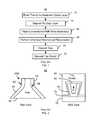
- FIG. 1is a flow chart depicting a conventional method 10 for fabricating a conventional perpendicular magnetic recording (PMR) transducer. For simplicity, some steps are omitted.
- the conventional method 10is used for providing a PMR pole in an aluminum oxide layer.
- a trenchis formed in the aluminum oxide layer, via step 12 .
- the top of the trenchis wider than the trench bottom.
- the PMR pole formed thereinwill have its top surface wider than its bottom. Consequently, the sidewalls of the PMR pole will have a reverse angle.
- a Ru gap layeris deposited, via step 14 .
- the Ru gap layeris used in forming a side gap.
- Step 14typically includes depositing the Ru gap layer using chemical vapor deposition (CVD).
- CVDchemical vapor deposition
- the conventional PMR pole materialsare plated, via step 16 .
- Step 16may include plating ferromagnetic pole materials as well as seed and/or other layer(s).
- a chemical mechanical planarization (CMP)is then performed, via step 18 .
- the write gap and top shieldare then deposited, via steps 20 and 22 , respectively.
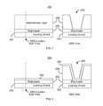
- FIG. 2depicts plan and air-bearing surface (ABS) views of a portion of a conventional PMR transducer 50 formed using the conventional method 10 .
- the conventional transducer 50includes an underlayer 52 , Ru gap layer 54 which is deposited in the trench (not shown).
- the pole 60 , write gap 70 and top shield 80are also shown.
- the pole 60may be formed.
- the conventional method 10may provide the conventional PMR transducer 50 , there may be drawbacks.
- the performance of the conventional PMR transducer 50is desired to be improved.
- the magnetic track width variationis also desired to be reduced.
- the geometry of the conventional pole 60is desired to be well controlled during fabrication.
- the radius of curvature at the corner 66 near the nose lengthis desired to be small.
- the radius of curvature at the corner 64 of the Ru gap layer 54is small.
- the corner 66 of the pole 60is less sharp. Stated differently, the radius of curvature of the pole 60 is larger. Consequently, the magnetic track width variation may be larger than desired.
- the variation in the width of the side gap layers 54may be larger than desired. Performance and manufacturability of the conventional magnetic recording transducer 50 may thus be adversely affected. Accordingly, what is needed is an improved method for fabricating a PMR transducer.
- a method for fabricating a magnetic transducer having a nonmagnetic intermediate layerincludes providing a trench in the intermediate layer and providing a first nonmagnetic gap layer.
- the trenchhas a profile and a location corresponding to a pole of the magnetic transducer. At least a portion of the first nonmagnetic gap layer resides in the trench.
- the methodalso includes providing a pole including at least one magnetic material. At least a portion of the pole resides in the trench and on the portion of the nonmagnetic layer in the trench.
- the methodalso includes removing at least a portion of the intermediate layer adjacent to the pole and then providing a second nonmagnetic gap layer.
- the second nonmagnetic gap layeris thicker than the first nonmagnetic gap layer.
- a portion of the second nonmagnetic layer and a portion of the first nonmagnetic layer adjacent to the poleform a side gap.
- the methodalso includes providing a side shield and providing a gap. The gap is on the pole, the side gap, and a portion of the side shield.
- the methodalso provides a top shield.
- FIG. 1is a flow chart depicting a conventional method for fabricating a PMR transducer.
- FIG. 2is a diagram depicting plan and ABS views of a conventional PMR transducer.
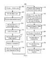
- FIG. 3is a flow chart depicting an exemplary embodiment of a method for fabricating a PMR transducer.
- FIG. 4is a diagram depicting an exemplary embodiment of a PMR transducer.
- FIG. 5is a diagram depicting an exemplary embodiment of a PMR head.
- FIG. 6is a flow chart depicting another exemplary embodiment of a method for fabricating a PMR transducer.
- FIGS. 7-17are diagrams depicting an exemplary embodiment of a magnetic recording transducer during fabrication.
- FIG. 3is a flow chart depicting an exemplary embodiment of a method 100 for fabricating a transducer.
- the method 100is described in the context of a PMR transducer, though other transducers might be so fabricated. For simplicity, some steps may be omitted and/or combined.
- the PMR transducer being fabricatedmay be part of a merged head that also includes a read head (not shown) and resides on a slider (not shown) in a disk drive.
- the method 100also may commence after formation of other portions of the PMR transducer.
- the method 100is also described in the context of providing a single PMR pole and its associated structures in a single magnetic recording transducer. However, the method 100 may be used to fabricate multiple transducers at substantially the same time.
- the method 100 and systemare also described in the context of particular layers. However, in some embodiments, such layers may include multiple sub-layers.
- the method 100commences after formation of the underlayer(s) on which the PMR pole is to reside as well as a nonmagnetic intermediate layer.
- the intermediate layeris an aluminum oxide layer.
- the underlayermay include an etch stop layer.
- a leading edge shieldis desired. In such embodiments, the leading edge shield may be provided under the underlayer.
- the leading edge shieldis generally ferromagnetic, magnetically soft, and may include materials such as NiFe.
- a trenchis formed in a portion of the intermediate, via step 102 .
- Trench formationmay include a reactive ion etch (RIE).
- RIEreactive ion etch
- the RIEmay terminate in the stop layer.
- the trench bottommay be formed by a portion of the stop layer.
- the trenchmay terminate in other layers including but not limited to the intermediate layer and an underlying shield layer.
- the RIE used in step 102may be an aluminum oxide RIE.
- the trenchhas a profile and a location that correspond to the pole being formed. Thus, the trench may have a top wider than its bottom and is located where the pole is to be formed.
- a first nonmagnetic gap layeris provided, via step 104 . At least a portion of the first nonmagnetic gap layer resides in the trench formed in step 102 . Thus, step 104 may include blanket depositing the nonmagnetic gap layer over a region that extends across the trench.
- the first nonmagnetic gap layermay be a Ru layer.
- step 104includes performing chemical vapor deposition (CVD) of the layer of Ru.
- the first nonmagnetic gap layerhas a thickness that is less than the total desired thickness of the side gap. In some embodiments, the first nonmagnetic gap layer is at least five and not more than thirty-five nanometers thick. In some such embodiments, the first nonmagnetic gap layer is at least fifteen and not more than twenty-five nanometers thick.
- Step 106may include providing one or more seed layers, and then depositing the magnetic layer(s) for the pole. For example sputtering and/or plating may be used for the magnetic layers.
- the magnetic layer(s) depositedare desired to be high moment layers, which may be plated. At least part of the magnetic layer(s) resides in the trench as well as on the part of the first nonmagnetic layer in the trench.
- step 106may include planarizing the magnetic transducer. Thus, an exposed portion of the first nonmagnetic gap layer external to the trench and an exposed portion of the at least one magnetic layer external to the trench may be removed. The pole may then include the remaining magnetic material in the trench.
- Step 108A portion of the intermediate layer adjacent to the pole is removed, via step 108 .
- all of the intermediate layer in the device regionis removed.
- Step 108may include wet etching the intermediate layer, for example using an aluminum oxide wet etch.
- a second nonmagnetic gap layeris provided after the portion of the intermediate layer adjacent to the pole is removed, via step 110 .
- the second nonmagnetic gap layermay include multiple sublayers.
- the second nonmagnetic gap layermay include a layer of aluminum oxide and a Ru layer.
- the Ru layeris formed via CVD, while the aluminum oxide layer may be formed using atomic layer deposition (ALD).
- the second nonmagnetic gap layermay be a single layer, such as a layer of Ru.
- the second nonmagnetic gap layer provided in step 110thicker than the first nonmagnetic gap layer deposited in step 104 .
- the second nonmagnetic gap layermay be at least twenty and not more than one hundred nanometers thick.
- the second nonmagnetic gap layeris at least twenty-five and not more than thirty-five nanometers thick. If the second nonmagnetic gap includes only a Ru layer, then the Ru layer may have the above thicknesses. If a bilayer is used, then the insulating layer (e.g. aluminum oxide layer) may be at least fifteen and not more than sixty nanometers thick and the additional Ru layer may be at least five and not more than thirty five nanometers thick. In some such embodiments, the Ru layer is at least fifteen and not more than twenty-five nanometers thick. However, the total thickness of the second nonmagnetic layer is greater than the thickness of the first nonmagnetic layer.
- the insulating layere.g. aluminum oxide layer
- the first nonmagnetic gap layer and the second nonmagnetic gap layer togetherhave a total thickness of at least thirty nanometers and not more than one hundred nanometers. In some embodiments, the total thickness of the first and second nonmagnetic gap layers together is at least thirty and not more than ninety nanometers. A portion of the second nonmagnetic layer and a portion of the first nonmagnetic layer adjacent to the pole form a side gap for the transducer being fabricated.
- Step 112may include depositing a high permeability layer, such as NiFe, and planarizing the transducer. Thus, portion of the second gap layer on the pole may be exposed. In addition, the pole may be exposed either through the CMP or through an additional removal step, such as an ion mill.
- a high permeability layersuch as NiFe
- a write gapis provided, via step 114 .
- Step 114thus includes depositing a nonmagnetic layer. At least a portion of the write gap resides on the pole and on the side gap. In some embodiments, part of the write gap extends to cover at least part of the side shield. Step 114 may thus include blanket depositing a nonmagnetic gap layer and removing a portion of the gap layer distal from the pole.
- a top shieldis provided, via step 116 .
- FIG. 4is a diagram depicting an exemplary embodiment of a portion of a PMR transducer 150 that may be formed using the method 100 .
- FIG. 5depicts a head 180 incorporating the transducer 200 .
- FIGS. 4-5are not to scale.
- FIG. 4depicts plan and ABS views of the transducer 200
- FIG. 5depicts a side view only of the head 180 .
- the head 180 shownincludes a read transducer 182 and the PMR transducer 150 ′.
- the transducer 150 / 150 ′may be used in a head including only one or more write transducers 150 / 150 ′.
- the read transducer 182includes shields 184 and 188 as well as sensor 186 .
- the PMR transducer 150 ′ shown in FIG. 5includes shield 190 , pole 194 and coils 192 in addition to the PMR transducer 150 ′.
- the PMR transducer 150 / 150 ′includes underlay 152 / 152 ′, first and second nonmagnetic layer(s) 154 / 154 ′ and 170 , pole 160 / 160 ′, write gap 174 / 174 ′, side shields 172 , write gap 174 / 174 ′, and trailing shield 176 / 176 ′.
- Other and/or different componentsmay be fabricated in other embodiments. For example, a leading shield (not shown) may be included.
- a stop layermay also reside between the leading shield and the bottom of the pole 160 / 160 ′.
- the pole 160is shown as includes an optional leading edge bevel 162 and an optional trailing bevel 164 . However, in some embodiments, the bevels 162 and/or 164 may be omitted. Also shown is the ABS. As shown in the plan view, the pole 160 has corner 166 , while the nonmagnetic layers 154 / 170 has corners 155 .
- pole 160 / 160 ′ having the desired geometrymay be fabricated. More specifically, the corners 166 of the pole 160 / 160 ′ may be sharper, having a smaller radius of curvature.
- the thicknesses of the layers 154 and 170are well controlled. Thus, the side gap 154 / 170 thickness may be better controlled. As a result, the variation in the magnetic track width may be reduced. Consequently, manufacturing and performance of the transducer 150 / 150 ′ and head 180 may be improved. Further, the write gap 174 / 174 ′ and side gaps 154 / 170 may be separately optimized. Performance of the magnetic transducer 150 / 150 ′ and head 180 may thus be enhanced.
- the side shields 172 and trailing shield 176 / 176 ′may be coupled. Thus, the control of the side shield 172 may also be enhanced.
- FIG. 6is a flow chart depicting another exemplary embodiment of a method 200 for fabricating a PMR transducer. For simplicity, some steps may be omitted.
- FIGS. 7-17are diagrams depicting side and ABS views of an exemplary embodiment of a portion of a PMR transducer during 250 fabrication. For clarity, FIGS. 7-17 are not to scale. The side views in FIGS. 7-17 are taken in the middle of the location at which the pole is formed. Further, although FIGS. 7-17 depict the ABS location (location at which the ABS is to be formed) and ABS at a particular point in the pole, other embodiments may have other locations for the ABS. Referring to FIGS. 6-17 , the method 200 is described in the context of the PMR transducer 250 .
- the method 200may be used to form another device (not shown).
- the PMR transducer 250 being fabricatedmay be part of a merged head that also includes a read head (not shown in FIGS. 7-17 ) and resides on a slider (not shown) in a disk drive.
- the method 200also may commence after formation of other portions of the PMR transducer 250 .
- the method 200is also described in the context of providing a single PMR transducer 250 .
- the method 200may be used to fabricate multiple transducers at substantially the same time.
- the method 200 and device 250are also described in the context of particular layers. However, in some embodiments, such layers may include multiple sublayers.
- a leading shield layeris deposited, via step 202 .
- a NiFe layermay be deposited.
- the leading shield layeris deposited on a flat surface, for example a surface that has undergone a CMP.
- a planarization layeris deposited on the leading shield, via step 204 .
- step 204may include depositing a multilayer.
- An intermediate layeris deposited, via step 206 .
- the intermediate layermay be aluminum oxide.
- the stop layer provided in step 204is a stop layer for a removal process used to remove portions of the intermediate layer.
- Step 208includes providing a mask having an aperture therein.
- the maskincludes a hard mask having one or more layers.
- the aperturecorresponds to the location and footprint of the trench.
- the trenchmay be formed, for example by an alumina RIE.
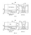
- FIG. 7depicts the transducer 250 after step 208 has been performed. Thus, a leading shield 252 and stop layer 254 are shown. In other embodiments, the leading shield 252 may be omitted.
- intermediate layer 256having trench 258 therein. In the side view, the intermediate layer 256 is shown by a dashed line as the portion of the intermediate layer 256 in the center of the trench 258 has been removed.
- the top surface of the stop layer 254forms the bottom of the trench 258 .
- the bottom of the trench 258may be within the intermediate layer 256 , within the stop layer 254 , within the leading shield 252 or at another location.
- the trench 258has a profile and location corresponding to the pole to be formed. Thus, the top of the trench 258 is wider than the bottom.
- the bottom of the trench 258might be configured to form a leading edge bevel in the pole being fabricated.
- step 210includes depositing a first Ru layer via CVD.
- FIG. 8depicts the transducer 250 after step 210 is performed.
- layer 260is shown.
- the layer 260is at least five and not more than thirty-five nanometers thick.
- the first Ru layer 260is at least fifteen and not more than twenty-five nanometers thick.
- Step 212thus includes providing one or more layers.
- CoNiFemay be plated in step 212 .
- different deposition techniques and/or materialsmay be used.
- magnetic and/or nonmagnetic seed layersmay also be deposited.
- the full filmis plated in step 212 .
- a framemay be provided and portions of the full film etched in step 212 .
- FIG. 9depicts the transducer after the pole material(s) have been deposited.
- magnetic materials 262are shown.
- the transduceris planarized, via step 214 .
- the planarization performed in step 214may include a CMP.
- step 214also includes ion beam etching the transducer.
- FIG. 10depicts the transducer 250 after step 214 is completed.
- the portions of the pole materials 262have been removed, leaving pole 262 ′.
- the top of the pole 262 ′is thus substantially coplanar with the tops of the intermediate layer 256 ′.
- Portions of the first nonmagnetic layer 260have also been removed, leaving first nonmagnetic layer 260 ′ adjoining the pole 262 ′.
- the transduceris wet etched to remove the intermediate layer adjacent to the pole 262 ′, via step 216 .
- one or more solvents appropriate for the intermediate layer 256 ′are used in step 164 .
- FIG. 11depicts the transducer 250 after step 216 is completed.
- the intermediate layer 256 ′has been removed.
- An aluminum oxide layeris deposited using ALD, via step 218 .
- An additional Ru layeris then deposited, via step 220 .
- the additional Ru layermay be deposited using CVD.
- the aluminum oxide layeris at least fifteen and not more than sixty nanometers thick.
- the additional Ru layermay be at least five and not more than thirty-five nanometers thick.
- the additional Ru layeris at least fifteen and not more than twenty-five nanometers thick.
- the total combined thickness of the aluminum oxide and Ru layersis desired to be at least thirty nanometers and not more than one hundred nanometers.
- the total combined thickness of the aluminum oxide and Ru layersis also desired to be greater than the thickness of the first Ru layer deposited in step 210 .
- the aluminum oxide layer 264 and the Ru layer 266are shown. Note that although the aluminum oxide layer 264 and Ru layer 266 are shown as having substantially the same thickness in FIG. 12 , the relationship between the thicknesses of the layers 264 and 266 may differ. Further, although shown as approximately twice as thick as the first Ru layer 260 ′, the total combined thickness of the layers 264 and 266 may have another value as long as the combined thickness is greater than the thickness of the first Ru layer 260 ′.
- a magnetic side shieldis also plated, via step 222 .
- NiFemay be plated.
- seed layer(s)may be deposited.
- FIG. 13depicts the transducer 250 after step 222 is completed.
- magnetic side shield layer(s) 268are shown.
- the side shield layer(s) 268adjoin the nonmagnetic layer 266 .
- the transduceris planarized, via step 224 .
- FIG. 14depicts the transducer 250 after step 224 .
- a CMPmay be performed.
- the pole 262 ′may be exposed using an ion beam etch, via step 226 .
- Steps 222 - 226may thus be considered to form the side shields.
- FIG. 15depicts the transducer 250 after step 226 is performed.
- side shields 268 ′′have been formed.
- the top of the pole 262 ′′has been exposed.
- Nonmagnetic layers 260 ′′, 264 ′′, and 266 ′′also remain at the sides of the pole.
- a portion of the nonmagnetic layer 260 ′is also below the pole, while portions of the layers 266 ′′ and 268 ′′ are below the side shields 268 ′′.
- a write gapmay be provided, via step 228 .
- step 228may include providing a layer of alumina using atomic layer deposition and removing a portion of the gap layer distal from the pole 262 ′′.
- FIG. 16depicts the transducer 250 after step 228 is performed. Thus, a gap layer 270 is shown.
- a trailing edge, or top, shieldmay then be provided, via step 230 .
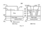
- FIG. 17depicts the transducer 250 after step 230 .
- top shield material 272is shown.
- the shield materials 272may include CoNiFe.
- the PMR transducer 250may be fabricated.
- the PMR transducer 250has the desired geometry.
- the corners of the pole 262 ′may have a smaller radius of curvature and the thickness of the side gap 260 ′/ 264 ′/ 266 ′ may be better controlled.
- the write gap 270 and side gap 260 ′/ 264 ′/ 266 ′can be independently controlled and optimized. Consequently, manufacturing and performance of the transducer 250 may be improved.
Landscapes
- Engineering & Computer Science (AREA)
- Manufacturing & Machinery (AREA)
- Physics & Mathematics (AREA)
- Electromagnetism (AREA)
- Magnetic Heads (AREA)
Abstract
Description
Claims (21)
Priority Applications (1)
| Application Number | Priority Date | Filing Date | Title |
|---|---|---|---|
| US12/886,999US8444866B1 (en) | 2010-09-21 | 2010-09-21 | Method and system for providing a perpendicular magnetic recording pole with a multi-layer side gap |
Applications Claiming Priority (1)
| Application Number | Priority Date | Filing Date | Title |
|---|---|---|---|
| US12/886,999US8444866B1 (en) | 2010-09-21 | 2010-09-21 | Method and system for providing a perpendicular magnetic recording pole with a multi-layer side gap |
Publications (1)
| Publication Number | Publication Date |
|---|---|
| US8444866B1true US8444866B1 (en) | 2013-05-21 |
Family
ID=48365295
Family Applications (1)
| Application Number | Title | Priority Date | Filing Date |
|---|---|---|---|
| US12/886,999Expired - Fee RelatedUS8444866B1 (en) | 2010-09-21 | 2010-09-21 | Method and system for providing a perpendicular magnetic recording pole with a multi-layer side gap |
Country Status (1)
| Country | Link |
|---|---|
| US (1) | US8444866B1 (en) |
Cited By (134)
| Publication number | Priority date | Publication date | Assignee | Title |
|---|---|---|---|---|
| US8628672B1 (en)* | 2012-06-27 | 2014-01-14 | Western Digital (Fremont), Llc | Process for manufacturing a perpendicular magnetic recording writer pole with nonmagnetic bevel |
| US8797686B1 (en) | 2010-12-23 | 2014-08-05 | Western Digital (Fremont), Llc | Magnetic recording transducer with short effective throat height and method of fabrication |
| US8830628B1 (en) | 2009-02-23 | 2014-09-09 | Western Digital (Fremont), Llc | Method and system for providing a perpendicular magnetic recording head |
| US8879207B1 (en) | 2011-12-20 | 2014-11-04 | Western Digital (Fremont), Llc | Method for providing a side shield for a magnetic recording transducer using an air bridge |
| US8883017B1 (en) | 2013-03-12 | 2014-11-11 | Western Digital (Fremont), Llc | Method and system for providing a read transducer having seamless interfaces |
| US8917581B1 (en) | 2013-12-18 | 2014-12-23 | Western Digital Technologies, Inc. | Self-anneal process for a near field transducer and chimney in a hard disk drive assembly |
| US8923102B1 (en) | 2013-07-16 | 2014-12-30 | Western Digital (Fremont), Llc | Optical grating coupling for interferometric waveguides in heat assisted magnetic recording heads |
| US8947985B1 (en) | 2013-07-16 | 2015-02-03 | Western Digital (Fremont), Llc | Heat assisted magnetic recording transducers having a recessed pole |
| US8953422B1 (en) | 2014-06-10 | 2015-02-10 | Western Digital (Fremont), Llc | Near field transducer using dielectric waveguide core with fine ridge feature |
| US8958272B1 (en) | 2014-06-10 | 2015-02-17 | Western Digital (Fremont), Llc | Interfering near field transducer for energy assisted magnetic recording |
| US8970988B1 (en) | 2013-12-31 | 2015-03-03 | Western Digital (Fremont), Llc | Electric gaps and method for making electric gaps for multiple sensor arrays |
| US8971160B1 (en) | 2013-12-19 | 2015-03-03 | Western Digital (Fremont), Llc | Near field transducer with high refractive index pin for heat assisted magnetic recording |
| US8976635B1 (en) | 2014-06-10 | 2015-03-10 | Western Digital (Fremont), Llc | Near field transducer driven by a transverse electric waveguide for energy assisted magnetic recording |
| US8982508B1 (en) | 2011-10-31 | 2015-03-17 | Western Digital (Fremont), Llc | Method for providing a side shield for a magnetic recording transducer |
| US8980109B1 (en) | 2012-12-11 | 2015-03-17 | Western Digital (Fremont), Llc | Method for providing a magnetic recording transducer using a combined main pole and side shield CMP for a wraparound shield scheme |
| US8988812B1 (en) | 2013-11-27 | 2015-03-24 | Western Digital (Fremont), Llc | Multi-sensor array configuration for a two-dimensional magnetic recording (TDMR) operation |
| US8984740B1 (en) | 2012-11-30 | 2015-03-24 | Western Digital (Fremont), Llc | Process for providing a magnetic recording transducer having a smooth magnetic seed layer |
| US8988825B1 (en) | 2014-02-28 | 2015-03-24 | Western Digital (Fremont, LLC | Method for fabricating a magnetic writer having half-side shields |
| US8993217B1 (en) | 2013-04-04 | 2015-03-31 | Western Digital (Fremont), Llc | Double exposure technique for high resolution disk imaging |
| US8995087B1 (en) | 2006-11-29 | 2015-03-31 | Western Digital (Fremont), Llc | Perpendicular magnetic recording write head having a wrap around shield |
| US8997832B1 (en) | 2010-11-23 | 2015-04-07 | Western Digital (Fremont), Llc | Method of fabricating micrometer scale components |
| US9001467B1 (en) | 2014-03-05 | 2015-04-07 | Western Digital (Fremont), Llc | Method for fabricating side shields in a magnetic writer |
| US9001628B1 (en) | 2013-12-16 | 2015-04-07 | Western Digital (Fremont), Llc | Assistant waveguides for evaluating main waveguide coupling efficiency and diode laser alignment tolerances for hard disk |
| US9007719B1 (en) | 2013-10-23 | 2015-04-14 | Western Digital (Fremont), Llc | Systems and methods for using double mask techniques to achieve very small features |
| US9007879B1 (en) | 2014-06-10 | 2015-04-14 | Western Digital (Fremont), Llc | Interfering near field transducer having a wide metal bar feature for energy assisted magnetic recording |
| US9007725B1 (en) | 2014-10-07 | 2015-04-14 | Western Digital (Fremont), Llc | Sensor with positive coupling between dual ferromagnetic free layer laminates |
| US9013836B1 (en) | 2013-04-02 | 2015-04-21 | Western Digital (Fremont), Llc | Method and system for providing an antiferromagnetically coupled return pole |
| US9042058B1 (en) | 2013-10-17 | 2015-05-26 | Western Digital Technologies, Inc. | Shield designed for middle shields in a multiple sensor array |
| US9042051B2 (en) | 2013-08-15 | 2015-05-26 | Western Digital (Fremont), Llc | Gradient write gap for perpendicular magnetic recording writer |
| US9042052B1 (en) | 2014-06-23 | 2015-05-26 | Western Digital (Fremont), Llc | Magnetic writer having a partially shunted coil |
| US9042057B1 (en) | 2013-01-09 | 2015-05-26 | Western Digital (Fremont), Llc | Methods for providing magnetic storage elements with high magneto-resistance using Heusler alloys |
| US9042208B1 (en) | 2013-03-11 | 2015-05-26 | Western Digital Technologies, Inc. | Disk drive measuring fly height by applying a bias voltage to an electrically insulated write component of a head |
| US9053735B1 (en) | 2014-06-20 | 2015-06-09 | Western Digital (Fremont), Llc | Method for fabricating a magnetic writer using a full-film metal planarization |
| US9064507B1 (en) | 2009-07-31 | 2015-06-23 | Western Digital (Fremont), Llc | Magnetic etch-stop layer for magnetoresistive read heads |
| US9065043B1 (en) | 2012-06-29 | 2015-06-23 | Western Digital (Fremont), Llc | Tunnel magnetoresistance read head with narrow shield-to-shield spacing |
| US9064527B1 (en) | 2013-04-12 | 2015-06-23 | Western Digital (Fremont), Llc | High order tapered waveguide for use in a heat assisted magnetic recording head |
| US9064528B1 (en) | 2013-05-17 | 2015-06-23 | Western Digital Technologies, Inc. | Interferometric waveguide usable in shingled heat assisted magnetic recording in the absence of a near-field transducer |
| US9070381B1 (en) | 2013-04-12 | 2015-06-30 | Western Digital (Fremont), Llc | Magnetic recording read transducer having a laminated free layer |
| US9082423B1 (en) | 2013-12-18 | 2015-07-14 | Western Digital (Fremont), Llc | Magnetic recording write transducer having an improved trailing surface profile |
| US20150199982A1 (en)* | 2014-01-13 | 2015-07-16 | Seagate Technology Llc | Varying Write Pole Side Shield Gap |
| US9087534B1 (en) | 2011-12-20 | 2015-07-21 | Western Digital (Fremont), Llc | Method and system for providing a read transducer having soft and hard magnetic bias structures |
| US9087527B1 (en) | 2014-10-28 | 2015-07-21 | Western Digital (Fremont), Llc | Apparatus and method for middle shield connection in magnetic recording transducers |
| US9093639B2 (en) | 2012-02-21 | 2015-07-28 | Western Digital (Fremont), Llc | Methods for manufacturing a magnetoresistive structure utilizing heating and cooling |
| US9104107B1 (en) | 2013-04-03 | 2015-08-11 | Western Digital (Fremont), Llc | DUV photoresist process |
| US9111558B1 (en) | 2014-03-14 | 2015-08-18 | Western Digital (Fremont), Llc | System and method of diffractive focusing of light in a waveguide |
| US9111550B1 (en) | 2014-12-04 | 2015-08-18 | Western Digital (Fremont), Llc | Write transducer having a magnetic buffer layer spaced between a side shield and a write pole by non-magnetic layers |
| US9111564B1 (en) | 2013-04-02 | 2015-08-18 | Western Digital (Fremont), Llc | Magnetic recording writer having a main pole with multiple flare angles |
| US9123362B1 (en) | 2011-03-22 | 2015-09-01 | Western Digital (Fremont), Llc | Methods for assembling an electrically assisted magnetic recording (EAMR) head |
| US9123374B1 (en) | 2015-02-12 | 2015-09-01 | Western Digital (Fremont), Llc | Heat assisted magnetic recording writer having an integrated polarization rotation plate |
| US9123358B1 (en) | 2012-06-11 | 2015-09-01 | Western Digital (Fremont), Llc | Conformal high moment side shield seed layer for perpendicular magnetic recording writer |
| US9123359B1 (en) | 2010-12-22 | 2015-09-01 | Western Digital (Fremont), Llc | Magnetic recording transducer with sputtered antiferromagnetic coupling trilayer between plated ferromagnetic shields and method of fabrication |
| US9135937B1 (en) | 2014-05-09 | 2015-09-15 | Western Digital (Fremont), Llc | Current modulation on laser diode for energy assisted magnetic recording transducer |
| US9135930B1 (en) | 2014-03-06 | 2015-09-15 | Western Digital (Fremont), Llc | Method for fabricating a magnetic write pole using vacuum deposition |
| US9142233B1 (en) | 2014-02-28 | 2015-09-22 | Western Digital (Fremont), Llc | Heat assisted magnetic recording writer having a recessed pole |
| US9147404B1 (en) | 2015-03-31 | 2015-09-29 | Western Digital (Fremont), Llc | Method and system for providing a read transducer having a dual free layer |
| US9147408B1 (en) | 2013-12-19 | 2015-09-29 | Western Digital (Fremont), Llc | Heated AFM layer deposition and cooling process for TMR magnetic recording sensor with high pinning field |
| US9153255B1 (en) | 2014-03-05 | 2015-10-06 | Western Digital (Fremont), Llc | Method for fabricating a magnetic writer having an asymmetric gap and shields |
| US9183854B2 (en) | 2014-02-24 | 2015-11-10 | Western Digital (Fremont), Llc | Method to make interferometric taper waveguide for HAMR light delivery |
| US9190079B1 (en) | 2014-09-22 | 2015-11-17 | Western Digital (Fremont), Llc | Magnetic write pole having engineered radius of curvature and chisel angle profiles |
| US9190085B1 (en) | 2014-03-12 | 2015-11-17 | Western Digital (Fremont), Llc | Waveguide with reflective grating for localized energy intensity |
| US9194692B1 (en) | 2013-12-06 | 2015-11-24 | Western Digital (Fremont), Llc | Systems and methods for using white light interferometry to measure undercut of a bi-layer structure |
| US9202480B2 (en) | 2009-10-14 | 2015-12-01 | Western Digital (Fremont), LLC. | Double patterning hard mask for damascene perpendicular magnetic recording (PMR) writer |
| US9202493B1 (en) | 2014-02-28 | 2015-12-01 | Western Digital (Fremont), Llc | Method of making an ultra-sharp tip mode converter for a HAMR head |
| US9214172B2 (en) | 2013-10-23 | 2015-12-15 | Western Digital (Fremont), Llc | Method of manufacturing a magnetic read head |
| US9213322B1 (en) | 2012-08-16 | 2015-12-15 | Western Digital (Fremont), Llc | Methods for providing run to run process control using a dynamic tuner |
| US9214165B1 (en) | 2014-12-18 | 2015-12-15 | Western Digital (Fremont), Llc | Magnetic writer having a gradient in saturation magnetization of the shields |
| US9214169B1 (en) | 2014-06-20 | 2015-12-15 | Western Digital (Fremont), Llc | Magnetic recording read transducer having a laminated free layer |
| US9230565B1 (en) | 2014-06-24 | 2016-01-05 | Western Digital (Fremont), Llc | Magnetic shield for magnetic recording head |
| US9236560B1 (en) | 2014-12-08 | 2016-01-12 | Western Digital (Fremont), Llc | Spin transfer torque tunneling magnetoresistive device having a laminated free layer with perpendicular magnetic anisotropy |
| US9245562B1 (en) | 2015-03-30 | 2016-01-26 | Western Digital (Fremont), Llc | Magnetic recording writer with a composite main pole |
| US9245545B1 (en) | 2013-04-12 | 2016-01-26 | Wester Digital (Fremont), Llc | Short yoke length coils for magnetic heads in disk drives |
| US9245543B1 (en) | 2010-06-25 | 2016-01-26 | Western Digital (Fremont), Llc | Method for providing an energy assisted magnetic recording head having a laser integrally mounted to the slider |
| US9251813B1 (en) | 2009-04-19 | 2016-02-02 | Western Digital (Fremont), Llc | Method of making a magnetic recording head |
| US9263071B1 (en) | 2015-03-31 | 2016-02-16 | Western Digital (Fremont), Llc | Flat NFT for heat assisted magnetic recording |
| US9263067B1 (en) | 2013-05-29 | 2016-02-16 | Western Digital (Fremont), Llc | Process for making PMR writer with constant side wall angle |
| US9269382B1 (en) | 2012-06-29 | 2016-02-23 | Western Digital (Fremont), Llc | Method and system for providing a read transducer having improved pinning of the pinned layer at higher recording densities |
| US9275657B1 (en) | 2013-08-14 | 2016-03-01 | Western Digital (Fremont), Llc | Process for making PMR writer with non-conformal side gaps |
| US9280990B1 (en) | 2013-12-11 | 2016-03-08 | Western Digital (Fremont), Llc | Method for fabricating a magnetic writer using multiple etches |
| US9286919B1 (en) | 2014-12-17 | 2016-03-15 | Western Digital (Fremont), Llc | Magnetic writer having a dual side gap |
| US9287494B1 (en) | 2013-06-28 | 2016-03-15 | Western Digital (Fremont), Llc | Magnetic tunnel junction (MTJ) with a magnesium oxide tunnel barrier |
| US9305583B1 (en) | 2014-02-18 | 2016-04-05 | Western Digital (Fremont), Llc | Method for fabricating a magnetic writer using multiple etches of damascene materials |
| US9312064B1 (en) | 2015-03-02 | 2016-04-12 | Western Digital (Fremont), Llc | Method to fabricate a magnetic head including ion milling of read gap using dual layer hard mask |
| US9318130B1 (en) | 2013-07-02 | 2016-04-19 | Western Digital (Fremont), Llc | Method to fabricate tunneling magnetic recording heads with extended pinned layer |
| US9336814B1 (en) | 2013-03-12 | 2016-05-10 | Western Digital (Fremont), Llc | Inverse tapered waveguide for use in a heat assisted magnetic recording head |
| US9343098B1 (en) | 2013-08-23 | 2016-05-17 | Western Digital (Fremont), Llc | Method for providing a heat assisted magnetic recording transducer having protective pads |
| US9343087B1 (en) | 2014-12-21 | 2016-05-17 | Western Digital (Fremont), Llc | Method for fabricating a magnetic writer having half shields |
| US9343086B1 (en) | 2013-09-11 | 2016-05-17 | Western Digital (Fremont), Llc | Magnetic recording write transducer having an improved sidewall angle profile |
| US9349392B1 (en) | 2012-05-24 | 2016-05-24 | Western Digital (Fremont), Llc | Methods for improving adhesion on dielectric substrates |
| US9349394B1 (en) | 2013-10-18 | 2016-05-24 | Western Digital (Fremont), Llc | Method for fabricating a magnetic writer having a gradient side gap |
| US9361914B1 (en) | 2014-06-18 | 2016-06-07 | Western Digital (Fremont), Llc | Magnetic sensor with thin capping layer |
| US9361913B1 (en) | 2013-06-03 | 2016-06-07 | Western Digital (Fremont), Llc | Recording read heads with a multi-layer AFM layer methods and apparatuses |
| US9368134B1 (en) | 2010-12-16 | 2016-06-14 | Western Digital (Fremont), Llc | Method and system for providing an antiferromagnetically coupled writer |
| US9384765B1 (en) | 2015-09-24 | 2016-07-05 | Western Digital (Fremont), Llc | Method and system for providing a HAMR writer having improved optical efficiency |
| US9384763B1 (en) | 2015-03-26 | 2016-07-05 | Western Digital (Fremont), Llc | Dual free layer magnetic reader having a rear bias structure including a soft bias layer |
| US9396743B1 (en) | 2014-02-28 | 2016-07-19 | Western Digital (Fremont), Llc | Systems and methods for controlling soft bias thickness for tunnel magnetoresistance readers |
| US9396742B1 (en) | 2012-11-30 | 2016-07-19 | Western Digital (Fremont), Llc | Magnetoresistive sensor for a magnetic storage system read head, and fabrication method thereof |
| US9406331B1 (en) | 2013-06-17 | 2016-08-02 | Western Digital (Fremont), Llc | Method for making ultra-narrow read sensor and read transducer device resulting therefrom |
| US9424866B1 (en) | 2015-09-24 | 2016-08-23 | Western Digital (Fremont), Llc | Heat assisted magnetic recording write apparatus having a dielectric gap |
| US9431047B1 (en) | 2013-05-01 | 2016-08-30 | Western Digital (Fremont), Llc | Method for providing an improved AFM reader shield |
| US9431031B1 (en) | 2015-03-24 | 2016-08-30 | Western Digital (Fremont), Llc | System and method for magnetic transducers having multiple sensors and AFC shields |
| US9431032B1 (en) | 2013-08-14 | 2016-08-30 | Western Digital (Fremont), Llc | Electrical connection arrangement for a multiple sensor array usable in two-dimensional magnetic recording |
| US9431038B1 (en) | 2015-06-29 | 2016-08-30 | Western Digital (Fremont), Llc | Method for fabricating a magnetic write pole having an improved sidewall angle profile |
| US9431039B1 (en) | 2013-05-21 | 2016-08-30 | Western Digital (Fremont), Llc | Multiple sensor array usable in two-dimensional magnetic recording |
| US9437251B1 (en) | 2014-12-22 | 2016-09-06 | Western Digital (Fremont), Llc | Apparatus and method having TDMR reader to reader shunts |
| US9441938B1 (en) | 2013-10-08 | 2016-09-13 | Western Digital (Fremont), Llc | Test structures for measuring near field transducer disc length |
| US9443541B1 (en) | 2015-03-24 | 2016-09-13 | Western Digital (Fremont), Llc | Magnetic writer having a gradient in saturation magnetization of the shields and return pole |
| US9449621B1 (en) | 2015-03-26 | 2016-09-20 | Western Digital (Fremont), Llc | Dual free layer magnetic reader having a rear bias structure having a high aspect ratio |
| US9449625B1 (en) | 2014-12-24 | 2016-09-20 | Western Digital (Fremont), Llc | Heat assisted magnetic recording head having a plurality of diffusion barrier layers |
| US9472216B1 (en) | 2015-09-23 | 2016-10-18 | Western Digital (Fremont), Llc | Differential dual free layer magnetic reader |
| US9484051B1 (en) | 2015-11-09 | 2016-11-01 | The Provost, Fellows, Foundation Scholars and the other members of Board, of the College of the Holy and Undivided Trinity of Queen Elizabeth near Dublin | Method and system for reducing undesirable reflections in a HAMR write apparatus |
| US9489969B1 (en)* | 2015-10-28 | 2016-11-08 | Headway Technologies, Inc. | Magnetic head including a main pole and a write shield to provide improved write characteristics without compromising the function of the write shield |
| US9508372B1 (en) | 2015-06-03 | 2016-11-29 | Western Digital (Fremont), Llc | Shingle magnetic writer having a low sidewall angle pole |
| US9508363B1 (en) | 2014-06-17 | 2016-11-29 | Western Digital (Fremont), Llc | Method for fabricating a magnetic write pole having a leading edge bevel |
| US9508365B1 (en) | 2015-06-24 | 2016-11-29 | Western Digital (Fremont), LLC. | Magnetic reader having a crystal decoupling structure |
| US9530443B1 (en) | 2015-06-25 | 2016-12-27 | Western Digital (Fremont), Llc | Method for fabricating a magnetic recording device having a high aspect ratio structure |
| US9564150B1 (en) | 2015-11-24 | 2017-02-07 | Western Digital (Fremont), Llc | Magnetic read apparatus having an improved read sensor isolation circuit |
| US9595273B1 (en) | 2015-09-30 | 2017-03-14 | Western Digital (Fremont), Llc | Shingle magnetic writer having nonconformal shields |
| US9646639B2 (en) | 2015-06-26 | 2017-05-09 | Western Digital (Fremont), Llc | Heat assisted magnetic recording writer having integrated polarization rotation waveguides |
| US9666214B1 (en) | 2015-09-23 | 2017-05-30 | Western Digital (Fremont), Llc | Free layer magnetic reader that may have a reduced shield-to-shield spacing |
| US9721595B1 (en) | 2014-12-04 | 2017-08-01 | Western Digital (Fremont), Llc | Method for providing a storage device |
| US9741366B1 (en) | 2014-12-18 | 2017-08-22 | Western Digital (Fremont), Llc | Method for fabricating a magnetic writer having a gradient in saturation magnetization of the shields |
| US9740805B1 (en) | 2015-12-01 | 2017-08-22 | Western Digital (Fremont), Llc | Method and system for detecting hotspots for photolithographically-defined devices |
| US9754611B1 (en) | 2015-11-30 | 2017-09-05 | Western Digital (Fremont), Llc | Magnetic recording write apparatus having a stepped conformal trailing shield |
| US9767831B1 (en) | 2015-12-01 | 2017-09-19 | Western Digital (Fremont), Llc | Magnetic writer having convex trailing surface pole and conformal write gap |
| US9786301B1 (en) | 2014-12-02 | 2017-10-10 | Western Digital (Fremont), Llc | Apparatuses and methods for providing thin shields in a multiple sensor array |
| US9799351B1 (en) | 2015-11-30 | 2017-10-24 | Western Digital (Fremont), Llc | Short yoke length writer having assist coils |
| US9812155B1 (en) | 2015-11-23 | 2017-11-07 | Western Digital (Fremont), Llc | Method and system for fabricating high junction angle read sensors |
| US9842615B1 (en) | 2015-06-26 | 2017-12-12 | Western Digital (Fremont), Llc | Magnetic reader having a nonmagnetic insertion layer for the pinning layer |
| US9858951B1 (en) | 2015-12-01 | 2018-01-02 | Western Digital (Fremont), Llc | Method for providing a multilayer AFM layer in a read sensor |
| US9881638B1 (en) | 2014-12-17 | 2018-01-30 | Western Digital (Fremont), Llc | Method for providing a near-field transducer (NFT) for a heat assisted magnetic recording (HAMR) device |
| US9934811B1 (en) | 2014-03-07 | 2018-04-03 | Western Digital (Fremont), Llc | Methods for controlling stray fields of magnetic features using magneto-elastic anisotropy |
| US9953670B1 (en) | 2015-11-10 | 2018-04-24 | Western Digital (Fremont), Llc | Method and system for providing a HAMR writer including a multi-mode interference device |
| US10037770B1 (en) | 2015-11-12 | 2018-07-31 | Western Digital (Fremont), Llc | Method for providing a magnetic recording write apparatus having a seamless pole |
| US10074387B1 (en) | 2014-12-21 | 2018-09-11 | Western Digital (Fremont), Llc | Method and system for providing a read transducer having symmetric antiferromagnetically coupled shields |
Citations (39)
| Publication number | Priority date | Publication date | Assignee | Title |
|---|---|---|---|---|
| US5540346A (en) | 1994-07-01 | 1996-07-30 | Intel Corporation | Method of making integrated circuit waveguide |
| US20050237665A1 (en) | 2004-04-21 | 2005-10-27 | Dialog Semiconductor Gmbh | Four sided shield structure for a perpendicular write head |
| US20060044682A1 (en) | 2004-08-31 | 2006-03-02 | Quang Le | Self aligned wrap around shield for perpendicular magnetic recording |
| US20060044681A1 (en) | 2004-08-31 | 2006-03-02 | Quang Le | Write pole and method of manufacturing the same |
| US20060225268A1 (en) | 2005-03-29 | 2006-10-12 | Hitachi Global Storage Technologies Netherlands B.V. | Manufacturable CMP assisted liftoff process to fabricate write pole for perpendicular recording heads |
| US20060288565A1 (en) | 2003-09-26 | 2006-12-28 | Hitachi Global Storage Technologies | Write pole fabrication for perpendicular recording |
| US7159302B2 (en) | 2004-03-31 | 2007-01-09 | Hitachi Global Storage Technologies Netherlands B.V. | Method for manufacturing a perpendicular write head |
| US20070115584A1 (en) | 2005-11-23 | 2007-05-24 | Hitachi Global Storage Technologies | Write head design and method for reducing adjacent track interference in at very narrow track widths |
| US20070177301A1 (en) | 2006-02-02 | 2007-08-02 | Headway Technologies, Inc. | Method to make a perpendicular magnetic recording head with a side write shield |
| US20080026254A1 (en) | 2004-02-23 | 2008-01-31 | Richard Hsiao | Perpendicular pole structure and method of fabricating the same |
| US20080100959A1 (en) | 2006-10-27 | 2008-05-01 | Hitachi Global Storage Technologies | Magnetic write head having a shield that extends below the leading edge of the write pole |
| US7367112B2 (en) | 2006-02-14 | 2008-05-06 | Hitachi Global Storage Technologies Netherlands B.V. | Method of fabricating a head for perpendicular magnetic recording with a self-aligning side shield structure |
| US20080110761A1 (en) | 2006-11-10 | 2008-05-15 | Hieu Lam | Metal capped seed layers for the fabrication of wrap around and trailing shields |
| US20080113090A1 (en) | 2006-11-10 | 2008-05-15 | Hieu Lam | Anti-reflective seed layers for the fabrication of wrap around and trailing shields |
| US20080151437A1 (en) | 2006-12-26 | 2008-06-26 | Tsung Yuan Chen | Perpendicular magnetic recording head including wrap around shield with notched top write gap and method of fabricating the same |
| US7430095B2 (en) | 2003-11-20 | 2008-09-30 | Maxtor Corporation | Tapered write pole for reduced skew effect |
| US20080253035A1 (en)* | 2007-03-27 | 2008-10-16 | Headway Technologies, Inc. | Self-aligned full side shield PMR and method to make it |
| US7444740B1 (en) | 2005-01-31 | 2008-11-04 | Western Digital (Fremont), Llc | Damascene process for fabricating poles in recording heads |
| US20080273276A1 (en) | 2007-04-13 | 2008-11-06 | Headway Technologies, Inc. | Optimized write pole flare angle for side shield or semi side shield PMR writer application |
| US20080273277A1 (en) | 2007-04-13 | 2008-11-06 | Headway Technologies, Inc | Composite shield structure of PMR writer for high track density |
| US20080278861A1 (en) | 2007-05-11 | 2008-11-13 | Ming Jiang | Stitched wrap around shield fabrication for perpendicular magnetic recording write heads |
| US20080297945A1 (en) | 2007-05-31 | 2008-12-04 | Headway Technologies, Inc. | Method to make a perpendicular magnetic recording head with a bottom side shield |
| US20090002885A1 (en) | 2007-06-28 | 2009-01-01 | Samsung Electronics Co., Ltd. | Perpendicular magnetic recording head and method of manufacturing the same |
| US7506431B2 (en) | 2007-05-03 | 2009-03-24 | Hitachi Global Storage Technologies Netherlands B.V. | Method of manufacturing a perpendicular magnetic write head having a wrap-around trailing shield and a concave trailing edge main pole |
| US20090116145A1 (en) | 2007-11-02 | 2009-05-07 | Headway Technologies, Inc. | Perpendicular shield pole writer with tapered main pole and tapered non-magnetic top shaping layer |
| US20090128952A1 (en) | 2007-11-15 | 2009-05-21 | Tdk Corporation | Magnetic head, head assembly and magnetic recording/reproducing apparatus |
| US7549213B2 (en) | 2005-01-12 | 2009-06-23 | Hitachi Global Storage Technologies Netherlands B.V. | Method for independent trackwidth and wall angle control and hexagonal write head |
| US20090168242A1 (en) | 2007-12-28 | 2009-07-02 | Yinshi Liu | Method for manufacturing a perpendicular magnetic write pole having a large bevel angle |
| US20090184091A1 (en) | 2008-01-22 | 2009-07-23 | Yi Zheng | Diamond-like carbon (dlc) hardmask and methods of fabrication using same |
| US20090195920A1 (en) | 2008-01-31 | 2009-08-06 | Bonhote Christian R | Main pole bridge structure |
| US7576951B2 (en) | 2006-04-25 | 2009-08-18 | Hitachi Global Storage Technologies Netherlands B.V. | Perpendicular magnetic write head having a magnetic write pole with a concave trailing edge |
| US20100062177A1 (en) | 2008-09-08 | 2010-03-11 | Ming Jiang | Method for manufacturing a perpendicular magnetic write head having a slanted write pole |
| US20100061016A1 (en)* | 2008-09-05 | 2010-03-11 | Headway Technologies, Inc. | Method to make an integrated side shield PMR head with non conformal side gap |
| US20100112486A1 (en) | 2008-10-31 | 2010-05-06 | Western Digital (Fremont), Llc | Method and system for providing a perpendicular magnetic recording head |
| US20110094888A1 (en)* | 2009-10-26 | 2011-04-28 | Headway Technologies, Inc. | Rejuvenation method for ruthenium plating seed |
| US8077434B1 (en) | 2007-11-19 | 2011-12-13 | Western Digital (Fremont), Llc | Perpendicular magnetic recording head having a recessed magnetic base layer |
| US8166631B1 (en)* | 2008-08-27 | 2012-05-01 | Western Digital (Fremont), Llc | Method for fabricating a magnetic recording transducer having side shields |
| US8277669B1 (en) | 2009-12-21 | 2012-10-02 | Western Digital (Fremont), Llc | Method and system for providing a perpendicular magnetic recording pole having a leading edge bevel |
| US8375564B1 (en) | 2009-12-08 | 2013-02-19 | Western Digital (Fremont), Llc | Method for fabricating a pole of a magnetic transducer |
- 2010
- 2010-09-21USUS12/886,999patent/US8444866B1/ennot_activeExpired - Fee Related
Patent Citations (42)
| Publication number | Priority date | Publication date | Assignee | Title |
|---|---|---|---|---|
| US5540346A (en) | 1994-07-01 | 1996-07-30 | Intel Corporation | Method of making integrated circuit waveguide |
| US20060288565A1 (en) | 2003-09-26 | 2006-12-28 | Hitachi Global Storage Technologies | Write pole fabrication for perpendicular recording |
| US7464457B2 (en) | 2003-09-26 | 2008-12-16 | Hitachi Global Storage Technologies Netherlands B.V. | Method for forming a write head having an air bearing surface (ABS) |
| US7430095B2 (en) | 2003-11-20 | 2008-09-30 | Maxtor Corporation | Tapered write pole for reduced skew effect |
| US20080026254A1 (en) | 2004-02-23 | 2008-01-31 | Richard Hsiao | Perpendicular pole structure and method of fabricating the same |
| US7159302B2 (en) | 2004-03-31 | 2007-01-09 | Hitachi Global Storage Technologies Netherlands B.V. | Method for manufacturing a perpendicular write head |
| US20050237665A1 (en) | 2004-04-21 | 2005-10-27 | Dialog Semiconductor Gmbh | Four sided shield structure for a perpendicular write head |
| US20060044681A1 (en) | 2004-08-31 | 2006-03-02 | Quang Le | Write pole and method of manufacturing the same |
| US20060044682A1 (en) | 2004-08-31 | 2006-03-02 | Quang Le | Self aligned wrap around shield for perpendicular magnetic recording |
| US7565732B2 (en) | 2004-08-31 | 2009-07-28 | Hitachi Global Storage Technologies Netherlands B.V. | Method of manufacturing a write pole |
| US7549213B2 (en) | 2005-01-12 | 2009-06-23 | Hitachi Global Storage Technologies Netherlands B.V. | Method for independent trackwidth and wall angle control and hexagonal write head |
| US7444740B1 (en) | 2005-01-31 | 2008-11-04 | Western Digital (Fremont), Llc | Damascene process for fabricating poles in recording heads |
| US20060225268A1 (en) | 2005-03-29 | 2006-10-12 | Hitachi Global Storage Technologies Netherlands B.V. | Manufacturable CMP assisted liftoff process to fabricate write pole for perpendicular recording heads |
| US20070115584A1 (en) | 2005-11-23 | 2007-05-24 | Hitachi Global Storage Technologies | Write head design and method for reducing adjacent track interference in at very narrow track widths |
| US20070177301A1 (en) | 2006-02-02 | 2007-08-02 | Headway Technologies, Inc. | Method to make a perpendicular magnetic recording head with a side write shield |
| US7367112B2 (en) | 2006-02-14 | 2008-05-06 | Hitachi Global Storage Technologies Netherlands B.V. | Method of fabricating a head for perpendicular magnetic recording with a self-aligning side shield structure |
| US7576951B2 (en) | 2006-04-25 | 2009-08-18 | Hitachi Global Storage Technologies Netherlands B.V. | Perpendicular magnetic write head having a magnetic write pole with a concave trailing edge |
| US20080100959A1 (en) | 2006-10-27 | 2008-05-01 | Hitachi Global Storage Technologies | Magnetic write head having a shield that extends below the leading edge of the write pole |
| US20080110761A1 (en) | 2006-11-10 | 2008-05-15 | Hieu Lam | Metal capped seed layers for the fabrication of wrap around and trailing shields |
| US20080113090A1 (en) | 2006-11-10 | 2008-05-15 | Hieu Lam | Anti-reflective seed layers for the fabrication of wrap around and trailing shields |
| US20080151437A1 (en) | 2006-12-26 | 2008-06-26 | Tsung Yuan Chen | Perpendicular magnetic recording head including wrap around shield with notched top write gap and method of fabricating the same |
| US7979978B2 (en) | 2007-03-27 | 2011-07-19 | Headway Technologies, Inc. | Method for manufacturing a self-aligned full side shield PMR |
| US20080253035A1 (en)* | 2007-03-27 | 2008-10-16 | Headway Technologies, Inc. | Self-aligned full side shield PMR and method to make it |
| US20080273277A1 (en) | 2007-04-13 | 2008-11-06 | Headway Technologies, Inc | Composite shield structure of PMR writer for high track density |
| US20080273276A1 (en) | 2007-04-13 | 2008-11-06 | Headway Technologies, Inc. | Optimized write pole flare angle for side shield or semi side shield PMR writer application |
| US7506431B2 (en) | 2007-05-03 | 2009-03-24 | Hitachi Global Storage Technologies Netherlands B.V. | Method of manufacturing a perpendicular magnetic write head having a wrap-around trailing shield and a concave trailing edge main pole |
| US20080278861A1 (en) | 2007-05-11 | 2008-11-13 | Ming Jiang | Stitched wrap around shield fabrication for perpendicular magnetic recording write heads |
| US20080297945A1 (en) | 2007-05-31 | 2008-12-04 | Headway Technologies, Inc. | Method to make a perpendicular magnetic recording head with a bottom side shield |
| US20090002885A1 (en) | 2007-06-28 | 2009-01-01 | Samsung Electronics Co., Ltd. | Perpendicular magnetic recording head and method of manufacturing the same |
| US20090116145A1 (en) | 2007-11-02 | 2009-05-07 | Headway Technologies, Inc. | Perpendicular shield pole writer with tapered main pole and tapered non-magnetic top shaping layer |
| US20090128952A1 (en) | 2007-11-15 | 2009-05-21 | Tdk Corporation | Magnetic head, head assembly and magnetic recording/reproducing apparatus |
| US8077434B1 (en) | 2007-11-19 | 2011-12-13 | Western Digital (Fremont), Llc | Perpendicular magnetic recording head having a recessed magnetic base layer |
| US20090168242A1 (en) | 2007-12-28 | 2009-07-02 | Yinshi Liu | Method for manufacturing a perpendicular magnetic write pole having a large bevel angle |
| US20090184091A1 (en) | 2008-01-22 | 2009-07-23 | Yi Zheng | Diamond-like carbon (dlc) hardmask and methods of fabrication using same |
| US20090195920A1 (en) | 2008-01-31 | 2009-08-06 | Bonhote Christian R | Main pole bridge structure |
| US8166631B1 (en)* | 2008-08-27 | 2012-05-01 | Western Digital (Fremont), Llc | Method for fabricating a magnetic recording transducer having side shields |
| US20100061016A1 (en)* | 2008-09-05 | 2010-03-11 | Headway Technologies, Inc. | Method to make an integrated side shield PMR head with non conformal side gap |
| US20100062177A1 (en) | 2008-09-08 | 2010-03-11 | Ming Jiang | Method for manufacturing a perpendicular magnetic write head having a slanted write pole |
| US20100112486A1 (en) | 2008-10-31 | 2010-05-06 | Western Digital (Fremont), Llc | Method and system for providing a perpendicular magnetic recording head |
| US20110094888A1 (en)* | 2009-10-26 | 2011-04-28 | Headway Technologies, Inc. | Rejuvenation method for ruthenium plating seed |
| US8375564B1 (en) | 2009-12-08 | 2013-02-19 | Western Digital (Fremont), Llc | Method for fabricating a pole of a magnetic transducer |
| US8277669B1 (en) | 2009-12-21 | 2012-10-02 | Western Digital (Fremont), Llc | Method and system for providing a perpendicular magnetic recording pole having a leading edge bevel |
Cited By (153)
| Publication number | Priority date | Publication date | Assignee | Title |
|---|---|---|---|---|
| US8995087B1 (en) | 2006-11-29 | 2015-03-31 | Western Digital (Fremont), Llc | Perpendicular magnetic recording write head having a wrap around shield |
| US8830628B1 (en) | 2009-02-23 | 2014-09-09 | Western Digital (Fremont), Llc | Method and system for providing a perpendicular magnetic recording head |
| US9251813B1 (en) | 2009-04-19 | 2016-02-02 | Western Digital (Fremont), Llc | Method of making a magnetic recording head |
| US9064507B1 (en) | 2009-07-31 | 2015-06-23 | Western Digital (Fremont), Llc | Magnetic etch-stop layer for magnetoresistive read heads |
| US9202480B2 (en) | 2009-10-14 | 2015-12-01 | Western Digital (Fremont), LLC. | Double patterning hard mask for damascene perpendicular magnetic recording (PMR) writer |
| US9245543B1 (en) | 2010-06-25 | 2016-01-26 | Western Digital (Fremont), Llc | Method for providing an energy assisted magnetic recording head having a laser integrally mounted to the slider |
| US9159345B1 (en) | 2010-11-23 | 2015-10-13 | Western Digital (Fremont), Llc | Micrometer scale components |
| US9672847B2 (en) | 2010-11-23 | 2017-06-06 | Western Digital (Fremont), Llc | Micrometer scale components |
| US8997832B1 (en) | 2010-11-23 | 2015-04-07 | Western Digital (Fremont), Llc | Method of fabricating micrometer scale components |
| US9368134B1 (en) | 2010-12-16 | 2016-06-14 | Western Digital (Fremont), Llc | Method and system for providing an antiferromagnetically coupled writer |
| US9123359B1 (en) | 2010-12-22 | 2015-09-01 | Western Digital (Fremont), Llc | Magnetic recording transducer with sputtered antiferromagnetic coupling trilayer between plated ferromagnetic shields and method of fabrication |
| US8797686B1 (en) | 2010-12-23 | 2014-08-05 | Western Digital (Fremont), Llc | Magnetic recording transducer with short effective throat height and method of fabrication |
| US9123362B1 (en) | 2011-03-22 | 2015-09-01 | Western Digital (Fremont), Llc | Methods for assembling an electrically assisted magnetic recording (EAMR) head |
| US8982508B1 (en) | 2011-10-31 | 2015-03-17 | Western Digital (Fremont), Llc | Method for providing a side shield for a magnetic recording transducer |
| US8879207B1 (en) | 2011-12-20 | 2014-11-04 | Western Digital (Fremont), Llc | Method for providing a side shield for a magnetic recording transducer using an air bridge |
| US9087534B1 (en) | 2011-12-20 | 2015-07-21 | Western Digital (Fremont), Llc | Method and system for providing a read transducer having soft and hard magnetic bias structures |
| US9093639B2 (en) | 2012-02-21 | 2015-07-28 | Western Digital (Fremont), Llc | Methods for manufacturing a magnetoresistive structure utilizing heating and cooling |
| US9940950B2 (en) | 2012-05-24 | 2018-04-10 | Western Digital (Fremont), Llc | Methods for improving adhesion on dielectric substrates |
| US9349392B1 (en) | 2012-05-24 | 2016-05-24 | Western Digital (Fremont), Llc | Methods for improving adhesion on dielectric substrates |
| US9123358B1 (en) | 2012-06-11 | 2015-09-01 | Western Digital (Fremont), Llc | Conformal high moment side shield seed layer for perpendicular magnetic recording writer |
| US8628672B1 (en)* | 2012-06-27 | 2014-01-14 | Western Digital (Fremont), Llc | Process for manufacturing a perpendicular magnetic recording writer pole with nonmagnetic bevel |
| US9412400B2 (en) | 2012-06-29 | 2016-08-09 | Western Digital (Fremont), Llc | Tunnel magnetoresistance read head with narrow shield-to-shield spacing |
| US9269382B1 (en) | 2012-06-29 | 2016-02-23 | Western Digital (Fremont), Llc | Method and system for providing a read transducer having improved pinning of the pinned layer at higher recording densities |
| US9065043B1 (en) | 2012-06-29 | 2015-06-23 | Western Digital (Fremont), Llc | Tunnel magnetoresistance read head with narrow shield-to-shield spacing |
| US9213322B1 (en) | 2012-08-16 | 2015-12-15 | Western Digital (Fremont), Llc | Methods for providing run to run process control using a dynamic tuner |
| US8984740B1 (en) | 2012-11-30 | 2015-03-24 | Western Digital (Fremont), Llc | Process for providing a magnetic recording transducer having a smooth magnetic seed layer |
| US9396742B1 (en) | 2012-11-30 | 2016-07-19 | Western Digital (Fremont), Llc | Magnetoresistive sensor for a magnetic storage system read head, and fabrication method thereof |
| US8980109B1 (en) | 2012-12-11 | 2015-03-17 | Western Digital (Fremont), Llc | Method for providing a magnetic recording transducer using a combined main pole and side shield CMP for a wraparound shield scheme |
| US9042057B1 (en) | 2013-01-09 | 2015-05-26 | Western Digital (Fremont), Llc | Methods for providing magnetic storage elements with high magneto-resistance using Heusler alloys |
| US9042208B1 (en) | 2013-03-11 | 2015-05-26 | Western Digital Technologies, Inc. | Disk drive measuring fly height by applying a bias voltage to an electrically insulated write component of a head |
| US9336814B1 (en) | 2013-03-12 | 2016-05-10 | Western Digital (Fremont), Llc | Inverse tapered waveguide for use in a heat assisted magnetic recording head |
| US8883017B1 (en) | 2013-03-12 | 2014-11-11 | Western Digital (Fremont), Llc | Method and system for providing a read transducer having seamless interfaces |
| US9013836B1 (en) | 2013-04-02 | 2015-04-21 | Western Digital (Fremont), Llc | Method and system for providing an antiferromagnetically coupled return pole |
| US9111564B1 (en) | 2013-04-02 | 2015-08-18 | Western Digital (Fremont), Llc | Magnetic recording writer having a main pole with multiple flare angles |
| US9104107B1 (en) | 2013-04-03 | 2015-08-11 | Western Digital (Fremont), Llc | DUV photoresist process |
| US8993217B1 (en) | 2013-04-04 | 2015-03-31 | Western Digital (Fremont), Llc | Double exposure technique for high resolution disk imaging |
| US9245545B1 (en) | 2013-04-12 | 2016-01-26 | Wester Digital (Fremont), Llc | Short yoke length coils for magnetic heads in disk drives |
| US9064527B1 (en) | 2013-04-12 | 2015-06-23 | Western Digital (Fremont), Llc | High order tapered waveguide for use in a heat assisted magnetic recording head |
| US9070381B1 (en) | 2013-04-12 | 2015-06-30 | Western Digital (Fremont), Llc | Magnetic recording read transducer having a laminated free layer |
| US9431047B1 (en) | 2013-05-01 | 2016-08-30 | Western Digital (Fremont), Llc | Method for providing an improved AFM reader shield |
| US9064528B1 (en) | 2013-05-17 | 2015-06-23 | Western Digital Technologies, Inc. | Interferometric waveguide usable in shingled heat assisted magnetic recording in the absence of a near-field transducer |
| US9431039B1 (en) | 2013-05-21 | 2016-08-30 | Western Digital (Fremont), Llc | Multiple sensor array usable in two-dimensional magnetic recording |
| US9263067B1 (en) | 2013-05-29 | 2016-02-16 | Western Digital (Fremont), Llc | Process for making PMR writer with constant side wall angle |
| US9361913B1 (en) | 2013-06-03 | 2016-06-07 | Western Digital (Fremont), Llc | Recording read heads with a multi-layer AFM layer methods and apparatuses |
| US9406331B1 (en) | 2013-06-17 | 2016-08-02 | Western Digital (Fremont), Llc | Method for making ultra-narrow read sensor and read transducer device resulting therefrom |
| US9287494B1 (en) | 2013-06-28 | 2016-03-15 | Western Digital (Fremont), Llc | Magnetic tunnel junction (MTJ) with a magnesium oxide tunnel barrier |
| US9318130B1 (en) | 2013-07-02 | 2016-04-19 | Western Digital (Fremont), Llc | Method to fabricate tunneling magnetic recording heads with extended pinned layer |
| US8923102B1 (en) | 2013-07-16 | 2014-12-30 | Western Digital (Fremont), Llc | Optical grating coupling for interferometric waveguides in heat assisted magnetic recording heads |
| US8947985B1 (en) | 2013-07-16 | 2015-02-03 | Western Digital (Fremont), Llc | Heat assisted magnetic recording transducers having a recessed pole |
| US9431032B1 (en) | 2013-08-14 | 2016-08-30 | Western Digital (Fremont), Llc | Electrical connection arrangement for a multiple sensor array usable in two-dimensional magnetic recording |
| US9275657B1 (en) | 2013-08-14 | 2016-03-01 | Western Digital (Fremont), Llc | Process for making PMR writer with non-conformal side gaps |
| US9042051B2 (en) | 2013-08-15 | 2015-05-26 | Western Digital (Fremont), Llc | Gradient write gap for perpendicular magnetic recording writer |
| US9214166B1 (en) | 2013-08-15 | 2015-12-15 | Western Digital (Fremont), Llc | Gradient write gap for perpendicular magnetic recording writer |
| US9343098B1 (en) | 2013-08-23 | 2016-05-17 | Western Digital (Fremont), Llc | Method for providing a heat assisted magnetic recording transducer having protective pads |
| US9343086B1 (en) | 2013-09-11 | 2016-05-17 | Western Digital (Fremont), Llc | Magnetic recording write transducer having an improved sidewall angle profile |
| US9441938B1 (en) | 2013-10-08 | 2016-09-13 | Western Digital (Fremont), Llc | Test structures for measuring near field transducer disc length |
| US9042058B1 (en) | 2013-10-17 | 2015-05-26 | Western Digital Technologies, Inc. | Shield designed for middle shields in a multiple sensor array |
| US9349394B1 (en) | 2013-10-18 | 2016-05-24 | Western Digital (Fremont), Llc | Method for fabricating a magnetic writer having a gradient side gap |
| US9830936B2 (en) | 2013-10-23 | 2017-11-28 | Western Digital (Fremont), Llc | Magnetic read head with antiferromagentic layer |
| US9007719B1 (en) | 2013-10-23 | 2015-04-14 | Western Digital (Fremont), Llc | Systems and methods for using double mask techniques to achieve very small features |
| US9214172B2 (en) | 2013-10-23 | 2015-12-15 | Western Digital (Fremont), Llc | Method of manufacturing a magnetic read head |
| US8988812B1 (en) | 2013-11-27 | 2015-03-24 | Western Digital (Fremont), Llc | Multi-sensor array configuration for a two-dimensional magnetic recording (TDMR) operation |
| US9194692B1 (en) | 2013-12-06 | 2015-11-24 | Western Digital (Fremont), Llc | Systems and methods for using white light interferometry to measure undercut of a bi-layer structure |
| US9280990B1 (en) | 2013-12-11 | 2016-03-08 | Western Digital (Fremont), Llc | Method for fabricating a magnetic writer using multiple etches |
| US9001628B1 (en) | 2013-12-16 | 2015-04-07 | Western Digital (Fremont), Llc | Assistant waveguides for evaluating main waveguide coupling efficiency and diode laser alignment tolerances for hard disk |
| US9082423B1 (en) | 2013-12-18 | 2015-07-14 | Western Digital (Fremont), Llc | Magnetic recording write transducer having an improved trailing surface profile |
| US8917581B1 (en) | 2013-12-18 | 2014-12-23 | Western Digital Technologies, Inc. | Self-anneal process for a near field transducer and chimney in a hard disk drive assembly |
| US9147408B1 (en) | 2013-12-19 | 2015-09-29 | Western Digital (Fremont), Llc | Heated AFM layer deposition and cooling process for TMR magnetic recording sensor with high pinning field |
| US8971160B1 (en) | 2013-12-19 | 2015-03-03 | Western Digital (Fremont), Llc | Near field transducer with high refractive index pin for heat assisted magnetic recording |
| US8970988B1 (en) | 2013-12-31 | 2015-03-03 | Western Digital (Fremont), Llc | Electric gaps and method for making electric gaps for multiple sensor arrays |
| US9721590B2 (en)* | 2014-01-13 | 2017-08-01 | Seagate Technology Llc | Varying write pole side shield gap |
| US20150199982A1 (en)* | 2014-01-13 | 2015-07-16 | Seagate Technology Llc | Varying Write Pole Side Shield Gap |
| US9305583B1 (en) | 2014-02-18 | 2016-04-05 | Western Digital (Fremont), Llc | Method for fabricating a magnetic writer using multiple etches of damascene materials |
| US9183854B2 (en) | 2014-02-24 | 2015-11-10 | Western Digital (Fremont), Llc | Method to make interferometric taper waveguide for HAMR light delivery |
| US9396743B1 (en) | 2014-02-28 | 2016-07-19 | Western Digital (Fremont), Llc | Systems and methods for controlling soft bias thickness for tunnel magnetoresistance readers |
| US8988825B1 (en) | 2014-02-28 | 2015-03-24 | Western Digital (Fremont, LLC | Method for fabricating a magnetic writer having half-side shields |
| US9142233B1 (en) | 2014-02-28 | 2015-09-22 | Western Digital (Fremont), Llc | Heat assisted magnetic recording writer having a recessed pole |
| US9202493B1 (en) | 2014-02-28 | 2015-12-01 | Western Digital (Fremont), Llc | Method of making an ultra-sharp tip mode converter for a HAMR head |
| US9349393B2 (en) | 2014-03-05 | 2016-05-24 | Western Digital (Fremont), Llc | Magnetic writer having an asymmetric gap and shields |
| US9153255B1 (en) | 2014-03-05 | 2015-10-06 | Western Digital (Fremont), Llc | Method for fabricating a magnetic writer having an asymmetric gap and shields |
| US9001467B1 (en) | 2014-03-05 | 2015-04-07 | Western Digital (Fremont), Llc | Method for fabricating side shields in a magnetic writer |
| US9135930B1 (en) | 2014-03-06 | 2015-09-15 | Western Digital (Fremont), Llc | Method for fabricating a magnetic write pole using vacuum deposition |
| US9934811B1 (en) | 2014-03-07 | 2018-04-03 | Western Digital (Fremont), Llc | Methods for controlling stray fields of magnetic features using magneto-elastic anisotropy |
| US9495984B2 (en) | 2014-03-12 | 2016-11-15 | Western Digital (Fremont), Llc | Waveguide with reflective grating for localized energy intensity |
| US9190085B1 (en) | 2014-03-12 | 2015-11-17 | Western Digital (Fremont), Llc | Waveguide with reflective grating for localized energy intensity |
| US9111558B1 (en) | 2014-03-14 | 2015-08-18 | Western Digital (Fremont), Llc | System and method of diffractive focusing of light in a waveguide |
| US9135937B1 (en) | 2014-05-09 | 2015-09-15 | Western Digital (Fremont), Llc | Current modulation on laser diode for energy assisted magnetic recording transducer |
| US9159346B1 (en) | 2014-06-10 | 2015-10-13 | Western Digital (Fremont), Llc | Near field transducer using dielectric waveguide core with fine ridge feature |
| US8958272B1 (en) | 2014-06-10 | 2015-02-17 | Western Digital (Fremont), Llc | Interfering near field transducer for energy assisted magnetic recording |
| US9311952B2 (en) | 2014-06-10 | 2016-04-12 | Western Digital (Fremont), Llc | Interfering near field transducer for energy assisted magnetic recording |
| US9007879B1 (en) | 2014-06-10 | 2015-04-14 | Western Digital (Fremont), Llc | Interfering near field transducer having a wide metal bar feature for energy assisted magnetic recording |
| US8976635B1 (en) | 2014-06-10 | 2015-03-10 | Western Digital (Fremont), Llc | Near field transducer driven by a transverse electric waveguide for energy assisted magnetic recording |
| US8953422B1 (en) | 2014-06-10 | 2015-02-10 | Western Digital (Fremont), Llc | Near field transducer using dielectric waveguide core with fine ridge feature |
| US9508363B1 (en) | 2014-06-17 | 2016-11-29 | Western Digital (Fremont), Llc | Method for fabricating a magnetic write pole having a leading edge bevel |
| US9361914B1 (en) | 2014-06-18 | 2016-06-07 | Western Digital (Fremont), Llc | Magnetic sensor with thin capping layer |
| US9053735B1 (en) | 2014-06-20 | 2015-06-09 | Western Digital (Fremont), Llc | Method for fabricating a magnetic writer using a full-film metal planarization |
| US9214169B1 (en) | 2014-06-20 | 2015-12-15 | Western Digital (Fremont), Llc | Magnetic recording read transducer having a laminated free layer |
| US9042052B1 (en) | 2014-06-23 | 2015-05-26 | Western Digital (Fremont), Llc | Magnetic writer having a partially shunted coil |
| US9230565B1 (en) | 2014-06-24 | 2016-01-05 | Western Digital (Fremont), Llc | Magnetic shield for magnetic recording head |
| US9190079B1 (en) | 2014-09-22 | 2015-11-17 | Western Digital (Fremont), Llc | Magnetic write pole having engineered radius of curvature and chisel angle profiles |
| US9007725B1 (en) | 2014-10-07 | 2015-04-14 | Western Digital (Fremont), Llc | Sensor with positive coupling between dual ferromagnetic free layer laminates |
| US9087527B1 (en) | 2014-10-28 | 2015-07-21 | Western Digital (Fremont), Llc | Apparatus and method for middle shield connection in magnetic recording transducers |
| US9786301B1 (en) | 2014-12-02 | 2017-10-10 | Western Digital (Fremont), Llc | Apparatuses and methods for providing thin shields in a multiple sensor array |
| US9721595B1 (en) | 2014-12-04 | 2017-08-01 | Western Digital (Fremont), Llc | Method for providing a storage device |
| US9111550B1 (en) | 2014-12-04 | 2015-08-18 | Western Digital (Fremont), Llc | Write transducer having a magnetic buffer layer spaced between a side shield and a write pole by non-magnetic layers |
| US9705072B2 (en) | 2014-12-08 | 2017-07-11 | Western Digital (Fremont), Llc | Spin transfer torque tunneling magnetoresistive device having a laminated free layer with perpendicular magnetic anisotropy |
| US9236560B1 (en) | 2014-12-08 | 2016-01-12 | Western Digital (Fremont), Llc | Spin transfer torque tunneling magnetoresistive device having a laminated free layer with perpendicular magnetic anisotropy |
| US10553241B2 (en) | 2014-12-17 | 2020-02-04 | Western Digital Technologies, Inc. | Near-field transducer (NFT) for a heat assisted magnetic recording (HAMR) device |
| US9881638B1 (en) | 2014-12-17 | 2018-01-30 | Western Digital (Fremont), Llc | Method for providing a near-field transducer (NFT) for a heat assisted magnetic recording (HAMR) device |
| US9286919B1 (en) | 2014-12-17 | 2016-03-15 | Western Digital (Fremont), Llc | Magnetic writer having a dual side gap |
| US9741366B1 (en) | 2014-12-18 | 2017-08-22 | Western Digital (Fremont), Llc | Method for fabricating a magnetic writer having a gradient in saturation magnetization of the shields |
| US9214165B1 (en) | 2014-12-18 | 2015-12-15 | Western Digital (Fremont), Llc | Magnetic writer having a gradient in saturation magnetization of the shields |
| US10074387B1 (en) | 2014-12-21 | 2018-09-11 | Western Digital (Fremont), Llc | Method and system for providing a read transducer having symmetric antiferromagnetically coupled shields |
| US9343087B1 (en) | 2014-12-21 | 2016-05-17 | Western Digital (Fremont), Llc | Method for fabricating a magnetic writer having half shields |
| US9437251B1 (en) | 2014-12-22 | 2016-09-06 | Western Digital (Fremont), Llc | Apparatus and method having TDMR reader to reader shunts |
| US9449625B1 (en) | 2014-12-24 | 2016-09-20 | Western Digital (Fremont), Llc | Heat assisted magnetic recording head having a plurality of diffusion barrier layers |
| US9123374B1 (en) | 2015-02-12 | 2015-09-01 | Western Digital (Fremont), Llc | Heat assisted magnetic recording writer having an integrated polarization rotation plate |
| US9312064B1 (en) | 2015-03-02 | 2016-04-12 | Western Digital (Fremont), Llc | Method to fabricate a magnetic head including ion milling of read gap using dual layer hard mask |
| US9443541B1 (en) | 2015-03-24 | 2016-09-13 | Western Digital (Fremont), Llc | Magnetic writer having a gradient in saturation magnetization of the shields and return pole |
| US9754613B2 (en) | 2015-03-24 | 2017-09-05 | Western Digital (Fremont), Llc | Method for AFC shields for multiple sensor magnetic transducers and magnetic transducers having multiple sensors and AFC shields |
| US9431031B1 (en) | 2015-03-24 | 2016-08-30 | Western Digital (Fremont), Llc | System and method for magnetic transducers having multiple sensors and AFC shields |
| US9449621B1 (en) | 2015-03-26 | 2016-09-20 | Western Digital (Fremont), Llc | Dual free layer magnetic reader having a rear bias structure having a high aspect ratio |
| US9384763B1 (en) | 2015-03-26 | 2016-07-05 | Western Digital (Fremont), Llc | Dual free layer magnetic reader having a rear bias structure including a soft bias layer |
| US9922672B1 (en) | 2015-03-26 | 2018-03-20 | Western Digital (Fremont), Llc | Dual free layer magnetic reader having a rear bias structure having a high aspect ratio |
| US9245562B1 (en) | 2015-03-30 | 2016-01-26 | Western Digital (Fremont), Llc | Magnetic recording writer with a composite main pole |
| US9147404B1 (en) | 2015-03-31 | 2015-09-29 | Western Digital (Fremont), Llc | Method and system for providing a read transducer having a dual free layer |
| US9263071B1 (en) | 2015-03-31 | 2016-02-16 | Western Digital (Fremont), Llc | Flat NFT for heat assisted magnetic recording |
| US9508372B1 (en) | 2015-06-03 | 2016-11-29 | Western Digital (Fremont), Llc | Shingle magnetic writer having a low sidewall angle pole |
| US9508365B1 (en) | 2015-06-24 | 2016-11-29 | Western Digital (Fremont), LLC. | Magnetic reader having a crystal decoupling structure |
| US9530443B1 (en) | 2015-06-25 | 2016-12-27 | Western Digital (Fremont), Llc | Method for fabricating a magnetic recording device having a high aspect ratio structure |
| US10242700B2 (en) | 2015-06-26 | 2019-03-26 | Western Digital (Fremont), Llc | Magnetic reader having a nonmagnetic insertion layer for the pinning layer |
| US9646639B2 (en) | 2015-06-26 | 2017-05-09 | Western Digital (Fremont), Llc | Heat assisted magnetic recording writer having integrated polarization rotation waveguides |
| US9842615B1 (en) | 2015-06-26 | 2017-12-12 | Western Digital (Fremont), Llc | Magnetic reader having a nonmagnetic insertion layer for the pinning layer |
| US9431038B1 (en) | 2015-06-29 | 2016-08-30 | Western Digital (Fremont), Llc | Method for fabricating a magnetic write pole having an improved sidewall angle profile |
| US9472216B1 (en) | 2015-09-23 | 2016-10-18 | Western Digital (Fremont), Llc | Differential dual free layer magnetic reader |
| US9666214B1 (en) | 2015-09-23 | 2017-05-30 | Western Digital (Fremont), Llc | Free layer magnetic reader that may have a reduced shield-to-shield spacing |
| US9384765B1 (en) | 2015-09-24 | 2016-07-05 | Western Digital (Fremont), Llc | Method and system for providing a HAMR writer having improved optical efficiency |
| US9424866B1 (en) | 2015-09-24 | 2016-08-23 | Western Digital (Fremont), Llc | Heat assisted magnetic recording write apparatus having a dielectric gap |
| US9595273B1 (en) | 2015-09-30 | 2017-03-14 | Western Digital (Fremont), Llc | Shingle magnetic writer having nonconformal shields |
| US9489969B1 (en)* | 2015-10-28 | 2016-11-08 | Headway Technologies, Inc. | Magnetic head including a main pole and a write shield to provide improved write characteristics without compromising the function of the write shield |
| US9484051B1 (en) | 2015-11-09 | 2016-11-01 | The Provost, Fellows, Foundation Scholars and the other members of Board, of the College of the Holy and Undivided Trinity of Queen Elizabeth near Dublin | Method and system for reducing undesirable reflections in a HAMR write apparatus |
| US9953670B1 (en) | 2015-11-10 | 2018-04-24 | Western Digital (Fremont), Llc | Method and system for providing a HAMR writer including a multi-mode interference device |
| US10381029B2 (en) | 2015-11-10 | 2019-08-13 | Western Digital (Fremont), Llc | Method and system for providing a HAMR writer including a multi-mode interference device |
| US10037770B1 (en) | 2015-11-12 | 2018-07-31 | Western Digital (Fremont), Llc | Method for providing a magnetic recording write apparatus having a seamless pole |
| US9812155B1 (en) | 2015-11-23 | 2017-11-07 | Western Digital (Fremont), Llc | Method and system for fabricating high junction angle read sensors |
| US9564150B1 (en) | 2015-11-24 | 2017-02-07 | Western Digital (Fremont), Llc | Magnetic read apparatus having an improved read sensor isolation circuit |
| US10121495B2 (en) | 2015-11-30 | 2018-11-06 | Western Digital (Fremont), Llc | Magnetic recording write apparatus having a stepped conformal trailing shield |
| US9799351B1 (en) | 2015-11-30 | 2017-10-24 | Western Digital (Fremont), Llc | Short yoke length writer having assist coils |
| US9754611B1 (en) | 2015-11-30 | 2017-09-05 | Western Digital (Fremont), Llc | Magnetic recording write apparatus having a stepped conformal trailing shield |
| US9767831B1 (en) | 2015-12-01 | 2017-09-19 | Western Digital (Fremont), Llc | Magnetic writer having convex trailing surface pole and conformal write gap |
| US9740805B1 (en) | 2015-12-01 | 2017-08-22 | Western Digital (Fremont), Llc | Method and system for detecting hotspots for photolithographically-defined devices |
| US9997177B2 (en) | 2015-12-01 | 2018-06-12 | Western Digital (Fremont), Llc | Magnetic writer having convex trailing surface pole and conformal write gap |
| US9858951B1 (en) | 2015-12-01 | 2018-01-02 | Western Digital (Fremont), Llc | Method for providing a multilayer AFM layer in a read sensor |
Similar Documents
| Publication | Publication Date | Title |
|---|---|---|
| US8444866B1 (en) | Method and system for providing a perpendicular magnetic recording pole with a multi-layer side gap | |
| US8375564B1 (en) | Method for fabricating a pole of a magnetic transducer | |
| US8262919B1 (en) | Method and system for providing a perpendicular magnetic recording pole using multiple chemical mechanical planarizations | |
| US8879207B1 (en) | Method for providing a side shield for a magnetic recording transducer using an air bridge | |
| US8277669B1 (en) | Method and system for providing a perpendicular magnetic recording pole having a leading edge bevel | |
| US8320076B1 (en) | Method and system for providing a magnetic recording transducer including an assist pole having surfaces angled with respect to the ABS | |
| US8760807B1 (en) | Method for providing a wraparound shield for a magnetic recording transducer using a damascene process | |
| US8334093B2 (en) | Method and system for providing a perpendicular magnetic recording head | |
| US8705205B1 (en) | Magnetic recording head having a dual sidewall angle | |
| US8196285B1 (en) | Method and system for providing a pole for a perpendicular magnetic recording head using a multi-layer hard mask | |
| US8563146B1 (en) | Method and system for providing a magnetic recording pole having a dual sidewall angle | |
| US8231796B1 (en) | Method and system for providing a magnetic recording transducer having side shields | |
| US8409453B1 (en) | Method and system for providing a wrap-around shield using a patterned seed layer | |
| US8454846B1 (en) | Method and system for providing a full wrap-around shield using a frame configured wet etch in a damascene process | |
| US8079135B1 (en) | Method for providing a perpendicular magnetic recording (PMR) transducer | |
| US8419954B1 (en) | Method for providing a side shield for a magnetic recording transducer | |
| US8861134B1 (en) | Method and system for providing perpendicular magnetic recording transducers utilizing a damascene approach | |
| US8780498B1 (en) | System for providing a perpendicular magnetic recording transducer using a split seed layer | |
| US8720044B1 (en) | Method for manufacturing a magnetic recording transducer having side shields | |
| US8238059B1 (en) | PMR write head with narrow gap for minimal internal flux loss | |
| US8830628B1 (en) | Method and system for providing a perpendicular magnetic recording head | |
| US8276258B1 (en) | Method for fabricating a magnetic recording transducer | |
| US20140175050A1 (en) | Method for providing a magnetic recording transducer including a wraparound shield and a rectangular pole | |
| US20120237878A1 (en) | Method and system for providing a side shield for a perpendicular magnetic recording pole | |
| US9305583B1 (en) | Method for fabricating a magnetic writer using multiple etches of damascene materials |
Legal Events
| Date | Code | Title | Description |
|---|---|---|---|
| AS | Assignment | Owner name:WESTERN DIGITAL (FREMONT), LLC, CALIFORNIA Free format text:ASSIGNMENT OF ASSIGNORS INTEREST;ASSIGNORS:GUAN, LIJIE;SHI, CHANGQING;JIANG, MING;AND OTHERS;SIGNING DATES FROM 20100923 TO 20101206;REEL/FRAME:025457/0577 | |
| STCF | Information on status: patent grant | Free format text:PATENTED CASE | |
| AS | Assignment | Owner name:JPMORGAN CHASE BANK, N.A., AS COLLATERAL AGENT, IL Free format text:SECURITY AGREEMENT;ASSIGNOR:WESTERN DIGITAL (FREMONT), LLC;REEL/FRAME:038710/0845 Effective date:20160512 Owner name:U.S. BANK NATIONAL ASSOCIATION, AS COLLATERAL AGEN Free format text:SECURITY AGREEMENT;ASSIGNOR:WESTERN DIGITAL (FREMONT), LLC;REEL/FRAME:038744/0675 Effective date:20160512 Owner name:JPMORGAN CHASE BANK, N.A., AS COLLATERAL AGENT, IL Free format text:SECURITY AGREEMENT;ASSIGNOR:WESTERN DIGITAL (FREMONT), LLC;REEL/FRAME:038744/0755 Effective date:20160512 | |
| FPAY | Fee payment | Year of fee payment:4 | |
| AS | Assignment | Owner name:WESTERN DIGITAL (FREMONT), LLC, CALIFORNIA Free format text:RELEASE BY SECURED PARTY;ASSIGNOR:U.S. BANK NATIONAL ASSOCIATION, AS COLLATERAL AGENT;REEL/FRAME:045501/0158 Effective date:20180227 | |
| AS | Assignment | Owner name:WESTERN DIGITAL TECHNOLOGIES, INC., CALIFORNIA Free format text:ASSIGNMENT OF ASSIGNORS INTEREST;ASSIGNOR:WESTERN DIGITAL (FREMONT), LLC;REEL/FRAME:050450/0582 Effective date:20190508 | |
| MAFP | Maintenance fee payment | Free format text:PAYMENT OF MAINTENANCE FEE, 8TH YEAR, LARGE ENTITY (ORIGINAL EVENT CODE: M1552); ENTITY STATUS OF PATENT OWNER: LARGE ENTITY Year of fee payment:8 | |
| AS | Assignment | Owner name:WESTERN DIGITAL TECHNOLOGIES, INC., CALIFORNIA Free format text:RELEASE OF SECURITY INTEREST AT REEL 038710 FRAME 0845;ASSIGNOR:JPMORGAN CHASE BANK, N.A.;REEL/FRAME:058965/0445 Effective date:20220203 Owner name:WESTERN DIGITAL (FREMONT), LLC, CALIFORNIA Free format text:RELEASE OF SECURITY INTEREST AT REEL 038710 FRAME 0845;ASSIGNOR:JPMORGAN CHASE BANK, N.A.;REEL/FRAME:058965/0445 Effective date:20220203 | |
| AS | Assignment | Owner name:JPMORGAN CHASE BANK, N.A., ILLINOIS Free format text:PATENT COLLATERAL AGREEMENT - A&R LOAN AGREEMENT;ASSIGNOR:WESTERN DIGITAL TECHNOLOGIES, INC.;REEL/FRAME:064715/0001 Effective date:20230818 Owner name:JPMORGAN CHASE BANK, N.A., ILLINOIS Free format text:PATENT COLLATERAL AGREEMENT - DDTL LOAN AGREEMENT;ASSIGNOR:WESTERN DIGITAL TECHNOLOGIES, INC.;REEL/FRAME:067045/0156 Effective date:20230818 | |
| FEPP | Fee payment procedure | Free format text:MAINTENANCE FEE REMINDER MAILED (ORIGINAL EVENT CODE: REM.); ENTITY STATUS OF PATENT OWNER: LARGE ENTITY | |
| LAPS | Lapse for failure to pay maintenance fees | Free format text:PATENT EXPIRED FOR FAILURE TO PAY MAINTENANCE FEES (ORIGINAL EVENT CODE: EXP.); ENTITY STATUS OF PATENT OWNER: LARGE ENTITY | |
| STCH | Information on status: patent discontinuation | Free format text:PATENT EXPIRED DUE TO NONPAYMENT OF MAINTENANCE FEES UNDER 37 CFR 1.362 | |
| FP | Lapsed due to failure to pay maintenance fee | Effective date:20250521 |