US8441888B2 - Write command and write data timing circuit and methods for timing the same - Google Patents
Write command and write data timing circuit and methods for timing the sameDownload PDFInfo
- Publication number
- US8441888B2 US8441888B2US13/149,435US201113149435AUS8441888B2US 8441888 B2US8441888 B2US 8441888B2US 201113149435 AUS201113149435 AUS 201113149435AUS 8441888 B2US8441888 B2US 8441888B2
- Authority
- US
- United States
- Prior art keywords
- circuit
- signal
- command
- write
- clock
- Prior art date
- Legal status (The legal status is an assumption and is not a legal conclusion. Google has not performed a legal analysis and makes no representation as to the accuracy of the status listed.)
- Active, expires
Links
- 238000000034methodMethods0.000titleclaimsabstractdescription14
- 230000015654memoryEffects0.000claimsabstractdescription71
- 230000004044responseEffects0.000claimsabstractdescription61
- 230000000644propagated effectEffects0.000claimsabstractdescription4
- 230000001902propagating effectEffects0.000claimsdescription5
- 230000001934delayEffects0.000claimsdescription4
- 239000000872bufferSubstances0.000description43
- 230000000630rising effectEffects0.000description12
- 230000007704transitionEffects0.000description7
- 238000010586diagramMethods0.000description6
- 230000003111delayed effectEffects0.000description4
- 230000000295complement effectEffects0.000description3
- 230000001360synchronised effectEffects0.000description3
- 230000008859changeEffects0.000description2
- 238000012986modificationMethods0.000description2
- 230000004048modificationEffects0.000description2
- 239000004065semiconductorSubstances0.000description2
- 238000007796conventional methodMethods0.000description1
- 230000008569processEffects0.000description1
Images


Classifications
- G—PHYSICS
- G11—INFORMATION STORAGE
- G11C—STATIC STORES
- G11C7/00—Arrangements for writing information into, or reading information out from, a digital store
- G11C7/10—Input/output [I/O] data interface arrangements, e.g. I/O data control circuits, I/O data buffers
- G—PHYSICS
- G11—INFORMATION STORAGE
- G11C—STATIC STORES
- G11C7/00—Arrangements for writing information into, or reading information out from, a digital store
- G11C7/10—Input/output [I/O] data interface arrangements, e.g. I/O data control circuits, I/O data buffers
- G11C7/1078—Data input circuits, e.g. write amplifiers, data input buffers, data input registers, data input level conversion circuits
- G11C7/109—Control signal input circuits
- G—PHYSICS
- G11—INFORMATION STORAGE
- G11C—STATIC STORES
- G11C7/00—Arrangements for writing information into, or reading information out from, a digital store
- G11C7/22—Read-write [R-W] timing or clocking circuits; Read-write [R-W] control signal generators or management
- G—PHYSICS
- G11—INFORMATION STORAGE
- G11C—STATIC STORES
- G11C7/00—Arrangements for writing information into, or reading information out from, a digital store
- G11C7/22—Read-write [R-W] timing or clocking circuits; Read-write [R-W] control signal generators or management
- G11C7/222—Clock generating, synchronizing or distributing circuits within memory device
- G—PHYSICS
- G11—INFORMATION STORAGE
- G11C—STATIC STORES
- G11C8/00—Arrangements for selecting an address in a digital store
- G11C8/18—Address timing or clocking circuits; Address control signal generation or management, e.g. for row address strobe [RAS] or column address strobe [CAS] signals
- G—PHYSICS
- G11—INFORMATION STORAGE
- G11C—STATIC STORES
- G11C2207/00—Indexing scheme relating to arrangements for writing information into, or reading information out from, a digital store
- G11C2207/22—Control and timing of internal memory operations
- G11C2207/2272—Latency related aspects
Definitions
- Embodiments of the inventionrelate generally to semiconductor memory, and more specifically, to timing internal clock and control signals for executing memory commands in a high-speed memory clock system.
- write latencyis the delay, in clock cycles, from the issuance of a write command to the latching of the first write data.
- An example of typical write latencyis 12 clock cycles of the Clk signal.
- Correct timing of internal timing signals generated in response to external command and clock signalsis critical for proper operation of the memory. Complicating the generating of correctly timed internal signals is the relatively high frequency of memory clock signals. For example, memory clock signals can exceed 1 GHz. Further complicating the matter is that multi-data rate memories can provide and receive data at a rate higher than the memory clock signal. With respect to write commands, a write clock signal may be provided to the memory for correctly timing the rate at which write data is received by the memory. Correctly timing internal write operations relative to the receipt of the write command, write data, memory clock signal and write clock signal is required to properly complete a write operation.
- the traditional method of timing the write data with the memory clockis modeling both the write clock path and the system clock path to have the same propagation delay.
- the propagation delay of the clock pathsmay be on the order of several clock cycles, thus, preventing write throughput from being optimized. Additionally, the propagation delay can often vary due to power, voltage, and temperature conditions.
- tight phase control between the memory clock and the write clockis necessary for correct operation, which is complicated by the total propagation delay time and the variation in the delay due to power, voltage, and temperature conditions.
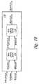
- FIG. 1Ais a block diagram of a write command-data timing circuit according to an embodiment of the invention.
- FIG. 1Bis a block diagram of a write latency multiplexer of FIG. 1A according to an embodiment of the invention.
- FIG. 2is a block diagram of a data input circuit according to an embodiment of the invention.
- FIG. 3is a timing diagram of various signals during operation of the write command-data timing circuit and the data input circuit according to an embodiment of the invention.
- FIG. 4is a block diagram of a memory device including a write command-data timing circuit according to an embodiment of the invention.
- FIG. 1Aillustrates a write command-data timing circuit 100 according to an embodiment of the invention.
- the timing circuit 100includes a memory clock and command buffer and clock circuit 110 .
- the buffer and clock circuit 110includes a command buffer 112 that buffers memory command signals Cmd and provides the buffered command signals CmdIBOut to a command latch 114 that captures the CmdIBOut signals.
- the captured CmdIBOutis provided to a command decoder 116 that decodes the CmdIBOut and generates internal device signals to carry out the decoded command.
- the command decoder 116generates internal write command signals WriteCmdY.
- the buffer and clock circuit 110further includes a memory clock buffer 122 that buffers the memory clock signal Clk and provides complementary buffered memory clock signals ClkIBOut, ClkIBOutF to a command latch and buffer model delay circuit 124 .
- the model delay circuit 124models the propagation delay of the command latch and buffer 114 .
- the command latch and buffer model delay circuit 124outputs an internal clock signal Clk2Dec to a command decoder model delay circuit 126 , which models the propagation delay of the command decoder 116 .
- the Clk2Dec signalis propagated through the command decoder model delay circuit 126 and provided as a write latency multiplexer clock signal Clk2LatMux.
- the Clk2LatMux signalhas the same frequency Clk signal.
- the model delay circuits 124 , 126approximate the delay through the command latch and buffer 114 and the command decoder 116 so that the WritecmdY and Clk2LatMux signals are roughly synchronized.
- a multi-phase write clock generator model delay circuit 128 coupled to the memory clock buffer 122is also included in the buffer and clock circuit 110 .
- the model delay circuit 128provides a delayed clock signal ClkTrkWClk4Ph ⁇ 0> in response to receiving the ClkIBOut signal from the input buffer 122 .
- the model delay circuit 128models the propagation delay of a multi-phase clock generator for a write clock signal.
- the Clk and Cmd signals provided to the buffer and clock circuit 110are considered to be in a first clock domain. That is, the Clk signal has a first clock domain frequency and the Cmd signals are latched according to the first clock domain frequency.
- the timing circuit 100further includes a write clock buffer and clock circuit 130 .
- the buffer and clock circuit 130include a write clock buffer 132 that buffers a write clock WClk and generates complementary buffered write clock signals WClkIBOut, WClkIBOutF.
- the WClkIBOut, WClkIBOutF signalsare provided to a multi-phase clock generator 134 that generates clock signals having fixed phase relationships to one another.
- the multi-phase clock generator 134is a four-phase clock generator that generates quadrature clock signals WClk4Ph ⁇ 0:3> in response to the WClkIBOut, WClkIBOutF signals.
- the four-phase clock generator 134generates a 0 degree clock signal synchronized with the WC1 kBOut signal, and further generates a 90 degree clock signal having a 90 degree phase relative to the 0 degree clock signal, a 180 degree clock signal and a 270 degree clock signal.
- the clock frequencies of the multi-phase clock signalsare the same clock frequency of the WClk signal.
- the clock frequencies of the multi-phase clock signalscan be greater or lower than the clock frequency of the WClk signal.
- the clock frequency of the multi-phase clock signalsare the same clock frequency as the Clk signal.
- the WClk signal provided to the buffer and clock circuit 130is in a second clock domain.
- the second clock domainmay have the same clock frequency as clock signals in the first clock domain.
- the second clock domainmay have a different clock frequency than clock signals in the first clock domain.
- the WClk signalmay have a clock frequency that is a multiple of the frequency of the Clk signal, such as twice the frequency of the Clk signal.
- the timing circuit 100further includes a write enable timing circuit 150 .
- the timing circuit 150includes clocked counter circuits 152 , 154 .
- the counter circuit 152is clocked by the 0 degree clock signal WClk4Ph ⁇ 0> from the multi-phase clock generator 134 and the counter circuit 154 is clocked by the ClkTrkWClk4Ph ⁇ 0> signal from the buffer and clock circuit 110 .
- the counter circuits 152 , 154will count in synchronicity.
- the output signals EnWrLvl ⁇ 0:3> from the counter circuit 152 and EnWrLat ⁇ 0:3> from the counter circuit 154change values at a frequency that is four times the frequency of the Clk signal.
- a reset circuit 140 coupled to the counter circuits 152 , 154generates a reset signal RstGTree to reset the count of the counter circuits 152 , 154 so that the counts of the two counter circuits 152 , 154 correspond to one another in response to the respective clock signals.
- Each of the counter circuits 152 , 154change the value of a binary digit of the count in response to the respective clock signal. For example, assuming that four-bit counter circuits are used for the counter circuits 152 , 154 , in response to a rising edge of the WClk4Ph ⁇ 0> signal the counter circuit 152 generates an output signal EnWrLvl ⁇ 0:3> representing the binary number 1000. In response to a next rising edge of the WClk4Ph ⁇ 0> signal the counter circuit 152 generates an output signal EnWrLvl ⁇ 0:3> representing the binary number 0100. The next binary number generated by the counter circuit 152 is 0010 and the following binary number is 0001.
- the counter circuit 152In response to the fifth rising edge of the WClk4Ph ⁇ 0> signal the counter circuit 152 generates an output signal EnWrLvl ⁇ 0:3> representing the binary number 1000.
- the counter circuit 154operates similarly in response to the ClkTrkWClk4Ph ⁇ 0> signal and generates an output signal EnWrLat ⁇ 0:3> representing the binary number.
- the timing circuit 150further includes a write latency multiplexer 156 .
- the write latency multiplexer 156delays the propagating WriteCmdY signal to account for write latency and latches the WriteCmdY from the command decoder 116 in response to the EnWrLat ⁇ 0:3> signal at a “position” corresponding to the value of EnWrLat ⁇ 0:3>.
- the captured WriteCmdY signalis then released from the write latency multiplexer 156 as a write command enable signal WEn4 ⁇ 0:3> in response to a subsequent occurrence of the EnWrLat ⁇ 0:3> signal having the same value as its respective latched position.
- the WriteCmdY signalis latched into the 0010 position.
- the WriteCmdY signal at the 0010 positionis released as a Wen4 ⁇ 0:3> signal.
- the write latency multiplexer 156has four positions and is implemented using four latches, each latch clocked by one of the EnWrLat ⁇ 0:3> signals.
- FIG. 1Billustrates a write latency multiplexer 170 according to an embodiment of the invention.
- the write latency multiplexer 156( FIG. 1A ) may be implemented as the write latency multiplexer 170 .
- the write latency multiplexer 170includes a write latency shifter 174 and a write latency shifter 178 .
- the WriteCmdY signalis shifted through a write latency shifter 174 in response to the Clk2LatMux signal to provide appropriate delay due to write latency.
- write latencyis the delay, in clock cycles, from the issuance of a write command to the latching of the first write data. Examples of typical write latency are between 12 and 16 clock cycles of the Clk signal.
- the write latency shifter 174may provide between 8 and 12 clock cycles of delay. After being shifted through the write latency shifter 174 , the WriteCmdY signal is output to the write latency shifter 178 as the WriteCmdZ signal. The WriteCmdZ signal is captured by the write latency shifter 178 in response to the EnWrLat ⁇ 0:3> signals.
- the WriteCmdZ signalis released from the write latency shifter 178 as the WEn4 ⁇ 0:3> signal in response to the EnWrLat ⁇ 0:3> signal having a value corresponding to the position in which the WriteCmdZ signal was captured in the write latency shifter 178 .
- the resulting WEn4 ⁇ 0:3> signalhas a value indicative of the latched position of the write command.
- the WriteCmdY signalis provided to the write latency multiplexer 170 and is shifted through the write latency shifter 174 in response to the Clk2LatMux signal.
- the write latency shifter 178captures the WriteCmdZ signal at a latched position determined by the EnWrLat ⁇ 0:3> signal.
- the WriteCmdZ signalis captured in response to a EnWrLat ⁇ 0:3> signal of 0010.
- the next occurrence of the EnWrLat ⁇ 0:3> signal having a value of 0010will cause the write latency shifter 178 to output the captured WriteCmdZ signal as a corresponding write command enable signal WEn4 ⁇ 0:3> having a value indicative of the latched position from which it was released.
- the WEn4 ⁇ 0:3> signalwill have a value of 0010.
- the released WEn4 ⁇ 0:3> signalis provided over a signal path 160 to a write leveling flip-flop (FF) and control circuit 158 .
- the signal path 160may introduce a propagation delay to the WEn4 ⁇ 0:3> signal as it is transmitted to the FF and control circuit 158 .
- the propagation delay of the signal pathmay not be matched to a propagation delay of a write data path over which write data is transmitted, as will be explained in more detail below.
- the FF and control circuit 158latches the WEn4 ⁇ 0:3> signal in response to the EnWrLvl ⁇ 0:3> signal provided by the counter circuit 152 .
- the FF and control circuit 158generates an internal write enable signal WE.
- WEcan be used to time the latching of write data.
- the WEn4 ⁇ 0:3> signal of a valueis latched by the FF and control circuit 158 in response to a EnWrLvl ⁇ 0:3> signal having the same value.
- the WEn4 ⁇ 0:3> signalis released by the write latency multiplexer 156 in response to a EnWrLat ⁇ 0:3> signal of 0010
- the WEn4 ⁇ 0:3> signalarrives at the FF and control circuit 158 after the propagation delay of the signal path 160 and is latched by the FF and control circuit 158 in response to a EnWrLvl ⁇ 0:3> signal having a value of 0010.
- the counter circuits 152 , 154count in synchronicity and provide output signals having the same value, thus, typically the EnWrLvl ⁇ 0:3> signal of 0010 that latches the WEn4 ⁇ 0:3> signal is the next occurrence after the EnWrLat ⁇ 0:3> signal of 0010.
- the FF and control circuit 158is implemented as a set of flip-flops where each of the flip-flops is coupled to receive a single bit of the WEn4 ⁇ 0:3> signal and clocked in response to one of the signals of the EnWrLvl ⁇ 0:3> signal.
- FIG. 2illustrates a data input circuit 200 according to an embodiment of the invention for one data node of a memory. That is, for a memory having four input-output (IO) nodes, the data input circuit 200 is replicated for each of the IO nodes.
- the data input circuit 200includes a write data buffer and latch circuit 210 and write clock buffer and clock circuit 130 that provides write data and the write clock signal for latching of the write data.
- the write clock buffer and clock circuit 130may be the same clock circuit as shown in FIG. 1A .
- the data input circuit 200further includes a data register 230 that latches the write data in response to the write clock signal and provides the latched write data for writing to the memory array in response to a delayed internal write enable signal WEDel.
- the WEDel signalis generated by delaying the WE signal output from the write leveling FF and control circuit 158 through a delay circuit 240 .
- the write data buffer and latch circuit 210includes a write data buffer 212 that buffers the write data signals DQn to provide a buffered write data signal DQIBOut.
- Write data latches 214 , 216capture the write data and provide the data to the data register 230 .
- the write clock buffer and clock circuit 130include a write clock buffer 132 to generate complementary buffered write clock signals WClkIBOut, WClkIBOutF that are provided to a multi-phase clock signal generator 134 .
- a multi-phase clock signal generatorgenerates various clock signals having fixed phase relationships in response to an input clock signal. In some embodiments of the invention, for example, the embodiment shown in FIG.
- the multi-phase clock signal generator 130is a four-phase clock signal generator for generating quadrature clock signals WClk4Ph ⁇ 0:3>.
- the multi-phase clock signal generator 134may generate greater or fewer clock signals.
- the multi-phase clock signals generated by the multi-phase clock signal generator 134are used to clock data shift registers 232 of the data register 230 to capture the write data from the write data latches 214 , 216 .
- four data shift registers 232are clocked by a respective one of the quadrature clock signals generated by a four-phase clock signal generator.
- the data shift registers 232provide latched write data to be written to the memory array in response to the WEDel signal provided from the delay circuit 240 , which results from the WE signal generated by the write enable timing circuit 150 ( FIG. 1A ).
- a bank address store 10is illustrated in FIG. 2 .
- the bank address store 10releases a bank address for a write command so that the write data corresponding to the write command is written to the correct bank of memory.
- the bank address store 10releases the bank address for a write operation in response to the WE signal output by the write enable timing circuit 150 .
- a WE signalthat is used for latching write data and providing the write data to be written to memory is generated by the write leveling FF and control circuit 158 for every write command latched by the write latency multiplexer 156 .
- the WE signalis generated in response to the EnWRLvl ⁇ 0:3> signal when a corresponding write command enable signal WEn4 ⁇ 0:3> is provided to the FF and control circuit 158 .
- a write command Wr-B0 to Bank0 of the memory arrayis received by the memory device.
- the Wr-B0 signalis buffered and decoded by the memory clock and command buffer and clock circuit 110 to be provided as a WriteCmdY signal to the write latency multiplexer 156 .
- the rising edge of the EnWrLat ⁇ 0> signalclocks the write latency multiplexer 156 to latch the WriteCmdY signal corresponding to the Wr-B0 command.
- the latched WriteCmdY signalis shifted through a write latency buffer (not shown) in the write latency multiplexer 156 to provide appropriate delay due to write latency.
- the write latencyis 12 clock cycles of the Clk signal and the latched WriteCmdY signal is shifted through the write latency buffer for eight clock cycles of the Clk signal.
- the write latency buffershifts the WriteCmdY signal in response to the Clk2LatMux signal (not shown in FIG. 3 ) and EnWrLat ⁇ 0:3> generated in response to the Clk signal.
- the latched WriteCmdY signalis then output by the write latency multiplexer 156 as a WEn4Y ⁇ 0> signal in response to the rising edge of the EnWrLat ⁇ 0> signal at time T 2 .
- the WriteCmdY signal that is latched by a particular value of EnWrLat ⁇ 0:3> signalis released as a WEn4Y signal from the write latency multiplexer 156 in response to an EnWrLat ⁇ 0:3> signal having the same value at a later time.
- the corresponding WriteCmdY signalis latched by the rising edge of the EnWrLat ⁇ 0> signal, and consequently, is released as the WEn4Y ⁇ 0> signal in response to a later rising edge of the EnWrLat ⁇ 0> signal.
- the released WEn4Y ⁇ 0> signalis propagated over the signal path 160 to the write leveling FF and control circuit 158 .
- the signal pathhas an inherent propagation delay that delays the arrival of the released WriteCmdY signal.
- the WEn4Y ⁇ 0> signalarrives at the FF and control circuit 158 at time T 3 .
- the time difference between T 2 and T 3represents the propagation delay of the signal path 160 .
- the counter circuit 152counts to a value equal to the EnWrLat ⁇ 0> signal and the rising edge of the resulting EnWrLvl ⁇ 0> signal causes the WEn4Y ⁇ 0> signal to be captured by the to the FF and control circuit 158 .
- the WEn4Y ⁇ 0> signal released by the write latency multiplexer 156 in response to the EnWrLat ⁇ 0> signalis latched by the corresponding EnWrLvl ⁇ 0> signal (i.e., the EnWrLvl signal having the same value as the EnWrLat ⁇ 0> signal).
- the capture of the released WEn4Y ⁇ 0> signal in response to the EnWrLvl ⁇ 0> signalresults in a HIGH transition of the WE signal output by the FF and control circuit 158 at time T 4 .
- the latching, release, and capture of write commands Wr-B1, Wr-B2, Wr-B3 for memory banks 1, 2, 3are similar to that previously described for the Wr-B0 command.
- the Wr-B1 commandis received by the memory device.
- the Wr-B1 commandis buffered and decoded by the memory clock and command buffer and clock circuit 110 and provided to the write latency multiplexer 156 as a WriteCmdY signal.
- the WriteCmdY signal corresponding to the Wr-B1 commandis latched at time T 5 by the rising edge of the EnWrLat ⁇ 1> signal.
- an earlier WriteCmdY signal corresponding to the Wr-B0 commandwas previously latched by the EnWrLat ⁇ 0> signal at time T 1 .
- the WriteCmdY signal for the Wr-B1 commandis shifted through the write latency buffer in response to the Clk2LatMux signal and EnWrLat ⁇ 0:3>.
- the latched WriteCmdY for the Wr-B1 commandis released from the write latency multiplexer circuit 156 as the WEn4Y ⁇ 1> signal upon a later occurrence of the rising edge of the EnWrLat ⁇ 1> signal at time T 6 .
- the released WEn4Y ⁇ 1> signalpropagates over the signal path 160 and arrives at the FF and control circuit 158 at time T 7 .
- the WEn4Y ⁇ 1> signalis captured by the FF and control circuit 158 .
- the EnWrLvl ⁇ 1> signalcorresponding in value to the EnWrLat ⁇ 1> signal, causes the FF and control circuit 158 to capture the WEn4Y ⁇ 1> signal and results in a HIGH transition of the WE signal at time T 8 .
- the rising edges of the WE signal generated by the FF and control circuit 158may be used to release latched write data, as will be described in the operation of the data input circuit 200 .
- the write latency for the present exampleis assumed to be 12 clock cycles of the Clk signal. That is, the write data for a write command is provided to the memory device 12 clock cycles of the Clk signal after the corresponding write command is issued. It is additionally assumed for the present example that the write clock WClk has a frequency twice that of the Clk signal.
- the first bit of the write data for the Wr-B0 commandis provided at time T 4 to the input data buffer and latch 210 ( FIG. 2 ) and the buffered write data is provided to the write data latches 214 , 216 .
- the write datais provided to a input of the memory in serial fashion.
- the first bit of datais buffered and provided to both write data latches 214 , 216 .
- the 0-degree clock signal(not shown separately from the WClk signal in FIG. 3 ) generated by the multi-phase clock signal generator 134 clocks only the corresponding data register 232 of the data register 230 at time T 4 to latch the first bit of data from the write data latch 214 .
- the second bit of write data for the Wr-B1commandis provided at time T 9 , buffered and provided to both write data latches 214 , 216 .
- the 90-degree clock signal generated by the multi-phase clock signal generator 134clocks only the corresponding data register 232 at time T 9 to latch the second bit of data from the write data latch 216 .
- the third and fourth bits of write data for the Wr-B0 commandare provided and latched by a respective data register 232 at times T 10 and T 11 , respectively.
- the timing circuit 100generates a WE signal having a HIGH transition in response to a WEn4Y signal being captured by an EnWrLvl signal having a same value as the EnWrLat signal that releases the respective WEn4Y signal from the write latch and mutliplexer 156 .
- the WE signalis delayed by the delay circuit 240 ( FIG. 2 ) to provide a WEDel signal at time T 12 that is timed to release the four-bits of write data latched in registers 232 to be written to the memory array.
- the bank address provided by the bank address store 10 in response to the HIGH transition of the WE signal in response to the WEn4Y ⁇ 0> signalreleased the bank address (bank 0 for the Wr-B0 command) to activate the appropriate memory bank for writing of the write data released by the data registers 232 in response to the WEDel signal.
- the write data for the Wr-B1 commandis handled in the same manner as previously described for the write data for the Wr-B0 command.
- the first bit of the write data for the Wr-B1 commandis provided at time T 8 to the input data buffer and latch 210 ( FIG. 2 ) and the buffered write data is provided to the write data latches 214 , 216 .
- the 0-degree clock signal(not shown separately from the WClk signal in FIG. 3 ) generated by the multi-phase clock signal generator 134 clocks only the corresponding data register 232 of the data register 230 at time T 8 to latch the first bit of data from the write data latch 214 .
- the second bit of write data for the Wr-B1 commandis provided at time T 13 , buffered and provided to both write data latches 214 , 216 .
- the 90-degree clock signal generated by the multi-phase clock signal generator 134clocks only the corresponding data register 232 at time T 13 to latch the second bit of data from the write data latch 216 .
- the third and fourth bits of write data for the Wr-B1 commandare provided and latched by a respective data register 232 at times T 14 and T 15 , respectively.
- the bank address provided by the bank address store 10 in response to the HIGH transition of the WE signal in response to the WEn4Y ⁇ 1> signalreleased the bank address (bank 1 for the Wr-B1 command) to activate the appropriate memory bank for writing of the write data released by the data registers 232 in response to the WEDel signal.
- the write data for the Wr-B2 and Wr-B3 commandsare handled in the same manner as previously described for the write data for the Wr-B0 and Wr-B1 commands.
- clock signals from two different clock domainsmay be used to latch write data of a corresponding write command by generating a correctly timed internal write command signal WE used for capturing write data and providing the data to be written to the memory.
- WEused for capturing write data and providing the data to be written to the memory.
- conventional techniquesrely on designing clock signal paths for clock signals from two different clock domains to have similar propagation delays. This approach, however, is susceptible to variations in process, voltage, and temperature.
- the additional propagation delay experienced by the memory clockis hidden from the write clock so that the power, voltage, and temperature variations is not experienced by the write clock, and the clock signals can be synchronized.
- the timing circuit 100 and the data input circuit 200where write data is provided to and latched by the memory at four-times the frequency of the memory clock signal Clk.
- the frequency at which write data is latched by the memoryis greater or less than that previously described.
- the multi-phase clock signal generator 134 of the write clock buffer and clock circuit 130generates n clock signals
- the data register 230includes n data shift registers 232 to latch the write data.
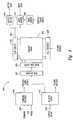
- FIG. 4illustrates a portion of a memory 400 according to an embodiment of the present invention.
- the memory 400includes a write command-data timing circuit 446 according to an embodiment of the invention, for example, the write command-data timing circuit 100 of FIG. 1A .
- the memory 400includes an array 402 of memory cells, which may be, for example, DRAM memory cells, SRAM memory cells, flash memory cells, or some other types of memory cells.
- the memory 400includes a command decoder 406 that receives memory commands through a command bus 408 and generates corresponding control signals within the memory 400 to carry out various memory operations.
- the command decoderfurther receives a memory clock signal CLK and a write clock signal WClk and generates internal clock signals for operation of the memory.
- Row and column address signalsare applied to the memory 400 through an address bus 420 and provided to an address latch 410 .
- the address latchthen outputs a separate column address and a separate row address.
- the row and column addressesare provided by the address latch 410 to a row address decoder 422 and a column address decoder 428 , respectively.
- the column address decoder 428selects bit lines extending through the array 402 corresponding to respective column addresses.
- the row address decoder 422is connected to word line driver 424 that activates respective rows of memory cells in the array 402 corresponding to received row addresses.
- the selected data linee.g., a bit line or bit lines
- a received column addressare coupled to a read/write circuitry 430 to provide read data to a data output buffer 434 via an input-output data bus 440 .
- Write dataare applied to the memory array 402 through a data input buffer 444 and the memory array read/write circuitry 430 .
- a write command-data timing circuit 446is coupled to the data input buffer and receives control/timing signals from the command decoder 406 .
- the timing circuit 446provides timing signals that are used to latch write data of a corresponding write command by generating a correctly timed internal write command signal WE used for capturing write data providing the data to be written to the array 402 .
- the timing circuit 446can provide timing signals for operation where the memory clock signal and the write clock signals are in two different time domains (e.g., different frequencies).
- the command decoder 406responds to memory commands applied to the command bus 408 to perform various operations on the memory array 402 .
- the command decoder 406is used to generate internal control signals to read data from and write data to the memory array 402 .
Landscapes
- Engineering & Computer Science (AREA)
- Microelectronics & Electronic Packaging (AREA)
- Dram (AREA)
Abstract
Description
Claims (23)
Priority Applications (2)
| Application Number | Priority Date | Filing Date | Title |
|---|---|---|---|
| US13/149,435US8441888B2 (en) | 2009-04-01 | 2011-05-31 | Write command and write data timing circuit and methods for timing the same |
| US13/894,069US8760961B2 (en) | 2009-04-01 | 2013-05-14 | Write command and write data timing circuit and methods for timing the same |
Applications Claiming Priority (2)
| Application Number | Priority Date | Filing Date | Title |
|---|---|---|---|
| US12/416,761US7969813B2 (en) | 2009-04-01 | 2009-04-01 | Write command and write data timing circuit and methods for timing the same |
| US13/149,435US8441888B2 (en) | 2009-04-01 | 2011-05-31 | Write command and write data timing circuit and methods for timing the same |
Related Parent Applications (1)
| Application Number | Title | Priority Date | Filing Date |
|---|---|---|---|
| US12/416,761ContinuationUS7969813B2 (en) | 2009-04-01 | 2009-04-01 | Write command and write data timing circuit and methods for timing the same |
Related Child Applications (1)
| Application Number | Title | Priority Date | Filing Date |
|---|---|---|---|
| US13/894,069ContinuationUS8760961B2 (en) | 2009-04-01 | 2013-05-14 | Write command and write data timing circuit and methods for timing the same |
Publications (2)
| Publication Number | Publication Date |
|---|---|
| US20110228625A1 US20110228625A1 (en) | 2011-09-22 |
| US8441888B2true US8441888B2 (en) | 2013-05-14 |
Family
ID=42826078
Family Applications (3)
| Application Number | Title | Priority Date | Filing Date |
|---|---|---|---|
| US12/416,761Active2029-08-08US7969813B2 (en) | 2009-04-01 | 2009-04-01 | Write command and write data timing circuit and methods for timing the same |
| US13/149,435Active2029-07-13US8441888B2 (en) | 2009-04-01 | 2011-05-31 | Write command and write data timing circuit and methods for timing the same |
| US13/894,069ActiveUS8760961B2 (en) | 2009-04-01 | 2013-05-14 | Write command and write data timing circuit and methods for timing the same |
Family Applications Before (1)
| Application Number | Title | Priority Date | Filing Date |
|---|---|---|---|
| US12/416,761Active2029-08-08US7969813B2 (en) | 2009-04-01 | 2009-04-01 | Write command and write data timing circuit and methods for timing the same |
Family Applications After (1)
| Application Number | Title | Priority Date | Filing Date |
|---|---|---|---|
| US13/894,069ActiveUS8760961B2 (en) | 2009-04-01 | 2013-05-14 | Write command and write data timing circuit and methods for timing the same |
Country Status (1)
| Country | Link |
|---|---|
| US (3) | US7969813B2 (en) |
Cited By (19)
| Publication number | Priority date | Publication date | Assignee | Title |
|---|---|---|---|---|
| US20130250701A1 (en)* | 2009-04-01 | 2013-09-26 | Micron Technology, Inc. | Write command and write data timing circuit and methods for timing the same |
| US8644096B2 (en) | 2011-04-25 | 2014-02-04 | Micron Technology, Inc. | Command paths, apparatuses, memories, and methods for providing internal commands to a data path |
| US8913448B2 (en) | 2012-10-25 | 2014-12-16 | Micron Technology, Inc. | Apparatuses and methods for capturing data in a memory |
| US8988966B2 (en) | 2007-03-15 | 2015-03-24 | Micron Technology, Inc. | Circuit, system and method for controlling read latency |
| US9000817B2 (en) | 2012-02-01 | 2015-04-07 | Micron Technology, Inc. | Apparatuses and methods for altering a forward path delay of a signal path |
| US9166579B2 (en) | 2012-06-01 | 2015-10-20 | Micron Technology, Inc. | Methods and apparatuses for shifting data signals to match command signal delay |
| US9183904B2 (en) | 2014-02-07 | 2015-11-10 | Micron Technology, Inc. | Apparatuses, memories, and methods for facilitating splitting of internal commands using a shared signal path |
| US9508417B2 (en) | 2014-02-20 | 2016-11-29 | Micron Technology, Inc. | Methods and apparatuses for controlling timing paths and latency based on a loop delay |
| US9529379B2 (en) | 2006-12-19 | 2016-12-27 | Micron Technology, Inc. | Timing synchronization circuit with loop counter |
| US9531363B2 (en) | 2015-04-28 | 2016-12-27 | Micron Technology, Inc. | Methods and apparatuses including command latency control circuit |
| US9530473B2 (en) | 2014-05-22 | 2016-12-27 | Micron Technology, Inc. | Apparatuses and methods for timing provision of a command to input circuitry |
| US9601170B1 (en) | 2016-04-26 | 2017-03-21 | Micron Technology, Inc. | Apparatuses and methods for adjusting a delay of a command signal path |
| US9734097B2 (en) | 2013-03-15 | 2017-08-15 | Micron Technology, Inc. | Apparatuses and methods for variable latency memory operations |
| US9813067B2 (en) | 2015-06-10 | 2017-11-07 | Micron Technology, Inc. | Clock signal and supply voltage variation tracking |
| US9865317B2 (en) | 2016-04-26 | 2018-01-09 | Micron Technology, Inc. | Methods and apparatuses including command delay adjustment circuit |
| US9997220B2 (en) | 2016-08-22 | 2018-06-12 | Micron Technology, Inc. | Apparatuses and methods for adjusting delay of command signal path |
| US10224938B2 (en) | 2017-07-26 | 2019-03-05 | Micron Technology, Inc. | Apparatuses and methods for indirectly detecting phase variations |
| US20190392888A1 (en)* | 2018-06-21 | 2019-12-26 | Micron Technology, Inc. | Internal write leveling circuitry |
| US10860482B2 (en) | 2013-08-14 | 2020-12-08 | Micron Technology, Inc. | Apparatuses and methods for providing data to a configurable storage area |
Families Citing this family (16)
| Publication number | Priority date | Publication date | Assignee | Title |
|---|---|---|---|---|
| US8984320B2 (en)* | 2011-03-29 | 2015-03-17 | Micron Technology, Inc. | Command paths, apparatuses and methods for providing a command to a data block |
| TWI488192B (en)* | 2011-11-10 | 2015-06-11 | Ind Tech Res Inst | Circuit and method for controlling the write timing of a non-volatile memory |
| WO2013147733A1 (en)* | 2012-03-26 | 2013-10-03 | Intel Corporation | Timing optimization for memory devices employing error detection coded transactions |
| KR102031175B1 (en)* | 2012-06-13 | 2019-10-11 | 에스케이하이닉스 주식회사 | Memory device and operation method of the same |
| US9054675B2 (en) | 2012-06-22 | 2015-06-09 | Micron Technology, Inc. | Apparatuses and methods for adjusting a minimum forward path delay of a signal path |
| US9001594B2 (en) | 2012-07-06 | 2015-04-07 | Micron Technology, Inc. | Apparatuses and methods for adjusting a path delay of a command path |
| US9329623B2 (en)* | 2012-08-22 | 2016-05-03 | Micron Technology, Inc. | Apparatuses, integrated circuits, and methods for synchronizing data signals with a command signal |
| US9076506B2 (en)* | 2012-09-28 | 2015-07-07 | Sandisk Technologies Inc. | Variable rate parallel to serial shift register |
| US9490035B2 (en) | 2012-09-28 | 2016-11-08 | SanDisk Technologies, Inc. | Centralized variable rate serializer and deserializer for bad column management |
| US9293176B2 (en)* | 2014-02-18 | 2016-03-22 | Micron Technology, Inc. | Power management |
| US9892770B2 (en) | 2015-04-22 | 2018-02-13 | Micron Technology, Inc. | Methods and apparatuses for command shifter reduction |
| KR102656696B1 (en)* | 2016-12-06 | 2024-04-12 | 에스케이하이닉스 주식회사 | Semiconductor device |
| US10210918B2 (en) | 2017-02-28 | 2019-02-19 | Micron Technology, Inc. | Apparatuses and methods for determining a phase relationship between an input clock signal and a multiphase clock signal |
| US10090026B2 (en)* | 2017-02-28 | 2018-10-02 | Micron Technology, Inc. | Apparatuses and methods for providing internal memory commands and control signals in semiconductor memories |
| US10269397B2 (en) | 2017-08-31 | 2019-04-23 | Micron Technology, Inc. | Apparatuses and methods for providing active and inactive clock signals |
| TWI658700B (en)* | 2018-07-16 | 2019-05-01 | 創意電子股份有限公司 | Integrated circuit, multi-channels transmission apparatus and signal transmission method thereof |
Citations (43)
| Publication number | Priority date | Publication date | Assignee | Title |
|---|---|---|---|---|
| US6260128B1 (en) | 1997-08-13 | 2001-07-10 | Kabushiki Kaisha Toshiba | Semiconductor memory device which operates in synchronism with a clock signal |
| US20010015924A1 (en) | 1999-12-24 | 2001-08-23 | Kazutami Arimoto | Test interface circuit and semiconductor integrated circuit device including the same |
| US6438055B1 (en) | 1999-10-20 | 2002-08-20 | Fujitsu Limited | Dynamic memory circuit with automatic refresh function |
| US6510095B1 (en) | 2001-09-28 | 2003-01-21 | Fujitsu Limited | Semiconductor memory device for operating in synchronization with edge of clock signal |
| US20030117864A1 (en) | 2001-10-22 | 2003-06-26 | Hampel Craig E. | Phase adjustment apparatus and method for a memory device signaling system |
| US6687185B1 (en) | 2002-08-29 | 2004-02-03 | Micron Technology, Inc. | Method and apparatus for setting and compensating read latency in a high speed DRAM |
| US6744285B2 (en) | 2002-08-08 | 2004-06-01 | Agilent Technologies, Inc. | Method and apparatus for synchronously transferring data across multiple clock domains |
| US6973008B2 (en) | 2003-04-29 | 2005-12-06 | Infineon Technologies Ag | Apparatus for flexible deactivation of word lines of dynamic memory modules and method therefor |
| US6980479B2 (en) | 2003-04-29 | 2005-12-27 | Hynix Semiconductor Inc. | Semiconductor device for domain crossing |
| US6988218B2 (en) | 2002-02-11 | 2006-01-17 | Micron Technology, Inc. | System and method for power saving delay locked loop control by selectively locking delay interval |
| US7042799B2 (en) | 2003-12-30 | 2006-05-09 | Hynix Semiconductor Inc. | Write circuit of double data rate synchronous DRAM |
| US7058799B2 (en) | 2001-06-19 | 2006-06-06 | Micron Technology, Inc. | Apparatus and method for clock domain crossing with integrated decode |
| US20060155948A1 (en) | 2004-10-27 | 2006-07-13 | Hermann Ruckerbauer | Semiconductor memory system and method for data transmission |
| US7170819B2 (en) | 2005-05-04 | 2007-01-30 | Infineon Technologies Ag | Integrated semiconductor memory device for synchronizing a signal with a clock signal |
| US20070033427A1 (en) | 2005-07-19 | 2007-02-08 | International Business Machines Corporation | Power efficient cycle stealing |
| US7187599B2 (en) | 2005-05-25 | 2007-03-06 | Infineon Technologies North America Corp. | Integrated circuit chip having a first delay circuit trimmed via a second delay circuit |
| US20070088903A1 (en) | 2005-10-17 | 2007-04-19 | Samsung Electronics Co., Ltd. | Memory module, memory system and method for controlling the memory system |
| US7209396B2 (en) | 2005-02-28 | 2007-04-24 | Infineon Technologies Ag | Data strobe synchronization for DRAM devices |
| US7269754B2 (en) | 2002-12-30 | 2007-09-11 | Intel Corporation | Method and apparatus for flexible and programmable clock crossing control with dynamic compensation |
| US7280430B2 (en) | 2005-04-30 | 2007-10-09 | Hynix Semiconductor Inc. | Semiconductor memory device |
| US7340632B2 (en) | 2004-01-10 | 2008-03-04 | Hynix Semiconductor Inc. | Domain crossing device |
| US20080080271A1 (en) | 2006-09-29 | 2008-04-03 | Hynix Semiconductor Inc. | Delay selecting circuit for semiconductor memory device |
| US7375560B2 (en) | 2004-08-31 | 2008-05-20 | Micron Technology, Inc. | Method and apparatus for timing domain crossing |
| US7451338B2 (en) | 2005-09-30 | 2008-11-11 | Intel Corporation | Clock domain crossing |
| US7631248B2 (en) | 2004-09-29 | 2009-12-08 | Intel Corporation | Cycle-stealing decoding apparatus, systems, and methods |
| US20090315600A1 (en) | 2008-06-18 | 2009-12-24 | Micron Technologies, Inc. | Locked-loop quiescence apparatus, systems, and methods |
| US20100001762A1 (en) | 2008-07-03 | 2010-01-07 | Hynix Semiconductor, Inc. | Domain crossing circuit and method |
| US7656745B2 (en) | 2007-03-15 | 2010-02-02 | Micron Technology, Inc. | Circuit, system and method for controlling read latency |
| US7660187B2 (en) | 2004-08-04 | 2010-02-09 | Micron Technology, Inc. | Method and apparatus for initialization of read latency tracking circuit in high-speed DRAM |
| US7663946B2 (en) | 2007-07-12 | 2010-02-16 | Hynix Semiconductor Inc. | Semiconductor memory device having on-die-termination device and operation method thereof |
| US7716510B2 (en) | 2006-12-19 | 2010-05-11 | Micron Technology, Inc. | Timing synchronization circuit with loop counter |
| US20100165769A1 (en) | 2008-12-25 | 2010-07-01 | Elpida Memory. Inc. | Semiconductor memory device having auto-precharge function |
| US20100165780A1 (en) | 2008-12-27 | 2010-07-01 | Bains Kuljit S | Dynamic random access memory with shadow writes |
| US7751261B2 (en) | 2007-02-08 | 2010-07-06 | Samsung Electronics Co., Ltd. | Method and apparatus for controlling read latency of high-speed DRAM |
| US20100195429A1 (en) | 2009-02-03 | 2010-08-05 | Nec Electronics Corporation | Semiconductor memory device |
| US7773435B2 (en) | 2008-01-03 | 2010-08-10 | Samsung Electronics Co., Ltd. | Semiconductor memory devices for controlling latency |
| US20100254198A1 (en) | 2009-04-01 | 2010-10-07 | Venkatraghavan Bringivijayaraghavan | Write command and write data timing circuit and methods for timing the same |
| US7826305B2 (en) | 2007-07-10 | 2010-11-02 | Elpida Memory, Inc. | Latency counter, semiconductor memory device including the same, and data processing system |
| US7872924B2 (en) | 2008-10-28 | 2011-01-18 | Micron Technology, Inc. | Multi-phase duty-cycle corrected clock signal generator and memory having same |
| US20110055671A1 (en) | 2009-09-03 | 2011-03-03 | International Business Machines Corporation | Advanced memory device having improved performance, reduced power and increased reliability |
| US7913103B2 (en) | 2007-08-31 | 2011-03-22 | Globalfoundries Inc. | Method and apparatus for clock cycle stealing |
| US7948817B2 (en) | 2009-02-27 | 2011-05-24 | International Business Machines Corporation | Advanced memory device having reduced power and improved performance |
| US20110238941A1 (en) | 2010-03-29 | 2011-09-29 | Freescale Semiconductor, Inc. | Scheduling memory access requests using predicted memory timing and state information |
Family Cites Families (32)
| Publication number | Priority date | Publication date | Assignee | Title |
|---|---|---|---|---|
| US5852640A (en) | 1995-06-26 | 1998-12-22 | Kliza; Phillip S. | Clock distribution apparatus with current sensed skew cancelling |
| US6459313B1 (en) | 1998-09-18 | 2002-10-01 | Lsi Logic Corporation | IO power management: synchronously regulated output skew |
| US6275077B1 (en) | 1999-08-31 | 2001-08-14 | Sun Microsystems, Inc. | Method and apparatus for programmable adjustment of bus driver propagation times |
| KR100459709B1 (en) | 2002-04-03 | 2004-12-04 | 삼성전자주식회사 | Serializer-deserializer circuit having enough set up and hold time margin |
| DE10229460B3 (en) | 2002-07-01 | 2004-01-29 | Texas Instruments Deutschland Gmbh | Voltage follower and ASK demodulator with one voltage follower |
| US7082546B2 (en) | 2002-08-12 | 2006-07-25 | Broadcom Corporation | Low-speed DLL employing a digital phase interpolator based upon a high-speed clock |
| JP3859624B2 (en) | 2003-07-31 | 2006-12-20 | エルピーダメモリ株式会社 | Delay circuit and delay locked loop device |
| KR101090573B1 (en) | 2003-07-31 | 2011-12-08 | 주식회사 아도반테스토 | Clock transfer unit and test equipment |
| US7111185B2 (en) | 2003-12-23 | 2006-09-19 | Micron Technology, Inc. | Synchronization device with delay line control circuit to control amount of delay added to input signal and tuning elements to receive signal form delay circuit |
| US7268605B2 (en) | 2004-06-14 | 2007-09-11 | Rambus, Inc. | Technique for operating a delay circuit |
| JP2007122807A (en) | 2005-10-27 | 2007-05-17 | Elpida Memory Inc | Semiconductor storage device and its adjustment method |
| US7609584B2 (en) | 2005-11-19 | 2009-10-27 | Samsung Electronics Co., Ltd. | Latency control circuit and method thereof and an auto-precharge control circuit and method thereof |
| KR100822578B1 (en) | 2006-04-18 | 2008-04-15 | 주식회사 하이닉스반도체 | Writing device for semiconductor memory device |
| KR100818099B1 (en) | 2006-09-29 | 2008-03-31 | 주식회사 하이닉스반도체 | Data output control circuit and data output control method |
| US7671648B2 (en) | 2006-10-27 | 2010-03-02 | Micron Technology, Inc. | System and method for an accuracy-enhanced DLL during a measure initialization mode |
| KR100834393B1 (en) | 2006-10-31 | 2008-06-04 | 주식회사 하이닉스반도체 | Clock data recovery device. |
| US7593273B2 (en) | 2006-11-06 | 2009-09-22 | Altera Corporation | Read-leveling implementations for DDR3 applications on an FPGA |
| US7590008B1 (en) | 2006-11-06 | 2009-09-15 | Altera Corporation | PVT compensated auto-calibration scheme for DDR3 |
| JP4297159B2 (en) | 2006-12-08 | 2009-07-15 | ソニー株式会社 | Flip-flop and semiconductor integrated circuit |
| US7443216B2 (en) | 2007-02-20 | 2008-10-28 | Micron Technology, Inc. | Trimmable delay locked loop circuitry with improved initialization characteristics |
| US7885365B2 (en) | 2007-08-31 | 2011-02-08 | International Business Machines Corporation | Low-power, low-area high-speed receiver architecture |
| JP4438877B2 (en) | 2008-03-12 | 2010-03-24 | ソニー株式会社 | COMMUNICATION SYSTEM, RECEPTION DEVICE, AND RECEPTION METHOD |
| US7715260B1 (en) | 2008-12-01 | 2010-05-11 | United Microelectronics Corp. | Operating voltage tuning method for static random access memory |
| CN101752009B (en) | 2008-12-16 | 2013-04-17 | 联华电子股份有限公司 | Method for adjusting operating voltage of static random access memory |
| KR20110052941A (en) | 2009-11-13 | 2011-05-19 | 삼성전자주식회사 | Semiconductor device with additive latency |
| US8984320B2 (en) | 2011-03-29 | 2015-03-17 | Micron Technology, Inc. | Command paths, apparatuses and methods for providing a command to a data block |
| US8509011B2 (en) | 2011-04-25 | 2013-08-13 | Micron Technology, Inc. | Command paths, apparatuses, memories, and methods for providing internal commands to a data path |
| US8552776B2 (en) | 2012-02-01 | 2013-10-08 | Micron Technology, Inc. | Apparatuses and methods for altering a forward path delay of a signal path |
| US9166579B2 (en) | 2012-06-01 | 2015-10-20 | Micron Technology, Inc. | Methods and apparatuses for shifting data signals to match command signal delay |
| US9054675B2 (en) | 2012-06-22 | 2015-06-09 | Micron Technology, Inc. | Apparatuses and methods for adjusting a minimum forward path delay of a signal path |
| US9001594B2 (en) | 2012-07-06 | 2015-04-07 | Micron Technology, Inc. | Apparatuses and methods for adjusting a path delay of a command path |
| US9329623B2 (en) | 2012-08-22 | 2016-05-03 | Micron Technology, Inc. | Apparatuses, integrated circuits, and methods for synchronizing data signals with a command signal |
- 2009
- 2009-04-01USUS12/416,761patent/US7969813B2/enactiveActive
- 2011
- 2011-05-31USUS13/149,435patent/US8441888B2/enactiveActive
- 2013
- 2013-05-14USUS13/894,069patent/US8760961B2/enactiveActive
Patent Citations (44)
| Publication number | Priority date | Publication date | Assignee | Title |
|---|---|---|---|---|
| US6260128B1 (en) | 1997-08-13 | 2001-07-10 | Kabushiki Kaisha Toshiba | Semiconductor memory device which operates in synchronism with a clock signal |
| US6438055B1 (en) | 1999-10-20 | 2002-08-20 | Fujitsu Limited | Dynamic memory circuit with automatic refresh function |
| US20010015924A1 (en) | 1999-12-24 | 2001-08-23 | Kazutami Arimoto | Test interface circuit and semiconductor integrated circuit device including the same |
| US7058799B2 (en) | 2001-06-19 | 2006-06-06 | Micron Technology, Inc. | Apparatus and method for clock domain crossing with integrated decode |
| US6510095B1 (en) | 2001-09-28 | 2003-01-21 | Fujitsu Limited | Semiconductor memory device for operating in synchronization with edge of clock signal |
| US20030117864A1 (en) | 2001-10-22 | 2003-06-26 | Hampel Craig E. | Phase adjustment apparatus and method for a memory device signaling system |
| US6988218B2 (en) | 2002-02-11 | 2006-01-17 | Micron Technology, Inc. | System and method for power saving delay locked loop control by selectively locking delay interval |
| US6744285B2 (en) | 2002-08-08 | 2004-06-01 | Agilent Technologies, Inc. | Method and apparatus for synchronously transferring data across multiple clock domains |
| US6687185B1 (en) | 2002-08-29 | 2004-02-03 | Micron Technology, Inc. | Method and apparatus for setting and compensating read latency in a high speed DRAM |
| US7269754B2 (en) | 2002-12-30 | 2007-09-11 | Intel Corporation | Method and apparatus for flexible and programmable clock crossing control with dynamic compensation |
| US6973008B2 (en) | 2003-04-29 | 2005-12-06 | Infineon Technologies Ag | Apparatus for flexible deactivation of word lines of dynamic memory modules and method therefor |
| US6980479B2 (en) | 2003-04-29 | 2005-12-27 | Hynix Semiconductor Inc. | Semiconductor device for domain crossing |
| US7042799B2 (en) | 2003-12-30 | 2006-05-09 | Hynix Semiconductor Inc. | Write circuit of double data rate synchronous DRAM |
| US7340632B2 (en) | 2004-01-10 | 2008-03-04 | Hynix Semiconductor Inc. | Domain crossing device |
| US7660187B2 (en) | 2004-08-04 | 2010-02-09 | Micron Technology, Inc. | Method and apparatus for initialization of read latency tracking circuit in high-speed DRAM |
| US7375560B2 (en) | 2004-08-31 | 2008-05-20 | Micron Technology, Inc. | Method and apparatus for timing domain crossing |
| US7631248B2 (en) | 2004-09-29 | 2009-12-08 | Intel Corporation | Cycle-stealing decoding apparatus, systems, and methods |
| US20060155948A1 (en) | 2004-10-27 | 2006-07-13 | Hermann Ruckerbauer | Semiconductor memory system and method for data transmission |
| US7209396B2 (en) | 2005-02-28 | 2007-04-24 | Infineon Technologies Ag | Data strobe synchronization for DRAM devices |
| US7280430B2 (en) | 2005-04-30 | 2007-10-09 | Hynix Semiconductor Inc. | Semiconductor memory device |
| US7170819B2 (en) | 2005-05-04 | 2007-01-30 | Infineon Technologies Ag | Integrated semiconductor memory device for synchronizing a signal with a clock signal |
| US7187599B2 (en) | 2005-05-25 | 2007-03-06 | Infineon Technologies North America Corp. | Integrated circuit chip having a first delay circuit trimmed via a second delay circuit |
| US20070033427A1 (en) | 2005-07-19 | 2007-02-08 | International Business Machines Corporation | Power efficient cycle stealing |
| US7451338B2 (en) | 2005-09-30 | 2008-11-11 | Intel Corporation | Clock domain crossing |
| US20070088903A1 (en) | 2005-10-17 | 2007-04-19 | Samsung Electronics Co., Ltd. | Memory module, memory system and method for controlling the memory system |
| US20080080271A1 (en) | 2006-09-29 | 2008-04-03 | Hynix Semiconductor Inc. | Delay selecting circuit for semiconductor memory device |
| US7716510B2 (en) | 2006-12-19 | 2010-05-11 | Micron Technology, Inc. | Timing synchronization circuit with loop counter |
| US7751261B2 (en) | 2007-02-08 | 2010-07-06 | Samsung Electronics Co., Ltd. | Method and apparatus for controlling read latency of high-speed DRAM |
| US7656745B2 (en) | 2007-03-15 | 2010-02-02 | Micron Technology, Inc. | Circuit, system and method for controlling read latency |
| US7826305B2 (en) | 2007-07-10 | 2010-11-02 | Elpida Memory, Inc. | Latency counter, semiconductor memory device including the same, and data processing system |
| US7663946B2 (en) | 2007-07-12 | 2010-02-16 | Hynix Semiconductor Inc. | Semiconductor memory device having on-die-termination device and operation method thereof |
| US7913103B2 (en) | 2007-08-31 | 2011-03-22 | Globalfoundries Inc. | Method and apparatus for clock cycle stealing |
| US7773435B2 (en) | 2008-01-03 | 2010-08-10 | Samsung Electronics Co., Ltd. | Semiconductor memory devices for controlling latency |
| US20090315600A1 (en) | 2008-06-18 | 2009-12-24 | Micron Technologies, Inc. | Locked-loop quiescence apparatus, systems, and methods |
| US20100001762A1 (en) | 2008-07-03 | 2010-01-07 | Hynix Semiconductor, Inc. | Domain crossing circuit and method |
| US7872924B2 (en) | 2008-10-28 | 2011-01-18 | Micron Technology, Inc. | Multi-phase duty-cycle corrected clock signal generator and memory having same |
| US20100165769A1 (en) | 2008-12-25 | 2010-07-01 | Elpida Memory. Inc. | Semiconductor memory device having auto-precharge function |
| US20100165780A1 (en) | 2008-12-27 | 2010-07-01 | Bains Kuljit S | Dynamic random access memory with shadow writes |
| US20100195429A1 (en) | 2009-02-03 | 2010-08-05 | Nec Electronics Corporation | Semiconductor memory device |
| US7948817B2 (en) | 2009-02-27 | 2011-05-24 | International Business Machines Corporation | Advanced memory device having reduced power and improved performance |
| US20100254198A1 (en) | 2009-04-01 | 2010-10-07 | Venkatraghavan Bringivijayaraghavan | Write command and write data timing circuit and methods for timing the same |
| US7969813B2 (en)* | 2009-04-01 | 2011-06-28 | Micron Technology, Inc. | Write command and write data timing circuit and methods for timing the same |
| US20110055671A1 (en) | 2009-09-03 | 2011-03-03 | International Business Machines Corporation | Advanced memory device having improved performance, reduced power and increased reliability |
| US20110238941A1 (en) | 2010-03-29 | 2011-09-29 | Freescale Semiconductor, Inc. | Scheduling memory access requests using predicted memory timing and state information |
Non-Patent Citations (9)
| Title |
|---|
| "Interfacing DDR SDRAM with Stratix II Devices", Version 3.2, Altera Corp, Sep. 2008. |
| Lee, "How to Implement DDR SGRAM in Graphic System", Samsung Electric, 1998. |
| Notificiation of International Search Report and Written Opinion dated May 7, 2012 for International Application No. PCT/US2012/027672, May 7, 2012, 1-9. |
| Related U.S. Appl. No, 13/531,341, filed Jun. 22, 2012. |
| Related U.S. Appl. No. 13/074,972, filed Mar. 29, 2011. |
| Related U.S. Appl. No. 13/093,640, filed Apr. 25, 2011. |
| Related U.S. Appl. No. 13/364,198, filed Feb. 1, 2012. |
| Related U.S. Appl. No. 13/486,674, filed Jun. 1, 2012. |
| Related U.S. Appl. No. 13/543,698, filed Jul. 6, 2012. |
Cited By (28)
| Publication number | Priority date | Publication date | Assignee | Title |
|---|---|---|---|---|
| US9529379B2 (en) | 2006-12-19 | 2016-12-27 | Micron Technology, Inc. | Timing synchronization circuit with loop counter |
| US8988966B2 (en) | 2007-03-15 | 2015-03-24 | Micron Technology, Inc. | Circuit, system and method for controlling read latency |
| US10658019B2 (en) | 2007-03-15 | 2020-05-19 | Micron Technology, Inc. | Circuit, system and method for controlling read latency |
| US8760961B2 (en)* | 2009-04-01 | 2014-06-24 | Micron Technology, Inc. | Write command and write data timing circuit and methods for timing the same |
| US20130250701A1 (en)* | 2009-04-01 | 2013-09-26 | Micron Technology, Inc. | Write command and write data timing circuit and methods for timing the same |
| US8644096B2 (en) | 2011-04-25 | 2014-02-04 | Micron Technology, Inc. | Command paths, apparatuses, memories, and methods for providing internal commands to a data path |
| US9000817B2 (en) | 2012-02-01 | 2015-04-07 | Micron Technology, Inc. | Apparatuses and methods for altering a forward path delay of a signal path |
| US9166579B2 (en) | 2012-06-01 | 2015-10-20 | Micron Technology, Inc. | Methods and apparatuses for shifting data signals to match command signal delay |
| US8913448B2 (en) | 2012-10-25 | 2014-12-16 | Micron Technology, Inc. | Apparatuses and methods for capturing data in a memory |
| US9734097B2 (en) | 2013-03-15 | 2017-08-15 | Micron Technology, Inc. | Apparatuses and methods for variable latency memory operations |
| US10740263B2 (en) | 2013-03-15 | 2020-08-11 | Micron Technology, Inc. | Apparatuses and methods for variable latency memory operations |
| US10860482B2 (en) | 2013-08-14 | 2020-12-08 | Micron Technology, Inc. | Apparatuses and methods for providing data to a configurable storage area |
| US9183904B2 (en) | 2014-02-07 | 2015-11-10 | Micron Technology, Inc. | Apparatuses, memories, and methods for facilitating splitting of internal commands using a shared signal path |
| US9508417B2 (en) | 2014-02-20 | 2016-11-29 | Micron Technology, Inc. | Methods and apparatuses for controlling timing paths and latency based on a loop delay |
| US9530473B2 (en) | 2014-05-22 | 2016-12-27 | Micron Technology, Inc. | Apparatuses and methods for timing provision of a command to input circuitry |
| US9531363B2 (en) | 2015-04-28 | 2016-12-27 | Micron Technology, Inc. | Methods and apparatuses including command latency control circuit |
| US9813067B2 (en) | 2015-06-10 | 2017-11-07 | Micron Technology, Inc. | Clock signal and supply voltage variation tracking |
| US10193558B2 (en) | 2015-06-10 | 2019-01-29 | Micron Technology, Inc. | Clock signal and supply voltage variation tracking |
| US10290336B2 (en) | 2016-04-26 | 2019-05-14 | Micron Technology, Inc. | Methods and apparatuses including command delay adjustment circuit |
| US9601170B1 (en) | 2016-04-26 | 2017-03-21 | Micron Technology, Inc. | Apparatuses and methods for adjusting a delay of a command signal path |
| US10755758B2 (en) | 2016-04-26 | 2020-08-25 | Micron Technology, Inc. | Methods and apparatuses including command delay adjustment circuit |
| US9865317B2 (en) | 2016-04-26 | 2018-01-09 | Micron Technology, Inc. | Methods and apparatuses including command delay adjustment circuit |
| US9997220B2 (en) | 2016-08-22 | 2018-06-12 | Micron Technology, Inc. | Apparatuses and methods for adjusting delay of command signal path |
| US11087806B2 (en) | 2016-08-22 | 2021-08-10 | Micron Technology, Inc. | Apparatuses and methods for adjusting delay of command signal path |
| US10224938B2 (en) | 2017-07-26 | 2019-03-05 | Micron Technology, Inc. | Apparatuses and methods for indirectly detecting phase variations |
| US10797708B2 (en) | 2017-07-26 | 2020-10-06 | Micron Technology, Inc. | Apparatuses and methods for indirectly detecting phase variations |
| US20190392888A1 (en)* | 2018-06-21 | 2019-12-26 | Micron Technology, Inc. | Internal write leveling circuitry |
| US10803924B2 (en)* | 2018-06-21 | 2020-10-13 | Micron Technology, Inc. | Internal write leveling circuitry |
Also Published As
| Publication number | Publication date |
|---|---|
| US8760961B2 (en) | 2014-06-24 |
| US20110228625A1 (en) | 2011-09-22 |
| US20130250701A1 (en) | 2013-09-26 |
| US7969813B2 (en) | 2011-06-28 |
| US20100254198A1 (en) | 2010-10-07 |
Similar Documents
| Publication | Publication Date | Title |
|---|---|---|
| US8441888B2 (en) | Write command and write data timing circuit and methods for timing the same | |
| US11150686B2 (en) | Apparatuses for reducing clock path power consumption in low power dynamic random access memory | |
| KR102401526B1 (en) | Apparatus and method for determining a phase relationship between an input clock signal and a polyphase clock signal | |
| JP3013714B2 (en) | Semiconductor storage device | |
| KR101653035B1 (en) | Command paths, apparatuses and methods for providing a command to a data block | |
| US7061823B2 (en) | Limited output address register technique providing selectively variable write latency in DDR2 (double data rate two) integrated circuit memory devices | |
| US8913448B2 (en) | Apparatuses and methods for capturing data in a memory | |
| KR100909805B1 (en) | Multiport memory device | |
| CN110366755B (en) | Apparatus and method for providing internal memory command and control signal in semiconductor memory | |
| JP3183321B2 (en) | Semiconductor storage device | |
| US8477543B2 (en) | Data input circuit with a valid strobe signal generation circuit | |
| US9111607B2 (en) | Multiple data rate memory with read timing information | |
| US7613069B2 (en) | Address latch circuit of semiconductor memory device | |
| CN101645294A (en) | Control circuit of read operation for semiconductor memory apparatus | |
| US8773928B2 (en) | Command latency systems and methods | |
| CN113129958A (en) | Apparatus and method for wide clock frequency range command path | |
| US9183900B2 (en) | Data paths using a first signal to capture data and a second signal to output data and methods for providing data | |
| US6201756B1 (en) | Semiconductor memory device and write data masking method thereof | |
| KR100654125B1 (en) | Data output device of semiconductor memory device | |
| US20050157827A1 (en) | Method and circuit for writing double data rate (DDR) sampled data in a memory device | |
| CN110097902B (en) | Read-write control module and method for same port and dual-port memory | |
| JP3859885B2 (en) | Semiconductor memory device | |
| KR101869692B1 (en) | Data output circuit | |
| KR100976406B1 (en) | Flip-flop and semiconductor memory device comprising the same | |
| WO2025007452A1 (en) | Control circuit and memory |
Legal Events
| Date | Code | Title | Description |
|---|---|---|---|
| FEPP | Fee payment procedure | Free format text:PAYOR NUMBER ASSIGNED (ORIGINAL EVENT CODE: ASPN); ENTITY STATUS OF PATENT OWNER: LARGE ENTITY | |
| STCF | Information on status: patent grant | Free format text:PATENTED CASE | |
| AS | Assignment | Owner name:U.S. BANK NATIONAL ASSOCIATION, AS COLLATERAL AGENT, CALIFORNIA Free format text:SECURITY INTEREST;ASSIGNOR:MICRON TECHNOLOGY, INC.;REEL/FRAME:038669/0001 Effective date:20160426 Owner name:U.S. BANK NATIONAL ASSOCIATION, AS COLLATERAL AGEN Free format text:SECURITY INTEREST;ASSIGNOR:MICRON TECHNOLOGY, INC.;REEL/FRAME:038669/0001 Effective date:20160426 | |
| AS | Assignment | Owner name:MORGAN STANLEY SENIOR FUNDING, INC., AS COLLATERAL AGENT, MARYLAND Free format text:PATENT SECURITY AGREEMENT;ASSIGNOR:MICRON TECHNOLOGY, INC.;REEL/FRAME:038954/0001 Effective date:20160426 Owner name:MORGAN STANLEY SENIOR FUNDING, INC., AS COLLATERAL Free format text:PATENT SECURITY AGREEMENT;ASSIGNOR:MICRON TECHNOLOGY, INC.;REEL/FRAME:038954/0001 Effective date:20160426 | |
| FPAY | Fee payment | Year of fee payment:4 | |
| AS | Assignment | Owner name:U.S. BANK NATIONAL ASSOCIATION, AS COLLATERAL AGENT, CALIFORNIA Free format text:CORRECTIVE ASSIGNMENT TO CORRECT THE REPLACE ERRONEOUSLY FILED PATENT #7358718 WITH THE CORRECT PATENT #7358178 PREVIOUSLY RECORDED ON REEL 038669 FRAME 0001. ASSIGNOR(S) HEREBY CONFIRMS THE SECURITY INTEREST;ASSIGNOR:MICRON TECHNOLOGY, INC.;REEL/FRAME:043079/0001 Effective date:20160426 Owner name:U.S. BANK NATIONAL ASSOCIATION, AS COLLATERAL AGEN Free format text:CORRECTIVE ASSIGNMENT TO CORRECT THE REPLACE ERRONEOUSLY FILED PATENT #7358718 WITH THE CORRECT PATENT #7358178 PREVIOUSLY RECORDED ON REEL 038669 FRAME 0001. ASSIGNOR(S) HEREBY CONFIRMS THE SECURITY INTEREST;ASSIGNOR:MICRON TECHNOLOGY, INC.;REEL/FRAME:043079/0001 Effective date:20160426 | |
| AS | Assignment | Owner name:JPMORGAN CHASE BANK, N.A., AS COLLATERAL AGENT, ILLINOIS Free format text:SECURITY INTEREST;ASSIGNORS:MICRON TECHNOLOGY, INC.;MICRON SEMICONDUCTOR PRODUCTS, INC.;REEL/FRAME:047540/0001 Effective date:20180703 Owner name:JPMORGAN CHASE BANK, N.A., AS COLLATERAL AGENT, IL Free format text:SECURITY INTEREST;ASSIGNORS:MICRON TECHNOLOGY, INC.;MICRON SEMICONDUCTOR PRODUCTS, INC.;REEL/FRAME:047540/0001 Effective date:20180703 | |
| AS | Assignment | Owner name:MICRON TECHNOLOGY, INC., IDAHO Free format text:RELEASE BY SECURED PARTY;ASSIGNOR:U.S. BANK NATIONAL ASSOCIATION, AS COLLATERAL AGENT;REEL/FRAME:047243/0001 Effective date:20180629 | |
| AS | Assignment | Owner name:MICRON TECHNOLOGY, INC., IDAHO Free format text:RELEASE BY SECURED PARTY;ASSIGNOR:MORGAN STANLEY SENIOR FUNDING, INC., AS COLLATERAL AGENT;REEL/FRAME:050937/0001 Effective date:20190731 | |
| AS | Assignment | Owner name:MICRON SEMICONDUCTOR PRODUCTS, INC., IDAHO Free format text:RELEASE BY SECURED PARTY;ASSIGNOR:JPMORGAN CHASE BANK, N.A., AS COLLATERAL AGENT;REEL/FRAME:051028/0001 Effective date:20190731 Owner name:MICRON TECHNOLOGY, INC., IDAHO Free format text:RELEASE BY SECURED PARTY;ASSIGNOR:JPMORGAN CHASE BANK, N.A., AS COLLATERAL AGENT;REEL/FRAME:051028/0001 Effective date:20190731 | |
| MAFP | Maintenance fee payment | Free format text:PAYMENT OF MAINTENANCE FEE, 8TH YEAR, LARGE ENTITY (ORIGINAL EVENT CODE: M1552); ENTITY STATUS OF PATENT OWNER: LARGE ENTITY Year of fee payment:8 | |
| MAFP | Maintenance fee payment | Free format text:PAYMENT OF MAINTENANCE FEE, 12TH YEAR, LARGE ENTITY (ORIGINAL EVENT CODE: M1553); ENTITY STATUS OF PATENT OWNER: LARGE ENTITY Year of fee payment:12 |