US8441411B2 - Integrated electronic device and methods of making the same - Google Patents
Integrated electronic device and methods of making the sameDownload PDFInfo
- Publication number
- US8441411B2 US8441411B2US12/669,067US66906708AUS8441411B2US 8441411 B2US8441411 B2US 8441411B2US 66906708 AUS66906708 AUS 66906708AUS 8441411 B2US8441411 B2US 8441411B2
- Authority
- US
- United States
- Prior art keywords
- substrate
- layer
- providing
- cathode
- rfid
- Prior art date
- Legal status (The legal status is an assumption and is not a legal conclusion. Google has not performed a legal analysis and makes no representation as to the accuracy of the status listed.)
- Active, expires
Links
Images


Classifications
- G—PHYSICS
- G06—COMPUTING OR CALCULATING; COUNTING
- G06K—GRAPHICAL DATA READING; PRESENTATION OF DATA; RECORD CARRIERS; HANDLING RECORD CARRIERS
- G06K19/00—Record carriers for use with machines and with at least a part designed to carry digital markings
- G06K19/06—Record carriers for use with machines and with at least a part designed to carry digital markings characterised by the kind of the digital marking, e.g. shape, nature, code
- G06K19/067—Record carriers with conductive marks, printed circuits or semiconductor circuit elements, e.g. credit or identity cards also with resonating or responding marks without active components
- G06K19/07—Record carriers with conductive marks, printed circuits or semiconductor circuit elements, e.g. credit or identity cards also with resonating or responding marks without active components with integrated circuit chips
- G06K19/077—Constructional details, e.g. mounting of circuits in the carrier
- G06K19/07749—Constructional details, e.g. mounting of circuits in the carrier the record carrier being capable of non-contact communication, e.g. constructional details of the antenna of a non-contact smart card
- G—PHYSICS
- G06—COMPUTING OR CALCULATING; COUNTING
- G06K—GRAPHICAL DATA READING; PRESENTATION OF DATA; RECORD CARRIERS; HANDLING RECORD CARRIERS
- G06K19/00—Record carriers for use with machines and with at least a part designed to carry digital markings
- G06K19/06—Record carriers for use with machines and with at least a part designed to carry digital markings characterised by the kind of the digital marking, e.g. shape, nature, code
- G06K19/067—Record carriers with conductive marks, printed circuits or semiconductor circuit elements, e.g. credit or identity cards also with resonating or responding marks without active components
- G06K19/07—Record carriers with conductive marks, printed circuits or semiconductor circuit elements, e.g. credit or identity cards also with resonating or responding marks without active components with integrated circuit chips
- G06K19/0701—Record carriers with conductive marks, printed circuits or semiconductor circuit elements, e.g. credit or identity cards also with resonating or responding marks without active components with integrated circuit chips at least one of the integrated circuit chips comprising an arrangement for power management
- G06K19/0702—Record carriers with conductive marks, printed circuits or semiconductor circuit elements, e.g. credit or identity cards also with resonating or responding marks without active components with integrated circuit chips at least one of the integrated circuit chips comprising an arrangement for power management the arrangement including a battery
- G—PHYSICS
- G06—COMPUTING OR CALCULATING; COUNTING
- G06K—GRAPHICAL DATA READING; PRESENTATION OF DATA; RECORD CARRIERS; HANDLING RECORD CARRIERS
- G06K19/00—Record carriers for use with machines and with at least a part designed to carry digital markings
- G06K19/06—Record carriers for use with machines and with at least a part designed to carry digital markings characterised by the kind of the digital marking, e.g. shape, nature, code
- G06K19/067—Record carriers with conductive marks, printed circuits or semiconductor circuit elements, e.g. credit or identity cards also with resonating or responding marks without active components
- G06K19/07—Record carriers with conductive marks, printed circuits or semiconductor circuit elements, e.g. credit or identity cards also with resonating or responding marks without active components with integrated circuit chips
- G06K19/077—Constructional details, e.g. mounting of circuits in the carrier
- G06K19/07718—Constructional details, e.g. mounting of circuits in the carrier the record carrier being manufactured in a continuous process, e.g. using endless rolls
- H—ELECTRICITY
- H01—ELECTRIC ELEMENTS
- H01M—PROCESSES OR MEANS, e.g. BATTERIES, FOR THE DIRECT CONVERSION OF CHEMICAL ENERGY INTO ELECTRICAL ENERGY
- H01M10/00—Secondary cells; Manufacture thereof
- H01M10/04—Construction or manufacture in general
- H01M10/0436—Small-sized flat cells or batteries for portable equipment
- Y—GENERAL TAGGING OF NEW TECHNOLOGICAL DEVELOPMENTS; GENERAL TAGGING OF CROSS-SECTIONAL TECHNOLOGIES SPANNING OVER SEVERAL SECTIONS OF THE IPC; TECHNICAL SUBJECTS COVERED BY FORMER USPC CROSS-REFERENCE ART COLLECTIONS [XRACs] AND DIGESTS
- Y02—TECHNOLOGIES OR APPLICATIONS FOR MITIGATION OR ADAPTATION AGAINST CLIMATE CHANGE
- Y02E—REDUCTION OF GREENHOUSE GAS [GHG] EMISSIONS, RELATED TO ENERGY GENERATION, TRANSMISSION OR DISTRIBUTION
- Y02E60/00—Enabling technologies; Technologies with a potential or indirect contribution to GHG emissions mitigation
- Y02E60/10—Energy storage using batteries
- Y—GENERAL TAGGING OF NEW TECHNOLOGICAL DEVELOPMENTS; GENERAL TAGGING OF CROSS-SECTIONAL TECHNOLOGIES SPANNING OVER SEVERAL SECTIONS OF THE IPC; TECHNICAL SUBJECTS COVERED BY FORMER USPC CROSS-REFERENCE ART COLLECTIONS [XRACs] AND DIGESTS
- Y02—TECHNOLOGIES OR APPLICATIONS FOR MITIGATION OR ADAPTATION AGAINST CLIMATE CHANGE
- Y02P—CLIMATE CHANGE MITIGATION TECHNOLOGIES IN THE PRODUCTION OR PROCESSING OF GOODS
- Y02P70/00—Climate change mitigation technologies in the production process for final industrial or consumer products
- Y02P70/50—Manufacturing or production processes characterised by the final manufactured product
- Y—GENERAL TAGGING OF NEW TECHNOLOGICAL DEVELOPMENTS; GENERAL TAGGING OF CROSS-SECTIONAL TECHNOLOGIES SPANNING OVER SEVERAL SECTIONS OF THE IPC; TECHNICAL SUBJECTS COVERED BY FORMER USPC CROSS-REFERENCE ART COLLECTIONS [XRACs] AND DIGESTS
- Y10—TECHNICAL SUBJECTS COVERED BY FORMER USPC
- Y10T—TECHNICAL SUBJECTS COVERED BY FORMER US CLASSIFICATION
- Y10T29/00—Metal working
- Y10T29/49—Method of mechanical manufacture
- Y10T29/49002—Electrical device making
- Y10T29/49016—Antenna or wave energy "plumbing" making
- Y10T29/49018—Antenna or wave energy "plumbing" making with other electrical component
Definitions
- an electrical devicecomprising an electrical apparatus including: a base substrate having a first side and a second side, an antenna and/or an electrical component provided on the second side of the substrate, and on the first side of the substrate an electrochemical cell and/or battery that is electrically connected to the antenna and/or electrical component on the second side of the substrate, such as by means of through holes, wherein the cell or battery is for providing electrical energy to the electrical apparatus.
- a method of manufacturing an active RFID device including a flat electrochemical cell for generating an electrical currentincluding the steps of providing a first substrate and a second substrate. At least one of the first and second substrates includes a plurality of layers, and the first substrate including a first side and a second side.
- An active RFID assemblyis provided on the second side of the first substrate, including a RFID antenna, an active RFID element in communication with the RFID antenna, and a plurality of electrical contacts in electrical communication with the active RFID element.
- a cathode layeris provided on the first side of the first substrate, and an anode layer is provided on the first side of the first substrate.
- An electrolyte layerincluding a viscous liquid in contact with the cathode layer and also in contact with the anode layer.
- a frameis provided on the first side of the first substrate to form an inner space containing the electrolyte, and also containing at least a major portion of the cathode layer and at least a major portion of the anode layer within the inner space.
- the cathode layer, anode layer, and the plurality of electrical contactsare electrically coupled, and the second substrate is connected to the first substrate to substantially seal the inner space containing the cathode layer, the anode layer, and the electrolyte layer.
- a method of manufacturing an active RFID device including a flat electrochemical cell for generating an electrical currentincludes the steps of providing a first substrate and a second substrate. At least one of the first and second substrates includes a web having a plurality of layers, and the first substrate includes a first side and a second side.
- An active RFID assemblyis provided on the second side of the first substrate, including the steps of (i) providing an active RFID element on the second side of the first substrate; and (ii) printing an RFID antenna and a plurality of electrical contacts on the second side of the first substrate so as to be in electrical contact with the active RFID element.
- Each of the RFID antenna and plurality of electrical contactsinclude a cured or dried ink.
- a cathode collector layeris printed on a first side of the first substrate.
- a cathode layeris printed on the first side of the first substrate, and an anode layer is laminated on the first side of the first substrate.
- An electrolyte layeris provided including a viscous liquid in contact with the cathode layer and also in contact with the anode layer.
- a frameis provided on the first side of the first substrate to form an inner space containing the electrolyte, and also containing at least a major portion of the cathode layer and at least a major portion of the anode layer within the inner space.
- the cathode layer via the cathode collector layer, the anode layer, and the plurality of electrical contactsare electrically coupled, and the second substrate is connected to the first substrate to substantially seal the inner space containing the cathode layer, the anode layer, and the electrolyte layer.
- an active RFID deviceincluding a flat electrochemical cell for generating an electrical current.
- the active RFID deviceincludes a first substrate including of a plurality of laminated layers and defining a first side and a second side, and a second substrate.
- An active RFID assemblyis provided on the second side of the first substrate, including a RFID antenna, an active RFID element in communication with the RFID antenna, and a plurality of electrical contacts in electrical communication with the active RFID element.
- a cathode layeris provided on the first side of the first substrate, and an anode layer is provided on the first side of the first substrate.
- An electrolyte layerincludes a viscous liquid in contact with the cathode layer and also in contact with the anode layer.
- a frameis interposed between the first and second substrate to connect and seal the first substrate to the second substrate to form an inner space containing the electrolyte, and also containing at least a major portion of the cathode layer and at least a major portion of the anode layer within the inner space. At least one of the anode layer and the cathode layer include a cured or dried ink.
- An electrical coupler assemblyprovides electrical communication between the cathode layer, the anode layer, and the plurality of electrical contacts.
- a method of manufacturing an active RFID device including a flat electrochemical cell for generating an electrical currentincludes the steps of providing a first substrate including a first side and a second side, providing an active RFID assembly on said second side of said first substrate, providing a cathode collector layer on said first side of said first substrate, providing a cathode layer on said first side of said first substrate, and providing an anode layer on said first side of said first substrate.
- the methodfurther includes the steps of providing an electrolyte layer in contact with said cathode layer and also in contact with said anode layer, and electrically coupling the cathode layer via the cathode collector layer, the anode layer, and the active RFID assembly through the first substrate.
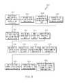
- FIG. 1illustrates an example RFID assembly provided on a second side of an example first substrate
- FIG. 2illustrates an example power source located on a first side of the first substrate
- FIG. 2Aillustrates a cross section view of the unit cell taken through line 2 A- 2 A of FIG. 2 ;
- FIG. 3illustrates a plurality of RFID assemblies provided on a second side of a first substrate web
- FIG. 4illustrates a plurality of completed RFID devices stored on an example roll
- FIG. 5illustrates a partial sectional view of the first substrate
- FIG. 6illustrates a partial sectional view of an example spacer
- FIG. 7illustrates a partial sectional view of an example anode layer
- FIG. 8illustrates a top view of an example spacer web
- FIG. 9illustrates a flow diagram of one example method of manufacturing the example RFID device
- FIG. 10illustrates a plurality of example steps of the method of FIG. 9 ;
- FIG. 11illustrates another plurality of example steps of the method of FIG. 9 ;
- FIG. 12illustrates still yet another plurality of example steps of the method of FIG. 9 ;
- FIG. 13illustrates a schematic view of an example manufacturing process utilizing a generally continuous web.
- the inventionis an electronic device and method of manufacturing said electronic device by integrating an electrical circuit, antenna or skin patch electrodes with one or more cells/batteries to power the device.
- the methodapplies both an electronic device and its power source to a single substrate.
- the electronic device and its power sourcecan share a single substrate to simplify the manufacturing process to provide reduced costs, greater efficiency, and increased economies of scale.
- the circuit and a batteryare typically printed and/or laminated on a continuous, flexible substrate web, and may be formed into a roll or the like.
- the individual devicescan be removed from the roll, such as one at a time. For example, the devices can be cut from the roll, and/or perforations of the flexible substrate roll can be provided for easy tear off.
- the apparatuscan include one or more electrical components, such as an antenna and/or a processor, for example.
- the multiple facets of this inventioncould be used in the total package described and/or they could be used individually or in any combination.
- the present inventionrelates to thin, printed electrochemical cells and/or batteries comprising a plurality of such cells.
- Such cellseach typically include at least a first electrode including a first electrochemical layer (e.g., a cathode), a second electrode including a second electrochemical layer (e.g., an anode), and an electrolyte that interacts with the electrodes to create an electrical current. All of the first and second electrodes and the electrolyte are typically contained within some structure which provides an external electrical access to the electrodes for providing an electrical current supply to some device.
- One method of mass-producing such cellsincludes depositing aqueous and/or non-aqueous solvent inks and/or other coatings in a pattern on a special substrate, such as a laminated polymeric film layer, for example.
- the depositingcan be by means of, for example, printing electrochemical inks and/or laminating a metallic foil, such as a zinc foil, for example, on one or more high-speed web printing presses, especially if the desired volumes are very high. If volumes are relatively lower, say in the quantities of only about several million or less, then relatively slower methods such as web printing with flat bed screens could be appropriate. If the volumes are even lower, such as hundreds or thousands, then a sheet-fed flat bed printing press may be utilized, for example. Still, various printing methods can be used for various desired quantities.
- the cellscan be completed (e.g., sealed, die cut, stacked and/or perforated and wound into a roll, or stacked if sheets are used on a printing press).
- This cell manufacturing processcan also be utilized for integrating one or more individual cells with an actual electronic application, or into batteries comprising multiple cells connected in series or parallel, or some combination of the two. Examples of such devices and corresponding processes will be described later, but many additional embodiments are also contemplated.
- the inventionmay be described as a printed, flexible, and thin electrochemical cell.
- a cellcan include, for example, a lower film substrate that can utilize a special polymer laminate that has special features, possibly including, for example, a high moisture barrier layer in the center that is surrounded by polymer films on both sides.
- a special polymer laminatethat has special features, possibly including, for example, a high moisture barrier layer in the center that is surrounded by polymer films on both sides.
- one or both outside surfacescan be made to be print receptive for printing information, logos, instructions, identifications, serial numbers, graphics, or other information or images, as desired.
- the inner ply of the substratecould also feature a heat-sealing layer that might be co-extruded on the side opposite the barrier coating.
- a portion of the inner surface of a lower substrate layer of a cell of at least some embodimentscould utilize a cathode current collector, such as carbon, for example, printed or coated or otherwise applied on a portion of the film substrate.
- a cathode current collectorsuch as carbon, for example, printed or coated or otherwise applied on a portion of the film substrate.
- this collectorcan also be printed a layer of a relatively highly conductive ink, such as silver, nickel, or tin, for example, to improve the conductivity to the application connection, if desired.
- a relatively highly conductive inksuch as silver, nickel, or tin, for example
- a water-based ink electrochemical layeris printed as the cathode.
- a cathode layercan include, for example, manganese dioxide (MnO 2 ), carbon, and a polymer binder. Other formulations for the cathode layer can also be utilized with or without any of these materials. If a cathode collector layer is used, which may or may not form a portion of the cathode layer, the cathode electrochemical layer will be printed on at least a portion of the cathode current collector, which is printed or otherwise applied first to the substrate.
- adjacent to the cathode collectorat a spacing of about 0.050′′, can be placed a narrow strip of zinc foil as the anode.
- Other anode compositionsare also possible, such as an ink layer including zinc or some other proper material, for example.
- a dry-film adhesive layerpossibly using a release liner, can be applied to the zinc foil.
- the zinc foilcan then be laminated to the base substrate.
- a starch ink or similar materialprinted over one or both the anode and cathode.
- the starch inkcan act as an electrolyte absorber to keep the electrodes “wet” after an aqueous electrolyte solution is added to the cell.
- This starch inkcould also include the electrolyte salts and the water used for the cell reaction.
- a paper layer over the anode and cathodecould be used in place of the printed starch.
- a cell “picture frame”can be added. This could be done using a number of different methods. One method is to print this cell picture frame with a dielectric ink, for example. Another method is to utilize a polymer sheet or a laminated polymer sheet that includes adhesive layers, that is stamped, die cut, laser cut or similar methods to form the appropriate “pockets” (inner space or spaces) to house materials of each unit cell.
- a sealing or caulking adhesivecould be printed on the substrate, such as in the same pattern as the cell frame, for example, prior to the frame being printed or prior to the polymer sheets being inserted, for example.
- This sealing or caulking materialcould be pressure sensitive, and/or heat sensitive, for example, such as Acheson Colloids' PM040, for example, or any other type of material that would facilitate sealing to both surfaces.
- a heat sensitive sealing adhesivecan be printed on top of the frame to allow good sealing of the top substrate to the cell frame.
- This cell picture framecould also comprise a polymer film or a laminated film of about 0.015′′ thick (range of about 0.003′′-0.050′′) that is pre-punched and then laminated in registration to match the preprinted caulking adhesive layer described above.
- Zinc chloridecan be chosen as the electrolyte, for at least some embodiments, in the concentration range of about 18%-45% by weight, for example. In one example, about 27% may be preferred.
- the electrolytecan be added, for example, to the open cell. To facilitate processing on the line, this electrolyte, or a different electrolyte, could be thickened with, for example, CMC at about a level of about 0.6 wgt % (range of about 0.05%-1.0%).
- electrolyte formulationssuch as ammonium chloride (NH 4 Cl), mixtures of zinc chloride (ZnCl 2 ) and ammonium chloride (NH 4 Cl), zinc acetate (Zn(C 2 H 2 O 2 )), zinc bromide (ZnBr 2 ), zinc fluoride (ZnF 2 ), zinc tartrate (ZnC 4 H 4 O 6 .H 2 O), zinc per-chlorate Zn(ClO 4 ) 2 .6H 2 O), potassium hydroxide, sodium hydroxide, or organics, for example, could also be used.
- ammonium chlorideNH 4 Cl
- mixtures of zinc chlorideZnCl 2
- ammonium chlorideNH 4 Cl
- zinc acetateZn(C 2 H 2 O 2
- zinc bromideZnBr 2
- zinc fluorideZnF 2
- zinc tartrateZnC 4 H 4 O 6 .H 2 O
- Zinc chloridemay be the electrolyte of choice, providing excellent electrical performance for ordinary environmental conditions normally encountered.
- any of the above mentioned alternative electrolytes, among others,could be used in concentrations (by weight), for example, within the range of about 18%-45%, with the range of about 25%-35% used for at least some other embodiments.
- Such compositionscould also provide acceptable performance under ordinary environmental conditions.
- electrolytes other than of zinc chloridecan provide improved cell/battery electrical performance under some differing environmental conditions.
- about 32% by weight zinc acetate (F.P.—freezing point—about 28° C.)exhibits a lower freezing point than about 32% by weight zinc chloride (F.P. about ⁇ 23° C.). Both of these solutions exhibit a lower freezing point than of about 27% zinc chloride (F.P. about ⁇ 18° C.).
- Other zinc acetate concentrationse.g. about 18-45 or about 25-35 weight percent, also exhibit reduced freezing points.
- electrolyte formulationsas substitutes for zinc chloride, or in various mixtures used in cells, can allow for improved performance at low temperatures.
- low temperaturei.e. below about ⁇ 20° C.
- This type of electrochemical cell performance improvement at low temperaturecan be utilized in the growing business of battery assisted RFID tags, for example, and/or other transient (transportable) electrically operated devices, such as smart active labels and temperature tags, for example, which may be used in cold environments.
- tags and/or labelsmight require electrochemical cells and/or batteries to operate effectively at temperatures at, or even below, ⁇ 20° C., such as at about ⁇ 23° C., about ⁇ 27° C., or even at about ⁇ 30° C. or less.
- the zinc acetate concentration in the range of about 31-33is often acceptable, although ranges of about 30-34, about 28-36, about 26-38, and even about 25-40, weight percent, could also be utilized.
- the construction of the printed starch layer with the addition of the aqueous electrolytecould be replaced, for example, by a printable viscous liquid (which could include a gel, or some other viscous material) that effectively covers at least a portion of each electrode.
- a printable viscous liquidwhich could include a gel, or some other viscous material
- One such printable gelis described in United States Patent Publication 2003/0165744A1, published on Sep. 4, 2003, and incorporated herein by reference.
- These viscous formulationscould, for example, utilize the electrolyte formulas and concentrations previously discussed.
- the upper substrate of a cell packagecould utilize a special laminated polymeric film, which has an edge that extends beyond the internal cell/battery components onto the cell frame.
- the upper layeris sealed around the edges of the cell frame by means of a pressure sensitive adhesive (PSA), and/or with the heat sensitive sealing adhesive that was previously printed, thus confining the internal components within the cell frame.
- PSApressure sensitive adhesive
- the above-described constructionscan be wet cell constructions; however, using a similar cell construction, the present invention could be also be made into a reserve cell construction, which has the benefit of providing extended shelf life prior to the application of a liquid.
- the printable, flexible, zinc chloride thin cellcan be made environmentally friendly. Such a construction could be utilized which does not require the use of harmful components, such as mercury or cadmium, for example. Old and/or depleted cells of this design could thus be disposed using regular waste removal procedures.
- the devices for which this technology can be usedare extensive. Devices that utilize relatively low power or a limited life of one to three years, and possibly longer, could function utilizing a thin cell/battery according to the invention.
- the cell of the inventionas explained in the above paragraphs and below, can often be inexpensively mass-produced so that it can be used in a disposable product, for example. The low cost allows for applications that previously were not cost effective.
- the electrochemical cell/battery according to the inventionmight have one or more of the following advantages:
- each RFID tagmay include a unique code that specifically identifies it.
- Illustrative information provided by each RFID tagmay include, e.g., an identifier, a serial number, a part type, manufacturer information, etc.
- an RFID tagmay be an electronic circuit adapted to receive incoming radio frequency energy through its antenna, and operate that circuitry to modulate a radio frequency signal to transmit data out through the antenna.
- the RFID tagcan be passive such that it uses a portion of the incoming radio frequency energy to power its own circuitry, or alternatively the RFID tag can be active such that it is coupled to a power source that at least partially powers its own circuitry. However, an active RFID tag can still utilize a portion of the incoming radio frequency energy to power its own circuitry.
- An RFID tagmay also contain circuitry to perform additional operations, such as logic circuitry, memory, sensors, etc. The RFID tag may use any feasible RFID technology currently existing or yet to be developed.
- the inventioncan utilize multiple webs. It is to be understood that the multiple webs can be generally continuous, and can be utilized with known web manufacturing equipment.
- a first webcan be relatively thin, such as ⁇ 0.002′′-0.010′′ and preferably about 0.003-0.006′′, flexible base substrate including a multi-ply laminated structure or single ply material.
- the multi-ply structurecan include five layers.
- the single ply materialcan include various materials, such as Kapton or polyester.
- a second webcan be a relatively thick laminated structure including a PVC or Polyester film that is about 0.005-0.030′′ thick, and preferably about 0.010-0.015′′ thick.
- the second webcan have a layer of pressure sensitive adhesive at about 1-5 mils thick on one side. After this laminated structure of the second web is completed, it can be applied to the first web.
- the second webcan be pattern cut using any type of mechanical means to allow for cavities for the cells active materials as well as an optional cavity for the cell/battery contacts.
- a third webcan be a relatively thin laminated structure the same and/or similar to the first web. The completed three web structure may have a pressure sensitive adhesive on either side to allow the individual device assembly to be applied as a label.
- the cell/batterymay be of the thin cell type, such as disclosed in co-pending application Ser. No. 11/110,202, filed on Apr. 20, 2005 and incorporated herein by reference, and/or the cells disclosed in co-pending application Ser. No. 11/378,520, filed on Mar. 17, 2006, and also incorporated herein by reference.
- the various conductive inks described hereincould be based on many types of conductive materials such as carbon, silver, nickel, silver coated copper, copper, silver chloride, zinc and/or mixtures of these.
- conductive materialssuch as carbon, silver, nickel, silver coated copper, copper, silver chloride, zinc and/or mixtures of these.
- Acheson ColloidsPort Huron, Mich.
- many antennas that might be part of the printed circuitrycan be made by etching aluminum, copper or similar type metallic foils that are laminated on a polymer such as Kapton substrate. This could be done with many types (sizes and frequencies) of antennas whether they are etched or printed. As will be discussed herein, this can be beneficial for the use of etched foil antennas, though other variants are also contemplated.
- a second side 1003 of a first substrate 1000can be the base substrate of an electronic device 99 , such as an RFID assembly, an integrated circuit, a semiconductors, various electronic components, etc.
- the electronic device 99can include an RFID device having an RFID antenna and chip assembly including antenna coils 101 , a IC chip 102 that uses a power source, and/or many other features and circuitry 103 that may be desired for an active RFID application.
- the RFID assembly 99can also include various associated circuitry, such as a time/temperature sensor, memory, etc.
- the various elements of the RFID assembly 99can be printed on the first substrate 1000 , including the IC chip 102 .
- the IC chip 102can be provided in various other manners.
- the IC chip 102can be coupled to the first substrate 1000 using “flip chip” structure (i.e., controlled collapse chip connection), and/or straps or interposers, or the like.
- the IC chip 102can be provided to the first substrate 1000 before, during, or even after the other structure of the RFID assembly 99 , such as the antenna coils 101 .
- the RFID assembly 99can also include a negative contact 106 and a positive contact 107 , for electrical coupling to a power source (see FIG. 2 ), located on a second side 1003 of the first substrate 1000 .
- the first substratecan be a single layer of Kapton, or preferably a multi-ply (such as five ply) laminated polyester structure.
- the power source negative contact 106 as well as the positive contact 107can include a plurality of apertures, such as a set of through-holes 104 and 105 (or vias, electrical jumpers, etc.), respectively, to make contact to the power source, which can be a cell an/or battery which is assembled on the second side of the base substrate.
- dielectric pads 110can be provided, such as printed, over the antenna coils 101 where the contacts cross over the coils.
- the RFID assembly 99can be sealed in various manners, such as by a printed or laminated top layer 4000 or the like.
- a 3 volt batteryis obtained by connecting two 1.5 volt unit cells in series, although other voltages and/or currents can be obtained by using unit cells with different voltages and/or by combining different numbers of cells together either in series and/or in parallel.
- applications using greater voltagescan connect unit cells in series
- applications using greater currentscan connect unit cells in parallel
- applications using bothcan utilize various groups of cells connected in series further connected in parallel.
- a variety of applications that use different voltages and currentscan be supported using a variety of unit cell and/or battery configuration.
- FIG. 2a completed RFID device 999 is illustrated. It is to be understood that FIG. 2 is similar to FIG. 1 , but illustrates the other side (i.e., oriented upside-down) of the completed integrated powered electrical device (i.e., RFID device) 999 .
- FIG. 2illustrates the first side 1001 of the first substrate 1000 that is shared by each of the RFID assembly 99 and the power source 90 share (i.e., the shared substrate).
- FIG. 2also illustrates a top side of a second substrate 3000 of the RFID assembly 99 .
- the second substrate 3000is coupled to the first substrate 1000 to substantially seal an inner space containing one or more cells 230 to form the battery power source 90 .
- the cells 230can include a negative contact 232 , battery positive contact 231 , battery seals 250 , and/or various other components.
- the integrated electronic devicealso shows the antenna items described in FIG. 1 (in hidden lines for reference) and is completed by connecting the battery contacts 232 and 231 to the antenna power source contacts 106 and 107 by means of filling the through holes 104 and 105 , such as with a conductive ink or the like.
- FIG. 2Aa cross section view of the completed RFID device 999 is illustrated taken through line 2 A- 2 A of FIG. 2 .
- the RFID assembly 99can share the same first substrate 1000 as the battery 90 .
- the battery 90can be located on a first side 1001
- the RFID assembly 99can be located on a second side 1003 .
- the thickness of the completed RFID device 999can generally be determined as a sum of the thicknesses of all of the various layers and elements. In one general example, the thickness of the RFID device 999 can be about 0.030′′ (about 0.020′′-0.040′′), though various other thicknesses are contemplated.
- the thicknesscan be generally uniform, or can vary depending upon the relative thicknesses of the various elements contained therein.
- the completed active RFID device 999can have various geometries, such as circular, triangular, square, rectangular, other polygonal shape, random, etc.
- the first substrate 1000acts as the base substrate for the active RFID device 999 .
- the second side 1003 of the first substrate 1000is illustrated having a plurality of RFID assemblies 99 thereon, including the antenna coils 101 , the chip 102 , and the battery contacts 106 and 107 .
- the IC chip 102can be provided to the first substrate 1000 before, during, or even after the other structure of the RFID assembly 99 , such as the antenna coils 101 .
- the first substrate 1000can then be turned or flipped over using various means, such as a turn-bar arrangement or the like, and the various power source components, as will be described more fully herein, can be printed with functional inks ink, and/or laminated in place as shown in FIG. 2 , on the first side 1001 of first substrate 1000 .
- FIG. 4a plurality of completed integrated electronic devices 999 are illustrated a roll 400 that is partially unwound.
- the unwound portionshows the top view of second substrate 3000 of the integrated 3 volt battery/electronic device.
- Various other elements, such as the cells 203 and device perforation lines 252are shown, thus the spacing of the integrated devices can also be seen.
- the first substrate 1000can include various layers, such as five layers.
- the various layers of first substrate 1000can include three plies of film, and two layers of a UV cured urethane laminating adhesive 1004 which can be relatively thin, such as about 0.2 mils thick, with a range of about 0.1-0.5 mils.
- this laminated structurecan be supplied by Curwood Inc., a Bemis Corporation Company of Oshkosh, Wis.
- the top film layer 1001can be a heat sealable layer, such as provided by DuPont (OL series), on the inside of the cell and can have an example thickness of about 0.00048′′ thick (e.g., about 0.0002′′-0.002′′).
- the middle film layer 1002can be a high moisture barrier polymer layer such as the GL films supplied by Toppan of Japan. Typically, this polyester film can have an oxide or metalized coating on the inside of the laminated structure. This coating could have varying moisture transmission values depending on the type and the amount of vacuum deposited oxides, or metals.
- the third film layer 1003can be a polyester layer 1003 that can act as a structural layer. This structural layer 1003 of the five ply layer structure of FIG.
- OPET 5can be orientated polyester (OPET) and have a thickness of about 0.002′′ (e.g., about 0.0005′′-0.010′′), which can also be laminated to the other layers by means of a urethane adhesive 1004 that is about 0.1 mil thick, for example.
- This “structural layer”can be a DuPont polyester orientated (OPET) film such as their Melinex brand, for example.
- Another material that can be usedis from Toyobo Co. Ltd. of Japan, which is polyester based synthetic paper, which is designated as white micro-voided orientated polyester (WMVOPET).
- the barrier layercan be chosen for each specific application and construction, as desired.
- the barrier layercan be chosen for each specific application and construction, as desired.
- Another examplewould be an application that is in a hot dry environment such as a desert. In such cases, it may be desirable to have a barrier film with low transmission rates to prevent excessive moisture loss from the batteries.
- both the outside and the inside layerscould include the addition of a print-receptive surface for the inks.
- the inside layeris used for the functional inks (such as the collector and/or electrochemical layers) while the outside layer can be used for graphical inks, if desired.
- Flat cell constructions having a sealed systemmight utilize a laminated structure that includes metallized films and/or a very thin metal foil or foils as a moisture barrier. Although such structures using a metal layer might have better moisture barrier properties than the constructions used for some of the above described embodiments, it might also have some disadvantages. These may include one or more of the following:
- the various substrates of FIGS. 1-4 , and even layers of other figures,can be comprised of numerous variations of polymeric film, with or without a barrier layer (including metal or other materials), and can utilize either mono-layer or multi-layer films, such as polyesters or polyolefin.
- Polyesteris a good material to utilize because it provides improved strength permitting use of a thinner gauge film and is typically not easily stretched when used on a multi-station printing press.
- Vinyl, cellophane, and even papercan also be used as the film layers or as one or more of the layers in the laminated constructions. If a very long shelf life is desired, and/or the environmental conditions are extreme, the multi-ply laminates could be modified to include a metallized layer such as obtained by vacuum deposition of aluminum in place of the oxide coating 1104 .
- a very thin aluminum foilcould be laminated within the structure of the film layer, or even in a different position. Such a modification could reduce already low water loss to practically nil.
- a more expensive barrier layercould be replaced with a less efficient one that would be of a lower cost and still allow the cell to function for the desired lifetime.
- the cell packagecould instead use a film layer of a low cost polymer substrate such as polyester or polyolefin.
- a heat sealing coating or the likecould be used, such as amorphous polyester (APET or PETG), semi crystalline polyester (CPET), polyvinyl chloride (PVC), or a polyolefin polymer etc. on polymer film such as polyester.
- OLOvenable Lidding
- FIG. 6illustrates a partial sectional view of a third substrate 1100 that can be utilized as a spacer frame.
- the third substrate 1100can be composed of various materials, such as PVC or PET film 1101 at about 0.002′′-0.030′′ thick and preferably at about 0-0.005′′-0.015′′ that is sandwiched between (i.e., interposed between) two layers to a pressure sensitive adhesive (PSA) 1102 that is about 0.003′′ thick (0.001′′-0.005′′) and includes a release liner 1103 .
- PSApressure sensitive adhesive
- the third substrate 1100can be configured with double-sided adhesive such that the adhesive layer 1102 is located on both sides of the film layer 1101 .
- FIG. 7illustrates a partial sectional view of an example anode assembly 1200 , as will be discussed more fully herein.
- the anode assembly 1200can include various materials, such as zinc foil 1201 at about 0.0015′′-0.005′′ thick and preferably at about 0.002′′ that is laminated to a pressure sensitive adhesive (PSA) 1202 that is about 0.003′′ thick (0.001′′-0.005′′) and includes release liner 1203 .
- PSApressure sensitive adhesive
- FIG. 8is a top view of the third substrate 1100 of FIG. 6 and is shown as a web.
- the third substrate 1100can include example cutout cavities 301 and 302 that can be utilized for the active materials for unit cells 501 and 502 , respectively.
- the third substrate 1100can also include other cutout cavities 303 , such as for the cell and battery contacts 303 .
- the cavities 303are optional, however, for this description of this integrated electronic device/battery application the various contact cavities 301 , 302 , 303 will be shown for clarity.
- the processing and assemblycould be integrated with the manufacture of an electronic component (for example, one to be powered by the battery or cell).
- the completed electronic application with the power sourcecan be manufactured at the same time.
- An example integrated procedureis illustrated in the flow diagram of FIG. 9 and is described in the following paragraphs. In this example procedure, the integrated electronic device proceeds through numerous stations that are compatible with a high-speed printing press running a roll-to-roll setup.
- the cellscould be made with one pass, or multiple passes, on a given press, for example.
- the various drawingsillustrate, as an example, two rows of cells to make a 3 volt battery on the web; however, the number of rows is limited only to the size of the unit cells and the maximum web width that the press can process. Because there may be numerous steps, thereby likely utilizing a long and complicated press, some of these steps, as well as some of the materials, could be modified and/or multiple passes of a press or multiple presses could be used. Some modified process summaries will be shown after the initial discussion is completed. Moreover, any or all of the printing steps can be performed by screen printing, such as by flat bed screens or even rotary screen stations. Additionally, one skilled in the art would realize that one printing press with more than ten stations could be difficult to find and or to operate, and thus the following discussion of the process could occur on one or more presses or even multiple passes through one press.
- the optional operationscould include one or both of heat stabilization of the web and graphics printing (which could include logos, contact polarities, printing codes and the addition of registration marks on the outside surface of web). If these optional printing operations occur on the web, then the web can be turned over and the functional inks are printed on the inside surface, which may then become an outside laminate (i.e., outside surface).
- the integrated process 800will be discussed with the manufacture of an active RFID device 999 and/or power-assisted passive RFID tag. Still, it is to be understood that the following process 800 can also be utilized for the manufacture of various other integrated electronic devices. Further, for the purposes of clarity only one column of devices (RFID assembly 99 using a 3 volt power source) will be described and illustrated with the understanding that such description can similarly apply to other columns. Moreover, it is to be understood that any or all of the following elements can include any of the various materials, chemical compositions, etc. described throughout this document.
- steps as shown in the process 800 of FIG. 9are intended to be merely example steps, and it is to be understood that the steps can include various other steps, alternatives, etc. as discussed herein, any or all of which may differ from those example steps shown in FIG. 9 .
- the integrated process 800can begin with a heat stabilized first substrate 1000 having a plurality of completed or partially completed RFID assemblies 99 thereon.
- FIG. 3shows a partial web with two columns of antennas 101
- the width of the web and the number of columns of antennas 101 thereoncan vary, and may depend on the printing press capabilities and the widths of the electronic device and its associated cell or battery.
- the first substrate 1000can be provided to the process 800 with any or all of the RFID assembly 99 .
- any or all of the RFID assembly 99can be provided to the first substrate 1000 at various stages of the process 800 .
- the active RFID componentsuch as the IC chip 102 , will be assumed to be provided on the second side 1003 of the first substrate 1000 .
- the process 800includes the first step 802 of providing an electrical coupler assembly to provide electrical communication between the cathode layer 206 , such as via the cathode collector 201 , the anode layer 1200 , and the plurality of electrical contacts 234 , 235 .
- apertures or through holes 104 , 105can extend through the first substrate 1000 .
- the through holes 104 , 105can be located in registration where the antenna 101 and battery contacts 234 , 235 will be on first substrate 1000 .
- Various numbers of through holes 104 , 105can be provided for each contact, such as between one and five holes. Three holes 104 , 105 for each battery contact 234 , 235 are illustrated.
- the number, location, and/or spacing of the various holes 104 , 105may depend on the application and materials of construction.
- the holes 104 , 105could be made by several methods such as punching, laser cutting, etc.
- various other alternatives to the holes 104 , 105can be employed.
- vias, electrical jumpers, or the likecan also be used together with, or as alternatives to, the holes 104 , 105 .
- Such alternativescan be correspondingly provided in step 802 .
- the next step 804provides that the antennas and circuitry can be printed on the second side 1003 of the first substrate 1000 .
- a conductive circuitsuch as a metallic-flex circuit
- Example metallic-flex circuitscan include an aluminum-flex or copper-flex circuit, etched aluminum, etc.
- the next step 806provides that the first substrate 1000 can then be turned or flipped over using various means, such as a turn-bar arrangement or the like, and the various power source components, can be provided on the first side 1001 of first substrate 1000 .
- the cells/batteriescan be constructed according to the following example process shown in FIGS. 10-12 . While the following steps will be discussed with reference to various “stations” that the first substrate 1000 encounters, it is to be understood that these “stations” may or may not involve discrete stations and/or steps, and that any or all of the “stations” and/or steps may be performed by one or more machines, and/or even manually. Moreover, any or all of the that various “stations” and/or steps may be combined, and/or even performed simultaneously.
- step 806provides that n the first print station 1051 the cathode collector 201 is screen printed onto the first side 1001 of the first substrate 1000 with a highly conductive carbon ink.
- the area in which the through holes 104 , 105 are locatedare not printed with carbon thus allowing an electrical coupler, such as silver contact ink, to be printed or laminated later in the process to fill the through holes 104 , 105 .
- the cathode collector 201can include various materials, such as a highly conductive carbon ink (e.g., PM024) such as manufactured by Acheson Colloids of Port Huron, Mich.
- the cathode collector 201can be printed on the lower laminate by commercial means such as screen printing, for example using a very coarse screen of about 61 mesh (about 20-100 mesh for some embodiments) to allow for a dry deposit of about 1 mil (about 1.2-0.4 mils respectively).
- a cell with a size of about 2′′ ⁇ 2′′would thus have a resistance of about 60 ohms (about 40-100 ohms).
- a highly conductive contactcould be printed at the external contact area of the positive electrode.
- the material used in this example constructionis a silver filled conductive ink (SS479) manufactured by Acheson Colloids of Port Huron, Mich. which can be screen printed.
- conductive materialssuch as gold, tin, copper, nickel and/or mixtures of two or more conductive materials, along with other materials, could also be used for acceptable embodiments.
- Any of these conductive inksmight be applied by means of, for example, a printing method, such as rotary screen, flexography, and gravure, as well as with ink jet printing techniques, for example.
- manufactured foils of graphite and/or mixtures including one or more of conductive resins, metals, and graphitecould be inserted and used, instead of printing an ink cathode collector.
- a highly conductive positive contactmay not be utilized, and/or if somewhat higher currents are desired, the circuit contact might instead be used as the high conductivity contact.
- step 808 at the second station 1052a continuous strip of zinc foil/PSA laminate 1200 shown in FIG. 7 is laminated onto the first side 1001 of the first substrate 1000 .
- Various materialscan be used, such as an assembly comprised of the zinc foil at about 0.002′′ thick and PSA film at about 0.003′′ thick.
- a release linercan be removed just prior to laminating laminate 1200 to the first side 1001 of first substrate 1000 .
- a precut anode strip foilwhich can be a laminate (and of possible dimensions of about: 1.75′′ ⁇ 0.20′′ ⁇ 0.002′′, for example), is inserted onto the lower substrate adjacent to the cathode collector/cathode assembly at a gap of about 0.050′′ (about 0.010′′-0.100′′) from this assembly.
- the 2 mil thick battery grade zinc foilcan be laminated to a dry film adhesive with a release liner, such as #2180, IB1190 or IB2130 manufactured by Morgan Adhesive Co. of Stow, Ohio.
- this laminated structurecan be slit into narrow rolls with a width of about 0.200′′ (about 0.170′′-0.230′′) for an about 1 sq. inch cathode cell. Cells with other sizes of cathodes can utilize different slit widths for the anode laminate.
- the laminationcould be done with a printed adhesive on the substrate prior to applying the zinc foil strip, for example.
- the anodecan be provided by a printing process.
- the anodecan be printed about 0.20′′ wide and about 0.002′′ (about 0.0003-0.005′′) thick, though various other widths and thicknesses are contemplated.
- an anode collector(not shown) can be printed under the anode, such as in a conductive pattern or the like.
- a silver battery contact 202can be printed on the right hand cell 501 and series connector bar 220 is screen printed over a portion of the top of cathode collector 225 of the left hand cell 502 and extended to the top of the anode 204 of the right hand cell 501 to connect the two unit cells into a 3 volt battery 501 , 502 and to create the 3 volt battery negative 232 and positive 231 contacts.
- the battery silver positive contact 231may be utilized for high drain applications. While printing the contacts discussed above battery contacts 231 and 232 also include making electrical contact the electronic application by means of filling the through holes 104 , 105 with silver printing ink.
- the silver inkcan electrically couple the cathode layer 206 , such as via the cathode collector 201 , the anode layer 1200 , and the plurality of electrical contacts 234 , 235 .
- Station #3 1053is shown twice in FIG. 10 .
- a frame sealant 203(i.e., shaded area), which can be an adhesive, can be printed around the perimeter of both unit cells 501 and 502 to form a “picture frame.”
- the frame sealant 203can be provided on top of the zinc anode 204 and over the cathode collector 225 in the seal area, as well as along a top 241 , bottom 243 , sides 245 , and the centerpost 249 .
- the frame sealant 203can generally bound an inner space 230 that will define an interior volume of the battery cells 501 , 502 .
- the frame sealant 203can be provided as one frame surrounding both cells of the 3 volt battery package, as shown, though it can also be provided as separate elements. Though described as being printed, or the frame sealant 203 could also be formed from a pre-punched polymer sheet, such as polyvinyl chloride, polyester, or various other dielectric or electrically-neutral material. Additionally, though shown as having a generally rectangular geometry, the frame sealant 203 can have various other geometries so as to bound the battery cells 501 , 502 . In addition or alternatively, the frame sealant 203 can have an adhesive layer, such as a PSA layer or the like.
- the cathode layer 206can be screen-printed over part of the cathode collector 201 for both cells 501 and 502 .
- the cathode layer 206which is shaded and shown as a partial cut-away for clarity, can be printed on a portion of the previously printed and dried cathode collector layer 201 with an aqueous based ink that has a wet composition, for example, of about 43.4% of battery grade Manganese Dioxide (about 20%-60%), about 14.4% of KS-6 graphite (about 2%-25%), about 29.5% of about 6.5% (about 0.5%-15%) aqueous solution of polyvinylpyrrolidone (PVP) (about 20%-60%); and about 9.65% of De-ionized or distilled water (about 0.1%-20%).
- PVPpolyvinylpyrrolidone
- Such an inkcan be printed with about a 46 mesh (about 10-65 mesh) fiberglass screen so as to allow a nominal dry lay down weight of about 0.10 grams per square inch (about 0.03-0.25 g/sq. in.).
- the amount of dry printwould typically be dictated by the desired cell capacity, using more material when a higher capacity is desired, for example.
- the cathode layer ( 206 ) material used in this example constructionincludes, for example, an electrolytic manganese dioxide of high purity battery grade.
- the material particle size range for this embodimentis, for example, about 1 to 100 microns with an average size of about 40 microns. If additional fineness of the material is desired to facilitate the application to the collector, the material can be milled to achieve a particle size range of about 1 to 20 microns, with an average of about 4 microns, if desired.
- Electrode materialsthat may be used in conjunction with the zinc anode in the subject construction, are silver oxides Ag 2 O and/or AgO, mercuric oxide HgO, nickel oxide NiOOH, oxygen O 2 (as in the form of an air cell, for example), and Vanadium oxide VO 2 , for example.
- Cathodic materials that may be used with different anodic materialsinclude one or more of NiOOH with Cd, NiOOH with metal hydrides of the AB 2 and the AB 3 types, and NiOOH with Fe and FES 2 , for example.
- a binder used in the cathode layer of an example embodimentincludes a class of high molecular weight binders that exceed about 950,000-grams/mole.
- One such polymer that can be usedis polyvinylpyrrolidone, about K 85-95 or about K 120 (higher molecular weight).
- Other classes of materials that can be usedinclude one or more of the following: polyvinyl alcohol; classes of starches and modified starches, including rice, potato, corn, and bean varieties; ethyl and hydroxy-ethyl celluloses; methyl celluloses; polyethylene oxides; polyacryamides; as well as mixtures of these materials. Additional binding may be derived, if desired, from the use of Teflon solutions or Teflon fibrillated during the blending process.
- the third substrate web 1100can be laminated over the first substrate 1000 to provide the frame to form the inner space for the battery cells 501 , 502 .
- the third substrate web 1100can be used together with, or independent of, the aforedescribed frame sealant 203 .
- the third substrate web 1100can be utilized as a spacer as it is generally relatively thicker than the frame sealant 203 .
- the third substrate web 1100can be laminated over the first substrate 1000 with the picture frame cutouts 301 and 302 around the active ingredients of the cells 501 , 502 .
- the cutouts 303can be located for the cells and battery contact areas onto the first substrate 1000 .
- the cutouts 303can facilitate the electrical coupling of the cells 501 , 502 with other components, such as various “off-board” components. However, where no “off-board” components are intended, the third substrate web 1100 may not include the cutouts 303 .
- the adhesive layer 1102 of the third substrate web 1100can be applied onto the first side 1001 of the first substrate 1000 after the release liner 1103 is removed. Further, though illustrated as a web, the third substrate 1100 can also be provided as discrete elements, such as discrete sheets or the like.
- a “paper separator” 207 or another type of soak-up materialcan be inserted on top of the anode and the cathode.
- a “starch ink” or the electrolytecould be flowed or printed over the anode and cathode that are inside the picture frame.
- an electrolytesuch as an aqueous ZnCl2 electrolyte 210 , is added to the top of the paper separator 207 which was placed over the cathode 206 and zinc 204 .
- an alternative eighth station 1058 ′illustrates an alternative electrolyte configuration when a paper separator is not used.
- the electrolytecan be provided in the form of a viscous liquid (such as a flowable-gel) is added on the inside area of each unit cell. Due to its flow-ability, the electrolyte will generally spread out to uniformly to cover the anode and cathode.
- a printed electrolyte 1210e.g., using an ink or flowable gel
- the second substrate 3000is added as a “top cover” to the top of the frame (i.e., the third substrate 1100 ).
- the second substrate 3000generally seals the battery cells 501 , 502 .
- the seal of the second substrate 3000can be provided by a layer of pressure sensitive adhesive 1102 on the spacer web 1100 and/or a heat seal layer on the bottom side of second substrate 3000 , such as a double-sided adhesive configuration previously discussed with reference to FIG. 6 .
- the cells 501 and 502are completely sealed around their perimeter after pressure and/or heat is applied. This sealing forms the battery seal 250 .
- the unit cells 501 , 502are visible due to the cut-away view of the top cover 3000 .
- step 826at step 826 and before reaching the eleventh station 1061 , all three substrates 1000 , 1100 , 3000 are slit on the outside edge of each cells 501 and 502 seal area, thus forming a roll(s) 400 of integrated electronic devices 999 with a 3 volt power source. It is to be understood that the number of rolls 400 can vary depending on various factors, such as on the web width and the width of each device, etc.
- the integrated electronic device 999 with the three volt batterycan be perforated in the transverse direction along a line 252 between the trailing edge of one battery and the top edge of the next battery contacts 232 and 231 .
- the perforationscan facilitate separation of the integrated electronic devices 999 from the roll 400 .
- Either or both of the slits and the perforationscan be performed using various methods, such as a rotary die or the like.
- the RFID devices 999can be rolled onto a roll 400 for storage, transport, etc. such as is illustrated in FIG. 4 . Still, the devices 999 can be stored in various other manners. In one example, instead of perforations, the devices 999 can be complete separated from each other along the transverse perforation line 252 , and the devices 999 can be stored as generally flat units.
- FIG. 13a schematic view of an example manufacturing process 5000 of the various steps shown in FIGS. 9-12 , is illustrated utilizing a generally continuous web 5004 .
- any or all of the substrates 1000 , 1100 , 3000can be provided as generally continuous webs that can be processed through a “reel-to-reel” style manufacturing process.
- the first substrate 1000can be provided as a generally continuous web 5004 from a source station 5002 , which can be a source roll or the like.
- Some or all of the various processing stepscan then be performed by passing the generally continuous web 5004 through a printing station 5008 .
- a printing station 5008Though only a single printing station 5008 is illustrated, it is to be understood that multiple printing stations can be utilized.
- the process 5000can be adapted to pass the web 5004 through the printing station 5008 in multiple passes.
- the completed active RFID devices 999 on the generally continuous web 5004can be collected at a take-up station 5010 , which can include a collection roll, such as the roll 400 previously described herein.
- the manufacturing process 5000can include various other stages, steps, etc.
- the web 5004can pass through an RFID station 5006 wherein the RFID assemblies 99 can be provided.
- an RFID reading/encoding station(not shown) can also provided in line.
- any or all of the various layers, substrates, etc.can be provided by supplemental rolls along the process.
- a portion of the RFID assemblies 99can be provided by a first supplemental roll 5012 via a supplemental web 5014 .
- either or both of the second or third substrates 1100 , 3000can be provided by a second supplemental roll 5016 via another supplemental web 5018 .
- any or all of the supplemental webs 5014 , 5018can be provided at various locations along the manufacturing process 5000 .
- waste materialsuch as release layers or the like, can be removed from as a waste web 5020 and taken-up by a waste roll 5022 or the like.
- Various other pre-processing and/or post-processing stations, steps, etc.can also be included. It is to be understood that the various stations, rolls, etc.
- process 5000can be utilized in various orders, and additional equipment may even be provided (e.g., idler rollers, tension rollers, turn-bars, slit or perforators, etc.) to facilitate the “reel-to-reel” process.
- additional equipmente.g., idler rollers, tension rollers, turn-bars, slit or perforators, etc.
- an outer portion of the device 999can be provided with a method of attaching the device 999 to another object, surface, etc.
- the second substrate 3000can include a pressure sensitive adhesive, another adhesive layer, a hook-and-loop style fastener, a liquid or hot-melt adhesive, etc.
- an outer portion of the device 999such as the second substrate 3000 “top cover”, can be provided with printed indicia or even a label or the like.
- Thin printed flexible batteriescan have many potential applications, which can include one or more of the following generally categories as examples:
Landscapes
- Engineering & Computer Science (AREA)
- Computer Hardware Design (AREA)
- Microelectronics & Electronic Packaging (AREA)
- Physics & Mathematics (AREA)
- General Physics & Mathematics (AREA)
- Theoretical Computer Science (AREA)
- Chemical Kinetics & Catalysis (AREA)
- Chemical & Material Sciences (AREA)
- Manufacturing & Machinery (AREA)
- Electrochemistry (AREA)
- General Chemical & Material Sciences (AREA)
- Primary Cells (AREA)
- Battery Electrode And Active Subsutance (AREA)
- Secondary Cells (AREA)
- Thin Film Transistor (AREA)
- Battery Mounting, Suspending (AREA)
Abstract
Description
- Relatively thin;
- Flat, and of relatively uniform thickness, where the edges are of about the same thickness as the center;
- Flexible;
- Many geometric shapes are possible;
- Sealed container;
- Simple construction;
- Designed for high speed and high volume production;
- Low cost;
- Reliable performance at many temperatures;
- Good low temperature performance;
- Disposable and environmentally friendly;
- Both cell contacts provided on the same surface;
- Ease of assembly into an application; and
- Capable of being easily integrated in a continuous process at the same time that the electronic application is being made.
- The cells process better on printing press due to the thicker substrate being less temperature sensitive; and
- The cell package is stiffer and stronger.
- Laminated structures with metal barriers (thin metal foil or a vacuum metallized layer) are likely more expensive;
- Laminated structures with metal layers have the possibility of causing internal shorts; and
- Laminated structures that include a metal barrier could interfere with the electronics of an application, such as the functionality of a RFID antenna, for example.
- 1. RFID assemblies
- 2. Advertising and promotion;
- 3. Toys, novelties, books, greeting cards, and games;
- 4. Inventory tracking and control such as (smart RFID tags);
- 5. Security tags;
- 6. Condition indicators such as temperature, humidity, etc.;
- 7. Skin patches that apply iontophoresis or other electrical function for the purpose of drug delivery, wound care, pain management and/or cosmetics; and
- 8. Healthcare products such as smart diapers, incontinence products, etc.
Claims (29)
Priority Applications (1)
| Application Number | Priority Date | Filing Date | Title |
|---|---|---|---|
| US12/669,067US8441411B2 (en) | 2007-07-18 | 2008-07-18 | Integrated electronic device and methods of making the same |
Applications Claiming Priority (3)
| Application Number | Priority Date | Filing Date | Title |
|---|---|---|---|
| US95040107P | 2007-07-18 | 2007-07-18 | |
| PCT/US2008/070500WO2009012463A2 (en) | 2007-07-18 | 2008-07-18 | Integrated electronic device and methods of making the same |
| US12/669,067US8441411B2 (en) | 2007-07-18 | 2008-07-18 | Integrated electronic device and methods of making the same |
Publications (2)
| Publication Number | Publication Date |
|---|---|
| US20100196744A1 US20100196744A1 (en) | 2010-08-05 |
| US8441411B2true US8441411B2 (en) | 2013-05-14 |
Family
ID=40260397
Family Applications (1)
| Application Number | Title | Priority Date | Filing Date |
|---|---|---|---|
| US12/669,067Active2029-12-05US8441411B2 (en) | 2007-07-18 | 2008-07-18 | Integrated electronic device and methods of making the same |
Country Status (4)
| Country | Link |
|---|---|
| US (1) | US8441411B2 (en) |
| EP (1) | EP2176814A4 (en) |
| CN (1) | CN101802848A (en) |
| WO (1) | WO2009012463A2 (en) |
Cited By (16)
| Publication number | Priority date | Publication date | Assignee | Title |
|---|---|---|---|---|
| WO2014070254A1 (en) | 2012-11-01 | 2014-05-08 | Blue Spark Technologies, Inc. | Body temperature logging patch |
| WO2014085604A1 (en) | 2012-11-27 | 2014-06-05 | Blue Spark Technologies, Inc. | Battery cell construction |
| US8765284B2 (en) | 2012-05-21 | 2014-07-01 | Blue Spark Technologies, Inc. | Multi-cell battery |
| WO2016108888A1 (en) | 2014-12-31 | 2016-07-07 | Blue Spark Technologies, Inc. | Body temperature logging patch |
| US9472789B2 (en) | 2014-04-08 | 2016-10-18 | International Business Machines Corporation | Thin, flexible microsystem with integrated energy source |
| US9508566B2 (en) | 2014-08-15 | 2016-11-29 | International Business Machines Corporation | Wafer level overmold for three dimensional surfaces |
| US9693689B2 (en) | 2014-12-31 | 2017-07-04 | Blue Spark Technologies, Inc. | Body temperature logging patch |
| US10105082B2 (en) | 2014-08-15 | 2018-10-23 | International Business Machines Corporation | Metal-oxide-semiconductor capacitor based sensor |
| US10232156B2 (en) | 2015-01-28 | 2019-03-19 | Chrono Therapeutics Inc. | Drug delivery methods and systems |
| US10258738B2 (en) | 2004-09-13 | 2019-04-16 | Chrono Therapeutics Inc. | Biosynchronous transdermal drug delivery for longevity, anti-aging, fatigue management, obesity, weight loss, weight management, delivery of nutraceuticals, and the treatment of hyperglycemia, alzheimer's disease, sleep disorders, parkinson's disease, AIDs, epilepsy, attention deficit disorder, nicotine addiction, cancer, headache and pain control, asthma, angina, hypertension, depression, cold, flu and the like |
| US10653686B2 (en) | 2011-07-06 | 2020-05-19 | Parkinson's Institute | Compositions and methods for treatment of symptoms in parkinson's disease patients |
| US10679516B2 (en) | 2015-03-12 | 2020-06-09 | Morningside Venture Investments Limited | Craving input and support system |
| US10849501B2 (en) | 2017-08-09 | 2020-12-01 | Blue Spark Technologies, Inc. | Body temperature logging patch |
| US11285306B2 (en) | 2017-01-06 | 2022-03-29 | Morningside Venture Investments Limited | Transdermal drug delivery devices and methods |
| US11596779B2 (en) | 2018-05-29 | 2023-03-07 | Morningside Venture Investments Limited | Drug delivery methods and systems |
| US12397141B2 (en) | 2018-11-16 | 2025-08-26 | Morningside Venture Investments Limited | Thermally regulated transdermal drug delivery system |
Families Citing this family (32)
| Publication number | Priority date | Publication date | Assignee | Title |
|---|---|---|---|---|
| US7948384B1 (en) | 2007-08-14 | 2011-05-24 | Mpt, Inc. | Placard having embedded RFID device for tracking objects |
| WO2010054209A1 (en) | 2008-11-07 | 2010-05-14 | Sakti3, Inc. | A method for manufacture and structure of multiple electrochemistries and energy gathering components within a unified structure |
| WO2010127509A1 (en)* | 2009-05-08 | 2010-11-11 | Confidex Ltd. | Rfid transponder |
| US8222088B2 (en)* | 2009-09-21 | 2012-07-17 | Alpha And Omega Semiconductor Incorporated | Semiconductor package with adhesive material pre-printed on the lead frame and chip, and its manufacturing method |
| US8577472B2 (en) | 2009-10-20 | 2013-11-05 | Nyxoah SA | Systems and methods for determining a sleep disorder based on positioning of the tongue |
| US9409013B2 (en) | 2009-10-20 | 2016-08-09 | Nyxoah SA | Method for controlling energy delivery as a function of degree of coupling |
| US9415215B2 (en) | 2009-10-20 | 2016-08-16 | Nyxoah SA | Methods for treatment of sleep apnea |
| US10451897B2 (en) | 2011-03-18 | 2019-10-22 | Johnson & Johnson Vision Care, Inc. | Components with multiple energization elements for biomedical devices |
| WO2013044224A2 (en) | 2011-09-22 | 2013-03-28 | Blue Spark Technologies, Inc. | Cell attachment method |
| US8857983B2 (en) | 2012-01-26 | 2014-10-14 | Johnson & Johnson Vision Care, Inc. | Ophthalmic lens assembly having an integrated antenna structure |
| US9531001B2 (en)* | 2012-06-25 | 2016-12-27 | Robert Bosch Gmbh | Battery cell with flexible wireless temperature sensor |
| US9793536B2 (en) | 2014-08-21 | 2017-10-17 | Johnson & Johnson Vision Care, Inc. | Pellet form cathode for use in a biocompatible battery |
| US9383593B2 (en) | 2014-08-21 | 2016-07-05 | Johnson & Johnson Vision Care, Inc. | Methods to form biocompatible energization elements for biomedical devices comprising laminates and placed separators |
| US9899700B2 (en) | 2014-08-21 | 2018-02-20 | Johnson & Johnson Vision Care, Inc. | Methods to form biocompatible energization elements for biomedical devices comprising laminates and deposited separators |
| US10381687B2 (en) | 2014-08-21 | 2019-08-13 | Johnson & Johnson Vision Care, Inc. | Methods of forming biocompatible rechargable energization elements for biomedical devices |
| US9715130B2 (en) | 2014-08-21 | 2017-07-25 | Johnson & Johnson Vision Care, Inc. | Methods and apparatus to form separators for biocompatible energization elements for biomedical devices |
| US9599842B2 (en) | 2014-08-21 | 2017-03-21 | Johnson & Johnson Vision Care, Inc. | Device and methods for sealing and encapsulation for biocompatible energization elements |
| US10627651B2 (en) | 2014-08-21 | 2020-04-21 | Johnson & Johnson Vision Care, Inc. | Methods and apparatus to form biocompatible energization primary elements for biomedical devices with electroless sealing layers |
| US9941547B2 (en) | 2014-08-21 | 2018-04-10 | Johnson & Johnson Vision Care, Inc. | Biomedical energization elements with polymer electrolytes and cavity structures |
| US9923177B2 (en) | 2014-08-21 | 2018-03-20 | Johnson & Johnson Vision Care, Inc. | Biocompatibility of biomedical energization elements |
| US10361405B2 (en) | 2014-08-21 | 2019-07-23 | Johnson & Johnson Vision Care, Inc. | Biomedical energization elements with polymer electrolytes |
| US10361404B2 (en) | 2014-08-21 | 2019-07-23 | Johnson & Johnson Vision Care, Inc. | Anodes for use in biocompatible energization elements |
| US9577259B2 (en) | 2014-08-21 | 2017-02-21 | Johnson & Johnson Vision Care, Inc. | Cathode mixture for use in a biocompatible battery |
| CN104868246B (en)* | 2015-05-13 | 2017-08-25 | 上海安费诺永亿通讯电子有限公司 | A kind of wireless charging operation manufacture method and wireless charging operation |
| JP6697227B2 (en)* | 2015-06-23 | 2020-05-20 | 昭和電工パッケージング株式会社 | Power storage device |
| US10511100B2 (en) | 2016-02-02 | 2019-12-17 | Georgia Tech Research Corporation | Inkjet printed flexible Van Atta array sensor |
| US10345620B2 (en) | 2016-02-18 | 2019-07-09 | Johnson & Johnson Vision Care, Inc. | Methods and apparatus to form biocompatible energization elements incorporating fuel cells for biomedical devices |
| TWI621993B (en)* | 2016-12-19 | 2018-04-21 | 韋僑科技股份有限公司 | Rfid sensing and recording device and method for making the same |
| US10783418B2 (en)* | 2017-10-16 | 2020-09-22 | Semtech Corporation | Transmitting tag |
| JP7330971B2 (en)* | 2018-07-20 | 2023-08-22 | マクセル株式会社 | Battery roll and manufacturing method thereof |
| US10992025B2 (en)* | 2019-04-12 | 2021-04-27 | Verily Life Sciences Llc | Antenna with extended range |
| WO2021176247A1 (en)* | 2020-03-04 | 2021-09-10 | Linxens Holding | A pre-package for a smartcard, a smartcard and a method of forming the same |
Citations (257)
| Publication number | Priority date | Publication date | Assignee | Title |
|---|---|---|---|---|
| US629325A (en) | 1897-07-29 | 1899-07-25 | Electric Power Dev Co | Secondary battery. |
| US629372A (en) | 1898-08-29 | 1899-07-25 | Electric Power Dev Co | Storage battery. |
| US2154312A (en) | 1934-08-25 | 1939-04-11 | Maxolite Holdings Ltd | Dry battery |
| US2480531A (en) | 1946-04-03 | 1949-08-30 | Burgess Battery Co | Flat type dry cell |
| US2637757A (en) | 1951-09-05 | 1953-05-05 | Burgess Battery Co | Deferred action battery |
| US2688649A (en) | 1951-12-14 | 1954-09-07 | Bjorksten Res Lab For Electroc | Printed battery and method for making |
| US2903498A (en) | 1957-11-25 | 1959-09-08 | Pertrix Union Gmbh | Primary dry cell |
| US2905738A (en) | 1955-12-14 | 1959-09-22 | Yardney International Corp | Battery electrode structure |
| US3006980A (en) | 1959-08-21 | 1961-10-31 | Ethyl Corp | Printed battery |
| US3230115A (en) | 1962-11-16 | 1966-01-18 | Tamminen Pentti Juuse | Printed battery and method of making the same |
| US3375136A (en) | 1965-05-24 | 1968-03-26 | Army Usa | Laminated thin film flexible alkaline battery |
| US3655449A (en) | 1968-10-28 | 1972-04-11 | Matsushita Electric Industrial Co Ltd | Dry cell comprising a separator composed of three layers |
| US3770504A (en) | 1970-12-21 | 1973-11-06 | Esb Inc | High discharge rate multicell battery |
| US3799808A (en) | 1970-11-05 | 1974-03-26 | Sherritt Gordon Mines Ltd | Process for making porous electrode plates |
| US3847669A (en) | 1971-10-01 | 1974-11-12 | Union Carbide Corp | Reduced mercury containing zinc alkaline cells |
| US3901732A (en) | 1974-07-18 | 1975-08-26 | Union Carbide Corp | Thin flat cell construction having a gas-permeable coated perforated anode |
| US3928077A (en) | 1974-07-12 | 1975-12-23 | Accumulateurs Fixes | Casing for an electrochemical cell having small bulk |
| US3954506A (en) | 1971-11-16 | 1976-05-04 | Polaroid Corporation | Zinc anode and composition and method for producing same |
| US3967292A (en) | 1974-12-23 | 1976-06-29 | Polaroid Corporation | Film assembly including a hermetically sealed battery |
| US3980497A (en) | 1970-08-03 | 1976-09-14 | The Gates Rubber Company | Separators for alkaline batteries |
| US3988168A (en) | 1974-06-10 | 1976-10-26 | Polaroid Corporation | Flat battery and manufacture thereof |
| US3993508A (en) | 1975-06-20 | 1976-11-23 | Polaroid Corporation | Method for manufacturing flat batteries |
| US4001467A (en) | 1973-10-23 | 1977-01-04 | Polaroid Corporation | Method for producing zinc anode |
| US4006036A (en) | 1974-12-26 | 1977-02-01 | Polaroid Corporation | Method for reducing zinc oxide content of zinc particles |
| US4007472A (en) | 1974-08-08 | 1977-02-08 | Polaroid Corporation | Flat battery with dry cathode strata and slurry cathode strata |
| US4028479A (en) | 1974-12-26 | 1977-06-07 | Polaroid Corporation | Flat battery |
| US4042760A (en) | 1975-04-02 | 1977-08-16 | Polaroid Corporation | Flat battery |
| US4047289A (en) | 1974-10-15 | 1977-09-13 | Polaroid Corporation | Method for forming a slurry battery cell |
| US4060669A (en) | 1975-09-10 | 1977-11-29 | Polaroid Corporation | Flat battery |
| US4070528A (en) | 1975-04-30 | 1978-01-24 | Esb Incorporated | Battery having porous inherently sealable separator |
| US4080728A (en) | 1974-08-08 | 1978-03-28 | Polaroid Corporation | Method of making flat battery |
| US4086399A (en) | 1977-03-30 | 1978-04-25 | Polaroid Corporation | Laminar batteries |
| US4086400A (en) | 1977-03-30 | 1978-04-25 | Polaroid Corporation | Carrier web for laminar batteries |
| US4098965A (en) | 1977-01-24 | 1978-07-04 | Polaroid Corporation | Flat batteries and method of making the same |
| US4105831A (en) | 1977-01-24 | 1978-08-08 | Polaroid Corporation | Vented flat battery |
| US4112205A (en) | 1974-12-26 | 1978-09-05 | Polaroid Corporation | Battery electrolyte corrosion inhibitor |
| US4118860A (en) | 1977-01-27 | 1978-10-10 | Polaroid Corporation | Method of making a flat battery |
| US4119770A (en) | 1976-05-07 | 1978-10-10 | Polaroid Corporation | Electrical cells and batteries |
| US4124742A (en) | 1977-06-30 | 1978-11-07 | Polaroid Corporation | Electrical cells and batteries and methods and apparatus for making the same |
| US4125686A (en) | 1977-06-30 | 1978-11-14 | Polaroid Corporation | Laminar cells and methods for making the same |
| US4125684A (en) | 1977-06-30 | 1978-11-14 | Polaroid Corporation | Electrical cells and batteries |
| US4125685A (en) | 1977-06-30 | 1978-11-14 | Polaroid Corporation | Electrical cells and batteries and methods of making the same |
| US4136236A (en) | 1976-04-30 | 1979-01-23 | Leclanche S.A. | Long-life alkaline primary battery |
| US4145485A (en) | 1977-01-24 | 1979-03-20 | Polaroid Corporation | Method for sealing battery |
| US4150200A (en) | 1974-12-16 | 1979-04-17 | Polaroid Corporation | Flat battery with novel slurry form electrode |
| US4152825A (en) | 1974-06-10 | 1979-05-08 | Polaroid Corporation | Method of making a flat battery |
| US4172184A (en) | 1978-09-05 | 1979-10-23 | Polaroid Corporation | Laminar batteries |
| US4172319A (en) | 1977-06-30 | 1979-10-30 | Polaroid Corporation | Electrical cells and batteries and methods of making the same |
| US4175052A (en) | 1978-03-31 | 1979-11-20 | Union Carbide Corporation | Alkaline-MnO2 cell having a zinc powder-gel anode containing P-N-V-P or PMA |
| US4177330A (en) | 1977-11-18 | 1979-12-04 | Polaroid Corporation | Laminar batteries and methods of making the same |
| US4177552A (en) | 1977-11-18 | 1979-12-11 | Polaroid Corporation | Method of making laminar batteries |
| US4181778A (en) | 1974-02-15 | 1980-01-01 | Polaroid Corporation | Novel battery anode |
| US4185144A (en) | 1978-09-05 | 1980-01-22 | Polaroid Corporation | Electrochemical cell with a cadmium patch electrode |
| US4194061A (en) | 1979-03-23 | 1980-03-18 | Polaroid Corporation | Compact high voltage battery |
| US4195121A (en) | 1978-03-28 | 1980-03-25 | Union Carbide Corporation | Thin flexible electrodes and the method for producing them |
| US4204036A (en) | 1979-03-29 | 1980-05-20 | Polaroid Corporation | Multiple duty battery |
| JPS55133770A (en) | 1979-04-06 | 1980-10-17 | Matsushita Electric Ind Co Ltd | Grid for lead-acid battery and production thereof |
| US4232099A (en) | 1976-02-06 | 1980-11-04 | Polaroid Corporation | Novel battery assembly |
| US4242424A (en) | 1978-04-07 | 1980-12-30 | Polaroid Corporation | Flat battery |
| US4254191A (en) | 1977-01-24 | 1981-03-03 | Polaroid Corporation | Method for manufacturing battery vents and vented batteries |
| US4256813A (en) | 1977-01-24 | 1981-03-17 | Polaroid Corporation | Method and apparatus for manufacturing battery vents and vented batteries |
| US4287274A (en) | 1978-10-03 | 1981-09-01 | Pakcel Converters Limited | Composite flexible film laminate |
| US4345954A (en) | 1979-03-23 | 1982-08-24 | Polaroid Corporation | Method of making laminates |
| US4361633A (en) | 1981-08-24 | 1982-11-30 | Polaroid Corporation | Laminar electrical cells and batteries |
| US4389470A (en) | 1981-08-24 | 1983-06-21 | Polaroid Corporation | Laminar cells and batteries |
| US4400452A (en) | 1981-12-24 | 1983-08-23 | Polaroid Corporation | Laminar electrical cells and batteries |
| US4427748A (en) | 1973-10-03 | 1984-01-24 | Polaroid Corporation | Planar battery comprising a terminal plate having gas venting orifice covered with a layer of gas permeable material |
| US4429026A (en) | 1982-01-20 | 1984-01-31 | Polaroid Corporation | Laminar multicell lithium batteries |
| US4455358A (en) | 1979-12-26 | 1984-06-19 | Duracell Inc. | Electrochemical cells having a gelled anode-electrolyte mixture |
| US4466470A (en) | 1982-01-20 | 1984-08-21 | Polaroid Corporation | Lithium batteries with organic slurry cathodes |
| US4477544A (en) | 1982-01-20 | 1984-10-16 | Polaroid Corporation | Intercell connector for lithium batteries |
| US4502903A (en) | 1982-01-20 | 1985-03-05 | Polaroid Corporation | Method of making lithium batteries with laminar anodes |
| US4505996A (en) | 1983-10-07 | 1985-03-19 | Simonton Robert D | Primary flat cell |
| US4525439A (en) | 1983-10-07 | 1985-06-25 | Simonton Robert D | Connector aperture seal for a galvanic cell |
| US4532193A (en) | 1977-11-18 | 1985-07-30 | Polaroid Corporation | Vented frame for laminar batteries and methods of making the same |
| US4539275A (en) | 1981-08-24 | 1985-09-03 | Polaroid Corporation | Laminar batteries and methods of making the same |
| US4554226A (en) | 1983-10-07 | 1985-11-19 | Simonton Robert D | Flat cell battery connector seal |
| JPS6155866A (en) | 1984-08-25 | 1986-03-20 | Toppan Printing Co Ltd | Thin type cell |
| US4604334A (en) | 1985-10-30 | 1986-08-05 | Bell Communications Research, Inc. | Mo6 Se6 solid state electrode for secondary lithium batteries |
| US4608279A (en) | 1984-12-27 | 1986-08-26 | Union Carbide Corporation | Galvanic cells having ion exchange resin in their cathode mix |
| US4609597A (en) | 1981-08-24 | 1986-09-02 | Polaroid Corporation | Laminar batteries and methods of making the same |
| US4621035A (en) | 1982-01-20 | 1986-11-04 | Polaroid Corporation | Lithium batteries with laminar anodes |
| US4623598A (en) | 1983-06-23 | 1986-11-18 | Matsushita Electric Industrial Co., Ltd. | Flat battery |
| US4664993A (en) | 1981-08-24 | 1987-05-12 | Polaroid Corporation | Laminar batteries and methods of making the same |
| US4756717A (en) | 1981-08-24 | 1988-07-12 | Polaroid Corporation | Laminar batteries and methods of making the same |
| US4889777A (en) | 1987-08-07 | 1989-12-26 | Nippon Telegraph And Telephone Corporation | Secondary battery and method of manufacturing the same |
| US4916035A (en) | 1987-08-06 | 1990-04-10 | Matsushita Electric Industrial Co., Ltd. | Photoelectrochemical cells having functions as a solar cell and a secondary cell |
| JPH02273464A (en) | 1989-04-12 | 1990-11-07 | Matsushita Electric Ind Co Ltd | zinc alkaline battery |
| US4977046A (en) | 1982-04-26 | 1990-12-11 | Polaroid Corporation | Lithium batteries |
| US4997732A (en) | 1989-03-30 | 1991-03-05 | Mhb Joint Venture | Battery in a vacuum sealed enveloping material and a process for making the same |
| US5035965A (en) | 1989-05-01 | 1991-07-30 | Brother Kogyo Kabushiki Kaisha | Printed circuit board having a thin film cell incorporated therein |
| US5055968A (en) | 1988-07-04 | 1991-10-08 | Sony Corporation | Thin electronic device having an integrated circuit chip and a power battery and a method for producing same |
| US5110696A (en) | 1990-11-09 | 1992-05-05 | Bell Communications Research | Rechargeable lithiated thin film intercalation electrode battery |
| US5116701A (en) | 1991-02-22 | 1992-05-26 | Eveready Battery Company, Inc. | Microporous separator composed of microspheres secured to an electrode strip |
| US5120785A (en) | 1988-10-28 | 1992-06-09 | National Starch And Chemical Investment Holding Corporation | Ethylene vinyl acetate polymers for latex caulks |
| JPH04276665A (en) | 1991-03-04 | 1992-10-01 | Canon Inc | integrated solar cells |
| US5217828A (en) | 1989-05-01 | 1993-06-08 | Brother Kogyo Kabushiki Kaisha | Flexible thin film cell including packaging material |
| US5326652A (en) | 1993-01-25 | 1994-07-05 | Micron Semiconductor, Inc. | Battery package and method using flexible polymer films having a deposited layer of an inorganic material |
| US5330860A (en) | 1993-04-26 | 1994-07-19 | E. I. Du Pont De Nemours And Company | Membrane and electrode structure |
| US5338625A (en) | 1992-07-29 | 1994-08-16 | Martin Marietta Energy Systems, Inc. | Thin film battery and method for making same |
| US5350645A (en) | 1993-06-21 | 1994-09-27 | Micron Semiconductor, Inc. | Polymer-lithium batteries and improved methods for manufacturing batteries |
| US5401590A (en) | 1992-12-07 | 1995-03-28 | Duracell Inc. | Additives for electrochemical cells having zinc anodes |
| US5415888A (en) | 1993-04-26 | 1995-05-16 | E. I. Du Pont De Nemours And Company | Method of imprinting catalytically active particles on membrane |
| US5424151A (en) | 1993-08-04 | 1995-06-13 | Valence Technology, Inc. | Cathode composition and method of making same |
| US5445856A (en) | 1993-11-10 | 1995-08-29 | Chaloner-Gill; Benjamin | Protective multilayer laminate for covering an electrochemical device |
| US5455127A (en) | 1994-03-31 | 1995-10-03 | Olsen; Ib I. | Fire resistant curable solid electrolytes and electrolytic cells produced therefrom |
| EP0678927A1 (en) | 1994-04-21 | 1995-10-25 | Matsushita Electric Industrial Co., Ltd. | Alkaline battery |
| US5470357A (en) | 1993-03-05 | 1995-11-28 | Bell Communications Research, Inc. | Method of making a laminated lithium-ion rechargeable battery cell |
| US5514492A (en) | 1995-06-02 | 1996-05-07 | Pacesetter, Inc. | Cathode material for use in an electrochemical cell and method for preparation thereof |
| US5547911A (en) | 1994-10-11 | 1996-08-20 | E. I. Du Pont De Nemours And Company | Process of imprinting catalytically active particles on membrane |
| US5565143A (en) | 1995-05-05 | 1996-10-15 | E. I. Du Pont De Nemours And Company | Water-based silver-silver chloride compositions |
| US5578390A (en) | 1994-09-29 | 1996-11-26 | Duracell Inc. | Electrochemical cell label with integrated tester |
| WO1996038867A1 (en) | 1995-06-02 | 1996-12-05 | Ever Ready Limited | Additives for electrochemical cells |
| US5620580A (en) | 1993-06-23 | 1997-04-15 | Hisamitsu Pharmaceutical Co., Inc. | Iontophoresis device |
| US5622652A (en) | 1995-06-07 | 1997-04-22 | Img Group Limited | Electrically-conductive liquid for directly printing an electrical circuit component onto a substrate, and a method for making such a liquid |
| US5624468A (en) | 1993-06-02 | 1997-04-29 | Micron Technology, Inc. | Method for fabricating a leadless battery employing an alkali metal anode and polymer film inks |
| WO1997017735A1 (en) | 1995-11-08 | 1997-05-15 | Ever Ready Limited | Paper separators for electrochemical cells |
| US5637418A (en) | 1996-02-08 | 1997-06-10 | Motorola, Inc. | Package for a flat electrochemical device |
| US5652043A (en) | 1995-12-20 | 1997-07-29 | Baruch Levanon | Flexible thin layer open electrochemical cell |
| US5728181A (en) | 1996-11-04 | 1998-03-17 | Motorola, Inc. | Electrodes for electrochemical cells and method of making same |
| US5735912A (en) | 1993-06-02 | 1998-04-07 | Micron Communications, Inc. | Methods of forming battery electrodes |
| WO1998022987A2 (en) | 1996-11-19 | 1998-05-28 | Mctaggart Stephen I | Laminated sheet product containing a printed battery |
| US5759215A (en) | 1995-11-17 | 1998-06-02 | Masuda; William | Method of preparing electrochemical cells |
| US5779839A (en) | 1992-06-17 | 1998-07-14 | Micron Communications, Inc. | Method of manufacturing an enclosed transceiver |
| EP0862227A1 (en) | 1997-02-26 | 1998-09-02 | Sony Corporation | Thin type electric cell |
| WO1998048469A1 (en) | 1997-04-23 | 1998-10-29 | Valence Technology, Inc. | Method of preparing electrochemical cells |
| US5897522A (en) | 1995-12-20 | 1999-04-27 | Power Paper Ltd. | Flexible thin layer open electrochemical cell and applications of same |
| US5930023A (en) | 1997-04-28 | 1999-07-27 | Wisconsin Label Corporation | Electrochemical display and timing mechanism with migrating electrolyte |
| US5941844A (en) | 1997-11-17 | 1999-08-24 | Alza Corporation | Method and device for controlling mammalian reproductive cycle |
| US6030423A (en) | 1998-02-12 | 2000-02-29 | Micron Technology, Inc. | Thin profile battery bonding method and method of conductively interconnecting electronic components |
| US6045942A (en) | 1997-12-15 | 2000-04-04 | Avery Dennison Corporation | Low profile battery and method of making same |
| DE19943961A1 (en) | 1998-09-17 | 2000-06-15 | Yuasa Battery Co Ltd | Thin battery used in electronic machine, has anode and cathode terminals connected to sealing portion of connectors, where sealing portion is thinner than total thickness of battery |
| JP2000164033A (en) | 1998-11-24 | 2000-06-16 | Sony Corp | Electrolyte and battery with the same |
| US6078842A (en) | 1997-04-08 | 2000-06-20 | Elan Corporation, Plc | Electrode and iontophoretic device and method |
| WO2000036672A1 (en) | 1998-12-18 | 2000-06-22 | Eveready Battery Company, Inc. | Formed in situ separator for a battery |
| US6084380A (en) | 1998-11-02 | 2000-07-04 | Hewlett-Packard Company | Conforming intelligent battery label |
| EP1026767A1 (en) | 1998-08-11 | 2000-08-09 | Yuasa Corporation | Lithium battery, polymer electrolyte, electrolyte material, di(meth)acrylic ester, and di(meth)acrylate polymer |
| JP2000229128A (en) | 1999-02-10 | 2000-08-22 | R & R Ventures Kk | Iontophoresis apparatus |
| US6136468A (en) | 1998-08-25 | 2000-10-24 | Timer Technologies, Llc | Electrochemical cell with deferred assembly |
| JP2000319381A (en) | 1999-05-10 | 2000-11-21 | Mitsui Chemicals Inc | Di (meth) acrylate and di (meth) acrylate polymers |
| US6157858A (en) | 1996-12-26 | 2000-12-05 | Elan Pharma International Limited | Device for the delivery of a substance to a subject and improved electrode assembly |
| US6186982B1 (en) | 1998-05-05 | 2001-02-13 | Elan Corporation, Plc | Subcutaneous drug delivery device with improved filling system |
| US6187475B1 (en) | 1998-08-31 | 2001-02-13 | Finecell Co., Ltd. | Aqueous zinc sulfate (II) rechargeable cell containing manganese (II) salt and carbon powder |
| US6200704B1 (en) | 1998-09-01 | 2001-03-13 | Polyplus Battery Company, Inc. | High capacity/high discharge rate rechargeable positive electrode |
| US6208524B1 (en) | 1998-07-23 | 2001-03-27 | Micron Technology, Inc. | Electronic apparatus, battery powerable apparatus, and radio frequency communication device |
| EP1096589A1 (en) | 1999-05-14 | 2001-05-02 | Mitsubishi Denki Kabushiki Kaisha | Flat battery and electronic device |
| US6235422B1 (en) | 1999-05-28 | 2001-05-22 | The Gillette Company | Battery |
| US6243192B1 (en) | 1997-04-28 | 2001-06-05 | Timer Technologies, Llc | Electrochemical display and timing mechanism with migrating electrolyte |
| EP1107336A2 (en) | 1999-11-30 | 2001-06-13 | Sony Corporation | Nonaqueous electrolyte battery |
| US6273904B1 (en) | 1999-03-02 | 2001-08-14 | Light Sciences Corporation | Polymer battery for internal light device |
| US6277520B1 (en) | 1999-03-19 | 2001-08-21 | Ntk Powerdex, Inc. | Thin lithium battery with slurry cathode |
| US6278904B1 (en) | 2000-06-20 | 2001-08-21 | Mitsubishi Denki Kabushiki Kaisha | Floating robot |
| US6317630B1 (en) | 1999-01-29 | 2001-11-13 | Yossi Gross | Drug delivery device |
| US6369793B1 (en) | 1998-03-30 | 2002-04-09 | David C. Zimman | Printed display and battery |
| US6379835B1 (en) | 1999-01-12 | 2002-04-30 | Morgan Adhesives Company | Method of making a thin film battery |
| US6395043B1 (en) | 1998-11-25 | 2002-05-28 | Timer Technologies, Llc | Printing electrochemical cells with in-line cured electrolyte |
| US20020086215A1 (en) | 2000-11-14 | 2002-07-04 | Noriyuki Tamura | Electrode for lithium secondary battery and lithium secondary battery |
| US6421561B1 (en) | 1999-12-30 | 2002-07-16 | Birch Point Medical, Inc. | Rate adjustable drug delivery system |
| US20020110733A1 (en) | 2000-08-07 | 2002-08-15 | Johnson Lonnie G. | Systems and methods for producing multilayer thin film energy storage devices |
| US6458234B1 (en) | 1997-05-16 | 2002-10-01 | Micron Technology, Inc. | Methods of fixturing a flexible substrate and a processing carrier and methods of processing a flexible substrate |
| US20020182485A1 (en) | 2001-05-30 | 2002-12-05 | Birch Point Medical, Inc. | Power sources for iontophoretic drug delivery systems |
| US20020192542A1 (en) | 2001-06-18 | 2002-12-19 | Power Paper Ltd. | Flexible thin layer electrochemical cell and manufacturing of same |
| US6503658B1 (en) | 2001-07-11 | 2003-01-07 | Electro Energy, Inc. | Bipolar electrochemical battery of stacked wafer cells |
| US20030014014A1 (en) | 2000-02-10 | 2003-01-16 | Zvi Nitzan | Drug delivery device and method |
| US20030059673A1 (en) | 2001-09-21 | 2003-03-27 | Eveready Battery Company, Inc. | Flexible thin battery and method of manufacturing same |
| US20030082437A1 (en) | 2000-10-17 | 2003-05-01 | Tadashi Sotomura | Power generating method and cell |
| JP2003151634A (en) | 2001-11-12 | 2003-05-23 | Asahi Kasei Corp | Non-aqueous secondary battery |
| TW540185B (en) | 2002-03-05 | 2003-07-01 | Shang-Hua Wu | Paper-based battery and its manufacturing method |
| US20030130015A1 (en) | 2002-01-09 | 2003-07-10 | Mctaggart Stephen I. | Paper printed radio |
| WO2003069700A2 (en) | 2002-02-12 | 2003-08-21 | Eveready Battery Company, Inc. | Flexible thin printed battery with gelled electrolyte and method of manufacturing same |
| US20030187338A1 (en) | 1998-04-30 | 2003-10-02 | Therasense, Inc. | Analyte monitoring device and methods of use |
| JP2003282148A (en) | 1998-08-31 | 2003-10-03 | Toshiba Corp | Thin lithium-ion secondary battery |
| US6643532B2 (en) | 2000-10-02 | 2003-11-04 | Axelgaard Manufacturing Co. Ltd. | Floating electrode |
| US20030219648A1 (en) | 2002-05-24 | 2003-11-27 | The Intertech Group, Inc. | Printed battery |
| US6664006B1 (en) | 1999-09-02 | 2003-12-16 | Lithium Power Technologies, Inc. | All-solid-state electrochemical device and method of manufacturing |
| US20030232248A1 (en) | 2002-06-13 | 2003-12-18 | Matsushita Electric Industrial Co., Ltd. | All solid state battery |
| US20040001998A1 (en) | 2002-06-28 | 2004-01-01 | Hopkins Glen A. | Printed battery structures |
| US6676021B1 (en) | 1999-04-14 | 2004-01-13 | Power Paper Ltd. | Authenticated cards |
| US6676714B2 (en) | 2001-02-08 | 2004-01-13 | Eveready Battery Company, Inc. | Apparatus and method for assembling a flexible battery that is electrolyte-tight |
| US20040018422A1 (en) | 2002-07-24 | 2004-01-29 | Islam Quazi Towhidul | Device including flexible battery and method of producing same |
| US6697694B2 (en) | 1998-08-26 | 2004-02-24 | Electronic Materials, L.L.C. | Apparatus and method for creating flexible circuits |
| US6708050B2 (en) | 2002-03-28 | 2004-03-16 | 3M Innovative Properties Company | Wireless electrode having activatable power cell |
| US6709778B2 (en) | 2000-04-10 | 2004-03-23 | Johnson Electro Mechanical Systems, Llc | Electrochemical conversion system |
| US6729025B2 (en) | 2000-10-16 | 2004-05-04 | Foster-Miller, Inc. | Method of manufacturing a fabric article to include electronic circuitry and an electrically active textile article |
| US6740451B2 (en) | 2001-12-20 | 2004-05-25 | The Gillette Company | Gold additive for a cathode including nickel oxyhydroxide for an alkaline battery |
| US6743546B1 (en) | 1999-03-26 | 2004-06-01 | Matsushita Electric Industrial Co., Ltd. | Laminate sheath type battery |
| US6757560B1 (en) | 1999-04-09 | 2004-06-29 | Novosis Pharma Ag | Transdermal delivery system (TDS) with electrode network |
| US20040170896A1 (en) | 2003-02-28 | 2004-09-02 | Tetsuyuki Murata | Hydrogen absorbing alloy, electrode thereof and nickel-metal hydride battery |
| US20040217865A1 (en) | 2002-03-01 | 2004-11-04 | Turner Christopher G.G. | RFID tag |
| US6816125B2 (en) | 2003-03-01 | 2004-11-09 | 3M Innovative Properties Company | Forming electromagnetic communication circuit components using densified metal powder |
| US6836215B1 (en) | 2002-01-22 | 2004-12-28 | The Standard Register Company | Printable identification band with top strip for RFID chip attachment |
| US20040267190A1 (en) | 2003-06-02 | 2004-12-30 | Dov Tamarkin | Kit, device and method for controlled delivery of oxidizing agent into the skin |
| US20040267283A1 (en) | 2003-06-25 | 2004-12-30 | Daniela Mavor | Method, device and kit for body decoration |
| US20040267189A1 (en) | 2001-10-24 | 2004-12-30 | Daniela Mavor | Device and method for controlled delivery of active substance into the skin |
| US20050013783A1 (en) | 1995-09-20 | 2005-01-20 | Perricone Nicholas V. | Method of skin care using lipoic and ascorbic acids |
| US6855441B1 (en) | 1999-04-14 | 2005-02-15 | Power Paper Ltd. | Functionally improved battery and method of making same |
| US20050038473A1 (en) | 2003-07-14 | 2005-02-17 | Dov Tamarkin | Device and method for the treatment of pilosebaceous disorders |
| US20050085751A1 (en) | 2003-09-10 | 2005-04-21 | Shalom Daskal | Disposable electric bandage |
| US6884546B1 (en) | 1999-09-20 | 2005-04-26 | Sony Corporation | Secondary battery |
| US6888502B2 (en) | 2002-03-05 | 2005-05-03 | Precision Dynamics Corporation | Microstrip antenna for an identification appliance |
| US6899976B2 (en) | 2000-10-13 | 2005-05-31 | Medtronic Inc | Feed through assembly for a formable flat battery |
| US6915159B1 (en) | 1999-05-13 | 2005-07-05 | Hisamitsu Pharmaceutical Co., Inc. | Electrode structure for iontophoresis device and method of producing the same |
| US20050147880A1 (en) | 2003-12-26 | 2005-07-07 | Tdk Corporation | Electrochemical device |
| US20050194454A1 (en) | 2004-02-06 | 2005-09-08 | T-Ink, Llc | Personal card system featuring integrated circuit |
| US20050260492A1 (en) | 2004-04-21 | 2005-11-24 | Tucholski Gary R | Thin printable flexible electrochemical cell and method of making the same |
| US20060001528A1 (en) | 2004-07-01 | 2006-01-05 | Zvi Nitzan | Battery-assisted backscatter RFID transponder |
| US7017822B2 (en) | 2001-02-15 | 2006-03-28 | Integral Technologies, Inc. | Low cost RFID antenna manufactured from conductive loaded resin-based materials |
| US7022431B2 (en) | 2001-08-20 | 2006-04-04 | Power Paper Ltd. | Thin layer electrochemical cell with self-formed separator |
| US7031768B2 (en) | 1998-08-31 | 2006-04-18 | Birch Point Medical, Inc. | Controlled dosage drug delivery |
| US20060087432A1 (en) | 2004-10-21 | 2006-04-27 | Corbett Bradford G Jr | Automatic luggage tracking system |
| US7043297B2 (en) | 1993-09-30 | 2006-05-09 | Vyteris, Inc. | Iontophoretic drug delivery device and reservoir and method of making same |
| US7049962B2 (en) | 2000-07-28 | 2006-05-23 | Micoh Corporation | Materials and construction for a tamper indicating radio frequency identification label |
| US20060131616A1 (en) | 2004-12-21 | 2006-06-22 | Devaney Douglas E | Copperless flexible circuit |
| US20060146271A1 (en) | 2005-01-04 | 2006-07-06 | Pennaz Thomas J | Universal display module |
| US20060159899A1 (en) | 2005-01-14 | 2006-07-20 | Chuck Edwards | Optimized multi-layer printing of electronics and displays |
| US20060211936A1 (en) | 2005-03-21 | 2006-09-21 | Industrial Technology Research Institute | Flexible biomonitor |
| US20060216586A1 (en) | 2005-03-22 | 2006-09-28 | Tucholski Gary R | Thin printable electrochemical cell utilizing a "picture frame" and methods of making the same |
| US20060253061A1 (en) | 2005-04-22 | 2006-11-09 | Travanti Pharma Inc. | Transdermal systems for the delivery of therapeutic agents including granisetron using iontophoresis |
| US20060264804A1 (en) | 2005-04-07 | 2006-11-23 | Yoram Karmon | Device and kit for delivery of encapsulated substances and methods of use thereof |
| US20070007661A1 (en) | 2005-06-09 | 2007-01-11 | Burgess Lester E | Hybrid conductive coating method for electrical bridging connection of RFID die chip to composite antenna |
| US7164384B2 (en) | 2001-12-07 | 2007-01-16 | Mai Capital Holdings, Inc. | Combination biometric and/or magnetic sensing functionalities and/or GPS with radio frequency transponder functionality on an intelligent label |
| US20070016277A1 (en) | 2005-07-05 | 2007-01-18 | Carol Karat | Lip augmentation device |
| US20070011870A1 (en) | 2005-07-18 | 2007-01-18 | Lerch John W | Method of manufacture of an identification wristband construction |
| US20070024425A1 (en) | 2005-08-01 | 2007-02-01 | Zvi Nitzan | Active capacitive coupling RFID device, system and method of production thereof |
| US20070060862A1 (en) | 2003-06-30 | 2007-03-15 | Ying Sun | Method for administering electricity with particlulates |
| US20070066930A1 (en) | 2005-06-20 | 2007-03-22 | Transcutaneous Technologies, Inc. | Iontophoresis device and method of producing the same |
| US7224280B2 (en) | 2002-12-31 | 2007-05-29 | Avery Dennison Corporation | RFID device and method of forming |
| US7233250B2 (en) | 2004-12-29 | 2007-06-19 | Avery Dennison Corporation | Radio frequency identification device with visual indicator |
| US7238196B2 (en) | 2003-10-31 | 2007-07-03 | Avery Dennison Corporation | Skin-contacting heatable dressing |
| US7244326B2 (en) | 2003-05-16 | 2007-07-17 | Alien Technology Corporation | Transfer assembly for manufacturing electronic devices |
| US20070211398A1 (en) | 2006-03-10 | 2007-09-13 | Littelfuse, Inc. | Suppressing electrostatic discharge associated with radio frequency identification tags |
| US20070243459A1 (en) | 2000-03-24 | 2007-10-18 | Cymbet Corporation | Method and apparatus for thin-film battery having ultra-thin electrolyte |
| US7294209B2 (en)* | 2003-01-02 | 2007-11-13 | Cymbet Corporation | Apparatus and method for depositing material onto a substrate using a roll-to-roll mask |
| US20070290051A1 (en) | 2006-06-16 | 2007-12-20 | Assa Abloy Identification Technology Group Ab | Contactless card with membrane switch made of elasto-resistive material |
| US20080007409A1 (en) | 2006-06-21 | 2008-01-10 | Ferry Kristel L | Making and securing identification tags |
| US20080021436A1 (en) | 1998-04-30 | 2008-01-24 | Abbott Diabetes Care, Inc. | Analyte Monitoring Device and Methods of Use |
| US20080035740A1 (en) | 2006-08-11 | 2008-02-14 | Colin Tanner | Proximity payment card with user-actuated switch and methods of making the card |
| US7335441B2 (en) | 2001-08-20 | 2008-02-26 | Power Paper Ltd. | Thin layer electrochemical cell with self-formed separator |
| US7340310B2 (en) | 2004-06-28 | 2008-03-04 | Power Paper, Ltd. | Multi-layered electrodes and uses thereof |
| US20080091095A1 (en) | 2001-01-02 | 2008-04-17 | Abbott Diabetes Care, Inc. | Analyte Monitoring Device And Methods Of Use |
| US7364896B2 (en) | 2002-10-31 | 2008-04-29 | Agilent Technologies, Inc. | Test strips including flexible array substrates and method of hybridization |
| US7368191B2 (en) | 2001-07-25 | 2008-05-06 | Biosource, Inc. | Electrode array for use in electrochemical cells |
| US20080174380A1 (en) | 2006-10-17 | 2008-07-24 | Powerid Ltd. | Method and circuit for providing rf isolation of a power source and an rf device employing such a circuit |
| US20080218345A1 (en) | 2005-08-01 | 2008-09-11 | Zvi Nitzan | Intermediate Attachment Mechanism and Use Thereof in Rfid Transponder |
| US20080239644A1 (en) | 2007-03-21 | 2008-10-02 | Michael Cassidy | Display systems manufactured by co-manufacturing printing processes |
| US20080272890A1 (en) | 2005-06-30 | 2008-11-06 | Zvi Nitzan | Battery-assisted backscatter RFID transponder |
| US7461613B2 (en) | 2003-10-23 | 2008-12-09 | Kyp (Holdings) Plc | Device for use as a bookmark or for promotional purposes |
| US7483738B2 (en) | 2002-11-29 | 2009-01-27 | Power Paper Ltd. | Combination stimulating and exothermic heating device and method of use thereof |
| US7491465B2 (en) | 2004-03-23 | 2009-02-17 | Power Paper, Ltd. | Method of making a thin layer electrochemical cell with self-formed separator |
| US7501208B2 (en) | 2001-06-01 | 2009-03-10 | Eveready Battery Company, Inc. | Doped manganese dioxides |
| US7504952B2 (en) | 2005-12-28 | 2009-03-17 | Sandlinks Ltd. | Wide band RFID system with tag on flexible label |
| US20090230197A1 (en) | 2008-03-14 | 2009-09-17 | Colin Tanner | Method and apparatus for a contactless smartcard incorporating a mechanical switch |
| US7599192B2 (en) | 2005-04-11 | 2009-10-06 | Aveso, Inc. | Layered structure with printed elements |
| US7603144B2 (en)* | 2003-01-02 | 2009-10-13 | Cymbet Corporation | Active wireless tagging system on peel and stick substrate |
| US7643874B2 (en) | 2001-10-24 | 2010-01-05 | Power Paper Ltd. | Dermal patch |
| US7652188B2 (en) | 2001-06-20 | 2010-01-26 | Power Paper Ltd. | Adhesive bandage with display |
| US20100072271A1 (en) | 2007-04-20 | 2010-03-25 | Robert Thorstensson | System and method for associating an absorbent article with a user |
Family Cites Families (1)
| Publication number | Priority date | Publication date | Assignee | Title |
|---|---|---|---|---|
| US8722233B2 (en)* | 2005-05-06 | 2014-05-13 | Blue Spark Technologies, Inc. | RFID antenna-battery assembly and the method to make the same |
- 2008
- 2008-07-18CNCN200880107479Apatent/CN101802848A/enactivePending
- 2008-07-18EPEP08782079Apatent/EP2176814A4/ennot_activeWithdrawn
- 2008-07-18WOPCT/US2008/070500patent/WO2009012463A2/enactiveApplication Filing
- 2008-07-18USUS12/669,067patent/US8441411B2/enactiveActive
Patent Citations (294)
| Publication number | Priority date | Publication date | Assignee | Title |
|---|---|---|---|---|
| US629325A (en) | 1897-07-29 | 1899-07-25 | Electric Power Dev Co | Secondary battery. |
| US629372A (en) | 1898-08-29 | 1899-07-25 | Electric Power Dev Co | Storage battery. |
| US2154312A (en) | 1934-08-25 | 1939-04-11 | Maxolite Holdings Ltd | Dry battery |
| US2480531A (en) | 1946-04-03 | 1949-08-30 | Burgess Battery Co | Flat type dry cell |
| US2637757A (en) | 1951-09-05 | 1953-05-05 | Burgess Battery Co | Deferred action battery |
| US2688649A (en) | 1951-12-14 | 1954-09-07 | Bjorksten Res Lab For Electroc | Printed battery and method for making |
| US2905738A (en) | 1955-12-14 | 1959-09-22 | Yardney International Corp | Battery electrode structure |
| US2903498A (en) | 1957-11-25 | 1959-09-08 | Pertrix Union Gmbh | Primary dry cell |
| US3006980A (en) | 1959-08-21 | 1961-10-31 | Ethyl Corp | Printed battery |
| US3230115A (en) | 1962-11-16 | 1966-01-18 | Tamminen Pentti Juuse | Printed battery and method of making the same |
| US3375136A (en) | 1965-05-24 | 1968-03-26 | Army Usa | Laminated thin film flexible alkaline battery |
| US3655449A (en) | 1968-10-28 | 1972-04-11 | Matsushita Electric Industrial Co Ltd | Dry cell comprising a separator composed of three layers |
| US3980497A (en) | 1970-08-03 | 1976-09-14 | The Gates Rubber Company | Separators for alkaline batteries |
| US3799808A (en) | 1970-11-05 | 1974-03-26 | Sherritt Gordon Mines Ltd | Process for making porous electrode plates |
| US3770504A (en) | 1970-12-21 | 1973-11-06 | Esb Inc | High discharge rate multicell battery |
| US3847669A (en) | 1971-10-01 | 1974-11-12 | Union Carbide Corp | Reduced mercury containing zinc alkaline cells |
| US3954506A (en) | 1971-11-16 | 1976-05-04 | Polaroid Corporation | Zinc anode and composition and method for producing same |
| US4427748A (en) | 1973-10-03 | 1984-01-24 | Polaroid Corporation | Planar battery comprising a terminal plate having gas venting orifice covered with a layer of gas permeable material |
| US4001467A (en) | 1973-10-23 | 1977-01-04 | Polaroid Corporation | Method for producing zinc anode |
| US4181778A (en) | 1974-02-15 | 1980-01-01 | Polaroid Corporation | Novel battery anode |
| US3988168A (en) | 1974-06-10 | 1976-10-26 | Polaroid Corporation | Flat battery and manufacture thereof |
| US4152825A (en) | 1974-06-10 | 1979-05-08 | Polaroid Corporation | Method of making a flat battery |
| US3928077A (en) | 1974-07-12 | 1975-12-23 | Accumulateurs Fixes | Casing for an electrochemical cell having small bulk |
| US3901732A (en) | 1974-07-18 | 1975-08-26 | Union Carbide Corp | Thin flat cell construction having a gas-permeable coated perforated anode |
| US4080728A (en) | 1974-08-08 | 1978-03-28 | Polaroid Corporation | Method of making flat battery |
| US4007472A (en) | 1974-08-08 | 1977-02-08 | Polaroid Corporation | Flat battery with dry cathode strata and slurry cathode strata |
| US4105815A (en) | 1974-08-08 | 1978-08-08 | Polaroid Corporation | Flat battery with electrodes in slurry form |
| US4047289A (en) | 1974-10-15 | 1977-09-13 | Polaroid Corporation | Method for forming a slurry battery cell |
| US4150200A (en) | 1974-12-16 | 1979-04-17 | Polaroid Corporation | Flat battery with novel slurry form electrode |
| US3967292A (en) | 1974-12-23 | 1976-06-29 | Polaroid Corporation | Film assembly including a hermetically sealed battery |
| US4112205A (en) | 1974-12-26 | 1978-09-05 | Polaroid Corporation | Battery electrolyte corrosion inhibitor |
| US4028479A (en) | 1974-12-26 | 1977-06-07 | Polaroid Corporation | Flat battery |
| US4006036A (en) | 1974-12-26 | 1977-02-01 | Polaroid Corporation | Method for reducing zinc oxide content of zinc particles |
| US4042760A (en) | 1975-04-02 | 1977-08-16 | Polaroid Corporation | Flat battery |
| US4070528A (en) | 1975-04-30 | 1978-01-24 | Esb Incorporated | Battery having porous inherently sealable separator |
| US3993508A (en) | 1975-06-20 | 1976-11-23 | Polaroid Corporation | Method for manufacturing flat batteries |
| US4060669A (en) | 1975-09-10 | 1977-11-29 | Polaroid Corporation | Flat battery |
| US4232099A (en) | 1976-02-06 | 1980-11-04 | Polaroid Corporation | Novel battery assembly |
| US4136236A (en) | 1976-04-30 | 1979-01-23 | Leclanche S.A. | Long-life alkaline primary battery |
| US4119770A (en) | 1976-05-07 | 1978-10-10 | Polaroid Corporation | Electrical cells and batteries |
| US4254191A (en) | 1977-01-24 | 1981-03-03 | Polaroid Corporation | Method for manufacturing battery vents and vented batteries |
| US4105831A (en) | 1977-01-24 | 1978-08-08 | Polaroid Corporation | Vented flat battery |
| US4256813A (en) | 1977-01-24 | 1981-03-17 | Polaroid Corporation | Method and apparatus for manufacturing battery vents and vented batteries |
| US4137627A (en) | 1977-01-24 | 1979-02-06 | Polaroid Corporation | Method of making flat batteries |
| US4145485A (en) | 1977-01-24 | 1979-03-20 | Polaroid Corporation | Method for sealing battery |
| US4098965A (en) | 1977-01-24 | 1978-07-04 | Polaroid Corporation | Flat batteries and method of making the same |
| US4118860A (en) | 1977-01-27 | 1978-10-10 | Polaroid Corporation | Method of making a flat battery |
| US4086399A (en) | 1977-03-30 | 1978-04-25 | Polaroid Corporation | Laminar batteries |
| US4086400A (en) | 1977-03-30 | 1978-04-25 | Polaroid Corporation | Carrier web for laminar batteries |
| US4125685A (en) | 1977-06-30 | 1978-11-14 | Polaroid Corporation | Electrical cells and batteries and methods of making the same |
| US4124742A (en) | 1977-06-30 | 1978-11-07 | Polaroid Corporation | Electrical cells and batteries and methods and apparatus for making the same |
| US4125686A (en) | 1977-06-30 | 1978-11-14 | Polaroid Corporation | Laminar cells and methods for making the same |
| US4125684A (en) | 1977-06-30 | 1978-11-14 | Polaroid Corporation | Electrical cells and batteries |
| US4172319A (en) | 1977-06-30 | 1979-10-30 | Polaroid Corporation | Electrical cells and batteries and methods of making the same |
| US4532193A (en) | 1977-11-18 | 1985-07-30 | Polaroid Corporation | Vented frame for laminar batteries and methods of making the same |
| US4177330A (en) | 1977-11-18 | 1979-12-04 | Polaroid Corporation | Laminar batteries and methods of making the same |
| US4177552A (en) | 1977-11-18 | 1979-12-11 | Polaroid Corporation | Method of making laminar batteries |
| US4195121A (en) | 1978-03-28 | 1980-03-25 | Union Carbide Corporation | Thin flexible electrodes and the method for producing them |
| US4175052A (en) | 1978-03-31 | 1979-11-20 | Union Carbide Corporation | Alkaline-MnO2 cell having a zinc powder-gel anode containing P-N-V-P or PMA |
| US4242424A (en) | 1978-04-07 | 1980-12-30 | Polaroid Corporation | Flat battery |
| US4172184A (en) | 1978-09-05 | 1979-10-23 | Polaroid Corporation | Laminar batteries |
| US4185144A (en) | 1978-09-05 | 1980-01-22 | Polaroid Corporation | Electrochemical cell with a cadmium patch electrode |
| US4287274A (en) | 1978-10-03 | 1981-09-01 | Pakcel Converters Limited | Composite flexible film laminate |
| US4345954A (en) | 1979-03-23 | 1982-08-24 | Polaroid Corporation | Method of making laminates |
| US4194061A (en) | 1979-03-23 | 1980-03-18 | Polaroid Corporation | Compact high voltage battery |
| US4204036A (en) | 1979-03-29 | 1980-05-20 | Polaroid Corporation | Multiple duty battery |
| JPS55133770A (en) | 1979-04-06 | 1980-10-17 | Matsushita Electric Ind Co Ltd | Grid for lead-acid battery and production thereof |
| US4455358A (en) | 1979-12-26 | 1984-06-19 | Duracell Inc. | Electrochemical cells having a gelled anode-electrolyte mixture |
| US4389470A (en) | 1981-08-24 | 1983-06-21 | Polaroid Corporation | Laminar cells and batteries |
| US4361633A (en) | 1981-08-24 | 1982-11-30 | Polaroid Corporation | Laminar electrical cells and batteries |
| US4756717A (en) | 1981-08-24 | 1988-07-12 | Polaroid Corporation | Laminar batteries and methods of making the same |
| US4664993A (en) | 1981-08-24 | 1987-05-12 | Polaroid Corporation | Laminar batteries and methods of making the same |
| US4609597A (en) | 1981-08-24 | 1986-09-02 | Polaroid Corporation | Laminar batteries and methods of making the same |
| US4539275A (en) | 1981-08-24 | 1985-09-03 | Polaroid Corporation | Laminar batteries and methods of making the same |
| US4400452A (en) | 1981-12-24 | 1983-08-23 | Polaroid Corporation | Laminar electrical cells and batteries |
| US4621035A (en) | 1982-01-20 | 1986-11-04 | Polaroid Corporation | Lithium batteries with laminar anodes |
| US4466470A (en) | 1982-01-20 | 1984-08-21 | Polaroid Corporation | Lithium batteries with organic slurry cathodes |
| US4429026A (en) | 1982-01-20 | 1984-01-31 | Polaroid Corporation | Laminar multicell lithium batteries |
| US4502903A (en) | 1982-01-20 | 1985-03-05 | Polaroid Corporation | Method of making lithium batteries with laminar anodes |
| US4477544A (en) | 1982-01-20 | 1984-10-16 | Polaroid Corporation | Intercell connector for lithium batteries |
| US4977046A (en) | 1982-04-26 | 1990-12-11 | Polaroid Corporation | Lithium batteries |
| US4623598A (en) | 1983-06-23 | 1986-11-18 | Matsushita Electric Industrial Co., Ltd. | Flat battery |
| US4505996A (en) | 1983-10-07 | 1985-03-19 | Simonton Robert D | Primary flat cell |
| US4554226A (en) | 1983-10-07 | 1985-11-19 | Simonton Robert D | Flat cell battery connector seal |
| US4525439A (en) | 1983-10-07 | 1985-06-25 | Simonton Robert D | Connector aperture seal for a galvanic cell |
| JPS6155866A (en) | 1984-08-25 | 1986-03-20 | Toppan Printing Co Ltd | Thin type cell |
| US4608279A (en) | 1984-12-27 | 1986-08-26 | Union Carbide Corporation | Galvanic cells having ion exchange resin in their cathode mix |
| US4604334A (en) | 1985-10-30 | 1986-08-05 | Bell Communications Research, Inc. | Mo6 Se6 solid state electrode for secondary lithium batteries |
| US4916035A (en) | 1987-08-06 | 1990-04-10 | Matsushita Electric Industrial Co., Ltd. | Photoelectrochemical cells having functions as a solar cell and a secondary cell |
| US4889777A (en) | 1987-08-07 | 1989-12-26 | Nippon Telegraph And Telephone Corporation | Secondary battery and method of manufacturing the same |
| US5055968A (en) | 1988-07-04 | 1991-10-08 | Sony Corporation | Thin electronic device having an integrated circuit chip and a power battery and a method for producing same |
| US5120785A (en) | 1988-10-28 | 1992-06-09 | National Starch And Chemical Investment Holding Corporation | Ethylene vinyl acetate polymers for latex caulks |
| US4997732A (en) | 1989-03-30 | 1991-03-05 | Mhb Joint Venture | Battery in a vacuum sealed enveloping material and a process for making the same |
| JPH02273464A (en) | 1989-04-12 | 1990-11-07 | Matsushita Electric Ind Co Ltd | zinc alkaline battery |
| US5217828A (en) | 1989-05-01 | 1993-06-08 | Brother Kogyo Kabushiki Kaisha | Flexible thin film cell including packaging material |
| US5035965A (en) | 1989-05-01 | 1991-07-30 | Brother Kogyo Kabushiki Kaisha | Printed circuit board having a thin film cell incorporated therein |
| US5110696A (en) | 1990-11-09 | 1992-05-05 | Bell Communications Research | Rechargeable lithiated thin film intercalation electrode battery |
| US5116701A (en) | 1991-02-22 | 1992-05-26 | Eveready Battery Company, Inc. | Microporous separator composed of microspheres secured to an electrode strip |
| JPH04276665A (en) | 1991-03-04 | 1992-10-01 | Canon Inc | integrated solar cells |
| US5259891A (en) | 1991-03-04 | 1993-11-09 | Canon Kabushiki Kaisha | Integrated type solar battery |
| US5779839A (en) | 1992-06-17 | 1998-07-14 | Micron Communications, Inc. | Method of manufacturing an enclosed transceiver |
| US5338625A (en) | 1992-07-29 | 1994-08-16 | Martin Marietta Energy Systems, Inc. | Thin film battery and method for making same |
| US5401590A (en) | 1992-12-07 | 1995-03-28 | Duracell Inc. | Additives for electrochemical cells having zinc anodes |
| US5326652A (en) | 1993-01-25 | 1994-07-05 | Micron Semiconductor, Inc. | Battery package and method using flexible polymer films having a deposited layer of an inorganic material |
| US5470357A (en) | 1993-03-05 | 1995-11-28 | Bell Communications Research, Inc. | Method of making a laminated lithium-ion rechargeable battery cell |
| US5415888A (en) | 1993-04-26 | 1995-05-16 | E. I. Du Pont De Nemours And Company | Method of imprinting catalytically active particles on membrane |
| US5330860A (en) | 1993-04-26 | 1994-07-19 | E. I. Du Pont De Nemours And Company | Membrane and electrode structure |
| US6025089A (en) | 1993-06-02 | 2000-02-15 | Micron Communications, Inc. | Battery comprising ink |
| US5658684A (en) | 1993-06-02 | 1997-08-19 | Micron Communications | Battery having orifices for connection with electrode terminals |
| US5735912A (en) | 1993-06-02 | 1998-04-07 | Micron Communications, Inc. | Methods of forming battery electrodes |
| US5865859A (en) | 1993-06-02 | 1999-02-02 | Micron Communications, Inc. | Method of forming batteries with printed cathode layers |
| US5906661A (en) | 1993-06-02 | 1999-05-25 | Micron Communications, Inc. | Battery constructions and method for forming such battery constructions |
| US5747191A (en) | 1993-06-02 | 1998-05-05 | Micron Communications, Inc. | Multilayered battery having a cured conductive ink layer |
| US5624468A (en) | 1993-06-02 | 1997-04-29 | Micron Technology, Inc. | Method for fabricating a leadless battery employing an alkali metal anode and polymer film inks |
| US5735914A (en) | 1993-06-02 | 1998-04-07 | Micron Communications, Inc. | Method for forming battery constructions |
| US5747190A (en) | 1993-06-02 | 1998-05-05 | Micron Communications, Inc. | Multilayered battery having a cured conductive ink layer |
| US6030721A (en) | 1993-06-02 | 2000-02-29 | Micron Communications, Inc. | Batteries comprising an ink layer |
| US5350645A (en) | 1993-06-21 | 1994-09-27 | Micron Semiconductor, Inc. | Polymer-lithium batteries and improved methods for manufacturing batteries |
| USRE36843E (en) | 1993-06-21 | 2000-08-29 | Micron Technology, Inc. | Polymer-lithium batteries and improved methods for manufacturing batteries |
| US5620580A (en) | 1993-06-23 | 1997-04-15 | Hisamitsu Pharmaceutical Co., Inc. | Iontophoresis device |
| US5424151A (en) | 1993-08-04 | 1995-06-13 | Valence Technology, Inc. | Cathode composition and method of making same |
| US7043297B2 (en) | 1993-09-30 | 2006-05-09 | Vyteris, Inc. | Iontophoretic drug delivery device and reservoir and method of making same |
| US5445856A (en) | 1993-11-10 | 1995-08-29 | Chaloner-Gill; Benjamin | Protective multilayer laminate for covering an electrochemical device |
| US5455127A (en) | 1994-03-31 | 1995-10-03 | Olsen; Ib I. | Fire resistant curable solid electrolytes and electrolytic cells produced therefrom |
| US5587254A (en) | 1994-04-21 | 1996-12-24 | Matsushita Electric Industrial Co., Ltd. | Alkaline battery having a gelled negative electrode |
| EP0678927A1 (en) | 1994-04-21 | 1995-10-25 | Matsushita Electric Industrial Co., Ltd. | Alkaline battery |
| US5578390A (en) | 1994-09-29 | 1996-11-26 | Duracell Inc. | Electrochemical cell label with integrated tester |
| US5547911A (en) | 1994-10-11 | 1996-08-20 | E. I. Du Pont De Nemours And Company | Process of imprinting catalytically active particles on membrane |
| US5565143A (en) | 1995-05-05 | 1996-10-15 | E. I. Du Pont De Nemours And Company | Water-based silver-silver chloride compositions |
| WO1996038867A1 (en) | 1995-06-02 | 1996-12-05 | Ever Ready Limited | Additives for electrochemical cells |
| US5514492A (en) | 1995-06-02 | 1996-05-07 | Pacesetter, Inc. | Cathode material for use in an electrochemical cell and method for preparation thereof |
| US5622652A (en) | 1995-06-07 | 1997-04-22 | Img Group Limited | Electrically-conductive liquid for directly printing an electrical circuit component onto a substrate, and a method for making such a liquid |
| US20050013783A1 (en) | 1995-09-20 | 2005-01-20 | Perricone Nicholas V. | Method of skin care using lipoic and ascorbic acids |
| WO1997017735A1 (en) | 1995-11-08 | 1997-05-15 | Ever Ready Limited | Paper separators for electrochemical cells |
| US5759215A (en) | 1995-11-17 | 1998-06-02 | Masuda; William | Method of preparing electrochemical cells |
| US5652043A (en) | 1995-12-20 | 1997-07-29 | Baruch Levanon | Flexible thin layer open electrochemical cell |
| US5811204A (en) | 1995-12-20 | 1998-09-22 | Baruch Levanon | Flexible thin layer open electrochemical cell |
| US5897522A (en) | 1995-12-20 | 1999-04-27 | Power Paper Ltd. | Flexible thin layer open electrochemical cell and applications of same |
| USRE39676E1 (en) | 1995-12-20 | 2007-06-05 | Power Paper Ltd. | Flexible thin layer open electrochemical cell |
| US5637418A (en) | 1996-02-08 | 1997-06-10 | Motorola, Inc. | Package for a flat electrochemical device |
| US5728181A (en) | 1996-11-04 | 1998-03-17 | Motorola, Inc. | Electrodes for electrochemical cells and method of making same |
| WO1998022987A2 (en) | 1996-11-19 | 1998-05-28 | Mctaggart Stephen I | Laminated sheet product containing a printed battery |
| US6157858A (en) | 1996-12-26 | 2000-12-05 | Elan Pharma International Limited | Device for the delivery of a substance to a subject and improved electrode assembly |
| EP0862227A1 (en) | 1997-02-26 | 1998-09-02 | Sony Corporation | Thin type electric cell |
| US6078842A (en) | 1997-04-08 | 2000-06-20 | Elan Corporation, Plc | Electrode and iontophoretic device and method |
| WO1998048469A1 (en) | 1997-04-23 | 1998-10-29 | Valence Technology, Inc. | Method of preparing electrochemical cells |
| JP2001521676A (en) | 1997-04-23 | 2001-11-06 | ヴァランス テクノロジー,インコーポレーテッド | Manufacturing method of electrochemical cell |
| US6243192B1 (en) | 1997-04-28 | 2001-06-05 | Timer Technologies, Llc | Electrochemical display and timing mechanism with migrating electrolyte |
| US5930023A (en) | 1997-04-28 | 1999-07-27 | Wisconsin Label Corporation | Electrochemical display and timing mechanism with migrating electrolyte |
| US6458234B1 (en) | 1997-05-16 | 2002-10-01 | Micron Technology, Inc. | Methods of fixturing a flexible substrate and a processing carrier and methods of processing a flexible substrate |
| US5941844A (en) | 1997-11-17 | 1999-08-24 | Alza Corporation | Method and device for controlling mammalian reproductive cycle |
| US6045942A (en) | 1997-12-15 | 2000-04-04 | Avery Dennison Corporation | Low profile battery and method of making same |
| US6030423A (en) | 1998-02-12 | 2000-02-29 | Micron Technology, Inc. | Thin profile battery bonding method and method of conductively interconnecting electronic components |
| US6369793B1 (en) | 1998-03-30 | 2002-04-09 | David C. Zimman | Printed display and battery |
| US7383083B2 (en) | 1998-04-09 | 2008-06-03 | Novosis Pharma Ag | Transdermal delivery system (TDS) with electrode network |
| US20080021436A1 (en) | 1998-04-30 | 2008-01-24 | Abbott Diabetes Care, Inc. | Analyte Monitoring Device and Methods of Use |
| US20030187338A1 (en) | 1998-04-30 | 2003-10-02 | Therasense, Inc. | Analyte monitoring device and methods of use |
| US6186982B1 (en) | 1998-05-05 | 2001-02-13 | Elan Corporation, Plc | Subcutaneous drug delivery device with improved filling system |
| US6208524B1 (en) | 1998-07-23 | 2001-03-27 | Micron Technology, Inc. | Electronic apparatus, battery powerable apparatus, and radio frequency communication device |
| EP1026767A1 (en) | 1998-08-11 | 2000-08-09 | Yuasa Corporation | Lithium battery, polymer electrolyte, electrolyte material, di(meth)acrylic ester, and di(meth)acrylate polymer |
| US6569572B1 (en) | 1998-08-11 | 2003-05-27 | Yuasa Corporation | Lithium battery, polymer electrolyte, electrolyte material, di(meth)acrylic ester, and di(meth)acrylate polymer |
| US6136468A (en) | 1998-08-25 | 2000-10-24 | Timer Technologies, Llc | Electrochemical cell with deferred assembly |
| US6576364B1 (en) | 1998-08-25 | 2003-06-10 | Wisconsin Label Corporation | Deferred assembly construction of electrochemical cells |
| US6697694B2 (en) | 1998-08-26 | 2004-02-24 | Electronic Materials, L.L.C. | Apparatus and method for creating flexible circuits |
| US7031768B2 (en) | 1998-08-31 | 2006-04-18 | Birch Point Medical, Inc. | Controlled dosage drug delivery |
| JP2003282148A (en) | 1998-08-31 | 2003-10-03 | Toshiba Corp | Thin lithium-ion secondary battery |
| US6187475B1 (en) | 1998-08-31 | 2001-02-13 | Finecell Co., Ltd. | Aqueous zinc sulfate (II) rechargeable cell containing manganese (II) salt and carbon powder |
| US6200704B1 (en) | 1998-09-01 | 2001-03-13 | Polyplus Battery Company, Inc. | High capacity/high discharge rate rechargeable positive electrode |
| DE19943961A1 (en) | 1998-09-17 | 2000-06-15 | Yuasa Battery Co Ltd | Thin battery used in electronic machine, has anode and cathode terminals connected to sealing portion of connectors, where sealing portion is thinner than total thickness of battery |
| US6084380A (en) | 1998-11-02 | 2000-07-04 | Hewlett-Packard Company | Conforming intelligent battery label |
| JP2000164033A (en) | 1998-11-24 | 2000-06-16 | Sony Corp | Electrolyte and battery with the same |
| US20020095780A1 (en) | 1998-11-25 | 2002-07-25 | Shadle Mark A. | In-line printing of electrolyte patterns of electrochemical cells |
| US6395043B1 (en) | 1998-11-25 | 2002-05-28 | Timer Technologies, Llc | Printing electrochemical cells with in-line cured electrolyte |
| WO2000036672A1 (en) | 1998-12-18 | 2000-06-22 | Eveready Battery Company, Inc. | Formed in situ separator for a battery |
| US6379835B1 (en) | 1999-01-12 | 2002-04-30 | Morgan Adhesives Company | Method of making a thin film battery |
| US6317630B1 (en) | 1999-01-29 | 2001-11-13 | Yossi Gross | Drug delivery device |
| JP2000229128A (en) | 1999-02-10 | 2000-08-22 | R & R Ventures Kk | Iontophoresis apparatus |
| US6273904B1 (en) | 1999-03-02 | 2001-08-14 | Light Sciences Corporation | Polymer battery for internal light device |
| US6277520B1 (en) | 1999-03-19 | 2001-08-21 | Ntk Powerdex, Inc. | Thin lithium battery with slurry cathode |
| US6743546B1 (en) | 1999-03-26 | 2004-06-01 | Matsushita Electric Industrial Co., Ltd. | Laminate sheath type battery |
| US6757560B1 (en) | 1999-04-09 | 2004-06-29 | Novosis Pharma Ag | Transdermal delivery system (TDS) with electrode network |
| US6855441B1 (en) | 1999-04-14 | 2005-02-15 | Power Paper Ltd. | Functionally improved battery and method of making same |
| US6676021B1 (en) | 1999-04-14 | 2004-01-13 | Power Paper Ltd. | Authenticated cards |
| JP2000319381A (en) | 1999-05-10 | 2000-11-21 | Mitsui Chemicals Inc | Di (meth) acrylate and di (meth) acrylate polymers |
| US6915159B1 (en) | 1999-05-13 | 2005-07-05 | Hisamitsu Pharmaceutical Co., Inc. | Electrode structure for iontophoresis device and method of producing the same |
| EP1096589A1 (en) | 1999-05-14 | 2001-05-02 | Mitsubishi Denki Kabushiki Kaisha | Flat battery and electronic device |
| US6235422B1 (en) | 1999-05-28 | 2001-05-22 | The Gillette Company | Battery |
| US6664006B1 (en) | 1999-09-02 | 2003-12-16 | Lithium Power Technologies, Inc. | All-solid-state electrochemical device and method of manufacturing |
| US6884546B1 (en) | 1999-09-20 | 2005-04-26 | Sony Corporation | Secondary battery |
| EP1107336A2 (en) | 1999-11-30 | 2001-06-13 | Sony Corporation | Nonaqueous electrolyte battery |
| US6421561B1 (en) | 1999-12-30 | 2002-07-16 | Birch Point Medical, Inc. | Rate adjustable drug delivery system |
| US20030014014A1 (en) | 2000-02-10 | 2003-01-16 | Zvi Nitzan | Drug delivery device and method |
| US20070243459A1 (en) | 2000-03-24 | 2007-10-18 | Cymbet Corporation | Method and apparatus for thin-film battery having ultra-thin electrolyte |
| US6709778B2 (en) | 2000-04-10 | 2004-03-23 | Johnson Electro Mechanical Systems, Llc | Electrochemical conversion system |
| US6278904B1 (en) | 2000-06-20 | 2001-08-21 | Mitsubishi Denki Kabushiki Kaisha | Floating robot |
| US7049962B2 (en) | 2000-07-28 | 2006-05-23 | Micoh Corporation | Materials and construction for a tamper indicating radio frequency identification label |
| US20020110733A1 (en) | 2000-08-07 | 2002-08-15 | Johnson Lonnie G. | Systems and methods for producing multilayer thin film energy storage devices |
| US6643532B2 (en) | 2000-10-02 | 2003-11-04 | Axelgaard Manufacturing Co. Ltd. | Floating electrode |
| US6899976B2 (en) | 2000-10-13 | 2005-05-31 | Medtronic Inc | Feed through assembly for a formable flat battery |
| US6729025B2 (en) | 2000-10-16 | 2004-05-04 | Foster-Miller, Inc. | Method of manufacturing a fabric article to include electronic circuitry and an electrically active textile article |
| US20030082437A1 (en) | 2000-10-17 | 2003-05-01 | Tadashi Sotomura | Power generating method and cell |
| US20020086215A1 (en) | 2000-11-14 | 2002-07-04 | Noriyuki Tamura | Electrode for lithium secondary battery and lithium secondary battery |
| US20080091095A1 (en) | 2001-01-02 | 2008-04-17 | Abbott Diabetes Care, Inc. | Analyte Monitoring Device And Methods Of Use |
| US6676714B2 (en) | 2001-02-08 | 2004-01-13 | Eveready Battery Company, Inc. | Apparatus and method for assembling a flexible battery that is electrolyte-tight |
| US7017822B2 (en) | 2001-02-15 | 2006-03-28 | Integral Technologies, Inc. | Low cost RFID antenna manufactured from conductive loaded resin-based materials |
| US6653014B2 (en) | 2001-05-30 | 2003-11-25 | Birch Point Medical, Inc. | Power sources for iontophoretic drug delivery systems |
| US20020182485A1 (en) | 2001-05-30 | 2002-12-05 | Birch Point Medical, Inc. | Power sources for iontophoretic drug delivery systems |
| US7501208B2 (en) | 2001-06-01 | 2009-03-10 | Eveready Battery Company, Inc. | Doped manganese dioxides |
| US6752842B2 (en) | 2001-06-18 | 2004-06-22 | Power Paper Ltd. | Manufacture of flexible thin layer electrochemical cell |
| US20040209160A1 (en) | 2001-06-18 | 2004-10-21 | Shalom Luski | Manufacture of flexible thin layer electrochemical cell |
| US20020192542A1 (en) | 2001-06-18 | 2002-12-19 | Power Paper Ltd. | Flexible thin layer electrochemical cell and manufacturing of same |
| US7652188B2 (en) | 2001-06-20 | 2010-01-26 | Power Paper Ltd. | Adhesive bandage with display |
| US6503658B1 (en) | 2001-07-11 | 2003-01-07 | Electro Energy, Inc. | Bipolar electrochemical battery of stacked wafer cells |
| US7368191B2 (en) | 2001-07-25 | 2008-05-06 | Biosource, Inc. | Electrode array for use in electrochemical cells |
| US7335441B2 (en) | 2001-08-20 | 2008-02-26 | Power Paper Ltd. | Thin layer electrochemical cell with self-formed separator |
| US7022431B2 (en) | 2001-08-20 | 2006-04-04 | Power Paper Ltd. | Thin layer electrochemical cell with self-formed separator |
| US20030059673A1 (en) | 2001-09-21 | 2003-03-27 | Eveready Battery Company, Inc. | Flexible thin battery and method of manufacturing same |
| US6838209B2 (en) | 2001-09-21 | 2005-01-04 | Eveready Battery Company, Inc. | Flexible thin battery and method of manufacturing same |
| US20040267189A1 (en) | 2001-10-24 | 2004-12-30 | Daniela Mavor | Device and method for controlled delivery of active substance into the skin |
| US7643874B2 (en) | 2001-10-24 | 2010-01-05 | Power Paper Ltd. | Dermal patch |
| JP2003151634A (en) | 2001-11-12 | 2003-05-23 | Asahi Kasei Corp | Non-aqueous secondary battery |
| US7164384B2 (en) | 2001-12-07 | 2007-01-16 | Mai Capital Holdings, Inc. | Combination biometric and/or magnetic sensing functionalities and/or GPS with radio frequency transponder functionality on an intelligent label |
| US6740451B2 (en) | 2001-12-20 | 2004-05-25 | The Gillette Company | Gold additive for a cathode including nickel oxyhydroxide for an alkaline battery |
| US20030130015A1 (en) | 2002-01-09 | 2003-07-10 | Mctaggart Stephen I. | Paper printed radio |
| US6836215B1 (en) | 2002-01-22 | 2004-12-28 | The Standard Register Company | Printable identification band with top strip for RFID chip attachment |
| US20030165744A1 (en) | 2002-02-12 | 2003-09-04 | Schubert Mark A. | Flexible thin printed battery and device and method of manufacturing same |
| WO2003069700A2 (en) | 2002-02-12 | 2003-08-21 | Eveready Battery Company, Inc. | Flexible thin printed battery with gelled electrolyte and method of manufacturing same |
| US20100209756A1 (en) | 2002-02-12 | 2010-08-19 | Eveready Battery Company, Inc. | Flexible Thin Printed Battery and Device and Method of Manufacturing Same |
| US7727290B2 (en) | 2002-02-12 | 2010-06-01 | Eveready Battery Company, Inc. | Flexible thin printed battery and device and method of manufacturing same |
| US7625664B2 (en) | 2002-02-12 | 2009-12-01 | Eveready Battery Co., Inc. | Flexible thin printed battery and device and method of manufacturing same |
| US7348096B2 (en) | 2002-02-12 | 2008-03-25 | Eveready Battery Company, Inc. | Flexible thin printed battery and device and method of manufacturing same |
| US20040217865A1 (en) | 2002-03-01 | 2004-11-04 | Turner Christopher G.G. | RFID tag |
| JP2004336240A (en) | 2002-03-01 | 2004-11-25 | Btg Internatl Ltd | Rfid tag |
| US6888502B2 (en) | 2002-03-05 | 2005-05-03 | Precision Dynamics Corporation | Microstrip antenna for an identification appliance |
| TW540185B (en) | 2002-03-05 | 2003-07-01 | Shang-Hua Wu | Paper-based battery and its manufacturing method |
| US6708050B2 (en) | 2002-03-28 | 2004-03-16 | 3M Innovative Properties Company | Wireless electrode having activatable power cell |
| US20030219648A1 (en) | 2002-05-24 | 2003-11-27 | The Intertech Group, Inc. | Printed battery |
| US7320845B2 (en) | 2002-05-24 | 2008-01-22 | The Intertech Group, Inc. | Printed battery |
| US20030232248A1 (en) | 2002-06-13 | 2003-12-18 | Matsushita Electric Industrial Co., Ltd. | All solid state battery |
| US20040001998A1 (en) | 2002-06-28 | 2004-01-01 | Hopkins Glen A. | Printed battery structures |
| US20040018422A1 (en) | 2002-07-24 | 2004-01-29 | Islam Quazi Towhidul | Device including flexible battery and method of producing same |
| US7364896B2 (en) | 2002-10-31 | 2008-04-29 | Agilent Technologies, Inc. | Test strips including flexible array substrates and method of hybridization |
| US7483738B2 (en) | 2002-11-29 | 2009-01-27 | Power Paper Ltd. | Combination stimulating and exothermic heating device and method of use thereof |
| US7224280B2 (en) | 2002-12-31 | 2007-05-29 | Avery Dennison Corporation | RFID device and method of forming |
| US7294209B2 (en)* | 2003-01-02 | 2007-11-13 | Cymbet Corporation | Apparatus and method for depositing material onto a substrate using a roll-to-roll mask |
| US7603144B2 (en)* | 2003-01-02 | 2009-10-13 | Cymbet Corporation | Active wireless tagging system on peel and stick substrate |
| US20040170896A1 (en) | 2003-02-28 | 2004-09-02 | Tetsuyuki Murata | Hydrogen absorbing alloy, electrode thereof and nickel-metal hydride battery |
| US6816125B2 (en) | 2003-03-01 | 2004-11-09 | 3M Innovative Properties Company | Forming electromagnetic communication circuit components using densified metal powder |
| US7244326B2 (en) | 2003-05-16 | 2007-07-17 | Alien Technology Corporation | Transfer assembly for manufacturing electronic devices |
| US7340297B2 (en) | 2003-06-02 | 2008-03-04 | Power Paper Ltd. | Kit, device and method for controlled delivery of oxidizing agent into the skin |
| US20040267190A1 (en) | 2003-06-02 | 2004-12-30 | Dov Tamarkin | Kit, device and method for controlled delivery of oxidizing agent into the skin |
| US20040267283A1 (en) | 2003-06-25 | 2004-12-30 | Daniela Mavor | Method, device and kit for body decoration |
| US20070060862A1 (en) | 2003-06-30 | 2007-03-15 | Ying Sun | Method for administering electricity with particlulates |
| US20050038473A1 (en) | 2003-07-14 | 2005-02-17 | Dov Tamarkin | Device and method for the treatment of pilosebaceous disorders |
| US20050085751A1 (en) | 2003-09-10 | 2005-04-21 | Shalom Daskal | Disposable electric bandage |
| US7461613B2 (en) | 2003-10-23 | 2008-12-09 | Kyp (Holdings) Plc | Device for use as a bookmark or for promotional purposes |
| US7238196B2 (en) | 2003-10-31 | 2007-07-03 | Avery Dennison Corporation | Skin-contacting heatable dressing |
| US20050147880A1 (en) | 2003-12-26 | 2005-07-07 | Tdk Corporation | Electrochemical device |
| US20050194454A1 (en) | 2004-02-06 | 2005-09-08 | T-Ink, Llc | Personal card system featuring integrated circuit |
| US7491465B2 (en) | 2004-03-23 | 2009-02-17 | Power Paper, Ltd. | Method of making a thin layer electrochemical cell with self-formed separator |
| US20050260492A1 (en) | 2004-04-21 | 2005-11-24 | Tucholski Gary R | Thin printable flexible electrochemical cell and method of making the same |
| US7340310B2 (en) | 2004-06-28 | 2008-03-04 | Power Paper, Ltd. | Multi-layered electrodes and uses thereof |
| US20060007049A1 (en) | 2004-07-01 | 2006-01-12 | Zvi Nitzan | Battery-assisted backscatter RFID transponder |
| US7394382B2 (en) | 2004-07-01 | 2008-07-01 | Power Id | Battery-assisted backscatter RFID transponder |
| US20060001528A1 (en) | 2004-07-01 | 2006-01-05 | Zvi Nitzan | Battery-assisted backscatter RFID transponder |
| US20060012464A1 (en) | 2004-07-01 | 2006-01-19 | Zvi Nitzan | Battery-assisted backscatter RFID transponder |
| WO2006003648A2 (en) | 2004-07-01 | 2006-01-12 | Powerid Ltd. | Battery-assisted backscatter rfid transponder |
| US20060087432A1 (en) | 2004-10-21 | 2006-04-27 | Corbett Bradford G Jr | Automatic luggage tracking system |
| US20060131616A1 (en) | 2004-12-21 | 2006-06-22 | Devaney Douglas E | Copperless flexible circuit |
| US7233250B2 (en) | 2004-12-29 | 2007-06-19 | Avery Dennison Corporation | Radio frequency identification device with visual indicator |
| US20060146271A1 (en) | 2005-01-04 | 2006-07-06 | Pennaz Thomas J | Universal display module |
| US20060159899A1 (en) | 2005-01-14 | 2006-07-20 | Chuck Edwards | Optimized multi-layer printing of electronics and displays |
| US20060211936A1 (en) | 2005-03-21 | 2006-09-21 | Industrial Technology Research Institute | Flexible biomonitor |
| US20060216586A1 (en) | 2005-03-22 | 2006-09-28 | Tucholski Gary R | Thin printable electrochemical cell utilizing a "picture frame" and methods of making the same |
| US20060264804A1 (en) | 2005-04-07 | 2006-11-23 | Yoram Karmon | Device and kit for delivery of encapsulated substances and methods of use thereof |
| US7599192B2 (en) | 2005-04-11 | 2009-10-06 | Aveso, Inc. | Layered structure with printed elements |
| US20060253061A1 (en) | 2005-04-22 | 2006-11-09 | Travanti Pharma Inc. | Transdermal systems for the delivery of therapeutic agents including granisetron using iontophoresis |
| US20070007661A1 (en) | 2005-06-09 | 2007-01-11 | Burgess Lester E | Hybrid conductive coating method for electrical bridging connection of RFID die chip to composite antenna |
| US20070066930A1 (en) | 2005-06-20 | 2007-03-22 | Transcutaneous Technologies, Inc. | Iontophoresis device and method of producing the same |
| US20080272890A1 (en) | 2005-06-30 | 2008-11-06 | Zvi Nitzan | Battery-assisted backscatter RFID transponder |
| US20070016277A1 (en) | 2005-07-05 | 2007-01-18 | Carol Karat | Lip augmentation device |
| US20070011870A1 (en) | 2005-07-18 | 2007-01-18 | Lerch John W | Method of manufacture of an identification wristband construction |
| US7884720B2 (en) | 2005-08-01 | 2011-02-08 | Powerid Ltd. | Intermediate attachment mechanism and use thereof in RFID transponder |
| US20080218345A1 (en) | 2005-08-01 | 2008-09-11 | Zvi Nitzan | Intermediate Attachment Mechanism and Use Thereof in Rfid Transponder |
| US20070024425A1 (en) | 2005-08-01 | 2007-02-01 | Zvi Nitzan | Active capacitive coupling RFID device, system and method of production thereof |
| US7504952B2 (en) | 2005-12-28 | 2009-03-17 | Sandlinks Ltd. | Wide band RFID system with tag on flexible label |
| US20070211398A1 (en) | 2006-03-10 | 2007-09-13 | Littelfuse, Inc. | Suppressing electrostatic discharge associated with radio frequency identification tags |
| US20070290051A1 (en) | 2006-06-16 | 2007-12-20 | Assa Abloy Identification Technology Group Ab | Contactless card with membrane switch made of elasto-resistive material |
| US20080007409A1 (en) | 2006-06-21 | 2008-01-10 | Ferry Kristel L | Making and securing identification tags |
| US20080035740A1 (en) | 2006-08-11 | 2008-02-14 | Colin Tanner | Proximity payment card with user-actuated switch and methods of making the card |
| US20080174380A1 (en) | 2006-10-17 | 2008-07-24 | Powerid Ltd. | Method and circuit for providing rf isolation of a power source and an rf device employing such a circuit |
| US20080239644A1 (en) | 2007-03-21 | 2008-10-02 | Michael Cassidy | Display systems manufactured by co-manufacturing printing processes |
| US20100072271A1 (en) | 2007-04-20 | 2010-03-25 | Robert Thorstensson | System and method for associating an absorbent article with a user |
| US20090230197A1 (en) | 2008-03-14 | 2009-09-17 | Colin Tanner | Method and apparatus for a contactless smartcard incorporating a mechanical switch |
Non-Patent Citations (14)
| Title |
|---|
| Acheson Colloids Company, "Sales Information Bulletin," Port Huron, MI. |
| Acheson Industries, "Acheson Electrical Materials," from www.achesonindustries.com, dated Nov. 24, 2009. |
| Advanced Coatings and Chemicals, "Technical Data Sheet," Temple City, CA. |
| Hartman, Lauren R., "Flexibles stay resilient," Packaging Digest, Mar. 1, 2005. |
| International Search Report and Written Opinion issued Aug. 6, 2009 in PCT Application PCT/US2008/087424. |
| International Search Report and Written Opinion issued Dec. 31, 2008 in related PCT Application PCT/US2008/070500. |
| International Search Report and Written Opinion issued Jan. 30, 2009 in PCT Application PCT/US2008/071549. |
| Linden, D., Handbook of Batteries and Fuel Cells, pp. 5.5-5.7, McGraw-Hill, Inc., 1984. |
| Linden, D., Handbook of Batteries, Second Edition, pp. 8.8-8.9, McGraw-Hill, Inc., 1995. |
| Omnexus Adhesives & Sealant Solutions, "Ethylene Vinyl Acetate (EVA) and Other Hot Melts," from http://www.omnexus4adhesives.com/bc/construction-channel/index.aspx?id=ethylene. |
| Prosecution history for U.S. Appl. No. 11/110,202. |
| Prosecution history for U.S. Appl. No. 11/378,520. |
| Prosecution history for U.S. Appl. No. 11/379,816. |
| Prosecution history for U.S. Appl. No. 12/669,068. |
Cited By (29)
| Publication number | Priority date | Publication date | Assignee | Title |
|---|---|---|---|---|
| US10258738B2 (en) | 2004-09-13 | 2019-04-16 | Chrono Therapeutics Inc. | Biosynchronous transdermal drug delivery for longevity, anti-aging, fatigue management, obesity, weight loss, weight management, delivery of nutraceuticals, and the treatment of hyperglycemia, alzheimer's disease, sleep disorders, parkinson's disease, AIDs, epilepsy, attention deficit disorder, nicotine addiction, cancer, headache and pain control, asthma, angina, hypertension, depression, cold, flu and the like |
| US10258778B2 (en) | 2004-09-13 | 2019-04-16 | Chrono Therapeutics Inc. | Biosynchronous transdermal drug delivery for longevity, anti-aging, fatigue management, obesity, weight loss, weight management, delivery of nutraceuticals, and the treatment of hyperglycemia, alzheimer's disease, sleep disorders, parkinson's disease, aids, epilepsy, attention deficit disorder, nicotine addiction, cancer, headache and pain control, asthma, angina, hypertension, depression, cold, flu and the like |
| US10653686B2 (en) | 2011-07-06 | 2020-05-19 | Parkinson's Institute | Compositions and methods for treatment of symptoms in parkinson's disease patients |
| US8765284B2 (en) | 2012-05-21 | 2014-07-01 | Blue Spark Technologies, Inc. | Multi-cell battery |
| US9782082B2 (en) | 2012-11-01 | 2017-10-10 | Blue Spark Technologies, Inc. | Body temperature logging patch |
| US10617306B2 (en) | 2012-11-01 | 2020-04-14 | Blue Spark Technologies, Inc. | Body temperature logging patch |
| WO2014070254A1 (en) | 2012-11-01 | 2014-05-08 | Blue Spark Technologies, Inc. | Body temperature logging patch |
| WO2014085604A1 (en) | 2012-11-27 | 2014-06-05 | Blue Spark Technologies, Inc. | Battery cell construction |
| US10686164B2 (en) | 2014-04-08 | 2020-06-16 | International Business Machines Corporation | Cathode for thin film microbattery |
| US9806299B2 (en) | 2014-04-08 | 2017-10-31 | International Business Machines Corporation | Cathode for thin film microbattery |
| US10069116B2 (en) | 2014-04-08 | 2018-09-04 | International Business Machines Corporation | Cathode for thin film microbattery |
| US10096802B2 (en) | 2014-04-08 | 2018-10-09 | International Business Machines Corporation | Homogeneous solid metallic anode for thin film microbattery |
| US9472789B2 (en) | 2014-04-08 | 2016-10-18 | International Business Machines Corporation | Thin, flexible microsystem with integrated energy source |
| US10622590B2 (en) | 2014-04-08 | 2020-04-14 | International Business Machines Corporation | Method of forming a homogeneous solid metallic anode for a thin film microbattery |
| US10105082B2 (en) | 2014-08-15 | 2018-10-23 | International Business Machines Corporation | Metal-oxide-semiconductor capacitor based sensor |
| US9508566B2 (en) | 2014-08-15 | 2016-11-29 | International Business Machines Corporation | Wafer level overmold for three dimensional surfaces |
| US10631731B2 (en) | 2014-12-31 | 2020-04-28 | Blue Spark Technologies, Inc. | Body temperature logging patch |
| WO2016108888A1 (en) | 2014-12-31 | 2016-07-07 | Blue Spark Technologies, Inc. | Body temperature logging patch |
| US9693689B2 (en) | 2014-12-31 | 2017-07-04 | Blue Spark Technologies, Inc. | Body temperature logging patch |
| US10232156B2 (en) | 2015-01-28 | 2019-03-19 | Chrono Therapeutics Inc. | Drug delivery methods and systems |
| US11400266B2 (en) | 2015-01-28 | 2022-08-02 | Morningside Venture Investments Limited | Drug delivery methods and systems |
| US12011560B2 (en) | 2015-01-28 | 2024-06-18 | Morningside Venture Investments Limited | Drug delivery methods and systems |
| US10679516B2 (en) | 2015-03-12 | 2020-06-09 | Morningside Venture Investments Limited | Craving input and support system |
| US11285306B2 (en) | 2017-01-06 | 2022-03-29 | Morningside Venture Investments Limited | Transdermal drug delivery devices and methods |
| US12042614B2 (en) | 2017-01-06 | 2024-07-23 | Morningside Venture Investments Limited | Transdermal drug delivery devices and methods |
| US10849501B2 (en) | 2017-08-09 | 2020-12-01 | Blue Spark Technologies, Inc. | Body temperature logging patch |
| US11596779B2 (en) | 2018-05-29 | 2023-03-07 | Morningside Venture Investments Limited | Drug delivery methods and systems |
| US12017029B2 (en) | 2018-05-29 | 2024-06-25 | Morningside Venture Investments Limited | Drug delivery methods and systems |
| US12397141B2 (en) | 2018-11-16 | 2025-08-26 | Morningside Venture Investments Limited | Thermally regulated transdermal drug delivery system |
Also Published As
| Publication number | Publication date |
|---|---|
| CN101802848A (en) | 2010-08-11 |
| WO2009012463A2 (en) | 2009-01-22 |
| US20100196744A1 (en) | 2010-08-05 |
| EP2176814A2 (en) | 2010-04-21 |
| EP2176814A4 (en) | 2012-06-13 |
| WO2009012463A3 (en) | 2009-03-12 |
Similar Documents
| Publication | Publication Date | Title |
|---|---|---|
| US8441411B2 (en) | Integrated electronic device and methods of making the same | |
| US8574754B2 (en) | High current thin electrochemical cell and methods of making the same | |
| US8268475B2 (en) | Thin printable electrochemical cell and methods of making the same | |
| US20120118741A1 (en) | Integrated Electronic Device and Methods of Making the Same | |
| US8765284B2 (en) | Multi-cell battery | |
| EP1749319B1 (en) | Thin printable flexible electrochemical cell | |
| US20110241446A1 (en) | Irreversible circuit activation switch | |
| US9027242B2 (en) | Cell attachment method | |
| US9444078B2 (en) | Battery cell construction | |
| HK1216053B (en) | Battery cell construction | |
| HK1102522B (en) | Thin printable flexible electrochemical cell |
Legal Events
| Date | Code | Title | Description |
|---|---|---|---|
| AS | Assignment | Owner name:BLUE SPARK TECHNOLOGIES, INC., OHIO Free format text:ASSIGNMENT OF ASSIGNORS INTEREST;ASSIGNORS:TUCHOLSKI, GARY R.;ALLISON, LEONARD BLAINE;REEL/FRAME:023782/0590 Effective date:20100111 | |
| STCF | Information on status: patent grant | Free format text:PATENTED CASE | |
| AS | Assignment | Owner name:OHIO DEVELOPMENT SERVICES AGENCY, OHIO Free format text:SECURITY AGREEMENT;ASSIGNOR:BLUE SPARK TECHNOLOGIES, INC.;REEL/FRAME:032113/0118 Effective date:20131016 | |
| CC | Certificate of correction | ||
| FPAY | Fee payment | Year of fee payment:4 | |
| AS | Assignment | Owner name:FIRST SOUTHWESTERN FINANCIAL SERVICES, LLC, UTAH Free format text:SECURITY INTEREST;ASSIGNOR:BLUE SPARK TECHNOLOGIES, INC.;REEL/FRAME:048521/0056 Effective date:20181226 | |
| MAFP | Maintenance fee payment | Free format text:PAYMENT OF MAINTENANCE FEE, 8TH YR, SMALL ENTITY (ORIGINAL EVENT CODE: M2552); ENTITY STATUS OF PATENT OWNER: SMALL ENTITY Year of fee payment:8 | |
| AS | Assignment | Owner name:BLUE SPARK INNOVATIONS, LLC, OHIO Free format text:ASSIGNMENT OF ASSIGNORS INTEREST;ASSIGNOR:BLUE SPARK TECHNOLOGIES, INC.;REEL/FRAME:059443/0015 Effective date:20220330 | |
| AS | Assignment | Owner name:BLUE SPARK TECHNOLOGIES, INC., OHIO Free format text:RELEASE OF SECURITY INTEREST RECORDED AT REEL/FRAME 032113/0118;ASSIGNOR:THE DIRECTOR OF DEVELOPMENT OF THE STATE OF OHIO FKA THE DIRECTOR OF THE OHIO DEVELOPMENT SERVICES AGENCY;REEL/FRAME:059619/0863 Effective date:20220325 Owner name:BLUE SPARK TECHNOLOGIES, INC., OHIO Free format text:RELEASE BY SECURED PARTY;ASSIGNOR:FIRST SOUTHWESTERN FINANCIAL SERVICES, LLC;REEL/FRAME:059520/0761 Effective date:20220330 Owner name:ANKURA TRUST COMPANY, LLC, CONNECTICUT Free format text:SECURITY INTEREST;ASSIGNOR:BLUE SPARK INNOVATIONS, LLC;REEL/FRAME:059519/0688 Effective date:20220330 | |
| MAFP | Maintenance fee payment | Free format text:PAYMENT OF MAINTENANCE FEE, 12TH YR, SMALL ENTITY (ORIGINAL EVENT CODE: M2553); ENTITY STATUS OF PATENT OWNER: SMALL ENTITY Year of fee payment:12 | |
| AS | Assignment | Owner name:BLUE SPARK TECHNOLOGIES, INC., OHIO Free format text:ASSIGNMENT OF ASSIGNORS INTEREST;ASSIGNOR:BLUE SPARK INNOVATIONS, LLC;REEL/FRAME:070968/0696 Effective date:20250421 |