US8440523B1 - Micromechanical device and methods to fabricate same using hard mask resistant to structure release etch - Google Patents
Micromechanical device and methods to fabricate same using hard mask resistant to structure release etchDownload PDFInfo
- Publication number
- US8440523B1 US8440523B1US13/313,163US201113313163AUS8440523B1US 8440523 B1US8440523 B1US 8440523B1US 201113313163 AUS201113313163 AUS 201113313163AUS 8440523 B1US8440523 B1US 8440523B1
- Authority
- US
- United States
- Prior art keywords
- layer
- hardmask
- forming
- partially released
- comprised
- Prior art date
- Legal status (The legal status is an assumption and is not a legal conclusion. Google has not performed a legal analysis and makes no representation as to the accuracy of the status listed.)
- Active
Links
- 238000000034methodMethods0.000titleclaimsabstractdescription61
- XUIMIQQOPSSXEZ-UHFFFAOYSA-NSiliconChemical compound[Si]XUIMIQQOPSSXEZ-UHFFFAOYSA-N0.000claimsabstractdescription32
- 229910052710siliconInorganic materials0.000claimsabstractdescription32
- 239000010703siliconSubstances0.000claimsabstractdescription32
- 229910000449hafnium oxideInorganic materials0.000claimsabstractdescription17
- WIHZLLGSGQNAGK-UHFFFAOYSA-Nhafnium(4+);oxygen(2-)Chemical compound[O-2].[O-2].[Hf+4]WIHZLLGSGQNAGK-UHFFFAOYSA-N0.000claimsabstractdescription17
- 239000000463materialSubstances0.000claimsabstractdescription16
- 239000000758substrateSubstances0.000claimsabstractdescription9
- 238000001312dry etchingMethods0.000claimsabstractdescription6
- 101100460147Sarcophaga bullata NEMS geneProteins0.000claimsabstract3
- 150000004767nitridesChemical class0.000claimsdescription23
- 229910052751metalInorganic materials0.000claimsdescription10
- 239000002184metalSubstances0.000claimsdescription10
- 238000000151depositionMethods0.000claimsdescription8
- 238000000231atomic layer depositionMethods0.000claimsdescription7
- 230000007547defectEffects0.000claimsdescription3
- 230000000593degrading effectEffects0.000claimsdescription3
- 238000001020plasma etchingMethods0.000claims2
- 239000010410layerSubstances0.000description91
- CJNBYAVZURUTKZ-UHFFFAOYSA-Nhafnium(IV) oxideInorganic materialsO=[Hf]=OCJNBYAVZURUTKZ-UHFFFAOYSA-N0.000description24
- 229920002120photoresistant polymerPolymers0.000description10
- 235000012431wafersNutrition0.000description9
- 230000008021depositionEffects0.000description6
- 238000004519manufacturing processMethods0.000description6
- 238000003860storageMethods0.000description6
- 238000005516engineering processMethods0.000description5
- VYPSYNLAJGMNEJ-UHFFFAOYSA-NSilicium dioxideChemical compoundO=[Si]=OVYPSYNLAJGMNEJ-UHFFFAOYSA-N0.000description4
- 230000006870functionEffects0.000description4
- 238000012986modificationMethods0.000description4
- 230000004048modificationEffects0.000description4
- 125000006850spacer groupChemical group0.000description4
- 229910052581Si3N4Inorganic materials0.000description3
- 238000005530etchingMethods0.000description3
- 238000000059patterningMethods0.000description3
- 229910021332silicideInorganic materials0.000description3
- FVBUAEGBCNSCDD-UHFFFAOYSA-Nsilicide(4-)Chemical compound[Si-4]FVBUAEGBCNSCDD-UHFFFAOYSA-N0.000description3
- 229910015844BCl3Inorganic materials0.000description2
- 229910052681coesiteInorganic materials0.000description2
- 238000004590computer programMethods0.000description2
- 239000010949copperSubstances0.000description2
- 229910052906cristobaliteInorganic materials0.000description2
- 230000000694effectsEffects0.000description2
- 239000012212insulatorSubstances0.000description2
- 150000002500ionsChemical class0.000description2
- 150000002739metalsChemical class0.000description2
- 230000003287optical effectEffects0.000description2
- 239000004065semiconductorSubstances0.000description2
- 239000000377silicon dioxideSubstances0.000description2
- 229910052682stishoviteInorganic materials0.000description2
- 239000000126substanceSubstances0.000description2
- FAQYAMRNWDIXMY-UHFFFAOYSA-NtrichloroboraneChemical compoundClB(Cl)ClFAQYAMRNWDIXMY-UHFFFAOYSA-N0.000description2
- 229910052905tridymiteInorganic materials0.000description2
- WFKWXMTUELFFGS-UHFFFAOYSA-NtungstenChemical compound[W]WFKWXMTUELFFGS-UHFFFAOYSA-N0.000description2
- 229910052721tungstenInorganic materials0.000description2
- 239000010937tungstenSubstances0.000description2
- DDFHBQSCUXNBSA-UHFFFAOYSA-N5-(5-carboxythiophen-2-yl)thiophene-2-carboxylic acidChemical compoundS1C(C(=O)O)=CC=C1C1=CC=C(C(O)=O)S1DDFHBQSCUXNBSA-UHFFFAOYSA-N0.000description1
- RYGMFSIKBFXOCR-UHFFFAOYSA-NCopperChemical compound[Cu]RYGMFSIKBFXOCR-UHFFFAOYSA-N0.000description1
- 239000002253acidSubstances0.000description1
- 230000006978adaptationEffects0.000description1
- 230000006399behaviorEffects0.000description1
- 230000009286beneficial effectEffects0.000description1
- 230000015572biosynthetic processEffects0.000description1
- 230000000295complement effectEffects0.000description1
- 229910052802copperInorganic materials0.000description1
- 239000003989dielectric materialSubstances0.000description1
- 230000008020evaporationEffects0.000description1
- 238000001704evaporationMethods0.000description1
- 230000014509gene expressionEffects0.000description1
- 230000010354integrationEffects0.000description1
- 238000011835investigationMethods0.000description1
- 230000001404mediated effectEffects0.000description1
- 229910044991metal oxideInorganic materials0.000description1
- 150000004706metal oxidesChemical class0.000description1
- 238000001465metallisationMethods0.000description1
- 239000002086nanomaterialSubstances0.000description1
- 239000013307optical fiberSubstances0.000description1
- 238000000206photolithographyMethods0.000description1
- 230000001681protective effectEffects0.000description1
- 230000004044responseEffects0.000description1
- 239000002094self assembled monolayerSubstances0.000description1
- 239000013545self-assembled monolayerSubstances0.000description1
- 238000005389semiconductor device fabricationMethods0.000description1
- 239000002210silicon-based materialSubstances0.000description1
- 238000004544sputter depositionMethods0.000description1
- 238000003786synthesis reactionMethods0.000description1
- 238000001039wet etchingMethods0.000description1
- 238000009736wettingMethods0.000description1
Images


Classifications
- B—PERFORMING OPERATIONS; TRANSPORTING
- B81—MICROSTRUCTURAL TECHNOLOGY
- B81C—PROCESSES OR APPARATUS SPECIALLY ADAPTED FOR THE MANUFACTURE OR TREATMENT OF MICROSTRUCTURAL DEVICES OR SYSTEMS
- B81C1/00—Manufacture or treatment of devices or systems in or on a substrate
- B81C1/00388—Etch mask forming
- B81C1/00396—Mask characterised by its composition, e.g. multilayer masks
- B—PERFORMING OPERATIONS; TRANSPORTING
- B81—MICROSTRUCTURAL TECHNOLOGY
- B81C—PROCESSES OR APPARATUS SPECIALLY ADAPTED FOR THE MANUFACTURE OR TREATMENT OF MICROSTRUCTURAL DEVICES OR SYSTEMS
- B81C1/00—Manufacture or treatment of devices or systems in or on a substrate
- B81C1/00436—Shaping materials, i.e. techniques for structuring the substrate or the layers on the substrate
- B81C1/00444—Surface micromachining, i.e. structuring layers on the substrate
- B81C1/00468—Releasing structures
- B81C1/00476—Releasing structures removing a sacrificial layer
- B—PERFORMING OPERATIONS; TRANSPORTING
- B81—MICROSTRUCTURAL TECHNOLOGY
- B81C—PROCESSES OR APPARATUS SPECIALLY ADAPTED FOR THE MANUFACTURE OR TREATMENT OF MICROSTRUCTURAL DEVICES OR SYSTEMS
- B81C1/00—Manufacture or treatment of devices or systems in or on a substrate
- B81C1/00777—Preserve existing structures from alteration, e.g. temporary protection during manufacturing
- B81C1/00785—Avoid chemical alteration, e.g. contamination, oxidation or unwanted etching
- B81C1/00801—Avoid alteration of functional structures by etching, e.g. using a passivation layer or an etch stop layer
- B—PERFORMING OPERATIONS; TRANSPORTING
- B81—MICROSTRUCTURAL TECHNOLOGY
- B81B—MICROSTRUCTURAL DEVICES OR SYSTEMS, e.g. MICROMECHANICAL DEVICES
- B81B2201/00—Specific applications of microelectromechanical systems
- B81B2201/01—Switches
- B81B2201/012—Switches characterised by the shape
- B81B2201/018—Switches not provided for in B81B2201/014 - B81B2201/016
- B—PERFORMING OPERATIONS; TRANSPORTING
- B81—MICROSTRUCTURAL TECHNOLOGY
- B81B—MICROSTRUCTURAL DEVICES OR SYSTEMS, e.g. MICROMECHANICAL DEVICES
- B81B2207/00—Microstructural systems or auxiliary parts thereof
- B81B2207/01—Microstructural systems or auxiliary parts thereof comprising a micromechanical device connected to control or processing electronics, i.e. Smart-MEMS
- B81B2207/015—Microstructural systems or auxiliary parts thereof comprising a micromechanical device connected to control or processing electronics, i.e. Smart-MEMS the micromechanical device and the control or processing electronics being integrated on the same substrate
- B—PERFORMING OPERATIONS; TRANSPORTING
- B81—MICROSTRUCTURAL TECHNOLOGY
- B81C—PROCESSES OR APPARATUS SPECIALLY ADAPTED FOR THE MANUFACTURE OR TREATMENT OF MICROSTRUCTURAL DEVICES OR SYSTEMS
- B81C2201/00—Manufacture or treatment of microstructural devices or systems
- B81C2201/01—Manufacture or treatment of microstructural devices or systems in or on a substrate
- B81C2201/0101—Shaping material; Structuring the bulk substrate or layers on the substrate; Film patterning
- B81C2201/0128—Processes for removing material
- B81C2201/013—Etching
- B81C2201/0132—Dry etching, i.e. plasma etching, barrel etching, reactive ion etching [RIE], sputter etching or ion milling
- H—ELECTRICITY
- H01—ELECTRIC ELEMENTS
- H01H—ELECTRIC SWITCHES; RELAYS; SELECTORS; EMERGENCY PROTECTIVE DEVICES
- H01H1/00—Contacts
- H01H1/0036—Switches making use of microelectromechanical systems [MEMS]
- H—ELECTRICITY
- H01—ELECTRIC ELEMENTS
- H01H—ELECTRIC SWITCHES; RELAYS; SELECTORS; EMERGENCY PROTECTIVE DEVICES
- H01H1/00—Contacts
- H01H1/0094—Switches making use of nanoelectromechanical systems [NEMS]
Definitions
- the exemplary embodiments of this inventionrelate generally to miniaturized electrical-mechanical devices, such as switches, and more specifically to micro-electrical-mechanical systems (MEMS) and to nano-electrical-mechanical systems (NEMS) and devices.
- MEMSmicro-electrical-mechanical systems
- NEMSnano-electrical-mechanical systems
- MEMSrelate to a technology of very small electrically driven mechanical devices. MEMS converges at the nano-scale with NEMS and nanotechnology in general. MEMS are sometimes referred to as micro-machines or as micro systems technology (MST). MEMS include components between about 1 to 100 micrometers in size and larger. NEMS devices are smaller still. At the size scales of MEMS devices, and even more so NEMS devices, the standard constructs of classical physics are not always useful. Due at least to the large surface area to volume ratio surface effects, such as electrostatics and wetting, can dominate the volume effects such as inertia or thermal mass.
- MSTmicro systems technology
- MEMS and NEMScan be fabricated using semiconductor device fabrication technologies normally used to make electronic devices. These include photolithographic patterning, sputtering, evaporation, and wet and dry etching.
- the exemplary embodiments of this inventionprovide a method to fabricate an electro-mechanical device.
- the methodincludes providing a structure comprised of a silicon layer disposed over an insulating layer that is disposed on a silicon substrate.
- the silicon layeris differentiated into a partially released region that will function as a portion of the electro-mechanical device.
- the methodfurther includes forming a dielectric layer over the silicon layer; forming a hardmask over the dielectric layer, the hardmask being comprised of hafnium oxide; opening a window to expose the partially released region; and fully releasing the partially released region using a dry etching process to remove the insulating layer disposed beneath the partially released region while using the hardmask to protect material covered by the hardmask.
- the exemplary embodiments of this inventionprovide a structure that comprises a silicon layer disposed on a buried oxide layer that is disposed on a substrate; at least one transistor device formed on or in the silicon layer, the at least one transistor comprising metallization; a released region of the silicon layer disposed over a cavity in the buried oxide layer; a back end of line (BEOL) dielectric film stack overlying the silicon layer and the at least one transistor device; a nitride layer overlying the BEOL dielectric film stack; a layer of hafnium oxide overlying the nitride layer; and an opening made through the layer of hafnium oxide, the layer of nitride and the BEOL dielectric film stack to expose the released region of the silicon layer disposed over the cavity in the buried oxide layer.
- BEOLback end of line
- the exemplary embodiments of this inventionprovide a method to fabricate a device.
- the methodcomprises providing a structure comprised of a silicon layer disposed over an insulating layer that is disposed on a silicon substrate, the silicon layer comprising at least one partially released region intended to function as a portion of an electro-mechanical device.
- the methodfurther includes forming a dielectric layer over the silicon layer; depositing a layer comprised of hafnium oxide over the dielectric layer; opening a window to expose the partially released region; and fully releasing the partially released region using a dry etching process to remove the insulating layer disposed beneath the partially released region while using the layer comprised of hafnium oxide to protect material covered by the hardmask.
- providing the structurefurther comprises providing at least one transistor device formed on or in the silicon layer, and the layer comprised of hafnium oxide is deposited to cover the transistor device and metal associated with the transistor device.
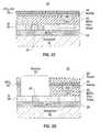
- FIG. 1is a top enlarged view of one non-limiting embodiment of a (symmetrical) NEMS switch that can be constructed using the exemplary embodiments of this invention using a starting SOI wafer.
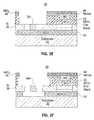
- FIGS. 2A-2Gcollectively referred to as FIG. 2 , show an exemplary process flow in accordance with the exemplary embodiments of this invention, where:
- FIG. 2Aa starting SOI wafer
- FIG. 2Bshows the structure of FIG. 2A after deposition of transistor metal, a back end of line (BEOL) film stack and an overlying layer of nitride;
- BEOLback end of line
- FIG. 2Cshows the structure of FIG. 2B after deposition of a hardmask (HM) layer
- FIG. 2Dshows the structure of FIG. 2C after deposition of a layer of photoresist 48 , the patterning of the photoresist to define a NEMS window, and the selective etching of the underlying materials down to a delineated portion of a NEMS structure;
- FIG. 2Eshows the structure of FIG. 2D after the layer of photoresist is stripped
- FIG. 2Fshows the structure of FIG. 2E after a vapor HF etch process that releases the NEMS structure
- FIG. 2Gshows the structure of FIG. 2F after the HM layer is removed.
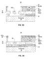
- FIGS. 3A-3Ecollectively referred to as FIG. 3 , show a process flow variation further in accordance with the exemplary embodiments of this invention, where:
- FIG. 3Ais comparable to the structure shown in FIG. 2E ;
- FIG. 3Bshows the structure of FIG. 3A after a nitride layer has been blanket deposited
- FIG. 3Cshows the structure of FIG. 3B after a nitride RIE process that leaves a nitride sleeve or spacer that lines vertical sidewalls of an opened NEMS window;
- FIG. 3Dshows the structure of FIG. 3C after the vapor HF etch process, where the nitride spacer inhibits undercutting of the BEOL film stack
- FIG. 3Eshows the structure of FIG. 3D after the HM layer is removed.
- NEMSand MEMS
- switches in memory and other applicationscan be beneficial.
- electro-mechanical switchescan reduce standby leakage current and potentially can exhibit improved sub-threshold behavior.
- the large control gate voltagetypically some tens volts
- overall reliabilityare two issues that need to be addressed in order to use NEMS as switches.
- a silicon-on-insulator (SOI) substratecan be used for NEMS applications.
- CMOScomplementary metal oxide semiconductor
- NEMS technologiescan be achieved using SOI wafers.
- NEMS/MEMS CMOS co-integrationThere is increased interest in NEMS/MEMS CMOS co-integration to deliver increased functionality and reduced power consumption and/or to provide electrical readout for NEMS/MEMS.
- SOI NEMS/MEMSexhibit good mechanical properties.
- SOI NEMS/MEMS deviceshave found wide application as sensors and transducers.
- SOI-based transistorsare a mainstream manufacturing technology (e.g., partially depleted SOI or PDSOI) and show promise for next generation CMOS scaling (FinFET/Trigate and extremely thin SOI (ETSOI)).
- SOI NEMS/MEMS and SOI FinFET/Trigate transistorscan be integrated monolithically.
- NEMS/MEMS fabricationAn important step in NEMS/MEMS fabrication is structure release, whereby a moveable portion of the NEMS/MEMS device is physically released from the surrounding silicon material and the underlying layer of oxide (buried oxide or BOX) over which it has been photolithographically defined.
- oxideburied oxide or BOX
- NEMS/MEMS structuresThere are certain issues associated with fabricating NEMS/MEMS structures.
- a conventional wet chemical etche.g., one based on hydrofluoric (HF) acid.
- HFhydrofluoric
- Stictionmay be generally defined as a force required to cause one body that is in contact with another body to begin to move.
- Vapor HFis one known technique to release a MEMS/NEMS structure formed on a sacrificial layer of SiO 2 .
- HF vaporWhen HF vapor is employed important requirements for a mask to be used for NEMS/MEMS release, especially when co-integrated with CMOS devices, include a requirement that the mask be resistant to the HF vapor, and that the mask can subsequently be easily removed by a reactive ion etch (RIE) or by dry processing. Ideally the mask removal process should not attack or degrade any already present Si/silicide/metals such as Cu and/or W/nitride.
- RIEreactive ion etch
- the exemplary embodiments of this inventionprovide a process flow that uses HfO 2 as a hard mask for MEMS/NEMS HF vapor release.
- a layer of HfO 2is deposited over a structure containing a NEMS/MEMS that is to be released.
- An openingis formed in the layer of HfO 2 using photolithography and RIE.
- the layer of HfO 2serves as hard mask during NEMS/MEMS release, as even a very thin layer ( ⁇ 2 nm) of HfO 2 is very resistant to HF and oxide RIE chemistries.
- the HfO 2 layeris then subsequently removed by, for example, an RIE process after the NEMS/MEMS structure is released by the use of, for example, a dry, vapor HF process to mitigate stiction and other issues.
- the HfO 2 hard mask-based process flowcan be integrated with a protective spacer (e.g., a spacer formed from a nitride such as Si 3 N 4 ) to prevent an aggressive undercutting of back end of line (BEOL) dielectrics during the HF mediated release process.
- a protective spacere.g., a spacer formed from a nitride such as Si 3 N 4
- teachings of this inventionare not limited to the fabrication of NEMS devices per se, but can be applied as well to the fabrication of MEMS devices and, in general, to the fabrication of a variety of miniaturized electrical-mechanical systems and devices.
- embodimentscan be applied to both SOI and ETSOI starting wafers.
- embodiments of this inventioncan be practiced using an extremely thin SOI (ETSOI) wafer, where the BOX layer may have a thickness of about 50 nm or less and where the overlying layer of Si may have a thickness of about 10 nm or less.
- ESOIextremely thin SOI
- FIG. 1is a top enlarged view of one exemplary and non-limiting embodiment of a (symmetrical) NEMS switch 10 that could be constructed using the exemplary embodiments of this invention using a SOI wafer.
- the structure shownmay be formed to have a total area of less than 5 ⁇ m 2 .
- the switch 10includes an input terminal 12 , an output terminal 14 and control electrodes or terminals 16 and 18 (designated Vdd and GND, respectively.)
- the application of a suitable control input to the terminals 16 and 18results in flexure (motion) of a moveable at least partially electrically conductive structure 20 between a not actuated state and an actuated state.
- the switchWhen in the actuated state (the switch is turned on) an electrically conductive path is established between the input terminal 12 and the output terminal 14 via the electrically conductive portion of the structure 20 that physically contacts the input terminal 12 and the output terminal 14 .
- FIGS. 2A-2Gshow an exemplary process flow in accordance with certain embodiments of this invention.
- FIGS. 3A-3Eshow another exemplary process flow further in accordance with the embodiments of this invention. It can be noted that while a single released member is shown as being formed, in practice a large number of such released members can be simultaneously foamed.
- FIGS. 2A-2GThe embodiment of FIGS. 2A-2G will be described first.
- the SOI wafer 30includes a substrate (e.g., Si) 32 , a layer of buried insulator or buried oxide (BOX) 34 , such as SiO 2 , and an overlying layer of Si 36 .
- the substrate 32can have any suitable thickness.
- the BOX 34can have a thickness in the range of, for example, about 100 nm to about 200 nm, with about 140 nm being one suitable value.
- the Si layer 36can have an initial thickness in the range of, for example, about 50 nm to about 100 nm, with about 80 nm being one suitable value.
- the Si layer 36in which the NEMS structure will be fabricated, has been thinned to a desired thickness in a range of, for example, about 20 nm to about 50 nm, with about 30 nm being one suitable value.
- the Si layer 36is masked and patterned and a reactive ion etch (RIE) process is used to selectively remove a portion of the Si layer 36 to delineate the desired NEMS structure.
- RIEreactive ion etch
- the delineated portionis designated 38 and can correspond to, for example, what will form a part of the moveable electrically conductive structure 20 shown in FIG. 1 .
- This processalso forms what may be referred to as openings or apertures 36 a through the thinned Si layer 36 .
- the delineated portion 38can be considered herein as a “partially released” region of the Si layer 36 , as it is still disposed on the surface of the underlying BOX 34 . This partially released region of the Si layer 36 will be fully released during the performance of the dry etch process described below in reference to FIG. 2F and FIG. 3D .
- FIG. 2Aalso shows an example of a transistor 40 (a CMOS transistor) that has been fabricated in or on the Si layer 36 .
- the stage of processing shown in FIG. 2Amay be considered to be at the completion of a front end of line (FEOL) portion of processing wherein the NEMS and CMOS transistor have been co-integrated.
- the transistor 40can be any type of desired transistor, including a FinFET or a Tri-gate FET.
- FIG. 2Bshows the structure of FIG. 2A after deposition of transistor metal (e.g., metal 1 (M 1 ) and metal 2 (M 2 )), a back end of line (BEOL) film stack 42 (oxide, nitride) and an overlying layer of nitride (e.g., Si 3 N 4 ).
- the M 1can be any desired contact area (CA) metal such as tungsten and can have an exemplary thickness in the range of about 700-800 ⁇ , while the M 2 could be thicker and be composed of, for example, copper or tungsten.
- CAcontact area
- FIG. 2Cshows the structure of FIG. 2B after deposition of a hardmask (HM) layer 46 , preferably one composed of HfO 2 .
- the HfO 2 HM layer 46can have a thickness in a range of about 1-5 nm, with about 2-3 nm being more preferred.
- the HfO 2 HM layer 46can be deposited using atomic layer deposition (ALD) and preferably exhibits a high quality, substantially defect free surface.
- ALDatomic layer deposition
- the use of ALD to deposit HfO 2is well characterized in the art.
- FIG. 2Dshows the structure of FIG. 2C after deposition of a layer of photoresist 48 , the patterning of the photoresist 48 to define a NEMS window 50 , and the selective etching of the underlying HfO 2 HM layer 46 , the nitride layer 44 and the BEOL film stack down to the delineated portion of the NEMS structure 38 to form the NEMS window 50 .
- the selective etchingis preferably a multi-step RIE process where the HfO 2 HM layer 46 is removed with a 250° C. chuck temperature using BCl 3 /Ar at a 5:1 ratio.
- the oxide/nitride RIEcan use CF x with Ar or O 2 .
- FIG. 2Eshows the structure of FIG. 2D after the layer of photoresist 48 is stripped thereby exposing the upper surface of the underlying HfO 2 HM layer 46 .
- FIG. 2Fshows the structure of FIG. 2E after a dry etch, more specifically a vapor HF etch process, is performed to completely remove through the NEMS window 50 remaining portion of the BEOL film stack 42 adjacent to the delineated portion 38 of the Si layer 36 and the underlying material of the BOX 34 , thereby forming a cavity within the BOX material and releasing the delineated portion 38 from the BOX layer 34 to form a released structure 38 A.
- a region of connection between the released structure 38 A and the Si layer 36is not shown.
- the result of the isotropic vapor HF etch processalso serves to undercut to some distance the material of the BOX layer 34 beneath the Si layer 36 as well as to undercut the BEOL film stack 42 beneath the nitride layer 44 . Due to the difference in growth temperatures the BEOL film stack 42 can be undercut to a greater extent than the BOX 34 .
- the HfO 2 HM layer 46is resistant to the vapor HF etch, thereby protecting the underlying material layers.
- FIG. 2Gshows the structure of FIG. 2F after the HfO 2 HM layer 46 is removed.
- the removal processcan include a first step of damaging/degrading the surface of the HfO 2 HM layer 46 followed by RIE using the same chemistry as in FIG. 2D , i.e., a 250° C. chuck temperature using BCl 3 /Ar at a 5:1 ratio.
- the surface of the HfO 2 HM layer 46can be damaged using, for example, a high energy Ar bombardment. This enables the HfO 2 HM layer 46 to be quickly removed by the RIE process with minimal impact of the other structures.
- FIG. 2Gcan be further processed as desired, such as by siliciding at least a portion of the released structure 38 A as described in commonly owned U.S. patent application Ser. No. 13/164,126, filed 20 Jun. 2011, entitled “Silicide Micromechanical Device and Methods to Fabricate Same”, by Michael A. Guillorn, Eric A. Joseph, Fei Liu and Then Zhang.
- FIGS. 3A-3Eshow another exemplary process flow further in accordance with embodiments of this invention, specifically the use of a nitride spacer to prevent the undercutting of the BEOL film stack 42 during the HF etch step.
- FIG. 3Ais comparable to the structure shown in FIG. 2E , i.e., the structure of FIG. 2D after the NEMS window 50 has been opened and the layer of photoresist 48 has stripped thereby exposing the upper surface of the underlying HfO 2 HM layer 46 .
- FIG. 3Bshows the structure of FIG. 3A after a nitride layer 60 has been blanket deposited.
- the nitride layere.g., Si 3 N 4
- the nitride layercan have a thickness in a range of several nanometers to several tens of nanometers and covers the top surface of the HfO 2 HM layer 46 and the sidewalls and bottom surface of the opened NEMS window 50 .
- FIG. 3Cshows the structure of FIG. 3B after a conventional nitride RIE process that serves to remove the nitride from horizontal surfaces, leaving a nitride sleeve or spacer 62 that lines the vertical sidewalls of the opened NEMS window 50 .
- FIG. 3Dshows the structure of FIG. 3C after the dry etch is performed, more specifically the vapor HF etch process.
- the vapor HF etchcompletely removes through the NEMS window 50 remaining portion of the BEOL film stack 42 adjacent to the delineated portion 38 of the Si layer 36 and the underlying material of the BOX 34 , thereby forming the cavity within the BOX material and releasing the delineated portion 38 from the BOX layer 34 to form the released structure 38 A.
- the result of the isotropic vapor HF etch processalso serves to undercut to some distance the material of the BOX layer 34 beneath the Si layer 36 . However, due to the presence of the nitride spacer 62 the undercutting of the BEOL film stack 42 is avoided.
- FIG. 3Eshows the structure of FIG. 3D after the HfO 2 HM layer 46 is removed.
- the removal processcan be performed as described above for FIG. 2G .
- aspects of the present inventionmay be embodied as a system, method or computer program product for controlling the processing of the SOI wafer as discussed above in FIGS. 2 and 3 .
- aspects of the present inventionmay take the form of a computer program product embodied in one or more computer readable medium(s) having computer readable program code embodied thereon. Any combination of one or more computer readable medium(s) may be utilized.
- the computer readable mediummay be a computer readable signal medium or a computer readable storage medium.
- a computer readable storage mediummay be, for example, but not limited to, an electronic, magnetic, optical, electromagnetic, infrared, or semiconductor system, apparatus, or device, or any suitable combination of the foregoing.
- a computer readable storage mediummay be any tangible medium that can contain, or store a program for use by or in connection with an instruction execution system, apparatus, or device.
Landscapes
- Engineering & Computer Science (AREA)
- Manufacturing & Machinery (AREA)
- Microelectronics & Electronic Packaging (AREA)
- Drying Of Semiconductors (AREA)
- Micromachines (AREA)
Abstract
Description
Claims (16)
Priority Applications (3)
| Application Number | Priority Date | Filing Date | Title |
|---|---|---|---|
| US13/313,163US8440523B1 (en) | 2011-12-07 | 2011-12-07 | Micromechanical device and methods to fabricate same using hard mask resistant to structure release etch |
| US13/624,307US9000494B2 (en) | 2011-12-07 | 2012-09-21 | Micromechanical device and methods to fabricate same using hard mask resistant to structure release etch |
| GB1221060.5AGB2497399B (en) | 2011-12-07 | 2012-11-23 | Micromechanical device |
Applications Claiming Priority (1)
| Application Number | Priority Date | Filing Date | Title |
|---|---|---|---|
| US13/313,163US8440523B1 (en) | 2011-12-07 | 2011-12-07 | Micromechanical device and methods to fabricate same using hard mask resistant to structure release etch |
Related Child Applications (1)
| Application Number | Title | Priority Date | Filing Date |
|---|---|---|---|
| US13/624,307ContinuationUS9000494B2 (en) | 2011-12-07 | 2012-09-21 | Micromechanical device and methods to fabricate same using hard mask resistant to structure release etch |
Publications (1)
| Publication Number | Publication Date |
|---|---|
| US8440523B1true US8440523B1 (en) | 2013-05-14 |
Family
ID=47560525
Family Applications (2)
| Application Number | Title | Priority Date | Filing Date |
|---|---|---|---|
| US13/313,163ActiveUS8440523B1 (en) | 2011-12-07 | 2011-12-07 | Micromechanical device and methods to fabricate same using hard mask resistant to structure release etch |
| US13/624,307Expired - Fee RelatedUS9000494B2 (en) | 2011-12-07 | 2012-09-21 | Micromechanical device and methods to fabricate same using hard mask resistant to structure release etch |
Family Applications After (1)
| Application Number | Title | Priority Date | Filing Date |
|---|---|---|---|
| US13/624,307Expired - Fee RelatedUS9000494B2 (en) | 2011-12-07 | 2012-09-21 | Micromechanical device and methods to fabricate same using hard mask resistant to structure release etch |
Country Status (2)
| Country | Link |
|---|---|
| US (2) | US8440523B1 (en) |
| GB (1) | GB2497399B (en) |
Cited By (100)
| Publication number | Priority date | Publication date | Assignee | Title |
|---|---|---|---|---|
| US20130328109A1 (en)* | 2010-12-01 | 2013-12-12 | Cornell University | Structures and methods for electrically and mechanically linked monolithically integrated transistor and mems/nems devices |
| US9721789B1 (en)* | 2016-10-04 | 2017-08-01 | Applied Materials, Inc. | Saving ion-damaged spacers |
| US9741593B2 (en) | 2015-08-06 | 2017-08-22 | Applied Materials, Inc. | Thermal management systems and methods for wafer processing systems |
| US9754800B2 (en) | 2010-05-27 | 2017-09-05 | Applied Materials, Inc. | Selective etch for silicon films |
| US20170261544A1 (en)* | 2016-03-09 | 2017-09-14 | Xallent, LLC | Functional Prober Chip |
| US9768034B1 (en) | 2016-11-11 | 2017-09-19 | Applied Materials, Inc. | Removal methods for high aspect ratio structures |
| US9773648B2 (en) | 2013-08-30 | 2017-09-26 | Applied Materials, Inc. | Dual discharge modes operation for remote plasma |
| US9773695B2 (en) | 2014-07-31 | 2017-09-26 | Applied Materials, Inc. | Integrated bit-line airgap formation and gate stack post clean |
| US9837284B2 (en) | 2014-09-25 | 2017-12-05 | Applied Materials, Inc. | Oxide etch selectivity enhancement |
| US9837249B2 (en) | 2014-03-20 | 2017-12-05 | Applied Materials, Inc. | Radial waveguide systems and methods for post-match control of microwaves |
| US9842744B2 (en) | 2011-03-14 | 2017-12-12 | Applied Materials, Inc. | Methods for etch of SiN films |
| US9865484B1 (en) | 2016-06-29 | 2018-01-09 | Applied Materials, Inc. | Selective etch using material modification and RF pulsing |
| US9881805B2 (en) | 2015-03-02 | 2018-01-30 | Applied Materials, Inc. | Silicon selective removal |
| US9885117B2 (en) | 2014-03-31 | 2018-02-06 | Applied Materials, Inc. | Conditioned semiconductor system parts |
| US9934942B1 (en) | 2016-10-04 | 2018-04-03 | Applied Materials, Inc. | Chamber with flow-through source |
| US9947549B1 (en) | 2016-10-10 | 2018-04-17 | Applied Materials, Inc. | Cobalt-containing material removal |
| US9966240B2 (en) | 2014-10-14 | 2018-05-08 | Applied Materials, Inc. | Systems and methods for internal surface conditioning assessment in plasma processing equipment |
| US9978564B2 (en) | 2012-09-21 | 2018-05-22 | Applied Materials, Inc. | Chemical control features in wafer process equipment |
| US10026621B2 (en) | 2016-11-14 | 2018-07-17 | Applied Materials, Inc. | SiN spacer profile patterning |
| US10032606B2 (en) | 2012-08-02 | 2018-07-24 | Applied Materials, Inc. | Semiconductor processing with DC assisted RF power for improved control |
| US10043684B1 (en) | 2017-02-06 | 2018-08-07 | Applied Materials, Inc. | Self-limiting atomic thermal etching systems and methods |
| US10043674B1 (en) | 2017-08-04 | 2018-08-07 | Applied Materials, Inc. | Germanium etching systems and methods |
| US10049891B1 (en) | 2017-05-31 | 2018-08-14 | Applied Materials, Inc. | Selective in situ cobalt residue removal |
| US10062578B2 (en) | 2011-03-14 | 2018-08-28 | Applied Materials, Inc. | Methods for etch of metal and metal-oxide films |
| US10062575B2 (en) | 2016-09-09 | 2018-08-28 | Applied Materials, Inc. | Poly directional etch by oxidation |
| US10062585B2 (en) | 2016-10-04 | 2018-08-28 | Applied Materials, Inc. | Oxygen compatible plasma source |
| US10062587B2 (en) | 2012-07-18 | 2018-08-28 | Applied Materials, Inc. | Pedestal with multi-zone temperature control and multiple purge capabilities |
| US10062579B2 (en) | 2016-10-07 | 2018-08-28 | Applied Materials, Inc. | Selective SiN lateral recess |
| WO2018187525A1 (en)* | 2017-04-06 | 2018-10-11 | Kwame Amponsah | Nanoelectromechanical devices with metal-to-metal contacts |
| US10128086B1 (en) | 2017-10-24 | 2018-11-13 | Applied Materials, Inc. | Silicon pretreatment for nitride removal |
| US10147620B2 (en) | 2015-08-06 | 2018-12-04 | Applied Materials, Inc. | Bolted wafer chuck thermal management systems and methods for wafer processing systems |
| US10163696B2 (en) | 2016-11-11 | 2018-12-25 | Applied Materials, Inc. | Selective cobalt removal for bottom up gapfill |
| US10170336B1 (en) | 2017-08-04 | 2019-01-01 | Applied Materials, Inc. | Methods for anisotropic control of selective silicon removal |
| US10224210B2 (en) | 2014-12-09 | 2019-03-05 | Applied Materials, Inc. | Plasma processing system with direct outlet toroidal plasma source |
| US10242908B2 (en) | 2016-11-14 | 2019-03-26 | Applied Materials, Inc. | Airgap formation with damage-free copper |
| US10256112B1 (en) | 2017-12-08 | 2019-04-09 | Applied Materials, Inc. | Selective tungsten removal |
| US10256079B2 (en) | 2013-02-08 | 2019-04-09 | Applied Materials, Inc. | Semiconductor processing systems having multiple plasma configurations |
| US10283321B2 (en) | 2011-01-18 | 2019-05-07 | Applied Materials, Inc. | Semiconductor processing system and methods using capacitively coupled plasma |
| US10283324B1 (en) | 2017-10-24 | 2019-05-07 | Applied Materials, Inc. | Oxygen treatment for nitride etching |
| US10297458B2 (en) | 2017-08-07 | 2019-05-21 | Applied Materials, Inc. | Process window widening using coated parts in plasma etch processes |
| US10319649B2 (en) | 2017-04-11 | 2019-06-11 | Applied Materials, Inc. | Optical emission spectroscopy (OES) for remote plasma monitoring |
| US10319600B1 (en) | 2018-03-12 | 2019-06-11 | Applied Materials, Inc. | Thermal silicon etch |
| US10319739B2 (en) | 2017-02-08 | 2019-06-11 | Applied Materials, Inc. | Accommodating imperfectly aligned memory holes |
| US10354889B2 (en) | 2017-07-17 | 2019-07-16 | Applied Materials, Inc. | Non-halogen etching of silicon-containing materials |
| US10403507B2 (en) | 2017-02-03 | 2019-09-03 | Applied Materials, Inc. | Shaped etch profile with oxidation |
| US10424463B2 (en) | 2015-08-07 | 2019-09-24 | Applied Materials, Inc. | Oxide etch selectivity systems and methods |
| US10424485B2 (en) | 2013-03-01 | 2019-09-24 | Applied Materials, Inc. | Enhanced etching processes using remote plasma sources |
| US10436814B2 (en) | 2015-02-26 | 2019-10-08 | Xallent, LLC | Systems and methods for manufacturing nano-electro-mechanical-system probes |
| US10465294B2 (en) | 2014-05-28 | 2019-11-05 | Applied Materials, Inc. | Oxide and metal removal |
| US10468285B2 (en) | 2015-02-03 | 2019-11-05 | Applied Materials, Inc. | High temperature chuck for plasma processing systems |
| US10468267B2 (en) | 2017-05-31 | 2019-11-05 | Applied Materials, Inc. | Water-free etching methods |
| US10490406B2 (en) | 2018-04-10 | 2019-11-26 | Appled Materials, Inc. | Systems and methods for material breakthrough |
| US10497573B2 (en) | 2018-03-13 | 2019-12-03 | Applied Materials, Inc. | Selective atomic layer etching of semiconductor materials |
| US10504700B2 (en) | 2015-08-27 | 2019-12-10 | Applied Materials, Inc. | Plasma etching systems and methods with secondary plasma injection |
| US10504754B2 (en) | 2016-05-19 | 2019-12-10 | Applied Materials, Inc. | Systems and methods for improved semiconductor etching and component protection |
| US10522371B2 (en) | 2016-05-19 | 2019-12-31 | Applied Materials, Inc. | Systems and methods for improved semiconductor etching and component protection |
| US10541184B2 (en) | 2017-07-11 | 2020-01-21 | Applied Materials, Inc. | Optical emission spectroscopic techniques for monitoring etching |
| US10541246B2 (en) | 2017-06-26 | 2020-01-21 | Applied Materials, Inc. | 3D flash memory cells which discourage cross-cell electrical tunneling |
| US10546729B2 (en) | 2016-10-04 | 2020-01-28 | Applied Materials, Inc. | Dual-channel showerhead with improved profile |
| US10566206B2 (en) | 2016-12-27 | 2020-02-18 | Applied Materials, Inc. | Systems and methods for anisotropic material breakthrough |
| US10573527B2 (en) | 2018-04-06 | 2020-02-25 | Applied Materials, Inc. | Gas-phase selective etching systems and methods |
| US10573496B2 (en) | 2014-12-09 | 2020-02-25 | Applied Materials, Inc. | Direct outlet toroidal plasma source |
| US10593523B2 (en) | 2014-10-14 | 2020-03-17 | Applied Materials, Inc. | Systems and methods for internal surface conditioning in plasma processing equipment |
| US10593560B2 (en) | 2018-03-01 | 2020-03-17 | Applied Materials, Inc. | Magnetic induction plasma source for semiconductor processes and equipment |
| US10613115B2 (en) | 2015-02-26 | 2020-04-07 | Xallent, LLC | Multiple integrated tips scanning probe microscope |
| US10615047B2 (en) | 2018-02-28 | 2020-04-07 | Applied Materials, Inc. | Systems and methods to form airgaps |
| US10629473B2 (en) | 2016-09-09 | 2020-04-21 | Applied Materials, Inc. | Footing removal for nitride spacer |
| US10663484B2 (en) | 2018-02-14 | 2020-05-26 | Xallent, LLC | Multiple integrated tips scanning probe microscope with pre-alignment components |
| US10672642B2 (en) | 2018-07-24 | 2020-06-02 | Applied Materials, Inc. | Systems and methods for pedestal configuration |
| US10679870B2 (en) | 2018-02-15 | 2020-06-09 | Applied Materials, Inc. | Semiconductor processing chamber multistage mixing apparatus |
| US10699879B2 (en) | 2018-04-17 | 2020-06-30 | Applied Materials, Inc. | Two piece electrode assembly with gap for plasma control |
| US10727080B2 (en) | 2017-07-07 | 2020-07-28 | Applied Materials, Inc. | Tantalum-containing material removal |
| US10755941B2 (en) | 2018-07-06 | 2020-08-25 | Applied Materials, Inc. | Self-limiting selective etching systems and methods |
| US10854426B2 (en) | 2018-01-08 | 2020-12-01 | Applied Materials, Inc. | Metal recess for semiconductor structures |
| US10872778B2 (en) | 2018-07-06 | 2020-12-22 | Applied Materials, Inc. | Systems and methods utilizing solid-phase etchants |
| US10886137B2 (en) | 2018-04-30 | 2021-01-05 | Applied Materials, Inc. | Selective nitride removal |
| US10892198B2 (en) | 2018-09-14 | 2021-01-12 | Applied Materials, Inc. | Systems and methods for improved performance in semiconductor processing |
| US10903054B2 (en) | 2017-12-19 | 2021-01-26 | Applied Materials, Inc. | Multi-zone gas distribution systems and methods |
| US10903052B2 (en) | 2017-02-03 | 2021-01-26 | Applied Materials, Inc. | Systems and methods for radial and azimuthal control of plasma uniformity |
| US10920319B2 (en) | 2019-01-11 | 2021-02-16 | Applied Materials, Inc. | Ceramic showerheads with conductive electrodes |
| US10920320B2 (en) | 2017-06-16 | 2021-02-16 | Applied Materials, Inc. | Plasma health determination in semiconductor substrate processing reactors |
| US10941037B2 (en) | 2019-01-02 | 2021-03-09 | Nxp Usa, Inc. | Structure and methodology for detecting defects during MEMS device production |
| US10943834B2 (en) | 2017-03-13 | 2021-03-09 | Applied Materials, Inc. | Replacement contact process |
| US10964512B2 (en) | 2018-02-15 | 2021-03-30 | Applied Materials, Inc. | Semiconductor processing chamber multistage mixing apparatus and methods |
| US11027969B2 (en)* | 2017-09-25 | 2021-06-08 | Commissariat A L'energie Atomique Et Aux Energies Alternatives | Micro-device having a metal-semiconductor compound layer protected against HF etching and method for making the same |
| US11049755B2 (en) | 2018-09-14 | 2021-06-29 | Applied Materials, Inc. | Semiconductor substrate supports with embedded RF shield |
| US11062887B2 (en) | 2018-09-17 | 2021-07-13 | Applied Materials, Inc. | High temperature RF heater pedestals |
| US11121002B2 (en) | 2018-10-24 | 2021-09-14 | Applied Materials, Inc. | Systems and methods for etching metals and metal derivatives |
| US11148940B2 (en)* | 2017-10-23 | 2021-10-19 | Fraunhofer-Gesellschaft Zur Foerderung Der Angewandten Forschung E.V. | Microelectromechanical component and method for producing same |
| US11239061B2 (en) | 2014-11-26 | 2022-02-01 | Applied Materials, Inc. | Methods and systems to enhance process uniformity |
| US11257693B2 (en) | 2015-01-09 | 2022-02-22 | Applied Materials, Inc. | Methods and systems to improve pedestal temperature control |
| US11276559B2 (en) | 2017-05-17 | 2022-03-15 | Applied Materials, Inc. | Semiconductor processing chamber for multiple precursor flow |
| US11276590B2 (en) | 2017-05-17 | 2022-03-15 | Applied Materials, Inc. | Multi-zone semiconductor substrate supports |
| US11328909B2 (en) | 2017-12-22 | 2022-05-10 | Applied Materials, Inc. | Chamber conditioning and removal processes |
| US11417534B2 (en) | 2018-09-21 | 2022-08-16 | Applied Materials, Inc. | Selective material removal |
| US11437242B2 (en) | 2018-11-27 | 2022-09-06 | Applied Materials, Inc. | Selective removal of silicon-containing materials |
| US11594428B2 (en) | 2015-02-03 | 2023-02-28 | Applied Materials, Inc. | Low temperature chuck for plasma processing systems |
| US11682560B2 (en) | 2018-10-11 | 2023-06-20 | Applied Materials, Inc. | Systems and methods for hafnium-containing film removal |
| US11721527B2 (en) | 2019-01-07 | 2023-08-08 | Applied Materials, Inc. | Processing chamber mixing systems |
| US12340979B2 (en) | 2017-05-17 | 2025-06-24 | Applied Materials, Inc. | Semiconductor processing chamber for improved precursor flow |
Families Citing this family (1)
| Publication number | Priority date | Publication date | Assignee | Title |
|---|---|---|---|---|
| CN107973267B (en)* | 2015-05-15 | 2020-08-21 | 风起科技股份有限公司 | CMOS sensing assembly, CMOS single chip and manufacturing method |
Citations (27)
| Publication number | Priority date | Publication date | Assignee | Title |
|---|---|---|---|---|
| US5629918A (en)* | 1995-01-20 | 1997-05-13 | The Regents Of The University Of California | Electromagnetically actuated micromachined flap |
| US6399516B1 (en)* | 1998-10-30 | 2002-06-04 | Massachusetts Institute Of Technology | Plasma etch techniques for fabricating silicon structures from a substrate |
| US20040129958A1 (en)* | 2002-03-08 | 2004-07-08 | Koh Philip J. | Compact microwave/millimeter wave filter and method of manufacturing and designing thereof |
| US20040157395A1 (en)* | 2002-12-31 | 2004-08-12 | Yoo Seung Jong | Method for fabricating nonvolatile memory device |
| US20050036196A1 (en)* | 2003-08-12 | 2005-02-17 | Terraop Ltd | Bouncing mode operated scanning micro-mirror |
| US20050036269A1 (en)* | 2001-09-07 | 2005-02-17 | Intel Corporation | Vacuum-cavity MEMS resonator |
| US6900134B1 (en)* | 2004-03-18 | 2005-05-31 | Taiwan Semiconductor Manufacturing Co., Ltd. | Method for forming openings in a substrate using bottom antireflective coatings |
| US20060205106A1 (en)* | 2005-02-25 | 2006-09-14 | Hiroshi Fukuda | Integrated micro electro-mechanical system and manufacturing method thereof |
| US7138694B2 (en)* | 2004-03-02 | 2006-11-21 | Analog Devices, Inc. | Single crystal silicon sensor with additional layer and method of producing the same |
| US20080044772A1 (en)* | 2006-08-18 | 2008-02-21 | Guerrero Douglas J | Anti-reflective imaging layer for multiple patterning process |
| US20080174010A1 (en) | 2006-09-27 | 2008-07-24 | Kabushiki Kaisha Toshiba | Mems element fabrication method and mems element |
| US20080248604A1 (en)* | 2007-04-03 | 2008-10-09 | Christenson John C | Post-logic isolation of silicon regions for an integrated sensor |
| US20080261372A1 (en)* | 2005-03-21 | 2008-10-23 | Honeywell International Inc. | Method of manufacturing vibrating micromechanical structures |
| US20090108381A1 (en)* | 2001-12-10 | 2009-04-30 | International Business Machines Corporation | Low temperature bi-CMOS compatible process for MEMS RF resonators and filters |
| US20090179286A1 (en)* | 2008-01-11 | 2009-07-16 | Florian Schoen | MEMS Devices and Methods of Manufacture Thereof |
| US20100181173A1 (en)* | 2009-01-19 | 2010-07-22 | Rodriguez Lorenzo G | Electrostatically actuated non-latching and latching rf-mems switch |
| US20100243414A1 (en)* | 2009-03-27 | 2010-09-30 | International Business Machines Corporation | Horizontal Micro-Electro-Mechanical-System Switch |
| US7825484B2 (en)* | 2005-04-25 | 2010-11-02 | Analog Devices, Inc. | Micromachined microphone and multisensor and method for producing same |
| US20100279234A1 (en) | 2009-04-01 | 2010-11-04 | Taiwan Semiconductor Manufacturing Company, Ltd. | Double patterning method using metallic compound mask layer |
| US20100314258A1 (en)* | 2002-10-29 | 2010-12-16 | Microfabrica Inc. | Electrochemical Fabrication Processes Incorporating Non-Platable Metals and/or Metals that are Difficult to Plate On |
| US20100314668A1 (en)* | 2007-12-04 | 2010-12-16 | COMMISSARIAT a L' ENERGIE ATOMIQUE ET AUX ENG ALT. | Device with integrated circuit and encapsulated n/mems and method for production |
| US20110279201A1 (en)* | 2010-05-13 | 2011-11-17 | Valtion Teknillinen Tutkimuskeskus | Microelectromechanical resonator and a method for producing the same |
| US8143971B2 (en)* | 2008-07-11 | 2012-03-27 | Taiwan Semiconductor Manufacturing Company, Ltd. | MEMS resonator |
| US20120092082A1 (en)* | 2009-06-09 | 2012-04-19 | Commissariat A L'energie Atomique Et Aux Ene Alt | Electromechanical resonator with resonant anchor |
| US20120273966A1 (en)* | 2010-04-15 | 2012-11-01 | International Business Machines Corporation | Integrated circuit interconnect structure |
| US8309386B2 (en)* | 2005-04-25 | 2012-11-13 | Analog Devices, Inc. | Process of forming a microphone using support member |
| US20120318649A1 (en)* | 2011-06-20 | 2012-12-20 | International Business Machines Corporation | Silicide Micromechanical Device and Methods to Fabricate Same |
Family Cites Families (9)
| Publication number | Priority date | Publication date | Assignee | Title |
|---|---|---|---|---|
| AU2002246913A1 (en)* | 2000-11-22 | 2002-08-06 | The Johns Hopkins University | Method for fabricating a semiconductor device |
| US6667246B2 (en)* | 2001-12-04 | 2003-12-23 | Matsushita Electric Industrial Co., Ltd. | Wet-etching method and method for manufacturing semiconductor device |
| EP1682444A2 (en)* | 2003-10-31 | 2006-07-26 | Koninklijke Philips Electronics N.V. | A method of manufacturing an electronic device and electronic device |
| US7238619B2 (en)* | 2005-07-06 | 2007-07-03 | United Microelectronics Corp. | Method for eliminating bridging defect in via first dual damascene process |
| US7902066B2 (en)* | 2006-09-26 | 2011-03-08 | Chartered Semiconductor Manufacturing, Ltd. | Damascene contact structure for integrated circuits |
| US7868403B1 (en)* | 2007-03-01 | 2011-01-11 | Rf Micro Devices, Inc. | Integrated MEMS resonator device |
| JP5305993B2 (en)* | 2008-05-02 | 2013-10-02 | キヤノン株式会社 | Capacitive electromechanical transducer manufacturing method and capacitive electromechanical transducer |
| FR2946636B1 (en)* | 2009-06-15 | 2012-03-23 | Commissariat Energie Atomique | METHOD FOR THE IMPROVED RELEASE OF THE SUSPENDED STRUCTURE OF AN NEMS AND / OR MEMS COMPONENT |
| US8368155B2 (en)* | 2010-08-26 | 2013-02-05 | The Aerospace Corporation | Systems and methods for preparing freestanding films using laser-assisted chemical etch, and freestanding films formed using same |
- 2011
- 2011-12-07USUS13/313,163patent/US8440523B1/enactiveActive
- 2012
- 2012-09-21USUS13/624,307patent/US9000494B2/ennot_activeExpired - Fee Related
- 2012-11-23GBGB1221060.5Apatent/GB2497399B/ennot_activeExpired - Fee Related
Patent Citations (27)
| Publication number | Priority date | Publication date | Assignee | Title |
|---|---|---|---|---|
| US5629918A (en)* | 1995-01-20 | 1997-05-13 | The Regents Of The University Of California | Electromagnetically actuated micromachined flap |
| US6399516B1 (en)* | 1998-10-30 | 2002-06-04 | Massachusetts Institute Of Technology | Plasma etch techniques for fabricating silicon structures from a substrate |
| US20050036269A1 (en)* | 2001-09-07 | 2005-02-17 | Intel Corporation | Vacuum-cavity MEMS resonator |
| US20090108381A1 (en)* | 2001-12-10 | 2009-04-30 | International Business Machines Corporation | Low temperature bi-CMOS compatible process for MEMS RF resonators and filters |
| US20040129958A1 (en)* | 2002-03-08 | 2004-07-08 | Koh Philip J. | Compact microwave/millimeter wave filter and method of manufacturing and designing thereof |
| US20100314258A1 (en)* | 2002-10-29 | 2010-12-16 | Microfabrica Inc. | Electrochemical Fabrication Processes Incorporating Non-Platable Metals and/or Metals that are Difficult to Plate On |
| US20040157395A1 (en)* | 2002-12-31 | 2004-08-12 | Yoo Seung Jong | Method for fabricating nonvolatile memory device |
| US20050036196A1 (en)* | 2003-08-12 | 2005-02-17 | Terraop Ltd | Bouncing mode operated scanning micro-mirror |
| US7138694B2 (en)* | 2004-03-02 | 2006-11-21 | Analog Devices, Inc. | Single crystal silicon sensor with additional layer and method of producing the same |
| US6900134B1 (en)* | 2004-03-18 | 2005-05-31 | Taiwan Semiconductor Manufacturing Co., Ltd. | Method for forming openings in a substrate using bottom antireflective coatings |
| US20060205106A1 (en)* | 2005-02-25 | 2006-09-14 | Hiroshi Fukuda | Integrated micro electro-mechanical system and manufacturing method thereof |
| US20080261372A1 (en)* | 2005-03-21 | 2008-10-23 | Honeywell International Inc. | Method of manufacturing vibrating micromechanical structures |
| US7825484B2 (en)* | 2005-04-25 | 2010-11-02 | Analog Devices, Inc. | Micromachined microphone and multisensor and method for producing same |
| US8309386B2 (en)* | 2005-04-25 | 2012-11-13 | Analog Devices, Inc. | Process of forming a microphone using support member |
| US20080044772A1 (en)* | 2006-08-18 | 2008-02-21 | Guerrero Douglas J | Anti-reflective imaging layer for multiple patterning process |
| US20080174010A1 (en) | 2006-09-27 | 2008-07-24 | Kabushiki Kaisha Toshiba | Mems element fabrication method and mems element |
| US20080248604A1 (en)* | 2007-04-03 | 2008-10-09 | Christenson John C | Post-logic isolation of silicon regions for an integrated sensor |
| US20100314668A1 (en)* | 2007-12-04 | 2010-12-16 | COMMISSARIAT a L' ENERGIE ATOMIQUE ET AUX ENG ALT. | Device with integrated circuit and encapsulated n/mems and method for production |
| US20090179286A1 (en)* | 2008-01-11 | 2009-07-16 | Florian Schoen | MEMS Devices and Methods of Manufacture Thereof |
| US8143971B2 (en)* | 2008-07-11 | 2012-03-27 | Taiwan Semiconductor Manufacturing Company, Ltd. | MEMS resonator |
| US20100181173A1 (en)* | 2009-01-19 | 2010-07-22 | Rodriguez Lorenzo G | Electrostatically actuated non-latching and latching rf-mems switch |
| US20100243414A1 (en)* | 2009-03-27 | 2010-09-30 | International Business Machines Corporation | Horizontal Micro-Electro-Mechanical-System Switch |
| US20100279234A1 (en) | 2009-04-01 | 2010-11-04 | Taiwan Semiconductor Manufacturing Company, Ltd. | Double patterning method using metallic compound mask layer |
| US20120092082A1 (en)* | 2009-06-09 | 2012-04-19 | Commissariat A L'energie Atomique Et Aux Ene Alt | Electromechanical resonator with resonant anchor |
| US20120273966A1 (en)* | 2010-04-15 | 2012-11-01 | International Business Machines Corporation | Integrated circuit interconnect structure |
| US20110279201A1 (en)* | 2010-05-13 | 2011-11-17 | Valtion Teknillinen Tutkimuskeskus | Microelectromechanical resonator and a method for producing the same |
| US20120318649A1 (en)* | 2011-06-20 | 2012-12-20 | International Business Machines Corporation | Silicide Micromechanical Device and Methods to Fabricate Same |
Non-Patent Citations (10)
| Title |
|---|
| Bakke et al., "Etch Stop Materials for Release by Vapor HF Etching", downloaded on Mar. 30, 2011 and available at http://www.idonus.com/txt/products/vpe/publications/Bakke-MME05%20etch%20stop%20materials%20for%/20release%20by%20vapor%20hf%20etching.pdf. |
| Chen et al., "Investigation of Self-Assembled Monolayer Resists for Hafnium Dixoide Atomic Layer Deposition", Chem. Mater. 2005, 17, 536-544. |
| Chen et al., Achieving Area-Selective Atomic Layer Deposition on Patterned Substrates by Selective Service Modification:, Applied Physics Letters 86, 191910 (2005). |
| Gilgunn et al., "Flip-Chip Integrated SOI-CMOS-MEMS Fabrication Technology", downloaded on Mar. 30, 2011 and available at http://www.ece.cmu.edu/~gilgunn/files/gilgunn-HH-2008.pdf. |
| Gilgunn et al., "Flip-Chip Integrated SOI-CMOS-MEMS Fabrication Technology", downloaded on Mar. 30, 2011 and available at http://www.ece.cmu.edu/˜gilgunn/files/gilgunn—HH—2008.pdf. |
| Knez et al., "Synthesis and Surface Engineering of Complex Nanostructures by Atomic Layer Deposition", Advanced Materials, Adv. Mater. 2007, 19, 3425-3438. |
| MEMS-Exchange Org., "Fabricating MEMS and Nanotechnology", downloaded on Mar. 28, 2011 and available at http://www.mems-exchange.org/MEMS/fabrication.html. |
| Mouaziz et al., "Combined Al-Protection and HF-Vapor Release Process for Ultrathin Single Crystal Silicon Cantilevers", Microelectronic Engineering 83 (2006), pp. 1306-1308, also available on line Feb. 28, 2006 at www.sciencedirect.com and www.elsevier.com/locate/mee. |
| Ramstad et al., "CMOS-MEMS Integration", Mar. 27, 2006, downloaded on Mar. 30, 2011 and available at http://folk.uio.no/janera/master-filer/Essay-27-03-2006.pdf. |
| Williams et al., "Etch Rates for Micromaching Processing-Part II", downloaded on Mar. 30, 2011 and available at http://microlab.berkeley.edu/labmanual/chap1/JMEMSEtchRates2%282003%29.pdf. |
Cited By (143)
| Publication number | Priority date | Publication date | Assignee | Title |
|---|---|---|---|---|
| US9754800B2 (en) | 2010-05-27 | 2017-09-05 | Applied Materials, Inc. | Selective etch for silicon films |
| US9159710B2 (en)* | 2010-12-01 | 2015-10-13 | Cornell University | Structures and methods for electrically and mechanically linked monolithically integrated transistor and NEMS/MEMS device |
| US20130328109A1 (en)* | 2010-12-01 | 2013-12-12 | Cornell University | Structures and methods for electrically and mechanically linked monolithically integrated transistor and mems/nems devices |
| US10283321B2 (en) | 2011-01-18 | 2019-05-07 | Applied Materials, Inc. | Semiconductor processing system and methods using capacitively coupled plasma |
| US9842744B2 (en) | 2011-03-14 | 2017-12-12 | Applied Materials, Inc. | Methods for etch of SiN films |
| US10062578B2 (en) | 2011-03-14 | 2018-08-28 | Applied Materials, Inc. | Methods for etch of metal and metal-oxide films |
| US10062587B2 (en) | 2012-07-18 | 2018-08-28 | Applied Materials, Inc. | Pedestal with multi-zone temperature control and multiple purge capabilities |
| US10032606B2 (en) | 2012-08-02 | 2018-07-24 | Applied Materials, Inc. | Semiconductor processing with DC assisted RF power for improved control |
| US11264213B2 (en) | 2012-09-21 | 2022-03-01 | Applied Materials, Inc. | Chemical control features in wafer process equipment |
| US10354843B2 (en) | 2012-09-21 | 2019-07-16 | Applied Materials, Inc. | Chemical control features in wafer process equipment |
| US9978564B2 (en) | 2012-09-21 | 2018-05-22 | Applied Materials, Inc. | Chemical control features in wafer process equipment |
| US11024486B2 (en) | 2013-02-08 | 2021-06-01 | Applied Materials, Inc. | Semiconductor processing systems having multiple plasma configurations |
| US10256079B2 (en) | 2013-02-08 | 2019-04-09 | Applied Materials, Inc. | Semiconductor processing systems having multiple plasma configurations |
| US10424485B2 (en) | 2013-03-01 | 2019-09-24 | Applied Materials, Inc. | Enhanced etching processes using remote plasma sources |
| US9773648B2 (en) | 2013-08-30 | 2017-09-26 | Applied Materials, Inc. | Dual discharge modes operation for remote plasma |
| US9837249B2 (en) | 2014-03-20 | 2017-12-05 | Applied Materials, Inc. | Radial waveguide systems and methods for post-match control of microwaves |
| US9903020B2 (en) | 2014-03-31 | 2018-02-27 | Applied Materials, Inc. | Generation of compact alumina passivation layers on aluminum plasma equipment components |
| US9885117B2 (en) | 2014-03-31 | 2018-02-06 | Applied Materials, Inc. | Conditioned semiconductor system parts |
| US10465294B2 (en) | 2014-05-28 | 2019-11-05 | Applied Materials, Inc. | Oxide and metal removal |
| US9773695B2 (en) | 2014-07-31 | 2017-09-26 | Applied Materials, Inc. | Integrated bit-line airgap formation and gate stack post clean |
| US9837284B2 (en) | 2014-09-25 | 2017-12-05 | Applied Materials, Inc. | Oxide etch selectivity enhancement |
| US10707061B2 (en) | 2014-10-14 | 2020-07-07 | Applied Materials, Inc. | Systems and methods for internal surface conditioning in plasma processing equipment |
| US10796922B2 (en) | 2014-10-14 | 2020-10-06 | Applied Materials, Inc. | Systems and methods for internal surface conditioning assessment in plasma processing equipment |
| US9966240B2 (en) | 2014-10-14 | 2018-05-08 | Applied Materials, Inc. | Systems and methods for internal surface conditioning assessment in plasma processing equipment |
| US10490418B2 (en) | 2014-10-14 | 2019-11-26 | Applied Materials, Inc. | Systems and methods for internal surface conditioning assessment in plasma processing equipment |
| US10593523B2 (en) | 2014-10-14 | 2020-03-17 | Applied Materials, Inc. | Systems and methods for internal surface conditioning in plasma processing equipment |
| US11637002B2 (en) | 2014-11-26 | 2023-04-25 | Applied Materials, Inc. | Methods and systems to enhance process uniformity |
| US11239061B2 (en) | 2014-11-26 | 2022-02-01 | Applied Materials, Inc. | Methods and systems to enhance process uniformity |
| US10224210B2 (en) | 2014-12-09 | 2019-03-05 | Applied Materials, Inc. | Plasma processing system with direct outlet toroidal plasma source |
| US10573496B2 (en) | 2014-12-09 | 2020-02-25 | Applied Materials, Inc. | Direct outlet toroidal plasma source |
| US11257693B2 (en) | 2015-01-09 | 2022-02-22 | Applied Materials, Inc. | Methods and systems to improve pedestal temperature control |
| US11594428B2 (en) | 2015-02-03 | 2023-02-28 | Applied Materials, Inc. | Low temperature chuck for plasma processing systems |
| US12009228B2 (en) | 2015-02-03 | 2024-06-11 | Applied Materials, Inc. | Low temperature chuck for plasma processing systems |
| US10468285B2 (en) | 2015-02-03 | 2019-11-05 | Applied Materials, Inc. | High temperature chuck for plasma processing systems |
| US11573247B2 (en) | 2015-02-26 | 2023-02-07 | Xallent Inc. | Systems and methods for manufacturing nano-electro-mechanical-system probes |
| US11125774B2 (en) | 2015-02-26 | 2021-09-21 | Xallent Llc | Systems and methods for manufacturing nano-electro-mechanical-system probes |
| US10436814B2 (en) | 2015-02-26 | 2019-10-08 | Xallent, LLC | Systems and methods for manufacturing nano-electro-mechanical-system probes |
| US10545171B2 (en) | 2015-02-26 | 2020-01-28 | Xallent, LLC | Systems and methods for manufacturing nano-electro-mechanical-system probes |
| US10895585B2 (en) | 2015-02-26 | 2021-01-19 | Xallent, LLC | Multiple integrated tips scanning probe microscope |
| US10613115B2 (en) | 2015-02-26 | 2020-04-07 | Xallent, LLC | Multiple integrated tips scanning probe microscope |
| US9881805B2 (en) | 2015-03-02 | 2018-01-30 | Applied Materials, Inc. | Silicon selective removal |
| US10468276B2 (en) | 2015-08-06 | 2019-11-05 | Applied Materials, Inc. | Thermal management systems and methods for wafer processing systems |
| US11158527B2 (en) | 2015-08-06 | 2021-10-26 | Applied Materials, Inc. | Thermal management systems and methods for wafer processing systems |
| US9741593B2 (en) | 2015-08-06 | 2017-08-22 | Applied Materials, Inc. | Thermal management systems and methods for wafer processing systems |
| US10607867B2 (en) | 2015-08-06 | 2020-03-31 | Applied Materials, Inc. | Bolted wafer chuck thermal management systems and methods for wafer processing systems |
| US10147620B2 (en) | 2015-08-06 | 2018-12-04 | Applied Materials, Inc. | Bolted wafer chuck thermal management systems and methods for wafer processing systems |
| US10424464B2 (en) | 2015-08-07 | 2019-09-24 | Applied Materials, Inc. | Oxide etch selectivity systems and methods |
| US10424463B2 (en) | 2015-08-07 | 2019-09-24 | Applied Materials, Inc. | Oxide etch selectivity systems and methods |
| US11476093B2 (en) | 2015-08-27 | 2022-10-18 | Applied Materials, Inc. | Plasma etching systems and methods with secondary plasma injection |
| US10504700B2 (en) | 2015-08-27 | 2019-12-10 | Applied Materials, Inc. | Plasma etching systems and methods with secondary plasma injection |
| US20170261544A1 (en)* | 2016-03-09 | 2017-09-14 | Xallent, LLC | Functional Prober Chip |
| US11280825B2 (en) | 2016-03-09 | 2022-03-22 | Xallent Llc | Functional prober chip |
| US10866273B2 (en)* | 2016-03-09 | 2020-12-15 | Xallent, LLC | Functional prober chip |
| US11735441B2 (en) | 2016-05-19 | 2023-08-22 | Applied Materials, Inc. | Systems and methods for improved semiconductor etching and component protection |
| US10522371B2 (en) | 2016-05-19 | 2019-12-31 | Applied Materials, Inc. | Systems and methods for improved semiconductor etching and component protection |
| US10504754B2 (en) | 2016-05-19 | 2019-12-10 | Applied Materials, Inc. | Systems and methods for improved semiconductor etching and component protection |
| US12057329B2 (en) | 2016-06-29 | 2024-08-06 | Applied Materials, Inc. | Selective etch using material modification and RF pulsing |
| US9865484B1 (en) | 2016-06-29 | 2018-01-09 | Applied Materials, Inc. | Selective etch using material modification and RF pulsing |
| US10629473B2 (en) | 2016-09-09 | 2020-04-21 | Applied Materials, Inc. | Footing removal for nitride spacer |
| US10062575B2 (en) | 2016-09-09 | 2018-08-28 | Applied Materials, Inc. | Poly directional etch by oxidation |
| US10062585B2 (en) | 2016-10-04 | 2018-08-28 | Applied Materials, Inc. | Oxygen compatible plasma source |
| US10541113B2 (en) | 2016-10-04 | 2020-01-21 | Applied Materials, Inc. | Chamber with flow-through source |
| US9721789B1 (en)* | 2016-10-04 | 2017-08-01 | Applied Materials, Inc. | Saving ion-damaged spacers |
| US11049698B2 (en) | 2016-10-04 | 2021-06-29 | Applied Materials, Inc. | Dual-channel showerhead with improved profile |
| US10224180B2 (en) | 2016-10-04 | 2019-03-05 | Applied Materials, Inc. | Chamber with flow-through source |
| US9934942B1 (en) | 2016-10-04 | 2018-04-03 | Applied Materials, Inc. | Chamber with flow-through source |
| US10546729B2 (en) | 2016-10-04 | 2020-01-28 | Applied Materials, Inc. | Dual-channel showerhead with improved profile |
| US10319603B2 (en) | 2016-10-07 | 2019-06-11 | Applied Materials, Inc. | Selective SiN lateral recess |
| US10062579B2 (en) | 2016-10-07 | 2018-08-28 | Applied Materials, Inc. | Selective SiN lateral recess |
| US9947549B1 (en) | 2016-10-10 | 2018-04-17 | Applied Materials, Inc. | Cobalt-containing material removal |
| US10186428B2 (en) | 2016-11-11 | 2019-01-22 | Applied Materials, Inc. | Removal methods for high aspect ratio structures |
| US10770346B2 (en) | 2016-11-11 | 2020-09-08 | Applied Materials, Inc. | Selective cobalt removal for bottom up gapfill |
| US10163696B2 (en) | 2016-11-11 | 2018-12-25 | Applied Materials, Inc. | Selective cobalt removal for bottom up gapfill |
| US9768034B1 (en) | 2016-11-11 | 2017-09-19 | Applied Materials, Inc. | Removal methods for high aspect ratio structures |
| US10242908B2 (en) | 2016-11-14 | 2019-03-26 | Applied Materials, Inc. | Airgap formation with damage-free copper |
| US10026621B2 (en) | 2016-11-14 | 2018-07-17 | Applied Materials, Inc. | SiN spacer profile patterning |
| US10600639B2 (en) | 2016-11-14 | 2020-03-24 | Applied Materials, Inc. | SiN spacer profile patterning |
| US10566206B2 (en) | 2016-12-27 | 2020-02-18 | Applied Materials, Inc. | Systems and methods for anisotropic material breakthrough |
| US10903052B2 (en) | 2017-02-03 | 2021-01-26 | Applied Materials, Inc. | Systems and methods for radial and azimuthal control of plasma uniformity |
| US10403507B2 (en) | 2017-02-03 | 2019-09-03 | Applied Materials, Inc. | Shaped etch profile with oxidation |
| US10043684B1 (en) | 2017-02-06 | 2018-08-07 | Applied Materials, Inc. | Self-limiting atomic thermal etching systems and methods |
| US10319739B2 (en) | 2017-02-08 | 2019-06-11 | Applied Materials, Inc. | Accommodating imperfectly aligned memory holes |
| US10529737B2 (en) | 2017-02-08 | 2020-01-07 | Applied Materials, Inc. | Accommodating imperfectly aligned memory holes |
| US10325923B2 (en) | 2017-02-08 | 2019-06-18 | Applied Materials, Inc. | Accommodating imperfectly aligned memory holes |
| US10943834B2 (en) | 2017-03-13 | 2021-03-09 | Applied Materials, Inc. | Replacement contact process |
| WO2018187525A1 (en)* | 2017-04-06 | 2018-10-11 | Kwame Amponsah | Nanoelectromechanical devices with metal-to-metal contacts |
| US11017959B2 (en) | 2017-04-06 | 2021-05-25 | Kwame Amponsah | Nanoelectromechanical devices with metal-to-metal contacts |
| US10784054B2 (en) | 2017-04-06 | 2020-09-22 | Kwame Amponsah | Nanoelectromechanical devices with metal-to-metal contacts |
| US10319649B2 (en) | 2017-04-11 | 2019-06-11 | Applied Materials, Inc. | Optical emission spectroscopy (OES) for remote plasma monitoring |
| US11276590B2 (en) | 2017-05-17 | 2022-03-15 | Applied Materials, Inc. | Multi-zone semiconductor substrate supports |
| US11915950B2 (en) | 2017-05-17 | 2024-02-27 | Applied Materials, Inc. | Multi-zone semiconductor substrate supports |
| US11276559B2 (en) | 2017-05-17 | 2022-03-15 | Applied Materials, Inc. | Semiconductor processing chamber for multiple precursor flow |
| US12340979B2 (en) | 2017-05-17 | 2025-06-24 | Applied Materials, Inc. | Semiconductor processing chamber for improved precursor flow |
| US11361939B2 (en) | 2017-05-17 | 2022-06-14 | Applied Materials, Inc. | Semiconductor processing chamber for multiple precursor flow |
| US10497579B2 (en) | 2017-05-31 | 2019-12-03 | Applied Materials, Inc. | Water-free etching methods |
| US10049891B1 (en) | 2017-05-31 | 2018-08-14 | Applied Materials, Inc. | Selective in situ cobalt residue removal |
| US10468267B2 (en) | 2017-05-31 | 2019-11-05 | Applied Materials, Inc. | Water-free etching methods |
| US10920320B2 (en) | 2017-06-16 | 2021-02-16 | Applied Materials, Inc. | Plasma health determination in semiconductor substrate processing reactors |
| US10541246B2 (en) | 2017-06-26 | 2020-01-21 | Applied Materials, Inc. | 3D flash memory cells which discourage cross-cell electrical tunneling |
| US10727080B2 (en) | 2017-07-07 | 2020-07-28 | Applied Materials, Inc. | Tantalum-containing material removal |
| US10541184B2 (en) | 2017-07-11 | 2020-01-21 | Applied Materials, Inc. | Optical emission spectroscopic techniques for monitoring etching |
| US10354889B2 (en) | 2017-07-17 | 2019-07-16 | Applied Materials, Inc. | Non-halogen etching of silicon-containing materials |
| US10593553B2 (en) | 2017-08-04 | 2020-03-17 | Applied Materials, Inc. | Germanium etching systems and methods |
| US10043674B1 (en) | 2017-08-04 | 2018-08-07 | Applied Materials, Inc. | Germanium etching systems and methods |
| US10170336B1 (en) | 2017-08-04 | 2019-01-01 | Applied Materials, Inc. | Methods for anisotropic control of selective silicon removal |
| US10297458B2 (en) | 2017-08-07 | 2019-05-21 | Applied Materials, Inc. | Process window widening using coated parts in plasma etch processes |
| US11101136B2 (en) | 2017-08-07 | 2021-08-24 | Applied Materials, Inc. | Process window widening using coated parts in plasma etch processes |
| US11027969B2 (en)* | 2017-09-25 | 2021-06-08 | Commissariat A L'energie Atomique Et Aux Energies Alternatives | Micro-device having a metal-semiconductor compound layer protected against HF etching and method for making the same |
| US11148940B2 (en)* | 2017-10-23 | 2021-10-19 | Fraunhofer-Gesellschaft Zur Foerderung Der Angewandten Forschung E.V. | Microelectromechanical component and method for producing same |
| US10283324B1 (en) | 2017-10-24 | 2019-05-07 | Applied Materials, Inc. | Oxygen treatment for nitride etching |
| US10128086B1 (en) | 2017-10-24 | 2018-11-13 | Applied Materials, Inc. | Silicon pretreatment for nitride removal |
| US10256112B1 (en) | 2017-12-08 | 2019-04-09 | Applied Materials, Inc. | Selective tungsten removal |
| US10903054B2 (en) | 2017-12-19 | 2021-01-26 | Applied Materials, Inc. | Multi-zone gas distribution systems and methods |
| US12148597B2 (en) | 2017-12-19 | 2024-11-19 | Applied Materials, Inc. | Multi-zone gas distribution systems and methods |
| US11328909B2 (en) | 2017-12-22 | 2022-05-10 | Applied Materials, Inc. | Chamber conditioning and removal processes |
| US10854426B2 (en) | 2018-01-08 | 2020-12-01 | Applied Materials, Inc. | Metal recess for semiconductor structures |
| US10861676B2 (en) | 2018-01-08 | 2020-12-08 | Applied Materials, Inc. | Metal recess for semiconductor structures |
| US10663484B2 (en) | 2018-02-14 | 2020-05-26 | Xallent, LLC | Multiple integrated tips scanning probe microscope with pre-alignment components |
| US10679870B2 (en) | 2018-02-15 | 2020-06-09 | Applied Materials, Inc. | Semiconductor processing chamber multistage mixing apparatus |
| US10699921B2 (en) | 2018-02-15 | 2020-06-30 | Applied Materials, Inc. | Semiconductor processing chamber multistage mixing apparatus |
| US10964512B2 (en) | 2018-02-15 | 2021-03-30 | Applied Materials, Inc. | Semiconductor processing chamber multistage mixing apparatus and methods |
| US10615047B2 (en) | 2018-02-28 | 2020-04-07 | Applied Materials, Inc. | Systems and methods to form airgaps |
| US10593560B2 (en) | 2018-03-01 | 2020-03-17 | Applied Materials, Inc. | Magnetic induction plasma source for semiconductor processes and equipment |
| US11004689B2 (en) | 2018-03-12 | 2021-05-11 | Applied Materials, Inc. | Thermal silicon etch |
| US10319600B1 (en) | 2018-03-12 | 2019-06-11 | Applied Materials, Inc. | Thermal silicon etch |
| US10497573B2 (en) | 2018-03-13 | 2019-12-03 | Applied Materials, Inc. | Selective atomic layer etching of semiconductor materials |
| US10573527B2 (en) | 2018-04-06 | 2020-02-25 | Applied Materials, Inc. | Gas-phase selective etching systems and methods |
| US10490406B2 (en) | 2018-04-10 | 2019-11-26 | Appled Materials, Inc. | Systems and methods for material breakthrough |
| US10699879B2 (en) | 2018-04-17 | 2020-06-30 | Applied Materials, Inc. | Two piece electrode assembly with gap for plasma control |
| US10886137B2 (en) | 2018-04-30 | 2021-01-05 | Applied Materials, Inc. | Selective nitride removal |
| US10755941B2 (en) | 2018-07-06 | 2020-08-25 | Applied Materials, Inc. | Self-limiting selective etching systems and methods |
| US10872778B2 (en) | 2018-07-06 | 2020-12-22 | Applied Materials, Inc. | Systems and methods utilizing solid-phase etchants |
| US10672642B2 (en) | 2018-07-24 | 2020-06-02 | Applied Materials, Inc. | Systems and methods for pedestal configuration |
| US10892198B2 (en) | 2018-09-14 | 2021-01-12 | Applied Materials, Inc. | Systems and methods for improved performance in semiconductor processing |
| US11049755B2 (en) | 2018-09-14 | 2021-06-29 | Applied Materials, Inc. | Semiconductor substrate supports with embedded RF shield |
| US11062887B2 (en) | 2018-09-17 | 2021-07-13 | Applied Materials, Inc. | High temperature RF heater pedestals |
| US11417534B2 (en) | 2018-09-21 | 2022-08-16 | Applied Materials, Inc. | Selective material removal |
| US11682560B2 (en) | 2018-10-11 | 2023-06-20 | Applied Materials, Inc. | Systems and methods for hafnium-containing film removal |
| US11121002B2 (en) | 2018-10-24 | 2021-09-14 | Applied Materials, Inc. | Systems and methods for etching metals and metal derivatives |
| US11437242B2 (en) | 2018-11-27 | 2022-09-06 | Applied Materials, Inc. | Selective removal of silicon-containing materials |
| US10941037B2 (en) | 2019-01-02 | 2021-03-09 | Nxp Usa, Inc. | Structure and methodology for detecting defects during MEMS device production |
| US11721527B2 (en) | 2019-01-07 | 2023-08-08 | Applied Materials, Inc. | Processing chamber mixing systems |
| US10920319B2 (en) | 2019-01-11 | 2021-02-16 | Applied Materials, Inc. | Ceramic showerheads with conductive electrodes |
Also Published As
| Publication number | Publication date |
|---|---|
| GB201221060D0 (en) | 2013-01-09 |
| GB2497399A (en) | 2013-06-12 |
| GB2497399B (en) | 2014-02-19 |
| US20130146948A1 (en) | 2013-06-13 |
| US9000494B2 (en) | 2015-04-07 |
Similar Documents
| Publication | Publication Date | Title |
|---|---|---|
| US8440523B1 (en) | Micromechanical device and methods to fabricate same using hard mask resistant to structure release etch | |
| US8993907B2 (en) | Silicide micromechanical device and methods to fabricate same | |
| US6440766B1 (en) | Microfabrication using germanium-based release masks | |
| KR100834829B1 (en) | Multi-bit electromechanical memory device and manufacturing method thereof | |
| US10889493B2 (en) | MEMS method and structure | |
| JP2009043537A (en) | MEMS switch and manufacturing method thereof | |
| WO2007038177A2 (en) | Method for fabricating nanocoils | |
| CN109205548B (en) | Micro-electro-mechanical system (MEMS) device and method of making the same | |
| SG180162A1 (en) | A switching device and a method for forming a switching device | |
| US20090014296A1 (en) | Contact configurations for MEMS relays and MEMS switches and method for making same | |
| JP4804752B2 (en) | Conductive etch stop for etching sacrificial layers | |
| CN102583224B (en) | MEMS (micro-electromechanical system) and IC (integrated circuit) monolithical integration method | |
| US9293687B1 (en) | Passivation and alignment of piezoelectronic transistor piezoresistor | |
| US20150170923A1 (en) | Feature Size Reduction in Semiconductor Devices by Selective Wet Etching | |
| US9162877B2 (en) | Lateral etch stop for NEMS release etch for high density NEMS/CMOS monolithic integration | |
| Lee et al. | Titanium nitride sidewall stringer process for lateral nanoelectromechanical relays | |
| US20080179182A1 (en) | Method for fabricating a Micro-Electromechanical device | |
| US8143158B2 (en) | Method and device of preventing delamination of semiconductor layers | |
| CN103964364B (en) | Micro-nano electrostatic force switch and manufacturing method thereof | |
| US20060281214A1 (en) | Method of making a soi silicon structure | |
| JP2006224219A (en) | Manufacturing method of MEMS element | |
| WO2012177954A2 (en) | Bi-metallic actuators | |
| Lee et al. | Multi-spacer technique for low-voltage, high-aspect-ratio lateral electrostatic actuators | |
| JP2007111831A (en) | Method for manufacturing MEMS element and MEMS element | |
| JPH09162462A (en) | Manufacturing method of semiconductor device having micromachine and electronic circuit |
Legal Events
| Date | Code | Title | Description |
|---|---|---|---|
| AS | Assignment | Owner name:INTERNATIONAL BUSINESS MACHINES CORPORATION, NEW Y Free format text:ASSIGNMENT OF ASSIGNORS INTEREST;ASSIGNORS:GUILLORN, MICHAEL A.;LIU, FEI;ZHANG, YING;SIGNING DATES FROM 20111109 TO 20111130;REEL/FRAME:027339/0521 | |
| STCF | Information on status: patent grant | Free format text:PATENTED CASE | |
| AS | Assignment | Owner name:GLOBALFOUNDRIES U.S. 2 LLC, NEW YORK Free format text:ASSIGNMENT OF ASSIGNORS INTEREST;ASSIGNOR:INTERNATIONAL BUSINESS MACHINES CORPORATION;REEL/FRAME:036550/0001 Effective date:20150629 | |
| AS | Assignment | Owner name:GLOBALFOUNDRIES INC., CAYMAN ISLANDS Free format text:ASSIGNMENT OF ASSIGNORS INTEREST;ASSIGNORS:GLOBALFOUNDRIES U.S. 2 LLC;GLOBALFOUNDRIES U.S. INC.;REEL/FRAME:036779/0001 Effective date:20150910 | |
| FPAY | Fee payment | Year of fee payment:4 | |
| AS | Assignment | Owner name:WILMINGTON TRUST, NATIONAL ASSOCIATION, DELAWARE Free format text:SECURITY AGREEMENT;ASSIGNOR:GLOBALFOUNDRIES INC.;REEL/FRAME:049490/0001 Effective date:20181127 | |
| MAFP | Maintenance fee payment | Free format text:PAYMENT OF MAINTENANCE FEE, 8TH YEAR, LARGE ENTITY (ORIGINAL EVENT CODE: M1552); ENTITY STATUS OF PATENT OWNER: LARGE ENTITY Year of fee payment:8 | |
| AS | Assignment | Owner name:GLOBALFOUNDRIES U.S. INC., CALIFORNIA Free format text:ASSIGNMENT OF ASSIGNORS INTEREST;ASSIGNOR:GLOBALFOUNDRIES INC.;REEL/FRAME:054633/0001 Effective date:20201022 | |
| AS | Assignment | Owner name:GLOBALFOUNDRIES INC., CAYMAN ISLANDS Free format text:RELEASE BY SECURED PARTY;ASSIGNOR:WILMINGTON TRUST, NATIONAL ASSOCIATION;REEL/FRAME:054636/0001 Effective date:20201117 | |
| AS | Assignment | Owner name:GLOBALFOUNDRIES U.S. INC., NEW YORK Free format text:RELEASE BY SECURED PARTY;ASSIGNOR:WILMINGTON TRUST, NATIONAL ASSOCIATION;REEL/FRAME:056987/0001 Effective date:20201117 | |
| MAFP | Maintenance fee payment | Free format text:PAYMENT OF MAINTENANCE FEE, 12TH YEAR, LARGE ENTITY (ORIGINAL EVENT CODE: M1553); ENTITY STATUS OF PATENT OWNER: LARGE ENTITY Year of fee payment:12 |