US8437695B2 - Power bridge circuit for bi-directional inductive signaling - Google Patents
Power bridge circuit for bi-directional inductive signalingDownload PDFInfo
- Publication number
- US8437695B2 US8437695B2US12/841,001US84100110AUS8437695B2US 8437695 B2US8437695 B2US 8437695B2US 84100110 AUS84100110 AUS 84100110AUS 8437695 B2US8437695 B2US 8437695B2
- Authority
- US
- United States
- Prior art keywords
- power
- signal
- mode
- signal interface
- bridge circuit
- Prior art date
- Legal status (The legal status is an assumption and is not a legal conclusion. Google has not performed a legal analysis and makes no representation as to the accuracy of the status listed.)
- Active, expires
Links
- 230000001939inductive effectEffects0.000titleclaimsabstractdescription154
- 230000011664signalingEffects0.000titledescription2
- 238000004891communicationMethods0.000claimsdescription45
- 230000008878couplingEffects0.000claimsdescription11
- 238000010168coupling processMethods0.000claimsdescription11
- 238000005859coupling reactionMethods0.000claimsdescription11
- 230000005540biological transmissionEffects0.000claimsdescription4
- 230000006870functionEffects0.000description16
- 238000010586diagramMethods0.000description15
- 238000006243chemical reactionMethods0.000description14
- 238000012545processingMethods0.000description14
- 238000003032molecular dockingMethods0.000description12
- 238000012546transferMethods0.000description8
- 230000001413cellular effectEffects0.000description3
- 239000004020conductorSubstances0.000description3
- 238000000034methodMethods0.000description3
- 230000004044responseEffects0.000description3
- 230000009471actionEffects0.000description2
- 230000008901benefitEffects0.000description2
- 238000001514detection methodMethods0.000description2
- 230000014759maintenance of locationEffects0.000description2
- 230000008569processEffects0.000description2
- CWYNVVGOOAEACU-UHFFFAOYSA-NFe2+Chemical compound[Fe+2]CWYNVVGOOAEACU-UHFFFAOYSA-N0.000description1
- 241001071864Lethrinus laticaudisSpecies0.000description1
- 230000006399behaviorEffects0.000description1
- 230000005669field effectEffects0.000description1
- 239000000463materialSubstances0.000description1
- 230000005055memory storageEffects0.000description1
- 229910044991metal oxideInorganic materials0.000description1
- 150000004706metal oxidesChemical class0.000description1
- 238000012986modificationMethods0.000description1
- 230000004048modificationEffects0.000description1
- 238000012544monitoring processMethods0.000description1
- 230000003287optical effectEffects0.000description1
- 230000000644propagated effectEffects0.000description1
- 230000001902propagating effectEffects0.000description1
- 230000000717retained effectEffects0.000description1
- 239000004065semiconductorSubstances0.000description1
- 230000001360synchronised effectEffects0.000description1
- 230000001960triggered effectEffects0.000description1
Images


Classifications
- H—ELECTRICITY
- H04—ELECTRIC COMMUNICATION TECHNIQUE
- H04B—TRANSMISSION
- H04B3/00—Line transmission systems
- H04B3/54—Systems for transmission via power distribution lines
- H04B3/548—Systems for transmission via power distribution lines the power on the line being DC
- H—ELECTRICITY
- H02—GENERATION; CONVERSION OR DISTRIBUTION OF ELECTRIC POWER
- H02J—CIRCUIT ARRANGEMENTS OR SYSTEMS FOR SUPPLYING OR DISTRIBUTING ELECTRIC POWER; SYSTEMS FOR STORING ELECTRIC ENERGY
- H02J7/00—Circuit arrangements for charging or depolarising batteries or for supplying loads from batteries
- H02J7/0029—Circuit arrangements for charging or depolarising batteries or for supplying loads from batteries with safety or protection devices or circuits
- H02J7/00308—Overvoltage protection
- H—ELECTRICITY
- H02—GENERATION; CONVERSION OR DISTRIBUTION OF ELECTRIC POWER
- H02J—CIRCUIT ARRANGEMENTS OR SYSTEMS FOR SUPPLYING OR DISTRIBUTING ELECTRIC POWER; SYSTEMS FOR STORING ELECTRIC ENERGY
- H02J50/00—Circuit arrangements or systems for wireless supply or distribution of electric power
- H02J50/10—Circuit arrangements or systems for wireless supply or distribution of electric power using inductive coupling
- H02J50/12—Circuit arrangements or systems for wireless supply or distribution of electric power using inductive coupling of the resonant type
- H—ELECTRICITY
- H04—ELECTRIC COMMUNICATION TECHNIQUE
- H04B—TRANSMISSION
- H04B2203/00—Indexing scheme relating to line transmission systems
- H04B2203/54—Aspects of powerline communications not already covered by H04B3/54 and its subgroups
- H04B2203/5462—Systems for power line communications
- H04B2203/547—Systems for power line communications via DC power distribution
Definitions
- the disclosed embodimentsrelate generally to the field of inductive signal interfaces.
- the disclosed embodimentsrelate to a power bridge circuit for bi-directional inductive signaling.
- FIG. 1Aillustrates a conventional, prior art H-bridge inverter circuit 110 for transferring power from a DC supply 120 to an AC load 115 .
- the H-bridge inverter circuit 110includes four switches 111 - 114 .
- the switches 111 - 114turn on and off in pairs to deliver an AC current to the AC load 115 .
- switches 111 and 114are turned on, while the switches 112 and 113 are turned off.
- switches 111 and 114are turned off, switches 112 and 113 are turned on.
- the currentflows from the DC supply 120 through the switch 113 , to the AC load 115 , through the switch 112 , and to the ground voltage or the negative supply voltage.
- the H-bridge inverteris configured to deliver an AC current from the DC supply 120 to the AC load 115 .
- FIG. 1Billustrates a conventional, prior art sync bridge circuit 130 for transferring power from an AC supply 135 to a DC load 140 .
- the sync bridge circuit 130includes four switches 131 - 134 .
- the sync bridge circuit 130receives an AC current from the AC supply 135 , and the switches 131 - 134 of the sync bridge circuit 130 turn on and off in pairs to deliver a DC current to the DC load 140 .
- FIG. 1Aillustrates a prior art H-bridge inverter circuit for delivering power from a DC power supply to an AC load
- FIG. 1Billustrates a prior art synchronous bridge rectifier circuit for delivering power from an AC power supply to a DC load
- FIG. 2Ais a block diagram of one embodiment of a wireless signal interface
- FIG. 2Bis a block diagram of another embodiment of the wireless signal interface
- FIG. 3is a block diagram of one embodiment of the power subsystem of FIGS. 2A and 2B ;
- FIG. 4Ais a block diagram of one embodiment of the control circuitry of FIGS. 2A and 2B ;
- FIG. 4Bis a block diagram of another embodiment of the control circuitry of FIGS. 2A and 2B ;
- FIG. 5is a circuit diagram of one embodiment of the bridge circuit of FIG. 3 ;
- FIG. 6A-6Dillustrate current paths within the embodiment of the bridge circuit of FIG. 5 ;
- FIG. 7is a block diagram of one embodiment of the power I/O circuitry of FIG. 3 ;
- FIG. 8Aillustrates an embodiment of the current sense element of FIG. 7 ;
- FIG. 8Billustrates another embodiment of the current sense element of FIG. 7 ;
- FIG. 9illustrates an embodiment of the coil assembly of FIGS. 2A and 2B ;
- FIG. 10illustrates an embodiment of the communication subsystem of FIG. 2B .
- FIG. 11is a representative diagram illustrating two computing devices that can be brought into proximity for purpose of enabling one device to provide a power and/or data signal to the other device, according to one or more embodiments.
- Embodiments described hereininclude a bi-directional inductive signal interface that is operable to either inductively transmit power or to inductive receive power.
- Embodiments described hereincan be implemented in mobile devices, docking stations, accessory devices, printers, or any other electronic devices and allow these devices to inductively transfer power without the need for cables or exposed connectors.
- an inductive signal interfaceis provided that is capable of dynamically switching (i.e. without the need to power off or reconfigure the inductive signal interface) a mode of operation to act as either a power transmitter or a power receiver.
- an electronic devicethat includes embodiments of the inductive signal interface is configurable to dynamically switch between acting as an inductive power transmitter and an inductive power receiver.
- a mobile phone deviceis able to (i) receive power inductively through a docking station, then (ii) without powering off or undergoing reconfiguration, the mobile phone device to inductively signal power to another device, such as a telephony accessory device (e.g. a wireless headset).
- the same inductive signal interfacemay be used in different electronic devices to minimize cost and complexity.
- a mobile phone devicecan utilize the same inductive signal interface as a docking station.
- the mobile phone deviceis not only enabled to receive power through the inductive signal interface but can be used as a power source for an accessory device inductively coupled to the mobile phone device.
- the inductive signal interfaceis configured to automatically switch between (i) a power-transmit mode for transmitting power to an inductively coupled device, and (ii) a power-receive mode for receiving power from an inductively coupled device.
- the inductive signal interfaceincludes a coil assembly and a bridge circuit comprising a plurality of electronically controlled switches that are individually controlled by circuitry within the inductive signal interface.
- the coil assemblyincludes one or more inductive coils for forming an inductive link with the inductively coupled device.
- the inductive signal interfaceis capable of receiving a direct current (DC) input signal and transmitting an alternating current (AC) output signal to the coil assembly so that the AC output signal may be transmitted inductively to a coupled device.
- DCdirect current
- ACalternating current
- the inductive signal interfaceis capable of receiving an AC input signal from an inductively coupled device through the coil assembly and transmitting a DC output signal.
- the DC output signalmay be used to charge a battery, or to provide power one or more elements such as a CPU or a display module.
- the inductive signal interfacecan also selectively enter an idle mode. During the idle mode, the inductive signal link may be dropped by inductive signal interface. The inductive signal link may be reformed once the inductive signal interface enters either the power-transmit or the power-receive modes.
- the inductive signal interfaceis capable of automatically determining a mode of operation between the power-transmit mode, the power-receive mode, and the idle mode based on one or more of the following: i) an inductive signal generated by the inductively coupled device, or ii) an input signal received from circuitry coupled to the inductive signal interface. Upon determining the mode of operation, the inductive signal interface automatically switches to the determined mode of operation.
- Coupled torefers to conductive coupling through one or more conductor signal lines
- inductively coupled torefers to inductive coupling without the use of conductor signal lines
- programaticmeans through execution of code, programming or other logic.
- a programmatic actionmay be performed with software, firmware or hardware, and generally without user-intervention, albeit not necessarily automatically, as the action may be manually triggered.
- One or more embodiments described hereinmay be implemented using programmatic elements, often referred to as modules or components, although other names may be used.
- Such programmatic elementsmay include a program, a subroutine, a portion of a program, or a software component or a hardware component capable of performing one or more stated tasks or functions.
- a module or componentcan exist on a hardware component independently of other modules/components or a module/component can be a shared element or process of other modules/components, programs or machines.
- a module or componentmay reside on one machine, such as on a client or on a server, or a module/component may be distributed amongst multiple machines, such as on multiple clients or server machines.
- Any system describedmay be implemented in whole or in part on a server, or as part of a network service.
- a systemsuch as described herein may be implemented on a local computer or terminal, in whole or in part.
- implementation of system provided for in this applicationmay require use of memory, processors and network resources (including data ports, and signal lines (optical, electrical etc.), unless stated otherwise.
- one or more embodiments described hereinmay be implemented through the use of instructions that are executable by one or more processors. These instructions may be carried on a computer-readable medium.
- Machines shown in figures belowprovide examples of processing resources and computer-readable mediums on which instructions for implementing embodiments of the invention can be carried and/or executed.
- the numerous machines shown with embodiments of the inventioninclude processor(s) and various forms of memory for holding data and instructions.
- Examples of computer-readable mediumsinclude permanent memory storage devices, such as hard drives on personal computers or servers.
- Other examples of computer storage mediumsinclude portable storage units, such as CD or DVD units, flash memory (such as carried on many smart phones and feature phones), and magnetic memory.
- Computers, terminals, network enabled devicesare all examples of machines and devices that utilize processors, memory, and instructions stored on computer-readable mediums.
- FIG. 2Ais a block diagram of an inductive signal interface, according to an embodiment.
- An inductive signal interface 210is implemented within an electronic device 200 and is coupled to elements within the electronic device 200 via a power bus PWR_IO.
- the inductive signal interface 210is configured to form an inductive signal link PWR_LNK with an inductively coupled device 220 to transmit or receive an inductive power signal.
- the inductive signal interface 210includes a power subsystem 211 , control circuitry 212 , and a coil assembly 213 .
- the coil assembly 213inductively couples with the device 220 to form the inductive signal link PWR_LNK.
- the inductively coupled device 220may be a device configured similarly as the electronic device 200 .
- the inductive signal interface 210may include an embodiment of the inductive signal interface 210 used for forming the inductive signal link PWR_LNK.
- the inductive signal interface 210operates alternatively in a power transmit mode to inductively transfer power or in a power receive mode to inductively receive power over the inductive signal link PWR_LNK.
- the inductive signal interface 210may also enter an idle mode where no power transfer takes place.
- the electronic device 200is implemented as a dedicated docking station which operates as a power transmitter to inductively provide power to the inductively coupled device 220 .
- the inductive signal interface 210operates either in the power transmit mode or in the idle mode.
- the electronic device 200corresponds to a device that is capable of operating in a power supply mode to supply power to another device.
- the inductive signal interface 210may be incorporated into devices such as laptops or personal computers, printers, display systems and other devices.
- the inductive signal interface 210may be supplied as a component of a larger device.
- inductive signal interface 210may correspond to a modular device that can be attached to and incorporated into the use of another device.
- the inductive signal interface 210may be provided as an integrated feature of another device in order to provide an inductive ‘landing pad’ for another device to receive power and/or transfer data.
- the electronic device 200operates as a power receiver.
- the electronic device 200could be a Bluetooth accessory device that receives power inductively from the inductively coupled device 220 .
- the inductive signal interface 210operates either in the power receive mode or in the idle mode.
- the electronic device 200is a mobile electronic device such as a mobile phone or a mobile computing device.
- the inductive signal interface 210dynamically switches a mode of operation to selectively operate in the power transmit mode, the power receive mode, or the idle mode.
- the inductive signal interface 210may be configured to automatically determine the mode of operation based on the presence of the inductive signal link PWR_LNK, and/or one or more signals from elements within the electronic device 200 .
- the power subsystem 211is coupled to elements within the electronic device 200 via the power bus PWR_IO to receive or transmit a power signal to and from those elements.
- the power subsystem 211is further coupled to the control circuitry 212 via a signal bus CTRL and to the coil assembly 213 via a power bus PWR.
- the power subsystem 211transmits sense signals to and receives control signals from the control circuitry 212 .
- the sense signalsinclude a first current sense signal indicating a current propagating over the power bus POWER_IO, a second current sense signal indicating a current between the power subsystem 211 and the coil assembly 213 .
- the sense signalsmay also include a voltage sense signal indicating a voltage variation on the power bus PWR.
- the voltage sense signalmay indicate the presence of the inductive signal link PWR_LNK and may be used by the control circuitry 212 to determine a mode of operation for the inductive signal interface 210 .
- the power subsystem 211includes circuitry to allow the inductive signal interface 210 to act both as an inductive power transmitter and as an inductive power receiver. Through the power bus PWR, the power subsystem 211 transmits or receives a power signal to or from the coil assembly 213 .
- the control circuitry 212determines a mode of operation for the inductive signal interface 210 .
- the mode of operationcan be any one of: i) the power transmit mode, ii) the power receive mode, or iii) the idle mode.
- the control circuitry 212transmits control signals to the power subsystem 211 via the signal bus CTRL to configure the power subsystem 211 to operate in accordance with the determined mode of operation.
- the control circuitry 212automatically determines a mode of operation of the inductive signal interface 210 based on one or more of the following: i) the sense signals received from the power subsystem 211 via the signal bus CTRL, and ii) the one or more signals received from the electronic device 200 .
- the sense signalsmay indicate the presence of the inductive signal link PWR_LNK and in certain embodiments, the control circuitry 212 determines the mode of operation based, at least in part, by detecting the presence of the inductive signal link PWR_LNK through the sense signals. For example, in one embodiment, the control circuitry 212 determines the mode of operation to be the power receive mode after detecting the presence of the inductive signal link PWR_LNK through the sense signals.
- the control circuitry 212may be further coupled to the electronic device 200 to receive one or more signals from the electronic device 200 to determine the mode of operation for the inductive signal interface 210 .
- the electronic device 200is a docking station
- one or more signals from the docking stationcauses the control circuitry 212 to operate the inductive signal interface 210 in the power transmit mode.
- the inductive signal interface 210is thus configurable to function under different modes of operation through a signal input from the electronic device 200 , making the inductive signal interface 210 versatile and suitable for a variety of different applications without reconfiguration or redesign.
- the coil assembly 213includes one or more coils which inductively couples to coils on the inductively coupled device 220 (not shown) to form the one or more inductive links.
- the one or more coils within the coil assembly 213may also couple to the inductively coupled device 220 using resonant inductive coupling (or otherwise referred to as magnetic resonance coupling or evanescent coupling).
- Resonant inductive couplingmay be achieved using two similarly configured coils (one on the electronic device 200 and another on the inductively coupled device 220 ) that are highly resonant at the same frequency.
- the power subsystem 211receives an output power signal from the electronic device 200 via the power bus PWR_IO and transmits a processed output power signal to the coil assembly 213 via the power bus PWR.
- the power subsystem 211may perform one or more signal processing functions on the input power signal to generate the processed output power signal.
- the one or more signal processing functionincludes a conversion from a direct current (DC) power signal to an alternating current (AC) power signal.
- the coil assembly 213receives the processed output power signal to generate an inductive output power signal to be transmitted via PWR_LNK to the inductively coupled device 220 .
- the coil assembly 213receives an inductive input power signal from the inductively coupled device 220 via PWR_LNK to generate an input power signal to the power subsystem 211 .
- the power subsystem 211performs one or more signal processing functions on the input power signal to generate a processed input power signal which is transmitted via the power bus PWR_IO.
- the one or more signal processing functionsinclude an AC to DC conversion.
- the processed input power signalmay used by the electronic device 200 to charge a battery or to provide power to one or more circuit elements such as a CPU or a display module.
- FIG. 2Bis a block diagram of another embodiment of the inductive signal interface 230 .
- the inductive signal interface 230is a component of an electronic device 205 and provides the electronic device 205 the capability of bi-directional inductive power and data transfer with an inductively coupled device 240 .
- the inductive signal interface 230includes a power subsystem 231 , control circuitry 232 , a coil assembly 233 , and a communications subsystem 234 .
- the inductive signal interface 230is coupled to other elements of the electronic device 205 via a power bus PWR_IO and a communication bus COMM_IO.
- the inductive signal interface 230is configurable to form an inductive power link PWR_LNK and an inductive data link COMM_LNK with the inductively coupled device 240 .
- the inductive signal interface 230is configurable to automatically determine and enter a mode of operation from a plurality of modes including: i) a power transmit mode, ii) a power receive mode, iii) a communication only mode, and iv) an idle mode.
- the inductive signal interface 230receives an input power signal via the power bus PWR_IO to generate an inductive power signal which is transmitted to the inductively coupled device 240 via the inductive power link PWR_LNK.
- the inductive signal interface 230receives an inductive power signal from the inductively coupled device 240 through the inductive power link PWR_LNK to generate an output power signal.
- the output power signalis transmitted through the power bus PWR_IO.
- the inductive signal interface 230is configured to perform bi-directional inductive data transfer with the inductively coupled device 240 through the inductive data link COMM_LNK in both the power transmit and the power receive modes.
- Signals transmitted over COMM_LNKmay correspond to data packets transferred between the electronic device 205 and the inductively coupled device 240 .
- the electronic device 205 and the inductively coupled device 240are mobile phones
- one or more contact recordsmay be transferred as data packets between the mobile phones via COMM_LNK.
- COMM_LNKis established first between the two devices 205 and 240 , prior to the establishment of PWR_LNK.
- the handshaking between the two devices 205 and 240determine an operating mode for each respective device.
- Signals transmitted over COMM_LNKmay provide the electronic device 205 identification information of the inductively coupled device 240 and allows the inductive signal interface 230 to determine an appropriate mode of operation.
- data transmitted over COMM_LNK from the inductively coupled device 240may indicate that the inductively coupled device 240 is a docking station. Accordingly, the inductive signal interface 230 determines to enter the power receive mode to inductively receive power from the docking station.
- COMM_LNKis used by the inductive signal interface 230 to detect the presence of a device configured to be inductively coupled to the electronic device 205 , such as inductively coupled device 240 .
- the inductive signal interface 230can detect the presence of another device that is configured for handshaking via the inductive data link COMM_LNK.
- COMM_LNKmay be used to initiate handshaking between the electronic device 205 and the inductively coupled device 240 .
- the handshakingmay be performed in accordance with an established protocol such as described in U.S. patent application Ser. No. 12/478,766, filed Jun. 4, 2009 and incorporated by reference herein.
- Signals transmitted over COMM_LNKmay also correspond with commands and requests between the devices 205 and 240 . These commands and requests may also be in accordance with established protocols such as the PALM TOUCHSTONE protocol.
- the power subsystem 231is coupled to the power bus PWR_IO which functions as either a power input or power output depending on the mode of operation of the inductive signal interface 230 .
- the power bus PWR_IOis coupled to other elements of the electronic device 205 . More specifically, PWR_IO is coupled to circuitry and signal lines within the electronic device 205 to enable the power subsystem 231 to transmit a power signal to the electronic device 205 to charge a battery within the electronic device 205 or to provide power to various elements of the electronic device 205 such as a CPU or a display module. In certain embodiments, the power subsystem 231 is capable of performing both of those tasks simultaneously.
- the power subsystem 231can also receive a power signal from the electronic device 205 via the power signal line PWR_IO.
- the received power signaloriginates from the battery within the electronic device 205 , and in other instances, the received power signal could originate from a power source coupled to the electronic device 205 such as a wall charger.
- a power sourcecoupled to the electronic device 205 such as a wall charger.
- the electronic device 205is coupled to a wall socket via a charging cable or a wall charger and transmits a power signal to the power subsystem 231 that originates from the wall socket.
- Control circuitry 232is coupled to the power subsystem 231 via a signal bus CTRL. Signals such as sense signals are also transmitted via the signal bus CTRL from the power subsystem 231 to the control circuitry 232 .
- the control circuitry 232is configured to automatically determine a mode of operation of the inductive signal interface 230 based on one or more of the following: i) an identification of the inductively coupled device 240 , ii) a detection of the inductive signal links PWR_LNK or COMM_LNK, iii) one or more signals from the electronic device 205 .
- the control circuitrymay receive one or more signals from the electronic device 205 .
- Detection of the inductive signal link PWR_LNKmay be accomplished by sensing voltage variations in the sense signals received from the power subsystem 231 .
- the control circuitry 232is also configured to transmit signals that control the operation of the power subsystem 231 . These control signals are also transmitted via the signal bus CTRL from the control circuitry 232 to the power subsystem 231 .
- the communications subsystem 234is coupled to the control circuitry via a signal bus DATA. Signals corresponding to for example identification information of the inductively coupled device 240 may be transmitted from the communications subsystem 234 to the control circuitry 232 . Other signals corresponding to commands or requests from the inductively coupled device 240 may also be transmitted from the communications subsystem 234 to the control circuitry 232 .
- the communications subsystem 234includes circuitry that perform signal processing functions to facilitate the transmission and reception of data signals over the inductive signal link COMM_LNK. In some embodiments, these signal processing functions include modulation of a carrier signal by output data signals and demodulation of input data signals over COMM_LNK.
- the communications subsystem 234is also coupled to the communication bus COMM_IO to transmit or receive communication data.
- the communications subsystem 234may receive communication data from the electronic device 205 and propagates the communication data to the coil assembly 233 for transfer to the inductively coupled device 240 .
- the coil assembly 233is coupled to the power subsystem 231 via a power bus PWR and to the communications subsystem via a communication bus COMM.
- the coil assembly 233receives or transmits a power signal over the power bus PWR and receives or transmits a data signal over the communication bus COMM.
- the coil assembly 233is configured to form one or more inductive links such as PWR_LNK and COMM_LNK with the inductively coupled device 240 .
- a power signalmay be transmitted or received by the coil assembly 233 via PWR_LNK and one or more data signals may be transmitted or received by the coil assembly 233 via COMM_LNK.
- the coil assembly 233includes one or more coils which inductively couples to coils on the inductively coupled device 240 to form the one or more inductive links.
- the one or more coils within the coil assembly 233may also couple to the inductively coupled device 240 using resonant inductive coupling.
- Resonant inductive couplingmay be achieved using two similarly configured coils (one on the electronic device 205 and another on the inductively coupled device 240 ) that are highly resonant at the same frequency.
- the coil assembly 233may include a power coil for forming PWR_LNK and a communication coil for forming COMM_LNK.
- the power and communication coilsmay be arranged such that they are separated by an air gap.
- the coil assembly 233may include a coil for forming both PWR_LNK and COMM_LNK.
- signals transmitted via PWR_LNKe.g. a power signal
- COMM_LNKe.g. data signals
- the communications subsystem 234may include modulation circuitry to modulate outgoing data signals transmitted via COMM_LNK and demodulation circuitry to demodulate incoming data signals received via COMM_LNK in accordance with this and other similar embodiments.
- the power subsystem 231receives an output power signal from the electronic device 205 via the power bus PWR_IO and transmits a processed output power signal to the coil assembly 233 via the power bus PWR.
- the power subsystem 231may perform one or more signal processing functions on the input power signal to generate the processed output power signal.
- the one or more signal processing functionincludes a conversion from a direct current (DC) power signal to an alternating current (AC) power signal.
- the coil assembly 233receives the processed output power signal to generate an inductive output power signal to be transmitted via PWR_LNK to the inductively coupled device 240 .
- the coil assembly 233receives an inductive input power signal from the inductively coupled device 240 via PWR_LNK to generate an input power signal to the power subsystem 231 .
- the power subsystem 231performs one or more signal processing functions on the input power signal to generate a processed input power signal which is transmitted via the power bus PWR_IO.
- the one or more signal processing functionsinclude an AC to DC conversion.
- the processed input power signalmay used by the electronic device 205 to charge a battery or to provide power to one or more circuit elements such as a CPU or a display module.
- the inductive signal interface 230is also capable of operating in a communications only mode wherein the inductive link PWR_LNK may be dropped by the inductive signal interface 230 .
- the inductive signal interface 230may also enter an idle mode. In such a mode, both inductive links PWR_LNK and COMM_LNK may be dropped by the inductive signal interface 230 .
- the inductive linksmay be reformed when the inductive signal interface leaves the idle mode.
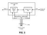
- FIG. 3is a block diagram of an embodiment of the power subsystem 211 of FIG. 2A or the power subsystem 231 of FIG. 2B .
- power subsystem 300is configured to route a power signal to and from a coil assembly coupled to the power subsystem 300 .
- the power subsystem 300is coupled to a first power bus PWR_IO and a second power bus PWR to transmit and receive power signals.
- Power subsystem 300is also coupled to a signal bus CTRL.
- the signal bus CTRLincludes signal lines CTR_IO, CTR_BRG, SENS_PWR_IO, and SENS_PWR.
- the power subsystem 300includes power input/output (I/O) circuitry 301 coupled to PWR_IO and a bridge circuit 302 coupled to PWR.
- the power I/O circuitry 301 and the bridge circuit 302are coupled together by another power bus.
- the power subsystem 300is fully bi-directional in that it may receive an input power signal via PWR_IO to generate an output power signal via PWR or alternatively, it may receive a power signal via PWR to generate an output power signal via PWR_IO.
- PWR_IOmay be coupled to other circuitry within an electronic device in which the power system 300 is implemented such as electronic device 205
- PWRmay be coupled to a coil assembly such as coil assembly 233
- CTRLmay be coupled to control circuitry such as control circuitry 232 .
- the power I/O circuitry 301includes switches, filters, and sense elements (not shown) to properly direct a power signal from PWR_IO to the bridge circuit 302 or vice-versa.
- the power I/O circuitry 301generates one or more sense signals SENS_PWR_IO which is transmitted via the signal bus CTRL.
- the sense signals SENS_PWR_IOcould be indicative of a voltage level within the power I/O circuit 301 , a current level of a power signal within the power I/O circuit 301 , or both.
- the power I/O circuitry 301receives one or more control signals CTRL_IO via the signal bus CTRL.
- the one or more control signalsoperate the switches within the power I/O circuitry 301 to properly direct power signals flowing through the power I/O circuitry 301 .
- the bridge circuit 302includes one or more electronically controlled switches (not shown) to perform signal processing functions on a power signal.
- the bridge circuit 302is configured to selectively perform AC to DC conversion or DC to AC conversion based on control signals CTRL_BRG received from via the signal bus CTRL.
- the control signals CTRL_BRGis indicative of a mode of operation of an inductive signal interface in which the power subsystem 300 is implemented (such as inductive signal interface 205 of FIG. 2B ).
- the bridge circuit 302generates sense signals SENS_PWR which is transmitted via the signal bus CTRL.
- the sense signals SENS_PWRcould be indicative of a voltage variation within the bridge circuit 302 , a current level of a power signal within the bridge circuit 302 , or both.
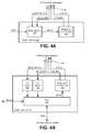
- FIG. 4Aillustrates control circuitry, according to an embodiment.
- Control circuitry 400may be an embodiment of the control circuitry 212 of FIG. 2A .
- the control circuitry 400is configured to receive sense signals from a bridge circuit and power I/O circuitry and in response thereto, the control circuitry 400 generates and transmits one or more control signals to the bridge circuit and the power I/O circuitry.
- Control circuitry 400has inputs to receive input control signal CTR_IN and sense signals SENS_PWR_IO and SENS_PWR, and has outputs to transmit signals control signals CTR_IO and CTR_BRG.
- Control circuitry 400includes a mode selector 401 and a bridge and I/O control circuit 402 . Referring back to FIG. 2A , signals SENS_PWR_IO, SENS_PWR, CTR_BRG, and CTR_IO are all transmitted or received via a signal bus CTRL to and from the power subsystem 211 .
- Mode selector 401receives the input control signal CTR_IN and the sense signals SENS_PWR_IO and SENS_PWR and generates signal MODE indicating a mode of operation of an inductive signal interface such as the inductive signal interface 230 of FIG. 2B .
- Signal MODEmay indicate a power transmit mode, a power receive mode, or an idle mode of the inductive signal interface.
- the input control signal CTR_INis a control signal generated by an electronic device such as electronic device 205 of FIG. 2B .
- the input control signal CTR_INmay indicate a command from the electronic device for the inductive signal interface to operate in a specific mode of operation.
- CTR_INmay indicate to the mode selector 401 to generate a signal indicating the mode of operation to be the power transmit mode.
- Sense signals SENS_PWR_IO and SENS_PWRare received from power I/O circuitry (such as power I/O circuitry 301 of FIG. 3 ) and a bridge circuit (such as bridge circuit 302 of FIG. 3 ), respectively. Each may indicate a current or voltage level within those circuit elements.
- Bridge and I/O control circuit 402receives the signal MODE and in accordance therewith generates control signals CTR_BRG and CTR_IO that control the operations of the bridge circuit and the power I/O circuitry, respectively.
- FIG. 4Billustrates another embodiment of control circuitry.
- Control circuitry 410may be an embodiment of the control circuitry 232 of FIG. 2B .
- the control circuitry 410is configured to receive sense signals from a bridge circuit and power I/O circuitry and in response thereto, the control circuitry 410 generates and transmits one or more control signals to the bridge circuit and the power I/O circuitry.
- the control circuitry 410is also configured to transmit and receive data signals via a communication subsystem.
- the control circuitry 410has inputs to receive sense signals SENS_PWR_IO and SENS_PWR, and has outputs to transmit signals control signals CTR_IO and CTR_BRG.
- Control circuitry 410also has bi-directional ports coupled to signal buses CPU_IO and DATA. Referring back to FIG. 2B , signals SENS_PWR_IO, SENS_PWR, CTR_BRG, and CTR_IO are transmitted or received via a signal bus CTRL to and from the power subsystem 231 , and signal bus DATA is coupled to the communications subsystem 234 .
- Control circuitry 410includes a CPU 411 , a DC sense 412 , an AC sense 413 , and bridge and I/O control circuit 414 .
- the CPU 411is coupled to signal buses CPU_IO and DATA.
- the signal bus CPU_IOmay be coupled to elements within an electronic device such as electronic device 205 of FIG. 2B to allow the CPU 411 to communicate with the electronic device.
- the signal bus DATAis coupled to a communication system such as the communication system 234 of FIG. 2B .
- the DC sense element 412is coupled between the input sense signal line SENS_PWR_IO and the CPU.
- the AC sense element 413is coupled between the input sense signal line SENS_PWR and the CPU 411 .
- the bridge and I/O control circuit 414is coupled between the CPU 411 and the output control signal lines CTR_BRG and CTR_IO.
- DC sense element 412 and AC sense element 413receive sense signals SENS_PWR_IO and SENS_PWR, respectively.
- Sense signal SENS_PWR_IOindicates a current flow or voltage level of on corresponding DC signal line while sense signal SENS_PWR indicates a current flow or voltage level on a corresponding AC signal line.
- the AC and DC signal linesare external to the control circuitry 410 .
- the DC sense element 412makes one or more determinations including a determination of whether a DC signal is detected on the corresponding DC signal line.
- the AC sense element 413makes one or more determinations include a determination of whether an AC signal is detect on the corresponding AC signal line.
- the DC sense element 412 and AC sense element 413transmit signals corresponding to those determinations to the CPU 411 .
- the CPU 411uses the determinations received from the AC and DC sense elements 413 and 412 to generate a MODE signal.
- the MODE signalcorresponds with information including a mode of operation of an inductive signal interface such as the inductive signal interface 230 of FIG. 2B .
- the MODE signalis received by the bridge and I/O control circuit 414 , and based on the MODE signal the bridge and I/O control circuit 414 generates control signals CTR_BRG and CTR_IO.
- the control signal CTR_BRGis outputted to a bridge circuit such as the bridge circuit 302 of FIG. 3 and controls the operation of the bridge circuit.
- the control signal CTR_IOis transmitted to power I/O circuitry such as the power I/O circuitry 301 of FIG. 3 and controls the operation of the control I/O circuitry.
- FIG. 5illustrates a bridge circuit, according to an embodiment.
- Bridge circuit 500may be an embodiment of the bridge circuit 302 of FIG. 3 , and as described with respect thereto, the bridge circuit 500 is configured to convert an AC power signal from a coil assembly to a DC power signal, or vice-versa.
- Bridge circuit 500as an I/O port coupled to a signal line IN_OUT to transmit or receive a power signal from the power I/O circuitry 301 of FIG. 3 .
- the bridge circuit 500is coupled to a coil assembly 510 through a signal bus PWR.
- Coil assembly 510is an embodiment of the coil assembly 213 of FIG. 2A or coil assembly 233 of FIG. 2B .
- the bridge circuit 500includes electrically controlled switches 501 , 502 , 503 , and 504 .
- Switch 501is coupled between IN_OUT and a node N 1
- switch 502is coupled between node N 1 and ground potential
- Switch 503is coupled between IN_OUT and a node N 2
- switch 504is coupled between node N 2 and ground potential.
- the signal bus PWRare coupled to nodes N 1 and N 2 and accordingly, the coil assembly 510 is coupled to the bridge circuit at node N 1 and at node N 2 .
- Sense signals SENS_PWR[ 1 ] and SENS_PWR[ 2 ]are also coupled to nodes N 1 and N 2 , respectively.
- SENS_PWR[ 1 ] and SENS_PWR[ 2 ]are transmitted via signal bus SENS_PWR to control circuitry 232 of FIG. 2B for example.
- SENS_PWR[ 1 ] and SENS_PWR[ 2 ]may be used to determine a voltage variation between nodes N 1 and N 2 .
- Each of the switches 501 - 504receives a respective control signal from the control signal bus CTR_BRG.
- switch 501receives signal CTR_BRG[ 1 ] and switch 503 receives signal CTR_BRG[ 3 ].
- Each of the control signalsindicate whether a corresponding switch should be open or closed. When a switch is closed, no current flows through the switch and when the switch is open, the switch is conductive, allowing a current to flow through the two nodes coupled to the switch.
- the control signals CTR_BRGare generated by control circuitry such as the control circuitry 232 of FIG. 2B .
- the control signals CTR_BRGoperate the switches 501 - 504 in manners that properly route a power signal from IN_OUT to the coil assembly and vice versa.
- the electrically controlled switches 501 , 502 , 503 , and 504are implemented using metal-oxide semiconductor field effect transistors (MOSFETs).
- MOSFETsmetal-oxide semiconductor field effect transistors
- each of the MOSFETsreceive a corresponding one of the control signals CTR_BRG[ 1 . . . 4 ] via a gate terminal.
- Power signal transmitted over the signal bus IN_OUTis a DC power signal while power signal transmitted to and from the coil assembly 510 is an AC power signal.
- the bridge circuit 500may operate in either in an H-bridge mode to perform DC to AC conversion or in a Sync-bridge mode to perform AC to DC conversion.
- the bridge circuit 500is operable in both the power receive and power transmit modes of an inductive signal interface, such as the inductive signal interface 230 of FIG. 2B . More specifically, the bridge circuit 500 operates in the H-bridge mode during the power transmit mode of the inductive signal interface and in the Sync-bridge mode during the power receive mode of the inductive signal interface.
- the control signals CTR_BRGselectively turn on one pair of switches within switches 501 - 504 while another pair of switches is turned off to perform AC to DC or DC to AC conversions.
- switches 501 and 504form a switch pair and switches 502 and 503 form another switch pair.
- switches 501 and 504are turned on, switches 502 and 504 are turned off and vice versa.
- the bridge circuit 500is capable of changing a current path of a power signal to perform AC to DC or DC to AC conversion. More specifically, in the H-bridge mode, the bridge circuit 500 receives a DC current via the signal bus IN_OUT and selectively operates the pairs of switches to alternate the direction of current flow to the coil assembly 510 over the PWR bus. For example, when switches 501 and 504 are on or closed, current flows from IN_OUT through switch 501 and node N 1 to reach the coil assembly 510 . On the other hand, when switches 503 and 502 are on or closed, current flows from IN_OUT through 503 and node N 2 to reach the coil assembly 510 .
- the bridge circuit 500By alternating the direction of current flow to the coil assembly 510 , the bridge circuit 500 performs DC to AC conversion and transmits an AC power signal to the coil assembly 510 . Similarly, in the Sync-bridge mode, the bridge circuit 500 selectively operates the switches 501 - 504 to perform AC to DC conversion. In some embodiments, IN_OUT is coupled to a low pass filter as part of the AC to DC conversion process.
- Voltage variation between nodes N 1 and N 2may be used to determine how to operate the switches 501 - 504 .
- switches 501 and 504may be turned on to ensure correct direction of current flow to IN_OUT.
- Voltage variation between N 1 and N 2may also indicate that the coil assembly 510 is being inductively or resonantly coupled to a coil on another device. Accordingly, this voltage variation may be used by control circuitry (such as control circuitry 232 of FIG.
- the switch pairsmay be periodically turned on and off based on a frequency of the AC signal transmitted over the signal bus PWR.
- the bridge circuit 500can also enter an off mode which may correspond with the aforementioned idle or communication-only modes of the inductive signal interface. During the off mode, all switches 501 , 502 , 503 , and 504 receive a control voltage corresponding to an off state for the switches. According some embodiments, before entering the off mode, the bridge circuit 500 is configured to turn off the switches 501 - 504 individually to prevent back current from the coil assembly.
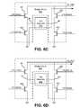
- FIG. 6Aillustrates a current path through the bridge circuit 500 and coil assembly 510 of FIG. 5 while the bridge circuit is operating in the H-bridge mode.
- a DC power signalis received via signal line IN_OUT.
- Switches 502 and 503are on while switches 501 and 504 are off.
- the power signalflows through switch 503 and node N 2 to the coil assembly 510 .
- FIG. 6Billustrates another current path through the bridge circuit 500 and coil assembly 510 of FIG. 5 while the bridge circuit is operating in the H-bridge mode.
- a DC power signalis received via signal line IN_OUT.
- Switches 501 and 504are on while switches 502 and 503 are off.
- the power signalflows through switch 501 and node N 1 to the coil assembly 510 .
- FIG. 6Cillustrates a current path through the bridge circuit 500 and coil assembly 510 of FIG. 5 while the bridge circuit is operating in the Sync-bridge mode.
- An AC power signalis received from coil assembly 510 .
- the depicted current pathis active when the AC power signal received from coil assembly 510 has a higher voltage at node N 2 than at node N 1 .
- Switches 502 and 503are on while switches 501 and 504 are off. Current flows from ground potential through switch 502 and node N 1 to the coil assembly 510 . Current exits coil assembly 510 at node N 2 and flows through switch 503 to reach signal bus IN_OUT.
- FIG. 6Dillustrates another current path through the bridge circuit 500 and coil assembly 510 of FIG. 5 while the bridge circuit is operating in the Sync-bridge mode.
- An AC power signalis received from coil assembly 510 .
- the depicted current pathis active when the AC power signal received from coil assembly 510 has a higher voltage at node N 1 than at node N 2 .
- Switches 501 and 504are on while switches 502 and 503 are off. Current flows from ground potential through switch 504 and node N 2 to the coil assembly 510 . Current exits coil assembly 510 at node N 1 and flows through switch 501 to reach signal bus IN_OUT.
- FIG. 7is a block diagram of power I/O circuitry, according to an embodiment.
- Power I/O circuitry 700may be an embodiment of the power I/O circuitry 301 of FIG. 3 . As described with respect to FIG. 3 , the power I/O circuitry 700 is configured to direct a power signal from a power signal line to a bridge circuit or vice-versa.
- the power I/O circuitry 700has inputs coupled to a signal bus CTR_IO, outputs to transmit signals LOGIC_PWR and a signal bus SENS_PWR_IO, and an I/O port coupled to a power signal line PWR.
- the power I/O circuitry 700also has an input to receive an input power signal PWR_IN and an output to transmit output power signals PWR_OUT and PWR_BATT.
- the power I/O circuitry 700includes a low pass filter 701 , a current sense element 702 , switching converters 704 and 705 , a diode 706 , a voltage regulator 707 , and a over-voltage-protection (OVP) switch 708 .
- the low pass filter 701is coupled between the signal line PWR and the OVP switch 708 .
- the current sense element 702is coupled to the OVP switch and also has an input coupled to the switching converter 704 and an output coupled to the switching converter 705 .
- the current sense element 702also has an output coupled to signal line I_SENS which a signal line within the signal bus SENS_PWR_IO.
- the switching converter 704is coupled between the current sense element 702 and the input power signal line PWR_IN.
- the switching converter 705is coupled between the current sense element 702 and the output power signal line PWR_OUT.
- the diode 706is coupled between the input power signal line PWR_IN and the voltage regulator 707 which has an output to generate the output signal LOGIC_PWR.
- Output power signal line PWR_OUTis coupled to an output signal line OUTPUT_SENS which a signal line within signal bus SENS_PWR_IO.
- Switching converters 704 and 705receive and are controlled by controls signals IN_EN and OUT_EN which are signals which are signals within the signal bus CTR_IO. According to one embodiment, the switching converters 704 and 705 each receives an input signal and operates to transmit an output signal which is at a different voltage level than the input signal.
- the switching converter 704is coupled to receive an input power signal through power signal line PWR_IN and transmits an output power signal to the current sense element 702 .
- the switching converter 705receives an input signal from the current sense element 702 and transmits an output power signal via the power signal line PWR_OUT.
- the switching converters 704 and 705can each operate in an off position to act as a shunt, allowing no signals to pass through.
- the switching converters 704 and 705each includes one or more FETs.
- the OVP switch 708is configured to enter an off (i.e. non-conductive) state when it is detected that a voltage exceeds a predetermined threshold, in order to protect elements of the power subsystem 700 from damage from high voltages. Otherwise, the OVP switch 708 operates in an on (i.e. conductive) state. For one embodiment, the OVP switch 708 is configured to enter the off state when the voltage on the power signal line PWR exceeds the predetermined threshold.
- the power subsystem 700is configured to direct received power signals to desired outputs and to output sense signals that indicate a current flow (or voltage) of the received power signals and output power signals. Referring back to FIGS. 2A and 2B , the power subsystem 700 can be coupled to control circuitry such as the control circuitry 232 of FIG. 2B and to a coil assembly such as the coil assembly 233 of FIG. 2B .
- an input power signalis received via the input power signal line PWR_IN.
- the switch 704is configured to enter or remain in the closed state by the control signal 704 .
- the input power signalpropagates through the switch 704 to the current sense element 702 .
- the current sense element 702outputs power signals to the low pass filter and the switch 705 .
- the switch 705is configured to enter or remain in the open state by the control signal OUT_EN and thus does not conduct any current.
- the low pass filter 701receives power signals transmitted by the current sense element 702 and operates to eliminate frequency components above a certain threshold to output an output power signal to the power signal line PWR.
- Current sense element 702also transmits a power signal to the output power signal line PWR_BATT which, according to some embodiments, is coupled to a battery or to battery charging circuitry.
- the diode 706also receives input power signal via the input power signal line PWR_IN.
- the diode 706allows current to propagate to the voltage regulator 707 which operates to maintain a constant voltage level at its output LOGIC_PWR.
- Signal line LOGIC_PWRcan be coupled to transmit a power signal to circuit components to provide those components with a source of power.
- an input power signalis received via the power signal line PWR.
- the low pass filter 701receives the input power signal and operates to eliminate frequency components above a certain threshold to transmit a filtered power signal to the current sense element 702 .
- the current sense element 702transmits a first output power signal via the output power signal line PWR_BATT and a second output power signal to the switch 705 .
- the switch 705is configured to enter or remain in the closed state by the control signal OUT_EN and the second output power signal is propagated to the output power signal line PWR_OUT.
- the switch 704is configured to enter or remain in the open state and does not conduct any current.
- the current sense element 702In each of the aforementioned modes of operation of the power subsystem 700 , the current sense element 702 generates the output sense signal I_SENS which indicates a current level of the signals received or transmitted by the current sense element 702 .
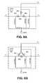
- FIG. 8Ais a circuit diagram illustrating a current sense element, according to an embodiment.
- a current sense elementmaybe used to determine one or more current flows such as described with an embodiment of FIG. 7 and may be an embodiment of the current sense element 702 of FIG. 7 .
- Current sense element 800has three terminals T 1 , T 2 , and T 3 and includes three resistors 801 , 802 , and 803 each having a pre-determined resistance value R.
- the resistors 801 , 802 , and 803are coupled between a common node 804 and a respective one of the terminals T 1 , T 2 , and T 3 .
- Resistor 801is coupled between node 804 and terminal T 1 .
- Resistor 802is coupled between node 804 and terminal T 2 .
- Resistor 803is coupled between node 804 and terminal T 3 .
- the current sense element 800also has an output coupled to a signal bus I_SENS.
- Signal bus I_SENSincludes three signals lines I_SENS[ 1 . . . 3 ], each being coupled to one of the terminals T 1 , T 2 , and T 3 .
- I_SENS[ 1 ]is coupled to terminal T 1 .
- I_SENS[ 2 ]is coupled to terminal T 2 .
- I_SENS[ 3 ]is coupled to terminal T 3 .
- the current sense element 800is configured to direct current from any of the terminals T 1 , T 2 , or T 3 to any other terminal. It also provides current flow information through the signals I_SENS[ 1 . . . 3 ]. More specifically, the current sense element 800 is able to detect current flow from between each of the three pairs of terminals (i.e. between T 1 and T 2 , between T 2 and T 3 , and between T 1 and T 3 ) by measuring the voltage at the terminals T 1 , T 2 , and T 3 .
- FIG. 8Bis a circuit diagram illustrating another embodiment of a current sense element.
- Current sense element 850may be an embodiment of the current sense element 702 of FIG. 7 .
- Current sense element 850has three terminals T 1 , T 2 , and T 3 and includes three resistors 851 , 852 , and 853 each having a pre-determined resistance value R.
- the resistor 851is coupled between terminals T 1 and T 2
- the resistor 852is coupled between terminals T 1 and T 3
- resistor 853is coupled between terminals T 2 and T 3 .
- the current sense element 850also has an output coupled to a signal bus I_SENS.
- Signal bus I_SENSincludes three signals lines I_SENS[ 1 . . .
- I_SENS[ 1 ]is coupled to terminal T 1 .
- I_SENS[ 2 ]is coupled to terminal T 2 .
- I_SENS[ 3 ]is coupled to terminal T 3 .
- the current sense element 850is configured to direct current from any of the terminals T 1 , T 2 , or T 3 to any other terminal. It also provides current flow information through the signals I_SENS[ 1 . . . 3 ]. More specifically, the current sense element 850 is able to detect current flow from between each of the three pairs of terminals (i.e. between T 1 and T 2 , between T 2 and T 3 , and between T 1 and T 3 ) by measuring the voltage at the terminals T 1 , T 2 , and T 3 .
- FIG. 9illustrates an embodiment of a coil assembly that can be configured to form an inductive link in the manner described throughout this application.
- Coil assembly 900may be an embodiment of the coil assembly 233 of FIG. 2B .
- the coil assembly 900includes a power coil 901 , and a communications coil 902 .
- the power coil 901 and the communication coil 902are separated by an air gap 903 .
- the power coilhas a terminal T_PWR.
- the communications coilhas a terminal T_COMM.
- the coil assembly 900may be coupled to a power subsystem such as the power subsystem 231 of FIG. 2B and to a communications subsystem such as the communications subsystem 234 of FIG. 2B .
- terminal T_PWRis coupled to the power subsystem
- terminal T_COMMis coupled to the communications subsystem.
- FIG. 10illustrates an embodiment of a communication subsystem which may be an embodiment of the communication subsystem 234 of FIG. 2B .
- communication subsystem 1000is configured to perform signal processing functions on data signals.
- the signal processing functionsmay include modulating a carrier frequency with the data signal, and de-modulating the data signals.
- the communication subsystem 1000has inputs to receive input data TX, a carrier signal CARRIER, an output to transmit output data RX, and a port coupled to bi-directional signal line COMM.
- the communication subsystem 1000includes a high-pass filter 1001 , a rectifier 1002 , a low pass filter 1003 , a threshold detector 1004 and a modulator 1005 .
- the high pass filter 1001has an input coupled to the bi-directional signal line COMM and an output coupled to an input of the rectifier 1002 .
- the rectifier 1002has an output coupled to an input of the low-pass filter 1003 which also has an output coupled to the input of the threshold detector 1004 .
- the threshold detector 1004has an output to transmit the output data signal RX.
- the modulator 1005has two inputs to receive the input data TX, and the carrier signal CARRIER. An output of the modulator 1005 is coupled to the bi-directional signal line COMM.
- the high pass filter 1001is coupled to the bi-directional signal line COMM to receive a communication signal and operates to eliminate low frequency components of the communication signal to generate a filtered communication signal.
- the rectifier 1002receives the filtered communication signal from the high pass filter 1001 , and performs AC to DC conversion on the filtered communication signal to generate a DC signal as an output.
- the rectifier 1002outputs the DC signal to the low pass filter 1003 .
- the low pass filter 1003operates to eliminate frequency components higher than a certain frequency threshold from the DC signal to generate an analog signal that is transmitted to the threshold detector 1004 .
- the threshold detector 1004digitizes the analog signal to generate the output data signal RX. According to some embodiments, the threshold detector 1004 digitizes the analog signal by detecting instances when the analog signal crosses a voltage threshold to generate a digital value of 1 for those instances and a digital value of 0 for time when the analog signal does not cross the voltage threshold.
- FIG. 11is a representative diagram illustrating two computing devices that can be brought into proximity for purpose of enabling one device to provide a power and/or data signal to the other device, according to an embodiment.
- Numerous embodiments described hereinmay be implemented using a mobile computing device and dock as two devices that are brought into proximity with one another for purpose of power/data transfer without use of traditional insertive or mechanically coupled connectors.
- different kinds of devicese.g. portable devices and accessory devices
- two devices that are inductively coupledcorrespond to a mobile computing device (also referred to as an “MCD”) and a dock or docking station.
- MCDmobile computing device
- dock or docking stationa dock or docking station.
- the MCDis a mufti-purpose device having cellular data and telephonic capabilities
- the accessory devicecorresponds to, for example, a docking station (for communications and power supply), sticky (or piggy)-back accessory, a light projector, a speaker set, or headset station.
- the MCDmay include, for example, functionality for use as a media player, a camera or video recorder, a global positioning unit, an ultra-mobile personal computer, a laptop computer, or a multi-purpose computing device. Numerous other examples and implementations are described herein, including embodiments in which three or more devices are interconnected through one or more connector-less connections.
- the dock 1120can be provided as an inductive landing pad or station of another device.
- the dock 1120may be provided as an integrated component of a printer, personal computer, portable computer (e.g. laptop), computer accessory, or vehicle dashboard.
- a system 1100includes a MCD 1110 that is supported or otherwise retained by a dock 1120 .
- the manner in which the MCD 1110 is supportedmay vary.
- the orientation of the MCD on the dockmay be changed by the user for purpose of configuring operations or behavior of one or both devices.
- the MCD 1110is supported on the dock 1120 in a partially upright position along its length axis (L).
- Such an orientationmay correspond to a ‘portrait’ position.
- one or more ‘landscape’ positions, or positions in between the portrait and landscape positionsmay be possible.
- the dock 1120utilizes physical support structures (not shown), such as shelves, platforms, hooks or mechanical retention features, to retain the MCD 1110 in a docked or mated position.
- physical support structuressuch as shelves, platforms, hooks or mechanical retention features
- magnetic claspsmay be included or provided the dock 1120 and/or the MCD 1110 to secure retention of the MCD against the dock.
- the dock 1120may include resources 1121 for generating or extending power and/or data signals to the MCD 1110 .
- the dock 1120may be mated with a power outlet 1124 or another computer 1126 (e.g. desktop computer) to extend power and/or data signals.
- the resources 1121may include circuitry or hardware, such as AC/DC converters and regulators.
- the dock 1120may include a physical connector port, such as provided by a Universal Serial Bus (USB) connector.
- USBUniversal Serial Bus
- the dock 1120may include data acquisition capabilities, provided through connector ports with the computer 1126 , wireless ports (e.g. cellular, WiMax connection, Bluetooth), Internet ports, and media feeds (e.g. provided through television tuner and cable).
- the MCD 1110has a housing shell 1112 having a thickness (t).
- the housing shell 1112may be used to retain internal components of the MCD 1110 , such as a circuit board, processor, memory, or components of a display assembly.
- the MCD 1110may be structured so that a primary facade 1115 (e.g. the back panel) of the housing shell 1112 rests on a receiving surface 1125 of the dock 1120 .
- the two computing devicesare each provided an inductive signal interface 1119 , 1129 for enabling one device to inductively transmit power to the other device.
- the inductive signal interface 1119 , 1129 of each devicemay be implemented using a bridge circuit such as described with FIGS. 6A to 6D and elsewhere in this application. In this manner, embodiments described herein provide a system and technique for delivering electrical power from over short distances without the use of electrical conductors
- FIG. 11depicts two computing devices that use the inductive signal interface to inductively couple and signal power
- other embodimentsprovide for use of other computing devices and device pairings.
- the two inductively paired devicesmay correspond to a mobile computing device and headset, two mobile computing devices, or mobile computing device and power-resourced holster.
- Embodiments described hereininclude individual elements and concepts described herein, independently of other concepts, ideas or systems, as well as combinations of elements recited anywhere in this application. Although illustrative embodiments of the invention have been described in detail with reference to the accompanying drawings, it is to be understood that the described embodiments are not limited to those precise embodiments, but rather include modifications and variations as provided. Furthermore, a particular feature described either individually or as part of an embodiment can be combined with other individually described features, or parts of other embodiments, even if the other features and embodiments make no mention of the particular feature.
Landscapes
- Engineering & Computer Science (AREA)
- Power Engineering (AREA)
- Computer Networks & Wireless Communication (AREA)
- Signal Processing (AREA)
- Charge And Discharge Circuits For Batteries Or The Like (AREA)
Abstract
Description
Claims (19)
Priority Applications (1)
| Application Number | Priority Date | Filing Date | Title |
|---|---|---|---|
| US12/841,001US8437695B2 (en) | 2009-07-21 | 2010-07-21 | Power bridge circuit for bi-directional inductive signaling |
Applications Claiming Priority (4)
| Application Number | Priority Date | Filing Date | Title |
|---|---|---|---|
| US22741309P | 2009-07-21 | 2009-07-21 | |
| US22742309P | 2009-07-21 | 2009-07-21 | |
| US12/628,401US8954001B2 (en) | 2009-07-21 | 2009-12-01 | Power bridge circuit for bi-directional wireless power transmission |
| US12/841,001US8437695B2 (en) | 2009-07-21 | 2010-07-21 | Power bridge circuit for bi-directional inductive signaling |
Related Parent Applications (1)
| Application Number | Title | Priority Date | Filing Date |
|---|---|---|---|
| US12/628,401Continuation-In-PartUS8954001B2 (en) | 2009-07-21 | 2009-12-01 | Power bridge circuit for bi-directional wireless power transmission |
Publications (2)
| Publication Number | Publication Date |
|---|---|
| US20110037321A1 US20110037321A1 (en) | 2011-02-17 |
| US8437695B2true US8437695B2 (en) | 2013-05-07 |
Family
ID=43588163
Family Applications (1)
| Application Number | Title | Priority Date | Filing Date |
|---|---|---|---|
| US12/841,001Active2030-07-14US8437695B2 (en) | 2009-07-21 | 2010-07-21 | Power bridge circuit for bi-directional inductive signaling |
Country Status (1)
| Country | Link |
|---|---|
| US (1) | US8437695B2 (en) |
Cited By (8)
| Publication number | Priority date | Publication date | Assignee | Title |
|---|---|---|---|---|
| US20120276963A1 (en)* | 2011-04-29 | 2012-11-01 | Tyfone, Inc. | Coupling area enhancement apparatus, system, and method |
| US20130308256A1 (en)* | 2011-03-09 | 2013-11-21 | Hewlett-Packard Development Company, L.P. | Flat power coil for wireless charging applications |
| US8850045B2 (en) | 2008-09-26 | 2014-09-30 | Qualcomm Incorporated | System and method for linking and sharing resources amongst devices |
| US10439449B2 (en) | 2016-08-10 | 2019-10-08 | Microsoft Technology Licensing, Llc | Coupling device modules for inductive data transmission |
| TWI739683B (en)* | 2020-12-01 | 2021-09-11 | 瑞昱半導體股份有限公司 | Electronic device system and power delivery method |
| US11757490B2 (en) | 2018-08-02 | 2023-09-12 | Fraunhofer-Gesellschaft zur Förderung der angewandten Forschung e.V | Data transmission from a user terminal to another apparatus |
| US12096167B2 (en) | 2019-01-30 | 2024-09-17 | Fraunhofer-Gesellschaft Zur Foerderung Der Angewandten Forschung E.V. | Bidirectional configuration of sensor nodes with mobile phone with no extension |
| US12294422B2 (en) | 2019-05-10 | 2025-05-06 | Fraunhofer-Gesellschaft zur Förderung der angewandten Forschung e.V. | Efficient communication to configure sensor nodes |
Families Citing this family (11)
| Publication number | Priority date | Publication date | Assignee | Title |
|---|---|---|---|---|
| US8395547B2 (en) | 2009-08-27 | 2013-03-12 | Hewlett-Packard Development Company, L.P. | Location tracking for mobile computing device |
| US8755815B2 (en) | 2010-08-31 | 2014-06-17 | Qualcomm Incorporated | Use of wireless access point ID for position determination |
| CN103222319B (en) | 2010-09-29 | 2016-08-10 | 高通股份有限公司 | A kind of method for mobile computing device and mobile computing device |
| FR2980055B1 (en)* | 2011-09-12 | 2013-12-27 | Valeo Systemes Thermiques | INDUCTIVE POWER TRANSMISSION DEVICE |
| KR20130134759A (en)* | 2012-05-31 | 2013-12-10 | 엘에스전선 주식회사 | Flexible circuit board for dual-mode antenna, dual-mode antenna and user device |
| US9248751B2 (en)* | 2013-03-15 | 2016-02-02 | Qualcomm Incorporated | Mixed semiconductor H-bridge power converters and methods related thereto |
| US20150130290A1 (en)* | 2013-11-11 | 2015-05-14 | Samsung Electro-Mechanics Co., Ltd. | Wireless power transmitting apparatus and wireless power transmitting-receiving apparatus |
| US20180062417A1 (en)* | 2015-03-03 | 2018-03-01 | Amogreentech Co., Ltd. | Case for portable terminal having built-in battery |
| JP2018507678A (en)* | 2015-03-06 | 2018-03-15 | パワーバイプロキシ リミテッド | Wireless power transfer adapter |
| JP6696221B2 (en)* | 2016-02-26 | 2020-05-20 | セイコーエプソン株式会社 | Control device, power receiving device, electronic device, and power transmission system |
| US10439439B2 (en)* | 2017-02-13 | 2019-10-08 | STMicroelectronics (Grand Ouest) SAS | Method and device for the contactless energy transfer to an apparatus equipped with a loudspeaker |
Citations (122)
| Publication number | Priority date | Publication date | Assignee | Title |
|---|---|---|---|---|
| FR2601161A1 (en) | 1986-07-02 | 1988-01-08 | Crouzet Sa | Information processing device |
| US5375226A (en) | 1988-12-29 | 1994-12-20 | Toppan Moore Company, Ltd. | Portable type data entry terminal having a keyboard input device and a graphic input device |
| WO1995003686A1 (en) | 1993-07-23 | 1995-02-02 | Steven James Shattil | Active electromagnetic shielding |
| US5455466A (en) | 1993-07-29 | 1995-10-03 | Dell Usa, L.P. | Inductive coupling system for power and data transfer |
| US5596567A (en) | 1995-03-31 | 1997-01-21 | Motorola, Inc. | Wireless battery charging system |
| US5600225A (en) | 1994-06-30 | 1997-02-04 | Nippon Electric Co | Noncontacting charging device |
| US5666530A (en) | 1992-12-02 | 1997-09-09 | Compaq Computer Corporation | System for automatic synchronization of common file between portable computer and host computer via communication channel selected from a plurality of usable channels there between |
| US5733313A (en) | 1996-08-01 | 1998-03-31 | Exonix Corporation | RF coupled, implantable medical device with rechargeable back-up power source |
| US5760580A (en) | 1994-04-26 | 1998-06-02 | Rso Corporation N.V. | Method for excitation and detection of magnetic elements by a mechanical resonance |
| US5831348A (en) | 1996-06-03 | 1998-11-03 | Mitsubishi Denki Kabushiki Kaisha | Secondary circuit device for wireless transmit-receive system and induction coil for wireless transmit-receive system |
| US5958051A (en) | 1996-11-27 | 1999-09-28 | Sun Microsystems, Inc. | Implementing digital signatures for data streams and data archives |
| US6006274A (en) | 1997-01-30 | 1999-12-21 | 3Com Corporation | Method and apparatus using a pass through personal computer connected to both a local communication link and a computer network for indentifying and synchronizing a preferred computer with a portable computer |
| US6138245A (en) | 1999-02-05 | 2000-10-24 | Neopoint, Inc. | System and method for automatic device synchronization |
| US6184651B1 (en) | 2000-03-20 | 2001-02-06 | Motorola, Inc. | Contactless battery charger with wireless control link |
| JP3161388B2 (en) | 1997-11-05 | 2001-04-25 | 日本電気株式会社 | Docking bay system |
| US6266539B1 (en) | 1998-06-12 | 2001-07-24 | Cisco Technology, Inc. | Telephone docking station for personal digital assistant |
| US6330436B1 (en) | 1999-04-30 | 2001-12-11 | Lucent Technologies, Inc. | Enhanced wireless messaging notification system |
| US6389423B1 (en) | 1999-04-13 | 2002-05-14 | Mitsubishi Denki Kabushiki Kaisha | Data synchronization method for maintaining and controlling a replicated data |
| US6400274B1 (en) | 1995-08-31 | 2002-06-04 | Intermec Ip Corp. | High-performance mobile power antennas |
| US6405049B2 (en) | 1997-08-05 | 2002-06-11 | Symbol Technologies, Inc. | Portable data terminal and cradle |
| US20020084698A1 (en) | 2000-11-20 | 2002-07-04 | Kelly Clifford Mark | Electrically isolated power and signal coupler system for a patient connected device |
| US20020103008A1 (en) | 2001-01-29 | 2002-08-01 | Rahn Michael D. | Cordless communication between PDA and host computer using cradle |
| US6436299B1 (en) | 1999-06-21 | 2002-08-20 | Amway Corporation | Water treatment system with an inductively coupled ballast |
| US6445936B1 (en) | 1999-11-16 | 2002-09-03 | Agere Systems Guardian Corp. | Low power consumption quick charge for wireless device |
| US6501364B1 (en) | 2001-06-15 | 2002-12-31 | City University Of Hong Kong | Planar printed-circuit-board transformers with effective electromagnetic interference (EMI) shielding |
| US6510424B1 (en) | 1999-10-22 | 2003-01-21 | International Business Machines Corporation | Electronic notification agent |
| US6532152B1 (en) | 1998-11-16 | 2003-03-11 | Intermec Ip Corp. | Ruggedized hand held computer |
| US20030214255A1 (en) | 1999-06-21 | 2003-11-20 | Baarman David W. | Inductively powered apparatus |
| US20030233455A1 (en) | 2002-06-14 | 2003-12-18 | Mike Leber | Distributed file sharing system |
| US6673250B2 (en) | 1999-06-21 | 2004-01-06 | Access Business Group International Llc | Radio frequency identification system for a fluid treatment system |
| US6731071B2 (en) | 1999-06-21 | 2004-05-04 | Access Business Group International Llc | Inductively powered lamp assembly |
| US20040088012A1 (en) | 2002-10-30 | 2004-05-06 | Kroll Mark W. | Implantable stimulation device with isolating system for minimizing magnetic induction |
| US20040130915A1 (en) | 1999-06-21 | 2004-07-08 | Baarman David W. | Adaptive inductive power supply with communication |
| US20040130916A1 (en) | 1999-06-21 | 2004-07-08 | Baarman David W. | Adaptive inductive power supply |
| US20040150934A1 (en) | 2003-02-04 | 2004-08-05 | Baarman David W. | Adapter |
| US6795110B1 (en) | 1999-06-15 | 2004-09-21 | Philip Kossin | Weatherproof and watertight digital electronic camera, including a solid or fluid-filled digital camera operating at great depths |
| US6803744B1 (en) | 1999-11-01 | 2004-10-12 | Anthony Sabo | Alignment independent and self aligning inductive power transfer system |
| US6806649B2 (en) | 2002-02-19 | 2004-10-19 | Access Business Group International Llc | Starter assembly for a gas discharge lamp |
| US6810405B1 (en) | 1998-08-18 | 2004-10-26 | Starfish Software, Inc. | System and methods for synchronizing data between multiple datasets |
| WO2004098079A1 (en) | 2003-04-25 | 2004-11-11 | Apple Computer Inc. | Media player system |
| US6825620B2 (en) | 1999-06-21 | 2004-11-30 | Access Business Group International Llc | Inductively coupled ballast circuit |
| US20040259499A1 (en) | 2001-07-18 | 2004-12-23 | Haruo Oba | Communication system and method |
| US20040266362A1 (en) | 2003-06-27 | 2004-12-30 | Watkins Ronald Dean | Transmit/receive switch |
| US20050007067A1 (en) | 1999-06-21 | 2005-01-13 | Baarman David W. | Vehicle interface |
| CN1592197A (en) | 2003-09-01 | 2005-03-09 | 台均实业有限公司 | Method for authentication between client device and local client application or remote network service |
| US6888438B2 (en) | 2001-06-15 | 2005-05-03 | City University Of Hong Kong | Planar printed circuit-board transformers with effective electromagnetic interference (EMI) shielding |
| GB2389720B (en) | 2002-06-10 | 2005-09-07 | Univ City Hong Kong | Planar inductive battery charger |
| GB2399466B (en) | 2003-03-10 | 2005-11-16 | Univ City Hong Kong | Battery charging system |
| US6975198B2 (en) | 2003-02-04 | 2005-12-13 | Access Business Group International Llc | Inductive coil assembly |
| US6986051B2 (en) | 2000-04-13 | 2006-01-10 | International Business Machines Corporation | Method and system for controlling and filtering files using a virus-free certificate |
| US20060041420A1 (en) | 2004-06-30 | 2006-02-23 | Threshold Corporation | Method and apparatus for configuring a network appliance |
| US20060061958A1 (en) | 2004-09-17 | 2006-03-23 | Mark Solomon | Portable computer docking station |
| GB2389767B (en) | 2002-06-10 | 2006-04-19 | Univ City Hong Kong | Apparatus for energy transfer by induction |
| US20060123055A1 (en) | 2004-12-07 | 2006-06-08 | Paul Atkinson | Device and method for selectively controlling the utility of a target |
| US7065658B1 (en) | 2001-05-18 | 2006-06-20 | Palm, Incorporated | Method and apparatus for synchronizing and recharging a connector-less portable computer system |
| US20060132045A1 (en) | 2004-12-17 | 2006-06-22 | Baarman David W | Heating system and heater |
| US20060187049A1 (en) | 2005-02-09 | 2006-08-24 | Atmel Germany Gmbh | Circuit arrangement and method for supplying power to a transponder |
| US7149473B1 (en) | 1999-01-15 | 2006-12-12 | Nokia Corporation | Interface |
| US7164255B2 (en) | 2002-06-10 | 2007-01-16 | City University Of Hong Kong | Inductive battery charger system with primary transformer windings formed in a multi-layer structure |
| US20070035917A1 (en) | 2005-08-09 | 2007-02-15 | Apple Computer, Inc. | Methods and apparatuses for docking a portable electronic device that has a planar like configuration and that operates in multiple orientations |
| US20070064406A1 (en) | 2003-09-08 | 2007-03-22 | Beart Pilgrim G W | Inductive power transfer units having flux shields |
| WO2007034421A2 (en) | 2005-09-23 | 2007-03-29 | Ipico Innovation Inc. | Radio frequency identification device systems |
| US20070120752A1 (en) | 2005-11-30 | 2007-05-31 | Nobuaki Takasu | Information processing apparatus, information processing system and radio communication control method |
| US7248017B2 (en) | 2002-05-13 | 2007-07-24 | Spashpower Limited | Portable contact-less power transfer devices and rechargeable batteries |
| US20070182367A1 (en) | 2006-01-31 | 2007-08-09 | Afshin Partovi | Inductive power source and charging system |
| US20070188284A1 (en) | 2003-02-26 | 2007-08-16 | Dobbs John M | Shielded power coupling device |
| US7262700B2 (en) | 2005-03-10 | 2007-08-28 | Microsoft Corporation | Inductive powering surface for powering portable devices |
| US7271569B2 (en) | 2004-09-21 | 2007-09-18 | Motorola Inc. | Contact less charger with alignment indicator |
| US7286880B2 (en) | 2003-10-02 | 2007-10-23 | Medtronic, Inc. | System and method for transcutaneous energy transfer achieving high efficiency |
| US20070246546A1 (en) | 2006-04-20 | 2007-10-25 | Yuko Yoshida | Information Processing Terminal, IC Card, Portable Communication Device, Wireless Communication Method, and Program |
| US20070290654A1 (en) | 2006-06-14 | 2007-12-20 | Assaf Govari | Inductive charging of tools on surgical tray |
| US7323964B1 (en)* | 2006-11-23 | 2008-01-29 | National Central University | Non-contact power system with load and gap detection |
| US7331793B2 (en) | 2005-12-16 | 2008-02-19 | Motorola, Inc. | Magnetic connector |
| WO2008033670A2 (en) | 2006-09-11 | 2008-03-20 | Apple Inc. | Highly portable media devices |
| WO2008044875A1 (en) | 2006-10-10 | 2008-04-17 | Ls Cable, Ltd. | Rechargeable power supply, battery device, contact-less charger systems and method for charging rechargeable battery cell |
| US7375492B2 (en) | 2003-12-12 | 2008-05-20 | Microsoft Corporation | Inductively charged battery pack |
| US7382636B2 (en) | 2005-10-14 | 2008-06-03 | Access Business Group International Llc | System and method for powering a load |
| US20080133918A1 (en) | 2006-12-04 | 2008-06-05 | Samsung Electronics Co., Ltd. | Method and apparatus for transmitting data using authentication |
| KR100836634B1 (en) | 2006-10-24 | 2008-06-10 | 주식회사 한림포스텍 | Portable terminal using a contactless charger, a battery pack for charging and a contactless charger for wireless data communication and power transmission |
| US7385357B2 (en) | 1999-06-21 | 2008-06-10 | Access Business Group International Llc | Inductively coupled ballast circuit |
| US7392059B2 (en) | 2001-05-14 | 2008-06-24 | Innovision Research & Technology Plc | Electrical devices |
| US20080196086A1 (en) | 2007-02-09 | 2008-08-14 | Sony Corporation, A Japanese Corporation | Method and apparatus for authorizing a communication interface |
| US7414380B2 (en) | 2004-09-21 | 2008-08-19 | Lear Corporation | Apparatus for inductively recharging batteries of a portable convenience device |
| US20080231537A1 (en) | 2007-03-19 | 2008-09-25 | Ahmadreza Rofougaran | Method and system for fm transmit and fm receive using a transformer as a duplexer |
| US7446672B2 (en) | 2005-03-24 | 2008-11-04 | M&Fc Holding, Llc | Method and apparatus for coupling a meter register to an automatic meter reading communication device |
| WO2008133806A1 (en) | 2007-04-23 | 2008-11-06 | Eastman Kodak Company | Charging display system |
| US20080278894A1 (en) | 2007-05-11 | 2008-11-13 | Miradia Inc. | Docking station for projection display applications |
| US7454170B2 (en) | 2003-08-08 | 2008-11-18 | Koninklijke Philips Electronics N.V. | Unidirectional power and bi-directional data transfer over a single inductive coupling |
| US7462951B1 (en) | 2004-08-11 | 2008-12-09 | Access Business Group International Llc | Portable inductive power station |
| US7471986B2 (en) | 2004-02-20 | 2008-12-30 | Cardiac Pacemakers, Inc. | System and method for transmitting energy to and establishing a communications network with one or more implanted devices |
| US20090001932A1 (en) | 2007-06-29 | 2009-01-01 | Seiko Epson Corporation | Power transmission control device, power transmission device, non-contact power transmission system, and electronic instrument |
| US20090001941A1 (en) | 2007-06-29 | 2009-01-01 | Microsoft Corporation | Inductive Powering Surface for Powering Portable Devices |
| US20090008148A1 (en) | 2007-07-03 | 2009-01-08 | Shinko Electric Industries Co., Ltd. | Inductor built-in wiring board having shield function |
| US7495414B2 (en) | 2005-07-25 | 2009-02-24 | Convenient Power Limited | Rechargeable battery circuit and structure for compatibility with a planar inductive charging platform |
| US20090069869A1 (en) | 2007-09-11 | 2009-03-12 | Advanced Bionics Corporation | Rotating field inductive data telemetry and power transfer in an implantable medical device system |
| US20090088077A1 (en) | 2005-04-11 | 2009-04-02 | Innovision Research & Technology Plc | Communications Apparatus |
| US7521890B2 (en) | 2005-12-27 | 2009-04-21 | Power Science Inc. | System and method for selective transfer of radio frequency power |
| US20090106567A1 (en) | 2007-10-17 | 2009-04-23 | Access Business Group International Llc | Laptop and portable electronic device wireless power supply systems |
| WO2009057771A1 (en) | 2007-11-01 | 2009-05-07 | Meidensha Corporation | Electronic authentication device, electronic authentication system, electronic authentication method and its program |
| US20090170433A1 (en) | 2007-12-28 | 2009-07-02 | Mark Rhodes | Inductive communications system |
| US20090212637A1 (en) | 2008-02-22 | 2009-08-27 | Access Business Group International Llc | Magnetic positioning for inductive coupling |
| US20090212737A1 (en) | 2008-02-25 | 2009-08-27 | L & P Property Management Company | Inductively coupled shelving and storage containers |
| US20100007449A1 (en) | 2008-04-03 | 2010-01-14 | Tait Towers Inc. | Magnetically coupled device |
| WO2010005324A1 (en) | 2008-07-07 | 2010-01-14 | Powerbyproxi Limited | A contactless power receiver and method of operation |
| US20100021176A1 (en) | 2006-11-16 | 2010-01-28 | Integration Associates Inc. | Apparatus and Method for Near-Field Communication |
| US20100045269A1 (en) | 2001-03-16 | 2010-02-25 | Lafranchise Jeffrey R | Methods and apparatus to detect location and orientation in an inductive system |
| US20100070219A1 (en) | 2007-03-22 | 2010-03-18 | Powermat Ltd | Efficiency monitor for inductive power transmission |
| US20100076524A1 (en) | 2003-10-02 | 2010-03-25 | Medtronic, Inc. | Inductively rechargeable external energy source, charger, system and method for a transcutaneous inductive charger for an implantable medical device |
| US20100081473A1 (en) | 2008-09-26 | 2010-04-01 | Manjirnath Chatterjee | Orientation and presence detection for use in configuring operations of computing devices in docked environments |
| US20100081483A1 (en) | 2008-09-26 | 2010-04-01 | Manjirnath Chatterjee | Shield for use with a computing device that receives an inductive signal transmission |
| US20100081377A1 (en) | 2008-09-26 | 2010-04-01 | Manjirnath Chatterjee | Magnetic latching mechanism for use in mating a mobile computing device to an accessory device |
| US20100083012A1 (en) | 2008-09-26 | 2010-04-01 | Mark Corbridge | Inductive Signal Transfer System for Computing Devices |
| US20100121965A1 (en) | 2008-11-12 | 2010-05-13 | Palm, Inc. | Protocol for Program during Startup Sequence |
| US20100131691A1 (en) | 2008-09-26 | 2010-05-27 | Manjirnath Chatterjee | Extending device functionality amongst inductively linked devices |
| WO2010062198A1 (en) | 2008-11-26 | 2010-06-03 | Auckland Uniservices Limited | Bi-directional inductive power transfer |
| US20100146308A1 (en) | 2008-09-26 | 2010-06-10 | Richard Gioscia | Portable power supply device for mobile computing devices |
| WO2010068062A2 (en) | 2008-12-12 | 2010-06-17 | 주식회사 한림포스텍 | Contactless power transmission device |
| US7743151B2 (en) | 2004-08-05 | 2010-06-22 | Cardiac Pacemakers, Inc. | System and method for providing digital data communications over a wireless intra-body network |
| US20100156193A1 (en) | 2008-12-23 | 2010-06-24 | Mark Rhodes | Inductively coupled data and power transfer system and apparatus |
| US20100172090A1 (en) | 2009-01-05 | 2010-07-08 | Manjirnath Chatterjee | Interior connector scheme for accessorizing a mobile computing device with a removeable housing segment |
| US20100194336A1 (en) | 2007-10-18 | 2010-08-05 | Powermat Ltd. | Inductively chargeable audio devices |
| WO2010091269A1 (en) | 2009-02-06 | 2010-08-12 | Baylor College Of Medicine | Real-time magnetic dipole detection and tracking |
Family Cites Families (2)
| Publication number | Priority date | Publication date | Assignee | Title |
|---|---|---|---|---|
| US5760850A (en)* | 1995-02-10 | 1998-06-02 | Sharp Kabushiki Kaisha | Projection type image display apparatus |
| US20060067958A1 (en)* | 2004-09-24 | 2006-03-30 | Unilab Pharmatech, Ltd. | Pharmaceutical topical gel compositions |
- 2010
- 2010-07-21USUS12/841,001patent/US8437695B2/enactiveActive
Patent Citations (142)
| Publication number | Priority date | Publication date | Assignee | Title |
|---|---|---|---|---|
| FR2601161A1 (en) | 1986-07-02 | 1988-01-08 | Crouzet Sa | Information processing device |
| US5375226A (en) | 1988-12-29 | 1994-12-20 | Toppan Moore Company, Ltd. | Portable type data entry terminal having a keyboard input device and a graphic input device |
| US5666530A (en) | 1992-12-02 | 1997-09-09 | Compaq Computer Corporation | System for automatic synchronization of common file between portable computer and host computer via communication channel selected from a plurality of usable channels there between |
| WO1995003686A1 (en) | 1993-07-23 | 1995-02-02 | Steven James Shattil | Active electromagnetic shielding |
| US5455466A (en) | 1993-07-29 | 1995-10-03 | Dell Usa, L.P. | Inductive coupling system for power and data transfer |
| US5760580A (en) | 1994-04-26 | 1998-06-02 | Rso Corporation N.V. | Method for excitation and detection of magnetic elements by a mechanical resonance |
| US5600225A (en) | 1994-06-30 | 1997-02-04 | Nippon Electric Co | Noncontacting charging device |
| US5596567A (en) | 1995-03-31 | 1997-01-21 | Motorola, Inc. | Wireless battery charging system |
| US6400274B1 (en) | 1995-08-31 | 2002-06-04 | Intermec Ip Corp. | High-performance mobile power antennas |
| US5831348A (en) | 1996-06-03 | 1998-11-03 | Mitsubishi Denki Kabushiki Kaisha | Secondary circuit device for wireless transmit-receive system and induction coil for wireless transmit-receive system |
| US5733313A (en) | 1996-08-01 | 1998-03-31 | Exonix Corporation | RF coupled, implantable medical device with rechargeable back-up power source |
| US5958051A (en) | 1996-11-27 | 1999-09-28 | Sun Microsystems, Inc. | Implementing digital signatures for data streams and data archives |
| US6006274A (en) | 1997-01-30 | 1999-12-21 | 3Com Corporation | Method and apparatus using a pass through personal computer connected to both a local communication link and a computer network for indentifying and synchronizing a preferred computer with a portable computer |
| US6405049B2 (en) | 1997-08-05 | 2002-06-11 | Symbol Technologies, Inc. | Portable data terminal and cradle |
| JP3161388B2 (en) | 1997-11-05 | 2001-04-25 | 日本電気株式会社 | Docking bay system |
| US6266539B1 (en) | 1998-06-12 | 2001-07-24 | Cisco Technology, Inc. | Telephone docking station for personal digital assistant |
| US6810405B1 (en) | 1998-08-18 | 2004-10-26 | Starfish Software, Inc. | System and methods for synchronizing data between multiple datasets |
| US6532152B1 (en) | 1998-11-16 | 2003-03-11 | Intermec Ip Corp. | Ruggedized hand held computer |
| US7149473B1 (en) | 1999-01-15 | 2006-12-12 | Nokia Corporation | Interface |
| US6138245A (en) | 1999-02-05 | 2000-10-24 | Neopoint, Inc. | System and method for automatic device synchronization |
| US6389423B1 (en) | 1999-04-13 | 2002-05-14 | Mitsubishi Denki Kabushiki Kaisha | Data synchronization method for maintaining and controlling a replicated data |
| US6330436B1 (en) | 1999-04-30 | 2001-12-11 | Lucent Technologies, Inc. | Enhanced wireless messaging notification system |
| US6795110B1 (en) | 1999-06-15 | 2004-09-21 | Philip Kossin | Weatherproof and watertight digital electronic camera, including a solid or fluid-filled digital camera operating at great depths |
| US20050116650A1 (en) | 1999-06-21 | 2005-06-02 | Baarman David W. | Method of manufacturing a lamp assembly |
| US20040130915A1 (en) | 1999-06-21 | 2004-07-08 | Baarman David W. | Adaptive inductive power supply with communication |
| US6831417B2 (en) | 1999-06-21 | 2004-12-14 | Access Business Group International Llc | Method of manufacturing a lamp assembly |
| US7118240B2 (en) | 1999-06-21 | 2006-10-10 | Access Business Group International Llc | Inductively powered apparatus |
| US20030214255A1 (en) | 1999-06-21 | 2003-11-20 | Baarman David W. | Inductively powered apparatus |
| US20050127850A1 (en) | 1999-06-21 | 2005-06-16 | Baarman David W. | Inductively powered apparatus |
| US6673250B2 (en) | 1999-06-21 | 2004-01-06 | Access Business Group International Llc | Radio frequency identification system for a fluid treatment system |
| US6731071B2 (en) | 1999-06-21 | 2004-05-04 | Access Business Group International Llc | Inductively powered lamp assembly |
| US20050122059A1 (en) | 1999-06-21 | 2005-06-09 | Baarman David W. | Inductively powered apparatus |
| US20050127849A1 (en) | 1999-06-21 | 2005-06-16 | Baarman David W. | Inductively powered apparatus |
| US20040130916A1 (en) | 1999-06-21 | 2004-07-08 | Baarman David W. | Adaptive inductive power supply |
| US20050122058A1 (en) | 1999-06-21 | 2005-06-09 | Baarman David W. | Inductively powered apparatus |
| US6436299B1 (en) | 1999-06-21 | 2002-08-20 | Amway Corporation | Water treatment system with an inductively coupled ballast |
| US7385357B2 (en) | 1999-06-21 | 2008-06-10 | Access Business Group International Llc | Inductively coupled ballast circuit |
| US7126450B2 (en) | 1999-06-21 | 2006-10-24 | Access Business Group International Llc | Inductively powered apparatus |
| US6825620B2 (en) | 1999-06-21 | 2004-11-30 | Access Business Group International Llc | Inductively coupled ballast circuit |
| US6812645B2 (en) | 1999-06-21 | 2004-11-02 | Access Business Group International Llc | Inductively powered lamp assembly |
| US20050093475A1 (en) | 1999-06-21 | 2005-05-05 | Kuennen Roy W. | Inductively coupled ballast circuit |
| US20050007067A1 (en) | 1999-06-21 | 2005-01-13 | Baarman David W. | Vehicle interface |
| US6510424B1 (en) | 1999-10-22 | 2003-01-21 | International Business Machines Corporation | Electronic notification agent |
| US6803744B1 (en) | 1999-11-01 | 2004-10-12 | Anthony Sabo | Alignment independent and self aligning inductive power transfer system |
| US6445936B1 (en) | 1999-11-16 | 2002-09-03 | Agere Systems Guardian Corp. | Low power consumption quick charge for wireless device |
| US6184651B1 (en) | 2000-03-20 | 2001-02-06 | Motorola, Inc. | Contactless battery charger with wireless control link |
| US6986051B2 (en) | 2000-04-13 | 2006-01-10 | International Business Machines Corporation | Method and system for controlling and filtering files using a virus-free certificate |
| US6917163B2 (en) | 2000-06-12 | 2005-07-12 | Access Business Group International Llc | Inductively powered lamp assembly |
| US20020084698A1 (en) | 2000-11-20 | 2002-07-04 | Kelly Clifford Mark | Electrically isolated power and signal coupler system for a patient connected device |
| US20020103008A1 (en) | 2001-01-29 | 2002-08-01 | Rahn Michael D. | Cordless communication between PDA and host computer using cradle |
| US20100045269A1 (en) | 2001-03-16 | 2010-02-25 | Lafranchise Jeffrey R | Methods and apparatus to detect location and orientation in an inductive system |
| US7392059B2 (en) | 2001-05-14 | 2008-06-24 | Innovision Research & Technology Plc | Electrical devices |
| US7065658B1 (en) | 2001-05-18 | 2006-06-20 | Palm, Incorporated | Method and apparatus for synchronizing and recharging a connector-less portable computer system |
| US6888438B2 (en) | 2001-06-15 | 2005-05-03 | City University Of Hong Kong | Planar printed circuit-board transformers with effective electromagnetic interference (EMI) shielding |
| US6501364B1 (en) | 2001-06-15 | 2002-12-31 | City University Of Hong Kong | Planar printed-circuit-board transformers with effective electromagnetic interference (EMI) shielding |
| US20040259499A1 (en) | 2001-07-18 | 2004-12-23 | Haruo Oba | Communication system and method |
| US6806649B2 (en) | 2002-02-19 | 2004-10-19 | Access Business Group International Llc | Starter assembly for a gas discharge lamp |
| US20040222751A1 (en) | 2002-02-19 | 2004-11-11 | Mollema Scott A. | Starter assembly for a gas discharge lamp |
| US7248017B2 (en) | 2002-05-13 | 2007-07-24 | Spashpower Limited | Portable contact-less power transfer devices and rechargeable batteries |
| GB2389720B (en) | 2002-06-10 | 2005-09-07 | Univ City Hong Kong | Planar inductive battery charger |
| US7576514B2 (en) | 2002-06-10 | 2009-08-18 | Cityu Research Limited | Planar inductive battery charging system |
| US7164255B2 (en) | 2002-06-10 | 2007-01-16 | City University Of Hong Kong | Inductive battery charger system with primary transformer windings formed in a multi-layer structure |
| GB2389767B (en) | 2002-06-10 | 2006-04-19 | Univ City Hong Kong | Apparatus for energy transfer by induction |
| US20030233455A1 (en) | 2002-06-14 | 2003-12-18 | Mike Leber | Distributed file sharing system |
| US20040088012A1 (en) | 2002-10-30 | 2004-05-06 | Kroll Mark W. | Implantable stimulation device with isolating system for minimizing magnetic induction |
| US20040150934A1 (en) | 2003-02-04 | 2004-08-05 | Baarman David W. | Adapter |
| US7132918B2 (en) | 2003-02-04 | 2006-11-07 | Access Business Group International Llc | Inductive coil assembly |
| US7116200B2 (en) | 2003-02-04 | 2006-10-03 | Access Business Group International Llc | Inductive coil assembly |
| US20040232845A1 (en) | 2003-02-04 | 2004-11-25 | Baarman David W. | Inductive coil assembly |
| US6975198B2 (en) | 2003-02-04 | 2005-12-13 | Access Business Group International Llc | Inductive coil assembly |
| US20070188284A1 (en) | 2003-02-26 | 2007-08-16 | Dobbs John M | Shielded power coupling device |
| GB2399466B (en) | 2003-03-10 | 2005-11-16 | Univ City Hong Kong | Battery charging system |
| US7627343B2 (en)* | 2003-04-25 | 2009-12-01 | Apple Inc. | Media player system |
| WO2004098079A1 (en) | 2003-04-25 | 2004-11-11 | Apple Computer Inc. | Media player system |
| US20040266362A1 (en) | 2003-06-27 | 2004-12-30 | Watkins Ronald Dean | Transmit/receive switch |
| US7454170B2 (en) | 2003-08-08 | 2008-11-18 | Koninklijke Philips Electronics N.V. | Unidirectional power and bi-directional data transfer over a single inductive coupling |
| CN1592197A (en) | 2003-09-01 | 2005-03-09 | 台均实业有限公司 | Method for authentication between client device and local client application or remote network service |
| US20070064406A1 (en) | 2003-09-08 | 2007-03-22 | Beart Pilgrim G W | Inductive power transfer units having flux shields |
| US7286880B2 (en) | 2003-10-02 | 2007-10-23 | Medtronic, Inc. | System and method for transcutaneous energy transfer achieving high efficiency |
| US20100076524A1 (en) | 2003-10-02 | 2010-03-25 | Medtronic, Inc. | Inductively rechargeable external energy source, charger, system and method for a transcutaneous inductive charger for an implantable medical device |
| US7375492B2 (en) | 2003-12-12 | 2008-05-20 | Microsoft Corporation | Inductively charged battery pack |
| US7471986B2 (en) | 2004-02-20 | 2008-12-30 | Cardiac Pacemakers, Inc. | System and method for transmitting energy to and establishing a communications network with one or more implanted devices |
| US20060041420A1 (en) | 2004-06-30 | 2006-02-23 | Threshold Corporation | Method and apparatus for configuring a network appliance |
| US7743151B2 (en) | 2004-08-05 | 2010-06-22 | Cardiac Pacemakers, Inc. | System and method for providing digital data communications over a wireless intra-body network |
| US7462951B1 (en) | 2004-08-11 | 2008-12-09 | Access Business Group International Llc | Portable inductive power station |
| US20060061958A1 (en) | 2004-09-17 | 2006-03-23 | Mark Solomon | Portable computer docking station |
| US7271569B2 (en) | 2004-09-21 | 2007-09-18 | Motorola Inc. | Contact less charger with alignment indicator |
| US7414380B2 (en) | 2004-09-21 | 2008-08-19 | Lear Corporation | Apparatus for inductively recharging batteries of a portable convenience device |
| US20060123055A1 (en) | 2004-12-07 | 2006-06-08 | Paul Atkinson | Device and method for selectively controlling the utility of a target |
| US20060132045A1 (en) | 2004-12-17 | 2006-06-22 | Baarman David W | Heating system and heater |
| US20060187049A1 (en) | 2005-02-09 | 2006-08-24 | Atmel Germany Gmbh | Circuit arrangement and method for supplying power to a transponder |
| US7262700B2 (en) | 2005-03-10 | 2007-08-28 | Microsoft Corporation | Inductive powering surface for powering portable devices |
| US7446672B2 (en) | 2005-03-24 | 2008-11-04 | M&Fc Holding, Llc | Method and apparatus for coupling a meter register to an automatic meter reading communication device |
| US20090088077A1 (en) | 2005-04-11 | 2009-04-02 | Innovision Research & Technology Plc | Communications Apparatus |
| US7495414B2 (en) | 2005-07-25 | 2009-02-24 | Convenient Power Limited | Rechargeable battery circuit and structure for compatibility with a planar inductive charging platform |
| US7352567B2 (en)* | 2005-08-09 | 2008-04-01 | Apple Inc. | Methods and apparatuses for docking a portable electronic device that has a planar like configuration and that operates in multiple orientations |
| US20100177476A1 (en) | 2005-08-09 | 2010-07-15 | Apple Inc. | Methods and apparatuses for docking a portable electronic device that has a planar like configuration and that operates in multiple orientations |
| US20070035917A1 (en) | 2005-08-09 | 2007-02-15 | Apple Computer, Inc. | Methods and apparatuses for docking a portable electronic device that has a planar like configuration and that operates in multiple orientations |
| WO2007034421A2 (en) | 2005-09-23 | 2007-03-29 | Ipico Innovation Inc. | Radio frequency identification device systems |
| US7382636B2 (en) | 2005-10-14 | 2008-06-03 | Access Business Group International Llc | System and method for powering a load |
| US20070120752A1 (en) | 2005-11-30 | 2007-05-31 | Nobuaki Takasu | Information processing apparatus, information processing system and radio communication control method |
| US7331793B2 (en) | 2005-12-16 | 2008-02-19 | Motorola, Inc. | Magnetic connector |
| US7521890B2 (en) | 2005-12-27 | 2009-04-21 | Power Science Inc. | System and method for selective transfer of radio frequency power |
| US20070182367A1 (en) | 2006-01-31 | 2007-08-09 | Afshin Partovi | Inductive power source and charging system |
| US20070246546A1 (en) | 2006-04-20 | 2007-10-25 | Yuko Yoshida | Information Processing Terminal, IC Card, Portable Communication Device, Wireless Communication Method, and Program |
| US20070290654A1 (en) | 2006-06-14 | 2007-12-20 | Assaf Govari | Inductive charging of tools on surgical tray |
| WO2008033670A2 (en) | 2006-09-11 | 2008-03-20 | Apple Inc. | Highly portable media devices |
| WO2008044875A1 (en) | 2006-10-10 | 2008-04-17 | Ls Cable, Ltd. | Rechargeable power supply, battery device, contact-less charger systems and method for charging rechargeable battery cell |
| KR100836634B1 (en) | 2006-10-24 | 2008-06-10 | 주식회사 한림포스텍 | Portable terminal using a contactless charger, a battery pack for charging and a contactless charger for wireless data communication and power transmission |
| US20100021176A1 (en) | 2006-11-16 | 2010-01-28 | Integration Associates Inc. | Apparatus and Method for Near-Field Communication |
| US7323964B1 (en)* | 2006-11-23 | 2008-01-29 | National Central University | Non-contact power system with load and gap detection |
| US20080133918A1 (en) | 2006-12-04 | 2008-06-05 | Samsung Electronics Co., Ltd. | Method and apparatus for transmitting data using authentication |
| US20080196086A1 (en) | 2007-02-09 | 2008-08-14 | Sony Corporation, A Japanese Corporation | Method and apparatus for authorizing a communication interface |
| US20080231537A1 (en) | 2007-03-19 | 2008-09-25 | Ahmadreza Rofougaran | Method and system for fm transmit and fm receive using a transformer as a duplexer |
| US20100070219A1 (en) | 2007-03-22 | 2010-03-18 | Powermat Ltd | Efficiency monitor for inductive power transmission |
| WO2008133806A1 (en) | 2007-04-23 | 2008-11-06 | Eastman Kodak Company | Charging display system |
| US20080278894A1 (en) | 2007-05-11 | 2008-11-13 | Miradia Inc. | Docking station for projection display applications |
| US20090001932A1 (en) | 2007-06-29 | 2009-01-01 | Seiko Epson Corporation | Power transmission control device, power transmission device, non-contact power transmission system, and electronic instrument |
| US20090001941A1 (en) | 2007-06-29 | 2009-01-01 | Microsoft Corporation | Inductive Powering Surface for Powering Portable Devices |
| US20090008148A1 (en) | 2007-07-03 | 2009-01-08 | Shinko Electric Industries Co., Ltd. | Inductor built-in wiring board having shield function |
| US20090069869A1 (en) | 2007-09-11 | 2009-03-12 | Advanced Bionics Corporation | Rotating field inductive data telemetry and power transfer in an implantable medical device system |
| US20090106567A1 (en) | 2007-10-17 | 2009-04-23 | Access Business Group International Llc | Laptop and portable electronic device wireless power supply systems |
| US20100194336A1 (en) | 2007-10-18 | 2010-08-05 | Powermat Ltd. | Inductively chargeable audio devices |
| WO2009057771A1 (en) | 2007-11-01 | 2009-05-07 | Meidensha Corporation | Electronic authentication device, electronic authentication system, electronic authentication method and its program |
| US20090170433A1 (en) | 2007-12-28 | 2009-07-02 | Mark Rhodes | Inductive communications system |
| US20090212637A1 (en) | 2008-02-22 | 2009-08-27 | Access Business Group International Llc | Magnetic positioning for inductive coupling |
| US20090212737A1 (en) | 2008-02-25 | 2009-08-27 | L & P Property Management Company | Inductively coupled shelving and storage containers |
| US20100007449A1 (en) | 2008-04-03 | 2010-01-14 | Tait Towers Inc. | Magnetically coupled device |
| WO2010005324A1 (en) | 2008-07-07 | 2010-01-14 | Powerbyproxi Limited | A contactless power receiver and method of operation |
| US20100081473A1 (en) | 2008-09-26 | 2010-04-01 | Manjirnath Chatterjee | Orientation and presence detection for use in configuring operations of computing devices in docked environments |
| US20100083012A1 (en) | 2008-09-26 | 2010-04-01 | Mark Corbridge | Inductive Signal Transfer System for Computing Devices |
| US20100131691A1 (en) | 2008-09-26 | 2010-05-27 | Manjirnath Chatterjee | Extending device functionality amongst inductively linked devices |
| US20100146308A1 (en) | 2008-09-26 | 2010-06-10 | Richard Gioscia | Portable power supply device for mobile computing devices |
| US20100081377A1 (en) | 2008-09-26 | 2010-04-01 | Manjirnath Chatterjee | Magnetic latching mechanism for use in mating a mobile computing device to an accessory device |
| US20100081483A1 (en) | 2008-09-26 | 2010-04-01 | Manjirnath Chatterjee | Shield for use with a computing device that receives an inductive signal transmission |
| US20100121965A1 (en) | 2008-11-12 | 2010-05-13 | Palm, Inc. | Protocol for Program during Startup Sequence |
| WO2010062198A1 (en) | 2008-11-26 | 2010-06-03 | Auckland Uniservices Limited | Bi-directional inductive power transfer |
| WO2010068062A2 (en) | 2008-12-12 | 2010-06-17 | 주식회사 한림포스텍 | Contactless power transmission device |
| WO2010068062A3 (en) | 2008-12-12 | 2010-09-23 | 주식회사 한림포스텍 | Contactless power transmission device |
| US20100156193A1 (en) | 2008-12-23 | 2010-06-24 | Mark Rhodes | Inductively coupled data and power transfer system and apparatus |
| US20100172090A1 (en) | 2009-01-05 | 2010-07-08 | Manjirnath Chatterjee | Interior connector scheme for accessorizing a mobile computing device with a removeable housing segment |
| WO2010091269A1 (en) | 2009-02-06 | 2010-08-12 | Baylor College Of Medicine | Real-time magnetic dipole detection and tracking |
Non-Patent Citations (33)
| Title |
|---|
| Final Office Action mailed Dec. 30, 2009 in U.S. Appl. No. 11/430,786. |
| Final Office Action mailed Jan. 8, 2009 in U.S. Appl. No. 11/430,786. |
| Final Office Action mailed Jul. 19, 2010 in U.S. Appl. No. 11/430,786. |
| Final Office Action mailed Jul. 9, 2007 in U.S. Appl. No. 11/430,786. |
| Final Office Action mailed Oct. 25, 2004 in U.S. Appl. No. 09/861,658 10 pgs. |
| Hui et al., "A New Generation of Universal Contactless Battery Charging Platform for Portable Consumer Electronic Equipment," IEEE Trans Power Electronics, 20(3):620-627 (2005). |
| International Search Report and Writen Opinion dated Aug. 31, 2010 in International Application No. PCT/US2010/020054. |
| International Search Report and Writen Opinion dated Feb. 23, 2011 in International Application No. PCT/US2010/042779. |
| International Search Report and Written Opinion dated Apr. 20, 2010 in International Application No. PCT/US2009/055928. |
| International Search Report and Written Opinion dated Aug. 20, 2010 in International Application No. PCT/US2009/069847. |
| International Search Report and Written Opinion dated Jul. 21, 2010 in International Application No. PCT/US2009/068328. |
| International Search Report and Written Opinion dated Jul. 28, 2010 in International Application No. PCT/US2009/068332. |
| Kean, Steven, "Powermat Portable Wireless Charging Mat", pp. 1-12 dwnloaded from http://www.bigbruin.com/content/powermat-1 on Sep. 29, 2010. |
| Liang et al., "An implantable bi-directional wireless transmission system for transcutaneous biological signal recording," Physiol. Meas. 26:83-97 (2005). |
| Mel, B. W. et al., "Tablet: Personal Computer in the Year 2000", Communications of the Association for Computing machinery, New Your, NY vol. 31, No. 6, Jun. 1, 1988, 639-646 XP000047633ISSN: 0001-0782. |
| Non-Final Office Action mailed Apr. 22, 2004 in U.S. Appl. No. 09/861,658 7 pgs. |
| Non-Final Office Action mailed Apr. 7, 2005 in U.S. Appl. No. 09/861,658 11 pgs. |
| Non-Final Office Action mailed Jan. 25, 2008 in U.S. Appl. No. 11/430,786. |
| Non-Final Office Action mailed Jul. 25, 2008 in U.S. Appl. No. 11/430,786. |
| Non-Final Office Action mailed Jun. 11, 2009 in U.S. Appl. No. 11/430,786. |
| Non-Final Office Action mailed Mar. 24, 2010 in U.S. Appl. No. 11/430,786. |
| Non-Final Office Action mailed Nov. 3, 2010 in U.S. Appl. No. 12/478,616 12 pgs. |
| Non-Final Office Action mailed Oct. 5, 2006 in U.S. Appl. No. 11/430,786. |
| Non-Final Office Action mailed Sep. 30, 2010 in U.S. Appl. No. 11/430,786 7 pgs. |
| Notice of Allowance mailed Jan. 9, 2006 in U.S. Appl. No. 09/861,658 12 pgs. |
| Opticon Users manual DWT 7133, Nov. 2000. |
| U.S. Appl. No. 11/430,786, filed May 8, 2006, Baraban et al. |
| U.S. Appl. No. 12/628,401, filed Dec. 1, 2009, Chatterjee. |
| U.S. Appl. No. 12/840,241, filed Jul. 20, 2010, Chatterjee. |
| U.S. Appl. No. 12/916,388, filed Oct. 29, 2010, Chatterjee et al. |
| U.S. Appl. No. 12/975,335, filed Dec. 21, 2010, Oh et al. |
| U.S. Appl. No. 12/987,940, filed Jan. 10, 2011, Chatterjee et al. |
| U.S. Appl. No. 29/323,688, filed Aug. 28, 2008, Matsuoka. |
Cited By (10)
| Publication number | Priority date | Publication date | Assignee | Title |
|---|---|---|---|---|
| US8850045B2 (en) | 2008-09-26 | 2014-09-30 | Qualcomm Incorporated | System and method for linking and sharing resources amongst devices |
| US20130308256A1 (en)* | 2011-03-09 | 2013-11-21 | Hewlett-Packard Development Company, L.P. | Flat power coil for wireless charging applications |
| US9225392B2 (en)* | 2011-03-09 | 2015-12-29 | Qualcomm Incorporated | Flat power coil for wireless charging applications |
| US20120276963A1 (en)* | 2011-04-29 | 2012-11-01 | Tyfone, Inc. | Coupling area enhancement apparatus, system, and method |
| US8843062B2 (en)* | 2011-04-29 | 2014-09-23 | Tyfone, Inc. | Coupling area enhancement apparatus, system, and method |
| US10439449B2 (en) | 2016-08-10 | 2019-10-08 | Microsoft Technology Licensing, Llc | Coupling device modules for inductive data transmission |
| US11757490B2 (en) | 2018-08-02 | 2023-09-12 | Fraunhofer-Gesellschaft zur Förderung der angewandten Forschung e.V | Data transmission from a user terminal to another apparatus |
| US12096167B2 (en) | 2019-01-30 | 2024-09-17 | Fraunhofer-Gesellschaft Zur Foerderung Der Angewandten Forschung E.V. | Bidirectional configuration of sensor nodes with mobile phone with no extension |
| US12294422B2 (en) | 2019-05-10 | 2025-05-06 | Fraunhofer-Gesellschaft zur Förderung der angewandten Forschung e.V. | Efficient communication to configure sensor nodes |
| TWI739683B (en)* | 2020-12-01 | 2021-09-11 | 瑞昱半導體股份有限公司 | Electronic device system and power delivery method |
Also Published As
| Publication number | Publication date |
|---|---|
| US20110037321A1 (en) | 2011-02-17 |
Similar Documents
| Publication | Publication Date | Title |
|---|---|---|
| US8437695B2 (en) | Power bridge circuit for bi-directional inductive signaling | |
| US8712324B2 (en) | Inductive signal transfer system for computing devices | |
| US8954001B2 (en) | Power bridge circuit for bi-directional wireless power transmission | |
| US9356460B2 (en) | Method and apparatus of fast battery charging with universal high power input source | |
| US10677827B2 (en) | Charging systems with direct charging port support and extended capabilities | |
| TWI557591B (en) | Cascading power for accessories | |
| US10579119B2 (en) | Active charge through of a peripheral device | |
| US9997939B2 (en) | Hub | |
| CN201256186Y (en) | Cable and mooring arrangement | |
| US20160202743A1 (en) | Hub Having Complex Power Converters | |
| US9560217B2 (en) | Adapters, terminal devices, USB connection devices and charging stations | |
| US9507398B2 (en) | Communication over identification line | |
| US20180314296A1 (en) | Mobile docking station for handheld mobile device | |
| US20170005495A1 (en) | Method and apparatus for charging electronic device with usb connection | |
| KR20020014870A (en) | Mobile phone charger using a usb | |
| KR20200101096A (en) | Electronic device for controlling wireless charging and method for controlling thereof | |
| EP2457306B1 (en) | Power bridge circuit for bi-directional inductive power and data signal transfer |
Legal Events
| Date | Code | Title | Description |
|---|---|---|---|
| AS | Assignment | Owner name:HEWLETT-PACKARD DEVELOPMENT COMPANY, L.P., TEXAS Free format text:ASSIGNMENT OF ASSIGNORS INTEREST;ASSIGNOR:PALM, INC.;REEL/FRAME:025204/0809 Effective date:20101027 | |
| AS | Assignment | Owner name:PALM, INC., CALIFORNIA Free format text:ASSIGNMENT OF ASSIGNORS INTEREST;ASSIGNORS:CHATTERJEE, MANJIRNATH;LEHR, MICHAEL;SHAFFER, DYKE;SIGNING DATES FROM 20100728 TO 20100803;REEL/FRAME:025226/0725 | |
| STCF | Information on status: patent grant | Free format text:PATENTED CASE | |
| AS | Assignment | Owner name:PALM, INC., CALIFORNIA Free format text:ASSIGNMENT OF ASSIGNORS INTEREST;ASSIGNOR:HEWLETT-PACKARD DEVELOPMENT COMPANY, L.P.;REEL/FRAME:030341/0459 Effective date:20130430 | |
| FEPP | Fee payment procedure | Free format text:PAYOR NUMBER ASSIGNED (ORIGINAL EVENT CODE: ASPN); ENTITY STATUS OF PATENT OWNER: LARGE ENTITY | |
| AS | Assignment | Owner name:HEWLETT-PACKARD DEVELOPMENT COMPANY, L.P., TEXAS Free format text:ASSIGNMENT OF ASSIGNORS INTEREST;ASSIGNOR:PALM, INC.;REEL/FRAME:031837/0659 Effective date:20131218 Owner name:HEWLETT-PACKARD DEVELOPMENT COMPANY, L.P., TEXAS Free format text:ASSIGNMENT OF ASSIGNORS INTEREST;ASSIGNOR:PALM, INC.;REEL/FRAME:031837/0239 Effective date:20131218 Owner name:PALM, INC., CALIFORNIA Free format text:ASSIGNMENT OF ASSIGNORS INTEREST;ASSIGNOR:HEWLETT-PACKARD DEVELOPMENT COMPANY, L.P.;REEL/FRAME:031837/0544 Effective date:20131218 | |
| AS | Assignment | Owner name:QUALCOMM INCORPORATED, CALIFORNIA Free format text:ASSIGNMENT OF ASSIGNORS INTEREST;ASSIGNORS:HEWLETT-PACKARD COMPANY;HEWLETT-PACKARD DEVELOPMENT COMPANY, L.P.;PALM, INC.;REEL/FRAME:032177/0210 Effective date:20140123 | |
| FPAY | Fee payment | Year of fee payment:4 | |
| MAFP | Maintenance fee payment | Free format text:PAYMENT OF MAINTENANCE FEE, 8TH YEAR, LARGE ENTITY (ORIGINAL EVENT CODE: M1552); ENTITY STATUS OF PATENT OWNER: LARGE ENTITY Year of fee payment:8 | |
| MAFP | Maintenance fee payment | Free format text:PAYMENT OF MAINTENANCE FEE, 12TH YEAR, LARGE ENTITY (ORIGINAL EVENT CODE: M1553); ENTITY STATUS OF PATENT OWNER: LARGE ENTITY Year of fee payment:12 |