US8437141B2 - Device comprising a substrate including an electronic contact, and transponder - Google Patents
Device comprising a substrate including an electronic contact, and transponderDownload PDFInfo
- Publication number
- US8437141B2 US8437141B2US12/095,138US9513806AUS8437141B2US 8437141 B2US8437141 B2US 8437141B2US 9513806 AUS9513806 AUS 9513806AUS 8437141 B2US8437141 B2US 8437141B2
- Authority
- US
- United States
- Prior art keywords
- surface area
- substrate
- wettability
- electric contact
- area
- Prior art date
- Legal status (The legal status is an assumption and is not a legal conclusion. Google has not performed a legal analysis and makes no representation as to the accuracy of the status listed.)
- Expired - Fee Related, expires
Links
Images


Classifications
- G—PHYSICS
- G06—COMPUTING OR CALCULATING; COUNTING
- G06K—GRAPHICAL DATA READING; PRESENTATION OF DATA; RECORD CARRIERS; HANDLING RECORD CARRIERS
- G06K19/00—Record carriers for use with machines and with at least a part designed to carry digital markings
- G06K19/06—Record carriers for use with machines and with at least a part designed to carry digital markings characterised by the kind of the digital marking, e.g. shape, nature, code
- G06K19/067—Record carriers with conductive marks, printed circuits or semiconductor circuit elements, e.g. credit or identity cards also with resonating or responding marks without active components
- G06K19/07—Record carriers with conductive marks, printed circuits or semiconductor circuit elements, e.g. credit or identity cards also with resonating or responding marks without active components with integrated circuit chips
- G06K19/077—Constructional details, e.g. mounting of circuits in the carrier
- G06K19/07749—Constructional details, e.g. mounting of circuits in the carrier the record carrier being capable of non-contact communication, e.g. constructional details of the antenna of a non-contact smart card
- G06K19/0775—Constructional details, e.g. mounting of circuits in the carrier the record carrier being capable of non-contact communication, e.g. constructional details of the antenna of a non-contact smart card arrangements for connecting the integrated circuit to the antenna
- G06K19/07752—Constructional details, e.g. mounting of circuits in the carrier the record carrier being capable of non-contact communication, e.g. constructional details of the antenna of a non-contact smart card arrangements for connecting the integrated circuit to the antenna using an interposer
- H—ELECTRICITY
- H05—ELECTRIC TECHNIQUES NOT OTHERWISE PROVIDED FOR
- H05K—PRINTED CIRCUITS; CASINGS OR CONSTRUCTIONAL DETAILS OF ELECTRIC APPARATUS; MANUFACTURE OF ASSEMBLAGES OF ELECTRICAL COMPONENTS
- H05K1/00—Printed circuits
- H05K1/02—Details
- H05K1/11—Printed elements for providing electric connections to or between printed circuits
- H05K1/111—Pads for surface mounting, e.g. lay-out
- H—ELECTRICITY
- H05—ELECTRIC TECHNIQUES NOT OTHERWISE PROVIDED FOR
- H05K—PRINTED CIRCUITS; CASINGS OR CONSTRUCTIONAL DETAILS OF ELECTRIC APPARATUS; MANUFACTURE OF ASSEMBLAGES OF ELECTRICAL COMPONENTS
- H05K3/00—Apparatus or processes for manufacturing printed circuits
- H05K3/30—Assembling printed circuits with electric components, e.g. with resistor
- H05K3/32—Assembling printed circuits with electric components, e.g. with resistor electrically connecting electric components or wires to printed circuits
- H05K3/34—Assembling printed circuits with electric components, e.g. with resistor electrically connecting electric components or wires to printed circuits by soldering
- H05K3/3452—Solder masks
- H—ELECTRICITY
- H05—ELECTRIC TECHNIQUES NOT OTHERWISE PROVIDED FOR
- H05K—PRINTED CIRCUITS; CASINGS OR CONSTRUCTIONAL DETAILS OF ELECTRIC APPARATUS; MANUFACTURE OF ASSEMBLAGES OF ELECTRICAL COMPONENTS
- H05K2201/00—Indexing scheme relating to printed circuits covered by H05K1/00
- H05K2201/10—Details of components or other objects attached to or integrated in a printed circuit board
- H05K2201/10613—Details of electrical connections of non-printed components, e.g. special leads
- H05K2201/10621—Components characterised by their electrical contacts
- H05K2201/10674—Flip chip
- H—ELECTRICITY
- H05—ELECTRIC TECHNIQUES NOT OTHERWISE PROVIDED FOR
- H05K—PRINTED CIRCUITS; CASINGS OR CONSTRUCTIONAL DETAILS OF ELECTRIC APPARATUS; MANUFACTURE OF ASSEMBLAGES OF ELECTRICAL COMPONENTS
- H05K2201/00—Indexing scheme relating to printed circuits covered by H05K1/00
- H05K2201/20—Details of printed circuits not provided for in H05K2201/01 - H05K2201/10
- H05K2201/2081—Compound repelling a metal, e.g. solder
- Y—GENERAL TAGGING OF NEW TECHNOLOGICAL DEVELOPMENTS; GENERAL TAGGING OF CROSS-SECTIONAL TECHNOLOGIES SPANNING OVER SEVERAL SECTIONS OF THE IPC; TECHNICAL SUBJECTS COVERED BY FORMER USPC CROSS-REFERENCE ART COLLECTIONS [XRACs] AND DIGESTS
- Y02—TECHNOLOGIES OR APPLICATIONS FOR MITIGATION OR ADAPTATION AGAINST CLIMATE CHANGE
- Y02P—CLIMATE CHANGE MITIGATION TECHNOLOGIES IN THE PRODUCTION OR PROCESSING OF GOODS
- Y02P70/00—Climate change mitigation technologies in the production process for final industrial or consumer products
- Y02P70/50—Manufacturing or production processes characterised by the final manufactured product
Definitions
- the inventionrelates to a device comprising a substrate including an electric contact, and to a transponder.
- a devicecomprising a substrate and an electric contact attached on the substrate is used for e.g. a transponder.
- U.S. Pat. No. 6,867,983 B2discloses a transponder referred to as radio frequency identification (RFID) transponder used as an RFID tag or label.
- RFIDradio frequency identification
- the tag or labelincludes a device substrate, on which an antenna with two ends is formed, and a strap substrate.
- the antennais first formed on the device substrate and then a conductive adhesive is placed on the antenna ends.
- the microstructure elementis placed in a recess of the strap substrate by means of an FSA process, and leads are plated on the strap substrate.
- the strap substrateis mounted on the device substrate, with the leads of the strap substrate being in contact with the antenna ends, thus coupling the antenna with the microstructure element.
- this objectis achieved by means of a device comprising: a first electric contact having a first area with a first wettability and a substrate, which comprises a second area having a second wettability and a third area having a third wettability and being adjacent to the second area.
- the first contactis attached on the substrate so that the first area of the first electric contact is adjacent to the second area, and the second area is located between the first and the third area. Additionally, the first and the second wettability are higher than the third wettability.
- the first electric contactmay be attached on the substrate by forming the first electric contact on the substrate.
- the first electric contactmay be formed by means of any one of a variety of suitable methods, such as printing of conductive ink, plating, or other methods of selective metal deposition.
- the substrateis meant to be used, for example, in conjunction with an electric device, for instance, an integrated circuit, which is to be placed on the substrate and coupled electrically to the first electric contact.
- the substrate of the inventive devicecomprises the second and the third area having a different wettability.
- the electric deviceis preferably placed in or on the third area, and the electric contacts with the first electric contact may be achieved by applying a conductive adhesive, such as a conductive glue or conductive solder on the first and the second area. Since the wettability of the third area of the substrate is lower than the wettability of the second and the first area, the conductive glue or conductive solder is likely to spread across the first and the second area without wetting the third area, or at least wetting it to a great extent.
- the third areamay be treated in such a way that it even repels the conductive adhesive.
- the inventive devicemakes it possible to apply the conductive adhesive less precisely on the first and the second area of the substrate, helping to speed up the connection of the electric device to the first electric contact.
- the different degrees of wettability of the substratemay be obtained by appropriately structuring the substrate or by means of an appropriate surface treatment.
- the second and the third area of the substratemay be obtained by means of an appropriate surface treatment, such as plasma or corona treatment, imprinting techniques, such as nano-imprinting, by composition of additional material layers, by a sputtering process, a vapor-deposition process, by printing a layer having the respective wettability on the respective area, or applying a layer of silicon.
- Suitable materials for the substrateinclude polycarbonate, polyvinyl chloride, polyethylene terephthalate (PET), or even ceramics or paper.
- the substrateis made of a material having a relatively high wettability, such as PET
- the third area of the substrateneeds to be treated, utilizing, for instance, one of the above-mentioned techniques so that the third area has the third wettability.
- the first electric contactis preferably made of a metallic material, the first area may inherently have a relatively high wettability. Otherwise, the surface of the first electric contact, i.e. the first area has to be treated appropriately.
- the devicecomprises a second electric contact having a fourth area with a fourth wettability.
- the substratefurther comprises a fifth area having a fifth wettability and being adjacent to the third area, and the second electric contact is attached on the substrate so that the fourth area of the second electric contact is adjacent to the fifth area, and the fifth area is located between the fourth and the third area, and the fourth and the fifth wettability are higher than the third wettability.
- the conductive adhesiveis applied not only on the first and the second area, but also on the fourth and the fifth area, the electric device may automatically be centered, or at least centered to a great extent, by the conductive adhesive when coupling the first and the second electric contact to the electric device. This may relax the production process, resulting in faster production and eventually in saving costs.
- the inventive devicemay be designed in such a way that the third area, i.e. the area in which or on which the electric device may be placed, has a relatively low wettability or, preferably, is even repellent to a conductive adhesive to be applied on the first and the second area.
- the first and the second areahave a relatively high wettability, so that they attract the conductive adhesive.
- a conductive adhesivemay be a conductive glue or solder.
- the substrate of the inventive devicepreferably comprises the fifth area.
- the fifth areahas a wettability which is higher than that of the third area.
- the fifth areaattracts the conductive adhesive and the third area is located between the second and the fifth area. If the electric device is placed on the third area and a conductive adhesive is applied to the first, the second, the fourth and the fifth area, the electric device will be centered automatically, or centered at least to a great extent, by the conductive adhesive.
- the inventive substratemay have the additional benefit that the electric device does not need to be fixed during hardening or curing of the conductive adhesive.
- the fourth areai.e. the second contact, preferably attracts the conductive adhesive.
- the objectis also achieved by means of a transponder comprising the above-described substrate, an antenna having a first contact end being electrically connected to the first electric contact, and an electric device which has a top surface, a bottom surface and a plurality of side surfaces, wherein the electric device is arranged on said third area of said substrate with its bottom surface, and wherein the electric device comprises device contacts being electrically connected to said first electric contact.
- the electric devicewhich may be an integrated circuit, may first be arranged in or on the third area by placing it in or on the third area of the substrate.
- the conductive adhesivesuch as a conductive glue or solder, is then applied on the first and the second area. Since the first and the second area have a higher wettability than the third area, the conductive adhesive is likely to spread across the first and the second area only.
- the surface facing the first areapreferably comprises an electric contact.
- the conductive adhesiveonly needs to reach the side surface facing the first area for electrically coupling the electric device with the first electric contact.
- the contactsmay also be arranged on the bottom surface or top surface of the electric device.
- the bottom surface of the electric devicemay be larger than its top surface.
- This version of the inventive transpondermay improve fixation of the electric device to the substrate because of the form-fit between substrate, electric device and conductive adhesive. An additional adhesive applied to the bottom surface of the electric device can thus be omitted.
- the electric deviceis forced towards the substrate during assembly because the surface tension and/or the weight of the conductive adhesive acting on the inclined side walls also result in a force component towards the substrate.
- the electric devicehas a reduced tendency of initiating cracks when the device is bent.
- the bottom surfacemay also have the same size as the top area or may be smaller than the top surface.
- the bottom surface of the electric devicemay be placed in or on the second area, preferably without reaching the first area of the first electric contact; i.e. in addition to being placed on the third area, the electric device may be preferably placed at least partly on the second area without overlapping the first electric contact.
- This version of the inventive transponderprevents or at least limits unwanted stray capacitance between the first electric contact and the electric device, which otherwise occurs when the electric device is placed directly on the first electric contact.
- the antennamay be attached on the substrate, and the first contact end of the antenna represents the first electric contact in a further restricted version of the inventive transponder. Consequently, the first electric contact is part of the antenna.
- the substrateis a first substrate and the transponder comprises a second substrate on which the antenna is attached, and the first substrate is mounted on the second substrate.
- the first substratewhich may be referred to as an interposer, holds the electric device and can be manufactured independently of the rest of the transponder.
- the inventive transpondermay comprise a second electric contact having a fourth area with a fourth wettability
- the antennamay have a second contact end represent the second electric contact
- the substratemay comprise a fifth area having a fifth wettability and being adjacent to the third area
- the second contactmay be attached on the substrate so that the fourth area of the second contact is adjacent to the fifth area
- the fifth areais located between the fourth and the third area
- the fourth and the fifth areamay have a wettability which is higher than the third wettability.
- the areas and the antennamay be designed in such a way that the electric device is placed in or on the third area between the two ends of the antenna.
- the conductive adhesivesuch as the conductive glue or solder wets, on the one hand, at least to a great extent, only the first, the second, the fourth, and the fifth area, leaving the first area substantially alone.
- the conductive adhesivewill also touch and stick to the side surfaces facing the first and the second antenna end, respectively. Due to the surface tension (and in the case of inclined side walls also the weight) of the conductive adhesive placed on the first, the second, the fourth and the fifth area, the conductive adhesive will center the electric device automatically, or center it at least to a certain extent.
- the fifth wettability of the fifth area of the substratemay be obtained by means of a surface treatment, imprinting techniques, decomposition process, or printing process.
- the electric devicepreferably does not overlap the first and the fourth area of the antenna ends.
- FIG. 1shows a substrate for a first example of a transponder
- FIGS. 2 to 4illustrate the process of manufacturing the first transponder
- FIGS. 5 and 6show different sides of an example of an integrated circuit used for the first transponder depicted in FIGS. 2 to 4 ;
- FIG. 7is a side view of the first transponder
- FIG. 8is a side view of a second example of a transponder
- FIGS. 9 and 10show the steps of manufacturing a third example of a transponder.
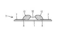
- FIG. 1is a top view of a substrate 1 used for manufacturing a first example of a transponder T 1 whose manufacturing process is illustrated in FIGS. 1 to 4 .
- the transponder T 1is depicted in FIGS. 4 and 7 .
- the substrate 1is made of polyethylene terephthalate (PET) and the top surface of the substrate 1 has a relatively high wettability so that it attracts a conductive adhesive relatively well, such as a conductive glue or a conductive solder, in the embodiment shown.
- a conductive adhesive relatively wellsuch as a conductive glue or a conductive solder
- soldermay be used alternatively for the embodiments of the invention.
- the substrate 1is first structured during a sputtering process.
- an area 2 having a relatively low wettabilityis formed on the top surface of the substrate 1 so that it repels the afore-mentioned conductive glue.
- further areas 3 and 4are created on the top surface of the substrate 1 .
- These areas 3 , 4are basically untreated, but are limited by small trenches 5 , 6 etched into the top surface of the substrate 1 in the embodiment shown. Consequently, areas 3 , 4 have a higher wettability than area 2 and even attract the afore-mentioned conductive glue.
- the area 2 with the low wettabilityis adjacent to and located between the areas 3 , 4 with the relatively high wettability.
- an antenna 7is formed on the top surface of the structured substrate 1 .
- the antenna 7has a first electric contact end 8 and a second electric contact end 9 , and the antenna 7 is plated on the top surface of the substrate 1 , using a well-known plating process.
- Each of the two antenna contact ends 8 , 9has an area 10 , 11 with a relatively high wettability so that they attract the afore-mentioned conductive glue (normally, the areas 10 , 11 coincide with the antenna contact ends 8 , 9 . However, this is not a mandatory feature of the invention).
- the area 10 of the first contact end 8borders the area 3 with the relatively high wettability and is spaced apart from the area 2 with the low wettability.
- the area 11 of the second contact end 9borders the area 4 with the relatively high wettability and is spaced apart from the area 2 with the relatively low wettability.
- an electric devicewhich is an integrated circuit 50 in this embodiment, is placed on the area 2 with the relatively low wettability.
- the integrated circuit 50is depicted in more detail in FIGS. 5 and 6 .
- the integrated circuit 50has the shape of a frustum of a pyramid and comprises a top surface 51 , a first side surface 52 , a second side surface 53 , a third side surface 54 , a fourth side surface 55 , and a bottom surface not shown in the Figures. Since the integrated circuit 50 has the shape of a frustum of a pyramid in this embodiment, the side surfaces 52 , 53 , 54 , 55 are inclined with respect to the bottom surface.
- the first side surface 52is arranged opposite the second side surface 54 .
- the first side surface 52comprises first electric contacts 56 and the third side surface 54 comprises second electric contacts 57 for electrically contacting the integrated circuit 50 .
- the integrated circuit 50is placed on the area 2 with the relatively low wettability in such a way that the first side surface 52 comprising the first electric contacts 56 faces the first antenna contact 8 , and the third side surface 54 comprising the second electric contacts 57 faces the second antenna contact 9 . Additionally, the bottom surface of the integrated circuit 50 is dimensioned in such a way that it partly overlaps the two areas 3 , 4 with the relatively high wettability when placed on the area 2 with the relatively low wettability, but without reaching the antenna contacts 8 , 9 .
- a conductive glue 12is applied on the areas 3 , 4 with the relatively high wettability and on the antenna contact ends 8 , 9 as shown in FIG. 4 . Since the area 2 of the substrate 1 has a relatively low wettability and the areas 3 , 4 of the substrate 1 as well as the areas 10 , 11 of the two antenna contact ends 8 , 9 have a relatively high wettability, substantially only the areas 3 , 4 , 10 , 11 are wetted by the conductive glue 12 .
- FIG. 7is a side view of the transponder T 1 .
- the conductive glue 12has a certain surface tension and a certain weight.
- the conductive glue 12thus substantially centers the integrated circuit 50 between the two antenna contacts 8 , 9 while being wet.
- the bottom surface of the integrated circuit 50partly covers the areas 3 , 4 with the relatively high wettability but does not reach the two antenna contact ends 10 , 11 of the antenna 7 .
- the integrated circuit 50is forced towards the substrate 1 because the surface tension and/or the weight of the conductive glue 12 acting on the inclined side walls 52 , 54 also result in a force component towards the substrate 1 .
- the integrated circuit 50 of the transponder T 1is shaped as a frustum of a pyramid, wherein its bottom surface is larger than its top surface 51 . Such an integrated circuit may also have a top surface which is larger than its bottom surface. Differently shaped integrated circuits may also be used.
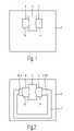
- An embodiment of a transponder T 2 having a differently shaped integrated circuit 80is shown in FIG. 8 .
- the integrated circuit 80has a rectangular shape.
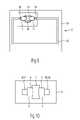
- FIG. 9shows a third embodiment of a transponder T 3 .
- Components of the transponder T 3 that are substantially identical to components of the transponder T 1 depicted in FIGS. 1 to 7have the same reference signs.
- the transponder T 3comprises an interposer substrate 91 and a main substrate 92 . Both substrates 91 and 92 are made of PET in the embodiment shown.
- the main substrate 92is provided with an antenna 93 formed by printing conductive ink on the top surface of the main substrate 92 .
- the antenna 93has a first contact end 94 and a second contact end 95 .
- the interposer substrate 91is shown in more detail in FIG. 10 and has a structure which is similar to that of the substrate 1 of the transponder T 1 .
- the interposer substrate 91thus has an area 2 with a relatively low wettability located between two areas 3 , 4 with a relatively high wettability.
- a first electric contact 98 and a second electric contact 99are formed on the top surface of the interposer substrate 91 , using a well-known plating process.
- Each of the two contacts 98 , 99has an area 110 , 111 with a relatively high wettability so that they attract a conductive glue (normally, the areas 110 , 111 coincide with the antenna contact ends 98 , 99 , which is, however, not a mandatory feature of the invention). Furthermore, the area 110 of the first electric contact 98 borders the area 3 with the relatively high wettability and is spaced apart from the area 2 with the low wettability. The area 111 of the second electric contact 99 borders the area 4 with the relatively high wettability and is spaced apart from the area 2 with the relatively low wettability.
- the integrated circuit 50is placed on the area 2 , and conductive glue 12 is applied to the areas 3 , 4 , 110 , 111 in order to electrically couple the integrated circuit 50 to the electric contacts 98 , 99 .
- the interposer substrate 91including the integrated circuit 50 , is then mounted on the main substrate 92 , and the first contact end 94 of the antenna 93 is electrically coupled to the first electric contact 98 of the interposer substrate 91 .
- the second contact end 95 of the antenna 93is electrically coupled to the second electric contact 99 of the interposer substrate 91 .
- the inventionapplies to transponders having a coil antenna, a dipole antenna, or a monopole antenna, as well as to a transponder having any other antenna.
- the inventionis not only applicable to transponders, but also to other electronic devices which are attached to a substrate and preferably have two connectors. Examples are LEDs (active parts), switches (electromechanical parts), resistors, capacitors, and coils (passive parts). It will be evident to those skilled in the art that this is not an exhaustive list, and many other alternatives can easily be found.
- the inventionalso relates to electronic devices having more than one or two connectors, e.g. an amplifier.
Landscapes
- Engineering & Computer Science (AREA)
- Microelectronics & Electronic Packaging (AREA)
- Computer Hardware Design (AREA)
- Physics & Mathematics (AREA)
- General Physics & Mathematics (AREA)
- Theoretical Computer Science (AREA)
- Manufacturing & Machinery (AREA)
- Details Of Aerials (AREA)
- Electric Connection Of Electric Components To Printed Circuits (AREA)
- Burglar Alarm Systems (AREA)
- Radar Systems Or Details Thereof (AREA)
Abstract
Description
Claims (17)
Applications Claiming Priority (4)
| Application Number | Priority Date | Filing Date | Title |
|---|---|---|---|
| EP05111387 | 2005-11-28 | ||
| EP05111387 | 2005-11-28 | ||
| EP05111387.6 | 2005-11-28 | ||
| PCT/IB2006/054407WO2007060630A1 (en) | 2005-11-28 | 2006-11-23 | Device comprising a substrate including an electric contact, and transponder |
Publications (2)
| Publication Number | Publication Date |
|---|---|
| US20080308310A1 US20080308310A1 (en) | 2008-12-18 |
| US8437141B2true US8437141B2 (en) | 2013-05-07 |
Family
ID=37890498
Family Applications (1)
| Application Number | Title | Priority Date | Filing Date |
|---|---|---|---|
| US12/095,138Expired - Fee RelatedUS8437141B2 (en) | 2005-11-28 | 2006-11-23 | Device comprising a substrate including an electronic contact, and transponder |
Country Status (7)
| Country | Link |
|---|---|
| US (1) | US8437141B2 (en) |
| EP (1) | EP1958133B1 (en) |
| JP (1) | JP2009517729A (en) |
| CN (1) | CN101317187B (en) |
| AT (1) | ATE500568T1 (en) |
| DE (1) | DE602006020484D1 (en) |
| WO (1) | WO2007060630A1 (en) |
Cited By (4)
| Publication number | Priority date | Publication date | Assignee | Title |
|---|---|---|---|---|
| US11393699B2 (en) | 2019-12-24 | 2022-07-19 | Vishay General Semiconductor, Llc | Packaging process for plating with selective molding |
| US11450534B2 (en) | 2019-12-24 | 2022-09-20 | Vishay General Semiconductor, Llc | Packaging process for side-wall plating with a conductive film |
| US12211704B2 (en) | 2019-03-08 | 2025-01-28 | Siliconix Incorporated | Semiconductor package having side wall plating |
| US12224232B2 (en) | 2019-03-08 | 2025-02-11 | Siliconix Incorporated | Semiconductor package having side wall plating |
Families Citing this family (4)
| Publication number | Priority date | Publication date | Assignee | Title |
|---|---|---|---|---|
| US20070102529A1 (en)* | 2005-11-08 | 2007-05-10 | Macsema, Inc. | Information devices |
| US20080106415A1 (en)* | 2006-11-08 | 2008-05-08 | Macsema, Inc. | Information tag |
| US9425500B2 (en)* | 2007-11-26 | 2016-08-23 | Nxp B.V. | Antenna or a strap for accommodating an integrated circuit, an antenna on a substrate, a strap for an integrated circuit and a transponder |
| EP3317821B1 (en)* | 2015-06-23 | 2019-07-17 | Linxens Holding | Smart card blank with at least one interface for contactless transmission of information |
Citations (14)
| Publication number | Priority date | Publication date | Assignee | Title |
|---|---|---|---|---|
| US4728751A (en)* | 1986-10-06 | 1988-03-01 | International Business Machines Corporation | Flexible electrical connection and method of making same |
| US5121298A (en)* | 1988-08-16 | 1992-06-09 | Delco Electronics Corporation | Controlled adhesion conductor |
| US6091332A (en) | 1998-06-09 | 2000-07-18 | Motorola, Inc. | Radio frequency identification tag having printed circuit interconnections |
| US6107920A (en) | 1998-06-09 | 2000-08-22 | Motorola, Inc. | Radio frequency identification tag having an article integrated antenna |
| US6172422B1 (en)* | 1996-07-11 | 2001-01-09 | Pfu Limited | Semiconductor device and a manufacturing method thereof |
| US20020038925A1 (en) | 2000-04-14 | 2002-04-04 | Karl Reimer | Apparatus and method for continuous surface modification of substrates |
| US6404643B1 (en) | 1998-10-15 | 2002-06-11 | Amerasia International Technology, Inc. | Article having an embedded electronic device, and method of making same |
| US6428189B1 (en)* | 2000-03-31 | 2002-08-06 | Relume Corporation | L.E.D. thermal management |
| US20020145197A1 (en)* | 2001-03-23 | 2002-10-10 | Ngk Spark Plug Co., Ltd. | Wiring substrate |
| US6665193B1 (en)* | 2002-07-09 | 2003-12-16 | Amerasia International Technology, Inc. | Electronic circuit construction, as for a wireless RF tag |
| US20040026754A1 (en)* | 2002-08-07 | 2004-02-12 | Peikang Liu | Radio frequency identification device and method |
| US6853087B2 (en) | 2000-09-19 | 2005-02-08 | Nanopierce Technologies, Inc. | Component and antennae assembly in radio frequency identification devices |
| US20050225222A1 (en)* | 2004-04-09 | 2005-10-13 | Joseph Mazzochette | Light emitting diode arrays with improved light extraction |
| US20070251339A1 (en)* | 2006-05-01 | 2007-11-01 | Sensarray Corporation | Process Condition Measuring Device with Shielding |
Family Cites Families (2)
| Publication number | Priority date | Publication date | Assignee | Title |
|---|---|---|---|---|
| US6891110B1 (en)* | 1999-03-24 | 2005-05-10 | Motorola, Inc. | Circuit chip connector and method of connecting a circuit chip |
| US6940408B2 (en)* | 2002-12-31 | 2005-09-06 | Avery Dennison Corporation | RFID device and method of forming |
- 2006
- 2006-11-23WOPCT/IB2006/054407patent/WO2007060630A1/enactiveApplication Filing
- 2006-11-23EPEP06831912Apatent/EP1958133B1/enactiveActive
- 2006-11-23CNCN200680044298.XApatent/CN101317187B/ennot_activeExpired - Fee Related
- 2006-11-23ATAT06831912Tpatent/ATE500568T1/ennot_activeIP Right Cessation
- 2006-11-23JPJP2008541891Apatent/JP2009517729A/ennot_activeWithdrawn
- 2006-11-23USUS12/095,138patent/US8437141B2/ennot_activeExpired - Fee Related
- 2006-11-23DEDE602006020484Tpatent/DE602006020484D1/enactiveActive
Patent Citations (15)
| Publication number | Priority date | Publication date | Assignee | Title |
|---|---|---|---|---|
| US4728751A (en)* | 1986-10-06 | 1988-03-01 | International Business Machines Corporation | Flexible electrical connection and method of making same |
| US5121298A (en)* | 1988-08-16 | 1992-06-09 | Delco Electronics Corporation | Controlled adhesion conductor |
| US6172422B1 (en)* | 1996-07-11 | 2001-01-09 | Pfu Limited | Semiconductor device and a manufacturing method thereof |
| US6091332A (en) | 1998-06-09 | 2000-07-18 | Motorola, Inc. | Radio frequency identification tag having printed circuit interconnections |
| US6107920A (en) | 1998-06-09 | 2000-08-22 | Motorola, Inc. | Radio frequency identification tag having an article integrated antenna |
| US6404643B1 (en) | 1998-10-15 | 2002-06-11 | Amerasia International Technology, Inc. | Article having an embedded electronic device, and method of making same |
| US6428189B1 (en)* | 2000-03-31 | 2002-08-06 | Relume Corporation | L.E.D. thermal management |
| US20020038925A1 (en) | 2000-04-14 | 2002-04-04 | Karl Reimer | Apparatus and method for continuous surface modification of substrates |
| US6853087B2 (en) | 2000-09-19 | 2005-02-08 | Nanopierce Technologies, Inc. | Component and antennae assembly in radio frequency identification devices |
| US20020145197A1 (en)* | 2001-03-23 | 2002-10-10 | Ngk Spark Plug Co., Ltd. | Wiring substrate |
| US6665193B1 (en)* | 2002-07-09 | 2003-12-16 | Amerasia International Technology, Inc. | Electronic circuit construction, as for a wireless RF tag |
| US20040026754A1 (en)* | 2002-08-07 | 2004-02-12 | Peikang Liu | Radio frequency identification device and method |
| US6867983B2 (en) | 2002-08-07 | 2005-03-15 | Avery Dennison Corporation | Radio frequency identification device and method |
| US20050225222A1 (en)* | 2004-04-09 | 2005-10-13 | Joseph Mazzochette | Light emitting diode arrays with improved light extraction |
| US20070251339A1 (en)* | 2006-05-01 | 2007-11-01 | Sensarray Corporation | Process Condition Measuring Device with Shielding |
Cited By (6)
| Publication number | Priority date | Publication date | Assignee | Title |
|---|---|---|---|---|
| US12211704B2 (en) | 2019-03-08 | 2025-01-28 | Siliconix Incorporated | Semiconductor package having side wall plating |
| US12224232B2 (en) | 2019-03-08 | 2025-02-11 | Siliconix Incorporated | Semiconductor package having side wall plating |
| US11393699B2 (en) | 2019-12-24 | 2022-07-19 | Vishay General Semiconductor, Llc | Packaging process for plating with selective molding |
| US11450534B2 (en) | 2019-12-24 | 2022-09-20 | Vishay General Semiconductor, Llc | Packaging process for side-wall plating with a conductive film |
| US11764075B2 (en) | 2019-12-24 | 2023-09-19 | Vishay General Semiconductor, Llc | Package assembly for plating with selective molding |
| US11876003B2 (en) | 2019-12-24 | 2024-01-16 | Vishay General Semiconductor, Llc | Semiconductor package and packaging process for side-wall plating with a conductive film |
Also Published As
| Publication number | Publication date |
|---|---|
| EP1958133B1 (en) | 2011-03-02 |
| CN101317187A (en) | 2008-12-03 |
| DE602006020484D1 (en) | 2011-04-14 |
| WO2007060630A1 (en) | 2007-05-31 |
| ATE500568T1 (en) | 2011-03-15 |
| US20080308310A1 (en) | 2008-12-18 |
| CN101317187B (en) | 2015-05-27 |
| JP2009517729A (en) | 2009-04-30 |
| EP1958133A1 (en) | 2008-08-20 |
Similar Documents
| Publication | Publication Date | Title |
|---|---|---|
| US8437141B2 (en) | Device comprising a substrate including an electronic contact, and transponder | |
| KR100770193B1 (en) | IC card | |
| US9779349B2 (en) | Method of producing a transponder and a transponder | |
| JP4855849B2 (en) | RFID tag manufacturing method and RFID tag | |
| JP2005129019A (en) | Ic card | |
| KR20010030032A (en) | Ic card | |
| CN101097611A (en) | RFID tag manufacturing method and RFID tag | |
| US20100243742A1 (en) | Rfid transponder | |
| US20160275391A1 (en) | Miniature rfid tag with coil on ic package | |
| US7960752B2 (en) | RFID tag | |
| US20090014527A1 (en) | Ask-026 | |
| JP2022507119A (en) | Electronic module for chip card | |
| EP2286446A1 (en) | Electronic device and method of manufacturing an electronic device | |
| US9661759B2 (en) | Printed circuit board and method of manufacturing the same | |
| JP2001035989A (en) | Method of forming an antenna circuit having an IC chip | |
| US7431218B2 (en) | RFID tag, module component, and RFID tag fabrication method | |
| JPH06344692A (en) | Thin module | |
| TWI379237B (en) | Rfid tag | |
| JP2001344575A (en) | Non-contact type ic card system | |
| KR20110054109A (en) | Stacked coil on chip and manufacturing method |
Legal Events
| Date | Code | Title | Description |
|---|---|---|---|
| AS | Assignment | Owner name:NXP B.V., NETHERLANDS Free format text:ASSIGNMENT OF ASSIGNORS INTEREST;ASSIGNORS:ROGY, REINHARD;ZENZ, CHRISTIAN;REEL/FRAME:021007/0207;SIGNING DATES FROM 20070911 TO 20070918 Owner name:NXP B.V., NETHERLANDS Free format text:ASSIGNMENT OF ASSIGNORS INTEREST;ASSIGNORS:ROGY, REINHARD;ZENZ, CHRISTIAN;SIGNING DATES FROM 20070911 TO 20070918;REEL/FRAME:021007/0207 | |
| STCF | Information on status: patent grant | Free format text:PATENTED CASE | |
| AS | Assignment | Owner name:MORGAN STANLEY SENIOR FUNDING, INC., MARYLAND Free format text:SECURITY AGREEMENT SUPPLEMENT;ASSIGNOR:NXP B.V.;REEL/FRAME:038017/0058 Effective date:20160218 | |
| AS | Assignment | Owner name:MORGAN STANLEY SENIOR FUNDING, INC., MARYLAND Free format text:CORRECTIVE ASSIGNMENT TO CORRECT THE REMOVE APPLICATION 12092129 PREVIOUSLY RECORDED ON REEL 038017 FRAME 0058. ASSIGNOR(S) HEREBY CONFIRMS THE SECURITY AGREEMENT SUPPLEMENT;ASSIGNOR:NXP B.V.;REEL/FRAME:039361/0212 Effective date:20160218 | |
| FPAY | Fee payment | Year of fee payment:4 | |
| AS | Assignment | Owner name:MORGAN STANLEY SENIOR FUNDING, INC., MARYLAND Free format text:CORRECTIVE ASSIGNMENT TO CORRECT THE REMOVE APPLICATION 12681366 PREVIOUSLY RECORDED ON REEL 039361 FRAME 0212. ASSIGNOR(S) HEREBY CONFIRMS THE SECURITY AGREEMENT SUPPLEMENT;ASSIGNOR:NXP B.V.;REEL/FRAME:042762/0145 Effective date:20160218 Owner name:MORGAN STANLEY SENIOR FUNDING, INC., MARYLAND Free format text:CORRECTIVE ASSIGNMENT TO CORRECT THE REMOVE APPLICATION 12681366 PREVIOUSLY RECORDED ON REEL 038017 FRAME 0058. ASSIGNOR(S) HEREBY CONFIRMS THE SECURITY AGREEMENT SUPPLEMENT;ASSIGNOR:NXP B.V.;REEL/FRAME:042985/0001 Effective date:20160218 | |
| AS | Assignment | Owner name:NXP B.V., NETHERLANDS Free format text:RELEASE BY SECURED PARTY;ASSIGNOR:MORGAN STANLEY SENIOR FUNDING, INC.;REEL/FRAME:050745/0001 Effective date:20190903 | |
| AS | Assignment | Owner name:MORGAN STANLEY SENIOR FUNDING, INC., MARYLAND Free format text:CORRECTIVE ASSIGNMENT TO CORRECT THE REMOVE APPLICATION 12298143 PREVIOUSLY RECORDED ON REEL 042762 FRAME 0145. ASSIGNOR(S) HEREBY CONFIRMS THE SECURITY AGREEMENT SUPPLEMENT;ASSIGNOR:NXP B.V.;REEL/FRAME:051145/0184 Effective date:20160218 Owner name:MORGAN STANLEY SENIOR FUNDING, INC., MARYLAND Free format text:CORRECTIVE ASSIGNMENT TO CORRECT THE REMOVE APPLICATION 12298143 PREVIOUSLY RECORDED ON REEL 039361 FRAME 0212. ASSIGNOR(S) HEREBY CONFIRMS THE SECURITY AGREEMENT SUPPLEMENT;ASSIGNOR:NXP B.V.;REEL/FRAME:051029/0387 Effective date:20160218 Owner name:MORGAN STANLEY SENIOR FUNDING, INC., MARYLAND Free format text:CORRECTIVE ASSIGNMENT TO CORRECT THE REMOVE APPLICATION 12298143 PREVIOUSLY RECORDED ON REEL 042985 FRAME 0001. ASSIGNOR(S) HEREBY CONFIRMS THE SECURITY AGREEMENT SUPPLEMENT;ASSIGNOR:NXP B.V.;REEL/FRAME:051029/0001 Effective date:20160218 Owner name:MORGAN STANLEY SENIOR FUNDING, INC., MARYLAND Free format text:CORRECTIVE ASSIGNMENT TO CORRECT THE REMOVE APPLICATION 12298143 PREVIOUSLY RECORDED ON REEL 038017 FRAME 0058. ASSIGNOR(S) HEREBY CONFIRMS THE SECURITY AGREEMENT SUPPLEMENT;ASSIGNOR:NXP B.V.;REEL/FRAME:051030/0001 Effective date:20160218 Owner name:MORGAN STANLEY SENIOR FUNDING, INC., MARYLAND Free format text:CORRECTIVE ASSIGNMENT TO CORRECT THE REMOVE APPLICATION12298143 PREVIOUSLY RECORDED ON REEL 039361 FRAME 0212. ASSIGNOR(S) HEREBY CONFIRMS THE SECURITY AGREEMENT SUPPLEMENT;ASSIGNOR:NXP B.V.;REEL/FRAME:051029/0387 Effective date:20160218 Owner name:MORGAN STANLEY SENIOR FUNDING, INC., MARYLAND Free format text:CORRECTIVE ASSIGNMENT TO CORRECT THE REMOVE APPLICATION12298143 PREVIOUSLY RECORDED ON REEL 042985 FRAME 0001. ASSIGNOR(S) HEREBY CONFIRMS THE SECURITY AGREEMENT SUPPLEMENT;ASSIGNOR:NXP B.V.;REEL/FRAME:051029/0001 Effective date:20160218 Owner name:MORGAN STANLEY SENIOR FUNDING, INC., MARYLAND Free format text:CORRECTIVE ASSIGNMENT TO CORRECT THE REMOVE APPLICATION12298143 PREVIOUSLY RECORDED ON REEL 042762 FRAME 0145. ASSIGNOR(S) HEREBY CONFIRMS THE SECURITY AGREEMENT SUPPLEMENT;ASSIGNOR:NXP B.V.;REEL/FRAME:051145/0184 Effective date:20160218 | |
| FEPP | Fee payment procedure | Free format text:MAINTENANCE FEE REMINDER MAILED (ORIGINAL EVENT CODE: REM.); ENTITY STATUS OF PATENT OWNER: LARGE ENTITY | |
| LAPS | Lapse for failure to pay maintenance fees | Free format text:PATENT EXPIRED FOR FAILURE TO PAY MAINTENANCE FEES (ORIGINAL EVENT CODE: EXP.); ENTITY STATUS OF PATENT OWNER: LARGE ENTITY | |
| STCH | Information on status: patent discontinuation | Free format text:PATENT EXPIRED DUE TO NONPAYMENT OF MAINTENANCE FEES UNDER 37 CFR 1.362 | |
| FP | Lapsed due to failure to pay maintenance fee | Effective date:20210507 |