US8436591B2 - Buck-boost converter with smooth transitions between modes - Google Patents
Buck-boost converter with smooth transitions between modesDownload PDFInfo
- Publication number
- US8436591B2 US8436591B2US12/546,602US54660209AUS8436591B2US 8436591 B2US8436591 B2US 8436591B2US 54660209 AUS54660209 AUS 54660209AUS 8436591 B2US8436591 B2US 8436591B2
- Authority
- US
- United States
- Prior art keywords
- buck
- boost
- switching transistor
- voltage
- mode
- Prior art date
- Legal status (The legal status is an assumption and is not a legal conclusion. Google has not performed a legal analysis and makes no representation as to the accuracy of the status listed.)
- Active, expires
Links
Images


Classifications
- H—ELECTRICITY
- H02—GENERATION; CONVERSION OR DISTRIBUTION OF ELECTRIC POWER
- H02M—APPARATUS FOR CONVERSION BETWEEN AC AND AC, BETWEEN AC AND DC, OR BETWEEN DC AND DC, AND FOR USE WITH MAINS OR SIMILAR POWER SUPPLY SYSTEMS; CONVERSION OF DC OR AC INPUT POWER INTO SURGE OUTPUT POWER; CONTROL OR REGULATION THEREOF
- H02M3/00—Conversion of DC power input into DC power output
- H02M3/02—Conversion of DC power input into DC power output without intermediate conversion into AC
- H02M3/04—Conversion of DC power input into DC power output without intermediate conversion into AC by static converters
- H02M3/10—Conversion of DC power input into DC power output without intermediate conversion into AC by static converters using discharge tubes with control electrode or semiconductor devices with control electrode
- H02M3/145—Conversion of DC power input into DC power output without intermediate conversion into AC by static converters using discharge tubes with control electrode or semiconductor devices with control electrode using devices of a triode or transistor type requiring continuous application of a control signal
- H02M3/155—Conversion of DC power input into DC power output without intermediate conversion into AC by static converters using discharge tubes with control electrode or semiconductor devices with control electrode using devices of a triode or transistor type requiring continuous application of a control signal using semiconductor devices only
- H02M3/156—Conversion of DC power input into DC power output without intermediate conversion into AC by static converters using discharge tubes with control electrode or semiconductor devices with control electrode using devices of a triode or transistor type requiring continuous application of a control signal using semiconductor devices only with automatic control of output voltage or current, e.g. switching regulators
- H02M3/158—Conversion of DC power input into DC power output without intermediate conversion into AC by static converters using discharge tubes with control electrode or semiconductor devices with control electrode using devices of a triode or transistor type requiring continuous application of a control signal using semiconductor devices only with automatic control of output voltage or current, e.g. switching regulators including plural semiconductor devices as final control devices for a single load
- H02M3/1582—Buck-boost converters
Definitions
- This inventionrelates to DC-DC voltage converters and, in particular, to a method for improved control over transitions between buck and boost modes of a DC-DC voltage converter.
- a buck-boost voltage converterreceives an unregulated input voltage and generates an increased or decreased regulated output voltage, where the target output voltage is set by component values in a feedback circuit.
- the buck-boost converters related to the present inventorare pulse-width modulation (PWM) converters, where the switching duty cycle of either buck or boost mode transistor switches controls the output voltage. The switching causes current through a smoothing inductor to ramp up and down as the inductor is charging and discharging.
- PWMpulse-width modulation
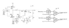
- FIG. 1is a simplified schematic diagram of the switching, feedback, and filtering components used by both a prior art PWM buck-boost converter and one embodiment of the inventive PWM buck-boost converter.
- a single inductor buck-boost converter 10typically consists of four switches arranged in a bridge configuration. Switches SW 1 and SW 2 form one pair, often referred to as the buck switches, while switches SW 3 and SW 4 form a second pair often referred to as the boost switches. Switch SW 2 is sometimes called a recirculating switch.
- Switches SW 1 and SW 2are mutually exclusive so, when switch SW 1 is on, switch SW 2 is off and vice versa. The same applies to switches SW 3 and SW 4 .
- Capacitor C 0filters the ramping inductor current and provides a relatively constant output voltage Vout.
- Capacitor C 1filters current signals generated by the error amplifier 12 and creates an error voltage Ve.
- the proportion of time for which switch SW 1 is closedis called the buck duty cycle and, similarly, the proportion of time for which switch SW 3 is closed is called the boost duty cycle.
- the duty cycles for the buck and boost switch pairsare controlled independently.
- the buck-boost converter 10controls the buck and the boost duty cycles in order to maintain a constant output voltage for a given input voltage Vin.
- the divided voltage between the resistors R 1 and R 2approximately equals the reference voltage Vref applied to the error amplifier 12 (a transconductance amplifier).
- the resistors R 3 and R 4set the gain of the error amplifier 12 .
- the filtered output of the error amplifier 12(the error voltage Ve) is compared to buck and boost sawtooth waveforms, and the time of crossing within the cycle controls the duty cycle of the buck or boost switches to maintain the output voltage Vout at the desired level.
- the sawtooth frequencyis typically greater than 1 MHz, the voltage feedback loop is a relatively slow loop since the output voltage is highly filtered and is slow to change.
- the comparatorsare part of a PWM controller (not shown in FIG. 1 ) that outputs pulses to buck and boost gate drivers 16 and 18 so that the proper switches are fully switched on and off and there is no overlap in the on-states.
- the buck-boost converter 10When the input voltage Vin is high, then the buck-boost converter 10 functions in buck mode, with switches SW 1 and SW 2 switching every cycle and with switch SW 4 permanently closed (and hence switch SW 3 permanently open).
- switch SW 1is on for a longer and longer proportion of each cycle, and switch SW 2 is on for less and less of each cycle.
- switch SW 1can no longer turn off fully at the end of each cycle (and switch SW 2 can no longer turn on fully) and, if nothing was done, the fixed frequency repetitive nature of the converter operation would be broken, and a series of pulses would ensue, where switch SW 1 would be on for 100% of some cycles and less than 100% for others.
- a buck-boost modeis a mode which is commonly used when the output voltage Vout is close to the input voltage Vin. In this mode, all four switches operate as two independently controlled pairs of mutually exclusive switches.
- switch SW 1In a pure boost mode, switch SW 1 is permanently on, and SW 2 is permanently off. As the input voltage Vin falls, then for a fixed output voltage, switch SW 3 comes on for longer proportions of the switching period (and hence SW 4 comes on less of the switching period).
- the boost modeIn a similar way to the buck mode, the boost mode is limited by the minimum time for which SW 3 can come on. If the input to output voltage ratio then demands a yet smaller time for SW 3 to come on, then a repetitive fixed frequency operation would be broken and SW 3 would be completely off for some periods and on for others, and the inductor current and output voltage ripple would undesirably increase.
- the rate of rise of inductor current in one cycleis related to the input voltage Vin minus the output voltage Vout, while the rate of decay of inductor current is proportional to the output voltage Vout.
- the inductor currentdecays to the same level at the end of a cycle as that level which started the cycle. This is shown in the graph 20 of FIG. 2 .
- the slopes of each inductor current waveform segmentare given in FIG. 2 , corresponding to a particular combination of switches being on.
- the voltage Vin across the inductorcorresponds to switches SW 1 and SW 3 being on.
- the voltage Vin-Vout across the inductorcorresponds to switches SW 1 and SW 4 being on.
- the voltage Vout across the inductorcorresponds to switches SW 2 and SW 4 being on.
- Graph 22shows the buck-boost mode that would result if we did nothing more than introduce a minimum boost pulse at the start of each buck-boost cycle when the converter just transitioned into the buck-boost mode.
- the buck modeAt the start of the buck-boost mode, when the input voltage has fallen to slightly greater than the output voltage, the buck mode continues to operate at its maximum duty cycle, so switch SW 2 turns on for a minimum time at the end of each cycle. Also, at the start of the buck-boost mode, the boost switch SW 3 turns on for the minimum time (in the minimum boost duty cycle).
- the inductor currentwill fall more rapidly, but rise more slowly (at least during the Vin-Vout portion). Eventually the inductor current will be able to fall to the same level at which it started the cycle, and stable buck-boost operation will be possible.
- Vin-Voutwill become negative and finally get to a point where we would want to remove the buck recirculation period (the Vout/L) period, to keep switch SW 2 off, and go to the boost mode.
- the inventionis an improved method to control buck and boost duty cycles for more stable transitions into and out of a buck-boost mode.
- the methodologyis realizable in a practical converter for ensuring that, regardless of the input and output voltages, there is always a stable operating point that maintains the inductor current ripple and output voltage ripple at the switching frequency, causing the ripple to be the smallest realizable value.
- the conventional switching hardware of a buck-boost converteris used, but the PWM controller logic that controls the buck-boost mode is modified so that, as the converter enters the buck-boost mode from the buck mode (i.e., the boost duty cycle begins at a minimum), the buck mode duty cycle is not kept at maximum (in contrast to the prior art) but the switch SW 2 (the recirculating switch) on-time is immediately increased (buck duty cycle is decreased) by the length of the boost mode switch SW 3 minimum on time. This offsets the effect of the boost mode switch SW 3 being on longer than is needed for regulation, so the transition between the buck mode and the buck-boost mode approximates the ideal transition.
- the extended on-time of the switch SW 2causes the inductor current to fall by about the same as the boost switch SW 3 minimum on-time caused the inductor current to rise. Therefore, the inductor current at the beginning of a switching cycle will be about the same as at the end of the switching cycle, and stability is achieved.
- the converterWhen the switch SW 2 on-time is reduced to its minimum on-time, yet the input voltage keeps falling, the converter enters the boost mode.
- the recirculation pulse that turns on the switch SW 2is stopped, and the on-time of the boost switch SW 3 is immediately reduced by the same amount as the minimum on-time of switch SW 2 , so that the inductor current at the start of a cycle is the same as at the end of the cycle.
- the converterwill maintain switch SW 2 off and maintain switch SW 1 on and only operate the boost switches SW 3 and SW 4 .
- the circuitry to offset the on-time of switches (i.e., vary lengths of on and off pulses) to compensate switching during the buck-boost modeis simple.
- the error voltage (or other control voltage) applied to buck and boost ramping waveformsis separately offset by an amount depending on the level of the error voltage.
- the error voltagedetermines the mode and duty cycle (after any offsets) of the converter.
- the on-time and off-time of the switchesis compensated by shifting the buck and boost ramps up or down. Other techniques may also be used, such as delays.
- FIG. 1is a simplified schematic diagram of the switching, feedback, and filtering components used by both a prior art PWM buck-boost converter and the inventive PWM buck-boost converter.
- FIG. 2illustrates the prior art buck and buck-boost inductor current waveforms near the transition between the two modes, showing how oscillations between the buck-boost mode and buck mode will arise due to the inability of the buck mode to achieve near a full 100% duty cycle (switch SW 2 has a fixed minimum on-time) and the inability of the boost mode to achieve near a 0% duty cycle (switch SW 3 has a fixed minimum on-time).
- FIG. 3illustrates offset buck and boost ramping waveforms and the control voltage levels that control the switching times of the switches.
- FIG. 4illustrates a technique for individually offsetting the buck and boost ramping waveforms to compensate for the buck and boost duty cycles not being able to smoothly vary between 0%-100% duty cycles.
- FIG. 5illustrates pulses to each of the switches in FIG. 1 near the transition into and out of the buck-boost mode to compensate for the buck and boost duty cycles not being able to smoothly vary between 0%-100% duty cycles.
- FIG. 6illustrates the buck and buck-boost inductor current waveforms near the transition between the two modes achieved by the inventive converter, where the inductor current at the beginning of a switching cycle is the same as the inductor current at the end of the cycle.
- FIG. 7illustrates one type of technique for individually offsetting the control voltages applied to the buck and boost ramping waveforms to compensate for the buck and boost duty cycles not being able to smoothly vary between 0%-100% duty cycles.
- FIG. 1The circuitry of FIG. 1 , in combination with the PWM control circuitry described with respect to FIGS. 3-7 , creates a converter in accordance with one embodiment of the invention.
- FIGS. 3-5will be summarily described followed by a more detailed description.
- FIG. 3illustrates a buck ramp waveform 28 and a boost ramp waveform 30 .
- the ramp waveforms 28 and 30have the same frequency (typically greater than 1 MHz) but have a DC offset so that they cross a control voltage at different times.
- the crossing timescontrol the duty cycles of the switches SW 1 -SW 4 in FIG. 1 , where the switching of switches SW 1 and SW 2 are mutually exclusive, and the switching of switches SW 3 and SW 4 are mutually exclusive.
- Generating ramping waveformsis conventional in a voltage converter. Generating ramping waveforms and comparing the waveforms to an error voltage for controlling converter switches are described in detail in U.S. Pat. No. 7,432,689, by Ira Miller et al., assigned to the present assignee and incorporated herein by reference.
- FIG. 4illustrates a PWM controller 32 that receives the ramp waveforms 28 and 30 and the conventional error voltage or other control voltage Vc and variably offsets the ramp waveforms 28 and 30 during the buck-boost mode of the converter to compensate for the buck and boost duty cycles not being able to smoothly vary between 0%-100% duty cycles.
- the PWM controller 32outputs pulses to the buck and boost drivers 16 and 18 ( FIG. 1 ) to control the duty cycles of the switches SW 1 -SW 4 , and examples of logic pulses to the gates of the various MOSFET switches SW 1 -SW 4 are represented in FIG. 5 near the buck-boost transition.
- control voltages 34 , 35 , and 36are shown as control voltages 34 , 35 , and 36 .
- These control voltages 34 - 36may be the conventional error voltage Ve in FIG. 1 or may be a demand signal in a current controlled loop.
- the level of the control signaldetermines the mode of the converter and the duty cycles of the various switches SW 1 -SW 4 .
- the buck ramp waveform 28 and boost ramp waveform 30are shown overlapping so that both the buck and boost switches are switched each cycle.
- the error voltage VeWhen the input voltage Vin ( FIG. 1 ) is significantly higher than the output voltage, the error voltage Ve will cause the demand signal to be low in order to keep the feedback voltage Vfb equal to Vref, and this will result in a lower overall average voltage demand across the inductor.
- An example of such a low demand signalis control voltage 34 ( FIG. 3 ), which only intersects the buck ramp waveform 28 during some portion of the cycle. So, the converter will operate in the buck mode.
- the control voltage (Vc)is compared to the boost and buck ramp waveforms by a boost PWM comparator 1 and a buck PWM comparator 2 .
- the outputs of the comparatorsare applied to the boost and buck drivers 18 and 16 in FIG. 1 .
- the boost switch SW 4will remain on, and the boost switch SW 3 will remain off during the buck mode. From time T 0 to time Ta, the buck switch SW 1 is on and switch SW 2 is off. Between time Ta and T 1 , switch SW 2 is on and switch SW 1 is off.
- control voltage 36( FIG. 3 ), which only intersects the boost ramp waveform 30 during some portion of the cycle. So, the converter will operate in the boost mode.
- the control signalmay represent an error voltage in a voltage loop or a current error in a current loop.
- the buck switch SW 1will remain on, and the buck switch SW 2 will remain off during the boost mode. From time T 0 to time Tb, the boost switch SW 3 is on and switch SW 4 is off. Between time Tb and T 1 , switch SW 4 is on and switch SW 3 is off.
- the duty cycles of the buck or boost transistorswill change to maintain the output voltage Vout at the regulated level. If the power supply is a battery, the control voltage increases as the battery voltage goes down, for a constant output voltage.
- the converteroperates in the buck-boost mode.
- the switch control pulses of FIG. 5are compensated by variable offsets of the ramps, shown in FIG. 4 , to compensate for minimum pulse on-times/off-times near the transitions into and out of the buck-boost mode.
- the graph set 40 in FIG. 5identifies the on and off times for the various switches SW 1 -SW 4 when the input voltage Vin has dropped to slightly higher than the output voltage so that the buck mode is operating at its maximum duty cycle. Since there is a minimum on-time of the switch SW 2 , the duty cycle is somewhat less than 100%, such as between 90%-95%. At this time, just prior to entering the buck-boost mode, the buck switch SW 2 is on for its minimum on-time at the end of the cycle, the buck switch SW 1 is off for its minimum off-time, the boost mode switch SW 4 is maintained on, and the boost mode switch SW 3 is maintained off. Since SW 1 and SW 2 are mutually exclusive and SW 3 and SW 4 are mutually exclusive, the status of all switches does not need to be identified for simplicity.
- the graph set 42 in FIG. 5represents the on and off times for the various switches SW 1 -SW 4 when the converter has just entered the buck-boost mode from the buck mode.
- the ideal boost duty cyclewill be slightly higher than 0%.
- the minimum duty cycle of the boost switch SW 3is realistically greater than 5%, so the on-time of the switch SW 3 is the minimum pulse shown in the graph set 42 . This on-time of the switch SW 3 is more than needed to keep the output voltage at its regulated level, as discussed with respect to FIG. 2 .
- the on-time of the buck switch SW 2is immediately increased by about the minimum on-time of switch SW 3 to create a widened on-time pulse for switch SW 2 . Therefore, instead of the buck switches being at the maximum duty cycle at the start of the buck-boost mode, as done in the prior art, the buck duty cycle is reduced. This instant reduction in the buck duty cycle may be accomplished by offsetting the buck ramp waveform 28 upward at the time that the control voltage is high enough to begin crossing the boost ramp waveform 30 , or by other means such as offsetting the demand signal during this region of operation. Such a variable offset circuit 44 is shown in FIG. 4 .
- Such a variable offsetmay be created by sensing when the control voltage has exceeded a certain level and then level shifting the buck ramp waveform 28 by a certain amount to offset the minimum on-time of the switch SW 3 .
- offset demand signalsmight be used, and appropriate comparators selected during this region of operation.
- the offsettingmaintains the output voltage at its regulated level and causes the inductor current at the beginning of a cycle to be the same as at the end of the cycle, as shown in the graphs 45 and 46 of FIG. 6 , where graph 45 illustrates the inductor current waveform just before entering the buck-boost mode, and graph 46 illustrates the inductor current waveform just after entering the buck-boost mode.
- the buck duty cycleincreases in order to maintain the regulated output voltage and to cause the inductor current at the beginning of a cycle to be the same as at the end of the cycle, as shown in the graphs of FIG. 6 .
- the input voltagewill have sufficiently fallen so that the buck-boost mode will be about to transition to the boost mode.
- Graph set 48illustrates the switching signals prior to entering the boost mode.
- the buck modeis back at its maximum duty cycle (minimum switch SW 2 on-time), while the boost mode is at a duty cycle somewhat greater than its minimum duty cycle (switch SW 3 on longer than minimum on-time) to keep the output voltage at the regulated voltage.
- the boost ramp waveform 30is immediately returned by being offset upward upon transitioning into the boost mode to reduce the switch SW 3 on-time by an amount that compensates for the buck switch SW 2 remaining open in the boost mode.
- the drop in the switch SW 3 on-timewill be about the same as the switch SW 2 minimum on-time just prior to entering the boost mode.
- the boost ramp waveform variable offset circuitry 52is shown in FIG. 4 .
- the resultis a smooth transition into and out of the buck-boost mode without oscillating between modes, so as to achieve a minimum ripple in the output voltage.
- the variable offsetting of the ramp waveformscauses the inductor current at the beginning of a cycle to be about the same as at the end of a cycle.
- the offsetting of the boost ramp waveform 30 and buck waveform 28would follow in reverse to that described above, where the boost ramp waveform 30 would be immediately shifted down to increase the boost duty cycle to offset the minimum on-time of the buck switch SW 2 when the converter entered the buck-boost mode.
- the duty cycle of the boost switchesdecreases to the minimum while the duty cycle of the buck switches increases.
- the buck ramp waveform 28is immediately offset downward to compensate for the boost switch SW 3 remaining off.
- the circuitry for level shifting the ramps (or offsetting the demand signal) in response to the level of the control signalis very simple and may be done in many different ways, including digitally. Variable level shifting is common in certain applications, and various level shifting techniques are well known.
- the control signalitself may be variably offset, which is equivalent to shifting the ramps since the signal levels are compared. For example, shifting the control signal up for comparison to the boost ramp waveform is equivalent to shifting the boost ramp waveform down.
- FIG. 7illustrates a PWM controller 56 that variably offsets the error voltage or other control voltage by variable offset circuits 58 and 60 , depending on the levels of the control voltage Vc, to achieve the same results as shown in FIG. 5 .
- the offsetting for compensationwould be greater than that needed in an ideal converter. Primarily this is to overcome offsets and other non-idealities that may otherwise result in poor operation and transient oscillation around the buck to buck-boost or buck-boost to boost thresholds.
- the optimum offsetsare determined by the particular application.
- a level of hysteresismay be added to the levels at which the buck-boost mode is entered and exited by using hysteresis comparators in the PWM controller circuit.
Landscapes
- Engineering & Computer Science (AREA)
- Power Engineering (AREA)
- Dc-Dc Converters (AREA)
Abstract
Description
Claims (7)
Priority Applications (2)
| Application Number | Priority Date | Filing Date | Title |
|---|---|---|---|
| US12/546,602US8436591B2 (en) | 2009-08-24 | 2009-08-24 | Buck-boost converter with smooth transitions between modes |
| US13/277,559US8773084B2 (en) | 2009-08-24 | 2011-10-20 | Buck-boost converter using timers for mode transition control |
Applications Claiming Priority (1)
| Application Number | Priority Date | Filing Date | Title |
|---|---|---|---|
| US12/546,602US8436591B2 (en) | 2009-08-24 | 2009-08-24 | Buck-boost converter with smooth transitions between modes |
Related Child Applications (1)
| Application Number | Title | Priority Date | Filing Date |
|---|---|---|---|
| US13/277,559Continuation-In-PartUS8773084B2 (en) | 2009-08-24 | 2011-10-20 | Buck-boost converter using timers for mode transition control |
Publications (2)
| Publication Number | Publication Date |
|---|---|
| US20110043172A1 US20110043172A1 (en) | 2011-02-24 |
| US8436591B2true US8436591B2 (en) | 2013-05-07 |
Family
ID=43604815
Family Applications (1)
| Application Number | Title | Priority Date | Filing Date |
|---|---|---|---|
| US12/546,602Active2031-07-26US8436591B2 (en) | 2009-08-24 | 2009-08-24 | Buck-boost converter with smooth transitions between modes |
Country Status (1)
| Country | Link |
|---|---|
| US (1) | US8436591B2 (en) |
Cited By (10)
| Publication number | Priority date | Publication date | Assignee | Title |
|---|---|---|---|---|
| US20110241636A1 (en)* | 2010-01-29 | 2011-10-06 | Intersil Americas Inc. | Multi-phase non-inverting buck boost voltage converter |
| US20130264870A1 (en)* | 2012-04-10 | 2013-10-10 | Sol Chip Ltd. | Integrated circuit energy harvester |
| US9647546B2 (en) | 2013-12-05 | 2017-05-09 | Fairchild Semiconductor Corporation | Dual-mode voltage doubling buck converter with smooth mode transition |
| US9973083B1 (en) | 2016-11-15 | 2018-05-15 | Nxp B.V. | DC-DC converter controller |
| US10594218B1 (en) | 2017-12-20 | 2020-03-17 | Renesas Electronics America Inc. | Hysteresis timing scheme for mode transition in a buck boost converter |
| US10637357B1 (en) | 2017-12-20 | 2020-04-28 | Renesas Electronics America Inc. | Ramp offset compensation circuit in a buck boost converter |
| US11303212B2 (en) | 2014-12-05 | 2022-04-12 | Analog Devices International Unlimited Company | Peak-buck peak-boost current-mode control for switched step-up step-down regulators |
| US11682972B2 (en) | 2021-02-04 | 2023-06-20 | Analog Devices, Inc. | Peak current mode control for buck-boost regulators |
| US12273032B2 (en) | 2021-11-15 | 2025-04-08 | Samsung Electronics Co., Ltd. | Charger integrated circuit including bidirectional switching converter, and electronic device including the charger integrated circuit |
| US12374995B2 (en) | 2022-01-14 | 2025-07-29 | Samsung Electronics Co., Ltd. | Charging integrated circuit including bidirectional switching converter, and electronic device including the same |
Families Citing this family (81)
| Publication number | Priority date | Publication date | Assignee | Title |
|---|---|---|---|---|
| US10693415B2 (en) | 2007-12-05 | 2020-06-23 | Solaredge Technologies Ltd. | Testing of a photovoltaic panel |
| US11881814B2 (en) | 2005-12-05 | 2024-01-23 | Solaredge Technologies Ltd. | Testing of a photovoltaic panel |
| US8319483B2 (en) | 2007-08-06 | 2012-11-27 | Solaredge Technologies Ltd. | Digital average input current control in power converter |
| US11569659B2 (en) | 2006-12-06 | 2023-01-31 | Solaredge Technologies Ltd. | Distributed power harvesting systems using DC power sources |
| US11735910B2 (en) | 2006-12-06 | 2023-08-22 | Solaredge Technologies Ltd. | Distributed power system using direct current power sources |
| US12316274B2 (en) | 2006-12-06 | 2025-05-27 | Solaredge Technologies Ltd. | Pairing of components in a direct current distributed power generation system |
| US8384243B2 (en) | 2007-12-04 | 2013-02-26 | Solaredge Technologies Ltd. | Distributed power harvesting systems using DC power sources |
| US11296650B2 (en) | 2006-12-06 | 2022-04-05 | Solaredge Technologies Ltd. | System and method for protection during inverter shutdown in distributed power installations |
| US8618692B2 (en) | 2007-12-04 | 2013-12-31 | Solaredge Technologies Ltd. | Distributed power system using direct current power sources |
| US11888387B2 (en) | 2006-12-06 | 2024-01-30 | Solaredge Technologies Ltd. | Safety mechanisms, wake up and shutdown methods in distributed power installations |
| US11309832B2 (en) | 2006-12-06 | 2022-04-19 | Solaredge Technologies Ltd. | Distributed power harvesting systems using DC power sources |
| US11855231B2 (en) | 2006-12-06 | 2023-12-26 | Solaredge Technologies Ltd. | Distributed power harvesting systems using DC power sources |
| US8319471B2 (en) | 2006-12-06 | 2012-11-27 | Solaredge, Ltd. | Battery power delivery module |
| US9088178B2 (en) | 2006-12-06 | 2015-07-21 | Solaredge Technologies Ltd | Distributed power harvesting systems using DC power sources |
| US8013472B2 (en) | 2006-12-06 | 2011-09-06 | Solaredge, Ltd. | Method for distributed power harvesting using DC power sources |
| US11687112B2 (en) | 2006-12-06 | 2023-06-27 | Solaredge Technologies Ltd. | Distributed power harvesting systems using DC power sources |
| US8816535B2 (en) | 2007-10-10 | 2014-08-26 | Solaredge Technologies, Ltd. | System and method for protection during inverter shutdown in distributed power installations |
| US8473250B2 (en) | 2006-12-06 | 2013-06-25 | Solaredge, Ltd. | Monitoring of distributed power harvesting systems using DC power sources |
| US9130401B2 (en) | 2006-12-06 | 2015-09-08 | Solaredge Technologies Ltd. | Distributed power harvesting systems using DC power sources |
| US8963369B2 (en) | 2007-12-04 | 2015-02-24 | Solaredge Technologies Ltd. | Distributed power harvesting systems using DC power sources |
| US8947194B2 (en) | 2009-05-26 | 2015-02-03 | Solaredge Technologies Ltd. | Theft detection and prevention in a power generation system |
| US9112379B2 (en) | 2006-12-06 | 2015-08-18 | Solaredge Technologies Ltd. | Pairing of components in a direct current distributed power generation system |
| CN105244905B (en) | 2007-12-05 | 2019-05-21 | 太阳能安吉有限公司 | Release mechanism in distributed power device is waken up and method for closing |
| EP2225778B1 (en) | 2007-12-05 | 2019-06-26 | Solaredge Technologies Ltd. | Testing of a photovoltaic panel |
| US11264947B2 (en) | 2007-12-05 | 2022-03-01 | Solaredge Technologies Ltd. | Testing of a photovoltaic panel |
| WO2009073867A1 (en) | 2007-12-05 | 2009-06-11 | Solaredge, Ltd. | Parallel connected inverters |
| WO2009072076A2 (en) | 2007-12-05 | 2009-06-11 | Solaredge Technologies Ltd. | Current sensing on a mosfet |
| US9291696B2 (en) | 2007-12-05 | 2016-03-22 | Solaredge Technologies Ltd. | Photovoltaic system power tracking method |
| US8111052B2 (en) | 2008-03-24 | 2012-02-07 | Solaredge Technologies Ltd. | Zero voltage switching |
| EP2294669B8 (en) | 2008-05-05 | 2016-12-07 | Solaredge Technologies Ltd. | Direct current power combiner |
| EP2602831B1 (en) | 2009-05-22 | 2014-07-16 | Solaredge Technologies Ltd. | Electrically isolated heat dissipating junction box |
| US8773084B2 (en)* | 2009-08-24 | 2014-07-08 | Micrel, Inc. | Buck-boost converter using timers for mode transition control |
| US12418177B2 (en) | 2009-10-24 | 2025-09-16 | Solaredge Technologies Ltd. | Distributed power system using direct current power sources |
| US8710699B2 (en) | 2009-12-01 | 2014-04-29 | Solaredge Technologies Ltd. | Dual use photovoltaic system |
| US8766696B2 (en) | 2010-01-27 | 2014-07-01 | Solaredge Technologies Ltd. | Fast voltage level shifter circuit |
| US8912779B2 (en)* | 2010-04-19 | 2014-12-16 | Linear Technology Corporation | Switching scheme for step up-step down converters using fixed frequency current-mode control |
| US8963528B2 (en) | 2010-04-30 | 2015-02-24 | Lockheed Martin Corporation | Method and means to implement fixed frequency operation of buck mode switching |
| US8547141B2 (en) | 2010-04-30 | 2013-10-01 | Lockheed Martin Corporation | Wide dynamic range, wide bandwidth, voltage to current converter |
| US8564271B2 (en) | 2010-06-01 | 2013-10-22 | Lockheed Martin Corporation | Method and means to implement a current follower operation of a buck mode, switching power supply |
| US9110480B2 (en)* | 2010-06-09 | 2015-08-18 | Infineon Technologies Austria Ag | Voltage ramp circuitry and voltage ramp methods for voltage regulators |
| GB2485527B (en) | 2010-11-09 | 2012-12-19 | Solaredge Technologies Ltd | Arc detection and prevention in a power generation system |
| US10230310B2 (en) | 2016-04-05 | 2019-03-12 | Solaredge Technologies Ltd | Safety switch for photovoltaic systems |
| US10673229B2 (en) | 2010-11-09 | 2020-06-02 | Solaredge Technologies Ltd. | Arc detection and prevention in a power generation system |
| US10673222B2 (en) | 2010-11-09 | 2020-06-02 | Solaredge Technologies Ltd. | Arc detection and prevention in a power generation system |
| GB2486408A (en) | 2010-12-09 | 2012-06-20 | Solaredge Technologies Ltd | Disconnection of a string carrying direct current |
| GB2483317B (en) | 2011-01-12 | 2012-08-22 | Solaredge Technologies Ltd | Serially connected inverters |
| US8736245B1 (en) | 2011-01-20 | 2014-05-27 | Lockheed Martin Corporation | Method and means to combine pulse width modulation level control, full resonance and zero voltage switching for switched mode power supplies |
| US8570005B2 (en) | 2011-09-12 | 2013-10-29 | Solaredge Technologies Ltd. | Direct current link circuit |
| GB2498365A (en) | 2012-01-11 | 2013-07-17 | Solaredge Technologies Ltd | Photovoltaic module |
| GB2498790A (en) | 2012-01-30 | 2013-07-31 | Solaredge Technologies Ltd | Maximising power in a photovoltaic distributed power system |
| US9853565B2 (en) | 2012-01-30 | 2017-12-26 | Solaredge Technologies Ltd. | Maximized power in a photovoltaic distributed power system |
| GB2498791A (en) | 2012-01-30 | 2013-07-31 | Solaredge Technologies Ltd | Photovoltaic panel circuitry |
| GB2499991A (en) | 2012-03-05 | 2013-09-11 | Solaredge Technologies Ltd | DC link circuit for photovoltaic array |
| EP3499695B1 (en) | 2012-05-25 | 2024-09-18 | Solaredge Technologies Ltd. | Circuit for interconnected direct current power sources |
| US10115841B2 (en) | 2012-06-04 | 2018-10-30 | Solaredge Technologies Ltd. | Integrated photovoltaic panel circuitry |
| US9800158B2 (en) | 2013-01-30 | 2017-10-24 | Nvidia Corporation | Current-parking switching regulator downstream controller |
| US9804621B2 (en)* | 2013-02-05 | 2017-10-31 | Nvidia Corporation | Current-parking switching regulator downstream controller pre-driver |
| US9639102B2 (en) | 2013-02-19 | 2017-05-02 | Nvidia Corporation | Predictive current sensing |
| US9941813B2 (en) | 2013-03-14 | 2018-04-10 | Solaredge Technologies Ltd. | High frequency multi-level inverter |
| US9548619B2 (en) | 2013-03-14 | 2017-01-17 | Solaredge Technologies Ltd. | Method and apparatus for storing and depleting energy |
| EP3506370B1 (en) | 2013-03-15 | 2023-12-20 | Solaredge Technologies Ltd. | Bypass mechanism |
| EP2779398B1 (en) | 2013-03-15 | 2019-01-23 | Dialog Semiconductor GmbH | A control method of high efficient buck-boost switching regulator |
| US20140312868A1 (en)* | 2013-04-23 | 2014-10-23 | Nvidia Corporation | Control of a soft-switched variable frequency multi-phase regulator |
| US9231477B2 (en) | 2013-04-23 | 2016-01-05 | Nvidia Corporation | Control of a soft-switched variable frequency buck regulator |
| CN103715886B (en)* | 2013-12-11 | 2017-01-11 | 矽力杰半导体技术(杭州)有限公司 | Four-switch buck/boost mode converter control method and control circuit |
| US9318974B2 (en) | 2014-03-26 | 2016-04-19 | Solaredge Technologies Ltd. | Multi-level inverter with flying capacitor topology |
| US10476372B2 (en)* | 2014-12-22 | 2019-11-12 | Futurewei Technologies, Inc. | Buck-boost power converter and method of operation thereof |
| DE102015223768B4 (en) | 2015-11-30 | 2019-10-31 | Dialog Semiconductor (Uk) Limited | Buck-boost converter |
| JP6594199B2 (en)* | 2015-12-28 | 2019-10-23 | ローム株式会社 | Switching regulator |
| CN107153212B (en) | 2016-03-03 | 2023-07-28 | 太阳能安吉科技有限公司 | Method for mapping a power generation facility |
| US10599113B2 (en) | 2016-03-03 | 2020-03-24 | Solaredge Technologies Ltd. | Apparatus and method for determining an order of power devices in power generation systems |
| US11081608B2 (en) | 2016-03-03 | 2021-08-03 | Solaredge Technologies Ltd. | Apparatus and method for determining an order of power devices in power generation systems |
| US10224813B2 (en) | 2016-03-24 | 2019-03-05 | Nvidia Corporation | Variable frequency soft-switching control of a buck converter |
| US11018623B2 (en) | 2016-04-05 | 2021-05-25 | Solaredge Technologies Ltd. | Safety switch for photovoltaic systems |
| US12057807B2 (en) | 2016-04-05 | 2024-08-06 | Solaredge Technologies Ltd. | Chain of power devices |
| US11177663B2 (en) | 2016-04-05 | 2021-11-16 | Solaredge Technologies Ltd. | Chain of power devices |
| US9973090B1 (en)* | 2016-10-20 | 2018-05-15 | Silicon Mitus, Inc. | Buck boost converter and control method thereof |
| US10128757B2 (en) | 2017-03-03 | 2018-11-13 | Dialog Semiconductor (Uk) Limited | Buck-boost converter with small disturbance at mode transitions |
| CN111884513B (en) | 2018-07-09 | 2021-12-03 | 华为数字能源技术有限公司 | Control circuit applied to power adapter and power adapter |
| IT201900014715A1 (en)* | 2019-08-13 | 2021-02-13 | St Microelectronics Srl | CONTROL DEVICE FOR SWITCHING VOLTAGE REGULATOR AND CONTROL METHOD |
| CN113472199B (en)* | 2021-06-30 | 2022-09-27 | 易事特集团股份有限公司 | Mode smooth switching method and system of Buck-Boost circuit |
Citations (2)
| Publication number | Priority date | Publication date | Assignee | Title |
|---|---|---|---|---|
| US7432689B2 (en) | 2006-05-05 | 2008-10-07 | Micrel, Inc. | Buck-boost control logic for PWM regulator |
| US20090045786A1 (en)* | 2007-08-14 | 2009-02-19 | Freescale Semiconductor, Inc. | Mode transitioning in a dc/dc converter using a constant duty cycle difference |
- 2009
- 2009-08-24USUS12/546,602patent/US8436591B2/enactiveActive
Patent Citations (2)
| Publication number | Priority date | Publication date | Assignee | Title |
|---|---|---|---|---|
| US7432689B2 (en) | 2006-05-05 | 2008-10-07 | Micrel, Inc. | Buck-boost control logic for PWM regulator |
| US20090045786A1 (en)* | 2007-08-14 | 2009-02-19 | Freescale Semiconductor, Inc. | Mode transitioning in a dc/dc converter using a constant duty cycle difference |
Cited By (12)
| Publication number | Priority date | Publication date | Assignee | Title |
|---|---|---|---|---|
| US20110241636A1 (en)* | 2010-01-29 | 2011-10-06 | Intersil Americas Inc. | Multi-phase non-inverting buck boost voltage converter |
| US8896279B2 (en)* | 2010-01-29 | 2014-11-25 | Intersil Americals LLC | Multi-phase non-inverting buck boost voltage converter |
| US20130264870A1 (en)* | 2012-04-10 | 2013-10-10 | Sol Chip Ltd. | Integrated circuit energy harvester |
| US9379543B2 (en)* | 2012-04-10 | 2016-06-28 | Sol Chip Ltd. | Integrated circuit energy harvester |
| US9647546B2 (en) | 2013-12-05 | 2017-05-09 | Fairchild Semiconductor Corporation | Dual-mode voltage doubling buck converter with smooth mode transition |
| US11303212B2 (en) | 2014-12-05 | 2022-04-12 | Analog Devices International Unlimited Company | Peak-buck peak-boost current-mode control for switched step-up step-down regulators |
| US9973083B1 (en) | 2016-11-15 | 2018-05-15 | Nxp B.V. | DC-DC converter controller |
| US10594218B1 (en) | 2017-12-20 | 2020-03-17 | Renesas Electronics America Inc. | Hysteresis timing scheme for mode transition in a buck boost converter |
| US10637357B1 (en) | 2017-12-20 | 2020-04-28 | Renesas Electronics America Inc. | Ramp offset compensation circuit in a buck boost converter |
| US11682972B2 (en) | 2021-02-04 | 2023-06-20 | Analog Devices, Inc. | Peak current mode control for buck-boost regulators |
| US12273032B2 (en) | 2021-11-15 | 2025-04-08 | Samsung Electronics Co., Ltd. | Charger integrated circuit including bidirectional switching converter, and electronic device including the charger integrated circuit |
| US12374995B2 (en) | 2022-01-14 | 2025-07-29 | Samsung Electronics Co., Ltd. | Charging integrated circuit including bidirectional switching converter, and electronic device including the same |
Also Published As
| Publication number | Publication date |
|---|---|
| US20110043172A1 (en) | 2011-02-24 |
Similar Documents
| Publication | Publication Date | Title |
|---|---|---|
| US8436591B2 (en) | Buck-boost converter with smooth transitions between modes | |
| US8773084B2 (en) | Buck-boost converter using timers for mode transition control | |
| US8593125B1 (en) | Buck DC-DC converter with dual feedback control | |
| US8901908B2 (en) | Methods and apparatus for DC-DC conversion using digitally controlled adaptive pulse frequency modulation | |
| US8063615B2 (en) | Synchronous rectifier control for synchronous boost converter | |
| US9276477B2 (en) | DC-DC converter with enhanced automatic switching between CCM and DCM operating modes | |
| US11177734B2 (en) | Digital like short circuit to ground protection for DC-DC converter | |
| US8030910B2 (en) | DC-DC converter | |
| US9614444B2 (en) | Dynamic voltage transition control in switched mode power converters | |
| US10056822B1 (en) | Constant on-time switching regulator for zero ESR output capacitor without output voltage offset | |
| CN106788398B (en) | Clock frequency dividing circuit, control circuit and power management integrated circuit | |
| US8148966B2 (en) | Power supply control circuits including enhanced ramp pulse modulation | |
| US20140125306A1 (en) | Switching Regulator Control with Nonlinear Feed-Forward Correction | |
| US20090153124A1 (en) | Dc-to-dc converter | |
| US11223273B2 (en) | Sub-harmonic oscillation control in peak current limit mode switching system | |
| WO2007040814A1 (en) | Switching regulator duty cycle control in a fixed frequency operation | |
| US20230275512A1 (en) | 4-phase buck-boost converter | |
| US20080030183A1 (en) | Method of feedback controlling a switched regulator | |
| EP3780370B1 (en) | Control device for a switching voltage regulator and control method | |
| CN114208011B (en) | Constant on-time buck converter with pre-biased start-up based on calibrated ripple injection in continuous conduction mode | |
| US11081957B2 (en) | Power converter with multi-mode timing control | |
| US8344703B2 (en) | Variable on-time control method for high light-load efficiency, small output voltage ripple, and audible-noise-free operation | |
| KR20210103398A (en) | Extending on-time for power converter control | |
| US20250202354A1 (en) | Non-linear transient improvements in current mode controllers | |
| TWI897528B (en) | Power converter of adaptively adjusting frequency |
Legal Events
| Date | Code | Title | Description |
|---|---|---|---|
| AS | Assignment | Owner name:MICREL, INC., CALIFORNIA Free format text:ASSIGNMENT OF ASSIGNORS INTEREST;ASSIGNOR:DEARN, DAVID;REEL/FRAME:023144/0494 Effective date:20090825 | |
| STCF | Information on status: patent grant | Free format text:PATENTED CASE | |
| FPAY | Fee payment | Year of fee payment:4 | |
| AS | Assignment | Owner name:JPMORGAN CHASE BANK, N.A., AS ADMINISTRATIVE AGENT, DELAWARE Free format text:SECURITY INTEREST;ASSIGNORS:MICROCHIP TECHNOLOGY INC.;SILICON STORAGE TECHNOLOGY, INC.;ATMEL CORPORATION;AND OTHERS;REEL/FRAME:053311/0305 Effective date:20200327 | |
| AS | Assignment | Owner name:MICROSEMI CORPORATION, CALIFORNIA Free format text:RELEASE BY SECURED PARTY;ASSIGNOR:JPMORGAN CHASE BANK, N.A, AS ADMINISTRATIVE AGENT;REEL/FRAME:053466/0011 Effective date:20200529 Owner name:MICROSEMI STORAGE SOLUTIONS, INC., ARIZONA Free format text:RELEASE BY SECURED PARTY;ASSIGNOR:JPMORGAN CHASE BANK, N.A, AS ADMINISTRATIVE AGENT;REEL/FRAME:053466/0011 Effective date:20200529 Owner name:SILICON STORAGE TECHNOLOGY, INC., ARIZONA Free format text:RELEASE BY SECURED PARTY;ASSIGNOR:JPMORGAN CHASE BANK, N.A, AS ADMINISTRATIVE AGENT;REEL/FRAME:053466/0011 Effective date:20200529 Owner name:ATMEL CORPORATION, ARIZONA Free format text:RELEASE BY SECURED PARTY;ASSIGNOR:JPMORGAN CHASE BANK, N.A, AS ADMINISTRATIVE AGENT;REEL/FRAME:053466/0011 Effective date:20200529 Owner name:MICROCHIP TECHNOLOGY INC., ARIZONA Free format text:RELEASE BY SECURED PARTY;ASSIGNOR:JPMORGAN CHASE BANK, N.A, AS ADMINISTRATIVE AGENT;REEL/FRAME:053466/0011 Effective date:20200529 | |
| AS | Assignment | Owner name:WELLS FARGO BANK, NATIONAL ASSOCIATION, MINNESOTA Free format text:SECURITY INTEREST;ASSIGNORS:MICROCHIP TECHNOLOGY INC.;SILICON STORAGE TECHNOLOGY, INC.;ATMEL CORPORATION;AND OTHERS;REEL/FRAME:053468/0705 Effective date:20200529 | |
| MAFP | Maintenance fee payment | Free format text:PAYMENT OF MAINTENANCE FEE, 8TH YEAR, LARGE ENTITY (ORIGINAL EVENT CODE: M1552); ENTITY STATUS OF PATENT OWNER: LARGE ENTITY Year of fee payment:8 | |
| AS | Assignment | Owner name:WELLS FARGO BANK, NATIONAL ASSOCIATION, AS COLLATERAL AGENT, MINNESOTA Free format text:SECURITY INTEREST;ASSIGNORS:MICROCHIP TECHNOLOGY INCORPORATED;SILICON STORAGE TECHNOLOGY, INC.;ATMEL CORPORATION;AND OTHERS;REEL/FRAME:055671/0612 Effective date:20201217 | |
| AS | Assignment | Owner name:WELLS FARGO BANK, NATIONAL ASSOCIATION, AS NOTES COLLATERAL AGENT, MINNESOTA Free format text:SECURITY INTEREST;ASSIGNORS:MICROCHIP TECHNOLOGY INCORPORATED;SILICON STORAGE TECHNOLOGY, INC.;ATMEL CORPORATION;AND OTHERS;REEL/FRAME:057935/0474 Effective date:20210528 | |
| AS | Assignment | Owner name:MICROSEMI STORAGE SOLUTIONS, INC., ARIZONA Free format text:RELEASE BY SECURED PARTY;ASSIGNOR:WELLS FARGO BANK, NATIONAL ASSOCIATION, AS NOTES COLLATERAL AGENT;REEL/FRAME:059863/0400 Effective date:20220228 Owner name:MICROSEMI CORPORATION, ARIZONA Free format text:RELEASE BY SECURED PARTY;ASSIGNOR:WELLS FARGO BANK, NATIONAL ASSOCIATION, AS NOTES COLLATERAL AGENT;REEL/FRAME:059863/0400 Effective date:20220228 Owner name:ATMEL CORPORATION, ARIZONA Free format text:RELEASE BY SECURED PARTY;ASSIGNOR:WELLS FARGO BANK, NATIONAL ASSOCIATION, AS NOTES COLLATERAL AGENT;REEL/FRAME:059863/0400 Effective date:20220228 Owner name:SILICON STORAGE TECHNOLOGY, INC., ARIZONA Free format text:RELEASE BY SECURED PARTY;ASSIGNOR:WELLS FARGO BANK, NATIONAL ASSOCIATION, AS NOTES COLLATERAL AGENT;REEL/FRAME:059863/0400 Effective date:20220228 Owner name:MICROCHIP TECHNOLOGY INCORPORATED, ARIZONA Free format text:RELEASE BY SECURED PARTY;ASSIGNOR:WELLS FARGO BANK, NATIONAL ASSOCIATION, AS NOTES COLLATERAL AGENT;REEL/FRAME:059863/0400 Effective date:20220228 | |
| AS | Assignment | Owner name:MICROSEMI STORAGE SOLUTIONS, INC., ARIZONA Free format text:RELEASE BY SECURED PARTY;ASSIGNOR:WELLS FARGO BANK, NATIONAL ASSOCIATION, AS NOTES COLLATERAL AGENT;REEL/FRAME:059363/0001 Effective date:20220228 Owner name:MICROSEMI CORPORATION, ARIZONA Free format text:RELEASE BY SECURED PARTY;ASSIGNOR:WELLS FARGO BANK, NATIONAL ASSOCIATION, AS NOTES COLLATERAL AGENT;REEL/FRAME:059363/0001 Effective date:20220228 Owner name:ATMEL CORPORATION, ARIZONA Free format text:RELEASE BY SECURED PARTY;ASSIGNOR:WELLS FARGO BANK, NATIONAL ASSOCIATION, AS NOTES COLLATERAL AGENT;REEL/FRAME:059363/0001 Effective date:20220228 Owner name:SILICON STORAGE TECHNOLOGY, INC., ARIZONA Free format text:RELEASE BY SECURED PARTY;ASSIGNOR:WELLS FARGO BANK, NATIONAL ASSOCIATION, AS NOTES COLLATERAL AGENT;REEL/FRAME:059363/0001 Effective date:20220228 Owner name:MICROCHIP TECHNOLOGY INCORPORATED, ARIZONA Free format text:RELEASE BY SECURED PARTY;ASSIGNOR:WELLS FARGO BANK, NATIONAL ASSOCIATION, AS NOTES COLLATERAL AGENT;REEL/FRAME:059363/0001 Effective date:20220228 | |
| AS | Assignment | Owner name:MICROSEMI STORAGE SOLUTIONS, INC., ARIZONA Free format text:RELEASE BY SECURED PARTY;ASSIGNOR:WELLS FARGO BANK, NATIONAL ASSOCIATION, AS NOTES COLLATERAL AGENT;REEL/FRAME:060894/0437 Effective date:20220228 Owner name:MICROSEMI CORPORATION, ARIZONA Free format text:RELEASE BY SECURED PARTY;ASSIGNOR:WELLS FARGO BANK, NATIONAL ASSOCIATION, AS NOTES COLLATERAL AGENT;REEL/FRAME:060894/0437 Effective date:20220228 Owner name:ATMEL CORPORATION, ARIZONA Free format text:RELEASE BY SECURED PARTY;ASSIGNOR:WELLS FARGO BANK, NATIONAL ASSOCIATION, AS NOTES COLLATERAL AGENT;REEL/FRAME:060894/0437 Effective date:20220228 Owner name:SILICON STORAGE TECHNOLOGY, INC., ARIZONA Free format text:RELEASE BY SECURED PARTY;ASSIGNOR:WELLS FARGO BANK, NATIONAL ASSOCIATION, AS NOTES COLLATERAL AGENT;REEL/FRAME:060894/0437 Effective date:20220228 Owner name:MICROCHIP TECHNOLOGY INCORPORATED, ARIZONA Free format text:RELEASE BY SECURED PARTY;ASSIGNOR:WELLS FARGO BANK, NATIONAL ASSOCIATION, AS NOTES COLLATERAL AGENT;REEL/FRAME:060894/0437 Effective date:20220228 | |
| AS | Assignment | Owner name:MICROCHIP TECHNOLOGY INCORPORATED, ARIZONA Free format text:INTELLECTUAL PROPERTY BUY-IN AGREEMENT/ASSIGNMENT;ASSIGNOR:MICREL LLC;REEL/FRAME:063241/0771 Effective date:20151101 | |
| MAFP | Maintenance fee payment | Free format text:PAYMENT OF MAINTENANCE FEE, 12TH YEAR, LARGE ENTITY (ORIGINAL EVENT CODE: M1553); ENTITY STATUS OF PATENT OWNER: LARGE ENTITY Year of fee payment:12 | |
| AS | Assignment | Owner name:CRESTONE IP MANAGEMENT, LLC, ILLINOIS Free format text:ASSIGNMENT OF ASSIGNORS INTEREST;ASSIGNORS:MICROCHIP TECHNOLOGY INC.;MICROCHIP TECHNOLOGY IRELAND LIMITED;MICROSEMI CORPORATION;AND OTHERS;SIGNING DATES FROM 20250625 TO 20250627;REEL/FRAME:071991/0419 |