US8436427B2 - Dual metal and dual dielectric integration for metal high-K FETs - Google Patents
Dual metal and dual dielectric integration for metal high-K FETsDownload PDFInfo
- Publication number
- US8436427B2 US8436427B2US13/080,962US201113080962AUS8436427B2US 8436427 B2US8436427 B2US 8436427B2US 201113080962 AUS201113080962 AUS 201113080962AUS 8436427 B2US8436427 B2US 8436427B2
- Authority
- US
- United States
- Prior art keywords
- gate
- gate conductor
- present
- gate dielectric
- semiconductor device
- Prior art date
- Legal status (The legal status is an assumption and is not a legal conclusion. Google has not performed a legal analysis and makes no representation as to the accuracy of the status listed.)
- Active
Links
- 229910052751metalInorganic materials0.000titleclaimsabstractdescription85
- 239000002184metalSubstances0.000titleclaimsabstractdescription85
- 230000009977dual effectEffects0.000title2
- 230000010354integrationEffects0.000title1
- 239000004020conductorSubstances0.000claimsabstractdescription110
- IJGRMHOSHXDMSA-UHFFFAOYSA-NAtomic nitrogenChemical compoundN#NIJGRMHOSHXDMSA-UHFFFAOYSA-N0.000claimsabstractdescription78
- 239000004065semiconductorSubstances0.000claimsabstractdescription69
- 239000000758substrateSubstances0.000claimsabstractdescription52
- 229910052757nitrogenInorganic materials0.000claimsabstractdescription41
- 150000004767nitridesChemical class0.000claimsabstractdescription34
- 229910052735hafniumInorganic materials0.000claimsdescription11
- VBJZVLUMGGDVMO-UHFFFAOYSA-Nhafnium atomChemical compound[Hf]VBJZVLUMGGDVMO-UHFFFAOYSA-N0.000claimsdescription11
- 239000000203mixtureSubstances0.000claimsdescription5
- GWEVSGVZZGPLCZ-UHFFFAOYSA-NTitan oxideChemical compoundO=[Ti]=OGWEVSGVZZGPLCZ-UHFFFAOYSA-N0.000claimsdescription4
- MCMNRKCIXSYSNV-UHFFFAOYSA-NZirconium dioxideChemical compoundO=[Zr]=OMCMNRKCIXSYSNV-UHFFFAOYSA-N0.000claimsdescription4
- 229910052802copperInorganic materials0.000claimsdescription4
- 229910052737goldInorganic materials0.000claimsdescription4
- 229910052741iridiumInorganic materials0.000claimsdescription4
- 229910052750molybdenumInorganic materials0.000claimsdescription4
- 229910052759nickelInorganic materials0.000claimsdescription4
- 229910052697platinumInorganic materials0.000claimsdescription4
- 229910052702rheniumInorganic materials0.000claimsdescription4
- 229910052703rhodiumInorganic materials0.000claimsdescription4
- 229910052707rutheniumInorganic materials0.000claimsdescription4
- 229910052709silverInorganic materials0.000claimsdescription4
- 229910052715tantalumInorganic materials0.000claimsdescription4
- 229910052719titaniumInorganic materials0.000claimsdescription4
- 229910052721tungstenInorganic materials0.000claimsdescription4
- BPQQTUXANYXVAA-UHFFFAOYSA-NOrthosilicateChemical compound[O-][Si]([O-])([O-])[O-]BPQQTUXANYXVAA-UHFFFAOYSA-N0.000claimsdescription3
- CJNBYAVZURUTKZ-UHFFFAOYSA-Nhafnium(IV) oxideInorganic materialsO=[Hf]=OCJNBYAVZURUTKZ-UHFFFAOYSA-N0.000claimsdescription3
- 229910002244LaAlO3Inorganic materials0.000claimsdescription2
- 229910002370SrTiO3Inorganic materials0.000claimsdescription2
- CEPICIBPGDWCRU-UHFFFAOYSA-N[Si].[Hf]Chemical compound[Si].[Hf]CEPICIBPGDWCRU-UHFFFAOYSA-N0.000claimsdescription2
- MRELNEQAGSRDBK-UHFFFAOYSA-Nlanthanum oxideInorganic materials[O-2].[O-2].[O-2].[La+3].[La+3]MRELNEQAGSRDBK-UHFFFAOYSA-N0.000claimsdescription2
- KTUFCUMIWABKDW-UHFFFAOYSA-Noxo(oxolanthaniooxy)lanthanumChemical compoundO=[La]O[La]=OKTUFCUMIWABKDW-UHFFFAOYSA-N0.000claimsdescription2
- RUDFQVOCFDJEEF-UHFFFAOYSA-Nyttrium(III) oxideInorganic materials[O-2].[O-2].[O-2].[Y+3].[Y+3]RUDFQVOCFDJEEF-UHFFFAOYSA-N0.000claimsdescription2
- ATJFFYVFTNAWJD-UHFFFAOYSA-NTinChemical compound[Sn]ATJFFYVFTNAWJD-UHFFFAOYSA-N0.000claims2
- PNEYBMLMFCGWSK-UHFFFAOYSA-Naluminium oxideInorganic materials[O-2].[O-2].[O-2].[Al+3].[Al+3]PNEYBMLMFCGWSK-UHFFFAOYSA-N0.000claims1
- 229910052593corundumInorganic materials0.000claims1
- 229910001845yogo sapphireInorganic materials0.000claims1
- 238000000034methodMethods0.000abstractdescription27
- 239000010410layerSubstances0.000description39
- 229920002120photoresistant polymerPolymers0.000description29
- 239000003989dielectric materialSubstances0.000description22
- VYPSYNLAJGMNEJ-UHFFFAOYSA-NSilicium dioxideChemical compoundO=[Si]=OVYPSYNLAJGMNEJ-UHFFFAOYSA-N0.000description13
- 230000005669field effectEffects0.000description13
- 238000002955isolationMethods0.000description11
- 239000000463materialSubstances0.000description10
- QJGQUHMNIGDVPM-UHFFFAOYSA-Nnitrogen groupChemical group[N]QJGQUHMNIGDVPM-UHFFFAOYSA-N0.000description10
- 229910052710siliconInorganic materials0.000description8
- XUIMIQQOPSSXEZ-UHFFFAOYSA-NSiliconChemical compound[Si]XUIMIQQOPSSXEZ-UHFFFAOYSA-N0.000description7
- 239000010703siliconSubstances0.000description7
- 230000015572biosynthetic processEffects0.000description6
- 239000000377silicon dioxideSubstances0.000description6
- 229910052681coesiteInorganic materials0.000description5
- 229910052906cristobaliteInorganic materials0.000description5
- 229910052682stishoviteInorganic materials0.000description5
- 229910052905tridymiteInorganic materials0.000description5
- NRTOMJZYCJJWKI-UHFFFAOYSA-NTitanium nitrideChemical compound[Ti]#NNRTOMJZYCJJWKI-UHFFFAOYSA-N0.000description4
- 238000005229chemical vapour depositionMethods0.000description4
- 239000012535impuritySubstances0.000description4
- 238000005121nitridingMethods0.000description4
- QVGXLLKOCUKJST-UHFFFAOYSA-Natomic oxygenChemical compound[O]QVGXLLKOCUKJST-UHFFFAOYSA-N0.000description3
- 239000011230binding agentSubstances0.000description3
- 239000000969carrierSubstances0.000description3
- 238000005137deposition processMethods0.000description3
- 230000000694effectsEffects0.000description3
- 238000005530etchingMethods0.000description3
- 229910044991metal oxideInorganic materials0.000description3
- 150000004706metal oxidesChemical class0.000description3
- TWNQGVIAIRXVLR-UHFFFAOYSA-Noxo(oxoalumanyloxy)alumaneChemical compoundO=[Al]O[Al]=OTWNQGVIAIRXVLR-UHFFFAOYSA-N0.000description3
- 239000001301oxygenSubstances0.000description3
- 229910052760oxygenInorganic materials0.000description3
- 239000002245particleSubstances0.000description3
- 229920005989resinPolymers0.000description3
- 239000011347resinSubstances0.000description3
- 229910052814silicon oxideInorganic materials0.000description3
- ZOXJGFHDIHLPTG-UHFFFAOYSA-NBoronChemical compound[B]ZOXJGFHDIHLPTG-UHFFFAOYSA-N0.000description2
- KRHYYFGTRYWZRS-UHFFFAOYSA-MFluoride anionChemical compound[F-]KRHYYFGTRYWZRS-UHFFFAOYSA-M0.000description2
- GYHNNYVSQQEPJS-UHFFFAOYSA-NGalliumChemical compound[Ga]GYHNNYVSQQEPJS-UHFFFAOYSA-N0.000description2
- 229910000577Silicon-germaniumInorganic materials0.000description2
- 229910052782aluminiumInorganic materials0.000description2
- XAGFODPZIPBFFR-UHFFFAOYSA-NaluminiumChemical compound[Al]XAGFODPZIPBFFR-UHFFFAOYSA-N0.000description2
- 229910052787antimonyInorganic materials0.000description2
- WATWJIUSRGPENY-UHFFFAOYSA-Nantimony atomChemical compound[Sb]WATWJIUSRGPENY-UHFFFAOYSA-N0.000description2
- 229910052785arsenicInorganic materials0.000description2
- RQNWIZPPADIBDY-UHFFFAOYSA-Narsenic atomChemical compound[As]RQNWIZPPADIBDY-UHFFFAOYSA-N0.000description2
- 238000004380ashingMethods0.000description2
- 238000000231atomic layer depositionMethods0.000description2
- 229910052796boronInorganic materials0.000description2
- 230000000295complement effectEffects0.000description2
- 150000001875compoundsChemical class0.000description2
- 230000007812deficiencyEffects0.000description2
- 230000001419dependent effectEffects0.000description2
- 238000000151depositionMethods0.000description2
- 239000002019doping agentSubstances0.000description2
- 229910052733galliumInorganic materials0.000description2
- 229910000449hafnium oxideInorganic materials0.000description2
- BHEPBYXIRTUNPN-UHFFFAOYSA-Nhydridophosphorus(.) (triplet)Chemical compound[PH]BHEPBYXIRTUNPN-UHFFFAOYSA-N0.000description2
- 239000012212insulatorSubstances0.000description2
- 239000007788liquidSubstances0.000description2
- 229910052914metal silicateInorganic materials0.000description2
- 150000002739metalsChemical group0.000description2
- 230000000116mitigating effectEffects0.000description2
- 229920003986novolacPolymers0.000description2
- 230000003647oxidationEffects0.000description2
- 238000007254oxidation reactionMethods0.000description2
- 238000000206photolithographyMethods0.000description2
- 238000005240physical vapour depositionMethods0.000description2
- 238000000623plasma-assisted chemical vapour depositionMethods0.000description2
- 238000007747platingMethods0.000description2
- 230000005855radiationEffects0.000description2
- 238000004544sputter depositionMethods0.000description2
- 239000010936titaniumSubstances0.000description2
- SMZOUWXMTYCWNB-UHFFFAOYSA-N2-(2-methoxy-5-methylphenyl)ethanamineChemical compoundCOC1=CC=C(C)C=C1CCNSMZOUWXMTYCWNB-UHFFFAOYSA-N0.000description1
- NIXOWILDQLNWCW-UHFFFAOYSA-N2-Propenoic acidNatural productsOC(=O)C=CNIXOWILDQLNWCW-UHFFFAOYSA-N0.000description1
- PXGOKWXKJXAPGV-UHFFFAOYSA-NFluorineChemical compoundFFPXGOKWXKJXAPGV-UHFFFAOYSA-N0.000description1
- 229910001218Gallium arsenideInorganic materials0.000description1
- 229910000673Indium arsenideInorganic materials0.000description1
- CERQOIWHTDAKMF-UHFFFAOYSA-NMethacrylic acidChemical compoundCC(=C)C(O)=OCERQOIWHTDAKMF-UHFFFAOYSA-N0.000description1
- 229910003811SiGeCInorganic materials0.000description1
- 239000002253acidSubstances0.000description1
- 230000003213activating effectEffects0.000description1
- 229910045601alloyInorganic materials0.000description1
- 239000000956alloySubstances0.000description1
- 230000003321amplificationEffects0.000description1
- IVHJCRXBQPGLOV-UHFFFAOYSA-NazanylidynetungstenChemical compound[W]#NIVHJCRXBQPGLOV-UHFFFAOYSA-N0.000description1
- 230000004888barrier functionEffects0.000description1
- 238000006243chemical reactionMethods0.000description1
- 238000000224chemical solution depositionMethods0.000description1
- 239000003795chemical substances by applicationSubstances0.000description1
- 239000011248coating agentSubstances0.000description1
- 239000011247coating layerSubstances0.000description1
- 238000000576coating methodMethods0.000description1
- 238000000280densificationMethods0.000description1
- 238000009792diffusion processMethods0.000description1
- 230000005684electric fieldEffects0.000description1
- 238000001704evaporationMethods0.000description1
- 230000008020evaporationEffects0.000description1
- 238000011049fillingMethods0.000description1
- 238000001914filtrationMethods0.000description1
- 229910052731fluorineInorganic materials0.000description1
- 239000011737fluorineSubstances0.000description1
- 239000003574free electronSubstances0.000description1
- 239000007789gasSubstances0.000description1
- 229910052732germaniumInorganic materials0.000description1
- -1i.e.Substances0.000description1
- RPQDHPTXJYYUPQ-UHFFFAOYSA-Nindium arsenideChemical compound[In]#[As]RPQDHPTXJYYUPQ-UHFFFAOYSA-N0.000description1
- 239000011810insulating materialSubstances0.000description1
- 150000002500ionsChemical class0.000description1
- 238000001459lithographyMethods0.000description1
- 238000004519manufacturing processMethods0.000description1
- 239000007769metal materialSubstances0.000description1
- 238000004377microelectronicMethods0.000description1
- 229910003465moissaniteInorganic materials0.000description1
- 239000000178monomerSubstances0.000description1
- 238000003199nucleic acid amplification methodMethods0.000description1
- JMOHEPRYPIIZQU-UHFFFAOYSA-Noxygen(2-);tantalum(2+)Chemical compound[O-2].[Ta+2]JMOHEPRYPIIZQU-UHFFFAOYSA-N0.000description1
- 239000000906photoactive agentSubstances0.000description1
- 229910021420polycrystalline siliconInorganic materials0.000description1
- 238000005546reactive sputteringMethods0.000description1
- 229910010271silicon carbideInorganic materials0.000description1
- 235000012239silicon dioxideNutrition0.000description1
- 239000002904solventSubstances0.000description1
- 125000006850spacer groupChemical group0.000description1
- 239000007921spraySubstances0.000description1
- 239000000126substanceSubstances0.000description1
- 230000005641tunnelingEffects0.000description1
Images

Classifications
- H—ELECTRICITY
- H10—SEMICONDUCTOR DEVICES; ELECTRIC SOLID-STATE DEVICES NOT OTHERWISE PROVIDED FOR
- H10D—INORGANIC ELECTRIC SEMICONDUCTOR DEVICES
- H10D64/00—Electrodes of devices having potential barriers
- H10D64/60—Electrodes characterised by their materials
- H10D64/66—Electrodes having a conductor capacitively coupled to a semiconductor by an insulator, e.g. MIS electrodes
- H10D64/68—Electrodes having a conductor capacitively coupled to a semiconductor by an insulator, e.g. MIS electrodes characterised by the insulator, e.g. by the gate insulator
- H10D64/691—Electrodes having a conductor capacitively coupled to a semiconductor by an insulator, e.g. MIS electrodes characterised by the insulator, e.g. by the gate insulator comprising metallic compounds, e.g. metal oxides or metal silicates
- H—ELECTRICITY
- H01—ELECTRIC ELEMENTS
- H01L—SEMICONDUCTOR DEVICES NOT COVERED BY CLASS H10
- H01L21/00—Processes or apparatus adapted for the manufacture or treatment of semiconductor or solid state devices or of parts thereof
- H01L21/02—Manufacture or treatment of semiconductor devices or of parts thereof
- H01L21/04—Manufacture or treatment of semiconductor devices or of parts thereof the devices having potential barriers, e.g. a PN junction, depletion layer or carrier concentration layer
- H01L21/18—Manufacture or treatment of semiconductor devices or of parts thereof the devices having potential barriers, e.g. a PN junction, depletion layer or carrier concentration layer the devices having semiconductor bodies comprising elements of Group IV of the Periodic Table or AIIIBV compounds with or without impurities, e.g. doping materials
- H01L21/28—Manufacture of electrodes on semiconductor bodies using processes or apparatus not provided for in groups H01L21/20 - H01L21/268
- H01L21/28008—Making conductor-insulator-semiconductor electrodes
- H01L21/28017—Making conductor-insulator-semiconductor electrodes the insulator being formed after the semiconductor body, the semiconductor being silicon
- H01L21/28158—Making the insulator
- H01L21/28167—Making the insulator on single crystalline silicon, e.g. using a liquid, i.e. chemical oxidation
- H01L21/28185—Making the insulator on single crystalline silicon, e.g. using a liquid, i.e. chemical oxidation with a treatment, e.g. annealing, after the formation of the gate insulator and before the formation of the definitive gate conductor
- H—ELECTRICITY
- H10—SEMICONDUCTOR DEVICES; ELECTRIC SOLID-STATE DEVICES NOT OTHERWISE PROVIDED FOR
- H10D—INORGANIC ELECTRIC SEMICONDUCTOR DEVICES
- H10D84/00—Integrated devices formed in or on semiconductor substrates that comprise only semiconducting layers, e.g. on Si wafers or on GaAs-on-Si wafers
- H10D84/01—Manufacture or treatment
- H10D84/0123—Integrating together multiple components covered by H10D12/00 or H10D30/00, e.g. integrating multiple IGBTs
- H10D84/0126—Integrating together multiple components covered by H10D12/00 or H10D30/00, e.g. integrating multiple IGBTs the components including insulated gates, e.g. IGFETs
- H10D84/0165—Integrating together multiple components covered by H10D12/00 or H10D30/00, e.g. integrating multiple IGBTs the components including insulated gates, e.g. IGFETs the components including complementary IGFETs, e.g. CMOS devices
- H10D84/0172—Manufacturing their gate conductors
- H10D84/0177—Manufacturing their gate conductors the gate conductors having different materials or different implants
- H—ELECTRICITY
- H10—SEMICONDUCTOR DEVICES; ELECTRIC SOLID-STATE DEVICES NOT OTHERWISE PROVIDED FOR
- H10D—INORGANIC ELECTRIC SEMICONDUCTOR DEVICES
- H10D84/00—Integrated devices formed in or on semiconductor substrates that comprise only semiconducting layers, e.g. on Si wafers or on GaAs-on-Si wafers
- H10D84/01—Manufacture or treatment
- H10D84/0123—Integrating together multiple components covered by H10D12/00 or H10D30/00, e.g. integrating multiple IGBTs
- H10D84/0126—Integrating together multiple components covered by H10D12/00 or H10D30/00, e.g. integrating multiple IGBTs the components including insulated gates, e.g. IGFETs
- H10D84/0165—Integrating together multiple components covered by H10D12/00 or H10D30/00, e.g. integrating multiple IGBTs the components including insulated gates, e.g. IGFETs the components including complementary IGFETs, e.g. CMOS devices
- H10D84/0181—Manufacturing their gate insulating layers
- H—ELECTRICITY
- H10—SEMICONDUCTOR DEVICES; ELECTRIC SOLID-STATE DEVICES NOT OTHERWISE PROVIDED FOR
- H10D—INORGANIC ELECTRIC SEMICONDUCTOR DEVICES
- H10D84/00—Integrated devices formed in or on semiconductor substrates that comprise only semiconducting layers, e.g. on Si wafers or on GaAs-on-Si wafers
- H10D84/01—Manufacture or treatment
- H10D84/02—Manufacture or treatment characterised by using material-based technologies
- H10D84/03—Manufacture or treatment characterised by using material-based technologies using Group IV technology, e.g. silicon technology or silicon-carbide [SiC] technology
- H10D84/038—Manufacture or treatment characterised by using material-based technologies using Group IV technology, e.g. silicon technology or silicon-carbide [SiC] technology using silicon technology, e.g. SiGe
- H—ELECTRICITY
- H10—SEMICONDUCTOR DEVICES; ELECTRIC SOLID-STATE DEVICES NOT OTHERWISE PROVIDED FOR
- H10D—INORGANIC ELECTRIC SEMICONDUCTOR DEVICES
- H10D30/00—Field-effect transistors [FET]
- H10D30/60—Insulated-gate field-effect transistors [IGFET]
- H10D30/601—Insulated-gate field-effect transistors [IGFET] having lightly-doped drain or source extensions, e.g. LDD IGFETs or DDD IGFETs
- H—ELECTRICITY
- H10—SEMICONDUCTOR DEVICES; ELECTRIC SOLID-STATE DEVICES NOT OTHERWISE PROVIDED FOR
- H10D—INORGANIC ELECTRIC SEMICONDUCTOR DEVICES
- H10D64/00—Electrodes of devices having potential barriers
- H10D64/60—Electrodes characterised by their materials
- H10D64/66—Electrodes having a conductor capacitively coupled to a semiconductor by an insulator, e.g. MIS electrodes
Definitions
- the present disclosuregenerally relates to microelectronics.
- the present inventionrelates to gate structures in metal oxide semiconductor field effect transistors (MOSFETs).
- MOSFETsmetal oxide semiconductor field effect transistors
- FETsField effect transistors
- MOSFETmetal-oxide-semiconductor field-effect transistors
- CMOSComplementary MOS
- NMOS and PMOSn-type and p-type transistors are used to fabricate logic and other circuitry.
- MOS transistor performancemay be improved by reducing the distance between the source and the drain regions under the gate conductor of the device, known as the gate or channel length, and by reducing the thickness of the layer of gate dielectric that is formed over the semiconductor surface.
- the thickness of SiO 2 gate dielectricscan be reduced.
- Hafnium-based High-k/Metal Gate stacksare one alternative to SiON/Poly-Si gate stacks.
- high-k dielectricsoffer significant scaling with respect to SiON, on account of their higher dielectric constant, the effect of the dielectric constant of these gate stacks is tempered by the thermodynamically favored growth of a low dielectric constant SiO 2 -like interface layer between the hafnium based high-k gate dielectric and the silicon based substrate, on which the hafnium based high-k gate dielectric is typically formed.
- a method of fanning a gate structureincludes providing a substrate including a first conductivity type region and a second conductivity type region; forming a gate stack including a gate dielectric atop the first conductivity type region and the second conductivity type region of the substrate and a first metal gate conductor atop the gate dielectric; removing a portion of the first metal gate conductor that is present in the first conductivity type region to expose the gate dielectric present in the first conductivity type region, wherein a remaining portion of the first metal gate conductor is present in the second conductivity type region; nitriding the gate dielectric that is present in the first conductivity type region and the first metal gate conductor that is present in the second conductivity type region; and forming a second metal gate conductor atop at least the gate dielectric that is present in the first conductivity type region.
- the method of forming a gate structureincludes providing a substrate including a first conductivity type region and a second conductivity type region; forming a gate stack including a gate dielectric atop the first conductivity type region and the second conductivity type region of the substrate and a first metal gate conductor atop the gate dielectric; forming an etch mask overlying the second conductivity type region, wherein the first conductivity type region is exposed; removing a portion of the first metal gate conductor that is present in the first conductivity type region to expose the gate dielectric present in the first conductivity type region; removing the etch mask; applying a nitrogen based plasma to the gate dielectric that is present in the first conductivity type region and to the first metal gate conductor that is present in the second conductivity type region; and forming a second metal gate conductor atop at least the gate dielectric that is present in the first conductivity type region.
- the methodincludes providing a substrate including an n-type device region and a p-type device region; forming a gate stack including a gate dielectric atop the n-type device region and the p-type device region, and a first metal gate conductor atop the gate dielectric; forming an etch mask atop the p-type device region, wherein the n-type device region is exposed; removing a portion of the first metal gate conductor that is present in the n-type device region to expose the gate dielectric present in the n-type device region; removing the etch mask; applying a nitrogen based plasma to the gate dielectric that is present in the n-type device region and to the first metal gate conductor that is present in the p-type device region; and forming a second metal gate conductor atop at least the gate dielectric that is present in the n-type device region.
- the semiconductor deviceincludes a substrate including a p-type device region and an n-type device region; at least one nFET present in the n-type device region including a gate structure including a Hf-containing gate dielectric present on the substrate having a nitrided upper surface, and a gate conductor directly on the nitrided upper surface of the Hf-containing gate dielectric; and at least one pFET present in the p-type device region including a gate structure including a Hf-containing gate dielectric present on the substrate having an upper surface substantially free of nitride, and a gate conductor present directly on the Hf-containing gate dielectric having the upper surface substantially free of nitride, wherein an upper surface of the gate conductor in the gate structure of the at least one pFET is a nitrided upper surface.
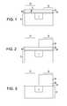
- FIG. 1is a side cross-sectional view depicting a substrate including a first conductivity type region, i.e., n-type device region, and a second conductivity type region, i.e., p-type device region, and a gate stack including a gate dielectric atop the substrate and a first metal gate conductor atop the gate dielectric.
- FIG. 2is a side cross-sectional view depicting forming an etch mask atop the second conductivity type region, wherein the first conductivity type region is exposed.
- FIG. 3is a side cross-sectional view depicting removing a portion of the first metal gate conductor that is present in the first conductivity type region to expose the gate dielectric present in the first conductivity type region, wherein a remaining portion of the metal gate conductor is present in the second conductivity type region.
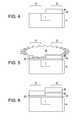
- FIG. 4is a side cross-sectional view depicting removing the etch mask, in accordance with one embodiment of the present invention.
- FIG. 5is a side cross-sectional view depicting applying a nitrogen based plasma to the gate dielectric that is present in the first conductivity type region and the first metal gate conductor that is present in the second conductivity type region.
- FIG. 6is a side cross-sectional view depicting forming a second metal gate conductor atop at least the gate dielectric that is present in the first conductivity type region.
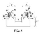
- FIG. 7is a side cross-sectional view depicting one embodiment of forming semiconducting devices from the structure depicted in FIG. 6 .
- the present inventionwhich in one embodiment provides a method for forming gate structures to semiconductor devices, e.g., field effect transistors (FET), having a metal gate conductor/high-k dielectric stack with a threshold voltage tuned to the conductivity type of the semiconductor device, will now be described in greater detail by referring to the following discussion and drawings that accompany the present application. It is noted that the drawings of the present application are provided for illustrative purposes only and, as such, the drawings are not drawn to scale.
- FETfield effect transistors
- semiconductor devicerefers to an intrinsic semiconductor material that has been doped, that is, into which a doping agent has been introduced, giving it different electrical properties than the intrinsic semiconductor.
- Dopingmeans adding dopant atoms to an intrinsic semiconductor, which changes the electron and hole carrier concentrations of the intrinsic semiconductor at thermal equilibrium.
- Dominant carrier concentrations in an extrinsic semiconductorclassify it as either an n-type or p-type semiconductor.
- conductivity typeand “conductivity region” denote a p-type or n-type doped semiconductor.
- P-typerefers to the addition of impurities to an intrinsic semiconductor that creates deficiencies of valence electrons, such as the addition of boron, aluminum, or gallium to a type IV semiconductor, such as silicon.
- N-typerefers to the addition of impurities to an intrinsic semiconductor that contribute free elections, such as the addition of antimony, arsenic, or phosphorous to a type IV semiconductor, such as silicon.
- a “field effect transistor (FET)”is a transistor in which output current, i.e., source-drain current, is controlled by the voltage applied to the gate.
- a field effect transistorhas three terminals, i.e., a gate, a source and a drain.
- drainmeans a doped region semiconductor substrates located at the end of the channel in field effect transistors (FET); in which carriers are flowing out of the transistor through the drain.
- FETfield effect transistors
- sourceis a doped region from which majority carriers are flowing into the channel.
- channelis the region between the source and drain of a metal oxide semiconductor transistor that becomes conductive when the transistor is turned on.
- a “gate structure”means a structure used to control output current (i.e., flow of carriers in the channel) of a semiconducting device, such as a field effect transistor (FET).
- FETfield effect transistor
- gate conductordenotes a material having a bulk resistivity ranging from 10 ⁇ 4 ⁇ -cm to 10 ⁇ 6 ⁇ -cm, which is positioned atop a gate dielectric.
- a “metal”is an electrically conductive material, wherein in metals atoms are held together by the force of metallic bond, and the energy band structure of metal's conduction and valence bands overlap, and hence, there is no energy gap.
- nitridedin reference to nitriding a metal, such as a metal gate conductor, or nitriding a dielectric, such as a gate dielectric, mean that nitrogen is introduced into the material, i.e., dielectric or metal, from an external source.
- a “pFET”refers to a field effect transistor having source/drain regions created by the addition of impurities, such as boron, aluminum or gallium to an intrinsic Si substrate, to create deficiencies of valence electrons to an intrinsic semiconductor.
- an “nFET”refers to a field effect transistor having source/drain regions created by created the addition of impurities that contribute free electrons to an intrinsic semiconductor, such as antimony, arsenic or phosphorous to an intrinsic silicon substrate.
- a “gate dielectric”is a layer of dielectric between the semiconductor device substrate and the gate conductor.
- dielectricdenotes a non-metallic material having insulating properties.
- insulatingdenotes a room temperature conductivity of less than about 10 ⁇ 10 ( ⁇ -m) ⁇ 1 .
- high-kdenotes a dielectric material featuring a dielectric constant (k) higher than 3.9.
- nitrogen based plasmameans a plasma process including a mixture of N 2 and H 2 with no intentional introduction of oxygen or fluorine or any other species.
- Pulsmaas used herein is a collection of charged particles, i.e., particles stripped of at least on electron. Because the particles in the plasma are electrically charged (generally by being stripped of electrons), it is frequently described as an “ionized gas.”
- references in the specification to “one embodiment”, “an embodiment”, “an example embodiment”, etc.,indicate that the embodiment described may include a particular feature, structure, or characteristic, but every embodiment may not necessarily include the particular feature, structure, or characteristic. Moreover, such phrases are not necessarily referring to the same embodiment. Further, when a particular feature, structure, or characteristic is described in connection with an embodiment, it is submitted that it is within the knowledge of one skilled in the art to affect such feature, structure, or characteristic in connection with other embodiments whether or not explicitly described.
- the present inventionprovides a method in which a substrate 5 is exposed to an ambience containing a N 2 or a N 2 /H 2 (hereinafter N/H) plasma.
- N/Ha N 2 or a N 2 /H 2
- the application of the N or N/H plasmanitrides a gate dielectric that is present in portions of the substrate in which n-type conductivity semiconductor devices are subsequently formed, and nitrides a metal gate conductor that is present in portions of the substrate in which the p-type conductivity semiconductor devices are subsequently formed.
- a nitrided gate dielectricmay improve device performance in n-type semiconductor devices by mitigating the device dimension dependent regrowth and causing a desirable threshold voltage (Vt) shift in the direction of a higher work function towards the pFET band-edge (4.9 eV to 5.2 eV).
- a nitrided metal gate conductormay improve device performance in p-type semiconductor devices by increasing the work function that is increasing with the N dose, which results in a desirable threshold voltage (Vt) that is consistent with the desired pFET workfunctions of 4.9 eV to 5.2 eV for p-type semiconductor devices.
- FIGS. 1-7depicts one embodiment of a process for forming gate structures to a complementary metal oxide semiconductor (CMOS device).
- the methodincludes providing a substrate 5 including a first conductivity type region 10 , e.g. n-type device region, and a second conductivity region 15 , e.g., p-type device region, wherein a gate stack 55 including a gate dielectric 20 is present atop the first conductivity type region 10 and the second conductivity type region 15 and a first metal gate conductor 60 that is present overlying the gate dielectric 20 .
- a portion of the first metal gate conductor 60 that is present in the first conductivity type region 10is removed to expose the underlying gate dielectric 20 .
- removing the portion of the first metal gate conductor 60includes forming an etch mask 24 over the second conductivity type region 15 , wherein the first conductivity type region 10 is exposed, and removing, e.g., etching, a portion of the first metal gate conductor 60 over the first conductivity type region 15 to expose a portion of the gate dielectric 20 that is present in the first conductivity type region 15 .
- the etch mask 24is removed and a nitrogen based plasma 50 is then applied to nitride the exposed portion of the gate dielectric 20 in the first conductivity device region 10 and the remaining portion of the first metal gate conductor 60 that is present in the second conductivity type region 15 .
- the first conductivity type region 10provides the site for a subsequently formed nFET device and the second conductivity type region 15 provides the site for a subsequently formed pFET device. In another embodiment, the first conductivity type region 10 provides the site for a subsequently formed pFET device and the second conductivity type region 15 provides the site for a subsequently formed nFET device.
- the substrate 5 employed in the present inventionmay be any semiconducting material including, but not limited to: Si, Ge, SiGe, SiC, SiGeC, Ga, GaAs, InAs, InP and all other III/V or II/VI compound semiconductors.
- the substrate 5may also include an organic semiconductor or a layered semiconductor such as Si/SiGe, a silicon-on-insulator (SOI) or a SiGe-on-insulator (SGOI).
- the substrate 5is composed of a Si-containing semiconductor material, i.e., a semiconductor material that includes silicon.
- the substrate 5may be doped, undoped or contain doped and undoped regions therein.
- the substrate 5may also include a first doped (n- or p-) region, and a second doped (n- or p-) region.
- n- or p-first doped
- n- or p-second doped
- the first doped region and the second doped regionmay be the same, or they may have different conductivities and/or doping concentrations. These doped regions are known as “wells”.
- At least one isolation region 1is typically present within the substrate 5 .
- the at least one isolation region 1may be a trench isolation region or a field oxide isolation region.
- the trench isolation regionis formed utilizing a trench isolation process well known to those skilled in the art. For example, lithography, etching and filling of the trench with a trench dielectric may be used in forming the trench isolation region.
- a linermay be formed in the trench prior to trench fill, a densification step may be performed after the trench fill and a planarization process may follow the trench fill as well.
- the field oxidemay be formed utilizing a local oxidation of silicon process.
- the at least one isolation region 1provides isolation between neighboring first conductivity type regions 10 and second conductivity type regions 15 , typically required when the neighboring gates have opposite conductivities.
- a semiconducting regionis defined by the portion of the substrate 5 that is positioned between two isolation regions 1 .
- a gate stack 55is formed atop the first conductivity type region 10 and the second conductivity type region 15 of the substrate 5 .
- the gate stack 55includes at least a gate dielectric 20 and a gate conductor 60 that is located atop gate dielectric 20 .
- the gate dielectric 20 of the gate stack 55may be formed on a surface of the substrate 5 .
- the gate dielectric 20is formed atop the first conductivity type region 10 and the second conductivity type region 15 of the substrate 5 .
- the gate dielectric 20is composed of a high-k gate dielectric material.
- the high-k dielectric materialis formed by a thermal growth process, such as, for example, oxidation, nitridation or oxynitridation.
- the high-k dielectric materialis formed by a deposition process such as, for example, chemical vapor deposition (CVD), plasma-assisted CVD, metal organic chemical vapor deposition (MOCVD), atomic layer deposition (ALD), evaporation, reactive sputtering, chemical solution deposition and other like deposition processes.
- the high-k dielectric materialmay also be formed utilizing any combination of the above processes.
- the high-k dielectric material used as the gate dielectric 20includes an insulating material having a dielectric constant of greater than 4.0.
- the high-k dielectric materialhas a dielectric constant greater than 7.0.
- the high-k dielectric material employed for the gate dielectric 20 in the present inventionincludes, but not limited to: an oxide, nitride, oxynitride and/or silicate including metal silicates and nitrided metal silicates.
- the high-k dielectric materialis composed of HfO 2 , hafnium silicate and hafnium silicon oxynitride.
- the gate dielectric 20includes a high-k dielectric material composed of an oxide, such as, for example, ZrO 2 , Al 2 O 3 , TiO 2 , La 2 O 3 , SrTiO 3 , LaAlO 3 , Y 2 O 3 and mixtures thereof.
- a high-k dielectric materialcomposed of an oxide, such as, for example, ZrO 2 , Al 2 O 3 , TiO 2 , La 2 O 3 , SrTiO 3 , LaAlO 3 , Y 2 O 3 and mixtures thereof.
- the physical thickness of the high-k dielectric materialmay vary, but in one embodiment of the present invention, the high-k dielectric material has a thickness ranging from 0.5 nm to 10 nm, with a thickness from 0.5 nm to 3 nm being more typical. It may be deposited above a thin (on the order of 0.1 nm to 1.5 nm) layer of silicon oxide or silicon oxynitride that is first deposited on the substrate 5 . In some instances, an additional dielectric layer can be located between the gate dielectric 20 and the substrate 5 , such as a nitride layer.
- a first metal gate conductor 60is then formed overlying the gate dielectric 20 .
- the first metal gate conductor 60is formed atop the gate dielectric 20 utilizing a deposition process, such as CVD, plasma-assisted CVD, plating, and/or sputtering, followed by planarization.
- the first metal gate conductor 60may include any conductive metal including, but not limited to: W, Ni, Ti, Mo, Ta, Cu, Pt, Ag, Au, Ru, Ir, Rh, and Re, and alloys that include at least one of the aforementioned conductive elemental metals, such as TiN, TaN, MoN etc.
- the first metal gate conductor 60may have a thickness T 1 ranging from 5 nm to 50 nm. More typically, the thickness T 1 of the first metal gate conductor 60 ranges from 7.5 nm to 20 nm.
- an etch mask 24is formed atop the gate dielectric 20 on the second conductivity type region 15 .
- formation of the etch mask 24begins with depositing a photoresist layer atop the first conductivity type region 10 and the second conductivity type region 15 .
- the photoresist layercan be either positive-acting or negative-acting.
- those coating layer portions that are exposed to an activating radiationpolymerize or cross-link in a reaction between a photoactive compound and polymerizable agents of the photoresist composition. Consequently, the exposed coating portions are rendered less soluble in a developer solution than unexposed portions.
- exposed portionsare rendered more soluble in a developer solution while areas not exposed remain comparatively less developer soluble.
- photoresist compositionsinclude at least a resin binder component and a photoactive agent.
- a resin binder componentand a photoactive agent.
- a wide variety of polymeric or resin bindersmay be used in photoresists. Such polymeric binders may include, as polymerized components, one or more acid functional monomers such as acrylic acid or methacrylic acid.
- the photoresist layeris composed of DQN photoresist.
- DQN photoresistis a two component photoresist that includes diazoquinone (DQ)-photosensitive component) and novolac (N-resin).
- DQdiazoquinone
- N-resinnovolac
- the diazoquinoneis the photosensitive component and the novolac is not sensitive enough for ⁇ 300 nm exposure wavelength; common with g-line (436 nm) and i-line (365 nm) exposure tools.
- the photoresistmay be either liquid or dry film. Liquid photoresists are dispensed on a substrate and then cured. Dry film photoresists are typically laminated to a substrate.
- the photoresist layeris deposited using spin-on techniques.
- the photoresist layeris patterned using photolithography and developed to provide the etch mask 24 . More specifically, in one embodiment, a pattern is produced by exposing the photoresist layer to a pattern of radiation, and then developing the pattern into the photoresist utilizing conventional resist developer, such as a chemical solvent. In a positive resist development, the developer leaves a hole in the resist layer that corresponds to the opaque pattern of a reticle (mask) of the photolithography tool. In negative resist development, the developer leaves a pattern in the resist opposite to that on the reticle (mask). Development of the pattern is conducted using conventional development techniques including, but not limited to: continuous spray development and puddle development. In another embodiment, the etch mask 24 may be a hard mask composed of an oxide, nitride or oxynitride material.
- one of the first conductivity type region 10 and the second conductivity type region 15is exposed, wherein a remaining portion of the photoresist layer remains overlying the other of the first conductivity type region 10 or the second conductivity type region 15 . It is noted that although FIG.
- the method of the present inventionis equally applicable to where the remaining portion of the photoresist layer, i.e., the etch mask 24 , is positioned overlying the first conductivity type region 10 , i.e., n-type device region.
- FIG. 3depicts etching the exposed portion of the first metal gate conductor 60 stopping on the gate dielectric 20 in the first conductivity type region 10 , i.e., n-type device region, in which the etch mask 24 protects the portion of the first metal gate conductor 60 that is present in the second conductivity type region 15 , i.e, p-type device region.
- the etch processis provide by an anisotropic etch, such as reactive ion etch.
- the etch processremoves the first metal gate conductor 60 selective to the gate dielectric 20 .
- the etch process that removes the first metal gate conductor 60includes an etch chemistry composed of Cl 2 and Ar.
- the etch mask 24is removed, as depicted in FIG. 4 .
- the etch mask 24may be removed using oxygen ashing.
- a nitrogen based plasma 50is then applied to the first conductivity type region 10 and the second conductivity type region 15 of the substrate 5 , wherein the nitrogen based plasma 50 produces a nitrogen containing layer 26 on and/or within the exposed portion of the gate dielectric 20 in the first conductivity type region 10 , i.e., n-type device region, and produces a nitrogen containing layer 26 on and/or within the remaining portion of the first metal gate conductor 60 in the second conductivity type region 15 , i.e., p-type device region.
- the nitrogen based plasma 50nitrides the gate dielectric 20 that is present in the first conductivity type region 10 and nitrides the first metal gate conductor 60 that is present in the second conductivity type region 15 , wherein the nitrogen content in the gate dielectric 20 ranges from 0% to 50%, and the nitrogen content of the first metal gate conductor 60 ranges from 0% to 60%. In some instances, the nitrogen content of the gate dielectric 20 may be greater than 50%, and in some instances the nitrogen content of the first metal gate conductor 60 may be greater than 60%.
- the nitrogen containing layer 26 that is present in the first conductivity type region 10is a portion of the exposed portion of the gate dielectric 20 that has a thickness ranging from 1 nm to 10 nm, as measured from the top surface of the gate dielectric 20 , and has a nitrogen concentration ranging from 0% to 50%, typically being greater than 1%.
- the nitrogen concentration in the aforementioned portion of the gate dielectric 20ranges from 10% to 50%, typically ranging from 25% to 50%.
- the nitrogen containing layer 26 that is present in the second conductivity type region 15is a remaining portion of the first metal gate conductor 60 that has a thickness ranging from 1 nm to 20 nm, as measured from the top surface of the first metal gate conductor 60 , and has a nitrogen concentration ranging from 0% to 60%, typically being greater than 1%.
- the nitrogen concentration in the aforementioned portion of the first metal gate conductor 60ranges from 10% to 60%, typically ranging from 25% to 60%.
- a nitrided gate dielectric 20 , 26may improve device performance in semiconductor devices by mitigating the device dimension regrowth effect and causing a desirable threshold voltage (Vt) shift that is dependent on the N dose added and is controlled to the shifts needed.
- a nitrided metal gate conductor 26 , 60may improve device performance, in p-type semiconductor devices by increasing the effective work function to a value ranging from 4.9 eV to 5.2 eV, which results in a desirable threshold voltage (Vt) for p-type semiconductor devices.
- the effective work function of the n-type semiconductor devicesranges from 4.1 eV to 4.3 eV.
- a n-type semiconductor device incorporating the gate dielectric 20 having the nitride containing layer 26 present thereon/thereinmay have a threshold voltage ranging from about 0.0 mV to about 300 mV.
- a p-type semiconductor device incorporating the first metal gate conductor 60 having the nitride containing layer 26 present thereon/thereinmay have a threshold voltage ranging from about 0.0 mV to about 300 mV.
- the nitrogen based plasma 50is composed of N 2 /H 2 .
- the nitrogen based plasmamay further include radicals composed of O 2 and Si.
- the nitrogen based plasma 50is composed of 1% to 10% of H 2 in N 2 /H 2 and is substantially free of O 2 .
- the O 2 content of the nitrogen based plasma 50is less than 0.01%.
- the O 2 content of the nitrogen based plasma 50is less than 0.5%.
- the nitrogen based plasma 50is completely devoid of O 2 .
- the fluoride content of the nitrogen based plasma 50is 0.5% or less. In another example, the nitrogen based plasma 50 is completely devoid, i.e., 0.0%, of fluoride.
- the flow rate of the nitrogen based plasma 50ranges from 2,000 sccm to 11,000 sccm. In another embodiment, the flow rate of the nitrogen based plasma 50 ranges from 8,000 sccm to 10,000 sccm.
- the RF power of the nitrogen based plasma 50ranges from 1,000 W to 3,000 W. More typically, the RF power of the nitrogen based plasma 50 ranges from 1,500 W to 2,500 W. Even more typically, the RF power of the nitrogen based plasma ranges 50 from 500 W to 5000 W.
- the temperature during the application of the nitrogen based plasma 50ranges from about room temperature to 300° C. In another embodiment, the temperature during the application of the nitrogen based plasma 50 ranges from 25° C. to 350° C. In a further embodiment, the temperature during the application of the nitrogen based plasma 50 ranges from 100° C. to 300° C.
- a second metal gate conductor 65may be deposited atop the nitride containing layer 26 in the first conductivity type region 10 and the second conductivity type region 15 .
- the second metal gate conductor 60may be deposited by physical vapor deposition (PVD), e.g., sputtering or plating.
- PVDphysical vapor deposition
- the second metal gate conductor 65is composed of TaN, W, WN, Ti, TiN or combinations thereof.
- the second metal gate conductor 65has a thickness ranging from 1 nm to 50 nm.
- the first conductivity type region 10 and the second conductivity type region 15may be processed to provide semiconducting devices.
- the nitrided gate dielectric 20 , 26(also referred to as the portion of the gate dielectric 20 that includes a nitrogen containing layer 26 and is present in the first conductivity type region 10 ) may provide the gate dielectric of a gate structure to an n-type field effect transistor (FET).
- FETfield effect transistors
- FETsfield effect transistors
- An nFETmay be formed including a first metal gate conductor 60 composed of titanium nitride (TiN) and a nitrided gate dielectric 20 , 26 composed of a high-k dielectric material, such as hafnium oxide (HfO 2 ), wherein a layer of aluminum oxide (Al 2 O 3 ) may be present at the interface of the first metal gate conductor 60 and the nitrided gate conductor 26 , 60 .
- the nFETincludes a metal gate conductor composed of tungsten nitride (WN) and a high-k dielectric material 20 composed of HfO 2 .
- a pFETmay be formed including a nitrided first metal gate conductor 26 , 60 (also referred to as the remaining portion of the first metal gate conductor 60 that includes a nitrogen containing layer 26 and is present in the second conductivity type region 15 ) composed of titanium nitride (TiN) and a gate dielectric 20 composed of hafnium oxide (HfO 2 ), wherein a layer of tantalum oxide (TaO) may be present at the interface of the nitrided first metal gate conductor 26 , 60 and the gate dielectric 20 .
- a nitrided first metal gate conductor 26 , 60also referred to as the remaining portion of the first metal gate conductor 60 that includes a nitrogen containing layer 26 and is present in the second conductivity type region 15
- TiNtitanium nitride
- HfO 2hafnium oxide
- TaOtantalum oxide
- the layered stack including the second metal gate conductor 65 , the nitrogen containing layer 26 , the first metal gate conductor 60 , and the high-k dielectric material 20is patterned and etched to provide a first gate structures 70 in the first conductivity region 10 and a second gate structure 80 in the second conductivity region 15 of the substrate 5 .
- the first gate structure 70includes the nitrided gate dielectric 20 , 26 , and the second metal gate conductor 65
- the second gate structure 80includes the high-k dielectric material 20 , the nitrided gate conductor 26 , 60 , and the second metal gate conductor 65 .
- forming the gate stacks 70 , 80may include depositing a layer of photoresist (not shown) atop the entire structure depicted in FIG. 6 .
- the photoresist layeris then selectively patterned and developed to provide an photoresist mask (etch mask) (not shown) protecting the portion of layered stack of the second metal gate conductor 65 /first metal gate conductor 60 /high-k dielectric material 20 corresponding to the subsequently formed gate stacks 70 , 80 .
- the exposed regions of the layered stack of the metal gate conductor 60 /high-k dielectric material 20are then etched, while the regions underlying the photoresist mask are protected to provide the gate stacks 70 , 80 corresponding to FET devices.
- the photoresist maskis removed by a stripping process, such as oxygen ashing.
- extension source and drain regions 85may then be formed in the first conductivity region 10 and the second conductivity region 15 of the substrate 5 .
- Source and drain offset spacers 90may then formed abutting the first gate structure 70 and the second gate structure 80 , and deep source and drain regions 95 are formed in the first conductivity region 10 and the second conductivity region 15 of the substrate 5 , as depicted in FIG. 7 .
- the aforementioned methodprovides the semiconductor device depicted in FIG. 7 .
- the semiconductor deviceincludes a substrate 5 having a p-type device region (first conductivity region 10 ) and an n-type device region (second conductivity region 15 ), in which at least one nFET present in the n-type device region and at least one pFET is present in the p-type device region.
- each of the at least one nFETincludes a gate structure (gate stack 70 ) including a Hf-containing gate dielectric (high-k gate dielectric 20 ) present on the substrate 5 having a nitrided upper surface (nitrogen containing layer 26 ), and a gate conductor (second metal gate conductor 65 ) directly on the nitrided upper surface of the Hf-containing gate dielectric.
- gate stack 70gate structure including a Hf-containing gate dielectric (high-k gate dielectric 20 ) present on the substrate 5 having a nitrided upper surface (nitrogen containing layer 26 ), and a gate conductor (second metal gate conductor 65 ) directly on the nitrided upper surface of the Hf-containing gate dielectric.
- each of the at least one pFETincludes a gate structure (gate stack 80 ) including a Hf-containing gate dielectric (high-k gate dielectric 20 ) present on the substrate 5 having an upper surface substantially free of nitride, and a gate conductor (first metal gate conductor 60 ) present directly on the Hf-containing gate dielectric having the upper surface substantially free of nitride, wherein an upper surface of the gate conductor in the gate structure of the at least one pFET is a nitrided upper surface (nitrogen containing layer 26 ).
- gate structuregate stack 80
- gate stack 80including a Hf-containing gate dielectric (high-k gate dielectric 20 ) present on the substrate 5 having an upper surface substantially free of nitride, and a gate conductor (first metal gate conductor 60 ) present directly on the Hf-containing gate dielectric having the upper surface substantially free of nitride, wherein an upper surface of the gate conductor in the gate structure of the at least one pFET is
- the substantially free of nitridemeans less than 10.0% nitride, typically less than 5.0% nitride, more typically less than 1.0% nitride, and in some embodiments 0.0% nitride.
- the gate structure to the at least one pFETfurther includes another gate conductor present on the upper surface of the gate conductor that has the nitrided upper surface (second metal gate conductor 65 ).
Landscapes
- Engineering & Computer Science (AREA)
- Manufacturing & Machinery (AREA)
- Power Engineering (AREA)
- General Chemical & Material Sciences (AREA)
- Physics & Mathematics (AREA)
- Chemical Kinetics & Catalysis (AREA)
- Condensed Matter Physics & Semiconductors (AREA)
- Crystallography & Structural Chemistry (AREA)
- Computer Hardware Design (AREA)
- General Physics & Mathematics (AREA)
- Microelectronics & Electronic Packaging (AREA)
- Chemical & Material Sciences (AREA)
- Electrodes Of Semiconductors (AREA)
- Insulated Gate Type Field-Effect Transistor (AREA)
- Metal-Oxide And Bipolar Metal-Oxide Semiconductor Integrated Circuits (AREA)
- Thin Film Transistor (AREA)
Abstract
Description
Claims (20)
Priority Applications (1)
| Application Number | Priority Date | Filing Date | Title |
|---|---|---|---|
| US13/080,962US8436427B2 (en) | 2009-04-14 | 2011-04-06 | Dual metal and dual dielectric integration for metal high-K FETs |
Applications Claiming Priority (2)
| Application Number | Priority Date | Filing Date | Title |
|---|---|---|---|
| US12/423,236US7943457B2 (en) | 2009-04-14 | 2009-04-14 | Dual metal and dual dielectric integration for metal high-k FETs |
| US13/080,962US8436427B2 (en) | 2009-04-14 | 2011-04-06 | Dual metal and dual dielectric integration for metal high-K FETs |
Related Parent Applications (1)
| Application Number | Title | Priority Date | Filing Date |
|---|---|---|---|
| US12/423,236DivisionUS7943457B2 (en) | 2009-04-14 | 2009-04-14 | Dual metal and dual dielectric integration for metal high-k FETs |
Publications (2)
| Publication Number | Publication Date |
|---|---|
| US20110180880A1 US20110180880A1 (en) | 2011-07-28 |
| US8436427B2true US8436427B2 (en) | 2013-05-07 |
Family
ID=42933697
Family Applications (2)
| Application Number | Title | Priority Date | Filing Date |
|---|---|---|---|
| US12/423,236ActiveUS7943457B2 (en) | 2009-04-14 | 2009-04-14 | Dual metal and dual dielectric integration for metal high-k FETs |
| US13/080,962ActiveUS8436427B2 (en) | 2009-04-14 | 2011-04-06 | Dual metal and dual dielectric integration for metal high-K FETs |
Family Applications Before (1)
| Application Number | Title | Priority Date | Filing Date |
|---|---|---|---|
| US12/423,236ActiveUS7943457B2 (en) | 2009-04-14 | 2009-04-14 | Dual metal and dual dielectric integration for metal high-k FETs |
Country Status (7)
| Country | Link |
|---|---|
| US (2) | US7943457B2 (en) |
| EP (1) | EP2419925B1 (en) |
| JP (1) | JP5579828B2 (en) |
| CN (1) | CN102341894A (en) |
| BR (1) | BRPI1006585A2 (en) |
| TW (1) | TWI476822B (en) |
| WO (1) | WO2010120842A1 (en) |
Cited By (2)
| Publication number | Priority date | Publication date | Assignee | Title |
|---|---|---|---|---|
| US9786761B2 (en) | 2015-04-21 | 2017-10-10 | Samsung Electronics Co., Ltd. | Integrated circuit device having an interfacial layer and method of manufacturing the same |
| US11239083B2 (en) | 2019-03-11 | 2022-02-01 | Taiwan Semiconductor Manufacturing Company, Ltd. | Tuning threshold voltage through meta stable plasma treatment |
Families Citing this family (67)
| Publication number | Priority date | Publication date | Assignee | Title |
|---|---|---|---|---|
| US8106455B2 (en)* | 2009-04-30 | 2012-01-31 | International Business Machines Corporation | Threshold voltage adjustment through gate dielectric stack modification |
| US8421162B2 (en) | 2009-09-30 | 2013-04-16 | Suvolta, Inc. | Advanced transistors with punch through suppression |
| US8273617B2 (en) | 2009-09-30 | 2012-09-25 | Suvolta, Inc. | Electronic devices and systems, and methods for making and using the same |
| US7943458B2 (en)* | 2009-10-06 | 2011-05-17 | International Business Machines Corporation | Methods for obtaining gate stacks with tunable threshold voltage and scaling |
| US8530286B2 (en) | 2010-04-12 | 2013-09-10 | Suvolta, Inc. | Low power semiconductor transistor structure and method of fabrication thereof |
| US8354313B2 (en)* | 2010-04-30 | 2013-01-15 | International Business Machines Corporation | Method to optimize work function in complementary metal oxide semiconductor (CMOS) structures |
| US8569128B2 (en) | 2010-06-21 | 2013-10-29 | Suvolta, Inc. | Semiconductor structure and method of fabrication thereof with mixed metal types |
| US8759872B2 (en) | 2010-06-22 | 2014-06-24 | Suvolta, Inc. | Transistor with threshold voltage set notch and method of fabrication thereof |
| US8377783B2 (en) | 2010-09-30 | 2013-02-19 | Suvolta, Inc. | Method for reducing punch-through in a transistor device |
| US8404551B2 (en) | 2010-12-03 | 2013-03-26 | Suvolta, Inc. | Source/drain extension control for advanced transistors |
| US8461875B1 (en) | 2011-02-18 | 2013-06-11 | Suvolta, Inc. | Digital circuits having improved transistors, and methods therefor |
| US8525271B2 (en) | 2011-03-03 | 2013-09-03 | Suvolta, Inc. | Semiconductor structure with improved channel stack and method for fabrication thereof |
| TWI566300B (en)* | 2011-03-23 | 2017-01-11 | 斯克林集團公司 | Heat treatment method and heat treatment apparatus for heating substrate by irradiating substrate with light |
| US8400219B2 (en) | 2011-03-24 | 2013-03-19 | Suvolta, Inc. | Analog circuits having improved transistors, and methods therefor |
| US8748270B1 (en) | 2011-03-30 | 2014-06-10 | Suvolta, Inc. | Process for manufacturing an improved analog transistor |
| US8999861B1 (en) | 2011-05-11 | 2015-04-07 | Suvolta, Inc. | Semiconductor structure with substitutional boron and method for fabrication thereof |
| US8796048B1 (en) | 2011-05-11 | 2014-08-05 | Suvolta, Inc. | Monitoring and measurement of thin film layers |
| US8811068B1 (en) | 2011-05-13 | 2014-08-19 | Suvolta, Inc. | Integrated circuit devices and methods |
| US8569156B1 (en) | 2011-05-16 | 2013-10-29 | Suvolta, Inc. | Reducing or eliminating pre-amorphization in transistor manufacture |
| US8735987B1 (en) | 2011-06-06 | 2014-05-27 | Suvolta, Inc. | CMOS gate stack structures and processes |
| US8995204B2 (en) | 2011-06-23 | 2015-03-31 | Suvolta, Inc. | Circuit devices and methods having adjustable transistor body bias |
| US8629016B1 (en) | 2011-07-26 | 2014-01-14 | Suvolta, Inc. | Multiple transistor types formed in a common epitaxial layer by differential out-diffusion from a doped underlayer |
| KR101891373B1 (en) | 2011-08-05 | 2018-08-24 | 엠아이이 후지쯔 세미컨덕터 리미티드 | Semiconductor devices having fin structures and fabrication methods thereof |
| US8748986B1 (en) | 2011-08-05 | 2014-06-10 | Suvolta, Inc. | Electronic device with controlled threshold voltage |
| US8645878B1 (en) | 2011-08-23 | 2014-02-04 | Suvolta, Inc. | Porting a circuit design from a first semiconductor process to a second semiconductor process |
| US8614128B1 (en) | 2011-08-23 | 2013-12-24 | Suvolta, Inc. | CMOS structures and processes based on selective thinning |
| US8713511B1 (en) | 2011-09-16 | 2014-04-29 | Suvolta, Inc. | Tools and methods for yield-aware semiconductor manufacturing process target generation |
| US9236466B1 (en) | 2011-10-07 | 2016-01-12 | Mie Fujitsu Semiconductor Limited | Analog circuits having improved insulated gate transistors, and methods therefor |
| US9595443B2 (en) | 2011-10-20 | 2017-03-14 | Taiwan Semiconductor Manufacturing Company, Ltd. | Metal gate structure of a semiconductor device |
| US8895327B1 (en) | 2011-12-09 | 2014-11-25 | Suvolta, Inc. | Tipless transistors, short-tip transistors, and methods and circuits therefor |
| US8819603B1 (en) | 2011-12-15 | 2014-08-26 | Suvolta, Inc. | Memory circuits and methods of making and designing the same |
| US8883600B1 (en) | 2011-12-22 | 2014-11-11 | Suvolta, Inc. | Transistor having reduced junction leakage and methods of forming thereof |
| US8599623B1 (en) | 2011-12-23 | 2013-12-03 | Suvolta, Inc. | Circuits and methods for measuring circuit elements in an integrated circuit device |
| US8970289B1 (en) | 2012-01-23 | 2015-03-03 | Suvolta, Inc. | Circuits and devices for generating bi-directional body bias voltages, and methods therefor |
| US8877619B1 (en) | 2012-01-23 | 2014-11-04 | Suvolta, Inc. | Process for manufacture of integrated circuits with different channel doping transistor architectures and devices therefrom |
| US9093550B1 (en) | 2012-01-31 | 2015-07-28 | Mie Fujitsu Semiconductor Limited | Integrated circuits having a plurality of high-K metal gate FETs with various combinations of channel foundation structure and gate stack structure and methods of making same |
| US9406567B1 (en) | 2012-02-28 | 2016-08-02 | Mie Fujitsu Semiconductor Limited | Method for fabricating multiple transistor devices on a substrate with varying threshold voltages |
| US8863064B1 (en) | 2012-03-23 | 2014-10-14 | Suvolta, Inc. | SRAM cell layout structure and devices therefrom |
| US9299698B2 (en) | 2012-06-27 | 2016-03-29 | Mie Fujitsu Semiconductor Limited | Semiconductor structure with multiple transistors having various threshold voltages |
| US8941177B2 (en) | 2012-06-27 | 2015-01-27 | International Business Machines Corporation | Semiconductor devices having different gate oxide thicknesses |
| KR20140016694A (en)* | 2012-07-31 | 2014-02-10 | 삼성전자주식회사 | Semiconductor devices and methods of manufacturing the same |
| US8637955B1 (en) | 2012-08-31 | 2014-01-28 | Suvolta, Inc. | Semiconductor structure with reduced junction leakage and method of fabrication thereof |
| US9112057B1 (en) | 2012-09-18 | 2015-08-18 | Mie Fujitsu Semiconductor Limited | Semiconductor devices with dopant migration suppression and method of fabrication thereof |
| US9041126B2 (en) | 2012-09-21 | 2015-05-26 | Mie Fujitsu Semiconductor Limited | Deeply depleted MOS transistors having a screening layer and methods thereof |
| US8829616B2 (en) | 2012-10-25 | 2014-09-09 | International Business Machines Corporation | Method and structure for body contacted FET with reduced body resistance and source to drain contact leakage |
| US9431068B2 (en) | 2012-10-31 | 2016-08-30 | Mie Fujitsu Semiconductor Limited | Dynamic random access memory (DRAM) with low variation transistor peripheral circuits |
| US8816754B1 (en) | 2012-11-02 | 2014-08-26 | Suvolta, Inc. | Body bias circuits and methods |
| US9093997B1 (en) | 2012-11-15 | 2015-07-28 | Mie Fujitsu Semiconductor Limited | Slew based process and bias monitors and related methods |
| US9070477B1 (en) | 2012-12-12 | 2015-06-30 | Mie Fujitsu Semiconductor Limited | Bit interleaved low voltage static random access memory (SRAM) and related methods |
| US9112484B1 (en) | 2012-12-20 | 2015-08-18 | Mie Fujitsu Semiconductor Limited | Integrated circuit process and bias monitors and related methods |
| US9268885B1 (en) | 2013-02-28 | 2016-02-23 | Mie Fujitsu Semiconductor Limited | Integrated circuit device methods and models with predicted device metric variations |
| US8994415B1 (en) | 2013-03-01 | 2015-03-31 | Suvolta, Inc. | Multiple VDD clock buffer |
| US8988153B1 (en) | 2013-03-09 | 2015-03-24 | Suvolta, Inc. | Ring oscillator with NMOS or PMOS variation insensitivity |
| US9299801B1 (en) | 2013-03-14 | 2016-03-29 | Mie Fujitsu Semiconductor Limited | Method for fabricating a transistor device with a tuned dopant profile |
| US9112495B1 (en) | 2013-03-15 | 2015-08-18 | Mie Fujitsu Semiconductor Limited | Integrated circuit device body bias circuits and methods |
| US9449967B1 (en) | 2013-03-15 | 2016-09-20 | Fujitsu Semiconductor Limited | Transistor array structure |
| US9219078B2 (en) | 2013-04-18 | 2015-12-22 | International Business Machines Corporation | Simplified multi-threshold voltage scheme for fully depleted SOI MOSFETs |
| US9478571B1 (en) | 2013-05-24 | 2016-10-25 | Mie Fujitsu Semiconductor Limited | Buried channel deeply depleted channel transistor |
| US8976575B1 (en) | 2013-08-29 | 2015-03-10 | Suvolta, Inc. | SRAM performance monitor |
| US9093387B1 (en)* | 2014-01-08 | 2015-07-28 | International Business Machines Corporation | Metallic mask patterning process for minimizing collateral etch of an underlayer |
| US9710006B2 (en) | 2014-07-25 | 2017-07-18 | Mie Fujitsu Semiconductor Limited | Power up body bias circuits and methods |
| US9319013B2 (en) | 2014-08-19 | 2016-04-19 | Mie Fujitsu Semiconductor Limited | Operational amplifier input offset correction with transistor threshold voltage adjustment |
| US9837487B2 (en) | 2015-11-30 | 2017-12-05 | Taiwan Semiconductor Manufacturing Co., Ltd. | Structure and formation method of semiconductor device structure with gate stack |
| US9768171B2 (en)* | 2015-12-16 | 2017-09-19 | International Business Machines Corporation | Method to form dual tin layers as pFET work metal stack |
| US9559016B1 (en)* | 2016-01-15 | 2017-01-31 | International Business Machines Corporation | Semiconductor device having a gate stack with tunable work function |
| US10062693B2 (en) | 2016-02-24 | 2018-08-28 | International Business Machines Corporation | Patterned gate dielectrics for III-V-based CMOS circuits |
| US10593600B2 (en) | 2016-02-24 | 2020-03-17 | International Business Machines Corporation | Distinct gate stacks for III-V-based CMOS circuits comprising a channel cap |
Citations (23)
| Publication number | Priority date | Publication date | Assignee | Title |
|---|---|---|---|---|
| US6693004B1 (en) | 2002-02-27 | 2004-02-17 | Advanced Micro Devices, Inc. | Interfacial barrier layer in semiconductor devices with high-K gate dielectric material |
| US20040092073A1 (en) | 2002-11-08 | 2004-05-13 | Cyril Cabral | Deposition of hafnium oxide and/or zirconium oxide and fabrication of passivated electronic structures |
| US6750066B1 (en) | 2002-04-08 | 2004-06-15 | Advanced Micro Devices, Inc. | Precision high-K intergate dielectric layer |
| US6767847B1 (en) | 2002-07-02 | 2004-07-27 | Taiwan Semiconductor Manufacturing Company | Method of forming a silicon nitride-silicon dioxide gate stack |
| US20050035417A1 (en) | 2003-08-13 | 2005-02-17 | Visokay Mark R. | Dual metal-alloy nitride gate electrodes |
| US6893984B2 (en) | 2002-02-20 | 2005-05-17 | Micron Technology Inc. | Evaporated LaA1O3 films for gate dielectrics |
| US6979855B2 (en) | 2001-12-20 | 2005-12-27 | Micron Technology, Inc. | High-quality praseodymium gate dielectrics |
| US7091118B1 (en) | 2004-11-16 | 2006-08-15 | Advanced Micro Devices, Inc. | Replacement metal gate transistor with metal-rich silicon layer and method for making the same |
| US20060237803A1 (en) | 2005-04-21 | 2006-10-26 | International Business Machines Corporation | ULTRA-THIN Hf-DOPED-SILICON OXYNITRIDE FILM FOR HIGH PERFORMANCE CMOS APPLICATIONS AND METHOD OF MANUFACTURE |
| US7135369B2 (en) | 2003-03-31 | 2006-11-14 | Micron Technology, Inc. | Atomic layer deposited ZrAlxOy dielectric layers including Zr4AlO9 |
| US7135421B2 (en) | 2002-06-05 | 2006-11-14 | Micron Technology, Inc. | Atomic layer-deposited hafnium aluminum oxide |
| US20060286802A1 (en) | 2005-05-11 | 2006-12-21 | Hongyu Yu | Low work function metal alloy |
| US7160577B2 (en) | 2002-05-02 | 2007-01-09 | Micron Technology, Inc. | Methods for atomic-layer deposition of aluminum oxides in integrated circuits |
| US7192892B2 (en) | 2003-03-04 | 2007-03-20 | Micron Technology, Inc. | Atomic layer deposited dielectric layers |
| US7205620B2 (en) | 2002-01-17 | 2007-04-17 | Micron Technology, Inc. | Highly reliable amorphous high-k gate dielectric ZrOxNy |
| US20070138563A1 (en) | 2005-12-16 | 2007-06-21 | International Business Machines Corporation | Dual metal gate self-aligned integration |
| US20070152276A1 (en) | 2005-12-30 | 2007-07-05 | International Business Machines Corporation | High performance CMOS circuits, and methods for fabricating the same |
| US20070152273A1 (en) | 2005-12-30 | 2007-07-05 | International Bunisess Machines Corporation | High performance circuit with metal and polygate electrodes |
| US7259434B2 (en) | 2001-08-30 | 2007-08-21 | Micron Technology, Inc. | Highly reliable amorphous high-k gate oxide ZrO2 |
| US20080191292A1 (en) | 2007-02-12 | 2008-08-14 | International Business Machines Corporation | METAL GATES WITH LOW CHARGE TRAPPING AND ENHANCED DIELECTRIC RELIABILITY CHARACTERISTICS FOR HIGH-k GATE DIELECTRIC STACKS |
| US20080203485A1 (en) | 2007-02-28 | 2008-08-28 | International Business Machines Corporation | Strained metal gate structure for cmos devices with improved channel mobility and methods of forming the same |
| US20080249650A1 (en) | 2007-04-04 | 2008-10-09 | International Business Machines Corporation | Method for composition control of a metal compound film |
| US20080280404A1 (en) | 2007-05-10 | 2008-11-13 | International Business Machines Corporation | Residue free patterned layer formation method applicable to cmos structures |
Family Cites Families (6)
| Publication number | Priority date | Publication date | Assignee | Title |
|---|---|---|---|---|
| US6291282B1 (en)* | 1999-02-26 | 2001-09-18 | Texas Instruments Incorporated | Method of forming dual metal gate structures or CMOS devices |
| JP2002198441A (en)* | 2000-11-16 | 2002-07-12 | Hynix Semiconductor Inc | Method of forming dual metal gate for semiconductor device |
| WO2005119762A1 (en)* | 2004-05-27 | 2005-12-15 | Massachusetts Institute Of Technology | Single metal gate material cmos using strained si-silicon germanium heterojunction layered substrate |
| US7297586B2 (en)* | 2005-01-26 | 2007-11-20 | Freescale Semiconductor, Inc. | Gate dielectric and metal gate integration |
| JP5151303B2 (en)* | 2007-08-07 | 2013-02-27 | ソニー株式会社 | Manufacturing method of semiconductor device |
| JP2009044051A (en)* | 2007-08-10 | 2009-02-26 | Panasonic Corp | Semiconductor device and manufacturing method thereof |
- 2009
- 2009-04-14USUS12/423,236patent/US7943457B2/enactiveActive
- 2010
- 2010-03-30TWTW099109564Apatent/TWI476822B/enactive
- 2010-04-14EPEP10765059.0Apatent/EP2419925B1/enactiveActive
- 2010-04-14JPJP2012506148Apatent/JP5579828B2/ennot_activeExpired - Fee Related
- 2010-04-14BRBRPI1006585-7Apatent/BRPI1006585A2/ennot_activeIP Right Cessation
- 2010-04-14CNCN2010800101888Apatent/CN102341894A/enactivePending
- 2010-04-14WOPCT/US2010/030980patent/WO2010120842A1/enactiveApplication Filing
- 2011
- 2011-04-06USUS13/080,962patent/US8436427B2/enactiveActive
Patent Citations (25)
| Publication number | Priority date | Publication date | Assignee | Title |
|---|---|---|---|---|
| US7259434B2 (en) | 2001-08-30 | 2007-08-21 | Micron Technology, Inc. | Highly reliable amorphous high-k gate oxide ZrO2 |
| US7064058B2 (en) | 2001-12-20 | 2006-06-20 | Micron Technology, Inc. | Low-temperature growth high-quality ultra-thin praseodymium gate dieletrics |
| US6979855B2 (en) | 2001-12-20 | 2005-12-27 | Micron Technology, Inc. | High-quality praseodymium gate dielectrics |
| US7205620B2 (en) | 2002-01-17 | 2007-04-17 | Micron Technology, Inc. | Highly reliable amorphous high-k gate dielectric ZrOxNy |
| US6893984B2 (en) | 2002-02-20 | 2005-05-17 | Micron Technology Inc. | Evaporated LaA1O3 films for gate dielectrics |
| US6693004B1 (en) | 2002-02-27 | 2004-02-17 | Advanced Micro Devices, Inc. | Interfacial barrier layer in semiconductor devices with high-K gate dielectric material |
| US6750066B1 (en) | 2002-04-08 | 2004-06-15 | Advanced Micro Devices, Inc. | Precision high-K intergate dielectric layer |
| US7160577B2 (en) | 2002-05-02 | 2007-01-09 | Micron Technology, Inc. | Methods for atomic-layer deposition of aluminum oxides in integrated circuits |
| US7135421B2 (en) | 2002-06-05 | 2006-11-14 | Micron Technology, Inc. | Atomic layer-deposited hafnium aluminum oxide |
| US6767847B1 (en) | 2002-07-02 | 2004-07-27 | Taiwan Semiconductor Manufacturing Company | Method of forming a silicon nitride-silicon dioxide gate stack |
| US20040092073A1 (en) | 2002-11-08 | 2004-05-13 | Cyril Cabral | Deposition of hafnium oxide and/or zirconium oxide and fabrication of passivated electronic structures |
| US7405454B2 (en) | 2003-03-04 | 2008-07-29 | Micron Technology, Inc. | Electronic apparatus with deposited dielectric layers |
| US7192892B2 (en) | 2003-03-04 | 2007-03-20 | Micron Technology, Inc. | Atomic layer deposited dielectric layers |
| US7135369B2 (en) | 2003-03-31 | 2006-11-14 | Micron Technology, Inc. | Atomic layer deposited ZrAlxOy dielectric layers including Zr4AlO9 |
| US20050035417A1 (en) | 2003-08-13 | 2005-02-17 | Visokay Mark R. | Dual metal-alloy nitride gate electrodes |
| US7091118B1 (en) | 2004-11-16 | 2006-08-15 | Advanced Micro Devices, Inc. | Replacement metal gate transistor with metal-rich silicon layer and method for making the same |
| US20060237803A1 (en) | 2005-04-21 | 2006-10-26 | International Business Machines Corporation | ULTRA-THIN Hf-DOPED-SILICON OXYNITRIDE FILM FOR HIGH PERFORMANCE CMOS APPLICATIONS AND METHOD OF MANUFACTURE |
| US20060286802A1 (en) | 2005-05-11 | 2006-12-21 | Hongyu Yu | Low work function metal alloy |
| US20070138563A1 (en) | 2005-12-16 | 2007-06-21 | International Business Machines Corporation | Dual metal gate self-aligned integration |
| US20070152273A1 (en) | 2005-12-30 | 2007-07-05 | International Bunisess Machines Corporation | High performance circuit with metal and polygate electrodes |
| US20070152276A1 (en) | 2005-12-30 | 2007-07-05 | International Business Machines Corporation | High performance CMOS circuits, and methods for fabricating the same |
| US20080191292A1 (en) | 2007-02-12 | 2008-08-14 | International Business Machines Corporation | METAL GATES WITH LOW CHARGE TRAPPING AND ENHANCED DIELECTRIC RELIABILITY CHARACTERISTICS FOR HIGH-k GATE DIELECTRIC STACKS |
| US20080203485A1 (en) | 2007-02-28 | 2008-08-28 | International Business Machines Corporation | Strained metal gate structure for cmos devices with improved channel mobility and methods of forming the same |
| US20080249650A1 (en) | 2007-04-04 | 2008-10-09 | International Business Machines Corporation | Method for composition control of a metal compound film |
| US20080280404A1 (en) | 2007-05-10 | 2008-11-13 | International Business Machines Corporation | Residue free patterned layer formation method applicable to cmos structures |
Cited By (4)
| Publication number | Priority date | Publication date | Assignee | Title |
|---|---|---|---|---|
| US9786761B2 (en) | 2015-04-21 | 2017-10-10 | Samsung Electronics Co., Ltd. | Integrated circuit device having an interfacial layer and method of manufacturing the same |
| US11239083B2 (en) | 2019-03-11 | 2022-02-01 | Taiwan Semiconductor Manufacturing Company, Ltd. | Tuning threshold voltage through meta stable plasma treatment |
| US11688606B2 (en) | 2019-03-11 | 2023-06-27 | Taiwan Semiconductor Manufacturing Company, Ltd. | Tuning threshold voltage through meta stable plasma treatment |
| US12148620B2 (en) | 2019-03-11 | 2024-11-19 | Taiwan Semiconductor Manufacturing Company, Ltd. | Tuning threshold voltage through meta stable plasma treatment |
Also Published As
| Publication number | Publication date |
|---|---|
| JP2012524413A (en) | 2012-10-11 |
| EP2419925A4 (en) | 2016-03-30 |
| US20100258881A1 (en) | 2010-10-14 |
| US7943457B2 (en) | 2011-05-17 |
| WO2010120842A1 (en) | 2010-10-21 |
| CN102341894A (en) | 2012-02-01 |
| EP2419925A1 (en) | 2012-02-22 |
| US20110180880A1 (en) | 2011-07-28 |
| TWI476822B (en) | 2015-03-11 |
| BRPI1006585A2 (en) | 2019-04-02 |
| JP5579828B2 (en) | 2014-08-27 |
| TW201108309A (en) | 2011-03-01 |
| EP2419925B1 (en) | 2020-07-08 |
Similar Documents
| Publication | Publication Date | Title |
|---|---|---|
| US8436427B2 (en) | Dual metal and dual dielectric integration for metal high-K FETs | |
| KR100911743B1 (en) | Semiconductor Devices and Methods of Manufacture Thereof | |
| US7344934B2 (en) | CMOS transistor and method of manufacture thereof | |
| US7755144B2 (en) | Multiple-gate MOS transistors | |
| US9087919B2 (en) | Methods of fabricating semiconductor devices and structures thereof | |
| US11978675B2 (en) | Method of manufacturing semiconductor devices and semiconductor devices | |
| US7084024B2 (en) | Gate electrode forming methods using conductive hard mask | |
| US8450161B2 (en) | Method of fabricating a sealing structure for high-k metal gate | |
| US8324090B2 (en) | Method to improve dielectric quality in high-k metal gate technology | |
| US20100038721A1 (en) | Method of forming a single metal that performs n work function and p work function in a high-k/metal gate process | |
| US9196475B2 (en) | Methods for fabricating integrated circuits including fluorine incorporation | |
| WO2006115894A2 (en) | Using metal/metal nitride bilayers as gate electrodes in self-aligned aggressively scaled cmos devices | |
| US7692303B2 (en) | Semiconductor device and manufacturing method thereof | |
| CN103426821B (en) | The method that semiconductor integrated circuit manufactures | |
| US20100213555A1 (en) | Metal oxide semiconductor devices having capping layers and methods for fabricating the same | |
| JP2002118175A (en) | Semiconductor device and its fabricating method | |
| US7880241B2 (en) | Low-temperature electrically activated gate electrode and method of fabricating same | |
| US7498271B1 (en) | Nitrogen based plasma process for metal gate MOS device | |
| US20140242788A1 (en) | Method of forming a high quality interfacial layer for a semiconductor device by performing a low temperature ald process | |
| US9917016B2 (en) | Integrated circuits and methods of forming the same with effective dummy gate cap removal |
Legal Events
| Date | Code | Title | Description |
|---|---|---|---|
| STCF | Information on status: patent grant | Free format text:PATENTED CASE | |
| AS | Assignment | Owner name:GLOBALFOUNDRIES U.S. 2 LLC, NEW YORK Free format text:ASSIGNMENT OF ASSIGNORS INTEREST;ASSIGNOR:INTERNATIONAL BUSINESS MACHINES CORPORATION;REEL/FRAME:036550/0001 Effective date:20150629 | |
| AS | Assignment | Owner name:GLOBALFOUNDRIES INC., CAYMAN ISLANDS Free format text:ASSIGNMENT OF ASSIGNORS INTEREST;ASSIGNORS:GLOBALFOUNDRIES U.S. 2 LLC;GLOBALFOUNDRIES U.S. INC.;REEL/FRAME:036779/0001 Effective date:20150910 | |
| FPAY | Fee payment | Year of fee payment:4 | |
| AS | Assignment | Owner name:WILMINGTON TRUST, NATIONAL ASSOCIATION, DELAWARE Free format text:SECURITY AGREEMENT;ASSIGNOR:GLOBALFOUNDRIES INC.;REEL/FRAME:049490/0001 Effective date:20181127 | |
| MAFP | Maintenance fee payment | Free format text:PAYMENT OF MAINTENANCE FEE, 8TH YEAR, LARGE ENTITY (ORIGINAL EVENT CODE: M1552); ENTITY STATUS OF PATENT OWNER: LARGE ENTITY Year of fee payment:8 | |
| AS | Assignment | Owner name:GLOBALFOUNDRIES U.S. INC., CALIFORNIA Free format text:ASSIGNMENT OF ASSIGNORS INTEREST;ASSIGNOR:GLOBALFOUNDRIES INC.;REEL/FRAME:054633/0001 Effective date:20201022 | |
| AS | Assignment | Owner name:GLOBALFOUNDRIES INC., CAYMAN ISLANDS Free format text:RELEASE BY SECURED PARTY;ASSIGNOR:WILMINGTON TRUST, NATIONAL ASSOCIATION;REEL/FRAME:054636/0001 Effective date:20201117 | |
| AS | Assignment | Owner name:GLOBALFOUNDRIES U.S. INC., NEW YORK Free format text:RELEASE BY SECURED PARTY;ASSIGNOR:WILMINGTON TRUST, NATIONAL ASSOCIATION;REEL/FRAME:056987/0001 Effective date:20201117 | |
| MAFP | Maintenance fee payment | Free format text:PAYMENT OF MAINTENANCE FEE, 12TH YEAR, LARGE ENTITY (ORIGINAL EVENT CODE: M1553); ENTITY STATUS OF PATENT OWNER: LARGE ENTITY Year of fee payment:12 |