US8434341B2 - Methods and systems for supporting a workpiece and for heat-treating the workpiece - Google Patents
Methods and systems for supporting a workpiece and for heat-treating the workpieceDownload PDFInfo
- Publication number
- US8434341B2 US8434341B2US13/359,857US201213359857AUS8434341B2US 8434341 B2US8434341 B2US 8434341B2US 201213359857 AUS201213359857 AUS 201213359857AUS 8434341 B2US8434341 B2US 8434341B2
- Authority
- US
- United States
- Prior art keywords
- workpiece
- support member
- motion
- support
- support members
- Prior art date
- Legal status (The legal status is an assumption and is not a legal conclusion. Google has not performed a legal analysis and makes no representation as to the accuracy of the status listed.)
- Expired - Fee Related
Links
Images


Classifications
- H—ELECTRICITY
- H01—ELECTRIC ELEMENTS
- H01L—SEMICONDUCTOR DEVICES NOT COVERED BY CLASS H10
- H01L21/00—Processes or apparatus adapted for the manufacture or treatment of semiconductor or solid state devices or of parts thereof
- H01L21/67—Apparatus specially adapted for handling semiconductor or electric solid state devices during manufacture or treatment thereof; Apparatus specially adapted for handling wafers during manufacture or treatment of semiconductor or electric solid state devices or components ; Apparatus not specifically provided for elsewhere
- H01L21/68—Apparatus specially adapted for handling semiconductor or electric solid state devices during manufacture or treatment thereof; Apparatus specially adapted for handling wafers during manufacture or treatment of semiconductor or electric solid state devices or components ; Apparatus not specifically provided for elsewhere for positioning, orientation or alignment
- H—ELECTRICITY
- H01—ELECTRIC ELEMENTS
- H01L—SEMICONDUCTOR DEVICES NOT COVERED BY CLASS H10
- H01L21/00—Processes or apparatus adapted for the manufacture or treatment of semiconductor or solid state devices or of parts thereof
- H01L21/67—Apparatus specially adapted for handling semiconductor or electric solid state devices during manufacture or treatment thereof; Apparatus specially adapted for handling wafers during manufacture or treatment of semiconductor or electric solid state devices or components ; Apparatus not specifically provided for elsewhere
- H01L21/683—Apparatus specially adapted for handling semiconductor or electric solid state devices during manufacture or treatment thereof; Apparatus specially adapted for handling wafers during manufacture or treatment of semiconductor or electric solid state devices or components ; Apparatus not specifically provided for elsewhere for supporting or gripping
- H01L21/687—Apparatus specially adapted for handling semiconductor or electric solid state devices during manufacture or treatment thereof; Apparatus specially adapted for handling wafers during manufacture or treatment of semiconductor or electric solid state devices or components ; Apparatus not specifically provided for elsewhere for supporting or gripping using mechanical means, e.g. chucks, clamps or pinches
- H01L21/68714—Apparatus specially adapted for handling semiconductor or electric solid state devices during manufacture or treatment thereof; Apparatus specially adapted for handling wafers during manufacture or treatment of semiconductor or electric solid state devices or components ; Apparatus not specifically provided for elsewhere for supporting or gripping using mechanical means, e.g. chucks, clamps or pinches the wafers being placed on a susceptor, stage or support
- H01L21/68728—Apparatus specially adapted for handling semiconductor or electric solid state devices during manufacture or treatment thereof; Apparatus specially adapted for handling wafers during manufacture or treatment of semiconductor or electric solid state devices or components ; Apparatus not specifically provided for elsewhere for supporting or gripping using mechanical means, e.g. chucks, clamps or pinches the wafers being placed on a susceptor, stage or support characterised by a plurality of separate clamping members, e.g. clamping fingers
- H—ELECTRICITY
- H01—ELECTRIC ELEMENTS
- H01L—SEMICONDUCTOR DEVICES NOT COVERED BY CLASS H10
- H01L21/00—Processes or apparatus adapted for the manufacture or treatment of semiconductor or solid state devices or of parts thereof
- H01L21/67—Apparatus specially adapted for handling semiconductor or electric solid state devices during manufacture or treatment thereof; Apparatus specially adapted for handling wafers during manufacture or treatment of semiconductor or electric solid state devices or components ; Apparatus not specifically provided for elsewhere
- H01L21/683—Apparatus specially adapted for handling semiconductor or electric solid state devices during manufacture or treatment thereof; Apparatus specially adapted for handling wafers during manufacture or treatment of semiconductor or electric solid state devices or components ; Apparatus not specifically provided for elsewhere for supporting or gripping
- H01L21/687—Apparatus specially adapted for handling semiconductor or electric solid state devices during manufacture or treatment thereof; Apparatus specially adapted for handling wafers during manufacture or treatment of semiconductor or electric solid state devices or components ; Apparatus not specifically provided for elsewhere for supporting or gripping using mechanical means, e.g. chucks, clamps or pinches
- H01L21/68714—Apparatus specially adapted for handling semiconductor or electric solid state devices during manufacture or treatment thereof; Apparatus specially adapted for handling wafers during manufacture or treatment of semiconductor or electric solid state devices or components ; Apparatus not specifically provided for elsewhere for supporting or gripping using mechanical means, e.g. chucks, clamps or pinches the wafers being placed on a susceptor, stage or support
- H01L21/68721—Apparatus specially adapted for handling semiconductor or electric solid state devices during manufacture or treatment thereof; Apparatus specially adapted for handling wafers during manufacture or treatment of semiconductor or electric solid state devices or components ; Apparatus not specifically provided for elsewhere for supporting or gripping using mechanical means, e.g. chucks, clamps or pinches the wafers being placed on a susceptor, stage or support characterised by edge clamping, e.g. clamping ring
- H—ELECTRICITY
- H01—ELECTRIC ELEMENTS
- H01L—SEMICONDUCTOR DEVICES NOT COVERED BY CLASS H10
- H01L21/00—Processes or apparatus adapted for the manufacture or treatment of semiconductor or solid state devices or of parts thereof
- H01L21/67—Apparatus specially adapted for handling semiconductor or electric solid state devices during manufacture or treatment thereof; Apparatus specially adapted for handling wafers during manufacture or treatment of semiconductor or electric solid state devices or components ; Apparatus not specifically provided for elsewhere
- H01L21/683—Apparatus specially adapted for handling semiconductor or electric solid state devices during manufacture or treatment thereof; Apparatus specially adapted for handling wafers during manufacture or treatment of semiconductor or electric solid state devices or components ; Apparatus not specifically provided for elsewhere for supporting or gripping
- H01L21/687—Apparatus specially adapted for handling semiconductor or electric solid state devices during manufacture or treatment thereof; Apparatus specially adapted for handling wafers during manufacture or treatment of semiconductor or electric solid state devices or components ; Apparatus not specifically provided for elsewhere for supporting or gripping using mechanical means, e.g. chucks, clamps or pinches
- H01L21/68714—Apparatus specially adapted for handling semiconductor or electric solid state devices during manufacture or treatment thereof; Apparatus specially adapted for handling wafers during manufacture or treatment of semiconductor or electric solid state devices or components ; Apparatus not specifically provided for elsewhere for supporting or gripping using mechanical means, e.g. chucks, clamps or pinches the wafers being placed on a susceptor, stage or support
- H01L21/68757—Apparatus specially adapted for handling semiconductor or electric solid state devices during manufacture or treatment thereof; Apparatus specially adapted for handling wafers during manufacture or treatment of semiconductor or electric solid state devices or components ; Apparatus not specifically provided for elsewhere for supporting or gripping using mechanical means, e.g. chucks, clamps or pinches the wafers being placed on a susceptor, stage or support characterised by a coating or a hardness or a material
Definitions
- the present inventionrelates to methods and apparatuses for supporting a workpiece, and also relates to methods and apparatuses for heat-treating a workpiece.
- the workpiecetypically includes a semiconductor wafer, which must be supported in a thermal processing chamber for annealing or other heat-treating processes.
- the waferis normally supported in the chamber by either a plurality of support pins (typically quartz), or alternatively, by a guard ring (typically formed of a semiconductor material similar to that of the wafer itself).
- the pins or guard ringin many typical systems contact the wafer only at its outer edges, within the confines of a narrow “exclusion zone” or waste zone, which is not used to produce semiconductor chips.
- the exclusion zoneextends radially inward for only a small distance (e.g. 3 mm) from the outer circumferential edge of the wafer.
- the support pins in at least some conventional systemscontact the wafer at locations other than the exclusion zone.
- one conventional systememploys contact pins that contact the wafer at a distance from the center of the wafer of about two-thirds of the wafer's radius.
- the exclusion zoneto support the wafer is advantageous for many applications, it is not viewed as essential.
- This pre-heating stagemay be achieved by irradiating the back-side or substrate side of the wafer with an arc lamp, to heat the wafer at a ramp rate such as 100° C. per second to 400° C. per second, for example.
- a ramp ratesuch as 100° C. per second to 400° C. per second, for example.
- the top-side or device side of the waferis rapidly heated to a substantially higher annealing temperature, at a rate much faster than a thermal conduction time through the wafer, so that only the top-side surface region of the wafer is heated to the final annealing temperature, while the bulk of the wafer remains close to the relatively cooler intermediate temperature.
- the cooler bulk of the waferthen acts as a heat sink to facilitate rapid cooling of the top-side surface.
- annealing methodswhich do not necessarily involve any pre-heating stage, include rapidly heating the device side surface of the wafer to the annealing temperature using excimer lasers or a microwave pulse, for example, while the bulk of the wafer remains at a much lower temperature.
- One variation of such a methodinvolves scanning a laser line across the surface of the workpiece, to rapidly heat the area of the workpiece covered by the line as it scans.
- Annealing methodssuch as those referred to above, which involve rapidly heating the device side of the wafer to a substantially higher temperature than the bulk of the wafer, cause the device side to thermally expand at a greater rate than the rest of the wafer.
- the present inventorshave discovered that, depending on the magnitude of the temperature difference between the device side temperature and the temperature of the bulk of the wafer, this may tend to cause “thermal bowing”, whereby the normally-planar wafer deforms itself into a dome-shape, with the center of the wafer tending to rapidly rise relative to its edge regions.
- the dome shaperepresents a minimum stress configuration of the wafer, minimizing the thermal stress resulting from the temperature gradient between the device side and the bulk of the wafer.
- the deformation of the wafermay occur sufficiently rapidly that the edges of the wafer apply a large downward force onto the support pins that support the wafer in the chamber.
- the resulting reaction force between the pins and the edges of the wafermay damage the wafer.
- Such forcesmay also cause the wafer to launch itself vertically upward from the support pins, which may result in further damage to the wafer as the wafer falls back down and strikes the pins.
- the present inventionaddresses the above needs by providing, in accordance with a first aspect of the invention, a method of supporting a workpiece.
- the methodincludes supporting the workpiece while allowing thermally-induced motion of the workpiece.
- the workpieceis allowed to naturally deform into a stress-minimizing shape, thereby reducing stress in the workpiece.
- the workpieceis maintained in a desired region.
- Supportingmay include engaging a moveable engagement portion of a support member with the workpiece, the engagement portion being moveable to allow the thermally-induced motion of the workpiece while supporting the workpiece.
- the workpieceincludes a semiconductor wafer.
- engagingmay include engaging the moveable engagement portion of the support member with a semiconductor wafer to allow thermally-induced motion of the wafer while supporting the wafer.
- the methodmay include automatically allowing motion of the engagement portion in response to the thermally-induced motion of the workpiece.
- Allowing the thermally-induced motionmay include allowing motion of the engagement portion to minimize stress in the workpiece while supporting the workpiece during the thermally-induced motion.
- Allowing the thermally-induced motionmay include allowing motion of outer regions of the workpiece while maintaining a center of mass of the workpiece in a desired range. Maintaining may include minimizing motion of the center of mass of the workpiece.
- Allowing the thermally-induced motion of the workpiecemay include allowing thermal bowing of the workpiece. Alternatively, this may include allowing thermal bending of the workpiece, for example.
- Engagingmay include engaging with the workpiece, as the engagement portion, a portion of a rigid moveable support member.
- the support membermay be flexible and may have a constrained portion and an unconstrained portion, in which case engaging may include engaging the unconstrained portion with the workpiece.
- Engagingmay include resiliently engaging the moveable engagement portion of the support member with the workpiece.
- the outer edge of the workpiecemay press down on the resiliently engaged moveable engagement portion, causing the engagement portion to move downward with the edge of the workpiece, and to resiliently rise back up with the outer edge of the workpiece as the workpiece returns toward its original shape.
- Such resilient supportallows the workpiece to thermally bow, thereby reducing its internal stress, while reducing or eliminating the tendency of the wafer to launch itself upward from the engagement portion at the commencement of the bowing motion.
- Engagingmay include engaging a plurality of moveable engagement portions of a plurality of respective support members with the workpiece. For example, engaging may include engaging at least three moveable engagement portions of at least three respective support members with the workpiece. Similarly, engaging may include engaging at least four moveable engagement portions of at least four respective support members with the workpiece.
- the methodmay further include suppressing vibration of the workpiece.
- Suppressingmay include suppressing at least one natural vibration mode of the workpiece. This may include suppressing a second natural vibration mode of the workpiece, or may include suppressing a first natural vibration mode of the workpiece, for example.
- Suppressingmay include absorbing kinetic energy from the workpiece.
- Engagingmay include engaging a plurality of tips of a plurality of respective support pins with the workpiece. This may include engaging the tips of the support pins with an outer perimeter zone of the workpiece. In such a case, the method may further include automatically allowing motion of the tips of the support pins in response to thermally-induced motion of the outer perimeter zone of the workpiece.
- Engagingmay include resiliently engaging each of the moveable engagement portions with the workpiece. This may include applying a force to each of the support members to cause each engagement portion to tend to maintain contact with the workpiece during the thermally-induced motion of the workpiece.
- Applying a forcemay include applying a torque to each of the support members. Applying a torque may include applying an upward force at a location on each support member interposed between a pivot point of the support member and the engagement portion. Alternatively, applying a torque may include applying a downward force at a location on each support member such that a pivot point of the support member is interposed between the location and the engagement portion.
- Applying a forcemay include applying first and second forces to apply first and second opposing torques to each of the support members, the second torque acting to oppose overshoot by the support member of an equilibrium position thereof.
- Applying a forcemay include applying a spring force. This may include applying the force with a spring connected to each of the support members. For example, this may include applying a constant force with a constant force spring connected to each of the support members.
- Engagingmay include engaging, with the workpiece, a plurality of tips of a plurality of respective support pins including material that is transparent to at least some irradiance wavelengths with which the workpiece is capable of being irradiance-heated.
- engagingmay include engaging, with the workpiece, a plurality of tips of a plurality of respective support pins including optically transparent material.
- Engagingmay include engaging, with the workpiece, a plurality of tips of a plurality of respective support pins including quartz.
- the support pinsmay include sapphire, or may include metal.
- the support pinsmay include tungsten.
- Engagingmay include engaging, with the workpiece, a plurality of coated tips of a plurality of respective support pins with the workpiece. This may include, for example, engaging a plurality of tungsten nitride coated tips of a plurality of respective tungsten support pins with the workpiece. Alternatively, the tips may be tungsten carbide coated, for example.
- Engagingmay include engaging a plurality of smooth-surfaced tips of a plurality of respective support pins with the workpiece.
- smooth-surfaced tipstend to reduce friction between the support pins and the workpiece. This in turn reduces the likelihood of scratching the workpiece, thereby avoiding particulate contamination, or undesirable roughening of the surface of the workpiece. Reducing friction may also assist in reducing stress in the workpiece.
- Such smooth-surfaced tipsmay include melted, polished, or coated tips, for example.
- the methodmay further include moving the moveable engagement portions in response to the thermally-induced motion of the workpiece.
- Moving the moveable engagement portionsmay include moving the support members. This may include, for each of the support members, applying an electric current to an actuator connected to the support member. Applying an electric current may include applying an electric current to a voice-coil actuator connected to the support member. Alternatively, this may include applying an electric current to a piezoelectric actuator or a linear servo actuator connected to the support member.
- the methodmay further include translating a linear motion of a moveable member of the actuator into an arcuate motion of the support member.
- Movingmay include adjusting positions of the plurality of support members to minimize a difference between a weight of the workpiece and an upward force applied to the workpiece by the plurality of engagement portions of the plurality of support members.
- the upward force supplied by the support member to the workpieceis approximately sufficient to balance the force of gravity acting downward on the workpiece, but is not appreciably greater. This further reduces the tendency of the workpiece to launch itself.
- Movingmay include adjusting positions of the support members to maintain a difference between a weight of the workpiece and an upward force applied to the workpiece by the engagement portions of the support members within a desired range.
- Moving the engagement portions in response to the thermally-induced motionmay include moving the support members in response to a predicted value of the thermally-induced motion.
- moving the engagement portions in response to the thermally-induced motionmay include moving the support members in response to a detected parameter of the thermally-induced motion.
- the methodmay further include detecting the thermally-induced motion of the workpiece.
- Detectingmay include detecting, in each of a plurality of actuators each of which is connected to a respective one of the plurality of support members, an electric current resulting from a force applied to the engagement portion of the support member by the motion of the workpiece.
- Moving the engagement portionsmay include applying an electric current to each of the actuators.
- Detecting the electric currentmay include detecting the current in each of a plurality of voice-coil actuators each of which is connected to a respective one of the support members, and moving the engagement portions may include applying electric currents to the voice-coil actuators.
- Detecting the electric currentmay include, for each actuator, detecting a deviation of the electric current from a desired electric current level, and moving the engagement portions may include, for each support member, adjusting a position of the support member to minimize the deviation. Detecting the deviation may include detecting the deviation at a processor circuit in communication with the actuator.
- Engagingmay include engaging a first plurality of moveable engagement portions of a first plurality of respective support members with a lower surface of the workpiece and engaging a second plurality of engagement portions of a second plurality of support members with an upper surface of the workpiece. This may include engaging the first and second pluralities of engagement portions with the lower and upper surfaces of the workpiece at an outer perimeter zone of the workpiece.
- Movingmay include moving the engagement portions to minimize forces applied between the workpiece and the engagement portions.
- movingmay include moving a first plurality of engagement portions of a first plurality of respective support members engaged with a lower surface of the workpiece to minimize a difference between a weight of the workpiece and a force applied between the first plurality of engagement portions and the workpiece.
- movingmay include moving a second plurality of engagement portions of a second plurality of support members engaged with an upper surface of the workpiece to minimize a force applied between the workpiece and the second plurality of engagement portions.
- engagingmay include resiliently engaging the engagement portions of the support members with the workpiece, and moving may include moving the support members in response to the thermally-induced motion.
- Resiliently engagingmay include applying torques to the support members about respective pivot points thereof to cause the engagement portions to tend to maintain contact with the workpiece, and moving may include moving the pivot points of the support members.
- Applying torquesmay include applying spring forces to the support members at locations other than the pivot points thereof, and moving may include applying electric currents to a plurality of actuators connected to the plurality of support members to move the support members.
- the plurality of support membersmay include a plurality of flexible support members, each having a constrained portion and an unconstrained portion.
- resiliently engagingmay include resiliently engaging the unconstrained portions of the flexible support members with the workpiece
- movingmay include moving the constrained portions of the support members.
- Movingmay include applying electric currents to a plurality of actuators connected to the plurality of constrained portions.
- the plurality of support membersmay include a plurality of flexible support members each having an unconstrained portion and a constrained portion, and engaging the plurality of moveable engagement portions may include engaging the unconstrained portions of the flexible support members with the workpiece.
- the plurality of flexible support membersmay include a plurality of fibers, and engaging may include engaging the unconstrained portions of the fibers with the workpiece.
- the flexible support membersmay include optical fibers such as quartz fibers or sapphire fibers.
- the methodmay further include constraining each of the constrained portions of the flexible support members.
- Constrainingmay include constraining the constrained portions in a plurality of constrainers disposed around an outer perimeter of the workpiece.
- the plurality of constrainersmay consist of fewer constrainers than the number of the flexible support members, and constraining may include constraining more than one of the flexible support members in each of the constrainers. This may include, in each of the constrainers, constraining the more than one of the flexible support members generally parallel to each other. Alternatively, this may include constraining the more than one of the flexible support members generally divergent from each other.
- the plurality of constrainersmay consist of the same number of constrainers as the number of the flexible support members, in which case constraining may include constraining each of the constrained portions in a respective corresponding one of the constrainers.
- Engagingmay include engaging each of the engagement portions with a lower surface of the workpiece at an angle of 10 to 80 degrees relative to a plane of the workpiece. More particularly, this may include an angle of 15 to 35 degrees relative to a plane of the workpiece. More particularly still, this may include an angle of 25 degrees relative to a plane of the workpiece.
- Each of the flexible support membersmay include the constrained portion at an end thereof, and constraining may include constraining the constrained portion to cause the unconstrained portion to extend inwardly toward a central region of the workpiece.
- An inner tip of the each of the unconstrained portionsmay extend inwardly past an outer edge of the workpiece, and engaging may include engaging, with the outer edge of the workpiece, an intermediate point along the unconstrained portion between the constrained portion and the inner tip.
- Constrainingmay include constraining the constrained portions in a workpiece plane plate surrounding the workpiece. Constraining may include clamping.
- Constraining each of the constrained portionsmay include affixing the constrained portion to the workpiece plane plate with the unconstrained portion extending inwardly toward the workpiece through a workpiece support aperture defined in the plate.
- Constrainingmay include constraining the constrained portions in a generally horizontal direction to cause the unconstrained portions to extend generally horizontally inwardly toward the central region of the workpiece while downwardly sagging.
- Engagingmay include engaging the unconstrained portions with an outer edge of the workpiece. This may include engaging the unconstrained portions with the outer edge of the workpiece at an angle of less than about 10 degrees downward relative to a plane of the workpiece.
- the plurality of flexible support membersmay include a plurality of elongated flexible support members.
- the plurality of elongated flexible support membersmay include at least twenty elongated flexible support members, and constraining may include constraining each of the at least twenty elongated flexible support members in the workpiece plane plate.
- the plurality of elongated flexible support membersmay include at least fifty elongated flexible support members, and constraining may include constraining each of the at least fifty elongated flexible support members in the workpiece plane plate.
- Each of the flexible support membersmay include first and second constrained portions at opposite ends of the support member defining the unconstrained portion therebetween, and constraining may include constraining the first and second constrained portions in spaced apart relation to cause the unconstrained portion to extend in a curved path therebetween.
- Constrainingmay include constraining the first and second constrained portions to cause the unconstrained portion to extend along the curved path from the first constrained portion upwardly and inwardly toward the workpiece to a region of contact therewith and to extend from the region of contact downwardly and outwardly to the second constrained portion.
- Constrainingmay include constraining the first and second constrained portions to cause the unconstrained portion to extend along the curved path such that a tangent to the unconstrained portion at the region of contact is substantially parallel to a tangent to an outer circumference of the workpiece in the vicinity of the region of contact.
- constrainingmay include constraining the first and second constrained portions to cause the unconstrained portion to extend along the curved path such that a tangent to the unconstrained portion at the region of contact extends radially inward toward a center of the workpiece.
- constrainingmay include constraining the first and second constrained portions to cause the unconstrained portion to extend along the curved path to form a first generally loop-shaped path segment extending from the first constrained portion below a plane of the workpiece and contacting the workpiece at a lower surface thereof, a second generally loop-shaped path segment extending between an outer edge of the workpiece and an inner edge of a workpiece plane plate, and a third generally loop-shaped path segment extending above the plane of the workpiece and contacting the workpiece at an upper surface thereof, the curved path terminating at the second constrained portion.
- the methodmay further include retracting the second constrained portion to move the third generally loop-shaped path segment out of a volume defined above the upper surface of the workpiece.
- Constrainingmay include affixing the first and second constrained portions to prevent motion of the constrained portions.
- Constrainingmay include retractably constraining at least one of the first and second constrained portions.
- the methodmay further include retracting the at least one of the first and second constrained portions to effectively shorten the unconstrained portion.
- the methodmay further include extending the at least one of the first and second constrained portions to effectively lengthen the unconstrained portion.
- the plurality of flexible support membersmay include first and second pluralities of flexible support members, and engaging the plurality of moveable engagement portions may include engaging the unconstrained portions of the first plurality of flexible support members with a lower surface of the workpiece and engaging the unconstrained portions of the second plurality of flexible support members with an upper surface of the workpiece.
- the methodmay further include laterally supporting the workpiece.
- Laterally supportingmay include positioning a plurality of lateral support members at respective positions relative to an outer edge of the workpiece.
- Positioningmay include resiliently engaging the plurality of lateral support members with the outer edge of the workpiece.
- Positioningmay include positioning a plurality of flexible fibers at the respective positions. This may include positioning the flexible fibers at an angle substantially normal to a plane of the workpiece.
- Engaging and laterally supportingmay include engaging a vertical support engagement portion of a support member with a lower surface of the workpiece, and engaging a lateral support engagement portion of the support member with an outer edge of the workpiece.
- Engaging and laterally supportingmay include engaging a plurality of vertical and lateral support engagement portions of a plurality of respective support members with the workpiece.
- Engaging and laterally supportingmay include resiliently engaging the vertical and lateral support engagement portions with the workpiece.
- Engaging and laterally supportingmay include engaging, as the vertical and lateral support engagement portions, flexible engagement portions.
- Engaging and laterally supportingmay include engaging with the workpiece, as the vertical and lateral support engagement portions, first and second fibers.
- Positioningmay include positioning a plurality of optical fibers. Similarly, positioning may include positioning a plurality of quartz fibers or sapphire fibers, for example.
- a method of heat-treating a workpieceincludes heating a surface of the workpiece relative to a bulk of the workpiece to cause the thermally-induced motion of the workpiece. Heating may include irradiating the surface of the workpiece. Irradiating may include irradiating the surface for a time period shorter than a thermal conduction time of the workpiece to heat the surface to a greater temperature than a temperature of the bulk of the workpiece. Irradiating may include irradiating the surface for a time period of less than about 1 millisecond, for example.
- Irradiatingmay include irradiating the surface of the workpiece for a first time period less than the thermal conduction time of the workpiece, to heat the surface to an intermediate temperature greater than that of the bulk of the workpiece. Irradiating may then include irradiating the surface for a second time period less than the thermal conduction time of the workpiece, to heat the surface to the desired temperature greater than the intermediate temperature, wherein the second time period commences within an interval following the first time period sufficient to allow at least some thermal bowing of the workpiece.
- such a methodtends to reduce the magnitude of the initial thermal bowing of the workpiece resulting from the irradiance during the first time period, and the subsequent irradiance during the second time period may assist in suppressing vibration of the workpiece.
- Irradiatingmay include imparting more radiant energy to the surface of the workpiece during the second time period than during the first time period.
- Irradiatingmay include commencing the second time period within several milliseconds following the end of the first time period.
- Irradiatingmay include continuously irradiating the surface of the workpiece for an interval shorter than a thermal conduction time of the workpiece and sufficiently long to allow at least some thermal bowing of the workpiece. Continuously irradiating may include varying an intensity of irradiance during the interval. Varying may include irradiating the surface with a greater intensity during a later portion of the interval than during an earlier portion of the interval.
- such a methodtends to reduce the magnitude of the thermal bowing of the workpiece and suppress subsequent vibration of the workpiece.
- Irradiatingmay include irradiating the surface with a flash lamp.
- such heat-treating methodsmay serve to reduce thermal stress and suppress vibration in the workpiece, by taking advantage of the finding of the present inventors that, depending on the rapidity of the surface heating stage, the thermal bowing of the workpiece may significantly lag the temperature increase itself.
- the waferhad only just begun to thermally bow, and had therefore achieved only a relatively small percentage of its maximum thermal bowing amplitude.
- the device side of the waferis subjected to a second irradiance flash, timed so that the resulting thermal bowing from the second irradiance flash occurs while the wafer is already thermally bowed from the first flash and is returning toward its flat position.
- the stress in the wafer produced by the thermal bowing resulting from the second flashis diminished, because the wafer is already thermally bowed due to the first flash.
- the thermal bowing resulting from the second flashalso acts in a direction opposite to the existing return velocity of the wafer as it attempts to return toward its flat position. Accordingly, the thermal bowing resulting from the second flash tends to suppress residual vibrations from the first flash.
- the combination of two such flash-heating stages in rapid successionallows higher peak temperatures to be achieved, while reducing residual vibrations in the wafer.
- the alternative use of continuous irradiancemay also provide similar advantages.
- Such heat-treating methodsmay be employed in combination with the supporting methods and systems described herein, or may be employed separately, if desired.
- an apparatus for supporting a workpieceincludes a support system configured to support the workpiece while allowing thermally-induced motion of the workpiece.
- an apparatus for supporting a workpieceincludes means for supporting the workpiece, and means for allowing thermally-induced motion of the workpiece while the workpiece is being supported.
- a computer-readable mediumstoring instruction codes for directing a processor circuit to control a workpiece support system to allow thermally-induced motion of a workpiece while the workpiece is being supported by the system.
- the instruction codesmay include codes for directing the processor circuit to cause motion of a moveable engagement portion of a support member of the support system engaged with the workpiece, in response to the thermally-induced motion of the workpiece.
- a signalembodied in at least one of a communications medium or a carrier wave, the signal including code segments for directing a processor circuit to control a workpiece support system to allow thermally-induced motion of a workpiece while the workpiece is being supported by the system.
- the code segmentsmay include code segments for directing the processor circuit to cause motion of a moveable engagement portion of a support member of the support system engaged with the workpiece, in response to the thermally-induced motion of the workpiece.
- FIG. 1is an upper perspective view of a workpiece and an apparatus for supporting the workpiece, according to a first embodiment of the invention
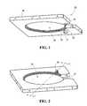
- FIG. 2is a lower perspective view of a spring drum and a support member of a supporting device of the apparatus shown in FIG. 1 ;
- FIG. 3is a cross-section of the supporting device shown in FIGS. 1 and 2 ;
- FIG. 4is a cross-section of the workpiece shown in FIGS. 1-3 supported in a heat-treating chamber by a plurality of the supporting devices shown in FIGS. 1-3 ;
- FIG. 5is a partial side elevation view of a workpiece and an apparatus for supporting the workpiece according to a second embodiment of the invention
- FIG. 6is a lower perspective view of an apparatus for supporting a workpiece according to a third embodiment of the invention, including a support member engageable with a workpiece and an actuator co-operating with the support member;
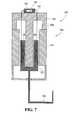
- FIG. 7is a simplified cross-section view of a voice coil actuator for co-operating with the support member shown in FIG. 6 ;
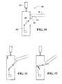
- FIG. 8is a simplified side elevation view of an apparatus for supporting a workpiece according to a fourth embodiment of the invention, including a moving member of an actuator co-operating with a motion translator to impart an arcuate motion to the support member shown in FIG. 6 ;
- FIG. 9is a simplified side elevation view of the moving member, motion translator and support member shown in FIG. 8 , shown in a second position;
- FIGS. 10-12are simplified partial side elevation views of an apparatus for supporting a workpiece, according to a fifth embodiment of the invention.
- FIGS. 13-14are simplified partial side elevation views of an apparatus for supporting a workpiece, according to a sixth embodiment of the invention.
- FIG. 15is a side elevation view of a supporting device of an apparatus for supporting a workpiece, according to a seventh embodiment of the invention.
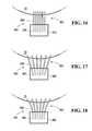
- FIG. 16is a partial bottom elevation view of a supporting device of an apparatus for supporting a workpiece, according to an eighth embodiment of the invention.
- FIG. 17is a partial bottom elevation view of a supporting device of an apparatus for supporting a workpiece, according to a ninth embodiment of the invention.
- FIG. 18is a partial bottom elevation view of a supporting device of an apparatus for supporting a workpiece, according to a tenth embodiment of the invention.
- FIG. 19is a side elevation view of the supporting device shown in FIG. 16 ;
- FIG. 20is a partial side elevation view of a supporting device of an apparatus for supporting a workpiece, according to an eleventh embodiment of the invention.
- FIG. 21is a perspective view of a workpiece and a supporting device, of an apparatus for supporting the workpiece, according to a twelfth embodiment of the invention.
- FIG. 22is a cross-section of the supporting device shown in FIG. 21 ;
- FIG. 23is a perspective view of a workpiece and a support system of an apparatus for supporting the workpiece, according to a thirteenth embodiment of the invention.
- FIG. 24is a partial bottom elevation view of a supporting device of the support system shown in FIG. 23 ;
- FIG. 25is a top elevation view of a workpiece and a support system for supporting the workpiece, according to a fourteenth embodiment of the invention.
- FIG. 26is a top perspective view of the workpiece and support system shown in FIG. 25 ;
- FIG. 27is a cross-section of the workpiece and support system shown in FIG. 25 .
- FIG. 28is a detail of the cross-section of the workpiece and the support system shown in FIG. 27 ;
- FIG. 29is a bottom elevation view of the workpiece and the support system shown in FIG. 25 ;
- FIG. 30is a rear elevation view of a support member clamp of the support system shown in FIGS. 25-29 ;
- FIG. 31is a partial cross-section of a support system of an apparatus for supporting a workpiece according to a fifteenth embodiment of the invention.
- FIG. 32is a partial cross-section of a support system of an apparatus for supporting a workpiece according to a sixteenth embodiment of the invention.
- FIG. 33is a front elevation view of a lateral supporting device of the support system shown in FIG. 32 , in a direction radially outward from a center of a workpiece plane plate aperture;
- FIG. 34is a partial cross-section of a supporting device of an apparatus for supporting a workpiece according to a seventeenth embodiment of the invention.
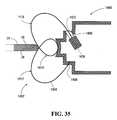
- FIG. 35is a partial cross-section of a support system of an apparatus for supporting a workpiece according to an eighteenth embodiment of the invention.
- FIG. 36is a cross-section of the workpiece shown in FIGS. 1-3 supported in a heat-treating chamber by a plurality of the supporting devices shown in FIGS. 1-3 , the chamber being modified in accordance with a nineteenth embodiment of the invention;
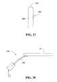
- FIG. 37is a side elevation view of a support member of an apparatus for supporting a workpiece, according to a twentieth embodiment of the invention.
- FIG. 38is a partial side elevation view of a supporting device of an apparatus for supporting the workpiece, according to a twenty-first embodiment of the invention.
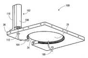
- FIG. 1an apparatus for supporting a workpiece according to a first embodiment of the invention is shown generally in FIG. 1 .
- the apparatusincludes a support system 20 configured to support a workpiece 24 while allowing thermally-induced motion of the workpiece.
- the support system 20includes a supporting device shown generally at 21 . More particularly, in this embodiment the supporting device 21 includes a support member 22 engageable with the workpiece 24 . More particularly still, in the present embodiment the support member 22 has a moveable engagement portion 52 shown in FIG. 3 , which is engageable with the workpiece 24 and which is moveable to allow the thermally-induced motion of the workpiece while supporting the workpiece.
- the moveable engagement portion 52 of the support member 22includes a tip of the support member.
- the support member 22is rigid, and the moveable engagement portion 52 is moveable by virtue of the support member 22 being pivotally moveable, as described in greater detail below.
- the moveable engagement portion 52may be moveable in other ways, such as those described in connection with the further embodiments described herein, for example.
- the workpiece 24includes a semiconductor wafer, and the moveable engagement portion 52 is engageable with the semiconductor wafer to allow the thermally-induced motion of the wafer while supporting the wafer. More particularly, in this embodiment the semiconductor wafer has a top-side or device side 26 , and a back-side or substrate side 28 .
- the support system 20includes a plurality of moveable engagement portions 52 of a plurality of respective support members 22 .
- the workpiece 24i.e. the semiconductor wafer
- the plurality of moveable engagement portionsincludes at least three moveable engagement portions of at least three respective support members, to provide stable support of the workpiece.
- the plurality of engagement portionsincludes at least four moveable engagement portions of at least four respective support members, so that stable support of the workpiece may be maintained even if one of the support members breaks or otherwise fails to function properly.
- the support systemis designed to allow the wafer to move freely and thus reduce wafer stress during the flash while secondarily dampening vibrations after the flash.
- the reaction force from the support members on the waferis achieved by employing moveable engagement portions with minimized mass, while in other embodiments, reaction forces may be minimized in other ways, such as by actively moving the supports, for example.
- each support member 22includes a support pin.
- the plurality of moveable engagement portions 52 of the plurality of support members 22comprises a plurality of tips of a plurality of respective support pins.
- the plurality of support pinsinclude material that is transparent to at least some irradiance wavelengths with which the workpiece 24 is capable of being irradiance-heated.
- the plurality of support pinsinclude optically transparent material.
- the support pinsinclude quartz support pins.
- quartzis a particularly suitable material for the support pins of the present embodiment (in which the workpiece is a semiconductor wafer to be heated by irradiance), due to its low thermal conductivity, its transparency, its non-contaminating nature, its good thermal stability, and its rigidity.
- the support pinsmay alternatively include sapphire, silicon nitrite, or silicon carbide, for example.
- other materialsmay be substituted, depending on the requirements of the application at hand.
- each of the moveable engagement portions 52 of the support members 22is resiliently engageable with the workpiece 24 .
- the support system 20further includes a plurality of force applicators in communication with the plurality of support members 22 to apply forces thereto to cause each of the engagement portions 52 to tend to maintain contact with the workpiece 24 during the thermally-induced motion of the workpiece. More particularly, as discussed in greater detail below, each of the force applicators includes a spring 48 connected to a respective one of the support members 22 .
- the workpiece plane plate 30is connected to a support member housing 36 of the supporting device 21 , to which the support member 22 is pivotally connected.
- the workpiece plane plate 30is also connected to a spring assembly 38 , which includes the spring 48 to which the support member 22 is connected.
- the supporting device 21is shown in greater detail.
- the support member 22is pivotally connected to the support member housing 36 .
- a pivot pin 40which in this embodiment includes a stainless steel dowel pin, is connected to opposite internal walls of the support member housing 36 , and extends through a hole formed in one end of the support member 22 .
- the spring assembly 38includes a spring drum 42 , which in this embodiment includes teflon. Alternatively, other materials, such as stainless steel for example, may be substituted.
- the spring drum 42is housed within a spring drum housing 44 , and is mounted to the workpiece plane plate 30 by a spring holder bracket 46 .
- the spring drum 42is used to mount the spring 48 , which in this embodiment includes a constant force spring.
- the force applicatoracts as a torque applicator.
- the spring 48is connected to a link 50 , which in this embodiment is composed of stainless steel.
- the link 50is pivotally connected to the support member 22 , at a location on the support member interposed between a pivot point (at the location of the pivot pin 40 ) of the support member 22 and the engagement portion 52 at which the support member 22 contacts the workpiece 24 .
- the torque applicator, or more particularly the spring 48applies an upward force at the location at which the link 50 is connected to the support member 22 .
- the constant force supplied by the spring 48and the forces supplied by the constant force springs of the other supporting devices similar to the supporting device 21 , are selected so that the cumulative constant upward force applied by the supporting members to the workpiece balances the downward force of gravity on the workpiece.
- the moveable engagement portions 52 of the support members 22which in this embodiment include the tips of the support pins, contact the lower side or substrate side 28 of the workpiece 24 to support the workpiece. More particularly, in this embodiment the tips of the support pins are engageable with an outer perimeter zone of the workpiece, or more particularly, with an outer “exclusion zone” or waste region, that is not used to manufacture semiconductor chips.
- the supporting device 21and the other similar supporting devices (such as the exemplary supporting devices 32 and 34 ), are used to support the workpiece 24 within a heat-treating chamber 60 .
- the chamber 60is similar to a heat-treating chamber disclosed in the aforementioned U.S. Patent Application Publication No. 2002/0102098, for thermal annealing of the device side 26 of the workpiece 24 .
- the workpiece plane plate 30including the supporting device 21 and the similar supporting devices 32 and 34 , are mounted in a middle region of the chamber 60 .
- the heat-treating chamber 60includes a heating system configured to heat a surface of the workpiece 24 relative to a bulk of the workpiece to cause the thermally-induced motion of the workpiece. More particularly, in the present embodiment the heating system includes an irradiance system configured to irradiate the surface of the workpiece. In this embodiment the irradiance system includes a pre-heating device 62 and a heating device 64 .
- the pre-heating device 62which may include an arc lamp or an array of arc lamps for example, irradiates the workpiece through a water-cooled quartz window 63 , to pre-heat the workpiece to an intermediate temperature at a rate that is slower than a thermal conduction time through the workpiece, so that the entire workpiece is heated relatively uniformly to the intermediate temperature.
- the pre-heating devicemay pre-heat the workpiece at a rate of 250° C./sec to 400° C./sec, to an intermediate temperature of 600° C. to 1250° C., although these are merely illustrative examples.
- the irradiance systemis configured to irradiate the surface (in this case the device side 26 ) for a time period shorter than a thermal conduction time of the workpiece 24 , to heat the surface to a greater temperature than the bulk of the workpiece.
- the heating device 64is used to rapidly heat the device side 26 of the workpiece to a substantially higher annealing temperature, at a rate much faster than a thermal conduction time through the wafer, so that only the top-side surface region of the workpiece is heated to the final annealing temperature, while the bulk of the workpiece remains close to the relatively cooler intermediate temperature.
- the final annealing temperaturemay include a higher temperature in the range of 1050° C. to a temperature close to the melting point of silicon, such as 1410° C., for example.
- the irradiance systemor more particularly the heating device 64 thereof, includes a flash-lamp operable to irradiate the device side 26 through a second water-cooled quartz window 65 with a high-power flash having a relatively short duration, preferably on the order of about one millisecond or less, for example, to heat the device side 26 at a heating rate in excess of 10 5 ° C./sec.
- the flash lampincludes a liquid-cooled arc lamp.
- the flash lampincludes a double water-wall arc lamp similar to that disclosed in commonly-owned U.S. Pat. No.
- the support system 20is configured to support the workpiece 24 while allowing thermal bowing of the workpiece, or more particularly, to automatically allow motion of the tips of the support pins in response to the thermally-induced motion of the outer perimeter zone of the workpiece.
- the moveable engagement portions 52 of the support members 22are automatically moveable in response to such thermally-induced motion, by virtue of the springs 48 to which the support members 22 are connected.
- the outer edges of the workpiece and the support membersi.e.
- the support member 22 of the supporting device 21 and similar support members of similar supporting devicesare allowed to move downward, thereby preventing breakage of the support members due to the reduced reaction force between the support members and the workpiece, and also preventing the workpiece from launching itself upward.
- the resilient downward movability of the moveable engagement portions 52allows downward motion of the outer regions of the workpiece while maintaining a center of mass of the workpiece in a desired range, or more particularly, while minimizing motion of the center of mass of the workpiece.
- the movability of the engagement portions to allow such thermally-induced motion and deformationserves to minimize stress in the workpiece while at the same time supporting the workpiece during the thermally-induced motion.
- the thermal bowingtends to occur sufficiently rapidly that the workpiece overshoots its equilibrium shape, and then tends to vibrate or oscillate about the equilibrium shape.
- the upward force applied by the constant force spring 48 to the support member 22pulls the support member back up, tending to maintain contact with the outer edge of the workpiece.
- the outer edges of the workpieceare allowed to move up and down, while tending to maintain contact with the support member 22 (and similar support members), until the vibration subsides.
- the spring-driven upward and downward movement of the support members 22allows upward and downward motion of the outer regions of the workpiece while minimizing the motion of the center of mass of the workpiece and minimizing stress in the workpiece.
- a supporting deviceaccording to a second embodiment of the invention is shown generally at 80 .
- the supporting device 80includes a support member 82 , similar to the support member 22 discussed earlier herein.
- the support member 82is mounted to a support member housing (not shown) at a pivot point 84 , for pivotal motion thereabout.
- the supporting device 80includes a force applicator, or more particularly a torque applicator comprising a spring 86 , in communication with the support member 82 to apply a force to the support member to cause an engagement portion 88 to tend to maintain contact with the workpiece during thermally-induced motion thereof.
- the torque applicatoris configured to apply a downward force at a location on the support member 82 such that the pivot point 84 of the support member 82 is interposed between the location and the engagement portion 88 . More particularly, in this embodiment the pivot point 84 is interposed between a point at which the support member 82 is connected to the spring 86 , and a point of contact between the engagement portion 88 of the support member and the workpiece 24 . Therefore, unlike the configuration shown in FIG.
- the spring 86(which in this embodiment includes a constant force spring) applies a downward force on one end of the support member 82 , so as to provide a torque that counter-balances a torque applied by the weight of the workpiece 24 on the engagement portion 88 of the support member 82 .
- the system 100includes a supporting device 102 configured to support the workpiece 24 while allowing thermal bowing or other thermally-induced motion of the workpiece.
- the supporting device 102includes a support member 104 having a moveable engagement portion engageable with the workpiece 24 .
- the moveable engagement portionincludes a tip of the support member 104 .
- the support member 104is rigid, and the moveable engagement portion is moveable by virtue of the support member 104 as a whole being moveable, as described below.
- the support member 104is engageable with the exclusion zone at the outer perimeter of the substrate side 28 of the workpiece.
- the support member 104includes a quartz pin, for reasons similar to those discussed in connection with the first embodiment of the invention. Alternatively, other materials may be substituted.
- the system 100further includes a plurality of support members similar to the support member 104 , such as a support member 108 , for example.
- the system 100includes at least three such support members, for stably supporting the workpiece.
- four or more support membersare provided, so that stable support of the workpiece may be maintained even if one of the support members breaks or otherwise fails to function properly.
- the system 100includes a support member motion system configured to move the moveable engagement portions of the plurality of support members 104 in response to the thermally-induced motion of the workpiece 24 . More particularly, in this embodiment, in which the support members 104 are rigid, the system is configured to move the engagement portions by moving the support members 104 themselves. More particularly still, in this embodiment the support member motion system includes, for each of the support members 104 , a respective actuator 106 connected to the support member 104 , for controlling motion of the support member 104 .
- the system 100includes a plurality of actuators (not shown) similar to the actuator 106 , for actuating the respective support members.
- Each actuator 106is mounted to an upper surface of the workpiece plane plate 30 , by way of a mounting bracket such as that shown at 110 in FIG. 6 .
- the support member 104extends through a hole 112 defined through the workpiece plane plate 30 , into the actuator 106 .
- the actuator 106includes a voice coil actuator, which is connected to the support member 104 . More particularly, in this embodiment the actuator 106 includes a fixed member 120 mounted to the bracket 110 , and a moving member 122 that moves relative to the fixed member.
- the fixed member 120produces a magnetic field through the moving member 122 .
- the fixed member 120includes a permanent magnet 124 and a ferromagnetic member 126 .
- the moving member 122includes an electric wire coil 128 .
- the actuator 106further includes a power supply unit 130 operable to apply a voltage between opposite ends of the electric wire coil 128 , thereby producing an electric current in the coil. It will be appreciated that as a result of the electric current produced in the coil of the moving member 122 , the magnetic field produced by the fixed member 120 exerts a force on the moving member 122 , in a direction dependent upon the direction of the current. The magnitude of the exerted force is directly proportional to the magnitude of the current in the coil 128 .
- the moving member 122 of the actuator 106is connected to the support member 104 .
- the magnitude of the upward supporting force exerted by the support member 104 upon the outer edge of the substrate side 28 of the workpiece 24may be controlled by controlling the electric current in the coil 128 of the actuator 106 .
- the support member motion systemincludes at least one controller configured to apply an electric current to each of the actuators to move each of the support members, thereby moving the moveable engagement portions thereof.
- the at least one controllerincludes a plurality of controllers, each in communication with a respective one of the plurality of actuators 106 .
- each controllerincludes a combined detector/controller 132 , which also acts as a detector for detecting the thermally-induced motion of the workpiece.
- the detector/controller 132is in communication with the power supply unit 130 and the coil 128 of the actuator 106 .
- the detector/controllerdetects the thermally-induced motion of the workpiece by detecting an electric current in the coil 128 , and conversely, the controller moves the support member 104 by controlling the power supply unit 130 to apply an electric current to the coil 128 .
- each detector/controller 132includes a processor circuit. More particularly, in this embodiment each detector/controller includes a digital signal processor (DSP). Alternatively, the detector/controller 132 may include a microcontroller or a similar device, with or without a central processing unit (CPU), for example. Alternatively, other types of detectors or controllers may be substituted, and the detecting and controlling functions may be performed by either the same or by different components.
- DSPdigital signal processor
- CPUcentral processing unit
- controllerdevice
- detectorand “processor circuit” are intended to broadly encompass any type of device or combination of devices capable of performing the functions described herein or equivalent functions, including (without limitation) other types of microprocessors, microcontrollers, other integrated circuits, other types of circuits or combinations of circuits, logic gates or gate arrays, or programmable devices of any sort, for example, either alone or in combination with other such devices located at the same location or remotely from each other, for example.
- controllersare known to those ordinarily skilled in the art upon review of this specification, and substitution of any such other types of controllers, detectors or processor circuits is considered not to depart from the scope of the present invention as defined by the claims appended hereto.
- the detector/controller 132includes a program memory 134 , which acts as a computer-readable medium for storing instruction codes for directing the detector/controller 132 to perform the various functions described herein.
- the program memory 132is merely one example of such a computer readable medium.
- instruction codesmay be provided on a different medium such as a compact disc, a floppy diskette, a hard disk drive, a read-only memory, or a FLASH memory, to name but a few examples.
- instruction codesmay be provided as code segments of signals embodied in carrier waves or embodied in a communications or transmission medium, such as a local area network or a wide area network such as the Internet, for example, and may be received from remote devices.
- a plurality of supporting devices similar to the supporting device 102 shown in FIG. 6may be substituted for the supporting devices 21 , 32 and 34 within the heat-treating chamber 60 shown in FIG. 4 .
- the support member motion systemis configured to move the engagement portions of the support members 104 to minimize forces applied between the workpiece 24 and the engagement portions, as discussed in greater detail below.
- the detector/controller 132controls the power supply unit 130 to control the voltage applied to the leads of the coil 128 , to cause a constant current having a desired magnitude to flow in the coil 128 , thereby applying a corresponding constant upward force on the moving member 122 and thus on the support member 104 , which in turn applies the upward force to the outer edge of the substrate side 28 of the workpiece 24 .
- the desired magnitude of the currentis selected so that the constant upward forces applied to the workpiece by the support member 104 , and by the similar support members of the other supporting devices, precisely balance the downward force of gravity acting on the workpiece 24 .
- the workpiece 24may again experience rapid thermal bowing, as described earlier herein (depending on the brevity of the duration of the flash, and the magnitude of the difference between the intermediate temperature of the bulk of the workpiece and the final annealing temperature to which only the device side 26 is heated).
- each of the detector/controllers 132is configured to detect, in its respective actuator 106 , an electric current resulting from a force applied to the engagement portion of the respective support member 104 by the thermally-induced motion of the workpiece.
- the detector/controller 132is configured to detect a deviation of the electric current in the coil 128 from a desired current level, the desired current level representing the above-noted constant current having the desired magnitude in order to precisely balance the gravitational force exerted on the support member by the workpiece.
- the detector/controllers 132Upon detecting the thermally-induced motion in the above manner, the detector/controllers 132 are configured to adjust positions of their respective support members 104 to maintain a difference between a weight of the workpiece 24 and an upward force applied to the workpiece by the engagement portions of the support members within a desired range. More particularly, each of the detector/controllers 132 is configured to minimize this difference. To achieve this, in the present embodiment, upon detecting the above-described deviation in the current level in the coil 128 resulting from the thermally-induced motion, the detector/controller 132 is configured to control the actuator 106 to adjust a position of the support member 104 to minimize the deviation.
- the detector/controller 132controls the power supply unit 130 to adjust the voltage applied to the leads of the coil 128 , to cause the actual current in the coil to return to the desired magnitude, thereby reducing the upward force applied by the support member 104 to the workpiece 24 , so that the support member 104 continues to counter-balance only the downward force of gravity on the workpiece, and does not counter-balance the additional downward force applied by the initial thermal deformation or bowing of the workpiece. Effectively, therefore, the support member 104 will be lowered, to allow the outer edge of the workpiece 24 to move abruptly downward as it initially bows.
- the thermal bowingtends to occur sufficiently rapidly that the workpiece overshoots its equilibrium shape, and then tends to vibrate or oscillate about the equilibrium shape.
- the detector/controller 132continues to apply the desired magnitude of current to the support member 104 (corresponding to an upward force that precisely balances the weight of the workpiece on the support member), but due to the upward thermal bowing motion of the edge of the workpiece, this upward force is no longer fully counter-balanced by the downward force applied by the workpiece to the support member, with the result that the support member 104 rises with the edge of the workpiece.
- the detector/controller 132quickly controls the power supply unit 130 to adjust the actual current in the coil so that the upward force applied by the support member 104 to the workpiece counter-balances only the force of gravity, thereby allowing the support member 104 to lower under the added force applied by the downward thermal bowing motion of the edge of the workpiece.
- the outer edges of the workpieceare allowed to move up and down, while tending to maintain contact with the support member 104 (and similar support members), until the vibration subsides.
- the actuator 106may include different types of actuators.
- the actuator 106may include a linear servo actuator.
- the actuator 106may include a piezoelectric actuator.
- piezoelectric actuatorsmay be advantageous due to their fast response times (typically at least as fast as 10 ⁇ 5 sec), precise movements, and significant available forces. However, most existing piezoelectric actuators are limited in their available ranges of motion, and for this reason may not be suitable for some applications.
- actuator 106may be substituted for other types of actuators.
- the support member motion systemis configured to move the support members in response to a detected parameter of the thermally-induced motion of the workpiece, namely, the detected change in electric current in the coil 128 produced by the change in the force applied to the support member 104 by the workpiece resulting from the thermally-induced motion.
- the motion systemmay be configured to move the support members in response to a predicted value of the thermally-induced motion. Such predicted values may be obtained empirically through observation of thermal processing of similar workpieces, for example.
- a single detector/controller 132may be employed for detection and control purposes for some or all of the actuators 106 .
- the moving member 122 of the actuator 106need not be connected directly to the support member 104 .
- the actuator 106may be connected to the support member 104 indirectly.
- the thermal bowing motion of the outer edge of the workpiece 24does not trace a vertical line, but rather, is more akin to an arc.
- the motion of the edge of the workpiecealso has a horizontal component.
- the outer edge of the workpiecemay be expected to travel horizontally inward by a distance on the order of one millimeter.
- the moving membermay be connected to the support member 104 via a motion translation device, for translating the vertical motion of the moving member into a motion of the support member 104 having both a vertical and a horizontal component.
- an actuator according to a fourth embodiment of the inventionis shown generally at 200 .
- the actuator 200is similar to the actuator 106 shown in FIG. 7 , and includes the moving member 122 and the fixed member 120 .
- the moving member 122is not directly connected to the support member 104 , but rather, is connected to a motion translator 202 .
- the motion translator 202is configured to translate a linear motion of a moveable member of the actuator 106 , or more particularly a linear motion of the moving member 122 , into an arcuate motion of the support member 104 .
- the motion translator 202includes a first connector arm 208 , to which the moving member 122 of the actuator 200 is rigidly connected.
- the motion translatorfurther includes a second connector arm 210 , to which the first connector arm 208 is pivotally connected.
- the second connector arm 210is pivotally connected to a first rigid bar 214 , at a first freely-movable pivot point 212 .
- the first rigid bar 214rigidly extends between a second freely-movable pivot point 215 and a first fixed pivot point 216 .
- the first freely-movable pivot point 212is disposed at a location along the first rigid bar 214 that is closer to the first fixed pivot point 216 than to the second freely-movable pivot point 215 .
- the first rigid bar 214is pivotally connected to a modified support member 204 at the second freely-movable pivot point 215 .
- the first fixed pivot point 216is connected to a housing (not shown) to prevent translational movement or displacement in any spatial dimension of the fixed pivot point 216 while permitting rotation of the first rigid bar 214 (and thus, permitting rotation of the pivot points 212 and 215 ) about the pivot point 216 .
- the motion translatorfurther includes a second rigid bar 218 , which is pivotally connected to the first fixed pivot point 216 and to a second fixed pivot point 220 , which is also locked to prevent translational movement or displacement of the pivot point 220 .
- the motion translator 202also includes a third rigid bar 222 connecting the second fixed pivot point 220 to a third freely-movable pivot point 224 disposed along the support member 204 .
- any vertical linear motion of the moving member 122 of the actuator 200causes the first and second freely-movable pivot points 212 and 215 to move in respective arcuate paths centered about the first fixed pivot point 216 , and likewise, causes the third freely-movable pivot point 224 of the support member 204 to move in an arcuate path centered about the second fixed pivot point 220 . Therefore, vertical linear motion of the moving member 122 of the actuator 200 causes a supporting tip 228 of the support member 204 to move along an arcuate path 230 shown in FIG. 9 .
- FIG. 9For ease of illustration, the dimensions of the various elements shown in FIG. 9 are not to scale, but rather, are exaggerated. The actual dimensions of these components will vary, to cause the arcuate path 230 traced by the tip 228 of the support member 204 to conform to the expected path of the outer edge of the workpiece 24 during thermal bowing. Alternatively, any other suitable type of motion translator may be substituted if desired.
- a system for supporting a workpiece according to a fifth embodiment of the inventionis shown generally at 300 in FIG. 10 .
- each of the plurality of moveable engagement portions of the plurality of support membersis resiliently engageable with the workpiece, in a manner similar to that shown in FIG. 5 .
- a support member motion system similar to that shown in FIGS. 6 and 7is configured to move the plurality of support members in response to the thermally-induced motion of the workpiece 24 .
- the system 300includes a plurality of supporting devices, including a first supporting device 302 shown in FIG. 10 , which is similar to the supporting device 80 shown in FIG. 5 .
- each supporting device 302includes a support member 304 having a pivot point 306 , about which the support member 304 may pivot.
- a respective spring 308is connected to each support member 304 at a location other than the pivot point 306 thereof.
- the pivot point 306is interposed between a point at which the support member 304 is connected to the spring 308 , and an engagement portion (a tip) 310 of the support member which contacts the workpiece 24 . Therefore, as with the configuration shown in FIG.
- the spring 308(which in this embodiment includes a constant force spring) acts as a torque applicator configured to apply a torque to the support member 304 about the pivot point 306 thereof to cause the engagement portion 310 to tend to maintain contact with the workpiece.
- the spring 308applies a downward force on one end of the support member 304 , so as to provide a torque that counter-balances a torque applied by the weight of the workpiece 24 on the engagement portion (tip) 310 of the support member 304 .
- the support member motion systemis configured to move the pivot points 306 of the support members 304 .
- the pivot point 306is not fixed in space relative to the rest of the chamber 60 , but rather, is connected to an actuator 320 .
- the connectionmay be direct, or alternatively, may be indirect (for example, the pivot point 306 may be provided by a pivot bar mounted between opposing walls of a housing 312 , and a direct connection may be provided by connecting the pivot bar to the actuator, or alternatively, an indirect connection may be made by connecting the housing to the actuator 320 ).
- the actuator 320may include a voice coil actuator such as that described earlier herein, or alternatively, may include any other suitable type of actuator.
- the motion systemis configured to apply electric currents to each of the actuators 320 , to move the support members 304 connected thereto, thereby moving the pivot points 306 of the support members.
- the actuator 320is synchronized with the heating device 64 , so that approximately simultaneously with the commencement of the thermal bowing motion of the workpiece 24 resulting from the abrupt heating flash produced by the heating device 64 , the actuator 320 moves the entire supporting device 302 downward, thereby causing the support member 304 to also move downward simultaneously with the initial downward thermal bowing motion of the outer edge of the workpiece 24 , but without any significant pivoting of the support member 304 about the pivot point 306 .
- the magnitude of the downward motion of the supporting device 302may be pre-determined in response to a predicted value of the thermally-induced motion of the workpiece 24 , for example.
- the actuator 320includes a detector/controller (not shown) similar to that discussed above in connection with FIG.
- FIG. 11illustrates the configuration of the supporting device 302 following this initial motion caused by the actuator 320 .
- the support member 304begins to pivot about the pivot point 306 , such pivotal motion being resisted by the constant force spring 308 , in a manner similar to the embodiment shown in FIG. 5 .
- the actuatormay similarly produce an upward motion of the entire supporting device 302 , if desired.
- the upward and downward motion of the support member 304is provided in a partly passive manner by the spring 308 , and in a partly active manner by the actuator 320 .
- other types of hybrid active/passive supporting systemsmay be substituted if desired.
- motion translatorssuch as that described earlier herein may also be employed, so that the motion of the pivot point 306 caused by the actuator 320 traces an arcuate path corresponding to the expected path of the edge of the workpiece during thermal bowing.
- the system 400includes a first plurality of moveable engagement portions of a first plurality of respective support members engageable with a lower surface of the workpiece 24 , and also includes a second plurality of moveable engagement portions of a second plurality of support members engageable with an upper surface of the workpiece.
- the first and second pluralities of engagement portionsare respectively engageable with the lower and upper surfaces of the workpiece at an outer perimeter zone thereof, which in this embodiment is the outer exclusion zone of the workpiece.
- each of the first plurality of support membersincludes a support member 404 of a first supporting device 402 , which is somewhat similar to the supporting device 102 shown in FIG. 6 , and thus includes an actuator 406 .
- each of the second plurality of support membersincludes a suppressing member 414 of a suppression device 410 , which in turn includes an actuator 416 .
- the suppressing member 414 and the suppression device 410are somewhat similar to the supporting member 104 and the supporting device 102 shown in FIG. 6 , but are configured to engage the workpiece by contacting the device side 26 of the workpiece, in the outer exclusion zone thereof.
- the actuators 406 and 416are controlled by a controller 420 , in communication with force detectors (not shown) in each of the actuators.
- the controller 420receives signals from the force detectors representing forces applied by the workpiece 24 to the support member 404 and the suppressing member 414 during thermal bowing or other thermally-induced motion.
- the controller 420adjusts the relative positions and/or forces applied by the support member 404 and the suppressing member 414 , to maintain the supporting and suppressing members in contact with the outer exclusion zone of the workpiece during thermal bowing and resulting vibration of the workpiece, as shown in FIG. 14 , for example.
- the controller 420is configured to move the first plurality of engagement portions of the support members 404 to minimize a difference between a weight of the workpiece and a force applied between the first plurality of engagement portions and the workpiece, in a manner similar to that discussed above in connection with FIGS. 6-9 .
- the controller 420is configured to move the second plurality of engagement portions of the suppressing members 414 , to minimize a force applied between the workpiece and the second plurality of engagement portions.
- the controller 420detects deviations from these desired electric current levels, and controls the voltages supplied to the actuators 406 and 416 to move the support members 404 and the suppressing members 414 , to restore the electric current levels in the coils of the actuators to their respective desired levels.
- the force detectors and the controller 420should be shielded so as to minimize any electrical interference or noise that may result from the sudden discharge of the capacitor banks or other pulsed power supply that is used to power the heating device 64 to produce the flash to heat the device side 26 of the workpiece to its final annealing temperature.
- the action of the suppressing member 414 and actuator 416 under the direction of the controller 420assists in suppressing the vibration of the workpiece, thereby reducing the possibility that damage to the workpiece may result from such vibration.
- motion translatorssuch as that described earlier herein may also be employed for the supporting member and the suppressing member.
- a supporting deviceis shown generally at 500 in FIG. 15 .
- the supporting device 500is similar in some respects to the supporting device 80 shown in FIG. 5 , and thus includes a support member 502 similar to the support member 82 , pivotally mounted to a support member housing 503 at a pivotal axis 504 , for pivotal motion thereabout.
- the housing 503may include the workpiece plane plate 30 shown in FIGS. 1-4 , or alternatively, may include a separate housing such as the housing 36 shown in FIG. 1 , for example, if desired.
- the pivotal axis 504is interposed between a point 505 at which the support member 502 is connected to a spring 506 (which in this embodiment includes a constant force spring), and a point of contact between a tip 508 of the support member and the workpiece 24 .
- the support member 502which in this embodiment includes a quartz pin, is rigidly connected to a casing 510 , which in turn is pivotally connected at the pivotal axis 504 to first and second mounting members (one of which is shown at 512 ) on opposite sides of the casing, each of which is rigidly secured to the housing 503 .
- the supporting device 500 of the present embodimentincludes a force applicator in communication with the support member 502 to apply a force thereto, to cause the engagement portion of the support member 502 to tend to maintain contact with the workpiece during the thermally-induced motion thereof.
- the force applicatorincludes first and second torque applicators configured to apply first and second opposing torques to the support member 502 , the second torque acting to oppose overshoot by the support member 502 of an equilibrium position thereof.
- the first torque applicatorincludes the spring 506 , which applies a torque (in a clockwise direction as shown in FIG.
- the second torque applicatorincludes a second spring 520 , which in this embodiment is connected to the supporting device 500 at an end distal or opposite from the tip 508 of the support member 502 .
- the second spring 520includes a flexible elongated metal member extending from the supporting device 500 in a direction away from the workpiece 24 . When the workpiece 24 is at rest and the supporting device is at equilibrium, a distal end of the second spring 520 maintains contact with a rigid stopper 522 protruding upward from a lower surface of the housing 503 .
- the support member 502pivots (in a direction counter-clockwise shown in FIG. 15 ) relative to the housing 503 , and accordingly, the distal end of the second spring 520 rises upward away from the stopper 522 along a counterclockwise arcuate path.
- the force applied to the supporting device 500 by the first spring 506causes the support member 502 to pivot in a clockwise direction, until the second spring 520 contacts the stopper 522 and bends as the supporting device overshoots its equilibrium angular position, thereby applying a counterclockwise torque to the supporting device to cause it to tend to return toward its equilibrium angle.
- the stopper 522 in this embodimentprevents the supporting device 500 from rotating clockwise too far past its equilibrium angular position.
- the second spring 520engages the stopper 522 in a resilient manner to achieve this, deleterious effects that would have otherwise have occurred (such as particle contamination that would have resulted from an abrupt collision between a rigid portion of the supporting device and the stopper) are minimized or avoided.
- a supporting deviceaccording to an eighth embodiment of the invention is shown generally at 600 .
- the supporting device 600includes a plurality of flexible support members shown generally at 602 .
- each of the flexible support members 602has a constrained portion such as that shown at 604 , and an unconstrained portion such as that shown at 606 .
- the moveable engagement portion of each of the support members 602includes the unconstrained portion 606 .
- each of the flexible support members 602includes a flexible fiber. More particularly, in this embodiment each of the flexible fibers includes an optical fiber. More particularly still, in the present embodiment each of the flexible fibers includes a quartz optical fiber.
- optical fiberswere selected due to their widespread availability, low cost and adequate mechanical properties, although some optical fibers may be undesirably brittle for certain applications. Alternatively, however, other types of fibers may be substituted. For example (without limitation), fibers composed of sapphire, crystalline quartz covered with amorphous quartz, silicon carbide, carbon fiber, metal-in-quartz, glass, or metal-in-glass, may be substituted.
- sapphire fiberstypically have greater strength than quartz, and may be advantageous for embodiments such as the present embodiment, in which an outer cladding of the fiber has been removed or is otherwise not present, as discussed in greater detail below.
- other types of flexible support membersmay be substituted.
- suitable flexible support membersshould be non-contaminating, flexible, low-mass, and should possess adequate temperature survivability to withstand the thermal cycles described herein.
- optical fibersare typically sold with an outer aluminum coating or cladding.
- the aluminum coatinghas been chemically removed from the distal ends of the unconstrained portions of the flexible support members 602 (“distal” meaning distal from the casing 610 ). More particularly, in this embodiment the aluminum cladding has been removed along a length of 2 mm from the distal end of each of the unconstrained portions 606 .
- the unclad distal end of each of the unconstrained portions 606preferably has a smooth surface, such as the smooth surfaces discussed below in connection with FIG. 37 , for example.
- the supporting device 600includes at least one constrainer configured to constrain the constrained portions 604 of the flexible support members 602 . More particularly, in this embodiment the at least one constrainer includes a casing 610 of the supporting device 600 .
- each of the constrained portions 604has a length of 10 mm, and is constrained or locked in position within the casing 610 .
- each of the unconstrained portionshas a length of 17 mm, of which 15 mm is aluminum-clad and the remaining 2 mm is the unclad distal end.
- each of the unconstrained portions 606extends from the casing 610 so that the unclad distal end of each unconstrained portion 606 engages the workpiece 24 in its outer exclusion zone.
- each of the flexible support members 602has a diameter of less than 2 mm.
- other dimensions or combinations of dimensionsmay be substituted in a particular embodiment.
- the dimensionswill be selected to provide the desired balance of flexibility and sufficiently fast response time.
- a larger diametertypically tends to increase the stiffness of the support member.
- Lengthening the unconstrained portion of the support membermay serve to decrease its stiffness and thus allow for a thicker diameter, although this approach tends to slow the response time constant of the support member, which is also undesirable in the present embodiment.
- the diameterwill be sufficiently small and the unconstrained length sufficiently long to provide the desired resiliency or flexibility, while the length should also be sufficiently short to provide a fast response time to allow the flexible support members to react to workpiece movements on a time scale on the order of a millisecond or less, while at the same time achieving these goals with a minimum mass of the unconstrained portion.
- the frequency of vibration of a support memberis related to its physical dimensions and mass as follows:
- the supporting device 600 shown in FIGS. 16 and 19is somewhat similar to the supporting device 500 shown in FIG. 15 , the most significant difference being the substitution of the flexible support members 602 (in this embodiment, flexible quartz fibers) for the rigid support member 502 .
- the present embodimentincludes a plurality of force applicators configured to apply forces to the plurality of supporting devices 600 to cause each of the unconstrained portions 606 to tend to maintain contact with the workpiece 24 during the thermally-induced motion of the workpiece. More particularly, the force applicators comprise torque applicators, or more particularly, the springs 506 and 520 .
- a support systemincludes a plurality of supporting devices similar to the supporting device 600 , disposed at various intervals around the outer perimeter of the workpiece 24 .
- the at least one constrainerincludes a plurality of constrainers, i.e. the plurality of casings 610 of the respective supporting devices 600 , disposed around the outer perimeter of the workpiece.
- the plurality of constrainersconsists of fewer constrainers than the number of the flexible support members, and each of the constrainers is configured to constrain more than one of the flexible support members, such as the set of six support members 602 shown in FIG. 16 , for example.
- each of the constrainers, i.e. each of the casings 610is configured to constrain the more than one of the flexible support members generally parallel to each other.
- a supporting deviceis shown generally at 650 in FIG. 17 .
- the supporting device 650is generally similar to the supporting device 600 , and includes a plurality of flexible support members shown generally at 652 , each of which has a constrained portion such as that shown at 654 , and an unconstrained portion such as that shown at 656 .
- Each of the constrained portionsis constrained or locked in position within constrainer, or more particularly, within a casing 660 .
- each constrainerconstrains more than one of the flexible support members 652 .
- each constraineris configured to constrain the more than one of the flexible support members generally divergent from each other.
- the flexible support members 652are not generally parallel, but rather, extend from the casing 660 toward the workpiece 24 in a divergent manner.
- the flexible support membersare generally straight (but may include curved end regions as discussed in greater detail below in connection with FIG. 20 ), and extend from the casing 660 along outwardly diverging paths.
- the flexible support membersmay diverge by extending along respective curved paths.
- a supporting device according to a tenth embodiment of the inventionis shown generally at 680 in FIG. 18 .
- the supporting device 680is generally similar to the supporting device 650 , and includes a plurality of flexible support members shown generally at 682 , each of which has a constrained portion such as that shown at 684 , and an unconstrained portion such as that shown at 686 .
- Each of the constrained portionsis constrained or locked in position within a casing 690 .
- the flexible support members 682extend from the casing 690 toward the workpiece 24 along respective divergent curved paths.
- the plurality of flexible support members 682may be pre-heated and bent into the desired curvature.
- each constrainermay constrain a constrained portion of only a single respective corresponding one of the flexible support members.
- the flexible support members 602 of the supporting device 600may be employed in other embodiments of the invention, such as any of the other embodiments described herein, for example.
- Embodiments such as those shown in FIGS. 17 and 18tend to allow a broader distribution of contact points with the workpiece, and reduce shadowing effects.
- a support system for resiliently supporting the workpieceincludes a plurality of support devices similar to the supporting device 600 (or alternatively, 650 or 680 ), disposed at various angular positions around the outer edge of the workpiece. Although three, or even two, such supporting devices may suffice for some applications, such a system preferably includes four or more such supporting devices, to provide adequate stability of support in the event that one of the supporting devices may fail to properly engage the workpiece.
- the flexible support members 602engage the outer exclusion zone of the workpiece at an angle of approximately 25° relative to the plane of the workpiece. Alternatively, other angles may be substituted.
- the flexible support members 602may engage the outer exclusion zone of the workpiece at steeper angles, such as the angle of engagement between the unconstrained portion 606 of the flexible support member 602 and the workpiece 24 shown in FIG. 20 , for example.
- the unconstrained portion 606 of each of the flexible support members 602preferably has a curved end region 620 for engaging the outer exclusion zone of the workpiece 24 .
- Such curvaturemay be achieved by pre-heating the flexible support member and mechanically bending the end region 620 while it is heated, for example.
- the curvature of the end region 620serves to minimize scraping of the substrate side of the workpiece by the end region 620 that might otherwise occur during thermal bowing and vibration of the workpiece.
- a support system for supporting the workpiece 24 according to a twelfth embodiment of the inventionis shown generally at 700 .
- the support system 700includes a plurality of supporting devices 701 such as those shown at 702 , 704 , 706 and 708 for example, disposed at various intervals around an inner workpiece support aperture of a workpiece plane plate 710 .
- the supporting device 702 and other similar supporting devicesextend inwardly and upwardly from a lower region of the workpiece plane plate 710 , to resiliently engage the outer exclusion zone of the substrate side 28 of the workpiece 24 .
- the supporting device 702is shown in greater detail in FIG. 22 .
- the supporting device 702includes a flexible support member 712 , which in this embodiment includes a quartz optical fiber, although alternatively, other suitable flexible support members may be substituted, as discussed earlier herein.
- the flexible support member 712is partly contained within a cladding layer 714 , which in this embodiment is the aluminum cladding layer in which the quartz fiber is commercially sold.
- the aluminum cladding layerhas been chemically removed from an unclad end region 716 of the flexible support member 712 distal from the workpiece plane plate 710 (proximal to the workpiece 24 ), so that the exposed or unclad end region 716 of the quartz fiber contacts the outer exclusion zone of the substrate side 28 of the workpiece 24 .
- the end region 716 of the flexible support member 712is curved, to minimize scraping of the substrate side 28 of the workpiece by the flexible support member during thermally-induced bowing and vibratory motions of the workpiece.
- the aluminum cladding layeris tightly secured within a casing 718 , which in this embodiment includes a stainless steel tube.
- the casing 718is tightly secured within the workpiece plane plate 710 .
- the flexible support member 712has a length of 27 mm, of which an end region proximal to the workpiece plane plate 710 having a length of 10 mm is encased within both the cladding layer 714 and the casing 718 , a middle region having a length of 13 mm is encased only within the cladding layer 714 , and the end region 716 distal from the workpiece plane, which has a length of 4 mm, is exposed, surrounded by neither the casing nor the cladding layer.
- the casing 718 and cladding layer 714extend from the workpiece plane plate 710 at an angle of 35° from the vertical (or 55° relative to the workpiece plane), although this angle was selected primarily for convenience to minimize the modifications required to the workpiece plane plate. Alternative angles are discussed in greater detail below. More generally, other combinations of dimensions, angles or configurations may be substituted, as desired.
- the support system 700includes a plurality of supporting devices such as the supporting device 702 shown in FIGS. 21 and 22 , disposed at various locations around the workpiece plane plate. More particularly, in the present embodiment the workpiece support system 700 includes 16 such supporting devices, arranged in eight closely-spaced pairs, each pair disposed symmetrically around the circumference of the workpiece 24 at 45° intervals.
- the placement of such supporting devices in closely-spaced pairs at each angular positioneffectively provides a back-up, so that if one of the pair of supporting devices fails to operate as intended, the other supporting device of the pair will generally be able to adequately support the workpiece at that angular position, thereby preventing the workpiece from falling or being damaged.
- a modified workpiece support system 700includes 6 such supporting devices 702 , arranged in three closely-spaced pairs, each pair disposed symmetrically around the circumference of the workpiece 24 at 120° intervals.
- a modified workpiece support system 700includes 8 such supporting devices 702 , arranged in four closely-spaced pairs, each pair disposed symmetrically around the circumference of the workpiece 24 at 90° intervals.
- the supporting devices 702 of these alternative embodimentsare similar to those shown in FIG.
- the exposed or unclad end region 716has a length of 2 mm.
- a shortening of the length of the unclad end region 716has been found to reduce the likelihood of fiber breakage.
- the shortened unclad end regions 716have smooth-surfaced tips, as described below in connection with FIG. 37 .
- each of the engagement portionsis engageable with the lower surface of the workpiece 24 at an angle of 10 to 80 degrees relative to a plane of the workpiece. More particularly, in these embodiments the angle is 15 to 35 degrees. More particularly still, in these alternative embodiments the angle is 25 degrees.
- an engagement angle that is steepsuch as 80 to 90° for example, increases the likelihood of gouging the wafer and damaging the support members or the wafer
- angles that are shallowsuch as 0 to 10° for example, increase the likelihood of breakage of the flexible support members 712 .
- an angle of engagement in the range of 10 to 80° relative to the workpiece planewill be preferred; an angle of engagement of 15 to 35° will be more strongly preferred; an angle of engagement of 25° will be more preferable still for certain applications.
- other anglesmay be substituted.
- the unencased portion of the flexible support member 712i.e., the portion of the flexible support member 712 that extends beyond the casing 718 , to be precisely identical in length to the unencased portions of the other flexible support members used in a given system, to maintain consistent flexibility from support member to support member.
- each of the supporting devices 702it is preferable for each of the supporting devices 702 to engage the workpiece 24 at the same angle.
- a support system for supporting the workpiece 24 according to a thirteenth embodiment of the inventionis shown generally at 800 in FIG. 23 .
- the support system 800includes a plurality of supporting devices 802 such as those shown at 804 , 806 and 808 for example, disposed at various intervals around an inner workpiece support aperture of a workpiece plane plate 810 .
- the supporting devices 802extend inwardly and upwardly from a lower region of the workpiece plane plate 810 , to resiliently engage the outer exclusion zone of the substrate side 28 of the workpiece 24 .
- each supporting deviceincludes a flexible curved support member resiliently engageable with the exclusion zone of the workpiece.
- the supporting device 804includes a flexible curved support member 812 , which in this embodiment includes an optical quartz fiber, although alternatively, other types of flexible support members may be substituted.
- the flexible curved support member 812includes first and second spaced apart constrained portions, with an unconstrained portion extending in a curved path therebetween. More particularly, in this embodiment the first constrained portion includes a first end region 815 , the unconstrained portion includes a middle region 816 , and the second constrained portion includes a second end region 817 . The first and second constrained portions are thus at opposite ends of the support member 812 , and define the unconstrained portion therebetween.
- the first and second constrained portionsare affixed to the workpiece plane plate 810 to prevent motion of the constrained portions.
- the flexible curved support member 812is partly contained within a cladding layer 814 , which in this embodiment is the aluminum cladding layer in which the quartz fiber is commercially sold.
- the aluminum cladding layerhas been chemically removed from the middle region 816 of the flexible curved support member 812 , so that the exposed middle region 816 of the quartz fiber contacts the outer exclusion zone of the substrate side 28 of the workpiece 24 .
- the system 800includes first and second constrainers configured to constrain the first and second constrained portions (i.e. the first and second end regions 815 and 817 ) in spaced apart relation to cause the unconstrained portion (i.e. the middle region 816 ) to extend in a curved path therebetween.
- the first and second constrainersinclude first and second casings 818 and 819 .
- the aluminum cladding layer 814 surrounding the flexible curved support member 812is tightly secured within the first casing 818 , which in this embodiment includes a stainless steel tube.
- the aluminum cladding layer 814 surrounding the flexible curved support member 812is tightly secured within the second casing 819 , which includes a similar stainless steel tube.
- the casings 818 and 819are tightly secured within the workpiece plane plate 810 .
- each of the casings 818 and 819is similar to the casing 718 shown in FIG. 22 , and is similarly secured to the workpiece plane plate.
- the first and second constrainerswhich in this embodiment include the casings 818 and 819 , are configured to constrain the first and second constrained portions (i.e. the first and second end regions 815 and 817 ) to cause the unconstrained portion (the middle region 816 ) to extend along the curved path from the first constrained portion upwardly and inwardly toward the workpiece 24 to a region of contact therewith and to extend from the region of contact downwardly and outwardly to the second constrained portion.
- the flexible curved support member 812protrudes from the casing 818 and cladding layer 814 at the first end region 815 , and extends inwardly and upwardly along an approximately arcuate path toward the workpiece 24 , so that a center of the middle region 816 contacts and supports the outer exclusion zone of the substrate side 28 of the workpiece 24 .
- the flexible curved support member 812then continues to extend, from its center, downwardly and outwardly along the arcuate path, to the second end region 817 , where the cladding layer 814 surrounding the end region 817 is secured within the casing 819 .
- a tangent to the unconstrained portioni.e. a tangent to the middle region 816 at the center thereof
- a tangent to the middle region 816 at the center thereofis substantially parallel to a tangent to an outer circumference of the workpiece 24 in the vicinity of the region of contact.
- the angle of the arcuate path of the flexible curved support member 812is approximately 35° from the vertical, although again, this angle was chosen for convenience, to minimize modifications to an existing workpiece plane plate. Alternatively, other angles and configurations may be substituted.
- the flexible support member 812may extend from the first end region 815 for a length of 10-20 mm within the casing 818 , and may extend for a further length of 20-40 mm beyond the casing within the cladding layer 814 , and may extend for a further unclad length of 2-4 mm at a central region thereof, at which the flexible support member 812 contacts the workpiece 24 .
- the flexible support membermay then extend for a further length of 20-40 mm within the cladding layer 814 toward the second end region 817 , and extend for a further length of 10-22 mm within the casing 819 .
- the flexible support membermay have a diameter of 0.5 to 2 mm, for example. Alternatively, other lengths and diameters may be substituted if desired.
- the cladding layer 814may be omitted entirely if desired.
- the plurality of supporting devices 802includes at least four such supporting devices similar to the supporting device 804 , to provide adequately stable support in the event that one of the supporting devices breaks or otherwise fails. More particularly, in this embodiment the plurality of supporting devices 802 includes 20 such supporting devices. Alternatively, however, other numbers of supporting devices may be substituted if desired.
- a support system for supporting the workpiece 24 according to a fourteenth embodiment of the inventionis shown generally at 900 .
- the support system 900includes a plurality of flexible support members shown generally at 902 .
- each of the flexible support members 902includes a flexible fiber resiliently engageable with the workpiece.
- each of the flexible fibersincludes a quartz optical fiber, although alternatively, as discussed elsewhere herein, sapphire or other types of fibers, or more generally, other types of flexible support members, may be substituted.
- alternative flexible support membersshould be non-contaminating, flexible, low-mass, and should possess adequate temperature survivability to withstand the thermal cycles described herein.
- an exemplary flexible support memberis shown generally at 903 in FIG. 28 .
- the flexible support member 903has a constrained portion 904 , and an unconstrained portion 906 . More particularly, in the present embodiment the flexible support member 903 includes the constrained portion 904 at an end thereof, and the unconstrained portion 906 extends inwardly from the constrained portion 904 toward a central region of the workpiece 24 .
- the flexible support member 903includes a fiber 907 .
- a portion of the length of the flexible fiber 907is encased within an outer cladding layer 908 , which in this embodiment is an aluminum coating layer that is commercially sold with the fiber 907 .
- the aluminum coatinghas been chemically removed from a segment of the length of the unconstrained portion 906 of the flexible support members 903 . More particularly, in this embodiment the flexible support member 903 has a length of 65 mm, and the aluminum cladding or coating has been chemically removed from the innermost 40 mm of its length.
- the aluminum coating or cladding layermay be omitted entirely in some embodiments, such as embodiments in which the support members include sapphire.
- the support system 900includes at least one constrainer for constraining the constrained portion 904 .
- the at least one constrainerincludes a workpiece plane plate 920 . More particularly, in this embodiment the at least one constrainer includes a plurality of clamps defined within the workpiece plane plate, for clamping the constrained portions of the plurality of flexible support members 902 . More particularly still, in the present embodiment, each constrained portion 904 is constrained or locked in position within a clamp shown generally at 910 in FIGS. 28 and 30 .
- the clamp 910includes an upper clamping member 912 and a lower clamping member 914 .
- the upper clamping member 912has a generally planar lower surface
- the lower clamping member 914has a V-shaped groove or channel 916 defined in its upper surface, extending along the length of the lower clamping member 914 .
- the dimensions of the V-shaped groove 916are selected so that the flexible support member 903 can be inserted into the V-shaped groove 916 , such that when the lower surface of the upper clamping member 912 is pressed against the upper surface of the lower clamping member 914 , the outer cladding layer 908 is snugly secured between the lower surface of the upper clamping member 912 and the two surfaces of the V-shaped groove 916 , thereby preventing the portion of the flexible support member 903 that is secured within the clamp 910 from movement relative thereto.
- the clamp 910is oriented so that the V-shaped groove 916 , and hence the flexible support member 903 , point radially inward toward the center of the workpiece 24 .
- a plurality of clampssuch as that shown at 910 are defined by an upper clamping ring that effectively acts as a plurality of upper clamping members 912 , and a lower clamping ring with a plurality of V-shaped grooves defined therein, which effectively acts as a plurality of lower clamping members 914 .
- the upper and lower clamping ringsextend radially inward for a length of approximately 10 mm, in which the constrained portion 904 of each flexible support member 902 is snugly secured. Alternatively, other constrained lengths may be substituted if desired.
- the workpiece plane plate 920defines a plurality of workpiece support apertures in an inner surface thereof, and the constrained portions 904 are affixed to the workpiece plane plate 920 with the unconstrained portions 906 extending inwardly toward the workpiece through the workpiece support apertures. More particularly, in this embodiment each of the workpiece support apertures includes a vertical slot 918 defined in the inner surface of the workpiece plane plate 920 .
- the unconstrained portion 906 of the flexible support member 903protrudes inwardly toward the center of the workpiece 24 , through the vertical slot 918 , which slot allows the unconstrained portion 906 of the flexible support member 903 to move upward and downward relative to the workpiece plane plate 920 .
- an inner tip 924 of each unconstrained portion 906inwardly past an outer edge 922 of the workpiece 24 , so that the inner tip 924 is at a smaller radial distance from the center of the workpiece than the outer edge 922 of the workpiece. More particularly, in this embodiment the inner tip 924 extends approximately 10 mm further inward than the outer edge 922 of the workpiece, although alternatively, other length relationships may be substituted.
- the engagement portion of the support member 903includes an intermediate point 926 along the unconstrained portion 906 between the constrained portion 904 and the inner tip 924 .
- the unconstrained portion 906or more particularly the intermediate point 926 therealong, is engageable with the outer edge 922 of the workpiece, to contact and support the workpiece.
- the workpiece plane plate 920is configured to constrain the constrained portions 904 in a generally horizontal direction to cause the unconstrained portions 906 to extend generally horizontally inwardly toward the central region of the workpiece 24 while downwardly sagging.
- the flexible support member 903bends downward, so that the inner tip 924 of the flexible support member is vertically displaced by a “sag displacement” distance below the plane of the workpiece 24 .
- the plurality of flexible support members 902includes at least twenty elongated flexible support members. More particularly, the plurality of support members 902 includes at least fifty such support members. More particularly still, in this embodiment the plurality of support members 902 includes approximately 60 flexible support members similar to the exemplary support member 903 , disposed at roughly equidistant intervals around an inner workpiece support aperture defined in the workpiece plane plate 920 . In this embodiment, in which the workpiece is a semiconductor wafer and the flexible support members 902 are optical fibers as described above, the “sag displacement” typically ranges from about 3 mm to about 5 mm.
- the unconstrained portions 906are engageable with the outer edge 922 of the workpiece 24 at an angle of less than about 10 degrees downward relative to the plane of the workpiece.
- other sag displacement distances and anglesmay be tolerable or desirable, depending upon the particular application at hand.
- each of the flexible support members 902has a diameter of between approximately 0.4 mm and 2 mm.
- other suitable dimensionsmay be substituted, selecting length and diameter to provide the desired resiliency and fast response time for a given application.
- the inner tip 924 of the flexible support member 903 shown in FIG. 28may be provided with a curved end region similar to the curved end region 620 shown in FIG. 20 , to minimize the effects of possible scraping against the substrate side 28 of the workpiece 24 during thermally-induced bowing or vibration.
- a support system for supporting a workpieceis shown generally at 1000 .
- the support system 1000is configured to suppress vibration of the workpiece, or more particularly, to suppress at least one natural vibration mode of the workpiece, which in this embodiment includes the first and second natural vibration modes of the workpiece.
- the support system 1000includes first and second supporting devices shown generally at 1002 and 1004 .
- the supporting devices 1002 and 1004include respective flexible support members 1006 and 1008 , which in this embodiment include quartz fibers. More particularly, in this embodiment the quartz fibers are optical quartz fibers from which the aluminum cladding layer has been chemically removed, and have a diameter of approximately 100 microns.
- each of the flexible support members 1006 and 1008has first and second spaced apart constrained portions, with an unconstrained portion extending in a curved path therebetween. More particularly, the first and second constrained portions of the flexible support member 1006 respectively include a fixed end 1010 and an adjustable end 1014 , and similarly, the first and second constrained portions of the flexible support member 1008 respectively include a fixed end 1012 and an adjustable end 1016 .
- the fixed end 1010 of the flexible support member 1006is attached to a workpiece plane plate 1018 in the vicinity of the workpiece 24 , just below the plane of the workpiece 24 , and similarly, the fixed end 1012 of the flexible support member 1008 is attached to the workpiece plane plate just above the plane of the workpiece.
- the workpiece plane plate 1018acts as a first constrainer for constraining the fixed ends 1010 and 1012 of the flexible support members 1006 and 1008 .
- each support memberextends along the curved path between the constrained portions, such that a tangent to the unconstrained portion at a region of contact with the workpiece extends radially inward toward a center of the workpiece.
- the flexible support member 1006extends from its fixed end 1010 (in a counter-clockwise direction as shown in FIG. 31 ) along a generally loop-shaped path, and contacts and supports the substrate side 28 of the workpiece 24 in the vicinity of the outer exclusion zone of the workpiece.
- the flexible support member 1006continues along the loop-shaped path from the point of contact with the workpiece, looping around (counter-clockwise) and re-entering the workpiece plane plate 1018 through an aperture 1020 defined in the lower surface of the workpiece plane plate.
- the adjustable end 1014 of the flexible support member 1006enters and is secured in a length controller 1022 , which acts as a second constrainer for constraining the adjustable end 1014 of the flexible support member 1006 .
- the system 1000includes the length controller 1022 , which, in this embodiment includes a mechanical retractor, and which retractably constrains the second constrained portion (i.e. the adjustable end 1014 ) of the flexible support member 1006 .
- the retractoris configured to retract the second constrained portion to effectively shorten the unconstrained portion, and conversely, is configured to extend the second constrained portion to effectively lengthen the unconstrained portion.
- the length controller 1022is remotely controllable from outside a process chamber in which the workpiece plane plate 1018 is located, to lengthen or shorten the effective length of the flexible support member 1006 , thereby changing the shape and dimensions of the loop-shaped path in which it extends to resiliently support the workpiece.
- the flexible support member 1008extends from its fixed end 1012 along a generally loop-shaped path (in a clockwise direction as shown in FIG. 31 ), contacts the device side 26 of the workpiece 24 in the vicinity of the outer exclusion zone of the workpiece, and continues (clockwise) along the loop-shaped path to re-enter the workpiece plane plate 1018 through an aperture 1024 defined in an upper surface of the workpiece plane plate.
- the adjustable end 1016 of the flexible support member 1008enters and is secured in a length controller 1026 , similar to the length controller 1022 .
- the length controller 1026is remotely controllable from outside the process chamber in which the workpiece plane plate 1018 is located, to retract a sufficient length of the flexible support member 1008 to move the flexible support member 1008 completely out of a cylinder-shaped volume defined above the plane of the workpiece 24 , thereby allowing the workpiece 24 to be lowered into position to be supported by the first flexible supporting device 1002 , or to be raised back out of position when thermal processing is complete.
- the length controller 1026may be remotely controlled to extend a sufficient length of the flexible support member 1008 so that the loop-shaped path of the flexible support member 1008 contacts the device side 26 of the workpiece at the outer exclusion zone.
- the effective diameters of the generally loop-shaped paths of the flexible support members 1006 and 1008depend upon the material chosen for the support members, and upon the range of expected workpiece motion.
- the effective diameters of the generally loop-shaped pathsmay be between about 30 mm and 100 mm for some embodiments, although alternatively, other effective diameters may be substituted.
- the support system 1000to support the workpiece 24 for such thermal processing, includes a plurality of lower support devices identical to the support device 1002 , and a plurality of upper support devices identical to the supporting device 1004 , disposed at various intervals around the perimeter of the workpiece plane plate 1018 .
- the system 1000includes first and second pluralities of elongated flexible support members. The unconstrained portions of the first plurality of flexible support members are engageable with the lower surface of the workpiece 24 and the unconstrained portions of the second plurality of flexible support members are engageable with an upper surface of the workpiece 24 .
- the upper support devicesserve to enhance stability and suppress vibration of the workpiece 24 during the thermal cycles described herein.
- the first and second supporting devices 1002 and 1004co-operate to at least partly suppress the first and second natural vibration modes of the workpiece 24 .
- the supporting device 1004 and other similar upper supporting devicesmay be omitted if desired, leaving the workpiece to be supported by the supporting device 1002 and other lower supporting devices.
- a support system for supporting a workpieceis shown generally at 1200 .
- the support system 1200includes a lateral support member configured to laterally support the workpiece 24 .
- the system 1200includes a lateral supporting device 1202 for providing resilient lateral support to the workpiece 24 .
- the thermal cycles described hereinmay tend to produce asymmetrical thermal bowing or vibrational motion of the workpiece, for example, due to non-uniform heating of the device side 26 of the workpiece in response to the flash, or due to non-uniform responses of various (vertical) supporting devices such as those described earlier herein, for example.
- Such asymmetrical motionmay include lateral motion of the workpiece 24 relative to a workpiece plane plate such as that shown at 1204 , for example.
- a workpiece plane platesuch as that shown at 1204
- the effects of such a collisionmay include particle contamination, or other physical damage to the workpiece 24 .
- the lateral supporting device 1202includes a lateral support member 1206 configured to laterally support the workpiece 24 .
- the support member 1206includes a plurality of lateral support members, such as those shown at 1208 , 1210 and 1212 in FIG. 33 , for example, at respective positions relative to an outer edge of the workpiece 24 .
- each of the lateral support membersis resiliently engageable with the outer edge of the workpiece.
- each of the lateral support membersincludes a flexible fiber, which in the present embodiment includes an optical fiber.
- each of the support membersincludes a quartz fiber.
- sapphire fibers, other fibers, other types of flexible support members, or more generally, other types of lateral support membersmay be substituted.
- the lateral support member 1206is connected to a positioner 1214 , which in this embodiment includes an aluminum block.
- the positioner 1214is connected to the workpiece plane plate 1204 , and extends sufficiently far into the workpiece support aperture defined in the workpiece plane plate to position the lateral support member 1206 close to the outer edge of the workpiece 24 .
- the lateral support member 1206 and similar support members, which in this embodiment include flexible fibers,are positioned at an angle substantially normal to a plane of the workpiece 24 .
- the aluminum coating or cladding layer that is typically sold with optical quartz fibershas been chemically removed, so that at least the portions of the lateral support members 1208 , 1210 and 1212 that are likely to come into contact with the workpiece 24 are exposed quartz, and hence, non-contaminating.
- the workpiececontacts most of the lengths of the quartz fibers (other than the length segment secured within the positioner 1214 ), and therefore, in this embodiment the aluminum coating or cladding has been removed from the entire lengths of the fibers (if desired, the aluminum cladding may be retained along the length segment that is secured within the positioner 1214 ).
- other materials that are typically not sold with any such aluminum claddingsuch as sapphire for example, may be substituted for the quartz fibers.
- the lateral support member and the other similar lateral support membersmay have a length of approximately 20-40 mm (excluding the portion that is secured within the positioner 1214 ), and may have a diameter of 0.5-2 mm, for example.
- other suitable dimensionsmay be substituted for a given application.
- the support system 1200includes a plurality of lateral supporting devices similar to the lateral supporting device 1202 , positioned at various intervals around the perimeter of the workpiece support aperture defined in the workpiece plane plate 1204 .
- the system 1200may include between four and 20 such lateral supporting devices, although alternatively, other numbers may be substituted.
- Such lateral supporting devicesmay be used in conjunction with vertical supporting devices, such as any of the other supporting devices described herein, for example.
- a lateral support systemsomewhat similar to that shown in FIGS. 32 and 33 may be provided, in which one or more rigid support members are substituted for the lateral support member 1206 .
- one or more rigid quartz pinsmay be substituted for the flexible support member.
- Such embodimentsmay suffice to contain lateral motion of the workpiece, however, such embodiments may also result in damage to or breakage of the workpiece 24 , depending upon the lateral momentum of the workpiece relative to the rigid support member(s) when the former collides with the latter.
- a support system for supporting a workpiece according to a seventeenth embodiment of the inventionis shown generally at 1300 in FIG. 34 .
- the support system 1300includes a support member which acts as both a vertical and lateral support member, and which includes a moveable vertical support engagement portion engageable with a lower surface of the workpiece 24 , as well as a lateral support engagement portion engageable with an outer edge of the workpiece.
- the support memberincludes a supporting device 1302 , which is a modified version of the supporting device 702 shown in FIG.
- the moveable vertical support engagement portion of the supporting device 1302includes the flexible support member 712 , including the cladding layer 714 and the casing 718 in which the flexible support member is secured to the workpiece plane plate 710 .
- the lateral support engagement portion of the supporting device 1302includes a second flexible support member 1304 .
- the second flexible support member 1304is similar to the first flexible support member 712 , and therefore also includes an optical quartz fiber, although alternatively, as discussed earlier herein, other types of fibers, or more generally other types of flexible support members, may be substituted if desired.
- the vertical and lateral support engagement portionsare resiliently engageable with the workpiece.
- the second flexible support member 1304has a smaller diameter than the first flexible support member 712 . More particularly, in this embodiment the second flexible support member 1304 has a diameter of approximately 0.5 mm, whereas the first flexible support member 712 has a diameter of approximately 4 mm. Alternatively, however, other suitable dimensions may be substituted as desired.
- the second flexible support member 1304includes an outer cladding layer 1306 , which in this embodiment is the aluminum coating that is commercially sold with the optical quartz fiber.
- the aluminum coatinghas been chemically removed from at least a portion of the second flexible support member 1304 that may possibly come into contact with the workpiece 24 , to avoid contamination of the workpiece.
- the second flexible support member 1304extends for a length of 10-20 mm within the outer cladding layer 1306 , and extends unclad for a further length of 20-40 mm beyond the cladding layer, although alternatively, other suitable lengths may be substituted if desired.
- the second flexible support member 1304is secured to the first flexible support member 712 by a collar 1308 .
- the collar 1308may include stainless steel or titanium, for example, although alternatively, other suitable materials may be substituted.
- the second flexible support member 1304may be connected to the remainder of the supporting device 1302 in any other suitable manner.
- the supporting device 1302may include a retractor 1310 , connected to a portion of the second flexible support member 1304 , for retracting the second flexible support member 1304 toward the workpiece plane plate 710 , to allow insertion or removal of the workpiece 24 .
- the second flexible support member 1304may be pre-heated and pre-bent back toward the workpiece plane plate 710 , to avoid the need for such a retractor.
- such pre-heating and pre-bendingmay be combined with a retractor in a given embodiment, if desired.
- the support system 1300includes a plurality of supporting devices similar to the supporting device 1302 shown in FIG. 34 , disposed at various intervals around the inner workpiece support aperture defined in the workpiece plane plate 710 .
- the system 1300includes a plurality of support members including a plurality of vertical and lateral support engagement portions engageable with the workpiece.
- a support system for supporting a workpieceis shown generally at 1400 .
- the support system 1400includes a supporting device 1402 .
- the supporting device 1402includes a flexible support member 1404 , which in this embodiment includes an optical quartz fiber.
- other types of fibers, or more generally, other types of flexible support membersmay be substituted.
- the flexible support member 1404includes first and second spaced apart constrained portions, with an unconstrained portion extending in a curved path therebetween. More particularly, in this embodiment the first and second constrained portions include a fixed end 1406 , and an adjustable end 1408 .
- a workpiece plane plate 1410acts as a first constrainer for constraining the first constrained portion, i.e. the fixed end 1406 , which in this embodiment is attached to the workpiece plane plate 1410 in the vicinity of the workpiece 24 , just below the plane of the workpiece 24 .
- the unconstrained portion of the support member 1404extends along the curved path between the constrained portions, to form a first generally loop-shaped path segment 1412 extending from the first constrained portion below a plane of the workpiece 24 and contacting the workpiece at a lower surface thereof, a second generally loop-shaped path segment 1414 extending between an outer edge of the workpiece 24 and an inner edge of the workpiece plane plate 1410 , and a third generally loop-shaped path segment 1416 extending above the plane of the workpiece and contacting the workpiece at an upper surface thereof, the curved path terminating at the second constrained portion.
- the flexible support member 1404extends from its fixed end 1406 along the first generally loop-shaped path segment 1412 (in a clockwise direction as shown in FIG. 35 ) below the plane of the workpiece, contacting and supporting the substrate side 28 of the workpiece 24 in the vicinity of the outer exclusion zone of the workpiece.
- the flexible support member 1404then continues to extend (clockwise) through the second generally loop-shaped path segment 1414 defined between the outer edge of the workpiece 24 and an innermost portion of the workpiece plane plate 1410 .
- the flexible support member 1404then continues to extend (clockwise) through the third generally loop-shaped path segment 1416 extending above the plane of the workpiece, re-entering the workpiece plane plate through an aperture 1422 defined in the upper surface of the workpiece plane plate.
- the adjustable end 1408 of the flexible support member 1404enters and is secured in a second constrainer, which in this embodiment includes a length controller 1424 , similar to the length controllers 1022 and 1026 shown in FIG. 31 .
- the flexible support member 1404due to its configuration, and in particular to the generally loop-shaped path segments 1412 , 1414 and 1416 , provides both vertical and lateral resilient support to the workpiece 24 .
- this configuration of the flexible support member 1404also partly suppresses the first and second natural vibration modes of the workpiece 24 .
- the second constraineracts as a retractor configured to retract the second constrained portion, to move the third generally loop-shaped path segment 1416 out of a volume defined above the upper surface of the workpiece.
- the length controller 1424is remotely controllable from outside a process chamber in which the workpiece plane plate 1410 is located, to lengthen or shorten the effective length of the flexible support member 1404 , thereby changing the shape and dimensions of the loop-shaped path in which it extends to resiliently support the workpiece.
- the support system 1400includes a plurality of supporting devices identical to the supporting device 1402 , disposed at various intervals around the perimeter of the workpiece support aperture defined in the workpiece plane plate 1410 .
- the support systemmay include between four and 20 such supporting devices, and the flexible support members of such devices may range from 0.5-2 mm in diameter, and from 50 mm to 300 mm in length. Alternatively, other numbers of supporting devices and dimensions of flexible support members may be substituted, if desired.
- the second generally loop-shaped path segment 1414 defined by the flexible support member 1404may be attached to the workpiece plane plate 1410 , for additional stability. Alternatively, such attachment may be omitted if desired.
- a heat-treating chamberaccording to a nineteenth embodiment of the invention is shown generally at 1500 in FIG. 36 .
- the chamber 1500is similar to the chamber 60 shown in FIG. 4 , but has been modified to include an additional quartz window 1510 , mounted above and in close proximity to the device side 26 of the workpiece 24 . More particularly, in this embodiment the window 1510 is mounted approximately 1 cm above a plane of the workpiece 24 , although alternatively may be mounted at other distances from the workpiece, with a distance of 1 to 10 cm being preferred for the present embodiment.
- the window 1510is preferably cooled, and in this embodiment is gas-cooled, although alternatively may be cooled by water or other suitable liquids, depending on the wavelengths that the window is required to transmit for heating or measurement purposes.
- the pressure of process gases between the workpiece 24 and the window 1510provides resistance to vertical motion of the workpiece.
- the additional gas pressure between the workpiece 24 and the window 1510serves to oppose vertical motion of the workpiece 24 , thereby tending to minimize motion of a center of mass of the workpiece.
- the window 1510also tends to reduce convective heat loss from the device side of the workpiece, resulting in improved temperature uniformity.
- a similar effectmay be obtained without the window 1510 , by moving the existing window 65 closer to the device side 26 of the workpiece 24 .
- the plurality of moveable engagement portions of the plurality of support membersmay include a plurality of smooth-surfaced tips of a plurality of respective support pins.
- a supporting deviceis shown generally at 1600 .
- the supporting device 1600includes a support member 1608 having a smooth-surfaced tip 1610 .
- the smooth-surfaced tip 1610is ball-shaped or hemispherical, although alternatively, other smooth surfaces may be substituted.
- Such smooth-surfaced tipstend to reduce friction and scratching of the workpiece 24 .
- scratching between the support members and the lower surface of the workpiecemay cause undesirable particle contamination, and may also undesirably roughen the lower surface of the workpiece.
- Minimization of frictional forcesis desirable not only to lower stress from point loading to reduce or prevent local stress and scratching in the vicinity of the points of contact between the support members and the workpiece, but also to lower the total stress to which the workpiece is subjected during thermal processing as described herein.
- the support member 1608is made of quartz, or more particularly, of an optical quartz fiber similar to those described above in connection with other embodiments of the invention. More particularly still, in the present embodiment the smooth-surfaced tip 1610 of the support member 1608 is formed by using a laser to melt the tip of the support member, thereby forming a ball-shaped tip as the tip cools.
- the fiberis clad, such as the aluminum cladding of the unconstrained portion 606 of each flexible support member 602 shown in FIG. 16
- the aluminum claddingis preferably removed from the tip prior to laser-melting to form the smooth-surfaced tip 1610 .
- the claddingmay be chemically removed from a 2 mm length of the fiber in the vicinity of the tip prior to formation of the smooth-surfaced tip.
- the support member 1608may be made of other materials, such as sapphire or any of the materials described earlier herein, for example.
- the support member 1608may include metal.
- the support member 1608may include a support pin including tungsten, and at least the tip of the support pin may have an outer coating to reduce friction and scratching.
- the outer coatingmay include tungsten nitride or tungsten carbide, for example, although other types of coatings may be substituted. Or, as a further alternative, such coatings may be omitted.
- the tip of the support member 1608may be laser-melted to form a ball shape, in a manner similar to that described above in connection with quartz support members. Alternatively, other ways of achieving the desired smooth-surfaced tip 1610 may be substituted.
- Such smooth-surfaced support members 1608may be employed in or substituted for support pins or other support members in other embodiments of the invention.
- a supporting deviceaccording to a twenty-first embodiment of the invention is shown generally at 1700 in FIG. 38 .
- the supporting device 1700is similar to that shown in FIG. 20 .
- a modified support member 1702does not engage the workpiece 24 at the outer exclusion zone thereof, but rather, engages the workpiece at a further inward region, i.e., at a smaller radial distance from the center of the workpiece than the exclusion zone.
- the workpieceis supported by a plurality of similar support members whose moveable engagement portions engage the lower surface of the workpiece at a common radial distance from the center of the workpiece, at various angular intervals.
- the positions at which the moveable engagement portions of the support members engage the workpiecemay vary, depending on the particular application in question, the available resiliency or softness of the support members in question, and the desired balance between minimizing vertical launch of the wafer and suppressing higher-order vibrational modes of the workpiece resulting from the flash.
- the support pinsmay be positioned at an equilibrium radial, distance from the center of the wafer, so that the thermal bowing produces a downward momentum of the outer portion of the wafer outside the equilibrium radial distance that tends to balance the upward momentum of the central region of the wafer, so that the wafer does not launch itself upward from the support pins.
- the workpieceincludes a silicon semiconductor wafer having a radius of 150 mm, and having axis symmetric natural vibration modes at frequencies of approximately 113 Hz (mode 1 ), 476 Hz (mode 2 ), and 1007 Hz (mode 3 )
- setting the radial distance r for engagement of the moveable engagement portions of the support membersequal to approximately 104 mm minimizes the tendency of the workpiece to launch itself upward.
- this positioningalso tends to excite the second natural vibration mode of the wafer, which may tend to damage or even shatter the workpiece, depending upon the magnitude and rapidity of the device-side temperature jump.
- the modified support member 1702is formed of a transparent material, to minimize shadowing effects on the workpiece. More particularly, in this embodiment the transparent material is quartz. Alternatively, other materials may be substituted. In this embodiment, the modified support member 1702 is also reduced in size, to further reduce any remaining shadowing effects, and also to reduce its mass.
- thermal “bowing” and related oscillations or vibrationsare the primary sources of thermally-induced motion described in connection with the above embodiments of the invention, alternatively, other embodiments of the invention may be applied to address other types of thermally-induced motion.
- the thermally-induced motionmay include thermal bending
- the support systemmay be configured to support the workpiece while allowing the thermal bending of the workpiece.
- one recently proposed thermal processing methodinvolves securely holding a substrate to a stage, by mechanical clamps, electrostatic or vacuum chucks, or equivalent grasping devices.
- a continuous wave electromagnetic radiation sourceis used with focusing optics to produce a line of radiation on an upper surface of the substrate.
- a translation mechanismis then used to move the stage and the radiation source relative to one another, to cause the line of radiation to scan across the upper surface of the substrate.
- mechanical clamps or other such grasping devicesto securely hold the substrate to the stage prevents thermally-induced bending of the substrate. In the absence of such clamping, the substrate would tend to thermally bend along the line of radiation, in order to minimize its own internal stress. By preventing the substrate from bending, the use of such clamps or grasping devices causes increased thermal stress in the substrate, thereby increasing the likelihood of damage to or breakage of the substrate.
- support memberscomprising moveable engagement portions that are moveable to allow thermally-induced motion of the workpiece, such as the support members described above in connection with other embodiments of the invention, for example, may be substituted for the mechanical clamps or other grasping devices previously proposed for this particular thermal processing method.
- supporting devicessuch as the supporting device 402 shown in FIG. 13 may be provided to allow thermally-induced bending of the workpiece, thereby reducing internal stress in the workpiece as it is effectively scanned by the line of radiation.
- the controller 420may be re-programmed, to retain the support member 404 and the suppressing member 414 in fixed positions until after the line of radiation has passed over the location at which the support member 404 and suppressing member 414 engage the workpiece 24 , and to thereafter allow thermally-induced bending of the workpiece 24 .
- the relatively “cold” portion of the workpiece 24 which has not yet been heatedis maintained flat for subsequent heating by the line of radiation, while at the same time, stress in the workpiece 24 is minimized by allowing thermally-induced motion of the portion of the workpiece that has already been heated.
- the various support systemsare configured to absorb kinetic energy from the workpiece.
- the flexible support member embodiments described abovewhen the outer regions of the workpiece initially move downward during thermal bowing, thereby pushing the engagement portions of the support members downward and thus bending the support members, at least some of the kinetic energy of the workpiece is at least temporarily absorbed by the support members and stored as potential energy therein.
- a method of heat-treating a workpiecemay also be employed, preferably (although not necessarily) in conjunction with other embodiments of the invention disclosed herein.
- the methodincludes irradiating a surface of the workpiece during a time period having a duration less than a thermal conduction time of the workpiece and sufficient to allow at least some thermal bowing of the workpiece, to heat the surface to a desired temperature greater than that of a bulk of the workpiece. More particularly, in this embodiment the method includes irradiating the surface of the workpiece for a first time period less than the thermal conduction time of the workpiece, to heat the surface to an intermediate temperature greater than that of the bulk of the workpiece.
- the methodthen includes irradiating the surface for a second time period less than the thermal conduction time of the workpiece, to heat the surface to the desired temperature.
- the second time periodcommences within an interval following the first time period sufficient to allow at least some thermal bowing of the workpiece.
- the heating device 64which in the present embodiment includes a flash lamp, is used to irradiate the device side 26 surface of the workpiece 24 , during both the first and second time periods.
- the thermal conduction time of the workpiece 24is on the order of 10-15 ms
- the first time periodis on the order of 1 ms
- the second time periodis also on the order of 1 ms.
- the interval following the first time period (prior to commencement of the second time period)is on the order of several milliseconds.
- the irradiance systemor more particularly the heating device 64 which includes the flash lamp, is configured to impart more radiant energy to the surface of the workpiece during the second time period than during the first time period, and is also configured to commence the second time period within several milliseconds following the end of the first time period.
- the heating device 64may irradiate the device side 26 of the workpiece to deliver approximately 10 J/cm 2 of energy to the device side during a first time period of one millisecond, then deliver no energy to the device side during the following several-millisecond interval, and then irradiate the device side to deliver approximately 20 J/cm 2 of energy to the device side during a second time period of one millisecond.
- the workpiece 24is pre-heated by the pre-heating device 62 , which irradiates the substrate side 28 to pre-heat the workpiece 24 to an intermediate temperature.
- This pre-heatingoccurs at a rate that is slower than the thermal conduction time of the workpiece, such as 100° C./s to 400° C./s, for example.
- the first time periodduring which the device side 26 is first irradiated by the heating device 64 , commences as soon as the intermediate temperature is reached.
- such methodsmay serve to reduce thermal stress and suppress vibration in the workpiece.
- the workpiece 24has only just begun to thermally bow, and has therefore achieved only a relatively small percentage of its maximum thermal bowing amplitude.
- the maximum thermal bowing amplitudeis not achieved until several milliseconds later, at which time the workpiece has overshot its equilibrium shape. A millisecond or so later, the workpiece 24 is still significantly bowed but is returning toward its flat position with significant return velocity.
- the heating device 64subjects the device side 26 of the workpiece 24 to a second irradiance flash during the second time period of approximately 1 ms in duration.
- the interval between the first and second time periodsi.e., between the first and second heating flashes
- the stress in the workpiece produced by the thermal bowing resulting from the second flashis diminished, because the wafer is already thermally bowed due to the first flash.
- the thermal bowing resulting from the second flashalso acts in a direction opposite to the existing return velocity of the workpiece as it attempts to return toward its flat position. Accordingly, the thermal bowing resulting from the second flash tends to suppress residual vibrations from the first flash.
- the combination of two such flash-heating stages in rapid successionallows higher peak device side temperatures to be achieved, while suppressing residual vibrations in the workpiece.
- the irradiance systemmay be configured to continuously irradiate the device side surface of the workpiece for an interval shorter than a thermal conduction time of the workpiece and sufficiently long to allow at least some thermal bowing of the workpiece.
- the heating device 64may be operated to expose the device side 26 to a continuous irradiance pulse having a duration shorter than the 10-15 ms thermal conduction time of the workpiece but long enough to allow at least some thermal bowing of the workpiece.
- a pulsemay extend over multiple milliseconds, such as about six milliseconds, for example.
- the irradiance systemmay be configured to vary an intensity of irradiance during the interval. For example, this may include irradiating the surface with a greater intensity during a later portion of the interval than during an earlier portion of the interval, for example.
- the pulsemay be shaped so as to deliver more energy to the surface of the workpiece during the latter half of the pulse duration than during the former half of the pulse duration.
- a plurality of support membersmay include a plurality of flexible support members, each having a constrained portion and an unconstrained portion, as described above in connection with FIG. 16 , for example, and the moveable engagement portions may include the unconstrained portions.
- a support member motion systemas described above in connection with FIG.
- certain flexible support membersmay cause partial shadowing upon the workpiece 24 . This may result in non-uniform heating of the workpiece in the vicinity of such shadows.
- the use of optical fibers as flexible support membersmay be exploited, to convey additional irradiance from one or more irradiance sources (not shown) to the workpiece through the fibers themselves, to further irradiate the workpiece in the vicinity of such shadows, thereby reducing the non-uniformity of the irradiance field incident upon the workpiece.
Landscapes
- Engineering & Computer Science (AREA)
- Physics & Mathematics (AREA)
- Condensed Matter Physics & Semiconductors (AREA)
- General Physics & Mathematics (AREA)
- Manufacturing & Machinery (AREA)
- Computer Hardware Design (AREA)
- Microelectronics & Electronic Packaging (AREA)
- Power Engineering (AREA)
- Container, Conveyance, Adherence, Positioning, Of Wafer (AREA)
- Lining Or Joining Of Plastics Or The Like (AREA)
Abstract
Description
where
E=Young's Modulus [N/m2]
I=Area Moment of Inertia of Support Member Cross Section [m4]
t=Length of Support Member [m]
μ=Mass per Unit Length of Support Member [kg/m]
A=Coefficient (A=3.52 for vibrational mode2; A=22.0 for mode2; A=61.7 for mode3, etc.)
Claims (20)
Priority Applications (1)
| Application Number | Priority Date | Filing Date | Title |
|---|---|---|---|
| US13/359,857US8434341B2 (en) | 2002-12-20 | 2012-01-27 | Methods and systems for supporting a workpiece and for heat-treating the workpiece |
Applications Claiming Priority (4)
| Application Number | Priority Date | Filing Date | Title |
|---|---|---|---|
| US43467002P | 2002-12-20 | 2002-12-20 | |
| US46865903P | 2003-05-08 | 2003-05-08 | |
| US10/742,575US9627244B2 (en) | 2002-12-20 | 2003-12-19 | Methods and systems for supporting a workpiece and for heat-treating the workpiece |
| US13/359,857US8434341B2 (en) | 2002-12-20 | 2012-01-27 | Methods and systems for supporting a workpiece and for heat-treating the workpiece |
Related Parent Applications (1)
| Application Number | Title | Priority Date | Filing Date |
|---|---|---|---|
| US10/742,575ContinuationUS9627244B2 (en) | 2002-12-20 | 2003-12-19 | Methods and systems for supporting a workpiece and for heat-treating the workpiece |
Publications (2)
| Publication Number | Publication Date |
|---|---|
| US20120118867A1 US20120118867A1 (en) | 2012-05-17 |
| US8434341B2true US8434341B2 (en) | 2013-05-07 |
Family
ID=32685329
Family Applications (2)
| Application Number | Title | Priority Date | Filing Date |
|---|---|---|---|
| US10/742,575Active2035-08-19US9627244B2 (en) | 2002-12-20 | 2003-12-19 | Methods and systems for supporting a workpiece and for heat-treating the workpiece |
| US13/359,857Expired - Fee RelatedUS8434341B2 (en) | 2002-12-20 | 2012-01-27 | Methods and systems for supporting a workpiece and for heat-treating the workpiece |
Family Applications Before (1)
| Application Number | Title | Priority Date | Filing Date |
|---|---|---|---|
| US10/742,575Active2035-08-19US9627244B2 (en) | 2002-12-20 | 2003-12-19 | Methods and systems for supporting a workpiece and for heat-treating the workpiece |
Country Status (7)
| Country | Link |
|---|---|
| US (2) | US9627244B2 (en) |
| JP (1) | JP4988202B2 (en) |
| KR (2) | KR20120045040A (en) |
| CN (1) | CN1729554B (en) |
| AU (1) | AU2003287837A1 (en) |
| DE (1) | DE10393962B4 (en) |
| WO (1) | WO2004057650A1 (en) |
Cited By (4)
| Publication number | Priority date | Publication date | Assignee | Title |
|---|---|---|---|---|
| US11193178B2 (en) | 2017-08-16 | 2021-12-07 | Beijing E-town Semiconductor Technology Co., Ltd. | Thermal processing of closed shape workpieces |
| US20210402484A1 (en)* | 2016-06-17 | 2021-12-30 | Baker Hughes, A Ge Company, Llc | Tail stock for a long vertically suspended workpiece that will experience heat expansion |
| US11521868B2 (en) | 2018-03-20 | 2022-12-06 | Beijing E-Town Semiconductor Technology, Co., Ltd | Support plate for localized heating in thermal processing systems |
| KR20230041600A (en) | 2021-09-17 | 2023-03-24 | 가부시키가이샤 스크린 홀딩스 | Heat treatment susceptor and heat treatment apparatus |
Families Citing this family (28)
| Publication number | Priority date | Publication date | Assignee | Title |
|---|---|---|---|---|
| DE10297622B4 (en) | 2001-12-26 | 2018-06-14 | Mattson Technology Inc. | Temperature measurement and methods and systems for heat treatment |
| WO2004057650A1 (en) | 2002-12-20 | 2004-07-08 | Mattson Technology Canada, Inc. | Methods and systems for supporting a workpiece and for heat-treating the workpiece |
| JP5630935B2 (en) | 2003-12-19 | 2014-11-26 | マトソン テクノロジー、インコーポレイテッド | Apparatus and apparatus for suppressing thermally induced motion of workpiece |
| US7781947B2 (en)* | 2004-02-12 | 2010-08-24 | Mattson Technology Canada, Inc. | Apparatus and methods for producing electromagnetic radiation |
| US7642205B2 (en) | 2005-04-08 | 2010-01-05 | Mattson Technology, Inc. | Rapid thermal processing using energy transfer layers |
| WO2006130573A2 (en)* | 2005-06-01 | 2006-12-07 | Mattson Technology, Inc. | Optimizing the thermal budget during a pulsed heating process |
| JP5294862B2 (en)* | 2005-09-14 | 2013-09-18 | マトソン テクノロジー、インコーポレイテッド | Repeatable heat treatment method and equipment |
| US7184657B1 (en)* | 2005-09-17 | 2007-02-27 | Mattson Technology, Inc. | Enhanced rapid thermal processing apparatus and method |
| US20080105201A1 (en)* | 2006-11-03 | 2008-05-08 | Applied Materials, Inc. | Substrate support components having quartz contact tips |
| WO2008058397A1 (en)* | 2006-11-15 | 2008-05-22 | Mattson Technology Canada, Inc. | Systems and methods for supporting a workpiece during heat-treating |
| JP2010525581A (en) | 2007-05-01 | 2010-07-22 | マトソン テクノロジー カナダ インコーポレイテッド | Irradiation pulse heat treatment method and apparatus |
| JP5718809B2 (en)* | 2008-05-16 | 2015-05-13 | マトソン テクノロジー、インコーポレイテッド | Method and apparatus for preventing destruction of workpieces |
| US8186661B2 (en)* | 2008-09-16 | 2012-05-29 | Memc Electronic Materials, Inc. | Wafer holder for supporting a semiconductor wafer during a thermal treatment process |
| JP5543123B2 (en)* | 2009-03-30 | 2014-07-09 | 大日本スクリーン製造株式会社 | Heat treatment susceptor and heat treatment apparatus |
| JP5545090B2 (en)* | 2010-07-13 | 2014-07-09 | 株式会社Sumco | Wafer support jig, shaft member, and heat treatment method for silicon wafer |
| KR101733179B1 (en) | 2010-10-15 | 2017-05-08 | 맛선 테크놀러지, 인코포레이티드 | Methods, apparatus and media for determining a shape of an irradiance pulse to which a workpiece is to be exposed |
| JP2014093420A (en)* | 2012-11-02 | 2014-05-19 | Toyota Motor Corp | Jig for bonding wafer to support disk and semiconductor device manufacturing method using the same |
| JP5475900B1 (en)* | 2013-03-01 | 2014-04-16 | 坂口電熱株式会社 | Heating device |
| US9497803B2 (en)* | 2014-02-03 | 2016-11-15 | Plansee Se | Supporting system for a heating element and heating system |
| JP6369297B2 (en)* | 2014-11-12 | 2018-08-08 | 株式会社Sumco | Semiconductor wafer support method and support apparatus therefor |
| KR102365819B1 (en) | 2015-07-17 | 2022-02-21 | 삼성전자주식회사 | Apparatus for clamping a wafer |
| JP7041051B2 (en) | 2015-08-14 | 2022-03-23 | ツー-シックス デラウェア インコーポレイテッド | Wafer chuck featuring a support surface with reduced friction |
| US20170140975A1 (en)* | 2015-11-17 | 2017-05-18 | Semes Co., Ltd. | Spin head, apparatus and method for treating a substrate including the spin head |
| JP6633199B2 (en)* | 2015-12-30 | 2020-01-22 | マットソン テクノロジー インコーポレイテッドMattson Technology, Inc. | Substrate support in millisecond annealing system |
| DE102018102766B4 (en)* | 2018-02-07 | 2019-10-31 | Uwe Beier | Support device for a flat substrate and arrangement of a handling device and such a carrier device |
| CN113471046B (en) | 2020-12-14 | 2023-06-20 | 北京屹唐半导体科技股份有限公司 | Workpiece treatment device with plasma treatment system and heat treatment system |
| US12352306B2 (en) | 2020-12-28 | 2025-07-08 | Beijing E-town Semiconductor Technology Co., Ltd. | Workpiece support for a thermal processing system |
| USD1059311S1 (en)* | 2021-08-13 | 2025-01-28 | Asm Ip Holding B.V. | Reaction chamber base plate |
Citations (240)
| Publication number | Priority date | Publication date | Assignee | Title |
|---|---|---|---|---|
| US1587023A (en) | 1922-02-17 | 1926-06-01 | Mecky Company A | Multiple-reflector single-unit combined toaster and cooker |
| USRE24296E (en) | 1957-03-26 | Apparatus for infra-red cooking | ||
| US2981819A (en) | 1961-04-25 | Heater construction for kiln or other apparatus | ||
| US3047438A (en) | 1959-05-28 | 1962-07-31 | Ibm | Epitaxial semiconductor deposition and apparatus |
| GB938699A (en) | 1954-05-18 | 1963-10-02 | Siemens & Halkse Ag | Improvements in or relating to processes and apparatus for the production of ultra-pure semi-conductor substances |
| US3108173A (en) | 1960-07-22 | 1963-10-22 | Lakeshire Products Inc | Infra-red heating apparatus |
| US3160517A (en) | 1961-11-13 | 1964-12-08 | Union Carbide Corp | Method of depositing metals and metallic compounds throughout the pores of a porous body |
| US3213827A (en) | 1962-03-13 | 1965-10-26 | Union Carbide Corp | Apparatus for gas plating bulk material to metallize the same |
| US3227065A (en) | 1963-06-07 | 1966-01-04 | Alan L Litman | Waterless egg cooker |
| US3239651A (en) | 1963-08-21 | 1966-03-08 | Ekco Products Company | Heating unit |
| US3240915A (en) | 1962-09-19 | 1966-03-15 | Fostoria Corp | Infra-red heater |
| US3460510A (en) | 1966-05-12 | 1969-08-12 | Dow Corning | Large volume semiconductor coating reactor |
| US3502516A (en) | 1964-11-06 | 1970-03-24 | Siemens Ag | Method for producing pure semiconductor material for electronic purposes |
| US3610613A (en) | 1969-03-17 | 1971-10-05 | Worden Quartz Products Inc | Quartz holder for supporting wafers |
| US3623712A (en) | 1969-10-15 | 1971-11-30 | Applied Materials Tech | Epitaxial radiation heated reactor and process |
| US3627590A (en) | 1968-12-02 | 1971-12-14 | Western Electric Co | Method for heat treatment of workpieces |
| US3661637A (en) | 1969-01-02 | 1972-05-09 | Siemens Ag | Method for epitactic precipitation of silicon at low temperatures |
| US3692572A (en) | 1969-08-12 | 1972-09-19 | Wolfgang Strehlow | Epitaxial film process and products thereof |
| US3700850A (en) | 1970-09-04 | 1972-10-24 | Western Electric Co | Method for detecting the amount of material removed by a laser |
| US3836751A (en) | 1973-07-26 | 1974-09-17 | Applied Materials Inc | Temperature controlled profiling heater |
| US3913872A (en) | 1973-01-18 | 1975-10-21 | Bell & Howell Co | Light tunnel for uniformly illuminating an object |
| US4027185A (en) | 1974-06-13 | 1977-05-31 | Canadian Patents And Development Limited | High intensity radiation source |
| US4041278A (en) | 1975-05-19 | 1977-08-09 | General Electric Company | Heating apparatus for temperature gradient zone melting |
| US4081313A (en) | 1975-01-24 | 1978-03-28 | Applied Materials, Inc. | Process for preparing semiconductor wafers with substantially no crystallographic slip |
| US4097226A (en) | 1976-10-26 | 1978-06-27 | General Electric Company | Furnace for practising temperature gradient zone melting |
| US4101759A (en) | 1976-10-26 | 1978-07-18 | General Electric Company | Semiconductor body heater |
| US4115163A (en) | 1976-01-08 | 1978-09-19 | Yulia Ivanovna Gorina | Method of growing epitaxial semiconductor films utilizing radiant heating |
| US4122240A (en) | 1976-02-17 | 1978-10-24 | United Technologies Corporation | Skin melting |
| US4151008A (en) | 1974-11-15 | 1979-04-24 | Spire Corporation | Method involving pulsed light processing of semiconductor devices |
| US4164643A (en) | 1978-03-06 | 1979-08-14 | Dewitt David P | Energy-efficient bi-radiant oven system |
| US4220483A (en) | 1978-09-08 | 1980-09-02 | International Business Machines Corporation | Method of increasing the gettering effect in the bulk of semiconductor bodies utilizing a preliminary thermal annealing step |
| US4224096A (en) | 1976-03-25 | 1980-09-23 | W. R. Grace & Co. | Laser sealing of thermoplastic material |
| US4233493A (en) | 1974-05-21 | 1980-11-11 | Nath Guenther | Apparatus for applying intense light radiation to a limited area |
| US4306731A (en) | 1979-12-21 | 1981-12-22 | Varian Associates, Inc. | Wafer support assembly |
| US4308078A (en) | 1980-06-06 | 1981-12-29 | Cook Melvin S | Method of producing single-crystal semiconductor films by laser treatment |
| US4315130A (en) | 1978-03-03 | 1982-02-09 | Hitachi, Ltd. | Method of treating object by laser beam and apparatus therefor |
| US4331485A (en) | 1980-03-03 | 1982-05-25 | Arnon Gat | Method for heat treating semiconductor material using high intensity CW lamps |
| US4356384A (en) | 1980-03-03 | 1982-10-26 | Arnon Gat | Method and means for heat treating semiconductor material using high intensity CW lamps |
| US4370175A (en) | 1979-12-03 | 1983-01-25 | Bernard B. Katz | Method of annealing implanted semiconductors by lasers |
| US4375993A (en) | 1980-04-09 | 1983-03-08 | Fujitsu Limited | Method of producing a semiconductor device by simultaneous multiple laser annealing |
| US4379727A (en) | 1981-07-08 | 1983-04-12 | International Business Machines Corporation | Method of laser annealing of subsurface ion implanted regions |
| US4398094A (en) | 1980-01-14 | 1983-08-09 | Ushio Denki Kabushikikaisha | Equipment and method for annealing semiconductors |
| GB2065973B (en) | 1979-12-17 | 1983-11-23 | Sony Corp | Processes for manufacturing semiconductor devices |
| US4421048A (en) | 1981-10-22 | 1983-12-20 | The United States Of America As Represented By The Secretary Of The Navy | Situ incineration/detoxification system for antifouling coatings |
| US4431459A (en) | 1981-07-17 | 1984-02-14 | National Semiconductor Corporation | Fabrication of MOSFETs by laser annealing through anti-reflective coating |
| US4455479A (en) | 1978-01-31 | 1984-06-19 | Tokyo Shibaura Denki Kabushiki Kaisha | Electric oven toaster |
| US4457359A (en) | 1982-05-25 | 1984-07-03 | Varian Associates, Inc. | Apparatus for gas-assisted, solid-to-solid thermal transfer with a semiconductor wafer |
| US4493977A (en) | 1982-09-30 | 1985-01-15 | Ushio Denki Kabushiki Kaisha | Method for heating semiconductor wafers by a light-radiant heating furnace |
| US4504323A (en) | 1980-09-12 | 1985-03-12 | Ushio Denki Kabushiki Kaisha | Method for annealing semiconductors with a planar source composed of flash discharge lamps |
| US4533820A (en) | 1982-06-25 | 1985-08-06 | Ushio Denki Kabushiki Kaisha | Radiant heating apparatus |
| US4539431A (en) | 1983-06-06 | 1985-09-03 | Sera Solar Corporation | Pulse anneal method for solar cell |
| US4540876A (en) | 1983-03-18 | 1985-09-10 | U.S. Philips Corporation | Furnace suitable for heat-treating semiconductor bodies |
| US4550245A (en) | 1982-10-26 | 1985-10-29 | Ushio Denki Kabushiki Kaisha | Light-radiant furnace for heating semiconductor wafers |
| US4550684A (en) | 1983-08-11 | 1985-11-05 | Genus, Inc. | Cooled optical window for semiconductor wafer heating |
| US4560420A (en) | 1984-06-13 | 1985-12-24 | At&T Technologies, Inc. | Method for reducing temperature variations across a semiconductor wafer during heating |
| US4567352A (en) | 1983-03-29 | 1986-01-28 | Ushio Denki Kabushiki Kaisha | Flashlight-radiant apparatus |
| US4581520A (en) | 1982-09-07 | 1986-04-08 | Vu Duy Phach | Heat treatment machine for semiconductors |
| US4636969A (en) | 1983-08-15 | 1987-01-13 | Shinagawa Refractories Co., Ltd. | Apparatus for automatic measuring thermal dimensional change |
| US4649261A (en) | 1984-02-28 | 1987-03-10 | Tamarack Scientific Co., Inc. | Apparatus for heating semiconductor wafers in order to achieve annealing, silicide formation, reflow of glass passivation layers, etc. |
| US4649241A (en) | 1984-11-09 | 1987-03-10 | Siemens-Allis, Inc. | Solenoid actuated high speed, high current making switch with a movable contact ring |
| US4661177A (en) | 1985-10-08 | 1987-04-28 | Varian Associates, Inc. | Method for doping semiconductor wafers by rapid thermal processing of solid planar diffusion sources |
| US4682594A (en) | 1985-03-11 | 1987-07-28 | Mcm Laboratories, Inc. | Probe-and-fire lasers |
| US4698486A (en) | 1984-02-28 | 1987-10-06 | Tamarack Scientific Co., Inc. | Method of heating semiconductor wafers in order to achieve annealing, silicide formation, reflow of glass passivation layers, etc. |
| US4700102A (en) | 1984-12-24 | 1987-10-13 | Vortek Industries, Ltd. | High intensity radiation apparatus having vortex restriction means |
| US4751193A (en) | 1986-10-09 | 1988-06-14 | Q-Dot, Inc. | Method of making SOI recrystallized layers by short spatially uniform light pulses |
| US4755654A (en) | 1987-03-26 | 1988-07-05 | Crowley John L | Semiconductor wafer heating chamber |
| US4787551A (en) | 1987-05-04 | 1988-11-29 | Stanford University | Method of welding thermocouples to silicon wafers for temperature monitoring in rapid thermal processing |
| US4794619A (en) | 1986-12-05 | 1988-12-27 | Conax Buffalo Corporation | Optical fiber temperature sensor |
| US4818327A (en) | 1987-07-16 | 1989-04-04 | Texas Instruments Incorporated | Wafer processing apparatus |
| US4826269A (en) | 1987-10-16 | 1989-05-02 | Spectra Diode Laboratories, Inc. | Diode laser arrangement forming bright image |
| US4851358A (en) | 1988-02-11 | 1989-07-25 | Dns Electronic Materials, Inc. | Semiconductor wafer fabrication with improved control of internal gettering sites using rapid thermal annealing |
| US4857704A (en) | 1986-02-19 | 1989-08-15 | Bertin & Cie | Apparatus for thermal treatments of thin parts such as silicon wafers |
| US4857689A (en) | 1988-03-23 | 1989-08-15 | High Temperature Engineering Corporation | Rapid thermal furnace for semiconductor processing |
| US4891499A (en) | 1988-09-09 | 1990-01-02 | Texas Instruments Incorporated | Method and apparatus for real-time wafer temperature uniformity control and slip-free heating in lamp heated single-wafer rapid thermal processing systems |
| US4933887A (en) | 1985-05-10 | 1990-06-12 | Budapesti Muszaki Egyetem | Process and apparatus for the determination of thermo-physical properties |
| US4937490A (en) | 1988-12-19 | 1990-06-26 | Vortek Industries Ltd. | High intensity radiation apparatus and fluid recirculating system therefor |
| US4956538A (en) | 1988-09-09 | 1990-09-11 | Texas Instruments, Incorporated | Method and apparatus for real-time wafer temperature measurement using infrared pyrometry in advanced lamp-heated rapid thermal processors |
| US4958061A (en) | 1988-06-27 | 1990-09-18 | Tokyo Electron Limited | Method and apparatus for heat-treating a substrate |
| US4959244A (en) | 1989-03-27 | 1990-09-25 | General Electric Company | Temperature measurement and control for photohermal processes |
| US4979134A (en) | 1988-07-15 | 1990-12-18 | Minolta Camera Kabushiki Kaisha | Method for measuring surface temperature of semiconductor wafer substrate, and heat-treating apparatus |
| US4981815A (en) | 1988-05-09 | 1991-01-01 | Siemens Aktiengesellschaft | Method for rapidly thermally processing a semiconductor wafer by irradiation using semicircular or parabolic reflectors |
| US4984902A (en) | 1989-04-13 | 1991-01-15 | Peak Systems, Inc. | Apparatus and method for compensating for errors in temperature measurement of semiconductor wafers during rapid thermal processing |
| US5002630A (en) | 1989-06-06 | 1991-03-26 | Rapro Technology | Method for high temperature thermal processing with reduced convective heat loss |
| US5011794A (en) | 1989-05-01 | 1991-04-30 | At&T Bell Laboratories | Procedure for rapid thermal annealing of implanted semiconductors |
| US5041714A (en) | 1987-11-25 | 1991-08-20 | Robert Bosch Gmbh | Workpiece processing arrangement |
| US5073698A (en) | 1990-03-23 | 1991-12-17 | Peak Systems, Inc. | Method for selectively heating a film on a substrate |
| US5155337A (en) | 1989-12-21 | 1992-10-13 | North Carolina State University | Method and apparatus for controlling rapid thermal processing systems |
| US5155336A (en) | 1990-01-19 | 1992-10-13 | Applied Materials, Inc. | Rapid thermal heating apparatus and method |
| US5188458A (en) | 1988-04-27 | 1993-02-23 | A G Processing Technologies, Inc. | Pyrometer apparatus and method |
| US5196353A (en) | 1992-01-03 | 1993-03-23 | Micron Technology, Inc. | Method for controlling a semiconductor (CMP) process by measuring a surface temperature and developing a thermal image of the wafer |
| US5219786A (en) | 1991-06-12 | 1993-06-15 | Sony Corporation | Semiconductor layer annealing method using excimer laser |
| DE4223133C2 (en) | 1991-07-15 | 1993-07-15 | A.S.T. Elektronik Gmbh, 8011 Kirchheim, De | |
| US5231595A (en) | 1983-06-06 | 1993-07-27 | Minolta Camera Kabushiki Kaisha | Pyrometer |
| US5255286A (en) | 1991-05-17 | 1993-10-19 | Texas Instruments Incorporated | Multi-point pyrometry with real-time surface emissivity compensation |
| US5258824A (en) | 1990-08-09 | 1993-11-02 | Applied Materials, Inc. | In-situ measurement of a thin film deposited on a wafer |
| US5271084A (en) | 1990-05-23 | 1993-12-14 | Interuniversitair Micro Elektronica Centrum Vzw | Method and device for measuring temperature radiation using a pyrometer wherein compensation lamps are used |
| US5275629A (en) | 1991-01-17 | 1994-01-04 | Mitsubishi Denki Kabushiki Kaisha | Semiconductor device manufacturing apparatus |
| US5279973A (en) | 1990-10-16 | 1994-01-18 | Kabushiki Kaisha Toshiba | Rapid thermal annealing for semiconductor substrate by using incoherent light |
| US5282017A (en) | 1990-01-05 | 1994-01-25 | Quantum Logic Corporation | Reflectance probe |
| US5293216A (en) | 1990-12-31 | 1994-03-08 | Texas Instruments Incorporated | Sensor for semiconductor device manufacturing process control |
| US5305417A (en) | 1993-03-26 | 1994-04-19 | Texas Instruments Incorporated | Apparatus and method for determining wafer temperature using pyrometry |
| US5308161A (en) | 1993-02-11 | 1994-05-03 | Quantum Logic Corporation | Pyrometer apparatus for use in rapid thermal processing of semiconductor wafers |
| US5310260A (en) | 1990-04-10 | 1994-05-10 | Luxtron Corporation | Non-contact optical techniques for measuring surface conditions |
| US5313044A (en) | 1992-04-28 | 1994-05-17 | Duke University | Method and apparatus for real-time wafer temperature and thin film growth measurement and control in a lamp-heated rapid thermal processor |
| US5317656A (en) | 1991-05-17 | 1994-05-31 | Texas Instruments Incorporated | Fiber optic network for multi-point emissivity-compensated semiconductor wafer pyrometry |
| US5317429A (en) | 1990-11-28 | 1994-05-31 | Fujitsu Limited | Trilayer nematic liquid crystal optical switching device |
| US5325180A (en) | 1992-12-31 | 1994-06-28 | International Business Machines Corporation | Apparatus for identifying and distinguishing temperature and system induced measuring errors |
| US5326173A (en) | 1993-01-11 | 1994-07-05 | Alcan International Limited | Apparatus and method for remote temperature measurement |
| US5336641A (en) | 1992-03-17 | 1994-08-09 | Aktis Corporation | Rapid thermal annealing using thermally conductive overcoat |
| US5347128A (en) | 1993-04-19 | 1994-09-13 | Vigyan, Inc. | Directional emittance surface measurement system and process |
| US5350899A (en) | 1992-04-15 | 1994-09-27 | Hiroichi Ishikawa | Semiconductor wafer temperature determination by optical measurement of wafer expansion in processing apparatus chamber |
| US5359693A (en) | 1991-07-15 | 1994-10-25 | Ast Elektronik Gmbh | Method and apparatus for a rapid thermal processing of delicate components |
| US5364186A (en) | 1992-04-28 | 1994-11-15 | Luxtron Corporation | Apparatus and method for monitoring a temperature using a thermally fused composite ceramic blackbody temperature probe |
| US5373135A (en) | 1988-12-30 | 1994-12-13 | Fraunhofer-Gesellschaft Zur Foerderung Der Angewandten Forschung E.V. | Process and an arrangement for treating workpiece by means of laser radiation |
| US5387557A (en) | 1991-10-23 | 1995-02-07 | F. T. L. Co., Ltd. | Method for manufacturing semiconductor devices using heat-treatment vertical reactor with temperature zones |
| US5399523A (en) | 1991-03-26 | 1995-03-21 | Siemens Aktiengesellscaft | Method for the rapid thermal processing of a semiconductor wafer by irradiation |
| US5399506A (en) | 1992-08-13 | 1995-03-21 | Sony Corporation | Semiconductor fabricating process |
| US5407485A (en) | 1993-04-09 | 1995-04-18 | F. T. L. Co., Ltd. | Apparatus for producing semiconductor device and method for producing semiconductor device |
| US5418885A (en) | 1992-12-29 | 1995-05-23 | North Carolina State University | Three-zone rapid thermal processing system utilizing wafer edge heating means |
| US5431700A (en) | 1994-03-30 | 1995-07-11 | Fsi International, Inc. | Vertical multi-process bake/chill apparatus |
| US5436172A (en) | 1991-05-20 | 1995-07-25 | Texas Instruments Incorporated | Real-time multi-zone semiconductor wafer temperature and process uniformity control system |
| US5436443A (en) | 1994-07-06 | 1995-07-25 | The United States Of America As Represented By The Administrator Of The National Aeronautics And Space Administration | Polaradiometric pyrometer in which the parallel and perpendicular components of radiation reflected from an unpolarized light source are equalized with the thermal radiation emitted from a measured object to determine its true temperature |
| US5442727A (en) | 1993-04-02 | 1995-08-15 | At&T Corp. | Semiconductor processing technique, including pyrometric measurement of radiantly heated bodies |
| US5444217A (en) | 1993-01-21 | 1995-08-22 | Moore Epitaxial Inc. | Rapid thermal processing apparatus for processing semiconductor wafers |
| US5446824A (en) | 1991-10-11 | 1995-08-29 | Texas Instruments | Lamp-heated chuck for uniform wafer processing |
| US5446825A (en) | 1991-04-24 | 1995-08-29 | Texas Instruments Incorporated | High performance multi-zone illuminator module for semiconductor wafer processing |
| US5460451A (en) | 1992-12-29 | 1995-10-24 | U.S. Philips Corporation | Pyrometer including an emissivity meter |
| US5463534A (en) | 1990-08-01 | 1995-10-31 | Diomed Limited | High power light source |
| US5501637A (en) | 1993-08-10 | 1996-03-26 | Texas Instruments Incorporated | Temperature sensor and method |
| US5508934A (en) | 1991-05-17 | 1996-04-16 | Texas Instruments Incorporated | Multi-point semiconductor wafer fabrication process temperature control system |
| US5514885A (en) | 1986-10-09 | 1996-05-07 | Myrick; James J. | SOI methods and apparatus |
| US5517359A (en) | 1995-01-23 | 1996-05-14 | Gelbart; Daniel | Apparatus for imaging light from a laser diode onto a multi-channel linear light valve |
| US5530221A (en) | 1993-10-20 | 1996-06-25 | United Technologies Corporation | Apparatus for temperature controlled laser sintering |
| US5539855A (en) | 1993-02-16 | 1996-07-23 | Dainippon Screen Mfg. Co., Ltd. | Apparatus for measuring the temperature of a substrate |
| US5561735A (en) | 1994-08-30 | 1996-10-01 | Vortek Industries Ltd. | Rapid thermal processing apparatus and method |
| US5561612A (en) | 1994-05-18 | 1996-10-01 | Micron Technology, Inc. | Control and 3-dimensional simulation model of temperature variations in a rapid thermal processing machine |
| US5580388A (en) | 1993-01-21 | 1996-12-03 | Moore Epitaxial, Inc. | Multi-layer susceptor for rapid thermal process reactors |
| US5593608A (en) | 1993-09-09 | 1997-01-14 | Tokyo Electron Limited | Temperature control method and apparatus for use in thermal processing equipment |
| US5597237A (en) | 1995-05-30 | 1997-01-28 | Quantum Logic Corp | Apparatus for measuring the emissivity of a semiconductor wafer |
| US5601366A (en) | 1994-10-25 | 1997-02-11 | Texas Instruments Incorporated | Method for temperature measurement in rapid thermal process systems |
| US5603772A (en) | 1994-08-16 | 1997-02-18 | Nec Corporation | Furnace equipped with independently controllable heater elements for uniformly heating semiconductor wafers |
| US5604592A (en) | 1994-09-19 | 1997-02-18 | Textron Defense Systems, Division Of Avco Corporation | Laser ultrasonics-based material analysis system and method using matched filter processing |
| US5628564A (en) | 1994-04-26 | 1997-05-13 | Ast Elekronik Gmbh | Method and apparatus for wavevector selective pyrometry in rapid thermal processing systems |
| US5635093A (en) | 1991-10-07 | 1997-06-03 | Commissariat A L'energie Atomique | Heating plate for heating an object placed on its surface and chemical treatment reactor equipped with said plate |
| US5650082A (en) | 1993-10-29 | 1997-07-22 | Applied Materials, Inc. | Profiled substrate heating |
| US5654904A (en) | 1994-05-18 | 1997-08-05 | Micron Technology, Inc. | Control and 3-dimensional simulation model of temperature variations in a rapid thermal processing machine |
| US5677240A (en) | 1992-07-21 | 1997-10-14 | Semiconductor Energy Laboratory Co., Ltd. | Method for forming a semiconductor device |
| US5715361A (en) | 1995-04-13 | 1998-02-03 | Cvc Products, Inc. | Rapid thermal processing high-performance multizone illuminator for wafer backside heating |
| US5727017A (en) | 1995-04-11 | 1998-03-10 | Ast Electronik, Gmbh | Method and apparatus for determining emissivity of semiconductor material |
| US5738440A (en) | 1994-12-23 | 1998-04-14 | International Business Machines Corp. | Combined emissivity and radiance measurement for the determination of the temperature of a radiant object |
| US5738165A (en) | 1993-05-07 | 1998-04-14 | Nikon Corporation | Substrate holding apparatus |
| EP0840360A2 (en) | 1996-11-05 | 1998-05-06 | Applied Materials, Inc. | Wafer support with improved temperature control |
| US5802099A (en) | 1996-08-26 | 1998-09-01 | Moore Epitaxial, Inc. | Method for measuring substrate temperature in radiant heated reactors |
| US5809211A (en) | 1995-12-11 | 1998-09-15 | Applied Materials, Inc. | Ramping susceptor-wafer temperature using a single temperature input |
| US5814365A (en) | 1997-08-15 | 1998-09-29 | Micro C Technologies, Inc. | Reactor and method of processing a semiconductor substate |
| US5822172A (en) | 1994-10-17 | 1998-10-13 | Varian Associates, Inc. | Apparatus and method for temperature control of workpieces in vacuum |
| US5830277A (en) | 1995-05-26 | 1998-11-03 | Mattson Technology, Inc. | Thermal processing system with supplemental resistive heater and shielded optical pyrometry |
| EP0598409B1 (en) | 1989-02-14 | 1998-11-18 | Seiko Epson Corporation | A method of manufacturing a semiconductor device |
| US5841110A (en) | 1997-08-27 | 1998-11-24 | Steag-Ast Gmbh | Method and apparatus for improved temperature control in rapid thermal processing (RTP) systems |
| EP0576791B1 (en) | 1992-04-16 | 1998-12-23 | Texas Instruments Incorporated | Multi-zone illuminator with embedded process control sensors |
| US5858819A (en) | 1994-06-15 | 1999-01-12 | Seiko Epson Corporation | Fabrication method for a thin film semiconductor device, the thin film semiconductor device itself, liquid crystal display, and electronic device |
| USRE36050E (en) | 1993-03-08 | 1999-01-19 | Micron Technology, Inc. | Method for repeatable temperature measurement using surface reflectivity |
| KR19990020323A (en) | 1997-08-30 | 1999-03-25 | 윤종용 | Apparatus for preventing connection malfunctions in direct inward and outgoing circuits used in exchange systems |
| US5893952A (en) | 1996-07-11 | 1999-04-13 | Lsi Logic Corporation | Apparatus for rapid thermal processing of a wafer |
| US5900649A (en) | 1995-02-18 | 1999-05-04 | Hewlett-Packard Company | Electronic assembly having improved thermal characteristics |
| US5908307A (en) | 1997-01-31 | 1999-06-01 | Ultratech Stepper, Inc. | Fabrication method for reduced-dimension FET devices |
| TW365000B (en) | 1996-10-01 | 1999-07-21 | Microchip Tech Inc | Voltage reference generator for EPROM memory array |
| US5937142A (en) | 1996-07-11 | 1999-08-10 | Cvc Products, Inc. | Multi-zone illuminator for rapid thermal processing |
| US5944422A (en) | 1997-07-11 | 1999-08-31 | A. G. Associates (Israel) Ltd. | Apparatus for measuring the processing temperature of workpieces particularly semiconductor wafers |
| US5960158A (en) | 1997-07-11 | 1999-09-28 | Ag Associates | Apparatus and method for filtering light in a thermal processing chamber |
| US5971565A (en) | 1995-10-20 | 1999-10-26 | Regents Of The University Of California | Lamp system with conditioned water coolant and diffuse reflector of polytetrafluorethylene(PTFE) |
| US5998768A (en) | 1997-08-07 | 1999-12-07 | Massachusetts Institute Of Technology | Active thermal control of surfaces by steering heating beam in response to sensed thermal radiation |
| US6016383A (en) | 1990-01-19 | 2000-01-18 | Applied Materials, Inc. | Rapid thermal heating apparatus and method including an infrared camera to measure substrate temperature |
| CA2339359A1 (en) | 1998-08-04 | 2000-02-17 | Micrion Corporation | Workpiece vibration damper |
| US6051483A (en) | 1996-11-12 | 2000-04-18 | International Business Machines Corporation | Formation of ultra-shallow semiconductor junction using microwave annealing |
| US6066516A (en) | 1995-06-26 | 2000-05-23 | Seiko Epson Corporation | Method for forming crystalline semiconductor layers, a method for fabricating thin film transistors, and method for fabricating solar cells and active matrix liquid crystal devices |
| US6108490A (en) | 1996-07-11 | 2000-08-22 | Cvc, Inc. | Multizone illuminator for rapid thermal processing with improved spatial resolution |
| US6146504A (en)* | 1998-05-21 | 2000-11-14 | Applied Materials, Inc. | Substrate support and lift apparatus and method |
| US6171641B1 (en) | 1989-12-11 | 2001-01-09 | Hitachi, Ltd. | Vacuum processing apparatus, and a film deposition apparatus and a film deposition method both using the vacuum processing apparatus |
| US6187616B1 (en) | 1998-02-13 | 2001-02-13 | Seiko Epson Corporation | Method for fabricating semiconductor device and heat treatment apparatus |
| US6188838B1 (en) | 1996-03-27 | 2001-02-13 | Kabushiki Kaisha Toshiba | Apparatus for heat treating a semiconductor wafer to reduce stress |
| US6196532B1 (en) | 1999-08-27 | 2001-03-06 | Applied Materials, Inc. | 3 point vacuum chuck with non-resilient support members |
| US20010013684A1 (en) | 1998-09-24 | 2001-08-16 | Kla-Tencor Corporation | Edge handling wafer chuck |
| US6283630B1 (en) | 1998-10-09 | 2001-09-04 | Tokyo Electron Limited | Temperature measuring method using radiation thermometer |
| US6293696B1 (en) | 1999-05-03 | 2001-09-25 | Steag Rtp Systems, Inc. | System and process for calibrating pyrometers in thermal processing chambers |
| US6303917B1 (en) | 1999-05-14 | 2001-10-16 | Ultratech Stepper, Inc. | Radiant energy monitoring apparatuses including a calibration operation and related methods |
| US6303411B1 (en) | 1999-05-03 | 2001-10-16 | Vortek Industries Ltd. | Spatially resolved temperature measurement and irradiance control |
| US20010047990A1 (en) | 2000-05-09 | 2001-12-06 | Wafermasters Inc | Flash anneal |
| US20020000547A1 (en) | 2000-05-26 | 2002-01-03 | Nisshinbo Industries, Inc., | Silicon/graphite composite ring for supporting silicon wafer, and dry etching apparatus equipped with the same |
| US6349270B1 (en) | 1999-05-27 | 2002-02-19 | Emcore Corporation | Method and apparatus for measuring the temperature of objects on a fast moving holder |
| US6348099B1 (en) | 1996-11-13 | 2002-02-19 | Applied Materials, Inc. | Methods and apparatus for depositing premetal dielectric layer at sub-atmospheric and high temperature conditions |
| US6375348B1 (en) | 1999-03-29 | 2002-04-23 | Eaton Corporation | System and method for the real time determination of the in situ emissivity and temperature of a workpiece during processing |
| US6406545B2 (en) | 1999-07-27 | 2002-06-18 | Kabushiki Kaisha Toshiba | Semiconductor workpiece processing apparatus and method |
| US20020102098A1 (en) | 2000-12-04 | 2002-08-01 | Camm David Malcolm | Heat-treating methods and systems |
| US6494371B1 (en) | 2000-03-09 | 2002-12-17 | Coherent, Inc. | Diode-laser light projector for illuminating a linear array of light modulators |
| US20030022402A1 (en) | 2001-07-25 | 2003-01-30 | Hitachi Kokusai Electric Inc. | Substrate processing apparatus and method for manufacturing semiconductor device |
| US6531681B1 (en) | 2000-03-27 | 2003-03-11 | Ultratech Stepper, Inc. | Apparatus having line source of radiant energy for exposing a substrate |
| US6536131B2 (en) | 1996-07-15 | 2003-03-25 | Semitool, Inc. | Wafer handling system |
| TW526580B (en) | 2002-01-24 | 2003-04-01 | Taiwan Semiconductor Mfg | Semiconductor wafer transmission system combined with temperature control apparatus |
| US20030081945A1 (en) | 2001-10-29 | 2003-05-01 | Dainippon Screen Mfg. Co., Ltd. | Heat treating apparatus and method |
| US6564166B1 (en) | 1999-10-27 | 2003-05-13 | Georgia Tech Research Corporation | Projection moiré method and apparatus for dynamic measuring of thermal induced warpage |
| US6561796B1 (en) | 1999-09-07 | 2003-05-13 | Novellus Systems, Inc. | Method of semiconductor wafer heating to prevent bowing |
| US6608967B1 (en) | 1999-06-07 | 2003-08-19 | Norman L. Arrison | Method and apparatus for fracturing brittle materials by thermal stressing |
| US6610968B1 (en) | 2000-09-27 | 2003-08-26 | Axcelis Technologies | System and method for controlling movement of a workpiece in a thermal processing system |
| US6609909B2 (en) | 2000-10-19 | 2003-08-26 | Tokyo Ohka Kogyo C., Ltd. | Heat treatment apparatus and method |
| US6613685B1 (en) | 1997-07-08 | 2003-09-02 | Asm International N.V. | Method for supporting a semiconductor wafer during processing |
| US6621199B1 (en) | 2000-01-21 | 2003-09-16 | Vortek Industries Ltd. | High intensity electromagnetic radiation apparatus and method |
| US6634882B2 (en) | 2000-12-22 | 2003-10-21 | Asm America, Inc. | Susceptor pocket profile to improve process performance |
| US20030196993A1 (en) | 2002-04-18 | 2003-10-23 | Applied Materials, Inc. | Thermal flux deposition by scanning |
| US6645356B1 (en) | 1998-12-07 | 2003-11-11 | Semitool, Inc. | Methods and apparatus for processing the surface of a microelectronic workpiece |
| US6669783B2 (en) | 2001-06-28 | 2003-12-30 | Lam Research Corporation | High temperature electrostatic chuck |
| US20040105670A1 (en) | 2002-11-28 | 2004-06-03 | Dainippon Screen Mfg. Co., Ltd. | Photoirradiation thermal processing apparatus and thermal processing susceptor employed therefor |
| US6752625B1 (en) | 1998-05-11 | 2004-06-22 | Steag Rtp Systems Gmbh | Method and apparatus device for the heat treatment of substrates |
| JP2004179510A (en) | 2002-11-28 | 2004-06-24 | Dainippon Screen Mfg Co Ltd | Heat treatment apparatus and susceptor therefor |
| JP2004186542A (en) | 2002-12-05 | 2004-07-02 | Dainippon Screen Mfg Co Ltd | Heat treating apparatus and heat treating method |
| JP2004247339A (en) | 2003-02-10 | 2004-09-02 | Dainippon Screen Mfg Co Ltd | Heat treatment system and susceptor for heat treatment |
| US20040178553A1 (en) | 2002-12-20 | 2004-09-16 | Camm David Malcolm | Methods and systems for supporting a workpiece and for heat-treating the workpiece |
| US20050018196A1 (en) | 2003-06-30 | 2005-01-27 | Tatsufumi Kusuda | Measuring method and measuring apparatus of optical energy absorption ratio, and thermal processing apparatus |
| US6849831B2 (en) | 2002-03-29 | 2005-02-01 | Mattson Technology, Inc. | Pulsed processing semiconductor heating methods using combinations of heating sources |
| US6855916B1 (en) | 2003-12-10 | 2005-02-15 | Axcelis Technologies, Inc. | Wafer temperature trajectory control method for high temperature ramp rate applications using dynamic predictive thermal modeling |
| US6859616B2 (en) | 2002-12-05 | 2005-02-22 | Dainippon Screen Mfg. Co., Ltd. | Apparatus for and method of heat treatment by light irradiation |
| US20050063448A1 (en) | 2003-09-18 | 2005-03-24 | Dainippon Screen Mfg. Co., Ltd. | Apparatus and method for thermal processing of substrate |
| US20050063453A1 (en) | 2001-12-26 | 2005-03-24 | Camm David Malcolm | Temperature measurement and heat-treating metods and system |
| US6885815B2 (en) | 2002-07-17 | 2005-04-26 | Dainippon Screen Mfg. Co., Ltd. | Thermal processing apparatus performing irradiating a substrate with light |
| JP2005116812A (en) | 2003-10-08 | 2005-04-28 | Dainippon Screen Mfg Co Ltd | Method and apparatus for heat treatment |
| US6897130B2 (en) | 2001-12-13 | 2005-05-24 | Ushio Denki Kabushiki Kaisya | Method for thermal processing semiconductor wafer with a flash discharge lamp after preheating to a predetermined temperature |
| US20050133167A1 (en) | 2003-12-19 | 2005-06-23 | Camm David M. | Apparatuses and methods for suppressing thermally-induced motion of a workpiece |
| US20050179354A1 (en) | 2004-02-12 | 2005-08-18 | Camm David M. | High-intensity electromagnetic radiation apparatus and methods |
| US6938649B2 (en) | 2002-09-11 | 2005-09-06 | Dainippon Screen Mfg. Co., Ltd | Substrate holding device, substrate processing apparatus, and method of releasing substrate |
| US6953338B2 (en) | 2000-01-28 | 2005-10-11 | Steag Rtp Systems Gmbh | Device for thermal treatment of substrates |
| US20050284371A1 (en) | 2004-06-29 | 2005-12-29 | Mcfadden Robert S | Deposition apparatus for providing uniform low-k dielectric |
| US6987240B2 (en) | 2002-04-18 | 2006-01-17 | Applied Materials, Inc. | Thermal flux processing by scanning |
| US6998580B2 (en) | 2002-03-28 | 2006-02-14 | Dainippon Screen Mfg. Co., Ltd. | Thermal processing apparatus and thermal processing method |
| US7002363B2 (en) | 2001-11-02 | 2006-02-21 | Formfactor, Inc. | Method and system for compensating thermally induced motion of probe cards |
| US7070660B2 (en) | 2002-05-03 | 2006-07-04 | Asm America, Inc. | Wafer holder with stiffening rib |
| EP0942268B1 (en) | 1998-03-12 | 2006-10-11 | Mattson Technology, Inc. | Apparatus and method for determining the temperature of an object in thermal processing chambers |
| US20060291835A1 (en) | 2005-06-23 | 2006-12-28 | Dainippon Screen Mfg., Co., Ltd. | Susceptor for heat treatment and heat treatment apparatus |
| US7184657B1 (en) | 2005-09-17 | 2007-02-27 | Mattson Technology, Inc. | Enhanced rapid thermal processing apparatus and method |
| US20070069161A1 (en) | 2005-09-14 | 2007-03-29 | Camm David M | Repeatable heat-treating methods and apparatus |
| US20080157452A1 (en) | 2006-11-15 | 2008-07-03 | Mattson Technology Canada, Inc. | Systems and methods for supporting a workpiece during heat-treating |
Family Cites Families (72)
| Publication number | Priority date | Publication date | Assignee | Title |
|---|---|---|---|---|
| JPS55115327A (en) | 1979-02-28 | 1980-09-05 | Chiyou Lsi Gijutsu Kenkyu Kumiai | Manufacturing method of semiconductor device |
| JPS5648128A (en) | 1979-09-27 | 1981-05-01 | Pioneer Electronic Corp | Heating treatment |
| JPS5780729A (en) | 1980-11-10 | 1982-05-20 | Tokyo Denki Daigaku | Annealing device for semiconductor |
| JPS57208146A (en) | 1981-06-17 | 1982-12-21 | Nec Corp | Forming method for insulating film to compound semiconductor |
| JPS5870536A (en) | 1981-10-22 | 1983-04-27 | Fujitsu Ltd | Laser annealing method |
| JPS58106836A (en) | 1981-12-18 | 1983-06-25 | Hitachi Ltd | Laser annealing equipment |
| JPS59211221A (en) | 1983-05-17 | 1984-11-30 | Nippon Denso Co Ltd | Heat treatment of ion implanted semiconductor |
| US4890245A (en)* | 1986-09-22 | 1989-12-26 | Nikon Corporation | Method for measuring temperature of semiconductor substrate and apparatus therefor |
| JP2605090B2 (en) | 1988-03-28 | 1997-04-30 | 東京エレクトロン株式会社 | Beam annealing equipment |
| JPH01268120A (en) | 1988-04-20 | 1989-10-25 | Fujitsu Ltd | Temperature measurement for semiconductor device wafer |
| US5249142A (en)* | 1989-03-31 | 1993-09-28 | Tokyo Electron Kyushu Limited | Indirect temperature-measurement of films formed on semiconductor wafers |
| JP3190653B2 (en) | 1989-05-09 | 2001-07-23 | ソニー株式会社 | Annealing method and annealing device |
| JPH0693440B2 (en) | 1990-01-19 | 1994-11-16 | ジー スクウェアード セミコンダクター コーポレイション | Rapid heating device and method |
| DE4004295A1 (en) | 1990-02-13 | 1991-08-14 | Karl Heess Gmbh & Co | METHOD AND DEVICE FOR HARDENING WORKPIECES BY MEANS OF PRESSING TOOLS |
| JPH06318558A (en) | 1991-02-26 | 1994-11-15 | Hitachi Vlsi Eng Corp | Lamp annealing equipment |
| JPH04355911A (en) | 1991-03-27 | 1992-12-09 | Fujitsu Ltd | Manufacturing device for semiconductor device |
| LU87933A1 (en)* | 1991-05-02 | 1992-12-15 | Europ Communities | METHOD AND DEVICE FOR CALIBRATING AN OPTICAL PYROMETER AND CORRESPONDING CALIBRATION PLATES |
| US5213985A (en)* | 1991-05-22 | 1993-05-25 | Bell Communications Research, Inc. | Temperature measurement in a processing chamber using in-situ monitoring of photoluminescence |
| JP3334162B2 (en) | 1992-02-17 | 2002-10-15 | 株式会社日立製作所 | Vacuum processing apparatus, film forming apparatus and film forming method using the same |
| US5815396A (en)* | 1991-08-12 | 1998-09-29 | Hitachi, Ltd. | Vacuum processing device and film forming device and method using same |
| US5272017A (en)* | 1992-04-03 | 1993-12-21 | General Motors Corporation | Membrane-electrode assemblies for electrochemical cells |
| GB9214380D0 (en) | 1992-07-07 | 1992-08-19 | Sev Furnaces Ltd | Radiation transmitting apparatus |
| JP3004846B2 (en) | 1993-08-20 | 2000-01-31 | 東芝セラミックス株式会社 | Susceptor for vapor phase growth equipment |
| JPH0758041A (en) | 1993-08-20 | 1995-03-03 | Toshiba Ceramics Co Ltd | Susceptor |
| US5388909A (en)* | 1993-09-16 | 1995-02-14 | Johnson; Shane R. | Optical apparatus and method for measuring temperature of a substrate material with a temperature dependent band gap |
| US5467220A (en)* | 1994-02-18 | 1995-11-14 | Applied Materials, Inc. | Method and apparatus for improving semiconductor wafer surface temperature uniformity |
| JPH07245274A (en) | 1994-03-02 | 1995-09-19 | Tokyo Electron Ltd | Heat treatment device |
| US5773316A (en)* | 1994-03-11 | 1998-06-30 | Fujitsu Limited | Method and device for measuring physical quantity, method for fabricating semiconductor device, and method and device for measuring wavelength |
| US5667300A (en)* | 1994-06-22 | 1997-09-16 | Mandelis; Andreas | Non-contact photothermal method for measuring thermal diffusivity and electronic defect properties of solids |
| JPH0845922A (en) | 1994-07-29 | 1996-02-16 | Fujitsu Ltd | Wafer processing method and wafer processing apparatus |
| US5683180A (en)* | 1994-09-13 | 1997-11-04 | Hughes Aircraft Company | Method for temperature measurement of semiconducting substrates having optically opaque overlayers |
| JP3440579B2 (en) | 1994-10-05 | 2003-08-25 | ソニー株式会社 | Heat treatment method |
| JP3568271B2 (en) | 1995-03-27 | 2004-09-22 | 株式会社超高温材料研究所 | Method and apparatus for measuring thermal constant using laser flash method |
| JPH09126913A (en) | 1995-10-30 | 1997-05-16 | Hitachi Ltd | Stress measuring device and semiconductor manufacturing device |
| JPH09293684A (en)* | 1996-04-25 | 1997-11-11 | Toshiba Corp | Jig for heat treatment |
| JPH1050629A (en)* | 1996-05-30 | 1998-02-20 | Nippon Steel Corp | Semiconductor substrate manufacturing method and apparatus |
| JP3198259B2 (en) | 1996-10-02 | 2001-08-13 | 東芝キヤリア株式会社 | Outdoor unit of refrigerant heating type air conditioner |
| JPH1197371A (en) | 1997-09-18 | 1999-04-09 | Tokyo Electron Ltd | Heat treating device |
| US6235438B1 (en)* | 1997-10-07 | 2001-05-22 | Nikon Corporation | Projection exposure method and apparatus |
| DE19748088A1 (en)* | 1997-10-30 | 1999-05-12 | Wacker Siltronic Halbleitermat | Method and device for detecting a misalignment of a semiconductor wafer |
| EP1036406B1 (en) | 1997-11-03 | 2003-04-02 | ASM America, Inc. | Improved low mass wafer support system |
| US6005226A (en) | 1997-11-24 | 1999-12-21 | Steag-Rtp Systems | Rapid thermal processing (RTP) system with gas driven rotating substrate |
| US6222990B1 (en)* | 1997-12-03 | 2001-04-24 | Steag Rtp Systems | Heating element for heating the edges of wafers in thermal processing chambers |
| US6183130B1 (en)* | 1998-02-20 | 2001-02-06 | Applied Materials, Inc. | Apparatus for substrate temperature measurement using a reflecting cavity and detector |
| US6541287B2 (en)* | 1998-03-19 | 2003-04-01 | Kabushiki Kaisha Toshiba | Temperature measuring method and apparatus, measuring method for the thickness of the formed film, measuring apparatus for the thickness of the formed film thermometer for wafers |
| JP3907842B2 (en) | 1998-08-11 | 2007-04-18 | 大日本スクリーン製造株式会社 | Substrate heat treatment equipment |
| US6771895B2 (en)* | 1999-01-06 | 2004-08-03 | Mattson Technology, Inc. | Heating device for heating semiconductor wafers in thermal processing chambers |
| JP4339523B2 (en)* | 1999-03-30 | 2009-10-07 | 東京エレクトロン株式会社 | Temperature measurement system |
| JP2000323487A (en) | 1999-05-14 | 2000-11-24 | Tokyo Electron Ltd | Sheet-by-sheet type heat treatment device |
| JP2001141657A (en)* | 1999-10-29 | 2001-05-25 | Internatl Business Mach Corp <Ibm> | Illumination device for macroinspection, apparatus and method for macroinspection |
| JP4592849B2 (en) | 1999-10-29 | 2010-12-08 | アプライド マテリアルズ インコーポレイテッド | Semiconductor manufacturing equipment |
| DE20016145U1 (en)* | 2000-09-18 | 2001-01-18 | Schott Glas, 55122 Mainz | Hob with at least one atmospheric gas burner |
| JP3430258B2 (en)* | 2000-10-17 | 2003-07-28 | 独立行政法人産業技術総合研究所 | Measurement method of thermal diffusivity and interfacial thermal resistance |
| WO2002047123A1 (en) | 2000-12-04 | 2002-06-13 | Vortek Industries Ltd. | Heat-treating methods and systems |
| US6970644B2 (en)* | 2000-12-21 | 2005-11-29 | Mattson Technology, Inc. | Heating configuration for use in thermal processing chambers |
| JP2006170616A (en) | 2001-03-06 | 2006-06-29 | Tokyo Electron Ltd | Method and device for measuring temperature, and semiconductor heat treating device |
| US6529686B2 (en)* | 2001-06-06 | 2003-03-04 | Fsi International, Inc. | Heating member for combination heating and chilling apparatus, and methods |
| JP4029613B2 (en)* | 2001-12-25 | 2008-01-09 | ウシオ電機株式会社 | Flash emission device and light heating device |
| US7143005B2 (en)* | 2002-05-06 | 2006-11-28 | Veeco Instruments Inc. | Image reconstruction method |
| US6887317B2 (en)* | 2002-09-10 | 2005-05-03 | Applied Materials, Inc. | Reduced friction lift pin |
| JP2005101215A (en) | 2003-09-24 | 2005-04-14 | Dainippon Screen Mfg Co Ltd | Heat treatment apparatus |
| WO2005029014A2 (en) | 2003-09-24 | 2005-03-31 | T Squared Thermal Technologies, Ltd. | Pulse forming network and pulse generator |
| JP4024764B2 (en) | 2004-01-20 | 2007-12-19 | 松下電器産業株式会社 | Light irradiation heat treatment method and light irradiation heat treatment apparatus |
| JP5074039B2 (en) | 2004-02-12 | 2012-11-14 | マトソン テクノロジー カナダ インコーポレイテッド | High intensity electromagnetic radiation generator and generation method |
| JP4841854B2 (en) | 2005-03-30 | 2011-12-21 | 大日本スクリーン製造株式会社 | Heat treatment equipment |
| US7642205B2 (en)* | 2005-04-08 | 2010-01-05 | Mattson Technology, Inc. | Rapid thermal processing using energy transfer layers |
| JP2006351871A (en) | 2005-06-16 | 2006-12-28 | Toshiba Corp | Heat treatment apparatus, heat treatment method, and semiconductor device manufacturing method |
| JP4781901B2 (en)* | 2006-05-08 | 2011-09-28 | 東京エレクトロン株式会社 | Heat treatment method, program and heat treatment apparatus |
| JP4699283B2 (en)* | 2006-05-23 | 2011-06-08 | 東京エレクトロン株式会社 | Heat treatment plate temperature control method, program, and heat treatment plate temperature control device |
| KR100877102B1 (en)* | 2007-05-28 | 2009-01-09 | 주식회사 하이닉스반도체 | Heat treatment apparatus and heat treatment method using the same |
| US7700467B2 (en)* | 2007-10-15 | 2010-04-20 | Texas Instruments Incorporated | Methodology of implementing ultra high temperature (UHT) anneal in fabricating devices that contain sige |
| US8073316B2 (en)* | 2008-01-31 | 2011-12-06 | Kabushiki Kaisha Toshiba | Oven for semiconductor wafer |
- 2003
- 2003-12-19WOPCT/CA2003/001959patent/WO2004057650A1/enactiveApplication Filing
- 2003-12-19KRKR1020127005562Apatent/KR20120045040A/ennot_activeCeased
- 2003-12-19JPJP2005502515Apatent/JP4988202B2/ennot_activeExpired - Lifetime
- 2003-12-19KRKR1020057011663Apatent/KR101163682B1/ennot_activeExpired - Lifetime
- 2003-12-19CNCN200380106950.2Apatent/CN1729554B/ennot_activeExpired - Fee Related
- 2003-12-19DEDE10393962.8Tpatent/DE10393962B4/ennot_activeExpired - Lifetime
- 2003-12-19AUAU2003287837Apatent/AU2003287837A1/ennot_activeAbandoned
- 2003-12-19USUS10/742,575patent/US9627244B2/enactiveActive
- 2012
- 2012-01-27USUS13/359,857patent/US8434341B2/ennot_activeExpired - Fee Related
Patent Citations (263)
| Publication number | Priority date | Publication date | Assignee | Title |
|---|---|---|---|---|
| USRE24296E (en) | 1957-03-26 | Apparatus for infra-red cooking | ||
| US2981819A (en) | 1961-04-25 | Heater construction for kiln or other apparatus | ||
| US1587023A (en) | 1922-02-17 | 1926-06-01 | Mecky Company A | Multiple-reflector single-unit combined toaster and cooker |
| GB938699A (en) | 1954-05-18 | 1963-10-02 | Siemens & Halkse Ag | Improvements in or relating to processes and apparatus for the production of ultra-pure semi-conductor substances |
| US3047438A (en) | 1959-05-28 | 1962-07-31 | Ibm | Epitaxial semiconductor deposition and apparatus |
| US3108173A (en) | 1960-07-22 | 1963-10-22 | Lakeshire Products Inc | Infra-red heating apparatus |
| US3160517A (en) | 1961-11-13 | 1964-12-08 | Union Carbide Corp | Method of depositing metals and metallic compounds throughout the pores of a porous body |
| US3213827A (en) | 1962-03-13 | 1965-10-26 | Union Carbide Corp | Apparatus for gas plating bulk material to metallize the same |
| US3240915A (en) | 1962-09-19 | 1966-03-15 | Fostoria Corp | Infra-red heater |
| US3227065A (en) | 1963-06-07 | 1966-01-04 | Alan L Litman | Waterless egg cooker |
| US3239651A (en) | 1963-08-21 | 1966-03-08 | Ekco Products Company | Heating unit |
| US3502516A (en) | 1964-11-06 | 1970-03-24 | Siemens Ag | Method for producing pure semiconductor material for electronic purposes |
| US3460510A (en) | 1966-05-12 | 1969-08-12 | Dow Corning | Large volume semiconductor coating reactor |
| US3627590A (en) | 1968-12-02 | 1971-12-14 | Western Electric Co | Method for heat treatment of workpieces |
| US3661637A (en) | 1969-01-02 | 1972-05-09 | Siemens Ag | Method for epitactic precipitation of silicon at low temperatures |
| US3610613A (en) | 1969-03-17 | 1971-10-05 | Worden Quartz Products Inc | Quartz holder for supporting wafers |
| US3692572A (en) | 1969-08-12 | 1972-09-19 | Wolfgang Strehlow | Epitaxial film process and products thereof |
| US3623712A (en) | 1969-10-15 | 1971-11-30 | Applied Materials Tech | Epitaxial radiation heated reactor and process |
| US3700850A (en) | 1970-09-04 | 1972-10-24 | Western Electric Co | Method for detecting the amount of material removed by a laser |
| US3913872A (en) | 1973-01-18 | 1975-10-21 | Bell & Howell Co | Light tunnel for uniformly illuminating an object |
| US3836751A (en) | 1973-07-26 | 1974-09-17 | Applied Materials Inc | Temperature controlled profiling heater |
| US4233493A (en) | 1974-05-21 | 1980-11-11 | Nath Guenther | Apparatus for applying intense light radiation to a limited area |
| US4027185A (en) | 1974-06-13 | 1977-05-31 | Canadian Patents And Development Limited | High intensity radiation source |
| US4151008A (en) | 1974-11-15 | 1979-04-24 | Spire Corporation | Method involving pulsed light processing of semiconductor devices |
| US4081313A (en) | 1975-01-24 | 1978-03-28 | Applied Materials, Inc. | Process for preparing semiconductor wafers with substantially no crystallographic slip |
| US4041278A (en) | 1975-05-19 | 1977-08-09 | General Electric Company | Heating apparatus for temperature gradient zone melting |
| US4115163A (en) | 1976-01-08 | 1978-09-19 | Yulia Ivanovna Gorina | Method of growing epitaxial semiconductor films utilizing radiant heating |
| US4122240A (en) | 1976-02-17 | 1978-10-24 | United Technologies Corporation | Skin melting |
| US4224096A (en) | 1976-03-25 | 1980-09-23 | W. R. Grace & Co. | Laser sealing of thermoplastic material |
| US4097226A (en) | 1976-10-26 | 1978-06-27 | General Electric Company | Furnace for practising temperature gradient zone melting |
| US4101759A (en) | 1976-10-26 | 1978-07-18 | General Electric Company | Semiconductor body heater |
| US4455479A (en) | 1978-01-31 | 1984-06-19 | Tokyo Shibaura Denki Kabushiki Kaisha | Electric oven toaster |
| US4315130A (en) | 1978-03-03 | 1982-02-09 | Hitachi, Ltd. | Method of treating object by laser beam and apparatus therefor |
| US4164643A (en) | 1978-03-06 | 1979-08-14 | Dewitt David P | Energy-efficient bi-radiant oven system |
| US4220483A (en) | 1978-09-08 | 1980-09-02 | International Business Machines Corporation | Method of increasing the gettering effect in the bulk of semiconductor bodies utilizing a preliminary thermal annealing step |
| US4370175A (en) | 1979-12-03 | 1983-01-25 | Bernard B. Katz | Method of annealing implanted semiconductors by lasers |
| GB2065973B (en) | 1979-12-17 | 1983-11-23 | Sony Corp | Processes for manufacturing semiconductor devices |
| US4482393A (en) | 1979-12-17 | 1984-11-13 | Sony Corporation | Method of activating implanted ions by incoherent light beam |
| US4306731A (en) | 1979-12-21 | 1981-12-22 | Varian Associates, Inc. | Wafer support assembly |
| US4398094A (en) | 1980-01-14 | 1983-08-09 | Ushio Denki Kabushikikaisha | Equipment and method for annealing semiconductors |
| US4356384A (en) | 1980-03-03 | 1982-10-26 | Arnon Gat | Method and means for heat treating semiconductor material using high intensity CW lamps |
| US4331485A (en) | 1980-03-03 | 1982-05-25 | Arnon Gat | Method for heat treating semiconductor material using high intensity CW lamps |
| US4375993A (en) | 1980-04-09 | 1983-03-08 | Fujitsu Limited | Method of producing a semiconductor device by simultaneous multiple laser annealing |
| US4308078A (en) | 1980-06-06 | 1981-12-29 | Cook Melvin S | Method of producing single-crystal semiconductor films by laser treatment |
| US4504323A (en) | 1980-09-12 | 1985-03-12 | Ushio Denki Kabushiki Kaisha | Method for annealing semiconductors with a planar source composed of flash discharge lamps |
| US4379727A (en) | 1981-07-08 | 1983-04-12 | International Business Machines Corporation | Method of laser annealing of subsurface ion implanted regions |
| US4431459A (en) | 1981-07-17 | 1984-02-14 | National Semiconductor Corporation | Fabrication of MOSFETs by laser annealing through anti-reflective coating |
| US4421048A (en) | 1981-10-22 | 1983-12-20 | The United States Of America As Represented By The Secretary Of The Navy | Situ incineration/detoxification system for antifouling coatings |
| US4457359A (en) | 1982-05-25 | 1984-07-03 | Varian Associates, Inc. | Apparatus for gas-assisted, solid-to-solid thermal transfer with a semiconductor wafer |
| US4533820A (en) | 1982-06-25 | 1985-08-06 | Ushio Denki Kabushiki Kaisha | Radiant heating apparatus |
| US4581520A (en) | 1982-09-07 | 1986-04-08 | Vu Duy Phach | Heat treatment machine for semiconductors |
| US4493977A (en) | 1982-09-30 | 1985-01-15 | Ushio Denki Kabushiki Kaisha | Method for heating semiconductor wafers by a light-radiant heating furnace |
| US4550245A (en) | 1982-10-26 | 1985-10-29 | Ushio Denki Kabushiki Kaisha | Light-radiant furnace for heating semiconductor wafers |
| US4540876A (en) | 1983-03-18 | 1985-09-10 | U.S. Philips Corporation | Furnace suitable for heat-treating semiconductor bodies |
| US4567352A (en) | 1983-03-29 | 1986-01-28 | Ushio Denki Kabushiki Kaisha | Flashlight-radiant apparatus |
| US4539431A (en) | 1983-06-06 | 1985-09-03 | Sera Solar Corporation | Pulse anneal method for solar cell |
| US5231595A (en) | 1983-06-06 | 1993-07-27 | Minolta Camera Kabushiki Kaisha | Pyrometer |
| US4550684A (en) | 1983-08-11 | 1985-11-05 | Genus, Inc. | Cooled optical window for semiconductor wafer heating |
| US4636969A (en) | 1983-08-15 | 1987-01-13 | Shinagawa Refractories Co., Ltd. | Apparatus for automatic measuring thermal dimensional change |
| US4649261A (en) | 1984-02-28 | 1987-03-10 | Tamarack Scientific Co., Inc. | Apparatus for heating semiconductor wafers in order to achieve annealing, silicide formation, reflow of glass passivation layers, etc. |
| US4698486A (en) | 1984-02-28 | 1987-10-06 | Tamarack Scientific Co., Inc. | Method of heating semiconductor wafers in order to achieve annealing, silicide formation, reflow of glass passivation layers, etc. |
| US4560420A (en) | 1984-06-13 | 1985-12-24 | At&T Technologies, Inc. | Method for reducing temperature variations across a semiconductor wafer during heating |
| US4649241A (en) | 1984-11-09 | 1987-03-10 | Siemens-Allis, Inc. | Solenoid actuated high speed, high current making switch with a movable contact ring |
| US4700102A (en) | 1984-12-24 | 1987-10-13 | Vortek Industries, Ltd. | High intensity radiation apparatus having vortex restriction means |
| US4682594A (en) | 1985-03-11 | 1987-07-28 | Mcm Laboratories, Inc. | Probe-and-fire lasers |
| US4933887A (en) | 1985-05-10 | 1990-06-12 | Budapesti Muszaki Egyetem | Process and apparatus for the determination of thermo-physical properties |
| US4661177A (en) | 1985-10-08 | 1987-04-28 | Varian Associates, Inc. | Method for doping semiconductor wafers by rapid thermal processing of solid planar diffusion sources |
| US4857704A (en) | 1986-02-19 | 1989-08-15 | Bertin & Cie | Apparatus for thermal treatments of thin parts such as silicon wafers |
| US4751193A (en) | 1986-10-09 | 1988-06-14 | Q-Dot, Inc. | Method of making SOI recrystallized layers by short spatially uniform light pulses |
| US5514885A (en) | 1986-10-09 | 1996-05-07 | Myrick; James J. | SOI methods and apparatus |
| US4794619A (en) | 1986-12-05 | 1988-12-27 | Conax Buffalo Corporation | Optical fiber temperature sensor |
| US4755654A (en) | 1987-03-26 | 1988-07-05 | Crowley John L | Semiconductor wafer heating chamber |
| US4787551A (en) | 1987-05-04 | 1988-11-29 | Stanford University | Method of welding thermocouples to silicon wafers for temperature monitoring in rapid thermal processing |
| US4818327A (en) | 1987-07-16 | 1989-04-04 | Texas Instruments Incorporated | Wafer processing apparatus |
| US4826269A (en) | 1987-10-16 | 1989-05-02 | Spectra Diode Laboratories, Inc. | Diode laser arrangement forming bright image |
| US5041714A (en) | 1987-11-25 | 1991-08-20 | Robert Bosch Gmbh | Workpiece processing arrangement |
| US4851358A (en) | 1988-02-11 | 1989-07-25 | Dns Electronic Materials, Inc. | Semiconductor wafer fabrication with improved control of internal gettering sites using rapid thermal annealing |
| US4857689A (en) | 1988-03-23 | 1989-08-15 | High Temperature Engineering Corporation | Rapid thermal furnace for semiconductor processing |
| US5188458A (en) | 1988-04-27 | 1993-02-23 | A G Processing Technologies, Inc. | Pyrometer apparatus and method |
| US4981815A (en) | 1988-05-09 | 1991-01-01 | Siemens Aktiengesellschaft | Method for rapidly thermally processing a semiconductor wafer by irradiation using semicircular or parabolic reflectors |
| US4958061A (en) | 1988-06-27 | 1990-09-18 | Tokyo Electron Limited | Method and apparatus for heat-treating a substrate |
| US4979134A (en) | 1988-07-15 | 1990-12-18 | Minolta Camera Kabushiki Kaisha | Method for measuring surface temperature of semiconductor wafer substrate, and heat-treating apparatus |
| US4956538A (en) | 1988-09-09 | 1990-09-11 | Texas Instruments, Incorporated | Method and apparatus for real-time wafer temperature measurement using infrared pyrometry in advanced lamp-heated rapid thermal processors |
| US4891499A (en) | 1988-09-09 | 1990-01-02 | Texas Instruments Incorporated | Method and apparatus for real-time wafer temperature uniformity control and slip-free heating in lamp heated single-wafer rapid thermal processing systems |
| US4937490A (en) | 1988-12-19 | 1990-06-26 | Vortek Industries Ltd. | High intensity radiation apparatus and fluid recirculating system therefor |
| US5373135A (en) | 1988-12-30 | 1994-12-13 | Fraunhofer-Gesellschaft Zur Foerderung Der Angewandten Forschung E.V. | Process and an arrangement for treating workpiece by means of laser radiation |
| EP0598409B1 (en) | 1989-02-14 | 1998-11-18 | Seiko Epson Corporation | A method of manufacturing a semiconductor device |
| US4959244A (en) | 1989-03-27 | 1990-09-25 | General Electric Company | Temperature measurement and control for photohermal processes |
| US4984902A (en) | 1989-04-13 | 1991-01-15 | Peak Systems, Inc. | Apparatus and method for compensating for errors in temperature measurement of semiconductor wafers during rapid thermal processing |
| US5011794A (en) | 1989-05-01 | 1991-04-30 | At&T Bell Laboratories | Procedure for rapid thermal annealing of implanted semiconductors |
| EP0399662B1 (en) | 1989-05-01 | 1995-07-12 | AT&T Corp. | Procedure for annealing of semiconductors |
| US5002630A (en) | 1989-06-06 | 1991-03-26 | Rapro Technology | Method for high temperature thermal processing with reduced convective heat loss |
| US6171641B1 (en) | 1989-12-11 | 2001-01-09 | Hitachi, Ltd. | Vacuum processing apparatus, and a film deposition apparatus and a film deposition method both using the vacuum processing apparatus |
| US5155337A (en) | 1989-12-21 | 1992-10-13 | North Carolina State University | Method and apparatus for controlling rapid thermal processing systems |
| US5282017A (en) | 1990-01-05 | 1994-01-25 | Quantum Logic Corporation | Reflectance probe |
| US5487127A (en) | 1990-01-19 | 1996-01-23 | Applied Materials, Inc. | Rapid thermal heating apparatus and method utilizing plurality of light pipes |
| US6016383A (en) | 1990-01-19 | 2000-01-18 | Applied Materials, Inc. | Rapid thermal heating apparatus and method including an infrared camera to measure substrate temperature |
| US6122439A (en) | 1990-01-19 | 2000-09-19 | Applied Materials, Inc. | Rapid thermal heating apparatus and method |
| US5155336A (en) | 1990-01-19 | 1992-10-13 | Applied Materials, Inc. | Rapid thermal heating apparatus and method |
| US5073698A (en) | 1990-03-23 | 1991-12-17 | Peak Systems, Inc. | Method for selectively heating a film on a substrate |
| US5490728A (en) | 1990-04-10 | 1996-02-13 | Luxtron Corporation | Non-contact optical techniques for measuring surface conditions |
| US5310260A (en) | 1990-04-10 | 1994-05-10 | Luxtron Corporation | Non-contact optical techniques for measuring surface conditions |
| US5271084A (en) | 1990-05-23 | 1993-12-14 | Interuniversitair Micro Elektronica Centrum Vzw | Method and device for measuring temperature radiation using a pyrometer wherein compensation lamps are used |
| US5463534A (en) | 1990-08-01 | 1995-10-31 | Diomed Limited | High power light source |
| US5258824A (en) | 1990-08-09 | 1993-11-02 | Applied Materials, Inc. | In-situ measurement of a thin film deposited on a wafer |
| US5279973A (en) | 1990-10-16 | 1994-01-18 | Kabushiki Kaisha Toshiba | Rapid thermal annealing for semiconductor substrate by using incoherent light |
| US5317429A (en) | 1990-11-28 | 1994-05-31 | Fujitsu Limited | Trilayer nematic liquid crystal optical switching device |
| US5293216A (en) | 1990-12-31 | 1994-03-08 | Texas Instruments Incorporated | Sensor for semiconductor device manufacturing process control |
| US5275629A (en) | 1991-01-17 | 1994-01-04 | Mitsubishi Denki Kabushiki Kaisha | Semiconductor device manufacturing apparatus |
| US5399523A (en) | 1991-03-26 | 1995-03-21 | Siemens Aktiengesellscaft | Method for the rapid thermal processing of a semiconductor wafer by irradiation |
| US5446825A (en) | 1991-04-24 | 1995-08-29 | Texas Instruments Incorporated | High performance multi-zone illuminator module for semiconductor wafer processing |
| US5317656A (en) | 1991-05-17 | 1994-05-31 | Texas Instruments Incorporated | Fiber optic network for multi-point emissivity-compensated semiconductor wafer pyrometry |
| US5255286A (en) | 1991-05-17 | 1993-10-19 | Texas Instruments Incorporated | Multi-point pyrometry with real-time surface emissivity compensation |
| US5508934A (en) | 1991-05-17 | 1996-04-16 | Texas Instruments Incorporated | Multi-point semiconductor wafer fabrication process temperature control system |
| US5635409A (en) | 1991-05-20 | 1997-06-03 | Texas Instruments Incorporated | Real-time multi-zone semiconductor wafer temperature and process uniformity control system |
| US5436172A (en) | 1991-05-20 | 1995-07-25 | Texas Instruments Incorporated | Real-time multi-zone semiconductor wafer temperature and process uniformity control system |
| US5219786A (en) | 1991-06-12 | 1993-06-15 | Sony Corporation | Semiconductor layer annealing method using excimer laser |
| DE4223133C2 (en) | 1991-07-15 | 1993-07-15 | A.S.T. Elektronik Gmbh, 8011 Kirchheim, De | |
| US5359693A (en) | 1991-07-15 | 1994-10-25 | Ast Elektronik Gmbh | Method and apparatus for a rapid thermal processing of delicate components |
| US5635093A (en) | 1991-10-07 | 1997-06-03 | Commissariat A L'energie Atomique | Heating plate for heating an object placed on its surface and chemical treatment reactor equipped with said plate |
| US5446824A (en) | 1991-10-11 | 1995-08-29 | Texas Instruments | Lamp-heated chuck for uniform wafer processing |
| EP0538874B1 (en) | 1991-10-23 | 1999-03-31 | F.T.L. Co., Ltd. | Method and apparatus for manufacturing semiconductor devices |
| US5387557A (en) | 1991-10-23 | 1995-02-07 | F. T. L. Co., Ltd. | Method for manufacturing semiconductor devices using heat-treatment vertical reactor with temperature zones |
| US5445676A (en) | 1991-10-23 | 1995-08-29 | F.T.L. Co., Ltd. | Method and apparatus for manufacturing semiconductor devices |
| US5196353A (en) | 1992-01-03 | 1993-03-23 | Micron Technology, Inc. | Method for controlling a semiconductor (CMP) process by measuring a surface temperature and developing a thermal image of the wafer |
| US5336641A (en) | 1992-03-17 | 1994-08-09 | Aktis Corporation | Rapid thermal annealing using thermally conductive overcoat |
| US5350899A (en) | 1992-04-15 | 1994-09-27 | Hiroichi Ishikawa | Semiconductor wafer temperature determination by optical measurement of wafer expansion in processing apparatus chamber |
| EP0576791B1 (en) | 1992-04-16 | 1998-12-23 | Texas Instruments Incorporated | Multi-zone illuminator with embedded process control sensors |
| US5313044A (en) | 1992-04-28 | 1994-05-17 | Duke University | Method and apparatus for real-time wafer temperature and thin film growth measurement and control in a lamp-heated rapid thermal processor |
| US5364186A (en) | 1992-04-28 | 1994-11-15 | Luxtron Corporation | Apparatus and method for monitoring a temperature using a thermally fused composite ceramic blackbody temperature probe |
| US5677240A (en) | 1992-07-21 | 1997-10-14 | Semiconductor Energy Laboratory Co., Ltd. | Method for forming a semiconductor device |
| US5399506A (en) | 1992-08-13 | 1995-03-21 | Sony Corporation | Semiconductor fabricating process |
| US5460451A (en) | 1992-12-29 | 1995-10-24 | U.S. Philips Corporation | Pyrometer including an emissivity meter |
| US5418885A (en) | 1992-12-29 | 1995-05-23 | North Carolina State University | Three-zone rapid thermal processing system utilizing wafer edge heating means |
| US5325180A (en) | 1992-12-31 | 1994-06-28 | International Business Machines Corporation | Apparatus for identifying and distinguishing temperature and system induced measuring errors |
| US5326173A (en) | 1993-01-11 | 1994-07-05 | Alcan International Limited | Apparatus and method for remote temperature measurement |
| US5580388A (en) | 1993-01-21 | 1996-12-03 | Moore Epitaxial, Inc. | Multi-layer susceptor for rapid thermal process reactors |
| US5444217A (en) | 1993-01-21 | 1995-08-22 | Moore Epitaxial Inc. | Rapid thermal processing apparatus for processing semiconductor wafers |
| US5710407A (en) | 1993-01-21 | 1998-01-20 | Moore Epitaxial, Inc. | Rapid thermal processing apparatus for processing semiconductor wafers |
| US5308161A (en) | 1993-02-11 | 1994-05-03 | Quantum Logic Corporation | Pyrometer apparatus for use in rapid thermal processing of semiconductor wafers |
| US5539855A (en) | 1993-02-16 | 1996-07-23 | Dainippon Screen Mfg. Co., Ltd. | Apparatus for measuring the temperature of a substrate |
| USRE36050E (en) | 1993-03-08 | 1999-01-19 | Micron Technology, Inc. | Method for repeatable temperature measurement using surface reflectivity |
| US5305417A (en) | 1993-03-26 | 1994-04-19 | Texas Instruments Incorporated | Apparatus and method for determining wafer temperature using pyrometry |
| US5442727A (en) | 1993-04-02 | 1995-08-15 | At&T Corp. | Semiconductor processing technique, including pyrometric measurement of radiantly heated bodies |
| US5407485A (en) | 1993-04-09 | 1995-04-18 | F. T. L. Co., Ltd. | Apparatus for producing semiconductor device and method for producing semiconductor device |
| US5347128A (en) | 1993-04-19 | 1994-09-13 | Vigyan, Inc. | Directional emittance surface measurement system and process |
| US5738165A (en) | 1993-05-07 | 1998-04-14 | Nikon Corporation | Substrate holding apparatus |
| US5501637A (en) | 1993-08-10 | 1996-03-26 | Texas Instruments Incorporated | Temperature sensor and method |
| US5593608A (en) | 1993-09-09 | 1997-01-14 | Tokyo Electron Limited | Temperature control method and apparatus for use in thermal processing equipment |
| US5530221A (en) | 1993-10-20 | 1996-06-25 | United Technologies Corporation | Apparatus for temperature controlled laser sintering |
| US5650082A (en) | 1993-10-29 | 1997-07-22 | Applied Materials, Inc. | Profiled substrate heating |
| US5790750A (en) | 1993-10-29 | 1998-08-04 | Applied Materials, Inc. | Profiled substrate heating utilizing a support temperature and a substrate temperature |
| US5431700A (en) | 1994-03-30 | 1995-07-11 | Fsi International, Inc. | Vertical multi-process bake/chill apparatus |
| US5628564A (en) | 1994-04-26 | 1997-05-13 | Ast Elekronik Gmbh | Method and apparatus for wavevector selective pyrometry in rapid thermal processing systems |
| US5654904A (en) | 1994-05-18 | 1997-08-05 | Micron Technology, Inc. | Control and 3-dimensional simulation model of temperature variations in a rapid thermal processing machine |
| US5561612A (en) | 1994-05-18 | 1996-10-01 | Micron Technology, Inc. | Control and 3-dimensional simulation model of temperature variations in a rapid thermal processing machine |
| US5858819A (en) | 1994-06-15 | 1999-01-12 | Seiko Epson Corporation | Fabrication method for a thin film semiconductor device, the thin film semiconductor device itself, liquid crystal display, and electronic device |
| US5436443A (en) | 1994-07-06 | 1995-07-25 | The United States Of America As Represented By The Administrator Of The National Aeronautics And Space Administration | Polaradiometric pyrometer in which the parallel and perpendicular components of radiation reflected from an unpolarized light source are equalized with the thermal radiation emitted from a measured object to determine its true temperature |
| US5603772A (en) | 1994-08-16 | 1997-02-18 | Nec Corporation | Furnace equipped with independently controllable heater elements for uniformly heating semiconductor wafers |
| US5561735A (en) | 1994-08-30 | 1996-10-01 | Vortek Industries Ltd. | Rapid thermal processing apparatus and method |
| US5604592A (en) | 1994-09-19 | 1997-02-18 | Textron Defense Systems, Division Of Avco Corporation | Laser ultrasonics-based material analysis system and method using matched filter processing |
| US5822172A (en) | 1994-10-17 | 1998-10-13 | Varian Associates, Inc. | Apparatus and method for temperature control of workpieces in vacuum |
| US5601366A (en) | 1994-10-25 | 1997-02-11 | Texas Instruments Incorporated | Method for temperature measurement in rapid thermal process systems |
| US5738440A (en) | 1994-12-23 | 1998-04-14 | International Business Machines Corp. | Combined emissivity and radiance measurement for the determination of the temperature of a radiant object |
| US5993059A (en) | 1994-12-23 | 1999-11-30 | International Business Machines Corporation | Combined emissivity and radiance measurement for determination of temperature of radiant object |
| US5517359A (en) | 1995-01-23 | 1996-05-14 | Gelbart; Daniel | Apparatus for imaging light from a laser diode onto a multi-channel linear light valve |
| US5900649A (en) | 1995-02-18 | 1999-05-04 | Hewlett-Packard Company | Electronic assembly having improved thermal characteristics |
| US5727017A (en) | 1995-04-11 | 1998-03-10 | Ast Electronik, Gmbh | Method and apparatus for determining emissivity of semiconductor material |
| US5715361A (en) | 1995-04-13 | 1998-02-03 | Cvc Products, Inc. | Rapid thermal processing high-performance multizone illuminator for wafer backside heating |
| US5830277A (en) | 1995-05-26 | 1998-11-03 | Mattson Technology, Inc. | Thermal processing system with supplemental resistive heater and shielded optical pyrometry |
| US5597237A (en) | 1995-05-30 | 1997-01-28 | Quantum Logic Corp | Apparatus for measuring the emissivity of a semiconductor wafer |
| US6066516A (en) | 1995-06-26 | 2000-05-23 | Seiko Epson Corporation | Method for forming crystalline semiconductor layers, a method for fabricating thin film transistors, and method for fabricating solar cells and active matrix liquid crystal devices |
| US5971565A (en) | 1995-10-20 | 1999-10-26 | Regents Of The University Of California | Lamp system with conditioned water coolant and diffuse reflector of polytetrafluorethylene(PTFE) |
| US5809211A (en) | 1995-12-11 | 1998-09-15 | Applied Materials, Inc. | Ramping susceptor-wafer temperature using a single temperature input |
| US6188838B1 (en) | 1996-03-27 | 2001-02-13 | Kabushiki Kaisha Toshiba | Apparatus for heat treating a semiconductor wafer to reduce stress |
| US5937142A (en) | 1996-07-11 | 1999-08-10 | Cvc Products, Inc. | Multi-zone illuminator for rapid thermal processing |
| US6108490A (en) | 1996-07-11 | 2000-08-22 | Cvc, Inc. | Multizone illuminator for rapid thermal processing with improved spatial resolution |
| US5893952A (en) | 1996-07-11 | 1999-04-13 | Lsi Logic Corporation | Apparatus for rapid thermal processing of a wafer |
| US6536131B2 (en) | 1996-07-15 | 2003-03-25 | Semitool, Inc. | Wafer handling system |
| US5802099A (en) | 1996-08-26 | 1998-09-01 | Moore Epitaxial, Inc. | Method for measuring substrate temperature in radiant heated reactors |
| TW365000B (en) | 1996-10-01 | 1999-07-21 | Microchip Tech Inc | Voltage reference generator for EPROM memory array |
| EP0840360A2 (en) | 1996-11-05 | 1998-05-06 | Applied Materials, Inc. | Wafer support with improved temperature control |
| US6051483A (en) | 1996-11-12 | 2000-04-18 | International Business Machines Corporation | Formation of ultra-shallow semiconductor junction using microwave annealing |
| US6348099B1 (en) | 1996-11-13 | 2002-02-19 | Applied Materials, Inc. | Methods and apparatus for depositing premetal dielectric layer at sub-atmospheric and high temperature conditions |
| US5908307A (en) | 1997-01-31 | 1999-06-01 | Ultratech Stepper, Inc. | Fabrication method for reduced-dimension FET devices |
| US6613685B1 (en) | 1997-07-08 | 2003-09-02 | Asm International N.V. | Method for supporting a semiconductor wafer during processing |
| US5960158A (en) | 1997-07-11 | 1999-09-28 | Ag Associates | Apparatus and method for filtering light in a thermal processing chamber |
| US5944422A (en) | 1997-07-11 | 1999-08-31 | A. G. Associates (Israel) Ltd. | Apparatus for measuring the processing temperature of workpieces particularly semiconductor wafers |
| US5998768A (en) | 1997-08-07 | 1999-12-07 | Massachusetts Institute Of Technology | Active thermal control of surfaces by steering heating beam in response to sensed thermal radiation |
| US5814365A (en) | 1997-08-15 | 1998-09-29 | Micro C Technologies, Inc. | Reactor and method of processing a semiconductor substate |
| US5841110A (en) | 1997-08-27 | 1998-11-24 | Steag-Ast Gmbh | Method and apparatus for improved temperature control in rapid thermal processing (RTP) systems |
| KR19990020323A (en) | 1997-08-30 | 1999-03-25 | 윤종용 | Apparatus for preventing connection malfunctions in direct inward and outgoing circuits used in exchange systems |
| US6187616B1 (en) | 1998-02-13 | 2001-02-13 | Seiko Epson Corporation | Method for fabricating semiconductor device and heat treatment apparatus |
| EP0942268B1 (en) | 1998-03-12 | 2006-10-11 | Mattson Technology, Inc. | Apparatus and method for determining the temperature of an object in thermal processing chambers |
| US6752625B1 (en) | 1998-05-11 | 2004-06-22 | Steag Rtp Systems Gmbh | Method and apparatus device for the heat treatment of substrates |
| US6146504A (en)* | 1998-05-21 | 2000-11-14 | Applied Materials, Inc. | Substrate support and lift apparatus and method |
| US6315878B1 (en) | 1998-05-21 | 2001-11-13 | Applied Materials, Inc. | Substrate support and lift apparatus and method |
| CA2339359A1 (en) | 1998-08-04 | 2000-02-17 | Micrion Corporation | Workpiece vibration damper |
| US20010013684A1 (en) | 1998-09-24 | 2001-08-16 | Kla-Tencor Corporation | Edge handling wafer chuck |
| US6702302B2 (en) | 1998-09-24 | 2004-03-09 | Kla-Tencor Corporation | Edge handling wafer chuck |
| US6283630B1 (en) | 1998-10-09 | 2001-09-04 | Tokyo Electron Limited | Temperature measuring method using radiation thermometer |
| US6645356B1 (en) | 1998-12-07 | 2003-11-11 | Semitool, Inc. | Methods and apparatus for processing the surface of a microelectronic workpiece |
| US6375348B1 (en) | 1999-03-29 | 2002-04-23 | Eaton Corporation | System and method for the real time determination of the in situ emissivity and temperature of a workpiece during processing |
| US6534752B2 (en) | 1999-05-03 | 2003-03-18 | Vortek Industries Ltd. | Spatially resolved temperature measurement and irradiance control |
| US6303411B1 (en) | 1999-05-03 | 2001-10-16 | Vortek Industries Ltd. | Spatially resolved temperature measurement and irradiance control |
| US6293696B1 (en) | 1999-05-03 | 2001-09-25 | Steag Rtp Systems, Inc. | System and process for calibrating pyrometers in thermal processing chambers |
| US6303917B1 (en) | 1999-05-14 | 2001-10-16 | Ultratech Stepper, Inc. | Radiant energy monitoring apparatuses including a calibration operation and related methods |
| US6349270B1 (en) | 1999-05-27 | 2002-02-19 | Emcore Corporation | Method and apparatus for measuring the temperature of objects on a fast moving holder |
| US6608967B1 (en) | 1999-06-07 | 2003-08-19 | Norman L. Arrison | Method and apparatus for fracturing brittle materials by thermal stressing |
| US6406545B2 (en) | 1999-07-27 | 2002-06-18 | Kabushiki Kaisha Toshiba | Semiconductor workpiece processing apparatus and method |
| EP1073096B1 (en) | 1999-07-27 | 2007-08-29 | Kabushiki Kaisha Toshiba | Semiconductor workpiece processing apparatus |
| US6196532B1 (en) | 1999-08-27 | 2001-03-06 | Applied Materials, Inc. | 3 point vacuum chuck with non-resilient support members |
| US6561796B1 (en) | 1999-09-07 | 2003-05-13 | Novellus Systems, Inc. | Method of semiconductor wafer heating to prevent bowing |
| US6564166B1 (en) | 1999-10-27 | 2003-05-13 | Georgia Tech Research Corporation | Projection moiré method and apparatus for dynamic measuring of thermal induced warpage |
| US6621199B1 (en) | 2000-01-21 | 2003-09-16 | Vortek Industries Ltd. | High intensity electromagnetic radiation apparatus and method |
| US6953338B2 (en) | 2000-01-28 | 2005-10-11 | Steag Rtp Systems Gmbh | Device for thermal treatment of substrates |
| US6494371B1 (en) | 2000-03-09 | 2002-12-17 | Coherent, Inc. | Diode-laser light projector for illuminating a linear array of light modulators |
| US6531681B1 (en) | 2000-03-27 | 2003-03-11 | Ultratech Stepper, Inc. | Apparatus having line source of radiant energy for exposing a substrate |
| US20010047990A1 (en) | 2000-05-09 | 2001-12-06 | Wafermasters Inc | Flash anneal |
| US6376806B2 (en) | 2000-05-09 | 2002-04-23 | Woo Sik Yoo | Flash anneal |
| TW556283B (en) | 2000-05-26 | 2003-10-01 | Nisshin Spinning | Silicon/graphite composite ring for supporting silicon wafer, and dry etching apparatus equipped with the same |
| US20020000547A1 (en) | 2000-05-26 | 2002-01-03 | Nisshinbo Industries, Inc., | Silicon/graphite composite ring for supporting silicon wafer, and dry etching apparatus equipped with the same |
| US6610968B1 (en) | 2000-09-27 | 2003-08-26 | Axcelis Technologies | System and method for controlling movement of a workpiece in a thermal processing system |
| US6609909B2 (en) | 2000-10-19 | 2003-08-26 | Tokyo Ohka Kogyo C., Ltd. | Heat treatment apparatus and method |
| US6594446B2 (en) | 2000-12-04 | 2003-07-15 | Vortek Industries Ltd. | Heat-treating methods and systems |
| US6963692B2 (en) | 2000-12-04 | 2005-11-08 | Vortek Industries Ltd. | Heat-treating methods and systems |
| US20020102098A1 (en) | 2000-12-04 | 2002-08-01 | Camm David Malcolm | Heat-treating methods and systems |
| US6941063B2 (en) | 2000-12-04 | 2005-09-06 | Mattson Technology Canada, Inc. | Heat-treating methods and systems |
| US20050062388A1 (en) | 2000-12-04 | 2005-03-24 | Camm David Malcolm | Heat-treating methods and systems |
| US6634882B2 (en) | 2000-12-22 | 2003-10-21 | Asm America, Inc. | Susceptor pocket profile to improve process performance |
| US6669783B2 (en) | 2001-06-28 | 2003-12-30 | Lam Research Corporation | High temperature electrostatic chuck |
| US20030022402A1 (en) | 2001-07-25 | 2003-01-30 | Hitachi Kokusai Electric Inc. | Substrate processing apparatus and method for manufacturing semiconductor device |
| US20030081945A1 (en) | 2001-10-29 | 2003-05-01 | Dainippon Screen Mfg. Co., Ltd. | Heat treating apparatus and method |
| US7002363B2 (en) | 2001-11-02 | 2006-02-21 | Formfactor, Inc. | Method and system for compensating thermally induced motion of probe cards |
| US6897130B2 (en) | 2001-12-13 | 2005-05-24 | Ushio Denki Kabushiki Kaisya | Method for thermal processing semiconductor wafer with a flash discharge lamp after preheating to a predetermined temperature |
| US20050063453A1 (en) | 2001-12-26 | 2005-03-24 | Camm David Malcolm | Temperature measurement and heat-treating metods and system |
| US20060096677A1 (en) | 2001-12-26 | 2006-05-11 | Camm David M | Temperature measurement and heat-treating methods |
| TW526580B (en) | 2002-01-24 | 2003-04-01 | Taiwan Semiconductor Mfg | Semiconductor wafer transmission system combined with temperature control apparatus |
| US6998580B2 (en) | 2002-03-28 | 2006-02-14 | Dainippon Screen Mfg. Co., Ltd. | Thermal processing apparatus and thermal processing method |
| US6849831B2 (en) | 2002-03-29 | 2005-02-01 | Mattson Technology, Inc. | Pulsed processing semiconductor heating methods using combinations of heating sources |
| US7005601B2 (en) | 2002-04-18 | 2006-02-28 | Applied Materials, Inc. | Thermal flux processing by scanning |
| US6987240B2 (en) | 2002-04-18 | 2006-01-17 | Applied Materials, Inc. | Thermal flux processing by scanning |
| US20030196993A1 (en) | 2002-04-18 | 2003-10-23 | Applied Materials, Inc. | Thermal flux deposition by scanning |
| US7070660B2 (en) | 2002-05-03 | 2006-07-04 | Asm America, Inc. | Wafer holder with stiffening rib |
| US6885815B2 (en) | 2002-07-17 | 2005-04-26 | Dainippon Screen Mfg. Co., Ltd. | Thermal processing apparatus performing irradiating a substrate with light |
| US6938649B2 (en) | 2002-09-11 | 2005-09-06 | Dainippon Screen Mfg. Co., Ltd | Substrate holding device, substrate processing apparatus, and method of releasing substrate |
| US20040105670A1 (en) | 2002-11-28 | 2004-06-03 | Dainippon Screen Mfg. Co., Ltd. | Photoirradiation thermal processing apparatus and thermal processing susceptor employed therefor |
| JP2004179510A (en) | 2002-11-28 | 2004-06-24 | Dainippon Screen Mfg Co Ltd | Heat treatment apparatus and susceptor therefor |
| JP2004186542A (en) | 2002-12-05 | 2004-07-02 | Dainippon Screen Mfg Co Ltd | Heat treating apparatus and heat treating method |
| US6859616B2 (en) | 2002-12-05 | 2005-02-22 | Dainippon Screen Mfg. Co., Ltd. | Apparatus for and method of heat treatment by light irradiation |
| US20040178553A1 (en) | 2002-12-20 | 2004-09-16 | Camm David Malcolm | Methods and systems for supporting a workpiece and for heat-treating the workpiece |
| JP2004247339A (en) | 2003-02-10 | 2004-09-02 | Dainippon Screen Mfg Co Ltd | Heat treatment system and susceptor for heat treatment |
| US20050018196A1 (en) | 2003-06-30 | 2005-01-27 | Tatsufumi Kusuda | Measuring method and measuring apparatus of optical energy absorption ratio, and thermal processing apparatus |
| US20050063448A1 (en) | 2003-09-18 | 2005-03-24 | Dainippon Screen Mfg. Co., Ltd. | Apparatus and method for thermal processing of substrate |
| JP2005116812A (en) | 2003-10-08 | 2005-04-28 | Dainippon Screen Mfg Co Ltd | Method and apparatus for heat treatment |
| US6855916B1 (en) | 2003-12-10 | 2005-02-15 | Axcelis Technologies, Inc. | Wafer temperature trajectory control method for high temperature ramp rate applications using dynamic predictive thermal modeling |
| US20050133167A1 (en) | 2003-12-19 | 2005-06-23 | Camm David M. | Apparatuses and methods for suppressing thermally-induced motion of a workpiece |
| US20050179354A1 (en) | 2004-02-12 | 2005-08-18 | Camm David M. | High-intensity electromagnetic radiation apparatus and methods |
| US20050284371A1 (en) | 2004-06-29 | 2005-12-29 | Mcfadden Robert S | Deposition apparatus for providing uniform low-k dielectric |
| US20060291835A1 (en) | 2005-06-23 | 2006-12-28 | Dainippon Screen Mfg., Co., Ltd. | Susceptor for heat treatment and heat treatment apparatus |
| US20070069161A1 (en) | 2005-09-14 | 2007-03-29 | Camm David M | Repeatable heat-treating methods and apparatus |
| US7184657B1 (en) | 2005-09-17 | 2007-02-27 | Mattson Technology, Inc. | Enhanced rapid thermal processing apparatus and method |
| US20080157452A1 (en) | 2006-11-15 | 2008-07-03 | Mattson Technology Canada, Inc. | Systems and methods for supporting a workpiece during heat-treating |
Non-Patent Citations (72)
| Title |
|---|
| Blake, et al. "Slip Free Rapid Thermal Processing." Mat. Res. Soc. Symp. Proc., vol. 92, pp. 265-272, 1987. |
| Bomke, et al. "Annealing of Ion-implanted Silicon by an Incoherent Light Pulse," Appl. Phys. Lett., vol. 33, No. 11, pp. 955-957, Dec. 1, 1978. |
| British Stainless Steel Association, "Maximum Service Temperatures in Air for Stainless Steels," author unknown, published at http://www.bssa.org.uk/topics.php?article=42 as of Sep. 13, 2010, earliest publication date unknown. |
| British Stainless Steel Association, "Melting Temperature Ranges for Stainless Steels," author unknown, published at http://www.bssa.org.uk/topics.php?article=103 as of Sep. 13, 2010, earliest publication date unknown. |
| Burggraff, "Rapid Wafer Heating: Status 1983," Semiconductor International, pp. 69-74, Dec. 1983. |
| Camm, et al. "2D Real Time Temperature measurements in a New Short Wavelength Arc Lamp RTP Chamber for Improved Uniformity," Proc. 3rd Int. RTP Conf, RTP'95 p. 241 (Round Rock Texas), 1995. |
| Camm, et al. "Engineering Ultra-shallow Junctions Using fRTP(TM)," 10th IEEE International Conference on Advanced Thermal Processing of Semiconductors-RTP 2002, pp. 5-10, 2002. |
| Camm, et al. "Engineering Ultra-shallow Junctions Using fRTP™," 10th IEEE International Conference on Advanced Thermal Processing of Semiconductors—RTP 2002, pp. 5-10, 2002. |
| Camm, et al. "High Power Arc Lamp RTP System for High Temperature Annealing Applications," Proc. 2nd Int. RTP Conf, RTP'94, p. 259 (Round Rock Texas), 1994. |
| Camm, et al. "Spike Thermal Processing Using Arc Lamps," Advances in Rapid Thermal Processing, 2000. |
| Celler, et al. "Drift of Arsenic in SiO2 in a Lamp Furnace with a Built-in Temperature Gradient," Mat. Res. Soc. Symp. Proc., vol. 92, pp. 53-58, 1987. |
| Chen, et al. "The use of a Kaleidoscope to Obtain Uniform Flux Over a Large Area in a Solar or Arc Imaging Furnace," Applied Optics, vol. 2, No. 3, pp. 265-271, Mar. 1963. |
| Cibere, et al. "Flash Thermal Processing Through the Melting Point of Silicon," 11th IEEE International Conference on Advanced Thermal Processing of Semiconductors-RTP 2003 (2003). |
| Cohen, et al. Thermally Assisted Flash Annealing of Silicon and Germanium, Appl. Phys. Lett., vol. 33, No. 8, pp. 751-753, Oct. 1978. |
| Combined International Search Report and Written Opinion for commonly owned PCT application No. PCT/CA2007/002070 (publication No. WO 2008/058397). |
| Current, et al. "Ion Implantation and rapid Annealing of 125 mm Wafers," Solid State Technology, pp. 197-202, Oct. 1983. |
| Dilhac, et al. "Adaptive Process control for a Rapid Thermal Processor," SPIE, vol. 1393, Rapid Thermal and Related Processing Techniques, pp. 395-403, 1990. |
| Dilhac, et al. "Thermal Model for rapid Thermal Processors: Theory and Applications," RTP'93 Conference Proceedings, pp. 12-18, 1993. |
| Fair, "Rapid Thermal Processing-A Justification," in Fair, R.B., ed., Rapid Thermal Processing: Science and Technology, (Boston: Academic Press, Inc., 1993), pp. 1-11. |
| Fan, et al. "Transient Heating with Graphite Heaters for Semiconductor Processing," in Appleton, B.R. et al., ed. Laser and Electron-Beam Interactions with Solids: Proceedings of the Materials Research Society Annual Meeting, Nov. 1981, Boston (New York: North Holland/Elsevier, 1982), pp. 751-758. |
| Fiory, et al. "Annealing Ultra-low Energy Boron Implants with an Arc lamp System," RTP 1999, pp. 273-280, 1999. |
| Fiory, et al. "Electrical Measurements of Annealed Boron Implants for Shallow Junctions," Advances in Rapid Thermal Processing, vol. 99-10, pp. 133-140, 1999. |
| Fiory, et al. "Spike Annealing of Implanted PMOS Gates," Proc. of RTP 2000 Conference, pp. 1-8, Sep. 20-22, 2000. |
| Gat, et al. "Introduction to Heatpulse(TM) Processing Technology," AG Associates, Mountain View California, pp. 1-29. |
| Gat, et al. "Introduction to Heatpulse™ Processing Technology," AG Associates, Mountain View California, pp. 1-29. |
| Gelpey, et al. "Advanced Annealing for Sub-130nm Junction Formation," 201st Electrochemical Society Meeting, Symposium Q1, Rapid Thermal and Other Short-time Processing Technologies III, May 12-17, 2002, paper 735, May 2002. |
| Gelpey, et al. "Process Control for a Rapid Optical Annealing System," Mat. Res. Soc. Symp. Press, vol. 52, 1986. |
| Gelpey, et al. "Rapid Optical Annealing Using the Water-wall DC Arc Lamp," Microelectronic Manufacturing and Testing, pp. 22-24, Aug. 1983. |
| Habermehl, et al. "Properties of Residual Stress Silicon Oxynitrides used as a Sacrificial layer," VLSI Conference, Jan. 4-8, 2000. |
| Hill, et al. "Rapid Thermal Annealing-Theory and Practice," in Levy, R.A. ed., Reduced Thermal Processing for ULSI (New York: Plenum, 1989), pp. 143-180. |
| Hirscher, "Electrostatic Chuck to Boost your Yield," Unaxis Wafer Processing, Chip Online, Issue No. 5, pp. 39-43, undated. |
| Kakoschke, "Is There a Way to a Perfect Rapid Thermal Processing System?" Mat. Res. Soc. Symp. Proc., vol. 224, pp. 159-170, 1991. |
| Kakoschke, et al. "Simulation of Temperature Effects during Rapid Thermal Processing," Mat. Res. Soc. Symp. Proc., vol. 146, pp. 473-482, 1989. |
| Kapany, et al. "Fiber Optics. Part II. Image Transfer on Static and Dynamic Scanning with Fiber Bundles," Journal of the Optical Society of America, vol. 47, No. 5, pp. 423-427, May 1957. |
| Klabes, et al. "Pulsed Incoherent Light Annealing of Arsenic and Phosphorus Implanted Polycrystalline Silicon," Physica Status Solidi, pp. K5-7, K9-12, 1982. |
| Lefrancois, et al. "Emissivity Independent Process Control in a Short Wavelength Arc Lamp RTP Chamber," in MRS Symposium Proceedings, vol. 429, Rapid Thermal and Integrated Processing V, Pittsburgh, 1996, p. 321. |
| Lietoila, et al. "Temperature Rise Induced in Si by Continuous Xenon Arc Lamp Radiation," American Institute of Physics, vol. 53, No. 2, pp. 1169-1172, Feb. 1982. |
| Lischner, et al. "Rapid Large Area Annealing of Ion-Implanted Si with Incoherent Light," in Appleton B.R. et al., ed., Laser and Electron-Beam Interactions with Solids: Proceedings of the Materials Research Society Annual Meeting, Nov. 1981, Boston (New York: North Holland/Elsevier, 1982) pp. 759-764. |
| Lojek. "Issues in Manufacturing Unique Silicon Devices using Rapid Thermal Annealing," in Fair, R.B. ed., Rapid Thermal Processing: Science and Technology, (Boston: D61 Academic Press, Inc.), pp. 311-347, 1993. |
| Lord, "Thermal and Stress Analysis of Semiconductor Wafers in a Rapid Thermal Processing Oven," IEEE Transaction son Semiconductor Manufacturing, vol. 1, No. 3, pp. 105-114, Aug. 1988. |
| Lue, "Arc Annealing of Bf+2 Implanted Silicon by a Short Pulse Flash Lamp," Appl. Phys. Lett., vol. 36, No. 1, pp. 73-76, Jan. 1, 1980. |
| Myer, "Zoomable Kaleidoscopic Mirror Tunnel," Applied Optics, vol. 10, No. 9, pp. 2179-2182, Sep. 1971. |
| Nishiyama, et al. "Radiation Annealing of Boron-implanted Silicon with a Halogen Lamp," Japanese Journal of Applied Physics, vol. 19, No. 10, pp. L563-L566, Oct. 1980. |
| Notice of Allowance mailed Sep. 29, 2008 in connection with commonly owned U.S. Appl. No. 11/018,388. |
| Nulman, et al. "Pyrometric Emissivity Measurements and Compensation in an RTP Chamber," Mat. Res. Soc. Symp. Proc., vol. 146, pp. 461-466 (1989). |
| Office Action mailed Jun. 9, 2006 in connection with commonly owned U.S. Appl. No. 11/018,388. |
| Office Action mailed Mar. 18, 2008 in connection with commonly owned U.S. Appl. No. 11/018,388. |
| Office Action mailed Mar. 30, 2007 in connection with commonly owned U.S. Appl. No. 11/018,388. |
| Office Action mailed Oct. 16, 2007 in connection with commonly owned U.S. Appl. No. 11/018,388. |
| Office Action mailed Oct. 25, 2006 in connection with commonly owned U.S. Appl. No. 11/018,388. |
| Potter, "Transmission Properties of Optical Fibers," Journal of the Optical Society of America, vol. 51, No. 10, pp. 1079-1089, Oct. 1961. |
| Powell, et al. "Activation of Arsenic-implanted Silicon Using an Incoherent Light Source," Appl. Phys. Lett., vol. 39, No. 2, pp. 150-152, Jul. 15, 1981. |
| Powell, et al. "Annealing of Implantation Damage in Integrated-circuit Devices using an Incoherent Light Source," J. Vac. Sci. Technol., vol. 20, No. 1, pp. 32-36, Jan. 1982. |
| Riccardi, et al. "The Adaptive Secondary Mirror for the 6.5m Conversion of the Multiple Mirror Telescope," Beyond Conventional Adaptive Optics, Venice 2001. |
| Roozeboom, "Manufacturing Equipment Issues in rapid Thermal Processing," in Fair, R.B., ed. Rapid Thermal Processing: Science and Technology (Boston: Academic Press, Inc.) pp. 349-423, 1993. |
| Ross, et al. "Characterizing Implant Behavior During Flash RTP by means of Backside Diagnostics," 10th IEEE International Conference on Advanced Thermal Processing of Semiconductors-RTP 2002, pp. 99-105, 2002. |
| Search Report completed Nov. 15, 2011 and issued to Taiwanese patent application 093139109. |
| Sedgwick, "Short Time Annealing," J. Electrochem. Soc., vol. 130, No. 2, pp. 484-492, Feb. 1983. |
| Semco Engineering, Smart Solutions for . . . Single Wafer Clamping, as available from http://www.semcoeng.com/Pilot01/Rubrique/Index.php3?IdTheme=6&IdPage=24 on Jul. 11, 2006, undated. |
| Semiconductor Industry Association, "International Technology Roadmap for Semiconductors,"International Sematech, Austin Texas, pp. 7, 14, 123-131, 1999. |
| Service Support Specialties, "Hot Plates," as available from http://www.s-cubed.com/pdf/StandAloneHP.pdf on Jul. 11, 2006. |
| Sheets, "Automatic Cassette to Cassette Radiant Impulse Processor," Nuclear Instruments and Methods in Physics Research, Amsterdam, North Holland/Elsevier Science Publishers B.V. pp. 219-223, 1985. |
| Stuart, et al. "Temperature Diagnostics for a Dual-Arc FRTP Tool," 10th IEEE International Conference on Advanced Thermal Processing of Semiconductors-RTP 2002, pp. 77-82, 2002. |
| Sumitomo Osaka Cement Co., Ltd., Advanced materials Research Division, Characteristics of fine AI2-O3-SiC Composite ESC, Technical Report, 1999. |
| Tamarack Scientific Company, "Transient Calorimeter Calibration System" Technical Report AFFDL-TR-75-24, Orange, California, pp. 1-50, Mar. 1975. |
| Tichy, et al. "Annealing of Ultra-shallow Implanted Junctions Using Arc-lamp Technology: Achieving the 90 nm Node," 9th IEEE International Conference on Advanced Thermal Processing of Semiconductors-RTP 2001, Sep. 2001. |
| Tillman, et al. "Processing of 200 and 300 mm Wafers in an Advanced Rapid Thermal Processing System" Proc. RTP 1998, 6th International Conference on Advanced Thermal Processing of Semiconductors, Kyoto, Japan, 1998, pp. 62-63. |
| Vandenabeele, et al. "Impact of Patterned Layers on Temperature Non-uniformity During Rapid Thermal Processing for VLSI-Applications," Mat. Res. Soc. Symp. Proc., vol. 146, pp. 149-160, 1989. |
| Varian, Extrion Division Semiconductor Equipment Group, "RTP-800 Rapid Thermal Processor," pp. 1-6, Dec. 1985. |
| von Gutfeld, "Crystallization of Silicon for Solar Cell Applications," IBM Technical Disclosure, vol. 19, IBM Corp., pp. 3955-3956 Mar. 1977. |
| Williamson, "Cone Channel Condenser Optics," Journal of the Optical Society of America, vol. 42, No. 10, pp. 712-715, Oct. 1952. |
| Wilson, et al. "An Overview and Comparison of Rapid Thermal Processing Equipment: A User's Viewpoint," Mat. Res. Soc. Symp. Proc., vol. 52, pp. 181-190, 1986. |
Cited By (6)
| Publication number | Priority date | Publication date | Assignee | Title |
|---|---|---|---|---|
| US20210402484A1 (en)* | 2016-06-17 | 2021-12-30 | Baker Hughes, A Ge Company, Llc | Tail stock for a long vertically suspended workpiece that will experience heat expansion |
| US11766723B2 (en)* | 2016-06-17 | 2023-09-26 | Baker Hughes, A Ge Company, Llc | Tail stock for a long vertically suspended workpiece that will experience heat expansion |
| US11193178B2 (en) | 2017-08-16 | 2021-12-07 | Beijing E-town Semiconductor Technology Co., Ltd. | Thermal processing of closed shape workpieces |
| US11521868B2 (en) | 2018-03-20 | 2022-12-06 | Beijing E-Town Semiconductor Technology, Co., Ltd | Support plate for localized heating in thermal processing systems |
| US12080568B2 (en) | 2018-03-20 | 2024-09-03 | Mattson Technology, Inc. | Support plate for localized heating in thermal processing systems |
| KR20230041600A (en) | 2021-09-17 | 2023-03-24 | 가부시키가이샤 스크린 홀딩스 | Heat treatment susceptor and heat treatment apparatus |
Also Published As
| Publication number | Publication date |
|---|---|
| AU2003287837A1 (en) | 2004-07-14 |
| JP4988202B2 (en) | 2012-08-01 |
| WO2004057650A1 (en) | 2004-07-08 |
| KR20050085856A (en) | 2005-08-29 |
| JP2006511970A (en) | 2006-04-06 |
| CN1729554B (en) | 2014-05-07 |
| DE10393962T5 (en) | 2006-03-02 |
| US9627244B2 (en) | 2017-04-18 |
| KR101163682B1 (en) | 2012-07-09 |
| CN1729554A (en) | 2006-02-01 |
| KR20120045040A (en) | 2012-05-08 |
| US20120118867A1 (en) | 2012-05-17 |
| US20040178553A1 (en) | 2004-09-16 |
| DE10393962B4 (en) | 2019-03-14 |
Similar Documents
| Publication | Publication Date | Title |
|---|---|---|
| US8434341B2 (en) | Methods and systems for supporting a workpiece and for heat-treating the workpiece | |
| US7501607B2 (en) | Apparatuses and methods for suppressing thermally-induced motion of a workpiece | |
| US8454356B2 (en) | Systems and methods for supporting a workpiece during heat-treating | |
| US11808971B2 (en) | Laterally emitting optical waveguide and method for introducing micromodifications into an optical waveguide | |
| US7045746B2 (en) | Shadow-free shutter arrangement and method | |
| JP5031984B2 (en) | Heating chuck for laser heat treatment | |
| KR101610269B1 (en) | Workpiece breakage prevention method and apparatus | |
| JPH01319934A (en) | Method of quick heat treatment of semiconductor wafer using electromagnetic radiation application | |
| JP5611212B2 (en) | Control of heat during substrate annealing | |
| JPS60258928A (en) | Device and method for heating semiconductor wafer | |
| CN110064839A (en) | A kind of laser anneal device | |
| TWI476858B (en) | Methods and systems for supporting a workpiece and for heat-treating the workpiece | |
| JPH1187463A (en) | Apparatus for treating substrates | |
| JP5926142B2 (en) | Apparatus and apparatus for suppressing thermally induced motion of workpiece | |
| WO2005052988A2 (en) | Focused photon energy heating chamber | |
| JP6376236B2 (en) | Heating equipment, semiconductor manufacturing equipment | |
| JP2847299B2 (en) | Optical element holding table and holding method | |
| JP2005100883A (en) | Ion implantation apparatus and method for uniformizing temperature distribution of wafer in ion implantation apparatus to predetermined temperature | |
| KR102758886B1 (en) | Heat treatment susceptor and heat treatment apparatus | |
| JP4839579B2 (en) | Light heating device | |
| KR20050012384A (en) | Flip-chip bonder | |
| JPH04184300A (en) | X-ray exposure device |
Legal Events
| Date | Code | Title | Description |
|---|---|---|---|
| AS | Assignment | Owner name:MATTSON TECHNOLOGY, INC., CALIFORNIA Free format text:ASSIGNMENT OF ASSIGNORS INTEREST;ASSIGNOR:MATTSON TECHNOLOGY CANADA, INC.;REEL/FRAME:029597/0054 Effective date:20121218 | |
| STCF | Information on status: patent grant | Free format text:PATENTED CASE | |
| FEPP | Fee payment procedure | Free format text:PAYOR NUMBER ASSIGNED (ORIGINAL EVENT CODE: ASPN); ENTITY STATUS OF PATENT OWNER: LARGE ENTITY | |
| FEPP | Fee payment procedure | Free format text:PAT HOLDER NO LONGER CLAIMS SMALL ENTITY STATUS, ENTITY STATUS SET TO UNDISCOUNTED (ORIGINAL EVENT CODE: STOL); ENTITY STATUS OF PATENT OWNER: LARGE ENTITY | |
| FPAY | Fee payment | Year of fee payment:4 | |
| AS | Assignment | Owner name:EAST WEST BANK, CALIFORNIA Free format text:SECURITY INTEREST;ASSIGNOR:MATTSON TECHNOLOGY, INC.;REEL/FRAME:046956/0348 Effective date:20180821 | |
| AS | Assignment | Owner name:BEIJING E-TOWN SEMICONDUCTOR TECHNOLOGY, CO., LTD, Free format text:ASSIGNMENT OF ASSIGNORS INTEREST;ASSIGNOR:MATTSON TECHNOLOGY, INC.;REEL/FRAME:050582/0796 Effective date:20190925 Owner name:MATTSON TECHNOLOGY, INC., CALIFORNIA Free format text:ASSIGNMENT OF ASSIGNORS INTEREST;ASSIGNOR:MATTSON TECHNOLOGY, INC.;REEL/FRAME:050582/0796 Effective date:20190925 Owner name:BEIJING E-TOWN SEMICONDUCTOR TECHNOLOGY, CO., LTD, CHINA Free format text:ASSIGNMENT OF ASSIGNORS INTEREST;ASSIGNOR:MATTSON TECHNOLOGY, INC.;REEL/FRAME:050582/0796 Effective date:20190925 | |
| AS | Assignment | Owner name:VORTEK INDUSTRIES LTD., CANADA Free format text:ASSIGNMENT OF ASSIGNORS INTEREST;ASSIGNORS:CAMM, DAVID MALCOLM;SEMPERE, GUILLAUME;KALUDJERCIC, LJUBOMIR;AND OTHERS;SIGNING DATES FROM 20040428 TO 20040508;REEL/FRAME:051550/0023 | |
| AS | Assignment | Owner name:MATTSON TECHNOLOGY CANADA, INC., CANADA Free format text:CHANGE OF NAME;ASSIGNOR:VORTEK INDUSTRIES LTD.;REEL/FRAME:051551/0346 Effective date:20041116 | |
| MAFP | Maintenance fee payment | Free format text:PAYMENT OF MAINTENANCE FEE, 8TH YEAR, LARGE ENTITY (ORIGINAL EVENT CODE: M1552); ENTITY STATUS OF PATENT OWNER: LARGE ENTITY Year of fee payment:8 | |
| AS | Assignment | Owner name:MATTSON TECHNOLOGY, INC., CALIFORNIA Free format text:RELEASE BY SECURED PARTY;ASSIGNOR:EAST WEST BANK;REEL/FRAME:055950/0452 Effective date:20210415 | |
| FEPP | Fee payment procedure | Free format text:MAINTENANCE FEE REMINDER MAILED (ORIGINAL EVENT CODE: REM.); ENTITY STATUS OF PATENT OWNER: LARGE ENTITY | |
| LAPS | Lapse for failure to pay maintenance fees | Free format text:PATENT EXPIRED FOR FAILURE TO PAY MAINTENANCE FEES (ORIGINAL EVENT CODE: EXP.); ENTITY STATUS OF PATENT OWNER: LARGE ENTITY | |
| STCH | Information on status: patent discontinuation | Free format text:PATENT EXPIRED DUE TO NONPAYMENT OF MAINTENANCE FEES UNDER 37 CFR 1.362 | |
| FP | Lapsed due to failure to pay maintenance fee | Effective date:20250507 |