US8433020B2 - High-speed serial data transceiver and related methods - Google Patents
High-speed serial data transceiver and related methodsDownload PDFInfo
- Publication number
- US8433020B2 US8433020B2US11/446,144US44614406AUS8433020B2US 8433020 B2US8433020 B2US 8433020B2US 44614406 AUS44614406 AUS 44614406AUS 8433020 B2US8433020 B2US 8433020B2
- Authority
- US
- United States
- Prior art keywords
- signal
- phase
- time
- sampling
- signals
- Prior art date
- Legal status (The legal status is an assumption and is not a legal conclusion. Google has not performed a legal analysis and makes no representation as to the accuracy of the status listed.)
- Expired - Fee Related
Links
Images


Classifications
- H—ELECTRICITY
- H03—ELECTRONIC CIRCUITRY
- H03L—AUTOMATIC CONTROL, STARTING, SYNCHRONISATION OR STABILISATION OF GENERATORS OF ELECTRONIC OSCILLATIONS OR PULSES
- H03L7/00—Automatic control of frequency or phase; Synchronisation
- H03L7/06—Automatic control of frequency or phase; Synchronisation using a reference signal applied to a frequency- or phase-locked loop
- H03L7/08—Details of the phase-locked loop
- H03L7/081—Details of the phase-locked loop provided with an additional controlled phase shifter
- H03L7/0812—Details of the phase-locked loop provided with an additional controlled phase shifter and where no voltage or current controlled oscillator is used
- H03L7/0816—Details of the phase-locked loop provided with an additional controlled phase shifter and where no voltage or current controlled oscillator is used the controlled phase shifter and the frequency- or phase-detection arrangement being connected to a common input
- H—ELECTRICITY
- H03—ELECTRONIC CIRCUITRY
- H03L—AUTOMATIC CONTROL, STARTING, SYNCHRONISATION OR STABILISATION OF GENERATORS OF ELECTRONIC OSCILLATIONS OR PULSES
- H03L7/00—Automatic control of frequency or phase; Synchronisation
- H03L7/06—Automatic control of frequency or phase; Synchronisation using a reference signal applied to a frequency- or phase-locked loop
- H03L7/08—Details of the phase-locked loop
- H03L7/081—Details of the phase-locked loop provided with an additional controlled phase shifter
- H03L7/0812—Details of the phase-locked loop provided with an additional controlled phase shifter and where no voltage or current controlled oscillator is used
- H03L7/0814—Details of the phase-locked loop provided with an additional controlled phase shifter and where no voltage or current controlled oscillator is used the phase shifting device being digitally controlled
- H—ELECTRICITY
- H03—ELECTRONIC CIRCUITRY
- H03L—AUTOMATIC CONTROL, STARTING, SYNCHRONISATION OR STABILISATION OF GENERATORS OF ELECTRONIC OSCILLATIONS OR PULSES
- H03L7/00—Automatic control of frequency or phase; Synchronisation
- H03L7/06—Automatic control of frequency or phase; Synchronisation using a reference signal applied to a frequency- or phase-locked loop
- H03L7/08—Details of the phase-locked loop
- H03L7/085—Details of the phase-locked loop concerning mainly the frequency- or phase-detection arrangement including the filtering or amplification of its output signal
- H03L7/091—Details of the phase-locked loop concerning mainly the frequency- or phase-detection arrangement including the filtering or amplification of its output signal the phase or frequency detector using a sampling device
- H—ELECTRICITY
- H04—ELECTRIC COMMUNICATION TECHNIQUE
- H04L—TRANSMISSION OF DIGITAL INFORMATION, e.g. TELEGRAPHIC COMMUNICATION
- H04L25/00—Baseband systems
- H04L25/02—Details ; arrangements for supplying electrical power along data transmission lines
- H04L25/03—Shaping networks in transmitter or receiver, e.g. adaptive shaping networks
- H04L25/03006—Arrangements for removing intersymbol interference
- H—ELECTRICITY
- H04—ELECTRIC COMMUNICATION TECHNIQUE
- H04L—TRANSMISSION OF DIGITAL INFORMATION, e.g. TELEGRAPHIC COMMUNICATION
- H04L25/00—Baseband systems
- H04L25/02—Details ; arrangements for supplying electrical power along data transmission lines
- H04L25/03—Shaping networks in transmitter or receiver, e.g. adaptive shaping networks
- H04L25/03878—Line equalisers; line build-out devices
- H04L25/03885—Line equalisers; line build-out devices adaptive
- H—ELECTRICITY
- H04—ELECTRIC COMMUNICATION TECHNIQUE
- H04L—TRANSMISSION OF DIGITAL INFORMATION, e.g. TELEGRAPHIC COMMUNICATION
- H04L7/00—Arrangements for synchronising receiver with transmitter
- H04L7/02—Speed or phase control by the received code signals, the signals containing no special synchronisation information
- H04L7/027—Speed or phase control by the received code signals, the signals containing no special synchronisation information extracting the synchronising or clock signal from the received signal spectrum, e.g. by using a resonant or bandpass circuit
- H04L7/0274—Speed or phase control by the received code signals, the signals containing no special synchronisation information extracting the synchronising or clock signal from the received signal spectrum, e.g. by using a resonant or bandpass circuit with Costas loop
- H—ELECTRICITY
- H04—ELECTRIC COMMUNICATION TECHNIQUE
- H04L—TRANSMISSION OF DIGITAL INFORMATION, e.g. TELEGRAPHIC COMMUNICATION
- H04L7/00—Arrangements for synchronising receiver with transmitter
- H04L7/02—Speed or phase control by the received code signals, the signals containing no special synchronisation information
- H04L7/033—Speed or phase control by the received code signals, the signals containing no special synchronisation information using the transitions of the received signal to control the phase of the synchronising-signal-generating means, e.g. using a phase-locked loop
- H04L7/0337—Selecting between two or more discretely delayed clocks or selecting between two or more discretely delayed received code signals
- H—ELECTRICITY
- H03—ELECTRONIC CIRCUITRY
- H03L—AUTOMATIC CONTROL, STARTING, SYNCHRONISATION OR STABILISATION OF GENERATORS OF ELECTRONIC OSCILLATIONS OR PULSES
- H03L7/00—Automatic control of frequency or phase; Synchronisation
- H03L7/06—Automatic control of frequency or phase; Synchronisation using a reference signal applied to a frequency- or phase-locked loop
- H03L7/07—Automatic control of frequency or phase; Synchronisation using a reference signal applied to a frequency- or phase-locked loop using several loops, e.g. for redundant clock signal generation
- H—ELECTRICITY
- H04—ELECTRIC COMMUNICATION TECHNIQUE
- H04L—TRANSMISSION OF DIGITAL INFORMATION, e.g. TELEGRAPHIC COMMUNICATION
- H04L25/00—Baseband systems
- H04L25/02—Details ; arrangements for supplying electrical power along data transmission lines
- H04L25/03—Shaping networks in transmitter or receiver, e.g. adaptive shaping networks
- H04L25/03006—Arrangements for removing intersymbol interference
- H04L2025/03433—Arrangements for removing intersymbol interference characterised by equaliser structure
- H04L2025/03439—Fixed structures
- H04L2025/03445—Time domain
- H04L2025/03471—Tapped delay lines
- H04L2025/03477—Tapped delay lines not time-recursive
- H—ELECTRICITY
- H04—ELECTRIC COMMUNICATION TECHNIQUE
- H04L—TRANSMISSION OF DIGITAL INFORMATION, e.g. TELEGRAPHIC COMMUNICATION
- H04L25/00—Baseband systems
- H04L25/02—Details ; arrangements for supplying electrical power along data transmission lines
- H04L25/03—Shaping networks in transmitter or receiver, e.g. adaptive shaping networks
- H04L25/03006—Arrangements for removing intersymbol interference
- H04L2025/03592—Adaptation methods
- H04L2025/03598—Algorithms
- H04L2025/03611—Iterative algorithms
- H04L2025/03617—Time recursive algorithms
- H—ELECTRICITY
- H04—ELECTRIC COMMUNICATION TECHNIQUE
- H04L—TRANSMISSION OF DIGITAL INFORMATION, e.g. TELEGRAPHIC COMMUNICATION
- H04L7/00—Arrangements for synchronising receiver with transmitter
- H04L7/0016—Arrangements for synchronising receiver with transmitter correction of synchronization errors
- H04L7/002—Arrangements for synchronising receiver with transmitter correction of synchronization errors correction by interpolation
- H04L7/0025—Arrangements for synchronising receiver with transmitter correction of synchronization errors correction by interpolation interpolation of clock signal
Definitions
- the present inventionrelates generally to data transceivers.
- a communication device including a transmitter and a receiveris known as a transceiver.
- Known transceiverscan transmit and receive data signals.
- transceiver circuitson an integrated circuit (IC) chip to reduce size and power dissipation of the transceiver.
- the circuits on the IC chiptypically operate in accordance with timing signals.
- oscillators used to generate such timing signalshave disadvantages, including typically large sizes, high power dissipation, and deleterious electromagnetic radiative properties (that is, the oscillators tend to radiate electromagnetic interference across the IC chip).
- oscillators used in communication devicesoften need to be tunable in both phase and frequency and in response to rapidly changing signals. This requires complex oscillator circuitry.
- multiple oscillators on a common IC chipare subjected to undesired phenomena, such as phase and/or frequency injection locking, whereby one oscillator can deleteriously influence the operation of another oscillator.
- a receiverTo reliably process a received data signal, a receiver typically needs to match its operating characteristics with the characteristics of the received data signal. For example, in the case of baseband data transmissions, the receiver can derive a sampling signal, and then use the sampling signal to sample the received data signal at sample times that produce optimal data recovery. In this way, data recovery errors can be minimized.
- Timing controlincludes control of the phase and frequency of a sampling signal used to sample the received data signal.
- CMOScomplementary metal oxide semiconductor
- the present inventionis directed to a phase interpolation system.
- the phase interpolation systemincludes a stage controller adapted to produce a plurality of stage control signals, and a plurality of reference stages that are each adapted to convert one of a plurality of reference signals into a corresponding component signal. Each reference stage performs this conversion in response to a respective one of the stage control signals.
- Each of the component signalshas a distinct phase that is determined by the corresponding reference signal phase.
- the phase interpolation systemalso includes a combining node that is adapted to combine (e.g., sum) the component signals into an output signal having an interpolated phase.
- Each of the plurality of reference stagesmay include a conversion module and one or more scaling modules.
- the conversion moduleis adapted to convert the corresponding reference signal into the corresponding component signal according to a scaling factor.
- the one or more scaling modulesare adapted to adjust the scaling factor in response to a value of the corresponding stage control signal.
- Each of the stage control signalsmay include a plurality of binary control subsignals.
- the value of each stage control signalis the sum of the corresponding binary control signals.
- Each of these subsignalsmay be received by one of a plurality of scaling modules. As a result, the scaling factor of the respective reference stage increases with the value of the corresponding stage control signal.
- four reference stagesare each adapted to convert one of four reference signals into a corresponding component signal in response to a respective one of the stage control signals. These four reference signals each have one of four phases that are separated at substantially 90 degrees intervals.
- the conversion module of each reference stagemay include a transconductance device, such as a field effect transistor (FET).
- FETfield effect transistor
- the output signal as well as each of the reference and component signalsmay be differential signals.
- the stage controllermay be a phase control signal rotator adapted to adjust the plurality stage control signals such that the output signal is phase aligned with a serial data signal.
- phase interpolatoradvantageously provides output signal phases that span a complete rotation of 360 degrees.
- a receiver of the present inventionincludes a timing recovery system to recover timing information from a received serial data signal.
- the receiveruses such recovered timing information to compensate for frequency and phase offsets that can occur between the received serial data signal and a receiver sampling signal used to sample the serial data signal.
- the timing recovery module of the present inventionrecovers/extracts phase and frequency information from the received serial data signal.
- the timing recovery modulederives the sampling signal using the phase and frequency information.
- the timing recovery modulephase aligns and frequency synchronizes the sampling signal with the serial data signal to enable the receiver to optimally sample the serial data signal.
- the timing recovery system of the present inventionincludes a phase interpolator.
- the phase interpolatorderives a sampling signal having an interpolated phase in response to 1) phase control inputs derived by the timing recovery system, and 2) a set of reference signals derived from a master timing signal.
- the timing recovery systemcauses the interpolator to align the interpolated phase of the sampling signal with the serial data signal phase.
- the timing recovery systemcan cause the interpolator to rotate the interpolated phase of the sampling signal at a controlled rate to synchronize the sampling signal frequency to the serial data signal frequency.
- the present inventionadvantageously simplifies a master oscillator used to generate the master timing signal (mentioned above) because the phase interpolator, not the oscillator, tunes the phase and frequency of the sampling signal.
- the master oscillatorneed not include complex phase and frequency tuning circuitry, since the need for such functionality is met using the timing recovery system.
- multiple, independent timing recovery systemscan operate off of a single, common master timing signal, and thus, a single master oscillator. This advantageously reduces to one the number of master oscillators required in a multiple receiver (that is, channel) environment on an IC chip.
- each of the multiple independent timing recovery systems (and interpolators)can be associated with each one of the multiple receivers.
- Each timing recovery systemcan track the phase and frequency of an associated one of multiple receive data signals, thus obviating the need for more than one oscillator.
- the present inventionis directed to a system for recovering timing information from a serial data signal.
- the systemcomprises a phase interpolator adapted to produce a timing signal having an interpolated phase responsive to a plurality of phase control signals.
- the systemfurther comprises a phase controller adapted to derive a rotator control signal based on a phase offset between the received data signal and the timing signal.
- the systemfurther comprises a phase control signal rotator adapted to rotate the plurality of phase control signals and correspondingly the interpolated phase of the timing signal in response to the rotator control signal.
- the phase controlleris adapted to cause the phase control signal rotator to rotate the plurality of phase control signals and correspondingly the interpolated phase of the timing signal in a direction to reduce the phase offset between the received data signal and the timing signal.
- the rotator control signalis one of a phase-advance, a phase-retard, and a phase-hold signal.
- the phase control signal rotatorrotates the plurality of phase controls signals in a first direction to advance the interpolated phase of the timing signal in response to the phase-advance signal, rotates the plurality of phase controls signals in a second direction to retard the interpolated phase in response to the phase-retard signal, prevents the plurality of phase control signals and correspondingly the interpolated phase from rotating in response to the phase-hold signal.
- the present inventionis directed to a method of recovering timing information from a serial data signal.
- the methodcomprises deriving a timing signal having an interpolated phase in response to a plurality of phase control signals, deriving a rotator control signal based on a phase offset between the received data signal and the timing signal, and rotating the plurality of phase control signals and correspondingly the interpolated phase of the timing signal in response to the rotator control signal.
- the present inventionis directed to a system for recovering timing information from a serial data signal.
- the systemcomprises a phase interpolator adapted to derive a sampling signal having an interpolated phase based on a plurality of control signals.
- the systemfurther comprises a controller coupled to the phase interpolator.
- the controllerincludes a phase error processor adapted to derive an estimate of a frequency offset between the sampling signal and the serial data signal.
- the controllercauses the phase interpolator to rotate the interpolated phase of the sampling signal at a rate corresponding to the frequency offset so as to reduce the frequency offset between the sampling signal and the serial data signal.
- the present inventionis directed to a method of recovering timing information from a serial data signal.
- the methodcomprises deriving a sampling signal having an interpolated phase, estimating a frequency offset between the sampling signal and the serial data signal, and rotating the interpolated phase of the sampling signal at a rate corresponding to the frequency offset, thereby reducing the frequency offset between the sampling signal and the serial data signal.
- the methodalso comprises repetitively rotating the interpolated phase of the sampling signal through a range of phases spanning 360° at the rate corresponding to the frequency offset.
- the methodalso comprises rotating the interpolated phase of the sampling signal in a direction of increasing phase to decrease a frequency of the sampling signal when the frequency of the sampling signal is greater than a frequency of the serial data signal, and rotating the interpolated phase of the sampling signal in a direction of decreasing phase to increase a frequency of the sampling signal when the frequency of the sampling signal is less than the frequency of the serial data signal.
- the present inventionprovides a multiple-receiver transceiver (also referred to as a multi-channel transceiver), on an IC chip.
- Thisis also referred to herein as a multi-channel communication device, on an IC chip.
- the communication deviceadvantageously includes only a single master timing generator (that is, oscillator module), to reduce power consumption, size, part count and complexity, and avoid problems associated with multiple oscillator architectures, such as those described above.
- Each receiver in the communication devicecan process (that is, recover data from) a respective received, analog serial data signal having a multi-gigabit-per-second data rate.
- Each receiveris associated with an independently operating timing recovery system, including a phase interpolator, for phase and frequency tracking the respective received, analog serial data signal.
- the present inventionis directed to a communication device on an IC chip.
- the communication devicecomprises a master signal generator adapted to generate a master timing signal, and a receive-lane adapted to receive an analog serial data signal.
- the receive-laneincludes a sampling signal generator adapted to generate multiple time-staggered sampling signals based on the master timing signal, and multiple data paths each adapted to sample the serial data signal in accordance with a corresponding one of the time-staggered sampling signals. The multiple data paths thereby produce multiple time-staggered data sample streams.
- the communication devicealso includes a data demultiplexer module adapted to time-deskew and demultiplex the multiple time-staggered data streams.
- the serial data signalhas a multi-gigabit symbol rate.
- Each of the time-staggered sampling signals, and correspondingly, each of the time-staggered data sample streams,has a data rate below the multi-gigabit symbol rate.
- the data demultiplexeris adapted to produce a demultiplexed data sample stream representative of the serial data signal having the multi-gigabit symbol rate.
- the present inventionis directed to a method in a communication device.
- the methodcomprises generating a master timing signal, and generating multiple time-staggered sampling signals based on the master timing signal.
- the methodfurther comprises sampling a received, analog serial data signal in accordance with each of the multiple time-staggered sampling signals, thereby producing multiple time-staggered data sample streams.
- the methodfurther comprises time-deskewing the multiple time-staggered data streams to produce multiple time-deskewed data streams, and demultiplexing the multiple time-deskewed data streams.
- the present inventionis directed to a communication device on an IC chip.
- the deviceis configured to receive multiple, analog serial data signals.
- the devicecomprises a master timing generator adapted to generate a master timing signal.
- the devicealso includes multiple receive-lanes, each configured to receive an associated one of the multiple serial data signals.
- Each receive-laneincludes a phase interpolator adapted to produce a sampling signal having an interpolated phase, and a data path adapted to sample and quantize the associated serial data signal in accordance with the sampling signal.
- the devicealso includes an interpolator control module coupled to each receive-lane.
- the interpolator control moduleis adapted to cause the phase interpolator in each receive-lane to rotate the interpolated phase of the sampling signal in the receive-lane at a rate corresponding to a frequency offset between the sampling signal and the serial data signal associated with the receive-lane, so as to reduce the frequency offset between the sampling signal and the serial data signal.
- the present inventionis directed to a method in a communication device configured to receive multiple serial data signals.
- the methodcomprises generating a master timing signal, and deriving multiple sampling signals based on the master timing signal.
- Each of the multiple sampling signalsis associated with one of the multiple serial data signals and each of the sampling signals has an interpolated phase.
- the methodfurther comprises sampling and quantizing each of the multiple serial data signals according to the associated one of the sampling signals.
- the methodalso comprises rotating the interpolated phase of each sampling signal at a rate corresponding to a frequency offset between the sampling signal and the serial data signal associated with the receive-lane so as to reduce the frequency offset between the sampling signal and the serial data signal.
- the methodalso comprises rotating each interpolated sampling signal phase independently of the other one or more interpolated sampling signal phases.
- sampling signaland the serial data signal are considered “phase-aligned” when their respective phases are such that the sampling signal causes the serial data signal to be sampled at or acceptably near an optimum sampling time for sampling the serial data signal.
- Frequency synchronizedor “frequency matched” means the frequencies of the sampling signal and serial data signal are related to one another such that the sampling signal and the serial data signal do not tend to “drift” in time relative to one another. For example, once initially phase-aligned, the sampling signal and the serial data signal will remain phase-aligned over time as long as the sampling signal and the serial data signal are frequency synchronized.
- An exemplary frequency matching conditioncorresponds to when the frequency of the serial data signal is an integer multiple (that is, one, two, etc.) of the frequency of the sampling signal.
- sampling signal and the serial data signalare “frequency offset” from one another, the two signals are not frequency synchronized. “Nulling” such a frequency offset causes the sampling and serial data signals to be frequency synchronized.
- phase-aligned⁇ ⁇ ⁇ ⁇ ⁇ ⁇ ⁇ ⁇ ⁇ ⁇ ⁇ ⁇ ⁇ ⁇ ⁇ ⁇ ⁇ ⁇ ⁇ ⁇ ⁇ ⁇ ⁇ ⁇ ⁇ ⁇ ⁇ ⁇ ⁇ ⁇ ⁇ ⁇ ⁇ ⁇ ⁇ ⁇ ⁇ ⁇ ⁇ ⁇ ⁇ ⁇ ⁇ ⁇ ⁇ ⁇ ⁇ ⁇ ⁇ ⁇ ⁇ ⁇ ⁇ ⁇ ⁇ ⁇ ⁇ ⁇ ⁇ ⁇ ⁇ ⁇ ⁇ ⁇ ⁇ ⁇ ⁇ ⁇ ⁇ ⁇ ⁇ ⁇ ⁇ ⁇ ⁇ ⁇ ⁇ ⁇ ⁇ ⁇ ⁇ ⁇ ⁇ ⁇ ⁇ ⁇ ⁇ ⁇ ⁇ ⁇ ⁇ ⁇ ⁇ ⁇ ⁇ ⁇ ⁇ ⁇ ⁇ ⁇ ⁇ ⁇ ⁇ ⁇ ⁇ ⁇ ⁇ ⁇ ⁇ ⁇ ⁇ ⁇ ⁇ ⁇ ⁇ ⁇ ⁇ ⁇ ⁇ ⁇ ⁇ ⁇ ⁇ ⁇
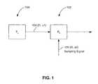
- FIG. 1is a block diagram of a simple communication system.
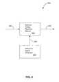
- FIG. 2is a block diagram of a portion of an exemplary receiver.
- FIG. 3is a block diagram of a timing recovery module/system.
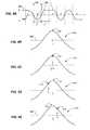
- FIG. 4Ais an illustration of an example analog serial data signal waveform.
- FIG. 4Bis an illustration of an example symbol of the serial data signal of FIG. 4A .
- FIGS. 4C , 4 D, and 4 Eare illustrations of three different data sampling time scenarios.
- FIG. 5Ais a sampled waveform corresponding to the waveform of FIG. 4A .
- FIGS. 5B and 5Care example illustrations of data and phase sample time lines.
- FIGS. 6A , 6 B, and 6 Care illustrations of three different sampling time scenarios.
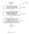
- FIG. 7is a flow diagram of an example method of recovering timing information from a serial data signal.
- FIG. 7Ais a flow chart of an example method expanding on a phase rotating step of the method of FIG. 7 .
- FIG. 8is a block diagram of a phase interpolation environment.
- FIG. 9is a block diagram of a first phase interpolator implementation.
- FIG. 10is a phasor diagram.
- FIG. 11is a schematic of a reference stage circuit that receives a binary control signal.
- FIG. 12is a block diagram of a second phase interpolator implementation.
- FIG. 13is a schematic of a reference stage circuit that receives a control signal having multiple binary subsignals.
- FIGS. 14A and 14Bare each schematics of a phase interpolator including a combining node circuit.
- FIG. 15is a block diagram of a phase interpolator and a phase control signal rotator.
- FIGS. 15A and 15Bare illustrations of alternative implementations of a ring of storage cells used in the phase control signal rotator of FIG. 15 .
- FIGS. 16A-16Care diagrams of phase rings corresponding to the phase interpolator and phase control signal rotator of FIG. 15 .
- FIG. 17is an illustration of a frequency offset in a portion of a timing recovery module.
- FIG. 18is an illustration of compensating for the frequency offset of FIG. 17 in the portion of the timing recovery module.
- FIG. 18Ais a block diagram of a timing recovery system for frequency synchronizing a sampling signal to a serial data signal.
- FIG. 19is a block diagram of a phase error processor of FIG. 18A and FIG. 3 .
- FIG. 20is a flowchart of a method involving phase and frequency tracking.
- FIG. 20Ais a flow chart of an example method expanding on a rotating step of the method of FIG. 20 .
- FIG. 20Bis a block diagram of an example timing recovery system for synchronizing sampling and serial data signal frequencies without using a control signal rotator.
- FIG. 20Cis a flow chart of an example high level method of controlling a phase interpolator, corresponding to the timing recovery systems of FIGS. 18A and 20B .
- FIG. 20Dis a flow chart of an example high level method of frequency synchronizing a sampling signal to a serial data signal.
- FIG. 21is an illustration of an example of a multiple channel communication device constructed on an integrated circuit (IC) chip, according to an embodiment of the present invention.
- ICintegrated circuit
- FIG. 22is an illustration of a receive-lane corresponding to one channel of the multiple channel communication device of FIG. 21 , according to an embodiment of the present invention.
- FIG. 23is an illustration of various example signal waveforms taken from the receive-lane of FIG. 22 .
- FIG. 24is a phase circle representing the phases of sampling signals of FIG. 23 .
- FIG. 25is a block diagram of a data demultiplexer module from FIG. 22 , according to an embodiment of the present invention.
- FIG. 26is a block diagram of an interpolator control module from FIG. 22 , according to embodiment of the present invention.
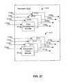
- FIG. 27is a block diagram of a digital data processor of FIGS. 21 and 22 , according to an embodiment of the present invention.
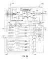
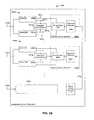
- FIG. 28is a block diagram of a multiple channel communication device, according to an embodiment of the present invention.
- FIG. 29is a flow chart of an example method of processing a serial data signal in multiple data paths of a single channel of a serial data receiver.
- FIG. 30is a flow chart of an example method of frequency synchronizing multiple data sampling signals to multiple corresponding serial data signals.
- FIG. 31is an illustration of an example use of a transceiver/communication device of the present invention in an example signal router.
- FIG. 32is a block diagram of an alternative phase interpolator implementation.
- FIG. 33is a block diagram of another alternative phase interpolator implementation.
- FIG. 1is a block diagram of a simple communication system 100 including a transmitter 100 and a receiver 102 .
- Transmitter 100transmits a serial data signal 104 including, for example, a series of data symbols, to receiver 102 .
- Serial data signal 104has a frequency f 1 (for example, a symbol baud rate f 1 ) and a phase ⁇ 1 both related to a frequency and a phase of an oscillator (not shown) local to transmitter 100 .
- Receiver 102samples serial data signal 104 (for example, symbols included in the serial data signal) to recover data from the serial data signal.
- Receiver 102samples serial data signal at sample times established by a sampling signal 106 generated locally at receiver 102 .
- Locally generated sampling signal 106has a frequency f 2 and a phase ⁇ 2 .
- frequencies f 2 and f 1match one another, and that phases ⁇ 1 and ⁇ 2 are aligned with one another, such that sampling signal 106 causes receiver 102 to sample serial data signal 104 at optimum sample times coinciding with occurrences of a maximum Signal-to-Noise (S/N) level of the serial data signal.
- S/NSignal-to-Noise
- frequency f 2 and phase ⁇ 2are respectively offset from frequency f 1 and phase ⁇ 1 because of differences between the respective oscillators used in transmitter 100 and receiver 102 .
- phase offset between phase ⁇ 1 and phase ⁇ 2can cause receiver 102 to sample serial data signal 104 at sub-optimal sample times, while the frequency offset between frequencies f 1 and f 2 tends to cause the serial data signal to “drift” through sampling signal 106 . Therefore, such offsets can cause errors in recovering the data from serial data signal 104 . Therefore, it is desirable to compensate for such deleterious frequency and phase offsets in receiver 102 in order to optimally recover data from serial data signal 104 .
- FIG. 2is a block diagram of a portion of an exemplary receiver 200 including a timing recovery module 202 of the present invention.
- Receiver 200also includes a reference signal generator 204 .
- Timing recovery module 202receives serial data signal 104 , including, for example, a series of data symbols.
- Reference signal generator 204generates a set of reference signals 206 and provides the reference signal set to timing recovery module 202 .
- timing recovery module 202Based on serial data signal 104 and reference signal set 206 , timing recovery module 202 derives a timing/sampling signal 208 used by receiver 200 to recover data from serial data signal 104 .
- Timing/sampling signal 208is preferably used as a sampling signal in receiver 200 to sample symbols included in serial data signal 104 .
- Timing recovery module 202derives sampling signal 208 such that the sampling signal is phase-aligned with serial data signal 104 and such that the frequency of sampling signal 208 matches the frequency (such as a symbol baud rate) of serial data signal 104 . In this manner, timing recovery module 202 recovers timing information (for example, phase and frequency information) from serial data signal 104 in accordance with the principles of the present invention, as described in detail below.
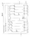
- FIG. 3is a block diagram of timing recovery module 202 according to an embodiment of the present invention.
- Timing recovery module 202includes a phase controller 302 , a phase control signal rotator 304 , and a phase interpolator 306 .
- Phase controller 302includes a data path 308 , a phase path 310 , a phase detector 312 coupled to the data and phase paths, and a phase error processor 314 coupled to the phase detector.
- Reference signal generator 204includes a reference oscillator 330 , a Phase Locked Loop (PLL) 332 , and a signal set generator 334 .
- Reference oscillator 330provides an oscillator signal 335 to PLL 332 .
- PLL 332synthesizes a reference signal 336 based on oscillator signal 335 , and provides the reference signal to signal set generator 334 .
- PLL 332can include an inductance-capacitance (LC), voltage controlled oscillator, for example.
- Signal set generator 334generates the set of reference signals 206 based on reference signal 336 .
- Reference signals included in reference signal set 206all have a same frequency but different predetermined phases.
- Signal set generator 334provides reference signal set 206 to phase interpolator 306 of timing recovery module 202 .
- PLL 332 and signal set generator 334can be implemented as a tapped ring oscillator, for example.
- Phase interpolator 306produces timing/sampling signal 208 (mentioned above in connection with FIG. 2 ) and a second timing/sampling signal 344 offset in phase from sampling signal 208 , based on reference signal set 206 and a plurality of digital phase control signals 340 applied to the phase interpolator.
- Sampling signals 208 and 344each have an interpolated phase controlled in accordance with digital control signals 340 .
- Sampling signal 208 and second sampling signal 344are also referred to herein as data sampling signal 208 and phase sampling signal 344 , for reasons that will become apparent from the description below.
- Data path 308includes sampling and quantizing signal processing modules to sample and quantize serial data signal 104 in accordance with sample times established by sampling signal 208 .
- Data path 308produces a data signal 346 including sampled and quantized data samples representative of serial data signal 104 .
- Data path 308provides data signal 346 to phase detector 312 .
- phase path 310includes sampling and quantizing signal processing modules for sampling and quantizing serial data signal 104 at sample times established by phase sampling signal 344 .
- the sampling times established by phase sampling signal 344are offset in phase from the sample times established by data sampling signal 208 .
- Phase path 310produces a second data signal 348 (referred to herein as a phase signal 348 ) including a series of phase samples also indicative of serial data signal 104 .
- Phase path 310provides phase signal 348 to phase detector 312 . Exemplary data and phase paths are described later in connection with FIGS. 22 and 28 . However, the present invention is not limited to such implementations.
- Phase detector 312detects a phase error 350 between data sampling signal 208 and serial data signal 104 based on the data samples in data signal 346 and the phase samples in phase signal 348 .
- Phase error 350arises because of an undesirable phase offset between data sampling signal 208 (and also phase sampling signal 344 ) and serial data signal 104 .
- phase error 350can be considered a phase error signal indicative of the phase offset between data sampling signal 208 and serial data signal 104 .
- Phase detector 312provides phase error 350 to phase error processor 314 .
- Phase error processor 314process phase error 350 to derive one of a set of rotator control signals or commands 354 .
- Phase error processor 314provides the rotator control command to phase control signal rotator 304 .
- Phase control signal rotator 304stores the digital phase control signals 340 applied to phase interpolator 306 , and manipulates the same in response to the rotator control commands 354 .
- Signal rotator 304rotates the plurality of digital phase control signals 340 and correspondingly the interpolated phase of data sampling signal 208 relative to serial data signal 104 in response to the rotator control commands 354 , such that the sampling signal and the serial data signal become phase aligned with one another.
- FIG. 4Ais an illustration of an example waveform 402 of analog serial data signal 104 .
- Waveform 402represents a Non-Return-to-Zero (NRZ) signal swinging above (i.e., in a positive direction “+”) and below (i.e., in a negative direction “ ⁇ ”) a zero-line 408 , to respectively convey information, such as digital “1s” and “0s.”
- the serial data signal represented by waveform 402includes a series of consecutive symbols 404 each having a symbol period T.
- Dashed vertical lines 406 in FIG. 4Arepresent boundaries between adjacent symbols 404 .
- Received symbols 404have a “rounded” instead of “squared” appearance because of transmission band-limiting effects on serial data signal 104 .
- FIG. 4Bis an illustration of an example symbol 410 from waveform 402 .
- An optimum sample time to at which the receiver can sample symbol 410coincides with a maximum amplitude 412 and correspondingly a maximum symbol S/N of the symbol. In the depicted example, time to coincides with a mid-point of symbol 410 .
- the present inventionadjusts the phase of sampling signal 208 to cause data path 308 to sample each symbol in serial data signal 104 at an optimum data sample time, such as at sample time to depicted in FIG. 4B .
- FIGS. 4C , 4 D, and 4 Eare illustrations of three different data sampling time scenarios.
- FIG. 4Cis an illustration of an on-time data sampling scenario.
- sampling signal 208causes data path 308 to sample data symbol 410 at a sample time t d (represented as an upward pointing arrow in FIG. 4C ) coinciding with optimum sample time t O , to produce an on-time data sample 414 coinciding with mid-point 412 of symbol 410 (depicted in FIG. 4B ). Since sample time t d coincides with optimum sample time to, sampling signal 208 is considered to be phase-aligned with symbol 410 , that is, with serial data signal 104 . In other words, there is a minimum acceptable (or preferably a zero-time) offset between sample time t d and optimum sample time t O .
- FIG. 4Dis an illustration of an early or leading data sampling scenario.
- data sample time t d defined by sampling signal 208precedes (that is, leads) optimum sample time t O because the phase of sampling signal 208 leads the phase of symbol 410 in serial data signal 104 .
- the present inventionretards the phase of sampling signal 208 relative to serial data signal 104 (and thus received symbol 410 ) so as to align sample time t d with optimum sample time t O , as depicted in FIG. 4C .
- FIG. 4Eis an illustration of a late sampling time scenario.
- sample time t dfollows optimum sample time t O because the phase of sampling signal 208 lags the phase of serial data signal 104 (and symbol 410 ).
- the present inventionadvances the phase of sampling signal 208 so as to align sample time t d with optimum sample time t O , as depicted in FIG. 4C .
- FIG. 5Ais a sampled waveform 502 corresponding to serial data signal waveform 402 of FIG. 4A .
- Sampled waveform 502includes a series of spaced data samples 504 (depicted as circles superimposed on the waveform trace) produced by data path 308 in accordance with data sampling signal 208 .
- Sampled waveform 504also includes a series of spaced phase samples 506 (depicted as squares superimposed on the waveform trace) produced by phase path 310 in accordance with phase sampling signal 344 .
- FIG. 5Bis an example data sample timeline 510 established by data sampling signal 208 .
- Data path 308samples serial data signal 104 at data sample times, for example, at sample times t d1 , t d2 , and t d3 (referred to generally as sample time(s) t d ), to produce corresponding data samples 504 1 , 504 2 , and 504 3 included in data signal 346 .
- Data sampling signal 208can be a clock wave having an approximately 50% duty cycle, wherein each sample time t d coincides with a rising edge of the clock wave, for example.
- the clockwavecan have higher or lower duty cycles.
- FIG. 5Cis an example phase sample time line 520 established by phase sampling signal 344 .
- Phase path 310samples serial data signal 104 at phase sample times of, for example, t p1 , t p2 and t p3 (represented as downward pointing arrows and referred to generally as phase sample time(s) t p ), to produce corresponding phase samples 506 1 , 506 2 , and 506 3 included in phase signal 348 .
- Phase sampling signal 344can be a clock wave having an approximately 50% duty cycle, wherein each sample time t p coincides with a rising edge of the clock wave, for example.
- the clockwaveis not limited to a 50% duty cycle.
- FIGS. 6A , 6 B, and 6 Care illustrations of sampling time scenarios corresponding respectively to previously described FIGS. 4C , 4 D and 4 E, except that phase samples are added to FIGS. 6A , 6 B, and 6 C.
- a phase sample 602for example 506 1
- data sample 414for example 504 2
- a phase sample 404for example, 506 2
- First and second phase samples 602 and 604coincide with zero-line 408 in the on-time scenario depicted in FIG. 6A .
- This indicates data sample time t dcoincides with optimum sample time t O , and thus, the phases of sampling signal 208 and serial data signal 104 are optimally aligned with one another.
- leading phase sample 602has a negative value while data sample 414 and trailing phase sample 604 have positive values. This indicates data sample time t d leads optimum sampling time t O , and thus, the phase of sampling signal 208 correspondingly leads the phase of serial data signal 104 .
- leading phase sample 602 and data sample 414have positive values while trailing phase sample 604 has a negative value.
- data sample time t dtrails optimum sample time t O , and thus, the phase of sampling signal 208 correspondingly lags the phase of serial data signal 104 .
- FIG. 7is a flow diagram of an example method 700 of recovering timing information from an NRZ serial data signal (such as serial data signal 104 ) that can be implemented using timing recovery module 202 .
- phase interpolator 306receives the reference signals having different phases in reference signal set 206 .
- Interpolator 306combines in varying relative proportions the reference signals into data sampling signal 208 in response to the plurality of digital phase control signals 340 , thereby producing data sampling signal 208 with a digitally controlled interpolated phase.
- Phase interpolator 306also produces phase sampling signal 344 in response to the digital phase control signal such that the phase sampling signal and the data sampling signal are offset in phase from one another by a predetermined amount corresponding to a fraction (for example, one-half) of a symbol period of serial data signal 104 .
- data path 308samples serial data signal 104 (i.e., the symbols included in serial data signal 104 ) at data sample times t d according to the data sampling signal 208 to produce data samples in data signal 346 .
- Phase path 310also samples serial data signal 104 at phase sample times t p offset in phase relative to the data sample times t d to produce phase samples in phase signal 348 .
- phase detector 312detects a phase error or phase offset between data sampling signal 208 and serial data signal 104 based on the data samples in data signals 346 and the phase samples in phase signal 348 .
- Next steps 708 , 710 and 712 described belowcollectively represent step 706 .
- phase detector 312examines the data samples in data signal 346 to detect occurrences of low-to-high and high-to-low data sample transitions. Such transitions occur at symbol boundaries.
- phase detector 312determines whether each of the data sample times t d near to detected data sample transitions (from step 706 ) is early or late with respect to optimum symbol sample time t O , based on data and phase samples near the detected data sample transitions.
- phase detector 312derives phase error signal 350 indicative of whether each data sample time t d is early or late with respect to the optimum symbol sample time t O .
- Phase detector 312derives as the phase error signal an Early decision signal indicating the phase of sampling signal 208 leads the phase of serial data signal 104 when the data sample time t d precedes optimum sample time t O . Therefore, phase detector 312 produces a series of such Early decision signals over time while the phase of sampling signal 208 leads the phase of serial data signal 104 .
- phase detector 312derives as the phase error signal 350 a Late decision signal indicating the phase of sampling signal 208 lags the phase of serial data signal 104 when the data sample time t d follows optimum sample time t O . Therefore, phase detector 312 produces a series of such Late decision signals over time while the phase of sampling signal 208 lags the phase of serial data signal 104 .
- phase detector 312tends to produce a series of randomly alternating Late and Early decision signals over time while sampling signal 208 and serial data signal 104 are phase aligned with each other.
- phase error processor 314processes the phase error over time (i.e., over many data and phase samples, and corresponding Early/Late decision signals) to determine which of the phase control commands 354 needs to be asserted.
- Phase error processor 314can include an accumulator and/or a filter for accumulating and/or filtering the Early or Late decision signals included in phase error signal 350 , to determined which of the phase control commands 354 needs to be asserted.
- the set of phase control commands 354includes a phase-hold command, a phase-retard command, and a phase-advance command. Phase error processor 314 asserts:
- phase-advance commandwhen the phase of sampling signal 208 lags the phase of serial data signal 104 .
- phase control signal rotator 304rotates the plurality of digital phase control signals 340 , and correspondingly the interpolated phase of data sampling signal 208 , in response to the phase-retard/phase-advance control command asserted by phase error processor 314 , such that data sampling signal 208 and serial data signal 104 become phase aligned with one another as depicted, for example, in FIG. 6A .
- signal rotator 304holds the plurality of digital phase control signals 340 in position, thereby preventing rotation of the phase control signals and correspondingly the interpolated phase of data sampling signal 208 , in response to the phase-hold control command when asserted by phase error processor 314 .
- FIG. 7Ais a flow chart of an example method 770 expanding on phase rotating step 730 of method 700 .
- a step 775is initiated in response to the phase retard command.
- the interpolated phase of sampling signal 208is retarded relative to serial data signal 104 .
- a step 780is initiated in response to the phase advance command.
- the interpolated phase of sampling signal 208is advanced relative to serial data signal 104 .
- a step 785is initiated in response to the phase hold command.
- the interpolated phase of sampling signal 208is held at a present value.
- timing recovery module 202includes a phase interpolator 306 that combines reference signals 206 to generate sampling signals 208 and 344 . These sampling signals are generated by interpolation techniques performed by phase interpolator 306 . These interpolation techniques can provide sampling signal phases that span a complete rotation of 360 degrees. These phases are achieved without the use of conventional techniques, such as time-delays.
- phase interpolation techniques of the present inventionmay be used in other applications.
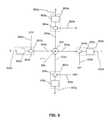
- FIG. 8is a block diagram of a phase interpolation environment 800 .
- Environment 800includes a phase interpolator 801 , such as phase interpolator 306 , and a stage controller 806 , such as phase control signal rotator 304 or other controller.
- the controller 806is not limited to a control signal rotator.
- Interpolator 801includes a plurality of reference stages 802 a - d that are each coupled to stage controller 806 , and a combining node 804 that is coupled to each of reference stages 802 . As shown in FIG. 8 , each reference stage 802 receives a corresponding reference signal 820 . These reference signals are each periodic waveforms that each have a distinct phase. Examples of periodic waveforms include sinusoid, rectangular waveforms, trapezoidal waveforms, and other similar periodic signals.
- each reference stage 802receives a corresponding control signal 822 from stage controller 806 .
- reference stage 802 areceives control signal 822 a
- reference stage 802 breceives control signal 822 b
- reference stage 802 creceives control signal 822 c.
- Each reference stage 802generates a component signal 824 from its corresponding reference signal 822 according to a scaling factor that is the ratio of a component signal 824 magnitude to its corresponding reference signal 820 magnitude.
- a reference stage 802 scaling factoris determined by its corresponding control signal 822 .
- reference stage 802 agenerates component signal 824 a from reference signal 822 a according to a scaling factor determined by control signal 822 a.
- control signals 822may scale as well as activate and deactivate corresponding component signals 824 .
- Component signals 824are each sent to combining node 804 .
- reference stage 802 agenerates a component signal 824 a
- reference stage 802 bgenerates a component signal 824 b
- reference stage 802 cgenerates a component signal 824 c , and so on.
- Combining node 804combines each of component signals 824 to produce an output signal 826 .
- This combiningincludes summing each of the individual component signals 824 (some of which may have a magnitude equal to zero).
- output signal 826is a periodic waveform having a phase that is derived from the phases of component signals 824 . This derivation is referred to herein as phase interpolation.
- Stage controller 806generates stage control signals 822 in response to an interpolation command 828 that is received from a master system controller (not shown), such as rotator control commands 354 received from phase error processor 314 . Exemplary details regarding interpolation command 828 are provided in greater detail below.
- each reference stage 802generates a component signal 824 from a reference signal 820 having a distinct phase.
- These generated component signals 824each have a distinct phase that is determined by the corresponding reference signal 820 phase.
- a component signal 824may have the same or substantially the same phase as its corresponding reference signal 820 .
- a component signal 824may have a phase that is offset by a predetermined phase shift from the corresponding reference signal 820 phase.
- the present inventioncan provide a complete range of phases (i.e., 360 degrees) for output signal 826 .
- This complete rangeis provided through the deployment of more than two reference stages 802 and a strategic predetermined selection of reference signal 820 phases.
- FIG. 9is a block diagram of a first phase interpolator 801 implementation.
- This implementationincludes four reference stages 802 a - d that receive reference signals 820 a - d , respectively.
- Each of reference signals 820 a - dhas a distinct, predetermined phase.
- reference signal 820 ahas a phase 910 a of zero degrees
- reference signal 820 bhas a phase 910 b of 90 degrees
- reference signal 820 chas a phase 910 c of 180 degrees
- reference signal 820 dhas a phase 910 d of 270 degrees.
- the implementation of FIG. 9includes four reference signals 820 having phases 910 that are separated at intervals of 90 degrees.
- each reference stage 802includes a scaling module 902 , and a conversion module 904 that is coupled to scaling module 902 .
- Each conversion module 904receives and converts a reference signal 820 into a corresponding component signal 824 according to a scaling factor.
- Scaling module 902establishes this scaling factor in response to its corresponding control signal 822 . Details regarding implementations of scaling module 902 and conversion module 904 are provided below.
- phase interpolator 801 implementation shown in FIG. 9receives binary control signals 822 that are capable of having two distinct values (i.e., 0 and 1). Accordingly, FIG. 9 shows phase interpolator 801 having an operational state where control signals 822 a , 822 c , and 822 d have values of 0, and control signal 822 d has a value of 1.
- FIG. 10is a phasor diagram that illustrates the phase interpolation capabilities of the phase interpolator 801 implementation shown in FIG. 9 .
- This implementationis capable of generating output signal 826 having one of eight possible phases. These eight possible phases are spaced at intervals of 45 degrees, and span a complete rotation of 360 degrees.
- Phasor diagram 1000includes phasors 1002 , 1006 , 1010 , and 1014 . These phasors have the same phases as reference signal phases 910 a , 910 b , 910 c , and 910 d . respectively.
- phasor diagram 1000includes phasors 1004 , 1008 , 1012 , and 1016 . These phasors have phases that are between reference phases 910 a - d . As shown in FIG. 10 , phasor 1004 has a phase of 45 degrees, phasor 1008 has a phase of 135 degrees, phasor 1012 has a phase of 225 degrees, and phasor 1016 has a phase of 315 degrees. These “between” phases are established through combining two component signals 824 at combining node 804 .
- Table 1shows how the values of control signals 822 a through 822 d determine which of the phasors in FIG. 3 represents output signal 826 .
- phase interpolator 801 implementation of FIG. 9can adjust the phase of output signal 826 among eight distinct phases.
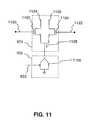
- FIG. 11is an exemplary schematic of a reference stage 802 circuit that receives a binary control signal 822 .
- this circuitmay be employed in the phase interpolator 801 implementation of FIG. 9 .
- reference signals 820 and component signals 824are each differential signal pairs that have an in-phase signal and a 180 degrees out-of-phase signal. Except for a 180 degrees pahse shift, these signals are the same.
- reference signal 820includes an in-phase signal 1120 and an out-of-phase signal 1122 .
- component signal 824includes an in-phase signal 1124 and an out-of-phase signal 1126 . These signals are time varying voltage signals.
- reference stage 802includes a scaling module 902 and a conversion module 904 .
- conversion module 904includes two N channel metal oxide semiconductor (NMOS) field effect transistors (FETs) 1102 and 1104 that each have drain, source, and gate terminals.
- NMOSN channel metal oxide semiconductor
- FETsfield effect transistors
- conversion module 904may employ other transconductance devices.
- Scaling module 902includes a current digital to analog converter (IDAC) 1106 that is coupled to the source terminals of FETs 1102 and 1104 .
- IDACcurrent digital to analog converter
- Scaling module 902receives binary control signal 822 .
- binary control signal 822has a value of 1.
- IDAC 1106operates as a current generator that enables a current 1128 to flow through the drain and source terminals of FETs 1102 and 1104 .
- binary control signal 822has a value of 0.
- IDAC 1106does not enable current 1128 to flow (i.e., current 1128 has zero magnitude).
- the flow of current 1128enables reference signal 820 to be converted into corresponding component signal 824 . That is, source current 1128 enables the conversion of differential reference signals 1120 and 1122 into differential component signals 1124 and 1126 , respectively. This conversion is performed according to a specific scaling factor.
- Differential component signals 1124 and 1126are electrical current signals that are combined at combining node 804 with differential component signals from other reference stages 802 . This combining generates output signal 826 .
- An exemplary combining node 804 circuit schematicis described below with reference to FIG. 14 .
- phase interpolator 801 implementation of FIG. 9is capable of producing eight different phases for control signal 826 at a granularity of 45 degrees.
- the present inventionmay achieve finer phase granularity through implementations where each control signal 822 is capable of having more than two distinct values.
- FIG. 12is a block diagram showing an implementation of phase interpolator 801 that receives control signals 822 capable of having more than two distinct values. This implementation enables output signal 826 to have a greater number of phases than the implementation of FIG. 9 .
- the FIG. 12 implementation of phase interpolator 801includes a plurality of reference stages 802 ′.
- each reference stage 802 ′receives a composite control signal 822 ′ that includes a plurality of binary subsignals 1220 .
- reference stage 802 a ′receives composite control signal 822 a ′, which includes subsignals 1220 a - d .
- These subsignals 1220each contribute to the value of the corresponding composite control signal 822 ′.
- subsignals 1220 a - dcontribute to the value of composite control signal 822 a′.
- Reference stage 802 a ′For purposes of convenience, only reference stage 802 a ′ will be described in detail. However, the other reference stages 802 ′ shown in FIG. 12 may include identical or similar features.
- Reference stage 802 a ′includes a plurality of scaling modules 902 . In particular, the implementation of FIG. 12 shows four scaling modules 902 a - 902 d . However, any number may be employed.
- reference stage 802 a ′includes a conversion module 904 that is coupled to each of scaling modules 902 a - d.
- Scaling modules 902 a - deach receive a respective one of subsignals 1220 a - d . As shown in FIG. 12 , scaling module 902 a receives subsignal 1220 a , scaling module 902 b receives subsignal 1220 b , scaling module 902 c receives subsignal 1220 c , and scaling module 902 d receives subsignal 1220 d.
- Each of scaling modules 902 a - dprovide an individual contribution to the reference stage 802 ′ scaling factor. These individual contributions are based on the value of the corresponding control subsignal 1220 .
- scaling factoris the ratio of a component signal 824 magnitude to its corresponding reference signal 820 magnitude. Accordingly, the aggregate sum of control signals 1220 a - d (also referred to herein as the value of composite control signal 822 ′) determines the reference stage 802 a ′ scaling factor according to a predetermined relationship. According to one such relationship, the reference stage 802 a ′ scaling factor increases with the value of composite control signal 822 ′.
- subsignals 1220 a - dare each binary signals
- aggregate control signals 822 ′can have five distinct values.
- reference stage 802 a ′can generate component signal 824 a from reference signal 820 a according to five different scaling factors.
- One of these scaling factorsmay be equal to zero, thereby causing corresponding component signal 824 a to also have a magnitude of zero.
- the phase interpolator 801 implementation of FIG. 11generates component signals 824 a - d that each may have one of five different magnitudes.
- FIG. 13is a schematic of a reference stage 802 ′ circuit that receives a control signal having multiple binary subsignals.
- this circuitmay be employed in the phase interpolator 801 implementation of FIG. 12 , which receives a plurality of control subsignals 1220 a - d .
- reference signals 820 and component signals 824are each differential signal pairs that have an in-phase signal and a 180 degrees out-of-phase signal. Except for a 180 degrees phase shift, these signals are the same.
- reference signal 820includes an in-phase signal 1320 and an out-of-phase signal 1322 .
- component signal 824includes an in-phase signal 1324 and an out-of-phase signal 1326 .
- These signalsare time varying voltage signals.
- reference stage 802includes a plurality of scaling modules 902 a - d and a conversion module 904 .
- Conversion modules 904includes two N channel metal oxide semiconductor (NMOS) field effect transistors (FETs) 1302 and 1304 that each have drain, source, and gate terminals.
- NMOSN channel metal oxide semiconductor
- FETsfield effect transistors
- conversion modules 904may employ other transconductance devices.
- Scaling modules 902 a - deach include an IDAC 1306 , shown in FIG. 13 as IDACs 1306 a - d .
- IDACs 1306 a - dare each coupled to the source terminals of FETs 1302 and 1304 .
- Each of IDACs 1306 a - dreceives a respective one of binary control subsignals 1220 a - d and, enables a corresponding current 1328 to flow from the source terminals of FETs 1302 and 1304 when the respective control subsignal 1220 has a value of 1.
- IDAC 1306 aenables a current 1328 a to flow when subsignal 1220 a equals 1 .
- the corresponding IDAC 1306does not enable corresponding current 1328 to flow (i.e., corresponding current 1328 has zero magnitude).
- Component signals 1324 and 1326are electrical current signals. These current signals are combined at combining node 804 with component signals from other reference stages 802 . This combining generates output signal 826 .
- An exemplary combining node 804 circuit schematicis described below with reference to FIGS. 14A and 14B .
- FIGS. 14A and 14Bare schematics illustrating a combining node 804 circuit coupled to various reference stage 802 implementations.
- FIG. 14Aillustrates this combining node 804 coupled to the four reference stage 802 circuit of FIG. 11 .
- FIG. 14Billustrates this combining node 804 circuit coupled to four reference stage 802 ′ circuits of FIG. 13 .
- the combining node 804 circuit of FIGS. 14A and 14Bincludes a first resistor 1402 , and a second resistor 1404 .
- Resistors 1402 and 1404are each coupled to a voltage node 1406 , such as a Vdd rail.
- resistors 1402 and 1404are coupled to reference stages 820 a - d .
- resistor 1402is coupled to a FET 1102 within each reference stage 820 .
- resistor 1404is coupled to a FET 1104 within each reference stage 120 .
- the combining node 804 circuit of FIGS. 14A and 14Balso includes a first output node 1408 and a second output node 1410 .
- Output nodes 1408 and 1410provide output signal 826 in the form of a differential signal having an in-phase output signal 1420 and an out-of-phase output signal 1422 .
- Output signals 1420 and 1422are voltage signals measured in relation to a reference voltage, such as ground.
- each reference stage 802includes a conversion module 904 that can generate a corresponding component signal 824 in the form of electrical current signals.
- Examples of such electrical current signalsinclude signals 1124 and 1126 , and signals 1324 and 1326 .
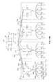
- FIG. 15is a block diagram of phase interpolator 306 and phase control signal rotator 304 according to an embodiment of the present invention.
- the embodiment of phase interpolator 306 depicted in FIG. 15corresponds to the phase interpolator described in connection with FIGS. 12 and 14B .
- the embodiment of control signal rotator 304 depicted in FIG. 15is compatible with the depicted phase interpolator embodiment.
- Other embodiments of phase interpolator 306 (and correspondingly, of control signal rotator 304 )are possible, as would be apparent to one of ordinary skill in the relevant art(s) after reading the description provided herein.
- phase interpolator 306can be implemented in accordance with the phase interpolator embodiments described above in connection with FIGS. 9 , 11 , and 14 A, and below in connection with FIGS. 32 and 33 .
- Phase control signal rotator 304receives phase control command set 354 from phase error processor 314 .
- phase control command set 354includes a phase-advance command 354 a , a phase-retard command 354 b , and a phase-hold command 354 c .
- Phase-advance command 354 acan be considered as a rotate-left command (that is, as a command to rotate the phase of sampling signal 208 in a counter-clockwise direction to advance its phase).
- Phase-retard command 354 acan be considered as a rotate-right command (that is, as a command to rotate the phase of sampling signal 208 in a clockwise direction to retard its phase).
- Signal rotator 304manipulates the digital phase control signals 340 in accordance with an asserted one of phase control commands 354 , and provides the so manipulated digital phase control signals 340 to phase interpolator 306 , as will be described in further detail below.
- Signal rotator 304includes a plurality of storage cells 1502 arranged in a ring configuration, generally referred to as a ring of storage cells 1504 .
- the ring of storage cells 1504includes a plurality of ring segments 1506 a , 1506 b , 1506 c , and 1506 d connected to one another by signal lines 1508 a - 1508 d in the ring configuration, as depicted in FIG. 15 .
- Each of the ring segmentsincludes a plurality of the individual storage cells 1502 .
- Each of the storage cells 1502stores a corresponding one of the plurality of digital phase control signals 340 .
- the ring of storage cells 1504is implemented as a circular shift register responsive to a shift-left, a shift-right, and a shift-enable control input (corresponding to commands 354 a , 354 b , and 354 c , for example).
- Each one of the digital phase control signals 340can be a digital (i.e., logical) “1” or a digital “0,” for example. Therefore, each of the storage cells 1504 can store a digital “1” or a digital “0,” representing one of the digital phase control signals at any given time.
- An exemplary arrangement of digital phase control signals stored in ring 1504is depicted in FIG. 15 , wherein each of the storage cells 1502 included in ring segment 1506 a is a logical “1,” while the remainder of the digital phase control phase signals stored in the storage cells of the other ring segments 1506 b - 1506 d are all logical “0s.”
- digital phase control signals 340are divided among a plurality of digital phase control signal sets 340 a , 340 b , 340 c , and 340 d .
- Each of the signal sets 340 a - 340 dcorresponds to a respective one of ring segments 1506 a , 1506 b , 1506 c , and 1506 d .
- the storage cells included in ring segment 1506 acollectively provide digital phase control signal set 340 a to phase interpolator 306 , and so on.
- phase interpolator 306is capable of bringing about phase shifts having granularity that is finer than 45 degrees.
- phase interpolator 306includes reference stages 802 a ′, 802 b′ , 802 c′ , and 802 d′ , as described above with reference to FIGS. 12 , 13 , and 14 B.
- Each of the reference stages 802 a ′- 802 d ′receives a corresponding one of the set of digital phase control signals 340 a - 340 d (for example, ring segment 1506 a of ring 1504 provides digital phase control signal set 340 a to reference stage 802 a ′, and so on).
- These phase control signal setsare discrete signals capable of having more than two distinct values.
- Control signals sets 340correspond to control signals 822 ′ in FIG. 12 .
- Phase interpolator 306also receives reference signal set 206 ( 820 in FIG.12 ) from reference signal generator 216 (see FIG. 3 ).
- Reference signal set 206includes reference signals 206 a , 206 b , 206 c , and 206 d .
- Reference signals 206 a , 206 b , 206 c and 206 deach have respective relative reference phases of 0°, 90°, 180°, and 270°, for example.
- Reference stages 802 a ′- 80 d ′respectively derive component signals 824 a - 824 d , each having a phase based on (for example, equal to) a corresponding one of the reference signals 206 a - 206 d .
- each of reference stages 802 a ′- 802 d ′scales an amplitude of a corresponding one of reference signals 206 a - 206 d in response to the corresponding one of signal sets 340 a - 340 d , to produce a corresponding one of the component signals 824 a - 824 d , in the manner described previously.
- Combining node 804combines the component signals 802 a ′- 802 d ′ (representing scaled versions of respective reference signals 206 a - 206 d ) into output signal 826 , which is sampling signal 208 in this context.
- phase interpolator 306can be considered as combining the signals in reference signal set 206 , having the different phases, into sampling signal 208 having the interpolated phase.
- Phase interpolator 306varies the relative proportions of the reference signals so combined in response to the plurality of digital phase control signal 340 applied to the interpolator. More specifically, each of signal sets 340 a - 340 d controls the relative proportion of the corresponding one of the reference signals 206 a - 206 d combined into sampling signal 208 by interpolator 306 .
- “relative proportion”refers to a proportion value ranging between a minimum value (such as zero, whereby a reference signal does not contribute to the interpolated phase) and a maximum value.
- phase error processor 314asserts rotate-left command 354 a (that is, the phase-advance command)
- signal rotator ring 1504concurrently shifts-left (that is, in the direction indicated by an arrow L) each one of the digital phase control signals 340 from a present storage element to an adjacent next storage element to the left of the present storage element, in response to the command. Therefore, ring 1504 rotates all of the digital phase control signals 340 in counter-clockwise direction L.
- phase interpolator 306correspondingly rotates the interpolated phase of sampling signal 208 in the counter-clockwise direction (in a direction of decreasing phase), thereby advancing the phase of sampling signal 208 relative to serial data signal 104 .
- phase error processor 314asserts rotate-right command 354 b (that is, the phase-retard command)
- ring 1504concurrently shifts-right (that is, in a clockwise direction indicated by an arrow R) each one of the digital phase control signals 340 from the present storage element to an adjacent next storage element to the right of the present storage element, in response to the command.
- phase interpolator 306correspondingly rotates the interpolated phase of sampling signal 208 in the clockwise direction (in a direction of increasing phase), thereby retarding the phase of sampling signal 208 relative to serial data signal 104 .
- Phase-hold command 354 coverrides either of commands 354 a and 354 b . Therefore, when phase error processor 314 asserts phase-hold command 354 c , ring 1504 holds all of the digital control signals in each present storage element, in response to the command. In other words, phase-hold command 354 c prevents all of the digital phase control signals and correspondingly the interpolated phase of sampling signal 208 from rotating.
- Phase-advance and -retard commands 354 a and 354 bcan be implemented as pulsed commands.
- a single, pulsed phase-advance command 354 a(also referred to as a phase-advance pulse 354 a ) causes an incremental shift-left of one position, and correspondingly, an incremental phase advance, as described above.
- a single, pulsed phase-retard command 354 bcauses an incremental shift-right of one position, and correspondingly, an incremental phase retardation, as is also described above.
- the interpolated phase of sampling signal 208can be incrementally rotated clockwise or counter-clockwise through a range of 3600 by successively pulsing phase-retard and phase-advance commands 354 b and 354 a , respectively.
- the rate at which the interpolated phase of sampling signal 208 rotatescorresponds to the repetition rate of pulsed phase-retard and phase-advance commands 354 b and 354 a.
- FIGS. 15A and 15Bare illustrations of alternative implementations of ring 1504 .
- FIG. 15Ais a block diagram of ring 1504 implemented as a circular shift register 1550 .
- Shift register 1550includes linearly arranged storage cells 1502 linked together to collectively form the ring configuration.
- Shift register 1550includes left and right end cells (not labeled), and a signal line 1530 coupling the end cells together.
- FIG. 15Bis a block diagram of ring 1504 implemented as an array of storage cells 1560 .
- Array 1560includes storage cells 1502 arranged as a matrix of rows and columns, as depicted in FIG. 15B .
- Alternative implementations of ring 1504are possible, as would be apparent to one of ordinary skill in the relevant art after reading the description provided herein.
- FIG. 16Ais an illustration of an exemplary phase ring 1600 useful for describing phase rotation in the present invention.
- Phase ring 1600includes phase segments 1606 a , 1606 b , 1606 c , and 1606 d corresponding to ring segments 1506 a - 1506 d of ring 1504 , and to interpolator stages 802 a ′- 802 b′ , depicted in FIG. 15 .
- Each of the phase segments 1606 a - 1606 dis divided into individual, contiguous phase cells 1608 , each representative of a discrete phase value.
- phase cells 1608 of each of phase segments 1606 a , 1606 b , 1606 c , and 1606 dstraddle respective phase values of 0°, 90°, 180°, and 270° (corresponding to the phases of reference signals 206 a - 206 d ) superimposed around phase ring 1600 .
- the distribution of digital phase control signals (logical “1s” and “0s”) depicted within phase cells 1608corresponds to the exemplary distribution of the same control signals stored in ring 1504 of signal rotator 304 , depicted in FIG. 15 .
- the distribution of digital phase control signals within phase cells 1608 illustrated in FIG. 16Aindicates the relative proportion of the reference phases 0°, 90°, 180°, and 270° included in a resultant phasor 1620 representing the resultant phase of interpolated sampling signal 208 .
- a set of four contiguous logical “1s” 1610resides in phase segment 1606 a , while logical “0s” reside elsewhere. Therefore, reference or component phase 0° is turned full-on, while all of the other phases are turned-off. That is, the relative proportions of the reference phases are such that phase 0° is at a maximum value in sampling signal 208 , while the other phases are at minimum values (of zero, for example). Therefore, the phase of sampling signal 208 output by interpolator 306 is 0°.
- FIG. 16Bis an illustration of phase ring 1600 after signal rotator 304 shifts phase control signals 340 from the positions depicted in FIG. 15 (and correspondingly, in FIG. 16A ) two positions to the right (that is, clockwise) in response to two consecutive phase-retard pulses (i.e., commands) 354 b .
- the consecutive phase-retard pulses 354 bare represented as consecutive clockwise pointing arrows 354 b in FIG. 16B .
- each of component phases 0° and 90°is at half of its maximum value (since the four logical “1s” 1610 are distributed such that two are within phase segment 1606 a corresponding to phase 0° while the other two are within phase segment 1606 b corresponding to phase 90°), while all other phases are turned off. Therefore, interpolator 314 produces sampling signal 208 with an interpolated phase 1620 of 45° (half-way between 0° and 90°).
- FIG. 16Cis an illustration of phase ring 1600 after signal rotator 304 shifts phase control signals 340 from the positions depicted in FIG. 15 (and correspondingly, in FIG. 16A ) two positions to the left (that is, counter-clockwise) in response to two consecutive phase-advance pulses (i.e., commands) 354 a .
- the consecutive phase-advance pulses 354 aare represented as consecutive counter-clockwise pointing arrows 354 a in FIG. 16C .
- each of component phases 0° and 270°is at half of its maximum value (since the four logical “1s” 1610 are distributed such that two are within phase segment 1606 a while the other two are within phase segment 1606 d ), while all other phases are turned off. Therefore, interpolator 314 produces sampling signal 208 with an interpolated phase 1620 of 315° (half-way between 0° and 360°).
- phase interpolator 314can produce sixteen different phases ranging from 0° to 270° with a phase resolution of approximately 22° (360°/16 ⁇ 22°).
- phase control signal logical “1s” within the phase ringremains constant as the digital phase control signals 340 and correspondingly the interpolated phase is rotated.
- sampling signal 208advantageously maintains a constant amplitude as the phase of the sampling signal varies over a range of 360°.
- a constant density of logical “1s”maintains a constant number of currents 1328 . This, in turn, provides constant amplitude output signals 826 .
- FIG. 17is an illustration of a portion of timing recovery module 202 corresponding to when an undesirable angular frequency offset ⁇ exists between serial data signal 104 and sampling signal 208 .
- serial data signal 104has an angular frequency ⁇ d established by a transmit oscillator (not shown) remote from and independent of reference signal generator 304 in the present invention.
- timing recovery module 202 of the present inventionadjusts sampling frequency ⁇ s to compensate for the above mentioned frequency offset ⁇ , to thereby match the frequency of sampling signal 208 to that of serial data signal 104 .
- the present inventionadjusts sampling frequency ⁇ s in the manner described below.
- the present inventioncan rotate phase ⁇ I of sampling signal 208 at different rates to correspondingly produce different sampling frequencies ⁇ s .
- FIG. 18is an illustration of a portion of timing recovery module 202 , wherein phase rotation as described above is used to compensate for a frequency difference between serial data signal 104 and reference signals 206 (that is, phase rotation is used to match the frequency of sampling signal 208 to that of serial data signal 104 ).
- FIG. 18Ais a block diagram of a timing recover system 1810 for frequency synchronizing sampling/timing signal 208 with serial data signal 104 , according to an embodiment of the present invention.
- FIG. 18Ais similar to FIG. 3 .
- Timing recover system 1810includes phase interpolator 306 coupled to a controller 1820 for controlling the phase interpolator.
- Controller 1820includes data and phase paths 308 and 310 , phase detector 312 , phase error processor 314 , and phase control signal rotator 304 .
- Controller 1820applies control signals 340 to phase interpolator 306 to control the interpolated phase of sampling signal 208 (and 344 ).
- Controller 1820includes phase error processor 314 to derive an estimate of a frequency effort between sampling signal 208 and serial data signal 104 , as will be described in further detail below. Controller 1820 manipulates control signals 340 in response to the frequency offset, to cause phase interpolator 306 to rotate the interpolated phase of sampling signal 208 at a rate corresponding the frequency offset, so as to reduce the frequency offset between serial data signal 104 and sampling signal 208 .
- FIG. 19is a block diagram of phase error processor 314 according to an embodiment of the present invention.
- Phase error processor 314includes a short-term phase error processor 1904 , a frequency offset estimator 1906 (also referred to as a long-term phase processor 1906 ), and a rotate command generator 1908 .
- Short-term processor 1904 and frequency offset estimator 1906receive phase error 350 from phase detector 312 .
- Short-term processor 1904integrates phase errors over a relatively short time period, and thus responds relatively rapidly to changes in phase between sampling signal 208 and serial data signal 104 .
- Processor 1904derives a phase adjust signal 1910 in response to the aforementioned short-term phase changes.
- Processor 1904provides the phase adjust signal 1910 to rotate command generator 1908 .
- frequency estimator 1906integrates phase errors over a relatively long period of time (for example, in comparison to short-term processor 1904 ), and thus, responds relatively slowly to changes in phase between sampling signal 208 and serial data signal 104 .
- Frequency estimator 1906examines changes in phase error signal 350 over time t O derive an estimate of a frequency offset, for example, ⁇ , between serial data signal 104 and sampling signal 208 (which may result from a corresponding frequency offset between serial data signal 104 and reference signals 206 ).
- Frequency estimator 1906provides a signal 1912 indicative of frequency offset estimate ⁇ to rotate command generator 1908 .
- frequency estimator 1906 and short-term processor 1904can be combined into a single logic block.
- frequency estimator 1906can integrate signal 1910 output by short-term processor 1904 , to produce signal 1912 .
- short-term processor 1904 and frequency estimator 1906can be implemented as accumulators, such that signals 1910 and 1912 include accumulator over- and under-flow conditions.
- phase error processor 314are possible as would be apparent to one of ordinary skill in the relevant art(s), after reading the description provided herein.
- Rotate command generator 1908derives rotate commands 354 (described above) based on phase adjust signal 1910 and frequency offset estimate signal 1912 .
- Rotate command generator 1908can be part of one or both of blocks 1904 and 1906 .
- rotate command generator 1908generates pulsed phase-advance and phase-retard commands 354 a and 354 b (described above) in response to signals 1910 and 1912 .
- rotate command generator 1908generates pulsed commands 354 at a repetition rate based on the frequency offset estimate ⁇ provided in signal 1912 . This causes digital control signals 340 and correspondingly the phase of sampling signal 208 to rotate at a rate based on (for example, equal to) the frequency offset ⁇ .
- phase adjust signal 1910tends to perturbate the above mentioned repetition rate and correspondingly the phase rotation rate of sampling signal 208 , in response to short-term phase errors.
- timing recovery module 202can adjust sampling signal frequency ⁇ s to match serial data frequency ⁇ d .
- rotate command generator 1908is possible as would be apparent to one of ordinary skill in the relevant art(s), after reading the description provided herein.
- Timing recovery module 202implements a phase and frequency locked (that is, tracking) loop, including phase controller 302 , phase control signal rotator 304 , and phase interpolator 306 , all described previously.
- the phase and frequency locked loopcauses the sampling signal phase and frequency to track the serial data signal phase and frequency, whereby sampling signal 208 and serial data signal 104 remain phase-aligned and frequency synchronized over time.
- Short-term phase error processor (for example, short-term filter) 1904 in phase error processor 314establishes a phase tracking bandwidth of the phase and frequency locked loop.
- Long-term phase processor (for example, filter) 1906establishes a frequency tracking bandwidth of the phase and frequency locked loop.
- Short-term filter 1904responds more quickly to phase changes in serial data signal 104 than does long-term filter 1906 .
- short-term absences of serial data signal 104can cause the phase and frequency locked loop to loose track of the serial data signal phase, since short-term filter 1904 is responsive to such short-term signal losses. Therefore, after such signal losses, the phase and frequency locked loop must re-acquire the serial data signal phase so as to re-establish a phase locked condition.
- phase and frequency locked loopbegins rotating the sampling signal phase at an initial rate to frequency synchronize the sampling and serial data signals 208 and 104 , the phase and frequency locked loop tends to continue rotating the sampling signal phase at the same initial rate during the short-term signal losses. Therefore, when serial data signal 104 returns after such a signal loss, sampling signal 208 tends to still be frequency synchronized with serial data signal 104 (assuming the serial data signal frequency does not change substantially during the signal loss).
- the phase and frequency locked loopneed only re-establish the phase locked condition mentioned above, since the loop is still frequency synchronized with serial data signal 104 . This advantageously reduces the time required to re-acquire the phase locked condition.
- FIG. 20is a flow chart of an example method 2000 of tracking the frequency of serial data signal 104 using phase rotation according to the present invention.
- Step 2000expands on steps 720 and 730 of method 700 described above in connection with FIG. 7 .
- Step 720includes steps 2002 , 2004 , and 2006 .
- short-term phase error processor 2002derives short-term phase adjust signal 1910 by, for example, short-term filtering phase error signal 350 .
- frequency estimator 1906estimates the frequency offset ⁇ between sampling signal 208 and serial data signal 104 .
- Frequency estimator 1906derives the frequency offset estimate by, for example, long-term filtering of phase error 350 .
- rotate command generator 1908generates phase rotate commands (for example, commands 354 a and/or 354 b ) to compensate for both the short-term phase offset and the frequency offset ⁇ .
- Next step 730includes a step 2010 .
- phase control signal rotator 304rotates digital phase control signals 340 and correspondingly interpolated phase ⁇ I of sampling signal 208 in response to phase rotate commands (such as commands 354 a and 354 b ), such that sampling signal 208 and serial data signal 104 become phase aligned and frequency synchronized with one another.
- frequency synchronizedmeans sampling frequency ⁇ s and serial data signal frequency ⁇ d are matched to one another, such that data sample times t d established by the frequency of sampling signal 208 , and coinciding with optimum symbol sample times t O , do not “drift” relative to the symbol sample times t O , over time.
- sampling frequency ⁇ s and serial data signal frequency ⁇ dneed to be related to one another, but not necessarily equal to one another, such that the frequencies are synchronized.
- sampling signal phase ⁇ Iis rotated in the clockwise direction (that is, in the direction of increasing phase) at the necessary rate.
- phase ⁇ Iis rotated in the counter-clockwise direction (that is, in the direction of decreasing phase) at the necessary rate (for example, at a rate equal to the frequency offset ⁇ ).
- the present inventionrotates phasor or phase value 1620 in the clockwise direction around phase ring 1600 to decrease frequency ⁇ s by an amount equal to the rate of rotation.
- the present inventionrotates phasor or phase value 1620 in the counter-clockwise direction around phase ring 1600 to increase frequency ⁇ s by an amount equal to the rate of rotation.
- FIG. 20Ais a flow chart of an example method 2015 expanding on rotating step 2010 of method 2000 .
- a step 2020is initiated when the frequency ⁇ s of sampling signal 208 is greater than the frequency ⁇ d of serial data signal 104 (i.e., when ⁇ s > ⁇ d ) whereby step 2020 decreases the frequency of the sampling signal, and correspondingly, reduces frequency offset ⁇ .
- a step 2025is initiated when the frequency of sampling signal 208 is less than the frequency of serial data signal 104 (i.e., when ⁇ s ⁇ d ), whereby step 2025 increases the frequency of the sampling signal, and correspondingly, reduces frequency offset ⁇ .
- Example timing recovery systems 202 and 1810include control signal rotator 304 for rotating phase control signals 340 , and correspondingly, the interpolated phase of sampling signals 208 and 344 .
- FIG. 20Bis a block diagram of an example timing recovery system 1845 for synchronizing sampling and serial data signal frequencies, without using a control signal rotator.
- timing recovery system 1845includes a phase interpolator 306 ′ and a controller 1850 .
- Phase interpolator 306 ′can be any known phase interpolator capable of adjusting the interpolated phase of sampling signal 208 in response to an interpolator control signal 340 ′ (which may be a signal set 340 ) compatible with the phase interpolator.
- control signal set 340 ′may include multiplexer select signals, and so on.
- Timing recovery system 1845also includes phase detector 312 coupled to a phase error processor 314 ′.
- Phase error processor 314 ′includes a frequency estimator to derive a frequency estimate (that is, a frequency measurement) of the frequency offset between sampling signal 208 and serial data signal 206 , as described above, for example.
- phase detector 312 and phase error processor 314 ′are combined into a single logic block for detecting the frequency offset.
- Phase error processor 314 ′provides control signal 340 ′, indicative of the frequency offset, to phase interpolator 306 ′.
- phase interpolator 306 ′rotates the interpolated phase of sampling signal 208 to reduce the frequency offset between the sampling signal and serial data signal 104 .
- FIG. 20Cis a flow chart of a high level example method 2000 ′ of frequency synchronizing and phase-aligning sampling signal 208 to serial data signal 104 .
- Method 2000 ′is similar to method 2000 , and can be implemented by either of timing control systems 202 and 1845 .
- Method 2000 ′includes a step 720 ′ similar to step 720 of method 2000 .
- step 720 ′includes a generalized sub-step 2006 ′.
- controller 1820 / 1850(of timing system 202 / 1845 ) manipulates phase control signals 340 / 340 ′, applied to phase interpolator 306 / 306 ′, in response to the detected phase and frequency offsets, so as to control the interpolated phase of sampling signal 208 .
- controller 1820rotates phase control signals 340 using rotator 304 (rotating control signals 340 was previously described as part of step 730 / 2010 in FIG. 20 , but is moved into step 720 ′ of method 2000 ′).
- controller 1850can manipulate phase control signals 340 ′ in other ways, as would be apparent to one of ordinary skill in the art after reading the description provided herein.
- controller 1850can modify the values (for example, logic “1” or “0”) of various ones of the phase control signals in accordance with the phase and frequency offset, instead of rotating the phase control signals, so as to correspondingly rotate the interpolated phase of sampling signal 208 .
- Phase error processor 314 ′can include formatting/generating logic to generate and/or manipulate phase control signals 340 ′ such that the phase control signals are compatible with phase interpolator 306 ′.
- a next step 730 ′is similar to step 730 of method 2000 .
- interpolator 306 / 306 ′rotates the interpolated phase of sampling signal 208 in response to phase control signals 340 / 340 ′.
- Step 730 ′is similar to step 730 to the extent phase interpolator 306 rotates the interpolated phase of sampling signal 208 in response to phase control signals 340 .
- step 730 ′does not include rotating phase control signals 340 , since this step is subsumed by previous step 720 ′ in method 2000 ′, as described above.
- FIG. 20Dis a flow chart of a high level example method 2060 of frequency synchronizing sampling signal 208 to serial data signal 104 .
- An initial step 2064includes deriving sampling signal 208 having an interpolated phase (using phase interpolator 306 / 306 ′, for example).
- a next step 2070includes estimating a frequency offset between sampling signal 208 and serial data signal 104 (using phase error processor 314 / 314 ′, for example).
- a next step 2075includes rotating the interpolated phase of sampling signal 208 at a rate corresponding to the frequency offset, so as to reduce the frequency offset.
- FIG. 21is an illustration of an example multiple channel communication device 2100 constructed on an integrated circuit (IC) chip 2102 , according to an embodiment of the present invention.
- Communication device 2100is a multiple channel (that is, multi-channel) transceiver, including multiple receivers and multiple transmitters, as described below. Each of the serial data signals is associated with a different channel.
- Communication device 2100receives multiple analog serial data signals 2104 a , 2104 b , 2104 c , and 2104 d (collectively referred to as multiple serial data signals 2104 ).
- Communication device 2100includes multiple receive-lanes 2106 a , 2106 b , 2106 c , and 2106 d (collectively referred to as multiple receive-lanes 2106 , and each being associated with a receiver/receive-channel of communication device 2100 ).
- Each of receive-lanes 2106receives a corresponding one of multiple serial data signals 2104 , as depicted in FIG. 21 .
- Each of receive-lanes 2106processes the corresponding one of serial data signals 2104 to produce a corresponding one of multiple digital data streams 2108 a , 2108 b , 2108 c , and 2108 d (collectively referred to as digital data streams 2108 ).
- Receive-lanes 2106provide data streams 2108 to a digital data sample processor 2112 .
- Communication device 2100is referred to as a multiple receiver or multi-channel communication device because of the multiple receive-lanes 2106 and associated circuits, described below.
- Communication device 2100includes a master timing generator 2114 for generating a master timing signal 2116 .
- Master timing generator 2114can include a reference oscillator and a PLL, such as reference oscillator 330 and PLL 332 , described above in connection with FIG. 3 .
- Master timing generator 2114provides master timing signal 2116 to each of the multiple receive-lanes 2106 .
- master timing signal 2116includes a pair of differential (that is, complementary) clock signals/waves routed to each of receive-lanes 2106 over a pair of clock lines.
- Communication device 2100also includes multiple transmit-lanes 2130 a , 2130 b , 2130 c , and 2130 d (collectively referred to as multiple transmit-lanes 2130 ).
- Data sample processor 2112provides multiple transmit data streams 2134 a , 2134 b , 2134 c , and 2134 d (collectively referred to as multiple transmit digital data streams 2134 ) to corresponding ones of transmit-lanes 2130 , as depicted in FIG. 21 .
- Master timing generator 2114provides master timing signal 2116 to each of the multiple transmit-lanes 2130 .
- Transmit-lanes 2130each transmit a corresponding one of multiple analog serial data signals 2140 a , 2140 b , 2140 c , and 2140 d (collectively referred to as multiple transmit analog serial data signals 2140 ).
- communication device 2100may include more or fewer receive-lanes 2106 and transmit-lanes 2130 .
- Communication device 2100can include more or less than four receiver and/or transmit lanes in other embodiments.
- FIG. 22is an illustration of receive-lane 2106 a , according to a multiple data path per receive-lane embodiment of the present invention.
- exemplary receive-lane 2106 ais substantially identical to the other receive-lanes 2106 b - d , therefore the following description of receive-lane 2106 a shall suffice for the others.
- Receive-lane 2106 aincludes a data module 2204 , a phase module 2206 , and a sampling signal generator 2208 .
- digital data sample processor 2112includes a data demultiplexer module 2210 a and an interpolator control module 2212 a , both corresponding to receive-lane 2106 a .
- Processor 2112provides interpolator phase control signals 2214 a , including a first phase control signal set 2214 a 1 and a second phase control signal set 2214 a 2 , to sampling signal generator 2208 .
- Sampling signal generator 2208derives a plurality of timing signals required to operate receive-lane 2106 a from master timing signal 2116 , as described below.
- An advantage of deriving such timing signals locally within receive-lane 2106 ais to reduce signal/clock cross-talk and interference across IC chip 2102 , and to reduce the number of signal traces or tracks distributed across the IC chip.
- Sampling signal generator 2208includes a first signal set generator 2220 .
- First signal set generator 2220derives a set of reference signals 2222 having different predetermined phases from master timing signal 2116 .
- Signal set 2222can be the same as or similar to reference signal set 206 described above in connection with FIG. 15 , for example.
- Signal set generator 2220provides signal set 2222 to a phase interpolator module 2224 .
- Phase interpolator module 2224receives signal set 2222 and phase control signals 2214 a from processor 2220 .
- phase interpolator module 2224includes first and second phase interpolators 2226 1 and 2226 2 .
- Each of phase interpolators 2226 1 and 2226 2receives signal set 2222 , together with a respective one of phase control signal sets 2214 a 2 , and 2214 a 2 included in phase control signals 2214 a .
- phase interpolators 2226 1 and 2226 2respectively derive interpolated timing signals 2230 1 and 2230 2 (collectively referred to as interpolated timing signals 2230 ).
- Phase interpolator module 2224provides interpolated timing signals 2230 to a second signal set generator 2234 .
- Second signal set generator 2234derives multiple time-staggered data and phase sampling signals 2238 from interpolated timing signals 2230 . Therefore, time-staggered data and phase sampling signals 2238 each has an interpolated phase corresponding to the interpolated phase of timing signals 2230 .
- Time-staggered data and phase sampling signals 2238include time-staggered data sampling signals d 0 , d 1 , d 2 , and d 3 , and time-staggered phase sampling signals x 0 , x 1 , x 2 , and x 3 .
- Signal set generator 2234generates the multiple time-staggered data and sampling signals 2238 such that data sampling signal d 0 and phase sampling signal x 0 are paired with one another, data sampling signal d 1 and phase sampling signal x 1 are paired with one another, and so on.
- master timing signal 2116has a frequency equal to the symbol frequency B (that is, baud rate B) of serial data signal 2104 a .
- First signal set generator 2220includes four-phase clock generator divide-by-two divider circuits, such that generator 2220 generates four signals in signal set 2222 , each at a frequency B/ 2 .
- phase interpolators 2226 1 and 2226 2produce respective interpolated timing signals 2230 1 and 2230 2 each at a corresponding frequency of B/ 2 .
- timing signals 2230 1 , and 2230 2have respective phases offset from each other by 90 °.
- Second signal set generator 2234includes eight-phase clock generator divide-by-two divider circuits, to produce each of the eight data and sampling signals 2238 at a frequency B/ 4 .
- Data module 2204includes multiple parallel data paths 2242 0 , 2242 1 , 2242 2 , and 2242 3 (collectively referred to as data paths 2242 ). Each of the data paths 2242 0 , 2242 1 , 2242 2 , and 2242 3 receives serial data signal 2104 a .
- Each of data paths 2242 0 , 2242 1 , 2242 2 , and 2242 3samples serial data signal 2104 a according to a corresponding one of time-staggered data sampling signals d 0 , d 1 , d 2 , and d 3 , thereby producing corresponding multiple time-staggered data sample streams 2244 0 , 2244 1 , 2244 2 , and 2244 3 (collectively referred to as multiple time-staggered data sample streams 2244 ), as depicted in FIG. 22 . Therefore, multiple data paths 2242 provide multiple data streams 2244 to processor 2112 .
- serial data signal 22facilitates processing of high frequency serial data signals, such as a serial data signal having a multi-gigabit symbol rate, because each of the parallel data paths can sample the serial data signal at a rate below the multi-gigabit symbol rate, as will be further described below.
- Phase module 2206includes multiple phase paths 2250 0 , 2250 1 , 2250 2 , and 2250 3 (collectively referred to as multiple phase paths 2250 ). Each of the phase paths in multiple phase paths 2250 samples serial data signal 2104 a according to a corresponding one of time-staggered phase sampling signals x 0 , x 1 , x 2 , and x 3 , as depicted in FIG. 22 , thereby producing multiple time-staggered phase sample streams 2252 0 , 2252 1 , 2252 2 , and 2252 3 (collectively referred to as phase sample streams 2252 ). Data streams 2244 and phase streams 2252 collectively form data stream 2108 a depicted in FIG. 21 .
- receive-lane 2106 acan include more or fewer data and phase paths 2242 and 2250 . Also, different ones of receive-lanes 2106 can have different numbers of data paths and different numbers of phase paths. Also, sampling signal generator 2208 in each receive-lane can derive more or less time-staggered data and phase sampling signals according to the number of parallel data and phase paths in the receive-lane. Sampling signal generator 2208 can include less or more phase interpolators, as the need arises to generate more or less timing and sampling signals in the receive-lane.
- each of data paths 2242 and phase paths 2250are substantially identical, and therefore, the following description of exemplary data path 2242 0 shall suffice for the other data and phase paths in such an embodiment.
- Data path 2242 0includes a sampler 2260 , an equalizer 2262 following sampler 2260 , and a quantizer 2264 following the equalizer.
- Sampler 2260samples analog serial data signal 2104 a at sample times established by data sampling signal d 0 , to produce a sampled analog data signal 2270 representative of serial data signal 2104 a .
- Equalizer 2262equalizes sampled analog data signal 2270 to produce an equalized, sampled analog data signal 2272 .
- equalizer 2262reduces inter-symbol interference present in serial data signal 2104 a .
- Quantizer 2264quantizes analog samples of sampled analog signal 2272 into corresponding, quantized digital data samples. Quantizer 2264 provides signal 2244 0 , including the quantized digital data samples, to processor 2112 . Exemplary further details of data and phase paths including equalizers are provided in U.S. Non-Provisional Application No. 9/844,243, filed Apr. 30, 2001. entitled “Methods and Systems for Adaptive Receiver Equalization,” incorporated herein by reference in its entirety.
- Data demultiplexer module 2210 areceives multiple time-staggered (that is, time-skewed) data streams 2244 .
- Data demultiplexer module 2210 atime-deskews and then demultiplexes/deserializes multiple time-staggered data streams 2244 , to produce a demultiplexed data sample stream 2280 a representative of serial data signal 2104 a .
- Demultiplexed data sample stream 2280 aincludes quantized digital data samples arranged in a parallel word format. Therefore, data demultiplexer module 2210 a can be considered a deserializer or serial-tO-parallel converter module.
- Interpolator control module 2212 areceives multiple data streams 2244 from data module 2204 and multiple phase streams 2252 from phase module 2206 . Interpolator control module 2212 a detects phase and frequency offsets between multiple time-staggered data sampling signals d 0 -d 3 and serial data signal 2104 a . Interpolator control module 2212 a derives interpolator phase control signals 2214 a in response to the detected phase and frequency offsets, as described above. In response to phase control signals 2214 , phase interpolator module 2224 rotates the interpolated phase of timing signals 2230 , and correspondingly of time-staggered data and phase sampling signals 2238 , to compensate for the detected phase offset and at a rate corresponding to the detected frequency offset, as described above. In this manner, interpolator control module 2212 a causes time-staggered data sampling signals d 0 -d 3 to be phase-aligned and frequency-synchronized with serial data signal 2104 a.
- FIG. 23is an illustration of various example signal waveforms (b)-(j) from receive-lane 2106 a depicted in FIG. 22 .
- Waveform (b)represents serial data signal 2104 a . including consecutive NRZ symbols 2304 , each having a symbol period T.
- Waveforms (c)-(j)respectively represent time-staggered data and phase sampling signals d 0 , x 0 , d 1 , x 1 , d 2 , x 2 , d 3 , and x 3 .
- each sampling signalfor example, d 0
- data sampling signals d 0 -d 3cause data paths 2242 0-3 to collectively sample four consecutive symbols of serial data signal 2104 a . such that each data path samples a different one of the four consecutive symbols.
- FIG. 24is a phase circle 2400 representing the evenly spaced phases of sampling signals d 0 -x 3 depicted in FIG. 23 .
- a phase rotation of 360°corresponds to a sampling signal period of 4 ⁇ T.
- FIG. 25is a block diagram of data demultiplexermodule 2210 a .
- Data demultiplexer module 2210 aincludes a data deskewer 2502 followed by a data demultiplexer/deserialize 2504 .
- Data deskewer 2502receives multiple time-staggered data sample streams 2244 and multiple data sampling signals d 0 -d 3 .
- Data deskewer 2502time-deskews (that is, removes the time offset between) multiple data sample streams 2244 , and presents corresponding deskewed data sample streams 2510 0-3 to demultiplexer 2504 .
- data deskewer 2502receives four time-staggered symbol samples from data sample streams 2244 , collectively.
- Data deskewer 2502time-deskews the four data samples, and presents four corresponding deskewed data samples to demultiplexer 2504 (in multiple deskewed data streams 2510 0-3 ).
- Data demultiplexer 2504deserializes/demultiplexes the deskewed data sample streams 2510 0-3 to produce deserialized/demultiplexed data sample stream 2280 a .
- Demultiplexer 2504includes a set, such as five, four-bit registers 2510 0-4 , for example. During five consecutive data sampling periods, data demultiplexer module 2210 a consecutively transfers five sets of four deskewed data samples from deskewer 2502 (that is, from data sample streams 2510 0-3 ) into corresponding consecutive ones of the five four-bit registers 2512 0-4 . Thus, twenty serialized data samples are transferred to registers 2512 0-4 in demultiplexer 2504 .
- Demultiplexer 2504constructs a twenty-bit wide parallel word including the twenty serialized data samples mentioned above. Demultiplexer 2504 outputs the twenty-bit parallel word representative of the twenty serialized data samples in demultiplexed data sample stream 2280 a . Demultiplexer 2504 can transfer the twenty-bits as two ten-bit parallel words, for example.
- FIG. 26is a block diagram of interpolator control module 2212 a , according to embodiment of the present invention.
- Interpolator control module 2212 areceives the multiple data streams 2244 and the multiple phase streams 2252 .
- Interpolator control module 2212 aincludes phase detector 2212 , phase error processor 2214 , and a phase control signal rotator 2604 .
- Phase control signal rotator 2604includes a first phase control signal rotator 2204 , and a second phase control signal rotator 2204 2 to correspondingly produce first and second phase control signal sets 2214 a 1 and 2214 a 2 of phase controls signals 2214 a .
- Other embodiments of interpolator control module 2212 aare possible, as would be apparent to one of ordinary skill in the relevant art(s).
- the interpolator control moduleis not limited to an embodiment including a control signal rotator.
- receive-lane 2106 aincludes a timing recovery system/module (such as timing recovery module 202 ) associated with the receive-lane, to phase and frequency track serial data signal 2104 a .
- the timing recovery module associated with receive-lane 2106 aadjusts the interpolated phases of time-staggered data sampling signals d 0 -d 3 such that each of the sampling signals d 0 -d 3 causes the corresponding one of data paths 2242 to optimally sample consecutive symbols in serial data signal 2104 a .
- sampling signal d 0causes data path 2242 0 to sample a mid-point of a first symbol of serial data signal 2104 a .
- sampling signal d 1causes data path 2242 1 to sample a mid-point of a next symbol of serial data signal 2104 a , and so on.
- the timing recovery module associated with receive-lane 2106 afrequency synchronizes data sampling signals d 0 -d 3 with serial data signal 2104 a .
- the timing recovery module associated with receive-lane 2106causes the interpolated phases of data sampling signals d 0 -d 3 to rotate at a rate that synchronizes a common frequency, f s , of sampling signals d 0 -d 3 to the symbol baud rate B of serial data signal 2104 a .
- FIG. 27is a block diagram of processor 2112 , according to an embodiment of the present invention.
- Processor 2112includes multiple data demultiplexer modules 2210 a , 2210 b , 2210 c , and 2210 d (collectively referred to as data demultiplexer modules 2210 ), each corresponding to the data sample streams (that is, data streams 2244 ) of one of data streams 2108 a - 2108 d .
- Processor 2112also includes multiple interpolator control modules 2212 a .
- processor 2112includes a data demultiplexer module and an interpolator control module for each receive channel of communication device 2100 .
- each of the receive-laneis associated with a separate timing recovery module (such as timing recovery module 202 ), wherein each timing recovery module operates independently of each other timing module.
- the timing recovery module associated with receive-lane 2106 atracks a phase and a frequency of serial data signal 2104 a
- the timing recovery module associated with receive-lane 2106 bcan track a different phase and a different frequency of serial data signal 2104 b , and so on.
- the interpolated phases of the sampling signals (d 0 -d 3 ) associated with receive-lane 2106 acan be rotated independently of and at a rate different from the interpolated phases of the sampling signals associated with the other receive-lanes 2106 b - c.
- FIG. 28is a block diagram of a communication device 2800 , corresponding to communication device 2100 , according to another embodiment of the present invention. Unlike the communication device embodiment depicted in FIG. 22 , communication device 2800 does not include multiple parallel sampling paths within a receive-lane of the communication device, as will be described below.
- Communication device 2800is constructed on an IC chip 2802 .
- Communication device 2800includes multiple receive-lanes 2804 a - n .
- Receive-lane 2804 aincludes a sampling signal generator 2806 a , a data path 2808 a , and a phase path 2810 a .
- An interpolatorcontrol module 2812 ais included as part of a digital data processor, not shown.
- Sampling signal generator 2806 aincludes signal set generator 2220 (as described in connection with FIG. 22 , for example), and a phase interpolator 2814 .
- Interpolator control module 2812 aincludes phase detector 2212 , phase error processor 2214 , and phase control signal rotator 2204 , as described previously.
- Phase interpolator 2814provides interpolated sampling signals 2815 1 and 2815 2 to respective data and phase paths 2808 a and 2810 a .
- Data path 2808 a and phase path 2810 acan include the same elements as are included in data path 2242 0 , described in connection with FIG. 22 . If this is the case, then data path 2808 a and phase path 2810 a each provide serial, quantized, digital data samples ( 2816 1 and 2816 2 , respectively) to the digital data processor (not shown).
- a data demultiplexer/deserializercan be added to each of data path 2802 a and phase path 2810 a , after quantizer 2264 in each path. Such a data demultiplexer after quantizer 2264 supplies demultiplexed data samples (in parallel word format) to the digital data processor.
- FIG. 29is a flow chart of an example method of processing a serial data signal in multiple parallel data paths, using receive-lane 2106 a depicted in FIG. 22 , for example.
- An initial step 2902includes generating a master timing signal (for example, using master timing generator 2114 ).
- a next step 2904includes generating multiple time-staggered sampling signals (such as signals d 0 -d 3 ) based on the master timing signal.
- a next step 2906includes sampling a received, analog serial data signal (such as serial data signal 2104 a ) in accordance with each of the multiple time-staggered sampling signals (for example, d 0 -d 3 ), thereby producing multiple time-staggered data sample streams (such as data sample streams 2244 ).
- a received, analog serial data signalsuch as serial data signal 2104 a
- each of the multiple time-staggered sampling signalsfor example, d 0 -d 3
- a next step 2908includes time-deskewing the multiple time-staggered data streams (for example, using deskewer 2502 ).
- a next step 2910includes demultiplexing multiple time-deskewed data streams produced in step 2908 (using, for example, demultiplexer 2504 depicted in FIG. 25 ).
- FIG. 30is a flow chart of an example method 3000 of frequency synchronizing multiple data sampling signals (channels) to corresponding ones of multiple serial data signals using communication device 2100 .
- Method 3000can be implemented using the communication device embodiments depicted in both FIGS. 22 and 28 .
- An initial step 3002includes generating a master timing signal (using master timing generator 2114 , for example).
- a next step 3004includes deriving multiple sampling signals (such as a sampling signal d 0 in receive-lane 2106 a , sampling signal d 0 in received-lane 2106 b , and sampling signal d 0 in received-lane 2106 c ) based on the master timing signal (for example, master timing signal 2116 ).
- Each of the multiple sampling signalsis associated with one of multiple serial data signals (for example, sampling signal d 0 in receive-lane 2106 a is associated with serial data signal 2104 a , sampling signal d 0 in receive-lane 2106 b is associated with serial data signal 2104 b , and so on).
- Each of the sampling signalshas an interpolated phase.
- a next step 3006includes sampling and quantizing each of the multiple serial data signals ( 2104 a , 2104 b , and so on) according to the associated one of the sampling signals (for example, sampling signal d 0 in receive-lane 2104 a , and sampling signal d 0 in receive-lane 2104 b , and so on).
- a next step 3008includes rotating the interpolated phase of each sampling signal at a rate corresponding to a frequency offset between the sampling signal and the serial data signal associated with the sampling signal (such as between sampling signal d 0 in receive-lane 2106 a and serial data signal 2104 a ), whereby each sampling signal is frequency synchronized with each associated serial data signal.
- the present inventionis implemented as a signal router.
- a signal routercan be used to route one or more information signals between a plurality of components.
- FIG. 31is an illustration of an example use of a transceiver of the present invention.
- the transceiver of the present inventionis used in an example signal router 3100 , including a front panel 3102 , a back plane 3104 and one or more interfacing circuit boards 3106 .
- Front panel 3102typically includes a plurality of connectors or “jacks,” to which external devices, such as computers, servers, terminals, communications devices, other routers, and the like, can be coupled.
- the router 3100receives and transmits (i.e., routes) signals between the external devices.
- Each interfacing circuit board 3106includes a finite number of connections to the front panel 3102 for receiving and/or transmitting signals from/tO external devices. Additional interfacing circuit boards 3106 can be utilized to accommodate additional external devices.
- the backplane 3104permits the router 3100 to route signals between multiple interfacing circuit boards 3106 . In other words, the backplane 3104 permits the router 3100 to route signals between external devices that are coupled to different interfacing circuit boards 3106 .
- Interfacing circuit boards 3106can include a variety of digital and/or analog components. When multiple interfacing circuit boards 3106 are utilized, two or more of them can be similar and/or dissimilar. The interfacing circuit boards 3106 illustrated in FIG. 31 are provided for illustrative purposes only.
- Interfacing circuit board 3106 Aoptionally includes one or more interface components 3108 that receive and/or buffer one or more signals received from external devices through the front panel 3102 .
- the interface component 3108receives an optical signal 3109 from the front panel 3102 .
- interfacing component 3108includes one or more optical converters that convert the optical signal 3109 to an electrical analog data signal, illustrated here as an analog serial data signal 3112 .
- interfacing component 3108sends and/or receives one or more other analog data signals 3114 A- n to/from other external devices through the front panel 3102 .
- interfacing component 3108sends and/or receives one or more of the signals 3114 A- n to/from somewhere other than the front panel 3102 .
- the serial analog data signal 3112is provided from the interfacing component 3108 to a transceiver 3110 , which can be implemented as one or more of transceivers 2100 ( FIG. 21 ), for example.
- Transceiver 3110permits the router 3100 to both receiver and transmit analog serial data 3112 from and to external devices.
- a receiver portion 3111(including receive-lanes 2106 , master timing generator 2114 , and digital data sample processor 2112 , for example) converts the serial analog data signal 3112 to one or more digital data signals, illustrated here as parallel digital data signals 3116 .
- the parallel digital data signals 3116are optionally provided to a switch fabric 3118 , which can be a programmable switching fabric.
- the optional switching fabric 3118provides any of a variety of functionalities.
- the optional switching fabric 3118outputs parallel digital data signals 3120 to second transceiver 3122 , which can be implemented as one or more of transceivers 2100 ( FIG. 21 ), for example.
- a transmitter portion 3123(including transmit-lanes 2130 and digital data sample processor 2112 , for example) within the transceiver 3122 converts the parallel digital data signals 3120 to serial analog data signals 3124 and transmits them across the back plane 3104 to other interface circuit boards 3106 n . and/or back to interface circuit board 3106 A.
- a receiver portion 3111 within the transceiver 3122receives analog data signals 3124 from the back plane 3104 and converts them to parallel digital data signals 3120 .
- the parallel digital data signals 3120are provided to the switch fabric 3118 , which provides any of a variety of functionalities.
- the switch fabric 3118outputs parallel digital data signals 3116 to a transmitter 3123 within the transceiver 3110 , which converts them to analog data signals for transmission to an external devices, possibly through the interface component 3108 and the front panel 3102 .
- Additional interface circuit boards 3106 noperate in a similar fashion.
- one or more of the interface circuit boards 3106 A- nare configured with more or less than the functionality described above.
- one or more of the interface circuit boards 3106 A- nare configured to receive analog data signals from the front panel 3102 and to provide them to the back plane 3104 , but not to receive analog data signals 3124 from the back plane 3104 .
- one or more of the interface circuit boards 3106 A- nare configured to analog data signals 3124 from the back plane 3104 and provide them to the front panel, but not to receive analog data signals from the front panel 3102 .
- phase interpolator 306that may be implemented in the manner described above with reference to FIGS. 8-14B .
- other implementationsmay be employed for phase interpolators 306 , 306 ′, 2226 , and 2814 .
- Two alternative example implementationsare illustrated in FIGS. 32 and 33 .
- FIG. 32is a block diagram of a phase interpolator implementation 3200 .
- Implementation 3200includes four reference stages 3202 a - d .
- reference stages 3202 a - dreceive reference signals 820 a - d . respectively.
- reference stages 802 a - dalso receive control signals 822 a - d . respectively.
- each reference stage 3202generates a component signal 824 from its corresponding reference signal 820 according to a scaling factor that is the ratio of its component signal 824 magnitude to its corresponding reference signal 820 magnitude.
- This scaling factoris determined by corresponding control signal 822 , through the use of variable gain amplifiers (VGAs) 3204 .
- Each component signal 824is combined (e.g., summed) at combining node 804 to produce output signal 826 , having an interpolated phase.
- each reference stage 3202includes a VGA 3204 that receives a corresponding reference signal 820 and a corresponding control signal 822 .
- reference stage 3202 areceives reference signal 820 a and control signal 822 a .
- Each VGA 3204has a gain that determined by the value of it corresponding control signal 822 according to a predetermined relationship. In one such relationship, gain increases as the control signal 822 increases. In an alternative relationship, gain decreases as the control signal 822 increases.
- each reference stage 3202is determined by the gain of its VGA 3204 . In particular, for example, as the gain increases, so does the corresponding reference stage 3202 scaling factor.
- FIG. 33is a block diagram of a phase interpolator implementation 3300 . Like implementation 3200 , implementation 3300 includes amplifiers. However, implementation 3300 provides adjustable scaling factors through variable resistance.
- implementation 3300includes four reference stages 3302 a - d that each include a constant gain amplifier 3304 that is coupled to a variable resistance 3306 .
- reference stages 3302 a - dreceive reference signals 820 a - d , respectively.
- reference stages 802 a - dalso receive control signals 822 a - d , respectively.
- its amplifier 3304receives the corresponding reference signal 820 and its variable resistance 3306 receives the corresponding control signal 822 .
- Each reference stage 3302generates a component signal 824 from its corresponding reference signal 822 according to a scaling factor that is the ratio of its component signal 824 magnitude to its corresponding reference signal 820 magnitude. This scaling factor is determined by corresponding component signal 822 , through the use of variable resistances 3306 . Each component signal 824 is combined (e.g., summed) at combining node 804 to produce output signal 826 , having the interpolated phase.
- each reference stage 3302is determined by the value of its variable resistance 3306 . As shown in FIG. 33 , each variable resistance 3306 receives a corresponding control signal 822 . The value of each variable resistance 3306 is determined by the value of its corresponding control signal 822 according to a predetermined relationship. In one such relationship, resistance decreases as the control signal 822 increases. Alternatively, resistance increases as the control signal 822 increases.
- each reference stage 3302is determined by the value of its variable resistance 3306 .
- the corresponding reference stage 3202 scaling factordecreases.
- phase interpolators described aboveare responsive to digital phase control signals for controlling the interpolated phase produced by the interpolator.
- phase interpolatorscan be advantageously used in digital timing recovery systems implemented as “all” digital timing recovery systems including all digital control loops. This can advantageously improve reliability in producing and operating such timing recovery systems.
- the present inventioncan also include phase interpolators responsive to analog phase control signals for controlling the interpolated phase.
- the present inventioncan include reference stages (including VGAs, variable resistances, IDACs, and the like) responsive to phase control signals, each having multiple analog levels, to control the magnitudes of corresponding component signals, and thus, the interpolated phase.
- phase interpolators 306 , 306 ′, 2226 1 , 2226 2 , and 2814can be implemented in many ways, as would be apparent to one of ordinary skill in the relevant art(s) after reading the description provided herein.
- phase interpolatorhaving four reference stages.
- present inventionmay include phase interpolators having any number of reference stages.
- the present inventionmay include a three reference stage phase interpolator.
- each reference stagereceives one of three reference signals that are offset in phase by 120 degrees.
- the present inventionmay include a two reference stage phase interpolator, each reference stage receiving one of two reference signals having spaced phases.
Landscapes
- Engineering & Computer Science (AREA)
- Computer Networks & Wireless Communication (AREA)
- Signal Processing (AREA)
- Power Engineering (AREA)
- Synchronisation In Digital Transmission Systems (AREA)
- Dc Digital Transmission (AREA)
- Cable Transmission Systems, Equalization Of Radio And Reduction Of Echo (AREA)
- Communication Control (AREA)
- Complex Calculations (AREA)
- Radar Systems Or Details Thereof (AREA)
- Information Transfer Systems (AREA)
- Filters That Use Time-Delay Elements (AREA)
Abstract
Description
| TABLE 1 | |||||
| Control Signals | Output Signals | ||||
| 2922a | 2922b | 2922c | 2922d | Phase | |||
| 0 | 0 | 0 | 1 | 1002 | 0 | ||
| 0 | 0 | 1 | 1 | 1004 | 45 | ||
| 0 | 0 | 1 | 0 | 1006 | 90 | ||
| 0 | 1 | 1 | 0 | 1008 | 135 | ||
| 0 | 1 | 0 | 0 | 1010 | 180 | ||
| 1 | 1 | 0 | 0 | 1012 | 225 | ||
| 1 | 0 | 0 | 0 | 1014 | 270 | ||
| 1 | 0 | 0 | 1 | 1016 | 315 | ||
ΔωI=dφI/dt,
where dφI/dt represents the rate at which phase φIis rotated.
ωs=ωr±dφI/dt. or equivalently
ωs=ωr±ΔωI.
Claims (21)
Priority Applications (2)
| Application Number | Priority Date | Filing Date | Title |
|---|---|---|---|
| US11/446,144US8433020B2 (en) | 2000-04-28 | 2006-06-05 | High-speed serial data transceiver and related methods |
| US13/768,923US8798219B2 (en) | 2000-04-28 | 2013-02-15 | High-speed serial data transceiver and related methods |
Applications Claiming Priority (3)
| Application Number | Priority Date | Filing Date | Title |
|---|---|---|---|
| US20081300P | 2000-04-28 | 2000-04-28 | |
| US09/844,441US7058150B2 (en) | 2000-04-28 | 2001-04-30 | High-speed serial data transceiver and related methods |
| US11/446,144US8433020B2 (en) | 2000-04-28 | 2006-06-05 | High-speed serial data transceiver and related methods |
Related Parent Applications (1)
| Application Number | Title | Priority Date | Filing Date |
|---|---|---|---|
| US09/844,441ContinuationUS7058150B2 (en) | 2000-04-28 | 2001-04-30 | High-speed serial data transceiver and related methods |
Related Child Applications (1)
| Application Number | Title | Priority Date | Filing Date |
|---|---|---|---|
| US13/768,923ContinuationUS8798219B2 (en) | 2000-04-28 | 2013-02-15 | High-speed serial data transceiver and related methods |
Publications (2)
| Publication Number | Publication Date |
|---|---|
| US20060227917A1 US20060227917A1 (en) | 2006-10-12 |
| US8433020B2true US8433020B2 (en) | 2013-04-30 |
Family
ID=22743312
Family Applications (12)
| Application Number | Title | Priority Date | Filing Date |
|---|---|---|---|
| US09/844,441Expired - LifetimeUS7058150B2 (en) | 2000-04-28 | 2001-04-30 | High-speed serial data transceiver and related methods |
| US09/844,283Expired - Fee RelatedUS7286597B2 (en) | 2000-04-28 | 2001-04-30 | Methods and systems for adaptive receiver equalization |
| US09/844,296Expired - Fee RelatedUS7012983B2 (en) | 2000-04-28 | 2001-04-30 | Timing recovery and phase tracking system and method |
| US09/844,432Expired - LifetimeUS7016449B2 (en) | 2000-04-28 | 2001-04-30 | Timing recovery and frequency tracking system and method |
| US09/844,266Expired - LifetimeUS6509773B2 (en) | 2000-04-28 | 2001-04-30 | Phase interpolator device and method |
| US10/346,210Expired - Fee RelatedUS6791388B2 (en) | 2000-04-28 | 2003-01-17 | Phase interpolator device and method |
| US10/855,392Expired - Fee RelatedUS6995594B2 (en) | 2000-04-28 | 2004-05-28 | Phase interpolator device and method |
| US11/446,144Expired - Fee RelatedUS8433020B2 (en) | 2000-04-28 | 2006-06-05 | High-speed serial data transceiver and related methods |
| US11/976,185Expired - Fee RelatedUS8223828B2 (en) | 2000-04-28 | 2007-10-22 | Methods and systems for adaptive receiver equalization |
| US13/467,531Expired - Fee RelatedUS8472512B2 (en) | 2000-04-28 | 2012-05-09 | Methods and systems for adaptive receiver equalization |
| US13/768,923Expired - Fee RelatedUS8798219B2 (en) | 2000-04-28 | 2013-02-15 | High-speed serial data transceiver and related methods |
| US13/895,891Expired - Fee RelatedUS8824538B2 (en) | 2000-04-28 | 2013-05-16 | Methods and systems for adaptive receiver equalization |
Family Applications Before (7)
| Application Number | Title | Priority Date | Filing Date |
|---|---|---|---|
| US09/844,441Expired - LifetimeUS7058150B2 (en) | 2000-04-28 | 2001-04-30 | High-speed serial data transceiver and related methods |
| US09/844,283Expired - Fee RelatedUS7286597B2 (en) | 2000-04-28 | 2001-04-30 | Methods and systems for adaptive receiver equalization |
| US09/844,296Expired - Fee RelatedUS7012983B2 (en) | 2000-04-28 | 2001-04-30 | Timing recovery and phase tracking system and method |
| US09/844,432Expired - LifetimeUS7016449B2 (en) | 2000-04-28 | 2001-04-30 | Timing recovery and frequency tracking system and method |
| US09/844,266Expired - LifetimeUS6509773B2 (en) | 2000-04-28 | 2001-04-30 | Phase interpolator device and method |
| US10/346,210Expired - Fee RelatedUS6791388B2 (en) | 2000-04-28 | 2003-01-17 | Phase interpolator device and method |
| US10/855,392Expired - Fee RelatedUS6995594B2 (en) | 2000-04-28 | 2004-05-28 | Phase interpolator device and method |
Family Applications After (4)
| Application Number | Title | Priority Date | Filing Date |
|---|---|---|---|
| US11/976,185Expired - Fee RelatedUS8223828B2 (en) | 2000-04-28 | 2007-10-22 | Methods and systems for adaptive receiver equalization |
| US13/467,531Expired - Fee RelatedUS8472512B2 (en) | 2000-04-28 | 2012-05-09 | Methods and systems for adaptive receiver equalization |
| US13/768,923Expired - Fee RelatedUS8798219B2 (en) | 2000-04-28 | 2013-02-15 | High-speed serial data transceiver and related methods |
| US13/895,891Expired - Fee RelatedUS8824538B2 (en) | 2000-04-28 | 2013-05-16 | Methods and systems for adaptive receiver equalization |
Country Status (6)
| Country | Link |
|---|---|
| US (12) | US7058150B2 (en) |
| EP (3) | EP2104232B1 (en) |
| AT (1) | ATE435536T1 (en) |
| AU (2) | AU2001257348A1 (en) |
| DE (1) | DE60139121D1 (en) |
| WO (2) | WO2001084702A2 (en) |
Cited By (7)
| Publication number | Priority date | Publication date | Assignee | Title |
|---|---|---|---|---|
| US8610476B1 (en)* | 2012-09-14 | 2013-12-17 | Altera Corporation | Apparatus and methods for lock detection for semi-digital and fully-digital clock data recovery |
| US8824538B2 (en) | 2000-04-28 | 2014-09-02 | Broadcom Corporation | Methods and systems for adaptive receiver equalization |
| US9059723B1 (en) | 2014-08-22 | 2015-06-16 | Applied Micro Circuits Corporation | Data dependent jitter reduction of switch driver signals in high speed current steering digital-to-analog converters |
| US9735788B2 (en) | 2015-06-17 | 2017-08-15 | Electronics And Telecommunications Research Institute | Phase locked loop for reducing fractional spur noise |
| US9806977B2 (en) | 2015-11-04 | 2017-10-31 | Nxp Usa, Inc. | Multi-rate overlay mode in wireless communication systems |
| US10374785B2 (en)* | 2016-12-27 | 2019-08-06 | Intel Corporation | Clock phase adjustment using clock and data recovery scheme |
| US11165552B2 (en)* | 2020-03-13 | 2021-11-02 | Anritsu Corporation | Clock recovery device, an error rate measurement device, a clock recovery method, and an error rate measurement method |
Families Citing this family (262)
| Publication number | Priority date | Publication date | Assignee | Title |
|---|---|---|---|---|
| US5978379A (en) | 1997-01-23 | 1999-11-02 | Gadzoox Networks, Inc. | Fiber channel learning bridge, learning half bridge, and protocol |
| US7430171B2 (en) | 1998-11-19 | 2008-09-30 | Broadcom Corporation | Fibre channel arbitrated loop bufferless switch circuitry to increase bandwidth without significant increase in cost |
| US6601007B1 (en)* | 2000-06-30 | 2003-07-29 | Lucent Technologies Inc. | Method and system to increase the performance of high-speed backplanes |
| US7245638B2 (en) | 2000-07-21 | 2007-07-17 | Broadcom Corporation | Methods and systems for DSP-based receivers |
| US7564866B2 (en) | 2000-07-21 | 2009-07-21 | Broadcom Corporation | Methods and systems for digitally processing optical data signals |
| US6990163B2 (en)* | 2000-11-21 | 2006-01-24 | Lsi Logic Corporation | Apparatus and method for acquiring phase lock timing recovery in a partial response maximum likelihood (PRML) channel |
| US7490275B2 (en) | 2001-02-02 | 2009-02-10 | Rambus Inc. | Method and apparatus for evaluating and optimizing a signaling system |
| JP3597142B2 (en)* | 2001-04-20 | 2004-12-02 | 日本電気株式会社 | Center phase determination circuit and center phase determination method |
| JP4542286B2 (en)* | 2001-06-06 | 2010-09-08 | 富士通株式会社 | Parallel signal automatic phase adjustment circuit |
| US7257183B2 (en)* | 2001-07-10 | 2007-08-14 | Rambus Inc. | Digital clock recovery circuit |
| US7345988B2 (en)* | 2001-08-17 | 2008-03-18 | Synopsys, Inc. | System and method for providing crosstalk management for high-speed signaling links |
| US6931089B2 (en)* | 2001-08-21 | 2005-08-16 | Intersil Corporation | Phase-locked loop with analog phase rotator |
| US7158567B2 (en) | 2001-09-11 | 2007-01-02 | Vitesse Semiconductor Corporation | Method and apparatus for improved high-speed FEC adaptive equalization |
| US7301997B1 (en)* | 2001-09-11 | 2007-11-27 | Vitesse Semiconductor Corporation | Method and apparatus for improved high-speed adaptive equalization |
| US6999678B2 (en)* | 2001-11-01 | 2006-02-14 | Pts Corporation | Adaptive method for chirping an optical data signal |
| US20030107986A1 (en)* | 2001-12-11 | 2003-06-12 | Sarnoff Corporation | Method and apparatus for demodulating orthogonal frequency division multiplexed signals |
| US7197101B2 (en)* | 2002-01-02 | 2007-03-27 | Intel Corporation | Phase interpolator based clock recovering |
| US7203259B2 (en)* | 2002-01-02 | 2007-04-10 | Intel Corporation | Phase interpolator |
| US20030130751A1 (en)* | 2002-01-09 | 2003-07-10 | Freesystems Pte.,Ltd. | New filter bank for graphics equalizer implementation |
| DE10203596C1 (en)* | 2002-01-30 | 2003-08-14 | Infineon Technologies Ag | Procedure for sampling phase control |
| JP4107847B2 (en)* | 2002-02-01 | 2008-06-25 | 富士通株式会社 | Timing signal generating circuit and receiving circuit |
| EP1335520B1 (en)* | 2002-02-11 | 2018-05-30 | Semiconductor Components Industries, LLC | Multiplex bus system with duty cycle correction |
| US6922109B2 (en) | 2002-04-01 | 2005-07-26 | Broadcom Corporation | Multiple synthesized clocks with fractional PPM control from a single clock source |
| US7379520B2 (en)* | 2002-04-01 | 2008-05-27 | Broadcom Corporation | Low jitter phase rotator |
| US7162002B2 (en) | 2002-03-01 | 2007-01-09 | Broadcom Corporation | Phase-interpolator based PLL frequency synthesizer |
| US7729453B1 (en) | 2002-04-26 | 2010-06-01 | Bing Li | System and method for fast dynamic adjustment of slicing level for burst mode optical receivers |
| US7664401B2 (en)* | 2002-06-25 | 2010-02-16 | Finisar Corporation | Apparatus, system and methods for modifying operating characteristics of optoelectronic devices |
| US7486894B2 (en)* | 2002-06-25 | 2009-02-03 | Finisar Corporation | Transceiver module and integrated circuit with dual eye openers |
| US7561855B2 (en) | 2002-06-25 | 2009-07-14 | Finisar Corporation | Transceiver module and integrated circuit with clock and data recovery clock diplexing |
| US7437079B1 (en) | 2002-06-25 | 2008-10-14 | Finisar Corporation | Automatic selection of data rate for optoelectronic devices |
| US7809275B2 (en) | 2002-06-25 | 2010-10-05 | Finisar Corporation | XFP transceiver with 8.5G CDR bypass |
| US7151813B2 (en) | 2002-07-17 | 2006-12-19 | Intel Corporation | Techniques to reduce transmitted jitter |
| KR100493026B1 (en)* | 2002-09-09 | 2005-06-07 | 삼성전자주식회사 | Robust symbol timing recovery circuit for telephone line modems |
| US7477847B2 (en)* | 2002-09-13 | 2009-01-13 | Finisar Corporation | Optical and electrical channel feedback in optical transceiver module |
| US20040088594A1 (en)* | 2002-10-31 | 2004-05-06 | Canagasaby Karthisha S. | Receiver tracking mechanism for an I/O circuit |
| US20040096004A1 (en)* | 2002-11-15 | 2004-05-20 | Stmicroelectronics, Inc. | Asymmetrical ethernet transceiver for long reach communications |
| US7016715B2 (en)* | 2003-01-13 | 2006-03-21 | Nellcorpuritan Bennett Incorporated | Selection of preset filter parameters based on signal quality |
| US7869553B1 (en) | 2003-01-21 | 2011-01-11 | Altera Corporation | Digital phase locked loop circuitry and methods |
| DE10303917B3 (en)* | 2003-01-31 | 2004-10-07 | Infineon Technologies Ag | Arrangement and method for synchronizing a signal processing device with a received signal |
| US7149269B2 (en)* | 2003-02-27 | 2006-12-12 | International Business Machines Corporation | Receiver for clock and data recovery and method for calibrating sampling phases in a receiver for clock and data recovery |
| US7397848B2 (en) | 2003-04-09 | 2008-07-08 | Rambus Inc. | Partial response receiver |
| US7489757B2 (en)* | 2003-05-01 | 2009-02-10 | Mitsubishi Denki Kabushiki Kaisha | Clock data recovery circuit |
| JP2006525529A (en) | 2003-05-06 | 2006-11-09 | エスアールアイ インターナショナル | System and method for recording piston rod position information in a magnetic layer on a piston rod |
| US7181180B1 (en) | 2003-05-15 | 2007-02-20 | Marvell International Ltd. | Sigma delta modulated phase lock loop with phase interpolation |
| US7336749B2 (en)* | 2004-05-18 | 2008-02-26 | Rambus Inc. | Statistical margin test methods and circuits |
| US7627029B2 (en) | 2003-05-20 | 2009-12-01 | Rambus Inc. | Margin test methods and circuits |
| US7408981B2 (en)* | 2003-05-20 | 2008-08-05 | Rambus Inc. | Methods and circuits for performing margining tests in the presence of a decision feedback equalizer |
| US7590175B2 (en)* | 2003-05-20 | 2009-09-15 | Rambus Inc. | DFE margin test methods and circuits that decouple sample and feedback timing |
| US7636411B2 (en)* | 2003-06-30 | 2009-12-22 | Intel Corporation | I/O link with configurable forwarded and derived clocks |
| US7343443B1 (en)* | 2003-07-08 | 2008-03-11 | Hewlett-Packard Development Company, L.P. | Updated package generation based on analysis of bank dependency |
| US7092408B1 (en)* | 2003-08-12 | 2006-08-15 | Wideband Semiconductors, Inc. | Plesiochronous synchronization of remote subscriber's clock to hub's clock |
| US7196562B1 (en) | 2003-08-26 | 2007-03-27 | Integrated Device Technology, Inc. | Programmable clock drivers that support CRC error checking of configuration data during program restore operations |
| US7151398B2 (en)* | 2003-08-26 | 2006-12-19 | Integrated Device Technology, Inc. | Clock signal generators having programmable full-period clock skew control |
| US6977539B1 (en) | 2003-08-26 | 2005-12-20 | Integrated Device Technology, Inc. | Clock signal generators having programmable full-period clock skew control and methods of generating clock signals having programmable skews |
| US7406118B2 (en)* | 2003-09-11 | 2008-07-29 | Xilinx, Inc. | Programmable logic device including programmable multi-gigabit transceivers |
| US7668271B2 (en)* | 2003-09-30 | 2010-02-23 | Rambus Inc. | Clock-data recovery (“CDR”) circuit, apparatus and method for variable frequency data |
| US7475270B1 (en)* | 2003-11-03 | 2009-01-06 | Hewlett-Packard Development Company, L.P. | System and method for waveform sampling |
| US20050191059A1 (en)* | 2004-01-12 | 2005-09-01 | Clariphy | Use of low-speed components in high-speed optical fiber transceivers |
| US7904895B1 (en) | 2004-04-21 | 2011-03-08 | Hewlett-Packard Develpment Company, L.P. | Firmware update in electronic devices employing update agent in a flash memory card |
| US7639736B2 (en) | 2004-05-21 | 2009-12-29 | Rambus Inc. | Adaptive receive-side equalization |
| US8050373B2 (en)* | 2004-06-28 | 2011-11-01 | Broadcom Corporation | Phase interpolator based transmission clock control |
| US8526940B1 (en) | 2004-08-17 | 2013-09-03 | Palm, Inc. | Centralized rules repository for smart phone customer care |
| KR100823129B1 (en)* | 2004-08-18 | 2008-04-21 | 삼성전자주식회사 | Tracking device and method of mobile communication system |
| SG120185A1 (en) | 2004-08-30 | 2006-03-28 | Micron Technology Inc | Delay lock loop phase glitch error filter |
| US7088191B2 (en)* | 2004-09-29 | 2006-08-08 | Intel Corporation | Delay interpolation in a ring oscillator delay stage |
| US7161443B2 (en) | 2004-09-30 | 2007-01-09 | Broadcom Corporation | Temperature compensated crystal oscillator |
| US7571360B1 (en)* | 2004-10-26 | 2009-08-04 | National Semiconductor Corporation | System and method for providing a clock and data recovery circuit with a fast bit error rate self test capability |
| US20060140320A1 (en)* | 2004-12-23 | 2006-06-29 | Jensen Richard S | Mechanism to adjust a clock signal based on embedded clock information |
| US7817767B2 (en)* | 2004-12-23 | 2010-10-19 | Rambus Inc. | Processor-controlled clock-data recovery |
| US7613237B1 (en)* | 2005-01-13 | 2009-11-03 | Advanced Micro Devices, Inc. | Built-in test feature to facilitate system level stress testing of a high-speed serial link that uses a forwarding clock |
| EP2375662B1 (en) | 2005-01-20 | 2018-09-26 | Rambus Inc. | High-speed signaling systems with adaptable pre-emphasis and equalization |
| US7680226B2 (en)* | 2005-03-24 | 2010-03-16 | Dell Products L.P. | Minimizing dynamic crosstalk-induced jitter timing skew |
| US7259553B2 (en)* | 2005-04-13 | 2007-08-21 | Sri International | System and method of magnetically sensing position of a moving component |
| US20060245485A1 (en)* | 2005-04-28 | 2006-11-02 | Intel Corporation | Continuous-time equalizer |
| US7792232B2 (en)* | 2005-06-30 | 2010-09-07 | Intel Corporation | Method and system for link jitter compensation including a fast data recovery circuit |
| US7196564B2 (en)* | 2005-07-22 | 2007-03-27 | Texas Instruments Incorporated | High frequency balanced phase interpolator |
| KR100633774B1 (en)* | 2005-08-24 | 2006-10-16 | 삼성전자주식회사 | Clock recovery circuit with wide phase margin |
| US7816975B2 (en)* | 2005-09-20 | 2010-10-19 | Hewlett-Packard Development Company, L.P. | Circuit and method for bias voltage generation |
| US7379382B2 (en) | 2005-10-28 | 2008-05-27 | Micron Technology, Inc. | System and method for controlling timing of output signals |
| US7593496B2 (en)* | 2005-12-27 | 2009-09-22 | Intel Corporation | Phase interpolator |
| US7327174B2 (en)* | 2006-03-14 | 2008-02-05 | Intel Corporation | Fast locking mechanism for delay lock loops and phase lock loops |
| US8331512B2 (en) | 2006-04-04 | 2012-12-11 | Rambus Inc. | Phase control block for managing multiple clock domains in systems with frequency offsets |
| US7639737B2 (en) | 2006-04-27 | 2009-12-29 | Rambus Inc. | Adaptive equalization using correlation of edge samples with data patterns |
| US8209676B2 (en) | 2006-06-08 | 2012-06-26 | Hewlett-Packard Development Company, L.P. | Device management in a network |
| US7831004B2 (en)* | 2006-06-13 | 2010-11-09 | Panasonic Corporation | Synchronous detecting circuit |
| JP2008011189A (en)* | 2006-06-29 | 2008-01-17 | Nec Electronics Corp | Time interleave a/d conversion apparatus |
| EP2047420A4 (en) | 2006-07-27 | 2009-11-18 | Hewlett Packard Development Co | User experience and dependency management in a mobile device |
| KR101301698B1 (en)* | 2006-08-24 | 2013-08-30 | 고려대학교 산학협력단 | Linear phase detector and clock & data recovery circuit including thereof |
| US7716514B2 (en)* | 2006-09-19 | 2010-05-11 | International Business Machines Corporation | Dynamic clock phase alignment between independent clock domains |
| US7904741B2 (en)* | 2006-09-19 | 2011-03-08 | International Business Machines Corporation | Dynamic clock phase alignment between independent clock domains |
| US20080069278A1 (en)* | 2006-09-19 | 2008-03-20 | Baumgartner Steven J | Asynchronous Phase Rotator Control |
| US20080075221A1 (en)* | 2006-09-21 | 2008-03-27 | Jia-Long Lai | Apparatus and related method for detecting phase of input data |
| US7782990B1 (en)* | 2006-09-27 | 2010-08-24 | Xilinx, Inc. | Method of and circuit for oversampling a signal in an integrated circuit |
| US8068890B2 (en)* | 2006-09-29 | 2011-11-29 | Nellcor Puritan Bennett Llc | Pulse oximetry sensor switchover |
| KR20090082208A (en) | 2006-10-06 | 2009-07-29 | 램버스 인코포레이티드 | Clock and data recovery using fractional estimates of frequency derivatives |
| US8031763B2 (en)* | 2006-12-28 | 2011-10-04 | Intel Corporation | Automatic tuning circuit for a continuous-time equalizer |
| EP2498464A2 (en) | 2007-01-08 | 2012-09-12 | Rambus Inc. | Adaptive continuous-time line equalizer for correcting the first post-cursor ISI |
| WO2008085299A1 (en) | 2007-01-09 | 2008-07-17 | Rambus Inc. | Receiver with clock recovery circuit and adaptive sample and equalizer timing |
| US7925156B2 (en)* | 2007-01-16 | 2011-04-12 | Broadlight, Ltd. | Apparatus and method for measuring the quality of burst signals and performing optical line diagnostics |
| US7831416B2 (en)* | 2007-07-17 | 2010-11-09 | Caterpillar Inc | Probabilistic modeling system for product design |
| JP2009088793A (en)* | 2007-09-28 | 2009-04-23 | Fujitsu Ltd | Synchronization system, synchronization signal transmission device, clock supply device, and synchronization method |
| US7864912B1 (en)* | 2007-10-19 | 2011-01-04 | Marvell International Ltd. | Circuits, architectures, a system and methods for improved clock data recovery |
| WO2009055103A2 (en) | 2007-10-22 | 2009-04-30 | Rambus, Inc. | Low-power source-synchronous signaling |
| US7495607B1 (en)* | 2007-11-28 | 2009-02-24 | Topcon Gps, Llc | Method and apparatus for adaptive processing of signals received from satellite navigation systems |
| EP2241050B1 (en) | 2008-02-01 | 2018-08-08 | Rambus Inc. | Receiver with enhanced clock and data recovery |
| TWI379201B (en)* | 2008-05-27 | 2012-12-11 | Novatek Microelectronics Corp | Data description method and related packet and testing system for a serial transmission interface |
| WO2010009763A1 (en)* | 2008-07-23 | 2010-01-28 | Nokia Corporation | Bearing determination using signals transformed into frequency domain |
| US8261160B1 (en)* | 2008-07-30 | 2012-09-04 | Lattice Semiconductor Corporation | Synchronization of serial data signals |
| JP5542413B2 (en)* | 2008-11-12 | 2014-07-09 | 東京応化工業株式会社 | Resist composition and resist pattern forming method |
| KR100992000B1 (en)* | 2008-12-11 | 2010-11-04 | 주식회사 하이닉스반도체 | Multiphase Clock Generation Circuit and Control Method Thereof |
| US7809518B2 (en)* | 2008-12-17 | 2010-10-05 | Agilent Technologies, Inc. | Method of calibrating an instrument, a self-calibrating instrument and a system including the instrument |
| KR100973013B1 (en)* | 2008-12-22 | 2010-07-30 | 삼성전기주식회사 | Sampling Frequency Offset Estimation System |
| US8149907B2 (en)* | 2009-01-07 | 2012-04-03 | Mediatek Inc. | Adaptive equalization apparatus with equalization parameter setting adaptively adjusted according to edges of equalizer output monitored in real-time manner and related method thereof |
| US8063683B2 (en) | 2009-06-08 | 2011-11-22 | Integrated Device Technology, Inc. | Low power clock and data recovery phase interpolator |
| CN102460972B (en) | 2009-06-30 | 2015-10-14 | 拉姆伯斯公司 | For adjusting clock signal with the method for comfort noise, system and integrated circuit |
| US8289061B2 (en)* | 2009-09-29 | 2012-10-16 | Integrated Device Technology, Inc. | Technique to reduce clock recovery amplitude modulation in high-speed serial transceiver |
| US8503515B2 (en)* | 2010-01-14 | 2013-08-06 | Integrated Device Technology Inc. | High speed switch with data converter physical ports and processing unit |
| US8503514B2 (en)* | 2010-01-14 | 2013-08-06 | Integrated Device Technology Inc. | High speed switch with data converter physical ports |
| WO2011100412A2 (en)* | 2010-02-11 | 2011-08-18 | Sri International | Displacement measurement system and method using magnetic encodings |
| WO2011139503A1 (en) | 2010-04-30 | 2011-11-10 | Rambus Inc. | Low power edge and data sampling |
| US9288089B2 (en) | 2010-04-30 | 2016-03-15 | Ecole Polytechnique Federale De Lausanne (Epfl) | Orthogonal differential vector signaling |
| US9106238B1 (en) | 2010-12-30 | 2015-08-11 | Kandou Labs, S.A. | Sorting decoder |
| US9246713B2 (en) | 2010-05-20 | 2016-01-26 | Kandou Labs, S.A. | Vector signaling with reduced receiver complexity |
| US9288082B1 (en) | 2010-05-20 | 2016-03-15 | Kandou Labs, S.A. | Circuits for efficient detection of vector signaling codes for chip-to-chip communication using sums of differences |
| US9450744B2 (en) | 2010-05-20 | 2016-09-20 | Kandou Lab, S.A. | Control loop management and vector signaling code communications links |
| US9479369B1 (en) | 2010-05-20 | 2016-10-25 | Kandou Labs, S.A. | Vector signaling codes with high pin-efficiency for chip-to-chip communication and storage |
| US9251873B1 (en) | 2010-05-20 | 2016-02-02 | Kandou Labs, S.A. | Methods and systems for pin-efficient memory controller interface using vector signaling codes for chip-to-chip communications |
| US8593305B1 (en) | 2011-07-05 | 2013-11-26 | Kandou Labs, S.A. | Efficient processing and detection of balanced codes |
| US9596109B2 (en) | 2010-05-20 | 2017-03-14 | Kandou Labs, S.A. | Methods and systems for high bandwidth communications interface |
| US9124557B2 (en) | 2010-05-20 | 2015-09-01 | Kandou Labs, S.A. | Methods and systems for chip-to-chip communication with reduced simultaneous switching noise |
| US9300503B1 (en) | 2010-05-20 | 2016-03-29 | Kandou Labs, S.A. | Methods and systems for skew tolerance in and advanced detectors for vector signaling codes for chip-to-chip communication |
| US9362962B2 (en) | 2010-05-20 | 2016-06-07 | Kandou Labs, S.A. | Methods and systems for energy-efficient communications interface |
| US9059816B1 (en) | 2010-05-20 | 2015-06-16 | Kandou Labs, S.A. | Control loop management and differential delay correction for vector signaling code communications links |
| US9401828B2 (en) | 2010-05-20 | 2016-07-26 | Kandou Labs, S.A. | Methods and systems for low-power and pin-efficient communications with superposition signaling codes |
| US9077386B1 (en) | 2010-05-20 | 2015-07-07 | Kandou Labs, S.A. | Methods and systems for selection of unions of vector signaling codes for power and pin efficient chip-to-chip communication |
| US9985634B2 (en) | 2010-05-20 | 2018-05-29 | Kandou Labs, S.A. | Data-driven voltage regulator |
| US9564994B2 (en) | 2010-05-20 | 2017-02-07 | Kandou Labs, S.A. | Fault tolerant chip-to-chip communication with advanced voltage |
| WO2011151469A1 (en) | 2010-06-04 | 2011-12-08 | Ecole Polytechnique Federale De Lausanne | Error control coding for orthogonal differential vector signaling |
| US8212697B2 (en)* | 2010-06-15 | 2012-07-03 | Csr Technology Inc. | Methods of and arrangements for offset compensation of an analog-to-digital converter |
| JP5522256B2 (en)* | 2010-07-29 | 2014-06-18 | 富士通株式会社 | Signal generation circuit and wireless transmission / reception apparatus having the same |
| KR20120036018A (en)* | 2010-10-07 | 2012-04-17 | 삼성전자주식회사 | Apparatus and method for frequency offset estimation for high speed in wireless communication system |
| US9275720B2 (en) | 2010-12-30 | 2016-03-01 | Kandou Labs, S.A. | Differential vector storage for dynamic random access memory |
| US8665928B1 (en)* | 2011-02-18 | 2014-03-04 | Xilinx, Inc. | Circuit for generating an output clock signal synchronized to an input clock signal |
| TW201315155A (en) | 2011-09-20 | 2013-04-01 | Sunplus Technology Co Ltd | Phase interpolation circuit |
| US8686775B2 (en) | 2011-09-22 | 2014-04-01 | Fujitsu Limited | Piecewise linear phase interpolator |
| US8680939B2 (en) | 2011-10-20 | 2014-03-25 | Lockheed Martin Corporation | Differential equalizer and system, method, and computer program product thereof |
| US8674773B2 (en) | 2012-01-31 | 2014-03-18 | Fujitsu Limited | Phase interpolator with voltage-controlled oscillator injection-lock |
| GB2498937A (en)* | 2012-01-31 | 2013-08-07 | Texas Instruments Ltd | A high data rate SerDes receiver arranged to receive input from a low data rate SerDes transmitter |
| WO2013119209A1 (en) | 2012-02-07 | 2013-08-15 | Intel Corporation | Gated ring oscillator-based digital eye width monitor for high-speed i/o eye width measurement |
| US9130277B2 (en) | 2012-02-27 | 2015-09-08 | Qualcomm Incorporated | RF baseband beamforming |
| US8942299B2 (en)* | 2012-02-27 | 2015-01-27 | Qualcomm Incorporated | Baseband beamforming |
| US9577816B2 (en) | 2012-03-13 | 2017-02-21 | Rambus Inc. | Clock and data recovery having shared clock generator |
| US8836394B2 (en) | 2012-03-26 | 2014-09-16 | Rambus Inc. | Method and apparatus for source-synchronous signaling |
| US9071407B2 (en) | 2012-05-02 | 2015-06-30 | Ramnus Inc. | Receiver clock test circuitry and related methods and apparatuses |
| US9268683B1 (en) | 2012-05-14 | 2016-02-23 | Kandou Labs, S.A. | Storage method and apparatus for random access memory using codeword storage |
| JP5936926B2 (en)* | 2012-06-07 | 2016-06-22 | ルネサスエレクトロニクス株式会社 | Reception circuit, clock recovery circuit, and communication system |
| US8929499B2 (en)* | 2012-09-29 | 2015-01-06 | Intel Corporation | System timing margin improvement of high speed I/O interconnect links by using fine training of phase interpolator |
| FR2996970B1 (en)* | 2012-10-16 | 2015-05-15 | Commissariat Energie Atomique | UWB RECEIVER WITH TEMPORAL DERIVATIVE CORRECTION |
| US9036764B1 (en) | 2012-12-07 | 2015-05-19 | Rambus Inc. | Clock recovery circuit |
| US9397868B1 (en) | 2012-12-11 | 2016-07-19 | Rambus Inc. | Split-path equalizer and related methods, devices and systems |
| US9450590B2 (en)* | 2012-12-13 | 2016-09-20 | Coherent Logix, Incorporated | Clock distribution network for multi-frequency multi-processor systems |
| TWI491235B (en) | 2012-12-26 | 2015-07-01 | Mstar Semiconductor Inc | Timing recovery device and method |
| US9306551B2 (en) | 2013-01-22 | 2016-04-05 | Mediatek Inc. | Interpolator and interpolation cells with non-uniform driving capabilities therein |
| WO2014124450A1 (en) | 2013-02-11 | 2014-08-14 | Kandou Labs, S.A. | Methods and systems for high bandwidth chip-to-chip communications interface |
| US9032274B2 (en)* | 2013-02-14 | 2015-05-12 | Advanced Micro Devices, Inc. | Method and apparatus for clock and data recovery |
| CN110166217B (en) | 2013-04-16 | 2022-05-17 | 康杜实验室公司 | High bandwidth communication interface method and system |
| EP2997704B1 (en) | 2013-06-25 | 2020-12-16 | Kandou Labs S.A. | Vector signaling with reduced receiver complexity |
| WO2015038867A1 (en) | 2013-09-16 | 2015-03-19 | Rambus Inc. | Source-synchronous receiver using edged-detection clock recovery |
| KR102077743B1 (en)* | 2013-09-26 | 2020-04-08 | 삼성전자주식회사 | Adaptive equalizer and control method thereof |
| US9021154B2 (en) | 2013-09-27 | 2015-04-28 | Intel Corporation | Read training a memory controller |
| US8934594B1 (en)* | 2013-10-14 | 2015-01-13 | Xilinx, Inc. | Sampling position tuning |
| US8971447B1 (en)* | 2013-10-17 | 2015-03-03 | Fujitsu Limited | Variable delay of data signals |
| US9544167B2 (en)* | 2013-11-19 | 2017-01-10 | Massachusetts Institute Of Technology | Methods and apparatus for monitoring occupancy of wideband GHz spectrum and sensing and decoding respective frequency components of time-varying signals using sub-nyquist criterion signal sampling |
| US9106465B2 (en) | 2013-11-22 | 2015-08-11 | Kandou Labs, S.A. | Multiwire linear equalizer for vector signaling code receiver |
| TWI543596B (en)* | 2013-12-26 | 2016-07-21 | 晨星半導體股份有限公司 | Multimedia interface receiving circuit |
| CN104811190B (en)* | 2014-01-28 | 2017-12-08 | 晨星半导体股份有限公司 | multimedia interface receiving circuit |
| US9806761B1 (en) | 2014-01-31 | 2017-10-31 | Kandou Labs, S.A. | Methods and systems for reduction of nearest-neighbor crosstalk |
| US9100232B1 (en) | 2014-02-02 | 2015-08-04 | Kandou Labs, S.A. | Method for code evaluation using ISI ratio |
| US9369312B1 (en) | 2014-02-02 | 2016-06-14 | Kandou Labs, S.A. | Low EMI signaling for parallel conductor interfaces |
| KR102240544B1 (en) | 2014-02-28 | 2021-04-19 | 칸도우 랩스 에스에이 | Clock-embedded vector signaling codes |
| TWI519119B (en)* | 2014-04-17 | 2016-01-21 | 創意電子股份有限公司 | Clock data recovery circuit and method |
| US9509437B2 (en) | 2014-05-13 | 2016-11-29 | Kandou Labs, S.A. | Vector signaling code with improved noise margin |
| US9148087B1 (en) | 2014-05-16 | 2015-09-29 | Kandou Labs, S.A. | Symmetric is linear equalization circuit with increased gain |
| JP6203121B2 (en)* | 2014-05-28 | 2017-09-27 | 株式会社東芝 | Signal conversion apparatus and method, signal restoration apparatus and method, and information processing apparatus |
| US9852806B2 (en) | 2014-06-20 | 2017-12-26 | Kandou Labs, S.A. | System for generating a test pattern to detect and isolate stuck faults for an interface using transition coding |
| US9112550B1 (en) | 2014-06-25 | 2015-08-18 | Kandou Labs, SA | Multilevel driver for high speed chip-to-chip communications |
| EP3138253A4 (en) | 2014-07-10 | 2018-01-10 | Kandou Labs S.A. | Vector signaling codes with increased signal to noise characteristics |
| US9432082B2 (en) | 2014-07-17 | 2016-08-30 | Kandou Labs, S.A. | Bus reversable orthogonal differential vector signaling codes |
| KR101943048B1 (en) | 2014-07-21 | 2019-01-28 | 칸도우 랩스 에스에이 | Multidrop data transfer |
| WO2016019384A1 (en) | 2014-08-01 | 2016-02-04 | Kandou Labs, S.A. | Orthogonal differential vector signaling codes with embedded clock |
| US9674014B2 (en) | 2014-10-22 | 2017-06-06 | Kandou Labs, S.A. | Method and apparatus for high speed chip-to-chip communications |
| JP6302092B2 (en)* | 2014-12-18 | 2018-03-28 | 株式会社東芝 | Wireless communication apparatus, integrated circuit, transmission method, reception method, and communication method |
| CN107852153B (en)* | 2015-06-03 | 2021-04-27 | 马维尔亚洲私人有限公司 | Delay locked loop |
| US9397822B1 (en) | 2015-06-11 | 2016-07-19 | Applied Micro Circuits Corporation | Split loop timing recovery |
| KR101978470B1 (en) | 2015-06-26 | 2019-05-14 | 칸도우 랩스 에스에이 | High-speed communication system |
| US9755819B2 (en) | 2015-07-01 | 2017-09-05 | Rambus Inc. | Phase calibration of clock signals |
| US9379880B1 (en)* | 2015-07-09 | 2016-06-28 | Xilinx, Inc. | Clock recovery circuit |
| CN108141798B (en)* | 2015-10-09 | 2022-12-27 | 索尼集团公司 | Measuring device, method of operating a device, network node, method of modifying a frequency band |
| US9557760B1 (en) | 2015-10-28 | 2017-01-31 | Kandou Labs, S.A. | Enhanced phase interpolation circuit |
| US9577815B1 (en) | 2015-10-29 | 2017-02-21 | Kandou Labs, S.A. | Clock data alignment system for vector signaling code communications link |
| US10055372B2 (en) | 2015-11-25 | 2018-08-21 | Kandou Labs, S.A. | Orthogonal differential vector signaling codes with embedded clock |
| US10003315B2 (en) | 2016-01-25 | 2018-06-19 | Kandou Labs S.A. | Voltage sampler driver with enhanced high-frequency gain |
| EP3446403B1 (en) | 2016-04-22 | 2021-01-06 | Kandou Labs S.A. | High performance phase locked loop |
| US10003454B2 (en) | 2016-04-22 | 2018-06-19 | Kandou Labs, S.A. | Sampler with low input kickback |
| US10153591B2 (en) | 2016-04-28 | 2018-12-11 | Kandou Labs, S.A. | Skew-resistant multi-wire channel |
| US10193716B2 (en) | 2016-04-28 | 2019-01-29 | Kandou Labs, S.A. | Clock data recovery with decision feedback equalization |
| EP3449379B1 (en) | 2016-04-28 | 2021-10-06 | Kandou Labs S.A. | Vector signaling codes for densely-routed wire groups |
| US10056903B2 (en) | 2016-04-28 | 2018-08-21 | Kandou Labs, S.A. | Low power multilevel driver |
| US9667407B1 (en) | 2016-05-13 | 2017-05-30 | Credo Technology Group Limited | Integrated multi-channel receiver having independent clock recovery modules with enhanced inductors |
| WO2018010816A1 (en)* | 2016-07-15 | 2018-01-18 | Huawei Technologies Co., Ltd. | High capacity optical data transmission using intensity-modulation and direct-detection |
| CN108701525B (en) | 2016-07-27 | 2020-07-31 | 默升科技集团有限公司 | Enhanced Inductors for Integrated Multichannel Receivers |
| US9906358B1 (en) | 2016-08-31 | 2018-02-27 | Kandou Labs, S.A. | Lock detector for phase lock loop |
| US10411922B2 (en) | 2016-09-16 | 2019-09-10 | Kandou Labs, S.A. | Data-driven phase detector element for phase locked loops |
| US10305495B2 (en)* | 2016-10-06 | 2019-05-28 | Analog Devices, Inc. | Phase control of clock signal based on feedback |
| US10200188B2 (en) | 2016-10-21 | 2019-02-05 | Kandou Labs, S.A. | Quadrature and duty cycle error correction in matrix phase lock loop |
| US10200218B2 (en) | 2016-10-24 | 2019-02-05 | Kandou Labs, S.A. | Multi-stage sampler with increased gain |
| US10372665B2 (en) | 2016-10-24 | 2019-08-06 | Kandou Labs, S.A. | Multiphase data receiver with distributed DFE |
| US9800438B1 (en)* | 2016-10-25 | 2017-10-24 | Xilinx, Inc. | Built-in eye scan for ADC-based receiver |
| US10483910B2 (en) | 2017-02-02 | 2019-11-19 | Credo Technology Group Limited | Multiport inductors for enhanced signal distribution |
| WO2018187899A1 (en) | 2017-04-10 | 2018-10-18 | Credo Technology Group Ltd. | Cage‐shielded interposer inductances |
| CN115333530A (en) | 2017-05-22 | 2022-11-11 | 康杜实验室公司 | Multi-mode data-driven clock recovery method and apparatus |
| US10116468B1 (en) | 2017-06-28 | 2018-10-30 | Kandou Labs, S.A. | Low power chip-to-chip bidirectional communications |
| US10686583B2 (en) | 2017-07-04 | 2020-06-16 | Kandou Labs, S.A. | Method for measuring and correcting multi-wire skew |
| US10203226B1 (en) | 2017-08-11 | 2019-02-12 | Kandou Labs, S.A. | Phase interpolation circuit |
| US10313105B2 (en) | 2017-09-12 | 2019-06-04 | Credo Technology Group Limited | Fractional-N PLL based clock recovery for SerDes |
| TWI672007B (en)* | 2017-09-26 | 2019-09-11 | 北京集創北方科技股份有限公司 | Fast channel detection and compensation circuit and communication device using same |
| US10347283B2 (en) | 2017-11-02 | 2019-07-09 | Kandou Labs, S.A. | Clock data recovery in multilane data receiver |
| US10326623B1 (en) | 2017-12-08 | 2019-06-18 | Kandou Labs, S.A. | Methods and systems for providing multi-stage distributed decision feedback equalization |
| CN109905137B (en)* | 2017-12-11 | 2020-11-24 | 博通集成电路(上海)股份有限公司 | Receiver for determining sampling phase and method for determining sampling phase |
| US10554380B2 (en) | 2018-01-26 | 2020-02-04 | Kandou Labs, S.A. | Dynamically weighted exclusive or gate having weighted output segments for phase detection and phase interpolation |
| KR102478782B1 (en)* | 2018-05-18 | 2022-12-20 | 삼성전자주식회사 | Eye opening measurement circuit calculating difference between sigma levels, receiver including the same, and method for measuring eye opening |
| KR102445856B1 (en) | 2018-06-12 | 2022-09-21 | 칸도우 랩스 에스에이 | Low Latency Combination Clock Data Recovery Logic Circuitry and Charge Pump Circuitry |
| TWI658700B (en)* | 2018-07-16 | 2019-05-01 | 創意電子股份有限公司 | Integrated circuit, multi-channels transmission apparatus and signal transmission method thereof |
| US10778236B2 (en) | 2019-01-04 | 2020-09-15 | Credo Technology Group Limited | PLL with wide frequency coverage |
| CN111669278B (en)* | 2019-03-06 | 2024-11-12 | 马维尔亚洲私人有限公司 | A method and device for waking up the physical layer of a first node in low power mode |
| US10958251B2 (en) | 2019-04-08 | 2021-03-23 | Kandou Labs, S.A. | Multiple adjacent slicewise layout of voltage-controlled oscillator |
| US10673443B1 (en) | 2019-04-08 | 2020-06-02 | Kandou Labs, S.A. | Multi-ring cross-coupled voltage-controlled oscillator |
| US10630272B1 (en) | 2019-04-08 | 2020-04-21 | Kandou Labs, S.A. | Measurement and correction of multiphase clock duty cycle and skew |
| US10720936B1 (en)* | 2019-07-22 | 2020-07-21 | eTopus Technology Inc. | ADC reconfiguration for different data rates |
| WO2021014629A1 (en)* | 2019-07-25 | 2021-01-28 | 日本電信電話株式会社 | Synchronous detection device, synchronous detection method, and program |
| US10972107B2 (en)* | 2019-07-31 | 2021-04-06 | Apple Inc. | Serial data receiver with sampling clock skew compensation |
| RU193622U1 (en)* | 2019-08-16 | 2019-11-07 | ФЕДЕРАЛЬНОЕ ГОСУДАРСТВЕННОЕ КАЗЕННОЕ ВОЕННОЕ ОБРАЗОВАТЕЛЬНОЕ УЧРЕЖДЕНИЕ ВЫСШЕГО ОБРАЗОВАНИЯ Военная академия Ракетных войск стратегического назначения имени Петра Великого МИНИСТЕРСТВА ОБОРОНЫ РОССИЙСКОЙ ФЕДЕРАЦИИ | AGREED FILTER |
| US11038602B1 (en) | 2020-02-05 | 2021-06-15 | Credo Technology Group Limited | On-chip jitter evaluation for SerDes |
| US12207210B2 (en)* | 2020-02-27 | 2025-01-21 | Nippon Telegraph And Telephone Corporation | Receiving method, wireless communication method, receiving station, wireless communication system, and receiving program |
| US11031939B1 (en)* | 2020-03-19 | 2021-06-08 | Mellanox Technologies, Ltd. | Phase detector command propagation between lanes in MCM USR serdes |
| US10992501B1 (en) | 2020-03-31 | 2021-04-27 | Credo Technology Group Limited | Eye monitor for parallelized digital equalizers |
| US10892763B1 (en)* | 2020-05-14 | 2021-01-12 | Credo Technology Group Limited | Second-order clock recovery using three feedback paths |
| RU202508U1 (en)* | 2020-07-07 | 2021-02-20 | ФЕДЕРАЛЬНОЕ ГОСУДАРСТВЕННОЕ КАЗЕННОЕ ВОЕННОЕ ОБРАЗОВАТЕЛЬНОЕ УЧРЕЖДЕНИЕ ВЫСШЕГО ОБРАЗОВАНИЯ Военная академия Ракетных войск стратегического назначения имени Петра Великого МИНИСТЕРСТВА ОБОРОНЫ РОССИЙСКОЙ ФЕДЕРАЦИИ | DEVICE FOR PROCESSING BROADBAND PHASOMANIPULATED SIGNAL |
| KR102711854B1 (en)* | 2020-08-18 | 2024-09-30 | 삼성전자주식회사 | Receiver circuit performing adaptive equalization and system including the same |
| US11115040B1 (en) | 2020-11-02 | 2021-09-07 | eTopus Technology Inc. | ADC slicer reconfiguration for different channel insertion loss |
| US11177986B1 (en)* | 2020-11-24 | 2021-11-16 | Texas Instruments Incorporated | Lane adaptation in high-speed serial links |
| KR102779809B1 (en) | 2021-01-08 | 2025-03-12 | 삼성전자주식회사 | Monotonic and glitch-free phase interpolator and communication device including the same |
| US11115251B1 (en)* | 2021-01-22 | 2021-09-07 | Litrinium, Inc. | PAM4 equalization DSM |
| US11463092B1 (en) | 2021-04-01 | 2022-10-04 | Kanou Labs Sa | Clock and data recovery lock detection circuit for verifying lock condition in presence of imbalanced early to late vote ratios |
| US11563605B2 (en) | 2021-04-07 | 2023-01-24 | Kandou Labs SA | Horizontal centering of sampling point using multiple vertical voltage measurements |
| US11496282B1 (en) | 2021-06-04 | 2022-11-08 | Kandou Labs, S.A. | Horizontal centering of sampling point using vertical vernier |
| US20230223942A1 (en)* | 2022-01-12 | 2023-07-13 | Sean Iwasaki | Circuitry, System(s), and Method(s) to Automatically Align, Tune and Lock CDR Circuitry |
| US12328380B2 (en) | 2022-05-26 | 2025-06-10 | Samsung Display Co., Ltd. | System and method for configuring serial receiver |
| US20240223192A1 (en)* | 2022-12-31 | 2024-07-04 | Advanced Micro Devices, Inc. | Multi-phase clock gating with phase selection |
| US12261928B2 (en) | 2023-07-28 | 2025-03-25 | Credo Technology Group Limited | Receivers and method with fast sampling phase and frequency acquisition |
| US20250158623A1 (en)* | 2023-11-15 | 2025-05-15 | Ciena Corporation | Multiphase clock generator |
| US12401488B1 (en) | 2024-03-28 | 2025-08-26 | Credo Technology Group Limited | Dynamic timing loop gain to compensate phase interpolation nonlinearities |
Citations (123)
| Publication number | Priority date | Publication date | Assignee | Title |
|---|---|---|---|---|
| US3749845A (en) | 1971-08-27 | 1973-07-31 | Bell Telephone Labor Inc | Digital data communication system |
| US4126853A (en) | 1975-11-05 | 1978-11-21 | Rockwell International Corporation | Non-linear digital-to analog conversion |
| US4218756A (en) | 1978-06-19 | 1980-08-19 | Bell Telephone Laboratories, Incorporated | Control circuit for modifying contents of packet switch random access memory |
| US4500954A (en) | 1981-10-15 | 1985-02-19 | International Business Machines Corporation | Cache bypass system with post-block transfer directory examinations for updating cache and/or maintaining bypass |
| US4620180A (en)* | 1985-10-21 | 1986-10-28 | Northern Telecom Limited | Serial-to-parallel converter for high-speed bit streams |
| US4633226A (en) | 1984-12-17 | 1986-12-30 | Black Jr William C | Multiple channel analog-to-digital converters |
| US4763319A (en) | 1986-05-19 | 1988-08-09 | Bell Communications Research, Inc. | Multi-rate synchronous virtual circuit network for voice and data communications |
| US4910713A (en) | 1988-06-27 | 1990-03-20 | Digital Euipment Corporation | High input impedance, strobed CMOS differential sense amplifier |
| US4916717A (en) | 1989-01-23 | 1990-04-10 | Racal Data Communications Inc. | Clock resynchronization mechanism |
| US4918734A (en) | 1986-05-23 | 1990-04-17 | Hitachi, Ltd. | Speech coding system using variable threshold values for noise reduction |
| WO1990007243A1 (en) | 1988-12-16 | 1990-06-28 | Motorola, Inc. | Automatic frequency control in the presence of data |
| US4989074A (en) | 1988-09-27 | 1991-01-29 | Matsushita Electric Industrial Co., Ltd. | Digital automatic gain control apparatus |
| US5022057A (en)* | 1988-03-11 | 1991-06-04 | Hitachi, Ltd. | Bit synchronization circuit |
| US5150380A (en) | 1989-10-18 | 1992-09-22 | Nec Corporation | Receiver capable of removing both intersymbol interference and frequency offset |
| US5235671A (en) | 1990-10-15 | 1993-08-10 | Gte Laboratories Incorporated | Dynamic bit allocation subband excited transform coding method and apparatus |
| US5247541A (en) | 1991-05-30 | 1993-09-21 | Oki Electric Industry Co., Ltd. | Automatic equalizer for a data transmission channel |
| US5272476A (en)* | 1991-04-04 | 1993-12-21 | The United States Of America As Represented By The Secretary Of The Navy | Data acquisition system having novel, low power circuit for time-division-multiplexing sensor array signals |
| US5313501A (en)* | 1992-06-15 | 1994-05-17 | Digital Equipment Corporation | Method and apparatus for deskewing digital data |
| US5394402A (en) | 1993-06-17 | 1995-02-28 | Ascom Timeplex Trading Ag | Hub for segmented virtual local area network with shared media access |
| US5396224A (en) | 1991-11-22 | 1995-03-07 | Hewlett-Packard Company | Telemetered patient location system and method |
| US5414830A (en) | 1990-07-11 | 1995-05-09 | Bull, S.A. | Apparatus for serialization and deserialization of data, and resultant system for digital transmission of serial data |
| EP0483439B1 (en) | 1990-10-30 | 1995-06-28 | International Business Machines Corporation | Self-training adaptive equalization method and apparatus |
| US5467464A (en) | 1993-03-09 | 1995-11-14 | Apple Computer, Inc. | Adaptive clock skew and duty cycle compensation for a serial data bus |
| US5485490A (en) | 1992-05-28 | 1996-01-16 | Rambus, Inc. | Method and circuitry for clock synchronization |
| EP0515074B1 (en) | 1991-05-21 | 1996-03-20 | National Semiconductor Corporation | Frequency controlled oscillator for high frequency phase-locked loop |
| US5526361A (en) | 1992-07-01 | 1996-06-11 | Telefonaktiebolaget Lm Ericsson | Bit demultiplexor for demultiplexing a serial data stream |
| US5550546A (en) | 1993-11-19 | 1996-08-27 | Trw Inc. | Advanced parameter encoder with dual integrated pulse present detection and channel/sector arbitration |
| US5550860A (en) | 1993-11-12 | 1996-08-27 | International Business Machines Corporation | Digital phase alignment and integrated multichannel transceiver employing same |
| US5554945A (en) | 1994-02-15 | 1996-09-10 | Rambus, Inc. | Voltage controlled phase shifter with unlimited range |
| US5561665A (en) | 1994-08-11 | 1996-10-01 | Matsushita Electric Industrial Co., Ltd. | Automatic frequency offset compensation apparatus |
| US5574724A (en) | 1995-05-26 | 1996-11-12 | Lucent Technologies Inc. | Adjustment of call bandwidth during a communication call |
| US5574756A (en) | 1994-05-25 | 1996-11-12 | Samsung Electronics Co., Ltd. | Method for generating digital communication system clock signals & circuitry for performing that method |
| US5579346A (en) | 1994-01-19 | 1996-11-26 | Kabushiki Kaisha Toshiba | Automatic frequency control method and circuit for use in a delay detection type demodulator |
| US5581585A (en) | 1994-10-21 | 1996-12-03 | Level One Communications, Inc. | Phase-locked loop timing recovery circuit |
| US5583859A (en) | 1994-08-30 | 1996-12-10 | Bell Communications Research, Inc. | Data labeling technique for high performance protocol processing |
| US5614855A (en) | 1994-02-15 | 1997-03-25 | Rambus, Inc. | Delay-locked loop |
| US5633899A (en) | 1996-02-02 | 1997-05-27 | Lsi Logic Corporation | Phase locked loop for high speed data capture of a serial data stream |
| US5650954A (en) | 1996-01-30 | 1997-07-22 | Seagate Technology, Inc. | Frequency and time domain adaptive filtration in a sampled communication channel |
| EP0805447A2 (en) | 1996-04-30 | 1997-11-05 | Cirrus Logic, Inc. | Adaptive equalization and interpolated timing recovery in a sampled amplitude read channel for magnetic recording |
| WO1997042731A1 (en) | 1996-05-07 | 1997-11-13 | Silicon Image, Inc. | System and method for high-speed skew-insensitive multi-channel data transmission |
| US5703905A (en) | 1996-02-16 | 1997-12-30 | Globespan Technologies, Inc. | Multi-channel timing recovery system |
| US5742604A (en) | 1996-03-28 | 1998-04-21 | Cisco Systems, Inc. | Interswitch link mechanism for connecting high-performance network switches |
| US5758078A (en) | 1990-02-14 | 1998-05-26 | Fujitsu Limited | Global server for transmitting calling capability to mediator and local servers for requesting calling capability from the mediator to transmit resource capability to global server |
| US5757857A (en) | 1994-07-21 | 1998-05-26 | The Regents Of The University Of California | High speed self-adjusting clock recovery circuit with frequency detection |
| US5757770A (en) | 1994-10-11 | 1998-05-26 | Thomson-Csf | Method and device for the control of congestion in sporadic exchanges of data packets in a digital transmission network |
| US5768268A (en) | 1995-07-19 | 1998-06-16 | Watkins Johnson Company | Wideband base station architecture for digital cellular communications system |
| US5822143A (en) | 1996-06-11 | 1998-10-13 | Western Digital Corporation | Decision feedback equalization implementation of partial-response signaling in a magnetic recording channel |
| US5848109A (en) | 1994-08-04 | 1998-12-08 | Bull S.A. | Apparatus and process for sampling a serial digital signal |
| US5852629A (en) | 1993-12-10 | 1998-12-22 | Fujitsu Limited | Repeater |
| US5870438A (en) | 1996-09-26 | 1999-02-09 | Rockwell Int'l. Corp. | Fast resynchronization system for high-speed data transmission |
| US5881107A (en) | 1996-03-11 | 1999-03-09 | Deutsche Itt Industries, Gmbh | Transmission system for digital signals, and transmitter and receiver therefor |
| US5881108A (en) | 1996-02-22 | 1999-03-09 | Globespan Technologies, Inc. | Adaptive pre-equalizer for use in data communications equipment |
| US5892922A (en) | 1997-02-28 | 1999-04-06 | 3Com Corporation | Virtual local area network memory access system |
| WO1999017452A1 (en) | 1997-09-30 | 1999-04-08 | Trustees Of Princeton University | High-speed serial-to-parallel and analog-to-digital conversion |
| US5931898A (en) | 1997-02-25 | 1999-08-03 | Lucent Technologies Inc | Finite impulse response filter |
| US5945862A (en) | 1997-07-31 | 1999-08-31 | Rambus Incorporated | Circuitry for the delay adjustment of a clock signal |
| US5949820A (en) | 1996-08-01 | 1999-09-07 | Nec Electronics Inc. | Method for optimizing an equalization and receive filter |
| US5953338A (en) | 1996-12-13 | 1999-09-14 | Northern Telecom Limited | Dynamic control processes and systems for asynchronous transfer mode networks |
| GB2336074A (en) | 1998-03-30 | 1999-10-06 | 3Com Technologies Ltd | Phase alignment of data in high speed parallel data buses using a multi-phase low frequency sampling clock |
| GB2336075A (en) | 1998-03-30 | 1999-10-06 | 3Com Technologies Ltd | Phase alignment of data in high speed parallel data buses using adjustable high frequency sampling clocks |
| US5966415A (en) | 1997-06-13 | 1999-10-12 | Cirrus Logic, Inc. | Adaptive equalization in a sub-sampled read channel for a disk storage system |
| US5991339A (en) | 1998-01-16 | 1999-11-23 | Intel Corporation | Adaptive equalization using a minimum- jitter criterion |
| US6002279A (en) | 1997-10-24 | 1999-12-14 | G2 Networks, Inc. | Clock recovery circuit |
| US6005445A (en) | 1996-12-29 | 1999-12-21 | Sony Corporation | Phase adjustment circuit including a ring oscillator in a phase locked loop |
| US6009534A (en) | 1998-06-01 | 1999-12-28 | Texas Instruments Incorporated | Fractional phase interpolation of ring oscillator for high resolution pre-compensation |
| US6016082A (en) | 1998-02-13 | 2000-01-18 | Sun Microsystems, Inc. | Low phase noise LC oscillator for microprocessor clock distribution |
| US6035409A (en) | 1998-05-18 | 2000-03-07 | National Semiconductor Corporation | 1000 mb phase picker clock recovery architecture using interleaved phase detectors |
| US6038269A (en) | 1997-11-20 | 2000-03-14 | National Semiconductor Corporation | Detection for digital communication receivers |
| US6041090A (en) | 1995-08-09 | 2000-03-21 | Lsi Logic Corporation | Data sampling and recover in a phase-locked loop (PLL) |
| EP1006697A2 (en) | 1998-12-02 | 2000-06-07 | Lucent Technologies Inc. | Parellel signal processing for equalisation on fibre channels |
| US6097722A (en) | 1996-12-13 | 2000-08-01 | Nortel Networks Corporation | Bandwidth management processes and systems for asynchronous transfer mode networks using variable virtual paths |
| US6122336A (en) | 1997-09-11 | 2000-09-19 | Lsi Logic Corporation | Digital clock recovery circuit with phase interpolation |
| US6134268A (en) | 1998-10-19 | 2000-10-17 | Motorola, Inc. | Apparatus for performing a non-integer sampling rate change in a multichannel polyphase filter |
| WO2000070802A1 (en) | 1999-05-18 | 2000-11-23 | Sharp Kabushiki Kaisha | Signal receiver and method of compensating frequency offset |
| US6166572A (en) | 1997-06-13 | 2000-12-26 | Oki Electric Industry Co., Ltd. | Voltage-controlled delay line, direct phase controlled voltage-controlled oscillator, clock/data recovery circuit, and clock/data recovery apparatus |
| US6167077A (en) | 1997-12-23 | 2000-12-26 | Lsi Logic Corporation | Using multiple high speed serial lines to transmit high data rates while compensating for overall skew |
| EP1063809A2 (en) | 1999-06-24 | 2000-12-27 | Nec Corporation | High-speed data receiving circuit and method |
| US6216148B1 (en) | 1998-11-12 | 2001-04-10 | Quantum Corporation | Adaptive analog equalizer for partial response channels |
| US6223270B1 (en) | 1999-04-19 | 2001-04-24 | Silicon Graphics, Inc. | Method for efficient translation of memory addresses in computer systems |
| US6247138B1 (en)* | 1997-06-12 | 2001-06-12 | Fujitsu Limited | Timing signal generating circuit, semiconductor integrated circuit device and semiconductor integrated circuit system to which the timing signal generating circuit is applied, and signal transmission system |
| US6266799B1 (en) | 1997-10-02 | 2001-07-24 | Xaqti, Corporation | Multi-phase data/clock recovery circuitry and methods for implementing same |
| US6275880B1 (en) | 1998-10-22 | 2001-08-14 | 3Com Technologies | Framing codes for high-speed parallel data buses |
| US6285726B1 (en) | 1998-05-18 | 2001-09-04 | National Semiconductor Corporation | 10/100 mb clock recovery architecture for switches, repeaters and multi-physical layer ports |
| US6289057B1 (en) | 1998-04-30 | 2001-09-11 | Nortel Networks Limited | Method and apparatus for energy detection in a modem |
| US6289063B1 (en) | 1998-09-02 | 2001-09-11 | Nortel Networks Limited | QAM receiver with improved immunity to crosstalk noise |
| EP1139619A1 (en) | 2000-03-31 | 2001-10-04 | Lucent Technologies Inc. | Channel estimation using a probability mapping table |
| US6307906B1 (en) | 1997-10-07 | 2001-10-23 | Applied Micro Circuits Corporation | Clock and data recovery scheme for multi-channel data communications receivers |
| US6329859B1 (en) | 2000-03-23 | 2001-12-11 | Bitblitz Communications, Inc. | N-way circular phase interpolator for generating a signal having arbitrary phase |
| US20020012152A1 (en) | 2000-07-21 | 2002-01-31 | Broadcom Corporation | Methods and systems for digitally processing optical data signals |
| US6345301B1 (en) | 1999-03-30 | 2002-02-05 | Unisys Corporation | Split data path distributed network protocol |
| US20020018444A1 (en) | 2000-04-11 | 2002-02-14 | Cremin Con D. | Method and apparatus for multi-lane communication channel with deskewing capability |
| US6359486B1 (en) | 2000-05-22 | 2002-03-19 | Lsi Logic Corporation | Modified phase interpolator and method to use same in high-speed, low power applications |
| US20020034222A1 (en) | 2000-04-28 | 2002-03-21 | Aaron Buchwald | Methods and systems for adaptive receiver equalization |
| US6380774B2 (en) | 2000-03-24 | 2002-04-30 | Nec Corporation | Clock control circuit and clock control method |
| US6397042B1 (en) | 1998-03-06 | 2002-05-28 | Texas Instruments Incorporated | Self test of an electronic device |
| US6397048B1 (en) | 1998-07-21 | 2002-05-28 | Sharp Kabushiki Kaisha | Signal processing apparatus and communication apparatus |
| US6404525B1 (en) | 1997-07-31 | 2002-06-11 | Nec Corporation | Optical add-drop multiplexer |
| US20020080898A1 (en) | 2000-07-21 | 2002-06-27 | Broadcom Incorporated | Methods and systems for DSP-based receivers |
| US6456672B1 (en) | 1997-10-30 | 2002-09-24 | Mitsubishi Denki Kabushiki Kaisha | Automatic frequency control communication system |
| US6466098B2 (en) | 2000-02-23 | 2002-10-15 | Texas Instruments Incorporated | Analogue-controlled phase interpolator |
| US6493397B1 (en) | 1997-10-20 | 2002-12-10 | Matsushita Electric Industrial Co. Ltd. | Radio communication device and radio communication method |
| US6493343B1 (en) | 1998-01-07 | 2002-12-10 | Compaq Information Technologies Group | System and method for implementing multi-pathing data transfers in a system area network |
| US6498694B1 (en) | 1999-06-15 | 2002-12-24 | Voyan Technology | Servo error integration in read-channel equalization |
| US6526112B1 (en) | 1999-06-29 | 2003-02-25 | Agilent Technologies, Inc. | System for clock and data recovery for multi-channel parallel data streams |
| US6552619B2 (en) | 2001-02-05 | 2003-04-22 | Pmc Sierra, Inc. | Multi-channel clock recovery circuit |
| US20030086515A1 (en) | 1997-07-31 | 2003-05-08 | Francois Trans | Channel adaptive equalization precoding system and method |
| US6563889B1 (en) | 1998-10-01 | 2003-05-13 | Lsi Logic Corporation | Method and apparatus for adapting the boost of a read channel filter |
| US6567489B1 (en) | 1999-02-08 | 2003-05-20 | Texas Instruments Incorporated | Method and circuitry for acquiring a signal in a read channel |
| US6583942B2 (en) | 2000-09-27 | 2003-06-24 | Seagate Technology Llc | Method and apparatus for determining equalized signal-to-noise ratio in a storage device |
| US6621862B1 (en) | 2000-01-04 | 2003-09-16 | Alcatel Internetworking (Pe), Inc. | Equalization for multichannel receiving node |
| US6678842B1 (en) | 1998-12-14 | 2004-01-13 | Agere Systems Inc. | Communications system and associated deskewing methods |
| US6697868B2 (en) | 2000-02-28 | 2004-02-24 | Alacritech, Inc. | Protocol processing stack for use with intelligent network interface device |
| US6744330B1 (en) | 2002-02-21 | 2004-06-01 | Conexant Systems, Inc. | Adaptive analog equalizer |
| US6775328B1 (en) | 1999-08-11 | 2004-08-10 | Rambus Inc. | High-speed communication system with a feedback synchronization loop |
| US6822940B1 (en) | 2000-09-29 | 2004-11-23 | Cisco Technology, Inc. | Method and apparatus for adapting enforcement of network quality of service policies based on feedback about network conditions |
| US6862621B2 (en) | 2001-01-11 | 2005-03-01 | Fujitsu Limited | Flow controlling apparatus and node apparatus |
| US6952431B1 (en)* | 1999-10-28 | 2005-10-04 | Rambus Inc. | Clock multiplying delay-locked loop for data communications |
| US6957269B2 (en) | 2001-01-03 | 2005-10-18 | Advanced Micro Devices, Inc. | Method and apparatus for performing priority-based flow control |
| US20060176946A1 (en) | 2005-02-10 | 2006-08-10 | Fujitsu Limited | Adaptive equalizer circuit |
| US7167517B2 (en) | 2000-05-22 | 2007-01-23 | The Board Of Trustees Of The Leland Stanford Junior University | Analog N-tap FIR receiver equalizer |
| US7187723B1 (en) | 1999-09-24 | 2007-03-06 | Nec Corporation | Local oscillation signal supply method and circuit therefor |
| US7227918B2 (en) | 2000-03-14 | 2007-06-05 | Altera Corporation | Clock data recovery circuitry associated with programmable logic device circuitry |
| EP0909035B1 (en) | 1997-10-08 | 2007-10-17 | Texas Instruments Limited | Phase synchronisation device and phase quadrature signal generating apparatus |
Family Cites Families (23)
| Publication number | Priority date | Publication date | Assignee | Title |
|---|---|---|---|---|
| IT1159625B (en) | 1983-09-27 | 1987-03-04 | Meccatec Spa | STAPLER OF BOOKS WITH WIRE REFE WITH AUTOMATIC SEPARATION OF BOOKS |
| US5083650A (en) | 1991-05-24 | 1992-01-28 | Minnesota Mining And Manufacturing Company | Friction material having heat-resistant paper support bearing resin-bonded carbon particles |
| US5485954A (en)* | 1994-06-10 | 1996-01-23 | American Standard Inc. | Reduced profile thermostat |
| US5668678B1 (en)* | 1994-11-14 | 2000-11-28 | Cirrus Logic Inc | Detecting servo data and servo bursts from discrete time samples of an analog read signal in a sampled amplitude read channel |
| US5915339A (en) | 1995-06-29 | 1999-06-29 | Abb Air Preheater Inc. | Sector plate and seal arrangement for trisector air preheater |
| US5850422A (en)* | 1995-07-21 | 1998-12-15 | Symbios, Inc. | Apparatus and method for recovering a clock signal which is embedded in an incoming data stream |
| US6275911B1 (en)* | 1996-09-20 | 2001-08-14 | Denso Corporation | Memory writing device for an electronic device |
| ATE441274T1 (en) | 1999-10-20 | 2009-09-15 | Broadcom Corp | DEVICE FOR HIGH-SPEED TRANSMISSION VIA OPTICAL FIBER CHANNEL |
| DE60138089D1 (en) | 2000-01-17 | 2009-05-07 | Broadcom Corp | HIGH-SPEED TRANSMISSION SYSTEM FOR OPTICAL CHANNELS |
| WO2001065788A2 (en) | 2000-02-28 | 2001-09-07 | Broadcom Corporation | System and method for high speed communications using digital signal processing |
| DE60136082D1 (en) | 2000-07-21 | 2008-11-20 | Broadcom Corp | METHOD AND SYSTEM FOR THE DIGITAL PROCESSING OF OPTICAL DATA SIGNALS |
| US7149269B2 (en)* | 2003-02-27 | 2006-12-12 | International Business Machines Corporation | Receiver for clock and data recovery and method for calibrating sampling phases in a receiver for clock and data recovery |
| US20070148693A1 (en) | 2003-03-20 | 2007-06-28 | Sabanci Universitesi | Circular recombinant plasmid dna constructs and their protein products, methods of preparation and immobilisation of proteins on support |
| US7292662B2 (en)* | 2003-03-26 | 2007-11-06 | Infineon Technologies Ag | Feed forward clock and data recovery unit |
| US7457391B2 (en)* | 2003-03-26 | 2008-11-25 | Infineon Technologies Ag | Clock and data recovery unit |
| WO2005015074A1 (en) | 2003-08-08 | 2005-02-17 | Honda Motor Co., Ltd. | Liner for pressure vessels and process for producing same |
| US7623600B2 (en)* | 2004-06-02 | 2009-11-24 | Broadcom Corporation | High speed receive equalizer architecture |
| US7817712B2 (en)* | 2006-05-30 | 2010-10-19 | Fujitsu Limited | System and method for independently adjusting multiple compensations applied to a signal |
| EP2038714B1 (en) | 2006-07-06 | 2017-09-06 | Honeywell International Inc. | Method, computer readable medium and system for guaranteed batch event delivery in a process control system |
| US7782990B1 (en)* | 2006-09-27 | 2010-08-24 | Xilinx, Inc. | Method of and circuit for oversampling a signal in an integrated circuit |
| WO2009009035A1 (en) | 2007-07-06 | 2009-01-15 | Ipsen Pharma S.A.S. | Somatostatin analog and uses thereof |
| US8180007B2 (en)* | 2010-01-14 | 2012-05-15 | Freescale Semiconductor, Inc. | Method for clock and data recovery |
| JP5772974B2 (en) | 2011-11-22 | 2015-09-02 | 日産自動車株式会社 | Driving force transmission device for electric vehicle |
- 2001
- 2001-04-30USUS09/844,441patent/US7058150B2/ennot_activeExpired - Lifetime
- 2001-04-30AUAU2001257348Apatent/AU2001257348A1/ennot_activeAbandoned
- 2001-04-30USUS09/844,283patent/US7286597B2/ennot_activeExpired - Fee Related
- 2001-04-30USUS09/844,296patent/US7012983B2/ennot_activeExpired - Fee Related
- 2001-04-30AUAU2001259201Apatent/AU2001259201A1/ennot_activeAbandoned
- 2001-04-30EPEP09008288Apatent/EP2104232B1/ennot_activeExpired - Lifetime
- 2001-04-30USUS09/844,432patent/US7016449B2/ennot_activeExpired - Lifetime
- 2001-04-30EPEP01932694Apatent/EP1277304B1/ennot_activeExpired - Lifetime
- 2001-04-30ATAT01932694Tpatent/ATE435536T1/ennot_activeIP Right Cessation
- 2001-04-30WOPCT/US2001/013637patent/WO2001084702A2/enactiveApplication Filing
- 2001-04-30DEDE60139121Tpatent/DE60139121D1/ennot_activeExpired - Lifetime
- 2001-04-30WOPCT/US2001/013613patent/WO2001084724A2/enactiveApplication Filing
- 2001-04-30USUS09/844,266patent/US6509773B2/ennot_activeExpired - Lifetime
- 2001-04-30EPEP01930851Apatent/EP1277316A2/ennot_activeWithdrawn
- 2003
- 2003-01-17USUS10/346,210patent/US6791388B2/ennot_activeExpired - Fee Related
- 2004
- 2004-05-28USUS10/855,392patent/US6995594B2/ennot_activeExpired - Fee Related
- 2006
- 2006-06-05USUS11/446,144patent/US8433020B2/ennot_activeExpired - Fee Related
- 2007
- 2007-10-22USUS11/976,185patent/US8223828B2/ennot_activeExpired - Fee Related
- 2012
- 2012-05-09USUS13/467,531patent/US8472512B2/ennot_activeExpired - Fee Related
- 2013
- 2013-02-15USUS13/768,923patent/US8798219B2/ennot_activeExpired - Fee Related
- 2013-05-16USUS13/895,891patent/US8824538B2/ennot_activeExpired - Fee Related
Patent Citations (134)
| Publication number | Priority date | Publication date | Assignee | Title |
|---|---|---|---|---|
| US3749845A (en) | 1971-08-27 | 1973-07-31 | Bell Telephone Labor Inc | Digital data communication system |
| US4126853A (en) | 1975-11-05 | 1978-11-21 | Rockwell International Corporation | Non-linear digital-to analog conversion |
| US4218756A (en) | 1978-06-19 | 1980-08-19 | Bell Telephone Laboratories, Incorporated | Control circuit for modifying contents of packet switch random access memory |
| US4500954A (en) | 1981-10-15 | 1985-02-19 | International Business Machines Corporation | Cache bypass system with post-block transfer directory examinations for updating cache and/or maintaining bypass |
| US4633226A (en) | 1984-12-17 | 1986-12-30 | Black Jr William C | Multiple channel analog-to-digital converters |
| US4620180A (en)* | 1985-10-21 | 1986-10-28 | Northern Telecom Limited | Serial-to-parallel converter for high-speed bit streams |
| US4763319A (en) | 1986-05-19 | 1988-08-09 | Bell Communications Research, Inc. | Multi-rate synchronous virtual circuit network for voice and data communications |
| US4918734A (en) | 1986-05-23 | 1990-04-17 | Hitachi, Ltd. | Speech coding system using variable threshold values for noise reduction |
| US5022057A (en)* | 1988-03-11 | 1991-06-04 | Hitachi, Ltd. | Bit synchronization circuit |
| US4910713A (en) | 1988-06-27 | 1990-03-20 | Digital Euipment Corporation | High input impedance, strobed CMOS differential sense amplifier |
| US4989074A (en) | 1988-09-27 | 1991-01-29 | Matsushita Electric Industrial Co., Ltd. | Digital automatic gain control apparatus |
| WO1990007243A1 (en) | 1988-12-16 | 1990-06-28 | Motorola, Inc. | Automatic frequency control in the presence of data |
| US4916717A (en) | 1989-01-23 | 1990-04-10 | Racal Data Communications Inc. | Clock resynchronization mechanism |
| US5150380A (en) | 1989-10-18 | 1992-09-22 | Nec Corporation | Receiver capable of removing both intersymbol interference and frequency offset |
| US5758078A (en) | 1990-02-14 | 1998-05-26 | Fujitsu Limited | Global server for transmitting calling capability to mediator and local servers for requesting calling capability from the mediator to transmit resource capability to global server |
| US5414830A (en) | 1990-07-11 | 1995-05-09 | Bull, S.A. | Apparatus for serialization and deserialization of data, and resultant system for digital transmission of serial data |
| US5235671A (en) | 1990-10-15 | 1993-08-10 | Gte Laboratories Incorporated | Dynamic bit allocation subband excited transform coding method and apparatus |
| EP0483439B1 (en) | 1990-10-30 | 1995-06-28 | International Business Machines Corporation | Self-training adaptive equalization method and apparatus |
| US5272476A (en)* | 1991-04-04 | 1993-12-21 | The United States Of America As Represented By The Secretary Of The Navy | Data acquisition system having novel, low power circuit for time-division-multiplexing sensor array signals |
| EP0515074B1 (en) | 1991-05-21 | 1996-03-20 | National Semiconductor Corporation | Frequency controlled oscillator for high frequency phase-locked loop |
| US5247541A (en) | 1991-05-30 | 1993-09-21 | Oki Electric Industry Co., Ltd. | Automatic equalizer for a data transmission channel |
| US5396224A (en) | 1991-11-22 | 1995-03-07 | Hewlett-Packard Company | Telemetered patient location system and method |
| US5485490A (en) | 1992-05-28 | 1996-01-16 | Rambus, Inc. | Method and circuitry for clock synchronization |
| US5313501A (en)* | 1992-06-15 | 1994-05-17 | Digital Equipment Corporation | Method and apparatus for deskewing digital data |
| US5526361A (en) | 1992-07-01 | 1996-06-11 | Telefonaktiebolaget Lm Ericsson | Bit demultiplexor for demultiplexing a serial data stream |
| US5467464A (en) | 1993-03-09 | 1995-11-14 | Apple Computer, Inc. | Adaptive clock skew and duty cycle compensation for a serial data bus |
| US5394402A (en) | 1993-06-17 | 1995-02-28 | Ascom Timeplex Trading Ag | Hub for segmented virtual local area network with shared media access |
| US5550860A (en) | 1993-11-12 | 1996-08-27 | International Business Machines Corporation | Digital phase alignment and integrated multichannel transceiver employing same |
| US5550546A (en) | 1993-11-19 | 1996-08-27 | Trw Inc. | Advanced parameter encoder with dual integrated pulse present detection and channel/sector arbitration |
| US5852629A (en) | 1993-12-10 | 1998-12-22 | Fujitsu Limited | Repeater |
| US5579346A (en) | 1994-01-19 | 1996-11-26 | Kabushiki Kaisha Toshiba | Automatic frequency control method and circuit for use in a delay detection type demodulator |
| US5554945A (en) | 1994-02-15 | 1996-09-10 | Rambus, Inc. | Voltage controlled phase shifter with unlimited range |
| US5614855A (en) | 1994-02-15 | 1997-03-25 | Rambus, Inc. | Delay-locked loop |
| US5574756A (en) | 1994-05-25 | 1996-11-12 | Samsung Electronics Co., Ltd. | Method for generating digital communication system clock signals & circuitry for performing that method |
| US5757857A (en) | 1994-07-21 | 1998-05-26 | The Regents Of The University Of California | High speed self-adjusting clock recovery circuit with frequency detection |
| US5848109A (en) | 1994-08-04 | 1998-12-08 | Bull S.A. | Apparatus and process for sampling a serial digital signal |
| US5561665A (en) | 1994-08-11 | 1996-10-01 | Matsushita Electric Industrial Co., Ltd. | Automatic frequency offset compensation apparatus |
| US5583859A (en) | 1994-08-30 | 1996-12-10 | Bell Communications Research, Inc. | Data labeling technique for high performance protocol processing |
| US5757770A (en) | 1994-10-11 | 1998-05-26 | Thomson-Csf | Method and device for the control of congestion in sporadic exchanges of data packets in a digital transmission network |
| US5581585A (en) | 1994-10-21 | 1996-12-03 | Level One Communications, Inc. | Phase-locked loop timing recovery circuit |
| US5574724A (en) | 1995-05-26 | 1996-11-12 | Lucent Technologies Inc. | Adjustment of call bandwidth during a communication call |
| US5768268A (en) | 1995-07-19 | 1998-06-16 | Watkins Johnson Company | Wideband base station architecture for digital cellular communications system |
| US6041090A (en) | 1995-08-09 | 2000-03-21 | Lsi Logic Corporation | Data sampling and recover in a phase-locked loop (PLL) |
| US5650954A (en) | 1996-01-30 | 1997-07-22 | Seagate Technology, Inc. | Frequency and time domain adaptive filtration in a sampled communication channel |
| US5633899A (en) | 1996-02-02 | 1997-05-27 | Lsi Logic Corporation | Phase locked loop for high speed data capture of a serial data stream |
| US5703905A (en) | 1996-02-16 | 1997-12-30 | Globespan Technologies, Inc. | Multi-channel timing recovery system |
| US5881108A (en) | 1996-02-22 | 1999-03-09 | Globespan Technologies, Inc. | Adaptive pre-equalizer for use in data communications equipment |
| US5881107A (en) | 1996-03-11 | 1999-03-09 | Deutsche Itt Industries, Gmbh | Transmission system for digital signals, and transmitter and receiver therefor |
| US5742604A (en) | 1996-03-28 | 1998-04-21 | Cisco Systems, Inc. | Interswitch link mechanism for connecting high-performance network switches |
| EP0805447A2 (en) | 1996-04-30 | 1997-11-05 | Cirrus Logic, Inc. | Adaptive equalization and interpolated timing recovery in a sampled amplitude read channel for magnetic recording |
| WO1997042731A1 (en) | 1996-05-07 | 1997-11-13 | Silicon Image, Inc. | System and method for high-speed skew-insensitive multi-channel data transmission |
| US5822143A (en) | 1996-06-11 | 1998-10-13 | Western Digital Corporation | Decision feedback equalization implementation of partial-response signaling in a magnetic recording channel |
| US5949820A (en) | 1996-08-01 | 1999-09-07 | Nec Electronics Inc. | Method for optimizing an equalization and receive filter |
| US5870438A (en) | 1996-09-26 | 1999-02-09 | Rockwell Int'l. Corp. | Fast resynchronization system for high-speed data transmission |
| US6097722A (en) | 1996-12-13 | 2000-08-01 | Nortel Networks Corporation | Bandwidth management processes and systems for asynchronous transfer mode networks using variable virtual paths |
| US5953338A (en) | 1996-12-13 | 1999-09-14 | Northern Telecom Limited | Dynamic control processes and systems for asynchronous transfer mode networks |
| US6005445A (en) | 1996-12-29 | 1999-12-21 | Sony Corporation | Phase adjustment circuit including a ring oscillator in a phase locked loop |
| US5931898A (en) | 1997-02-25 | 1999-08-03 | Lucent Technologies Inc | Finite impulse response filter |
| US5892922A (en) | 1997-02-28 | 1999-04-06 | 3Com Corporation | Virtual local area network memory access system |
| US6247138B1 (en)* | 1997-06-12 | 2001-06-12 | Fujitsu Limited | Timing signal generating circuit, semiconductor integrated circuit device and semiconductor integrated circuit system to which the timing signal generating circuit is applied, and signal transmission system |
| US5966415A (en) | 1997-06-13 | 1999-10-12 | Cirrus Logic, Inc. | Adaptive equalization in a sub-sampled read channel for a disk storage system |
| US6166572A (en) | 1997-06-13 | 2000-12-26 | Oki Electric Industry Co., Ltd. | Voltage-controlled delay line, direct phase controlled voltage-controlled oscillator, clock/data recovery circuit, and clock/data recovery apparatus |
| US6404525B1 (en) | 1997-07-31 | 2002-06-11 | Nec Corporation | Optical add-drop multiplexer |
| US20030086515A1 (en) | 1997-07-31 | 2003-05-08 | Francois Trans | Channel adaptive equalization precoding system and method |
| US5945862A (en) | 1997-07-31 | 1999-08-31 | Rambus Incorporated | Circuitry for the delay adjustment of a clock signal |
| US6122336A (en) | 1997-09-11 | 2000-09-19 | Lsi Logic Corporation | Digital clock recovery circuit with phase interpolation |
| WO1999017452A1 (en) | 1997-09-30 | 1999-04-08 | Trustees Of Princeton University | High-speed serial-to-parallel and analog-to-digital conversion |
| US6266799B1 (en) | 1997-10-02 | 2001-07-24 | Xaqti, Corporation | Multi-phase data/clock recovery circuitry and methods for implementing same |
| US6307906B1 (en) | 1997-10-07 | 2001-10-23 | Applied Micro Circuits Corporation | Clock and data recovery scheme for multi-channel data communications receivers |
| EP0909035B1 (en) | 1997-10-08 | 2007-10-17 | Texas Instruments Limited | Phase synchronisation device and phase quadrature signal generating apparatus |
| US6493397B1 (en) | 1997-10-20 | 2002-12-10 | Matsushita Electric Industrial Co. Ltd. | Radio communication device and radio communication method |
| US6002279A (en) | 1997-10-24 | 1999-12-14 | G2 Networks, Inc. | Clock recovery circuit |
| US6456672B1 (en) | 1997-10-30 | 2002-09-24 | Mitsubishi Denki Kabushiki Kaisha | Automatic frequency control communication system |
| US6038269A (en) | 1997-11-20 | 2000-03-14 | National Semiconductor Corporation | Detection for digital communication receivers |
| US6167077A (en) | 1997-12-23 | 2000-12-26 | Lsi Logic Corporation | Using multiple high speed serial lines to transmit high data rates while compensating for overall skew |
| US6493343B1 (en) | 1998-01-07 | 2002-12-10 | Compaq Information Technologies Group | System and method for implementing multi-pathing data transfers in a system area network |
| US5991339A (en) | 1998-01-16 | 1999-11-23 | Intel Corporation | Adaptive equalization using a minimum- jitter criterion |
| US6016082A (en) | 1998-02-13 | 2000-01-18 | Sun Microsystems, Inc. | Low phase noise LC oscillator for microprocessor clock distribution |
| US6397042B1 (en) | 1998-03-06 | 2002-05-28 | Texas Instruments Incorporated | Self test of an electronic device |
| GB2336075A (en) | 1998-03-30 | 1999-10-06 | 3Com Technologies Ltd | Phase alignment of data in high speed parallel data buses using adjustable high frequency sampling clocks |
| GB2336074A (en) | 1998-03-30 | 1999-10-06 | 3Com Technologies Ltd | Phase alignment of data in high speed parallel data buses using a multi-phase low frequency sampling clock |
| US6289057B1 (en) | 1998-04-30 | 2001-09-11 | Nortel Networks Limited | Method and apparatus for energy detection in a modem |
| US6285726B1 (en) | 1998-05-18 | 2001-09-04 | National Semiconductor Corporation | 10/100 mb clock recovery architecture for switches, repeaters and multi-physical layer ports |
| US6035409A (en) | 1998-05-18 | 2000-03-07 | National Semiconductor Corporation | 1000 mb phase picker clock recovery architecture using interleaved phase detectors |
| US6009534A (en) | 1998-06-01 | 1999-12-28 | Texas Instruments Incorporated | Fractional phase interpolation of ring oscillator for high resolution pre-compensation |
| US6397048B1 (en) | 1998-07-21 | 2002-05-28 | Sharp Kabushiki Kaisha | Signal processing apparatus and communication apparatus |
| US6289063B1 (en) | 1998-09-02 | 2001-09-11 | Nortel Networks Limited | QAM receiver with improved immunity to crosstalk noise |
| US6563889B1 (en) | 1998-10-01 | 2003-05-13 | Lsi Logic Corporation | Method and apparatus for adapting the boost of a read channel filter |
| US6134268A (en) | 1998-10-19 | 2000-10-17 | Motorola, Inc. | Apparatus for performing a non-integer sampling rate change in a multichannel polyphase filter |
| US6275880B1 (en) | 1998-10-22 | 2001-08-14 | 3Com Technologies | Framing codes for high-speed parallel data buses |
| US6216148B1 (en) | 1998-11-12 | 2001-04-10 | Quantum Corporation | Adaptive analog equalizer for partial response channels |
| EP1006697A2 (en) | 1998-12-02 | 2000-06-07 | Lucent Technologies Inc. | Parellel signal processing for equalisation on fibre channels |
| US6678842B1 (en) | 1998-12-14 | 2004-01-13 | Agere Systems Inc. | Communications system and associated deskewing methods |
| US6567489B1 (en) | 1999-02-08 | 2003-05-20 | Texas Instruments Incorporated | Method and circuitry for acquiring a signal in a read channel |
| US6345301B1 (en) | 1999-03-30 | 2002-02-05 | Unisys Corporation | Split data path distributed network protocol |
| US6223270B1 (en) | 1999-04-19 | 2001-04-24 | Silicon Graphics, Inc. | Method for efficient translation of memory addresses in computer systems |
| WO2000070802A1 (en) | 1999-05-18 | 2000-11-23 | Sharp Kabushiki Kaisha | Signal receiver and method of compensating frequency offset |
| US7149266B1 (en) | 1999-05-18 | 2006-12-12 | Sharp Kabushiki Kaisha | Signal receiver and method of compensating frequency offset |
| US6498694B1 (en) | 1999-06-15 | 2002-12-24 | Voyan Technology | Servo error integration in read-channel equalization |
| EP1063809A2 (en) | 1999-06-24 | 2000-12-27 | Nec Corporation | High-speed data receiving circuit and method |
| US6526112B1 (en) | 1999-06-29 | 2003-02-25 | Agilent Technologies, Inc. | System for clock and data recovery for multi-channel parallel data streams |
| US6775328B1 (en) | 1999-08-11 | 2004-08-10 | Rambus Inc. | High-speed communication system with a feedback synchronization loop |
| US7187723B1 (en) | 1999-09-24 | 2007-03-06 | Nec Corporation | Local oscillation signal supply method and circuit therefor |
| US6952431B1 (en)* | 1999-10-28 | 2005-10-04 | Rambus Inc. | Clock multiplying delay-locked loop for data communications |
| US6621862B1 (en) | 2000-01-04 | 2003-09-16 | Alcatel Internetworking (Pe), Inc. | Equalization for multichannel receiving node |
| US6466098B2 (en) | 2000-02-23 | 2002-10-15 | Texas Instruments Incorporated | Analogue-controlled phase interpolator |
| US6697868B2 (en) | 2000-02-28 | 2004-02-24 | Alacritech, Inc. | Protocol processing stack for use with intelligent network interface device |
| US7227918B2 (en) | 2000-03-14 | 2007-06-05 | Altera Corporation | Clock data recovery circuitry associated with programmable logic device circuitry |
| US6329859B1 (en) | 2000-03-23 | 2001-12-11 | Bitblitz Communications, Inc. | N-way circular phase interpolator for generating a signal having arbitrary phase |
| US6380774B2 (en) | 2000-03-24 | 2002-04-30 | Nec Corporation | Clock control circuit and clock control method |
| EP1139619A1 (en) | 2000-03-31 | 2001-10-04 | Lucent Technologies Inc. | Channel estimation using a probability mapping table |
| US20020018444A1 (en) | 2000-04-11 | 2002-02-14 | Cremin Con D. | Method and apparatus for multi-lane communication channel with deskewing capability |
| US6791388B2 (en) | 2000-04-28 | 2004-09-14 | Broadcom Corporation | Phase interpolator device and method |
| US20020044617A1 (en) | 2000-04-28 | 2002-04-18 | Buchwald Aaron W. | Timing recovery and phase tracking system and method |
| US20040212416A1 (en) | 2000-04-28 | 2004-10-28 | Broadcom Corporation | Phase interpolator device and method |
| US7286597B2 (en) | 2000-04-28 | 2007-10-23 | Broadcom Corporation | Methods and systems for adaptive receiver equalization |
| US20020044618A1 (en) | 2000-04-28 | 2002-04-18 | Buchwald Aaron W. | High-speed serial data transceiver and related methods |
| US7058150B2 (en) | 2000-04-28 | 2006-06-06 | Broadcom Corporation | High-speed serial data transceiver and related methods |
| US7016449B2 (en) | 2000-04-28 | 2006-03-21 | Broadcom Corporation | Timing recovery and frequency tracking system and method |
| US6995594B2 (en) | 2000-04-28 | 2006-02-07 | Broadcom Corporation | Phase interpolator device and method |
| US7012983B2 (en) | 2000-04-28 | 2006-03-14 | Broadcom Corporation | Timing recovery and phase tracking system and method |
| US20020034222A1 (en) | 2000-04-28 | 2002-03-21 | Aaron Buchwald | Methods and systems for adaptive receiver equalization |
| US6509773B2 (en) | 2000-04-28 | 2003-01-21 | Broadcom Corporation | Phase interpolator device and method |
| US7167517B2 (en) | 2000-05-22 | 2007-01-23 | The Board Of Trustees Of The Leland Stanford Junior University | Analog N-tap FIR receiver equalizer |
| US6359486B1 (en) | 2000-05-22 | 2002-03-19 | Lsi Logic Corporation | Modified phase interpolator and method to use same in high-speed, low power applications |
| US20020080898A1 (en) | 2000-07-21 | 2002-06-27 | Broadcom Incorporated | Methods and systems for DSP-based receivers |
| US20020012152A1 (en) | 2000-07-21 | 2002-01-31 | Broadcom Corporation | Methods and systems for digitally processing optical data signals |
| US6583942B2 (en) | 2000-09-27 | 2003-06-24 | Seagate Technology Llc | Method and apparatus for determining equalized signal-to-noise ratio in a storage device |
| US6822940B1 (en) | 2000-09-29 | 2004-11-23 | Cisco Technology, Inc. | Method and apparatus for adapting enforcement of network quality of service policies based on feedback about network conditions |
| US6957269B2 (en) | 2001-01-03 | 2005-10-18 | Advanced Micro Devices, Inc. | Method and apparatus for performing priority-based flow control |
| US6862621B2 (en) | 2001-01-11 | 2005-03-01 | Fujitsu Limited | Flow controlling apparatus and node apparatus |
| US6552619B2 (en) | 2001-02-05 | 2003-04-22 | Pmc Sierra, Inc. | Multi-channel clock recovery circuit |
| US6744330B1 (en) | 2002-02-21 | 2004-06-01 | Conexant Systems, Inc. | Adaptive analog equalizer |
| US20060176946A1 (en) | 2005-02-10 | 2006-08-10 | Fujitsu Limited | Adaptive equalizer circuit |
Non-Patent Citations (161)
| Title |
|---|
| 10 Gigabit Ethernet CMOS Transceiver Over Fiber, BCM8010 Product Brief, Bradcom Corporation, Irvine, CA, 2000, 2 pages. |
| 10GBPS Serial High-Speed Transceiver/Backplane Serdes, BCM5500 Product Brief, Broadcom Corporation, Irvine, CA, 1999, 2 pages. |
| Agazzi, O. and Lenosky, T., "Measurement of Non-Stationarity of 10 Gb/s Multimode Fiber Links," Nov. 24, 2000, 5 pages. |
| Agazzi, O. and Lenosky, T., Algorithm to Postprocess Measured Data, IEEE 802.3ae Equalization Ad Hoc Group, Jan. 10, 2001, 11 pages. |
| Agazzi, O. et al., 10 Gb/s PMD Using PAM-5 Trellis Coded Modulation, IEEE 802.3, Alburquerque, Mar. 6-10, 2000, 38 pages. |
| Agazzi, O. et al., DSP-Based Equalization for Optical Channels: Feasibility of a VLSI Implementation, IEEE 802.3ae, New Orleans, Sep. 12-14, 2000, 39 pages. |
| Agazzi, O. et al., Interim Observations on Multimode Optical Channels, IEEE 802.3ae-Equalization Ad Hoc, Tampa, Nov. 5, 2000, 29 pages. |
| Agazzi, O. et al., Measurements of DMD-Challenged Fibers at 3.125Gb/s, IEEE 802.3ae Equalization Ad Hoc, Jan. 10, 2001, 33 pages. |
| Agazzi, O., 10 Gb/s PMD Using PAM-5 Modulation, IEEE 802.3, Dallas, Jan. 18-20, 2000, 19 pages. |
| Agazzi, O., A Link Model for Equalized Optical Receivers, IEEE 802.3ae Equalization Ad Hoc Group, Mar. 11, 2001, 30 pages. |
| Alderrou, D. et al., XAUI/XGXS Proposal, IEEE 802.3ae Task Force, May 23-25, 2000, 28 pages. |
| Baumgartner, T.J., "The User Programmability of a Multimedia Workstation for Fast Packet Networks", AT&T Bell Laboratories, 1988, 6 pages. |
| Bhatt, V., Equalization Ad Hoc Concluding Report, IEEE P802.3ae Plenary, Mar. 2001, 12 pages. |
| Bingham, J.A.C., "Multicarrier Modulation for Data Transmission: An Idea Whose Time Has Come," IEEE Communications Magazine, IEEE, vol. 28, No. 5, pp. 5-8 and 11-14. |
| B-ISDN ATM layer cell transfer performance, Series I: Integrated Services Digital Network Overall network aspects and functions-Performance objectives, ITU-T Recommendation 1.356, Telecommunication Standardization Sector of ITU, Oct. 1996, 54 pages. |
| Black, Jr., W. and Hodges, D., "Time Interleaved Converter Arrays," IEEE Journal of Solid-State Circuits, IEEE, vol. SC-15, No. 6, Dec. 1980, pp. 1022-1029. |
| Buchwald et al., "Time Recovery and Frequency Tracking System and Method," Pub. No. Us 2002/0039395 A1; Pub. Date: Apr. 4, 2002. |
| Buchwald, A. and Martin, K., "Integrated Fiber-Optic Receivers," Kluwer Academic Publishers, 1994 (entire book submitted). |
| Buchwald, Aaron Wayne, "Design of integrated fiber-optic receivers using heterojunction bipolar transistors," Thesis (Ph.D.), University of California, Los Angeles, (1993). |
| Bucket, K., et al., "The Effect of Interpolation on the BER Performance of Narrowband BPSK and (O)QPSK on Rician-Fading Channels", IEEE Transactions on Communications, vol. 42, No. 11, Nov. 1994, 68 pages. |
| Case 8:09-cv-01058-JVS-AN, Broadcom Corporation (Plaintiff) v. Emulex Corporation (Defendant), Defendant Emulex Corporation's Disclosure of Preliminary Invalidity Contentions filed Jun. 28, 2010, 126 pages. |
| Case 8:09-cv-01058-JVS-AN, Broadcom Corporation (Plaintiff) v. Emulex Corporation (Defendant), Defendant Emulex Corporation's First Amended Disclosure of Preliminary Invalidity Contentions filed Aug. 30, 2010, 127 pages. |
| Case 8:09-cv-01058-JVS-AN, Broadcom Corporation (Plaintiff) v. Emulex Corporation (Defendant), Emulex Corporation's Answer, Affirmative Defenses, and Counterclaims to First Amended Complaint; Demand for Jury Trial filed Mar. 25, 2010, 32 pages. |
| Case 8:09-cv-01058-JVS-AN, Broadcom Corporation (Plaintiff) v. Emulex Corporation (Defendant), Plaintiff Broadcom Corporation's Answer to Emulex's Counterclaims to First Amended Complaint; Jury Trial Demanded filed Apr. 5, 2010, 14 pages. |
| Case 8:09-cv-01058-JVS-AN, Broadcom Corporation (Plaintiff) v. Ernulex Corporation (Defendant), Emulex Corporation's Answer, Affirmative Defenses, and Counterclaims; Demand for Jury Trial filed Nov. 4, 2009, 30 pages. |
| Case No. 8:09-cv-01058-JVS-AN, Broadcom Corporation (Plaintiff) v. Emulex Corporation (Defendant), [Proposed] Order Granting Defendant Emulex Corporation's Application to File Confidential Materials Under Seal, Filed Jul. 13, 2011, 2 pages. |
| Case No. 8:09-cv-01058-JVS-AN, Broadcom Corporation (Plaintiff) v. Emulex Corporation (Defendant), [Proposed] Order on Plaintiff Broadcom Corporation's Application to File Documents Under Seal in Connection with its Opposition to Defendant Emulex's Motion for Summary Judgment of Invalidity of Claim 1 of '194 Patent, Claim 5 of '124 Patent, and Claim 42 of '057 Patent, Filed Jul. 5, 2011, 2 pages. |
| Case No. 8:09-cv-01058-JVS-AN, Broadcom Corporation (Plaintiff) v. Emulex Corporation (Defendant), Complaint for Patent Infringement and Demand for Jury Trial filed Sep. 14, 2009, 58 pages. |
| Case No. 8:09-cv-01058-JVS-AN, Broadcom Corporation (Plaintiff) v. Emulex Corporation (Defendant), Declaration of Jonathan J. Lamberson in Support of Defendant Emulex Corporation's Renewed Motion for Judgment as a Matter of Law and Motion for a New Trial on Obviousness of the '150 Patent, with Exhibits 1-4, Filed Nov. 9, 2011, 146 pages. |
| Case No. 8:09-cv-01058-JVS-AN, Broadcom Corporation (Plaintiff) v. Emulex Corporation (Defendant), Defendant Emulex Corporation's Memorandum in Opposition to Broadcom's Motion for Judgment as a Matter of Law of No Invalidity of Claim 42 of the '057 Patent, Filed Oct. 5, 2011, 9 pages. |
| Case No. 8:09-cv-01058-JVS-AN, Broadcom Corporation (Plaintiff) v. Emulex Corporation (Defendant), Defendant Emulex Corporation's Memorandum of Contentions of Fact and Law, Filed Aug. 8, 2011, 32 pages. |
| Case No. 8:09-cv-01058-JVS-AN, Broadcom Corporation (Plaintiff) v. Emulex Corporation (Defendant), Defendant Emulex Corporation's Notice Pursuant to 35 U.S.C. § 282, Filed Aug. 18, 2011, 19 pages. |
| Case No. 8:09-cv-01058-JVS-AN, Broadcom Corporation (Plaintiff) v. Emulex Corporation (Defendant), Defendant Emulex Corporation's Proposed Findings of Fact and Conclusions of Law Regarding the Obviousness of the '150 Patent, Filed Nov. 9, 2011, 11 pages. |
| Case No. 8:09-cv-01058-JVS-AN, Broadcom Corporation (Plaintiff) v. Emulex Corporation (Defendant), Defendant Emulex Corporation's Renewed Motion for Judgment as a Matter of Law and Motion for a New Trial on Obviousness of the '150 Patent, Filed Nov. 9, 2011, 22 pages. |
| Case No. 8:09-cv-01058-JVS-AN, Broadcom Corporation (Plaintiff) v. Emulex Corporation (Defendant), Defendant Emulex Corporation's Reply to Plaintiff Broadcom Corporation's Statement of Additional Alleged Facts Opposing Emulex's Motion for Summary Judgment of No Infringement (Counts 6, 8, & 12), with Exhibits A-G, Filed Jul. 13, 2011, 151 pages. |
| Case No. 8:09-cv-01058-JVS-AN, Broadcom Corporation (Plaintiff) v. Emulex Corporation (Defendant), Emulex Corporation's Disclosure of Invalidity Contentions, with Exhibits A-C, Exhibit C11 Parts 1-4, Exhibit C12 Parts 1-3, Exhibit D, Exhibit D21, Exhibits E-G, and Exhibit G21, Filed Feb. 4, 2011, 2,019 pages. |
| Case No. 8:09-cv-01058-JVS-AN, Broadcom Corporation (Plaintiff) v. Emulex Corporation (Defendant), Opening Expert Report of Prof. Borivoje Nikolic Re Invalidity of U.S. Patent No. 7,058,150, with Appendices A-N and Exhibits 1-44, Filed Apr. 19, 2011, 2,458 pages. |
| Case No. 8:09-cv-01058-JVS-AN, Broadcom Corporation (Plaintiff) v. Emulex Corporation (Defendant), Plaintiff Broadcom Corporation's First Amended Complaint for Patent Infringement and Demand for Jury Trial filed Feb. 23, 2010, 50 pages. |
| Case No. 8:09-cv-01058-JVS-AN, Broadcom Corporation (Plaintiff) v. Emulex Corporation (Defendant), Plaintiff Broadcom Corporation's Memorandum in Support of its Motion for Judgment as a Matter of Law of No Invalidity of Claim 42 of the '057 Patent, Filed Oct. 4, 2011, 7 pages. |
| Case No. 8:09-cv-01058-JVS-AN, Broadcom Corporation (Plaintiff) v. Emulex Corporation (Defendant), Plaintiff Broadcom Corporation's Memorandum of Contentions of Fact and Law, Filed Aug. 8, 2011, 26 pages. |
| Case No. 8:09-cv-01058-JVS-AN, Broadcom Corporation (Plaintiff) v. Emulex Corporation (Defendant), Plaintiff Broadcom Corporation's Post-Trial Brief on Nonobviousness of Claim 8 of the '150 Patent, filed Nov. 9, 2011, 21 pages. |
| Case No. 8:09-cv-01058-JVS-AN, Broadcom Corporation (Plaintiff) v. Emulex Corporation (Defendant), Plaintiff Broadcom Corporation's Post-Trial Brief on Nonobviousness of Serdes Claims, Filed Nov. 9, 2011, 22 pages. |
| Case No. 8:09-cv-01058-JVS-AN, Broadcom Corporation (Plaintiff) v. Emulex Corporation (Defendant), Plaintiff Broadcom Corporation's Reply to Emulex's Counterclaims; Jury Trial Demanded filed Nov. 30, 2009, 12 pages. |
| Case No. 8:09-cv-01058-JVS-AN, Broadcom Corporation (Plaintiff) v. Emulex Corporation (Defendant), Rebuttal Expert Report of Prof. Borivoje Nikolic Regarding Non-Infringement of U.S. Patent No. 7,058,150, Filed May 13, 2011, 124 pages. |
| Case No. 8:09-cv-01058-JVS-AN, Broadcom Corporation (Plaintiff) v. Emulex Corporation (Defendant), Rebuttal Expert Report of Vladimir M. Stojanovic, Ph.D., Regarding Validity of U.S. Patent No. 7,058,150, Filed May 13, 2011, 68 pages. |
| Case No. 8:09-cv-01058-JVS-AN, Broadcom Corporation (Plaintiff) v. Emulex Corporation (Defendant), Special Verdict, Filed Oct. 12, 2011, 15 pages. |
| Case No. 8:09-cv-01058-JVS-AN, Broadcom Corporation (Plaintiff) v. Emulex Corporation (Defendant), Transcript Index of Proceedings Held on Sep. 28, 2011 (Trial Day 6), 44 pages. |
| Case No. 8:09-cv-01058-JVS-AN, Broadcom Corporation (Plaintiff) v. Emulex Corporation (Defendant), Transcript Index of Proceedings Held on Sep. 30, 2011 (Trial Day 8), 46 pages. |
| Case No. 8:09-cv-01058-JVS-AN, Broadcom Corporation (Plaintiff) v. Emulex Corporation (Defendant), Transcript of Proceedings Held on Oct. 4, 2011 (Trial Day 9), 273 pages. |
| Case No. 8:09-cv-01058-JVS-AN, Broadcom Corporation (Plaintiff) v. Emulex Corporation (Defendant), Transcript of Proceedings Held on Oct. 5, 2011 (Trial Day 10), 197 pages. |
| Case No. 8:09-cv-01058-JVS-AN, Broadcom Corporation (Plaintiff) v. Emulex Corporation (Defendant), Transcript of Proceedings Held on Sep. 20, 2011 (Trial Day 1), 129 pages. |
| Case No. 8:09-cv-01058-JVS-AN, Broadcom Corporation (Plaintiff) v. Emulex Corporation (Defendant), Transcript of Proceedings Held on Sep. 21, 2011 (Trial Day 2), 185 pages. |
| Case No. 8:09-cv-01058-JVS-AN, Broadcom Corporation (Plaintiff) v. Emulex Corporation (Defendant), Transcript of Proceedings Held on Sep. 22, 2011 (Trial Day 3), 207 pages. |
| Case No. 8:09-cv-01058-JVS-AN, Broadcom Corporation (Plaintiff) v. Emulex Corporation (Defendant), Transcript of Proceedings Held on Sep. 23, 2011 (Trial Day 4), 247 pages. |
| Case No. 8:09-cv-01058-JVS-AN, Broadcom Corporation (Plaintiff) v. Emulex Corporation (Defendant), Transcript of Proceedings Held on Sep. 27, 2011 (Trial Day 5), 211 pages. |
| Case No. 8:09-cv-01058-JVS-AN, Broadcom Corporation (Plaintiff) v. Emulex Corporation (Defendant), Transcript of Proceedings Held on Sep. 28, 2011 (Trial Day 6), 210 pages. |
| Case No. 8:09-cv-01058-JVS-AN, Broadcom Corporation (Plaintiff) v. Emulex Corporation (Defendant), Transcript of Proceedings Held on Sep. 29, 2011 (Trial Day 7), 224 page. |
| Case No. 8:09-cv-01058-JVS-AN, Broadcom Corporation (Plaintiff) v. Emulex Corporation (Defendant), Transcript of Proceedings Held on Sep. 30, 2011 (Trial Day 8), 260 pages. |
| Chang, Kun-Yung, "Design of a CMOS Asymmetric Serial Link," Ph.D. dissertation, Stanford University, (Aug. 1999). |
| Chiddix, J. et al., "AM Video on Fiber in CATV Systems: Need and Implementation," IEEE Journal on Selected Areas in Communications, IEEE, vol. 8, No. 7, Sep. 1990, pp. 1229-1239. |
| Congestion Management for the ISDN Frame Relaying Bearer Services, Integrated Services Digital Network (ISDN) Overall Network Aspects Network Aspects and Functions, ISDN User-Network Interfaces, Recommendation 1.370, The International Telegraph and Telephone Consultative Committee, Geneva, 1991, 12 pages. |
| Conroy, C. et al., "An 8-b 85-MS/s Parallel Pipeline A/D Converter in 1-mum CMOS," IEEE Journal of Solid-State Circuits, IEEE, vol. 28, No. 4, Apr. 1993, pp. 447-454. |
| Conroy, C. et al., "An 8-b 85-MS/s Parallel Pipeline A/D Converter in 1-μm CMOS," IEEE Journal of Solid-State Circuits, IEEE, vol. 28, No. 4, Apr. 1993, pp. 447-454. |
| Cooper, E.C., et al., "Protocol Implementation on the Nectar Communication Processor", Carnegie Mellon University School of Computer Science, Pittsburgh, PA, 1990, 10 pages. |
| Dally, W. and Poulton, J., "Transmitter Equalization for 4Gb/s Signalling," Proceedings of Hot Interconnects IV, Palo Alto, CA, 1996, 10 pages. |
| Darcie, T., "Subcarrier Multiplexing for Lightwave Networks and Video Distribution Systems," IEEE Journal on Selected Areas in Communications, IEEE, vol. 8, No. 7, Sep. 1990, pp. 1240-1248. |
| Eklund, J-E. and Gustafsson, F., "Digital Offset Compensation of Time-Interleaved ADC Using Random Chopper Sampling," IEEE International Symposium on Circuits and Systems, IEEE, May 28-31, 2000, pp. III-447 thru III-450. |
| Ellersick, W. et al., "A Serial-Link Transceiver Based on 8GSample/s A/D and D/A Converters in 0.25mum CMOS," IEEE International Solid-State Circuits Conference, IEEE, 2001, p. 58-59 and 430. |
| Ellersick, W. et al., "A Serial-Link Transceiver Based on 8GSample/s A/D and D/A Converters in 0.25μm CMOS," IEEE International Solid-State Circuits Conference, IEEE, 2001, p. 58-59 and 430. |
| Ellersick, W. et al., "GAD: A 12-GS/s CMOS 4-bit A/D Converter for an Equalized Multi-Level Link," Symposium on VLSI Circuits Digest of Technical Papers, 1999, pp. 49-52. |
| Extended European Search Report for European Application No. 09008288.4, dated Sep. 15, 2009, 9 pages. |
| Farjad-Rad, R., "A 0.3-mum CMOS 8-Gb/s 4-PAM Serial Link Transceiver", Center for Integrated Systems, Stanford University, Stanford, CA, 2000, 4 pages. |
| Farjad-Rad, R., "A 0.3-μm CMOS 8-Gb/s 4-PAM Serial Link Transceiver", Center for Integrated Systems, Stanford University, Stanford, CA, 2000, 4 pages. |
| Farjad-Rad, Ramin, "A CMOS 4-PAM Multi-Gbps Serial Link Transceiver," Ph.D. dissertation, Stanford University, (Aug. 2000). |
| Ferrari, D., et al., "A Scheme for Real-Time Channel Establishment in Wide-Area Networks", IEEE Journal on Selected Areas in Communications, vol. 8, No. 3, Apr. 1990, 12 pages. |
| Fettweis, G., "High-Rate Viterbi Processor: A Systolic Array Solution," IEEE Journal on Selected Areas in Communications, IEEE, vol. 8, No. 8, Oct. 1990, pp. 1520-1534. |
| Fettweis, G., "Parallel Viterbi Algorithm Implementation: Breaking the ACS-Bottleneck," IEEE Transactions on Communications, IEEE, vol. 37, No. 8, Aug. 1989, pp. 785-790. |
| Forney, Jr., G.D., "The Viterbi Algorithm," Proceedings of the IEEE, IEEE, vol. 61, No. 3, Mar. 1973, pp. 268-278. |
| Frazier, H., IEEE 802.3 Higher Speed Study Group, IEEE 802.3 HSSG, Kauai, Hawaii, Nov. 9, 1999, 24 pages. |
| Fu, D. et al., "A Digital Background Calibration Technique for Time-Interleaved Analog-to-Digital Converters," IEEE Journal of Solid-State Circuits, IEEE, vol. 33, No. 12, Dec. 1998, pp. 1904-1911. |
| Gerla, M., et al., "Flow Control: A Comparative Survey". IEEE Transactions on Communications, vol. Com-28, No. 4, Apr. 1980, 22 pages. |
| Giaretta, G. and Lenosky, T., Adaptive Equalization of DMD Challenged Multimode Fiber at 1300 mm, IEEE P802.3ae Plenary, Mar. 11, 2001, 10 pages. |
| Golbus, Jason, "Design of a 160 mW, 1 Gigabit/second, Serial I/O Link," (Nov. 17, 1998). |
| Gotoh, Kohtaroh, et al., "A 2B parallel 1.25 Gb/s interconnect I/O interface with self-configurable link and plesiochronous clocking," Solid-State Circuits Conference, Digest of Technical Papers, at 180-181, (1999). |
| Guizani, M. and Al-Ali, A., "PC-Compatible Optical Data Acquisition Unit," Instrumentation and Measurement Technology Conference, IEEE, May 10-12, 1994, pp. 1099-1102. |
| Hatamian, M. et al., "Design Considerations for Gigabit Ethernet 1000Base-T Twisted Pair Transceivers," IEEE 1998 Custom Integrated Circuits Conference, IEEE, 1998, pp. 335-342. |
| IEEE 802.3ae 10.Gb/s Task Force, May 2000 Interim meeting, Ottawa, ON, May 23-25, 2000, 3 pages. |
| Integrated Services Digital Network (ISDN) Digital Subscriber Signalling Specifications for Frame Mode Switched and Permanent Virtual Connection Control and Status Monitoring, Digital Subscriber Signalling System No. 1, Recommendation Q.933, Telecommunication Standardization Sector of ITU, Oct. 1995, 119 pages. |
| Interface Between Data Terminal Equipment (DTE) and Data Circuit-Terminating Equipment (DCE) for Terminals Operating for Public Data Networks Providing Frame Relay Data Transmission Service by Dedicated Circuit, Series X: Data Networks and Open System Communications Public Data Networks-Interfaces, ITU-T Recommendation X.36, Telexcommunication Standardization Sector of ITU, Mar. 2000, 161 pages. |
| Interface Between Data Terminal Equipment (DTE) and Data Circuit-Terminating Equipment (DCE) for Terminals Operating in the Packet Mode and Connected to Public Data Networks by Dedicated Circuit, Amendment 1 : Switched Virtual Circuit (SVC) Signaling and Refinements of Permanent Virtual Circuit (PVC) Signaling, Series X: Data Networks and Open System Communications Public Data Networks-Interfaces, ITU-T Recommendation X.36-Amendment 1, Telexcommunication Standardization Sector of ITU, Oct. 1996, 81 pages. |
| Interface Between Data Terminal Equipment (DTE) and Data Circuit-Terminating Equipment (DCE) for Terminals Operating in the Packet Mode and Connected to Public Data Networks by Dedicated Circuit, Amendment 2: Frame Transfer Priority, Series X: Data Networks and Open System Communications Public Data Networks—Interfaces, ITU-T Recommendation X.36—Amendment 2, Telexcommunication Standardization Sector of ITU, Dec. 1997, 11 pages. |
| Interface Between Data Terminal Equipment (DTE) and Data Circuit-Terminating Equipment (DCE) for Terminals Operating in the Packet Mode and Connected to Public Data Networks by Dedicated Circuit, Amendment 3: Frame Discard Priority, Service Classes. NSAP signalling and Protocol Encapsulation, Series X: Data Networks and Open System Communications Public Data Networks—Interfaces, ITU-T Recommendation X.36—Amendment 3. Telexcommunication Standardization Sector of ITU, Sep. 1998, 25 pages. |
| Interface Between Data Terminal Equipment (DTE) and Data Circuit-Terminating Equipment (DCE) for Terminals Operating in the Packet Mode and Connected to Public Data Networks by Dedicated Circuit, Data Networks and Open System Communications Public Data Networks—Interfaces, ITU-T Recommendation X.36, Telexcommunication Standardization Sector of ITU Apr. 1995, 61 pages. |
| Interface Between Data Terminal Equipment (DTE) and Data Circuit-Terminating Equipment (DCE) for Terminals Operating in the Packet Mode and Connected to Public Data Networks by Dedicated Circuit, Public Data Networks: Interfaces, ITU-T Recommendation X.25. Telexcommunication Standardization Sector of ITU, Mar. 1993, 162 pages. |
| International Conference on Communications Conference Record, IEEE, ICC'79 vol. 1 of 4, Boston, MA, Jun. 10-14, 1979, 5 pages. |
| International Search Report issued Apr. 11, 2002, for Application No. PCT/US01/13637, 7 pages. |
| International Search Report issued Jan. 24, 2002, for Application No. PCT/US01/13613, 7 pages. |
| Isaacs, M et al., Measurements of Fiber Responses at 5 Gb/s Data Rate Using 850nm VCSELs, IEEE 802.3ae Equalization Ad Hoc, Mar. 11, 2001, 18 pages. |
| ISDN Data Link Layer Specification for Fram Mode Bearer Services, Digital Subscriber Signalling System No. 1 (DSS 1) Data Link Layer, Recommendation Q.922, The International Telegraph and Telephone Consultative Committee, Geneva, 1992, 112 pages. |
| Jenq, Y.-C., "Digital Spectra of Nonuniformly Sampled Signals: A Robust Sampling Time Offset Estimation Algorithm for Ultra High-Speed Waveform Digitizers Using Interleaving" Transactions on Instrumentation and Measurement, IEEE, vol. 39, No. 1, Feb. 1990, pp. 71-75. |
| Kanno, N. and Ito, K., "Fiber-Optic Subcarrier Multiplexing Video Transport Employing Multilevel QAM," IEEE Journal on Selected Areas in Communications, IEEE, vol. 8, No. 7, Sep. 1990, pp. 1313-1319. |
| Kasper, B.L., "Equalization of Multimode Optical Fiber Systems," The Bell System Technical Journal, American Telephone and Telegraph Company, vol. 61, No. 7, Sep. 1982, pp. 1367-1388. |
| Kasturia, S. and Winters, J., "Techniques for High-Speed Implementation of Nonlinear Cancellation," IEEE Journal on Selected Areas in Communications, IEEE, vol. 9, No. 5, Jun. 1991, pp. 711-717. |
| Ken Yang, Chih-Kong and Horowitz, Mark A., "A 0.8-mum CMOS 2.5 GB/s Oversampling Receiver and Transmitter for Serial Links," IEEE Journal of Solid-State Circuits, Vo. 31, No. 12, pp. 2015-2023, (Dec. 1996). |
| Ken Yang, Chih-Kong and Horowitz, Mark A., "A 0.8-μm CMOS 2.5 GB/s Oversampling Receiver and Transmitter for Serial Links," IEEE Journal of Solid-State Circuits, Vo. 31, No. 12, pp. 2015-2023, (Dec. 1996). |
| Ken Yang, Chih-Kong, et al., "A 0.6-mum CMOS 4Gb/s Transceiver with Data Recovery using Oversampling," Symposium on VLSI Circuits Digest of Technical Papers at 71-72, (1997). |
| Ken Yang, Chih-Kong, et al., "A 0.6-μm CMOS 4Gb/s Transceiver with Data Recovery using Oversampling," Symposium on VLSI Circuits Digest of Technical Papers at 71-72, (1997). |
| Larsson, P., "A 2-1600MHz 1.2-2.5V CMOS Clock-Recovery PLL with Feedback Phase-Selection and Averaging Phase-Interpretation for Jitter Reduction", ISSC99, Session 20, Paper WA 20.6, Bell Labs, Lucent Technologies, Holmdel, NJ, Feb. 1999, 2 pages. |
| Lee, K., et al., "A CMOS Serial Link for Fully Duplexed Data Communication", IEEE Journal of Solid-State Circuits, vol. 30, No. 4, Apr. 1995, 12 pages. |
| Lenosky, T. and Giaretta, G., Five Gb/s Multimode DMD at 850 nm: Real-Time Data and Equalizer Simulations, Finisar Corporation, Mar. 11, 2001, 13 pages. |
| Lenosky, T. et al., Measurements of DMD-Challenged Fibers at 1310nm and 1Gb/s Data Rate, IEEE 802.3ae-Equalization Ad Hoc Group, Jan. 10, 2001, 21 pages. |
| Lenosky, T. et al., Measurements of DMD-Challenged Fibers at 850nm and 2Gb/s Data Rate, IEEE 802.3ae-Equalization Ad Hoc Group, Jan. 10, 2001, 21 pages. |
| Lenosky, T., A Unified Method of Calculating PMD-induced Pulse Broadening, IEEE 802.3ae Equalization Ad Hoc Meeting, Tampa, Florida, Nov. 5, 2000, 8 pages. |
| Leung, W.H., et al., "A Set of Operating System Mechanisms to Support Muti-Media Applications", AT&T Bell Laboratories, Naperville, IL, 1988, 6 pages. |
| Leung, W.H., et al., "The Connector and Active Devices Mechanisms for Constructing Multimedia Applications", AT&T Bell Laboratories, Naperville, IL, 1989, 5 pages. |
| Liu, M-K. and Modestou, P., "Multilevel Signaling and Pulse Shaping for Spectrum Efficiency in Subcarrier Multiplexing Transmission," IEEE Journal of Lightwave Technology, IEEE, vol. 12, No. 7, pp. 1239-1246. |
| Luderer, G.W.R., et al., "A Virtual Circuit Switch as the Basis for Distributed Systems", Bell Laboratories, Murray Hill, NJ, 1981, 16 pages. |
| Madisetti, A., et al., "A Sine / Cosine Direct Digital Frequency Synthesizer using an Angle Rotation Algorithm", ISSCC95, Session 15, Frequency Synthesizers, Paper FA 15.3, Electrical Engineering Department, University of California, Los Angeles, CA, 1995, 2 pages. |
| Mason, R. and Taylor, J.T., "High-Speed Electro-Optic Analogue to Digital Converters," IEEE International Symposium on Circuits and Systems, IEEE, 1993, pp. 1081-1084. |
| Messerschmitt, D.G., "Frequency Detectors for PLL Acquisition in Timing and Carrier Recovery", IEEE Transactions on Communications, vol. Com-27, No. 9, Sep. 1979, 8 pages. |
| Messerschmitt, D.G., "Synchronization in Digital System Design", IEEE Journal on Selected Aareas in Communications, vol. 8, No. 8, Oct. 1999, 16 pages. |
| Mohamadi, F., "A 10 Gbps (4 X 3.125 GBd) Transceiver", Broadcom Corporation, Obtained from the website: http://grouper.ieee.org/groups/802/3/ae/public/may00/mohamadi—1—0500.pdf on Feb. 17, 2010, 7 pages. |
| Moon, Yongsam, "A 1 Gbps Transceiver with Receiver-End Deskewing Capability using Non-Uniform Tracked Oversampling and a 250-750 MHZ Four-phase DLL," Symposium on VLSI Circuit Digest of Technical Papers; 47-48, (1999). |
| Niewczas, P. et al., "Error Analysis of an Optical Current Transducer Operating with a Digital Signal Processing System," IEEE Transactions on Instrumentation and Measurement, IEEE, vol. 49, No. 6, Dec. 2000, pp. 1254-1259. |
| Oerder, M., et al., "VLSI Implementation of Synchronization Algorithms in a 100 Mbit/s Digital Receiver", Aachen University of Technology, Germany, 1990, 32 pages. |
| Olshansky, R. et al., "Subcarrier Multiplexed Coherent Lightwave Systems for Video Distribution," IEEE Journal on Selected Areas in Communications, IEEE, vol. 8, No. 7, Sep. 1990, pp. 1268-1275. |
| Olshansky, R. et al., "Subcarrier Multiplexed Lightwave Systems for Broadband Distribution," IEEE Journal of Lightwave Technology, IEEE, vol. 7, No. 9, Sep. 1989, pp. 1329-1341. |
| Otte, S. and Rosenkranz, W., "A Decision Feedback Equalizer for Dispersion Compensation in High Speed Optical Transmission Systems," International Conference on Transparent Optical Networks, IEEE, 1999, pp. 19-22. |
| Parhi, K. et al., Parallel Implementation of the DSP Functions of the PAM-5 10Gb/s Transceiver, IEEE 802.3ae Task Force, Mar. 2000, 12 pages. |
| Peral, E. et al., Measurements of time variation in DMD-challenged multimode fiber at 1310nm for 10GE equalizer applications, IEEE P802.3ae Equalization Ad Hoc, IEEE, Mar. 2001, 19 pages. |
| Personick, S.D., "Baseband Linearity and Equalization in Fiber Optic Digital Communication Systems," Bell System Technical Journal, American Telephone and Telegraph Company, vol. 52, No. 7, Sep. 1973, pp. 1175-1194. |
| Personick, S.D., "Receiver Design for Digital Fiber Optic Communication Systems, I," Bell System Technical Journal, American Telephone and Telegraph Company, vol. 52, No. 6, Jul.-Aug. 1973, pp. 843-874. |
| Personick, S.D., "Receiver Design for Digital Optic Systems," National Telecommunications Conference, IEEE, Atlanta, Georgia, Nov. 26-28, 1973, vol. 1, pp. 8E-1-8E-4. |
| Petraglia, A. and Mitra, S., "Analysis of Mismatch Effects Among A/D Converters in a Time-Interleaved Waveform Digitizer," IEEE Transactions on Instrumentation and Measurement, IEEE, vol. 40, No. 5, Oct. 1991, pp. 831-835. |
| Pinkerton, J., "The Case for RDMA", RDMA Consortium, May 29, 2002, 27 pages. |
| Progress Report on Equalization of Multimode Fibers, IEEE 802.3ae Ad Hoc Group on Equalization, Jan. 12, 2001, 16 pages. |
| PVC User-to-Network Infterface (UNI) Implementation Agreement, The Frame Relay Forum, FRF 1.2, Frame Relay Forum Technical Committee, Fremont, CA, Jul. 2000, 24 pages. |
| Rau, M., "Clock/Data Recovery PLL Using Half-Frequency Clock," IEEE Journal of Solid-State Circuits, vol. 32, No. 7, pp. 1156-1159, (Jul. 1997). |
| Sapuntzakis, C., et al., "The Case for RDMA", Internet Draft, Cisco Systems, Dec. 2000, 13 pages. |
| Sauer-Greff, W. et al., Maximum-Likelihood Sequence Estimation of Nonlinear Channels in High-Speed Optical Fiber Systems, Apr. 6, 2001, Retrieved from the Internet at http://www.ftw.at/Dokumente/010406a.pdf, 29 pages. |
| Sidiropoulos, S. and Horowitz, M., A Semidigital Dual Delay-Locked Loop, IEEE Journal of Solid-State Circuits, IEEE vol. 32, No. 11, Nov. 1997, pp. 1683-1692. |
| Sidiropoulos, S. et al., "A Semidigital Dual Delay-Locked Loop," IEEE Journal of Solid-State Circuits, IEEE Inc. New York, US, vol. 32, No. 11, Nov. 1, 1997, pp. 1683-1692. |
| Sidiropoulos, S. et al., "SA 20.2: A Semi-Digital DLL with Unlimited Phase Shift Capability and 0.08-400MHz Operating Range", Center for Integrated Systems, Stanford University, Stanford, CA, 1997, 10 pages. |
| Sidiropoulos, S., "High Performance Inter-Chip Signalling", Technical Report: CSL-TR-98-760, Computer Systems Laboratory, Departments of Electrical Engineering and Computer Science, Stanford University, Stanford, CA, Apr. 1998, 139 pages. |
| SVC User-to-Network Interface (UNI) Implementation Agreement, The Frame Relay Forum, FRF 4.1, Frame Relay Forum Technical Committee, Fremont, CA, Jan. 21, 2000, 37 pages. |
| Thompson, Barry, et al., "A 300-MHz BiCMOS Serial Data Transceiver," IEEE Journal of Solid-State Circuits, vol. 29, No. 3, pp. 185-192, (Mar. 1994). |
| Traffic Management Specification, Version 4.1, AF-TM-0121.000, The ATM Forum Technical Committee, Mar. 1999, 127 pages. |
| Vorenkamp, P. et al., Analog Interface for 10-Gb/s Ethernet, IEEE 802.3ae Task Force, Mar. 2000, 13 pages. |
| Wang, J., et al., "Performance Analysis of an Exho-Cancellation Arrangement that Compensates for Frequency Offest in the Far Echo", IEEE Transactions on Communications, vol. 36, No. 3, Mar. 1988, 9 pages. |
| Widmer, Albert, et al., "Single-Chip 4x500-MBd CMOS Transceiver," IEEE Journal of Solid-State Circuits, vol. 31, No. 12, pp. 2004-2014, (Dec. 1996). |
| Williamson, R.C. et al., "Effects of Crosstalk in Demulitplexers for Photonic Analog-to-Digital Converters," Journal of Lightwave Technology, IEEE, vol. 19, No. 2, Feb. 2001, pp. 230-236. |
| Winters, J. and Gitlin, R., "Electrical Signal Processing Techniques in Long-Haul Fiber-Optic Systems," IEEE Transactions on Communications, IEEE, vol. 38, No. 9, Sep. 1990, pp. 1439-1453. |
| Winters, J. et al., "Reducing the Effects of Transmission Impairments in Digital Fiber Optic Systems," IEEE Communications Magazine, IEEE, Jun. 1993, pp. 68-76. |
| Winters, J.H. and Gitlin, R., "Electrical Signal Processing Techniques in Long-Haul, Fiber-Optic Systems," IEEE International Conference on Communications, IEEE, vol. 1, Apr. 16-19, 1990, pp. 0397-0403. |
| World Communications Year—A Time for Planning, IEEE Global Telecommunications Conference, Globecom '83, Conference Record vol. 1 of 3, San Diego, CA, Nov. 28, 1983-Dec. 1, 1983, 8 pages. |
| Yang, C-K. et al., "A Serial-Link Transceiver Based on 8-Gsamples/s A/D and D/A Converters in 0.25-mum CMOS," IEEE Journal of Solid-State Circuits, IEEE, vol. 36, No. 11, Nov. 2001, pp. 1684-1692. |
| Yang, C-K. et al., "A Serial-Link Transceiver Based on 8-Gsamples/s A/D and D/A Converters in 0.25-μm CMOS," IEEE Journal of Solid-State Circuits, IEEE, vol. 36, No. 11, Nov. 2001, pp. 1684-1692. |
| Yang, C-K., Design Techniques for High-Speed Chip-to-Chip Links, Retrieved from the Internet at http://web.doe.carleton.ca/courses/97578/topic5/Tutorial-SerialLink.pdf, 31 pages. |
| Yeung et al., "TP 15.5 A 2.4 Gb/s/pin Simultaneous Bidirectional Parallel Link with Per Pin Skew Compensation," IEEE International Solid State Circuits Conference, pp. 256-257, (Feb. 2000). |
| Zhang, L., et al., "RSVP: A New Resource ReserVation Protocol", IEEE Network Magazine, vol. 7, No. 5, Sep. 1993, 12 pages. |
| Zuoxi, T., "Implementation of a Digital Multibeam Receiver Based on TMS320C80 for Laser Optoacoustic Remote Sensing," Proceedings of ICSP2000, IEEE, 2000, pp. 2082-2084. |
Cited By (7)
| Publication number | Priority date | Publication date | Assignee | Title |
|---|---|---|---|---|
| US8824538B2 (en) | 2000-04-28 | 2014-09-02 | Broadcom Corporation | Methods and systems for adaptive receiver equalization |
| US8610476B1 (en)* | 2012-09-14 | 2013-12-17 | Altera Corporation | Apparatus and methods for lock detection for semi-digital and fully-digital clock data recovery |
| US9059723B1 (en) | 2014-08-22 | 2015-06-16 | Applied Micro Circuits Corporation | Data dependent jitter reduction of switch driver signals in high speed current steering digital-to-analog converters |
| US9735788B2 (en) | 2015-06-17 | 2017-08-15 | Electronics And Telecommunications Research Institute | Phase locked loop for reducing fractional spur noise |
| US9806977B2 (en) | 2015-11-04 | 2017-10-31 | Nxp Usa, Inc. | Multi-rate overlay mode in wireless communication systems |
| US10374785B2 (en)* | 2016-12-27 | 2019-08-06 | Intel Corporation | Clock phase adjustment using clock and data recovery scheme |
| US11165552B2 (en)* | 2020-03-13 | 2021-11-02 | Anritsu Corporation | Clock recovery device, an error rate measurement device, a clock recovery method, and an error rate measurement method |
Also Published As
Similar Documents
| Publication | Publication Date | Title |
|---|---|---|
| US8433020B2 (en) | High-speed serial data transceiver and related methods | |
| US7321248B2 (en) | Phase adjustment method and circuit for DLL-based serial data link transceivers | |
| US7142624B2 (en) | Analog unidirectional serial link architecture | |
| KR100308459B1 (en) | 10/100 mb clock recovery architecture for switches, repeaters and multi-physical layer ports | |
| US11190191B2 (en) | Correction signaling between lanes in multi-chip-modules | |
| US11757613B2 (en) | PAM-4 receiver with jitter compensation clock and data recovery | |
| US20060001494A1 (en) | Cascaded locked-loop circuits deriving high-frequency, low noise clock signals from a jittery, low-frequency reference | |
| US7577193B2 (en) | Adaptive equalizer | |
| KR101203457B1 (en) | Multi-channel serial link receiver with a central processing unit | |
| US20080320324A1 (en) | Data recovery (CDR) architecture using interpolator and timing loop module | |
| KR102421295B1 (en) | Dynamic Weighted Exclusive OR Gate with Weighted Output Segments for Phase Detection and Phase Interpolation | |
| EP1336270B1 (en) | An arrangement for capturing data | |
| US8289061B2 (en) | Technique to reduce clock recovery amplitude modulation in high-speed serial transceiver | |
| Zhang et al. | Timing recovery for backplane ethernet | |
| JP2002368728A (en) | Device and method for synchronizing received data sent in parallel through plurality of channels | |
| WO2025190767A1 (en) | Clock and data recovery circuitry for sampling a burst serial data signal |
Legal Events
| Date | Code | Title | Description |
|---|---|---|---|
| AS | Assignment | Owner name:BROADCOM CORPORATION, CALIFORNIA Free format text:ASSIGNMENT OF ASSIGNORS INTEREST;ASSIGNORS:BUCHWALD, AARON W.;LE, MICHAEL;ENGELEN, JOSEPHUS VAN;AND OTHERS;REEL/FRAME:017981/0110;SIGNING DATES FROM 20010808 TO 20011004 Owner name:BROADCOM CORPORATION, CALIFORNIA Free format text:ASSIGNMENT OF ASSIGNORS INTEREST;ASSIGNORS:BUCHWALD, AARON W.;LE, MICHAEL;ENGELEN, JOSEPHUS VAN;AND OTHERS;SIGNING DATES FROM 20010808 TO 20011004;REEL/FRAME:017981/0110 | |
| STCF | Information on status: patent grant | Free format text:PATENTED CASE | |
| CC | Certificate of correction | ||
| AS | Assignment | Owner name:BANK OF AMERICA, N.A., AS COLLATERAL AGENT, NORTH CAROLINA Free format text:PATENT SECURITY AGREEMENT;ASSIGNOR:BROADCOM CORPORATION;REEL/FRAME:037806/0001 Effective date:20160201 Owner name:BANK OF AMERICA, N.A., AS COLLATERAL AGENT, NORTH Free format text:PATENT SECURITY AGREEMENT;ASSIGNOR:BROADCOM CORPORATION;REEL/FRAME:037806/0001 Effective date:20160201 | |
| FPAY | Fee payment | Year of fee payment:4 | |
| AS | Assignment | Owner name:AVAGO TECHNOLOGIES GENERAL IP (SINGAPORE) PTE. LTD., SINGAPORE Free format text:ASSIGNMENT OF ASSIGNORS INTEREST;ASSIGNOR:BROADCOM CORPORATION;REEL/FRAME:041706/0001 Effective date:20170120 Owner name:AVAGO TECHNOLOGIES GENERAL IP (SINGAPORE) PTE. LTD Free format text:ASSIGNMENT OF ASSIGNORS INTEREST;ASSIGNOR:BROADCOM CORPORATION;REEL/FRAME:041706/0001 Effective date:20170120 | |
| AS | Assignment | Owner name:BROADCOM CORPORATION, CALIFORNIA Free format text:TERMINATION AND RELEASE OF SECURITY INTEREST IN PATENTS;ASSIGNOR:BANK OF AMERICA, N.A., AS COLLATERAL AGENT;REEL/FRAME:041712/0001 Effective date:20170119 | |
| AS | Assignment | Owner name:AVAGO TECHNOLOGIES INTERNATIONAL SALES PTE. LIMITE Free format text:CORRECTIVE ASSIGNMENT TO CORRECT THE EFFECTIVE DATE OF MERGER TO 09/05/2018 PREVIOUSLY RECORDED AT REEL: 047230 FRAME: 0133. ASSIGNOR(S) HEREBY CONFIRMS THE MERGER;ASSIGNOR:AVAGO TECHNOLOGIES GENERAL IP (SINGAPORE) PTE. LTD.;REEL/FRAME:047630/0456 Effective date:20180905 | |
| FEPP | Fee payment procedure | Free format text:MAINTENANCE FEE REMINDER MAILED (ORIGINAL EVENT CODE: REM.); ENTITY STATUS OF PATENT OWNER: LARGE ENTITY | |
| LAPS | Lapse for failure to pay maintenance fees | Free format text:PATENT EXPIRED FOR FAILURE TO PAY MAINTENANCE FEES (ORIGINAL EVENT CODE: EXP.); ENTITY STATUS OF PATENT OWNER: LARGE ENTITY | |
| STCH | Information on status: patent discontinuation | Free format text:PATENT EXPIRED DUE TO NONPAYMENT OF MAINTENANCE FEES UNDER 37 CFR 1.362 | |
| FP | Lapsed due to failure to pay maintenance fee | Effective date:20210430 |