US8427183B2 - Probe card assembly having an actuator for bending the probe substrate - Google Patents
Probe card assembly having an actuator for bending the probe substrateDownload PDFInfo
- Publication number
- US8427183B2 US8427183B2US13/092,709US201113092709AUS8427183B2US 8427183 B2US8427183 B2US 8427183B2US 201113092709 AUS201113092709 AUS 201113092709AUS 8427183 B2US8427183 B2US 8427183B2
- Authority
- US
- United States
- Prior art keywords
- substrate
- card assembly
- probe
- probe card
- drive plate
- Prior art date
- Legal status (The legal status is an assumption and is not a legal conclusion. Google has not performed a legal analysis and makes no representation as to the accuracy of the status listed.)
- Expired - Lifetime
Links
Images


Classifications
- G—PHYSICS
- G01—MEASURING; TESTING
- G01R—MEASURING ELECTRIC VARIABLES; MEASURING MAGNETIC VARIABLES
- G01R1/00—Details of instruments or arrangements of the types included in groups G01R5/00 - G01R13/00 and G01R31/00
- G01R1/02—General constructional details
- G01R1/06—Measuring leads; Measuring probes
- G01R1/067—Measuring probes
- G01R1/073—Multiple probes
- G01R1/07307—Multiple probes with individual probe elements, e.g. needles, cantilever beams or bump contacts, fixed in relation to each other, e.g. bed of nails fixture or probe card
- G—PHYSICS
- G01—MEASURING; TESTING
- G01R—MEASURING ELECTRIC VARIABLES; MEASURING MAGNETIC VARIABLES
- G01R3/00—Apparatus or processes specially adapted for the manufacture or maintenance of measuring instruments, e.g. of probe tips
Definitions
- the present inventionrelates generally to a probe card assembly, and more specifically to achieving a more planar relationship between the contact elements on a probe card assembly and a device under test.
- Individual semiconductor devicesare typically produced by creating several identical devices on a semiconductor wafer, using commonly known techniques such as photolithography and deposition. Generally, these processes are intended to create fully functional integrated circuit devices, prior to separating the individual dies from the semiconductor wafer.
- physical defects in the wafer and defects in the processing of the waferoften lead to the presence of some defective dies on the wafer.
- wafer testers or probersare used to make pressure connections to connection pads (bond pads) on the dies. The dies can then be tested for defects.
- a conventional component of a wafer testeris a probe card which has contact elements that effect the pressure connections to the bond pads of the dies.
- a probe cardcan be part of a probe card assembly, such as that which is described in U.S. Pat. No. 5,974,662, titled “Method of Planarizing Tips of Probe Elements of a Probe Card Assembly,” which is incorporated by reference herein.
- a probe card assembly according to U.S. Pat. No. 5,974,662typically includes a number of components in addition to the probe card itself, such as an interposer and a space transformer. The interposer is disposed between the probe card and the space transformer and allows the orientation of the space transformer to be adjusted relative to the orientation of the probe card.
- the space transformerpermits a plurality of contact structures on one side of the space transformer to make contact with the terminals of an electronic component (e.g. bond pads on a semiconductor device) at a relatively fine pitch, while connections to another side of the space transformer are made at a relatively coarser pitch.
- the contact structuresmake contact with an active semiconductor device, such as a wafer.
- Such connectionscan be disrupted by slight variations in the planarity of the space transformer.
- variations in the planarity of the space transformercan occur, for example, when the space transformer is manufactured. For example, an edge of the space transformer might be bent slightly or the center of the space transformer might be bowed.
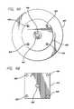
- FIG. 1illustrates generally a prior art technique for adjusting the orientation of a space transformer.
- a space transformer 110is shown with different sets of adjustment points on the bottom of space transformer 110 .
- the adjustment pointscorrespond to the locations of ball bearings that can be pressed against a back surface of space transformer 110 to adjust the orientation of space transformer 110 .
- three adjustment points 112 a - 112 care used to adjust the orientation of space transformer 110 .
- Adjustment points 112 a - 112 care located along the periphery of space transformer 110 .
- the adjustment points shown in FIG. 1can be used to deflect peripheral areas of space transformer 110 , but they cannot be used to deflect non-peripheral areas, such as the center, of space transformer 110 .
- the three points of adjustment shown in FIG. 1define a plane which is approximately parallel to the plane of a front surface of space transformer 110 . However, because there are only three adjustment points, they can adjust the orientation, but not the shape, of space transformer 110 ; geometric changes are made on only a low order (1 st order polynomial). Furthermore, using ball bearings in conjunction with the adjustment points provides for the application of only a pushing force against space transformer 110 , and in some instances, the pushing force is opposed by a spring member on an opposite side of space transformer 110 .
- the present inventionprovides, in one embodiment, a method of adjusting the planarity of a substrate in a probe card assembly, in which the method includes deflecting at least one of a first area of the substrate, a second area of the substrate, a third area of the substrate, and a fourth area of the substrate, and the deflecting includes applying a pulling force to at least one of the first, second, third and fourth areas of the substrate.
- the present inventionprovides, in another embodiment, a method of achieving a degree of planarity among contact portions of a plurality of contact structures mounted to a substrate, in which the method includes creating the substrate with the plurality of contact structures connected to a first surface of the substrate, the contact portions of the contact structures having a first planar relationship relative to one another, and applying a plurality of forces selectively to the substrate to deform the substrate and achieve a second planar relationship of the contact portions of the contact structures relative to one another
- FIG. 1illustrates generally a prior art technique for adjusting the planarity of a space transformer in a probe card assembly.
- FIG. 2illustrates a cross-sectional view of a probe card assembly in accordance with the teachings of the present invention.
- FIGS. 3A and 3Billustrate generally deflections of a substrate in a probe card assembly in accordance with the teachings of the present invention.
- FIG. 4Aillustrates a bottom view of a probe card assembly in accordance with the teachings of the present invention.
- FIG. 4Billustrates a bottom view of a substrate in the probe card assembly shown in FIG. 4A .
- FIGS. 5A-5Cillustrate different embodiments of a planarizing element for a probe card assembly in accordance with the teachings of the present invention.
- FIG. 6illustrates multiple adjustable substrates of a probe card assembly.
- FIG. 7Aillustrates a top view of a multiple substrate assembly in accordance with the teachings of the present invention.
- FIG. 7Billustrates a side view of the multiple substrate assembly shown in FIG. 7A .
- a probe card assemblyincludes a probe card, an interposer, a space transformer, a drive plate and a first control member.
- the interposeris located between the probe card and the space transformer.
- the drive plateis located adjacent to the probe card.
- a protrusionextends from a central area of the bottom surface of the space transformer and through a through hole in the interposer.
- the first control memberis coupled to the protrusion and is disposed within the through hole in the interposer and through holes in the probe card and drive plate.
- the first control memberhas an actuating component rotatably coupled to an end of the first control member that is accessible from an exposed side of the drive plate.
- a springis supported by the actuating component to be urged against the drive plate.
- the springis pressed against the drive plate and provides a resistance to the movement of the actuating component.
- the space transformeris pulled toward the interposer via the first control member coupled to the protrusion extending from the space transformer.
- a non-peripheral area of the space transformeris deflected according to a preferred embodiment of the present invention.
- FIG. 2illustrates a side cross-sectional view of a probe card assembly 200 in accordance with the teachings of the present invention.
- a space transformer 210is held down at its periphery by a clamping frame 212 .
- the top of space transformer 210may be substantially flush with the top of frame 212 such that a plurality of resilient contact structures 211 extending from the top of space transformer 210 can extend above the top surface of frame 212 .
- Contact structures 211each have a contact region for making contact with the terminals of an electronic component (e.g. bond pads on a semiconductor device).
- contact structures 211are free-standing, springable contact elements. It is appreciated that other contact elements can be used in place of contact structures 211 . It is preferred that such elements are sufficiently coupled to space transformer 210 to benefit from the planarizing action associated with the present invention. For example, posts, pins, pads, terminals and bumps/balls or other contact elements known in the art can be used as contact elements.
- a clamping spring 214(e.g. leaf spring) is coupled to a frame 218 by screws 216 .
- Spring 214secures frame 212 .
- a printed wiring board 220such as probe card, is located beneath frame 218 and has a through hole in its center and through holes at points around the center in a regular pattern.
- a drive plate 222which can also act as a stiffening substrate, is coupled to the bottom of board 220 .
- Drive plate 222has a set of through holes which align with the through holes in board 220 .
- Screws 224are placed in the outer through holes in both board 220 and drive plate 222 .
- Ball bearings 226rest on an end of screws 224 and are pressed against space transformer 210 when screws 224 are screwed toward space transformer 210 .
- An interposer 230is located between space transformer 210 and board 220 .
- Interposer 230has a central through hole.
- Resilient contact structures 229extend from the top of interposer 230 and effect pressure connections with contact pads 228 located on space transformer 210 .
- Resilient contact structures 231extend from the bottom of interposer 230 and effect pressure connections with contact terminals 234 located on board 220 .
- a threaded protrusion or stud 238extends from the bottom of space transformer 210 . Stud 238 may be coupled to space transformer 210 or integrally formed with space transformer 210 .
- An extension stud 240has a threaded bore in one end which is screwed onto stud 238 .
- Stud 240is threaded and accommodates an actuating nut 242 .
- Stud 240is disposed through the central through holes of interposer 230 , board 220 and drive plate 222 .
- a spring element 244e.g. Belleville washer
- a plurality of resilient contact structurescan be provided on the bottom surface of a space transformer (e.g. fabricated on the terminals on the bottom surface of a space transformer) to make direct contact to the terminals on the top surface of a printed wiring board.
- an interposeris optional.
- One alternative to an interposeris a semi-rigid support member that backs a flexible sheet incorporating contact structures.
- the semi-rigid support member, and hence the flexible sheet and contact structurescan be planarized in accordance with the teachings of the present invention.
- Other alternatives to an interposerinclude flex tape, pogo pins and other socket or interconnect constructions.
- planarity of space transformer 210can be adjusted via peripheral control members (e.g. screws 224 and ball bearings 226 ) and a non-peripheral control member (e.g. stud 240 coupled to stud 238 ).
- peripheral control memberse.g. screws 224 and ball bearings 226
- non-peripheral control membere.g. stud 240 coupled to stud 238 .
- screws 224can be accessed from the bottom side of drive plate 222 to drive them upward and force ball bearings 226 against space transformer 210 .
- space transformer 210is held by frame 212 and spring 214 , the contact of ball bearings 226 against space transformer 210 subjects space transformer 210 to compressive forces.
- space transformer 210deflects accordingly.
- ball bearings 226are located near the periphery of space transformer 210 , only peripheral areas of space transformer 210 are adjustable via screws 224 and ball bearings 226 .
- screws 224are accessible from an exposed side of drive plate 222 , the planarity of peripheral areas of space transformer 210 is remotely adjustable. It should be noted that screws 224 and ball bearings 226 can be used to deflect space transformer 210 without interfering with interposer 230 .
- a central area of space transformer 210can be deflected through the actuation of nut 242 .
- spring element 244is pressed against drive plate 222 by nut 242 .
- Spring element 244provides a resistance to the upward movement of nut 242 .
- stud 240is pulled down.
- the area of space transformer 210 where stud 238 is locatedis also pulled down along with stud 240 .
- such area of space transformer 210is subjected to a pulling force or tensile force.
- space transformer 210is bowed (e.g. domed)
- stud 240can be pulled down through the actuation of nut 242 to adjust the planarity of space transformer 210 .
- nut 242is accessible from an exposed side of drive plate 222 , the planarity of a non-peripheral area of space transformer 210 is remotely adjustable.
- studs 238 and 240can be used to deflect space transformer 210 without interfering with interposer 230 .
- Stud 238can be located at a variety of positions on the bottom surface of space transformer 210 .
- stud 238can be located near the center or the edge of the bottom surface of space transformer 210 .
- the planarizing apparatus of the present inventioncan be used to deflect peripheral areas, as well as non-peripheral areas, of a substrate in a probe card assembly.
- multiple studscan be used.
- a space transformercan be configured to use a system in which as many as all of the studs or other elements fixed to the space transformer provide pushing and pulling forces through an actuating mechanism to effect the desired deformation of a surface of the space transformer.
- Screws 224 and ball bearings 226cannot be used to pull down a central area of space transformer 210 because they are configured to function with an opposing spring against space transformer 210 .
- the planarizing apparatus of the present inventionaddresses such a deficiency as described above.
- the planarity of space transformer 210can be more thoroughly adjusted, particularly on a higher order of adjustment (e.g. 2 nd order polynomial, 3 rd order polynomial, etc.), with the planarizing apparatus of the present invention.
- the planarizing apparatus of the present inventioncan be used to deflect space transformer 210 such that the contact regions of contact structures 211 are planarized relative to one another.
- the planarization of the contact regions of contact structures 211allows more uniform contact to be made with the terminals of an electronic component to facilitate testing of the electronic component.
- the deflection of space transformer 210can effect more uniform contact between contact pads 228 and contact structures 229 , and between terminals 234 and contact structures 231 .
- FIGS. 3A and 3Billustrate generally a bowed substrate 310 , such as a space transformer, which is typically located in a probe card assembly.
- a force 332e.g. tensile force
- a central area of substrate 310can be deflected to a desired planarity.
- a force 334e.g.
- interposer 330which does not affect interposer 330 can be applied to substrate 310 to push substrate 310 into a desired position. Specifically, a central area of substrate 310 can be deflected to a desired planarity. Such a pushing force can be applied using an embodiment of the present invention as shown in FIG. 5C .
- FIG. 4Aillustrates a bottom view of a probe card assembly fitted with push-only control members 424 , which are similar to screws 224 , and a push-pull control member 440 , which is similar to extension stud 240 .
- a drive plate 422is coupled to a probe card 420 . Both drive plate 422 and probe card 420 have through holes to accommodate control members 424 and 440 .
- Control members 424drive ball bearings 426 at corresponding locations of a substrate 410 , as shown in FIG. 4B .
- Substrate 410such as a space transformer, is typically part of a probe card assembly such as that shown in FIG. 2 .
- a stud 428 extending from the surface of substrate 410is coupled to central control member 440 to allow a central area of substrate 410 to be deflected by the actuation of a nut 442 relative to control member 440 .
- Control members 424 and 440can be driven independently to adjust the planarity of substrate 410 in a variety of ways.
- FIGS. 5A-5Cillustrate various embodiments of a planarizing apparatus according to the present invention.
- a substrate 510such as a space transformer, has a stud 538 a coupled to or integrally formed with the bottom surface of substrate 510 .
- Stud 538 ahas a threaded bore to accommodate a connector 540 a having threaded ends.
- a nut 542 coupled to one of the threaded ends of connector 540 asupports a spring element 544 a , which can be pressed against a substrate (not shown), such as a drive plate, in a manner similar to that described in conjunction with FIG. 2 .
- Spring element 544 ais shown as a Belleville washer. It is appreciated that other springs elements, such as coil springs and wavy washers could be used in lieu of a Belleville washer. Furthermore, the spring element could be built into the bottom of the drive plate.
- substrate 510has a threaded stud 538 b coupled to or integrally formed with the bottom surface of substrate 510 .
- a connector 540 b with a threaded boreis coupled to stud 538 b .
- a nut 542 coupled to a threaded end of connector 540 bsupports spring elements 544 b - 544 d against a substrate (not shown), such as a drive plate.
- Different spring elementscan be used as spring elements 544 b - 544 d to provide varying resistances to nut 542 as nut 542 is twisted along the threads of connector 540 b toward space transformer 510 .
- substrate 510has a threaded stud 538 c coupled to or integrally formed with the bottom surface of substrate 510 .
- a connector 540 c with a threaded boreis coupled to stud 538 c .
- a threaded end of connector 540 cis coupled to a threaded through hole in a substrate 522 , such as drive plate.
- Connector 540 cis accessible from an exposed side of substrate 522 , which is typically an exterior substrate of a probe card assembly.
- Connector 540 ccan be turned clockwise or counter-clockwise to deflect substrate 510 in opposite directions.
- a multipoint adjustment schemecan also be used to modify the orientation (e.g. in x, y and ⁇ directions) of a substrate in a probe card assembly with respect to other substrates in the assembly without interfering with the planarity or orientation of such other substrates.
- a probe card assembly having multiple deformable substratesmay be constructed and made planar across the surface defined by their contact elements with respect to a test substrate, while appropriate positions of the contact elements from substrate to substrate are maintained. Such an assembly is shown generally in FIG. 6 .
- Multiple substrates 610 , 620 . . . nare located adjacent to one another in a combined assembly. Each substrate is adjustable with respect to the other substrates in x, y and ⁇ using orienting mechanisms (not shown) well known in the art. A system for deforming substrates in the z direction (out of the page) is also included but is not shown. Such a system may incorporate planarizing elements as disclosed herein.
- the vector rdefines the relationship between corresponding contact elements 610 a, 620 a . . . z on multiple substrates 610 , 620 . . . n, respectively. Substrates 610 , 620 . . .
- nare positioned with respect to one another such that r is within a desired degree of accuracy, and deformed such that the contact tips of contact elements 610 a , 620 a . . . z are coplanar within a desired degree of accuracy in the z direction.
- contact elements 711are secured to insulating support member 705 .
- Contact elements 711are electrically connected by traces 706 to connecting wires 715 , which are connected in turn to traces 713 and to tester 760 .
- Contact elements 711are illustrated as solder balls but of course can take many of the forms described herein.
- connecting wires 715are portions of a multi-stranded flex cable.
- connecting wires 715can be wirebonded connections.
- insulating support member 705is polyimide, or other flex materials well known in the art.
- Substrate 704supports insulating support member 705 . In one preferred embodiment, they are secured together. In another preferred embodiment, they can be in close contact, but can move relative to each other. Substrate 704 is positioned by a push-only control element comprising actuator 730 acting on element 724 and ball 726 to press against substrate 704 , opposed by spring 712 , which in turn is secured to substrate frame 720 . Several of these push control elements can be used; two are shown in FIG. 7B for illustrative purposes. Substrate 704 also is positioned by a push-pull control element comprising actuator 732 , element 740 , and stud 738 , which is secured to substrate 704 . Substrate frame 720 is secured to substrate housing 722 , which in turn is connected to actuators 730 , 732 , forming a closed loop system. By selectively positioning the actuators, the shape of substrate 704 can be controlled.
- Printed wiring board 750supports housing 752 , which is connected to positioning element 756 , which in turn is connected to substrate housing 722 directly or, as shown, through bridge housing 754 .
- Positioning element 756is illustrated in stylized form and can include elements as desired to provide x, y, z, and three degrees of positional control over substrate housing 722 .
- FIG. 7Billustrates a second substrate 704 a as well, with elements as described above.
- Each substrate 704 , 704 acan be adjusted to a desired degree of planarity. Equally well, each substrate 704 , 704 a can be adjusted to a desired degree of flatness of the contact region portion of each of contact elements 711 .
- substrates 704 and 704 Acan be positioned relative to each other to provide a relatively large array of contact elements 711 .
- Such a probe card assembly constructed of multiple deformable substratesis functionally equivalent to a larger probe card assembly having a much larger (equivalent in area) single substrate. It is important to note that deformation of the monolithic substrate in order to change the spatial relationship of the contact elements residing on it is achieved both by deformation and x, y, z, and ⁇ movement of the multiple substrates and supporting structures in which they reside.
- the planarizing apparatus of the present inventioncan be manually actuated or automatically actuated.
- an actuator mechanismcan be connected to a planarizing apparatus (e.g. to the actuating nut) and operated according to signals from a computer system.
- a greater number of control points driven by such automated planarizing apparatusescan shape a substrate to a higher degree of accuracy.
Landscapes
- Physics & Mathematics (AREA)
- General Physics & Mathematics (AREA)
- Measuring Leads Or Probes (AREA)
- Testing Or Measuring Of Semiconductors Or The Like (AREA)
Abstract
Description
Claims (14)
Priority Applications (1)
| Application Number | Priority Date | Filing Date | Title |
|---|---|---|---|
| US13/092,709US8427183B2 (en) | 2000-03-17 | 2011-04-22 | Probe card assembly having an actuator for bending the probe substrate |
Applications Claiming Priority (3)
| Application Number | Priority Date | Filing Date | Title |
|---|---|---|---|
| US52793100A | 2000-03-17 | 2000-03-17 | |
| US12/766,101US20100263432A1 (en) | 2000-03-17 | 2010-04-23 | Methods for planarizing a semiconductor contactor |
| US13/092,709US8427183B2 (en) | 2000-03-17 | 2011-04-22 | Probe card assembly having an actuator for bending the probe substrate |
Related Parent Applications (1)
| Application Number | Title | Priority Date | Filing Date |
|---|---|---|---|
| US12/766,101DivisionUS20100263432A1 (en) | 2000-03-17 | 2010-04-23 | Methods for planarizing a semiconductor contactor |
Publications (2)
| Publication Number | Publication Date |
|---|---|
| US20110193583A1 US20110193583A1 (en) | 2011-08-11 |
| US8427183B2true US8427183B2 (en) | 2013-04-23 |
Family
ID=33539390
Family Applications (4)
| Application Number | Title | Priority Date | Filing Date |
|---|---|---|---|
| US10/852,370Expired - LifetimeUS7262611B2 (en) | 2000-03-17 | 2004-05-24 | Apparatuses and methods for planarizing a semiconductor contactor |
| US11/846,012Expired - Fee RelatedUS7737709B2 (en) | 2000-03-17 | 2007-08-28 | Methods for planarizing a semiconductor contactor |
| US12/766,101AbandonedUS20100263432A1 (en) | 2000-03-17 | 2010-04-23 | Methods for planarizing a semiconductor contactor |
| US13/092,709Expired - LifetimeUS8427183B2 (en) | 2000-03-17 | 2011-04-22 | Probe card assembly having an actuator for bending the probe substrate |
Family Applications Before (3)
| Application Number | Title | Priority Date | Filing Date |
|---|---|---|---|
| US10/852,370Expired - LifetimeUS7262611B2 (en) | 2000-03-17 | 2004-05-24 | Apparatuses and methods for planarizing a semiconductor contactor |
| US11/846,012Expired - Fee RelatedUS7737709B2 (en) | 2000-03-17 | 2007-08-28 | Methods for planarizing a semiconductor contactor |
| US12/766,101AbandonedUS20100263432A1 (en) | 2000-03-17 | 2010-04-23 | Methods for planarizing a semiconductor contactor |
Country Status (1)
| Country | Link |
|---|---|
| US (4) | US7262611B2 (en) |
Cited By (5)
| Publication number | Priority date | Publication date | Assignee | Title |
|---|---|---|---|---|
| US20110254577A1 (en)* | 2010-04-16 | 2011-10-20 | Taiwan Semiconductor Manufacturing Company, Ltd. | Non-Reflow Probe Card Structure |
| US20120042516A1 (en)* | 2010-08-19 | 2012-02-23 | Kabushiki Kaisha Nihon Micronics | Method for manufacturing probe card |
| US20120042509A1 (en)* | 2010-08-19 | 2012-02-23 | Kabushiki Kaisha Nihon Micronics | Method for manufacturing probe card |
| US20130340936A1 (en)* | 2012-02-22 | 2013-12-26 | Expresslo Llc | Method for ex-situ lift-out specimen preparation |
| US10295564B2 (en) | 2016-07-18 | 2019-05-21 | Samsung Electronics Co., Ltd. | Apparatus for clamping a probe card and probe card including the same |
Families Citing this family (26)
| Publication number | Priority date | Publication date | Assignee | Title |
|---|---|---|---|---|
| US7262611B2 (en) | 2000-03-17 | 2007-08-28 | Formfactor, Inc. | Apparatuses and methods for planarizing a semiconductor contactor |
| US7285968B2 (en)* | 2005-04-19 | 2007-10-23 | Formfactor, Inc. | Apparatus and method for managing thermally induced motion of a probe card assembly |
| US7762822B2 (en) | 2005-04-27 | 2010-07-27 | Aehr Test Systems | Apparatus for testing electronic devices |
| US7471094B2 (en)* | 2005-06-24 | 2008-12-30 | Formfactor, Inc. | Method and apparatus for adjusting a multi-substrate probe structure |
| DE112005003731B4 (en)* | 2005-10-24 | 2013-04-18 | Kabushiki Kaisha Nihon Micronics | Method for mounting an electrical connection device |
| US7504822B2 (en)* | 2005-10-28 | 2009-03-17 | Teradyne, Inc. | Automatic testing equipment instrument card and probe cabling system and apparatus |
| US7541819B2 (en)* | 2005-10-28 | 2009-06-02 | Teradyne, Inc. | Modularized device interface with grounding insert between two strips |
| US7622935B2 (en)* | 2005-12-02 | 2009-11-24 | Formfactor, Inc. | Probe card assembly with a mechanically decoupled wiring substrate |
| US7671614B2 (en)* | 2005-12-02 | 2010-03-02 | Formfactor, Inc. | Apparatus and method for adjusting an orientation of probes |
| US7180316B1 (en)* | 2006-02-03 | 2007-02-20 | Touchdown Technologies, Inc. | Probe head with machined mounting pads and method of forming same |
| US7368930B2 (en)* | 2006-08-04 | 2008-05-06 | Formfactor, Inc. | Adjustment mechanism |
| US20080036483A1 (en)* | 2006-08-08 | 2008-02-14 | Taiwan Semiconductor Manufacturing Co., Ltd. | Probe card for flip chip testing |
| US7825675B2 (en)* | 2006-11-01 | 2010-11-02 | Formfactor, Inc. | Method and apparatus for providing active compliance in a probe card assembly |
| US7471078B2 (en)* | 2006-12-29 | 2008-12-30 | Formfactor, Inc. | Stiffener assembly for use with testing devices |
| US7884627B2 (en)* | 2006-12-29 | 2011-02-08 | Formfactor, Inc. | Stiffener assembly for use with testing devices |
| WO2008120302A1 (en)* | 2007-03-28 | 2008-10-09 | Fujitsu Microelectronics Limited | Test device for semiconductor device |
| US7791361B2 (en)* | 2007-12-10 | 2010-09-07 | Touchdown Technologies, Inc. | Planarizing probe card |
| US7800382B2 (en) | 2007-12-19 | 2010-09-21 | AEHR Test Ststems | System for testing an integrated circuit of a device and its method of use |
| US8528885B2 (en)* | 2008-04-21 | 2013-09-10 | Formfactor, Inc. | Multi-stage spring system |
| US7960989B2 (en)* | 2008-12-03 | 2011-06-14 | Formfactor, Inc. | Mechanical decoupling of a probe card assembly to improve thermal response |
| KR101583000B1 (en)* | 2009-03-09 | 2016-01-19 | 삼성전자주식회사 | Semiconductor device test apparatus and method |
| US8030957B2 (en)* | 2009-03-25 | 2011-10-04 | Aehr Test Systems | System for testing an integrated circuit of a device and its method of use |
| US9581639B2 (en)* | 2013-12-28 | 2017-02-28 | Intel Corporation | Organic space transformer attachment and assembly |
| TWI836645B (en) | 2016-01-08 | 2024-03-21 | 美商艾爾測試系統 | Tester apparatus and method of testing microelectronic device |
| KR20250122540A (en) | 2017-03-03 | 2025-08-13 | 에어 테스트 시스템즈 | Cartridge, test piece and method of testing one or more electronic devices |
| EP4226165A4 (en) | 2020-10-07 | 2024-10-30 | AEHR Test Systems | Electronics tester |
Citations (179)
| Publication number | Priority date | Publication date | Assignee | Title |
|---|---|---|---|---|
| US2729040A (en) | 1954-02-10 | 1956-01-03 | Boeing Co | Vacuum chuck jigs |
| US3623127A (en) | 1969-11-03 | 1971-11-23 | Ashley C Glenn | Electrical printed circuit switching device |
| US3634807A (en) | 1969-03-28 | 1972-01-11 | Siemens Ag | Detachable electrical contact arrangement |
| US3702439A (en) | 1970-08-12 | 1972-11-07 | Bell Telephone Labor Inc | Low impedance fixed point test probe |
| US3795037A (en) | 1970-05-05 | 1974-03-05 | Int Computers Ltd | Electrical connector devices |
| US3806801A (en) | 1972-12-26 | 1974-04-23 | Ibm | Probe contactor having buckling beam probes |
| US3866119A (en) | 1973-09-10 | 1975-02-11 | Probe Rite Inc | Probe head-probing machine coupling adaptor |
| US3952410A (en) | 1974-03-28 | 1976-04-27 | Xynetics, Inc. | Probe card including a multiplicity of probe contacts and method of making |
| US3963986A (en) | 1975-02-10 | 1976-06-15 | International Business Machines Corporation | Programmable interface contactor structure |
| US3998377A (en) | 1974-12-09 | 1976-12-21 | Teletype Corporation | Method of and apparatus for bonding workpieces |
| US4038599A (en) | 1974-12-30 | 1977-07-26 | International Business Machines Corporation | High density wafer contacting and test system |
| US4116523A (en) | 1976-01-23 | 1978-09-26 | James M. Foster | High frequency probe |
| US4161692A (en) | 1977-07-18 | 1979-07-17 | Cerprobe Corporation | Probe device for integrated circuit wafers |
| US4177554A (en) | 1978-04-26 | 1979-12-11 | Western Electric Co., Inc. | Assembling leads to a substrate |
| US4312117A (en) | 1977-09-01 | 1982-01-26 | Raytheon Company | Integrated test and assembly device |
| US4423376A (en) | 1981-03-20 | 1983-12-27 | International Business Machines Corporation | Contact probe assembly having rotatable contacting probe elements |
| US4506215A (en) | 1981-06-30 | 1985-03-19 | International Business Machines Corporation | Modular test probe |
| US4518914A (en) | 1981-08-03 | 1985-05-21 | Japan Electronic Materials Corportion | Testing apparatus of semiconductor wafers |
| US4523133A (en) | 1982-01-13 | 1985-06-11 | Computer Peripherals Inc. | Tape transport system with tension sensing bearings |
| US4536470A (en) | 1982-09-07 | 1985-08-20 | International Business Machines Corporation | Method and apparatus for making a mask conforming to a ceramic substrate metallization pattern |
| US4567433A (en) | 1980-05-27 | 1986-01-28 | Nihon Denshi Zairo Kabushiki Kaisha | Complex probe card for testing a semiconductor wafer |
| US4599559A (en) | 1983-05-03 | 1986-07-08 | Wentworth Laboratories, Inc. | Test probe assembly for IC chips |
| US4622514A (en) | 1984-06-15 | 1986-11-11 | Ibm | Multiple mode buckling beam probe assembly |
| US4623839A (en) | 1982-09-17 | 1986-11-18 | Angliatech Limited | Probe device for testing an integrated circuit |
| US4636722A (en) | 1984-05-21 | 1987-01-13 | Probe-Rite, Inc. | High density probe-head with isolated and shielded transmission lines |
| US4650545A (en) | 1985-02-19 | 1987-03-17 | Tektronix, Inc. | Polyimide embedded conductor process |
| US4665360A (en) | 1985-03-11 | 1987-05-12 | Eaton Corporation | Docking apparatus |
| US4734046A (en) | 1984-09-21 | 1988-03-29 | International Business Machines Corporation | Coaxial converter with resilient terminal |
| US4751457A (en) | 1986-09-08 | 1988-06-14 | Tektronix, Inc. | Integrated circuit probe parallelism establishing method and apparatus |
| US4757256A (en) | 1985-05-10 | 1988-07-12 | Micro-Probe, Inc. | High density probe card |
| US4758785A (en) | 1986-09-03 | 1988-07-19 | Tektronix, Inc. | Pressure control apparatus for use in an integrated circuit testing station |
| EP0275634A1 (en) | 1986-12-15 | 1988-07-27 | Trw Inc. | Integrated-circuit chip test probe card |
| US4784972A (en) | 1984-08-18 | 1988-11-15 | Matsushita Electric Industrial Co. Ltd. | Method of joining beam leads with projections to device electrodes |
| US4793814A (en) | 1986-07-21 | 1988-12-27 | Rogers Corporation | Electrical circuit board interconnect |
| US4833402A (en) | 1984-06-13 | 1989-05-23 | Boegh Petersen Allan | Connector assembly for a circuit board testing machine, a circuit board testing machine, and a method of testing a circuit board by means of a circuit board testing machine |
| US4837622A (en) | 1985-05-10 | 1989-06-06 | Micro-Probe, Inc. | High density probe card |
| US4866507A (en) | 1986-05-19 | 1989-09-12 | International Business Machines Corporation | Module for packaging semiconductor integrated circuit chips on a base substrate |
| US4891585A (en) | 1986-09-05 | 1990-01-02 | Tektronix, Inc. | Multiple lead probe for integrated circuits in wafer form |
| US4899099A (en) | 1988-05-19 | 1990-02-06 | Augat Inc. | Flex dot wafer probe |
| US4906920A (en) | 1988-10-11 | 1990-03-06 | Hewlett-Packard Company | Self-leveling membrane probe |
| US4922192A (en) | 1988-09-06 | 1990-05-01 | Unisys Corporation | Elastic membrane probe |
| US4943719A (en) | 1989-01-17 | 1990-07-24 | The Board Of Trustees Of The Leland Stanford University | Microminiature cantilever stylus |
| US4947481A (en) | 1987-05-09 | 1990-08-07 | Pioneer Electronic Corporation | Information reader for disk player |
| EP0295914A3 (en) | 1987-06-19 | 1990-09-26 | Hewlett-Packard Company | An interconnect structure for pc boards and integrated circuits |
| US4961052A (en) | 1989-01-07 | 1990-10-02 | Mitsubishi Denki Kabushiki Kaisha | Probing plate for wafer testing |
| US4965865A (en) | 1989-10-11 | 1990-10-23 | General Signal Corporation | Probe card for integrated circuit chip |
| US4968589A (en) | 1988-10-26 | 1990-11-06 | General Signal Corporation | Probe card for integrated circuit chip and method of making probe card |
| US4969826A (en) | 1989-12-06 | 1990-11-13 | Amp Incorporated | High density connector for an IC chip carrier |
| US4975638A (en) | 1989-12-18 | 1990-12-04 | Wentworth Laboratories | Test probe assembly for testing integrated circuit devices |
| US4998062A (en)* | 1988-10-25 | 1991-03-05 | Tokyo Electron Limited | Probe device having micro-strip line structure |
| US4998885A (en) | 1989-10-27 | 1991-03-12 | International Business Machines Corporation | Elastomeric area array interposer |
| US5049084A (en) | 1989-12-05 | 1991-09-17 | Rogers Corporation | Electrical circuit board interconnect |
| US5055778A (en) | 1989-10-02 | 1991-10-08 | Nihon Denshizairyo Kabushiki Kaisha | Probe card in which contact pressure and relative position of each probe end are correctly maintained |
| US5059898A (en) | 1990-08-09 | 1991-10-22 | Tektronix, Inc. | Wafer probe with transparent loading member |
| US5066358A (en) | 1988-10-27 | 1991-11-19 | Board Of Trustees Of The Leland Stanford Juninor University | Nitride cantilevers with single crystal silicon tips |
| US5070297A (en) | 1990-06-04 | 1991-12-03 | Texas Instruments Incorporated | Full wafer integrated circuit testing device |
| US5094536A (en) | 1990-11-05 | 1992-03-10 | Litel Instruments | Deformable wafer chuck |
| US5095616A (en) | 1990-10-26 | 1992-03-17 | Tektronix, Inc. | Grounding method for use in high frequency electrical circuitry |
| US5103557A (en) | 1988-05-16 | 1992-04-14 | Leedy Glenn J | Making and testing an integrated circuit using high density probe points |
| US5120572A (en) | 1990-10-30 | 1992-06-09 | Microelectronics And Computer Technology Corporation | Method of fabricating electrical components in high density substrates |
| US5148103A (en) | 1990-10-31 | 1992-09-15 | Hughes Aircraft Company | Apparatus for testing integrated circuits |
| US5152695A (en) | 1991-10-10 | 1992-10-06 | Amp Incorporated | Surface mount electrical connector |
| US5157325A (en) | 1991-02-15 | 1992-10-20 | Compaq Computer Corporation | Compact, wireless apparatus for electrically testing printed circuit boards |
| US5166520A (en) | 1991-05-13 | 1992-11-24 | The Regents Of The University Of California | Universal, microfabricated probe for scanning probe microscopes |
| US5173055A (en) | 1991-08-08 | 1992-12-22 | Amp Incorporated | Area array connector |
| US5180977A (en) | 1991-12-02 | 1993-01-19 | Hoya Corporation Usa | Membrane probe contact bump compliancy system |
| US5221415A (en) | 1989-01-17 | 1993-06-22 | Board Of Trustees Of The Leland Stanford Junior University | Method of forming microfabricated cantilever stylus with integrated pyramidal tip |
| US5225771A (en) | 1988-05-16 | 1993-07-06 | Dri Technology Corp. | Making and testing an integrated circuit using high density probe points |
| US5228862A (en) | 1992-08-31 | 1993-07-20 | International Business Machines Corporation | Fluid pressure actuated connector |
| US5260926A (en) | 1991-04-22 | 1993-11-09 | Canon Kabushiki Kaisha | Atomic force microscope with a plurality of cantilevers for recording/reproducing information |
| US5264696A (en) | 1991-05-20 | 1993-11-23 | Olympus Optical Co., Ltd. | Cantilever chip for scanning probe microscope having first and second probes formed with different aspect ratios |
| FR2680284B1 (en) | 1991-08-09 | 1993-12-03 | Thomson Csf | VERY LOW PIT CONNECTION DEVICE AND MANUFACTURING METHOD. |
| US5272913A (en) | 1990-08-31 | 1993-12-28 | Olympus Optical Co., Ltd. | Cantilever for a scanning probe microscope and a method of manufacturing the same |
| US5321453A (en) | 1991-08-03 | 1994-06-14 | Tokyo Electron Limited | Probe apparatus for probing an object held above the probe card |
| US5323107A (en) | 1991-04-15 | 1994-06-21 | Hitachi America, Ltd. | Active probe card |
| US5355079A (en) | 1993-01-07 | 1994-10-11 | Wentworth Laboratories, Inc. | Probe assembly for testing integrated circuit devices |
| US5371654A (en) | 1992-10-19 | 1994-12-06 | International Business Machines Corporation | Three dimensional high performance interconnection package |
| EP0460822B1 (en) | 1990-06-04 | 1994-12-28 | International Business Machines Corporation | Integrated circuit packaging using flexible substrate |
| US5416429A (en) | 1994-05-23 | 1995-05-16 | Wentworth Laboratories, Inc. | Probe assembly for testing integrated circuits |
| US5422574A (en) | 1993-01-14 | 1995-06-06 | Probe Technology Corporation | Large scale protrusion membrane for semiconductor devices under test with very high pin counts |
| US5450290A (en) | 1993-02-01 | 1995-09-12 | International Business Machines Corporation | Printed circuit board with aligned connections and method of making same |
| US5461326A (en) | 1993-02-25 | 1995-10-24 | Hughes Aircraft Company | Self leveling and self tensioning membrane test probe |
| US5476211A (en) | 1993-11-16 | 1995-12-19 | Form Factor, Inc. | Method of manufacturing electrical contacts, using a sacrificial member |
| US5476818A (en) | 1994-08-19 | 1995-12-19 | Motorola, Inc. | Semiconductor structure and method of manufacture |
| US5480503A (en) | 1993-12-30 | 1996-01-02 | International Business Machines Corporation | Process for producing circuitized layers and multilayer ceramic sub-laminates and composites thereof |
| US5491426A (en) | 1994-06-30 | 1996-02-13 | Vlsi Technology, Inc. | Adaptable wafer probe assembly for testing ICs with different power/ground bond pad configurations |
| US5513430A (en) | 1994-08-19 | 1996-05-07 | Motorola, Inc. | Method for manufacturing a probe |
| US5517126A (en) | 1993-03-18 | 1996-05-14 | Tokyo Electron Limited | Probe apparatus |
| US5517280A (en) | 1994-04-12 | 1996-05-14 | The Board Of Trustees Of The Leland Stanford, Jr. University | Photolithography system |
| WO1996015458A1 (en)* | 1994-11-15 | 1996-05-23 | Formfactor, Inc. | Probe card assembly and kit, and methods of using same |
| US5521518A (en) | 1990-09-20 | 1996-05-28 | Higgins; H. Dan | Probe card apparatus |
| US5521522A (en) | 1992-11-13 | 1996-05-28 | Tokyo Electron Limited | Probe apparatus for testing multiple integrated circuit dies |
| US5530371A (en) | 1994-04-15 | 1996-06-25 | International Business Machines Corporation | Probe card assembly |
| US5534784A (en) | 1994-05-02 | 1996-07-09 | Motorola, Inc. | Method for probing a semiconductor wafer |
| US5541525A (en) | 1991-06-04 | 1996-07-30 | Micron Technology, Inc. | Carrier for testing an unpackaged semiconductor die |
| US5563509A (en) | 1994-06-30 | 1996-10-08 | Vlsi Technology, Inc. | Adaptable load board assembly for testing ICs with different power/ground bond pad and/or pin configurations |
| US5576630A (en) | 1993-06-16 | 1996-11-19 | Nitto Denko Corporation | Probe structure for measuring electric characteristics of a semiconductor element |
| US5613861A (en) | 1995-06-07 | 1997-03-25 | Xerox Corporation | Photolithographically patterned spring contact |
| US5639385A (en) | 1992-06-04 | 1997-06-17 | Lsi Logic Corporation | Method of fabricating a wafer probe card for testing an integrated circuit die |
| US5642054A (en) | 1995-08-08 | 1997-06-24 | Hughes Aircraft Company | Active circuit multi-port membrane probe for full wafer testing |
| US5642056A (en) | 1993-12-22 | 1997-06-24 | Tokyo Electron Limited | Probe apparatus for correcting the probe card posture before testing |
| US5649385A (en) | 1994-09-16 | 1997-07-22 | Acevedo; Michael J. | Insect trap and method |
| US5654647A (en) | 1995-02-03 | 1997-08-05 | Hewlett-Packard Company | Multiple lead voltage probe and method of making same |
| US5672977A (en) | 1994-09-09 | 1997-09-30 | Tokyo Electron Limited | Probe apparatus |
| EP0845677A1 (en) | 1996-11-08 | 1998-06-03 | W.L. GORE & ASSOCIATES, INC. | A method of using a temporary z-axis material |
| US5774340A (en) | 1996-08-28 | 1998-06-30 | International Business Machines Corporation | Planar redistribution structure and printed wiring device |
| US5786701A (en) | 1993-07-02 | 1998-07-28 | Mitel Semiconductor Limited | Bare die testing |
| EP0802419A3 (en) | 1996-04-15 | 1998-08-12 | Nec Corporation | Probe card and method of forming the same |
| US5801441A (en) | 1994-07-07 | 1998-09-01 | Tessera, Inc. | Microelectronic mounting with multiple lead deformation and bonding |
| US5806181A (en) | 1993-11-16 | 1998-09-15 | Formfactor, Inc. | Contact carriers (tiles) for populating larger substrates with spring contacts |
| US5815961A (en) | 1996-06-26 | 1998-10-06 | Whirlpool Corporation | Clothes treating cabinet with inflatable hanger |
| US5825192A (en) | 1995-07-14 | 1998-10-20 | Tokyo Electron Limited | Probe card device used in probing apparatus |
| US5828226A (en) | 1996-11-06 | 1998-10-27 | Cerprobe Corporation | Probe card assembly for high density integrated circuits |
| US5847571A (en) | 1994-09-09 | 1998-12-08 | Micromodule Systems | Membrane probing of circuits |
| US5861759A (en) | 1997-01-29 | 1999-01-19 | Tokyo Electron Limited | Automatic probe card planarization system |
| US5879568A (en) | 1996-06-18 | 1999-03-09 | Hitachi, Ltd. | Process for producing multilayer printed circuit board for wire bonding |
| US5914533A (en) | 1995-06-06 | 1999-06-22 | International Business Machines Corporation | Multilayer module with thinfilm redistribution area |
| US5917707A (en) | 1993-11-16 | 1999-06-29 | Formfactor, Inc. | Flexible contact structure with an electrically conductive shell |
| US5937515A (en) | 1995-04-25 | 1999-08-17 | Johnson; Morgan T. | Reconfigurable circuit fabrication method |
| US5952840A (en) | 1996-12-31 | 1999-09-14 | Micron Technology, Inc. | Apparatus for testing semiconductor wafers |
| US5974662A (en) | 1993-11-16 | 1999-11-02 | Formfactor, Inc. | Method of planarizing tips of probe elements of a probe card assembly |
| US5976286A (en) | 1997-10-14 | 1999-11-02 | International Business Machines Corporation | Multi-density ceramic structure and process thereof |
| EP0701135B1 (en) | 1994-08-19 | 1999-11-17 | Hughes Electronics Corporation | Single-wafer tunneling sensor and low-cost IC manufacturing method |
| US5989994A (en) | 1998-12-29 | 1999-11-23 | Advantest Corp. | Method for producing contact structures |
| US5990695A (en) | 1998-01-16 | 1999-11-23 | Packard Hughes Interconnect Co. | Membrane test probe |
| US6011405A (en) | 1997-10-28 | 2000-01-04 | Qualitau, Inc. | Apparatus and method for probing multiple integrated circuit dice in a semiconductor wafer |
| US6021050A (en) | 1998-12-02 | 2000-02-01 | Bourns, Inc. | Printed circuit boards with integrated passive components and method for making same |
| US6028305A (en) | 1998-03-25 | 2000-02-22 | Board Of Trustees Of The Leland Stanford Jr. University | Dual cantilever scanning probe microscope |
| US6029966A (en) | 1998-10-13 | 2000-02-29 | Hertz; Allen D. | Flexible, self conforming, workpiece support system |
| US6040700A (en) | 1997-09-15 | 2000-03-21 | Credence Systems Corporation | Semiconductor tester system including test head supported by wafer prober frame |
| US6043668A (en) | 1997-12-12 | 2000-03-28 | Sony Corporation | Planarity verification system for integrated circuit test probes |
| US6072190A (en) | 1995-11-22 | 2000-06-06 | Advantest Corp. | Micro contact pin structure with a piezoelectric element and probe card using the same |
| US6078186A (en) | 1997-12-31 | 2000-06-20 | Micron Technology, Inc. | Force applying probe card and test system for semiconductor wafers |
| US6087840A (en) | 1997-10-21 | 2000-07-11 | Mitsubishi Denki Kabushiki Kaisha | Probe card with vertical needle for enabling improved wafer testing and method of manufacturing the same |
| JP3065659B2 (en) | 1989-07-25 | 2000-07-17 | ファルマシア・アンド・アップジョン・カンパニー | Antiarrhythmic tertiary amine-alkenyl-phenyl-alkanesulfonamide |
| US6122823A (en) | 1997-09-12 | 2000-09-26 | Fujitsu Limited | Apparatus to produce a multichip package module in which rough-pitch and fine-pitch chips are mounted on a board |
| US6140830A (en) | 1995-03-01 | 2000-10-31 | Test Plus Electronic Gmbh | Adapter system for component assembly circuit boards, for use in a test device |
| US6144212A (en) | 1997-10-21 | 2000-11-07 | Mitsubishi Denki Kabushiki Kaisha | Vertical needle type probe card, method of manufacturing thereof, method of replacing defective probe needle and test method of wafer using the probe card |
| US6160412A (en) | 1998-11-05 | 2000-12-12 | Wentworth Laboratories, Inc. | Impedance-matched interconnection device for connecting a vertical-pin integrated circuit probing device to integrated circuit test equipment |
| US6166552A (en) | 1996-06-10 | 2000-12-26 | Motorola Inc. | Method and apparatus for testing a semiconductor wafer |
| US6189876B1 (en) | 1998-05-05 | 2001-02-20 | Mcms, Inc. | Method and apparatus for leveling the upper surface of a PCB |
| US6193910B1 (en) | 1997-11-11 | 2001-02-27 | Ngk Spark Plug Co., Ltd. | Paste for through-hole filling and printed wiring board using the same |
| US6232791B1 (en) | 1998-10-27 | 2001-05-15 | Matsushita Electric Industrial Co., Ltd. | Testing Board |
| US6241838B1 (en) | 1997-09-08 | 2001-06-05 | Murata Manufacturing Co., Ltd. | Method of producing a multi-layer ceramic substrate |
| EP1014096A3 (en) | 1998-12-21 | 2001-06-27 | Shinko Electric Industries Co. Ltd. | Substrate and method for inspection |
| US6255602B1 (en) | 1999-03-15 | 2001-07-03 | Wentworth Laboratories, Inc. | Multiple layer electrical interface |
| US6272020B1 (en) | 1997-10-16 | 2001-08-07 | Hitachi, Ltd. | Structure for mounting a semiconductor device and a capacitor device on a substrate |
| US6275051B1 (en) | 1997-12-29 | 2001-08-14 | International Business Machines Corporation | Segmented architecture for wafer test and burn-in |
| US6305230B1 (en) | 1997-05-09 | 2001-10-23 | Hitachi, Ltd. | Connector and probing system |
| US6341417B1 (en) | 1999-09-23 | 2002-01-29 | International Business Machines Corporation | Pre-patterned substrate layers for being personalized as needed |
| JP3292406B2 (en) | 1993-07-15 | 2002-06-17 | 株式会社ジオトップ | Method and apparatus for connecting tension rod to reinforced cage |
| US6420884B1 (en) | 1999-01-29 | 2002-07-16 | Advantest Corp. | Contact structure formed by photolithography process |
| US6483328B1 (en)* | 1995-11-09 | 2002-11-19 | Formfactor, Inc. | Probe card for probing wafers with raised contact elements |
| US6499216B1 (en) | 1994-07-07 | 2002-12-31 | Tessera, Inc. | Methods and structures for electronic probing arrays |
| US6509751B1 (en)* | 2000-03-17 | 2003-01-21 | Formfactor, Inc. | Planarizer for a semiconductor contactor |
| US6586956B2 (en) | 2000-05-31 | 2003-07-01 | Advantest, Corp. | Probe contract system having planarity adjustment mechanism |
| DE19952943C2 (en) | 1999-11-03 | 2003-07-03 | Infineon Technologies Ag | Needle card adjustment device for the planarization of needle sets of a needle card |
| US6676784B2 (en) | 2001-07-17 | 2004-01-13 | International Business Machines Corporation | Process for the manufacture of multilayer ceramic substrates |
| US6706975B2 (en) | 2000-07-13 | 2004-03-16 | Ngk Spark Plug Co., Ltd. | Paste for filling throughhole and printed wiring board using same |
| US6727714B2 (en)* | 2001-09-27 | 2004-04-27 | Renesas Technology Corp. | Probe card |
| US6726195B1 (en) | 1998-10-13 | 2004-04-27 | Dek International Gmbh | Method for ensuring planarity when using a flexible, self conforming, workpiece support system |
| US6729019B2 (en) | 2001-07-11 | 2004-05-04 | Formfactor, Inc. | Method of manufacturing a probe card |
| US6774651B1 (en) | 1997-11-24 | 2004-08-10 | Micron Technology, Inc. | Method for aligning and connecting semiconductor components to substrates |
| US6784678B2 (en) | 2000-08-04 | 2004-08-31 | Infineon Technologies Ag | Test apparatus for semiconductor circuit and method of testing semiconductor circuits |
| US6799976B1 (en) | 1999-07-28 | 2004-10-05 | Nanonexus, Inc. | Construction structures and manufacturing processes for integrated circuit wafer probe card assemblies |
| US6894888B2 (en) | 2001-06-07 | 2005-05-17 | Ngk Insulators, Ltd. | Multilayer board having precise perforations and circuit substrate having precise through-holes |
| US6917525B2 (en) | 2001-11-27 | 2005-07-12 | Nanonexus, Inc. | Construction structures and manufacturing processes for probe card assemblies and packages having wafer level springs |
| US20060049820A1 (en) | 2004-09-09 | 2006-03-09 | Formfactor, Inc. | Method and apparatus for remotely buffering test channels |
| US7098650B2 (en) | 2003-07-28 | 2006-08-29 | Nextest Systems Corporation | Apparatus for planarizing a probe card and method using same |
| US7102085B2 (en) | 2001-03-23 | 2006-09-05 | Ngk Spark Plug Co., Ltd. | Wiring substrate |
| US7129723B2 (en) | 2004-05-28 | 2006-10-31 | Feinmetall Gmbh | Test device for electrical testing of a unit under test |
| US7129730B2 (en) | 2004-12-15 | 2006-10-31 | Chipmos Technologies (Bermuda) Ltd. | Probe card assembly |
| US7154284B2 (en) | 2004-07-28 | 2006-12-26 | Mjc Probe Incorporation | Integrated circuit probe card |
| US20060290367A1 (en) | 2005-06-24 | 2006-12-28 | Formfactor, Inc. | Method and apparatus for adjusting a multi-substrate probe structure |
| US7262611B2 (en)* | 2000-03-17 | 2007-08-28 | Formfactor, Inc. | Apparatuses and methods for planarizing a semiconductor contactor |
| US7382143B2 (en) | 2006-05-18 | 2008-06-03 | Centipede Systems, Inc. | Wafer probe interconnect system |
| EP1077381B1 (en) | 1999-08-19 | 2009-06-03 | Fujitsu Microelectronics Limited | Probe card and method of testing wafer having a plurality of semiconductor devices |
| JP4294559B2 (en) | 2004-08-24 | 2009-07-15 | 大阪エヌ・イー・ディー・マシナリー株式会社 | Bag breaker and its driving method |
| US7825674B2 (en)* | 2004-01-16 | 2010-11-02 | Formfactor, Inc. | Probe card configuration for low mechanical flexural strength electrical routing substrates |
Family Cites Families (15)
| Publication number | Priority date | Publication date | Assignee | Title |
|---|---|---|---|---|
| JPS59149070A (en) | 1983-02-16 | 1984-08-25 | Nec Corp | photodetector |
| JPS6321118A (en) | 1986-07-14 | 1988-01-28 | Toyota Motor Corp | Reinforced reaction injection molding method |
| JPH01152271A (en) | 1987-12-09 | 1989-06-14 | Toshiba Corp | sputtering equipment |
| DE68916410T2 (en)* | 1988-12-01 | 1994-10-27 | British Telecomm | Outdoor cable. |
| JPH02226996A (en) | 1989-02-28 | 1990-09-10 | Seiko Instr Inc | Piezoelectric element adhering device and piezoelectric element adhering method |
| JPH0664086B2 (en) | 1989-08-02 | 1994-08-22 | 武田産業株式会社 | Probe card |
| JPH03292406A (en) | 1990-04-06 | 1991-12-24 | Shiyuukou:Kk | Foundation base adjusting supporter |
| JP2939657B2 (en) | 1990-11-30 | 1999-08-25 | 東京エレクトロン株式会社 | Probe inspection device |
| JPH04294559A (en) | 1991-03-22 | 1992-10-19 | Tokyo Electron Ltd | Probe card |
| JPH0529406A (en) | 1991-07-18 | 1993-02-05 | Mitsubishi Electric Corp | Semiconductor inspection equipment |
| JP2802849B2 (en) | 1992-03-16 | 1998-09-24 | 日立電子エンジニアリング株式会社 | Probe card warpage correction mechanism |
| JPH0650990A (en) | 1992-07-30 | 1994-02-25 | Nec Corp | Probe card |
| JPH1031034A (en) | 1996-07-17 | 1998-02-03 | Denki Kagaku Kogyo Kk | Probe card with parallelism regulator |
| US6509064B2 (en)* | 2000-10-11 | 2003-01-21 | Rohm And Haas Company | Aqueous coating composition with improved adhesion to friable surfaces |
| JP4207047B2 (en) | 2006-01-19 | 2009-01-14 | トヨタ自動車株式会社 | Camshaft support structure for internal combustion engine |
- 2004
- 2004-05-24USUS10/852,370patent/US7262611B2/ennot_activeExpired - Lifetime
- 2007
- 2007-08-28USUS11/846,012patent/US7737709B2/ennot_activeExpired - Fee Related
- 2010
- 2010-04-23USUS12/766,101patent/US20100263432A1/ennot_activeAbandoned
- 2011
- 2011-04-22USUS13/092,709patent/US8427183B2/ennot_activeExpired - Lifetime
Patent Citations (191)
| Publication number | Priority date | Publication date | Assignee | Title |
|---|---|---|---|---|
| US2729040A (en) | 1954-02-10 | 1956-01-03 | Boeing Co | Vacuum chuck jigs |
| US3634807A (en) | 1969-03-28 | 1972-01-11 | Siemens Ag | Detachable electrical contact arrangement |
| US3623127A (en) | 1969-11-03 | 1971-11-23 | Ashley C Glenn | Electrical printed circuit switching device |
| US3795037A (en) | 1970-05-05 | 1974-03-05 | Int Computers Ltd | Electrical connector devices |
| US3702439A (en) | 1970-08-12 | 1972-11-07 | Bell Telephone Labor Inc | Low impedance fixed point test probe |
| US3806801A (en) | 1972-12-26 | 1974-04-23 | Ibm | Probe contactor having buckling beam probes |
| US3866119A (en) | 1973-09-10 | 1975-02-11 | Probe Rite Inc | Probe head-probing machine coupling adaptor |
| US3952410A (en) | 1974-03-28 | 1976-04-27 | Xynetics, Inc. | Probe card including a multiplicity of probe contacts and method of making |
| US3998377A (en) | 1974-12-09 | 1976-12-21 | Teletype Corporation | Method of and apparatus for bonding workpieces |
| US4038599A (en) | 1974-12-30 | 1977-07-26 | International Business Machines Corporation | High density wafer contacting and test system |
| US3963986A (en) | 1975-02-10 | 1976-06-15 | International Business Machines Corporation | Programmable interface contactor structure |
| US4116523A (en) | 1976-01-23 | 1978-09-26 | James M. Foster | High frequency probe |
| US4161692A (en) | 1977-07-18 | 1979-07-17 | Cerprobe Corporation | Probe device for integrated circuit wafers |
| US4312117A (en) | 1977-09-01 | 1982-01-26 | Raytheon Company | Integrated test and assembly device |
| US4177554A (en) | 1978-04-26 | 1979-12-11 | Western Electric Co., Inc. | Assembling leads to a substrate |
| US4567433A (en) | 1980-05-27 | 1986-01-28 | Nihon Denshi Zairo Kabushiki Kaisha | Complex probe card for testing a semiconductor wafer |
| US4423376A (en) | 1981-03-20 | 1983-12-27 | International Business Machines Corporation | Contact probe assembly having rotatable contacting probe elements |
| US4506215A (en) | 1981-06-30 | 1985-03-19 | International Business Machines Corporation | Modular test probe |
| US4518914A (en) | 1981-08-03 | 1985-05-21 | Japan Electronic Materials Corportion | Testing apparatus of semiconductor wafers |
| US4523133A (en) | 1982-01-13 | 1985-06-11 | Computer Peripherals Inc. | Tape transport system with tension sensing bearings |
| US4536470A (en) | 1982-09-07 | 1985-08-20 | International Business Machines Corporation | Method and apparatus for making a mask conforming to a ceramic substrate metallization pattern |
| US4623839A (en) | 1982-09-17 | 1986-11-18 | Angliatech Limited | Probe device for testing an integrated circuit |
| US4599559A (en) | 1983-05-03 | 1986-07-08 | Wentworth Laboratories, Inc. | Test probe assembly for IC chips |
| US4636722A (en) | 1984-05-21 | 1987-01-13 | Probe-Rite, Inc. | High density probe-head with isolated and shielded transmission lines |
| US4833402A (en) | 1984-06-13 | 1989-05-23 | Boegh Petersen Allan | Connector assembly for a circuit board testing machine, a circuit board testing machine, and a method of testing a circuit board by means of a circuit board testing machine |
| US4622514A (en) | 1984-06-15 | 1986-11-11 | Ibm | Multiple mode buckling beam probe assembly |
| US4784972A (en) | 1984-08-18 | 1988-11-15 | Matsushita Electric Industrial Co. Ltd. | Method of joining beam leads with projections to device electrodes |
| US4734046A (en) | 1984-09-21 | 1988-03-29 | International Business Machines Corporation | Coaxial converter with resilient terminal |
| US4650545A (en) | 1985-02-19 | 1987-03-17 | Tektronix, Inc. | Polyimide embedded conductor process |
| US4665360A (en) | 1985-03-11 | 1987-05-12 | Eaton Corporation | Docking apparatus |
| US4837622A (en) | 1985-05-10 | 1989-06-06 | Micro-Probe, Inc. | High density probe card |
| US4757256A (en) | 1985-05-10 | 1988-07-12 | Micro-Probe, Inc. | High density probe card |
| US4866507A (en) | 1986-05-19 | 1989-09-12 | International Business Machines Corporation | Module for packaging semiconductor integrated circuit chips on a base substrate |
| US4793814A (en) | 1986-07-21 | 1988-12-27 | Rogers Corporation | Electrical circuit board interconnect |
| US4758785A (en) | 1986-09-03 | 1988-07-19 | Tektronix, Inc. | Pressure control apparatus for use in an integrated circuit testing station |
| US4891585A (en) | 1986-09-05 | 1990-01-02 | Tektronix, Inc. | Multiple lead probe for integrated circuits in wafer form |
| US4751457A (en) | 1986-09-08 | 1988-06-14 | Tektronix, Inc. | Integrated circuit probe parallelism establishing method and apparatus |
| EP0275634A1 (en) | 1986-12-15 | 1988-07-27 | Trw Inc. | Integrated-circuit chip test probe card |
| US4947481A (en) | 1987-05-09 | 1990-08-07 | Pioneer Electronic Corporation | Information reader for disk player |
| EP0295914A3 (en) | 1987-06-19 | 1990-09-26 | Hewlett-Packard Company | An interconnect structure for pc boards and integrated circuits |
| US5103557A (en) | 1988-05-16 | 1992-04-14 | Leedy Glenn J | Making and testing an integrated circuit using high density probe points |
| US5225771A (en) | 1988-05-16 | 1993-07-06 | Dri Technology Corp. | Making and testing an integrated circuit using high density probe points |
| US4899099A (en) | 1988-05-19 | 1990-02-06 | Augat Inc. | Flex dot wafer probe |
| US4922192A (en) | 1988-09-06 | 1990-05-01 | Unisys Corporation | Elastic membrane probe |
| US4906920A (en) | 1988-10-11 | 1990-03-06 | Hewlett-Packard Company | Self-leveling membrane probe |
| US4998062A (en)* | 1988-10-25 | 1991-03-05 | Tokyo Electron Limited | Probe device having micro-strip line structure |
| US4968589A (en) | 1988-10-26 | 1990-11-06 | General Signal Corporation | Probe card for integrated circuit chip and method of making probe card |
| US5066358A (en) | 1988-10-27 | 1991-11-19 | Board Of Trustees Of The Leland Stanford Juninor University | Nitride cantilevers with single crystal silicon tips |
| US4961052A (en) | 1989-01-07 | 1990-10-02 | Mitsubishi Denki Kabushiki Kaisha | Probing plate for wafer testing |
| US5221415A (en) | 1989-01-17 | 1993-06-22 | Board Of Trustees Of The Leland Stanford Junior University | Method of forming microfabricated cantilever stylus with integrated pyramidal tip |
| US4943719A (en) | 1989-01-17 | 1990-07-24 | The Board Of Trustees Of The Leland Stanford University | Microminiature cantilever stylus |
| JP3065659B2 (en) | 1989-07-25 | 2000-07-17 | ファルマシア・アンド・アップジョン・カンパニー | Antiarrhythmic tertiary amine-alkenyl-phenyl-alkanesulfonamide |
| US5055778A (en) | 1989-10-02 | 1991-10-08 | Nihon Denshizairyo Kabushiki Kaisha | Probe card in which contact pressure and relative position of each probe end are correctly maintained |
| US4965865A (en) | 1989-10-11 | 1990-10-23 | General Signal Corporation | Probe card for integrated circuit chip |
| US4998885A (en) | 1989-10-27 | 1991-03-12 | International Business Machines Corporation | Elastomeric area array interposer |
| US5049084A (en) | 1989-12-05 | 1991-09-17 | Rogers Corporation | Electrical circuit board interconnect |
| US4969826A (en) | 1989-12-06 | 1990-11-13 | Amp Incorporated | High density connector for an IC chip carrier |
| US4975638A (en) | 1989-12-18 | 1990-12-04 | Wentworth Laboratories | Test probe assembly for testing integrated circuit devices |
| EP0460822B1 (en) | 1990-06-04 | 1994-12-28 | International Business Machines Corporation | Integrated circuit packaging using flexible substrate |
| US5070297A (en) | 1990-06-04 | 1991-12-03 | Texas Instruments Incorporated | Full wafer integrated circuit testing device |
| US5059898A (en) | 1990-08-09 | 1991-10-22 | Tektronix, Inc. | Wafer probe with transparent loading member |
| US5272913A (en) | 1990-08-31 | 1993-12-28 | Olympus Optical Co., Ltd. | Cantilever for a scanning probe microscope and a method of manufacturing the same |
| US5521518A (en) | 1990-09-20 | 1996-05-28 | Higgins; H. Dan | Probe card apparatus |
| US5095616A (en) | 1990-10-26 | 1992-03-17 | Tektronix, Inc. | Grounding method for use in high frequency electrical circuitry |
| US5120572A (en) | 1990-10-30 | 1992-06-09 | Microelectronics And Computer Technology Corporation | Method of fabricating electrical components in high density substrates |
| US5148103A (en) | 1990-10-31 | 1992-09-15 | Hughes Aircraft Company | Apparatus for testing integrated circuits |
| US5094536A (en) | 1990-11-05 | 1992-03-10 | Litel Instruments | Deformable wafer chuck |
| US5157325A (en) | 1991-02-15 | 1992-10-20 | Compaq Computer Corporation | Compact, wireless apparatus for electrically testing printed circuit boards |
| US5323107A (en) | 1991-04-15 | 1994-06-21 | Hitachi America, Ltd. | Active probe card |
| US5260926A (en) | 1991-04-22 | 1993-11-09 | Canon Kabushiki Kaisha | Atomic force microscope with a plurality of cantilevers for recording/reproducing information |
| US5166520A (en) | 1991-05-13 | 1992-11-24 | The Regents Of The University Of California | Universal, microfabricated probe for scanning probe microscopes |
| US5264696A (en) | 1991-05-20 | 1993-11-23 | Olympus Optical Co., Ltd. | Cantilever chip for scanning probe microscope having first and second probes formed with different aspect ratios |
| US5541525A (en) | 1991-06-04 | 1996-07-30 | Micron Technology, Inc. | Carrier for testing an unpackaged semiconductor die |
| US5321453A (en) | 1991-08-03 | 1994-06-14 | Tokyo Electron Limited | Probe apparatus for probing an object held above the probe card |
| US5173055A (en) | 1991-08-08 | 1992-12-22 | Amp Incorporated | Area array connector |
| FR2680284B1 (en) | 1991-08-09 | 1993-12-03 | Thomson Csf | VERY LOW PIT CONNECTION DEVICE AND MANUFACTURING METHOD. |
| US5152695A (en) | 1991-10-10 | 1992-10-06 | Amp Incorporated | Surface mount electrical connector |
| US5180977A (en) | 1991-12-02 | 1993-01-19 | Hoya Corporation Usa | Membrane probe contact bump compliancy system |
| US5639385A (en) | 1992-06-04 | 1997-06-17 | Lsi Logic Corporation | Method of fabricating a wafer probe card for testing an integrated circuit die |
| US5228862A (en) | 1992-08-31 | 1993-07-20 | International Business Machines Corporation | Fluid pressure actuated connector |
| US5635846A (en) | 1992-10-19 | 1997-06-03 | International Business Machines Corporation | Test probe having elongated conductor embedded in an elostomeric material which is mounted on a space transformer |
| US5371654A (en) | 1992-10-19 | 1994-12-06 | International Business Machines Corporation | Three dimensional high performance interconnection package |
| US5821763A (en) | 1992-10-19 | 1998-10-13 | International Business Machines Corporation | Test probe for high density integrated circuits, methods of fabrication thereof and methods of use thereof |
| US5521522A (en) | 1992-11-13 | 1996-05-28 | Tokyo Electron Limited | Probe apparatus for testing multiple integrated circuit dies |
| US5355079A (en) | 1993-01-07 | 1994-10-11 | Wentworth Laboratories, Inc. | Probe assembly for testing integrated circuit devices |
| US5422574A (en) | 1993-01-14 | 1995-06-06 | Probe Technology Corporation | Large scale protrusion membrane for semiconductor devices under test with very high pin counts |
| US5450290A (en) | 1993-02-01 | 1995-09-12 | International Business Machines Corporation | Printed circuit board with aligned connections and method of making same |
| US5461326A (en) | 1993-02-25 | 1995-10-24 | Hughes Aircraft Company | Self leveling and self tensioning membrane test probe |
| US5517126A (en) | 1993-03-18 | 1996-05-14 | Tokyo Electron Limited | Probe apparatus |
| US5576630A (en) | 1993-06-16 | 1996-11-19 | Nitto Denko Corporation | Probe structure for measuring electric characteristics of a semiconductor element |
| US5786701A (en) | 1993-07-02 | 1998-07-28 | Mitel Semiconductor Limited | Bare die testing |
| JP3292406B2 (en) | 1993-07-15 | 2002-06-17 | 株式会社ジオトップ | Method and apparatus for connecting tension rod to reinforced cage |
| JP2000124397A (en) | 1993-11-16 | 2000-04-28 | Formfactor Inc | Semiconductor assembly and test method |
| US5917707A (en) | 1993-11-16 | 1999-06-29 | Formfactor, Inc. | Flexible contact structure with an electrically conductive shell |
| US5476211A (en) | 1993-11-16 | 1995-12-19 | Form Factor, Inc. | Method of manufacturing electrical contacts, using a sacrificial member |
| US5806181A (en) | 1993-11-16 | 1998-09-15 | Formfactor, Inc. | Contact carriers (tiles) for populating larger substrates with spring contacts |
| US5974662A (en) | 1993-11-16 | 1999-11-02 | Formfactor, Inc. | Method of planarizing tips of probe elements of a probe card assembly |
| EP0729652B1 (en) | 1993-11-16 | 2002-10-16 | Formfactor, Inc. | Method for fabricating a contact structure for interconnections, interposer, semiconductor assembly |
| US5804983A (en) | 1993-12-22 | 1998-09-08 | Tokyo Electron Limited | Probe apparatus with tilt correction mechanisms |
| US5642056A (en) | 1993-12-22 | 1997-06-24 | Tokyo Electron Limited | Probe apparatus for correcting the probe card posture before testing |
| US5480503A (en) | 1993-12-30 | 1996-01-02 | International Business Machines Corporation | Process for producing circuitized layers and multilayer ceramic sub-laminates and composites thereof |
| US5517280A (en) | 1994-04-12 | 1996-05-14 | The Board Of Trustees Of The Leland Stanford, Jr. University | Photolithography system |
| US5546012A (en) | 1994-04-15 | 1996-08-13 | International Business Machines Corporation | Probe card assembly having a ceramic probe card |
| US5530371A (en) | 1994-04-15 | 1996-06-25 | International Business Machines Corporation | Probe card assembly |
| US5534784A (en) | 1994-05-02 | 1996-07-09 | Motorola, Inc. | Method for probing a semiconductor wafer |
| US5416429A (en) | 1994-05-23 | 1995-05-16 | Wentworth Laboratories, Inc. | Probe assembly for testing integrated circuits |
| US5563509A (en) | 1994-06-30 | 1996-10-08 | Vlsi Technology, Inc. | Adaptable load board assembly for testing ICs with different power/ground bond pad and/or pin configurations |
| US5491426A (en) | 1994-06-30 | 1996-02-13 | Vlsi Technology, Inc. | Adaptable wafer probe assembly for testing ICs with different power/ground bond pad configurations |
| US5801441A (en) | 1994-07-07 | 1998-09-01 | Tessera, Inc. | Microelectronic mounting with multiple lead deformation and bonding |
| US6499216B1 (en) | 1994-07-07 | 2002-12-31 | Tessera, Inc. | Methods and structures for electronic probing arrays |
| US5476818A (en) | 1994-08-19 | 1995-12-19 | Motorola, Inc. | Semiconductor structure and method of manufacture |
| US5513430A (en) | 1994-08-19 | 1996-05-07 | Motorola, Inc. | Method for manufacturing a probe |
| EP0701135B1 (en) | 1994-08-19 | 1999-11-17 | Hughes Electronics Corporation | Single-wafer tunneling sensor and low-cost IC manufacturing method |
| US5672977A (en) | 1994-09-09 | 1997-09-30 | Tokyo Electron Limited | Probe apparatus |
| US5847571A (en) | 1994-09-09 | 1998-12-08 | Micromodule Systems | Membrane probing of circuits |
| US5649385A (en) | 1994-09-16 | 1997-07-22 | Acevedo; Michael J. | Insect trap and method |
| WO1996015458A1 (en)* | 1994-11-15 | 1996-05-23 | Formfactor, Inc. | Probe card assembly and kit, and methods of using same |
| US5654647A (en) | 1995-02-03 | 1997-08-05 | Hewlett-Packard Company | Multiple lead voltage probe and method of making same |
| US6140830A (en) | 1995-03-01 | 2000-10-31 | Test Plus Electronic Gmbh | Adapter system for component assembly circuit boards, for use in a test device |
| US5937515A (en) | 1995-04-25 | 1999-08-17 | Johnson; Morgan T. | Reconfigurable circuit fabrication method |
| US5914533A (en) | 1995-06-06 | 1999-06-22 | International Business Machines Corporation | Multilayer module with thinfilm redistribution area |
| US5914218A (en) | 1995-06-07 | 1999-06-22 | Xerox Corporation | Method for forming a spring contact |
| US5613861A (en) | 1995-06-07 | 1997-03-25 | Xerox Corporation | Photolithographically patterned spring contact |
| US5825192A (en) | 1995-07-14 | 1998-10-20 | Tokyo Electron Limited | Probe card device used in probing apparatus |
| US5642054A (en) | 1995-08-08 | 1997-06-24 | Hughes Aircraft Company | Active circuit multi-port membrane probe for full wafer testing |
| US6483328B1 (en)* | 1995-11-09 | 2002-11-19 | Formfactor, Inc. | Probe card for probing wafers with raised contact elements |
| US6072190A (en) | 1995-11-22 | 2000-06-06 | Advantest Corp. | Micro contact pin structure with a piezoelectric element and probe card using the same |
| EP0802419A3 (en) | 1996-04-15 | 1998-08-12 | Nec Corporation | Probe card and method of forming the same |
| US6166552A (en) | 1996-06-10 | 2000-12-26 | Motorola Inc. | Method and apparatus for testing a semiconductor wafer |
| US5879568A (en) | 1996-06-18 | 1999-03-09 | Hitachi, Ltd. | Process for producing multilayer printed circuit board for wire bonding |
| US5815961A (en) | 1996-06-26 | 1998-10-06 | Whirlpool Corporation | Clothes treating cabinet with inflatable hanger |
| US6000130A (en) | 1996-08-28 | 1999-12-14 | International Business Machines Corporation | Process for making planar redistribution structure |
| US5774340A (en) | 1996-08-28 | 1998-06-30 | International Business Machines Corporation | Planar redistribution structure and printed wiring device |
| US5828226A (en) | 1996-11-06 | 1998-10-27 | Cerprobe Corporation | Probe card assembly for high density integrated circuits |
| EP0845677A1 (en) | 1996-11-08 | 1998-06-03 | W.L. GORE & ASSOCIATES, INC. | A method of using a temporary z-axis material |
| US5952840A (en) | 1996-12-31 | 1999-09-14 | Micron Technology, Inc. | Apparatus for testing semiconductor wafers |
| US5861759A (en) | 1997-01-29 | 1999-01-19 | Tokyo Electron Limited | Automatic probe card planarization system |
| US6305230B1 (en) | 1997-05-09 | 2001-10-23 | Hitachi, Ltd. | Connector and probing system |
| US6241838B1 (en) | 1997-09-08 | 2001-06-05 | Murata Manufacturing Co., Ltd. | Method of producing a multi-layer ceramic substrate |
| US6122823A (en) | 1997-09-12 | 2000-09-26 | Fujitsu Limited | Apparatus to produce a multichip package module in which rough-pitch and fine-pitch chips are mounted on a board |
| US6040700A (en) | 1997-09-15 | 2000-03-21 | Credence Systems Corporation | Semiconductor tester system including test head supported by wafer prober frame |
| US5976286A (en) | 1997-10-14 | 1999-11-02 | International Business Machines Corporation | Multi-density ceramic structure and process thereof |
| US6272020B1 (en) | 1997-10-16 | 2001-08-07 | Hitachi, Ltd. | Structure for mounting a semiconductor device and a capacitor device on a substrate |
| US6087840A (en) | 1997-10-21 | 2000-07-11 | Mitsubishi Denki Kabushiki Kaisha | Probe card with vertical needle for enabling improved wafer testing and method of manufacturing the same |
| US6144212A (en) | 1997-10-21 | 2000-11-07 | Mitsubishi Denki Kabushiki Kaisha | Vertical needle type probe card, method of manufacturing thereof, method of replacing defective probe needle and test method of wafer using the probe card |
| US6011405A (en) | 1997-10-28 | 2000-01-04 | Qualitau, Inc. | Apparatus and method for probing multiple integrated circuit dice in a semiconductor wafer |
| US6193910B1 (en) | 1997-11-11 | 2001-02-27 | Ngk Spark Plug Co., Ltd. | Paste for through-hole filling and printed wiring board using the same |
| US6774651B1 (en) | 1997-11-24 | 2004-08-10 | Micron Technology, Inc. | Method for aligning and connecting semiconductor components to substrates |
| US6043668A (en) | 1997-12-12 | 2000-03-28 | Sony Corporation | Planarity verification system for integrated circuit test probes |
| US6275051B1 (en) | 1997-12-29 | 2001-08-14 | International Business Machines Corporation | Segmented architecture for wafer test and burn-in |
| US6078186A (en) | 1997-12-31 | 2000-06-20 | Micron Technology, Inc. | Force applying probe card and test system for semiconductor wafers |
| US5990695A (en) | 1998-01-16 | 1999-11-23 | Packard Hughes Interconnect Co. | Membrane test probe |
| US6028305A (en) | 1998-03-25 | 2000-02-22 | Board Of Trustees Of The Leland Stanford Jr. University | Dual cantilever scanning probe microscope |
| US6189876B1 (en) | 1998-05-05 | 2001-02-20 | Mcms, Inc. | Method and apparatus for leveling the upper surface of a PCB |
| US6726195B1 (en) | 1998-10-13 | 2004-04-27 | Dek International Gmbh | Method for ensuring planarity when using a flexible, self conforming, workpiece support system |
| US6029966A (en) | 1998-10-13 | 2000-02-29 | Hertz; Allen D. | Flexible, self conforming, workpiece support system |
| US6232791B1 (en) | 1998-10-27 | 2001-05-15 | Matsushita Electric Industrial Co., Ltd. | Testing Board |
| US6160412A (en) | 1998-11-05 | 2000-12-12 | Wentworth Laboratories, Inc. | Impedance-matched interconnection device for connecting a vertical-pin integrated circuit probing device to integrated circuit test equipment |
| US6021050A (en) | 1998-12-02 | 2000-02-01 | Bourns, Inc. | Printed circuit boards with integrated passive components and method for making same |
| EP1014096A3 (en) | 1998-12-21 | 2001-06-27 | Shinko Electric Industries Co. Ltd. | Substrate and method for inspection |
| US5989994A (en) | 1998-12-29 | 1999-11-23 | Advantest Corp. | Method for producing contact structures |
| US6420884B1 (en) | 1999-01-29 | 2002-07-16 | Advantest Corp. | Contact structure formed by photolithography process |
| US6255602B1 (en) | 1999-03-15 | 2001-07-03 | Wentworth Laboratories, Inc. | Multiple layer electrical interface |
| US7126358B2 (en) | 1999-07-28 | 2006-10-24 | Nanonexus, Inc. | Construction structures and manufacturing processes for integrated circuit wafer probe card assemblies |
| US6799976B1 (en) | 1999-07-28 | 2004-10-05 | Nanonexus, Inc. | Construction structures and manufacturing processes for integrated circuit wafer probe card assemblies |
| EP1077381B1 (en) | 1999-08-19 | 2009-06-03 | Fujitsu Microelectronics Limited | Probe card and method of testing wafer having a plurality of semiconductor devices |
| US6341417B1 (en) | 1999-09-23 | 2002-01-29 | International Business Machines Corporation | Pre-patterned substrate layers for being personalized as needed |
| DE19952943C2 (en) | 1999-11-03 | 2003-07-03 | Infineon Technologies Ag | Needle card adjustment device for the planarization of needle sets of a needle card |
| EP1098200B1 (en) | 1999-11-03 | 2005-07-06 | Infineon Technologies AG | Adjusting device for the planarization of probe sets of a probe card |
| US7737709B2 (en) | 2000-03-17 | 2010-06-15 | Formfactor, Inc. | Methods for planarizing a semiconductor contactor |
| US20100263432A1 (en) | 2000-03-17 | 2010-10-21 | Formfactor, Inc. | Methods for planarizing a semiconductor contactor |
| US7262611B2 (en)* | 2000-03-17 | 2007-08-28 | Formfactor, Inc. | Apparatuses and methods for planarizing a semiconductor contactor |
| US6509751B1 (en)* | 2000-03-17 | 2003-01-21 | Formfactor, Inc. | Planarizer for a semiconductor contactor |
| US6586956B2 (en) | 2000-05-31 | 2003-07-01 | Advantest, Corp. | Probe contract system having planarity adjustment mechanism |
| US6706975B2 (en) | 2000-07-13 | 2004-03-16 | Ngk Spark Plug Co., Ltd. | Paste for filling throughhole and printed wiring board using same |
| US6784678B2 (en) | 2000-08-04 | 2004-08-31 | Infineon Technologies Ag | Test apparatus for semiconductor circuit and method of testing semiconductor circuits |
| US7102085B2 (en) | 2001-03-23 | 2006-09-05 | Ngk Spark Plug Co., Ltd. | Wiring substrate |
| US6894888B2 (en) | 2001-06-07 | 2005-05-17 | Ngk Insulators, Ltd. | Multilayer board having precise perforations and circuit substrate having precise through-holes |
| US6729019B2 (en) | 2001-07-11 | 2004-05-04 | Formfactor, Inc. | Method of manufacturing a probe card |
| US6676784B2 (en) | 2001-07-17 | 2004-01-13 | International Business Machines Corporation | Process for the manufacture of multilayer ceramic substrates |
| US6727714B2 (en)* | 2001-09-27 | 2004-04-27 | Renesas Technology Corp. | Probe card |
| US6917525B2 (en) | 2001-11-27 | 2005-07-12 | Nanonexus, Inc. | Construction structures and manufacturing processes for probe card assemblies and packages having wafer level springs |
| US7098650B2 (en) | 2003-07-28 | 2006-08-29 | Nextest Systems Corporation | Apparatus for planarizing a probe card and method using same |
| US7825674B2 (en)* | 2004-01-16 | 2010-11-02 | Formfactor, Inc. | Probe card configuration for low mechanical flexural strength electrical routing substrates |
| US7129723B2 (en) | 2004-05-28 | 2006-10-31 | Feinmetall Gmbh | Test device for electrical testing of a unit under test |
| US7154284B2 (en) | 2004-07-28 | 2006-12-26 | Mjc Probe Incorporation | Integrated circuit probe card |
| JP4294559B2 (en) | 2004-08-24 | 2009-07-15 | 大阪エヌ・イー・ディー・マシナリー株式会社 | Bag breaker and its driving method |
| US20060049820A1 (en) | 2004-09-09 | 2006-03-09 | Formfactor, Inc. | Method and apparatus for remotely buffering test channels |
| US7129730B2 (en) | 2004-12-15 | 2006-10-31 | Chipmos Technologies (Bermuda) Ltd. | Probe card assembly |
| US20060290367A1 (en) | 2005-06-24 | 2006-12-28 | Formfactor, Inc. | Method and apparatus for adjusting a multi-substrate probe structure |
| US7382143B2 (en) | 2006-05-18 | 2008-06-03 | Centipede Systems, Inc. | Wafer probe interconnect system |
Non-Patent Citations (27)
| Title |
|---|
| "Membrane Probe Card Development of Manufacturing Process for Membrane Probe Card", Korean Institute of Machinery and Materials, May 1992. |
| Barsotti et al., "Very High Density Probing", 1988 Int'l Test Conference (IEEE 1988), pp. 608-614. |
| Carey, "Trends in Low-Cost, High-Performance Substrate Technology", IEEE Micro (Apr. 1993), pp. 19-27. |
| Chan et al., "C4 Probe Card Space Transformer Technology Overview", Intel Southwest Test Workshop-Proceedings, Jun. 12, 2000, pp. 1-24. |
| Fach et al., "Multilayer Film Substrates with 30 mum Vias for MCM Applications", International Conference on Multichip Modules and High Density Packaging-Proceedings, 1998, pp. 337-341. |
| Fach et al., "Multilayer Film Substrates with 30 μm Vias for MCM Applications", International Conference on Multichip Modules and High Density Packaging—Proceedings, 1998, pp. 337-341. |
| Hamling, "A 3 GHz, 144 Point Probe Fixture for Automatic IC Wafer Testing", International Test Conference (ITC)-Proceedings, 1992 pp. 940-947. |
| In the Matter of Certain Probe Card Assemblies, Components Thereof and Certain Tested DRAM and NAND Flash Memory Devices and Products Containing Same, Investigation No. 337-TA-621, Initial Determination on Violation of Section 337 and Recommended Determination on Remedy and Bond, (Jun. 29, 2009), 214 pages. |
| In the Matter of Probe Card Assemblies, Components Thereof and Certain Tested DRAM and NAND Flash Memory Devices and Products Containing Same, Investigation No. 337-TA-621, Commission Opinion (Dec. 10, 2009), 20 pages. |
| Kim, et al., "A High Throughput Test Methodology for MCM Substrates", International Test Conference (ITC)-Proceedings, (IEEE 1998), pp. 234-240. |
| Leslie et al., "Wafer Level Testing With a Membrane Probe", IEEE Design & Test of Computers (1989), pp. 10-17. |
| Miracky et al., "Technologies for Rapid Prototyping of Multi-Chip Modules", Microelectronics and Computer Technology Corp. (IEEE 1991, pp. 588-592. |
| Narayan et al., "Thin Film Transfer for Low Cost MCM-D Fabrication", Proceedings Int'l Conference and Exhibition Multichip Modules (IEPS Apr. 13-15, 1994), pp. 105-114. |
| Piloto et al., "Integrated Passive Components: A Brief Overview of LTCC Surface Mount and Integral Options", Kyocera America, Sep. 1, 1999, pp. 1-7. |
| Preckshot et al., "Design Methodology of a 1.2 mum Double-Level-Metal CMOS Technology", IEEE Transactions on Electron Devices-Proceedings, vol. 31 No. 2, Feb. 1984, pp. 215-225. |
| Preckshot et al., "Design Methodology of a 1.2 μm Double-Level-Metal CMOS Technology", IEEE Transactions on Electron Devices—Proceedings, vol. 31 No. 2, Feb. 1984, pp. 215-225. |
| Spork, "A New Probe Card Technology Using Compliant Microsprings", International Test Conference (ITC)-Proceedings, (IEEE 1997), pp. 527-532. |
| Tada et al., "A Fine Pitch Probe Technology for VLSI Wafer Testing", International Test Conference (ITC)-Proceedings, 1990, pp. 900-906. |
| Teradyne, Polaris 384 OHP User Guide, Rev. 2 (MIC 0021095) May 2, 1996, pp. 1-15. |
| Tummala, et al., "High-Performance Glass-Ceramic/Copper Multilayer Substrate with Tine-Film Redistribution", IBM Journal of Research and Development-Proceedings, vol. 36 No. 5, Sep. 1992, pp. 889-904. |
| U.S. Appl. No. 09/527,931, filed Mar. 17, 2000, Mathieu et al. |
| Ueno et al., "Membrane Probe Technology for MCM Known-Good-Die", article, Int'l Test Conference (IEEE 1994), pp. 22-29. |
| United States District Court, Northern District of California, San Francisco Division, Case No. 3:06-CV-07159 JSW, Defendants' Patent Local Rule 3-3 Preliminary Invalidity Contentions for U.S. Patent Nos. 6,246,247, 6,509,751, 6,624,648, and 7,073,254, Oct. 8, 2007. |
| United States International Trade Commission, In the Matter of Certain Probe Card Assemblies, Components Thereof and Certain Tested DRAM and NAND Flash Memory Devices and Products Containing Same, Inv. No. 337-TA-621, Respondent Micronics Japan Co., Ltd's First Supplemental Response to Complainant FormFactor, Inc's First Set of Interrogatories (Nos. 25-29), Mar. 14, 2008. |
| United States International Trade Commission, In the Matter of Certain Probe Card Assemblies, Components Thereof and Certain Tested DRAM and NAND Flash Memory Devices and Products Containing Same, Investigation No. 337-TA-621, Supplemental Response of Phicom Corporation to Complainant FormFactor, Inc.'s First Set of Interrogatories (Nos. 26-30), Exhibit 29, Mar. 14, 2008. |
| Zimmerman, "SiProbe-A New Technology for Wafer Probing", proceedings, 1995, International Test Conference (IEEE 1195), pp. 106-112 (MIC 0021138). |
| Zoschke et al., "Stackable Thin Film Multi Layer Substrates with Integrated Passive Components", Electronic Components and Technology Conference (2006), pp. 806-813. |
Cited By (9)
| Publication number | Priority date | Publication date | Assignee | Title |
|---|---|---|---|---|
| US20110254577A1 (en)* | 2010-04-16 | 2011-10-20 | Taiwan Semiconductor Manufacturing Company, Ltd. | Non-Reflow Probe Card Structure |
| US8643394B2 (en)* | 2010-04-16 | 2014-02-04 | Taiwan Semiconductor Manufacturing Company, Ltd. | Non-reflow probe card structure |
| US20120042516A1 (en)* | 2010-08-19 | 2012-02-23 | Kabushiki Kaisha Nihon Micronics | Method for manufacturing probe card |
| US20120042509A1 (en)* | 2010-08-19 | 2012-02-23 | Kabushiki Kaisha Nihon Micronics | Method for manufacturing probe card |
| US9015935B2 (en)* | 2010-08-19 | 2015-04-28 | Kabushiki Kaisha Nihon Micronics | Method for manufacturing probe card |
| US9015934B2 (en)* | 2010-08-19 | 2015-04-28 | Kabushiki Kaisha Nihon Micronics | Method for manufacturing probe card |
| US20130340936A1 (en)* | 2012-02-22 | 2013-12-26 | Expresslo Llc | Method for ex-situ lift-out specimen preparation |
| US8789826B2 (en)* | 2012-02-22 | 2014-07-29 | Expresslo Llc | Method for ex-situ lift-out specimen preparation |
| US10295564B2 (en) | 2016-07-18 | 2019-05-21 | Samsung Electronics Co., Ltd. | Apparatus for clamping a probe card and probe card including the same |
Also Published As
| Publication number | Publication date |
|---|---|
| US20040266089A1 (en) | 2004-12-30 |
| US20110193583A1 (en) | 2011-08-11 |
| US7262611B2 (en) | 2007-08-28 |
| US7737709B2 (en) | 2010-06-15 |
| US20080048688A1 (en) | 2008-02-28 |
| US20100263432A1 (en) | 2010-10-21 |
Similar Documents
| Publication | Publication Date | Title |
|---|---|---|
| US8427183B2 (en) | Probe card assembly having an actuator for bending the probe substrate | |
| US6509751B1 (en) | Planarizer for a semiconductor contactor | |
| EP1266230B1 (en) | Method and apparatus for planarizing a semiconductor substrate in a probe card assembly | |
| US6705876B2 (en) | Electrical interconnect assemblies and methods | |
| JP3502874B2 (en) | CONNECTION DEVICE AND ITS MANUFACTURING METHOD | |
| KR100375116B1 (en) | Connector and probing system | |
| US5416429A (en) | Probe assembly for testing integrated circuits | |
| US6441629B1 (en) | Probe contact system having planarity adjustment mechanism | |
| US6677771B2 (en) | Probe contact system having planarity adjustment mechanism | |
| JP3315339B2 (en) | Method for manufacturing semiconductor device, method for probing to semiconductor device, and apparatus therefor | |
| KR20080032110A (en) | Method and apparatus for calibrating multi-substrate probe structures | |
| JP4022518B2 (en) | Probe contact system having a planar adjustment mechanism | |
| JPH1096747A (en) | Probe card | |
| US20090002001A1 (en) | Integrated light conditioning devices on a probe card for testing imaging devices, and methods of fabricating same | |
| US20080100323A1 (en) | Low cost, high pin count, wafer sort automated test equipment (ate) device under test (dut) interface for testing electronic devices in high parallelism | |
| US10295566B2 (en) | Method of providing a high density test contact solution | |
| WO2008114973A1 (en) | Probe card having planarization means | |
| JP2002098736A (en) | Semiconductor device testing device | |
| US20060022685A1 (en) | Probe card assembly | |
| JP3502875B2 (en) | CONNECTION DEVICE AND ITS MANUFACTURING METHOD | |
| KR101922848B1 (en) | Probe card with elastic body | |
| JP2000147005A (en) | Contact unit and electrical connection device |
Legal Events
| Date | Code | Title | Description |
|---|---|---|---|
| STCF | Information on status: patent grant | Free format text:PATENTED CASE | |
| AS | Assignment | Owner name:HSBC BANK USA, NATIONAL ASSOCIATION, CALIFORNIA Free format text:SECURITY INTEREST IN UNITED STATES PATENTS AND TRADEMARKS;ASSIGNORS:FORMFACTOR, INC.;ASTRIA SEMICONDUCTOR HOLDINGS, INC.;CASCADE MICROTECH, INC.;AND OTHERS;REEL/FRAME:039184/0280 Effective date:20160624 | |
| FPAY | Fee payment | Year of fee payment:4 | |
| MAFP | Maintenance fee payment | Free format text:PAYMENT OF MAINTENANCE FEE, 8TH YEAR, LARGE ENTITY (ORIGINAL EVENT CODE: M1552); ENTITY STATUS OF PATENT OWNER: LARGE ENTITY Year of fee payment:8 | |
| MAFP | Maintenance fee payment | Free format text:PAYMENT OF MAINTENANCE FEE, 12TH YEAR, LARGE ENTITY (ORIGINAL EVENT CODE: M1553); ENTITY STATUS OF PATENT OWNER: LARGE ENTITY Year of fee payment:12 | |
| AS | Assignment | Owner name:WELLS FARGO BANK, NATIONAL ASSOCIATION, AS ADMINISTRATIVE AGENT, TEXAS Free format text:SECURITY INTEREST;ASSIGNOR:FORMFACTOR, INC.;REEL/FRAME:072263/0272 Effective date:20250729 |