US8426273B2 - Methods of forming field effect transistors on substrates - Google Patents
Methods of forming field effect transistors on substratesDownload PDFInfo
- Publication number
- US8426273B2 US8426273B2US12/969,418US96941810AUS8426273B2US 8426273 B2US8426273 B2US 8426273B2US 96941810 AUS96941810 AUS 96941810AUS 8426273 B2US8426273 B2US 8426273B2
- Authority
- US
- United States
- Prior art keywords
- field effect
- semiconductive material
- substrate
- drain regions
- dopant
- Prior art date
- Legal status (The legal status is an assumption and is not a legal conclusion. Google has not performed a legal analysis and makes no representation as to the accuracy of the status listed.)
- Expired - Lifetime
Links
Images


Classifications
- H—ELECTRICITY
- H10—SEMICONDUCTOR DEVICES; ELECTRIC SOLID-STATE DEVICES NOT OTHERWISE PROVIDED FOR
- H10D—INORGANIC ELECTRIC SEMICONDUCTOR DEVICES
- H10D30/00—Field-effect transistors [FET]
- H10D30/01—Manufacture or treatment
- H10D30/021—Manufacture or treatment of FETs having insulated gates [IGFET]
- H10D30/025—Manufacture or treatment of FETs having insulated gates [IGFET] of vertical IGFETs
- H—ELECTRICITY
- H01—ELECTRIC ELEMENTS
- H01L—SEMICONDUCTOR DEVICES NOT COVERED BY CLASS H10
- H01L21/00—Processes or apparatus adapted for the manufacture or treatment of semiconductor or solid state devices or of parts thereof
- H01L21/02—Manufacture or treatment of semiconductor devices or of parts thereof
- H01L21/04—Manufacture or treatment of semiconductor devices or of parts thereof the devices having potential barriers, e.g. a PN junction, depletion layer or carrier concentration layer
- H01L21/18—Manufacture or treatment of semiconductor devices or of parts thereof the devices having potential barriers, e.g. a PN junction, depletion layer or carrier concentration layer the devices having semiconductor bodies comprising elements of Group IV of the Periodic Table or AIIIBV compounds with or without impurities, e.g. doping materials
- H01L21/26—Bombardment with radiation
- H01L21/263—Bombardment with radiation with high-energy radiation
- H01L21/265—Bombardment with radiation with high-energy radiation producing ion implantation
- H01L21/26506—Bombardment with radiation with high-energy radiation producing ion implantation in group IV semiconductors
- H01L21/26513—Bombardment with radiation with high-energy radiation producing ion implantation in group IV semiconductors of electrically active species
- H—ELECTRICITY
- H10—SEMICONDUCTOR DEVICES; ELECTRIC SOLID-STATE DEVICES NOT OTHERWISE PROVIDED FOR
- H10D—INORGANIC ELECTRIC SEMICONDUCTOR DEVICES
- H10D30/00—Field-effect transistors [FET]
- H10D30/01—Manufacture or treatment
- H10D30/021—Manufacture or treatment of FETs having insulated gates [IGFET]
- H10D30/0223—Manufacture or treatment of FETs having insulated gates [IGFET] having source and drain regions or source and drain extensions self-aligned to sides of the gate
- H10D30/0227—Manufacture or treatment of FETs having insulated gates [IGFET] having source and drain regions or source and drain extensions self-aligned to sides of the gate having both lightly-doped source and drain extensions and source and drain regions self-aligned to the sides of the gate, e.g. lightly-doped drain [LDD] MOSFET or double-diffused drain [DDD] MOSFET
- H—ELECTRICITY
- H10—SEMICONDUCTOR DEVICES; ELECTRIC SOLID-STATE DEVICES NOT OTHERWISE PROVIDED FOR
- H10D—INORGANIC ELECTRIC SEMICONDUCTOR DEVICES
- H10D30/00—Field-effect transistors [FET]
- H10D30/60—Insulated-gate field-effect transistors [IGFET]
- H10D30/601—Insulated-gate field-effect transistors [IGFET] having lightly-doped drain or source extensions, e.g. LDD IGFETs or DDD IGFETs
- H10D30/608—Insulated-gate field-effect transistors [IGFET] having lightly-doped drain or source extensions, e.g. LDD IGFETs or DDD IGFETs having non-planar bodies, e.g. having recessed gate electrodes
- H—ELECTRICITY
- H10—SEMICONDUCTOR DEVICES; ELECTRIC SOLID-STATE DEVICES NOT OTHERWISE PROVIDED FOR
- H10D—INORGANIC ELECTRIC SEMICONDUCTOR DEVICES
- H10D64/00—Electrodes of devices having potential barriers
- H10D64/01—Manufacture or treatment
- H10D64/025—Manufacture or treatment forming recessed gates, e.g. by using local oxidation
- H10D64/027—Manufacture or treatment forming recessed gates, e.g. by using local oxidation by etching at gate locations
- H—ELECTRICITY
- H10—SEMICONDUCTOR DEVICES; ELECTRIC SOLID-STATE DEVICES NOT OTHERWISE PROVIDED FOR
- H10D—INORGANIC ELECTRIC SEMICONDUCTOR DEVICES
- H10D84/00—Integrated devices formed in or on semiconductor substrates that comprise only semiconducting layers, e.g. on Si wafers or on GaAs-on-Si wafers
- H10D84/01—Manufacture or treatment
- H10D84/0123—Integrating together multiple components covered by H10D12/00 or H10D30/00, e.g. integrating multiple IGBTs
- H10D84/0126—Integrating together multiple components covered by H10D12/00 or H10D30/00, e.g. integrating multiple IGBTs the components including insulated gates, e.g. IGFETs
- H10D84/013—Manufacturing their source or drain regions, e.g. silicided source or drain regions
- H—ELECTRICITY
- H10—SEMICONDUCTOR DEVICES; ELECTRIC SOLID-STATE DEVICES NOT OTHERWISE PROVIDED FOR
- H10D—INORGANIC ELECTRIC SEMICONDUCTOR DEVICES
- H10D84/00—Integrated devices formed in or on semiconductor substrates that comprise only semiconducting layers, e.g. on Si wafers or on GaAs-on-Si wafers
- H10D84/01—Manufacture or treatment
- H10D84/0123—Integrating together multiple components covered by H10D12/00 or H10D30/00, e.g. integrating multiple IGBTs
- H10D84/0126—Integrating together multiple components covered by H10D12/00 or H10D30/00, e.g. integrating multiple IGBTs the components including insulated gates, e.g. IGFETs
- H10D84/0135—Manufacturing their gate conductors
- H—ELECTRICITY
- H10—SEMICONDUCTOR DEVICES; ELECTRIC SOLID-STATE DEVICES NOT OTHERWISE PROVIDED FOR
- H10D—INORGANIC ELECTRIC SEMICONDUCTOR DEVICES
- H10D84/00—Integrated devices formed in or on semiconductor substrates that comprise only semiconducting layers, e.g. on Si wafers or on GaAs-on-Si wafers
- H10D84/01—Manufacture or treatment
- H10D84/0123—Integrating together multiple components covered by H10D12/00 or H10D30/00, e.g. integrating multiple IGBTs
- H10D84/0126—Integrating together multiple components covered by H10D12/00 or H10D30/00, e.g. integrating multiple IGBTs the components including insulated gates, e.g. IGFETs
- H10D84/016—Integrating together multiple components covered by H10D12/00 or H10D30/00, e.g. integrating multiple IGBTs the components including insulated gates, e.g. IGFETs the components including vertical IGFETs
- H—ELECTRICITY
- H10—SEMICONDUCTOR DEVICES; ELECTRIC SOLID-STATE DEVICES NOT OTHERWISE PROVIDED FOR
- H10D—INORGANIC ELECTRIC SEMICONDUCTOR DEVICES
- H10D84/00—Integrated devices formed in or on semiconductor substrates that comprise only semiconducting layers, e.g. on Si wafers or on GaAs-on-Si wafers
- H10D84/01—Manufacture or treatment
- H10D84/02—Manufacture or treatment characterised by using material-based technologies
- H10D84/03—Manufacture or treatment characterised by using material-based technologies using Group IV technology, e.g. silicon technology or silicon-carbide [SiC] technology
- H10D84/038—Manufacture or treatment characterised by using material-based technologies using Group IV technology, e.g. silicon technology or silicon-carbide [SiC] technology using silicon technology, e.g. SiGe
Definitions
- This inventionrelates to methods of forming field effect transistors.
- circuit designsometimes fabricates the devices to be substantially horizontally oriented relative to an underlying substrate, and sometimes substantially vertically oriented.
- One common integrated circuit deviceis a field effect transistor. Such includes a pair of source/drain regions having a semiconductive channel region received operably therebetween. A conductive gate is received operably proximate the channel region, and is separated therefrom by a gate dielectric. Application of a suitable voltage potential to the gate enables current to flow between the source/drain regions through the channel region, with the transistor being capable of essentially functioning as a switch.
- the source/drain regions of a field effect transistortypically include semiconductive material which has been doped with a conductivity enhancing impurity of a first and/or second conductivity type. Such dopant impurity might be intrinsically provided during the fabrication of the material from which the source/drain region is fabricated, or subsequently for example by suitable gas phase diffusion or ion implanting.
- the conductivity type (n or p) of the transistoris determined/designated by the conductivity type of highest dopant concentration portion of the source/drain regions. Specifically, p-channel or PMOS devices have their source/drain highest dopant concentration of p type, and n-channel or NMOS devices have their source/drain highest dopant concentration of n type.
- the dopants as initially providedare eventually subjected to a high temperature dopant activation anneal to impart desired and necessary operating characteristics to the source/drain regions.
- some present and future generation conductive gate materialsare/will be comprised of elemental-form metals, alloys of elemental metals, and conductive metal compounds. Such materials can be adversely affected by the typical temperatures and times required to achieve dopant activation by anneal.
- certain metal materialsi.e., titanium, titanium nitride, molybdenum silicide, nickel silicide, titanium silicide, and cobalt silicide
- titanium, titanium nitride, molybdenum silicide, nickel silicide, titanium silicide, and cobalt silicideare thermally unstable and result in stress/strain induced stacking faults or react with the dielectric when subjected to the high temperature anneals typically required to achieve dopant activation.
- the inventionincludes methods of forming field effect transistors.
- the inventionencompasses a method of forming a field effect transistor on a substrate, where the field effect transistor comprises a pair of conductively doped source/drain regions, a channel region received intermediate the pair of source/drain regions, and a transistor gate received operably proximate the channel region.
- Such implementationincludes conducting a dopant activation anneal of the pair of source/drain regions prior to depositing material from which a conductive portion of the transistor gate is made.
- a method of forming a field effect transistorincludes ion implanting conductivity enhancing impurity dopant into semiconductive material of a substrate to form highest dopant concentration portions of a pair of source/drain regions.
- a dopant activation annealis conducted of the highest dopant concentration portions of the pair of source/drain regions. After the dopant activation anneal, material is deposited from which a conductive portion of the transistor gate of the transistor is made.
- a method of forming a field effect transistorincludes ion implanting conductivity enhancing impurity dopant into an implant region of semiconductive material of a substrate to a highest dopant concentration for a pair of source/drain regions. After the ion implanting, a dopant activation anneal of the implant region is conducted. After the dopant activation anneal, an opening is etched through the implant region into semiconductive material of the substrate. Gate dielectric and conductive material of the transistor gate of the transistor are formed within the opening.
- a method of forming an n-channel field effect transistor and a p-channel field effect transistor on a substrateincludes ion implanting p-type conductivity enhancing impurity dopant into semiconductive material of a substrate to form highest dopant concentration portions of a pair of source/drain regions of the p-channel field effect transistor. Before or thereafter, n-type conductivity enhancing impurity dopant is ion implanted into semiconductive material of the substrate to form highest dopant concentration portions of the pair of source/drain regions of the n-channel field effect transistor.
- a dopant activation annealis simultaneously conducted of the highest dopant concentration portions of the pair of source/drain regions of each of the n-channel field effect transistor and of the p-channel field effect transistor. After the dopant activation anneal, material is deposited from which conductive portions of the transistor gates of the transistors are made.
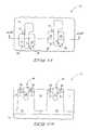
- FIG. 1is a diagrammatic top plan view of a semiconductor substrate in process in accordance with an aspect of the invention.
- FIG. 3is a view of the FIG. 1 substrate at a processing subsequent to that depicted by FIG. 1 .
- FIG. 4is a view of the FIG. 3 substrate taken through line 4 - 4 in FIG. 3 .
- FIG. 5is a view of the FIG. 3 substrate at a processing subsequent to that depicted by FIG. 3 .
- FIG. 6is a view of the FIG. 5 substrate taken through line 6 - 6 in FIG. 5 .
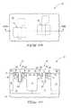
- FIG. 7is a view of the FIG. 5 substrate at a processing subsequent to that depicted by FIG. 5 .
- FIG. 8is a view of the FIG. 7 substrate taken through line 8 - 8 in FIG. 7 .
- FIG. 9is a view of the FIG. 7 substrate at a processing subsequent to that depicted by FIG. 7 .
- FIG. 10is a view of the FIG. 9 substrate taken through line 10 - 10 in FIG. 9 .
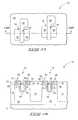
- FIG. 11is a view of the FIG. 9 substrate at a processing subsequent to that depicted by FIG. 9 .
- FIG. 12is a view of the FIG. 11 substrate taken through line 12 - 12 in FIG. 11 .
- FIG. 13is a view of the FIG. 11 substrate at a processing subsequent to that depicted by FIG. 11 .
- FIG. 14is a view of the FIG. 13 substrate taken through line 14 - 14 in FIG. 13 .
- FIG. 15is a view of the FIG. 13 substrate at a processing subsequent to that depicted by FIG. 13 .
- FIG. 17is a view of the FIG. 15 substrate at a processing subsequent to that depicted by FIG. 15 .
- FIG. 18is a view of the FIG. 17 substrate taken through line 18 - 18 in FIG. 17 .
- FIG. 19is a view of the FIG. 17 substrate at a processing subsequent to that depicted by FIG. 17 .
- FIG. 20is a view of the FIG. 19 substrate taken through line 20 - 20 in FIG. 19 .
- Exemplary preferred methods of forming a field effect transistor on a substrateare described with reference to FIGS. 1-20 .
- the field effect transistormight be p-type or n-type.
- the field effect transistorwill comprise a pair of conductively doped source/drain regions, a channel region received intermediate the pair of source/drain regions, and a transistor gate received operably proximate the channel region.
- An exemplary preferred embodiment methodis described in forming both an n-channel field effect transistor and a p-channel field effect transistor on a substrate, although methods in accordance with the invention might be utilized to fabricate only a single conductivity type field effect transistor.
- an exemplary substrate fragment in processis indicated generally with reference numeral 10 .
- Suchpreferably comprises a semiconductive substrate, with the depicted preferred example comprising bulk monocrystalline semiconductive material 12 (for example, silicon), although other substrates (for example, semiconductor-on-insulator substrates) are also contemplated.
- semiconductor substrateor “semiconductive substrate” is defined to mean any construction comprising semiconductive material, including, but not limited to, bulk semiconductive materials such as a semiconductive wafer (either alone or in assemblies comprising other materials thereon), and semiconductive material layers (either alone or in assemblies comprising other materials).
- substraterefers to any supporting structure, including, but not limited to, the semiconductive substrates described above.
- Trench isolation material 14has been formed relative to substrate 12 , for example comprising one or a combination of silicon dioxide and silicon nitride.
- semiconductive material 12has been suitably background doped with p-type material (i.e., boron) to define a p-well 20 having a suitable dopant concentration to function as an NMOS channel.
- Trench isolation regions 14have been fabricated to define an exemplary substrate area 16 in which an n-channel field effect transistor will be fabricated, and an area 18 in which a p-channel field effect transistor will be fabricated.
- n-channel region/area 16has been suitably masked, for example with a photoresist layer 22 .
- Suitable background n-type dopinghas occurred to form an n-well region 24 within p-channel region/area 18 .
- p-type conductivity enhancing impurity dopanthas been ion implanted into a first region 26 of semiconductive material 24 of the substrate to a highest dopant concentration for the pair of source/drain regions of the p-channel field effect transistor being fabricated.
- An exemplary implant materialis boron, for example deposited to an exemplary dopant concentration of from 1 ⁇ 10 13 ions/cm 3 to 1 ⁇ 10 16 ions/cm 3 .
- An exemplary thickness of implanted first region 26is from 300 Angstroms to 500 Angstroms, with an exemplary depth for peak implant concentration being from 200 Angstroms to 400 Angstroms.
- first region 26A conductivity enhancing impurity might be provided within first region 26 by any existing or yet-to-be developed manner, including those other than ion implanting, for example by gas phase diffusion.
- first region 26will be fabricated to comprise a pair of source/drain regions 28 of the p-channel field effect transistor being fabricated, with region 26 constituting the highest dopant concentration portions thereof and as will become apparent from the continuing discussion. Accordingly, separate portions of first region 26 will constitute the highest dopant concentration portions of source/drain regions 28 .
- aspects of the inventioncontemplate ion implanting a conductivity modifying impurity dopant into semiconductive material 24 of the substrate to form at least one lower dopant concentration portion 30 received proximate each highest dopant concentration portion of region 26 of each source/drain region 28 .
- lower dopant concentration portion 30is depicted as being received below first region 26 .
- such regionmight comprise one or a combination of a threshold voltage (V t ) adjust implant and a lightly doped drain (LDD) implant.
- V tthreshold voltage
- LDDlightly doped drain
- An example dopant materialcomprises arsenic, for example implanted to concentration of from 1 ⁇ 10 12 ions/cm 3 to 1 ⁇ 10 13 ions/cm 3 .
- the lower dopant concentration portions formed proximate each highest dopant concentration portion of the field effect transistormight be of the same conductivity type as the highest dopant concentration portion, or of different conductivity types. Further if of the same conductivity type, the dopant of the lower dopant concentration portions and the dopant of the highest dopant concentration portions might be of the same or different compositions.
- p-channel region/area 18has been masked, for example with photoresist 32 , and an n-type conductivity enhancing impurity dopant has been ion implanted into a second region 34 of semiconductive material 20 of the substrate to a highest dopant concentration for the pair of source/drain regions of the n-channel field effect transistor being fabricated.
- An exemplary dopant concentrationis the same as that described above for first region 26 .
- An exemplary suitable n-type implant materialis arsenic, and exemplary preferred thickness and peak implant depth for second region 34 are the same as those for first region 26 .
- a conductivity enhancing impuritymight be provided within first region 26 by any existing or yet-to-be developed manner, including those other than ion implanting, for example by gas phase diffusion.
- second region 34will be fabricated to comprise a pair of source/drain regions 36 of the n-channel field effect transistor being fabricated, with region 34 constituting the highest dopant concentration portions thereof and as will become apparent from the continuing discussion. Accordingly, separate portions of second region 34 will constitute the highest dopant concentration portions of source/drain regions 36 .
- FIGS. 7 and 8also depict exemplary preferred ion implanting of a conductivity modifying impurity dopant into the semiconductive material of the substrate to form at least one lower dopant concentration portion 38 proximate each highest dopant concentration portion of region 34 of source/drain regions 36 being fabricated.
- a preferred orientation for implant region 38is lower in the semiconductive material than are the highest dopant concentration portions of region 34 .
- lower dopant concentration portions of region 38might be of the same conductivity type as those of the portions of region 34 , or of different conductivity types. If of the same conductivity type, the dopants might be of the same composition or of different compositions.
- region 38is depicted as comprising a V t adjust implant of opposite conductivity type to that of n+ region 34 .
- An example dopant materialcomprises boron, for example implanted to concentration of from 1 ⁇ 10 12 ions/cm 3 to 1 ⁇ 10 13 ions/cm 3 .
- photoresist mask 32(not shown) has been removed, and the substrate subjected to a dopant activation anneal to simultaneously activate the dopants in regions 16 and 18 .
- a dopant activation annealto simultaneously activate the dopants in regions 16 and 18 .
- Any existing or yet-to-be developed anneal technique effective for dopant activation where requiredis contemplated.
- one exemplary preferred techniqueincludes exposing the substrate to rapid thermal processing (RTP) at a temperature of at least 920° C. for from 10 seconds to 90 seconds, or furnace anneal at a temperature of at least 600° C. for from 20 minutes to 60 minutes.
- RTPrapid thermal processing
- a first opening 44has been etched through first region 26 (and also through lower dopant concentration portion 30 received therebeneath) into semiconductive material 24 of the substrate.
- a second opening 46has been etched through second region 34 (and also preferably through lower dopant concentration portion 38 received therebeneath) into semiconductive material 20 of the substrate.
- Suchis preferably conducted simultaneously, for example utilizing one or more common masking and etching steps.
- Suchis also depicted, by way of example only, as forming openings 44 and 46 to extend over and within trench isolation 14 .
- desired field effect transistor gateswill be formed within openings 44 and 46 .
- opening 44is laterally centered relative to implant region 26 in at least one respective straight line cross-section of the substrate, for example the cross-section line 12 - 12 as shown in FIG. 11 .
- opening 46is laterally centered relative to implant region 34 in at least one respective straight line cross-section of the substrate, for example the cross-section line 12 - 12 as shown in FIG. 11 .
- FIGS. 13 and 14depict forming a suitable gate dielectric 50 within first opening 44 and second opening 46 .
- a suitable gate dielectric 50might comprise the same or different one or more materials for the respective transistors being fabricated, with examples including one or a combination of silicon dioxide, silicon nitride, aluminum oxide, hafnium oxide and zirconium oxide, and other preferred high-k dielectric materials.
- different gate dielectric thicknesscan be provided if desired for the different p-channel and n-channel devices.
- conductive material 54 of the transistor gate of the p-channel field effect transistorhas been formed over gate dielectric 50 within first opening 44 and conductive material 54 of the transistor gate of the n-channel field effect transistor has been formed over gate dielectric 50 within second opening 46 .
- the conductive material of the transistor gate of the p-channel field effect transistor and the conductive material of the transistor gate of the n-channel field effect transistormight be of the same or different compositions. Ideally, such are typically of at least slightly modified compositions for obtaining different and desired work functions for the respective p-channel and n-channel devices. Accordingly in such processing, separate depositions might occur relative to the material deposited to within openings 44 and 46 , or a commonly deposited material 54 subjected to separate masked processings of such material within the respective openings 44 and 46 .
- Exemplary preferred conductive material from which conductive portions of the transistor gates are madeinclude elemental-form metal (including alloys thereof), conductive metal compounds, and less preferably conductively doped semiconductive material (i.e., conductively doped polysilicon).
- Exemplary preferred materialsinclude TaSiN for n-channel devices and TiN for p-channel devices. However of course, other elemental metals and metal compounds are contemplated.
- FIGS. 15 and 16depict the formation of conductive material 54 as comprising a deposition which overfills openings 44 and 46 .
- FIGS. 17 and 18depict a preferred-embodiment subsequent removing of some of such deposited conductive material effective to recess material 54 to within openings 44 and 46 .
- Suchthereby forms an n-channel gate 60 and a p-channel gate 62 .
- Each source/drain region 28 for the p-channel field effect transistoris comprised of an exemplary highest dopant concentration portion 26 and at least one lower dopant concentration portion 30 , in the exemplary preferred embodiment.
- each source/drain region 36 of the n-channel field effect transistoris comprised of a highest dopant concentration portion 34 and at least one lower dopant concentration portion 38 .
- an insulative layer 70for example silicon nitride
- An exemplary thickness range for layer 70is from 50 Angstroms to 200 Angstroms.
- a thicker, different composition, insulative material layer 71i.e., silicon dioxide deposited by the decomposition of tetraethylorthosilicate
- An exemplary thickness range for layer 71is from 1,000 Angstroms to 10,000 Angstroms.
- Contact openings 72have been fabricated into and through layers 71 and 70 to provide the desired exposure to the respective source/drain regions and conductive material extending from the transistor gates. Suitable conductive contacts (not shown) would be formed thereto for the effective connection of such components with other conductive interconnects or devices (i.e., capacitors and/or conductive interconnect lines).
- first region 26depicts the semiconductive material of first region 26 , the semiconductive material of second region 34 , and the semiconductive material beneath such regions into which first opening 44 and into which second opening 46 are etched to each comprise bulk monocrystalline semiconductive material, for example bulk monocrystalline silicon.
- semiconductive materialas comprising other than bulk monocrystalline material, for example semiconductor-on-insulator substrates and material, and other substrates whether existing or yet-to-be developed.
- Such exemplary preferred embodimentsalso depict the fabrication of the field effect transistor gate within an opening or trench formed within a semiconductor substrate such as bulk monocrystalline semiconductor material.
- the inventionis in no way so limited. Aspects of the invention contemplate conducting a dopant activation anneal of a pair of source/drain regions prior to depositing material from which a conductive portion of the transistor gate is made regardless of the substrate or transistor orientation/structure.
- the field effect transistor gatecould be formed outwardly of a bulk monocrystalline semiconductive material substrate, for example with respect to a conventional or yet-to-be developed horizontal/planar transistor, and wherein the pair of source/drain regions where subjected to a dopant activation anneal prior to the fabrication of a conductive portion of a transistor gate received operably between the source/drain regions over a channel region formed therebetween.
- the inventioncontemplates conducting a dopant activation anneal of a pair of elevated source/drain regions of a horizontally-oriented field effect transistor, and for example regardless of whether such elevated source/drain regions are formed on or over bulk monocrystalline semiconductive material.
Landscapes
- Physics & Mathematics (AREA)
- Engineering & Computer Science (AREA)
- High Energy & Nuclear Physics (AREA)
- General Physics & Mathematics (AREA)
- Toxicology (AREA)
- Condensed Matter Physics & Semiconductors (AREA)
- Health & Medical Sciences (AREA)
- Manufacturing & Machinery (AREA)
- Computer Hardware Design (AREA)
- Microelectronics & Electronic Packaging (AREA)
- Power Engineering (AREA)
- Insulated Gate Type Field-Effect Transistor (AREA)
- Metal-Oxide And Bipolar Metal-Oxide Semiconductor Integrated Circuits (AREA)
Abstract
Description
Claims (25)
Priority Applications (2)
| Application Number | Priority Date | Filing Date | Title |
|---|---|---|---|
| US12/969,418US8426273B2 (en) | 2005-08-30 | 2010-12-15 | Methods of forming field effect transistors on substrates |
| US13/865,117US8877589B2 (en) | 2005-08-30 | 2013-04-17 | Methods of forming field effect transistors on substrates |
Applications Claiming Priority (2)
| Application Number | Priority Date | Filing Date | Title |
|---|---|---|---|
| US11/215,477US7867851B2 (en) | 2005-08-30 | 2005-08-30 | Methods of forming field effect transistors on substrates |
| US12/969,418US8426273B2 (en) | 2005-08-30 | 2010-12-15 | Methods of forming field effect transistors on substrates |
Related Parent Applications (1)
| Application Number | Title | Priority Date | Filing Date |
|---|---|---|---|
| US11/215,477DivisionUS7867851B2 (en) | 2005-08-30 | 2005-08-30 | Methods of forming field effect transistors on substrates |
Related Child Applications (1)
| Application Number | Title | Priority Date | Filing Date |
|---|---|---|---|
| US13/865,117ContinuationUS8877589B2 (en) | 2005-08-30 | 2013-04-17 | Methods of forming field effect transistors on substrates |
Publications (2)
| Publication Number | Publication Date |
|---|---|
| US20110086476A1 US20110086476A1 (en) | 2011-04-14 |
| US8426273B2true US8426273B2 (en) | 2013-04-23 |
Family
ID=37307486
Family Applications (3)
| Application Number | Title | Priority Date | Filing Date |
|---|---|---|---|
| US11/215,477Expired - Fee RelatedUS7867851B2 (en) | 2005-08-30 | 2005-08-30 | Methods of forming field effect transistors on substrates |
| US12/969,418Expired - LifetimeUS8426273B2 (en) | 2005-08-30 | 2010-12-15 | Methods of forming field effect transistors on substrates |
| US13/865,117Expired - LifetimeUS8877589B2 (en) | 2005-08-30 | 2013-04-17 | Methods of forming field effect transistors on substrates |
Family Applications Before (1)
| Application Number | Title | Priority Date | Filing Date |
|---|---|---|---|
| US11/215,477Expired - Fee RelatedUS7867851B2 (en) | 2005-08-30 | 2005-08-30 | Methods of forming field effect transistors on substrates |
Family Applications After (1)
| Application Number | Title | Priority Date | Filing Date |
|---|---|---|---|
| US13/865,117Expired - LifetimeUS8877589B2 (en) | 2005-08-30 | 2013-04-17 | Methods of forming field effect transistors on substrates |
Country Status (3)
| Country | Link |
|---|---|
| US (3) | US7867851B2 (en) |
| TW (1) | TWI368262B (en) |
| WO (1) | WO2007027416A1 (en) |
Cited By (3)
| Publication number | Priority date | Publication date | Assignee | Title |
|---|---|---|---|---|
| US20130230957A1 (en)* | 2005-08-30 | 2013-09-05 | Micron Technology, Inc. | Methods of Forming Field Effect Transistors on Substrates |
| US8916912B2 (en) | 2005-07-08 | 2014-12-23 | Micron Technology, Inc. | Semiconductor device comprising a transistor gate having multiple vertically oriented sidewalls |
| US11088264B2 (en) | 2015-06-11 | 2021-08-10 | International Business Machines Corporation | Self-aligned channel-only semiconductor-on-insulator field effect transistor |
Families Citing this family (27)
| Publication number | Priority date | Publication date | Assignee | Title |
|---|---|---|---|---|
| US7547945B2 (en)* | 2004-09-01 | 2009-06-16 | Micron Technology, Inc. | Transistor devices, transistor structures and semiconductor constructions |
| US7384849B2 (en) | 2005-03-25 | 2008-06-10 | Micron Technology, Inc. | Methods of forming recessed access devices associated with semiconductor constructions |
| JP2007194562A (en)* | 2006-01-23 | 2007-08-02 | Nec Electronics Corp | Semiconductor device and manufacturing method thereof |
| US7700441B2 (en)* | 2006-02-02 | 2010-04-20 | Micron Technology, Inc. | Methods of forming field effect transistors, methods of forming field effect transistor gates, methods of forming integrated circuitry comprising a transistor gate array and circuitry peripheral to the gate array, and methods of forming integrated circuitry comprising a transistor gate array including first gates and second grounded isolation gates |
| US20070262395A1 (en) | 2006-05-11 | 2007-11-15 | Gibbons Jasper S | Memory cell access devices and methods of making the same |
| US8008144B2 (en) | 2006-05-11 | 2011-08-30 | Micron Technology, Inc. | Dual work function recessed access device and methods of forming |
| US8860174B2 (en)* | 2006-05-11 | 2014-10-14 | Micron Technology, Inc. | Recessed antifuse structures and methods of making the same |
| KR100780656B1 (en)* | 2006-06-29 | 2007-11-29 | 주식회사 하이닉스반도체 | Method of manufacturing recess gate of semiconductor device |
| US7602001B2 (en) | 2006-07-17 | 2009-10-13 | Micron Technology, Inc. | Capacitorless one transistor DRAM cell, integrated circuitry comprising an array of capacitorless one transistor DRAM cells, and method of forming lines of capacitorless one transistor DRAM cells |
| US7772632B2 (en)* | 2006-08-21 | 2010-08-10 | Micron Technology, Inc. | Memory arrays and methods of fabricating memory arrays |
| US7589995B2 (en)* | 2006-09-07 | 2009-09-15 | Micron Technology, Inc. | One-transistor memory cell with bias gate |
| US20080296674A1 (en)* | 2007-05-30 | 2008-12-04 | Qimonda Ag | Transistor, integrated circuit and method of forming an integrated circuit |
| US7923373B2 (en) | 2007-06-04 | 2011-04-12 | Micron Technology, Inc. | Pitch multiplication using self-assembling materials |
| KR101535222B1 (en)* | 2008-04-17 | 2015-07-08 | 삼성전자주식회사 | Semiconductor device and method of fabricating the same |
| CN101621029B (en)* | 2008-07-03 | 2011-01-12 | 中芯国际集成电路制造(上海)有限公司 | DRAM cell structure with selective anti-narrow width effect and generation method thereof |
| US8193579B2 (en)* | 2008-07-29 | 2012-06-05 | Rohm Co., Ltd. | Trench type semiconductor device and fabrication method for the same |
| US8692310B2 (en) | 2009-02-09 | 2014-04-08 | Spansion Llc | Gate fringing effect based channel formation for semiconductor device |
| KR101602446B1 (en)* | 2009-02-12 | 2016-03-15 | 삼성전자주식회사 | Method of fabricating a semiconductor device having a threshold voltage control region |
| KR101094372B1 (en)* | 2009-06-30 | 2011-12-15 | 주식회사 하이닉스반도체 | Method of manufacturing semiconductor device with buried gate |
| KR20120126433A (en)* | 2011-05-11 | 2012-11-21 | 에스케이하이닉스 주식회사 | Semiconductor device and manufacturing method of the same |
| US9059142B2 (en)* | 2012-07-23 | 2015-06-16 | Nanya Technology Corporation | Semiconductor device having vertical gates and fabrication thereof |
| TWI497649B (en)* | 2013-04-01 | 2015-08-21 | Inotera Memories Inc | Buried word line structure and manufacturing method thereof |
| US9472542B2 (en)* | 2013-09-11 | 2016-10-18 | Micron Technology, Inc. | DRAM arrays, semiconductor constructions and DRAM array layouts |
| US9640656B2 (en)* | 2014-04-04 | 2017-05-02 | Micron Technology, Inc. | Transistors having strained channel under gate in a recess |
| KR102707534B1 (en) | 2016-12-02 | 2024-09-20 | 삼성전자주식회사 | Semiconductor memory device |
| CN110911407B (en)* | 2018-09-18 | 2025-03-28 | 长鑫存储技术有限公司 | Semiconductor device and method for forming the same |
| US11189623B2 (en) | 2018-12-18 | 2021-11-30 | Micron Technology, Inc. | Apparatuses, memory devices, and electronic systems |
Citations (291)
| Publication number | Priority date | Publication date | Assignee | Title |
|---|---|---|---|---|
| US4455740A (en) | 1979-12-07 | 1984-06-26 | Tokyo Shibaura Denki Kabushiki Kaisha | Method of manufacturing a self-aligned U-MOS semiconductor device |
| US4722910A (en) | 1986-05-27 | 1988-02-02 | Analog Devices, Inc. | Partially self-aligned metal contact process |
| US4835741A (en) | 1986-06-02 | 1989-05-30 | Texas Instruments Incorporated | Frasable electrically programmable read only memory cell using a three dimensional trench floating gate |
| US4922460A (en) | 1987-01-26 | 1990-05-01 | Mitsubishi Denki Kabushiki Kaisha | Semiconductor memory device with folded bit line structure suitable for high density |
| US4931409A (en) | 1988-01-30 | 1990-06-05 | Kabushiki Kaisha Toshiba | Method of manufacturing semiconductor device having trench isolation |
| US4937641A (en) | 1983-09-28 | 1990-06-26 | Hitachi, Ltd. | Semiconductor memory and method of producing the same |
| US4939793A (en) | 1986-04-17 | 1990-07-03 | Plessey Overseas Limited | Integrated circuit assembly with optically coupled components |
| US4939100A (en) | 1987-12-18 | 1990-07-03 | Commissariat A L'energie Atomique | Process for the production of a MIS transistor with a raised substrate/gate dielectric interface end |
| US4979004A (en) | 1988-01-29 | 1990-12-18 | Texas Instruments Incorporated | Floating gate memory cell and device |
| US5014110A (en) | 1988-06-03 | 1991-05-07 | Mitsubishi Denki Kabushiki Kaisha | Wiring structures for semiconductor memory device |
| US5013680A (en) | 1990-07-18 | 1991-05-07 | Micron Technology, Inc. | Process for fabricating a DRAM array having feature widths that transcend the resolution limit of available photolithography |
| US5021355A (en) | 1989-05-22 | 1991-06-04 | International Business Machines Corporation | Method of fabricating cross-point lightly-doped drain-source trench transistor |
| US5047117A (en) | 1990-09-26 | 1991-09-10 | Micron Technology, Inc. | Method of forming a narrow self-aligned, annular opening in a masking layer |
| US5107459A (en) | 1990-04-20 | 1992-04-21 | International Business Machines Corporation | Stacked bit-line architecture for high density cross-point memory cell array |
| US5108938A (en) | 1989-03-21 | 1992-04-28 | Grumman Aerospace Corporation | Method of making a trench gate complimentary metal oxide semiconductor transistor |
| US5122848A (en) | 1991-04-08 | 1992-06-16 | Micron Technology, Inc. | Insulated-gate vertical field-effect transistor with high current drive and minimum overlap capacitance |
| US5160491A (en) | 1986-10-21 | 1992-11-03 | Texas Instruments Incorporated | Method of making a vertical MOS transistor |
| US5244824A (en) | 1990-09-05 | 1993-09-14 | Motorola, Inc. | Trench capacitor and transistor structure and method for making the same |
| US5254218A (en) | 1992-04-22 | 1993-10-19 | Micron Technology, Inc. | Masking layer having narrow isolated spacings and the method for forming said masking layer and the method for forming narrow isolated trenches defined by said masking layer |
| US5281548A (en) | 1992-07-28 | 1994-01-25 | Micron Technology, Inc. | Plug-based floating gate memory |
| US5358879A (en) | 1993-04-30 | 1994-10-25 | Loral Federal Systems Company | Method of making gate overlapped lightly doped drain for buried channel devices |
| US5371024A (en) | 1988-09-30 | 1994-12-06 | Kabushiki Kaisha Toshiba | Semiconductor device and process for manufacturing the same |
| US5376575A (en) | 1991-09-26 | 1994-12-27 | Hyundai Electronics Industries, Inc. | Method of making dynamic random access memory having a vertical transistor |
| US5392237A (en) | 1992-09-25 | 1995-02-21 | Rohm Co., Ltd. | Semiconductor memory device with EEPROM in trench with polysilicon/metal contacting to source and drain in virtual ground type array |
| US5413949A (en) | 1994-04-26 | 1995-05-09 | United Microelectronics Corporation | Method of making self-aligned MOSFET |
| US5446299A (en) | 1994-04-29 | 1995-08-29 | International Business Machines Corporation | Semiconductor random access memory cell on silicon-on-insulator with dual control gates |
| US5467305A (en) | 1992-03-12 | 1995-11-14 | International Business Machines Corporation | Three-dimensional direct-write EEPROM arrays and fabrication methods |
| US5480838A (en) | 1992-07-03 | 1996-01-02 | Mitsubishi Denki Kabushiki Kaisha | Method of manufacturing a semiconductor device having vertical transistor with tubular double-gate |
| US5496751A (en)* | 1993-05-07 | 1996-03-05 | Vlsi Technology, Inc. | Method of forming an ESD and hot carrier resistant integrated circuit structure |
| US5502320A (en) | 1993-03-15 | 1996-03-26 | Kabushiki Kaisha Toshiba | Dynamic random access memory (DRAM) semiconductor device |
| US5514604A (en)* | 1993-12-08 | 1996-05-07 | General Electric Company | Vertical channel silicon carbide metal-oxide-semiconductor field effect transistor with self-aligned gate for microwave and power applications, and method of making |
| US5532089A (en) | 1993-12-23 | 1996-07-02 | International Business Machines Corporation | Simplified fabrication methods for rim phase-shift masks |
| US5567634A (en) | 1995-05-01 | 1996-10-22 | National Semiconductor Corporation | Method of fabricating self-aligned contact trench DMOS transistors |
| US5574621A (en) | 1995-03-27 | 1996-11-12 | Motorola, Inc. | Integrated circuit capacitor having a conductive trench |
| US5573837A (en) | 1992-04-22 | 1996-11-12 | Micron Technology, Inc. | Masking layer having narrow isolated spacings and the method for forming said masking layer and the method for forming narrow isolated trenches defined by said masking layer |
| US5612559A (en) | 1993-11-24 | 1997-03-18 | Samsung Electronics Co., Ltd. | Semiconductor device having pillar shaped transistor and a method for manufacturing the same |
| US5619057A (en) | 1994-01-19 | 1997-04-08 | Sony Corporation | Complex film overlying a substrate with defined work function |
| EP0453998B1 (en) | 1990-04-21 | 1997-07-02 | Kabushiki Kaisha Toshiba | Semiconductor memory device having a bit line constituted by a semiconductor layer |
| US5687119A (en) | 1995-10-05 | 1997-11-11 | Lg Semicon Co., Ltd. | Semiconductor memory device with floating gate electrode |
| US5693549A (en) | 1994-09-13 | 1997-12-02 | Lg Semicon Co., Ltd. | Method of fabricating thin film transistor with supplementary gates |
| US5714786A (en) | 1996-10-31 | 1998-02-03 | Micron Technology, Inc. | Transistors having controlled conductive spacers, uses of such transistors and methods of making such transistors |
| US5714412A (en) | 1996-12-02 | 1998-02-03 | Taiwan Semiconductor Manufacturing Company, Ltd | Multi-level, split-gate, flash memory cell and method of manufacture thereof |
| US5739066A (en) | 1996-09-17 | 1998-04-14 | Micron Technology, Inc. | Semiconductor processing methods of forming a conductive gate and line |
| US5753947A (en) | 1995-01-20 | 1998-05-19 | Micron Technology, Inc. | Very high-density DRAM cell structure and method for fabricating it |
| US5763305A (en) | 1996-08-16 | 1998-06-09 | United Microelectronics Corporation | Method for forming a semiconductor memory device with a capacitor |
| US5792690A (en) | 1997-05-15 | 1998-08-11 | Vanguard International Semiconductor Corporation | Method of fabricating a DRAM cell with an area equal to four times the used minimum feature |
| US5792687A (en) | 1996-08-01 | 1998-08-11 | Vanguard International Semiconductor Corporation | Method for fabricating high density integrated circuits using oxide and polysilicon spacers |
| US5798544A (en) | 1994-04-22 | 1998-08-25 | Nec Corporation | Semiconductor memory device having trench isolation regions and bit lines formed thereover |
| US5817552A (en) | 1995-05-24 | 1998-10-06 | Siemens Aktiengesellschaft | Process of making a dram cell arrangement |
| US5841611A (en) | 1994-05-02 | 1998-11-24 | Matsushita Electric Industrial Co., Ltd. | Magnetoresistance effect device and magnetoresistance effect type head, memory device, and amplifying device using the same |
| US5869359A (en) | 1997-08-20 | 1999-02-09 | Prabhakar; Venkatraman | Process for forming silicon on insulator devices having elevated source and drain regions |
| US5869382A (en) | 1996-07-02 | 1999-02-09 | Sony Corporation | Structure of capacitor for dynamic random access memory and method of manufacturing thereof |
| US5909618A (en) | 1997-07-08 | 1999-06-01 | Micron Technology, Inc. | Method of making memory cell with vertical transistor and buried word and body lines |
| US5963469A (en) | 1998-02-24 | 1999-10-05 | Micron Technology, Inc. | Vertical bipolar read access for low voltage memory cell |
| US5964750A (en) | 1994-03-15 | 1999-10-12 | Medolas Gesellschaft Fuer Medizintechnik Gmbh | Laser catheter for bypass surgery |
| US5972754A (en) | 1998-06-10 | 1999-10-26 | Mosel Vitelic, Inc. | Method for fabricating MOSFET having increased effective gate length |
| US5977579A (en) | 1998-12-03 | 1999-11-02 | Micron Technology, Inc. | Trench dram cell with vertical device and buried word lines |
| US6015990A (en) | 1997-02-27 | 2000-01-18 | Kabushiki Kaisha Toshiba | Semiconductor memory device and method of manufacturing the same |
| US6033963A (en)* | 1999-08-30 | 2000-03-07 | Taiwan Semiconductor Manufacturing Company | Method of forming a metal gate for CMOS devices using a replacement gate process |
| US6037212A (en) | 1996-08-16 | 2000-03-14 | United Microelectronics Corp. | Method of fabricating a semiconductor memory cell having a tree-type capacitor |
| US6054355A (en)* | 1997-06-30 | 2000-04-25 | Kabushiki Kaisha Toshiba | Method of manufacturing a semiconductor device which includes forming a dummy gate |
| US6059553A (en) | 1996-12-17 | 2000-05-09 | Texas Instruments Incorporated | Integrated circuit dielectrics |
| US6063669A (en) | 1996-02-26 | 2000-05-16 | Nec Corporation | Manufacturing method of semiconductor memory device having a trench gate electrode |
| US6072209A (en) | 1997-07-08 | 2000-06-06 | Micro Technology, Inc. | Four F2 folded bit line DRAM cell structure having buried bit and word lines |
| DE19928781C1 (en) | 1999-06-23 | 2000-07-06 | Siemens Ag | DRAM cell array has deep word line trenches for increasing transistor channel length and has no fixed potential word lines separating adjacent memory cells |
| US6090700A (en) | 1996-03-15 | 2000-07-18 | Vanguard International Semiconductor Corporation | Metallization method for forming interconnects in an integrated circuit |
| JP2000208762A (en) | 1999-01-13 | 2000-07-28 | Sony Corp | Insulation gate field effect transistor and its manufacture |
| US6108191A (en) | 1996-05-21 | 2000-08-22 | Siemens Aktiengesellschaft | Multilayer capacitor with high specific capacitance and production process therefor |
| US6114735A (en) | 1999-07-02 | 2000-09-05 | Micron Technology, Inc. | Field effect transistors and method of forming field effect transistors |
| US6120952A (en) | 1998-10-01 | 2000-09-19 | Micron Technology, Inc. | Methods of reducing proximity effects in lithographic processes |
| US6124611A (en) | 1998-10-30 | 2000-09-26 | Sony Corporation | Epitaxial channel vertical MOS transistor |
| US6150687A (en) | 1997-07-08 | 2000-11-21 | Micron Technology, Inc. | Memory cell having a vertical transistor with buried source/drain and dual gates |
| US6168996B1 (en) | 1997-08-28 | 2001-01-02 | Hitachi, Ltd. | Method of fabricating semiconductor device |
| EP1067597A2 (en) | 1999-05-07 | 2001-01-10 | Chartered Semiconductor Manufacturing Pte Ltd. | Transitors with low overlap capacitance |
| JP2001024161A (en) | 1999-04-30 | 2001-01-26 | Sony Corp | Semiconductor memory cell |
| US6184086B1 (en) | 1995-11-20 | 2001-02-06 | Micron Technology Inc. | Method for forming a floating gate semiconductor device having a portion within a recess |
| US6187643B1 (en) | 1999-06-29 | 2001-02-13 | Varian Semiconductor Equipment Associates, Inc. | Simplified semiconductor device manufacturing using low energy high tilt angle and high energy post-gate ion implantation (PoGI) |
| US6191470B1 (en) | 1997-07-08 | 2001-02-20 | Micron Technology, Inc. | Semiconductor-on-insulator memory cell with buried word and body lines |
| TW428308B (en) | 1998-08-28 | 2001-04-01 | Semiconductor Tech Acad Res Ct | Memory structure in ferroelectric nonvolatile memory and readout method therefor |
| EP1089344A2 (en) | 1999-09-29 | 2001-04-04 | Kabushiki Kaisha Toshiba | Insulated gate field effect transistor and method of fabricating the same |
| US6215149B1 (en) | 1998-08-18 | 2001-04-10 | Samsung Electronics Co., Ltd. | Trenched gate semiconductor device |
| US6214670B1 (en) | 1999-07-22 | 2001-04-10 | Taiwan Semiconductor Manufacturing Company | Method for manufacturing short-channel, metal-gate CMOS devices with superior hot carrier performance |
| US6225669B1 (en) | 1998-09-30 | 2001-05-01 | Advanced Micro Devices, Inc. | Non-uniform gate/dielectric field effect transistor |
| US6255165B1 (en) | 1999-10-18 | 2001-07-03 | Advanced Micro Devices, Inc. | Nitride plug to reduce gate edge lifting |
| US6259142B1 (en) | 1998-04-07 | 2001-07-10 | Advanced Micro Devices, Inc. | Multiple split gate semiconductor device and fabrication method |
| US6258650B1 (en) | 1995-09-19 | 2001-07-10 | Kabushiki Kaisha Toshiba | Method for manufacturing semiconductor memory device |
| US6274497B1 (en) | 1999-11-25 | 2001-08-14 | Taiwan Semiconductor Manufacturing Co., Ltd. | Copper damascene manufacturing process |
| US20010025973A1 (en) | 2000-01-25 | 2001-10-04 | Satoru Yamada | Semiconductor integrated circuit device and process for manufacturing the same |
| US6300177B1 (en) | 2001-01-25 | 2001-10-09 | Chartered Semiconductor Manufacturing Inc. | Method to form transistors with multiple threshold voltages (VT) using a combination of different work function gate materials |
| US6303518B1 (en) | 1999-09-30 | 2001-10-16 | Novellus Systems, Inc. | Methods to improve chemical vapor deposited fluorosilicate glass (FSG) film adhesion to metal barrier or etch stop/diffusion barrier layers |
| US6306755B1 (en) | 1999-05-14 | 2001-10-23 | Koninklijke Philips Electronics N.V. (Kpenv) | Method for endpoint detection during dry etch of submicron features in a semiconductor device |
| US20010038123A1 (en) | 1999-08-11 | 2001-11-08 | Bin Yu | Transistor with dynamic source/drain extensions |
| US20010044181A1 (en) | 1996-11-06 | 2001-11-22 | Fujitsu Limited | Semiconductor device and method for fabricating the same |
| US6323506B1 (en) | 1999-12-21 | 2001-11-27 | Philips Electronics North America Corporation | Self-aligned silicon carbide LMOSFET |
| US6323528B1 (en) | 1991-03-06 | 2001-11-27 | Semiconductor Energy Laboratory Co,. Ltd. | Semiconductor device |
| US6331461B1 (en) | 1996-11-01 | 2001-12-18 | Micron Technology, Inc. | Semiconductor processing methods of forming devices on a substrate, forming device arrays on a substrate, forming conductive lines on a substrate, and forming capacitor arrays on a substrate, and integrated circuitry |
| US20010052617A1 (en) | 2000-03-01 | 2001-12-20 | Shindengen Electric Manufacturing Co., Ltd | Transistor and method of manufacturing the same |
| US6337497B1 (en) | 1997-05-16 | 2002-01-08 | International Business Machines Corporation | Common source transistor capacitor stack |
| US6340614B1 (en) | 2000-10-03 | 2002-01-22 | Vanguard International Semiconductor Corporation | Method of forming a DRAM cell |
| US6349052B1 (en) | 1999-09-13 | 2002-02-19 | Infineon Technologies Ag | DRAM cell arrangement and method for fabricating it |
| US6348385B1 (en) | 2000-11-30 | 2002-02-19 | Chartered Semiconductor Manufacturing Ltd. | Method for a short channel CMOS transistor with small overlay capacitance using in-situ doped spacers with a low dielectric constant |
| US20020022339A1 (en) | 2000-07-27 | 2002-02-21 | Markus Kirchhoff | Method for forming an insulator having a low dielectric constant on a semiconductor substrate |
| US6362506B1 (en) | 1998-08-26 | 2002-03-26 | Texas Instruments Incorporated | Minimization-feasible word line structure for DRAM cell |
| US6372554B1 (en) | 1998-09-04 | 2002-04-16 | Hitachi, Ltd. | Semiconductor integrated circuit device and method for production of the same |
| US6383879B1 (en) | 1999-12-03 | 2002-05-07 | Agere Systems Guardian Corp. | Semiconductor device having a metal gate with a work function compatible with a semiconductor device |
| US6383861B1 (en) | 1999-02-18 | 2002-05-07 | Micron Technology, Inc. | Method of fabricating a dual gate dielectric |
| US6391726B1 (en) | 1999-03-11 | 2002-05-21 | Micron Technology, Inc. | Method of fabricating integrated circuitry |
| JP2002151654A (en) | 2000-11-10 | 2002-05-24 | Sharp Corp | Dielectric capacitor element and method of manufacturing the same |
| US6399490B1 (en) | 2000-06-29 | 2002-06-04 | International Business Machines Corporation | Highly conformal titanium nitride deposition process for high aspect ratio structures |
| JP2002184958A (en) | 2000-12-14 | 2002-06-28 | Sony Corp | Semiconductor device and manufacturing method thereof |
| US6414356B1 (en) | 1998-03-30 | 2002-07-02 | Micron Technology, Inc. | Circuits and methods for dual-gated transistors |
| US6420786B1 (en) | 1996-02-02 | 2002-07-16 | Micron Technology, Inc. | Conductive spacer in a via |
| US20020127796A1 (en) | 2001-03-12 | 2002-09-12 | Franz Hofmann | Method for producing a cell of a semiconductor memory |
| US20020127798A1 (en) | 2001-03-08 | 2002-09-12 | Kirk Prall | 2F2 memory device system and method |
| US20020130378A1 (en) | 2001-03-15 | 2002-09-19 | Leonard Forbes | Technique to mitigate short channel effects with vertical gate transistor with different gate materials |
| US20020135030A1 (en) | 2001-03-22 | 2002-09-26 | Mitsubishi Denki Kabushiki Kaisha | Semiconductor device and manufacturing method thereof |
| US6459142B1 (en) | 1998-01-14 | 2002-10-01 | Infineon Technologies Ag | Power MOSFET |
| US6458653B1 (en) | 2001-01-05 | 2002-10-01 | Samsung Electronics Co., Ltd. | Method for forming lower electrode of cylinder-shaped capacitor preventing twin bit failure |
| US6459138B2 (en) | 1999-09-02 | 2002-10-01 | Micron Technology, Inc. | Capacitor structures |
| US6458925B1 (en) | 1998-08-03 | 2002-10-01 | University Of Maryland, Baltimore | Peptide antagonists of zonulin and methods for use of the same |
| US20020153579A1 (en) | 2001-04-19 | 2002-10-24 | Nec Corporation | Semiconductor device with thin film having high permittivity and uniform thickness |
| US6473333B1 (en) | 1999-05-14 | 2002-10-29 | Hitachi, Ltd. | Storage circuit with layered structure element |
| US6476444B1 (en) | 1999-03-18 | 2002-11-05 | Hyundai Electronics Industries Co., Ltd. | Semiconductor device and method for fabricating the same |
| US20020163039A1 (en) | 2001-05-04 | 2002-11-07 | Clevenger Lawrence A. | High dielectric constant materials as gate dielectrics (insulators) |
| US6495474B1 (en) | 2000-09-11 | 2002-12-17 | Agere Systems Inc. | Method of fabricating a dielectric layer |
| US20020192911A1 (en) | 2000-08-29 | 2002-12-19 | Parke Stephen A. | Damascene double gated transistors and related manufacturing methods |
| US6498062B2 (en) | 2001-04-27 | 2002-12-24 | Micron Technology, Inc. | DRAM access transistor |
| US6498087B2 (en) | 2000-12-01 | 2002-12-24 | Koninklijke Philips Electronics N.V. | Method of increasing the conductivity of a transparent conductive layer |
| US20030001290A1 (en) | 2001-06-29 | 2003-01-02 | Kabushiki Kaisha Toshiba | Semiconductor memory device and method for manufacturing the same |
| EP1271632A1 (en) | 2001-02-06 | 2003-01-02 | Matsushita Electric Industrial Co., Ltd. | Method of forming insulating film and method of producing semiconductor device |
| US20030042512A1 (en) | 2001-08-30 | 2003-03-06 | Micron Technology, Inc. | Vertical transistor and method of making |
| US6552401B1 (en) | 2000-11-27 | 2003-04-22 | Micron Technology | Use of gate electrode workfunction to improve DRAM refresh |
| US6563183B1 (en) | 2001-12-31 | 2003-05-13 | Advanced Micro Devices, Inc. | Gate array with multiple dielectric properties and method for forming same |
| US20030094651A1 (en) | 2001-11-17 | 2003-05-22 | Hynix Semiconductor Inc. | Transistor in semiconductor devices and method of manufacturing the same |
| US6586808B1 (en) | 2002-06-06 | 2003-07-01 | Advanced Micro Devices, Inc. | Semiconductor device having multi-work function gate electrode and multi-segment gate dielectric |
| US20030161201A1 (en) | 2002-02-26 | 2003-08-28 | Michael Sommer | Semiconductor memory with vertical selection transistor |
| US20030164527A1 (en) | 2002-01-16 | 2003-09-04 | Fuji Electric Co., Ltd. | Semiconductor device and its manufacturing method |
| US20030170955A1 (en) | 2001-07-10 | 2003-09-11 | Takahiro Kawamura | Trench-gate semiconductor device and its manufacturing method |
| US20030170941A1 (en) | 2001-05-23 | 2003-09-11 | International Business Machines Corporation | Method for low topography semiconductor device formation |
| US20030169629A1 (en) | 2000-07-31 | 2003-09-11 | Bernd Goebel | Semiconductor memory cell configuration and a method for producing the configuration |
| US6624032B2 (en) | 1999-06-28 | 2003-09-23 | Intel Corporation | Structure and process flow for fabrication of dual gate floating body integrated MOS transistors |
| US6630720B1 (en) | 2001-12-26 | 2003-10-07 | Advanced Micro Devices, Inc. | Asymmetric semiconductor device having dual work function gate and method of fabrication |
| US6632723B2 (en) | 2001-04-26 | 2003-10-14 | Kabushiki Kaisha Toshiba | Semiconductor device |
| US6632714B2 (en) | 1999-03-08 | 2003-10-14 | Kabushiki Kaisha Toshiba | Method for manufacturing semiconductor memory |
| US6645818B1 (en)* | 2002-11-13 | 2003-11-11 | Chartered Semiconductor Manufacturing Ltd. | Method to fabricate dual-metal gate for N- and P-FETs |
| US6645869B1 (en) | 2002-09-26 | 2003-11-11 | Vanguard International Semiconductor Corporation | Etching back process to improve topographic planarization of a polysilicon layer |
| US6656748B2 (en) | 2002-01-31 | 2003-12-02 | Texas Instruments Incorporated | FeRAM capacitor post stack etch clean/repair |
| US20030234414A1 (en) | 2002-06-21 | 2003-12-25 | Brown Kris K. | Memory cell and method for forming the same |
| US20040009644A1 (en) | 2001-05-30 | 2004-01-15 | Toshiharu Suzuki | Method for manufacturing channel gate type field effect transistor |
| US20040018679A1 (en) | 2001-03-03 | 2004-01-29 | Yu Young Sub | Storage electrode of a semiconductor memory device and method for fabricating the same |
| TW574746B (en) | 2002-12-19 | 2004-02-01 | Taiwan Semiconductor Mfg | Method for manufacturing MOSFET with recessed channel |
| US20040034587A1 (en) | 2002-08-19 | 2004-02-19 | Amberson Matthew Gilbert | System and method for calculating intra-period volatility |
| US6696746B1 (en) | 1998-04-29 | 2004-02-24 | Micron Technology, Inc. | Buried conductors |
| JP2004071935A (en) | 2002-08-08 | 2004-03-04 | Toshiba Corp | Semiconductor device and method of manufacturing semiconductor device |
| US6706600B2 (en) | 2001-09-19 | 2004-03-16 | Oki Electric Industry Co., Ltd. | Method of fabricating a split-gate semiconductor device |
| US20040061148A1 (en) | 2002-03-11 | 2004-04-01 | Monolithic System Technology, Inc. | One-transistor floating-body DRAM cell in bulk CMOS process with electrically isolated charge storage region |
| US6717200B1 (en) | 1998-09-30 | 2004-04-06 | Siemens Aktiengesellschaft | Vertical field effect transistor with internal annular gate and method of production |
| US20040065919A1 (en)* | 2002-10-03 | 2004-04-08 | Wilson Peter H. | Trench gate laterally diffused MOSFET devices and methods for making such devices |
| US6720232B1 (en) | 2003-04-10 | 2004-04-13 | Taiwan Semiconductor Manufacturing Company | Method of fabricating an embedded DRAM for metal-insulator-metal (MIM) capacitor structure |
| US20040070028A1 (en) | 2002-10-15 | 2004-04-15 | Semiconductor Components Industries, Llc | Method of forming a low resistance semiconductor device and structure therefor |
| US6724028B2 (en) | 2001-12-10 | 2004-04-20 | Hans Gude Gudesen | Matrix-addressable array of integrated transistor/memory structures |
| US6727137B2 (en) | 1997-08-22 | 2004-04-27 | Micron Technology, Inc. | Processing methods of forming integrated circuitry memory devices, methods of forming DRAM arrays, and related semiconductor masks |
| US20040092115A1 (en) | 2002-11-07 | 2004-05-13 | Winbond Electronics Corp. | Memory device having isolation trenches with different depths and the method for making the same |
| US6744097B2 (en) | 2001-08-02 | 2004-06-01 | Samsung Electronics Co., Ltd. | EEPROM memory cell and method of forming the same |
| US20040125636A1 (en) | 2001-03-14 | 2004-07-01 | Wlodek Kurjanowicz | Interleaved wordline architecture |
| US6767789B1 (en) | 1998-06-26 | 2004-07-27 | International Business Machines Corporation | Method for interconnection between transfer devices and storage capacitors in memory cells and device formed thereby |
| US20040150070A1 (en) | 2003-02-03 | 2004-08-05 | Nec Electronics Corporation | Semiconductor device and method for manufacturing the same |
| US20040159857A1 (en) | 2003-02-17 | 2004-08-19 | Renesas Technology Corp. | Semiconductor device having vertical transistor |
| US6784112B2 (en) | 2001-04-05 | 2004-08-31 | Matsushita Electric Industrial Co., Ltd. | Method for surface treatment of silicon based substrate |
| US20040184298A1 (en) | 2003-03-17 | 2004-09-23 | Hiroyuki Takahashi | Semiconductor memory device |
| US20040188738A1 (en) | 2002-03-06 | 2004-09-30 | Micron Technology, Inc. | Nanotube semiconductor devices and methods for making the same |
| US20040197995A1 (en) | 2003-04-01 | 2004-10-07 | Lee Yong-Kyu | Method of manufacturing twin-ONO-type SONOS memory using reverse self-alignment process |
| US20040222458A1 (en) | 2003-05-06 | 2004-11-11 | Mosel Vitelic, Inc. | Termination structure for trench DMOS device and method of making the same |
| US6818947B2 (en) | 2002-09-19 | 2004-11-16 | Fairchild Semiconductor Corporation | Buried gate-field termination structure |
| US6818515B1 (en) | 2003-06-23 | 2004-11-16 | Promos Technologies Inc. | Method for fabricating semiconductor device with loop line pattern structure |
| US20040232466A1 (en) | 2001-08-14 | 2004-11-25 | Albert Birner | Memory cell with trench capacitor and vertical select transistor and an annular contact-making region formed between them |
| US6825093B2 (en) | 2001-09-28 | 2004-11-30 | Infineon Technologies Ag | Process window enhancement for deep trench spacer conservation |
| US20040259311A1 (en) | 2003-06-17 | 2004-12-23 | Ji-Young Kim | Method of forming transistor having recess channel in semiconductor memory, and structure thereof |
| US20040266081A1 (en)* | 2003-06-25 | 2004-12-30 | Chang-Woo Oh | Methods of forming field effect transistors including raised source/drain regions |
| US6844591B1 (en) | 2003-09-17 | 2005-01-18 | Micron Technology, Inc. | Method of forming DRAM access transistors |
| US20050017240A1 (en) | 2003-07-22 | 2005-01-27 | Pierre Fazan | Integrated circuit device, and method of fabricating same |
| US6849501B2 (en) | 1999-09-01 | 2005-02-01 | Micron Technology, Inc. | Methods for fabricating an improved floating gate memory cell |
| US6849496B2 (en) | 2000-12-06 | 2005-02-01 | Infineon Technologies Ag | DRAM with vertical transistor and trench capacitor memory cells and method of fabrication |
| US20050042833A1 (en) | 2003-08-20 | 2005-02-24 | Jong-Chul Park | Method of manufacturing integrated circuit device including recessed channel transistor |
| US6864536B2 (en) | 2000-12-20 | 2005-03-08 | Winbond Electronics Corporation | Electrostatic discharge protection circuit |
| US20050063224A1 (en) | 2003-09-24 | 2005-03-24 | Pierre Fazan | Low power programming technique for a floating body memory transistor, memory cell, and memory array |
| US20050066892A1 (en) | 2003-09-30 | 2005-03-31 | Tokyo Electron Limited | Deposition of silicon-containing films from hexachlorodisilane |
| JP2005093808A (en) | 2003-09-18 | 2005-04-07 | Fujio Masuoka | Memory cell unit, nonvolatile semiconductor memory device including the same, and memory cell array driving method |
| TWI231042B (en) | 2002-12-27 | 2005-04-11 | Wintek Corp | Method and device to promote the yield rate and uniformity of AMOLED panel |
| US6888770B2 (en) | 2003-05-09 | 2005-05-03 | Kabushiki Kaisha Toshiba | Semiconductor memory device |
| US6888198B1 (en) | 2001-06-04 | 2005-05-03 | Advanced Micro Devices, Inc. | Straddled gate FDSOI device |
| US20050104156A1 (en) | 2003-11-13 | 2005-05-19 | Texas Instruments Incorporated | Forming a semiconductor structure in manufacturing a semiconductor device using one or more epitaxial growth processes |
| US20050106838A1 (en) | 2003-11-17 | 2005-05-19 | Hoon Lim | Semiconductor devices with a source/drain formed on a recessed portion of an isolation layer and methods of fabricating the same |
| US6897109B2 (en) | 2001-09-11 | 2005-05-24 | Samsung Electronics Co., Ltd. | Methods of manufacturing integrated circuit devices having contact holes using multiple insulating layers |
| JP2005142203A (en) | 2003-11-04 | 2005-06-02 | Elpida Memory Inc | Semiconductor device and manufacturing method thereof |
| US20050124130A1 (en) | 2003-04-30 | 2005-06-09 | Leo Mathew | Semiconductor fabrication process with asymmetrical conductive spacers |
| US20050136616A1 (en) | 2003-12-19 | 2005-06-23 | Young-Sun Cho | Method of fabricating a recess channel array transistor using a mask layer with a high etch selectivity with respect to a silicon substrate |
| JP2005175090A (en) | 2003-12-09 | 2005-06-30 | Toshiba Corp | Semiconductor memory device and manufacturing method thereof |
| TWI235479B (en) | 2002-08-15 | 2005-07-01 | Intel Corp | Hourglass RAM |
| US20050158949A1 (en) | 2003-09-04 | 2005-07-21 | Manning Homer M. | Semiconductor devices |
| US20050167751A1 (en) | 2004-02-02 | 2005-08-04 | Kabushiki Kaisha Toshiba | Semiconductor memory device for storing data as state of majority carriers accumulated in channel body and method of manufacturing the same |
| US6930640B2 (en) | 2003-03-28 | 2005-08-16 | Gemtek Technology Co., Ltd. | Dual frequency band inverted-F antenna |
| US6939763B2 (en) | 2001-05-29 | 2005-09-06 | Infineon Technologies Ag | DRAM cell arrangement with vertical MOS transistors, and method for its fabrication |
| WO2005083770A1 (en) | 2004-03-02 | 2005-09-09 | Tae-Pok Rhee | Semiconductor device of high breakdown voltage and manufacturing method thereof |
| JP2005277430A (en) | 2005-04-13 | 2005-10-06 | Renesas Technology Corp | Semiconductor integrated circuit device and manufacturing method of the same |
| US6969662B2 (en) | 2001-06-18 | 2005-11-29 | Pierre Fazan | Semiconductor device |
| US20050275014A1 (en) | 2003-07-14 | 2005-12-15 | Samsung Electronics Co., Ltd. | Integration method of a semiconductor device having a recessed gate electrode |
| US20050275042A1 (en) | 2004-06-10 | 2005-12-15 | Samsung Electronics Co., Ltd. | Semiconductor device including a field effect transistor and method of forming thereof |
| US6979853B2 (en) | 2002-06-14 | 2005-12-27 | Infineon Technologies Ag | DRAM memory cell and memory cell array with fast read/write access |
| US20050287780A1 (en) | 2003-09-04 | 2005-12-29 | Micron Technology, Inc. | Semiconductor constructions |
| US20060046407A1 (en) | 2004-09-01 | 2006-03-02 | Werner Juengling | DRAM cells with vertical transistors |
| US20060043449A1 (en) | 2004-09-01 | 2006-03-02 | Tang Sanh D | Semiconductor constructions and transistors, and methods of forming semiconductor constructions and transistors |
| US20060046424A1 (en) | 2004-08-24 | 2006-03-02 | Chance Randal W | Methods of forming semiconductor constructions |
| US7022573B2 (en) | 2003-01-17 | 2006-04-04 | Nanya Technology Corporation | Stack gate with tip vertical memory and method for fabricating the same |
| US7027334B2 (en) | 2003-05-09 | 2006-04-11 | Kabushiki Kaisha Toshiba | Semiconductor memory device |
| US7030436B2 (en) | 2002-12-04 | 2006-04-18 | Micron Technology, Inc. | Embedded DRAM gain memory cell having MOS transistor body provided with a bi-polar transistor charge injecting means |
| US20060083058A1 (en) | 2004-10-04 | 2006-04-20 | Kabushiki Kaisha Toshiba | Semiconductor memory and FBC memory cell driving method |
| US7042009B2 (en) | 2004-06-30 | 2006-05-09 | Intel Corporation | High mobility tri-gate devices and methods of fabrication |
| US7049196B2 (en) | 1998-02-24 | 2006-05-23 | Micron Technology, Inc. | Vertical gain cell and array for a dynamic random access memory and method for forming the same |
| US20060113588A1 (en) | 2004-11-29 | 2006-06-01 | Sillicon-Based Technology Corp. | Self-aligned trench-type DMOS transistor structure and its manufacturing methods |
| TW200617957A (en) | 2004-05-05 | 2006-06-01 | Impinj Inc | PFET nonvolatile memory |
| US7064365B2 (en) | 2002-11-11 | 2006-06-20 | Samsung Electronics Co., Ltd. | Ferroelectric capacitors including a seed conductive film |
| US7071043B2 (en) | 2002-08-15 | 2006-07-04 | Micron Technology, Inc. | Methods of forming a field effect transistor having source/drain material over insulative material |
| US20060160294A1 (en) | 2005-01-18 | 2006-07-20 | International Business Machines Corporation | Soi device with body contact self-aligned to gate |
| US7091092B2 (en) | 2000-09-27 | 2006-08-15 | Chartered Semiconductor Manufacturing Ltd. | Process flow for a performance enhanced MOSFET with self-aligned, recessed channel |
| US20060194410A1 (en) | 2005-02-28 | 2006-08-31 | Hiroyuki Sugaya | Semiconductor device with cavity and method of manufacture thereof |
| US20060204898A1 (en) | 2005-02-24 | 2006-09-14 | Martin Gutsche | Process for producing sublithographic structures |
| US20060216894A1 (en) | 2005-03-25 | 2006-09-28 | Parekh Kunal R | Methods of forming recessed access devices associated with semiconductor constructions |
| US20060216922A1 (en) | 2005-03-28 | 2006-09-28 | Tran Luan C | Integrated circuit fabrication |
| US7122449B2 (en) | 2002-06-10 | 2006-10-17 | Amberwave Systems Corporation | Methods of fabricating semiconductor structures having epitaxially grown source and drain elements |
| US7125774B2 (en) | 2003-09-09 | 2006-10-24 | Samsung Electronics Co., Ltd. | Method of manufacturing transistor having recessed channel |
| KR100640616B1 (en) | 2004-12-21 | 2006-11-01 | 삼성전자주식회사 | Field effect transistor structure including a buried gate pattern and a method of manufacturing a semiconductor device comprising the same |
| US7135371B2 (en) | 2002-12-31 | 2006-11-14 | Dongbu Electronics, Co., Ltd. | Methods of fabricating semiconductor devices |
| US20060264001A1 (en) | 2004-08-31 | 2006-11-23 | Luan Tran | Structures with increased photo-alignment margins |
| US7148527B2 (en) | 2002-12-18 | 2006-12-12 | Samsung Electronics Co., Ltd. | Semiconductor devices with enlarged recessed gate electrodes |
| US20070001222A1 (en) | 2005-06-30 | 2007-01-04 | Freescale Semiconductor, Inc. | Single transistor memory cell with reduced recombination rates |
| US7160788B2 (en) | 2004-08-23 | 2007-01-09 | Micron Technology, Inc. | Methods of forming integrated circuits |
| US7179706B2 (en) | 2003-08-29 | 2007-02-20 | Micron Technology, Inc. | Permeable capacitor electrode |
| US20070048941A1 (en) | 2005-09-01 | 2007-03-01 | Micron Technology, Inc. | Transistor gate forming methods and transistor structures |
| US20070048942A1 (en) | 2005-08-30 | 2007-03-01 | Micron Technology, Inc. | Methods of forming field effect transistors on substrates |
| US20070045712A1 (en) | 2005-09-01 | 2007-03-01 | Haller Gordon A | Memory cell layout and process flow |
| US20070051997A1 (en) | 2005-08-31 | 2007-03-08 | Gordon Haller | Semiconductor memory device |
| US7199005B2 (en) | 2005-08-02 | 2007-04-03 | Micron Technology, Inc. | Methods of forming pluralities of capacitors |
| US7202127B2 (en) | 2004-08-27 | 2007-04-10 | Micron Technology, Inc. | Methods of forming a plurality of capacitors |
| US20070096204A1 (en) | 2005-10-28 | 2007-05-03 | Elpida Memory, Inc. | Method for manufacturing semiconductor device |
| US7214621B2 (en) | 2005-05-18 | 2007-05-08 | Micron Technology, Inc. | Methods of forming devices associated with semiconductor constructions |
| US20070117310A1 (en) | 2005-03-15 | 2007-05-24 | Micron Technology, Inc. | Multiple deposition for integration of spacers in pitch multiplication process |
| US20070128856A1 (en) | 2005-03-15 | 2007-06-07 | Micron Technology, Inc. | Pitch reduced patterns relative to photolithography features |
| US20070148984A1 (en) | 2004-09-02 | 2007-06-28 | Micron Technology, Inc. | Method for integrated circuit fabrication using pitch multiplication |
| US20070158719A1 (en) | 2006-01-11 | 2007-07-12 | Promos Technologies Inc. | Dynamic random access memory structure and method for preparing the same |
| US7244659B2 (en) | 2005-03-10 | 2007-07-17 | Micron Technology, Inc. | Integrated circuits and methods of forming a field effect transistor |
| US7250650B2 (en) | 2002-11-21 | 2007-07-31 | Infineon Technologies Ag | Field-effect transistor structure and associated semiconductor memory cell |
| US20070178641A1 (en) | 2006-02-02 | 2007-08-02 | Micron Technology, Inc. | Methods of forming field effect transistors, methods of forming field effect transistor gates, methods of forming integrated circuitry comprising a transistor gate array and circuitry peripheral to the gate array, and methods of forming integrated circuitry comprising a transistor gate array including first gates and second grounded isolation gates |
| US7262089B2 (en) | 2004-03-11 | 2007-08-28 | Micron Technology, Inc. | Methods of forming semiconductor structures |
| US20070238299A1 (en) | 2006-04-07 | 2007-10-11 | Micron Technology, Inc. | Simplified pitch doubling process flow |
| US7282401B2 (en) | 2005-07-08 | 2007-10-16 | Micron Technology, Inc. | Method and apparatus for a self-aligned recessed access device (RAD) transistor gate |
| US7285812B2 (en) | 2004-09-02 | 2007-10-23 | Micron Technology, Inc. | Vertical transistors |
| US20070261016A1 (en) | 2006-04-24 | 2007-11-08 | Sandhu Gurtej S | Masking techniques and templates for dense semiconductor fabrication |
| US20080012056A1 (en) | 2006-07-17 | 2008-01-17 | Micron Technology, Inc. | Capacitorless one transistor dram cell, integrated circuitry comprising an array of capacitorless one transistor dram cells, and method of forming lines of capacitorless one transistor dram cells |
| US20080042179A1 (en) | 2006-08-21 | 2008-02-21 | Micron Technology, Inc. | Memory arrays and methods of fabricating memory arrays |
| US20080061346A1 (en) | 2006-09-07 | 2008-03-13 | Micron Technology, Inc. | One-transistor memory cell with bias gate |
| US7349232B2 (en) | 2006-03-15 | 2008-03-25 | Micron Technology, Inc. | 6F2 DRAM cell design with 3F-pitch folded digitline sense amplifier |
| US7351666B2 (en) | 2006-03-17 | 2008-04-01 | International Business Machines Corporation | Layout and process to contact sub-lithographic structures |
| US7393789B2 (en) | 2005-09-01 | 2008-07-01 | Micron Technology, Inc. | Protective coating for planarization |
| US7396781B2 (en) | 2005-06-09 | 2008-07-08 | Micron Technology, Inc. | Method and apparatus for adjusting feature size and position |
| US7413981B2 (en) | 2005-07-29 | 2008-08-19 | Micron Technology, Inc. | Pitch doubled circuit layout |
| US7429536B2 (en) | 2005-05-23 | 2008-09-30 | Micron Technology, Inc. | Methods for forming arrays of small, closely spaced features |
| US7435536B2 (en) | 2004-09-02 | 2008-10-14 | Micron Technology, Inc. | Method to align mask patterns |
| US20080299774A1 (en) | 2007-06-04 | 2008-12-04 | Micron Technology, Inc. | Pitch multiplication using self-assembling materials |
| US20090035655A1 (en) | 2003-04-03 | 2009-02-05 | Lucile Gambut-Garel | Crosslinkable composition for a battery electrolyte |
| US7488685B2 (en) | 2006-04-25 | 2009-02-10 | Micron Technology, Inc. | Process for improving critical dimension uniformity of integrated circuit arrays |
| US7494870B2 (en) | 2007-01-12 | 2009-02-24 | Sandisk Corporation | Methods of forming NAND memory with virtual channel |
| US7495946B2 (en) | 2006-03-02 | 2009-02-24 | Infineon Technologies Ag | Phase change memory fabricated using self-aligned processing |
| US7495294B2 (en) | 2005-12-21 | 2009-02-24 | Sandisk Corporation | Flash devices with shared word lines |
| US7504686B2 (en) | 2003-06-20 | 2009-03-17 | Sandisk Corporation | Self-aligned non-volatile memory cell |
| US7528440B2 (en) | 2003-03-04 | 2009-05-05 | Micron Technology, Inc. | Vertical gain cell |
| US7535745B2 (en) | 2005-06-20 | 2009-05-19 | Kabushiki Kaisha Toshiba | Ferroelectric memory device and method of manufacturing the same |
| US20090173994A1 (en) | 2008-01-07 | 2009-07-09 | Samsung Electronics Co., Ltd. | Recess gate transistor |
| US7560390B2 (en) | 2005-06-02 | 2009-07-14 | Micron Technology, Inc. | Multiple spacer steps for pitch multiplication |
| US7564087B2 (en) | 2002-08-29 | 2009-07-21 | Micron Technology, Inc. | Merged MOS-bipolar capacitor memory cell |
| US7567452B2 (en) | 2005-12-15 | 2009-07-28 | Samsung Electronics Co., Ltd. | Multi-level dynamic memory device having open bit line structure and method of driving the same |
| US7576389B2 (en) | 2006-06-22 | 2009-08-18 | Elpida Memory, Inc. | Semiconductor device and manufacture method thereof |
| US7608503B2 (en) | 2004-11-22 | 2009-10-27 | Macronix International Co., Ltd. | Side wall active pin memory and manufacturing method |
| US7619311B2 (en) | 2007-02-02 | 2009-11-17 | Macronix International Co., Ltd. | Memory cell device with coplanar electrode surface and method |
| US7684245B2 (en) | 2007-10-30 | 2010-03-23 | Atmel Corporation | Non-volatile memory array architecture with joined word lines |
| US7732275B2 (en) | 2007-03-29 | 2010-06-08 | Sandisk Corporation | Methods of forming NAND flash memory with fixed charge |
| US7736980B2 (en) | 2006-03-02 | 2010-06-15 | Micron Technology, Inc. | Vertical gated access transistor |
| US7755132B2 (en) | 2006-08-16 | 2010-07-13 | Sandisk Corporation | Nonvolatile memories with shaped floating gates |
| US7759193B2 (en) | 2008-07-09 | 2010-07-20 | Micron Technology, Inc. | Methods of forming a plurality of capacitors |
| EP1003219B1 (en) | 1998-11-19 | 2011-12-28 | Qimonda AG | DRAM with stacked capacitor and buried word line |
| US20120009772A1 (en) | 2010-07-09 | 2012-01-12 | Suraj Mathew | Gate Constructions Of Recessed Access Devices And Methods Of Forming Gate Constructions Of Recessed Access Devices |
Family Cites Families (18)
| Publication number | Priority date | Publication date | Assignee | Title |
|---|---|---|---|---|
| JPS51147280U (en) | 1975-05-21 | 1976-11-26 | ||
| JPS58220464A (en) | 1982-06-17 | 1983-12-22 | Fujitsu Ltd | Semiconductor memory device |
| JPH0626251B2 (en)* | 1984-11-27 | 1994-04-06 | アメリカン テレフオン アンド テレグラフ カムパニ− | Groove transistor |
| JPH0414253Y2 (en) | 1987-01-09 | 1992-03-31 | ||
| JPH0778977B2 (en) | 1989-03-02 | 1995-08-23 | 松下電器産業株式会社 | Magnetic disk cartridge |
| JPH03219677A (en) | 1990-01-24 | 1991-09-27 | Fujitsu Ltd | semiconductor equipment |
| JPH07106435B2 (en) | 1991-04-15 | 1995-11-15 | 新日本製鐵株式会社 | Twin roll type continuous casting machine |
| DE19524092C2 (en)* | 1995-07-01 | 1997-08-07 | Hewlett Packard Gmbh | Method and device for compressing and displaying digital data, in particular the heart rate of cardiotocographs |
| DE19620625C1 (en) | 1996-05-22 | 1997-10-23 | Siemens Ag | High packing density DRAM cell array |
| US5998835A (en) | 1998-02-17 | 1999-12-07 | International Business Machines Corporation | High performance MOSFET device with raised source and drain |
| US6187653B1 (en)* | 1999-12-17 | 2001-02-13 | Lucent Technologies, Inc. | Method for attractive bonding of two crystalline substrates |
| US6362508B1 (en)* | 2000-04-03 | 2002-03-26 | Tower Semiconductor Ltd. | Triple layer pre-metal dielectric structure for CMOS memory devices |
| US6686616B1 (en) | 2000-05-10 | 2004-02-03 | Cree, Inc. | Silicon carbide metal-semiconductor field effect transistors |
| US6606597B1 (en) | 2000-09-08 | 2003-08-12 | Microsoft Corporation | Augmented-word language model |
| US20060167741A1 (en) | 2005-01-25 | 2006-07-27 | Cisco Technology, Inc. | System and method for designing a supply chain |
| US7350441B2 (en) | 2005-11-15 | 2008-04-01 | 3M Innovative Properties Company | Cutting tool having variable movement at two simultaneously independent speeds in an x-direction into a work piece for making microstructures |
| JP2008021809A (en)* | 2006-07-12 | 2008-01-31 | Elpida Memory Inc | Semiconductor device, and its manufacturing method |
| US8563229B2 (en)* | 2007-07-31 | 2013-10-22 | Micron Technology, Inc. | Process of semiconductor fabrication with mask overlay on pitch multiplied features and associated structures |
- 2005
- 2005-08-30USUS11/215,477patent/US7867851B2/ennot_activeExpired - Fee Related
- 2006
- 2006-08-10WOPCT/US2006/031555patent/WO2007027416A1/enactiveApplication Filing
- 2006-08-21TWTW095130582Apatent/TWI368262B/enactive
- 2010
- 2010-12-15USUS12/969,418patent/US8426273B2/ennot_activeExpired - Lifetime
- 2013
- 2013-04-17USUS13/865,117patent/US8877589B2/ennot_activeExpired - Lifetime
Patent Citations (360)
| Publication number | Priority date | Publication date | Assignee | Title |
|---|---|---|---|---|
| US4455740A (en) | 1979-12-07 | 1984-06-26 | Tokyo Shibaura Denki Kabushiki Kaisha | Method of manufacturing a self-aligned U-MOS semiconductor device |
| US4937641A (en) | 1983-09-28 | 1990-06-26 | Hitachi, Ltd. | Semiconductor memory and method of producing the same |
| US4939793A (en) | 1986-04-17 | 1990-07-03 | Plessey Overseas Limited | Integrated circuit assembly with optically coupled components |
| US4722910A (en) | 1986-05-27 | 1988-02-02 | Analog Devices, Inc. | Partially self-aligned metal contact process |
| US4835741A (en) | 1986-06-02 | 1989-05-30 | Texas Instruments Incorporated | Frasable electrically programmable read only memory cell using a three dimensional trench floating gate |
| US5160491A (en) | 1986-10-21 | 1992-11-03 | Texas Instruments Incorporated | Method of making a vertical MOS transistor |
| US4922460A (en) | 1987-01-26 | 1990-05-01 | Mitsubishi Denki Kabushiki Kaisha | Semiconductor memory device with folded bit line structure suitable for high density |
| US4939100A (en) | 1987-12-18 | 1990-07-03 | Commissariat A L'energie Atomique | Process for the production of a MIS transistor with a raised substrate/gate dielectric interface end |
| US4979004A (en) | 1988-01-29 | 1990-12-18 | Texas Instruments Incorporated | Floating gate memory cell and device |
| US4931409A (en) | 1988-01-30 | 1990-06-05 | Kabushiki Kaisha Toshiba | Method of manufacturing semiconductor device having trench isolation |
| US5014110A (en) | 1988-06-03 | 1991-05-07 | Mitsubishi Denki Kabushiki Kaisha | Wiring structures for semiconductor memory device |
| US5371024A (en) | 1988-09-30 | 1994-12-06 | Kabushiki Kaisha Toshiba | Semiconductor device and process for manufacturing the same |
| US5108938A (en) | 1989-03-21 | 1992-04-28 | Grumman Aerospace Corporation | Method of making a trench gate complimentary metal oxide semiconductor transistor |
| US5021355A (en) | 1989-05-22 | 1991-06-04 | International Business Machines Corporation | Method of fabricating cross-point lightly-doped drain-source trench transistor |
| US5107459A (en) | 1990-04-20 | 1992-04-21 | International Business Machines Corporation | Stacked bit-line architecture for high density cross-point memory cell array |
| EP0453998B1 (en) | 1990-04-21 | 1997-07-02 | Kabushiki Kaisha Toshiba | Semiconductor memory device having a bit line constituted by a semiconductor layer |
| US5013680A (en) | 1990-07-18 | 1991-05-07 | Micron Technology, Inc. | Process for fabricating a DRAM array having feature widths that transcend the resolution limit of available photolithography |
| US5244824A (en) | 1990-09-05 | 1993-09-14 | Motorola, Inc. | Trench capacitor and transistor structure and method for making the same |
| US5047117A (en) | 1990-09-26 | 1991-09-10 | Micron Technology, Inc. | Method of forming a narrow self-aligned, annular opening in a masking layer |
| US6822261B2 (en) | 1991-03-06 | 2004-11-23 | Semiconductor Energy Laboratory Co., Ltd. | Semiconductor device and method for forming the same |
| US6323528B1 (en) | 1991-03-06 | 2001-11-27 | Semiconductor Energy Laboratory Co,. Ltd. | Semiconductor device |
| US5122848A (en) | 1991-04-08 | 1992-06-16 | Micron Technology, Inc. | Insulated-gate vertical field-effect transistor with high current drive and minimum overlap capacitance |
| US5376575A (en) | 1991-09-26 | 1994-12-27 | Hyundai Electronics Industries, Inc. | Method of making dynamic random access memory having a vertical transistor |
| US5504357A (en) | 1991-09-26 | 1996-04-02 | Hyundai Electronics Industries, Co., Ltd. | Dynamic random access memory having a vertical transistor |
| US5467305A (en) | 1992-03-12 | 1995-11-14 | International Business Machines Corporation | Three-dimensional direct-write EEPROM arrays and fabrication methods |
| US5254218A (en) | 1992-04-22 | 1993-10-19 | Micron Technology, Inc. | Masking layer having narrow isolated spacings and the method for forming said masking layer and the method for forming narrow isolated trenches defined by said masking layer |
| US5573837A (en) | 1992-04-22 | 1996-11-12 | Micron Technology, Inc. | Masking layer having narrow isolated spacings and the method for forming said masking layer and the method for forming narrow isolated trenches defined by said masking layer |
| US5480838A (en) | 1992-07-03 | 1996-01-02 | Mitsubishi Denki Kabushiki Kaisha | Method of manufacturing a semiconductor device having vertical transistor with tubular double-gate |
| US5281548A (en) | 1992-07-28 | 1994-01-25 | Micron Technology, Inc. | Plug-based floating gate memory |
| US5392237A (en) | 1992-09-25 | 1995-02-21 | Rohm Co., Ltd. | Semiconductor memory device with EEPROM in trench with polysilicon/metal contacting to source and drain in virtual ground type array |
| US5472893A (en) | 1992-09-25 | 1995-12-05 | Rohm Co., Ltd. | Method of making a floating gate memory device |
| US5502320A (en) | 1993-03-15 | 1996-03-26 | Kabushiki Kaisha Toshiba | Dynamic random access memory (DRAM) semiconductor device |
| US5358879A (en) | 1993-04-30 | 1994-10-25 | Loral Federal Systems Company | Method of making gate overlapped lightly doped drain for buried channel devices |
| US5496751A (en)* | 1993-05-07 | 1996-03-05 | Vlsi Technology, Inc. | Method of forming an ESD and hot carrier resistant integrated circuit structure |
| US5612559A (en) | 1993-11-24 | 1997-03-18 | Samsung Electronics Co., Ltd. | Semiconductor device having pillar shaped transistor and a method for manufacturing the same |
| US5514604A (en)* | 1993-12-08 | 1996-05-07 | General Electric Company | Vertical channel silicon carbide metal-oxide-semiconductor field effect transistor with self-aligned gate for microwave and power applications, and method of making |
| US5532089A (en) | 1993-12-23 | 1996-07-02 | International Business Machines Corporation | Simplified fabrication methods for rim phase-shift masks |
| US5619057A (en) | 1994-01-19 | 1997-04-08 | Sony Corporation | Complex film overlying a substrate with defined work function |
| US5964750A (en) | 1994-03-15 | 1999-10-12 | Medolas Gesellschaft Fuer Medizintechnik Gmbh | Laser catheter for bypass surgery |
| US5798544A (en) | 1994-04-22 | 1998-08-25 | Nec Corporation | Semiconductor memory device having trench isolation regions and bit lines formed thereover |
| US5512770A (en) | 1994-04-26 | 1996-04-30 | United Microelectronics Corporation | MOSFET device structure three spaced-apart deep boron implanted channel regions aligned with gate electrode of NMOSFET device |
| US5413949A (en) | 1994-04-26 | 1995-05-09 | United Microelectronics Corporation | Method of making self-aligned MOSFET |
| US5446299A (en) | 1994-04-29 | 1995-08-29 | International Business Machines Corporation | Semiconductor random access memory cell on silicon-on-insulator with dual control gates |
| US5841611A (en) | 1994-05-02 | 1998-11-24 | Matsushita Electric Industrial Co., Ltd. | Magnetoresistance effect device and magnetoresistance effect type head, memory device, and amplifying device using the same |
| US5693549A (en) | 1994-09-13 | 1997-12-02 | Lg Semicon Co., Ltd. | Method of fabricating thin film transistor with supplementary gates |
| US6096596A (en) | 1995-01-20 | 2000-08-01 | Micron Technology Inc. | Very high-density DRAM cell structure and method for fabricating it |
| US5753947A (en) | 1995-01-20 | 1998-05-19 | Micron Technology, Inc. | Very high-density DRAM cell structure and method for fabricating it |
| US5574621A (en) | 1995-03-27 | 1996-11-12 | Motorola, Inc. | Integrated circuit capacitor having a conductive trench |
| US5567634A (en) | 1995-05-01 | 1996-10-22 | National Semiconductor Corporation | Method of fabricating self-aligned contact trench DMOS transistors |
| US5817552A (en) | 1995-05-24 | 1998-10-06 | Siemens Aktiengesellschaft | Process of making a dram cell arrangement |
| US6258650B1 (en) | 1995-09-19 | 2001-07-10 | Kabushiki Kaisha Toshiba | Method for manufacturing semiconductor memory device |
| US5687119A (en) | 1995-10-05 | 1997-11-11 | Lg Semicon Co., Ltd. | Semiconductor memory device with floating gate electrode |
| US6184086B1 (en) | 1995-11-20 | 2001-02-06 | Micron Technology Inc. | Method for forming a floating gate semiconductor device having a portion within a recess |
| US6420786B1 (en) | 1996-02-02 | 2002-07-16 | Micron Technology, Inc. | Conductive spacer in a via |
| US6063669A (en) | 1996-02-26 | 2000-05-16 | Nec Corporation | Manufacturing method of semiconductor memory device having a trench gate electrode |
| US6090700A (en) | 1996-03-15 | 2000-07-18 | Vanguard International Semiconductor Corporation | Metallization method for forming interconnects in an integrated circuit |
| US6108191A (en) | 1996-05-21 | 2000-08-22 | Siemens Aktiengesellschaft | Multilayer capacitor with high specific capacitance and production process therefor |
| US5869382A (en) | 1996-07-02 | 1999-02-09 | Sony Corporation | Structure of capacitor for dynamic random access memory and method of manufacturing thereof |
| US5792687A (en) | 1996-08-01 | 1998-08-11 | Vanguard International Semiconductor Corporation | Method for fabricating high density integrated circuits using oxide and polysilicon spacers |
| US5763305A (en) | 1996-08-16 | 1998-06-09 | United Microelectronics Corporation | Method for forming a semiconductor memory device with a capacitor |
| US6037212A (en) | 1996-08-16 | 2000-03-14 | United Microelectronics Corp. | Method of fabricating a semiconductor memory cell having a tree-type capacitor |
| US5739066A (en) | 1996-09-17 | 1998-04-14 | Micron Technology, Inc. | Semiconductor processing methods of forming a conductive gate and line |
| US7005710B1 (en) | 1996-10-31 | 2006-02-28 | Micron Technology, Inc. | Transistors having controlled conductive spacers, uses of such transistors and methods of making such transistors |
| US6005273A (en) | 1996-10-31 | 1999-12-21 | Micron Technology, Inc. | Transistors having controlled conductive spacers, uses of such transistors and methods of making such transistors |
| US5714786A (en) | 1996-10-31 | 1998-02-03 | Micron Technology, Inc. | Transistors having controlled conductive spacers, uses of such transistors and methods of making such transistors |
| US6090693A (en) | 1996-10-31 | 2000-07-18 | Micron Technology, Inc. | Transistors having controlled conductive spacers, uses of such transistors and methods of making such transistors |
| US6331461B1 (en) | 1996-11-01 | 2001-12-18 | Micron Technology, Inc. | Semiconductor processing methods of forming devices on a substrate, forming device arrays on a substrate, forming conductive lines on a substrate, and forming capacitor arrays on a substrate, and integrated circuitry |
| US20010044181A1 (en) | 1996-11-06 | 2001-11-22 | Fujitsu Limited | Semiconductor device and method for fabricating the same |
| US5714412A (en) | 1996-12-02 | 1998-02-03 | Taiwan Semiconductor Manufacturing Company, Ltd | Multi-level, split-gate, flash memory cell and method of manufacture thereof |
| US6059553A (en) | 1996-12-17 | 2000-05-09 | Texas Instruments Incorporated | Integrated circuit dielectrics |
| US6015990A (en) | 1997-02-27 | 2000-01-18 | Kabushiki Kaisha Toshiba | Semiconductor memory device and method of manufacturing the same |
| US5792690A (en) | 1997-05-15 | 1998-08-11 | Vanguard International Semiconductor Corporation | Method of fabricating a DRAM cell with an area equal to four times the used minimum feature |
| US6337497B1 (en) | 1997-05-16 | 2002-01-08 | International Business Machines Corporation | Common source transistor capacitor stack |
| US6054355A (en)* | 1997-06-30 | 2000-04-25 | Kabushiki Kaisha Toshiba | Method of manufacturing a semiconductor device which includes forming a dummy gate |
| US5909618A (en) | 1997-07-08 | 1999-06-01 | Micron Technology, Inc. | Method of making memory cell with vertical transistor and buried word and body lines |
| US6191470B1 (en) | 1997-07-08 | 2001-02-20 | Micron Technology, Inc. | Semiconductor-on-insulator memory cell with buried word and body lines |
| US6818937B2 (en) | 1997-07-08 | 2004-11-16 | Micron Technology, Inc. | Memory cell having a vertical transistor with buried source/drain and dual gates |
| US6150687A (en) | 1997-07-08 | 2000-11-21 | Micron Technology, Inc. | Memory cell having a vertical transistor with buried source/drain and dual gates |
| US6072209A (en) | 1997-07-08 | 2000-06-06 | Micro Technology, Inc. | Four F2 folded bit line DRAM cell structure having buried bit and word lines |
| US5869359A (en) | 1997-08-20 | 1999-02-09 | Prabhakar; Venkatraman | Process for forming silicon on insulator devices having elevated source and drain regions |
| US6727137B2 (en) | 1997-08-22 | 2004-04-27 | Micron Technology, Inc. | Processing methods of forming integrated circuitry memory devices, methods of forming DRAM arrays, and related semiconductor masks |
| US6168996B1 (en) | 1997-08-28 | 2001-01-02 | Hitachi, Ltd. | Method of fabricating semiconductor device |
| US6459142B1 (en) | 1998-01-14 | 2002-10-01 | Infineon Technologies Ag | Power MOSFET |
| US7049196B2 (en) | 1998-02-24 | 2006-05-23 | Micron Technology, Inc. | Vertical gain cell and array for a dynamic random access memory and method for forming the same |
| US5963469A (en) | 1998-02-24 | 1999-10-05 | Micron Technology, Inc. | Vertical bipolar read access for low voltage memory cell |
| US6414356B1 (en) | 1998-03-30 | 2002-07-02 | Micron Technology, Inc. | Circuits and methods for dual-gated transistors |
| US6259142B1 (en) | 1998-04-07 | 2001-07-10 | Advanced Micro Devices, Inc. | Multiple split gate semiconductor device and fabrication method |
| US6696746B1 (en) | 1998-04-29 | 2004-02-24 | Micron Technology, Inc. | Buried conductors |
| US5972754A (en) | 1998-06-10 | 1999-10-26 | Mosel Vitelic, Inc. | Method for fabricating MOSFET having increased effective gate length |
| US6127699A (en) | 1998-06-10 | 2000-10-03 | Mosel Vitelic, Inc. | Method for fabricating MOSFET having increased effective gate length |
| US6767789B1 (en) | 1998-06-26 | 2004-07-27 | International Business Machines Corporation | Method for interconnection between transfer devices and storage capacitors in memory cells and device formed thereby |
| US6458925B1 (en) | 1998-08-03 | 2002-10-01 | University Of Maryland, Baltimore | Peptide antagonists of zonulin and methods for use of the same |
| US6215149B1 (en) | 1998-08-18 | 2001-04-10 | Samsung Electronics Co., Ltd. | Trenched gate semiconductor device |
| US6362506B1 (en) | 1998-08-26 | 2002-03-26 | Texas Instruments Incorporated | Minimization-feasible word line structure for DRAM cell |
| TW428308B (en) | 1998-08-28 | 2001-04-01 | Semiconductor Tech Acad Res Ct | Memory structure in ferroelectric nonvolatile memory and readout method therefor |
| US6372554B1 (en) | 1998-09-04 | 2002-04-16 | Hitachi, Ltd. | Semiconductor integrated circuit device and method for production of the same |
| US6225669B1 (en) | 1998-09-30 | 2001-05-01 | Advanced Micro Devices, Inc. | Non-uniform gate/dielectric field effect transistor |
| US20010017390A1 (en) | 1998-09-30 | 2001-08-30 | Wei Long | Non-uniform gate/dielectric field effect transistor |
| US6717200B1 (en) | 1998-09-30 | 2004-04-06 | Siemens Aktiengesellschaft | Vertical field effect transistor with internal annular gate and method of production |
| US20010002304A1 (en) | 1998-10-01 | 2001-05-31 | Christophe Pierrat | Methods of reducing proximity effects in lithographic processes |
| US6120952A (en) | 1998-10-01 | 2000-09-19 | Micron Technology, Inc. | Methods of reducing proximity effects in lithographic processes |
| EP1125167B1 (en) | 1998-10-01 | 2010-05-12 | Micron Technology, Inc. | Methods of reducing proximity effects in lithographic processes |
| US6319644B2 (en) | 1998-10-01 | 2001-11-20 | Micron Technology, Inc. | Methods of reducing proximity effects in lithographic processes |
| US6284419B2 (en) | 1998-10-01 | 2001-09-04 | Micron Technology, Inc. | Methods of reducing proximity effects in lithographic processes |
| US20010023045A1 (en) | 1998-10-01 | 2001-09-20 | Christophe Pierrat | Methods of reducing proximity effects in lithographic processes |
| US6124611A (en) | 1998-10-30 | 2000-09-26 | Sony Corporation | Epitaxial channel vertical MOS transistor |
| EP1003219B1 (en) | 1998-11-19 | 2011-12-28 | Qimonda AG | DRAM with stacked capacitor and buried word line |
| US5977579A (en) | 1998-12-03 | 1999-11-02 | Micron Technology, Inc. | Trench dram cell with vertical device and buried word lines |
| JP2000208762A (en) | 1999-01-13 | 2000-07-28 | Sony Corp | Insulation gate field effect transistor and its manufacture |
| US6383861B1 (en) | 1999-02-18 | 2002-05-07 | Micron Technology, Inc. | Method of fabricating a dual gate dielectric |
| US6632714B2 (en) | 1999-03-08 | 2003-10-14 | Kabushiki Kaisha Toshiba | Method for manufacturing semiconductor memory |
| US6391726B1 (en) | 1999-03-11 | 2002-05-21 | Micron Technology, Inc. | Method of fabricating integrated circuitry |
| US6476444B1 (en) | 1999-03-18 | 2002-11-05 | Hyundai Electronics Industries Co., Ltd. | Semiconductor device and method for fabricating the same |
| JP2001024161A (en) | 1999-04-30 | 2001-01-26 | Sony Corp | Semiconductor memory cell |
| US6297106B1 (en) | 1999-05-07 | 2001-10-02 | Chartered Semiconductor Manufacturing Ltd. | Transistors with low overlap capacitance |
| EP1067597A2 (en) | 1999-05-07 | 2001-01-10 | Chartered Semiconductor Manufacturing Pte Ltd. | Transitors with low overlap capacitance |
| US6473333B1 (en) | 1999-05-14 | 2002-10-29 | Hitachi, Ltd. | Storage circuit with layered structure element |
| US6306755B1 (en) | 1999-05-14 | 2001-10-23 | Koninklijke Philips Electronics N.V. (Kpenv) | Method for endpoint detection during dry etch of submicron features in a semiconductor device |
| DE19928781C1 (en) | 1999-06-23 | 2000-07-06 | Siemens Ag | DRAM cell array has deep word line trenches for increasing transistor channel length and has no fixed potential word lines separating adjacent memory cells |
| US6624032B2 (en) | 1999-06-28 | 2003-09-23 | Intel Corporation | Structure and process flow for fabrication of dual gate floating body integrated MOS transistors |
| US6187643B1 (en) | 1999-06-29 | 2001-02-13 | Varian Semiconductor Equipment Associates, Inc. | Simplified semiconductor device manufacturing using low energy high tilt angle and high energy post-gate ion implantation (PoGI) |
| US6417085B1 (en) | 1999-07-02 | 2002-07-09 | Micron Technology, Inc. | Methods of forming a field effect transistor gate construction |
| US6114735A (en) | 1999-07-02 | 2000-09-05 | Micron Technology, Inc. | Field effect transistors and method of forming field effect transistors |
| US6214670B1 (en) | 1999-07-22 | 2001-04-10 | Taiwan Semiconductor Manufacturing Company | Method for manufacturing short-channel, metal-gate CMOS devices with superior hot carrier performance |
| US20010038123A1 (en) | 1999-08-11 | 2001-11-08 | Bin Yu | Transistor with dynamic source/drain extensions |
| US6033963A (en)* | 1999-08-30 | 2000-03-07 | Taiwan Semiconductor Manufacturing Company | Method of forming a metal gate for CMOS devices using a replacement gate process |
| US6849501B2 (en) | 1999-09-01 | 2005-02-01 | Micron Technology, Inc. | Methods for fabricating an improved floating gate memory cell |
| US6844230B2 (en) | 1999-09-02 | 2005-01-18 | Micron Technology, Inc. | Methods of forming capacitors and resultant capacitor structures |
| US6459138B2 (en) | 1999-09-02 | 2002-10-01 | Micron Technology, Inc. | Capacitor structures |
| US6349052B1 (en) | 1999-09-13 | 2002-02-19 | Infineon Technologies Ag | DRAM cell arrangement and method for fabricating it |
| EP1089344A2 (en) | 1999-09-29 | 2001-04-04 | Kabushiki Kaisha Toshiba | Insulated gate field effect transistor and method of fabricating the same |
| US6495890B1 (en) | 1999-09-29 | 2002-12-17 | Kabushiki Kaisha Toshiba | Field-effect transistor with multidielectric constant gate insulation layer |
| US6303518B1 (en) | 1999-09-30 | 2001-10-16 | Novellus Systems, Inc. | Methods to improve chemical vapor deposited fluorosilicate glass (FSG) film adhesion to metal barrier or etch stop/diffusion barrier layers |
| US6255165B1 (en) | 1999-10-18 | 2001-07-03 | Advanced Micro Devices, Inc. | Nitride plug to reduce gate edge lifting |
| US6274497B1 (en) | 1999-11-25 | 2001-08-14 | Taiwan Semiconductor Manufacturing Co., Ltd. | Copper damascene manufacturing process |
| US6383879B1 (en) | 1999-12-03 | 2002-05-07 | Agere Systems Guardian Corp. | Semiconductor device having a metal gate with a work function compatible with a semiconductor device |
| US6323506B1 (en) | 1999-12-21 | 2001-11-27 | Philips Electronics North America Corporation | Self-aligned silicon carbide LMOSFET |
| US20040224476A1 (en) | 2000-01-25 | 2004-11-11 | Satoru Yamada | Semiconductor integrated circuit device |
| US20010025973A1 (en) | 2000-01-25 | 2001-10-04 | Satoru Yamada | Semiconductor integrated circuit device and process for manufacturing the same |
| US20010052617A1 (en) | 2000-03-01 | 2001-12-20 | Shindengen Electric Manufacturing Co., Ltd | Transistor and method of manufacturing the same |
| US6573559B2 (en) | 2000-03-01 | 2003-06-03 | Shindengen Electric Manufacturing Co., Ltd. | Transistor and method of manufacturing the same |
| US6399490B1 (en) | 2000-06-29 | 2002-06-04 | International Business Machines Corporation | Highly conformal titanium nitride deposition process for high aspect ratio structures |
| US20020022339A1 (en) | 2000-07-27 | 2002-02-21 | Markus Kirchhoff | Method for forming an insulator having a low dielectric constant on a semiconductor substrate |
| US20030169629A1 (en) | 2000-07-31 | 2003-09-11 | Bernd Goebel | Semiconductor memory cell configuration and a method for producing the configuration |
| US20020192911A1 (en) | 2000-08-29 | 2002-12-19 | Parke Stephen A. | Damascene double gated transistors and related manufacturing methods |
| US6495474B1 (en) | 2000-09-11 | 2002-12-17 | Agere Systems Inc. | Method of fabricating a dielectric layer |
| US7091092B2 (en) | 2000-09-27 | 2006-08-15 | Chartered Semiconductor Manufacturing Ltd. | Process flow for a performance enhanced MOSFET with self-aligned, recessed channel |
| US6340614B1 (en) | 2000-10-03 | 2002-01-22 | Vanguard International Semiconductor Corporation | Method of forming a DRAM cell |
| JP2002151654A (en) | 2000-11-10 | 2002-05-24 | Sharp Corp | Dielectric capacitor element and method of manufacturing the same |
| US6924190B2 (en) | 2000-11-27 | 2005-08-02 | Micron Technology, Inc. | Use of gate electrode workfunction to improve DRAM refresh |
| US6552401B1 (en) | 2000-11-27 | 2003-04-22 | Micron Technology | Use of gate electrode workfunction to improve DRAM refresh |
| US6348385B1 (en) | 2000-11-30 | 2002-02-19 | Chartered Semiconductor Manufacturing Ltd. | Method for a short channel CMOS transistor with small overlay capacitance using in-situ doped spacers with a low dielectric constant |
| US6498087B2 (en) | 2000-12-01 | 2002-12-24 | Koninklijke Philips Electronics N.V. | Method of increasing the conductivity of a transparent conductive layer |
| US6849496B2 (en) | 2000-12-06 | 2005-02-01 | Infineon Technologies Ag | DRAM with vertical transistor and trench capacitor memory cells and method of fabrication |
| JP2002184958A (en) | 2000-12-14 | 2002-06-28 | Sony Corp | Semiconductor device and manufacturing method thereof |
| US20030011032A1 (en) | 2000-12-14 | 2003-01-16 | Taku Umebayashi | Semiconductor device and it's manufacturing method |
| US7087956B2 (en) | 2000-12-14 | 2006-08-08 | Sony Corporation | Semiconductor device and it's manufacturing method |
| US6864536B2 (en) | 2000-12-20 | 2005-03-08 | Winbond Electronics Corporation | Electrostatic discharge protection circuit |
| US6458653B1 (en) | 2001-01-05 | 2002-10-01 | Samsung Electronics Co., Ltd. | Method for forming lower electrode of cylinder-shaped capacitor preventing twin bit failure |
| US6300177B1 (en) | 2001-01-25 | 2001-10-09 | Chartered Semiconductor Manufacturing Inc. | Method to form transistors with multiple threshold voltages (VT) using a combination of different work function gate materials |
| EP1271632A1 (en) | 2001-02-06 | 2003-01-02 | Matsushita Electric Industrial Co., Ltd. | Method of forming insulating film and method of producing semiconductor device |
| US20030092238A1 (en) | 2001-02-06 | 2003-05-15 | Koji Eriguchi | Method of forming insulating film and method of producing semiconductor device |
| US20040018679A1 (en) | 2001-03-03 | 2004-01-29 | Yu Young Sub | Storage electrode of a semiconductor memory device and method for fabricating the same |
| US20020127798A1 (en) | 2001-03-08 | 2002-09-12 | Kirk Prall | 2F2 memory device system and method |
| US20020127796A1 (en) | 2001-03-12 | 2002-09-12 | Franz Hofmann | Method for producing a cell of a semiconductor memory |
| US6566193B2 (en) | 2001-03-12 | 2003-05-20 | Infineon Technologies Ag | Method for producing a cell of a semiconductor memory |
| US20040125636A1 (en) | 2001-03-14 | 2004-07-01 | Wlodek Kurjanowicz | Interleaved wordline architecture |
| US20020130378A1 (en) | 2001-03-15 | 2002-09-19 | Leonard Forbes | Technique to mitigate short channel effects with vertical gate transistor with different gate materials |
| US20020135030A1 (en) | 2001-03-22 | 2002-09-26 | Mitsubishi Denki Kabushiki Kaisha | Semiconductor device and manufacturing method thereof |
| US6784112B2 (en) | 2001-04-05 | 2004-08-31 | Matsushita Electric Industrial Co., Ltd. | Method for surface treatment of silicon based substrate |
| US20020153579A1 (en) | 2001-04-19 | 2002-10-24 | Nec Corporation | Semiconductor device with thin film having high permittivity and uniform thickness |
| US6632723B2 (en) | 2001-04-26 | 2003-10-14 | Kabushiki Kaisha Toshiba | Semiconductor device |
| US6498062B2 (en) | 2001-04-27 | 2002-12-24 | Micron Technology, Inc. | DRAM access transistor |
| US20020163039A1 (en) | 2001-05-04 | 2002-11-07 | Clevenger Lawrence A. | High dielectric constant materials as gate dielectrics (insulators) |
| US20030170941A1 (en) | 2001-05-23 | 2003-09-11 | International Business Machines Corporation | Method for low topography semiconductor device formation |
| US6939763B2 (en) | 2001-05-29 | 2005-09-06 | Infineon Technologies Ag | DRAM cell arrangement with vertical MOS transistors, and method for its fabrication |
| EP1391939B1 (en) | 2001-05-30 | 2011-02-09 | Sony Corporation | Method for manufacturing trench gate type field effect transistor |
| US20040009644A1 (en) | 2001-05-30 | 2004-01-15 | Toshiharu Suzuki | Method for manufacturing channel gate type field effect transistor |
| US6888198B1 (en) | 2001-06-04 | 2005-05-03 | Advanced Micro Devices, Inc. | Straddled gate FDSOI device |
| US6969662B2 (en) | 2001-06-18 | 2005-11-29 | Pierre Fazan | Semiconductor device |
| US6707706B2 (en) | 2001-06-29 | 2004-03-16 | Kabushiki Kaisha Toshiba | Semiconductor memory device and method for manufacturing the same |
| JP2003017585A (en) | 2001-06-29 | 2003-01-17 | Toshiba Corp | Semiconductor storage device and method of manufacturing the same |
| US20030001290A1 (en) | 2001-06-29 | 2003-01-02 | Kabushiki Kaisha Toshiba | Semiconductor memory device and method for manufacturing the same |
| US20030170955A1 (en) | 2001-07-10 | 2003-09-11 | Takahiro Kawamura | Trench-gate semiconductor device and its manufacturing method |
| US7015543B2 (en)* | 2001-07-10 | 2006-03-21 | Sony Corporation | Trench-gate semiconductor device and fabrication method thereof |
| US6744097B2 (en) | 2001-08-02 | 2004-06-01 | Samsung Electronics Co., Ltd. | EEPROM memory cell and method of forming the same |
| US6916711B2 (en) | 2001-08-02 | 2005-07-12 | Samsung Electronics Co., Ltd. | EEPROM memory cell and method of forming the same |
| US20040232466A1 (en) | 2001-08-14 | 2004-11-25 | Albert Birner | Memory cell with trench capacitor and vertical select transistor and an annular contact-making region formed between them |
| US20030042512A1 (en) | 2001-08-30 | 2003-03-06 | Micron Technology, Inc. | Vertical transistor and method of making |
| US6897109B2 (en) | 2001-09-11 | 2005-05-24 | Samsung Electronics Co., Ltd. | Methods of manufacturing integrated circuit devices having contact holes using multiple insulating layers |
| US6706600B2 (en) | 2001-09-19 | 2004-03-16 | Oki Electric Industry Co., Ltd. | Method of fabricating a split-gate semiconductor device |
| US6825093B2 (en) | 2001-09-28 | 2004-11-30 | Infineon Technologies Ag | Process window enhancement for deep trench spacer conservation |
| US20030094651A1 (en) | 2001-11-17 | 2003-05-22 | Hynix Semiconductor Inc. | Transistor in semiconductor devices and method of manufacturing the same |
| US6724028B2 (en) | 2001-12-10 | 2004-04-20 | Hans Gude Gudesen | Matrix-addressable array of integrated transistor/memory structures |
| US6630720B1 (en) | 2001-12-26 | 2003-10-07 | Advanced Micro Devices, Inc. | Asymmetric semiconductor device having dual work function gate and method of fabrication |
| US6563183B1 (en) | 2001-12-31 | 2003-05-13 | Advanced Micro Devices, Inc. | Gate array with multiple dielectric properties and method for forming same |
| US20030164527A1 (en) | 2002-01-16 | 2003-09-04 | Fuji Electric Co., Ltd. | Semiconductor device and its manufacturing method |
| US6656748B2 (en) | 2002-01-31 | 2003-12-02 | Texas Instruments Incorporated | FeRAM capacitor post stack etch clean/repair |
| US20030161201A1 (en) | 2002-02-26 | 2003-08-28 | Michael Sommer | Semiconductor memory with vertical selection transistor |
| US20040188738A1 (en) | 2002-03-06 | 2004-09-30 | Micron Technology, Inc. | Nanotube semiconductor devices and methods for making the same |
| US20040061148A1 (en) | 2002-03-11 | 2004-04-01 | Monolithic System Technology, Inc. | One-transistor floating-body DRAM cell in bulk CMOS process with electrically isolated charge storage region |
| US6586808B1 (en) | 2002-06-06 | 2003-07-01 | Advanced Micro Devices, Inc. | Semiconductor device having multi-work function gate electrode and multi-segment gate dielectric |
| US7122449B2 (en) | 2002-06-10 | 2006-10-17 | Amberwave Systems Corporation | Methods of fabricating semiconductor structures having epitaxially grown source and drain elements |
| US6979853B2 (en) | 2002-06-14 | 2005-12-27 | Infineon Technologies Ag | DRAM memory cell and memory cell array with fast read/write access |
| US20030234414A1 (en) | 2002-06-21 | 2003-12-25 | Brown Kris K. | Memory cell and method for forming the same |
| JP2004071935A (en) | 2002-08-08 | 2004-03-04 | Toshiba Corp | Semiconductor device and method of manufacturing semiconductor device |
| US7084028B2 (en) | 2002-08-08 | 2006-08-01 | Kabushiki Kaisha Toshiba | Semiconductor device and method of manufacturing a semiconductor device |
| US7465616B2 (en) | 2002-08-15 | 2008-12-16 | Micron Technology, Inc. | Method of forming a field effect transistor |
| US20080311719A1 (en) | 2002-08-15 | 2008-12-18 | Tang Sanh D | Method Of Forming A Field Effect Transistor |
| TWI235479B (en) | 2002-08-15 | 2005-07-01 | Intel Corp | Hourglass RAM |
| US7071043B2 (en) | 2002-08-15 | 2006-07-04 | Micron Technology, Inc. | Methods of forming a field effect transistor having source/drain material over insulative material |
| US20040034587A1 (en) | 2002-08-19 | 2004-02-19 | Amberson Matthew Gilbert | System and method for calculating intra-period volatility |
| US7564087B2 (en) | 2002-08-29 | 2009-07-21 | Micron Technology, Inc. | Merged MOS-bipolar capacitor memory cell |
| US7608876B2 (en) | 2002-08-29 | 2009-10-27 | Micron Technology, Inc. | Merged MOS-bipolar capacitor memory cell |
| US6818947B2 (en) | 2002-09-19 | 2004-11-16 | Fairchild Semiconductor Corporation | Buried gate-field termination structure |
| US6645869B1 (en) | 2002-09-26 | 2003-11-11 | Vanguard International Semiconductor Corporation | Etching back process to improve topographic planarization of a polysilicon layer |
| US20040065919A1 (en)* | 2002-10-03 | 2004-04-08 | Wilson Peter H. | Trench gate laterally diffused MOSFET devices and methods for making such devices |
| US20040070028A1 (en) | 2002-10-15 | 2004-04-15 | Semiconductor Components Industries, Llc | Method of forming a low resistance semiconductor device and structure therefor |
| US6753228B2 (en) | 2002-10-15 | 2004-06-22 | Semiconductor Components Industries, L.L.C. | Method of forming a low resistance semiconductor device and structure therefor |
| US20040092115A1 (en) | 2002-11-07 | 2004-05-13 | Winbond Electronics Corp. | Memory device having isolation trenches with different depths and the method for making the same |
| US7064365B2 (en) | 2002-11-11 | 2006-06-20 | Samsung Electronics Co., Ltd. | Ferroelectric capacitors including a seed conductive film |
| US6645818B1 (en)* | 2002-11-13 | 2003-11-11 | Chartered Semiconductor Manufacturing Ltd. | Method to fabricate dual-metal gate for N- and P-FETs |
| US7250650B2 (en) | 2002-11-21 | 2007-07-31 | Infineon Technologies Ag | Field-effect transistor structure and associated semiconductor memory cell |
| US7030436B2 (en) | 2002-12-04 | 2006-04-18 | Micron Technology, Inc. | Embedded DRAM gain memory cell having MOS transistor body provided with a bi-polar transistor charge injecting means |
| US7148527B2 (en) | 2002-12-18 | 2006-12-12 | Samsung Electronics Co., Ltd. | Semiconductor devices with enlarged recessed gate electrodes |
| TW574746B (en) | 2002-12-19 | 2004-02-01 | Taiwan Semiconductor Mfg | Method for manufacturing MOSFET with recessed channel |
| TW200411832A (en) | 2002-12-19 | 2004-07-01 | Taiwan Semiconductor Mfg | Method for manufacturing MOSFET with recessed channel |
| TWI231042B (en) | 2002-12-27 | 2005-04-11 | Wintek Corp | Method and device to promote the yield rate and uniformity of AMOLED panel |
| US7135371B2 (en) | 2002-12-31 | 2006-11-14 | Dongbu Electronics, Co., Ltd. | Methods of fabricating semiconductor devices |
| US7022573B2 (en) | 2003-01-17 | 2006-04-04 | Nanya Technology Corporation | Stack gate with tip vertical memory and method for fabricating the same |
| US20040150070A1 (en) | 2003-02-03 | 2004-08-05 | Nec Electronics Corporation | Semiconductor device and method for manufacturing the same |
| JP2004247656A (en) | 2003-02-17 | 2004-09-02 | Renesas Technology Corp | Semiconductor device and manufacturing method thereof |
| US20040159857A1 (en) | 2003-02-17 | 2004-08-19 | Renesas Technology Corp. | Semiconductor device having vertical transistor |
| US7528440B2 (en) | 2003-03-04 | 2009-05-05 | Micron Technology, Inc. | Vertical gain cell |
| US20040184298A1 (en) | 2003-03-17 | 2004-09-23 | Hiroyuki Takahashi | Semiconductor memory device |
| US6930640B2 (en) | 2003-03-28 | 2005-08-16 | Gemtek Technology Co., Ltd. | Dual frequency band inverted-F antenna |
| US20040197995A1 (en) | 2003-04-01 | 2004-10-07 | Lee Yong-Kyu | Method of manufacturing twin-ONO-type SONOS memory using reverse self-alignment process |
| US7005349B2 (en) | 2003-04-01 | 2006-02-28 | Samsung Electronics Co., Ltd. | Method of manufacturing twin-ONO-type SONOS memory using reverse self-alignment process |
| US20090035655A1 (en) | 2003-04-03 | 2009-02-05 | Lucile Gambut-Garel | Crosslinkable composition for a battery electrolyte |
| US6720232B1 (en) | 2003-04-10 | 2004-04-13 | Taiwan Semiconductor Manufacturing Company | Method of fabricating an embedded DRAM for metal-insulator-metal (MIM) capacitor structure |
| US20050124130A1 (en) | 2003-04-30 | 2005-06-09 | Leo Mathew | Semiconductor fabrication process with asymmetrical conductive spacers |
| US20040222458A1 (en) | 2003-05-06 | 2004-11-11 | Mosel Vitelic, Inc. | Termination structure for trench DMOS device and method of making the same |
| US6888770B2 (en) | 2003-05-09 | 2005-05-03 | Kabushiki Kaisha Toshiba | Semiconductor memory device |
| US7027334B2 (en) | 2003-05-09 | 2006-04-11 | Kabushiki Kaisha Toshiba | Semiconductor memory device |
| US20040259311A1 (en) | 2003-06-17 | 2004-12-23 | Ji-Young Kim | Method of forming transistor having recess channel in semiconductor memory, and structure thereof |
| US7504686B2 (en) | 2003-06-20 | 2009-03-17 | Sandisk Corporation | Self-aligned non-volatile memory cell |
| US6818515B1 (en) | 2003-06-23 | 2004-11-16 | Promos Technologies Inc. | Method for fabricating semiconductor device with loop line pattern structure |
| US20040266081A1 (en)* | 2003-06-25 | 2004-12-30 | Chang-Woo Oh | Methods of forming field effect transistors including raised source/drain regions |
| US20050275014A1 (en) | 2003-07-14 | 2005-12-15 | Samsung Electronics Co., Ltd. | Integration method of a semiconductor device having a recessed gate electrode |
| US20050017240A1 (en) | 2003-07-22 | 2005-01-27 | Pierre Fazan | Integrated circuit device, and method of fabricating same |
| US20050042833A1 (en) | 2003-08-20 | 2005-02-24 | Jong-Chul Park | Method of manufacturing integrated circuit device including recessed channel transistor |
| US7179706B2 (en) | 2003-08-29 | 2007-02-20 | Micron Technology, Inc. | Permeable capacitor electrode |
| US7125781B2 (en) | 2003-09-04 | 2006-10-24 | Micron Technology, Inc. | Methods of forming capacitor devices |
| US20050158949A1 (en) | 2003-09-04 | 2005-07-21 | Manning Homer M. | Semiconductor devices |
| US20050287780A1 (en) | 2003-09-04 | 2005-12-29 | Micron Technology, Inc. | Semiconductor constructions |
| US7125774B2 (en) | 2003-09-09 | 2006-10-24 | Samsung Electronics Co., Ltd. | Method of manufacturing transistor having recessed channel |
| US20050106820A1 (en) | 2003-09-17 | 2005-05-19 | Micron Technology, Inc. | Dram access transistor and method of formation |
| US6844591B1 (en) | 2003-09-17 | 2005-01-18 | Micron Technology, Inc. | Method of forming DRAM access transistors |
| JP2005093808A (en) | 2003-09-18 | 2005-04-07 | Fujio Masuoka | Memory cell unit, nonvolatile semiconductor memory device including the same, and memory cell array driving method |
| US20050063224A1 (en) | 2003-09-24 | 2005-03-24 | Pierre Fazan | Low power programming technique for a floating body memory transistor, memory cell, and memory array |
| US20050066892A1 (en) | 2003-09-30 | 2005-03-31 | Tokyo Electron Limited | Deposition of silicon-containing films from hexachlorodisilane |
| JP2005142203A (en) | 2003-11-04 | 2005-06-02 | Elpida Memory Inc | Semiconductor device and manufacturing method thereof |
| US20050104156A1 (en) | 2003-11-13 | 2005-05-19 | Texas Instruments Incorporated | Forming a semiconductor structure in manufacturing a semiconductor device using one or more epitaxial growth processes |
| US20050106838A1 (en) | 2003-11-17 | 2005-05-19 | Hoon Lim | Semiconductor devices with a source/drain formed on a recessed portion of an isolation layer and methods of fabricating the same |
| JP2005175090A (en) | 2003-12-09 | 2005-06-30 | Toshiba Corp | Semiconductor memory device and manufacturing method thereof |
| US7075151B2 (en) | 2003-12-09 | 2006-07-11 | Kabushiki Kaisha Toshiba | Semiconductor memory device for storing data as state of majority carriers accumulated in channel body and method of manufacturing the same |
| US20050136616A1 (en) | 2003-12-19 | 2005-06-23 | Young-Sun Cho | Method of fabricating a recess channel array transistor using a mask layer with a high etch selectivity with respect to a silicon substrate |
| US20050167751A1 (en) | 2004-02-02 | 2005-08-04 | Kabushiki Kaisha Toshiba | Semiconductor memory device for storing data as state of majority carriers accumulated in channel body and method of manufacturing the same |
| WO2005083770A1 (en) | 2004-03-02 | 2005-09-09 | Tae-Pok Rhee | Semiconductor device of high breakdown voltage and manufacturing method thereof |
| US7262089B2 (en) | 2004-03-11 | 2007-08-28 | Micron Technology, Inc. | Methods of forming semiconductor structures |
| TW200617957A (en) | 2004-05-05 | 2006-06-01 | Impinj Inc | PFET nonvolatile memory |
| US20050275042A1 (en) | 2004-06-10 | 2005-12-15 | Samsung Electronics Co., Ltd. | Semiconductor device including a field effect transistor and method of forming thereof |
| US7319255B2 (en) | 2004-06-10 | 2008-01-15 | Samsung Electronics Co., Ltd. | Semiconductor device including a metal gate electrode formed in a trench and method of forming thereof |
| US7042009B2 (en) | 2004-06-30 | 2006-05-09 | Intel Corporation | High mobility tri-gate devices and methods of fabrication |
| US7160788B2 (en) | 2004-08-23 | 2007-01-09 | Micron Technology, Inc. | Methods of forming integrated circuits |
| US7122425B2 (en) | 2004-08-24 | 2006-10-17 | Micron Technology, Inc. | Methods of forming semiconductor constructions |
| US20060046424A1 (en) | 2004-08-24 | 2006-03-02 | Chance Randal W | Methods of forming semiconductor constructions |
| US7202127B2 (en) | 2004-08-27 | 2007-04-10 | Micron Technology, Inc. | Methods of forming a plurality of capacitors |
| US7361569B2 (en) | 2004-08-31 | 2008-04-22 | Micron Technology, Inc. | Methods for increasing photo-alignment margins |
| US20060264001A1 (en) | 2004-08-31 | 2006-11-23 | Luan Tran | Structures with increased photo-alignment margins |
| US20060043449A1 (en) | 2004-09-01 | 2006-03-02 | Tang Sanh D | Semiconductor constructions and transistors, and methods of forming semiconductor constructions and transistors |
| US20060046407A1 (en) | 2004-09-01 | 2006-03-02 | Werner Juengling | DRAM cells with vertical transistors |
| US20060261393A1 (en) | 2004-09-01 | 2006-11-23 | Tang Sanh D | Semiconductor constructions and transistors, and methods of forming semiconductor constructions and transistors |
| US20080142882A1 (en) | 2004-09-01 | 2008-06-19 | Tang Sanh D | Transistors |
| US7547945B2 (en) | 2004-09-01 | 2009-06-16 | Micron Technology, Inc. | Transistor devices, transistor structures and semiconductor constructions |
| US20070148984A1 (en) | 2004-09-02 | 2007-06-28 | Micron Technology, Inc. | Method for integrated circuit fabrication using pitch multiplication |
| US7547640B2 (en) | 2004-09-02 | 2009-06-16 | Micron Technology, Inc. | Method for integrated circuit fabrication using pitch multiplication |
| US7435536B2 (en) | 2004-09-02 | 2008-10-14 | Micron Technology, Inc. | Method to align mask patterns |
| US7455956B2 (en) | 2004-09-02 | 2008-11-25 | Micron Technology, Inc. | Method to align mask patterns |
| US7285812B2 (en) | 2004-09-02 | 2007-10-23 | Micron Technology, Inc. | Vertical transistors |
| US20060083058A1 (en) | 2004-10-04 | 2006-04-20 | Kabushiki Kaisha Toshiba | Semiconductor memory and FBC memory cell driving method |
| US7608503B2 (en) | 2004-11-22 | 2009-10-27 | Macronix International Co., Ltd. | Side wall active pin memory and manufacturing method |
| US20060113588A1 (en) | 2004-11-29 | 2006-06-01 | Sillicon-Based Technology Corp. | Self-aligned trench-type DMOS transistor structure and its manufacturing methods |
| US7361545B2 (en) | 2004-12-21 | 2008-04-22 | Samsung Electronics Co., Ltd. | Field effect transistor with buried gate pattern |
| KR100640616B1 (en) | 2004-12-21 | 2006-11-01 | 삼성전자주식회사 | Field effect transistor structure including a buried gate pattern and a method of manufacturing a semiconductor device comprising the same |
| US20060160294A1 (en) | 2005-01-18 | 2006-07-20 | International Business Machines Corporation | Soi device with body contact self-aligned to gate |
| US20100006983A1 (en) | 2005-02-24 | 2010-01-14 | Infineon Technologies Ag | Process for producing sublithographic structures |
| US8084190B2 (en) | 2005-02-24 | 2011-12-27 | Infineon Technologies Ag | Process for producing sublithographic structures |
| US7605090B2 (en) | 2005-02-24 | 2009-10-20 | Infineon Technologies Ag | Process for producing sublithographic structures |
| US20060204898A1 (en) | 2005-02-24 | 2006-09-14 | Martin Gutsche | Process for producing sublithographic structures |
| US20060194410A1 (en) | 2005-02-28 | 2006-08-31 | Hiroyuki Sugaya | Semiconductor device with cavity and method of manufacture thereof |
| US7244659B2 (en) | 2005-03-10 | 2007-07-17 | Micron Technology, Inc. | Integrated circuits and methods of forming a field effect transistor |
| US20080099847A1 (en) | 2005-03-10 | 2008-05-01 | Micron Technology, Inc. | Integrated Circuits and Methods of Forming a Field Effect Transistor |
| US20070117310A1 (en) | 2005-03-15 | 2007-05-24 | Micron Technology, Inc. | Multiple deposition for integration of spacers in pitch multiplication process |
| US7390746B2 (en) | 2005-03-15 | 2008-06-24 | Micron Technology, Inc. | Multiple deposition for integration of spacers in pitch multiplication process |
| US20070138526A1 (en) | 2005-03-15 | 2007-06-21 | Micron Technology, Inc. | Pitch reduced patterns relative to photolithography features |
| US20070128856A1 (en) | 2005-03-15 | 2007-06-07 | Micron Technology, Inc. | Pitch reduced patterns relative to photolithography features |
| US7384849B2 (en) | 2005-03-25 | 2008-06-10 | Micron Technology, Inc. | Methods of forming recessed access devices associated with semiconductor constructions |
| US20060216894A1 (en) | 2005-03-25 | 2006-09-28 | Parekh Kunal R | Methods of forming recessed access devices associated with semiconductor constructions |
| US20080166856A1 (en) | 2005-03-25 | 2008-07-10 | Parekh Kunal R | Methods of Forming Recessed Access Devices Associated With Semiconductor Constructions |
| US7648919B2 (en) | 2005-03-28 | 2010-01-19 | Tran Luan C | Integrated circuit fabrication |
| US20060216922A1 (en) | 2005-03-28 | 2006-09-28 | Tran Luan C | Integrated circuit fabrication |
| JP2005277430A (en) | 2005-04-13 | 2005-10-06 | Renesas Technology Corp | Semiconductor integrated circuit device and manufacturing method of the same |
| US7214621B2 (en) | 2005-05-18 | 2007-05-08 | Micron Technology, Inc. | Methods of forming devices associated with semiconductor constructions |
| US7429536B2 (en) | 2005-05-23 | 2008-09-30 | Micron Technology, Inc. | Methods for forming arrays of small, closely spaced features |
| US7560390B2 (en) | 2005-06-02 | 2009-07-14 | Micron Technology, Inc. | Multiple spacer steps for pitch multiplication |
| US7396781B2 (en) | 2005-06-09 | 2008-07-08 | Micron Technology, Inc. | Method and apparatus for adjusting feature size and position |
| US7535745B2 (en) | 2005-06-20 | 2009-05-19 | Kabushiki Kaisha Toshiba | Ferroelectric memory device and method of manufacturing the same |
| US20070001222A1 (en) | 2005-06-30 | 2007-01-04 | Freescale Semiconductor, Inc. | Single transistor memory cell with reduced recombination rates |
| US20080012070A1 (en) | 2005-07-08 | 2008-01-17 | Werner Juengling | Apparatus for a self-aligned recessed access device (rad) transistor gate |
| US7282401B2 (en) | 2005-07-08 | 2007-10-16 | Micron Technology, Inc. | Method and apparatus for a self-aligned recessed access device (RAD) transistor gate |
| US7413981B2 (en) | 2005-07-29 | 2008-08-19 | Micron Technology, Inc. | Pitch doubled circuit layout |
| US7199005B2 (en) | 2005-08-02 | 2007-04-03 | Micron Technology, Inc. | Methods of forming pluralities of capacitors |
| US20070048942A1 (en) | 2005-08-30 | 2007-03-01 | Micron Technology, Inc. | Methods of forming field effect transistors on substrates |
| US20070051997A1 (en) | 2005-08-31 | 2007-03-08 | Gordon Haller | Semiconductor memory device |
| US20070166920A1 (en) | 2005-09-01 | 2007-07-19 | Tang Sanh D | Transistor gate forming methods and transistor structures |
| US20070048941A1 (en) | 2005-09-01 | 2007-03-01 | Micron Technology, Inc. | Transistor gate forming methods and transistor structures |
| US20070045712A1 (en) | 2005-09-01 | 2007-03-01 | Haller Gordon A | Memory cell layout and process flow |
| US7393789B2 (en) | 2005-09-01 | 2008-07-01 | Micron Technology, Inc. | Protective coating for planarization |
| US20070096204A1 (en) | 2005-10-28 | 2007-05-03 | Elpida Memory, Inc. | Method for manufacturing semiconductor device |
| US7567452B2 (en) | 2005-12-15 | 2009-07-28 | Samsung Electronics Co., Ltd. | Multi-level dynamic memory device having open bit line structure and method of driving the same |
| US7495294B2 (en) | 2005-12-21 | 2009-02-24 | Sandisk Corporation | Flash devices with shared word lines |
| US20070158719A1 (en) | 2006-01-11 | 2007-07-12 | Promos Technologies Inc. | Dynamic random access memory structure and method for preparing the same |
| US7902028B2 (en) | 2006-02-02 | 2011-03-08 | Micron Technology, Inc. | Methods of forming field effect transistors, methods of forming field effect transistor gates, methods of forming integrated circuitry comprising a transistor gate array and circuitry peripheral to the gate array, and methods of forming integrated circuitry comprising a transistor gate array including first gates and second grounded isolation gates |
| US7700441B2 (en) | 2006-02-02 | 2010-04-20 | Micron Technology, Inc. | Methods of forming field effect transistors, methods of forming field effect transistor gates, methods of forming integrated circuitry comprising a transistor gate array and circuitry peripheral to the gate array, and methods of forming integrated circuitry comprising a transistor gate array including first gates and second grounded isolation gates |
| US20070178641A1 (en) | 2006-02-02 | 2007-08-02 | Micron Technology, Inc. | Methods of forming field effect transistors, methods of forming field effect transistor gates, methods of forming integrated circuitry comprising a transistor gate array and circuitry peripheral to the gate array, and methods of forming integrated circuitry comprising a transistor gate array including first gates and second grounded isolation gates |
| US7736980B2 (en) | 2006-03-02 | 2010-06-15 | Micron Technology, Inc. | Vertical gated access transistor |
| US7495946B2 (en) | 2006-03-02 | 2009-02-24 | Infineon Technologies Ag | Phase change memory fabricated using self-aligned processing |
| US7349232B2 (en) | 2006-03-15 | 2008-03-25 | Micron Technology, Inc. | 6F2 DRAM cell design with 3F-pitch folded digitline sense amplifier |
| US7351666B2 (en) | 2006-03-17 | 2008-04-01 | International Business Machines Corporation | Layout and process to contact sub-lithographic structures |
| US20070238308A1 (en) | 2006-04-07 | 2007-10-11 | Ardavan Niroomand | Simplified pitch doubling process flow |
| US20070238299A1 (en) | 2006-04-07 | 2007-10-11 | Micron Technology, Inc. | Simplified pitch doubling process flow |
| US20070261016A1 (en) | 2006-04-24 | 2007-11-08 | Sandhu Gurtej S | Masking techniques and templates for dense semiconductor fabrication |
| US7488685B2 (en) | 2006-04-25 | 2009-02-10 | Micron Technology, Inc. | Process for improving critical dimension uniformity of integrated circuit arrays |
| US7576389B2 (en) | 2006-06-22 | 2009-08-18 | Elpida Memory, Inc. | Semiconductor device and manufacture method thereof |
| US20080012056A1 (en) | 2006-07-17 | 2008-01-17 | Micron Technology, Inc. | Capacitorless one transistor dram cell, integrated circuitry comprising an array of capacitorless one transistor dram cells, and method of forming lines of capacitorless one transistor dram cells |
| US7602001B2 (en) | 2006-07-17 | 2009-10-13 | Micron Technology, Inc. | Capacitorless one transistor DRAM cell, integrated circuitry comprising an array of capacitorless one transistor DRAM cells, and method of forming lines of capacitorless one transistor DRAM cells |
| US7755132B2 (en) | 2006-08-16 | 2010-07-13 | Sandisk Corporation | Nonvolatile memories with shaped floating gates |
| US20080042179A1 (en) | 2006-08-21 | 2008-02-21 | Micron Technology, Inc. | Memory arrays and methods of fabricating memory arrays |
| US20080061346A1 (en) | 2006-09-07 | 2008-03-13 | Micron Technology, Inc. | One-transistor memory cell with bias gate |
| US7589995B2 (en) | 2006-09-07 | 2009-09-15 | Micron Technology, Inc. | One-transistor memory cell with bias gate |
| US20090311845A1 (en) | 2006-09-07 | 2009-12-17 | Micron Technology, Inc. | One Transistor Memory Cell with Bias Gate |
| US7494870B2 (en) | 2007-01-12 | 2009-02-24 | Sandisk Corporation | Methods of forming NAND memory with virtual channel |
| US7619311B2 (en) | 2007-02-02 | 2009-11-17 | Macronix International Co., Ltd. | Memory cell device with coplanar electrode surface and method |
| US7732275B2 (en) | 2007-03-29 | 2010-06-08 | Sandisk Corporation | Methods of forming NAND flash memory with fixed charge |
| US20080299774A1 (en) | 2007-06-04 | 2008-12-04 | Micron Technology, Inc. | Pitch multiplication using self-assembling materials |
| US7684245B2 (en) | 2007-10-30 | 2010-03-23 | Atmel Corporation | Non-volatile memory array architecture with joined word lines |
| US20090173994A1 (en) | 2008-01-07 | 2009-07-09 | Samsung Electronics Co., Ltd. | Recess gate transistor |
| US7759193B2 (en) | 2008-07-09 | 2010-07-20 | Micron Technology, Inc. | Methods of forming a plurality of capacitors |
| US20120009772A1 (en) | 2010-07-09 | 2012-01-12 | Suraj Mathew | Gate Constructions Of Recessed Access Devices And Methods Of Forming Gate Constructions Of Recessed Access Devices |
Non-Patent Citations (43)
| Title |
|---|
| Barth, "ITRS commodity memory roadmap", IEEE Xplore, Jul. 28, 2003, Abstract. |
| Bashir et al., "Characterization of sidewall defects in selective epitaxial growth of silicon", American Vacuum Society, May/Jun. 1995, pp. 923-927. |
| Bashir et al., "Reduction of sidewall defect induced leakage currents by the use of nitrided field oxides in silicon selective epitaxial growth isolation for advanced ultralarge scale integration", American Vacuum Society, Mar./Apr. 2000, pp. 695-699. |
| Bernstein et al., Chapter 3, 3.4-3.5, SOI Device Electrical Properties, pp. 34-53. |
| Bhave, et al., "Developer-soluble Gap fill materials for patterning metal trenches in Via-first Dual Damascene process", 2004 Society of Photo-Optical Instrumentation Engineers, Proceedings of SPIE: Advances in Resist Technology and Processing XXI, vol. 5376, 2004. |
| Chen et al., "The Enhancement of Gate-Induced-Drain-Leakage (GIDL) Current in Short-Channel SOI MOSFET and its Application in Measuring Lateral Bipolar Current Gain B," IEEE Electron Device Letters, vol. 13, No. 11, pp. 572-574 (Nov. 1992). |
| Choi et al., "Investigation of Gate-Induced Drain Leakage (GIDL) Current in Thin Body Devices: Single-Gate Ultrathin Body, Symmetrical Double-Gate, and Asymmetrical Double-Gate MOSFETs" Jpn. J. Appl. Phys., vol. 42, pp. 2073-2076 (2003). |
| Clarke, "Device Structures Architectures compatible with conventional silicon processes-Vertical transistors plumbed for memory, logic", Electronic Engineering Times, p. 24, Feb. 14, 2000. |
| Fazan et al., "MOSFET design simplifies DRAM", EE Times, May 13, 2002, pp. 1-4. |
| Gonzalez et al., "A dynamic source-drain extension MOSFET using a separately biased conductive spacer", Solid-State Electronics, vol. 46, pp. 1525-1530 (2002). |
| Hammad et al., "The Pseudo-Two-Dimensional Approach to Model the Drain Section in SOI MOSFETs", 2001 IEEE Transactions on Electron Devices, vol. 48, No. 2, Feb. 2001, pp. 386-387. |
| Hara, "Toshiba cuts capacitor from DRAM cell design", EE Times, Feb. 7, 2002, pp. 1-3. |
| Henkels et al., "Large-Signal 2T, 1C DRAM Cell: Signal and Layout Analysis", 1994 IEEE Journal of Solid-State Circuits, Jul. 29, 1994, No. 7, pp. 829-832. |
| Keast, et al., "Silicon Contact Formation and Photoresist Planarization Using Chemical Mechanical Polishing", 1994 ISMIC, Jun. 7-8, 1994 VMIC Conference, pp. 204-205. |
| Kim et al., "The Breakthrough in data retention time of DRAM using Recess-Channel-Array Transistor (RCAT) for 88nm feature size and beyond", 2003 Symposium on VLSI Technology Digest of Technical Papers, 2 pages. |
| Kim H.S. et al., "An Outstanding and Highly Manufacturable 80nm DRAM Technology", 2003 IEEE, 4 pages. |
| Kraynik, "Foam Structure: From Soap Froth to Solid Foams", MRS Bulletin, Apr. 2003, pp. 275-278. |
| Kuo et al., "A Capacitorless Double-Gate DRAM Cell Design for High Density Applications", IEEE, IEDM, pp. 843-846 (2002). |
| Lammers, "Bell Labs opens gate to deeper-submicron CMOS", Electronic Engineering Times, Dec. 6, 1999, p. 18. |
| Liu, "Dual-Work-Function Metal Gates by Full Silicidation of Poly-Si with Co-Ni Bi-Layers", 2005 IEEE, vol. 26, No. 4, Apr. 2005, pp. 228-230. |
| Lusky et al., "Investigation of Channel Hot Electron Injection by Localized Charge-Trapping Nonvolatile Memory Devices", IEEE Transactions on Electron Devices, vol. 51, No. 3, pp. 444-451 (Mar. 2004). |
| Maeda et al., "Impact of a Vertical Pi-Shape Transistor (VPiT) Cell for 1 Gbit DRAM and Beyond", IEEE Transactions on Electron Devices Dec. 1995, No. 12, pp. 2117-2124. |
| Minami et al., "A Floating Body Cell (FBC) Fully Compatible with 90nm CMOS Technology (CMOS IV) for 128Mb SOI DRAM", IEEE, 2005, 4 pages. |
| Minami et al., "A High Speed and High Reliability MOSFET Utilizing an Auxiliary Gate", 1990 Symposium on VLSI Technology, IEEE, pp. 41-42 (1990). |
| Mo et al., "Formation and Properties of ternary silicide (CoxNi1-x) Si2 thin films", 1998 IEEE, pp. 271-274. |
| Ranica et al., "A One Transistor Cell on Bulk Substrate (1T-Bulk) for Low-Cost and High Density eDRAM", 2004 Symposium on VLSI Technology Digest of Technical Papers, pp. 128-129. |
| Risch et al., "Vertical MOS Transistors wtih 70nm Channel Length", 1996 IEEE vol. 43, No. 9, Sep. 1996, pp. 1495-1498. |
| Sivagnaname et al., "Stand-by Current in PD-SOI Pseudo-nMOS Circuits", 2003 IEEE, pp. 95-96. |
| Sunouchi et al., "Double LDD Concave (DLC) Structure for Sub-Half Micron MOSFET", IEEE, IEDM, pp. 226-228 (1988). |
| Tanaka et al., "Scalability Study on a Capacitorless 1T-DRAM: From Single-gate PD-SOI to Double-gate FinDRAM", IEEE, 2004, pp. 37.5.1-37.5.4. |
| Tiwari et al., "Straddle Gate Transistors: High Ion/Ioff Transistors at Short Gate Lengths", IBM Research Article, pp. 26-27 (pre-Mar. 2006). |
| TW096128462 Search Report Trans., Jun. 1, 2011, Micron Technology, Inc. |
| Villaret, "Mechanisms of charge modulation in the floating body of triple-well nMOSFET capacitor-less DRAMs", Microelectronic Engineering 72, 2004, pp. 434-439. |
| Wang et al., "Achieving Low junction capacitance on bulk SI MOSFET using SDOI process", Micron Technology, Inc., 12 pages. |
| WO PCT/US2004/0027898 Search Report, Feb. 18, 2005, Micron Technology, Inc. |
| WO PCT/US2004/0027898 Written Opini, Feb. 18, 2005, Micron Technology, Inc. |
| WO PCT/US2006/006806 IPER, Feb. 22, 2007, Micron Technology, Inc. |
| WO PCT/US2006/006806 Resp. to WO, Jan. 15, 2007, Micron Technology, Inc. |
| WO PCT/US2006/006806 Search Report, Jul. 12, 2006, Micron Technology, Inc. |
| WO PCT/US2006/006806 Written Opinio, Jul. 12, 2006, Micron Technology, Inc. |
| Yasaitis et al., "A Modular Process for Integrating Thick Polysilicon MEMS Devices with Submicron CMOS", Analog Devices, Pre-2004, pp. 1-10. |
| Yoshida et al., "A Capacitorless 1T-DRAM Technology Using Gate-Induced Drain-Leakage (GIDL) Current for Low-Power and High-Speed Embedded Memory", IEEE Transactions on Electron Devices, vol. 53, No. 4, pp. 692-697 (Apr. 2006). |
| Yoshida et al., "A Design of a Capacitorless 1T-DRAM Cell Using Gate-induced Drain Leakage (GIDL) Current for Low-power and High-speed Embedded Memory", 2003 IEEE, 4 pages. |
Cited By (5)
| Publication number | Priority date | Publication date | Assignee | Title |
|---|---|---|---|---|
| US8916912B2 (en) | 2005-07-08 | 2014-12-23 | Micron Technology, Inc. | Semiconductor device comprising a transistor gate having multiple vertically oriented sidewalls |
| US9536971B2 (en) | 2005-07-08 | 2017-01-03 | Micron Technology, Inc. | Semiconductor device comprising a transistor gate having multiple vertically oriented sidewalls |
| US20130230957A1 (en)* | 2005-08-30 | 2013-09-05 | Micron Technology, Inc. | Methods of Forming Field Effect Transistors on Substrates |
| US8877589B2 (en)* | 2005-08-30 | 2014-11-04 | Micron Technology, Inc. | Methods of forming field effect transistors on substrates |
| US11088264B2 (en) | 2015-06-11 | 2021-08-10 | International Business Machines Corporation | Self-aligned channel-only semiconductor-on-insulator field effect transistor |
Also Published As
| Publication number | Publication date |
|---|---|
| US8877589B2 (en) | 2014-11-04 |
| US20130230957A1 (en) | 2013-09-05 |
| US20110086476A1 (en) | 2011-04-14 |
| US20070048942A1 (en) | 2007-03-01 |
| TWI368262B (en) | 2012-07-11 |
| WO2007027416A1 (en) | 2007-03-08 |
| US7867851B2 (en) | 2011-01-11 |
| TW200710961A (en) | 2007-03-16 |
Similar Documents
| Publication | Publication Date | Title |
|---|---|---|
| US8426273B2 (en) | Methods of forming field effect transistors on substrates | |
| US8865539B2 (en) | Fully depleted SOI multiple threshold voltage application | |
| KR100402381B1 (en) | Cmos transistor having germanium-contained policrystalline silicon gate and method of forming the same | |
| EP1872407B1 (en) | Using metal/metal nitride bilayers as gate electrodes in self-aligned aggressively scaled cmos devices | |
| US5963803A (en) | Method of making N-channel and P-channel IGFETs with different gate thicknesses and spacer widths | |
| US7858964B2 (en) | Semiconductor device formed in a recrystallized layer | |
| US8372706B2 (en) | Semiconductor device fabrication method including hard mask and sacrificial spacer elements | |
| US8026134B2 (en) | Recessed drain and source areas in combination with advanced silicide formation in transistors | |
| US20110006373A1 (en) | Transistor Structure | |
| US7338865B2 (en) | Method for manufacturing dual work function gate electrodes through local thickness-limited silicidation | |
| US20100102399A1 (en) | Methods of Forming Field Effect Transistors and Devices Formed Thereby | |
| US7799628B2 (en) | Advanced metal gate method and device | |
| US6417565B1 (en) | Semiconductor device and method for producing same | |
| KR100568077B1 (en) | Manufacturing Method of Semiconductor Device | |
| US5723356A (en) | Fabrication method for semiconductor device | |
| US20080135945A1 (en) | Semiconductor device having a silicided gate electrode and method of manufacture therefor | |
| US6124187A (en) | Method of fabricating semiconductor device | |
| US7163878B2 (en) | Ultra-shallow arsenic junction formation in silicon germanium | |
| US20060134874A1 (en) | Manufacture method of MOS semiconductor device having extension and pocket | |
| US6780700B2 (en) | Method of fabricating deep sub-micron CMOS source/drain with MDD and selective CVD silicide | |
| CN100421255C (en) | Fully depleted SOI multi-threshold voltage applications | |
| US20050064637A1 (en) | [method of manufacturing nmos transistor with p-type gate] | |
| JPS6165470A (en) | Semiconductor integrated circuit device | |
| US6197672B1 (en) | Method for forming polycide dual gate | |
| US20030092249A1 (en) | Lightly-insitu-doped amorphous silicon applied in DRAM gates |
Legal Events
| Date | Code | Title | Description |
|---|---|---|---|
| STCF | Information on status: patent grant | Free format text:PATENTED CASE | |
| AS | Assignment | Owner name:U.S. BANK NATIONAL ASSOCIATION, AS COLLATERAL AGENT, CALIFORNIA Free format text:SECURITY INTEREST;ASSIGNOR:MICRON TECHNOLOGY, INC.;REEL/FRAME:038669/0001 Effective date:20160426 Owner name:U.S. BANK NATIONAL ASSOCIATION, AS COLLATERAL AGEN Free format text:SECURITY INTEREST;ASSIGNOR:MICRON TECHNOLOGY, INC.;REEL/FRAME:038669/0001 Effective date:20160426 | |
| AS | Assignment | Owner name:MORGAN STANLEY SENIOR FUNDING, INC., AS COLLATERAL AGENT, MARYLAND Free format text:PATENT SECURITY AGREEMENT;ASSIGNOR:MICRON TECHNOLOGY, INC.;REEL/FRAME:038954/0001 Effective date:20160426 Owner name:MORGAN STANLEY SENIOR FUNDING, INC., AS COLLATERAL Free format text:PATENT SECURITY AGREEMENT;ASSIGNOR:MICRON TECHNOLOGY, INC.;REEL/FRAME:038954/0001 Effective date:20160426 | |
| FPAY | Fee payment | Year of fee payment:4 | |
| AS | Assignment | Owner name:U.S. BANK NATIONAL ASSOCIATION, AS COLLATERAL AGENT, CALIFORNIA Free format text:CORRECTIVE ASSIGNMENT TO CORRECT THE REPLACE ERRONEOUSLY FILED PATENT #7358718 WITH THE CORRECT PATENT #7358178 PREVIOUSLY RECORDED ON REEL 038669 FRAME 0001. ASSIGNOR(S) HEREBY CONFIRMS THE SECURITY INTEREST;ASSIGNOR:MICRON TECHNOLOGY, INC.;REEL/FRAME:043079/0001 Effective date:20160426 Owner name:U.S. BANK NATIONAL ASSOCIATION, AS COLLATERAL AGEN Free format text:CORRECTIVE ASSIGNMENT TO CORRECT THE REPLACE ERRONEOUSLY FILED PATENT #7358718 WITH THE CORRECT PATENT #7358178 PREVIOUSLY RECORDED ON REEL 038669 FRAME 0001. ASSIGNOR(S) HEREBY CONFIRMS THE SECURITY INTEREST;ASSIGNOR:MICRON TECHNOLOGY, INC.;REEL/FRAME:043079/0001 Effective date:20160426 | |
| AS | Assignment | Owner name:JPMORGAN CHASE BANK, N.A., AS COLLATERAL AGENT, ILLINOIS Free format text:SECURITY INTEREST;ASSIGNORS:MICRON TECHNOLOGY, INC.;MICRON SEMICONDUCTOR PRODUCTS, INC.;REEL/FRAME:047540/0001 Effective date:20180703 Owner name:JPMORGAN CHASE BANK, N.A., AS COLLATERAL AGENT, IL Free format text:SECURITY INTEREST;ASSIGNORS:MICRON TECHNOLOGY, INC.;MICRON SEMICONDUCTOR PRODUCTS, INC.;REEL/FRAME:047540/0001 Effective date:20180703 | |
| AS | Assignment | Owner name:MICRON TECHNOLOGY, INC., IDAHO Free format text:RELEASE BY SECURED PARTY;ASSIGNOR:U.S. BANK NATIONAL ASSOCIATION, AS COLLATERAL AGENT;REEL/FRAME:047243/0001 Effective date:20180629 | |
| AS | Assignment | Owner name:MICRON TECHNOLOGY, INC., IDAHO Free format text:RELEASE BY SECURED PARTY;ASSIGNOR:MORGAN STANLEY SENIOR FUNDING, INC., AS COLLATERAL AGENT;REEL/FRAME:050937/0001 Effective date:20190731 | |
| AS | Assignment | Owner name:MICRON TECHNOLOGY, INC., IDAHO Free format text:RELEASE BY SECURED PARTY;ASSIGNOR:JPMORGAN CHASE BANK, N.A., AS COLLATERAL AGENT;REEL/FRAME:051028/0001 Effective date:20190731 Owner name:MICRON SEMICONDUCTOR PRODUCTS, INC., IDAHO Free format text:RELEASE BY SECURED PARTY;ASSIGNOR:JPMORGAN CHASE BANK, N.A., AS COLLATERAL AGENT;REEL/FRAME:051028/0001 Effective date:20190731 | |
| MAFP | Maintenance fee payment | Free format text:PAYMENT OF MAINTENANCE FEE, 8TH YEAR, LARGE ENTITY (ORIGINAL EVENT CODE: M1552); ENTITY STATUS OF PATENT OWNER: LARGE ENTITY Year of fee payment:8 | |
| MAFP | Maintenance fee payment | Free format text:PAYMENT OF MAINTENANCE FEE, 12TH YEAR, LARGE ENTITY (ORIGINAL EVENT CODE: M1553); ENTITY STATUS OF PATENT OWNER: LARGE ENTITY Year of fee payment:12 |