US8426222B2 - Magnetic stack with oxide to reduce switching current - Google Patents
Magnetic stack with oxide to reduce switching currentDownload PDFInfo
- Publication number
- US8426222B2 US8426222B2US13/248,360US201113248360AUS8426222B2US 8426222 B2US8426222 B2US 8426222B2US 201113248360 AUS201113248360 AUS 201113248360AUS 8426222 B2US8426222 B2US 8426222B2
- Authority
- US
- United States
- Prior art keywords
- layer
- metal oxide
- temperature
- magnetic
- free layer
- Prior art date
- Legal status (The legal status is an assumption and is not a legal conclusion. Google has not performed a legal analysis and makes no representation as to the accuracy of the status listed.)
- Active
Links
- 230000005291magnetic effectEffects0.000titleclaimsabstractdescription90
- 229910044991metal oxideInorganic materials0.000claimsabstractdescription78
- 150000004706metal oxidesChemical class0.000claimsabstractdescription78
- 230000005294ferromagnetic effectEffects0.000claimsabstractdescription44
- 238000000034methodMethods0.000claimsabstractdescription41
- 230000005290antiferromagnetic effectEffects0.000claimsabstractdescription24
- 125000006850spacer groupChemical group0.000claimsabstractdescription16
- 230000003647oxidationEffects0.000claimsdescription22
- 238000007254oxidation reactionMethods0.000claimsdescription22
- 230000001590oxidative effectEffects0.000claimsdescription9
- QVGXLLKOCUKJST-UHFFFAOYSA-Natomic oxygenChemical compound[O]QVGXLLKOCUKJST-UHFFFAOYSA-N0.000claimsdescription8
- 229910052760oxygenInorganic materials0.000claimsdescription8
- 239000001301oxygenSubstances0.000claimsdescription8
- 238000000231atomic layer depositionMethods0.000claimsdescription4
- 238000005229chemical vapour depositionMethods0.000claimsdescription4
- 229910052751metalInorganic materials0.000claimsdescription4
- 238000005240physical vapour depositionMethods0.000claimsdescription4
- 239000002184metalSubstances0.000claimsdescription3
- 239000010409thin filmSubstances0.000claimsdescription3
- 238000000151depositionMethods0.000claimsdescription2
- 238000005546reactive sputteringMethods0.000claimsdescription2
- 238000010438heat treatmentMethods0.000claims2
- 230000015654memoryEffects0.000abstractdescription28
- 230000008569processEffects0.000abstractdescription5
- 239000010410layerSubstances0.000description156
- 230000005415magnetizationEffects0.000description22
- 239000000463materialSubstances0.000description17
- 238000010586diagramMethods0.000description8
- 239000004065semiconductorSubstances0.000description5
- 229910019236CoFeBInorganic materials0.000description3
- 230000000903blocking effectEffects0.000description3
- 229910003321CoFeInorganic materials0.000description2
- 230000004888barrier functionEffects0.000description2
- 238000013500data storageMethods0.000description2
- 230000000694effectsEffects0.000description2
- 239000003302ferromagnetic materialSubstances0.000description2
- -1for exampleSubstances0.000description2
- 229910052742ironInorganic materials0.000description2
- 238000004519manufacturing processMethods0.000description2
- 229910052759nickelInorganic materials0.000description2
- 230000009467reductionEffects0.000description2
- 229910052707rutheniumInorganic materials0.000description2
- 238000003860storageMethods0.000description2
- 239000000758substrateSubstances0.000description2
- 230000005641tunnelingEffects0.000description2
- 229910000531Co alloyInorganic materials0.000description1
- 229910002451CoOxInorganic materials0.000description1
- 229910000640Fe alloyInorganic materials0.000description1
- 229910015189FeOxInorganic materials0.000description1
- 229910001030Iron–nickel alloyInorganic materials0.000description1
- 229910000990Ni alloyInorganic materials0.000description1
- 229910005855NiOxInorganic materials0.000description1
- 229910019041PtMnInorganic materials0.000description1
- 229910003087TiOxInorganic materials0.000description1
- 229910045601alloyInorganic materials0.000description1
- 239000000956alloySubstances0.000description1
- 229910002064alloy oxideInorganic materials0.000description1
- PNEYBMLMFCGWSK-UHFFFAOYSA-Naluminium oxideInorganic materials[O-2].[O-2].[O-2].[Al+3].[Al+3]PNEYBMLMFCGWSK-UHFFFAOYSA-N0.000description1
- 239000002885antiferromagnetic materialSubstances0.000description1
- 239000002800charge carrierSubstances0.000description1
- 229910052804chromiumInorganic materials0.000description1
- 238000004891communicationMethods0.000description1
- 229910052593corundumInorganic materials0.000description1
- 230000008878couplingEffects0.000description1
- 238000010168coupling processMethods0.000description1
- 238000005859coupling reactionMethods0.000description1
- 230000003247decreasing effectEffects0.000description1
- 230000008021depositionEffects0.000description1
- 239000012777electrically insulating materialSubstances0.000description1
- 238000005516engineering processMethods0.000description1
- 230000010354integrationEffects0.000description1
- CPLXHLVBOLITMK-UHFFFAOYSA-Nmagnesium oxideInorganic materials[Mg]=OCPLXHLVBOLITMK-UHFFFAOYSA-N0.000description1
- 239000011159matrix materialSubstances0.000description1
- 230000007246mechanismEffects0.000description1
- 150000002739metalsChemical class0.000description1
- 238000005457optimizationMethods0.000description1
- 230000000704physical effectEffects0.000description1
- 239000002356single layerSubstances0.000description1
- 230000000087stabilizing effectEffects0.000description1
- 229910052715tantalumInorganic materials0.000description1
- 229910002058ternary alloyInorganic materials0.000description1
- HLLICFJUWSZHRJ-UHFFFAOYSA-NtioxidazoleChemical compoundCCCOC1=CC=C2N=C(NC(=O)OC)SC2=C1HLLICFJUWSZHRJ-UHFFFAOYSA-N0.000description1
- 239000013598vectorSubstances0.000description1
- 229910001845yogo sapphireInorganic materials0.000description1
Images


Classifications
- H—ELECTRICITY
- H10—SEMICONDUCTOR DEVICES; ELECTRIC SOLID-STATE DEVICES NOT OTHERWISE PROVIDED FOR
- H10N—ELECTRIC SOLID-STATE DEVICES NOT OTHERWISE PROVIDED FOR
- H10N50/00—Galvanomagnetic devices
- H10N50/10—Magnetoresistive devices
- B—PERFORMING OPERATIONS; TRANSPORTING
- B82—NANOTECHNOLOGY
- B82Y—SPECIFIC USES OR APPLICATIONS OF NANOSTRUCTURES; MEASUREMENT OR ANALYSIS OF NANOSTRUCTURES; MANUFACTURE OR TREATMENT OF NANOSTRUCTURES
- B82Y25/00—Nanomagnetism, e.g. magnetoimpedance, anisotropic magnetoresistance, giant magnetoresistance or tunneling magnetoresistance
- B—PERFORMING OPERATIONS; TRANSPORTING
- B82—NANOTECHNOLOGY
- B82Y—SPECIFIC USES OR APPLICATIONS OF NANOSTRUCTURES; MEASUREMENT OR ANALYSIS OF NANOSTRUCTURES; MANUFACTURE OR TREATMENT OF NANOSTRUCTURES
- B82Y40/00—Manufacture or treatment of nanostructures
- G—PHYSICS
- G11—INFORMATION STORAGE
- G11C—STATIC STORES
- G11C11/00—Digital stores characterised by the use of particular electric or magnetic storage elements; Storage elements therefor
- G11C11/02—Digital stores characterised by the use of particular electric or magnetic storage elements; Storage elements therefor using magnetic elements
- G11C11/16—Digital stores characterised by the use of particular electric or magnetic storage elements; Storage elements therefor using magnetic elements using elements in which the storage effect is based on magnetic spin effect
- G11C11/165—Auxiliary circuits
- G11C11/1659—Cell access
- G—PHYSICS
- G11—INFORMATION STORAGE
- G11C—STATIC STORES
- G11C11/00—Digital stores characterised by the use of particular electric or magnetic storage elements; Storage elements therefor
- G11C11/02—Digital stores characterised by the use of particular electric or magnetic storage elements; Storage elements therefor using magnetic elements
- G11C11/16—Digital stores characterised by the use of particular electric or magnetic storage elements; Storage elements therefor using magnetic elements using elements in which the storage effect is based on magnetic spin effect
- G11C11/165—Auxiliary circuits
- G11C11/1675—Writing or programming circuits or methods
- H—ELECTRICITY
- H01—ELECTRIC ELEMENTS
- H01F—MAGNETS; INDUCTANCES; TRANSFORMERS; SELECTION OF MATERIALS FOR THEIR MAGNETIC PROPERTIES
- H01F10/00—Thin magnetic films, e.g. of one-domain structure
- H01F10/32—Spin-exchange-coupled multilayers, e.g. nanostructured superlattices
- H01F10/324—Exchange coupling of magnetic film pairs via a very thin non-magnetic spacer, e.g. by exchange with conduction electrons of the spacer
- H01F10/3254—Exchange coupling of magnetic film pairs via a very thin non-magnetic spacer, e.g. by exchange with conduction electrons of the spacer the spacer being semiconducting or insulating, e.g. for spin tunnel junction [STJ]
- H—ELECTRICITY
- H01—ELECTRIC ELEMENTS
- H01F—MAGNETS; INDUCTANCES; TRANSFORMERS; SELECTION OF MATERIALS FOR THEIR MAGNETIC PROPERTIES
- H01F41/00—Apparatus or processes specially adapted for manufacturing or assembling magnets, inductances or transformers; Apparatus or processes specially adapted for manufacturing materials characterised by their magnetic properties
- H01F41/14—Apparatus or processes specially adapted for manufacturing or assembling magnets, inductances or transformers; Apparatus or processes specially adapted for manufacturing materials characterised by their magnetic properties for applying magnetic films to substrates
- H01F41/30—Apparatus or processes specially adapted for manufacturing or assembling magnets, inductances or transformers; Apparatus or processes specially adapted for manufacturing materials characterised by their magnetic properties for applying magnetic films to substrates for applying nanostructures, e.g. by molecular beam epitaxy [MBE]
- H01F41/302—Apparatus or processes specially adapted for manufacturing or assembling magnets, inductances or transformers; Apparatus or processes specially adapted for manufacturing materials characterised by their magnetic properties for applying magnetic films to substrates for applying nanostructures, e.g. by molecular beam epitaxy [MBE] for applying spin-exchange-coupled multilayers, e.g. nanostructured superlattices
- H01F41/303—Apparatus or processes specially adapted for manufacturing or assembling magnets, inductances or transformers; Apparatus or processes specially adapted for manufacturing materials characterised by their magnetic properties for applying magnetic films to substrates for applying nanostructures, e.g. by molecular beam epitaxy [MBE] for applying spin-exchange-coupled multilayers, e.g. nanostructured superlattices with exchange coupling adjustment of magnetic film pairs, e.g. interface modifications by reduction, oxidation
- H—ELECTRICITY
- H10—SEMICONDUCTOR DEVICES; ELECTRIC SOLID-STATE DEVICES NOT OTHERWISE PROVIDED FOR
- H10N—ELECTRIC SOLID-STATE DEVICES NOT OTHERWISE PROVIDED FOR
- H10N50/00—Galvanomagnetic devices
- H10N50/01—Manufacture or treatment
- H—ELECTRICITY
- H01—ELECTRIC ELEMENTS
- H01F—MAGNETS; INDUCTANCES; TRANSFORMERS; SELECTION OF MATERIALS FOR THEIR MAGNETIC PROPERTIES
- H01F10/00—Thin magnetic films, e.g. of one-domain structure
- H01F10/32—Spin-exchange-coupled multilayers, e.g. nanostructured superlattices
- H01F10/324—Exchange coupling of magnetic film pairs via a very thin non-magnetic spacer, e.g. by exchange with conduction electrons of the spacer
- H01F10/3268—Exchange coupling of magnetic film pairs via a very thin non-magnetic spacer, e.g. by exchange with conduction electrons of the spacer the exchange coupling being asymmetric, e.g. by use of additional pinning, by using antiferromagnetic or ferromagnetic coupling interface, i.e. so-called spin-valve [SV] structure, e.g. NiFe/Cu/NiFe/FeMn
Definitions
- Flash memoryNAND or NOR
- NANDNAND or NOR
- traditional rotating storagefaces challenges in increasing areal density and in making components like reading/recording heads smaller and more reliable.
- Resistive sense memoriesare promising candidates for future nonvolatile and universal memory by storing data bits as either a high or low resistance state.
- One such memorymagnetic random access memory (MRAM)
- MRAMmagnetic random access memory
- the basic component of MRAMis a magnetic tunneling junction (MTJ).
- MTJmagnetic tunneling junction
- MRAMswitches the MTJ resistance by using a current induced magnetic field to switch the magnetization of MTJ. As the MTJ size shrinks, the switching magnetic field amplitude increases and the switching variation becomes more severe.
- the present disclosurerelates to a magnetic stack, such as a spin torque memory cell, or magnetic tunnel junction cell, that includes a metal oxide material which is antiferromagnetic at low temperatures and non-magnetic at high temperatures.
- the metal oxide layerenables thermally assisted switching of the magnetization orientation, allowing reduced switching temperature of the magnetic stack.
- this disclosureprovides a magnetic stack comprising a ferromagnetic free layer having a switchable magnetization orientation, a metal oxide layer proximate the free layer, the metal oxide being antiferromagnetic at a first temperature and non-magnetic at a second temperature, a ferromagnetic reference layer having a pinned magnetization orientation, and a non-magnetic spacer layer between the free layer and the reference layer.
- this disclosureprovides a method of forming a magnetic stack, the method including forming a ferromagnetic pinned reference layer, a ferromagnetic free layer, and a non-magnetic spacer therebetween, and then forming a metal oxide layer on the free layer.
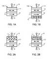
- FIGS. 1A and 1Bare cross-sectional schematic diagrams of magnetic stacks, in particular, memory cells
- FIGS. 2A and 2Bare cross-sectional schematic diagrams of the magnetic stack in a first state ( FIG. 2A ) and in a second state ( FIG. 2B );
- FIG. 3is a process flow diagram for a method of making a magnetic stack
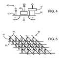
- FIG. 4is a schematic diagram of an illustrative memory unit including a memory cell and a semiconductor transistor
- FIG. 5is a schematic diagram of an illustrative memory array.
- This disclosureis directed to magnetic stacks (e.g., spin torque memory (STRAM) cells and magnetic read sensors) that include a metal oxide layer proximate the free layer that at low temperature is antiferromagnetic but at a high temperature is non-magnetic.
- STRAMspin torque memory
- the metal oxide layerresults in reduction of the effective spin torque barrier due to magnetic moment fluctuation and disorder, thermal assisted switching, and spin specular reflection.
- the metal oxide layeris easy to control and fabricate, forms a natural interface with the free layer, and the pinning strength of the metal oxide layer is easily tunable.
- FIGS. 1A and 1Bare cross-sectional schematic diagram of a magnetic stack 10 A.
- magnetic stack 10 Ais a magnetic read sensor such as a magnetic read sensor used in a rotating magnetic storage device.
- magnetic stack 10 Ais a magnetic memory cell 10 A and may be referred to as a magnetic tunnel junction cell (MTJ), variable resistive memory cell, variable resistance memory cell, or resistive sense memory (RSM) cell or the like.
- Magnetic cell 10 Aincludes a ferromagnetic free layer 12 and a ferromagnetic reference (i.e., pinned) layer 14 , each having a magnetization orientation. Ferromagnetic free layer 12 and ferromagnetic reference layer 14 are separated by a non-magnetic spacer layer 13 . Note that other layers, such as seed or capping layers, are not depicted for clarity but could be included as technical need arises.
- Ferromagnetic layers 12 , 14may be made of any useful ferromagnetic (FM) material such as, for example, Fe, Co or Ni and alloys thereof, such as NiFe and CoFe, and ternary alloys, such as CoFeB.
- FMferromagnetic
- Either or both of free layer 12 and reference layer 14may be either a single layer or a synthetic antiferromagnetic (SAF) coupled structure, i.e., two ferromagnetic sublayers separated by a metallic spacer, such as Ru or Cr, with the magnetization orientations of the sublayers in opposite directions to provide a net magnetization.
- SAFsynthetic antiferromagnetic
- Free layer 12may be a synthetic ferromagnetic coupled structure, i.e., two ferromagnetic sublayers separated by a metallic spacer, such as Ru or Ta, with the magnetization orientations of the sublayers in parallel directions.
- ferromagnetic layers 12 , 14particularly free layer 12 , is formed of a ferromagnetic material with acceptable anisotropy and a saturation moment (Ms) that is at least 500 emu/cc, in some embodiments at least 1100 emu/cc, and in yet other embodiments at least 1500 emu/cc, where emu refers to electromagnetic unit of magnetic dipole moment and cc refers to cubic centimeter.
- Mssaturation moment
- Either or both layers 12 , 14are often about 0.1-10 nm thick, depending on the material and the desired resistance and switchability of free layer 12 .
- free layer 12is thinner than reference layer 14 .
- free layer 12 of the magnetic stacks of this disclosurecan be thinner than free layers of other magnetic stacks.
- Non-magnetic spacer layer 13is an insulating barrier layer sufficiently thin to allow tunneling of charge carriers between reference layer 14 and free layer 12 .
- suitable electrically insulating materialinclude oxides material (e.g., Al 2 O 3 , TiO x or MgO).
- Non-magnetic spacer layer 13could optionally be patterned with free layer 12 or with reference layer 14 , depending on process feasibility and device reliability.
- proximate ferromagnetic reference layer 14is an antiferromagnetic (AFM) pinning layer 15 , which pins the magnetization orientation of ferromagnetic reference layer 14 by exchange bias with the antiferromagnetically ordered material of pinning layer 15 .
- AFMantiferromagnetic
- suitable pinning materialsinclude PtMn, IrMn, and others.
- other mechanisms or elementsmay be used to pin the magnetization orientation of reference layer 14 . Note that other layers, such as seed or capping layers, are not depicted for clarity.
- magnetic stack or cell 10 Aincludes a metal oxide layer 16 proximate ferromagnetic free layer 12 .
- Metal oxide layer 16is positioned so that free layer 12 is between spacer layer 13 and metal oxide layer 16 . In some embodiments, there is no intervening layer between metal oxide layer 16 and free layer 12 .
- Metal oxide layer 16is antiferromagnetic at a first (i.e., low) temperature and is non-magnetic at a second (i.e., high) temperature. In other words, metal oxide layer 16 has a variable magnetization, depending on its temperature.
- metal oxide layer 16When metal oxide layer 16 is in its antiferromagnetic state (see FIG. 2A ), magnetic moments 17 of adjacent atoms of layer 16 are ordered and point in opposite directions.
- metal oxide layer 16is in its non-magnetic state (see FIG. 2B ), magnetic moments 17 are disordered and randomly fluctuate.
- metal oxide layer 16is antiferromagnetic, but changes to non-magnetic at temperatures greater than room temperature, for example, several tens of degrees to a hundred degrees higher.
- metal oxide layer 16is antiferromagnetic at temperatures less than 200° C. and is non-magnetic at temperatures greater than 200° C. In other embodiments, metal oxide layer 16 is antiferromagnetic at temperatures less than 150° C. and is non-magnetic at temperatures greater than 150° C. In still other embodiments, metal oxide layer 16 is antiferromagnetic at temperatures less than 100° C. and is non-magnetic at temperatures greater than 100° C.
- metal oxide layer 16examples include Co and Co alloy oxides (e.g., CoO x ), Fe and Fe alloy oxides (e.g., FeO x , FeMnO x ), and Ni and Ni alloy oxides (e.g., NiO x ) Other metals or alloy oxides may additionally have the required properties, of being ferromagnetic at low temperature and non-magnetic at high temperature.
- Metal oxide layer 16may be formed of one or more materials, which either individually or together provide the required properties. If metal oxide layer 16 is formed of multiple materials, these materials may be present as domains of one material present in a matrix of another material, or may be stacked layers of materials.
- metal oxide layer 16may be a multilayered structure, such as a laminated multilayer structure. The material of metal oxide layer 16 is, in most embodiments, homogenous across its width and length.
- Metal oxide layer 16is often about 5-30 Angstroms thick (e.g., about 10-20 Angstroms), depending on the material of metal oxide layer 16 and the adjacent free layer 12 . In some embodiments, metal oxide layer 16 may be a non-continuous and/or non-contiguous layer.
- Electrodes 18 , 19electrically connect ferromagnetic layers 12 , 14 to a control circuit providing read and write currents through layers 12 , 14 .
- the resistance across magnetic cell 10 A, 10 B, and thus data stateis determined by the relative orientation of the magnetization vectors or orientations of ferromagnetic layers 12 , 14 .
- the magnetization direction of ferromagnetic reference layer 14is pinned in a predetermined direction while the magnetization direction of ferromagnetic free layer 12 is free to rotate under the influence of spin torque, which may be the result of current passing through cell 10 A, 10 B or orthogonal to cell 10 A, 10 B.
- spin torquewhich may be the result of current passing through cell 10 A, 10 B or orthogonal to cell 10 A, 10 B.
- the reading processwhich may be with a current of about 10 ⁇ A and at a temperature less than about 90° C.
- metal oxide layer 16is antiferromagnetic whereas during the writing process, which is at a much higher temperature (e.g., in some embodiments about 100-200° C.), metal oxide layer 16 is non-magnetic.
- the magnetization orientation of free layer 12is illustrated as undefined.
- the magnetization orientation of free layer 12will generally be either parallel to the magnetization orientation of reference layer 14 (i.e., the low resistance state) or anti-parallel to the magnetization orientation of reference layer 14 (i.e., the high resistance state).
- the low resistance statemay be the “0” data state and the high resistance state the “1” data state, whereas in other embodiments, the low resistance state may be “1” and the high resistance state “0”.
- the magnetization orientation of free layer 12can be changed among different directions and accordingly, the magnetic cell can be switched between the parallel state, the anti-parallel state, and other states.
- the magnetization orientation of free layer 12is influenced by a neighboring magnetic field, such as located on magnetic recording medium. When a sufficient magnetic field is applied to free layer 12 , the magnetization orientation of free layer 12 can be changed among different directions, between the parallel state, the anti-parallel state, and other states.
- metal oxide layer 16being antiferromagnetic at low temperatures and non-magnetic at high temperatures, allow the use of lower switching current (e.g., no more than about 100-500 ⁇ A (about 0.1-0.5 mA)) while maintaining thermal stability of the magnetization orientations, than if no metal oxide layer was present. In some embodiments, the switching current is no more than 400 ⁇ A, in other embodiments no more than about 200 ⁇ A. When no switching current is present, metal oxide layer 16 is at a low temperature and is antiferromagnetic. The adjacent free layer 12 is stabilized by the antiferromagnetic metal oxide layer 16 due to the exchange coupling at the interface of free layer 12 and metal oxide layer 16 .
- switching currente.g., no more than about 100-500 ⁇ A (about 0.1-0.5 mA)
- the switching currentis no more than 400 ⁇ A, in other embodiments no more than about 200 ⁇ A.
- metal oxide layer 16provides a pinning effect on free layer 12 (which increases thermal stability of free layer), a thinner free layer 12 has the same level of stability as a thicker free layer with no adjacent metal oxide layer. In some embodiments, the total thickness of free layer 12 and metal oxide layer 16 has the same level of stability as a thicker free layer with no adjacent metal oxide layer. Because the blocking temperature of the metal oxide is low (e.g., about 100° C., or about 150° C.), there is no issue regarding temperature variation from one cell 10 A, 10 B to an adjacent cell when applying a switching current to cell 10 A, 10 B or to the adjacent cell. The antiferromagnetic material confines thermal dissipation to the cell being written and thus reduces the necessary switching current.
- metal oxide layer 16When switching current is present for cell 10 A, 10 B, metal oxide layer 16 is at a high temperature and is non-magnetic.
- the non-magnetic metal oxide layer 16is less stabilizing to free layer 12 than the antiferromagnetic metal oxide layer 16 , thus allowing free layer 12 to readily switch. Additionally, the non-magnetic property provides a spin specular (e.g., reflective) effect within free layer 12 , thus reducing the needed switching current for that cell 10 A, 10 B.
- a non-continuous or non-contiguous metal oxide layer 16may further reduce the switching current by focusing the current and increasing the current density through free layer 12 .
- the magnetic stacks of this disclosuremay be made by thin film techniques such as chemical vapor deposition (CVD), physical vapor deposition (PVD), and atomic layer deposition (ALD).
- PVDphysical vapor deposition
- ALDatomic layer deposition
- Metal oxide layer 16may be formed on free layer 12 by oxidizing a portion of free layer 12 or by applying as a separate layer.
- metal oxide layer 16 formed from oxidized free layer 12depends on the magnetic transport property of free layer 12 (e.g., the magnetic resistance (MR) ratio of free layer 12 and its oxide) and the blocking temperature of oxide layer 16 .
- MRmagnetic resistance
- CoFeB and NiFeBare preferred free layer materials and their oxides, CoO and NiO, respectively, have good tenability and reasonable blocking temperatures.
- CoFewhich has a lower MR, is also acceptable.
- FIG. 3illustrates two methods for forming a magnetic stack having a metal oxide layer.
- the magnetic stacki.e., including reference layer 14 , spacer 13 and free layer 12 .
- the first method for forming metal oxide layer 16includes oxidizing metal oxide layer 16 (Step 31 ) by exposing free layer 12 to an oxygen-rich environment.
- the thickness of the resulting thin layer of oxidedepends on various processing factors such as the level of oxygen, the temperature, and the duration of exposure.
- free layer 12may be heated to facilitate oxidation.
- the oxidation of free layer 12 to form metal oxide layer 16is via plasma oxidation (i.e., using O 2 plasma).
- the thickness and quality of the resulting thin layer of oxidedepends on factors such as O 2 pressure, temperature, and plasma power.
- the second method of forming metal oxide layer 16is to directly form (e.g., deposit) onto free layer 12 (Step 32 ).
- the antiferromagnetic oxide selectedmay be different than the ferromagnetic material, allowing for device optimization.
- a metal oxide layer 16 of NiOmay be deposited onto a free layer 12 formed of CoFeB.
- the deposition of layer 16may be done, for example, by reactive sputtering.
- FIG. 4is a schematic diagram of an illustrative memory unit 40 including a memory element 41 electrically coupled to a semiconductor transistor 42 via an electrically conducting element 44 .
- Memory element 41may be any of the memory cells described herein.
- Transistor 42includes a semiconductor substrate 45 having doped regions (e.g., illustrated as n-doped regions) and a channel region (e.g., illustrated as a p-doped channel region) between the doped regions.
- Transistor 42includes a gate 46 that is electrically coupled to a word line WL to allow selection and current to flow from a bit line BL to memory element 41 .
- An array of memory units 40can be formed on a semiconductor substrate utilizing semiconductor fabrication techniques.
- FIG. 5is a schematic diagram of an illustrative memory array 50 .
- Memory array 50includes a plurality of word lines WL and a plurality of bit lines BL forming a cross-point array. At each cross-point a memory element 51 is electrically coupled to word line WL and bit line BL.
- Memory element 51may be any of the memory cells described herein.
Landscapes
- Engineering & Computer Science (AREA)
- Chemical & Material Sciences (AREA)
- Nanotechnology (AREA)
- Crystallography & Structural Chemistry (AREA)
- Manufacturing & Machinery (AREA)
- Computer Hardware Design (AREA)
- Power Engineering (AREA)
- Physics & Mathematics (AREA)
- Spectroscopy & Molecular Physics (AREA)
- Condensed Matter Physics & Semiconductors (AREA)
- General Physics & Mathematics (AREA)
- Mram Or Spin Memory Techniques (AREA)
- Hall/Mr Elements (AREA)
Abstract
Description
Claims (20)
Priority Applications (2)
| Application Number | Priority Date | Filing Date | Title |
|---|---|---|---|
| US13/248,360US8426222B2 (en) | 2008-10-10 | 2011-09-29 | Magnetic stack with oxide to reduce switching current |
| US13/491,763US8686524B2 (en) | 2008-10-10 | 2012-06-08 | Magnetic stack with oxide to reduce switching current |
Applications Claiming Priority (3)
| Application Number | Priority Date | Filing Date | Title |
|---|---|---|---|
| US10440008P | 2008-10-10 | 2008-10-10 | |
| US12/425,466US8217478B2 (en) | 2008-10-10 | 2009-04-17 | Magnetic stack with oxide to reduce switching current |
| US13/248,360US8426222B2 (en) | 2008-10-10 | 2011-09-29 | Magnetic stack with oxide to reduce switching current |
Related Parent Applications (1)
| Application Number | Title | Priority Date | Filing Date |
|---|---|---|---|
| US12/425,466DivisionUS8217478B2 (en) | 2008-10-10 | 2009-04-17 | Magnetic stack with oxide to reduce switching current |
Related Child Applications (1)
| Application Number | Title | Priority Date | Filing Date |
|---|---|---|---|
| US13/491,763ContinuationUS8686524B2 (en) | 2008-10-10 | 2012-06-08 | Magnetic stack with oxide to reduce switching current |
Publications (2)
| Publication Number | Publication Date |
|---|---|
| US20120021535A1 US20120021535A1 (en) | 2012-01-26 |
| US8426222B2true US8426222B2 (en) | 2013-04-23 |
Family
ID=42098105
Family Applications (3)
| Application Number | Title | Priority Date | Filing Date |
|---|---|---|---|
| US12/425,466Expired - Fee RelatedUS8217478B2 (en) | 2008-10-10 | 2009-04-17 | Magnetic stack with oxide to reduce switching current |
| US13/248,360ActiveUS8426222B2 (en) | 2008-10-10 | 2011-09-29 | Magnetic stack with oxide to reduce switching current |
| US13/491,763ActiveUS8686524B2 (en) | 2008-10-10 | 2012-06-08 | Magnetic stack with oxide to reduce switching current |
Family Applications Before (1)
| Application Number | Title | Priority Date | Filing Date |
|---|---|---|---|
| US12/425,466Expired - Fee RelatedUS8217478B2 (en) | 2008-10-10 | 2009-04-17 | Magnetic stack with oxide to reduce switching current |
Family Applications After (1)
| Application Number | Title | Priority Date | Filing Date |
|---|---|---|---|
| US13/491,763ActiveUS8686524B2 (en) | 2008-10-10 | 2012-06-08 | Magnetic stack with oxide to reduce switching current |
Country Status (1)
| Country | Link |
|---|---|
| US (3) | US8217478B2 (en) |
Cited By (1)
| Publication number | Priority date | Publication date | Assignee | Title |
|---|---|---|---|---|
| US9460397B2 (en) | 2013-10-04 | 2016-10-04 | Samsung Electronics Co., Ltd. | Quantum computing device spin transfer torque magnetic memory |
Families Citing this family (16)
| Publication number | Priority date | Publication date | Assignee | Title |
|---|---|---|---|---|
| US8169810B2 (en)* | 2008-10-08 | 2012-05-01 | Seagate Technology Llc | Magnetic memory with asymmetric energy barrier |
| US8546896B2 (en)* | 2010-07-16 | 2013-10-01 | Grandis, Inc. | Magnetic tunneling junction elements having magnetic substructures(s) with a perpendicular anisotropy and memories using such magnetic elements |
| US8456894B2 (en)* | 2011-05-03 | 2013-06-04 | International Business Machines Corporation | Noncontact writing of nanometer scale magnetic bits using heat flow induced spin torque effect |
| US8754491B2 (en) | 2011-05-03 | 2014-06-17 | International Business Machines Corporation | Spin torque MRAM using bidirectional magnonic writing |
| US8456895B2 (en) | 2011-05-03 | 2013-06-04 | International Business Machines Corporation | Magnonic magnetic random access memory device |
| US8592929B2 (en) | 2011-09-12 | 2013-11-26 | Qualcomm Incorporated | Symmetrically switchable spin-transfer-torque magnetoresistive device |
| WO2013086068A1 (en)* | 2011-12-06 | 2013-06-13 | University Of North Texas | Direct graphene growth on metal oxides by molecular beam epitaxy |
| US8921961B2 (en) | 2012-09-14 | 2014-12-30 | Headway Technologies, Inc. | Storage element for STT MRAM applications |
| US8796797B2 (en) | 2012-12-21 | 2014-08-05 | Intel Corporation | Perpendicular spin transfer torque memory (STTM) device with enhanced stability and method to form same |
| US8971103B2 (en) | 2013-03-13 | 2015-03-03 | International Business Machines Corporation | Thermally-assisted MRAM with ferromagnetic layers with temperature dependent magnetization |
| US9779865B2 (en)* | 2014-10-17 | 2017-10-03 | The Arizona Board Of Regents On Behalf Of The University Of Arizona | Voltage-controlled magnetic devices |
| US10272572B2 (en)* | 2016-06-10 | 2019-04-30 | The Boeing Company | Remotely controlling robotic platforms based on multi-modal sensory data |
| US9734850B1 (en)* | 2016-06-28 | 2017-08-15 | Western Digital Technologies, Inc. | Magnetic tunnel junction (MTJ) free layer damping reduction |
| WO2018182651A1 (en)* | 2017-03-30 | 2018-10-04 | Intel Corporation | Perpendicular spin transfer torque memory (psttm) devices with enhanced anisotropy and methods to form the same |
| CN108320768A (en)* | 2018-01-19 | 2018-07-24 | 上海磁宇信息科技有限公司 | It is a kind of to use the magnetic RAM for reinforcing logic gates |
| CN118510374A (en)* | 2023-02-14 | 2024-08-16 | 中国科学院物理研究所 | Magnonic junctions, magnon random access memory, microwave oscillations and detectors, electronic devices |
Citations (124)
| Publication number | Priority date | Publication date | Assignee | Title |
|---|---|---|---|---|
| US5461526A (en) | 1992-03-24 | 1995-10-24 | Hitachi, Ltd. | Magnetoresistive read head and magnetic storage system using the same |
| US5841692A (en) | 1996-03-18 | 1998-11-24 | International Business Machines Corporation | Magnetic tunnel junction device with antiferromagnetically coupled pinned layer |
| US5963472A (en) | 1994-12-27 | 1999-10-05 | Nkk Corporation | Information storage apparatus and method for operating the same |
| US6146775A (en) | 1996-11-18 | 2000-11-14 | Sanyo Electric Co., Ltd. | Magnetoresistive film |
| US6166948A (en) | 1999-09-03 | 2000-12-26 | International Business Machines Corporation | Magnetic memory array with magnetic tunnel junction memory cells having flux-closed free layers |
| US6183859B1 (en) | 1998-07-20 | 2001-02-06 | Motorola, Inc | Low resistance MTJ |
| US20020186582A1 (en) | 2001-04-02 | 2002-12-12 | Manish Sharma | Cladded read conductor for a pinned-on-the-fly soft reference layer |
| US6522573B2 (en) | 2000-06-30 | 2003-02-18 | Kabushiki Kaisha Toshiba | Solid-state magnetic memory using ferromagnetic tunnel junctions |
| US6597618B2 (en) | 2001-12-04 | 2003-07-22 | Data Storage Institute | Magnetic tunnel junction magnetic random access memory |
| US20030143431A1 (en) | 2002-01-25 | 2003-07-31 | Naoya Hasegawa | CPP magnetic sensing element in which pinned magnetic layers of upper and lower multilayer films are magnetized antiparallel to each other, method for making the same, and magnetic sensing device including the same |
| US6605772B2 (en) | 1999-08-27 | 2003-08-12 | Massachusetts Institute Of Technology | Nanostructured thermoelectric materials and devices |
| US6633498B1 (en) | 2002-06-18 | 2003-10-14 | Motorola, Inc. | Magnetoresistive random access memory with reduced switching field |
| US20030231437A1 (en)* | 2002-06-17 | 2003-12-18 | Childress Jeffrey R. | Current-perpendicular-to-plane magnetoresistive device with oxidized free layer side regions and method for its fabrication |
| US6714444B2 (en) | 2002-08-06 | 2004-03-30 | Grandis, Inc. | Magnetic element utilizing spin transfer and an MRAM device using the magnetic element |
| US20040084702A1 (en) | 2002-11-01 | 2004-05-06 | Won-Cheol Jeong | Magnetic memories with bit lines and digit lines that intersect at oblique angles and fabrication methods thereof |
| US6771534B2 (en) | 2002-11-15 | 2004-08-03 | International Business Machines Corporation | Thermally-assisted magnetic writing using an oxide layer and current-induced heating |
| US6781874B2 (en) | 2001-08-02 | 2004-08-24 | Renesas Technology Corp. | Thin film magnetic memory device including memory cells having a magnetic tunnel junction |
| US20040165320A1 (en)* | 2003-02-24 | 2004-08-26 | Carey Matthew J. | Magnetoresistive device with exchange-coupled structure having half-metallic ferromagnetic heusler alloy in the pinned layer |
| US6791865B2 (en) | 2002-09-03 | 2004-09-14 | Hewlett-Packard Development Company, L.P. | Memory device capable of calibration and calibration methods therefor |
| US6819586B1 (en) | 2003-10-24 | 2004-11-16 | Hewlett-Packard Development Company, L.P. | Thermally-assisted magnetic memory structures |
| US6829161B2 (en) | 2003-01-10 | 2004-12-07 | Grandis, Inc. | Magnetostatically coupled magnetic elements utilizing spin transfer and an MRAM device using the magnetic element |
| US6838740B2 (en) | 2002-09-27 | 2005-01-04 | Grandis, Inc. | Thermally stable magnetic elements utilizing spin transfer and an MRAM device using the magnetic element |
| US6845038B1 (en) | 2003-02-01 | 2005-01-18 | Alla Mikhailovna Shukh | Magnetic tunnel junction memory device |
| US6847547B2 (en) | 2003-02-28 | 2005-01-25 | Grandis, Inc. | Magnetostatically coupled magnetic elements utilizing spin transfer and an MRAM device using the magnetic element |
| US20050018475A1 (en) | 2003-07-22 | 2005-01-27 | Lung Tran | Magnetic memory structure |
| US6888742B1 (en) | 2002-08-28 | 2005-05-03 | Grandis, Inc. | Off-axis pinned layer magnetic element utilizing spin transfer and an MRAM device using the magnetic element |
| US20050104146A1 (en) | 2003-11-14 | 2005-05-19 | Nickel Janice H. | Thin film device and a method of providing thermal assistance therein |
| US6903400B2 (en) | 2003-10-06 | 2005-06-07 | Fujitsu Limited | Magnetoresistive memory apparatus |
| US20050150537A1 (en) | 2004-01-13 | 2005-07-14 | Nanocoolers Inc. | Thermoelectric devices |
| US20050150535A1 (en) | 2004-01-13 | 2005-07-14 | Nanocoolers, Inc. | Method for forming a thin-film thermoelectric device including a phonon-blocking thermal conductor |
| US6933155B2 (en) | 2003-05-21 | 2005-08-23 | Grandis, Inc. | Methods for providing a sub .15 micron magnetic memory structure |
| US6950335B2 (en) | 2001-11-16 | 2005-09-27 | Commissariat A L'energie Atomique | Magnetic tunnel junction magnetic device, memory and writing and reading methods using said device |
| US6958927B1 (en) | 2002-10-09 | 2005-10-25 | Grandis Inc. | Magnetic element utilizing spin-transfer and half-metals and an MRAM device using the magnetic element |
| US6963098B2 (en) | 2003-06-23 | 2005-11-08 | Nve Corporation | Thermally operated switch control memory cell |
| US6967863B2 (en) | 2004-02-25 | 2005-11-22 | Grandis, Inc. | Perpendicular magnetization magnetic element utilizing spin transfer |
| US6980464B2 (en) | 2002-09-10 | 2005-12-27 | Kabushiki Kaisha Toshiba | Magnetic random access memory |
| US6980469B2 (en) | 2003-08-19 | 2005-12-27 | New York University | High speed low power magnetic devices based on current induced spin-momentum transfer |
| US6985385B2 (en) | 2003-08-26 | 2006-01-10 | Grandis, Inc. | Magnetic memory element utilizing spin transfer switching and storing multiple bits |
| US6992359B2 (en) | 2004-02-26 | 2006-01-31 | Grandis, Inc. | Spin transfer magnetic element with free layers having high perpendicular anisotropy and in-plane equilibrium magnetization |
| US7006336B2 (en) | 2002-08-06 | 2006-02-28 | International Business Machines Corporation | Magnetic head having a heater circuit for thermally-assisted writing |
| US7020009B2 (en) | 2003-05-14 | 2006-03-28 | Macronix International Co., Ltd. | Bistable magnetic device using soft magnetic intermediary material |
| US7031178B2 (en) | 2003-06-10 | 2006-04-18 | International Business Machines Corporation | Magnetic shift register with shiftable magnetic domains between two regions, and method of using the same |
| US7057921B2 (en) | 2004-05-11 | 2006-06-06 | Grandis, Inc. | Spin barrier enhanced dual magnetoresistance effect element and magnetic memory using the same |
| US7088609B2 (en) | 2004-05-11 | 2006-08-08 | Grandis, Inc. | Spin barrier enhanced magnetoresistance effect element and magnetic memory using the same |
| US7098494B2 (en) | 2004-06-16 | 2006-08-29 | Grandis, Inc. | Re-configurable logic elements using heat assisted magnetic tunneling elements |
| US7110287B2 (en) | 2004-02-13 | 2006-09-19 | Grandis, Inc. | Method and system for providing heat assisted switching of a magnetic element utilizing spin transfer |
| US20060215444A1 (en) | 2005-03-24 | 2006-09-28 | Perner Frederick A | Series diode thermally assisted MRAM |
| US7126202B2 (en) | 2004-11-16 | 2006-10-24 | Grandis, Inc. | Spin scattering and heat assisted switching of a magnetic element |
| US7161829B2 (en) | 2003-09-19 | 2007-01-09 | Grandis, Inc. | Current confined pass layer for magnetic elements utilizing spin-transfer and an MRAM device using such magnetic elements |
| US7160770B2 (en) | 1998-07-17 | 2007-01-09 | Murata Manufacturing Co., Ltd. | Method of manufacturing an electronic component including an inter-line insulating layer and a conductor pattern |
| US20070034919A1 (en) | 2005-08-09 | 2007-02-15 | Maglc Technologies, Inc. | MRAM with super-paramagnetic sensing layer |
| US7180113B2 (en) | 2005-02-10 | 2007-02-20 | Infineon Technologies Ag | Double-decker MRAM cell with rotated reference layer magnetizations |
| US7187577B1 (en) | 2005-11-23 | 2007-03-06 | Grandis, Inc. | Method and system for providing current balanced writing for memory cells and magnetic devices |
| US7190611B2 (en) | 2003-01-07 | 2007-03-13 | Grandis, Inc. | Spin-transfer multilayer stack containing magnetic layers with resettable magnetization |
| US7205564B2 (en) | 2003-11-11 | 2007-04-17 | Kabushiki Kaisha Toshiba | Resistance change memory having organic semiconductor layer |
| US20070085068A1 (en) | 2005-10-14 | 2007-04-19 | Dmytro Apalkov | Spin transfer based magnetic storage cells utilizing granular free layers and magnetic memories using such cells |
| US7224601B2 (en) | 2005-08-25 | 2007-05-29 | Grandis Inc. | Oscillating-field assisted spin torque switching of a magnetic tunnel junction memory element |
| US7230845B1 (en) | 2005-07-29 | 2007-06-12 | Grandis, Inc. | Magnetic devices having a hard bias field and magnetic memory devices using the magnetic devices |
| US7230265B2 (en) | 2005-05-16 | 2007-06-12 | International Business Machines Corporation | Spin-polarization devices using rare earth-transition metal alloys |
| US7233039B2 (en) | 2004-04-21 | 2007-06-19 | Grandis, Inc. | Spin transfer magnetic elements with spin depolarization layers |
| US7241631B2 (en) | 2004-12-29 | 2007-07-10 | Grandis, Inc. | MTJ elements with high spin polarization layers configured for spin-transfer switching and spintronics devices using the magnetic elements |
| US7242048B2 (en) | 2003-12-22 | 2007-07-10 | Grandis, Inc. | Magnetic elements with ballistic magnetoresistance utilizing spin-transfer and an MRAM device using such magnetic elements |
| US7242045B2 (en) | 2004-02-19 | 2007-07-10 | Grandis, Inc. | Spin transfer magnetic element having low saturation magnetization free layers |
| US7245462B2 (en) | 2003-08-21 | 2007-07-17 | Grandis, Inc. | Magnetoresistive element having reduced spin transfer induced noise |
| US20070176251A1 (en) | 2006-01-27 | 2007-08-02 | Se-Chung Oh | Magnetic memory device and method of fabricating the same |
| US7252852B1 (en) | 2003-12-12 | 2007-08-07 | International Business Machines Corporation | Mg-Zn oxide tunnel barriers and method of formation |
| US7272035B1 (en) | 2005-08-31 | 2007-09-18 | Grandis, Inc. | Current driven switching of magnetic storage cells utilizing spin transfer and magnetic memories using such cells |
| US7272034B1 (en) | 2005-08-31 | 2007-09-18 | Grandis, Inc. | Current driven switching of magnetic storage cells utilizing spin transfer and magnetic memories using such cells |
| US7274057B2 (en) | 2004-04-26 | 2007-09-25 | International Business Machines Corporation | Techniques for spin-flop switching with offset field |
| US7282755B2 (en) | 2003-11-14 | 2007-10-16 | Grandis, Inc. | Stress assisted current driven switching for magnetic memory applications |
| US7286395B2 (en) | 2005-10-27 | 2007-10-23 | Grandis, Inc. | Current driven switched magnetic storage cells having improved read and write margins and magnetic memories using such cells |
| US7289356B2 (en) | 2005-06-08 | 2007-10-30 | Grandis, Inc. | Fast magnetic memory devices utilizing spin transfer and magnetic elements used therein |
| US20070258281A1 (en) | 2006-05-04 | 2007-11-08 | Kenchi Ito | Magnetic memory device |
| US7310265B2 (en) | 2003-10-14 | 2007-12-18 | Agency For Science, Technology And Research | Magnetic memory device |
| US20080019040A1 (en) | 2006-07-21 | 2008-01-24 | Xiaochun Zhu | Perpendicular spin-torque-driven magnetic oscillator |
| US20080037179A1 (en) | 2006-05-04 | 2008-02-14 | Kenchi Ito | Magnetic memory device |
| US7339817B2 (en) | 2001-01-11 | 2008-03-04 | Samsung Electronics Co., Ltd. | Thermally-assisted switching of magnetic memory elements |
| US20080055792A1 (en) | 2006-03-07 | 2008-03-06 | Agency For Science, Technology And Research | Memory cells and devices having magnetoresistive tunnel junction with guided magnetic moment switching and method |
| US7342169B2 (en) | 2001-10-05 | 2008-03-11 | Nextreme Thermal Solutions | Phonon-blocking, electron-transmitting low-dimensional structures |
| US7345911B2 (en) | 2006-02-14 | 2008-03-18 | Magic Technologies, Inc. | Multi-state thermally assisted storage |
| US7345912B2 (en) | 2006-06-01 | 2008-03-18 | Grandis, Inc. | Method and system for providing a magnetic memory structure utilizing spin transfer |
| US7349243B2 (en) | 2006-04-20 | 2008-03-25 | Taiwan Semiconductor Manufacturing Company, Ltd. | 3-parameter switching technique for use in MRAM memory arrays |
| US7369427B2 (en) | 2004-09-09 | 2008-05-06 | Grandis, Inc. | Magnetic elements with spin engineered insertion layers and MRAM devices using the magnetic elements |
| US7372116B2 (en) | 2004-06-16 | 2008-05-13 | Hitachi Global Storage Technologies Netherlands B.V. | Heat assisted switching in an MRAM cell utilizing the antiferromagnetic to ferromagnetic transition in FeRh |
| US20080112094A1 (en) | 2003-08-19 | 2008-05-15 | New York University | High speed low power annular magnetic devices based on current induced spin-momentum transfer |
| US7379327B2 (en) | 2006-06-26 | 2008-05-27 | Grandis, Inc. | Current driven switching of magnetic storage cells utilizing spin transfer and magnetic memories using such cells having enhanced read and write margins |
| US20080137224A1 (en) | 2006-12-06 | 2008-06-12 | Seagate Technology Llc | High frequency field assisted write device |
| US20080154519A1 (en) | 2006-06-13 | 2008-06-26 | International Business Machines Corporation | Quantification of adsorbed molecular contaminant using thin film measurement |
| US20080180827A1 (en) | 2007-01-31 | 2008-07-31 | Carnegie Mellon University | Binary anisotropy media |
| US20080186758A1 (en) | 2007-02-07 | 2008-08-07 | Industrial Technology Research Institute | Magnetic memory device |
| US7411817B2 (en) | 2004-02-23 | 2008-08-12 | Centre National De La Recherche Scientifique | Magnetic memory with a magnetic tunnel junction written in a thermally assisted manner, and method for writing the same |
| US20080225584A1 (en) | 2007-03-16 | 2008-09-18 | Seagate Technology Llc | Magnetic storage element responsive to spin polarized current |
| US7430135B2 (en) | 2005-12-23 | 2008-09-30 | Grandis Inc. | Current-switched spin-transfer magnetic devices with reduced spin-transfer switching current density |
| US20080273380A1 (en) | 2007-03-27 | 2008-11-06 | Grandis | Method and system for providing field biased magnetic memory devices |
| US7453720B2 (en) | 2005-05-26 | 2008-11-18 | Maglabs, Inc. | Magnetic random access memory with stacked toggle memory cells having oppositely-directed easy-axis biasing |
| US20080291720A1 (en) | 2007-05-22 | 2008-11-27 | Taiwan Semiconductor Manufacturing Company, Ltd. | Spin torque transfer mram device |
| US20080291721A1 (en) | 2007-05-21 | 2008-11-27 | Grandis, Inc. | Method and system for providing a spin transfer device with improved switching characteristics |
| US20080310219A1 (en) | 2007-06-12 | 2008-12-18 | Grandis, Inc. | Method and system for providing a magnetic element and magnetic memory being unidirectional writing enabled |
| US20080310213A1 (en) | 2007-06-15 | 2008-12-18 | Grandis, Inc. | Method and system for providing spin transfer tunneling magnetic memories utilizing non-planar transistors |
| US20090010040A1 (en) | 2007-06-29 | 2009-01-08 | Kabushiki Kaisha Toshiba | Resistance change memory device |
| US7479193B1 (en) | 2004-02-12 | 2009-01-20 | The United States Of America As Represented By The Secretary Of The Navy | Preparation of positive magnetostrictive materials for use under tension |
| US7486551B1 (en) | 2007-04-03 | 2009-02-03 | Grandis, Inc. | Method and system for providing domain wall assisted switching of magnetic elements and magnetic memories using such magnetic elements |
| US7486545B2 (en) | 2005-11-01 | 2009-02-03 | Magic Technologies, Inc. | Thermally assisted integrated MRAM design and process for its manufacture |
| US7489541B2 (en) | 2005-08-23 | 2009-02-10 | Grandis, Inc. | Spin-transfer switching magnetic elements using ferrimagnets and magnetic memories using the magnetic elements |
| US20090040855A1 (en) | 2007-08-07 | 2009-02-12 | Grandis, Inc. | Method and system for providing a sense amplifier and drive circuit for spin transfer torque magnetic random access memory |
| US20090050991A1 (en) | 2007-08-22 | 2009-02-26 | Hide Nagai | Magnetic Element Having Low Saturation Magnetization |
| US7502249B1 (en) | 2006-07-17 | 2009-03-10 | Grandis, Inc. | Method and system for using a pulsed field to assist spin transfer induced switching of magnetic memory elements |
| US20090073750A1 (en) | 2007-09-17 | 2009-03-19 | Rainer Leuschner | Method for Programming an Integrated Circuit, Methods for Programming a Plurality of Cells, Integrated Circuit, Cell Arrangement |
| US7508702B2 (en) | 2007-04-17 | 2009-03-24 | Macronix International Co., Ltd. | Programming method of magnetic random access memory |
| US7515457B2 (en) | 2006-02-24 | 2009-04-07 | Grandis, Inc. | Current driven memory cells having enhanced current and enhanced current symmetry |
| US7518835B2 (en) | 2005-07-01 | 2009-04-14 | Grandis, Inc. | Magnetic elements having a bias field and magnetic memory devices using the magnetic elements |
| US7525862B1 (en) | 2008-05-09 | 2009-04-28 | International Business Machines Corporation | Methods involving resetting spin-torque magnetic random access memory with domain wall |
| US20090185410A1 (en) | 2008-01-22 | 2009-07-23 | Grandis, Inc. | Method and system for providing spin transfer tunneling magnetic memories utilizing unidirectional polarity selection devices |
| US7576956B2 (en) | 2004-07-26 | 2009-08-18 | Grandis Inc. | Magnetic tunnel junction having diffusion stop layer |
| US20090302403A1 (en) | 2008-06-05 | 2009-12-10 | Nguyen Paul P | Spin torque transfer magnetic memory cell |
| US20100034008A1 (en) | 2008-08-07 | 2010-02-11 | Seagate Technology Llc | Magnetic field assisted stram cells |
| US20100091564A1 (en) | 2008-10-10 | 2010-04-15 | Seagate Technology Llc | Magnetic stack having reduced switching current |
| US20100157658A1 (en) | 2008-12-19 | 2010-06-24 | Unity Semiconductor Corporation | Conductive metal oxide structures in non-volatile re-writable memory devices |
| US20100155722A1 (en) | 2008-12-19 | 2010-06-24 | Unity Semiconductor Corporation | Memory device with band gap control |
| US20100155953A1 (en) | 2008-12-19 | 2010-06-24 | Unity Semiconductor Corporation | Conductive oxide electrodes |
| US7800095B2 (en) | 2006-12-26 | 2010-09-21 | Samsung Electronics Co., Ltd. | Phase-change memory device having phase change material pattern shared between adjacent cells and electronic product including the phase-change memory |
| US7804709B2 (en) | 2008-07-18 | 2010-09-28 | Seagate Technology Llc | Diode assisted switching spin-transfer torque memory unit |
| US7821818B2 (en) | 2005-10-14 | 2010-10-26 | Comissariat a l'Energie Atomique et aux Energies Alternatives | Magnetoresistive tunnel junction magnetic device and its application to MRAM |
| US7936585B2 (en) | 2009-07-13 | 2011-05-03 | Seagate Technology Llc | Non-volatile memory cell with non-ohmic selection layer |
Family Cites Families (8)
| Publication number | Priority date | Publication date | Assignee | Title |
|---|---|---|---|---|
| US780095A (en)* | 1905-01-17 | Max Gehre | Pressure-gage. | |
| JP3629309B2 (en)* | 1995-09-05 | 2005-03-16 | アルプス電気株式会社 | Thin film magnetic head |
| AU2002230524A1 (en)* | 2000-11-16 | 2002-05-27 | California Institute Of Technology | Apparatus and methods for conducting assays and high throughput screening |
| US6872612B2 (en) | 2001-06-27 | 2005-03-29 | Lsi Logic Corporation | Local interconnect for integrated circuit |
| JP2004200245A (en) | 2002-12-16 | 2004-07-15 | Nec Corp | Magnetoresistive element and manufacturing method therefor |
| US7715154B2 (en)* | 2005-04-13 | 2010-05-11 | Seagate Technology Llc | Suppression of spin momentum transfer and related torques in magnetoresistive elements |
| US7777261B2 (en) | 2005-09-20 | 2010-08-17 | Grandis Inc. | Magnetic device having stabilized free ferromagnetic layer |
| US7750333B2 (en)* | 2006-06-28 | 2010-07-06 | Intel Corporation | Bit-erasing architecture for seek-scan probe (SSP) memory storage |
- 2009
- 2009-04-17USUS12/425,466patent/US8217478B2/ennot_activeExpired - Fee Related
- 2011
- 2011-09-29USUS13/248,360patent/US8426222B2/enactiveActive
- 2012
- 2012-06-08USUS13/491,763patent/US8686524B2/enactiveActive
Patent Citations (130)
| Publication number | Priority date | Publication date | Assignee | Title |
|---|---|---|---|---|
| US5461526A (en) | 1992-03-24 | 1995-10-24 | Hitachi, Ltd. | Magnetoresistive read head and magnetic storage system using the same |
| US5963472A (en) | 1994-12-27 | 1999-10-05 | Nkk Corporation | Information storage apparatus and method for operating the same |
| US5841692A (en) | 1996-03-18 | 1998-11-24 | International Business Machines Corporation | Magnetic tunnel junction device with antiferromagnetically coupled pinned layer |
| US6146775A (en) | 1996-11-18 | 2000-11-14 | Sanyo Electric Co., Ltd. | Magnetoresistive film |
| US7160770B2 (en) | 1998-07-17 | 2007-01-09 | Murata Manufacturing Co., Ltd. | Method of manufacturing an electronic component including an inter-line insulating layer and a conductor pattern |
| US6183859B1 (en) | 1998-07-20 | 2001-02-06 | Motorola, Inc | Low resistance MTJ |
| US6605772B2 (en) | 1999-08-27 | 2003-08-12 | Massachusetts Institute Of Technology | Nanostructured thermoelectric materials and devices |
| US6166948A (en) | 1999-09-03 | 2000-12-26 | International Business Machines Corporation | Magnetic memory array with magnetic tunnel junction memory cells having flux-closed free layers |
| US6522573B2 (en) | 2000-06-30 | 2003-02-18 | Kabushiki Kaisha Toshiba | Solid-state magnetic memory using ferromagnetic tunnel junctions |
| US7339817B2 (en) | 2001-01-11 | 2008-03-04 | Samsung Electronics Co., Ltd. | Thermally-assisted switching of magnetic memory elements |
| US20020186582A1 (en) | 2001-04-02 | 2002-12-12 | Manish Sharma | Cladded read conductor for a pinned-on-the-fly soft reference layer |
| US6781874B2 (en) | 2001-08-02 | 2004-08-24 | Renesas Technology Corp. | Thin film magnetic memory device including memory cells having a magnetic tunnel junction |
| US7342169B2 (en) | 2001-10-05 | 2008-03-11 | Nextreme Thermal Solutions | Phonon-blocking, electron-transmitting low-dimensional structures |
| US6950335B2 (en) | 2001-11-16 | 2005-09-27 | Commissariat A L'energie Atomique | Magnetic tunnel junction magnetic device, memory and writing and reading methods using said device |
| US6597618B2 (en) | 2001-12-04 | 2003-07-22 | Data Storage Institute | Magnetic tunnel junction magnetic random access memory |
| US20030143431A1 (en) | 2002-01-25 | 2003-07-31 | Naoya Hasegawa | CPP magnetic sensing element in which pinned magnetic layers of upper and lower multilayer films are magnetized antiparallel to each other, method for making the same, and magnetic sensing device including the same |
| US20030231437A1 (en)* | 2002-06-17 | 2003-12-18 | Childress Jeffrey R. | Current-perpendicular-to-plane magnetoresistive device with oxidized free layer side regions and method for its fabrication |
| US6633498B1 (en) | 2002-06-18 | 2003-10-14 | Motorola, Inc. | Magnetoresistive random access memory with reduced switching field |
| US6714444B2 (en) | 2002-08-06 | 2004-03-30 | Grandis, Inc. | Magnetic element utilizing spin transfer and an MRAM device using the magnetic element |
| US7006336B2 (en) | 2002-08-06 | 2006-02-28 | International Business Machines Corporation | Magnetic head having a heater circuit for thermally-assisted writing |
| US6888742B1 (en) | 2002-08-28 | 2005-05-03 | Grandis, Inc. | Off-axis pinned layer magnetic element utilizing spin transfer and an MRAM device using the magnetic element |
| US6791865B2 (en) | 2002-09-03 | 2004-09-14 | Hewlett-Packard Development Company, L.P. | Memory device capable of calibration and calibration methods therefor |
| US6980464B2 (en) | 2002-09-10 | 2005-12-27 | Kabushiki Kaisha Toshiba | Magnetic random access memory |
| US6838740B2 (en) | 2002-09-27 | 2005-01-04 | Grandis, Inc. | Thermally stable magnetic elements utilizing spin transfer and an MRAM device using the magnetic element |
| US7227773B1 (en) | 2002-10-09 | 2007-06-05 | Grandis, Inc. | Magnetic element utilizing spin-transfer and half-metals and an MRAM device using the magnetic element |
| US6958927B1 (en) | 2002-10-09 | 2005-10-25 | Grandis Inc. | Magnetic element utilizing spin-transfer and half-metals and an MRAM device using the magnetic element |
| US20040084702A1 (en) | 2002-11-01 | 2004-05-06 | Won-Cheol Jeong | Magnetic memories with bit lines and digit lines that intersect at oblique angles and fabrication methods thereof |
| US6771534B2 (en) | 2002-11-15 | 2004-08-03 | International Business Machines Corporation | Thermally-assisted magnetic writing using an oxide layer and current-induced heating |
| US7190611B2 (en) | 2003-01-07 | 2007-03-13 | Grandis, Inc. | Spin-transfer multilayer stack containing magnetic layers with resettable magnetization |
| US6829161B2 (en) | 2003-01-10 | 2004-12-07 | Grandis, Inc. | Magnetostatically coupled magnetic elements utilizing spin transfer and an MRAM device using the magnetic element |
| US6845038B1 (en) | 2003-02-01 | 2005-01-18 | Alla Mikhailovna Shukh | Magnetic tunnel junction memory device |
| US20040165320A1 (en)* | 2003-02-24 | 2004-08-26 | Carey Matthew J. | Magnetoresistive device with exchange-coupled structure having half-metallic ferromagnetic heusler alloy in the pinned layer |
| US6847547B2 (en) | 2003-02-28 | 2005-01-25 | Grandis, Inc. | Magnetostatically coupled magnetic elements utilizing spin transfer and an MRAM device using the magnetic element |
| US7020009B2 (en) | 2003-05-14 | 2006-03-28 | Macronix International Co., Ltd. | Bistable magnetic device using soft magnetic intermediary material |
| US6933155B2 (en) | 2003-05-21 | 2005-08-23 | Grandis, Inc. | Methods for providing a sub .15 micron magnetic memory structure |
| US7031178B2 (en) | 2003-06-10 | 2006-04-18 | International Business Machines Corporation | Magnetic shift register with shiftable magnetic domains between two regions, and method of using the same |
| US6963098B2 (en) | 2003-06-23 | 2005-11-08 | Nve Corporation | Thermally operated switch control memory cell |
| US20050018475A1 (en) | 2003-07-22 | 2005-01-27 | Lung Tran | Magnetic memory structure |
| US7170778B2 (en) | 2003-08-19 | 2007-01-30 | New York University | High speed low power magnetic devices based on current induced spin-momentum transfer |
| US7307876B2 (en) | 2003-08-19 | 2007-12-11 | New York University | High speed low power annular magnetic devices based on current induced spin-momentum transfer |
| US6980469B2 (en) | 2003-08-19 | 2005-12-27 | New York University | High speed low power magnetic devices based on current induced spin-momentum transfer |
| US20080112094A1 (en) | 2003-08-19 | 2008-05-15 | New York University | High speed low power annular magnetic devices based on current induced spin-momentum transfer |
| US7245462B2 (en) | 2003-08-21 | 2007-07-17 | Grandis, Inc. | Magnetoresistive element having reduced spin transfer induced noise |
| US6985385B2 (en) | 2003-08-26 | 2006-01-10 | Grandis, Inc. | Magnetic memory element utilizing spin transfer switching and storing multiple bits |
| US7161829B2 (en) | 2003-09-19 | 2007-01-09 | Grandis, Inc. | Current confined pass layer for magnetic elements utilizing spin-transfer and an MRAM device using such magnetic elements |
| US6903400B2 (en) | 2003-10-06 | 2005-06-07 | Fujitsu Limited | Magnetoresistive memory apparatus |
| US7310265B2 (en) | 2003-10-14 | 2007-12-18 | Agency For Science, Technology And Research | Magnetic memory device |
| US6819586B1 (en) | 2003-10-24 | 2004-11-16 | Hewlett-Packard Development Company, L.P. | Thermally-assisted magnetic memory structures |
| US7205564B2 (en) | 2003-11-11 | 2007-04-17 | Kabushiki Kaisha Toshiba | Resistance change memory having organic semiconductor layer |
| US7282755B2 (en) | 2003-11-14 | 2007-10-16 | Grandis, Inc. | Stress assisted current driven switching for magnetic memory applications |
| US20050104146A1 (en) | 2003-11-14 | 2005-05-19 | Nickel Janice H. | Thin film device and a method of providing thermal assistance therein |
| US7252852B1 (en) | 2003-12-12 | 2007-08-07 | International Business Machines Corporation | Mg-Zn oxide tunnel barriers and method of formation |
| US7242048B2 (en) | 2003-12-22 | 2007-07-10 | Grandis, Inc. | Magnetic elements with ballistic magnetoresistance utilizing spin-transfer and an MRAM device using such magnetic elements |
| US20050150535A1 (en) | 2004-01-13 | 2005-07-14 | Nanocoolers, Inc. | Method for forming a thin-film thermoelectric device including a phonon-blocking thermal conductor |
| US20050150537A1 (en) | 2004-01-13 | 2005-07-14 | Nanocoolers Inc. | Thermoelectric devices |
| US7479193B1 (en) | 2004-02-12 | 2009-01-20 | The United States Of America As Represented By The Secretary Of The Navy | Preparation of positive magnetostrictive materials for use under tension |
| US7110287B2 (en) | 2004-02-13 | 2006-09-19 | Grandis, Inc. | Method and system for providing heat assisted switching of a magnetic element utilizing spin transfer |
| US7242045B2 (en) | 2004-02-19 | 2007-07-10 | Grandis, Inc. | Spin transfer magnetic element having low saturation magnetization free layers |
| US7411817B2 (en) | 2004-02-23 | 2008-08-12 | Centre National De La Recherche Scientifique | Magnetic memory with a magnetic tunnel junction written in a thermally assisted manner, and method for writing the same |
| US6967863B2 (en) | 2004-02-25 | 2005-11-22 | Grandis, Inc. | Perpendicular magnetization magnetic element utilizing spin transfer |
| US6992359B2 (en) | 2004-02-26 | 2006-01-31 | Grandis, Inc. | Spin transfer magnetic element with free layers having high perpendicular anisotropy and in-plane equilibrium magnetization |
| US7233039B2 (en) | 2004-04-21 | 2007-06-19 | Grandis, Inc. | Spin transfer magnetic elements with spin depolarization layers |
| US7274057B2 (en) | 2004-04-26 | 2007-09-25 | International Business Machines Corporation | Techniques for spin-flop switching with offset field |
| US7057921B2 (en) | 2004-05-11 | 2006-06-06 | Grandis, Inc. | Spin barrier enhanced dual magnetoresistance effect element and magnetic memory using the same |
| US7088609B2 (en) | 2004-05-11 | 2006-08-08 | Grandis, Inc. | Spin barrier enhanced magnetoresistance effect element and magnetic memory using the same |
| US7372116B2 (en) | 2004-06-16 | 2008-05-13 | Hitachi Global Storage Technologies Netherlands B.V. | Heat assisted switching in an MRAM cell utilizing the antiferromagnetic to ferromagnetic transition in FeRh |
| US7098494B2 (en) | 2004-06-16 | 2006-08-29 | Grandis, Inc. | Re-configurable logic elements using heat assisted magnetic tunneling elements |
| US7576956B2 (en) | 2004-07-26 | 2009-08-18 | Grandis Inc. | Magnetic tunnel junction having diffusion stop layer |
| US7369427B2 (en) | 2004-09-09 | 2008-05-06 | Grandis, Inc. | Magnetic elements with spin engineered insertion layers and MRAM devices using the magnetic elements |
| US7126202B2 (en) | 2004-11-16 | 2006-10-24 | Grandis, Inc. | Spin scattering and heat assisted switching of a magnetic element |
| US7241631B2 (en) | 2004-12-29 | 2007-07-10 | Grandis, Inc. | MTJ elements with high spin polarization layers configured for spin-transfer switching and spintronics devices using the magnetic elements |
| US7180113B2 (en) | 2005-02-10 | 2007-02-20 | Infineon Technologies Ag | Double-decker MRAM cell with rotated reference layer magnetizations |
| US7180770B2 (en) | 2005-03-24 | 2007-02-20 | Hewlett-Packard Development Company, L.P. | Series diode thermally assisted MRAM |
| US20060215444A1 (en) | 2005-03-24 | 2006-09-28 | Perner Frederick A | Series diode thermally assisted MRAM |
| US7230265B2 (en) | 2005-05-16 | 2007-06-12 | International Business Machines Corporation | Spin-polarization devices using rare earth-transition metal alloys |
| US7453720B2 (en) | 2005-05-26 | 2008-11-18 | Maglabs, Inc. | Magnetic random access memory with stacked toggle memory cells having oppositely-directed easy-axis biasing |
| US7289356B2 (en) | 2005-06-08 | 2007-10-30 | Grandis, Inc. | Fast magnetic memory devices utilizing spin transfer and magnetic elements used therein |
| US7518835B2 (en) | 2005-07-01 | 2009-04-14 | Grandis, Inc. | Magnetic elements having a bias field and magnetic memory devices using the magnetic elements |
| US7230845B1 (en) | 2005-07-29 | 2007-06-12 | Grandis, Inc. | Magnetic devices having a hard bias field and magnetic memory devices using the magnetic devices |
| US20070034919A1 (en) | 2005-08-09 | 2007-02-15 | Maglc Technologies, Inc. | MRAM with super-paramagnetic sensing layer |
| US7489541B2 (en) | 2005-08-23 | 2009-02-10 | Grandis, Inc. | Spin-transfer switching magnetic elements using ferrimagnets and magnetic memories using the magnetic elements |
| US7224601B2 (en) | 2005-08-25 | 2007-05-29 | Grandis Inc. | Oscillating-field assisted spin torque switching of a magnetic tunnel junction memory element |
| US7272035B1 (en) | 2005-08-31 | 2007-09-18 | Grandis, Inc. | Current driven switching of magnetic storage cells utilizing spin transfer and magnetic memories using such cells |
| US7272034B1 (en) | 2005-08-31 | 2007-09-18 | Grandis, Inc. | Current driven switching of magnetic storage cells utilizing spin transfer and magnetic memories using such cells |
| US7821818B2 (en) | 2005-10-14 | 2010-10-26 | Comissariat a l'Energie Atomique et aux Energies Alternatives | Magnetoresistive tunnel junction magnetic device and its application to MRAM |
| US20070085068A1 (en) | 2005-10-14 | 2007-04-19 | Dmytro Apalkov | Spin transfer based magnetic storage cells utilizing granular free layers and magnetic memories using such cells |
| US7286395B2 (en) | 2005-10-27 | 2007-10-23 | Grandis, Inc. | Current driven switched magnetic storage cells having improved read and write margins and magnetic memories using such cells |
| US7486545B2 (en) | 2005-11-01 | 2009-02-03 | Magic Technologies, Inc. | Thermally assisted integrated MRAM design and process for its manufacture |
| US7187577B1 (en) | 2005-11-23 | 2007-03-06 | Grandis, Inc. | Method and system for providing current balanced writing for memory cells and magnetic devices |
| US7430135B2 (en) | 2005-12-23 | 2008-09-30 | Grandis Inc. | Current-switched spin-transfer magnetic devices with reduced spin-transfer switching current density |
| US20070176251A1 (en) | 2006-01-27 | 2007-08-02 | Se-Chung Oh | Magnetic memory device and method of fabricating the same |
| US7345911B2 (en) | 2006-02-14 | 2008-03-18 | Magic Technologies, Inc. | Multi-state thermally assisted storage |
| US7515457B2 (en) | 2006-02-24 | 2009-04-07 | Grandis, Inc. | Current driven memory cells having enhanced current and enhanced current symmetry |
| US20080055792A1 (en) | 2006-03-07 | 2008-03-06 | Agency For Science, Technology And Research | Memory cells and devices having magnetoresistive tunnel junction with guided magnetic moment switching and method |
| US7349243B2 (en) | 2006-04-20 | 2008-03-25 | Taiwan Semiconductor Manufacturing Company, Ltd. | 3-parameter switching technique for use in MRAM memory arrays |
| US20070258281A1 (en) | 2006-05-04 | 2007-11-08 | Kenchi Ito | Magnetic memory device |
| US20080037179A1 (en) | 2006-05-04 | 2008-02-14 | Kenchi Ito | Magnetic memory device |
| US7345912B2 (en) | 2006-06-01 | 2008-03-18 | Grandis, Inc. | Method and system for providing a magnetic memory structure utilizing spin transfer |
| US20080154519A1 (en) | 2006-06-13 | 2008-06-26 | International Business Machines Corporation | Quantification of adsorbed molecular contaminant using thin film measurement |
| US7379327B2 (en) | 2006-06-26 | 2008-05-27 | Grandis, Inc. | Current driven switching of magnetic storage cells utilizing spin transfer and magnetic memories using such cells having enhanced read and write margins |
| US7502249B1 (en) | 2006-07-17 | 2009-03-10 | Grandis, Inc. | Method and system for using a pulsed field to assist spin transfer induced switching of magnetic memory elements |
| US20080019040A1 (en) | 2006-07-21 | 2008-01-24 | Xiaochun Zhu | Perpendicular spin-torque-driven magnetic oscillator |
| US20080137224A1 (en) | 2006-12-06 | 2008-06-12 | Seagate Technology Llc | High frequency field assisted write device |
| US7800095B2 (en) | 2006-12-26 | 2010-09-21 | Samsung Electronics Co., Ltd. | Phase-change memory device having phase change material pattern shared between adjacent cells and electronic product including the phase-change memory |
| US20080180827A1 (en) | 2007-01-31 | 2008-07-31 | Carnegie Mellon University | Binary anisotropy media |
| US20080186758A1 (en) | 2007-02-07 | 2008-08-07 | Industrial Technology Research Institute | Magnetic memory device |
| US20080225584A1 (en) | 2007-03-16 | 2008-09-18 | Seagate Technology Llc | Magnetic storage element responsive to spin polarized current |
| US20080273380A1 (en) | 2007-03-27 | 2008-11-06 | Grandis | Method and system for providing field biased magnetic memory devices |
| US7486551B1 (en) | 2007-04-03 | 2009-02-03 | Grandis, Inc. | Method and system for providing domain wall assisted switching of magnetic elements and magnetic memories using such magnetic elements |
| US7508702B2 (en) | 2007-04-17 | 2009-03-24 | Macronix International Co., Ltd. | Programming method of magnetic random access memory |
| US7486552B2 (en) | 2007-05-21 | 2009-02-03 | Grandis, Inc. | Method and system for providing a spin transfer device with improved switching characteristics |
| US20080291721A1 (en) | 2007-05-21 | 2008-11-27 | Grandis, Inc. | Method and system for providing a spin transfer device with improved switching characteristics |
| US20080291720A1 (en) | 2007-05-22 | 2008-11-27 | Taiwan Semiconductor Manufacturing Company, Ltd. | Spin torque transfer mram device |
| US20080310219A1 (en) | 2007-06-12 | 2008-12-18 | Grandis, Inc. | Method and system for providing a magnetic element and magnetic memory being unidirectional writing enabled |
| US20080310213A1 (en) | 2007-06-15 | 2008-12-18 | Grandis, Inc. | Method and system for providing spin transfer tunneling magnetic memories utilizing non-planar transistors |
| US20090010040A1 (en) | 2007-06-29 | 2009-01-08 | Kabushiki Kaisha Toshiba | Resistance change memory device |
| US20090040855A1 (en) | 2007-08-07 | 2009-02-12 | Grandis, Inc. | Method and system for providing a sense amplifier and drive circuit for spin transfer torque magnetic random access memory |
| US20090050991A1 (en) | 2007-08-22 | 2009-02-26 | Hide Nagai | Magnetic Element Having Low Saturation Magnetization |
| US20090073750A1 (en) | 2007-09-17 | 2009-03-19 | Rainer Leuschner | Method for Programming an Integrated Circuit, Methods for Programming a Plurality of Cells, Integrated Circuit, Cell Arrangement |
| US7660151B2 (en) | 2007-09-17 | 2010-02-09 | Qimonda Ag | Method for programming an integrated circuit, method for programming a plurality of cells, integrated circuit, cell arrangement |
| US20090185410A1 (en) | 2008-01-22 | 2009-07-23 | Grandis, Inc. | Method and system for providing spin transfer tunneling magnetic memories utilizing unidirectional polarity selection devices |
| US7525862B1 (en) | 2008-05-09 | 2009-04-28 | International Business Machines Corporation | Methods involving resetting spin-torque magnetic random access memory with domain wall |
| US20090302403A1 (en) | 2008-06-05 | 2009-12-10 | Nguyen Paul P | Spin torque transfer magnetic memory cell |
| US7804709B2 (en) | 2008-07-18 | 2010-09-28 | Seagate Technology Llc | Diode assisted switching spin-transfer torque memory unit |
| US20100034008A1 (en) | 2008-08-07 | 2010-02-11 | Seagate Technology Llc | Magnetic field assisted stram cells |
| US20100091564A1 (en) | 2008-10-10 | 2010-04-15 | Seagate Technology Llc | Magnetic stack having reduced switching current |
| US20100157658A1 (en) | 2008-12-19 | 2010-06-24 | Unity Semiconductor Corporation | Conductive metal oxide structures in non-volatile re-writable memory devices |
| US20100155722A1 (en) | 2008-12-19 | 2010-06-24 | Unity Semiconductor Corporation | Memory device with band gap control |
| US20100155953A1 (en) | 2008-12-19 | 2010-06-24 | Unity Semiconductor Corporation | Conductive oxide electrodes |
| US7936585B2 (en) | 2009-07-13 | 2011-05-03 | Seagate Technology Llc | Non-volatile memory cell with non-ohmic selection layer |
Non-Patent Citations (31)
| Title |
|---|
| Berger, L., Emission of Spin waves by a magnetic multilayer traversed by a current, Physical Review B, 1, Oct. 1996, pp. 9353-9358, vol. 54, No. 13, The American Physical Society, USA. |
| Florez, S.H. et al., Modification of Critical Spin Torque Current Induced by rf Excitation, Journal of Applied Physics, 103, 07a708 (2008). |
| Han et al., Current-Induced Butterfly Shaped Domains and Magnetization Switching in Magnetic Tunnel Junctions, Science and Technology of Advanced Materials 6 (2005) 784-788. |
| Hosomi et al., A Novel Nonvolatile Memory with Spin Torque Transfer Magnetization Switching: Spin-RAM, 2005 IEEE. |
| Johnson, M.T., et al., Magnetic anisotropy in metallic multilayers, Rep. Prog. Phys., 1996, pp. 1409-1458, vol. 59, IOP Publishing Ltd., UK. |
| Kawahara et al., 2Mb Spin-Transfer Torque RAM (SPRAM) with Bit-by-bit Bidirectional Current Write and Parallelizing Direction Current Read, ISSC 2007/Session 26/Non-Volatile Memories/26.5. |
| Kim, Chris H., et al. Dynamic Vt SRAM: A Leakage Tolerant Cache Memory for Low Voltage Microprocessors, ISLPED '02, Aug. 2002, pp. 251-254, US. |
| Meng et al., Spin Transfer in Nanomagnetic Devices with Perpendicular Anistropy, Applied Physics Letters 88, 172506 (2006). |
| Ozatay et al., "Sidewall oxide effects on spin-torque- and magnetic-field-induced reversal characteristics of thin-film nanomagnets", Nature Materials, vol. 7, pp. 567-573 (Jul. 2008). |
| Prejbeanu et al., "Thermally Assisted MRAM", J. Phys. Condens. Matter 19 (2007) 165218 (23 pp). |
| Rivkin, K. et al., Magnetization Reversal in the Anisotropy-Dominated Regine Using Time-Dependent Magnetic Fileds, Applied Physics Letters 89, 252507 (2006). |
| Seki et al., Spin-Polarized Current-Induced Magnetization Reversal in Perpendicularly Magnetized L1o-FePt Layers, Applied Physics Letters 88, 172504 (2006). |
| Slonczewski et al., Conductance and Exchange Coupling of Two Ferromagnets Separated by a Tunneling Barrier, 1989 the American Physical Society, Physical Review B, vol. 39, No. 10, Apr. 1, 1989. |
| Slonczewski et al., Current-Driven Excitation of Magnetic Multilayers, Journal of Magnetism and Magnetic Materials 159 (1996) L1-L7. |
| Sun, Spin-Current Interaction with Monodomain Magnetic Body: A Model Study, Physical Review B, vol. 62, No. 1, Jul. 2000. |
| Thiele et al., "Magnetic and Structural Properties of FePt-FeRh Exchange Spring Films for Thermally Assisted Magnetic Recording Media", IEEE Trans. Magnetics, vol. 40, Jul. 2004, p. 2537-2542. |
| Thiele et al., FeRh//FePt Exchange Spring Films for Thermally Assisted Magnetic Recording Media, Applied Physics Letters, vol. 82, No. 17, Apr. 2003, p. 2859-2861. |
| Thiele et al., Spin Dynamics of the Anitferromagnetic-to-Ferromagnetic Phase Transition in FeRh on a Sub-Picosecind Time Scale, Applied Physics Letters, vol. 85, No. 14, Oct. 2004, p. 2857-2859. |
| U.S. Appl. No. 12/106,363, filed Apr. 21, 2008, Inventors: Xi et al. |
| U.S. Appl. No. 12/125,975, filed May 23, 2008, Inventors: Xi et al. |
| U.S. Appl. No. 12/239,887, filed Sep. 29, 2008, Inventors: Zheng et al. |
| U.S. Appl. No. 12/242,254, filed Sep. 30, 2008, Inventors: Zheng et al. |
| U.S. Appl. No. 12/248,237, filed Oct. 9, 2008, Inventor: Zhu. |
| U.S. Appl. No. 12/389,422, filed Feb. 20, 2009, Inventors: Ahn et al. |
| U.S. Appl. No. 12/396,868, filed Mar. 3, 2009; Inventors: Zheng. |
| U.S. Appl. No. 12/425,457, filed Apr. 17, 2009, Inventors: Gao et al. |
| U.S. Appl. No. 12/425,466, filed Apr. 17, 2009, Inventors: Lou et al. |
| Yagami, Kojiro, et al., Inspection of Intrinsic Critical Currents for Spin-Transfer Magnetization Switching, IEEE Transactions on Magnetics, Oct. 2005, pp. 2615-2617, vol. 41, No. 10. |
| Zhang, L., et al., Heat-assisted magnetic probe recording on a granular CoNi/Pt multilayered film, Journal of Physics D: Applied Physics, 2006, pp. 2485-2487, vol. 39, IOP Publishing Ltd., UK. |
| Zheng, et al., Multilevel Magnetic Resistive Random Access Memory Written at Curie Point, Intermag Europe 2002, BB-02. |
| Zheng, Y. et al., Magnetic Random Access Memory (MRAM), J. Nano. Sci. Nano Tec. 7, 177-137 (2007). |
Cited By (1)
| Publication number | Priority date | Publication date | Assignee | Title |
|---|---|---|---|---|
| US9460397B2 (en) | 2013-10-04 | 2016-10-04 | Samsung Electronics Co., Ltd. | Quantum computing device spin transfer torque magnetic memory |
Also Published As
| Publication number | Publication date |
|---|---|
| US20120021535A1 (en) | 2012-01-26 |
| US20100090301A1 (en) | 2010-04-15 |
| US8686524B2 (en) | 2014-04-01 |
| US20120241886A1 (en) | 2012-09-27 |
| US8217478B2 (en) | 2012-07-10 |
Similar Documents
| Publication | Publication Date | Title |
|---|---|---|
| US8426222B2 (en) | Magnetic stack with oxide to reduce switching current | |
| US10217501B2 (en) | Memory element and memory apparatus | |
| US8039913B2 (en) | Magnetic stack with laminated layer | |
| US10439133B2 (en) | Method and system for providing a magnetic junction having a low damping hybrid free layer | |
| KR101405854B1 (en) | Magnetic stack with spin torque switching having a layer assisting said switching | |
| US7939188B2 (en) | Magnetic stack design | |
| US8758909B2 (en) | Scalable magnetoresistive element | |
| US10953319B2 (en) | Spin transfer MRAM element having a voltage bias control | |
| JP5667982B2 (en) | Magnetic flux closure STRAM with electronically reflective insulating spacer | |
| US8399941B2 (en) | Magnetic junction elements having an easy cone anisotropy and a magnetic memory using such magnetic junction elements | |
| JP5360599B2 (en) | Magnetoresistive element and magnetic random access memory | |
| US10431275B2 (en) | Method and system for providing magnetic junctions having hybrid oxide and noble metal capping layers | |
| CN101232073A (en) | Magnetoresistive Elements and Magnetic Memory | |
| WO2005048262A2 (en) | Mram architecture with a flux closed data storage layer | |
| CN107195320A (en) | Storage device | |
| US20100091564A1 (en) | Magnetic stack having reduced switching current | |
| US20130163315A1 (en) | Memory element and memory apparatus |
Legal Events
| Date | Code | Title | Description |
|---|---|---|---|
| AS | Assignment | Owner name:THE BANK OF NOVA SCOTIA, AS ADMINISTRATIVE AGENT, CANADA Free format text:SECURITY AGREEMENT;ASSIGNORS:SEAGATE TECHNOLOGY LLC;EVAULT, INC. (F/K/A I365 INC.);SEAGATE TECHNOLOGY US HOLDINGS, INC.;REEL/FRAME:029127/0527 Effective date:20120718 Owner name:WELLS FARGO BANK, NATIONAL ASSOCIATION, AS COLLATERAL AGENT, CALIFORNIA Free format text:SECOND LIEN PATENT SECURITY AGREEMENT;ASSIGNORS:SEAGATE TECHNOLOGY LLC;EVAULT, INC. (F/K/A I365 INC.);SEAGATE TECHNOLOGY US HOLDINGS, INC.;REEL/FRAME:029253/0585 Effective date:20120718 Owner name:THE BANK OF NOVA SCOTIA, AS ADMINISTRATIVE AGENT, Free format text:SECURITY AGREEMENT;ASSIGNORS:SEAGATE TECHNOLOGY LLC;EVAULT, INC. (F/K/A I365 INC.);SEAGATE TECHNOLOGY US HOLDINGS, INC.;REEL/FRAME:029127/0527 Effective date:20120718 Owner name:WELLS FARGO BANK, NATIONAL ASSOCIATION, AS COLLATE Free format text:SECOND LIEN PATENT SECURITY AGREEMENT;ASSIGNORS:SEAGATE TECHNOLOGY LLC;EVAULT, INC. (F/K/A I365 INC.);SEAGATE TECHNOLOGY US HOLDINGS, INC.;REEL/FRAME:029253/0585 Effective date:20120718 | |
| STCF | Information on status: patent grant | Free format text:PATENTED CASE | |
| FPAY | Fee payment | Year of fee payment:4 | |
| MAFP | Maintenance fee payment | Free format text:PAYMENT OF MAINTENANCE FEE, 8TH YEAR, LARGE ENTITY (ORIGINAL EVENT CODE: M1552); ENTITY STATUS OF PATENT OWNER: LARGE ENTITY Year of fee payment:8 | |
| AS | Assignment | Owner name:SEAGATE TECHNOLOGY US HOLDINGS, INC., CALIFORNIA Free format text:RELEASE BY SECURED PARTY;ASSIGNOR:WELLS FARGO BANK, NATIONAL ASSOCIATION, AS COLLATERAL AGENT;REEL/FRAME:067471/0955 Effective date:20240516 Owner name:EVAULT, INC. (F/K/A I365 INC.), CALIFORNIA Free format text:RELEASE BY SECURED PARTY;ASSIGNOR:WELLS FARGO BANK, NATIONAL ASSOCIATION, AS COLLATERAL AGENT;REEL/FRAME:067471/0955 Effective date:20240516 Owner name:SEAGATE TECHNOLOGY LLC, CALIFORNIA Free format text:RELEASE BY SECURED PARTY;ASSIGNOR:WELLS FARGO BANK, NATIONAL ASSOCIATION, AS COLLATERAL AGENT;REEL/FRAME:067471/0955 Effective date:20240516 | |
| AS | Assignment | Owner name:EVAULT INC, CALIFORNIA Free format text:RELEASE BY SECURED PARTY;ASSIGNOR:WELLS FARGO BANK, NATIONAL ASSOCIATION, AS COLLATERAL AGENT;REEL/FRAME:068457/0076 Effective date:20240723 Owner name:SEAGATE TECHNOLOGY LLC, CALIFORNIA Free format text:RELEASE BY SECURED PARTY;ASSIGNOR:WELLS FARGO BANK, NATIONAL ASSOCIATION, AS COLLATERAL AGENT;REEL/FRAME:068457/0076 Effective date:20240723 | |
| MAFP | Maintenance fee payment | Free format text:PAYMENT OF MAINTENANCE FEE, 12TH YEAR, LARGE ENTITY (ORIGINAL EVENT CODE: M1553); ENTITY STATUS OF PATENT OWNER: LARGE ENTITY Year of fee payment:12 | |
| AS | Assignment | Owner name:SEAGATE TECHNOLOGY LLC, CALIFORNIA Free format text:RELEASE BY SECURED PARTY;ASSIGNOR:THE BANK OF NOVA SCOTIA;REEL/FRAME:070363/0903 Effective date:20241223 Owner name:EVAULT, INC. (F/K/A I365 INC.), CALIFORNIA Free format text:RELEASE BY SECURED PARTY;ASSIGNOR:THE BANK OF NOVA SCOTIA;REEL/FRAME:070363/0903 Effective date:20241223 Owner name:SEAGATE TECHNOLOGY US HOLDINGS, INC., CALIFORNIA Free format text:RELEASE BY SECURED PARTY;ASSIGNOR:THE BANK OF NOVA SCOTIA;REEL/FRAME:070363/0903 Effective date:20241223 |