US8421890B2 - Electronic imager using an impedance sensor grid array and method of making - Google Patents
Electronic imager using an impedance sensor grid array and method of makingDownload PDFInfo
- Publication number
- US8421890B2 US8421890B2US12/688,790US68879010AUS8421890B2US 8421890 B2US8421890 B2US 8421890B2US 68879010 AUS68879010 AUS 68879010AUS 8421890 B2US8421890 B2US 8421890B2
- Authority
- US
- United States
- Prior art keywords
- pickup
- drive
- lines
- signal
- fingerprint
- Prior art date
- Legal status (The legal status is an assumption and is not a legal conclusion. Google has not performed a legal analysis and makes no representation as to the accuracy of the status listed.)
- Active, expires
Links
Images


Classifications
- G—PHYSICS
- G06—COMPUTING OR CALCULATING; COUNTING
- G06V—IMAGE OR VIDEO RECOGNITION OR UNDERSTANDING
- G06V40/00—Recognition of biometric, human-related or animal-related patterns in image or video data
- G06V40/10—Human or animal bodies, e.g. vehicle occupants or pedestrians; Body parts, e.g. hands
- G06V40/12—Fingerprints or palmprints
- G06V40/13—Sensors therefor
- G06V40/1306—Sensors therefor non-optical, e.g. ultrasonic or capacitive sensing
Definitions
- the inventionis generally related to electronic sensing devices, and, more particularly, to sensors for sensing objects located near or about the sensor.
- sensorsfor sensing objects at a given location.
- Such sensorsare configured to sense electronic characteristics of an object in order to sense presence of an object near or about the sensor, physical characteristics of the object, shapes, textures on surfaces of an object, material composition, biological information, and other features and characteristics of an object being sensed.
- Sensorsmay be configured to passively detect characteristics of an object, by measuring such as temperature, weight, or various emissions such as photonic, magnetic or atomic, of an object in close proximity or contact with the sensor, or other characteristic.
- An example of thisis a non-contact infrared thermometer that detects the black body radiation spectra emitted from an object, from which its temperature can be computed.
- sensorswork by directly exciting an object with a stimulus such as voltage or current, then using the resultant signal to determine the physical or electrical characteristics of an object.
- a stimulussuch as voltage or current
- An example of thisis a fluid detector consisting of two terminals, one that excites the medium with a voltage source, while the second measures the current flow to determine the presence of a conductive fluid such as water.
- a two dimensional array of impedancemay be created by moving a line sensing array over the surface of an object and then doing a line by line reconstruction of a two dimensional image like a fax machine does.
- An example of thisis a swiped capacitive fingerprint sensor that measures differences in capacitance between fingerprint ridges and valleys as a finger is dragged across it. Such sensors reconstruct a two dimensional fingerprint image after the fact using individual line information.
- a simpler way to obtain a two dimensional imageis to create a two dimensional sensing array.
- Such sensorshowever can be prohibitive in cost due to the large number of sensing points needed in the array.
- An example of thisis a two dimensional capacitive fingerprint sensor. A number of these are currently manufactured but use 150 mm 2 or more of silicon area and are therefore cost prohibitive for many applications.
- biometric sensorsfor measuring biological features and characteristics of people such as fingerprints
- medical applicationssuch as medical monitoring devices, fluid measuring monitors, and many other sensor applications.
- the sensing elements of the various devicesare connected to a processor configured to process object information and to enable interpretations for object features and characteristics.
- Fingerprint sensorsfor example, have been in existence for many years and used in many environments to verify identification, to provide access to restricted areas and information, and many other uses.
- These placement sensorsmay be configured to sense objects placed near or about the sensor, such as a fingerprint placement sensor that is configured to capture a full image of a fingerprint from a user's finger and compare the captured image with a stored image for authentication.
- sensorsmay be configured to sense the dynamic movement of an object about the sensor, such as a fingerprint swipe sensor that captures partial images of a fingerprint, reconstructs the fingerprint image, and compares the captured image to a stored image for authentication.
- the placement sensora two-dimensional grid of sensors that senses a fingerprint image from a user's fingerprint surface all at once, was the obvious choice, and its many designs have become standard in most applications.
- fingerprint imageOnce the fingerprint image is sensed and reproduced in a digital form in a device, it is compared against a prerecorded and stored image, and authentication is complete when there is a match between the captured fingerprint image and the stored image.
- fingerprint sensorshave been finding their way into portable devices such as laptop computers, hand held devices, cellular telephones, and other devices. Though accuracy and reliability are still important, cost of the system components is very important.
- the conventional placement sensorswere and still are very expensive for one primary reason: they all used silicon sensor surfaces. These surfaces are very expensive, as the silicon material is as expensive as the material to make a computer chip. Computer chips, of course, have become smaller over the years to reduce their cost and improve their performance. The reason the fingerprint silicon could not be made smaller: they need to remain the size of the average fingerprint, and the requirement for full scanning of the users' fingerprints simply cannot be compromised. The full print is required for adequate security in authentication.
- swipe sensorsare fundamentally designed with a line sensor configured to sense fingerprint features as a user swipes their finger in a perpendicular direction with respect to the sensor line.
- Some swipe sensorsare capacitive sensors, where capacitance of the fingerprint surface is measured and recorded line by line. Others send a small signal pulse burst into the surface of the fingerprint surface and measure response in a pickup line, again recording fingerprint features line by line.
- the full fingerprint imageneeds to be reconstructed after the user completes the swipe, and the individual lines are reassembled and rendered to produce a full fingerprint image. This image is compared with a fingerprint image stored in the laptop or other device, and a user will then be authenticated if there is an adequate match.
- the first generation sensorswere constructed with direct current (DC) switched capacitor technology (for example U.S. Pat. No. 6,011,859).
- DCdirect current
- This approachrequired using two plates per pixel forming a capacitor between them, allowing the local presence of a finger ridge to change the value of that capacitor relative to air.
- These DC capacitive configurationstook images from the fingerprint surface, and did not penetrate below the finger surface. Thus, they were easy to spoof, or fake a fingerprint with different deceptive techniques, and they also had poor performance when a user had dry fingers.
- RF (Radio Frequency) sensorswere later introduced, because some were able to read past the surface and into inner layers of a user's finger to sense a fingerprint.
- a typical sensor for a fingerprint applicationwill be on the order of 10 mm ⁇ 10 mm, with a resolution of 500 dpi.
- Such a sensor arraywould be approximately 200 rows by 200 columns, meaning there would need to be 200 via connections between layers in the device.
- semiconductor viascan be quite small, the cost for implementing a sensor in silicon has proven to be prohibitive, as mentioned above.
- circuit board via pitchis on the order of 200 um, vs. the 50 um pitch of the sensor array itself. Additionally, the added process steps required to form vias between layers of a circuit board significantly increase the tolerances for the minimum pitch of traces on each of the layers.
- Single-sided circuitsmay be readily fabricated with high yield with line pitch as low as 35 um, whereas double sided circuits require a minimum line pitch on the order of 60 um or more, which is too coarse to implement a full 500 dpi sensor array.
- One further considerationis that at similar line densities, double-sided circuits with vias are several times more expensive per unit area than single sided, making high-density double sided circuits too expensive for low cost sensor applications.
- Swipe Sensorsuch as the use of less host real estate did not pan out.
- Various ramps, wells and finger guideshad to be incorporated into the surfaces of the host devices to assist the user with finger placement and swiping.
- These structuresended up consuming significant space in addition to the actual sensor area.
- swipe sensorsended up taking up almost as much space as the placement sensors. This was not a big problem for full size laptops, but is currently a substantial problem for smaller laptops and netbooks, mobile phones, PDAs, and other small devices like key fobs.
- Electrodes structurestypically square or circular and can be configured in a parallel plate configuration (for example U.S. Pat. Nos. 5,325,442 and 5,963,679) or a coplanar configuration (for example U.S. Pat. Nos. 6,011,859 and 7,099,496).
- touchpad and touch screen devicesconsist of arrays of drive and sense traces and distinct sense electrodes, they are incapable of resolutions below a few hundred microns, making this technology unsuitable for detailed imaging applications. These devices are capable of detecting finger contact or proximity, but they provide neither the spatial resolution nor the gray-scale resolution within the body of the object being sensed necessary to detect fine features such as ridges or valleys.
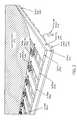
- FIG. 1depicts a diagrammatic view of one embodiment of the invention showing the drive and pickup plate structures with an insulating dielectric layer separating the drive and pickup lines.
- FIG. 2depicts a basic diagrammatic view of one embodiment of the invention showing the basic electrical field operation without an object in close proximity to the drive and pickup plate structures with one drive plate excited by a voltage source.
- FIG. 3depicts a basic diagrammatic view of one embodiment of the invention showing the basic electrical field operation with an object in close proximity to the drive and pickup plate structures with one drive plate excited by a voltage source.
- FIG. 4depicts a basic diagrammatic view of one embodiment of the sensor showing the differences in field intensity with and without an object in close proximity to the drive and pickup plate structures with one drive plate excited by a voltage source.
- FIG. 5depicts a basic diagrammatic view of one embodiment of the invention showing the basic electrical field operation with an object in close proximity of the drive and pickup plate structures with the selected pickup plate amplified and all inactive drive and pickup plates grounded.
- FIG. 6 adepicts a basic diagrammatic view of one embodiment of the invention showing the basic electrical field operation with a finger or object containing a ridge surface feature in close proximity to the active electrode pair.
- FIG. 6 bdepicts a basic diagrammatic view of one embodiment of the invention showing the basic electrical field operation with a finger or object containing a valley surface feature in close proximity to the active electrode pair.
- FIG. 7depicts a diagrammatic view of an x-y grid of plate rows and columns depicted by lumped circuit components that represent the electric field couplings of the sensor at each drive/pickup crossover.
- FIG. 8depicts an example of an embodiment of the placement invention using a differential amplifier to take the signal from the selected pickup plate and subtract it from a reference signal plate for noise reduction purposes.
- FIG. 9 adepicts the drive and sense multiplexing circuitry of an embodiment of the invention which incorporates a tank circuit to compensate for input loading effects.
- FIG. 9 bdepicts the drive and sense multiplexing circuitry of an embodiment of the invention which incorporates cascaded buffers to minimize input loading effects.
- FIG. 9 cdepicts the drive and sense multiplexing circuitry of an embodiment of the invention which incorporates dedicated buffers for each sense to minimize loading effects.
- FIG. 10depicts an embodiment of the invention which incorporates an analog receiver to process the sensed signal, and processing circuitry to perform the drive and sense line scanning function.
- FIG. 11depicts an embodiment of the invention which incorporates a direct digital conversion receiver to process the sensed signal, and processing circuitry to perform the drive and sense line scanning function.
- FIG. 12depicts the layout of the drive and sense traces for an embodiment of the invention which incorporates the folded aspect of the invention laid out flat prior to folding.
- FIG. 13 adepicts the layer stack-up of an embodiment of the invention which incorporates the folding aspect subsequent to folding.
- FIG. 13 bdepicts an embodiment of the invention which incorporates the folding aspect subsequent to folding and assembly into a rigid module.
- FIG. 14depicts a sensor system configured according to the invention for the purpose of sensing features of an object.
- FIG. 15depicts a diagrammatic view of the sensing of a fingerprint features utilizing the invention.
- FIG. 16depicts the process flow steps required to collect a 2-dimensional image with a sensor system configured according to the invention.
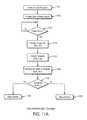
- FIG. 17 adepicts the process flow steps required to authenticate a user with a fingerprint sensor system configured according to the invention.
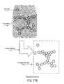
- FIG. 17 bdepicts the process of template extraction from a fingerprint image typically utilized in user authentication applications.
- the inventionprovides a broad solution to shortcomings in the prior art for many applications.
- the inventionis directed to a two-dimensional sensor having sensor lines located on a substrate, such as a flexible substrate for example, that can be folded over on itself to form a grid array with separate sensor lines orthogonal to each other, where the crossover locations of different sensor lines create sensing locations for gathering information of the features and/or characteristics of an object.
- the drive lines and pickup linesare not electrically intersecting or connected in a manner in which they would conduct with each other, they form an impedance sensing electrode pair with a separation that allows the drive lines to project an electrical field hand the pickup lines to receive an electrical field, eliminating the need for distinct electrode structures.
- the two lines crossing with interspersed dielectricintrinsically creates an impedance sensing electrode pair.
- the sensoris configured to activate two one-dimensional sensor lines to obtain one pixel of information that indentifies features and/or characteristics of an object.
- a sensor configured according to the inventionprovides a two dimensional grid that is capable of capturing multiple pixels of information from an object by activating individual pairs of drive and pickup lines and capturing the resultant signal.
- This signalcan be processed with logic or processor circuitry to define features and/or characteristics of an object.
- the informationmay be used to produce renderings of an object, such as a fingerprint, and compare the renderings to secured information for authentication.
- a devicecan utilize the intrinsic impedance sensing electrode pair formed at the crossings between the drive and pickup lines.
- the electric fieldsmay be further focused by grounding drive and pickup lines near or about the area being sensed by the particular crossover location at one time. This prevents interference that may occur if other drive and pickup lines were sensing electric fields simultaneously. More than one electrode pair may be sensed simultaneously. However, where resolution is an important factor, it may be preferred to avoid sensing electrode pairs that are too close to each other to avoid interference and maintain accuracy in sensing object features at a particular resolution.
- intrinsic electrode pairrefers to the use of the impedance sensing electrode pairs that are formed at each of the drive and pickup line crossover locations.
- guard grounds around the pixelare formed dynamically by switching adjacent inactive drive and pickup lines into ground potential. This allows the formation of high density pixel fields with relatively low resolution manufacturing processes, as the minimum pixel pitch for a given process is identical to the minimum feature spacing. This, in turn, enables the use of low cost manufacturing process and materials, which is the key to creating a low cost placement sensor.
- the sensor linesmay consist of drive lines on one layer and pickup lines on another layer, where the layers are located over each other in a manner that allows the separate sensor lines, the drive and pickup lines, to cross over each other to form impedance sensing electrode pairs at each crossover location.
- These crossover locationsprovide individually focused electrical pickup locations or pixels, or electrode pairs where a number of individual data points of features and/or characteristics of an object can be captured.
- the high degree of field focusis due to the small size of the intrinsic electrode pairs, as well as the high density of the neighboring ground provided by the inactive plates.
- the flexible substratemay have a second substrate configured with logic or processor circuitry for sending and receiving signals with the sensor lines to electronically capture information related to the object.
- the utilization of the crossover locations between perpendicular lines on adjacent layers for the pickup cellgreatly reduces the alignment requirements between the layers. Since there are no unique features at a sensor pixel location to align, the only real alignment requirement between the layers is maintaining perpendicularity. If the sense cell locations had specific features, such as the parallel plate features typical of prior art fingerprint sensors, the alignment requirements would include X and Y position tolerance of less than one quarter a pixel size, which would translate to less than +/ ⁇ 12 um in each axis for a 500 DPI resolution fingerprint application.
- a drive lineis activated, with a current source for example, and a pickup line is connected to a receiving circuit, such as an amplifier/buffer circuit, so that the resulting electric field can be captured.
- An electric fieldextends from the drive line to the pickup line through the intermediate dielectric insulating layer. If an object is present, some or all of the electric field may be absorbed by the object, changing the manner in which the electric field is received by the pickup line. This changes the resulting signal that is captured and processed by the pickup line and receiving circuit, and thus is indicative of the presence of an object, and the features and characteristics of the object may be sensed and identified by processing the signal. This processing may be done by some form of logic or processing circuitry.
- the signal driving the drive linemay be a complex signal, may be a varying frequency and/or amplitude, or other signal. This would enable a sensor to analyze the features and/or characteristics of an object from different perspectives utilizing a varying or complex signal.
- the signalmay include simultaneous signals of different frequencies and/or amplitudes that would produce resultant signals that vary in different manners after being partially or fully absorbed by the object, indicating different features and characteristics of the object.
- the signalmay include different tones, signals configured as chirp ramps, and other signals. Processing or logic circuitry may then be used to disseminate various information and data points from the resultant signal.
- the varying or complex signalmay be applied to the drive line, and the pickup line would receive the resulting electric field to be processed.
- Logic or processing circuitrymay be configured to process the resulting signal, such as separating out different frequencies if simultaneous signals are used, so that features and/or characteristics of the object may be obtained from different perspectives.
- each pixelmay be captured in a number of ways.
- a drive linemay be activated, and pickup lines may be turned on and off in a sequence to capture a line of pixels.
- This sequencingmay operate as a scanning sequence.
- a first drive lineis activated by connecting it to a signal source, and then one pickup line is connected to amplifier/buffer circuitry at a time, the information from the pixel formed at the crossing of the two lines is captured, and then disconnected.
- a next pixelis processed in sequence, then another, then another, until the entire array of pickup lines is processed.
- the drive lineis then deactivated, and another drive line is activated, and the pickup lines are again scanned with this active drive line.
- Thesemay be done one at a time in sequence, several non-adjacent pixels may be processed simultaneously, or other variations are possible for a given application. After the grid of pixels is processed, then a rendering of object information will be possible.
- pickup lines or top plates 102 a[m ], 102 b[m+ 1]are located on a insulating dielectric substrate layer 104 and configured to transmit a signal into a surface of an object located in close proximity to the sensor lines.
- Drive lines or bottom plates 106 a[n ], 106 b[n+ 1]are juxtaposed and substantially perpendicular to the drive lines or plates and are located on an opposite side of the a insulating dielectric substrate to form a type of a grid.
- the pickup linesare configured to receive the transmitted electromagnetic fields modified by the impedance characteristics on an object placed within the range of those electric fields.
- FIG. 2a diagrammatic view of a sensor 200 is shown having pickup lines or top plates 202 a , 202 b and insulating layer 204 , and drive lines or bottom plates 206 a , 206 b .
- the Figurefurther illustrates how electromagnetic fields 208 a , 208 b extend between the drive lines and pickup plates through the substrate. Without an object within proximity, the electric field lines are uniform within the sensor structure and between the different lines. When an object is present, a portion of the electric field lines are absorbed by the object and do not return to the pickup plates through the insulating layer.
- an object 310is illustrated proximate the sensor 300 .
- the sensor 300has pickup lines or top plates 302 a , 302 b , an insulating dielectric layer 304 , and drive lines or bottom plates 306 a , 306 b .
- the drive lines and pickup lines of this device examplemay be individually activated, where a drive line/pickup line pair is activated to produce an active circuit.
- the resultis a circuit that transmits electric field from active drive plate 316 into the combined dielectric of the insulating layer 304 and object 310 via electric field lines, 306 a , 306 b , and received by the active pickup plate.
- the sensorcan capture a type of image of the object surface electronically, and generate a representation of the features and characteristics of an object, such as the features and characteristics of a fingerprint in the fingerprint sensor example described below.
- a drive linemay be activated, and the pickup lines may be scanned one or more at a time so that a line of pixels can be captured along the drive line and pickup lines as they are paired along a line at the crossover locations. This is discussed in more detail below in connection with FIG. 5 .
- each area over which a particular drive line overlaps a pickup line with a separation of the a insulating dielectric substrateis an area that can capture and establish a sensing location that defines characteristics or features of a nearby object about that area. Since there exist multiple sensing locations over the area of the sensor grid, multiple data points defining features or characteristics of a nearby object can be captured by the sensor configuration.
- the sensorcan operate as a planar two-dimensional sensor, where objects located on or about the sensor can be detected and their features and characteristics determined.
- a sensor deviceincludes drive lines located on or about an insulating dielectric substrate and configured to transmit a signal onto a surface of an object being sensed.
- Pickup linesare located near or about the drive lines and configured to receive the transmitted signal from the surface of an object.
- the substratemay act as an insulating dielectric or spacing layer.
- the substratemay be for example a flexible polymer based substrate.
- KaptonTM tapeis widely used in flexible circuits such as those used in printer cartridges and other devices.
- the packagemay include such a flexible substrate, where the drive lines may be located on one side of the substrate, and the pickup lines may be located on an opposite side of the substrate.
- the drive linesmay be orthogonal in direction with respect to the pickup lines, and may be substantially perpendicular to the pickup lines.
- a devicemay be configured with drive lines and pickup lines located on or about opposite sides of an insulating dielectric substrate, where the combination of these three components provides capacitive properties.
- the drive linesmay be activated to drive an electric field onto, into or about an object.
- the pickup linescan receive electronic fields that originated from the drive lines, and these electronic fields can be interpreted by processing or logic circuitry to interpret features or characteristics of the object being sensed.
- the layer separating the drive lines from the pickup linescan provide a capacitive property to the assembly.
- a gridmay be formed.
- the drive linesare located and oriented substantially in parallel with respect to each other about a first plane.
- One surface of the substrateis located about the drive lines in a second plane that is substantially parallel relative to the drive lines.
- the pickup linesare located and oriented substantially in parallel with respect to each other about a third plane that is substantially parallel to the first and second planes and also located about another substrate surface that is opposite that of the drive lines, such that the substrate is located substantially between the drive lines and the pickup lines.
- the inventionis directed to a sensor configured with plurality of drive and pickup lines that generally cross over each other at a pixel location and are configured to detect presence and other features and characteristics of a nearby object
- the inventionis not limited to any particular configuration or orientation, but is only limited to the appended claims, their equivalents, and also future claims submitted in this and related applications and their equivalents.
- orientation of the planes(which may be deformable, and thus may be sheets separated by a substantially uniform distance) of groups of components (such as drive lines or pickup lines for example) or substrates may vary in different applications without departing from the spirit and scope of the invention.
- a plurality of drive linesare juxtaposed on one surface of a generally planar substrate, and a plurality of pickup lines are juxtaposed on an opposite surface of the planar substrate.
- the drive linesare substantially orthogonal to the pickup lines, and may be described as substantially perpendicular to the pickup lines.
- the distance between the drive lines and pickup linesmay be filled with a substrate or insulating material that will provide for a capacitive configuration.
- the drive lines on one side of the substrateforms one capacitive plate, and the pickup lines on an opposite side for the corresponding capacitive plate.
- sensor linessuch as sensor drive lines and sensor pickup lines
- substantially parallel drive linesThese drive lines are intended to be described as parallel conductive lines made up of a conductive material formed, etched, deposited or printed onto the surface such as copper, tin, silver and gold.
- conductive linesare seldom “perfect” in nature, and are thus not exactly parallel in practice. Therefore, they are described as “substantially parallel”.
- Different applicationsmay configure some of the drive lines even non-parallel, such that the lines may occur parallel for a portion of the line, and the line may necessarily deviate from parallel in order to connect with other components for the device to operate, or in order to be routed on or about the substrate on which it is formed or traced.
- the separate array of linesmay be described as orthogonal or perpendicular, where the drive lines are substantially orthogonal or perpendicular to the pickup lines.
- the various linesmay not be perfectly perpendicular to each other, and they may be configured to be off-perpendicular or otherwise crossed-over in different angles in particular applications.
- Theyalso may be partially perpendicular, where portions of drive lines may be substantially perpendicular to corresponding portions of pickup lines, and other portions of the different lines may deviate from perpendicular in order to be routed on or about the substrate or to be connected to other components for the device to operate.
- the drive linescan transmit an electromagnetic field toward an object that is proximal to the device.
- the pickup linesmay receive a signal originating from the drive lines and then transmitted through the object and through the substrate and onto the pickup lines.
- the pickup linesmay alternatively receive a signal originating from the drive lines that were then transmitted through the substrate and onto the pickup lines without passing through the object.
- This electric fieldcan vary at different locations on the grid, giving a resultant signal that can be interpreted by some type of logic or processor circuitry to define features and/or characteristics of an object that is proximate the assembly.
- the drive lines and pickup linesmay be controlled by one or more processors to enable the transmission of the signal to an object via the drive lines, to receive a resultant signal from an object via the pickup lines, and to process the resultant signal to define an object image.
- One or more processorsmay be connected in one monolithic component, where the drive lines and pickup lines are incorporated in a package that includes the processor.
- the drive lines, pickup lines and substratemay be assembled in a package by itself, where the package can be connected to a system processor that controls general system functions. This way, the package can be made part of the system by connecting with a system's input/output connections in order to communicate with the system.
- the senorcan be connected as a stand-alone component that communicates with the system processor to perform sensor operations in concert with the system processor.
- a sensormay be configured to drive signals at different frequencies since the impedance of most objects, especially human tissue and organs, will greatly vary with frequency.
- the receiverIn order to measure complex impedance at one or more frequencies of a sensed object, the receiver must be able also to measure phase as well as amplitude.
- the resulting signal generated from a given impedance sensing electrode pairmay result from varying frequencies, known in the art as frequency hoping, where the receiver is designed to track a random, pseudo-random or non-random sequence of frequencies.
- a variation of this embodimentcould be a linear or non-linear frequency sweep known as a chip. In such an embodiment one could measure the impedance of a continuous range frequencies very efficiently.
- a grid sensor as described abovemay be configured to also operate as a pointing device.
- a pointing devicecould perform such functions as well known touch pads, track balls or mice used in desktops and laptop computers.
- a two dimensional impedance sensorthat can measure the ridges and valleys of a finger tip may be configured to track the motion of the fingerprint patterns.
- Prior art swiped fingerprint sensorscan perform this function, but due to the physical asymmetry of the array and the need to speed correct, or “reconstruct” the image in real time make these implementations awkward at best.
- the sensorcould also double as both a fingerprint sensor and a high quality pointing device.
- One device configured according to the inventionincludes a first array of sensor lines on a flexible substrate, and a second array of sensor lines on a flexible substrate, and also a processor configured to process fingerprint data from the first and second arrays of sensor lines.
- the separate sensor linesWhen folded upon itself in the case of a single flexible substrate or when juxtaposed in the case of separate substrates, the separate sensor lines cross each other without electrically shorting to form a grid with cross-over locations that act as pixels from which fingerprint features can be sensed.
- an array of substantially parallel sensor drive linesis located on a surface of the flexible substrate. These drive lines are configured to sequentially transmit signal into a surface of a user's finger activating a line at a time.
- a second array of sensor linesis similar to the first, consisting of substantially parallel sensor pickup lines that are substantially perpendicular to the drive lines. These pickup lines are configured to pick up the signal transmitted from the first.
- the flexible substrateis further configured to be folded onto itself to form a dual layer configuration.
- the first array of sensor drive linesbecomes substantially perpendicular to the second array of pickup sensor lines when the flexible substrate is folded onto itself.
- This folding processcreates crossover locations between these separate arrays of sensor lines—though they must not make direct electrical contact so that they operate independently.
- These crossover locationsrepresent impedance sensing electrode pairs configured to sense pixels of an object and its sub-features juxtaposed relative to a surface of the flexible substrate. The scanning of these pixels is accomplished by activating individual rows and columns sequentially.
- the perpendicular pickup rowsare scanned one at a time over the entire length of the selected driver. Only one row is electrically active (high impedance) at a time, the non active rows are either shorted to ground or multiplexed to a state where they do not cross couple signal.
- a finger ridgeis placed above an array crossover location that is active, it interrupts a portion of the electric field that otherwise would be radiated through the surface film from the active drive column to the selected row pickup.
- the placement of an object's subfeature, such as a ridge or valley in the case of a fingerprint sensor, over an impedance sensing electrode pairresults in a net signal decrease since some of the electric field is conducted to ground through the human body.
- the valleyaffects the radiation of electric field from the selected drive line to the selected pickup line much less than a ridge would.
- this general example of the grid sensorwill be now used to illustrate how such a sensor configured according to the invention can be implemented as a fingerprint sensor, where the object would simply be the surface of the fingerprint on the user's finger.
- This examplewill be carried through the following Figures for illustration of the benefits and novel features of the impedance sensor configured according to the invention.
- any objectmay be sensed by a device configured according to the invention. Again, the example and description are intended only for illustration purposes.
- the senorcan be configured to detect the presence of a finger surface located proximate to the sensor surface, where the drive lines can drive an active electromagnetic field onto the finger surface, and the pickup lines can receive a resulting electromagnetic field signal from the pickup lines.
- the drive linescan generate an electric field that is passed onto the surface of the finger, and the different features of the fingerprint, such as ridges and valleys of the fingerprint surface and possibly human skin characteristics, would cause the resulting signal to change, providing a basis to interpret the signals to produce information related to the fingerprint features.
- a flexible substrateis used as the insulating dielectric layer 104 , to allow for beneficial properties of durability, low cost, and flexibility.
- the drive lines or plates 106 a , 106 bare located on the flexible substrate and configured to transmit a signal into a surface of a user's fingerprint features and structures, such as ridges and valleys, placed on or about the sensor lines.
- the pickup lines 102 a , 102 bare configured to receive the transmitted signal from the user's finger surface.
- a processor(not shown) can be configured to collect and store a fingerprint image based on the received signal from the pickup lines.
- FIG. 4illustrates the field interactions of a basic sensor cell.
- an example a sensor 400configured as an object sensor, where the top plates or pickup lines 402 a , 402 b , . . . , 402 n are located on one side of insulating dielectric layer or substrate 404 .
- Bottom plates or pickup lines 406 a , 406 b , . . . , 406 nare located on an opposite side of the substrate 404 .
- Electric fields 408 a , 408 bextend from bottom plates or drive lines 406 a , 406 b through the insulating layer or substrate 404 and onto active top plate 402 a .
- these drive linesmay be activated one at a time to reduce any interference effects, but the electric field results illustrated here are intended to illustrate a contrast between electric fields that are partially or fully absorbed by the object with electric fields that are not absorbed the object at all.
- This informationmay be collected from drive and pickup plate electrode pairs at each crossover location to sense features and characteristics of the object that is proximate the sensor lines.
- Partially covered top plate or pickup line 402 bis connected to voltmeter 417
- uncovered top plate 402 ais connected to voltmeter 418 .
- Active drive line or bottom plate 406 bis connected is connected to AC signal source 416 , causing an electric field to radiate from active plate 406 b .
- the number of drive lines and pickup linescan vary depending on the application, and it may depend on the cost and resolution desired.
- the electric field lines 408 ais partially captured by the drive lines 402 a and 402 b , and part is captured by the object, in this case finger 410 .
- volt meter 417illustrates the response to the top plate or drive line 402 b
- voltmeter 418illustrates the response of top plate or drive line 402 a .
- the difference in the deflections of voltmeter 417 in comparison 418show the delta in electric field intensity between the two electrode pair locations, one with a finger present the other without.
- FIG. 5another example of a sensor configured according to the invention is illustrated the Drive and pickup configuration when detecting the presence of an object.
- the sensor 500is illustrated, where the top plates or pickup lines 502 a , 502 b , . . . , 502 n are located on one side of insulating layer or substrate 504 , and bottom plates or drive lines 506 a , 506 b , . . . , 506 n are located on an opposite side of the substrate 504 .
- the pickup linesare shown on the layer closest to the object being sensed for maximum sensitivity, and the drive lines shown on the opposite side of the substrate.
- Electric fields 508 a , 508 bextend from bottom plates or drive lines 506 a , 506 b through the insulating layer or substrate 504 and onto active top plate 502 b .
- Other configurationsare possible, perhaps having drive plates on the top, and pickup plates on the bottom.
- the inventionis not limited to any particular configuration that is insubstantially different than the examples and embodiments disclosed and claimed herein.
- FIG. 5further shows a snapshot of one selected individual electrode pair located at the crossover of pickup line 502 b and drive line 506 b , where the remaining pickup and drive lines are not active, shown grounded in FIG. 5 .
- Drive line 506 bis connected to AC voltage source 516
- pickup line 502 bis connected to amplifier/buffer 514 .
- electric field lines 508 a , 508 bare generated, and they radiate from drive line 506 b and are sensed by pickup line 502 b , sending the resultant signal into amplifier/buffer 514 , and are later processed by analog and digital circuit functions.
- Grounding the inactive adjacent drive and pickup linesfocuses the electric fields 508 a and 508 b at the crossover location between the active the drive and pickup plates, limiting crosstalk from adjacent areas on the object being sensed.
- different drive line/pickup line crossover pairingsmay be activated to capture different pixels of information from the object.
- an object sensorit can capture information on the shape of the object, and, if the electrical characteristics are non-uniform across its surface, it's composition.
- the inventionis not limited to this particular configuration, where one single electrode pair, several electrode pairs, or even all electrode pairs may be active at one time for different operations.
- a drive linemay be activated, and the pickup lines may be scanned one or more at a time so that a line of pixels can be captured along the drive line and pickup lines as they are paired along a line at the crossover locations.
- the AC voltage source 516may remain connected to drive line 506 b , and the connection of the amplifier/buffer 516 may cycle or scan over to sequential pickup lines, so that another pixel of information can be captured from another pickup line crossover paired with drive line 506 b .
- drive line 506 bcan be deactivated, than another drive line in sequence can be activated with the AC voltage source, and a new scanning can commence through the pickup lines.
- a two dimensional image or rendering of the object features and characteristicscan be made, such as a rendering of the shape of the object, and potentially a composition map.
- a reduced cost fingerprint swipe sensorcould be configured using the same innovation provided by the invention.
- a reduced number of pickup linescould be configured with a full number of orthogonal drive lines.
- Such a configurationwould create a multi-line swipe sensor that would take the form of pseudo two-dimensional sensor, and when a finger was swiped over it would create a mosaic of partial images or slices. The benefit of this would be to reduce the complexity of image reconstruction task, which is problematic for current non-contact silicon sensors that rely on one full image line and a second partial one to do speed detection.
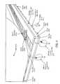
- FIGS. 6 a and 6 billustrate the operation of the sensor when detecting surface features of an object such as fingerprint ridges and valleys.
- the sensoris configured identically to the previous example in FIG. 5 , but in this case is interacting with a textured surface such as a fingerprint.
- FIGS. 6 a and banother example of a sensor configured according to the invention is illustrated.
- the sensor 600is illustrated, where the top plates or pickup lines 602 a - n are located on one side of insulating layer or substrate 604 , and bottom plates or drive lines 606 a - n are located on an opposite side of the substrate 604 .
- For maximum sensitivity pickup linesare shown on the layer closest to the object being sensed, and the drive lines shown on the opposite side of the substrate.
- FIG. 6 ashows electric field lines 620 as they interact with a proximally located object's valley and FIG.
- 6 bshows electric field lines 621 as the interact with a proximally located object's peaks, extending from bottom plate drive line 606 b through the insulating layer or substrate 604 and onto active drive line 606 b .
- the corresponding ridges and valleys over the fingerprint surfacecan be captured by the grid of drive line/pickup line crossover points, and the resulting data can be used to render an image of the fingerprint.
- a stored fingerprintcan then be compared to the captured fingerprint, and they can be compared for authentication. This is accomplished using any one of many fingerprint matching algorithms which are available from vendors as stand alone products. Such vendors include Digital Persona, BioKey, and Cogent Systems, to name just a few.
- FIGS. 6 a and bAlso illustrated in FIGS. 6 a and b , is the individual sensor line pairing of pickup line 602 b and drive line 606 b . Their crossover forms the active electrode pair, and the remaining pickup and drive lines are not active, and will nominally be grounded by electronic switches.
- Drive line 606 bis connected to AC voltage source 616
- pickup line 602 bis connected to amplifier/buffer 605 .
- electric field lines 620 and 621are created as shown in FIGS. 6 a and 6 b respectively, and they emanate between the drive line 606 b and pickup line 602 b , sending a resultant signal that is radiated onto pickup line 602 b and connected to amplifier/buffer 605 , and later processed by analog and digital processing circuitry.
- different drive line/pickup line crossover pairsmay be activated to capture different pixels of information from the object.
- a fingerprintit can capture information on different features and characteristics of the fingerprint and even the body of the finger itself.
- the inventionis not limited to this particular configuration, where one electrode pair, several electrode pairs, or even all electrode pairs may be active at one time for different operations. In practice, it may be preferable for less than all of the electrode pairs to be active at a given time, so that any interference that may occur between close-by pixels would be minimized.
- a drive linemay be activated, and the pickup lines may be scanned one or more at a time so that a line of pixels can be captured along the drive line and pickup lines as they are paired along a line at the crossover points.
- the voltage source 616may remain connected to drive line 606 b , and the connection to buffer/amplifier 605 may cycle or scan over to another pickup line, so that another pixel of information can be captured from another electrode pair using driveline 606 b.
- drive plate 606 bremains excited by AC signal source 616 until an entire column of pixels is scanned, while unused drive plates ( 606 a,c - n etc.), are switched to ground for isolation purposes. Likewise, in one embodiment only one pickup plate is active at a time and some or substantially all other pickup plates are switched to ground to minimize crosstalk.
- the two conductive layers Drive layer 606 and Pickup layer 602are separated by an electrically insulating layer 604 .
- This insulating layer 604has high DC resistance and has a dielectric constant greater than one to allow the transmission of high frequency electric fields through it.
- this layer 602is created by folding a single sided flexible printed circuit board back onto itself. In another embodiment it is created by placing a dielectric layer between two electrically active layers to form a double sided circuit board.
- FIG. 7shows an example of an x-y grid of plate rows and columns depicted by lumped circuit components that represent the electric field couplings of the sensor at each drive/pickup crossover.
- FIG. 7shows a scan snapshot where one drive switch 740 b in the on condition connecting the corresponding plate to the signal source. This activates one entire row 740 b with AC signal over the entire length of the plate which is equal to the sensor width in one dimension.
- each column plate 703 a,b,c etc.will pickup up AC signal through insulating layer 704 and coupling capacitors 761 a,b,c . . . n . Only one pickup plate at a time is active being switched into the buffer amplifier 716 .
- Top Plate 702 bis shown as the active plate in FIG. 7 , while all or substantially all other pickups are shorted to ground via switch matrix 730 a - n , thus the information from one x-y pixel is captured.
- a single rowremains active only as long as it takes the entire number of pickup plates/columns to be scanned.
- Scan time per pixelwill depend on the frequency of operation and the settling time of the detection electronics, but there is no need to scan unduly fast as is typical with prior art swipe sensors.
- prior art swipe sensorsmust scan at a very high pixel rate in order not to lose information due to undersampling relative to the finger speed which can be greater than 20 cm/sec. This reduction in capture speed relative to a swipe sensor relaxes the requirements of the analog electronics and greatly reduces the data rate that a host processor must capture in real time. This not only reduces system cost but allows operation by a host device with much less CPU power and memory. This is critical especially for mobile devices.
- the amount of signal that is coupled into the buffer amplifier 716is a function of how much capacitance is formed by the insulating layer and the finger ridge or valley in close proximity.
- the detailed operation of how these electric fields radiateis shown in FIGS. 6 a and b .
- the total coupling capacitanceis a series combination of the insulating layer capacitance 704 which is fixed for a given thickness, and the variable topological capacitance of the object being sensed. The variable portion of this is shown in FIG. 7 as a series of variable capacitors numbered 760 a - n , 761 a - n , 762 a - n etc., forming a two dimensional array.
- FIG. 8shows an example of an embodiment of the placement sensor using a differential amplifier 880 to take the signal from the selected pickup plate ( 802 a - n ), and subtract it from the reference signal of plate 805 .
- the electrical subtraction of these signalsperforms several functions: first wide band common mode is subtracted out; second, subtracting against reference plate 805 provides a relative reference signal equivalent to an ideal ridge valley; third, common mode carrier signal that couples into both plates other than through a finger is also subtracted out.
- First order carrier cancellation of etch variation in the pickup platesalso occurs when we subtract out carrier that is coupled in by other means than through fingers placed on the sensor. This is critical for high volume manufacturing at a low cost.
- Reference plate 805is intentionally located outside of the finger contact area of the sensor, separated from pickup plates 802 a - n by Gap 885 , Gap 885 is much larger that the nominal gap between the pickup plates which is typically 50 um. In a real world embodiment plate 805 would be positioned under the plastic of a bezel to prevent finger contact, placing it at least 500 um apart from the other pickup plates.
- Each one of the pickup plates 802 a - nis scanned sequentially being switched through pickup switches 830 a - n connecting them to Differential Amplifier 880 .
- the positive leg of the differential amplifierremains connected to reference plate 805 to provide the same signal reference for all of the pickup plates.
- FIG. 9 ashows a circuit diagram of an example of a front end for the placement sensor in a topology that uses a bank of Single Pole Double Throw Switches or SPDTs to scan the pickup plate rows and a bank of Single Pole Single Throw switches to multiplex the pickup plate columns.
- FIG. 9 awe see a snapshot of the analog switches as the scanning process begins. Only the first SPDT switch 1044 a is shown in the “on” position, which allows pickup plate 902 a to conduct its plate signal into Differential Amplifier 980 . The remaining pickup plates are shorted to ground via switches 944 a - 944 n , preventing any pickup signal received by them from entering into differential amplifier 980 .
- Each SPDThas a Parasitic Capacitance 945 , due to the fact that real world switches to not give perfect isolation. In fact the amount of isolation decreases with frequency, typically modeled by a parallel capacitor across the switch poles.
- a SPDT switchwe can shunt this capacitance to ground when an individual plate is not active. Since there is a large array of switches equal to the number of pickup plates, typically 200 for a 500 dpi sensor, the effective shunt capacitance to ground is multiplied by that number. So if a given switch has 0.5 picofarads of parasitic capacitance and there where 200 pickups, that would add up to 100 picofarads of total shunt capacitance.
- a compensating circuitIn order to prevent this large capacitance from diverting most of the received signal from the active pickup to ground, it is desirable in this example to use a compensating circuit. This is accomplished by using resonating inductor 939 , forming a classic bandpass filter circuit in conjunction with parasitic capacitors 945 (one per switch) and tuning capacitors 934 and 937 .
- a two step null & peak tuning calibration procedureis used where tuning capacitor 934 and 937 are individually tuned with inductor 939 using the same drive signal on both the plus and minus inputs to differential amplifier 980 .
- the two bandpass filters formed with inductor 1039 and resonating capacitors 934 , and 937 respectively,will be tuned to the same center frequency when there is zero signal out of differential amplifier 980 .
- capacitors 934 and 937 and inductor 939are tuned together using a differential input signal with opposite 180 degrees phases on the plus and minus inputs to the differential amplifier 980 . They are incremented in lock step until the exact drive carrier frequency is reached, this occurs when the output of differential amplifier 980 is at its peak, making the center frequency equal to the exact frequency of the carrier drive signal 916 .
- a calibration routinewould be performed before each fingerprint scan to minimize drift of this filter with time and temperature.
- the resonating inductor 939needs to have a Q or Quality Factor of at least 10 to give the filter the proper bandwidth characteristics necessary to optimize the signal to noise ratio.
- FIG. 9 bshows an alternate example of a device employing multiple banks of plates grouped together, each with their own differential amplifiers.
- Dividing up the large number of parallel pickup plates into groups each containing a smaller number of platesis an alternate architecture that would not require the use of a tuned bandpass filter in the front end because the parasitic switch capacitances would be greatly reduced. This would have two possible advantages, first lower cost, and second the ability to have a frequency agile front end.
- first switch 944 a of bank 907 ais active. All other switch banks 907 a - 907 n are shown inactive, shorting their respective plates to ground.
- voltage or current differential amplifier 980 ahas any plate signal conducted into it
- voltage or current differential amplifiers 980 b - 980 nhave both their positive and negative inputs shorted to ground through their respective switches 945 a - n and 945 r , preventing any signal from those banks making a contribution to the overall output.
- Each of the differential amplifiers 980 a - 980 nare summed through resistors 987 a - 987 n into summing amplifier 985 . Only the differential amplifier 980 a in this snapshot has plate signal routed into it, so it independently produces signal to the input of summing amplifier 985 . This process is repeated sequentially until all or substantially all of the switch banks 907 a - n , and switch plates 944 a - n , 945 a - n , etc, of the entire array are fully scanned.
- the capacitive input load on each plateis reduced from that of the full array of switches to the number of switches within a given plate group. If we were to divide for example 196 potential pickup plates into 14 banks of 14 plates, resulting in a capacitance load equal to the parasitic capacitance of 14 switches ( 944 ), plus the capacitive load of the differential amplifier. If analog switches 944 are constructed with very low parasitic capacitance then the overall input load would be small enough not to need a bandpass circuit in the front end in order to resonate out the load capacitance. As integrated circuit fabrication techniques improve we would be able design smaller switches with less parasitic capacitance, making this approach become more attractive.
- FIG. 9 cillustrates another example of a front end circuit using individual plate buffers that are multiplexed into a second stage differential amplifier.
- Buffers 98 a through 982 n as illustratedare special buffers that are designed to have very low input capacitance.
- these bufferscould be configured as single stage cascoded amplifiers in order to minimize drain-to-gate Miller capacitance and die area.
- two sets of switchescould be used for each input.
- Analog switches 930 a - 930 nare included in this example to multiplex each selected buffer into differential amplifier 980 .
- Switches 932are included to shut down the power simultaneously to all the other input buffers that are not selected. This effectively puts them at ground potential.
- An alternate embodimentwould be to put input analog switches in front of each amplifier to allow a short of the unused plates directly to ground.
- One effect of this approachmay be an increase in input load capacitance for each plate.
- FIG. 9 cshows a snapshot of the scanning process where top plate 902 a is being sensed though buffer 982 a which has power supplied to it through switch 932 a .
- Analog switch 930 ais closed, routing it to differential amplifier 980 . All other buffer outputs are disconnected from the differential amplifier 980 via analog switches 930 b - n and power switches 982 b - n
- differential amplifier 980The positive input to differential amplifier 980 is always connected to the reference plate 902 r , providing an “air” signal reference to the amp.
- the differential amplifier 980serves to subtract out noise and common mode carrier signal in addition to providing a “air” reference carrier value.
- FIG. 10shows a particular embodiment of a placement sensor implemented with traditional analog receiver technology.
- the analog front endbegins with Differential Amplifier 1080 where selected Pickup Plate 1002 a - n is subtracted from Reference Plate 1005 , which is located outside the finger contact area providing a reference signal equivalent to an ideal finger valley.
- a programmable gain stage or PGA 1090follows the Differential Amplifier 1090 , but could be integrated into the same block providing both gain an subtraction in a single stage.
- PGA 1090is designed to have a gain range wide enough to compensate for production variations in plate etching and solder mask thickness between the layers.
- Control processor 1030orchestrates the scanning of the two dimensional sensor plate array.
- Drive plates/columns 100 a - 1002 nare scanned sequentially by the Drive Plate Scanning Logic 1040 in the Control Processor 1030 .
- a selected drive plateis activated it is connected to carrier signal source 1016 .
- All inactive drive platesare connected to ground.
- the active drive plateremains on long enough for the entire row of Pickup Plates 1002 a - n to be scanned by Pickup Plate Logic 1045 .
- Analog mixer 1074multiplies the gained up plate signal against the reference carrier 1013 .
- the resultis a classic spectrum of base band plus harmonic products at multiples of the carrier frequency.
- An analog low pass filter 1025is employed to filter out the unwanted harmonics and must have a sharp enough roll of to attenuate the information associated with of the second harmonic without loosing base band information.
- A/D Converter 1074Following the low pass filter is an A/D Converter 1074 that must sample at a least twice the pixel rate to satisfy the Nyquist criteria.
- Memory buffer 1032stores the A/D samples locally with sufficient size to keep up with the worst case latency of the host controller.
- the A/D Sample Control Line 1078provides a sample clock for the converter to acquire the sequential pixel information that is created by the sequencing of the plate rows and columns.
- FIG. 11shows an example of one embodiment of a placement sensor implemented with direct digital conversion receiver technology.
- the analog front endbegins with Differential Amplifier 1180 where selected Pickup Plate 1102 a - n is subtracted from Reference Plate 1105 , which is located outside the finger contact area providing a reference signal equivalent to an ideal finger valley.
- the electrical subtraction of these signalsperforms several functions: first wide band common mode is subtracted out; second, subtracting against reference plate 1105 provides a relative reference signal equivalent to an ideal ridge valley; third, common mode carrier signal that couples into both plates other than through a finger is also subtracted out. Elimination of common mode is particularly important in high RF noise environments. First order carrier cancellation of etch variation in the pickup plates also occurs when we subtract out carrier that is coupled in by other means than through fingers placed on the sensor. This is critical for high volume manufacturing at a low cost.
- a programmable gain stage or PGA 1190follows the Differential Amplifier, which could easily be combined into a single differential amplifier including programmable gain as is commonly done in modern integrated circuit design PGA 1190 is designed to have a gain range wide enough to compensate for production variations in plate etching and solder mask thickness between the layers.
- Control processor 1130orchestrates the scanning of the two dimensional sensor plate array.
- Drive plates/columns 110 a - 1102 nare scanned sequentially by the Drive Plate Scanning Logic 1140 in the Control Processor 1130 .
- a selected drive plateis activated it is connected to carrier signal source 1116 .
- All inactive drive platesare connected to ground.
- the active drive plateremains on long enough for the entire row of Pickup Plates 1102 a - n to scanned by Pickup Plate Logic 1145 and captured by the A/D converter 1125 .
- the A/D Converter 1125is sampled at a rate of at least twice the carrier frequency to satisfy the Nyquist criteria.
- the A/D Sample Control Line 1107provides a sample clock for the converter to acquire the sequential pixel information that is created by the sequencing of the plate rows and columns.
- a Digital Mixer 1118that digitally multiplies the A/D output which is at the carrier frequency against the reference carrier generated by the Digitally Controlled Oscillator 1110 .
- the resultis that the signal is down converted to the base band with the carrier removed.
- a combination decimator and digital filter 1120follows the Digital Mixer 1118 .
- This blockperforms sampling down conversion, reducing the sample rate from at least twice the carrier frequency to at least twice the pixel rate which is much lower.
- the digital filterwould typically include a Cascaded Integrator Comb, or CIC filter, which removes the unwanted spectral byproducts of mixing as well as improving the receiver signal to noise.
- a CIC filterprovides a highly efficient way to create a narrow passband filter after mixing the signal down to baseband with the digital mixer.
- the CIC filtermay be followed by a FIR filter running at the slower decimated rate to correct passband droop.
- Control Processor Buffer1132
- a relatively small Control Processor Buffer1132
- a swipe sensorwhich must scan the partial image frames at a rate fast enough to keep up with the fastest allowable swipe speed, usually around 200 ms.
- a slow swipe of two secondsmust also be accommodated, requiring ten times the amount of memory as the fastest one.
- Various techniqueshave been developed to throw away redundant sample lines before storage, but even with that the real time storage requirements are much greater for swipe sensors. This is a critical factor in Match on Chip applications where memory capacity is limited.
- a placement sensorhas no real-time data acquisition or processing requirements on the host processor beyond the patience of the user for holding their finger in place.
- Chip on Flexis a configuration where a processor chip is attached to a flexible substrate, such as KaptonTM tape, and that is electrically connected to conductive lines and possibly other components located on the flexible substrate.
- the example shownillustrates an integrated circuit 1210 , which may be a logic circuit formed on a silicon substrate, a microprocessor, or other circuit for processing pixel information captured from a sensor circuit.
- integrated circuit 1210may be a mixed signal chip that enables all or some of the functions described in FIG. 16 below. In one embodiment, it has enough inputs and outputs to drive a 200 by 200 line array of drive and pickup lines, and may have more or less of either lines.
- the top layer 1220is formed by an array of pickup lines connected directly to integrated circuit 1210 . This may be a flip chip mounted directly to the flex substrate without bond wires.
- the bottom layeris formed by folding the single layer back onto itself along the folding axis 1230 to create double layer active sensor area 1255 . The drive lines fold to create the bottom layer 1225 .
- the drive lines in this exampleare split into left and right groups 1240 and 1242 respectively for the sake of layout balance, but could be all on the left or right side of the sensing area.
- the left drive plate bundles 1240 , and right drive plate bundles 1242are inter-digitated with alternating left and right feeds to form a continuous line array on bottom layer 1225 .
- Flexible substrate based connector 1235routes power, ground and interface signals out to an external host or onto another substrate that contains system level components, such as those illustrated in FIG. 16 and described below. These components may include but are not limited to a processor with memory, logic enabling imbedded matching algorithm(s) and encrypting/decrypting functions.
- connector 1235may be attached to the host substrate using conductive adhesive otherwise known as anisotropic conductive film (ACF attach), which may be labeled as “high density” in some products.
- ACF attachanisotropic conductive film
- the flex layer structure 1300includes an imaging area 1350 , in which drive lines form crossover locations with pickup lines, where the crossover locations are formed by folding the top layer 1370 over bottom layer 1372 , folding the flexible substrate upon itself about flex bend radius 1374 .
- the top flex 1364is layered over top soldermask 1362 , which is layered upon top copper or pickup lines 1360 .
- Bottom layer solder mask 1370is folded under top copper 1360
- bottom copper 1372is formed under solder mask 1370 and over bottom flex 1375 .
- FIG. 13 ban example of a module structure 1301 is shown for mounting the flex layer structure 1300 of FIG. 13 a .
- the example structure 1301includes rigid substrate 1330 that receives the flex top layer 1370 on its top layer with flex locating pins or plastic frame 1337 configured to ensure alignment of the drive plates with the pickup plates.
- the x-y alignment tolerance requirementsmay be on the order of several pixels, rather than the sub-pixel alignment tolerances that would be required if there were features to be matched between the two layers.
- the four mounting holes ( 1337 ) on each layerare sufficient to ensure angular and x-y alignment. Also illustrated is driver chip 1310 and imaging area 1350 .
- a sensor devicemay be incorporated into a system, or may be configured as a stand-alone product.
- the sensor componentsmay be encased in a housing (not shown), and electrical connections exposed for connection to a device or system that would utilize such a device.
- a housingnot shown
- electrical connections exposed for connection to a device or system that would utilize such a deviceThose skilled in the art will immediately see how a sensor configured according to the invention as described herein can be incorporated into a housings that are widely used in different industry sectors.
- the mechanical connections, designs and structuresmay necessarily vary according to a particular application.
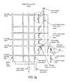
- FIG. 14illustrates a diagrammatic representation of a system 1400 that incorporates a sensor 1402 configured according to the invention with the folded flexible or rigid substrate 1404 having a top layer 1406 and a bottom layer 1408 , and each having either pickup lines or plates and drive lines or plates respectively depending on the application, though not shown here.
- the two-dimensional sensing area 1411is shown with an object 1410 on top, which may be a finger in the case of a fingerprint sensor, or another object in another application.
- the top layer's pickup plates or lines(not shown) communicate with top plate processing circuitry 1410 via communication link 1412 to send resultant signals received.
- Drive lines or platesare located but not shown here on bottom layer 1408 , and receive drive signals from bottom plate processing circuitry 1414 via communication line 1416 .
- the top plate processing circuitry 1410includes front end buffers and amplifiers 1416 configured to receive, amplify and/or buffer or store a resultant signal received from the pickup plates or lines.
- a switch array 1418such as that illustrated in FIG.
- DSPdigital signal processor
- Bottom plate processing circuitry 1414is configured to produce a drive signal for use by drive plates or lines located on the bottom layer 1408 of the sensor substrate 1404 , and includes drivers and scanning logic 1424 for producing the signal, and programmable frequency generate 1426 for programmable setting the frequency in which the drive signal is set.
- the bottom plate processing circuitry 1414includes communication link 1428 , likewise, top plate circuitry has communication link 1420 for communicating with system buss 1432 for sending and receiving communications among the system, such as to processors, memory modules, and other components.
- System buss 1432communicates with persistent memory 1434 via communication link 1436 for storing algorithms 1428 , application software 1440 , templates 1442 , and other code for persistent and frequent use by processor 1444 .
- Processor 1444includes processor logic having logic and other circuitry for processing signals received from the system buss and originating from the sensor 1402 , and also includes arithmetic logic unit 1450 configured with logical circuits for performing basic and complex arithmetic operations in conjunction with the processor.
- Processor memory 1452is configured for local storage for the processor 1444 , for example for storing results of calculations and retrieval for further calculations.
- drive signalsare controlled by processor 1444 , and parameters for the drive signals originating from bottom plate processing circuitry 1414 are set in the bottom plate processing circuitry 1414 by the processor 1444 .
- Drive signalsare generated by logic 1424 within the parameters set in generator 1426 and sent to bottom plate 1408 via communication link 1416 .
- These signalsgenerate electromagnetic fields that extend to pickup lines on top layer 1406 about the sensing area 1411 .
- These signalsare cycled through different pixel electrode pairs on the sensor grid (not shown here, but described above.), and some of these electromagnetic fields are absorbed by the object 1410 (such as a fingerprint for example).
- the resultant signalis picked up by the pickup plates or lines located on top layer 1406 about the sensing area (not shown here, but described above.).
- the resultant signalis then transmitted to top plate processing circuitry 1410 via communication line 1412 , and the signal is processed and transmitted to storage or processor 1444 for further processing.
- data related to features and characteristics of the objectcan be defined and utilized by the system.
- the imagemay be a fingerprint image that can be compared to a stored fingerprint image, and, if there is a match, it can be used to validate a user.
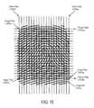
- FIG. 15Illustrates how a device configured according to the invention may be applied to a fingerprint sensing application.
- a userplaces a finger with fingerprint ( 1510 ) over the sensor grid, which is formed by the crossover locations of the drive plates ( 1506 a - 1506 n ) and the pickup plates ( 1502 a - 1502 m ).
- Image pixel 1561 asenses the fingerprint area above the electrode pair of drive plate 1506 a and pickup plate 1502 a
- pixel 1561 asenses the crossover of drive 1506 n and pickup 1502 a
- pixel 1562 nsenses the area above the crossover of drive 1506 n and pickup 1502 m
- FIG. 16illustrates the steps required to collect the fingerprint image as shown in FIG. 15 , using the embodiment of the invention shown in FIGS. 11 and 14 .
- Image capturebegins at step 1601 .
- a row counteris initialized to 1 at step 1602 .
- Step 1603is the beginning of a row scan sequence.
- a column counteris set to 1 at step 1603 .
- the top plate scanning logic 1145activates the appropriate analog switch (one of 1103 a through 1103 n ) for the selected row.
- Step 1605the sense of an individual pixel begins when the bottom plate scanning logic 1140 activates the appropriate drive plate (one of 1106 a through 1106 n ) with the carrier signal 1116 .
- step 1606the signal from differential amplifier 1180 is sampled repeatedly by A/D converter 1125 after processing through programmable gain amplifier 1190 .
- Digital mixer 1118mixes the samples down to the baseband frequency set by digital oscillator 1110 .
- the baseband signalis then filtered by digital decimating filter 1120 to produce a signal level value for the current pixel.
- the functions performed for this step in the embodiment of FIG. 11could alternatively be performed by the corresponding analog receiver shown in FIG. 10 , or other functionally similar arrangements.
- step 1607the signal level value derived in step 1606 is stored in the appropriate position in memory buffer 1132 which corresponds to the currently selected row and column.
- step 1608the column number is incremented, and in step 1609 the column number is tested to determine whether the current row collection has been completed. If the row has not been completed, we return to step 1605 to collect the next pixel in the row. If the row is complete, we proceed to step 1610 and increment the row number. In step 1611 , we test the row number to determine if all the rows have been scanned. If not, flow returns to 1603 to start the next row back at the first column. Once all the rows have been scanned, image capture is complete, and we proceed to step 1612 , at which point the image is ready for further processing or transfer to long term storage.
- row and column scanning ordermay not correspond directly to physical position in the array, as some implementations may more optimally be sampled in interleaved fashions.
- FIG. 17an example of the example as shown in FIG. 14 in a user authentication application.
- a system level application 1440 on processor 1444requires user authentication.
- the useris prompted to provide a finger for verification.
- the systemwaits for finger presence to be detected in step 1703 . This can be performed by collecting a reduced size image as described in FIG. 16 and testing for finger image, or via other dedicated hardware. Once finger presence is detected, a complete image is collected in step 1704 , using the method described in FIG. 16 or other substantially similar method. This image is then stored and in step 1705 converted into a template 1712 as shown in FIG.
- step 1707the template is then compared against one or more enrollment templates that were retrieved from persistent template storage 1142 in step 1706 . If a match is found, the user is authenticated in step 1708 and granted access to the application. If no match is found, the user is rejected in step 1709 , and access is denied.
- the inventionhas application in many areas, particularly in biometric sensors. Fingerprint sensors, for example, and other biometric sensors are gaining increasing acceptance for use in a wide variety of applications for security and convenience reasons. Devices, systems and methods configured according to the invention will have improved security of the biometric verification process without increasing the cost of the system. Furthermore, the invention may extend to devices, systems and methods that would benefit from validation of components. As discussed above, the invention includes the ability for the host and sensor to include any combination or subset of the above components, which may be arranged and configured in the manner most appropriate for the system's intended application. Those skilled in the art will understand that different combinations and permutations of the components described herein are possible within the spirit and scope of the invention, which is defined by the appended Claims, their equivalents, and also Claims presented in related applications in the future and their equivalents.
- the inventionmay also involve a number of functions to be performed by a computer processor, such as a microprocessor.
- the microprocessormay be a specialized or dedicated microprocessor that is configured to perform particular tasks according to the invention, by executing machine-readable software code that defines the particular tasks embodied by the invention.
- the microprocessormay also be configured to operate and communicate with other devices such as direct memory access modules, memory storage devices, Internet related hardware, and other devices that relate to the transmission of data in accordance with the invention.
- the software codemay be configured using software formats such as Java, C++, XML (Extensible Mark-up Language) and other languages that may be used to define functions that relate to operations of devices required to carry out the functional operations related to the invention.
- the codemay be written in different forms and styles, many of which are known to those skilled in the art. Different code formats, code configurations, styles and forms of software programs and other means of configuring code to define the operations of a microprocessor in accordance with the invention will not depart from the spirit and scope of the invention.
- Cache memory devicesare often included in such computers for use by the central processing unit as a convenient storage location for information that is frequently stored and retrieved.
- a persistent memoryis also frequently used with such computers for maintaining information that is frequently retrieved by the central processing unit, but that is not often altered within the persistent memory, unlike the cache memory.
- Main memoryis also usually included for storing and retrieving larger amounts of information such as data and software applications configured to perform functions according to the invention when executed by the central processing unit.
- RAMrandom access memory
- SRAMstatic random access memory
- DRAMdynamic random access memory
- flash memoryand other memory storage devices that may be accessed by a central processing unit to store and retrieve information.
- RAMrandom access memory
- SRAMstatic random access memory
- DRAMdynamic random access memory
- flash memoryand other memory storage devices that may be accessed by a central processing unit to store and retrieve information.
- RAMrandom access memory
- SRAMstatic random access memory
- DRAMdynamic random access memory
- flash memoryand other memory storage devices that may be accessed by a central processing unit to store and retrieve information.
- RAMrandom access memory
- SRAMstatic random access memory
- DRAMdynamic random access memory
- flash memoryand other memory storage devices that may be accessed by a central processing unit to store and retrieve information.
- RAMrandom access memory
- SRAMstatic random access memory
- DRAMdynamic random access memory
- machine-readable mediumshould be taken to include a single medium or multiple media (e.g., a centralized or distributed database, and/or associated caches and servers) that store the one or more sets of instructions.
- the term “machine-readable medium”shall also be taken to include any medium that is capable of storing, encoding or carrying a set of instructions for execution by the machine and that causes the machine to perform any one or more of the methodologies of the present invention.
- the machine-readable mediumincludes any mechanism that provides (i.e., stores and/or transmits) information in a form readable by a machine (e.g., a computer, PDA, cellular telephone, etc.).
- a machine-readable mediumincludes memory (such as described above); magnetic disk storage media; optical storage media; flash memory devices; biological electrical, mechanical systems; electrical, optical, acoustical or other form of propagated signals (e.g., carrier waves, infrared signals, digital signals, etc.).
- the device or machine-readable mediummay include a micro-electromechanical system (MEMS), nanotechnology devices, organic, holographic, solid-state memory device and/or a rotating magnetic or optical disk.
- MEMSmicro-electromechanical system
- the device or machine-readable mediummay be distributed when partitions of instructions have been separated into different machines, such as across an interconnection of computers or as different virtual machines.
- references in the specification to “an embodiment,” “one embodiment,” “some embodiments,” or “other embodiments”means that a particular feature, structure, or characteristic described in connection with the embodiments is included in at least some embodiments, but not necessarily all embodiments.
- the various appearances “an embodiment,” “one embodiment,” or “some embodiments”are not necessarily all referring to the same embodiments. If the specification states a component, feature, structure, or characteristic “may”, “might”, or “could” be included, that particular component, feature, structure, or characteristic is not required to be included. If the specification or Claim refers to “a” or “an” element, that does not mean there is only one of the element. If the specification or Claims refer to “an additional” element, that does not preclude there being more than one of the additional element.
- the methods, systems and devicesinclude improved security operations and configurations with a novel approach to biometric systems. Such systems would greatly benefit from increased security features, particularly in financial transactions.
- this embodimentis described and illustrated in the context of devices, systems and related methods of validating biometric devices such as fingerprint sensors, the scope of the invention extends to other applications where such functions are useful.
- biometric devicessuch as fingerprint sensors
- the scope of the inventionextends to other applications where such functions are useful.
- the foregoing descriptionhas been with reference to particular embodiments of the invention, it will be appreciated that these are only illustrative of the invention and that changes may be made to those embodiments without departing from the principles of the invention, the scope of which is defined by the appended Claims and their equivalents.
Landscapes
- Engineering & Computer Science (AREA)
- Human Computer Interaction (AREA)
- Physics & Mathematics (AREA)
- General Physics & Mathematics (AREA)
- Multimedia (AREA)
- Theoretical Computer Science (AREA)
- Image Input (AREA)
- Measurement Of Length, Angles, Or The Like Using Electric Or Magnetic Means (AREA)
- Measurement Of The Respiration, Hearing Ability, Form, And Blood Characteristics Of Living Organisms (AREA)
Abstract
Description
Claims (30)
Priority Applications (21)
| Application Number | Priority Date | Filing Date | Title |
|---|---|---|---|
| US12/688,790US8421890B2 (en) | 2010-01-15 | 2010-01-15 | Electronic imager using an impedance sensor grid array and method of making |
| US12/820,100US8791792B2 (en) | 2010-01-15 | 2010-06-21 | Electronic imager using an impedance sensor grid array mounted on or about a switch and method of making |
| EP11733400.3AEP2524339B1 (en) | 2010-01-15 | 2011-01-13 | Fingerprint sensing system with a switch underlying a fingerprint sensor array or embedded within layers of the fingerprint sensor array |
| CN201710403900.4ACN107220626B (en) | 2010-01-15 | 2011-01-13 | Electronic imager using an impedance sensor grid array |
| JP2012549092AJP5886211B2 (en) | 2010-01-15 | 2011-01-13 | Electronic imaging device using impedance sensor grid array mounted on or around the switch |
| KR1020127021318AKR101769640B1 (en) | 2010-01-15 | 2011-01-13 | Electronic Imager Using an Impedance Sensor Grid Array and Method of Making |
| JP2012549090AJP6012474B2 (en) | 2010-01-15 | 2011-01-13 | Electronic imaging apparatus using impedance sensor grid array and manufacturing method thereof |
| PCT/US2011/021196WO2011088252A1 (en) | 2010-01-15 | 2011-01-13 | Electronic imager using an impedance sensor grid array mounted on or about a switch |
| KR1020127021324AKR101839159B1 (en) | 2010-01-15 | 2011-01-13 | Electronic imager using an impedance sensor grid array mounted on or about a switch |
| CN201180014237.XACN102893248B (en) | 2010-01-15 | 2011-01-13 | Use electronic imager and the manufacture method of impedance transducer grid array |
| PCT/US2011/021192WO2011088248A1 (en) | 2010-01-15 | 2011-01-13 | Electronic imager using an impedance sensor grid array and method of making |
| CN201180014263.2ACN102906761B (en) | 2010-01-15 | 2011-01-13 | Electronic imager using a grid array of impedance sensors mounted on or around the switch |
| TW100101375ATWI502518B (en) | 2010-01-15 | 2011-01-14 | Electronic imager using an impedance sensor grid array and method of making |
| TW100101376ATWI553564B (en) | 2010-01-15 | 2011-01-14 | Fingerprint sensing system using a switch embedded withn a layered fingerprint sensor and mounting system thereof |
| US13/118,243US8866347B2 (en) | 2010-01-15 | 2011-05-27 | Biometric image sensing |
| US13/620,271US9268988B2 (en) | 2010-01-15 | 2012-09-14 | Biometric image sensing |
| US13/801,991US9600704B2 (en) | 2010-01-15 | 2013-03-13 | Electronic imager using an impedance sensor grid array and method of making |
| US14/946,040US9659208B2 (en) | 2010-01-15 | 2015-11-19 | Biometric image sensing |
| US15/496,161US10115001B2 (en) | 2010-01-15 | 2017-04-25 | Biometric image sensing |
| US16/149,872US10592719B2 (en) | 2010-01-15 | 2018-10-02 | Biometric image sensing |
| US16/797,753US11080504B2 (en) | 2010-01-15 | 2020-02-21 | Biometric image sensing |
Applications Claiming Priority (1)
| Application Number | Priority Date | Filing Date | Title |
|---|---|---|---|
| US12/688,790US8421890B2 (en) | 2010-01-15 | 2010-01-15 | Electronic imager using an impedance sensor grid array and method of making |
Related Child Applications (2)
| Application Number | Title | Priority Date | Filing Date |
|---|---|---|---|
| US12/820,100Continuation-In-PartUS8791792B2 (en) | 2010-01-15 | 2010-06-21 | Electronic imager using an impedance sensor grid array mounted on or about a switch and method of making |
| US13/801,991ContinuationUS9600704B2 (en) | 2010-01-15 | 2013-03-13 | Electronic imager using an impedance sensor grid array and method of making |
Publications (2)
| Publication Number | Publication Date |
|---|---|
| US20110176037A1 US20110176037A1 (en) | 2011-07-21 |
| US8421890B2true US8421890B2 (en) | 2013-04-16 |
Family
ID=44277363
Family Applications (2)
| Application Number | Title | Priority Date | Filing Date |
|---|---|---|---|
| US12/688,790Active2031-01-01US8421890B2 (en) | 2010-01-15 | 2010-01-15 | Electronic imager using an impedance sensor grid array and method of making |
| US13/801,991Active2030-11-30US9600704B2 (en) | 2010-01-15 | 2013-03-13 | Electronic imager using an impedance sensor grid array and method of making |
Family Applications After (1)
| Application Number | Title | Priority Date | Filing Date |
|---|---|---|---|
| US13/801,991Active2030-11-30US9600704B2 (en) | 2010-01-15 | 2013-03-13 | Electronic imager using an impedance sensor grid array and method of making |
Country Status (2)
| Country | Link |
|---|---|
| US (2) | US8421890B2 (en) |
| TW (1) | TWI502518B (en) |
Cited By (37)
| Publication number | Priority date | Publication date | Assignee | Title |
|---|---|---|---|---|
| US20110267284A1 (en)* | 2010-05-03 | 2011-11-03 | Hsin-Hao Lee | Touch-controlled electronic apparatus and related assembly method |
| US20120134549A1 (en)* | 2010-01-15 | 2012-05-31 | Picofield Technologies Inc. | Biometric Image Sensing |
| US20130141118A1 (en)* | 2011-12-01 | 2013-06-06 | David Brent GUARD | Capacitive Coupling of Bond Pads |
| US8811688B2 (en) | 2004-04-16 | 2014-08-19 | Synaptics Incorporated | Method and apparatus for fingerprint image reconstruction |
| US20150036897A1 (en)* | 2004-10-04 | 2015-02-05 | Synaptics Incorporated | Fingerprint sensing assemblies and methods of making |
| WO2015127046A1 (en) | 2014-02-21 | 2015-08-27 | Idex Asa | Sensor employing overlapping grid lines and conductive probes for extending a sensing surface from the grid lines |
| US9158958B2 (en) | 2010-10-28 | 2015-10-13 | Synaptics Incorporated | Signal strength enhancement in a biometric sensor array |
| WO2016103215A1 (en) | 2014-12-24 | 2016-06-30 | Idex Asa | Fingerprint sensor employing an integrated noise rejection structure |
| US9400914B2 (en)* | 2014-10-24 | 2016-07-26 | Egis Technology Inc. | Method and electronic device for generating fingerprint enrollment data |
| US20160225209A1 (en)* | 2010-07-19 | 2016-08-04 | Risst Ltd. | Fingerprint sensors and systems incorporating fingerprint sensors |
| USD771050S1 (en)* | 2015-09-21 | 2016-11-08 | JENETRIC GmbH | Fingerprint scanner with graphical display |
| US9501685B2 (en) | 2013-02-22 | 2016-11-22 | Idex Asa | Integrated finger print sensor |
| WO2016207819A1 (en) | 2015-06-23 | 2016-12-29 | Idex Asa | Double-sided fingerprint sensor |
| US20170024602A1 (en)* | 2015-07-20 | 2017-01-26 | Lg Display Co., Ltd. | Fingerprint sensor integrated type touch screen device |
| WO2017085669A3 (en)* | 2015-11-20 | 2017-06-29 | Idex Asa | Electronic sensor supported on rigid substrate |
| US9740326B2 (en) | 2015-03-31 | 2017-08-22 | Synaptics Incorporated | Sensor array with split-drive differential sensing |
| US9817506B2 (en) | 2015-03-31 | 2017-11-14 | Synaptics Incorporated | Sensor array configurations for differential readout |
| US9823794B2 (en) | 2015-03-31 | 2017-11-21 | Synaptics Incorporated | Differential readout for sensor array |
| WO2018138651A1 (en) | 2017-01-24 | 2018-08-02 | Idex Asa | Configurable, encapsulated sensor module and method for making same |
| WO2018172978A1 (en) | 2017-03-23 | 2018-09-27 | Idex Asa | Sensor array system selectively configurable as a fingerprint sensor or data entry device |
| US10203816B2 (en) | 2013-05-07 | 2019-02-12 | Egis Technology Inc. | Apparatus and method for TFT fingerprint sensor |
| WO2019058259A1 (en) | 2017-09-19 | 2019-03-28 | Idex Asa | Double sided sensor module suitable for integration into electronic devices |
| WO2019116233A1 (en) | 2017-12-12 | 2019-06-20 | Idex Asa | Power source for biometric enrollment with status indicators |
| WO2019138302A1 (en) | 2018-01-12 | 2019-07-18 | Idex Asa | Systems and methods for noise reduction in sensors |
| WO2020039389A2 (en) | 2018-08-22 | 2020-02-27 | Idex Biometrics Asa | Systems and methods for improving image quality in sensors |
| US10620727B2 (en) | 2014-07-24 | 2020-04-14 | Beijing Lenovo Software Ltd. | Information processing method and electronic device |
| US10692991B2 (en) | 2018-09-06 | 2020-06-23 | Globalfoundries Inc. | Gate-all-around field effect transistors with air-gap inner spacers and methods |
| WO2020144652A1 (en) | 2019-01-11 | 2020-07-16 | Idex Biometrics Asa | Systems and methods for accelerating data capture in sensors |
| US10903317B1 (en) | 2019-08-07 | 2021-01-26 | Globalfoundries U.S. Inc. | Gate-all-around field effect transistors with robust inner spacers and methods |
| US10928180B2 (en)* | 2017-04-22 | 2021-02-23 | Tactual Labs Co. | Flexible deformation sensor |
| US11106310B2 (en) | 2019-08-22 | 2021-08-31 | Idex Biometrics Asa | Systems and methods for improving image quality in sensors |
| US11250307B2 (en) | 2017-03-23 | 2022-02-15 | Idex Biometrics Asa | Secure, remote biometric enrollment |
| WO2023281006A1 (en) | 2021-07-08 | 2023-01-12 | Idex Biometrics Asa | Integrated systems including a sensor and a display |
| WO2023046932A1 (en) | 2021-09-24 | 2023-03-30 | Idex Biometrics Asa | Improved flexible inlay and manufacturing method thereof |
| WO2023131609A1 (en) | 2022-01-04 | 2023-07-13 | Idex Biometrics Asa | Antenna extender |
| EP4352680A1 (en) | 2021-05-20 | 2024-04-17 | Idex Biometrics Asa | Transaction authorization using biometric identity verification |
| US12094972B2 (en) | 2019-05-08 | 2024-09-17 | Globalfoundries U.S. Inc. | Gate-all-around field effect transistors having end portions of nanosheet channel layers adjacent to source/drain regions being wider than the center portions |
Families Citing this family (74)
| Publication number | Priority date | Publication date | Assignee | Title |
|---|---|---|---|---|
| US8447077B2 (en) | 2006-09-11 | 2013-05-21 | Validity Sensors, Inc. | Method and apparatus for fingerprint motion tracking using an in-line array |
| US8116540B2 (en) | 2008-04-04 | 2012-02-14 | Validity Sensors, Inc. | Apparatus and method for reducing noise in fingerprint sensing circuits |
| US10702326B2 (en) | 2011-07-15 | 2020-07-07 | Virginia Tech Intellectual Properties, Inc. | Device and method for electroporation based treatment of stenosis of a tubular body part |
| US9198733B2 (en) | 2008-04-29 | 2015-12-01 | Virginia Tech Intellectual Properties, Inc. | Treatment planning for electroporation-based therapies |
| US9867652B2 (en) | 2008-04-29 | 2018-01-16 | Virginia Tech Intellectual Properties, Inc. | Irreversible electroporation using tissue vasculature to treat aberrant cell masses or create tissue scaffolds |
| US10245098B2 (en) | 2008-04-29 | 2019-04-02 | Virginia Tech Intellectual Properties, Inc. | Acute blood-brain barrier disruption using electrical energy based therapy |
| US11272979B2 (en) | 2008-04-29 | 2022-03-15 | Virginia Tech Intellectual Properties, Inc. | System and method for estimating tissue heating of a target ablation zone for electrical-energy based therapies |
| US9283051B2 (en) | 2008-04-29 | 2016-03-15 | Virginia Tech Intellectual Properties, Inc. | System and method for estimating a treatment volume for administering electrical-energy based therapies |
| US10238447B2 (en) | 2008-04-29 | 2019-03-26 | Virginia Tech Intellectual Properties, Inc. | System and method for ablating a tissue site by electroporation with real-time monitoring of treatment progress |
| US11254926B2 (en) | 2008-04-29 | 2022-02-22 | Virginia Tech Intellectual Properties, Inc. | Devices and methods for high frequency electroporation |
| US8992517B2 (en) | 2008-04-29 | 2015-03-31 | Virginia Tech Intellectual Properties Inc. | Irreversible electroporation to treat aberrant cell masses |
| US8698594B2 (en) | 2008-07-22 | 2014-04-15 | Synaptics Incorporated | System, device and method for securing a user device component by authenticating the user of a biometric sensor by performance of a replication of a portion of an authentication process performed at a remote computing device |
| US8391568B2 (en) | 2008-11-10 | 2013-03-05 | Validity Sensors, Inc. | System and method for improved scanning of fingerprint edges |
| US8278946B2 (en) | 2009-01-15 | 2012-10-02 | Validity Sensors, Inc. | Apparatus and method for detecting finger activity on a fingerprint sensor |
| US8600122B2 (en) | 2009-01-15 | 2013-12-03 | Validity Sensors, Inc. | Apparatus and method for culling substantially redundant data in fingerprint sensing circuits |
| US8632534B2 (en) | 2009-04-03 | 2014-01-21 | Angiodynamics, Inc. | Irreversible electroporation (IRE) for congestive obstructive pulmonary disease (COPD) |
| US11638603B2 (en) | 2009-04-09 | 2023-05-02 | Virginia Tech Intellectual Properties, Inc. | Selective modulation of intracellular effects of cells using pulsed electric fields |
| US11382681B2 (en) | 2009-04-09 | 2022-07-12 | Virginia Tech Intellectual Properties, Inc. | Device and methods for delivery of high frequency electrical pulses for non-thermal ablation |
| WO2010138919A2 (en) | 2009-05-28 | 2010-12-02 | Angiodynamics, Inc. | System and method for synchronizing energy delivery to the cardiac rhythm |
| US9895189B2 (en) | 2009-06-19 | 2018-02-20 | Angiodynamics, Inc. | Methods of sterilization and treating infection using irreversible electroporation |
| US8791792B2 (en) | 2010-01-15 | 2014-07-29 | Idex Asa | Electronic imager using an impedance sensor grid array mounted on or about a switch and method of making |
| US8421890B2 (en) | 2010-01-15 | 2013-04-16 | Picofield Technologies, Inc. | Electronic imager using an impedance sensor grid array and method of making |
| US9666635B2 (en) | 2010-02-19 | 2017-05-30 | Synaptics Incorporated | Fingerprint sensing circuit |
| US8716613B2 (en) | 2010-03-02 | 2014-05-06 | Synaptics Incoporated | Apparatus and method for electrostatic discharge protection |
| US9001040B2 (en) | 2010-06-02 | 2015-04-07 | Synaptics Incorporated | Integrated fingerprint sensor and navigation device |
| US8331096B2 (en) | 2010-08-20 | 2012-12-11 | Validity Sensors, Inc. | Fingerprint acquisition expansion card apparatus |
| US8667297B2 (en) | 2010-10-05 | 2014-03-04 | Blackberry Limited | Key with integral biometric input device |
| EP2625649B1 (en)* | 2010-10-08 | 2014-07-16 | Apple Inc. | Finger sensing device including differential measurement circuitry and related methods |
| EP2627274B1 (en) | 2010-10-13 | 2022-12-14 | AngioDynamics, Inc. | System for electrically ablating tissue of a patient |
| US8538097B2 (en) | 2011-01-26 | 2013-09-17 | Validity Sensors, Inc. | User input utilizing dual line scanner apparatus and method |
| US8594393B2 (en) | 2011-01-26 | 2013-11-26 | Validity Sensors | System for and method of image reconstruction with dual line scanner using line counts |
| US9078665B2 (en) | 2011-09-28 | 2015-07-14 | Angiodynamics, Inc. | Multiple treatment zone ablation probe |
| US9195877B2 (en) | 2011-12-23 | 2015-11-24 | Synaptics Incorporated | Methods and devices for capacitive image sensing |
| US9414881B2 (en) | 2012-02-08 | 2016-08-16 | Angiodynamics, Inc. | System and method for increasing a target zone for electrical ablation |
| US9137438B2 (en) | 2012-03-27 | 2015-09-15 | Synaptics Incorporated | Biometric object sensor and method |
| US9600709B2 (en) | 2012-03-28 | 2017-03-21 | Synaptics Incorporated | Methods and systems for enrolling biometric data |
| US20130279769A1 (en) | 2012-04-10 | 2013-10-24 | Picofield Technologies Inc. | Biometric Sensing |
| KR102077316B1 (en) | 2012-11-14 | 2020-04-08 | 삼성디스플레이 주식회사 | flexible touch screen panel and flexible display device with the same |
| US9665762B2 (en) | 2013-01-11 | 2017-05-30 | Synaptics Incorporated | Tiered wakeup strategy |
| KR101467666B1 (en)* | 2013-03-04 | 2014-12-01 | 주식회사 동부하이텍 | Touch screen panel |
| KR20150018350A (en)* | 2013-08-08 | 2015-02-23 | 삼성전자주식회사 | Fingerprint Recognizing Apparatus And Manufacturing Method Thereof And Electronic Device |
| KR102171082B1 (en) | 2014-02-06 | 2020-10-28 | 삼성전자주식회사 | Method for processing fingerprint and an electronic device thereof |
| WO2015120439A1 (en)* | 2014-02-10 | 2015-08-13 | Battelle Memorial Institute | Printed circuit board with embedded sensor |
| WO2015175570A1 (en) | 2014-05-12 | 2015-11-19 | Virginia Tech Intellectual Properties, Inc. | Selective modulation of intracellular effects of cells using pulsed electric fields |
| US12114911B2 (en) | 2014-08-28 | 2024-10-15 | Angiodynamics, Inc. | System and method for ablating a tissue site by electroporation with real-time pulse monitoring |
| US9638549B2 (en) | 2014-10-31 | 2017-05-02 | Ememory Technology Inc. | Integrated capacitance sensing module and associated system |
| US9542588B2 (en)* | 2014-11-17 | 2017-01-10 | Cypress Semiconductor Corporations | Capacitive fingerprint sensor with quadrature demodulator and multiphase scanning |
| US10694972B2 (en)* | 2014-12-15 | 2020-06-30 | Virginia Tech Intellectual Properties, Inc. | Devices, systems, and methods for real-time monitoring of electrophysical effects during tissue treatment |
| US9460576B2 (en)* | 2014-12-22 | 2016-10-04 | Fingerprint Cards Ab | Capacitive fingerprint sensing device with demodulation circuitry in sensing element |
| KR102277453B1 (en) | 2015-02-05 | 2021-07-14 | 삼성전자주식회사 | Electronic device with touch sensor and driving method thereof |
| CN104657715A (en)* | 2015-02-10 | 2015-05-27 | 柳州市金旭节能科技有限公司 | Fingerprint detector |
| CN106056033B (en)* | 2015-04-14 | 2019-07-05 | 李美燕 | composite substrate sensing device and manufacturing method thereof |
| TWI598827B (en)* | 2015-04-24 | 2017-09-11 | 速博思股份有限公司 | Biometric feature identification device and method |
| CN104834406B (en) | 2015-05-29 | 2018-09-18 | 京东方科技集团股份有限公司 | A kind of display device and its driving method of integrated touch function |
| US10229304B2 (en)* | 2015-06-05 | 2019-03-12 | Synaptics Incorporated | Finger detection with auto-baseline tracking |
| CN106293191B (en)* | 2015-06-19 | 2019-09-10 | 北京智谷睿拓技术服务有限公司 | Information processing method and equipment |
| CN106325723B (en) | 2015-06-19 | 2019-09-20 | 北京智谷睿拓技术服务有限公司 | Information processing method and equipment |
| CN108604267A (en)* | 2016-01-29 | 2018-09-28 | 索尼移动通讯有限公司 | User interface elements with fingerprint authentication |
| CN105956561B (en)* | 2016-05-06 | 2019-08-06 | 昆山建皇光电科技有限公司 | Push type Fingerprint Identification Unit and its manufacturing method |
| US11132637B1 (en) | 2016-09-20 | 2021-09-28 | Amazon Technologies, Inc. | System to detect user interaction with inventory |
| US10496953B1 (en) | 2016-09-20 | 2019-12-03 | Amazon Technologies, Inc. | System to determine user groupings in a facility |
| US10552788B1 (en) | 2016-09-20 | 2020-02-04 | Amazon Technologies, Inc. | User tracking system |
| US10905492B2 (en) | 2016-11-17 | 2021-02-02 | Angiodynamics, Inc. | Techniques for irreversible electroporation using a single-pole tine-style internal device communicating with an external surface electrode |
| US11607537B2 (en) | 2017-12-05 | 2023-03-21 | Virginia Tech Intellectual Properties, Inc. | Method for treating neurological disorders, including tumors, with electroporation |
| US11925405B2 (en) | 2018-03-13 | 2024-03-12 | Virginia Tech Intellectual Properties, Inc. | Treatment planning system for immunotherapy enhancement via non-thermal ablation |
| US12390262B2 (en) | 2018-03-13 | 2025-08-19 | Virginia Tech Intellectual Properties, Inc. | Treatment planning system for immunotherapy enhancement via non-thermal ablation |
| US11311329B2 (en) | 2018-03-13 | 2022-04-26 | Virginia Tech Intellectual Properties, Inc. | Treatment planning for immunotherapy based treatments using non-thermal ablation techniques |
| US10818792B2 (en) | 2018-08-21 | 2020-10-27 | Globalfoundries Inc. | Nanosheet field-effect transistors formed with sacrificial spacers |
| US10915724B2 (en) | 2018-08-22 | 2021-02-09 | Idex Biometrics Asa | Systems and methods for improving image quality in sensors |
| US10854648B2 (en) | 2018-12-14 | 2020-12-01 | Novatek Microelectronics Corp. | Image sensor of fingerprint |
| US11950835B2 (en) | 2019-06-28 | 2024-04-09 | Virginia Tech Intellectual Properties, Inc. | Cycled pulsing to mitigate thermal damage for multi-electrode irreversible electroporation therapy |
| US12214189B2 (en) | 2019-07-24 | 2025-02-04 | Virginia Tech Intellectual Properties, Inc. | Fourier analysis spectroscopy for monitoring tissue impedance changes and treatment outcome during electroporation-based-therapies |
| TWI712788B (en)* | 2019-11-14 | 2020-12-11 | 勝麗國際股份有限公司 | Defect detection method for sensor package structure |
| CN111259865B (en)* | 2020-03-04 | 2023-08-29 | 江苏多维科技有限公司 | A magnetoresistive micro-area topography sensor |
Citations (620)
| Publication number | Priority date | Publication date | Assignee | Title |
|---|---|---|---|---|
| US1660161A (en) | 1923-11-02 | 1928-02-21 | Edmund H Hansen | Light-dimmer rheostat |
| US1683059A (en) | 1922-12-01 | 1928-09-04 | Dubilier Condenser Corp | Resistor |
| US3393390A (en) | 1966-09-15 | 1968-07-16 | Markite Corp | Potentiometer resistance device employing conductive plastic and a parallel resistance |
| US3593319A (en)* | 1968-12-23 | 1971-07-13 | Gen Electric | Card-changeable capacitor read-only memory |
| US3610887A (en) | 1970-01-21 | 1971-10-05 | Roper Corp | Control arrangement for heating unit in an electric range or the like |
| US3621439A (en) | 1970-06-08 | 1971-11-16 | Gen Instrument Corp | Variable resistor |
| US3624584A (en) | 1969-02-20 | 1971-11-30 | Nippon Musical Instruments Mfg | Variable resistance device for an electronic musical instrument |
| US3863195A (en) | 1972-09-15 | 1975-01-28 | Johnson Co E F | Sliding variable resistor |
| US3960044A (en) | 1973-10-18 | 1976-06-01 | Nippon Gakki Seizo Kabushiki Kaisha | Keyboard arrangement having after-control signal detecting sensor in electronic musical instrument |
| US3997863A (en) | 1975-04-03 | 1976-12-14 | Norlin Music, Inc. | Helically wound pitch-determining element for electronic musical instrument |
| DE2213813C3 (en) | 1972-03-22 | 1977-01-27 | Bahlsen, Werner, 3000 Hannover | Device for the automatic control of further processing of baked goods |
| US4151512A (en) | 1976-09-10 | 1979-04-24 | Rockwell International Corporation | Automatic pattern processing system |
| US4152304A (en) | 1975-02-06 | 1979-05-01 | Universal Oil Products Company | Pressure-sensitive flexible resistors |
| US4208648A (en) | 1977-08-18 | 1980-06-17 | Fichtel & Sachs Ag | Sensor panel for locating a load |
| US4225850A (en) | 1978-11-15 | 1980-09-30 | Rockwell International Corporation | Non-fingerprint region indicator |
| US4257305A (en) | 1977-12-23 | 1981-03-24 | Arp Instruments, Inc. | Pressure sensitive controller for electronic musical instruments |
| US4273682A (en) | 1976-12-24 | 1981-06-16 | The Yokohama Rubber Co., Ltd. | Pressure-sensitive electrically conductive elastomeric composition |
| US4310827A (en) | 1979-04-02 | 1982-01-12 | Nippon Electric Co., Ltd. | Device for extracting a density as one of pattern features for each feature point of a streaked pattern |
| US4333068A (en) | 1980-07-28 | 1982-06-01 | Sangamo Weston, Inc. | Position transducer |
| US4353056A (en) | 1980-06-05 | 1982-10-05 | Siemens Corporation | Capacitive fingerprint sensor |
| US4405829A (en) | 1977-12-14 | 1983-09-20 | Massachusetts Institute Of Technology | Cryptographic communications system and method |
| DE3216389A1 (en) | 1982-05-03 | 1983-11-03 | Eberhard 6900 Heidelberg Beck | Method for taking fingerprints and device for carrying out the method |
| US4419653A (en) | 1980-10-17 | 1983-12-06 | Bosch-Siemens Hausgerate Gmbh | Variable resistance switch |
| US4438158A (en) | 1980-12-29 | 1984-03-20 | General Electric Company | Method for fabrication of electrical resistor |
| US4479392A (en) | 1983-01-03 | 1984-10-30 | Illinois Tool Works Inc. | Force transducer |
| US4492949A (en) | 1983-03-18 | 1985-01-08 | Barry Wright Corporation | Tactile sensors for robotic gripper and the like |
| US4525859A (en) | 1982-09-03 | 1985-06-25 | Bowles Romald E | Pattern recognition system |
| US4550221A (en) | 1983-10-07 | 1985-10-29 | Scott Mabusth | Touch sensitive control device |
| US4570149A (en) | 1983-03-15 | 1986-02-11 | Koala Technologies Corporation | Simplified touch tablet data device |
| US4580790A (en) | 1984-06-21 | 1986-04-08 | Hughes Aircraft Company | Sintered polytetrafluoroethylene composite material and seal assembly |
| US4604509A (en) | 1985-02-01 | 1986-08-05 | Honeywell Inc. | Elastomeric push button return element for providing enhanced tactile feedback |
| US4745301A (en) | 1985-12-13 | 1988-05-17 | Advanced Micro-Matrix, Inc. | Pressure sensitive electro-conductive materials |
| US4746894A (en) | 1986-01-21 | 1988-05-24 | Maurice Zeldman | Method and apparatus for sensing position of contact along an elongated member |
| US4758622A (en) | 1986-02-11 | 1988-07-19 | Claude Gosselin | Protective coating having non-stick surface, its process of manufacture, and an article coated therewith |
| US4765930A (en) | 1985-07-03 | 1988-08-23 | Mitsuboshi Belting Ltd. | Pressure-responsive variable electrical resistive rubber material |
| US4775765A (en) | 1985-11-28 | 1988-10-04 | Hitachi, Ltd. | Coordinate input apparatus |
| US4817183A (en) | 1986-06-16 | 1989-03-28 | Sparrow Malcolm K | Fingerprint recognition and retrieval system |
| US4827527A (en) | 1984-08-30 | 1989-05-02 | Nec Corporation | Pre-processing system for pre-processing an image signal succession prior to identification |
| US4833440A (en) | 1987-01-16 | 1989-05-23 | Eaton Corporation | Conductive elastomers in potentiometers & rheostats |
| US4878040A (en) | 1987-02-25 | 1989-10-31 | Fostex Corporation Of Japan | Variable resistor |
| US4933660A (en) | 1989-10-27 | 1990-06-12 | Elographics, Inc. | Touch sensor with touch pressure capability |
| US4933976A (en) | 1988-01-25 | 1990-06-12 | C.F.A. Technologies, Inc. | System for generating rolled fingerprint images |
| US4952761A (en) | 1988-03-23 | 1990-08-28 | Preh-Werke Gmbh & Co. Kg | Touch contact switch |
| US5060527A (en) | 1990-02-14 | 1991-10-29 | Burgess Lester E | Tactile sensing transducer |
| US5068638A (en) | 1988-09-14 | 1991-11-26 | The Gates Rubber Company | Electrical sensing element |
| US5076566A (en) | 1990-07-16 | 1991-12-31 | Eastman Kodak Company | Self-calibrating system for detecting media movement by using capacitors as sensors |
| US5079949A (en)* | 1990-07-06 | 1992-01-14 | Enix Corporation | Surface pressure distribution detecting element |
| US5109427A (en) | 1989-11-13 | 1992-04-28 | Goldstar Co., Ltd. | Fingerprint recognition device using a hologram |
| US5140642A (en) | 1991-04-23 | 1992-08-18 | Wen Hsing Hsu | Method and device for allocating core points of finger prints |
| US5162775A (en) | 1988-08-23 | 1992-11-10 | Hiroshi Kuramochi | Variable resistor utilizing extension type conductive rubber |
| US5164697A (en) | 1990-04-11 | 1992-11-17 | Nokia Unterhaltangselektronik Gmbh | Input keyboard for an electronic appliance in entertainment electronics |
| US5270711A (en)* | 1989-05-08 | 1993-12-14 | U.S. Philips Corporation | Touch sensor array systems and display systems incorporating such |
| US5296835A (en) | 1992-07-01 | 1994-03-22 | Rohm Co., Ltd. | Variable resistor and neuro device using the variable resistor for weighting |
| US5305017A (en) | 1989-08-16 | 1994-04-19 | Gerpheide George E | Methods and apparatus for data input |
| US5319323A (en) | 1992-08-19 | 1994-06-07 | Hyundai Electronics America | Power supply compensated MOS Schmitt trigger oscillator |
| US5325442A (en)* | 1990-05-18 | 1994-06-28 | U.S. Philips Corporation | Fingerprint sensing device and recognition system having predetermined electrode activation |
| US5326194A (en) | 1991-09-24 | 1994-07-05 | Hergeth Hollingsworth Gmbh | Device and method for pneumatically feeding a plurality of feeding chutes |
| US5376913A (en) | 1993-07-12 | 1994-12-27 | Motorola, Inc. | Variable resistor utilizing an elastomeric actuator |
| US5420936A (en) | 1992-10-16 | 1995-05-30 | International Business Machines Corporation | Method and apparatus for accessing touch screen desktop objects via fingerprint recognition |
| US5422807A (en) | 1992-08-31 | 1995-06-06 | Microchip Technology Incorporated | Microcontroller with improved A/D conversion |
| US5428684A (en) | 1991-09-30 | 1995-06-27 | Fujitsu Limited | Electronic cashless transaction system |
| US5429006A (en) | 1992-04-16 | 1995-07-04 | Enix Corporation | Semiconductor matrix type sensor for very small surface pressure distribution |
| US5456256A (en) | 1993-11-04 | 1995-10-10 | Ultra-Scan Corporation | High resolution ultrasonic imaging apparatus and method |
| US5499041A (en) | 1990-07-24 | 1996-03-12 | Incontrol Solutions, Inc. | Keyboard integrated pointing device |
| US5515738A (en) | 1993-10-19 | 1996-05-14 | Enix Corporation | Piezoelectric surface pressure input panel |
| US5517738A (en) | 1992-12-23 | 1996-05-21 | Benninger Ag | Thread tensioner |
| US5543591A (en) | 1992-06-08 | 1996-08-06 | Synaptics, Incorporated | Object position detector with edge motion feature and gesture recognition |
| US5569901A (en) | 1988-10-21 | 1996-10-29 | Symbol Technologies, Inc. | Symbol scanning system and method having adaptive pattern generation |
| US5610993A (en) | 1990-07-12 | 1997-03-11 | Yozan Inc. | Method of co-centering two images using histograms of density change |
| US5612719A (en) | 1992-12-03 | 1997-03-18 | Apple Computer, Inc. | Gesture sensitive buttons for graphical user interfaces |
| US5614881A (en) | 1995-08-11 | 1997-03-25 | General Electric Company | Current limiting device |
| US5621318A (en) | 1989-10-04 | 1997-04-15 | University Of Utah Research Foundation | Mechanical/electrical displacement transducer |
| US5623552A (en) | 1994-01-21 | 1997-04-22 | Cardguard International, Inc. | Self-authenticating identification card with fingerprint identification |
| US5627316A (en) | 1995-03-24 | 1997-05-06 | Sigma-Delta N.V. | Capacitive inclination and acceleration sensor |
| US5644283A (en) | 1992-08-26 | 1997-07-01 | Siemens Aktiengesellschaft | Variable high-current resistor, especially for use as protective element in power switching applications & circuit making use of high-current resistor |
| US5650842A (en) | 1995-10-27 | 1997-07-22 | Identix Incorporated | Device and method for obtaining a plain image of multiple fingerprints |
| US5657012A (en) | 1989-06-21 | 1997-08-12 | Tait; David Adams Gilmour | Finger operable control device |
| DE19606408A1 (en) | 1996-02-21 | 1997-08-28 | Contelec Ag | Variable resistive element with polymer-film force-sensing resistor |
| US5675309A (en) | 1995-06-29 | 1997-10-07 | Devolpi Dean | Curved disc joystick pointing device |
| US5689285A (en) | 1993-09-13 | 1997-11-18 | Asher; David J. | Joystick with membrane sensor |
| US5717777A (en) | 1996-01-11 | 1998-02-10 | Dew Engineering And Development Limited | Longest line method and apparatus for fingerprint alignment |
| US5781651A (en) | 1996-04-15 | 1998-07-14 | Aetex Biometric Corporation | Compact fingerprint recognizing apparatus illuminated with electroluminescent device |
| US5801681A (en) | 1996-06-24 | 1998-09-01 | Sayag; Michel | Method and apparatus for generating a control signal |
| US5818956A (en) | 1995-10-23 | 1998-10-06 | Tuli; Raja Singh | Extended fingerprint reading apparatus |
| US5821930A (en) | 1992-08-23 | 1998-10-13 | U S West, Inc. | Method and system for generating a working window in a computer system |
| US5825907A (en) | 1994-12-28 | 1998-10-20 | Lucent Technologies Inc. | Neural network system for classifying fingerprints |
| US5825352A (en) | 1996-01-04 | 1998-10-20 | Logitech, Inc. | Multiple fingers contact sensing method for emulating mouse buttons and mouse operations on a touch sensor pad |
| US5828773A (en) | 1996-01-26 | 1998-10-27 | Harris Corporation | Fingerprint sensing method with finger position indication |
| US5838306A (en) | 1995-05-05 | 1998-11-17 | Dell U.S.A., L.P. | Mouse with security feature |
| US5841888A (en) | 1996-01-23 | 1998-11-24 | Harris Corporation | Method for fingerprint indexing and searching |
| US5848176A (en) | 1995-04-04 | 1998-12-08 | Nec Corporation | Fingerprint fingertip orientation detection method and device |
| US5850450A (en) | 1995-07-20 | 1998-12-15 | Dallas Semiconductor Corporation | Method and apparatus for encryption key creation |
| US5862248A (en) | 1996-01-26 | 1999-01-19 | Harris Corporation | Integrated circuit device having an opening exposing the integrated circuit die and related methods |
| US5864296A (en) | 1997-05-19 | 1999-01-26 | Trw Inc. | Fingerprint detector using ridge resistance sensor |
| US5876106A (en) | 1997-09-04 | 1999-03-02 | Cts Corporation | Illuminated controller |
| US5880411A (en) | 1992-06-08 | 1999-03-09 | Synaptics, Incorporated | Object position detector with edge motion feature and gesture recognition |
| US5884289A (en) | 1995-06-16 | 1999-03-16 | Card Alert Services, Inc. | Debit card fraud detection and control system |
| US5889507A (en) | 1990-07-24 | 1999-03-30 | Incontrol Solutions, Inc. | Miniature isometric joystick |
| US5887343A (en) | 1997-05-16 | 1999-03-30 | Harris Corporation | Direct chip attachment method |
| EP0905646A1 (en) | 1997-09-30 | 1999-03-31 | Compaq Computer Corporation | Pointing and fingerprint identifier mechanism for a computer system |
| US5892824A (en) | 1996-01-12 | 1999-04-06 | International Verifact Inc. | Signature capture/verification systems and methods |
| US5903225A (en) | 1997-05-16 | 1999-05-11 | Harris Corporation | Access control system including fingerprint sensor enrollment and associated methods |
| US5907327A (en) | 1996-08-28 | 1999-05-25 | Alps Electric Co., Ltd. | Apparatus and method regarding drag locking with notification |
| GB2331613A (en) | 1997-11-20 | 1999-05-26 | Ibm | Apparatus for capturing a fingerprint |
| US5909501A (en) | 1996-09-09 | 1999-06-01 | Arete Associates | Systems and methods with identity verification by comparison and interpretation of skin patterns such as fingerprints |
| US5909211A (en) | 1997-03-25 | 1999-06-01 | International Business Machines Corporation | Touch pad overlay driven computer system |
| US5910286A (en) | 1995-02-21 | 1999-06-08 | Thomson-Csf | Highly selective chemical sensor |
| US5912612A (en) | 1997-10-14 | 1999-06-15 | Devolpi; Dean R. | Multi-speed multi-direction analog pointing device |
| US5915757A (en) | 1995-04-18 | 1999-06-29 | Hitachi Chemical Company, Ltd. | Electrostatic protective device and method for fabricating same |
| US5920640A (en) | 1997-05-16 | 1999-07-06 | Harris Corporation | Fingerprint sensor and token reader and associated methods |
| US5920384A (en) | 1997-12-09 | 1999-07-06 | Dew Engineering And Development Limited | Optical imaging device |
| US5940526A (en) | 1997-05-16 | 1999-08-17 | Harris Corporation | Electric field fingerprint sensor having enhanced features and related methods |
| US5943052A (en) | 1997-08-12 | 1999-08-24 | Synaptics, Incorporated | Method and apparatus for scroll bar control |
| US5945929A (en) | 1996-09-27 | 1999-08-31 | The Challenge Machinery Company | Touch control potentiometer |
| US5953441A (en) | 1997-05-16 | 1999-09-14 | Harris Corporation | Fingerprint sensor having spoof reduction features and related methods |
| US5963679A (en)* | 1996-01-26 | 1999-10-05 | Harris Corporation | Electric field fingerprint sensor apparatus and related methods |
| US5982894A (en) | 1997-02-06 | 1999-11-09 | Authentec, Inc. | System including separable protected components and associated methods |
| US5995084A (en) | 1997-01-17 | 1999-11-30 | Tritech Microelectronics, Ltd. | Touchpad pen-input and mouse controller |
| US5999084A (en) | 1998-06-29 | 1999-12-07 | Armstrong; Brad A. | Variable-conductance sensor |
| US5999637A (en) | 1995-09-28 | 1999-12-07 | Hamamatsu Photonics K.K. | Individual identification apparatus for selectively recording a reference pattern based on a correlation with comparative patterns |
| US6002815A (en) | 1997-07-16 | 1999-12-14 | Kinetic Sciences, Inc. | Linear sensor imaging method and apparatus |
| US6011589A (en) | 1996-09-03 | 2000-01-04 | Mitsubishi Denki Kabushiki Kaisha | Picture coding device where the quantization step is adjusted in response to a motion vector |
| US6016355A (en) | 1995-12-15 | 2000-01-18 | Veridicom, Inc. | Capacitive fingerprint acquisition sensor |
| EP0973123A1 (en) | 1998-07-17 | 2000-01-19 | Lucent Technologies Inc. | Finger sensor operating technique |
| US6028773A (en) | 1997-11-14 | 2000-02-22 | Stmicroelectronics, Inc. | Packaging for silicon sensors |
| US6047281A (en) | 1997-12-05 | 2000-04-04 | Authentec, Inc. | Method and apparatus for expandable biometric searching |
| US6047282A (en) | 1997-12-05 | 2000-04-04 | Authentec, Inc. | Apparatus and method for expandable biometric searching |
| US6052475A (en) | 1995-03-29 | 2000-04-18 | Trw Inc. | Fingerprint detector using ridge resistance sensing array |
| US6057540A (en) | 1998-04-30 | 2000-05-02 | Hewlett-Packard Co | Mouseless optical and position translation type screen pointer control for a computer system |
| US6057830A (en) | 1997-01-17 | 2000-05-02 | Tritech Microelectronics International Ltd. | Touchpad mouse controller |
| US6061464A (en) | 1996-11-05 | 2000-05-09 | Thomson-Csf | Fingerprint-reading system with integrated heating resistors |
| US6061051A (en) | 1997-01-17 | 2000-05-09 | Tritech Microelectronics | Command set for touchpad pen-input mouse |
| US6067368A (en) | 1996-01-26 | 2000-05-23 | Authentec, Inc. | Fingerprint sensor having filtering and power conserving features and related methods |
| US6070159A (en) | 1997-12-05 | 2000-05-30 | Authentec, Inc. | Method and apparatus for expandable biometric searching |
| US6073343A (en) | 1998-12-22 | 2000-06-13 | General Electric Company | Method of providing a variable guard ring width between detectors on a substrate |
| US6076566A (en) | 1998-06-22 | 2000-06-20 | Lowe; Darrell E. | Bracket for suspending pressure seal bags |
| US6088471A (en) | 1997-05-16 | 2000-07-11 | Authentec, Inc. | Fingerprint sensor including an anisotropic dielectric coating and associated methods |
| US6088585A (en) | 1997-05-16 | 2000-07-11 | Authentec, Inc. | Portable telecommunication device including a fingerprint sensor and related methods |
| US6098175A (en) | 1998-02-24 | 2000-08-01 | Smartpower Corporation | Energy-conserving power-supply system |
| US6098330A (en) | 1997-05-16 | 2000-08-08 | Authentec, Inc. | Machine including vibration and shock resistant fingerprint sensor and related methods |
| US6118318A (en) | 1997-05-09 | 2000-09-12 | International Business Machines Corporation | Self biased differential amplifier with hysteresis |
| US6134340A (en) | 1997-12-22 | 2000-10-17 | Trw Inc. | Fingerprint feature correlator |
| US6135958A (en) | 1998-08-06 | 2000-10-24 | Acuson Corporation | Ultrasound imaging system with touch-pad pointing device |
| EP0929028A3 (en) | 1998-01-13 | 2000-10-25 | STMicroelectronics, Inc. | Capacitive semiconductor user input device |
| US6157722A (en) | 1998-03-23 | 2000-12-05 | Interlok Technologies, Llc | Encryption key management system and method |
| EP1018697A3 (en) | 1998-12-30 | 2000-12-06 | STMicroelectronics, Inc. | Apparatus and method for contacting a conductive layer |
| US6161213A (en) | 1999-02-17 | 2000-12-12 | Icid, Llc | System for providing an integrated circuit with a unique identification |
| US6173400B1 (en) | 1998-07-31 | 2001-01-09 | Sun Microsystems, Inc. | Methods and systems for establishing a shared secret using an authentication token |
| US6175407B1 (en) | 1998-12-17 | 2001-01-16 | Identix Incorporated | Apparatus and method for optically imaging features on the surface of a hand |
| US6182076B1 (en) | 1997-06-09 | 2001-01-30 | Philips Electronics North America Corporation | Web-based, biometric authetication system and method |
| US6182892B1 (en) | 1998-03-25 | 2001-02-06 | Compaq Computer Corporation | Smart card with fingerprint image pass-through |
| US6185318B1 (en) | 1997-08-22 | 2001-02-06 | International Business Machines Corporation | System and method for matching (fingerprint) images an aligned string-based representation |
| US6208329B1 (en) | 1996-08-13 | 2001-03-27 | Lsi Logic Corporation | Supplemental mouse button emulation system, method and apparatus for a coordinate based data input device |
| US6215477B1 (en) | 1997-10-22 | 2001-04-10 | Smart Technologies Inc. | Touch sensitive display panel |
| US6234031B1 (en) | 1997-11-27 | 2001-05-22 | Nec Corporaion | Fingerprint detection apparatus |
| US6239790B1 (en) | 1996-08-05 | 2001-05-29 | Interlink Electronics | Force sensing semiconductive touchpad |
| US6241288B1 (en) | 1998-04-02 | 2001-06-05 | Precise Biometrics Ab | Fingerprint identification/verification system |
| US6248655B1 (en) | 1998-03-05 | 2001-06-19 | Nippon Telegraph And Telephone Corporation | Method of fabricating a surface shape recognition sensor |
| US6256012B1 (en) | 1998-08-25 | 2001-07-03 | Varatouch Technology Incorporated | Uninterrupted curved disc pointing device |
| US6256022B1 (en) | 1998-11-06 | 2001-07-03 | Stmicroelectronics S.R.L. | Low-cost semiconductor user input device |
| US6259108B1 (en) | 1998-10-09 | 2001-07-10 | Kinetic Sciences Inc. | Fingerprint image optical input apparatus |
| US6259804B1 (en) | 1997-05-16 | 2001-07-10 | Authentic, Inc. | Fingerprint sensor with gain control features and associated methods |
| US20010012036A1 (en) | 1999-08-30 | 2001-08-09 | Matthew Giere | Segmented resistor inkjet drop generator with current crowding reduction |
| US6278443B1 (en) | 1998-04-30 | 2001-08-21 | International Business Machines Corporation | Touch screen with random finger placement and rolling on screen to control the movement of information on-screen |
| US20010017934A1 (en) | 1999-12-17 | 2001-08-30 | Nokia Mobile Phones Lt'd. | Sensing data input |
| US6289114B1 (en) | 1996-06-14 | 2001-09-11 | Thomson-Csf | Fingerprint-reading system |
| US20010029527A1 (en) | 2000-03-15 | 2001-10-11 | Nadav Goshen | Method and system for providing a customized browser network |
| US20010030644A1 (en) | 1999-03-30 | 2001-10-18 | Allport David E. | Method of controlling multi-user access to the functionality of consumer devices |
| US20010032319A1 (en) | 2000-01-10 | 2001-10-18 | Authentec, Inc. | Biometric security system for computers and related method |
| US20010036299A1 (en) | 1998-05-15 | 2001-11-01 | Andrew William Senior | Combined fingerprint acquisition and control device |
| US6317508B1 (en) | 1998-01-13 | 2001-11-13 | Stmicroelectronics, Inc. | Scanning capacitive semiconductor fingerprint detector |
| US6320394B1 (en) | 1996-02-14 | 2001-11-20 | Stmicroelectronics S.R.L. | Capacitive distance sensor |
| US6323846B1 (en) | 1998-01-26 | 2001-11-27 | University Of Delaware | Method and apparatus for integrating manual input |
| US6330345B1 (en) | 1997-11-17 | 2001-12-11 | Veridicom, Inc. | Automatic adjustment processing for sensor devices |
| US6332193B1 (en) | 1999-01-18 | 2001-12-18 | Sensar, Inc. | Method and apparatus for securely transmitting and authenticating biometric data over a network |
| US6333989B1 (en) | 1999-03-29 | 2001-12-25 | Dew Engineering And Development Limited | Contact imaging device |
| US6337918B1 (en) | 1996-11-04 | 2002-01-08 | Compaq Computer Corporation | Computer system with integratable touchpad/security subsystem |
| US6337919B1 (en) | 1999-04-28 | 2002-01-08 | Intel Corporation | Fingerprint detecting mouse |
| US6344791B1 (en) | 1998-07-24 | 2002-02-05 | Brad A. Armstrong | Variable sensor with tactile feedback |
| US6347040B1 (en) | 1998-05-19 | 2002-02-12 | Infineon Technologies Ag | Sensor device for sensing biometric characteristics, in particular finger minutiae |
| US6346739B1 (en) | 1998-12-30 | 2002-02-12 | Stmicroelectronics, Inc. | Static charge dissipation pads for sensors |
| US20020025062A1 (en) | 1998-04-07 | 2002-02-28 | Black Gerald R. | Method for identity verification |
| US6357302B1 (en) | 1999-09-24 | 2002-03-19 | U.S. Philips Corporation | Capacitive sensing array device including electrostatic damage prevention means |
| US6360004B1 (en) | 1998-03-26 | 2002-03-19 | Matsushita Electric Industrial Co., Ltd. | Touch pad having fingerprint detecting function and information processing apparatus employing the same |
| US6362633B1 (en) | 1996-02-14 | 2002-03-26 | Stmicroelectronics S.R.L. | Capacitive distance sensor |
| US6370965B1 (en) | 1999-09-24 | 2002-04-16 | U.S. Philips Corporation | Capacitive sensing array devices |
| US20020054695A1 (en) | 1998-09-16 | 2002-05-09 | Vance C. Bjorn | Configurable multi-function touchpad device |
| US6392636B1 (en) | 1998-01-22 | 2002-05-21 | Stmicroelectronics, Inc. | Touchpad providing screen cursor/pointer movement control |
| US20020061125A1 (en) | 2000-09-29 | 2002-05-23 | Yusaku Fujii | Pattern-center determination apparatus and method as well as medium on which pattern-center determination program is recorded, and pattern-orientation determination apparatus and method as well as medium on which pattern-orientation determination program is recorded, as well as pattern alignment apparatus and pattern verification apparatus |
| US6399994B2 (en) | 2000-01-24 | 2002-06-04 | Sony Corporation | Semiconductor device for surface-shape recognition |
| US20020067845A1 (en) | 2000-12-05 | 2002-06-06 | Griffis Andrew J. | Sensor apparatus and method for use in imaging features of an object |
| US6404323B1 (en) | 1999-05-25 | 2002-06-11 | Varatouch Technology Incorporated | Variable resistance devices and methods |
| US6404900B1 (en) | 1998-06-22 | 2002-06-11 | Sharp Laboratories Of America, Inc. | Method for robust human face tracking in presence of multiple persons |
| US20020073046A1 (en) | 1999-07-30 | 2002-06-13 | David Sancho Enrique | System and method for secure network purchasing |
| US20020089044A1 (en) | 2001-01-09 | 2002-07-11 | 3M Innovative Properties Company | Hermetic mems package with interlocking layers |
| US20020089410A1 (en) | 2000-11-13 | 2002-07-11 | Janiak Martin J. | Biometric authentication device for use with a personal digital assistant |
| US20020096731A1 (en) | 2001-01-24 | 2002-07-25 | Jichen Wu | Package structure of an image sensor and method for packaging the same |
| US20020109671A1 (en) | 2001-02-15 | 2002-08-15 | Toshiki Kawasome | Input system, program, and recording medium |
| US6437682B1 (en) | 2000-04-20 | 2002-08-20 | Ericsson Inc. | Pressure sensitive direction switches |
| US6442286B1 (en) | 1998-12-22 | 2002-08-27 | Stmicroelectronics, Inc. | High security flash memory and method |
| US20020122026A1 (en) | 2001-03-01 | 2002-09-05 | Bergstrom Dean Warren | Fingerprint sensor and position controller |
| US20020126516A1 (en) | 2001-01-10 | 2002-09-12 | Cheol-Min Jeon | Double control apparatus capable of saving power and power control method thereof |
| US20020130673A1 (en) | 2000-04-05 | 2002-09-19 | Sri International | Electroactive polymer sensors |
| US20020133725A1 (en) | 2001-03-14 | 2002-09-19 | Roy Ronald B. | Biometric access control and time and attendance network including configurable system-on-chip (CSOC) processors with embedded programmable logic |
| US20020152048A1 (en) | 2001-04-17 | 2002-10-17 | Sentronics Corporation | Capacitive two dimensional sensor |
| US20020156726A1 (en) | 2001-04-23 | 2002-10-24 | Kleckner James E. | Using digital signatures to streamline the process of amending financial transactions |
| US6473072B1 (en) | 1998-05-12 | 2002-10-29 | E Ink Corporation | Microencapsulated electrophoretic electrostatically-addressed media for drawing device applications |
| US6483931B2 (en) | 1997-09-11 | 2002-11-19 | Stmicroelectronics, Inc. | Electrostatic discharge protection of a capacitve type fingerprint sensing array |
| US20020181749A1 (en) | 2000-01-28 | 2002-12-05 | Noriyuki Matsumoto | Fingerprint image evaluating method and fingerprint matching device |
| US20020186203A1 (en) | 2001-06-06 | 2002-12-12 | Yu-Fu Huang | Wireless remote control device for notebook computers |
| US20020188854A1 (en) | 2001-06-08 | 2002-12-12 | John Heaven | Biometric rights management system |
| US6501284B1 (en) | 2000-08-28 | 2002-12-31 | Stmicroelectronics, Inc. | Capacitive finger detection for fingerprint sensor |
| US20030002717A1 (en) | 2001-06-27 | 2003-01-02 | Laurence Hamid | Swipe imager with improved sensing control features |
| US20030002718A1 (en) | 2001-06-27 | 2003-01-02 | Laurence Hamid | Method and system for extracting an area of interest from within a swipe image of a biological surface |
| US20030002719A1 (en) | 2001-06-27 | 2003-01-02 | Laurence Hamid | Swipe imager with multiple sensing arrays |
| US6509501B2 (en) | 1997-09-18 | 2003-01-21 | Basf Aktiengesellschaft | Benzamidoxime derivatives, intermediates and processes for their preparation, and their use as fungicides |
| US20030016849A1 (en) | 2001-04-27 | 2003-01-23 | Andrade Thomas L. | Capacitive sensor system with improved capacitance measuring sensitivity |
| US6512381B2 (en) | 1999-12-30 | 2003-01-28 | Stmicroelectronics, Inc. | Enhanced fingerprint detection |
| US20030021495A1 (en) | 2001-07-12 | 2003-01-30 | Ericson Cheng | Fingerprint biometric capture device and method with integrated on-chip data buffering |
| US6515488B1 (en) | 2001-05-07 | 2003-02-04 | Stmicroelectronics, Inc. | Fingerprint detector with scratch resistant surface and embedded ESD protection grid |
| US20030025606A1 (en) | 2001-07-31 | 2003-02-06 | Marco Sabatini | Fingerprint sensor power management detection of overcurrent |
| US20030028811A1 (en) | 2000-07-12 | 2003-02-06 | Walker John David | Method, apparatus and system for authenticating fingerprints, and communicating and processing commands and information based on the fingerprint authentication |
| US6518560B1 (en) | 2000-04-27 | 2003-02-11 | Veridicom, Inc. | Automatic gain amplifier for biometric sensor device |
| US20030035570A1 (en) | 2000-12-05 | 2003-02-20 | Validity, Inc. | Swiped aperture capacitive fingerprint sensing systems and methods |
| US20030035568A1 (en) | 2001-08-20 | 2003-02-20 | Mitev Mitko G. | User interface including multifunction fingerprint roller and computer including the same |
| EP1289239A2 (en) | 2001-08-28 | 2003-03-05 | Nec Corporation | Mobile terminal device |
| US20030044051A1 (en) | 2001-08-31 | 2003-03-06 | Nec Corporation | Fingerprint image input device and living body identification method using fingerprint image |
| US6535622B1 (en) | 1999-04-26 | 2003-03-18 | Veridicom, Inc. | Method for imaging fingerprints and concealing latent fingerprints |
| US20030063782A1 (en) | 2001-09-13 | 2003-04-03 | Tinku Acharya | Method and apparatus to reduce false minutiae in a binary fingerprint image |
| US6546122B1 (en) | 1999-07-29 | 2003-04-08 | Veridicom, Inc. | Method for combining fingerprint templates representing various sensed areas of a fingerprint to derive one fingerprint template representing the fingerprint |
| US20030068072A1 (en) | 2001-10-10 | 2003-04-10 | Laurence Hamid | Method and system for fingerprint authentication |
| US20030074559A1 (en) | 2001-10-12 | 2003-04-17 | Lee Riggs | Methods and systems for receiving training through electronic data networks using remote hand held devices |
| US20030076301A1 (en) | 2001-10-22 | 2003-04-24 | Apple Computer, Inc. | Method and apparatus for accelerated scrolling |
| US20030076303A1 (en) | 2001-10-22 | 2003-04-24 | Apple Computers, Inc. | Mouse having a rotary dial |
| US6563101B1 (en) | 2000-01-19 | 2003-05-13 | Barclay J. Tullis | Non-rectilinear sensor arrays for tracking an image |
| US20030095691A1 (en) | 2001-11-22 | 2003-05-22 | Keiji Nobuhara | Electronic device |
| US20030095096A1 (en) | 2001-10-22 | 2003-05-22 | Apple Computer, Inc. | Method and apparatus for use of rotational user inputs |
| US20030101348A1 (en) | 2001-07-12 | 2003-05-29 | Russo Anthony P. | Method and system for determining confidence in a digital transaction |
| US20030102874A1 (en) | 2001-11-30 | 2003-06-05 | Lane Fred P. | Capacitive fingerprint sensor with protective coating containing a conductive suspension |
| US20030108227A1 (en) | 2001-12-11 | 2003-06-12 | Koninklijke Philips Electronics N.V. | Remote control with the fingerprint recognition capability |
| US20030107608A1 (en) | 2001-12-10 | 2003-06-12 | Motorola, Inc. | Method and apparatus for biometric control of display indicator |
| US20030108226A1 (en) | 2001-12-06 | 2003-06-12 | Motorola, Inc. | Method and apparatus for asperity sensing and storage |
| US20030123714A1 (en) | 2001-11-06 | 2003-07-03 | O'gorman Lawrence | Method and system for capturing fingerprints from multiple swipe images |
| US20030123715A1 (en) | 2000-07-28 | 2003-07-03 | Kaoru Uchida | Fingerprint identification method and apparatus |
| US20030135764A1 (en) | 2002-01-14 | 2003-07-17 | Kun-Shan Lu | Authentication system and apparatus having fingerprint verification capabilities thereof |
| US20030141959A1 (en) | 2001-06-29 | 2003-07-31 | Keogh Colin Robert | Fingerprint biometric lock |
| US6603462B2 (en) | 2001-03-21 | 2003-08-05 | Multidigit, Inc. | System and method for selecting functions based on a finger feature such as a fingerprint |
| US20030147015A1 (en) | 2002-02-05 | 2003-08-07 | Hiromi Katoh | Optical display system and optical shifter |
| US20030161512A1 (en) | 2000-06-09 | 2003-08-28 | Svein Mathiassen | Sensor unit, especially for fingerprint sensors |
| US20030161510A1 (en) | 2002-02-25 | 2003-08-28 | Fujitsu Limited | Image connection method, and program and apparatus therefor |
| US20030169228A1 (en) | 2000-06-09 | 2003-09-11 | Stig Mathiassen | Navigation tool |
| US20030174871A1 (en) | 2001-07-11 | 2003-09-18 | Masaki Yoshioka | Electrostatic capacity detection apparatus and fingerprint crosscheck apparatus using the same |
| US6628812B1 (en) | 1999-05-11 | 2003-09-30 | Authentec, Inc. | Fingerprint sensor package having enhanced electrostatic discharge protection and associated methods |
| US20030186157A1 (en) | 2002-03-25 | 2003-10-02 | Tsutomu Teraoka | Liquid developer, image-fixing apparatus using the same, and image-forming apparatus using the same |
| US6643389B1 (en) | 2000-03-28 | 2003-11-04 | Stmicroelectronics, Inc. | Narrow array capacitive fingerprint imager |
| US20030209293A1 (en) | 2000-05-11 | 2003-11-13 | Ryousuke Sako | Metal surface treatment agent |
| US20030214481A1 (en) | 2002-05-14 | 2003-11-20 | Yongming Xiong | Finger worn and operated input device and method of use |
| US20030215116A1 (en) | 2002-05-17 | 2003-11-20 | Authentec Inc. | Fingerprint sensor having enhanced ESD protection and associated methods |
| US6654484B2 (en) | 1999-10-28 | 2003-11-25 | Catherine Topping | Secure control data entry system |
| US20030224553A1 (en) | 2002-05-31 | 2003-12-04 | Michael Manansala | System for flexible interconnect packaging |
| US6661631B1 (en) | 2000-09-09 | 2003-12-09 | Stmicroelectronics, Inc. | Automatic latchup recovery circuit for fingerprint sensor |
| US6664951B1 (en) | 1999-07-07 | 2003-12-16 | Matsushita Electric Industrial Co., Ltd. | Mobile communication terminal equipment and touch panel switch used therein |
| EP1113383A3 (en) | 1999-12-30 | 2003-12-17 | STMicroelectronics, Inc. | Enhanced fingerprint detection |
| US6668072B1 (en) | 1998-05-08 | 2003-12-23 | Siemens Aktiengesellschaft | Method for producing a reference image for pattern recognition tasks |
| US6667439B2 (en) | 2000-08-17 | 2003-12-23 | Authentec, Inc. | Integrated circuit package including opening exposing portion of an IC |
| US6672174B2 (en) | 2001-07-23 | 2004-01-06 | Fidelica Microsystems, Inc. | Fingerprint image capture device with a passive sensor array |
| US6680731B2 (en) | 2000-01-11 | 2004-01-20 | Cirque Corporation | Flexible touchpad sensor grid for conforming to arcuate surfaces |
| US6681034B1 (en) | 1999-07-15 | 2004-01-20 | Precise Biometrics | Method and system for fingerprint template matching |
| US20040014457A1 (en) | 2001-12-20 | 2004-01-22 | Stevens Lawrence A. | Systems and methods for storage of user information and for verifying user identity |
| US20040012773A1 (en) | 1997-04-25 | 2004-01-22 | Frank Puttkammer | Security element structure for documents, devices for checking documents with such security elements, method of the use thereof |
| US6683971B1 (en) | 1999-05-11 | 2004-01-27 | Authentec, Inc. | Fingerprint sensor with leadframe bent pin conductive path and associated methods |
| US20040022001A1 (en) | 2002-07-31 | 2004-02-05 | Chu Edward Fu-Hua | Over-current protection device |
| US20040042642A1 (en) | 1999-12-02 | 2004-03-04 | International Business Machines, Corporation | System and method for distortion characterization in fingerprint and palm-print image sequences and using this distortion as a behavioral biometrics |
| US20040050930A1 (en) | 2002-09-17 | 2004-03-18 | Bernard Rowe | Smart card with onboard authentication facility |
| US20040066613A1 (en) | 2002-10-03 | 2004-04-08 | Julio Leitao | Protective cover sleeve for laptop computer screens |
| US20040076313A1 (en) | 2002-10-07 | 2004-04-22 | Technion Research And Development Foundation Ltd. | Three-dimensional face recognition |
| US20040076314A1 (en) | 2002-10-22 | 2004-04-22 | David Cheng | Fingerprint sensor devices with finger placement guidance |
| EP1139301A3 (en) | 2000-03-24 | 2004-05-06 | Matsushita Electric Industrial Co., Ltd. | An apparatus for identity verification, a system for identity verification, a card for identity verification and a method for identity verification based on identification by biometrics |
| US20040096086A1 (en) | 2002-09-06 | 2004-05-20 | Seiko Epson Corporation | Information device and display control method |
| US6741729B2 (en) | 1997-04-21 | 2004-05-25 | Digital Persona, Inc. | Fingerprint recognition system |
| US6744910B1 (en) | 1999-06-25 | 2004-06-01 | Cross Match Technologies, Inc. | Hand-held fingerprint scanner with on-board image normalization data storage |
| US20040113956A1 (en) | 2002-12-12 | 2004-06-17 | International Business Machines Corporation | Apparatus and method for providing feedback regarding finger placement relative to an input device |
| US6754365B1 (en) | 2000-02-16 | 2004-06-22 | Eastman Kodak Company | Detecting embedded information in images |
| US20040120400A1 (en) | 2002-12-20 | 2004-06-24 | Lsi Logic Corporation | Method and /or apparatus for motion estimation using a hierarchical search followed by a computation split for different block sizes |
| US6757002B1 (en) | 1999-11-04 | 2004-06-29 | Hewlett-Packard Development Company, L.P. | Track pad pointing device with areas of specialized function |
| US20040125990A1 (en) | 2002-12-26 | 2004-07-01 | Motorola, Inc. | Method and apparatus for asperity detection |
| US20040125993A1 (en) | 2002-12-30 | 2004-07-01 | Yilin Zhao | Fingerprint security systems in handheld electronic devices and methods therefor |
| US20040129787A1 (en) | 2002-09-10 | 2004-07-08 | Ivi Smart Technologies, Inc. | Secure biometric verification of identity |
| US20040136612A1 (en) | 2002-12-20 | 2004-07-15 | Smiths Heimann Biometrics Gmbh | Arrangement and method for low-interference recording of high-resolution two-dimensional images |
| US6766040B1 (en) | 2000-10-02 | 2004-07-20 | Biometric Solutions, Llc | System and method for capturing, enrolling and verifying a fingerprint |
| US20040148526A1 (en) | 2003-01-24 | 2004-07-29 | Sands Justin M | Method and apparatus for biometric authentication |
| US20040156538A1 (en) | 2001-03-06 | 2004-08-12 | Manfred Greschitz | Fingerprint sensor with potential modulation of the ESD protective grating |
| US6785407B1 (en) | 1998-02-26 | 2004-08-31 | Idex As | Fingerprint sensor |
| US20040172339A1 (en) | 2000-09-20 | 2004-09-02 | Snelgrove W. Martin | Point of sale terminal |
| US20040179718A1 (en) | 2003-03-14 | 2004-09-16 | Chou Bruce C.S. | Card-type biometric identification device and method therefor |
| US20040186882A1 (en) | 2003-03-21 | 2004-09-23 | Ting David M.T. | System and method for audit tracking |
| US20040184641A1 (en) | 2003-03-04 | 2004-09-23 | Akio Nagasaka | Personal authentication device |
| US20040190761A1 (en) | 2003-03-05 | 2004-09-30 | Ju-Hyeon Lee | Apparatus for fingerprint analysis using current detection |
| US20040208346A1 (en) | 2003-04-18 | 2004-10-21 | Izhak Baharav | System and method for multiplexing illumination in combined finger recognition and finger navigation module |
| US20040208347A1 (en) | 2003-04-18 | 2004-10-21 | Izhak Baharav | System and method for time-space multiplexing in finger-imaging applications |
| US20040208348A1 (en) | 2003-04-18 | 2004-10-21 | Izhak Baharav | Imaging system and apparatus for combining finger recognition and finger navigation |
| US20040215689A1 (en) | 2003-01-09 | 2004-10-28 | Dooley Michael J. | Computer and vision-based augmented interaction in the use of printed media |
| US20040213441A1 (en) | 1997-06-16 | 2004-10-28 | Sintef | Method and apparatus for measuring structures in a fingerprint |
| FR2839173B1 (en) | 2002-04-03 | 2004-10-29 | Ligh Tuning Tech Inc | CAPACITIVE DETECTOR OF DIGITAL IMPRESSIONS |
| US20040230536A1 (en) | 2000-03-01 | 2004-11-18 | Passgate Corporation | Method, system and computer readable medium for web site account and e-commerce management from a central location |
| US20040228505A1 (en) | 2003-04-14 | 2004-11-18 | Fuji Photo Film Co., Ltd. | Image characteristic portion extraction method, computer readable medium, and data collection and processing device |
| US20040228508A1 (en) | 2003-05-16 | 2004-11-18 | Canon Kabushiki Kaisha | Signal processing apparatus and controlling method |
| US20040240712A1 (en) | 2003-04-04 | 2004-12-02 | Lumidigm, Inc. | Multispectral biometric sensor |
| US20040252867A1 (en) | 2000-01-05 | 2004-12-16 | Je-Hsiung Lan | Biometric sensor |
| US20040257196A1 (en) | 2003-06-20 | 2004-12-23 | Motorola, Inc. | Method and apparatus using biometric sensors for controlling access to a wireless communication device |
| US6836230B2 (en) | 2002-04-23 | 2004-12-28 | Stmicroelectronics S.A. | Device and method for generating digital signals each coding a value of an analog signal |
| US20040263479A1 (en) | 2001-12-27 | 2004-12-30 | Mark Shkolnikov | Active keyboard system for handheld electronic devices |
| US6838905B1 (en) | 2002-10-15 | 2005-01-04 | National Semiconductor Corporation | Level translator for high voltage digital CMOS process |
| US20050012714A1 (en) | 2003-06-25 | 2005-01-20 | Russo Anthony P. | System and method for a miniature user input device |
| US20050031174A1 (en) | 2003-01-22 | 2005-02-10 | Nokia Corporation | Arrangement for authentication of a person |
| US20050036665A1 (en) | 2000-01-31 | 2005-02-17 | Teruyuki Higuchi | Fingerprint apparatus and method |
| US20050041841A1 (en) | 2002-06-26 | 2005-02-24 | Samsung Electronics Co., Ltd. | Method for implementing a navigation key function in a mobile communication terminal based on fingerprint recognition |
| US20050041885A1 (en) | 2003-08-22 | 2005-02-24 | Russo Anthony P. | System for and method of generating rotational inputs |
| US20050047485A1 (en) | 2003-09-02 | 2005-03-03 | Khayrallah Ali S. | Method and apparatus for finger placement in rake receiver |
| US6862942B2 (en)* | 2003-04-18 | 2005-03-08 | Alps Electric Co., Ltd. | Surface pressure distribution sensor |
| US6876756B1 (en) | 1999-04-22 | 2005-04-05 | Thomas Vieweg | Container security system |
| US6886104B1 (en) | 1999-06-25 | 2005-04-26 | Cross Match Technologies | Rechargeable mobile hand-held fingerprint scanner with a data and power communication interface |
| US20050089200A1 (en) | 2002-03-01 | 2005-04-28 | Idex Asa | Sensor module for measuring surfaces |
| US20050100196A1 (en) | 1998-04-28 | 2005-05-12 | Cross Match Technologies Inc. | Methods for capturing fingerprint images using a moving platen |
| US20050100938A1 (en) | 2002-03-14 | 2005-05-12 | Infineon Technologies Ag | Vertical impedance sensor arrangement and method for producing a vertical impedance sensor arrangement |
| US6898299B1 (en) | 1998-09-11 | 2005-05-24 | Juliana H. J. Brooks | Method and system for biometric recognition based on electric and/or magnetic characteristics |
| EP1533759A1 (en) | 2003-11-19 | 2005-05-25 | Ncr International Inc. | Biometric system |
| US20050109835A1 (en) | 2003-11-26 | 2005-05-26 | Jacoby Brian L. | User self-authentication system and method for remote credit card verification |
| US20050111708A1 (en) | 2003-11-20 | 2005-05-26 | Chou Bruce C.S. | Sweep-type fingerprint sensor device capable of guiding a finger in a fixed sweeping direction |
| US20050110103A1 (en) | 2003-09-24 | 2005-05-26 | Authentec, Inc. | Finger biometric sensor with sensor electronics distributed over thin film and monocrystalline substrates and related methods |
| US20050123176A1 (en) | 2003-12-08 | 2005-06-09 | Canon Kabushiki Kaisha | Fingerprint reading device and personal verification system |
| US20050136200A1 (en) | 2003-12-19 | 2005-06-23 | Durell Christopher N. | Diffuse high reflectance film |
| US20050139656A1 (en) | 2003-12-24 | 2005-06-30 | Michael Arnouse | Dual-sided smart card reader |
| US20050151065A1 (en) | 2004-01-12 | 2005-07-14 | Samsung Electronics Co., Ltd. | Photosensor and display device including photosensor |
| US20050162402A1 (en) | 2004-01-27 | 2005-07-28 | Watanachote Susornpol J. | Methods of interacting with a computer using a finger(s) touch sensing input device with visual feedback |
| US20050169503A1 (en) | 2004-01-29 | 2005-08-04 | Howell Mark J. | System for and method of finger initiated actions |
| US20050179657A1 (en) | 2004-02-12 | 2005-08-18 | Atrua Technologies, Inc. | System and method of emulating mouse operations using finger image sensors |
| US20050178827A1 (en) | 2004-02-13 | 2005-08-18 | Will Shatford | Flexible fingerprint sensor arrays |
| US6937748B1 (en) | 1999-09-10 | 2005-08-30 | Ultra-Scan Corporation | Left hand right hand invariant dynamic finger positioning guide |
| US20050198377A1 (en) | 1999-06-01 | 2005-09-08 | Hill Ferguson | Method and system for verifying state of a transaction between a client and a service over a data-packet-network |
| JP2005242856A (en) | 2004-02-27 | 2005-09-08 | Sony Corp | Image processor, image collating device and fingerprint reader |
| US6941810B2 (en) | 1993-03-30 | 2005-09-13 | Kazuhiro Okada | Angular velocity sensor |
| US20050210271A1 (en) | 2003-11-28 | 2005-09-22 | Lightuning Tech. Inc. | Electronic identification key with portable application programs and identified by biometrics authentication |
| US20050220329A1 (en) | 2004-03-31 | 2005-10-06 | Seiko Epson Corporation | Method of focusing a fingerprint image and a fingerprint sensing device |
| US20050219200A1 (en) | 2004-03-31 | 2005-10-06 | Weng Chien-Sen | Fingerprint sensing pixel with a larger aperture |
| US20050221798A1 (en) | 2004-03-30 | 2005-10-06 | Intel Corporation | Method and apparatus for providing proximity based authentication, security, and notification in a wireless system |
| US20050231213A1 (en) | 2004-04-16 | 2005-10-20 | Chou Bruce C S | Chip-type sensor against ESD and stress damages and contamination interference |
| US20050238212A1 (en) | 2004-04-23 | 2005-10-27 | Sony Corporation | System for fingerprint image reconstruction based on motion estimate across a narrow fingerprint sensor |
| US6961452B2 (en) | 2000-03-31 | 2005-11-01 | Fujitsu Limited | Fingerprint data synthesis method, fingerprint data synthesis apparatus and computer-readable recording medium on which fingerprint data synthesis program is recorded as well as biometric information synthesis method |
| US6959874B2 (en) | 2001-02-23 | 2005-11-01 | Bardwell William E | Biometric identification system using biometric images and personal identification number stored on a magnetic stripe and associated methods |
| US20050244039A1 (en) | 2004-04-23 | 2005-11-03 | Validity Sensors, Inc. | Methods and apparatus for acquiring a swiped fingerprint image |
| US20050244038A1 (en) | 2004-04-16 | 2005-11-03 | Validity Sensors, Inc. | Finger position sensing methods and apparatus |
| US6963626B1 (en) | 1998-10-02 | 2005-11-08 | The Board Of Trustees Of The Leland Stanford Junior University | Noise-reducing arrangement and method for signal processing |
| US20050249386A1 (en) | 2003-06-30 | 2005-11-10 | Mobisol | Pointing device having fingerprint image recognition function, fingerprint image recognition and pointing method, and method for providing portable terminal service using thereof |
| US20050247559A1 (en) | 2002-06-24 | 2005-11-10 | Infineon Technologies Ag | Biosensors array and method for operating a biosensor array |
| US20050258952A1 (en) | 2004-05-21 | 2005-11-24 | Utter Thomas E | Spare tire usage detection |
| US20050259851A1 (en) | 2003-05-21 | 2005-11-24 | Fyke Steven H | Apparatus and method of input and finger print recognition on a handheld electronic device |
| US20050259852A1 (en) | 2004-05-20 | 2005-11-24 | Anthony Russo | Secure system and method of creating and processing partial finger images |
| US6970584B2 (en) | 1998-10-12 | 2005-11-29 | Upek, Inc. | Enclosure and biometric data collection for fingerprint sensor device |
| US20050269402A1 (en) | 2004-06-03 | 2005-12-08 | Tyfone, Inc. | System and method for securing financial transactions |
| US20050281441A1 (en) | 2002-12-03 | 2005-12-22 | Idex Asa | Live finger detection by four-point measurement of complex impedance |
| US6980672B2 (en) | 1997-12-26 | 2005-12-27 | Enix Corporation | Lock and switch using pressure-type fingerprint sensor |
| US6983882B2 (en) | 2003-03-31 | 2006-01-10 | Kepler, Ltd. | Personal biometric authentication and authorization device |
| US20060006224A1 (en) | 2004-07-06 | 2006-01-12 | Visa International Service Association, A Delaware Corporation | Money transfer service with authentication |
| US20060034043A1 (en) | 2004-08-10 | 2006-02-16 | Katsumi Hisano | Electronic device, control method, and control program |
| US7004389B1 (en) | 2005-01-13 | 2006-02-28 | Biopay, Llc | System and method for tracking a mobile worker |
| US7013030B2 (en) | 2002-02-14 | 2006-03-14 | Wong Jacob Y | Personal choice biometric signature |
| US20060055500A1 (en) | 2002-12-11 | 2006-03-16 | Bourns, Inc | Encapsulated conductive polymer device and method of manufacturing the same |
| US7014107B2 (en) | 2004-07-20 | 2006-03-21 | Irek Singer | Wireless payment processing system |
| US7020270B1 (en) | 1999-10-27 | 2006-03-28 | Firooz Ghassabian | Integrated keypad system |
| US7020591B1 (en) | 2001-09-05 | 2006-03-28 | Cogent Systems, Inc | Partial differential equation model for image feature extraction and identification |
| US20060066572A1 (en) | 2004-09-28 | 2006-03-30 | Sharp Kabushiki Kaisha | Pointing device offering good operability at low cost |
| US20060078176A1 (en) | 2004-10-08 | 2006-04-13 | Fujitsu Limited | Biometric information input device, biometric authentication device, biometric information processing method, and computer-readable recording medium recording biometric information processing program |
| US20060076926A1 (en) | 2004-09-24 | 2006-04-13 | Lee Hyung B | Battery pack |
| US20060078174A1 (en) | 2004-10-08 | 2006-04-13 | Atrua Technologies, Inc. | System for and method of determining pressure on a finger sensor |
| US7030860B1 (en) | 1999-10-08 | 2006-04-18 | Synaptics Incorporated | Flexible transparent touch sensing system for electronic devices |
| US20060083411A1 (en) | 2004-10-04 | 2006-04-20 | Validity Sensors, Inc. | Fingerprint sensing assemblies and methods of making |
| US7035443B2 (en) | 2002-03-22 | 2006-04-25 | Wong Jacob Y | Personal choice biometric signature |
| US7039223B2 (en) | 2002-02-14 | 2006-05-02 | Wong Jacob Y | Authentication method utilizing a sequence of linear partial fingerprint signatures selected by a personal code |
| US7043644B2 (en) | 2001-01-31 | 2006-05-09 | Qurio Holdings, Inc. | Facilitating file access from firewall-protected nodes in a peer-to-peer network |
| US20060097991A1 (en) | 2004-05-06 | 2006-05-11 | Apple Computer, Inc. | Multipoint touchscreen |
| US7046230B2 (en) | 2001-10-22 | 2006-05-16 | Apple Computer, Inc. | Touch pad handheld device |
| US20060103633A1 (en) | 2004-11-17 | 2006-05-18 | Atrua Technologies, Inc. | Customizable touch input module for an electronic device |
| US20060110013A1 (en) | 2004-11-25 | 2006-05-25 | Samsung Electronics Co., Ltd. | Apparatus and method for inputting characters using fingerprint identification in portable wireless terminal |
| US20060110537A1 (en) | 2004-11-23 | 2006-05-25 | Hon Hai Precision Industry Co., Ltd. | Anti-fingerprint coating construction |
| US7064743B2 (en) | 2002-03-27 | 2006-06-20 | Fujitsu Limited | Finger movement detection method and apparatus |
| US20060141960A1 (en) | 2004-12-29 | 2006-06-29 | Motorola, Inc. | Triggering an emergency mode in a radio communication system and methods thereof |
| US20060140461A1 (en) | 2004-12-29 | 2006-06-29 | Lg Electronics Inc. | Mobile communication device having fingerprint recognition sensor |
| US20060144953A1 (en) | 2005-01-04 | 2006-07-06 | Hiroki Takao | Card case, IC card, and IC card unit |
| EP1538548A3 (en) | 2003-11-25 | 2006-08-02 | Alps Electric Co., Ltd. | Capacitance detecting circuit and method, and fingerprint sensor using the same |
| US20060170528A1 (en) | 2005-01-28 | 2006-08-03 | Yasuhiro Fukushige | Dual fuse link thin film fuse |
| US20060187200A1 (en) | 2003-11-05 | 2006-08-24 | E.G.O. Elektro-Geraetebau Gmbh | Optically based operating device for a household appliance |
| US20060190737A1 (en) | 2005-02-22 | 2006-08-24 | Seiko Epson Corporation | Portable information device |
| US7099497B2 (en) | 2002-04-03 | 2006-08-29 | Lightuning Tech. Inc. | Capacitive fingerprint sensor |
| US7102364B2 (en) | 2003-11-06 | 2006-09-05 | Alps Electric Co., Ltd. | Capacitance detecting circuit and detecting method, and fingerprint sensor employing the same |
| US20060210082A1 (en) | 2004-11-12 | 2006-09-21 | Srinivas Devadas | Volatile device keys and applications thereof |
| US20060214921A1 (en) | 2005-03-23 | 2006-09-28 | Fujitsu Limited | Touch panel device and control method and device for eliminating noises in touch panel device |
| US20060214512A1 (en) | 2005-03-22 | 2006-09-28 | Atsuki Iwata | Power source and image forming apparatus |
| US7126389B1 (en) | 2004-01-27 | 2006-10-24 | Integrated Device Technology, Inc. | Method and apparatus for an output buffer with dynamic impedance control |
| US20060242268A1 (en) | 2005-04-25 | 2006-10-26 | General Electric Company | Mobile radiology system with automated DICOM image transfer and PPS queue management |
| US20060239514A1 (en) | 2005-03-18 | 2006-10-26 | Keisuke Watanabe | Biometric information processing apparatus and biometric information processing method |
| US20060244722A1 (en) | 2002-12-30 | 2006-11-02 | Motorola, Inc. | Compact optical pointing apparatus and method |
| US20060249008A1 (en) | 2005-04-06 | 2006-11-09 | Martin Luther | Training system for musical instruments |
| US20060259873A1 (en) | 2005-05-13 | 2006-11-16 | Entrust Limited | Method and apparatus for protecting communication of information through a graphical user interface |
| US20060261174A1 (en) | 2004-10-28 | 2006-11-23 | Bellsouth Intellectual Property Corporation | Multiple Function Portable Electronic Devices |
| US20060267385A1 (en) | 2004-12-23 | 2006-11-30 | Steenwyk Timothy E | Track position sensor and method |
| US20060271793A1 (en) | 2002-04-16 | 2006-11-30 | Srinivas Devadas | Reliable generation of a device-specific value |
| US7146029B2 (en) | 2003-02-28 | 2006-12-05 | Fujitsu Limited | Chip carrier for fingerprint sensor |
| US7146026B2 (en) | 2002-06-04 | 2006-12-05 | Hewlett-Packard Development Company, L.P. | Image correction system and method |
| US20060280346A1 (en) | 2003-01-07 | 2006-12-14 | Akihiro Machida | Fingerprint verification device |
| US20060287963A1 (en) | 2005-06-20 | 2006-12-21 | Microsoft Corporation | Secure online transactions using a captcha image as a watermark |
| US20070014443A1 (en) | 2005-07-12 | 2007-01-18 | Anthony Russo | System for and method of securing fingerprint biometric systems against fake-finger spoofing |
| US20070021198A1 (en) | 2001-09-20 | 2007-01-25 | Igt | Method and apparatus for registering a mobile device with a gaming machine |
| US20070031011A1 (en)* | 2005-07-19 | 2007-02-08 | Validity Sensors, Inc. | Electronic fingerprint sensor with differential noise cancellation |
| US20070036400A1 (en) | 2005-03-28 | 2007-02-15 | Sanyo Electric Co., Ltd. | User authentication using biometric information |
| US20070034783A1 (en) | 2003-03-12 | 2007-02-15 | Eliasson Jonas O P | Multitasking radiation sensor |
| US7184581B2 (en) | 2000-06-09 | 2007-02-27 | Idex Asa | System for real time finger surface pattern measurement |
| US7190816B2 (en) | 2002-04-10 | 2007-03-13 | Nec Corporation | Fingerprint authenticating system for carrying out a fingerprint authentication by using a small fingerprint sensor |
| US20070061126A1 (en) | 2005-09-01 | 2007-03-15 | Anthony Russo | System for and method of emulating electronic input devices |
| US20070057763A1 (en) | 2005-09-12 | 2007-03-15 | Imation Corp. | Wireless handheld device with local biometric authentication |
| US7194392B2 (en) | 2003-10-23 | 2007-03-20 | Taner Tuken | System for estimating model parameters |
| US20070067828A1 (en) | 2005-08-11 | 2007-03-22 | Msystems Ltd. | Extended one-time password method and apparatus |
| US20070072631A1 (en) | 2005-09-23 | 2007-03-29 | Motorola, Inc. | Method and apparatus of gauging message freshness in terms of context |
| US7200250B2 (en) | 2003-05-20 | 2007-04-03 | Lightuning Tech, Inc. | Sweep-type fingerprint sensor module |
| US20070076951A1 (en) | 2005-10-05 | 2007-04-05 | Mitsubishi Electric Corporation | Image recognition device |
| US20070076923A1 (en) | 2005-10-05 | 2007-04-05 | Aimgene Technology Co., Ltd. | Press-trigger fingerprint sensor module |
| US20070076926A1 (en) | 2005-08-17 | 2007-04-05 | Schneider John K | Use Of Papilla Mapping To Determine A Friction-Ridge Surface |
| US20070086634A1 (en) | 2005-10-18 | 2007-04-19 | Authentec, Inc. | Finger sensor including enhanced esd protection and associated methods |
| US20070090312A1 (en) | 2003-12-12 | 2007-04-26 | Sjoerd Stallinga | Method and apparatus for detection of a speckle based physically unclonable function |
| WO2007048395A1 (en) | 2005-10-24 | 2007-05-03 | Buestgens Burkhard | Method for reading sensor arrays, in particular fingerprint sensors |
| US20070125937A1 (en) | 2003-09-12 | 2007-06-07 | Eliasson Jonas O P | System and method of determining a position of a radiation scattering/reflecting element |
| US20070138299A1 (en) | 2005-12-15 | 2007-06-21 | Intel Corporation | Transaction card supporting multiple transaction types |
| US20070180261A1 (en) | 2004-06-09 | 2007-08-02 | Koninklijke Philips Electronics, N.V. | Biometric template protection and feature handling |
| US7258279B2 (en) | 2004-11-01 | 2007-08-21 | Ultra-Scan Corporation | Biometric security system and method |
| US20070198141A1 (en) | 2006-02-21 | 2007-08-23 | Cmc Electronics Inc. | Cockpit display system |
| US20070196002A1 (en) | 1999-11-08 | 2007-08-23 | Choi Young H | Fingerprint recognizing display system and operating method thereof |
| US20070198435A1 (en) | 2006-02-06 | 2007-08-23 | Jon Siegal | Method and system for providing online authentication utilizing biometric data |
| US7263213B2 (en) | 2003-12-11 | 2007-08-28 | Lumidigm, Inc. | Methods and systems for estimation of personal characteristics from biometric measurements |
| US7263212B2 (en) | 2002-09-18 | 2007-08-28 | Nec Corporation | Generation of reconstructed image data based on moved distance and tilt of slice data |
| US7269256B2 (en) | 1991-11-15 | 2007-09-11 | Citibank, N.A. | Electronic-monetary system |
| US20070211923A1 (en) | 2006-03-13 | 2007-09-13 | Motorola, Inc. | Method and apparatus for combining outputs of multiple systems |
| US20070210895A1 (en) | 2006-03-13 | 2007-09-13 | Motorola, Inc. | Method and apparatus for combining outputs for multiple systems |
| US20070228154A1 (en) | 2006-03-29 | 2007-10-04 | Stmicroelectronics, Inc. | System and method for sensing biometric and non-biometric smart card devices |
| US20070237366A1 (en) | 2006-03-24 | 2007-10-11 | Atmel Corporation | Secure biometric processing system and method of use |
| US20070236330A1 (en) | 2006-04-06 | 2007-10-11 | Sungzoon Cho | System and method for performing user authentication based on user behavior patterns |
| US7283534B1 (en) | 2002-11-22 | 2007-10-16 | Airespace, Inc. | Network with virtual “Virtual Private Network” server |
| US20070248249A1 (en) | 2006-04-20 | 2007-10-25 | Bioscrypt Inc. | Fingerprint identification system for access control |
| US7289649B1 (en) | 2000-08-10 | 2007-10-30 | Avago Technologies Ecbu Ip (Singapore) Pte. Ltd. | Fingerprint imager |
| EP1624399B1 (en) | 2000-12-05 | 2007-10-31 | Validity Sensors Inc. | Capacitive rate of movement sensor |
| EP1531419B1 (en) | 2003-11-17 | 2007-11-21 | Fujitsu Limited | Biometric information obtaining apparatus |
| US7308121B2 (en) | 2000-06-09 | 2007-12-11 | Idex Asa | Pointer tool |
| US7308122B2 (en) | 2002-01-17 | 2007-12-11 | Cross Match Technologies, Inc. | Biometric imaging system and method |
| US20070292005A1 (en) | 2006-06-14 | 2007-12-20 | Motorola, Inc. | Method and apparatus for adaptive hierarchical processing of print images |
| US20080013803A1 (en) | 2006-07-13 | 2008-01-17 | Motorola, Inc. | Method and apparatus for determining print image quality |
| US20080013805A1 (en) | 2006-07-17 | 2008-01-17 | Authentec, Inc. | Finger sensing device using indexing and associated methods |
| US20080013808A1 (en) | 2006-07-13 | 2008-01-17 | Russo Anthony P | System for and method of assigning confidence values to fingerprint minutiae points |
| US7321672B2 (en) | 2004-03-26 | 2008-01-22 | Casio Computer Co., Ltd. | Image reading apparatus and image reading system equipped with the image reading apparatus |
| US20080030207A1 (en) | 2000-06-09 | 2008-02-07 | Idex Asa | Miniature sensor chip, especially for finger print sensors |
| US20080042813A1 (en) | 2006-08-18 | 2008-02-21 | Motorola, Inc. | User adaptive vehicle hazard warning apparatuses and method |
| US20080042814A1 (en) | 2006-08-18 | 2008-02-21 | Motorola, Inc. | Mode sensitive vehicle hazard warning apparatuses and method |
| US20080049980A1 (en) | 2006-08-28 | 2008-02-28 | Motorola, Inc. | Button with integrated biometric sensor |
| US20080049989A1 (en) | 2006-08-24 | 2008-02-28 | Yoichi Iseri | Fingerprint detection apparatus |
| US20080049987A1 (en) | 2006-08-28 | 2008-02-28 | Champagne Katrina S | Fingerprint recognition system |
| US20080062140A1 (en) | 2006-06-09 | 2008-03-13 | Apple Inc. | Touch screen liquid crystal display |
| US20080063245A1 (en) | 2006-09-11 | 2008-03-13 | Validity Sensors, Inc. | Method and apparatus for fingerprint motion tracking using an in-line array for use in navigation applications |
| US20080069412A1 (en) | 2006-09-15 | 2008-03-20 | Champagne Katrina S | Contoured biometric sensor |
| US7356169B2 (en) | 2001-06-27 | 2008-04-08 | Activcard Ireland Limited | Method and system for transforming an image of a biological surface |
| US7360688B1 (en) | 2000-10-16 | 2008-04-22 | Harris Scott C | Intelligent credit card system |
| US20080101705A1 (en) | 2006-10-31 | 2008-05-01 | Motorola, Inc. | System for pattern recognition with q-metrics |
| US20080101663A1 (en) | 2006-10-31 | 2008-05-01 | Motorola, Inc. | Methods for gray-level ridge feature extraction and associated print matching |
| US20080103995A1 (en) | 2006-10-31 | 2008-05-01 | Motorola, Inc. | Configurable infinite logic signal processing network and genetic computing method of designing the same |
| US20080101662A1 (en) | 2006-10-31 | 2008-05-01 | Motorola, Inc. | Print matching method and apparatus using pseudo-ridges |
| US7369658B2 (en) | 2003-04-07 | 2008-05-06 | Optichron, Inc. | Secure modulation and demodulation |
| US7369688B2 (en) | 2001-05-09 | 2008-05-06 | Nanyang Technological Univeristy | Method and device for computer-based processing a template minutia set of a fingerprint and a computer readable storage medium |
| US7379569B2 (en) | 2000-10-13 | 2008-05-27 | Fujitsu Limited | Fingerprint recognizing apparatus and information processing unit having such apparatus |
| US20080126260A1 (en) | 2006-07-12 | 2008-05-29 | Cox Mark A | Point Of Sale Transaction Device With Magnetic Stripe Emulator And Biometric Authentication |
| US20080133373A1 (en) | 2006-11-30 | 2008-06-05 | Motorola, Inc. | Method to select payment when using a wireless communication device |
| US20080138078A1 (en) | 2006-12-06 | 2008-06-12 | Motorola, Inc. | Point to point optical communication system for conveying signals between multiple housings of a device |
| US20080138079A1 (en) | 2006-12-06 | 2008-06-12 | Motorola, Inc. | Optical communication system with light guide having variable slidable point of entry or exit |
| US20080154816A1 (en) | 2006-10-31 | 2008-06-26 | Motorola, Inc. | Artificial neural network with adaptable infinite-logic nodes |
| EP1939788A1 (en) | 2006-12-29 | 2008-07-02 | Italdata Ingegneria Dell'Idea S.p.A. | Device and method for the taking of fingerprints |
| US20080159688A1 (en) | 2006-12-31 | 2008-07-03 | Motorola Inc | Circuit substrate supporting optically and electrically conveyed signals, and method for forming same |
| US20080159698A1 (en) | 2006-12-27 | 2008-07-03 | Motorola, Inc. | Clip connector for use in an optical communication coupling system |
| US20080159699A1 (en) | 2006-12-27 | 2008-07-03 | Motorola, Inc. | Optical communication system adapted for receiving an optical signal at a plurality of different positions |
| US7398390B2 (en) | 2003-08-08 | 2008-07-08 | Hewlett-Packard Development Company, L.P. | Method and system for securing a computer system |
| US20080165158A1 (en) | 2007-01-05 | 2008-07-10 | Apple Inc. | Touch screen stack-ups |
| US20080166028A1 (en) | 2007-01-10 | 2008-07-10 | Turek Joseph J | Pressure actuated biometric sensor |
| US20080165139A1 (en) | 2007-01-05 | 2008-07-10 | Apple Inc. | Touch screen stack-up processing |
| US20080169345A1 (en) | 2007-01-17 | 2008-07-17 | The Western Union Company | Generation Systems And Methods For Transaction Identifiers Having Biometric Keys Associated Therewith |
| US20080170695A1 (en) | 2006-06-09 | 2008-07-17 | Adler Joseph A | Method and Apparatus to Provide Authentication and Privacy with Low Complexity Devices |
| US7403644B2 (en) | 2003-11-26 | 2008-07-22 | Microsoft Corporation | Fingerprint scanner with translating platen |
| US20080178008A1 (en) | 2006-10-04 | 2008-07-24 | Kenta Takahashi | Biometric authentication system, enrollment terminal, authentication terminal and authentication server |
| US20080174570A1 (en) | 2006-09-06 | 2008-07-24 | Apple Inc. | Touch Screen Device, Method, and Graphical User Interface for Determining Commands by Applying Heuristics |
| US20080175450A1 (en) | 1999-08-09 | 2008-07-24 | Cross Match Technologies, Inc. | Biometric piezo scanner |
| US20080179112A1 (en) | 2007-01-30 | 2008-07-31 | Zheng Qin | Setting a discharge rate and a charge rate of a relaxation oscillator circuit |
| US20080185429A1 (en) | 2007-02-05 | 2008-08-07 | First Data Corporation | Authentication Of PIN-Less Transactions |
| US7409876B2 (en) | 2005-06-02 | 2008-08-12 | Fidelica Microsystems | Authentication system having a flexible imaging pressure sensor |
| US7412083B2 (en) | 2004-04-13 | 2008-08-12 | Nec Infrontia Corporation | Fingerprint reading method and fingerprint reading system |
| US20080201265A1 (en) | 2007-02-15 | 2008-08-21 | Alfred Hewton | Smart card with random temporary account number generation |
| US7417536B2 (en) | 2003-03-13 | 2008-08-26 | Sridhar Lakshmanan | Living being presence detection system |
| US20080205714A1 (en) | 2004-04-16 | 2008-08-28 | Validity Sensors, Inc. | Method and Apparatus for Fingerprint Image Reconstruction |
| US20080222049A1 (en) | 2007-02-05 | 2008-09-11 | First Data Corporation | Digital Signature Authentication |
| US20080219521A1 (en) | 2004-04-16 | 2008-09-11 | Validity Sensors, Inc. | Method and Algorithm for Accurate Finger Motion Tracking |
| US20080226132A1 (en) | 2004-04-16 | 2008-09-18 | Validity Sensors, Inc. | Unitized Ergonomic Two-Dimensional Fingerprint Motion Tracking Device and Method |
| US20080223925A1 (en) | 2005-08-18 | 2008-09-18 | Ivi Samrt Technologies, Inc. | Biometric Identity Verification System and Method |
| US20080240523A1 (en) | 2004-04-16 | 2008-10-02 | Validity Sensors, Inc. | Method and Apparatus for Two-Dimensional Finger Motion Tracking and Control |
| US20080238878A1 (en) | 2007-03-30 | 2008-10-02 | Pi-Hui Wang | Pointing device using fingerprint |
| US20080244277A1 (en) | 1999-09-20 | 2008-10-02 | Security First Corporation | Secure data parser method and system |
| US20080247652A1 (en) | 2007-04-04 | 2008-10-09 | Motorola, Inc. | Q-metric based support vector machine |
| US20080267462A1 (en) | 2007-04-30 | 2008-10-30 | Validity Sensors, Inc. | Apparatus and method for protecting fingerprint sensing circuitry from electrostatic discharge |
| US7447339B2 (en) | 2003-10-17 | 2008-11-04 | Hitachi, Ltd. | Unique code generating apparatus, method, program and recording medium |
| US20080273769A1 (en) | 2007-05-01 | 2008-11-06 | Motorola, Inc. | Print matching method and system using direction images |
| US20080273767A1 (en) | 2007-05-01 | 2008-11-06 | Motorola, Inc. | Iterative print matching method and system |
| US20080279373A1 (en) | 2007-05-11 | 2008-11-13 | Validity Sensors, Inc. | Method and System for Electronically Securing an Electronic Device Using Physically Unclonable Functions |
| US20080279416A1 (en) | 2007-05-11 | 2008-11-13 | Motorola, Inc. | Print matching method and system using phase correlation |
| US20080285813A1 (en) | 2007-05-14 | 2008-11-20 | Motorola, Inc. | Apparatus and recognition method for capturing ear biometric in wireless communication devices |
| US20080298648A1 (en) | 2007-05-31 | 2008-12-04 | Motorola, Inc. | Method and system for slap print segmentation |
| US20080309633A1 (en) | 2007-06-13 | 2008-12-18 | Apple Inc. | Touch-sensitive display |
| US20080316183A1 (en) | 2007-06-22 | 2008-12-25 | Apple Inc. | Swipe gestures for touch screen keyboards |
| US20080317302A1 (en)* | 2003-05-30 | 2008-12-25 | Abdallah David S | Man-machine interface for controlling access to electronic devices |
| US20090016913A1 (en) | 2007-07-11 | 2009-01-15 | Gast Manufacturing, Inc., A Division Of Idex Corporation | Balanced dual rocking piston pumps |
| US20090024499A1 (en) | 2007-07-20 | 2009-01-22 | First Data Corporation | Displays containing flagged data |
| US20090056124A1 (en) | 2007-08-30 | 2009-03-05 | Micropump, Inc., A Unit Of Idex Corporation | Methods for manufacturing pump-heads having a desired internal clearance for rotary member |
| US20090060728A1 (en) | 2007-08-30 | 2009-03-05 | Micropump, Inc., A Unit Of Idex Corporation | Pumps and pump-heads comprising internal pressure-absorbing member |
| US20090074255A1 (en) | 2007-09-18 | 2009-03-19 | Motorola, Inc. | Apparatus and method for capturing skin texture biometric in electronic devices |
| US20090083850A1 (en) | 2007-09-24 | 2009-03-26 | Apple Inc. | Embedded authentication systems in an electronic device |
| US20090130369A1 (en) | 2007-11-20 | 2009-05-21 | Chien-Hao Huang | Embedded type multifunctional integrated structure and method for manufacturing the same |
| US7543737B2 (en) | 2004-05-05 | 2009-06-09 | Societe Francaise Du Radiotelephone | Method for recharging a subscription card using wireless equipment |
| US20090155456A1 (en) | 2007-12-14 | 2009-06-18 | Validity Sensors, Inc. | System and Method for Fingerprint-Resistant Surfaces for Devices Using Fingerprint Sensors |
| US20090154779A1 (en) | 2007-12-14 | 2009-06-18 | Validity Sensors, Inc. | System and method to remove artifacts from fingerprint sensor scans |
| US20090153297A1 (en) | 2007-12-14 | 2009-06-18 | Validity Sensors, Inc. | Smart Card System With Ergonomic Fingerprint Sensor And Method of Using |
| US20090169071A1 (en) | 2007-12-31 | 2009-07-02 | Upek, Inc. | Pseudo-Translucent Integrated Circuit Package |
| US20090169072A1 (en) | 2007-12-31 | 2009-07-02 | Motorola, Inc. | Method and system for comparing prints using a reconstructed direction image |
| US20090174974A1 (en) | 2008-01-09 | 2009-07-09 | Chien-Hao Huang | Embedded type multifunctional integrated structure for integrating protection components and method for manufacturing the same |
| US7565548B2 (en) | 2004-11-18 | 2009-07-21 | Biogy, Inc. | Biometric print quality assurance |
| US20090210722A1 (en) | 2007-11-28 | 2009-08-20 | Russo Anthony P | System for and method of locking and unlocking a secret using a fingerprint |
| US20090228952A1 (en) | 2008-03-06 | 2009-09-10 | Motorola, Inc. | Method and Apparatus as Pertains to a Biometric Template and a Corresponding Privacy Policy |
| US7590269B2 (en) | 2005-04-22 | 2009-09-15 | Microsoft Corporation | Integrated control for navigation, authentication, power on and rotation |
| US20090237135A1 (en) | 2008-03-21 | 2009-09-24 | Ravindraraj Ramaraju | Schmitt trigger having variable hysteresis and method therefor |
| US20090244820A1 (en) | 2008-03-28 | 2009-10-01 | Kabushiki Kaisha Toshiba | Electronic Apparatus |
| US20090252384A1 (en) | 2008-04-04 | 2009-10-08 | Validity Sensors, Inc. | Fingerprint Sensing Circuit Having Programmable Sensing Patterns |
| US20090252386A1 (en) | 2008-04-04 | 2009-10-08 | Validity Sensors, Inc. | Apparatus and Method for Reducing Parasitic Capacitive Coupling and Noise in Fingerprint Sensing Circuits |
| US20090252385A1 (en) | 2008-04-04 | 2009-10-08 | Validity Sensors, Inc. | Apparatus and Method for Reducing Noise In Fingerprint Sensing Circuits |
| US20090273577A1 (en) | 2008-04-30 | 2009-11-05 | Apple Inc. | Moire-Free Touch Screen with Tilted or Curved ITO Pattern |
| US20090273573A1 (en) | 2006-07-06 | 2009-11-05 | Apple Inc. | Mutual capacitance touch sensing device |
| US20090279742A1 (en) | 2007-01-24 | 2009-11-12 | Fujitsu Limited | Image reading apparatus, image reading program, and image reading method |
| US7623659B2 (en) | 2005-11-04 | 2009-11-24 | Cisco Technology, Inc. | Biometric non-repudiation network security systems and methods |
| US20090319435A1 (en) | 2008-06-19 | 2009-12-24 | Bank Of America Corporation | Secure transaction personal computer |
| US20090314621A1 (en) | 2008-04-25 | 2009-12-24 | Apple Inc. | Brick Layout and Stackup for a Touch Screen |
| US7643950B1 (en) | 2005-12-01 | 2010-01-05 | National Semiconductor Corporation | System and method for minimizing power consumption for an object sensor |
| US20100019032A1 (en) | 2008-07-23 | 2010-01-28 | Samsung Electronics Co., Ltd. | Multi-use memory card with display unit |
| US20100026453A1 (en) | 2008-08-04 | 2010-02-04 | Sony Corporation | Biometrics authentication system |
| US20100026451A1 (en) | 2008-07-22 | 2010-02-04 | Validity Sensors, Inc. | System, device and method for securing a device component |
| US20100030921A1 (en) | 2008-08-04 | 2010-02-04 | Samsung Electronics Co., Ltd. | Storage device with display unit and method of displaying information |
| US20100050175A1 (en) | 2008-08-22 | 2010-02-25 | Samsung Electronics Co., Ltd. | Image forming apparatus and resource saving mode control method thereof |
| US20100045705A1 (en) | 2006-03-30 | 2010-02-25 | Roel Vertegaal | Interaction techniques for flexible displays |
| US20100059295A1 (en) | 2008-09-10 | 2010-03-11 | Apple Inc. | Single-chip multi-stimulus sensor controller |
| US7681232B2 (en) | 2004-03-08 | 2010-03-16 | Cardlab Aps | Credit card and a secured data activation system |
| US7685629B1 (en) | 2009-08-05 | 2010-03-23 | Daon Holdings Limited | Methods and systems for authenticating users |
| US7689013B2 (en) | 2004-01-13 | 2010-03-30 | Fujitsu Limited | Identifying device by biometrics information |
| US20100083000A1 (en) | 2008-09-16 | 2010-04-01 | Validity Sensors, Inc. | Fingerprint Sensor Device and System with Verification Token and Methods of Using |
| US7706581B2 (en) | 2003-09-11 | 2010-04-27 | Nxp B.V. | Fingerprint detection using sweep-type imager with optoelectronic speed sensor |
| EP1113405B1 (en) | 1999-12-30 | 2010-04-28 | UPEK, Inc. | Command interface using fingerprint sensor input system |
| US20100119124A1 (en) | 2008-11-10 | 2010-05-13 | Validity Sensors, Inc. | System and Method for Improved Scanning of Fingerprint Edges |
| US20100123675A1 (en) | 2008-11-17 | 2010-05-20 | Optera, Inc. | Touch sensor |
| US20100127366A1 (en) | 2008-11-27 | 2010-05-27 | Upek, Inc. | Integrated Leadframe And Bezel Structure And Device Formed From Same |
| US7733697B2 (en) | 2004-07-14 | 2010-06-08 | Massimiliano Picca | Programmable NAND memory |
| US20100146275A1 (en) | 2008-12-09 | 2010-06-10 | Canon Kabushiki Kaisha | Authenticating a device with a server over a network |
| US20100162386A1 (en) | 2008-12-23 | 2010-06-24 | Motorola, Inc. | Context aware biometric authentication |
| US7754022B2 (en) | 2006-10-31 | 2010-07-13 | Resurgent Health & Medical, Llc | Wash chamber for appendage-washing method |
| US20100176892A1 (en) | 2009-01-15 | 2010-07-15 | Validity Sensors, Inc. | Ultra Low Power Oscillator |
| US20100177940A1 (en) | 2009-01-15 | 2010-07-15 | Validity Sensors, Inc. | Apparatus and Method for Culling Substantially Redundant Data in Fingerprint Sensing Circuits |
| US20100176823A1 (en) | 2009-01-15 | 2010-07-15 | Validity Sensors, Inc. | Apparatus and Method for Detecting Finger Activity on a Fingerprint Sensor |
| US20100180136A1 (en) | 2009-01-15 | 2010-07-15 | Validity Sensors, Inc. | Ultra Low Power Wake-On-Event Mode For Biometric Systems |
| US20100180127A1 (en) | 2009-01-14 | 2010-07-15 | Motorola, Inc. | Biometric authentication based upon usage history |
| US20100189314A1 (en) | 2009-01-28 | 2010-07-29 | Validity Sensors, Inc. | Live finger detection |
| US20100191634A1 (en) | 2009-01-26 | 2010-07-29 | Bank Of America Corporation | Financial transaction monitoring |
| US20100193257A1 (en) | 2009-02-02 | 2010-08-05 | Steven Porter Hotelling | Touch sensor panels with reduced static capacitance |
| US20100208953A1 (en) | 2009-02-17 | 2010-08-19 | Validity Sensors, Inc. | Illuminated Fingerprint Sensor and Method |
| US20100244166A1 (en) | 2009-03-30 | 2010-09-30 | Sony Corporation | Multilayer wiring substrate, stack structure sensor package, and method of manufacturing stack structure sensor package |
| US20100245553A1 (en) | 2009-03-30 | 2010-09-30 | Motorola, Inc. | Method and apparatus for determining a physiological parameter using a fingerprint sensor on a portable electronic device |
| US7821501B2 (en) | 2005-12-14 | 2010-10-26 | Sigmatel, Inc. | Touch screen driver and methods for use therewith |
| US20100284565A1 (en) | 2006-09-11 | 2010-11-11 | Validity Sensors, Inc. | Method and apparatus for fingerprint motion tracking using an in-line array |
| US7843438B2 (en) | 2005-05-16 | 2010-11-30 | Wacom Co., Ltd. | Notebook-sized computer and input system of notebook-sized computer |
| US7844579B2 (en) | 2000-03-09 | 2010-11-30 | Pkware, Inc. | System and method for manipulating and managing computer archive files |
| US20100318515A1 (en) | 2009-06-10 | 2010-12-16 | Zeitera, Llc | Media Fingerprinting and Identification System |
| US20110002461A1 (en) | 2007-05-11 | 2011-01-06 | Validity Sensors, Inc. | Method and System for Electronically Securing an Electronic Biometric Device Using Physically Unclonable Functions |
| US20110018556A1 (en) | 2009-07-21 | 2011-01-27 | Borei Corporation | Pressure and touch sensors on flexible substrates for toys |
| JP2011022788A (en) | 2009-07-15 | 2011-02-03 | Digital Electronics Corp | Touch position detection device |
| US20110060913A1 (en) | 2009-09-04 | 2011-03-10 | Arcot Systems, Inc. | Otp generation using a camouflaged key |
| JP2011059793A (en) | 2009-09-07 | 2011-03-24 | Nec Lcd Technologies Ltd | Touch position detection device, information input system, touch position detection method and touch position detection program |
| US20110074734A1 (en) | 2008-06-23 | 2011-03-31 | Ola Wassvik | Detecting the location of an object on a touch surface |
| WO2011035491A1 (en) | 2009-09-27 | 2011-03-31 | 智点科技有限公司 | Touch control screen |
| TW201112068A (en) | 2009-09-21 | 2011-04-01 | Pixel Technologies Inc U | Touch sensing device and method for detecting touch event of sensing array |
| US20110082802A1 (en) | 2009-10-06 | 2011-04-07 | Validity Sensors, Inc. | Secure Financial Transaction Systems and Methods |
| US20110080370A1 (en) | 2009-10-05 | 2011-04-07 | Tung-Ke Wu | Touch device |
| US20110102569A1 (en) | 2009-10-30 | 2011-05-05 | Validity Sensors, Inc. | Systems and Methods for Sensing Fingerprints Through a Display |
| TW201120507A (en) | 2009-12-10 | 2011-06-16 | Intellectual Point Of Technology Shenzhen Co Ltd | Touch-controlled screen. |
| EP2343677A1 (en) | 2010-01-06 | 2011-07-13 | Validity Sensors, Inc. | Monitoring secure financial transactions |
| US20110175703A1 (en) | 2010-01-15 | 2011-07-21 | Benkley Iii Fred G | Electronic Imager Using an Impedance Sensor Grid Array Mounted on or about a Switch and Method of Making |
| US20110176037A1 (en) | 2010-01-15 | 2011-07-21 | Benkley Iii Fred G | Electronic Imager Using an Impedance Sensor Grid Array and Method of Making |
| US7986193B2 (en) | 2007-01-03 | 2011-07-26 | Apple Inc. | Noise reduction within an electronic device using automatic frequency modulation |
| US20110182486A1 (en) | 2007-05-16 | 2011-07-28 | Precise Biometrics Ab | Sequential image alignment |
| AU2011100746A4 (en) | 2007-01-05 | 2011-08-04 | Apple Inc. | Touch screen stack-ups |
| US20110193799A1 (en) | 2010-02-11 | 2011-08-11 | Samsung Mobile Display Co., Ltd. | Organic Light Emitting Diode Display and Manufacturing Method Thereof |
| CN201936289U (en) | 2011-01-17 | 2011-08-17 | 唐小英 | Digital multi-point resistive touch screen |
| US20110215150A1 (en) | 2010-03-08 | 2011-09-08 | Schneider John K | Biometric Sensor With Delay Layer |
| US8023700B2 (en) | 2007-07-26 | 2011-09-20 | Nokia Corporation | Apparatus, method, computer program and user interface for enabling access to functions |
| US8031916B2 (en) | 2006-01-06 | 2011-10-04 | Fujitsu Limited | Biometric information input apparatus |
| US20110242021A1 (en) | 2010-04-05 | 2011-10-06 | Samsung Mobile Display Co., Ltd. | Flat panel display integrated touch screen panel and fabrication method thereof |
| US20110261003A1 (en) | 2010-04-21 | 2011-10-27 | Samsung Electro-Mechanics Co., Ltd. | Display device having capacitive touch screen |
| US20110267298A1 (en) | 2009-10-30 | 2011-11-03 | Validity Sensors, Inc. | Fingerprint sensor and integratable electronic display |
| GB2480919A (en) | 2010-06-02 | 2011-12-07 | Validity Sensors Inc | Integrated fingerprint sensor and navigation device |
| CN101582002B (en) | 2008-05-16 | 2011-12-14 | 群康科技(深圳)有限公司 | Capacitive touch screen |
| US20110304001A1 (en) | 2010-02-19 | 2011-12-15 | Validity Sensors, Inc. | Fingerprint sensing circuit |
| US20120012652A1 (en) | 1996-11-27 | 2012-01-19 | Diebold, Incorporated | Automated banking machine that operates responsive to data bearing records |
| US20120044639A1 (en) | 2010-08-20 | 2012-02-23 | Validity Sensors, Inc. | Fingerprint Acquisition Expansion Card Apparatus |
| US20120069042A1 (en) | 2010-09-21 | 2012-03-22 | Sony Ericsson Mobile Communications Japan, Inc. | Sensor-equipped display apparatus and electronic apparatus |
| US20120189166A1 (en) | 2011-01-26 | 2012-07-26 | Validity Sensors, Inc., a Delaware Corporation | User input utilizing dual line scanner apparatus and method |
| US20120189172A1 (en) | 2011-01-26 | 2012-07-26 | Validity Sensors, Inc., a Delaware Corporation | System for and method of image reconstruction with dual line scanner using line counts |
Family Cites Families (86)
| Publication number | Priority date | Publication date | Assignee | Title |
|---|---|---|---|---|
| JPH0652206B2 (en) | 1986-03-28 | 1994-07-06 | 工業技術院長 | Capacitance type pressure distribution measuring device |
| US4946276A (en) | 1988-09-23 | 1990-08-07 | Fingermatrix, Inc. | Full roll fingerprint apparatus |
| JPH04158434A (en) | 1990-10-23 | 1992-06-01 | Toshiba Corp | Pointing device for display device |
| US5861875A (en) | 1992-07-13 | 1999-01-19 | Cirque Corporation | Methods and apparatus for data input |
| JPH0971135A (en) | 1995-06-29 | 1997-03-18 | Oi Seisakusho Co Ltd | Sun shade device for sun roof |
| US6049620A (en) | 1995-12-15 | 2000-04-11 | Veridicom, Inc. | Capacitive fingerprint sensor with adjustable gain |
| JP3434415B2 (en) | 1996-07-05 | 2003-08-11 | アルプス電気株式会社 | Coordinate input device |
| FR2754168B1 (en) | 1996-10-04 | 1998-12-18 | Thomson Csf | METHOD FOR ACQUIRING FINGERPRINTS AND DEVICE FOR IMPLEMENTING IT |
| FR2762389B1 (en) | 1997-04-17 | 1999-05-21 | Commissariat Energie Atomique | FLEXIBLE MEMBRANE MICROSYSTEM FOR PRESSURE SENSOR AND METHOD FOR PRODUCING THE SAME |
| GB9725571D0 (en) | 1997-12-04 | 1998-02-04 | Philips Electronics Nv | Electronic apparatus comprising fingerprint sensing devices |
| EP0941696A1 (en) | 1998-03-03 | 1999-09-15 | Siemens Aktiengesellschaft | Fingertipsensor with integrated bushbutton switch |
| US6795569B1 (en) | 1999-05-11 | 2004-09-21 | Authentec, Inc. | Fingerprint image compositing method and associated apparatus |
| NO992441A (en) | 1999-05-20 | 2000-05-22 | Idex As | Procedure and system for verifying the identity of a sensor |
| DE19935910A1 (en) | 1999-07-30 | 2001-02-08 | Siemens Ag | Passivation layer structure |
| DE19936322C2 (en) | 1999-08-02 | 2001-08-09 | Infineon Technologies Ag | Semiconductor component with scratch-resistant coating |
| US6459424B1 (en) | 1999-08-10 | 2002-10-01 | Hewlett-Packard Company | Touch-sensitive input screen having regional sensitivity and resolution properties |
| JP4253826B2 (en) | 1999-09-07 | 2009-04-15 | カシオ計算機株式会社 | Image reading device |
| DE50003305D1 (en) | 1999-09-17 | 2003-09-18 | Fingerpin Ag Zuerich | FINGER DETECTING DEVICE |
| WO2001029731A1 (en) | 1999-10-21 | 2001-04-26 | 3Com Corporation | Access control using a personal digital assistant-type |
| WO2001039134A2 (en) | 1999-11-25 | 2001-05-31 | Infineon Technologies Ag | Security system comprising a biometric sensor |
| DE10009539A1 (en) | 2000-02-29 | 2001-09-20 | Infineon Technologies Ag | Analysis of electronically generated fingerprint images |
| ATE280976T1 (en) | 2000-03-24 | 2004-11-15 | Infineon Technologies Ag | HOUSING FOR BIOMETRIC SENSOR CHIPS |
| DE50015267D1 (en) | 2000-04-05 | 2008-08-28 | Infineon Technologies Ag | Method for interference-free image acquisition by means of an electronic sensor |
| DE50011685D1 (en) | 2000-04-14 | 2005-12-29 | Infineon Technologies Ag | Capacitive biometric sensor |
| US7751600B2 (en) | 2000-04-18 | 2010-07-06 | Semiconductor Energy Laboratory Co., Ltd. | System and method for identifying an individual |
| NO314647B1 (en) | 2000-06-09 | 2003-04-22 | Idex Asa | Fingerprint sensor measurement system |
| NO20003007L (en) | 2000-06-09 | 2001-12-10 | Idex Asa | Fingerprint sensor speed calculation |
| NO20003002L (en) | 2000-06-09 | 2001-12-10 | Idex Asa | Speed calculation of fingerprint measurement using flank measurement |
| US7049166B2 (en) | 2000-08-17 | 2006-05-23 | Authentec, Inc. | Methods and apparatus for making integrated circuit package including opening exposing portion of the IC |
| DE10059099C1 (en) | 2000-11-28 | 2002-06-06 | Infineon Technologies Ag | Component with ESD protection, e.g. Foil sensor for biometric recognition (fingerprint recognition sensor) |
| DE10109327A1 (en) | 2001-02-27 | 2002-09-12 | Infineon Technologies Ag | Semiconductor chip and manufacturing method for a package |
| DE10111805A1 (en) | 2001-03-12 | 2002-09-26 | Infineon Technologies Ag | authentication medium |
| EP1371011A1 (en) | 2001-03-21 | 2003-12-17 | Siemens Aktiengesellschaft | Method for guiding the user of a biometric system having fingerprint input |
| JP4193163B2 (en) | 2001-03-26 | 2008-12-10 | 日本電気株式会社 | Finger and palm print image processing apparatus and method |
| US6914517B2 (en) | 2001-04-17 | 2005-07-05 | Dalton Patrick Enterprises, Inc. | Fingerprint sensor with feature authentication |
| DE10120067C1 (en) | 2001-04-24 | 2002-06-13 | Siemens Ag | Mobile communications device has incorporated biometric sensor for fingerprint checking for activation of communications device |
| DE10123330A1 (en) | 2001-05-14 | 2002-11-28 | Infineon Technologies Ag | Detection of falsified fingerprints, e.g. a silicon casting of a fingerprint, using a dynamic, software-based method for detection of falsified fingerprints that is quick and efficient |
| GB0112161D0 (en) | 2001-05-18 | 2001-07-11 | Rogers Alan J | Distributed fibre polarimetry for communications and sensing |
| DE10139382A1 (en) | 2001-08-10 | 2003-02-27 | Infineon Technologies Ag | Chip card with integrated fingerprint sensor |
| BR0212904A (en) | 2001-09-21 | 2004-10-13 | Sanofi Synthelabo | Substituted 2-pyrimidinyl-6,7,8,9-tetrahydropyrimid- {1,2-a} pyrimidin-4-one and 7-pyrimidinyl-2,3-dihydroimidazo {1,2-a} pyrimi-din derivatives -5 (1h) -on a for neurodegenerative disorders |
| US6636053B1 (en)* | 2001-11-02 | 2003-10-21 | Stmicroelectronics, Inc. | Capacitive pixel for fingerprint sensor |
| NO316776B1 (en) | 2001-12-07 | 2004-05-03 | Idex Asa | Package solution for fingerprint sensor |
| EP1481358B1 (en) | 2001-12-07 | 2006-08-16 | Idex ASA | Sensor for measurement on wet and dry fingers |
| NO316002B1 (en) | 2001-12-07 | 2003-11-24 | Idex Asa | Method and apparatus for generating sound effects |
| NO318294B1 (en) | 2001-12-07 | 2005-02-28 | Idex Asa | Navigation Concept |
| FI115109B (en) | 2003-01-22 | 2005-02-28 | Nokia Corp | Sensor arrangement and mobile communicator comprising a sensor arrangement |
| JP2007524906A (en) | 2003-06-21 | 2007-08-30 | アプリリス,インコーポレイテッド | Method and apparatus for processing images for biometric authentication |
| US7599530B2 (en) | 2003-10-01 | 2009-10-06 | Authentec, Inc. | Methods for matching ridge orientation characteristic maps and associated finger biometric sensor |
| JP4604087B2 (en) | 2004-06-18 | 2010-12-22 | フィンガープリント カーズ アーベー | Fingerprint sensor element |
| JP2006112842A (en) | 2004-10-13 | 2006-04-27 | Alps Electric Co Ltd | Surface pressure distribution sensor |
| CN101076775A (en) | 2004-10-15 | 2007-11-21 | 皇家飞利浦电子股份有限公司 | Integrated circuit with a true random number generator |
| JP2006184104A (en) | 2004-12-27 | 2006-07-13 | Alps Electric Co Ltd | Capacitance sensor |
| US7831840B1 (en) | 2005-01-28 | 2010-11-09 | Novell, Inc. | System and method for codifying security concerns into a user interface |
| CN100374991C (en) | 2005-03-31 | 2008-03-12 | 联想(北京)有限公司 | Portable keyboard and fingerprint feature information extracting method thereof |
| JP2007010338A (en) | 2005-06-28 | 2007-01-18 | Alps Electric Co Ltd | Surface pressure distribution sensor |
| CN1889103A (en) | 2005-06-29 | 2007-01-03 | 上海雷硕医疗器械有限公司 | Electronic medical recorder secret smart card |
| JP2007018168A (en) | 2005-07-06 | 2007-01-25 | Murata Mach Ltd | Biological authentication device and image processor |
| US7868874B2 (en) | 2005-11-15 | 2011-01-11 | Synaptics Incorporated | Methods and systems for detecting a position-based attribute of an object using digital codes |
| CN100535649C (en) | 2006-03-30 | 2009-09-02 | 中国科学院电子学研究所 | Microelectrode biosensing chip of 3D nanogap mesh array |
| WO2008033264A2 (en) | 2006-09-11 | 2008-03-20 | Validity Sensors, Inc. | Method and apparatus for fingerprint motion tracking using an in-line array for use in navigation applications |
| JP2008134836A (en) | 2006-11-28 | 2008-06-12 | Wacom Co Ltd | Touch panel unit |
| US8049732B2 (en) | 2007-01-03 | 2011-11-01 | Apple Inc. | Front-end signal compensation |
| US20080185193A1 (en) | 2007-01-30 | 2008-08-07 | Jao-Ching Lin | Touch pad structure |
| US20080266273A1 (en)* | 2007-04-24 | 2008-10-30 | White Electronic Designs Corp. | Interactive display system |
| JP4945345B2 (en) | 2007-07-03 | 2012-06-06 | 株式会社 日立ディスプレイズ | Display device with touch panel |
| ES2364686T3 (en) | 2007-08-27 | 2011-09-12 | Theravance, Inc. | ALQUIL-8-AZABICICLO COMPOUNDS [3.2.1] OCTANO DISSTITUTED AS ANTAGONISTS OF THE OPIOID RECEIVER MU. |
| WO2009079221A2 (en) | 2007-12-14 | 2009-06-25 | Validity Sensors, Inc. | Method and algorithm for accurate finger motion tracking |
| JP2009199318A (en) | 2008-02-21 | 2009-09-03 | Alps Electric Co Ltd | Input device |
| CN101383704A (en) | 2008-04-23 | 2009-03-11 | 鲁东大学 | Cryptographic module based on fingerprint identification technology |
| TWI397850B (en)* | 2008-05-14 | 2013-06-01 | Ind Tech Res Inst | Sensing apparatus and scanning actuation method thereof |
| CN102084326A (en)* | 2008-05-14 | 2011-06-01 | 3M创新有限公司 | Systems and methods for assessing locations of multiple touch inputs |
| US8711105B2 (en) | 2008-08-21 | 2014-04-29 | Wacom Co., Ltd. | Touchscreen with extended conductive pattern |
| US8692776B2 (en)* | 2008-09-19 | 2014-04-08 | Apple Inc. | Correction of parasitic capacitance effect in touch sensor panels |
| US8482545B2 (en) | 2008-10-02 | 2013-07-09 | Wacom Co., Ltd. | Combination touch and transducer input system and method |
| JP2010282539A (en) | 2009-06-08 | 2010-12-16 | Sanyo Electric Co Ltd | Signal processing circuit for capacitive touch sensor |
| JP5566383B2 (en) | 2009-06-08 | 2014-08-06 | 日本カーバイド工業株式会社 | Circuit board manufacturing method, circuit board manufactured thereby, and mother board for circuit board used therefor |
| US8716613B2 (en) | 2010-03-02 | 2014-05-06 | Synaptics Incoporated | Apparatus and method for electrostatic discharge protection |
| US9092129B2 (en)* | 2010-03-17 | 2015-07-28 | Logitech Europe S.A. | System and method for capturing hand annotations |
| US8692948B2 (en) | 2010-05-21 | 2014-04-08 | Apple Inc. | Electric field shielding for in-cell touch type thin-film-transistor liquid crystal displays |
| WO2012014206A2 (en) | 2010-07-28 | 2012-02-02 | N-Trig Ltd. | Capacitive touch digitizer sensor |
| US9158958B2 (en) | 2010-10-28 | 2015-10-13 | Synaptics Incorporated | Signal strength enhancement in a biometric sensor array |
| US8638994B2 (en) | 2011-04-21 | 2014-01-28 | Authentec, Inc. | Electronic device for collecting finger data and displaying a finger movement trace and related methods |
| US20130106759A1 (en) | 2011-10-27 | 2013-05-02 | Einar Fredriksen | Narrow-Band Touch Detection |
| KR20130057637A (en) | 2011-11-24 | 2013-06-03 | 삼성전기주식회사 | Touch sensing apparatus |
| US20130181911A1 (en) | 2012-01-17 | 2013-07-18 | Esat Yilmaz | On-Display-Sensor Stack |
| US20130265137A1 (en) | 2012-04-02 | 2013-10-10 | Validity Sensors, Inc. | Integratable fingerprint sensor packagings |
- 2010
- 2010-01-15USUS12/688,790patent/US8421890B2/enactiveActive
- 2011
- 2011-01-14TWTW100101375Apatent/TWI502518B/enactive
- 2013
- 2013-03-13USUS13/801,991patent/US9600704B2/enactiveActive
Patent Citations (708)
| Publication number | Priority date | Publication date | Assignee | Title |
|---|---|---|---|---|
| US1683059A (en) | 1922-12-01 | 1928-09-04 | Dubilier Condenser Corp | Resistor |
| US1660161A (en) | 1923-11-02 | 1928-02-21 | Edmund H Hansen | Light-dimmer rheostat |
| US3393390A (en) | 1966-09-15 | 1968-07-16 | Markite Corp | Potentiometer resistance device employing conductive plastic and a parallel resistance |
| US3593319A (en)* | 1968-12-23 | 1971-07-13 | Gen Electric | Card-changeable capacitor read-only memory |
| US3624584A (en) | 1969-02-20 | 1971-11-30 | Nippon Musical Instruments Mfg | Variable resistance device for an electronic musical instrument |
| US3610887A (en) | 1970-01-21 | 1971-10-05 | Roper Corp | Control arrangement for heating unit in an electric range or the like |
| US3621439A (en) | 1970-06-08 | 1971-11-16 | Gen Instrument Corp | Variable resistor |
| DE2213813C3 (en) | 1972-03-22 | 1977-01-27 | Bahlsen, Werner, 3000 Hannover | Device for the automatic control of further processing of baked goods |
| US3863195A (en) | 1972-09-15 | 1975-01-28 | Johnson Co E F | Sliding variable resistor |
| US3960044A (en) | 1973-10-18 | 1976-06-01 | Nippon Gakki Seizo Kabushiki Kaisha | Keyboard arrangement having after-control signal detecting sensor in electronic musical instrument |
| US4152304A (en) | 1975-02-06 | 1979-05-01 | Universal Oil Products Company | Pressure-sensitive flexible resistors |
| US3997863A (en) | 1975-04-03 | 1976-12-14 | Norlin Music, Inc. | Helically wound pitch-determining element for electronic musical instrument |
| US4151512A (en) | 1976-09-10 | 1979-04-24 | Rockwell International Corporation | Automatic pattern processing system |
| US4273682A (en) | 1976-12-24 | 1981-06-16 | The Yokohama Rubber Co., Ltd. | Pressure-sensitive electrically conductive elastomeric composition |
| US4208648A (en) | 1977-08-18 | 1980-06-17 | Fichtel & Sachs Ag | Sensor panel for locating a load |
| US4405829A (en) | 1977-12-14 | 1983-09-20 | Massachusetts Institute Of Technology | Cryptographic communications system and method |
| US4257305A (en) | 1977-12-23 | 1981-03-24 | Arp Instruments, Inc. | Pressure sensitive controller for electronic musical instruments |
| US4225850A (en) | 1978-11-15 | 1980-09-30 | Rockwell International Corporation | Non-fingerprint region indicator |
| US4310827A (en) | 1979-04-02 | 1982-01-12 | Nippon Electric Co., Ltd. | Device for extracting a density as one of pattern features for each feature point of a streaked pattern |
| US4353056A (en) | 1980-06-05 | 1982-10-05 | Siemens Corporation | Capacitive fingerprint sensor |
| US4333068A (en) | 1980-07-28 | 1982-06-01 | Sangamo Weston, Inc. | Position transducer |
| US4419653A (en) | 1980-10-17 | 1983-12-06 | Bosch-Siemens Hausgerate Gmbh | Variable resistance switch |
| US4438158A (en) | 1980-12-29 | 1984-03-20 | General Electric Company | Method for fabrication of electrical resistor |
| DE3216389A1 (en) | 1982-05-03 | 1983-11-03 | Eberhard 6900 Heidelberg Beck | Method for taking fingerprints and device for carrying out the method |
| US4525859A (en) | 1982-09-03 | 1985-06-25 | Bowles Romald E | Pattern recognition system |
| US4479392A (en) | 1983-01-03 | 1984-10-30 | Illinois Tool Works Inc. | Force transducer |
| US4570149A (en) | 1983-03-15 | 1986-02-11 | Koala Technologies Corporation | Simplified touch tablet data device |
| US4492949A (en) | 1983-03-18 | 1985-01-08 | Barry Wright Corporation | Tactile sensors for robotic gripper and the like |
| US4550221A (en) | 1983-10-07 | 1985-10-29 | Scott Mabusth | Touch sensitive control device |
| US4580790A (en) | 1984-06-21 | 1986-04-08 | Hughes Aircraft Company | Sintered polytetrafluoroethylene composite material and seal assembly |
| US4827527A (en) | 1984-08-30 | 1989-05-02 | Nec Corporation | Pre-processing system for pre-processing an image signal succession prior to identification |
| US4604509A (en) | 1985-02-01 | 1986-08-05 | Honeywell Inc. | Elastomeric push button return element for providing enhanced tactile feedback |
| US4765930A (en) | 1985-07-03 | 1988-08-23 | Mitsuboshi Belting Ltd. | Pressure-responsive variable electrical resistive rubber material |
| US4775765A (en) | 1985-11-28 | 1988-10-04 | Hitachi, Ltd. | Coordinate input apparatus |
| US4745301A (en) | 1985-12-13 | 1988-05-17 | Advanced Micro-Matrix, Inc. | Pressure sensitive electro-conductive materials |
| US4746894A (en) | 1986-01-21 | 1988-05-24 | Maurice Zeldman | Method and apparatus for sensing position of contact along an elongated member |
| US4758622A (en) | 1986-02-11 | 1988-07-19 | Claude Gosselin | Protective coating having non-stick surface, its process of manufacture, and an article coated therewith |
| US4817183A (en) | 1986-06-16 | 1989-03-28 | Sparrow Malcolm K | Fingerprint recognition and retrieval system |
| US4833440A (en) | 1987-01-16 | 1989-05-23 | Eaton Corporation | Conductive elastomers in potentiometers & rheostats |
| US4878040A (en) | 1987-02-25 | 1989-10-31 | Fostex Corporation Of Japan | Variable resistor |
| US4933976A (en) | 1988-01-25 | 1990-06-12 | C.F.A. Technologies, Inc. | System for generating rolled fingerprint images |
| US4952761A (en) | 1988-03-23 | 1990-08-28 | Preh-Werke Gmbh & Co. Kg | Touch contact switch |
| US5162775A (en) | 1988-08-23 | 1992-11-10 | Hiroshi Kuramochi | Variable resistor utilizing extension type conductive rubber |
| US5068638A (en) | 1988-09-14 | 1991-11-26 | The Gates Rubber Company | Electrical sensing element |
| US5569901A (en) | 1988-10-21 | 1996-10-29 | Symbol Technologies, Inc. | Symbol scanning system and method having adaptive pattern generation |
| US5270711A (en)* | 1989-05-08 | 1993-12-14 | U.S. Philips Corporation | Touch sensor array systems and display systems incorporating such |
| US5657012A (en) | 1989-06-21 | 1997-08-12 | Tait; David Adams Gilmour | Finger operable control device |
| US5305017A (en) | 1989-08-16 | 1994-04-19 | Gerpheide George E | Methods and apparatus for data input |
| US5621318A (en) | 1989-10-04 | 1997-04-15 | University Of Utah Research Foundation | Mechanical/electrical displacement transducer |
| US4933660A (en) | 1989-10-27 | 1990-06-12 | Elographics, Inc. | Touch sensor with touch pressure capability |
| US5109427A (en) | 1989-11-13 | 1992-04-28 | Goldstar Co., Ltd. | Fingerprint recognition device using a hologram |
| US5060527A (en) | 1990-02-14 | 1991-10-29 | Burgess Lester E | Tactile sensing transducer |
| US5164697A (en) | 1990-04-11 | 1992-11-17 | Nokia Unterhaltangselektronik Gmbh | Input keyboard for an electronic appliance in entertainment electronics |
| US5325442A (en)* | 1990-05-18 | 1994-06-28 | U.S. Philips Corporation | Fingerprint sensing device and recognition system having predetermined electrode activation |
| US5079949A (en)* | 1990-07-06 | 1992-01-14 | Enix Corporation | Surface pressure distribution detecting element |
| US5610993A (en) | 1990-07-12 | 1997-03-11 | Yozan Inc. | Method of co-centering two images using histograms of density change |
| US5076566A (en) | 1990-07-16 | 1991-12-31 | Eastman Kodak Company | Self-calibrating system for detecting media movement by using capacitors as sensors |
| US5499041A (en) | 1990-07-24 | 1996-03-12 | Incontrol Solutions, Inc. | Keyboard integrated pointing device |
| US5889507A (en) | 1990-07-24 | 1999-03-30 | Incontrol Solutions, Inc. | Miniature isometric joystick |
| US5140642A (en) | 1991-04-23 | 1992-08-18 | Wen Hsing Hsu | Method and device for allocating core points of finger prints |
| US5326194A (en) | 1991-09-24 | 1994-07-05 | Hergeth Hollingsworth Gmbh | Device and method for pneumatically feeding a plurality of feeding chutes |
| US5428684A (en) | 1991-09-30 | 1995-06-27 | Fujitsu Limited | Electronic cashless transaction system |
| US7269256B2 (en) | 1991-11-15 | 2007-09-11 | Citibank, N.A. | Electronic-monetary system |
| US5429006A (en) | 1992-04-16 | 1995-07-04 | Enix Corporation | Semiconductor matrix type sensor for very small surface pressure distribution |
| US5543591A (en) | 1992-06-08 | 1996-08-06 | Synaptics, Incorporated | Object position detector with edge motion feature and gesture recognition |
| US5880411A (en) | 1992-06-08 | 1999-03-09 | Synaptics, Incorporated | Object position detector with edge motion feature and gesture recognition |
| US5296835A (en) | 1992-07-01 | 1994-03-22 | Rohm Co., Ltd. | Variable resistor and neuro device using the variable resistor for weighting |
| US5319323A (en) | 1992-08-19 | 1994-06-07 | Hyundai Electronics America | Power supply compensated MOS Schmitt trigger oscillator |
| US5821930A (en) | 1992-08-23 | 1998-10-13 | U S West, Inc. | Method and system for generating a working window in a computer system |
| US5644283A (en) | 1992-08-26 | 1997-07-01 | Siemens Aktiengesellschaft | Variable high-current resistor, especially for use as protective element in power switching applications & circuit making use of high-current resistor |
| US5422807A (en) | 1992-08-31 | 1995-06-06 | Microchip Technology Incorporated | Microcontroller with improved A/D conversion |
| US5420936A (en) | 1992-10-16 | 1995-05-30 | International Business Machines Corporation | Method and apparatus for accessing touch screen desktop objects via fingerprint recognition |
| US5612719A (en) | 1992-12-03 | 1997-03-18 | Apple Computer, Inc. | Gesture sensitive buttons for graphical user interfaces |
| US5517738A (en) | 1992-12-23 | 1996-05-21 | Benninger Ag | Thread tensioner |
| US6941810B2 (en) | 1993-03-30 | 2005-09-13 | Kazuhiro Okada | Angular velocity sensor |
| US5376913A (en) | 1993-07-12 | 1994-12-27 | Motorola, Inc. | Variable resistor utilizing an elastomeric actuator |
| US5689285A (en) | 1993-09-13 | 1997-11-18 | Asher; David J. | Joystick with membrane sensor |
| US5515738A (en) | 1993-10-19 | 1996-05-14 | Enix Corporation | Piezoelectric surface pressure input panel |
| US5456256A (en) | 1993-11-04 | 1995-10-10 | Ultra-Scan Corporation | High resolution ultrasonic imaging apparatus and method |
| US5623552A (en) | 1994-01-21 | 1997-04-22 | Cardguard International, Inc. | Self-authenticating identification card with fingerprint identification |
| US5825907A (en) | 1994-12-28 | 1998-10-20 | Lucent Technologies Inc. | Neural network system for classifying fingerprints |
| US5910286A (en) | 1995-02-21 | 1999-06-08 | Thomson-Csf | Highly selective chemical sensor |
| US5627316A (en) | 1995-03-24 | 1997-05-06 | Sigma-Delta N.V. | Capacitive inclination and acceleration sensor |
| US6052475A (en) | 1995-03-29 | 2000-04-18 | Trw Inc. | Fingerprint detector using ridge resistance sensing array |
| US5848176A (en) | 1995-04-04 | 1998-12-08 | Nec Corporation | Fingerprint fingertip orientation detection method and device |
| US5915757A (en) | 1995-04-18 | 1999-06-29 | Hitachi Chemical Company, Ltd. | Electrostatic protective device and method for fabricating same |
| US5838306A (en) | 1995-05-05 | 1998-11-17 | Dell U.S.A., L.P. | Mouse with security feature |
| US5884289A (en) | 1995-06-16 | 1999-03-16 | Card Alert Services, Inc. | Debit card fraud detection and control system |
| US5949325A (en) | 1995-06-29 | 1999-09-07 | Varatouch Technology Inc. | Joystick pointing device |
| US5675309A (en) | 1995-06-29 | 1997-10-07 | Devolpi Dean | Curved disc joystick pointing device |
| US5850450A (en) | 1995-07-20 | 1998-12-15 | Dallas Semiconductor Corporation | Method and apparatus for encryption key creation |
| US5614881A (en) | 1995-08-11 | 1997-03-25 | General Electric Company | Current limiting device |
| US5999637A (en) | 1995-09-28 | 1999-12-07 | Hamamatsu Photonics K.K. | Individual identification apparatus for selectively recording a reference pattern based on a correlation with comparative patterns |
| US5818956A (en) | 1995-10-23 | 1998-10-06 | Tuli; Raja Singh | Extended fingerprint reading apparatus |
| US5650842A (en) | 1995-10-27 | 1997-07-22 | Identix Incorporated | Device and method for obtaining a plain image of multiple fingerprints |
| US6016355A (en) | 1995-12-15 | 2000-01-18 | Veridicom, Inc. | Capacitive fingerprint acquisition sensor |
| US5825352A (en) | 1996-01-04 | 1998-10-20 | Logitech, Inc. | Multiple fingers contact sensing method for emulating mouse buttons and mouse operations on a touch sensor pad |
| US5717777A (en) | 1996-01-11 | 1998-02-10 | Dew Engineering And Development Limited | Longest line method and apparatus for fingerprint alignment |
| US5892824A (en) | 1996-01-12 | 1999-04-06 | International Verifact Inc. | Signature capture/verification systems and methods |
| US6021211A (en) | 1996-01-23 | 2000-02-01 | Authentec, Inc. | Method and related apparatus for fingerprint indexing and searching |
| US6181807B1 (en) | 1996-01-23 | 2001-01-30 | Authentec, Inc. | Methods and related apparatus for fingerprint indexing and searching |
| US5845005A (en) | 1996-01-23 | 1998-12-01 | Harris Corporation | Apparatus for fingerprint indexing and searching |
| US5841888A (en) | 1996-01-23 | 1998-11-24 | Harris Corporation | Method for fingerprint indexing and searching |
| US5828773A (en) | 1996-01-26 | 1998-10-27 | Harris Corporation | Fingerprint sensing method with finger position indication |
| US5852670A (en) | 1996-01-26 | 1998-12-22 | Harris Corporation | Fingerprint sensing apparatus with finger position indication |
| US5862248A (en) | 1996-01-26 | 1999-01-19 | Harris Corporation | Integrated circuit device having an opening exposing the integrated circuit die and related methods |
| US5963679A (en)* | 1996-01-26 | 1999-10-05 | Harris Corporation | Electric field fingerprint sensor apparatus and related methods |
| US5956415A (en) | 1996-01-26 | 1999-09-21 | Harris Corporation | Enhanced security fingerprint sensor package and related methods |
| US6067368A (en) | 1996-01-26 | 2000-05-23 | Authentec, Inc. | Fingerprint sensor having filtering and power conserving features and related methods |
| US6362633B1 (en) | 1996-02-14 | 2002-03-26 | Stmicroelectronics S.R.L. | Capacitive distance sensor |
| US6320394B1 (en) | 1996-02-14 | 2001-11-20 | Stmicroelectronics S.R.L. | Capacitive distance sensor |
| DE19606408A1 (en) | 1996-02-21 | 1997-08-28 | Contelec Ag | Variable resistive element with polymer-film force-sensing resistor |
| US5781651A (en) | 1996-04-15 | 1998-07-14 | Aetex Biometric Corporation | Compact fingerprint recognizing apparatus illuminated with electroluminescent device |
| US6289114B1 (en) | 1996-06-14 | 2001-09-11 | Thomson-Csf | Fingerprint-reading system |
| US20010026636A1 (en) | 1996-06-14 | 2001-10-04 | Thomson-Csf | Fingerprint-reading system |
| US6459804B2 (en) | 1996-06-14 | 2002-10-01 | Thomson-Csf | Fingerprint-reading system |
| US5801681A (en) | 1996-06-24 | 1998-09-01 | Sayag; Michel | Method and apparatus for generating a control signal |
| US6239790B1 (en) | 1996-08-05 | 2001-05-29 | Interlink Electronics | Force sensing semiconductive touchpad |
| US6208329B1 (en) | 1996-08-13 | 2001-03-27 | Lsi Logic Corporation | Supplemental mouse button emulation system, method and apparatus for a coordinate based data input device |
| US5907327A (en) | 1996-08-28 | 1999-05-25 | Alps Electric Co., Ltd. | Apparatus and method regarding drag locking with notification |
| US6011589A (en) | 1996-09-03 | 2000-01-04 | Mitsubishi Denki Kabushiki Kaisha | Picture coding device where the quantization step is adjusted in response to a motion vector |
| US5909501A (en) | 1996-09-09 | 1999-06-01 | Arete Associates | Systems and methods with identity verification by comparison and interpretation of skin patterns such as fingerprints |
| US5945929A (en) | 1996-09-27 | 1999-08-31 | The Challenge Machinery Company | Touch control potentiometer |
| US6337918B1 (en) | 1996-11-04 | 2002-01-08 | Compaq Computer Corporation | Computer system with integratable touchpad/security subsystem |
| US6061464A (en) | 1996-11-05 | 2000-05-09 | Thomson-Csf | Fingerprint-reading system with integrated heating resistors |
| US20120012652A1 (en) | 1996-11-27 | 2012-01-19 | Diebold, Incorporated | Automated banking machine that operates responsive to data bearing records |
| US6061051A (en) | 1997-01-17 | 2000-05-09 | Tritech Microelectronics | Command set for touchpad pen-input mouse |
| US6057830A (en) | 1997-01-17 | 2000-05-02 | Tritech Microelectronics International Ltd. | Touchpad mouse controller |
| US5995084A (en) | 1997-01-17 | 1999-11-30 | Tritech Microelectronics, Ltd. | Touchpad pen-input and mouse controller |
| US5982894A (en) | 1997-02-06 | 1999-11-09 | Authentec, Inc. | System including separable protected components and associated methods |
| US5909211A (en) | 1997-03-25 | 1999-06-01 | International Business Machines Corporation | Touch pad overlay driven computer system |
| US20040258282A1 (en) | 1997-04-21 | 2004-12-23 | Bjorn Vance C. | Fingerprint recognition system |
| US6741729B2 (en) | 1997-04-21 | 2004-05-25 | Digital Persona, Inc. | Fingerprint recognition system |
| US20040012773A1 (en) | 1997-04-25 | 2004-01-22 | Frank Puttkammer | Security element structure for documents, devices for checking documents with such security elements, method of the use thereof |
| US6118318A (en) | 1997-05-09 | 2000-09-12 | International Business Machines Corporation | Self biased differential amplifier with hysteresis |
| US5903225A (en) | 1997-05-16 | 1999-05-11 | Harris Corporation | Access control system including fingerprint sensor enrollment and associated methods |
| US6259804B1 (en) | 1997-05-16 | 2001-07-10 | Authentic, Inc. | Fingerprint sensor with gain control features and associated methods |
| US6376393B1 (en) | 1997-05-16 | 2002-04-23 | Harris Corporation | Method for producing anisotropic dielectric layer and devices including same |
| US5887343A (en) | 1997-05-16 | 1999-03-30 | Harris Corporation | Direct chip attachment method |
| US6069970A (en) | 1997-05-16 | 2000-05-30 | Authentec, Inc. | Fingerprint sensor and token reader and associated methods |
| US5920640A (en) | 1997-05-16 | 1999-07-06 | Harris Corporation | Fingerprint sensor and token reader and associated methods |
| US5953441A (en) | 1997-05-16 | 1999-09-14 | Harris Corporation | Fingerprint sensor having spoof reduction features and related methods |
| US6088471A (en) | 1997-05-16 | 2000-07-11 | Authentec, Inc. | Fingerprint sensor including an anisotropic dielectric coating and associated methods |
| US6088585A (en) | 1997-05-16 | 2000-07-11 | Authentec, Inc. | Portable telecommunication device including a fingerprint sensor and related methods |
| US5940526A (en) | 1997-05-16 | 1999-08-17 | Harris Corporation | Electric field fingerprint sensor having enhanced features and related methods |
| US6098330A (en) | 1997-05-16 | 2000-08-08 | Authentec, Inc. | Machine including vibration and shock resistant fingerprint sensor and related methods |
| US5864296A (en) | 1997-05-19 | 1999-01-26 | Trw Inc. | Fingerprint detector using ridge resistance sensor |
| US6182076B1 (en) | 1997-06-09 | 2001-01-30 | Philips Electronics North America Corporation | Web-based, biometric authetication system and method |
| US20040213441A1 (en) | 1997-06-16 | 2004-10-28 | Sintef | Method and apparatus for measuring structures in a fingerprint |
| US7110577B1 (en) | 1997-06-16 | 2006-09-19 | Sintef | Method and apparatus for measuring structures in a fingerprint |
| US6002815A (en) | 1997-07-16 | 1999-12-14 | Kinetic Sciences, Inc. | Linear sensor imaging method and apparatus |
| US5943052A (en) | 1997-08-12 | 1999-08-24 | Synaptics, Incorporated | Method and apparatus for scroll bar control |
| US6185318B1 (en) | 1997-08-22 | 2001-02-06 | International Business Machines Corporation | System and method for matching (fingerprint) images an aligned string-based representation |
| US5876106A (en) | 1997-09-04 | 1999-03-02 | Cts Corporation | Illuminated controller |
| US6483931B2 (en) | 1997-09-11 | 2002-11-19 | Stmicroelectronics, Inc. | Electrostatic discharge protection of a capacitve type fingerprint sensing array |
| US20030035572A1 (en) | 1997-09-11 | 2003-02-20 | Stmicroelectronics Inc. | Electrostatic discharge protection of a capacitive type fingerprint sensing array |
| US6509501B2 (en) | 1997-09-18 | 2003-01-21 | Basf Aktiengesellschaft | Benzamidoxime derivatives, intermediates and processes for their preparation, and their use as fungicides |
| EP0905646A1 (en) | 1997-09-30 | 1999-03-31 | Compaq Computer Corporation | Pointing and fingerprint identifier mechanism for a computer system |
| US5912612A (en) | 1997-10-14 | 1999-06-15 | Devolpi; Dean R. | Multi-speed multi-direction analog pointing device |
| US6215477B1 (en) | 1997-10-22 | 2001-04-10 | Smart Technologies Inc. | Touch sensitive display panel |
| US6028773A (en) | 1997-11-14 | 2000-02-22 | Stmicroelectronics, Inc. | Packaging for silicon sensors |
| US6330345B1 (en) | 1997-11-17 | 2001-12-11 | Veridicom, Inc. | Automatic adjustment processing for sensor devices |
| GB2331613A (en) | 1997-11-20 | 1999-05-26 | Ibm | Apparatus for capturing a fingerprint |
| US6234031B1 (en) | 1997-11-27 | 2001-05-22 | Nec Corporaion | Fingerprint detection apparatus |
| US6047281A (en) | 1997-12-05 | 2000-04-04 | Authentec, Inc. | Method and apparatus for expandable biometric searching |
| US6047282A (en) | 1997-12-05 | 2000-04-04 | Authentec, Inc. | Apparatus and method for expandable biometric searching |
| US6070159A (en) | 1997-12-05 | 2000-05-30 | Authentec, Inc. | Method and apparatus for expandable biometric searching |
| US5920384A (en) | 1997-12-09 | 1999-07-06 | Dew Engineering And Development Limited | Optical imaging device |
| US6134340A (en) | 1997-12-22 | 2000-10-17 | Trw Inc. | Fingerprint feature correlator |
| US6980672B2 (en) | 1997-12-26 | 2005-12-27 | Enix Corporation | Lock and switch using pressure-type fingerprint sensor |
| US6580816B2 (en) | 1998-01-13 | 2003-06-17 | Stmicroelectronics, Inc. | Scanning capacitive semiconductor fingerprint detector |
| US20010043728A1 (en) | 1998-01-13 | 2001-11-22 | Stmicroelectronics, Inc. | Scanning capacitive semiconductor fingerprint detector |
| US6408087B1 (en) | 1998-01-13 | 2002-06-18 | Stmicroelectronics, Inc. | Capacitive semiconductor user input device |
| US6317508B1 (en) | 1998-01-13 | 2001-11-13 | Stmicroelectronics, Inc. | Scanning capacitive semiconductor fingerprint detector |
| EP0929028A3 (en) | 1998-01-13 | 2000-10-25 | STMicroelectronics, Inc. | Capacitive semiconductor user input device |
| US6392636B1 (en) | 1998-01-22 | 2002-05-21 | Stmicroelectronics, Inc. | Touchpad providing screen cursor/pointer movement control |
| US6323846B1 (en) | 1998-01-26 | 2001-11-27 | University Of Delaware | Method and apparatus for integrating manual input |
| US6098175A (en) | 1998-02-24 | 2000-08-01 | Smartpower Corporation | Energy-conserving power-supply system |
| US6785407B1 (en) | 1998-02-26 | 2004-08-31 | Idex As | Fingerprint sensor |
| US6248655B1 (en) | 1998-03-05 | 2001-06-19 | Nippon Telegraph And Telephone Corporation | Method of fabricating a surface shape recognition sensor |
| US6157722A (en) | 1998-03-23 | 2000-12-05 | Interlok Technologies, Llc | Encryption key management system and method |
| US6182892B1 (en) | 1998-03-25 | 2001-02-06 | Compaq Computer Corporation | Smart card with fingerprint image pass-through |
| US6360004B1 (en) | 1998-03-26 | 2002-03-19 | Matsushita Electric Industrial Co., Ltd. | Touch pad having fingerprint detecting function and information processing apparatus employing the same |
| US6241288B1 (en) | 1998-04-02 | 2001-06-05 | Precise Biometrics Ab | Fingerprint identification/verification system |
| US6539101B1 (en) | 1998-04-07 | 2003-03-25 | Gerald R. Black | Method for identity verification |
| US20020025062A1 (en) | 1998-04-07 | 2002-02-28 | Black Gerald R. | Method for identity verification |
| US20050100196A1 (en) | 1998-04-28 | 2005-05-12 | Cross Match Technologies Inc. | Methods for capturing fingerprint images using a moving platen |
| US6057540A (en) | 1998-04-30 | 2000-05-02 | Hewlett-Packard Co | Mouseless optical and position translation type screen pointer control for a computer system |
| US6278443B1 (en) | 1998-04-30 | 2001-08-21 | International Business Machines Corporation | Touch screen with random finger placement and rolling on screen to control the movement of information on-screen |
| US6668072B1 (en) | 1998-05-08 | 2003-12-23 | Siemens Aktiengesellschaft | Method for producing a reference image for pattern recognition tasks |
| US6738050B2 (en) | 1998-05-12 | 2004-05-18 | E Ink Corporation | Microencapsulated electrophoretic electrostatically addressed media for drawing device applications |
| US6473072B1 (en) | 1998-05-12 | 2002-10-29 | E Ink Corporation | Microencapsulated electrophoretic electrostatically-addressed media for drawing device applications |
| US6941001B1 (en) | 1998-05-15 | 2005-09-06 | International Business Machines Corporation | To a combined fingerprint acquisition and control device |
| US6400836B2 (en) | 1998-05-15 | 2002-06-04 | International Business Machines Corporation | Combined fingerprint acquisition and control device |
| US20010036299A1 (en) | 1998-05-15 | 2001-11-01 | Andrew William Senior | Combined fingerprint acquisition and control device |
| US6347040B1 (en) | 1998-05-19 | 2002-02-12 | Infineon Technologies Ag | Sensor device for sensing biometric characteristics, in particular finger minutiae |
| US6076566A (en) | 1998-06-22 | 2000-06-20 | Lowe; Darrell E. | Bracket for suspending pressure seal bags |
| US6404900B1 (en) | 1998-06-22 | 2002-06-11 | Sharp Laboratories Of America, Inc. | Method for robust human face tracking in presence of multiple persons |
| US5999084A (en) | 1998-06-29 | 1999-12-07 | Armstrong; Brad A. | Variable-conductance sensor |
| EP0973123A1 (en) | 1998-07-17 | 2000-01-19 | Lucent Technologies Inc. | Finger sensor operating technique |
| US6344791B1 (en) | 1998-07-24 | 2002-02-05 | Brad A. Armstrong | Variable sensor with tactile feedback |
| US6173400B1 (en) | 1998-07-31 | 2001-01-09 | Sun Microsystems, Inc. | Methods and systems for establishing a shared secret using an authentication token |
| US6135958A (en) | 1998-08-06 | 2000-10-24 | Acuson Corporation | Ultrasound imaging system with touch-pad pointing device |
| US6256012B1 (en) | 1998-08-25 | 2001-07-03 | Varatouch Technology Incorporated | Uninterrupted curved disc pointing device |
| US6898299B1 (en) | 1998-09-11 | 2005-05-24 | Juliana H. J. Brooks | Method and system for biometric recognition based on electric and/or magnetic characteristics |
| US20020054695A1 (en) | 1998-09-16 | 2002-05-09 | Vance C. Bjorn | Configurable multi-function touchpad device |
| US6963626B1 (en) | 1998-10-02 | 2005-11-08 | The Board Of Trustees Of The Leland Stanford Junior University | Noise-reducing arrangement and method for signal processing |
| US6259108B1 (en) | 1998-10-09 | 2001-07-10 | Kinetic Sciences Inc. | Fingerprint image optical input apparatus |
| US6970584B2 (en) | 1998-10-12 | 2005-11-29 | Upek, Inc. | Enclosure and biometric data collection for fingerprint sensor device |
| US6256022B1 (en) | 1998-11-06 | 2001-07-03 | Stmicroelectronics S.R.L. | Low-cost semiconductor user input device |
| US6175407B1 (en) | 1998-12-17 | 2001-01-16 | Identix Incorporated | Apparatus and method for optically imaging features on the surface of a hand |
| US20020164057A1 (en) | 1998-12-22 | 2002-11-07 | Stmicroelectronics Inc. | High security flash memory and method |
| US6442286B1 (en) | 1998-12-22 | 2002-08-27 | Stmicroelectronics, Inc. | High security flash memory and method |
| US6073343A (en) | 1998-12-22 | 2000-06-13 | General Electric Company | Method of providing a variable guard ring width between detectors on a substrate |
| US6346739B1 (en) | 1998-12-30 | 2002-02-12 | Stmicroelectronics, Inc. | Static charge dissipation pads for sensors |
| US20020064892A1 (en) | 1998-12-30 | 2002-05-30 | Lepert Arnaud Yves | Static charge dissipation pads for sensors |
| EP1018697A3 (en) | 1998-12-30 | 2000-12-06 | STMicroelectronics, Inc. | Apparatus and method for contacting a conductive layer |
| US6332193B1 (en) | 1999-01-18 | 2001-12-18 | Sensar, Inc. | Method and apparatus for securely transmitting and authenticating biometric data over a network |
| US6161213A (en) | 1999-02-17 | 2000-12-12 | Icid, Llc | System for providing an integrated circuit with a unique identification |
| US6333989B1 (en) | 1999-03-29 | 2001-12-25 | Dew Engineering And Development Limited | Contact imaging device |
| US20010030644A1 (en) | 1999-03-30 | 2001-10-18 | Allport David E. | Method of controlling multi-user access to the functionality of consumer devices |
| US6876756B1 (en) | 1999-04-22 | 2005-04-05 | Thomas Vieweg | Container security system |
| US6535622B1 (en) | 1999-04-26 | 2003-03-18 | Veridicom, Inc. | Method for imaging fingerprints and concealing latent fingerprints |
| US6337919B1 (en) | 1999-04-28 | 2002-01-08 | Intel Corporation | Fingerprint detecting mouse |
| US6683971B1 (en) | 1999-05-11 | 2004-01-27 | Authentec, Inc. | Fingerprint sensor with leadframe bent pin conductive path and associated methods |
| US6628812B1 (en) | 1999-05-11 | 2003-09-30 | Authentec, Inc. | Fingerprint sensor package having enhanced electrostatic discharge protection and associated methods |
| US6404323B1 (en) | 1999-05-25 | 2002-06-11 | Varatouch Technology Incorporated | Variable resistance devices and methods |
| US20050198377A1 (en) | 1999-06-01 | 2005-09-08 | Hill Ferguson | Method and system for verifying state of a transaction between a client and a service over a data-packet-network |
| US6744910B1 (en) | 1999-06-25 | 2004-06-01 | Cross Match Technologies, Inc. | Hand-held fingerprint scanner with on-board image normalization data storage |
| US6886104B1 (en) | 1999-06-25 | 2005-04-26 | Cross Match Technologies | Rechargeable mobile hand-held fingerprint scanner with a data and power communication interface |
| US6664951B1 (en) | 1999-07-07 | 2003-12-16 | Matsushita Electric Industrial Co., Ltd. | Mobile communication terminal equipment and touch panel switch used therein |
| US6681034B1 (en) | 1999-07-15 | 2004-01-20 | Precise Biometrics | Method and system for fingerprint template matching |
| US7299360B2 (en) | 1999-07-15 | 2007-11-20 | Precise Biometrics | Method and system for fingerprint template matching |
| US20040128521A1 (en) | 1999-07-15 | 2004-07-01 | Precise Biometrics | Method and system for fingerprint template matching |
| US6546122B1 (en) | 1999-07-29 | 2003-04-08 | Veridicom, Inc. | Method for combining fingerprint templates representing various sensed areas of a fingerprint to derive one fingerprint template representing the fingerprint |
| US20020073046A1 (en) | 1999-07-30 | 2002-06-13 | David Sancho Enrique | System and method for secure network purchasing |
| US20080175450A1 (en) | 1999-08-09 | 2008-07-24 | Cross Match Technologies, Inc. | Biometric piezo scanner |
| US20010012036A1 (en) | 1999-08-30 | 2001-08-09 | Matthew Giere | Segmented resistor inkjet drop generator with current crowding reduction |
| US6937748B1 (en) | 1999-09-10 | 2005-08-30 | Ultra-Scan Corporation | Left hand right hand invariant dynamic finger positioning guide |
| US20080244277A1 (en) | 1999-09-20 | 2008-10-02 | Security First Corporation | Secure data parser method and system |
| US6370965B1 (en) | 1999-09-24 | 2002-04-16 | U.S. Philips Corporation | Capacitive sensing array devices |
| US6357302B1 (en) | 1999-09-24 | 2002-03-19 | U.S. Philips Corporation | Capacitive sensing array device including electrostatic damage prevention means |
| US7030860B1 (en) | 1999-10-08 | 2006-04-18 | Synaptics Incorporated | Flexible transparent touch sensing system for electronic devices |
| US7020270B1 (en) | 1999-10-27 | 2006-03-28 | Firooz Ghassabian | Integrated keypad system |
| US6654484B2 (en) | 1999-10-28 | 2003-11-25 | Catherine Topping | Secure control data entry system |
| US6757002B1 (en) | 1999-11-04 | 2004-06-29 | Hewlett-Packard Development Company, L.P. | Track pad pointing device with areas of specialized function |
| US20070196002A1 (en) | 1999-11-08 | 2007-08-23 | Choi Young H | Fingerprint recognizing display system and operating method thereof |
| US20040042642A1 (en) | 1999-12-02 | 2004-03-04 | International Business Machines, Corporation | System and method for distortion characterization in fingerprint and palm-print image sequences and using this distortion as a behavioral biometrics |
| US7054470B2 (en) | 1999-12-02 | 2006-05-30 | International Business Machines Corporation | System and method for distortion characterization in fingerprint and palm-print image sequences and using this distortion as a behavioral biometrics |
| US20010017934A1 (en) | 1999-12-17 | 2001-08-30 | Nokia Mobile Phones Lt'd. | Sensing data input |
| EP1113405B1 (en) | 1999-12-30 | 2010-04-28 | UPEK, Inc. | Command interface using fingerprint sensor input system |
| EP1113383A3 (en) | 1999-12-30 | 2003-12-17 | STMicroelectronics, Inc. | Enhanced fingerprint detection |
| US6512381B2 (en) | 1999-12-30 | 2003-01-28 | Stmicroelectronics, Inc. | Enhanced fingerprint detection |
| US20040252867A1 (en) | 2000-01-05 | 2004-12-16 | Je-Hsiung Lan | Biometric sensor |
| US20010032319A1 (en) | 2000-01-10 | 2001-10-18 | Authentec, Inc. | Biometric security system for computers and related method |
| US6680731B2 (en) | 2000-01-11 | 2004-01-20 | Cirque Corporation | Flexible touchpad sensor grid for conforming to arcuate surfaces |
| US6563101B1 (en) | 2000-01-19 | 2003-05-13 | Barclay J. Tullis | Non-rectilinear sensor arrays for tracking an image |
| US6399994B2 (en) | 2000-01-24 | 2002-06-04 | Sony Corporation | Semiconductor device for surface-shape recognition |
| US20020181749A1 (en) | 2000-01-28 | 2002-12-05 | Noriyuki Matsumoto | Fingerprint image evaluating method and fingerprint matching device |
| US6950540B2 (en) | 2000-01-31 | 2005-09-27 | Nec Corporation | Fingerprint apparatus and method |
| US20050036665A1 (en) | 2000-01-31 | 2005-02-17 | Teruyuki Higuchi | Fingerprint apparatus and method |
| US6754365B1 (en) | 2000-02-16 | 2004-06-22 | Eastman Kodak Company | Detecting embedded information in images |
| US20040230536A1 (en) | 2000-03-01 | 2004-11-18 | Passgate Corporation | Method, system and computer readable medium for web site account and e-commerce management from a central location |
| US7844579B2 (en) | 2000-03-09 | 2010-11-30 | Pkware, Inc. | System and method for manipulating and managing computer archive files |
| US20010029527A1 (en) | 2000-03-15 | 2001-10-11 | Nadav Goshen | Method and system for providing a customized browser network |
| EP1139301A3 (en) | 2000-03-24 | 2004-05-06 | Matsushita Electric Industrial Co., Ltd. | An apparatus for identity verification, a system for identity verification, a card for identity verification and a method for identity verification based on identification by biometrics |
| US6643389B1 (en) | 2000-03-28 | 2003-11-04 | Stmicroelectronics, Inc. | Narrow array capacitive fingerprint imager |
| US6961452B2 (en) | 2000-03-31 | 2005-11-01 | Fujitsu Limited | Fingerprint data synthesis method, fingerprint data synthesis apparatus and computer-readable recording medium on which fingerprint data synthesis program is recorded as well as biometric information synthesis method |
| US20020130673A1 (en) | 2000-04-05 | 2002-09-19 | Sri International | Electroactive polymer sensors |
| US6437682B1 (en) | 2000-04-20 | 2002-08-20 | Ericsson Inc. | Pressure sensitive direction switches |
| US6518560B1 (en) | 2000-04-27 | 2003-02-11 | Veridicom, Inc. | Automatic gain amplifier for biometric sensor device |
| US20030209293A1 (en) | 2000-05-11 | 2003-11-13 | Ryousuke Sako | Metal surface treatment agent |
| US7129926B2 (en) | 2000-06-09 | 2006-10-31 | Idex Asa | Navigation tool |
| US7251351B2 (en) | 2000-06-09 | 2007-07-31 | Idex Asa | Sensor unit, especially for fingerprint sensors |
| US20030169228A1 (en) | 2000-06-09 | 2003-09-11 | Stig Mathiassen | Navigation tool |
| US7308121B2 (en) | 2000-06-09 | 2007-12-11 | Idex Asa | Pointer tool |
| US7518382B2 (en) | 2000-06-09 | 2009-04-14 | Idex Asa | Miniature sensor chip, especially for finger print sensors |
| US20080030207A1 (en) | 2000-06-09 | 2008-02-07 | Idex Asa | Miniature sensor chip, especially for finger print sensors |
| US20080002867A1 (en) | 2000-06-09 | 2008-01-03 | Idex Asa | Sensor unit, especially for fingerprint sensors |
| US20030161512A1 (en) | 2000-06-09 | 2003-08-28 | Svein Mathiassen | Sensor unit, especially for fingerprint sensors |
| US7184581B2 (en) | 2000-06-09 | 2007-02-27 | Idex Asa | System for real time finger surface pattern measurement |
| US20030028811A1 (en) | 2000-07-12 | 2003-02-06 | Walker John David | Method, apparatus and system for authenticating fingerprints, and communicating and processing commands and information based on the fingerprint authentication |
| US20030123715A1 (en) | 2000-07-28 | 2003-07-03 | Kaoru Uchida | Fingerprint identification method and apparatus |
| US7289649B1 (en) | 2000-08-10 | 2007-10-30 | Avago Technologies Ecbu Ip (Singapore) Pte. Ltd. | Fingerprint imager |
| US6667439B2 (en) | 2000-08-17 | 2003-12-23 | Authentec, Inc. | Integrated circuit package including opening exposing portion of an IC |
| US6501284B1 (en) | 2000-08-28 | 2002-12-31 | Stmicroelectronics, Inc. | Capacitive finger detection for fingerprint sensor |
| US6661631B1 (en) | 2000-09-09 | 2003-12-09 | Stmicroelectronics, Inc. | Automatic latchup recovery circuit for fingerprint sensor |
| US20040172339A1 (en) | 2000-09-20 | 2004-09-02 | Snelgrove W. Martin | Point of sale terminal |
| US20020061125A1 (en) | 2000-09-29 | 2002-05-23 | Yusaku Fujii | Pattern-center determination apparatus and method as well as medium on which pattern-center determination program is recorded, and pattern-orientation determination apparatus and method as well as medium on which pattern-orientation determination program is recorded, as well as pattern alignment apparatus and pattern verification apparatus |
| US7260246B2 (en) | 2000-09-29 | 2007-08-21 | Fujitsu Limited | Pattern-center determination apparatus and method as well as medium on which pattern-center determination program is recorded, and pattern-orientation determination apparatus and method as well as medium on which pattern-orientation determination program is recorded, as well as pattern alignment apparatus and pattern verification apparatus |
| US6766040B1 (en) | 2000-10-02 | 2004-07-20 | Biometric Solutions, Llc | System and method for capturing, enrolling and verifying a fingerprint |
| US7379569B2 (en) | 2000-10-13 | 2008-05-27 | Fujitsu Limited | Fingerprint recognizing apparatus and information processing unit having such apparatus |
| US7360688B1 (en) | 2000-10-16 | 2008-04-22 | Harris Scott C | Intelligent credit card system |
| US20020089410A1 (en) | 2000-11-13 | 2002-07-11 | Janiak Martin J. | Biometric authentication device for use with a personal digital assistant |
| US20040081339A1 (en) | 2000-12-05 | 2004-04-29 | Benkley Fred G. | Swiped aperture capacitive fingerprint sensing systems and methods |
| US7099496B2 (en)* | 2000-12-05 | 2006-08-29 | Validity Sensors, Inc. | Swiped aperture capacitive fingerprint sensing systems and methods |
| US20020067845A1 (en) | 2000-12-05 | 2002-06-06 | Griffis Andrew J. | Sensor apparatus and method for use in imaging features of an object |
| US20030035570A1 (en) | 2000-12-05 | 2003-02-20 | Validity, Inc. | Swiped aperture capacitive fingerprint sensing systems and methods |
| US7146024B2 (en) | 2000-12-05 | 2006-12-05 | Validity Sensors, Inc. | Swiped aperture capacitive fingerprint sensing systems and methods |
| EP1624399B1 (en) | 2000-12-05 | 2007-10-31 | Validity Sensors Inc. | Capacitive rate of movement sensor |
| US20020089044A1 (en) | 2001-01-09 | 2002-07-11 | 3M Innovative Properties Company | Hermetic mems package with interlocking layers |
| US20020126516A1 (en) | 2001-01-10 | 2002-09-12 | Cheol-Min Jeon | Double control apparatus capable of saving power and power control method thereof |
| US20020096731A1 (en) | 2001-01-24 | 2002-07-25 | Jichen Wu | Package structure of an image sensor and method for packaging the same |
| US7043644B2 (en) | 2001-01-31 | 2006-05-09 | Qurio Holdings, Inc. | Facilitating file access from firewall-protected nodes in a peer-to-peer network |
| US20020109671A1 (en) | 2001-02-15 | 2002-08-15 | Toshiki Kawasome | Input system, program, and recording medium |
| US6959874B2 (en) | 2001-02-23 | 2005-11-01 | Bardwell William E | Biometric identification system using biometric images and personal identification number stored on a magnetic stripe and associated methods |
| US20020122026A1 (en) | 2001-03-01 | 2002-09-05 | Bergstrom Dean Warren | Fingerprint sensor and position controller |
| US20040156538A1 (en) | 2001-03-06 | 2004-08-12 | Manfred Greschitz | Fingerprint sensor with potential modulation of the ESD protective grating |
| US20020133725A1 (en) | 2001-03-14 | 2002-09-19 | Roy Ronald B. | Biometric access control and time and attendance network including configurable system-on-chip (CSOC) processors with embedded programmable logic |
| US7424618B2 (en) | 2001-03-14 | 2008-09-09 | Paladin Electronic Services, Inc. | Biometric access control and time and attendance network including configurable system-on-chip (CSOC) processors with embedded programmable logic |
| US6603462B2 (en) | 2001-03-21 | 2003-08-05 | Multidigit, Inc. | System and method for selecting functions based on a finger feature such as a fingerprint |
| US20020152048A1 (en) | 2001-04-17 | 2002-10-17 | Sentronics Corporation | Capacitive two dimensional sensor |
| US6525547B2 (en)* | 2001-04-17 | 2003-02-25 | Sentronics Corporation | Capacitive two dimensional sensor |
| US20020156726A1 (en) | 2001-04-23 | 2002-10-24 | Kleckner James E. | Using digital signatures to streamline the process of amending financial transactions |
| US20030016849A1 (en) | 2001-04-27 | 2003-01-23 | Andrade Thomas L. | Capacitive sensor system with improved capacitance measuring sensitivity |
| US6515488B1 (en) | 2001-05-07 | 2003-02-04 | Stmicroelectronics, Inc. | Fingerprint detector with scratch resistant surface and embedded ESD protection grid |
| US7369688B2 (en) | 2001-05-09 | 2008-05-06 | Nanyang Technological Univeristy | Method and device for computer-based processing a template minutia set of a fingerprint and a computer readable storage medium |
| US20020186203A1 (en) | 2001-06-06 | 2002-12-12 | Yu-Fu Huang | Wireless remote control device for notebook computers |
| US20020188854A1 (en) | 2001-06-08 | 2002-12-12 | John Heaven | Biometric rights management system |
| US7003670B2 (en) | 2001-06-08 | 2006-02-21 | Musicrypt, Inc. | Biometric rights management system |
| US20030002719A1 (en) | 2001-06-27 | 2003-01-02 | Laurence Hamid | Swipe imager with multiple sensing arrays |
| US7113622B2 (en) | 2001-06-27 | 2006-09-26 | Laurence Hamid | Swipe imager with improved sensing control features |
| US7043061B2 (en) | 2001-06-27 | 2006-05-09 | Laurence Hamid | Swipe imager with multiple sensing arrays |
| US20030002718A1 (en) | 2001-06-27 | 2003-01-02 | Laurence Hamid | Method and system for extracting an area of interest from within a swipe image of a biological surface |
| US20030002717A1 (en) | 2001-06-27 | 2003-01-02 | Laurence Hamid | Swipe imager with improved sensing control features |
| US7356169B2 (en) | 2001-06-27 | 2008-04-08 | Activcard Ireland Limited | Method and system for transforming an image of a biological surface |
| US20030141959A1 (en) | 2001-06-29 | 2003-07-31 | Keogh Colin Robert | Fingerprint biometric lock |
| US20030174871A1 (en) | 2001-07-11 | 2003-09-18 | Masaki Yoshioka | Electrostatic capacity detection apparatus and fingerprint crosscheck apparatus using the same |
| US20030126448A1 (en) | 2001-07-12 | 2003-07-03 | Russo Anthony P. | Method and system for biometric image assembly from multiple partial biometric frame scans |
| US7751595B2 (en) | 2001-07-12 | 2010-07-06 | Authentec, Inc. | Method and system for biometric image assembly from multiple partial biometric frame scans |
| US7197168B2 (en) | 2001-07-12 | 2007-03-27 | Atrua Technologies, Inc. | Method and system for biometric image assembly from multiple partial biometric frame scans |
| US20030115475A1 (en) | 2001-07-12 | 2003-06-19 | Russo Anthony P. | Biometrically enhanced digital certificates and system and method for making and using |
| US20030021495A1 (en) | 2001-07-12 | 2003-01-30 | Ericson Cheng | Fingerprint biometric capture device and method with integrated on-chip data buffering |
| US20030101348A1 (en) | 2001-07-12 | 2003-05-29 | Russo Anthony P. | Method and system for determining confidence in a digital transaction |
| US20030115490A1 (en) | 2001-07-12 | 2003-06-19 | Russo Anthony P. | Secure network and networked devices using biometrics |
| US20070274575A1 (en) | 2001-07-12 | 2007-11-29 | Russo Anthony P | Method and system for biometric image assembly from multiple partial biometric frame scans |
| US7290323B2 (en) | 2001-07-23 | 2007-11-06 | Fidelica Microsystems, Inc. | Method for manufacturing sensing devices to image textured surfaces |
| US6672174B2 (en) | 2001-07-23 | 2004-01-06 | Fidelica Microsystems, Inc. | Fingerprint image capture device with a passive sensor array |
| US6597289B2 (en) | 2001-07-31 | 2003-07-22 | Stmicroelectronics, Inc. | Fingerprint sensor power management detection of overcurrent |
| US20030025606A1 (en) | 2001-07-31 | 2003-02-06 | Marco Sabatini | Fingerprint sensor power management detection of overcurrent |
| US20030035568A1 (en) | 2001-08-20 | 2003-02-20 | Mitev Mitko G. | User interface including multifunction fingerprint roller and computer including the same |
| EP1289239A2 (en) | 2001-08-28 | 2003-03-05 | Nec Corporation | Mobile terminal device |
| EP1289239B1 (en) | 2001-08-28 | 2007-04-25 | Nec Corporation | Mobile terminal device |
| US20030044051A1 (en) | 2001-08-31 | 2003-03-06 | Nec Corporation | Fingerprint image input device and living body identification method using fingerprint image |
| US7020591B1 (en) | 2001-09-05 | 2006-03-28 | Cogent Systems, Inc | Partial differential equation model for image feature extraction and identification |
| US7194393B2 (en) | 2001-09-05 | 2007-03-20 | Cogent Systems, Inc. | Numerical model for image feature extraction |
| US20030063782A1 (en) | 2001-09-13 | 2003-04-03 | Tinku Acharya | Method and apparatus to reduce false minutiae in a binary fingerprint image |
| US20070021198A1 (en) | 2001-09-20 | 2007-01-25 | Igt | Method and apparatus for registering a mobile device with a gaming machine |
| US20030068072A1 (en) | 2001-10-10 | 2003-04-10 | Laurence Hamid | Method and system for fingerprint authentication |
| US20030074559A1 (en) | 2001-10-12 | 2003-04-17 | Lee Riggs | Methods and systems for receiving training through electronic data networks using remote hand held devices |
| US7046230B2 (en) | 2001-10-22 | 2006-05-16 | Apple Computer, Inc. | Touch pad handheld device |
| US20030076303A1 (en) | 2001-10-22 | 2003-04-24 | Apple Computers, Inc. | Mouse having a rotary dial |
| US20030076301A1 (en) | 2001-10-22 | 2003-04-24 | Apple Computer, Inc. | Method and apparatus for accelerated scrolling |
| US20030095096A1 (en) | 2001-10-22 | 2003-05-22 | Apple Computer, Inc. | Method and apparatus for use of rotational user inputs |
| US20030123714A1 (en) | 2001-11-06 | 2003-07-03 | O'gorman Lawrence | Method and system for capturing fingerprints from multiple swipe images |
| US20030095691A1 (en) | 2001-11-22 | 2003-05-22 | Keiji Nobuhara | Electronic device |
| US20030102874A1 (en) | 2001-11-30 | 2003-06-05 | Lane Fred P. | Capacitive fingerprint sensor with protective coating containing a conductive suspension |
| US20050254694A1 (en) | 2001-12-06 | 2005-11-17 | Motorola, Inc. | Method and apparatus for asperity sensing and storage |
| US20030108226A1 (en) | 2001-12-06 | 2003-06-12 | Motorola, Inc. | Method and apparatus for asperity sensing and storage |
| US20030107608A1 (en) | 2001-12-10 | 2003-06-12 | Motorola, Inc. | Method and apparatus for biometric control of display indicator |
| US20030108227A1 (en) | 2001-12-11 | 2003-06-12 | Koninklijke Philips Electronics N.V. | Remote control with the fingerprint recognition capability |
| US20040014457A1 (en) | 2001-12-20 | 2004-01-22 | Stevens Lawrence A. | Systems and methods for storage of user information and for verifying user identity |
| US20040263479A1 (en) | 2001-12-27 | 2004-12-30 | Mark Shkolnikov | Active keyboard system for handheld electronic devices |
| US7002553B2 (en) | 2001-12-27 | 2006-02-21 | Mark Shkolnikov | Active keyboard system for handheld electronic devices |
| US20030135764A1 (en) | 2002-01-14 | 2003-07-17 | Kun-Shan Lu | Authentication system and apparatus having fingerprint verification capabilities thereof |
| US7308122B2 (en) | 2002-01-17 | 2007-12-11 | Cross Match Technologies, Inc. | Biometric imaging system and method |
| US20030147015A1 (en) | 2002-02-05 | 2003-08-07 | Hiromi Katoh | Optical display system and optical shifter |
| US7042535B2 (en) | 2002-02-05 | 2006-05-09 | Sharp Kabushiki Kaisha | Optical display system and optical shifter |
| US7136514B1 (en) | 2002-02-14 | 2006-11-14 | Wong Jacob Y | Method for authenticating an individual by use of fingerprint data |
| US7039223B2 (en) | 2002-02-14 | 2006-05-02 | Wong Jacob Y | Authentication method utilizing a sequence of linear partial fingerprint signatures selected by a personal code |
| US7013030B2 (en) | 2002-02-14 | 2006-03-14 | Wong Jacob Y | Personal choice biometric signature |
| US20030161510A1 (en) | 2002-02-25 | 2003-08-28 | Fujitsu Limited | Image connection method, and program and apparatus therefor |
| US20050089200A1 (en) | 2002-03-01 | 2005-04-28 | Idex Asa | Sensor module for measuring surfaces |
| US7239153B2 (en) | 2002-03-01 | 2007-07-03 | Idex Asa | Sensor module for measuring surfaces |
| US20050100938A1 (en) | 2002-03-14 | 2005-05-12 | Infineon Technologies Ag | Vertical impedance sensor arrangement and method for producing a vertical impedance sensor arrangement |
| US7035443B2 (en) | 2002-03-22 | 2006-04-25 | Wong Jacob Y | Personal choice biometric signature |
| US6897002B2 (en) | 2002-03-25 | 2005-05-24 | Ricoh Company, Ltd. | Liquid developer, image-fixing apparatus using the same, and image-forming apparatus using the same |
| US20030186157A1 (en) | 2002-03-25 | 2003-10-02 | Tsutomu Teraoka | Liquid developer, image-fixing apparatus using the same, and image-forming apparatus using the same |
| US7064743B2 (en) | 2002-03-27 | 2006-06-20 | Fujitsu Limited | Finger movement detection method and apparatus |
| US7099497B2 (en) | 2002-04-03 | 2006-08-29 | Lightuning Tech. Inc. | Capacitive fingerprint sensor |
| FR2839173B1 (en) | 2002-04-03 | 2004-10-29 | Ligh Tuning Tech Inc | CAPACITIVE DETECTOR OF DIGITAL IMPRESSIONS |
| US7190816B2 (en) | 2002-04-10 | 2007-03-13 | Nec Corporation | Fingerprint authenticating system for carrying out a fingerprint authentication by using a small fingerprint sensor |
| US20060271793A1 (en) | 2002-04-16 | 2006-11-30 | Srinivas Devadas | Reliable generation of a device-specific value |
| US6836230B2 (en) | 2002-04-23 | 2004-12-28 | Stmicroelectronics S.A. | Device and method for generating digital signals each coding a value of an analog signal |
| US20030214481A1 (en) | 2002-05-14 | 2003-11-20 | Yongming Xiong | Finger worn and operated input device and method of use |
| US20030215116A1 (en) | 2002-05-17 | 2003-11-20 | Authentec Inc. | Fingerprint sensor having enhanced ESD protection and associated methods |
| US6924496B2 (en) | 2002-05-31 | 2005-08-02 | Fujitsu Limited | Fingerprint sensor and interconnect |
| US20030224553A1 (en) | 2002-05-31 | 2003-12-04 | Michael Manansala | System for flexible interconnect packaging |
| US7146026B2 (en) | 2002-06-04 | 2006-12-05 | Hewlett-Packard Development Company, L.P. | Image correction system and method |
| US20050247559A1 (en) | 2002-06-24 | 2005-11-10 | Infineon Technologies Ag | Biosensors array and method for operating a biosensor array |
| US20050041841A1 (en) | 2002-06-26 | 2005-02-24 | Samsung Electronics Co., Ltd. | Method for implementing a navigation key function in a mobile communication terminal based on fingerprint recognition |
| US20040022001A1 (en) | 2002-07-31 | 2004-02-05 | Chu Edward Fu-Hua | Over-current protection device |
| US20040096086A1 (en) | 2002-09-06 | 2004-05-20 | Seiko Epson Corporation | Information device and display control method |
| US20040129787A1 (en) | 2002-09-10 | 2004-07-08 | Ivi Smart Technologies, Inc. | Secure biometric verification of identity |
| US20080019578A1 (en) | 2002-09-10 | 2008-01-24 | Ivi Smart Technologies, Inc. | Secure Biometric Verification of Identity |
| US20040050930A1 (en) | 2002-09-17 | 2004-03-18 | Bernard Rowe | Smart card with onboard authentication facility |
| US7263212B2 (en) | 2002-09-18 | 2007-08-28 | Nec Corporation | Generation of reconstructed image data based on moved distance and tilt of slice data |
| US20040066613A1 (en) | 2002-10-03 | 2004-04-08 | Julio Leitao | Protective cover sleeve for laptop computer screens |
| US20040076313A1 (en) | 2002-10-07 | 2004-04-22 | Technion Research And Development Foundation Ltd. | Three-dimensional face recognition |
| US6838905B1 (en) | 2002-10-15 | 2005-01-04 | National Semiconductor Corporation | Level translator for high voltage digital CMOS process |
| US20040076314A1 (en) | 2002-10-22 | 2004-04-22 | David Cheng | Fingerprint sensor devices with finger placement guidance |
| US7283534B1 (en) | 2002-11-22 | 2007-10-16 | Airespace, Inc. | Network with virtual “Virtual Private Network” server |
| US20050281441A1 (en) | 2002-12-03 | 2005-12-22 | Idex Asa | Live finger detection by four-point measurement of complex impedance |
| US20060055500A1 (en) | 2002-12-11 | 2006-03-16 | Bourns, Inc | Encapsulated conductive polymer device and method of manufacturing the same |
| US20040113956A1 (en) | 2002-12-12 | 2004-06-17 | International Business Machines Corporation | Apparatus and method for providing feedback regarding finger placement relative to an input device |
| US20040120400A1 (en) | 2002-12-20 | 2004-06-24 | Lsi Logic Corporation | Method and /or apparatus for motion estimation using a hierarchical search followed by a computation split for different block sizes |
| US20040136612A1 (en) | 2002-12-20 | 2004-07-15 | Smiths Heimann Biometrics Gmbh | Arrangement and method for low-interference recording of high-resolution two-dimensional images |
| US20040125990A1 (en) | 2002-12-26 | 2004-07-01 | Motorola, Inc. | Method and apparatus for asperity detection |
| US20060244722A1 (en) | 2002-12-30 | 2006-11-02 | Motorola, Inc. | Compact optical pointing apparatus and method |
| US20040125993A1 (en) | 2002-12-30 | 2004-07-01 | Yilin Zhao | Fingerprint security systems in handheld electronic devices and methods therefor |
| US20060280346A1 (en) | 2003-01-07 | 2006-12-14 | Akihiro Machida | Fingerprint verification device |
| US20040215689A1 (en) | 2003-01-09 | 2004-10-28 | Dooley Michael J. | Computer and vision-based augmented interaction in the use of printed media |
| US20050031174A1 (en) | 2003-01-22 | 2005-02-10 | Nokia Corporation | Arrangement for authentication of a person |
| US20040148526A1 (en) | 2003-01-24 | 2004-07-29 | Sands Justin M | Method and apparatus for biometric authentication |
| US7146029B2 (en) | 2003-02-28 | 2006-12-05 | Fujitsu Limited | Chip carrier for fingerprint sensor |
| US20040184641A1 (en) | 2003-03-04 | 2004-09-23 | Akio Nagasaka | Personal authentication device |
| US20040190761A1 (en) | 2003-03-05 | 2004-09-30 | Ju-Hyeon Lee | Apparatus for fingerprint analysis using current detection |
| US20070034783A1 (en) | 2003-03-12 | 2007-02-15 | Eliasson Jonas O P | Multitasking radiation sensor |
| US7417536B2 (en) | 2003-03-13 | 2008-08-26 | Sridhar Lakshmanan | Living being presence detection system |
| US20040179718A1 (en) | 2003-03-14 | 2004-09-16 | Chou Bruce C.S. | Card-type biometric identification device and method therefor |
| US20040186882A1 (en) | 2003-03-21 | 2004-09-23 | Ting David M.T. | System and method for audit tracking |
| US6983882B2 (en) | 2003-03-31 | 2006-01-10 | Kepler, Ltd. | Personal biometric authentication and authorization device |
| US20060002597A1 (en) | 2003-04-04 | 2006-01-05 | Lumidigm, Inc. | Liveness sensor |
| US20040240712A1 (en) | 2003-04-04 | 2004-12-02 | Lumidigm, Inc. | Multispectral biometric sensor |
| US7369658B2 (en) | 2003-04-07 | 2008-05-06 | Optichron, Inc. | Secure modulation and demodulation |
| US20040228505A1 (en) | 2003-04-14 | 2004-11-18 | Fuji Photo Film Co., Ltd. | Image characteristic portion extraction method, computer readable medium, and data collection and processing device |
| US6862942B2 (en)* | 2003-04-18 | 2005-03-08 | Alps Electric Co., Ltd. | Surface pressure distribution sensor |
| US20040208346A1 (en) | 2003-04-18 | 2004-10-21 | Izhak Baharav | System and method for multiplexing illumination in combined finger recognition and finger navigation module |
| US20040208347A1 (en) | 2003-04-18 | 2004-10-21 | Izhak Baharav | System and method for time-space multiplexing in finger-imaging applications |
| US20040208348A1 (en) | 2003-04-18 | 2004-10-21 | Izhak Baharav | Imaging system and apparatus for combining finger recognition and finger navigation |
| US20040228508A1 (en) | 2003-05-16 | 2004-11-18 | Canon Kabushiki Kaisha | Signal processing apparatus and controlling method |
| US7200250B2 (en) | 2003-05-20 | 2007-04-03 | Lightuning Tech, Inc. | Sweep-type fingerprint sensor module |
| US7646897B2 (en) | 2003-05-21 | 2010-01-12 | Research In Motion Limited | Apparatus and method of input and finger print recognition on a handheld electronic device |
| US20050259851A1 (en) | 2003-05-21 | 2005-11-24 | Fyke Steven H | Apparatus and method of input and finger print recognition on a handheld electronic device |
| US7505611B2 (en) | 2003-05-21 | 2009-03-17 | Research In Motion Limited | Apparatus and method of input and finger print recognition on a handheld electronic device |
| US20080317302A1 (en)* | 2003-05-30 | 2008-12-25 | Abdallah David S | Man-machine interface for controlling access to electronic devices |
| US20040257196A1 (en) | 2003-06-20 | 2004-12-23 | Motorola, Inc. | Method and apparatus using biometric sensors for controlling access to a wireless communication device |
| US20050012714A1 (en) | 2003-06-25 | 2005-01-20 | Russo Anthony P. | System and method for a miniature user input device |
| US7474772B2 (en) | 2003-06-25 | 2009-01-06 | Atrua Technologies, Inc. | System and method for a miniature user input device |
| US20050249386A1 (en) | 2003-06-30 | 2005-11-10 | Mobisol | Pointing device having fingerprint image recognition function, fingerprint image recognition and pointing method, and method for providing portable terminal service using thereof |
| US7398390B2 (en) | 2003-08-08 | 2008-07-08 | Hewlett-Packard Development Company, L.P. | Method and system for securing a computer system |
| US20050041885A1 (en) | 2003-08-22 | 2005-02-24 | Russo Anthony P. | System for and method of generating rotational inputs |
| US20050047485A1 (en) | 2003-09-02 | 2005-03-03 | Khayrallah Ali S. | Method and apparatus for finger placement in rake receiver |
| US7706581B2 (en) | 2003-09-11 | 2010-04-27 | Nxp B.V. | Fingerprint detection using sweep-type imager with optoelectronic speed sensor |
| US20070125937A1 (en) | 2003-09-12 | 2007-06-07 | Eliasson Jonas O P | System and method of determining a position of a radiation scattering/reflecting element |
| US20050110103A1 (en) | 2003-09-24 | 2005-05-26 | Authentec, Inc. | Finger biometric sensor with sensor electronics distributed over thin film and monocrystalline substrates and related methods |
| US7447339B2 (en) | 2003-10-17 | 2008-11-04 | Hitachi, Ltd. | Unique code generating apparatus, method, program and recording medium |
| US7194392B2 (en) | 2003-10-23 | 2007-03-20 | Taner Tuken | System for estimating model parameters |
| US20060187200A1 (en) | 2003-11-05 | 2006-08-24 | E.G.O. Elektro-Geraetebau Gmbh | Optically based operating device for a household appliance |
| US7102364B2 (en) | 2003-11-06 | 2006-09-05 | Alps Electric Co., Ltd. | Capacitance detecting circuit and detecting method, and fingerprint sensor employing the same |
| EP1531419B1 (en) | 2003-11-17 | 2007-11-21 | Fujitsu Limited | Biometric information obtaining apparatus |
| EP1533759A1 (en) | 2003-11-19 | 2005-05-25 | Ncr International Inc. | Biometric system |
| US20050111708A1 (en) | 2003-11-20 | 2005-05-26 | Chou Bruce C.S. | Sweep-type fingerprint sensor device capable of guiding a finger in a fixed sweeping direction |
| EP1538548A3 (en) | 2003-11-25 | 2006-08-02 | Alps Electric Co., Ltd. | Capacitance detecting circuit and method, and fingerprint sensor using the same |
| US7403644B2 (en) | 2003-11-26 | 2008-07-22 | Microsoft Corporation | Fingerprint scanner with translating platen |
| US20050109835A1 (en) | 2003-11-26 | 2005-05-26 | Jacoby Brian L. | User self-authentication system and method for remote credit card verification |
| US20050210271A1 (en) | 2003-11-28 | 2005-09-22 | Lightuning Tech. Inc. | Electronic identification key with portable application programs and identified by biometrics authentication |
| US7447911B2 (en) | 2003-11-28 | 2008-11-04 | Lightuning Tech. Inc. | Electronic identification key with portable application programs and identified by biometrics authentication |
| US20050123176A1 (en) | 2003-12-08 | 2005-06-09 | Canon Kabushiki Kaisha | Fingerprint reading device and personal verification system |
| US7263213B2 (en) | 2003-12-11 | 2007-08-28 | Lumidigm, Inc. | Methods and systems for estimation of personal characteristics from biometric measurements |
| US20070090312A1 (en) | 2003-12-12 | 2007-04-26 | Sjoerd Stallinga | Method and apparatus for detection of a speckle based physically unclonable function |
| US20050136200A1 (en) | 2003-12-19 | 2005-06-23 | Durell Christopher N. | Diffuse high reflectance film |
| US20050139656A1 (en) | 2003-12-24 | 2005-06-30 | Michael Arnouse | Dual-sided smart card reader |
| US20050151065A1 (en) | 2004-01-12 | 2005-07-14 | Samsung Electronics Co., Ltd. | Photosensor and display device including photosensor |
| US7689013B2 (en) | 2004-01-13 | 2010-03-30 | Fujitsu Limited | Identifying device by biometrics information |
| US20050162402A1 (en) | 2004-01-27 | 2005-07-28 | Watanachote Susornpol J. | Methods of interacting with a computer using a finger(s) touch sensing input device with visual feedback |
| US7126389B1 (en) | 2004-01-27 | 2006-10-24 | Integrated Device Technology, Inc. | Method and apparatus for an output buffer with dynamic impedance control |
| US20050169503A1 (en) | 2004-01-29 | 2005-08-04 | Howell Mark J. | System for and method of finger initiated actions |
| US20050179657A1 (en) | 2004-02-12 | 2005-08-18 | Atrua Technologies, Inc. | System and method of emulating mouse operations using finger image sensors |
| US20050178827A1 (en) | 2004-02-13 | 2005-08-18 | Will Shatford | Flexible fingerprint sensor arrays |
| JP2005242856A (en) | 2004-02-27 | 2005-09-08 | Sony Corp | Image processor, image collating device and fingerprint reader |
| US7681232B2 (en) | 2004-03-08 | 2010-03-16 | Cardlab Aps | Credit card and a secured data activation system |
| US7321672B2 (en) | 2004-03-26 | 2008-01-22 | Casio Computer Co., Ltd. | Image reading apparatus and image reading system equipped with the image reading apparatus |
| US20050221798A1 (en) | 2004-03-30 | 2005-10-06 | Intel Corporation | Method and apparatus for providing proximity based authentication, security, and notification in a wireless system |
| US20050220329A1 (en) | 2004-03-31 | 2005-10-06 | Seiko Epson Corporation | Method of focusing a fingerprint image and a fingerprint sensing device |
| US20050219200A1 (en) | 2004-03-31 | 2005-10-06 | Weng Chien-Sen | Fingerprint sensing pixel with a larger aperture |
| US7412083B2 (en) | 2004-04-13 | 2008-08-12 | Nec Infrontia Corporation | Fingerprint reading method and fingerprint reading system |
| US20080226132A1 (en) | 2004-04-16 | 2008-09-18 | Validity Sensors, Inc. | Unitized Ergonomic Two-Dimensional Fingerprint Motion Tracking Device and Method |
| US7463756B2 (en) | 2004-04-16 | 2008-12-09 | Validity Sensors, Inc. | Finger position sensing methods and apparatus |
| US20080219521A1 (en) | 2004-04-16 | 2008-09-11 | Validity Sensors, Inc. | Method and Algorithm for Accurate Finger Motion Tracking |
| US20050244038A1 (en) | 2004-04-16 | 2005-11-03 | Validity Sensors, Inc. | Finger position sensing methods and apparatus |
| US20080205714A1 (en) | 2004-04-16 | 2008-08-28 | Validity Sensors, Inc. | Method and Apparatus for Fingerprint Image Reconstruction |
| US20050231213A1 (en) | 2004-04-16 | 2005-10-20 | Chou Bruce C S | Chip-type sensor against ESD and stress damages and contamination interference |
| US20080240523A1 (en) | 2004-04-16 | 2008-10-02 | Validity Sensors, Inc. | Method and Apparatus for Two-Dimensional Finger Motion Tracking and Control |
| US20050238212A1 (en) | 2004-04-23 | 2005-10-27 | Sony Corporation | System for fingerprint image reconstruction based on motion estimate across a narrow fingerprint sensor |
| US20050244039A1 (en) | 2004-04-23 | 2005-11-03 | Validity Sensors, Inc. | Methods and apparatus for acquiring a swiped fingerprint image |
| US8077935B2 (en) | 2004-04-23 | 2011-12-13 | Validity Sensors, Inc. | Methods and apparatus for acquiring a swiped fingerprint image |
| US7543737B2 (en) | 2004-05-05 | 2009-06-09 | Societe Francaise Du Radiotelephone | Method for recharging a subscription card using wireless equipment |
| US20060097991A1 (en) | 2004-05-06 | 2006-05-11 | Apple Computer, Inc. | Multipoint touchscreen |
| US20090324028A1 (en) | 2004-05-20 | 2009-12-31 | Russo Anthony P | Secure system and method of creating and processing partial finger images |
| US7574022B2 (en) | 2004-05-20 | 2009-08-11 | Atrua Technologies | Secure system and method of creating and processing partial finger images |
| US20050259852A1 (en) | 2004-05-20 | 2005-11-24 | Anthony Russo | Secure system and method of creating and processing partial finger images |
| US20050258952A1 (en) | 2004-05-21 | 2005-11-24 | Utter Thomas E | Spare tire usage detection |
| US20050269402A1 (en) | 2004-06-03 | 2005-12-08 | Tyfone, Inc. | System and method for securing financial transactions |
| US20070180261A1 (en) | 2004-06-09 | 2007-08-02 | Koninklijke Philips Electronics, N.V. | Biometric template protection and feature handling |
| US20060006224A1 (en) | 2004-07-06 | 2006-01-12 | Visa International Service Association, A Delaware Corporation | Money transfer service with authentication |
| US7733697B2 (en) | 2004-07-14 | 2010-06-08 | Massimiliano Picca | Programmable NAND memory |
| US7014107B2 (en) | 2004-07-20 | 2006-03-21 | Irek Singer | Wireless payment processing system |
| US20060034043A1 (en) | 2004-08-10 | 2006-02-16 | Katsumi Hisano | Electronic device, control method, and control program |
| US20060076926A1 (en) | 2004-09-24 | 2006-04-13 | Lee Hyung B | Battery pack |
| US20060066572A1 (en) | 2004-09-28 | 2006-03-30 | Sharp Kabushiki Kaisha | Pointing device offering good operability at low cost |
| US7751601B2 (en) | 2004-10-04 | 2010-07-06 | Validity Sensors, Inc. | Fingerprint sensing assemblies and methods of making |
| US20100272329A1 (en) | 2004-10-04 | 2010-10-28 | Validity Sensors, Inc. | Fingerprint sensing assemblies and methods of making |
| US20060083411A1 (en) | 2004-10-04 | 2006-04-20 | Validity Sensors, Inc. | Fingerprint sensing assemblies and methods of making |
| US20060078174A1 (en) | 2004-10-08 | 2006-04-13 | Atrua Technologies, Inc. | System for and method of determining pressure on a finger sensor |
| US20060078176A1 (en) | 2004-10-08 | 2006-04-13 | Fujitsu Limited | Biometric information input device, biometric authentication device, biometric information processing method, and computer-readable recording medium recording biometric information processing program |
| US7280679B2 (en) | 2004-10-08 | 2007-10-09 | Atrua Technologies, Inc. | System for and method of determining pressure on a finger sensor |
| US20060261174A1 (en) | 2004-10-28 | 2006-11-23 | Bellsouth Intellectual Property Corporation | Multiple Function Portable Electronic Devices |
| US7258279B2 (en) | 2004-11-01 | 2007-08-21 | Ultra-Scan Corporation | Biometric security system and method |
| US20060210082A1 (en) | 2004-11-12 | 2006-09-21 | Srinivas Devadas | Volatile device keys and applications thereof |
| US20060103633A1 (en) | 2004-11-17 | 2006-05-18 | Atrua Technologies, Inc. | Customizable touch input module for an electronic device |
| US7565548B2 (en) | 2004-11-18 | 2009-07-21 | Biogy, Inc. | Biometric print quality assurance |
| US20060110537A1 (en) | 2004-11-23 | 2006-05-25 | Hon Hai Precision Industry Co., Ltd. | Anti-fingerprint coating construction |
| US20060110013A1 (en) | 2004-11-25 | 2006-05-25 | Samsung Electronics Co., Ltd. | Apparatus and method for inputting characters using fingerprint identification in portable wireless terminal |
| US20060267385A1 (en) | 2004-12-23 | 2006-11-30 | Steenwyk Timothy E | Track position sensor and method |
| US20060141960A1 (en) | 2004-12-29 | 2006-06-29 | Motorola, Inc. | Triggering an emergency mode in a radio communication system and methods thereof |
| US20060140461A1 (en) | 2004-12-29 | 2006-06-29 | Lg Electronics Inc. | Mobile communication device having fingerprint recognition sensor |
| US20060144953A1 (en) | 2005-01-04 | 2006-07-06 | Hiroki Takao | Card case, IC card, and IC card unit |
| US7004389B1 (en) | 2005-01-13 | 2006-02-28 | Biopay, Llc | System and method for tracking a mobile worker |
| US20060170528A1 (en) | 2005-01-28 | 2006-08-03 | Yasuhiro Fukushige | Dual fuse link thin film fuse |
| US20060190737A1 (en) | 2005-02-22 | 2006-08-24 | Seiko Epson Corporation | Portable information device |
| US7899216B2 (en) | 2005-03-18 | 2011-03-01 | Sanyo Electric Co., Ltd. | Biometric information processing apparatus and biometric information processing method |
| US20060239514A1 (en) | 2005-03-18 | 2006-10-26 | Keisuke Watanabe | Biometric information processing apparatus and biometric information processing method |
| US20060214512A1 (en) | 2005-03-22 | 2006-09-28 | Atsuki Iwata | Power source and image forming apparatus |
| JP2006271028A (en) | 2005-03-22 | 2006-10-05 | Ricoh Co Ltd | Power supply device and image forming apparatus |
| US20060214921A1 (en) | 2005-03-23 | 2006-09-28 | Fujitsu Limited | Touch panel device and control method and device for eliminating noises in touch panel device |
| US20070036400A1 (en) | 2005-03-28 | 2007-02-15 | Sanyo Electric Co., Ltd. | User authentication using biometric information |
| US20060249008A1 (en) | 2005-04-06 | 2006-11-09 | Martin Luther | Training system for musical instruments |
| US7590269B2 (en) | 2005-04-22 | 2009-09-15 | Microsoft Corporation | Integrated control for navigation, authentication, power on and rotation |
| US20060242268A1 (en) | 2005-04-25 | 2006-10-26 | General Electric Company | Mobile radiology system with automated DICOM image transfer and PPS queue management |
| US20060259873A1 (en) | 2005-05-13 | 2006-11-16 | Entrust Limited | Method and apparatus for protecting communication of information through a graphical user interface |
| US7843438B2 (en) | 2005-05-16 | 2010-11-30 | Wacom Co., Ltd. | Notebook-sized computer and input system of notebook-sized computer |
| US7409876B2 (en) | 2005-06-02 | 2008-08-12 | Fidelica Microsystems | Authentication system having a flexible imaging pressure sensor |
| US20060287963A1 (en) | 2005-06-20 | 2006-12-21 | Microsoft Corporation | Secure online transactions using a captcha image as a watermark |
| US7505613B2 (en) | 2005-07-12 | 2009-03-17 | Atrua Technologies, Inc. | System for and method of securing fingerprint biometric systems against fake-finger spoofing |
| US20070014443A1 (en) | 2005-07-12 | 2007-01-18 | Anthony Russo | System for and method of securing fingerprint biometric systems against fake-finger spoofing |
| US7460697B2 (en) | 2005-07-19 | 2008-12-02 | Validity Sensors, Inc. | Electronic fingerprint sensor with differential noise cancellation |
| US20070031011A1 (en)* | 2005-07-19 | 2007-02-08 | Validity Sensors, Inc. | Electronic fingerprint sensor with differential noise cancellation |
| US20070067828A1 (en) | 2005-08-11 | 2007-03-22 | Msystems Ltd. | Extended one-time password method and apparatus |
| US20070076926A1 (en) | 2005-08-17 | 2007-04-05 | Schneider John K | Use Of Papilla Mapping To Determine A Friction-Ridge Surface |
| US20080223925A1 (en) | 2005-08-18 | 2008-09-18 | Ivi Samrt Technologies, Inc. | Biometric Identity Verification System and Method |
| US20070061126A1 (en) | 2005-09-01 | 2007-03-15 | Anthony Russo | System for and method of emulating electronic input devices |
| US20070057763A1 (en) | 2005-09-12 | 2007-03-15 | Imation Corp. | Wireless handheld device with local biometric authentication |
| US20070072631A1 (en) | 2005-09-23 | 2007-03-29 | Motorola, Inc. | Method and apparatus of gauging message freshness in terms of context |
| US20070076951A1 (en) | 2005-10-05 | 2007-04-05 | Mitsubishi Electric Corporation | Image recognition device |
| US20070076923A1 (en) | 2005-10-05 | 2007-04-05 | Aimgene Technology Co., Ltd. | Press-trigger fingerprint sensor module |
| US20070086634A1 (en) | 2005-10-18 | 2007-04-19 | Authentec, Inc. | Finger sensor including enhanced esd protection and associated methods |
| WO2007048395A1 (en) | 2005-10-24 | 2007-05-03 | Buestgens Burkhard | Method for reading sensor arrays, in particular fingerprint sensors |
| DE102005051530A1 (en) | 2005-10-26 | 2007-05-03 | Joachim Aurich | Sensor arrays reading method e.g. for fingerprint sensors, involves having array having electrical impedances in form of sensor elements, arranged as matrix, and connected to row and column conductor track |
| US7623659B2 (en) | 2005-11-04 | 2009-11-24 | Cisco Technology, Inc. | Biometric non-repudiation network security systems and methods |
| US7643950B1 (en) | 2005-12-01 | 2010-01-05 | National Semiconductor Corporation | System and method for minimizing power consumption for an object sensor |
| US7821501B2 (en) | 2005-12-14 | 2010-10-26 | Sigmatel, Inc. | Touch screen driver and methods for use therewith |
| US20070138299A1 (en) | 2005-12-15 | 2007-06-21 | Intel Corporation | Transaction card supporting multiple transaction types |
| US8031916B2 (en) | 2006-01-06 | 2011-10-04 | Fujitsu Limited | Biometric information input apparatus |
| US20070198435A1 (en) | 2006-02-06 | 2007-08-23 | Jon Siegal | Method and system for providing online authentication utilizing biometric data |
| US20070198141A1 (en) | 2006-02-21 | 2007-08-23 | Cmc Electronics Inc. | Cockpit display system |
| US20070211923A1 (en) | 2006-03-13 | 2007-09-13 | Motorola, Inc. | Method and apparatus for combining outputs of multiple systems |
| US20070210895A1 (en) | 2006-03-13 | 2007-09-13 | Motorola, Inc. | Method and apparatus for combining outputs for multiple systems |
| US20070237366A1 (en) | 2006-03-24 | 2007-10-11 | Atmel Corporation | Secure biometric processing system and method of use |
| US20070228154A1 (en) | 2006-03-29 | 2007-10-04 | Stmicroelectronics, Inc. | System and method for sensing biometric and non-biometric smart card devices |
| US20100045705A1 (en) | 2006-03-30 | 2010-02-25 | Roel Vertegaal | Interaction techniques for flexible displays |
| US20070236330A1 (en) | 2006-04-06 | 2007-10-11 | Sungzoon Cho | System and method for performing user authentication based on user behavior patterns |
| US20070248249A1 (en) | 2006-04-20 | 2007-10-25 | Bioscrypt Inc. | Fingerprint identification system for access control |
| US20080170695A1 (en) | 2006-06-09 | 2008-07-17 | Adler Joseph A | Method and Apparatus to Provide Authentication and Privacy with Low Complexity Devices |
| US20080062140A1 (en) | 2006-06-09 | 2008-03-13 | Apple Inc. | Touch screen liquid crystal display |
| US20070292005A1 (en) | 2006-06-14 | 2007-12-20 | Motorola, Inc. | Method and apparatus for adaptive hierarchical processing of print images |
| US20090273573A1 (en) | 2006-07-06 | 2009-11-05 | Apple Inc. | Mutual capacitance touch sensing device |
| US20080126260A1 (en) | 2006-07-12 | 2008-05-29 | Cox Mark A | Point Of Sale Transaction Device With Magnetic Stripe Emulator And Biometric Authentication |
| US20080013808A1 (en) | 2006-07-13 | 2008-01-17 | Russo Anthony P | System for and method of assigning confidence values to fingerprint minutiae points |
| US20080013803A1 (en) | 2006-07-13 | 2008-01-17 | Motorola, Inc. | Method and apparatus for determining print image quality |
| US20080013805A1 (en) | 2006-07-17 | 2008-01-17 | Authentec, Inc. | Finger sensing device using indexing and associated methods |
| US20080042813A1 (en) | 2006-08-18 | 2008-02-21 | Motorola, Inc. | User adaptive vehicle hazard warning apparatuses and method |
| US20080042814A1 (en) | 2006-08-18 | 2008-02-21 | Motorola, Inc. | Mode sensitive vehicle hazard warning apparatuses and method |
| US20080049989A1 (en) | 2006-08-24 | 2008-02-28 | Yoichi Iseri | Fingerprint detection apparatus |
| US20080049980A1 (en) | 2006-08-28 | 2008-02-28 | Motorola, Inc. | Button with integrated biometric sensor |
| US20080049987A1 (en) | 2006-08-28 | 2008-02-28 | Champagne Katrina S | Fingerprint recognition system |
| US20080174570A1 (en) | 2006-09-06 | 2008-07-24 | Apple Inc. | Touch Screen Device, Method, and Graphical User Interface for Determining Commands by Applying Heuristics |
| US20100284565A1 (en) | 2006-09-11 | 2010-11-11 | Validity Sensors, Inc. | Method and apparatus for fingerprint motion tracking using an in-line array |
| US20080063245A1 (en) | 2006-09-11 | 2008-03-13 | Validity Sensors, Inc. | Method and apparatus for fingerprint motion tracking using an in-line array for use in navigation applications |
| US20080069412A1 (en) | 2006-09-15 | 2008-03-20 | Champagne Katrina S | Contoured biometric sensor |
| US20080178008A1 (en) | 2006-10-04 | 2008-07-24 | Kenta Takahashi | Biometric authentication system, enrollment terminal, authentication terminal and authentication server |
| US7754022B2 (en) | 2006-10-31 | 2010-07-13 | Resurgent Health & Medical, Llc | Wash chamber for appendage-washing method |
| US20080101663A1 (en) | 2006-10-31 | 2008-05-01 | Motorola, Inc. | Methods for gray-level ridge feature extraction and associated print matching |
| US20080154816A1 (en) | 2006-10-31 | 2008-06-26 | Motorola, Inc. | Artificial neural network with adaptable infinite-logic nodes |
| US20080101662A1 (en) | 2006-10-31 | 2008-05-01 | Motorola, Inc. | Print matching method and apparatus using pseudo-ridges |
| US20080103995A1 (en) | 2006-10-31 | 2008-05-01 | Motorola, Inc. | Configurable infinite logic signal processing network and genetic computing method of designing the same |
| US20080101705A1 (en) | 2006-10-31 | 2008-05-01 | Motorola, Inc. | System for pattern recognition with q-metrics |
| US20080133373A1 (en) | 2006-11-30 | 2008-06-05 | Motorola, Inc. | Method to select payment when using a wireless communication device |
| US20080138079A1 (en) | 2006-12-06 | 2008-06-12 | Motorola, Inc. | Optical communication system with light guide having variable slidable point of entry or exit |
| US20080138078A1 (en) | 2006-12-06 | 2008-06-12 | Motorola, Inc. | Point to point optical communication system for conveying signals between multiple housings of a device |
| US20080159698A1 (en) | 2006-12-27 | 2008-07-03 | Motorola, Inc. | Clip connector for use in an optical communication coupling system |
| US20080159699A1 (en) | 2006-12-27 | 2008-07-03 | Motorola, Inc. | Optical communication system adapted for receiving an optical signal at a plurality of different positions |
| EP1939788A1 (en) | 2006-12-29 | 2008-07-02 | Italdata Ingegneria Dell'Idea S.p.A. | Device and method for the taking of fingerprints |
| US20080159688A1 (en) | 2006-12-31 | 2008-07-03 | Motorola Inc | Circuit substrate supporting optically and electrically conveyed signals, and method for forming same |
| US7986193B2 (en) | 2007-01-03 | 2011-07-26 | Apple Inc. | Noise reduction within an electronic device using automatic frequency modulation |
| US20080165158A1 (en) | 2007-01-05 | 2008-07-10 | Apple Inc. | Touch screen stack-ups |
| AU2011100746A4 (en) | 2007-01-05 | 2011-08-04 | Apple Inc. | Touch screen stack-ups |
| US20080165139A1 (en) | 2007-01-05 | 2008-07-10 | Apple Inc. | Touch screen stack-up processing |
| US20080166028A1 (en) | 2007-01-10 | 2008-07-10 | Turek Joseph J | Pressure actuated biometric sensor |
| US20080169345A1 (en) | 2007-01-17 | 2008-07-17 | The Western Union Company | Generation Systems And Methods For Transaction Identifiers Having Biometric Keys Associated Therewith |
| US20090279742A1 (en) | 2007-01-24 | 2009-11-12 | Fujitsu Limited | Image reading apparatus, image reading program, and image reading method |
| US20080179112A1 (en) | 2007-01-30 | 2008-07-31 | Zheng Qin | Setting a discharge rate and a charge rate of a relaxation oscillator circuit |
| US20080185429A1 (en) | 2007-02-05 | 2008-08-07 | First Data Corporation | Authentication Of PIN-Less Transactions |
| US20080222049A1 (en) | 2007-02-05 | 2008-09-11 | First Data Corporation | Digital Signature Authentication |
| US20080201265A1 (en) | 2007-02-15 | 2008-08-21 | Alfred Hewton | Smart card with random temporary account number generation |
| US20080238878A1 (en) | 2007-03-30 | 2008-10-02 | Pi-Hui Wang | Pointing device using fingerprint |
| US20080247652A1 (en) | 2007-04-04 | 2008-10-09 | Motorola, Inc. | Q-metric based support vector machine |
| US20080267462A1 (en) | 2007-04-30 | 2008-10-30 | Validity Sensors, Inc. | Apparatus and method for protecting fingerprint sensing circuitry from electrostatic discharge |
| US8107212B2 (en) | 2007-04-30 | 2012-01-31 | Validity Sensors, Inc. | Apparatus and method for protecting fingerprint sensing circuitry from electrostatic discharge |
| US20080273767A1 (en) | 2007-05-01 | 2008-11-06 | Motorola, Inc. | Iterative print matching method and system |
| US20080273769A1 (en) | 2007-05-01 | 2008-11-06 | Motorola, Inc. | Print matching method and system using direction images |
| US20110002461A1 (en) | 2007-05-11 | 2011-01-06 | Validity Sensors, Inc. | Method and System for Electronically Securing an Electronic Biometric Device Using Physically Unclonable Functions |
| US20080279416A1 (en) | 2007-05-11 | 2008-11-13 | Motorola, Inc. | Print matching method and system using phase correlation |
| US20080279373A1 (en) | 2007-05-11 | 2008-11-13 | Validity Sensors, Inc. | Method and System for Electronically Securing an Electronic Device Using Physically Unclonable Functions |
| US20080285813A1 (en) | 2007-05-14 | 2008-11-20 | Motorola, Inc. | Apparatus and recognition method for capturing ear biometric in wireless communication devices |
| US20110182486A1 (en) | 2007-05-16 | 2011-07-28 | Precise Biometrics Ab | Sequential image alignment |
| US20080298648A1 (en) | 2007-05-31 | 2008-12-04 | Motorola, Inc. | Method and system for slap print segmentation |
| US20080309633A1 (en) | 2007-06-13 | 2008-12-18 | Apple Inc. | Touch-sensitive display |
| US20080316183A1 (en) | 2007-06-22 | 2008-12-25 | Apple Inc. | Swipe gestures for touch screen keyboards |
| US20090016913A1 (en) | 2007-07-11 | 2009-01-15 | Gast Manufacturing, Inc., A Division Of Idex Corporation | Balanced dual rocking piston pumps |
| US20090024499A1 (en) | 2007-07-20 | 2009-01-22 | First Data Corporation | Displays containing flagged data |
| US8023700B2 (en) | 2007-07-26 | 2011-09-20 | Nokia Corporation | Apparatus, method, computer program and user interface for enabling access to functions |
| US20090060728A1 (en) | 2007-08-30 | 2009-03-05 | Micropump, Inc., A Unit Of Idex Corporation | Pumps and pump-heads comprising internal pressure-absorbing member |
| US20090056124A1 (en) | 2007-08-30 | 2009-03-05 | Micropump, Inc., A Unit Of Idex Corporation | Methods for manufacturing pump-heads having a desired internal clearance for rotary member |
| US20090074255A1 (en) | 2007-09-18 | 2009-03-19 | Motorola, Inc. | Apparatus and method for capturing skin texture biometric in electronic devices |
| US20090083850A1 (en) | 2007-09-24 | 2009-03-26 | Apple Inc. | Embedded authentication systems in an electronic device |
| US20090130369A1 (en) | 2007-11-20 | 2009-05-21 | Chien-Hao Huang | Embedded type multifunctional integrated structure and method for manufacturing the same |
| US20090210722A1 (en) | 2007-11-28 | 2009-08-20 | Russo Anthony P | System for and method of locking and unlocking a secret using a fingerprint |
| US20090153297A1 (en) | 2007-12-14 | 2009-06-18 | Validity Sensors, Inc. | Smart Card System With Ergonomic Fingerprint Sensor And Method of Using |
| US20090154779A1 (en) | 2007-12-14 | 2009-06-18 | Validity Sensors, Inc. | System and method to remove artifacts from fingerprint sensor scans |
| US20090155456A1 (en) | 2007-12-14 | 2009-06-18 | Validity Sensors, Inc. | System and Method for Fingerprint-Resistant Surfaces for Devices Using Fingerprint Sensors |
| US20090169071A1 (en) | 2007-12-31 | 2009-07-02 | Upek, Inc. | Pseudo-Translucent Integrated Circuit Package |
| US20090169072A1 (en) | 2007-12-31 | 2009-07-02 | Motorola, Inc. | Method and system for comparing prints using a reconstructed direction image |
| US20090174974A1 (en) | 2008-01-09 | 2009-07-09 | Chien-Hao Huang | Embedded type multifunctional integrated structure for integrating protection components and method for manufacturing the same |
| US20090228952A1 (en) | 2008-03-06 | 2009-09-10 | Motorola, Inc. | Method and Apparatus as Pertains to a Biometric Template and a Corresponding Privacy Policy |
| US20090237135A1 (en) | 2008-03-21 | 2009-09-24 | Ravindraraj Ramaraju | Schmitt trigger having variable hysteresis and method therefor |
| US20090244820A1 (en) | 2008-03-28 | 2009-10-01 | Kabushiki Kaisha Toshiba | Electronic Apparatus |
| US20090252386A1 (en) | 2008-04-04 | 2009-10-08 | Validity Sensors, Inc. | Apparatus and Method for Reducing Parasitic Capacitive Coupling and Noise in Fingerprint Sensing Circuits |
| US7953258B2 (en) | 2008-04-04 | 2011-05-31 | Validity Sensors, Inc. | Fingerprint sensing circuit having programmable sensing patterns |
| US8005276B2 (en) | 2008-04-04 | 2011-08-23 | Validity Sensors, Inc. | Apparatus and method for reducing parasitic capacitive coupling and noise in fingerprint sensing circuits |
| US20090252384A1 (en) | 2008-04-04 | 2009-10-08 | Validity Sensors, Inc. | Fingerprint Sensing Circuit Having Programmable Sensing Patterns |
| US20090252385A1 (en) | 2008-04-04 | 2009-10-08 | Validity Sensors, Inc. | Apparatus and Method for Reducing Noise In Fingerprint Sensing Circuits |
| US20090314621A1 (en) | 2008-04-25 | 2009-12-24 | Apple Inc. | Brick Layout and Stackup for a Touch Screen |
| US20090273577A1 (en) | 2008-04-30 | 2009-11-05 | Apple Inc. | Moire-Free Touch Screen with Tilted or Curved ITO Pattern |
| CN101582002B (en) | 2008-05-16 | 2011-12-14 | 群康科技(深圳)有限公司 | Capacitive touch screen |
| US20090319435A1 (en) | 2008-06-19 | 2009-12-24 | Bank Of America Corporation | Secure transaction personal computer |
| US20110074734A1 (en) | 2008-06-23 | 2011-03-31 | Ola Wassvik | Detecting the location of an object on a touch surface |
| US20100026451A1 (en) | 2008-07-22 | 2010-02-04 | Validity Sensors, Inc. | System, device and method for securing a device component |
| US20100019032A1 (en) | 2008-07-23 | 2010-01-28 | Samsung Electronics Co., Ltd. | Multi-use memory card with display unit |
| US20100026453A1 (en) | 2008-08-04 | 2010-02-04 | Sony Corporation | Biometrics authentication system |
| US20100030921A1 (en) | 2008-08-04 | 2010-02-04 | Samsung Electronics Co., Ltd. | Storage device with display unit and method of displaying information |
| US20100050175A1 (en) | 2008-08-22 | 2010-02-25 | Samsung Electronics Co., Ltd. | Image forming apparatus and resource saving mode control method thereof |
| US20100059295A1 (en) | 2008-09-10 | 2010-03-11 | Apple Inc. | Single-chip multi-stimulus sensor controller |
| US20100083000A1 (en) | 2008-09-16 | 2010-04-01 | Validity Sensors, Inc. | Fingerprint Sensor Device and System with Verification Token and Methods of Using |
| US20100119124A1 (en) | 2008-11-10 | 2010-05-13 | Validity Sensors, Inc. | System and Method for Improved Scanning of Fingerprint Edges |
| US20100123675A1 (en) | 2008-11-17 | 2010-05-20 | Optera, Inc. | Touch sensor |
| US20100127366A1 (en) | 2008-11-27 | 2010-05-27 | Upek, Inc. | Integrated Leadframe And Bezel Structure And Device Formed From Same |
| US20100146275A1 (en) | 2008-12-09 | 2010-06-10 | Canon Kabushiki Kaisha | Authenticating a device with a server over a network |
| US20100162386A1 (en) | 2008-12-23 | 2010-06-24 | Motorola, Inc. | Context aware biometric authentication |
| US20100180127A1 (en) | 2009-01-14 | 2010-07-15 | Motorola, Inc. | Biometric authentication based upon usage history |
| US20100176823A1 (en) | 2009-01-15 | 2010-07-15 | Validity Sensors, Inc. | Apparatus and Method for Detecting Finger Activity on a Fingerprint Sensor |
| US20100177940A1 (en) | 2009-01-15 | 2010-07-15 | Validity Sensors, Inc. | Apparatus and Method for Culling Substantially Redundant Data in Fingerprint Sensing Circuits |
| US20100176892A1 (en) | 2009-01-15 | 2010-07-15 | Validity Sensors, Inc. | Ultra Low Power Oscillator |
| US20100180136A1 (en) | 2009-01-15 | 2010-07-15 | Validity Sensors, Inc. | Ultra Low Power Wake-On-Event Mode For Biometric Systems |
| US20100191634A1 (en) | 2009-01-26 | 2010-07-29 | Bank Of America Corporation | Financial transaction monitoring |
| US20100189314A1 (en) | 2009-01-28 | 2010-07-29 | Validity Sensors, Inc. | Live finger detection |
| US20100193257A1 (en) | 2009-02-02 | 2010-08-05 | Steven Porter Hotelling | Touch sensor panels with reduced static capacitance |
| US20100208953A1 (en) | 2009-02-17 | 2010-08-19 | Validity Sensors, Inc. | Illuminated Fingerprint Sensor and Method |
| US20100245553A1 (en) | 2009-03-30 | 2010-09-30 | Motorola, Inc. | Method and apparatus for determining a physiological parameter using a fingerprint sensor on a portable electronic device |
| US20100244166A1 (en) | 2009-03-30 | 2010-09-30 | Sony Corporation | Multilayer wiring substrate, stack structure sensor package, and method of manufacturing stack structure sensor package |
| US20100318515A1 (en) | 2009-06-10 | 2010-12-16 | Zeitera, Llc | Media Fingerprinting and Identification System |
| JP2011022788A (en) | 2009-07-15 | 2011-02-03 | Digital Electronics Corp | Touch position detection device |
| US20110018556A1 (en) | 2009-07-21 | 2011-01-27 | Borei Corporation | Pressure and touch sensors on flexible substrates for toys |
| US7685629B1 (en) | 2009-08-05 | 2010-03-23 | Daon Holdings Limited | Methods and systems for authenticating users |
| US20110060913A1 (en) | 2009-09-04 | 2011-03-10 | Arcot Systems, Inc. | Otp generation using a camouflaged key |
| JP2011059793A (en) | 2009-09-07 | 2011-03-24 | Nec Lcd Technologies Ltd | Touch position detection device, information input system, touch position detection method and touch position detection program |
| TW201112068A (en) | 2009-09-21 | 2011-04-01 | Pixel Technologies Inc U | Touch sensing device and method for detecting touch event of sensing array |
| WO2011035491A1 (en) | 2009-09-27 | 2011-03-31 | 智点科技有限公司 | Touch control screen |
| US20110080370A1 (en) | 2009-10-05 | 2011-04-07 | Tung-Ke Wu | Touch device |
| US20110082800A1 (en) | 2009-10-06 | 2011-04-07 | Validity Sensors, Inc. | Secure Transaction Systems and Methods |
| US20110138450A1 (en) | 2009-10-06 | 2011-06-09 | Validity Sensors, Inc. | Secure Transaction Systems and Methods using User Authenticating Biometric Information |
| US20110083170A1 (en) | 2009-10-06 | 2011-04-07 | Validity Sensors, Inc. | User Enrollment via Biometric Device |
| US20110083173A1 (en) | 2009-10-06 | 2011-04-07 | Validity Sensors, Inc. | Secure Transaction Systems and Methods |
| US20110082791A1 (en) | 2009-10-06 | 2011-04-07 | Validity Sensors, Inc. | Monitoring Secure Financial Transactions |
| US20110083018A1 (en) | 2009-10-06 | 2011-04-07 | Validity Sensors, Inc. | Secure User Authentication |
| US20110082801A1 (en) | 2009-10-06 | 2011-04-07 | Validity Sensors, Inc. | Secure Transaction Systems and Methods |
| US20110082802A1 (en) | 2009-10-06 | 2011-04-07 | Validity Sensors, Inc. | Secure Financial Transaction Systems and Methods |
| US20110102567A1 (en) | 2009-10-30 | 2011-05-05 | Validity Sensors, Inc. | Integrated Fingerprint Sensor and Display |
| US20110267298A1 (en) | 2009-10-30 | 2011-11-03 | Validity Sensors, Inc. | Fingerprint sensor and integratable electronic display |
| US20110102569A1 (en) | 2009-10-30 | 2011-05-05 | Validity Sensors, Inc. | Systems and Methods for Sensing Fingerprints Through a Display |
| TW201120507A (en) | 2009-12-10 | 2011-06-16 | Intellectual Point Of Technology Shenzhen Co Ltd | Touch-controlled screen. |
| EP2348472A1 (en) | 2010-01-06 | 2011-07-27 | Validity Sensors, Inc. | Secure transaction systems and methods |
| EP2343679A1 (en) | 2010-01-06 | 2011-07-13 | Validity Sensors, Inc. | Secure transaction systems and methods |
| EP2343677A1 (en) | 2010-01-06 | 2011-07-13 | Validity Sensors, Inc. | Monitoring secure financial transactions |
| US20110175703A1 (en) | 2010-01-15 | 2011-07-21 | Benkley Iii Fred G | Electronic Imager Using an Impedance Sensor Grid Array Mounted on or about a Switch and Method of Making |
| US20110176037A1 (en) | 2010-01-15 | 2011-07-21 | Benkley Iii Fred G | Electronic Imager Using an Impedance Sensor Grid Array and Method of Making |
| US20110193799A1 (en) | 2010-02-11 | 2011-08-11 | Samsung Mobile Display Co., Ltd. | Organic Light Emitting Diode Display and Manufacturing Method Thereof |
| US20110304001A1 (en) | 2010-02-19 | 2011-12-15 | Validity Sensors, Inc. | Fingerprint sensing circuit |
| US20110215150A1 (en) | 2010-03-08 | 2011-09-08 | Schneider John K | Biometric Sensor With Delay Layer |
| US20110242021A1 (en) | 2010-04-05 | 2011-10-06 | Samsung Mobile Display Co., Ltd. | Flat panel display integrated touch screen panel and fabrication method thereof |
| US20110261003A1 (en) | 2010-04-21 | 2011-10-27 | Samsung Electro-Mechanics Co., Ltd. | Display device having capacitive touch screen |
| US20110298711A1 (en) | 2010-06-02 | 2011-12-08 | Validity Sensors, Inc. | Integrated Fingerprint Sensor and Navigation Device |
| GB2480919A (en) | 2010-06-02 | 2011-12-07 | Validity Sensors Inc | Integrated fingerprint sensor and navigation device |
| US20120044639A1 (en) | 2010-08-20 | 2012-02-23 | Validity Sensors, Inc. | Fingerprint Acquisition Expansion Card Apparatus |
| US20120069042A1 (en) | 2010-09-21 | 2012-03-22 | Sony Ericsson Mobile Communications Japan, Inc. | Sensor-equipped display apparatus and electronic apparatus |
| CN201936289U (en) | 2011-01-17 | 2011-08-17 | 唐小英 | Digital multi-point resistive touch screen |
| US20120189166A1 (en) | 2011-01-26 | 2012-07-26 | Validity Sensors, Inc., a Delaware Corporation | User input utilizing dual line scanner apparatus and method |
| US20120189172A1 (en) | 2011-01-26 | 2012-07-26 | Validity Sensors, Inc., a Delaware Corporation | System for and method of image reconstruction with dual line scanner using line counts |
Non-Patent Citations (10)
| Title |
|---|
| Bartholomew J. Kane, "A High Resolution Traction Stress Sensor Array for Use in Robotic Tactile Determination", A Dissertation Submitted to the Department of Mechanical. |
| BELLAGIODESIGNS.COM (Internet Archive Wayback Machine, www.bellagiodesigns.com date: 2005). |
| Choonwoo Ryu et al. "Super-template Generation Using Successive Bayesian Estimation for Fingerprint Enrollment", Jan. 2005 Spring-Verlag Berlin Heidelberg, pp. 710-719. |
| Engineering and the Committee on Graduate Studies of Stanford University in Partial Fulfillment of the Requirements for the Degree of Doctor of Philosophy, Sep. 1999. |
| Fred G. Benkley III, Copending U.S. Appl. No. 12/820,100, filed Jun. 21, 2010.* |
| Hiltgen, et al., "Secure Internet Banking Authentication", IEEE Security and Privacy, IEEE Computer Society, New York, NY, US, 2005, pp. 24-31, XP007908655, ISSN: 1540-7993. |
| Jacob O. Wobbrock, Brad A. Myers, Htet Htet Aung, and Edmond F. LoPresti, Text Entry from Power Wheelchairs: EdgeWrite for Joysticks and Touchpads, pp. 110-117, Human-Computer Interaction Institute School of Computer Science Carnegie Mellon University, Pittsburg, PA 15213 USA, 2004. |
| Michal Irani et al. "Improving Resolution of Image Registration", May 1991 by Academic Press, Inc., pp. 231-239. |
| Qinfen Zheng et al. "A Computational Vision Approach to Image Registration", Jul. 1993, 16 pages. |
| Ratha, et al., "A Real Time Matching System for Large Fingerprint Databases," IEEE, Aug. 1996. |
Cited By (70)
| Publication number | Priority date | Publication date | Assignee | Title |
|---|---|---|---|---|
| US8811688B2 (en) | 2004-04-16 | 2014-08-19 | Synaptics Incorporated | Method and apparatus for fingerprint image reconstruction |
| US9177191B2 (en)* | 2004-10-04 | 2015-11-03 | Synaptics Incorporated | Fingerprint sensing assemblies and methods of making |
| US20150036897A1 (en)* | 2004-10-04 | 2015-02-05 | Synaptics Incorporated | Fingerprint sensing assemblies and methods of making |
| US8866347B2 (en)* | 2010-01-15 | 2014-10-21 | Idex Asa | Biometric image sensing |
| US11080504B2 (en) | 2010-01-15 | 2021-08-03 | Idex Biometrics Asa | Biometric image sensing |
| US10115001B2 (en) | 2010-01-15 | 2018-10-30 | Idex Asa | Biometric image sensing |
| US9659208B2 (en) | 2010-01-15 | 2017-05-23 | Idex Asa | Biometric image sensing |
| US10592719B2 (en) | 2010-01-15 | 2020-03-17 | Idex Biometrics Asa | Biometric image sensing |
| US20120134549A1 (en)* | 2010-01-15 | 2012-05-31 | Picofield Technologies Inc. | Biometric Image Sensing |
| US9268988B2 (en) | 2010-01-15 | 2016-02-23 | Idex Asa | Biometric image sensing |
| US20110267284A1 (en)* | 2010-05-03 | 2011-11-03 | Hsin-Hao Lee | Touch-controlled electronic apparatus and related assembly method |
| US8866755B2 (en)* | 2010-05-03 | 2014-10-21 | Htc Corporation | Touch-controlled electronic apparatus and related assembly method |
| US11986287B2 (en) | 2010-07-19 | 2024-05-21 | Risst Ltd. | Fingerprint sensors and systems incorporating fingerprint sensors |
| US11055944B2 (en) | 2010-07-19 | 2021-07-06 | Risst Ltd. | Fingerprint sensors and systems incorporating fingerprint sensors |
| US20160225209A1 (en)* | 2010-07-19 | 2016-08-04 | Risst Ltd. | Fingerprint sensors and systems incorporating fingerprint sensors |
| US10223851B2 (en)* | 2010-07-19 | 2019-03-05 | Risst Ltd. | Fingerprint sensors and systems incorporating fingerprint sensors |
| US9158958B2 (en) | 2010-10-28 | 2015-10-13 | Synaptics Incorporated | Signal strength enhancement in a biometric sensor array |
| US9542589B2 (en) | 2010-10-28 | 2017-01-10 | Synaptics Incorporated | Signal strength enhancement in a biometric sensor array |
| US10049254B2 (en) | 2010-10-28 | 2018-08-14 | Synaptics Incorporated | Signal strength enhancement in a biometric sensor array |
| US20130141118A1 (en)* | 2011-12-01 | 2013-06-06 | David Brent GUARD | Capacitive Coupling of Bond Pads |
| US8947105B2 (en)* | 2011-12-01 | 2015-02-03 | Atmel Corporation | Capacitive coupling of bond pads |
| US9501685B2 (en) | 2013-02-22 | 2016-11-22 | Idex Asa | Integrated finger print sensor |
| US9881196B2 (en) | 2013-02-22 | 2018-01-30 | Idex Asa | Integrated finger print sensor |
| US10203816B2 (en) | 2013-05-07 | 2019-02-12 | Egis Technology Inc. | Apparatus and method for TFT fingerprint sensor |
| US10095906B2 (en) | 2014-02-21 | 2018-10-09 | Idex Asa | Sensor employing overlapping grid lines and conductive probes for extending a sensing surface from the grid lines |
| WO2015127046A1 (en) | 2014-02-21 | 2015-08-27 | Idex Asa | Sensor employing overlapping grid lines and conductive probes for extending a sensing surface from the grid lines |
| US10620727B2 (en) | 2014-07-24 | 2020-04-14 | Beijing Lenovo Software Ltd. | Information processing method and electronic device |
| US9400914B2 (en)* | 2014-10-24 | 2016-07-26 | Egis Technology Inc. | Method and electronic device for generating fingerprint enrollment data |
| WO2016103215A1 (en) | 2014-12-24 | 2016-06-30 | Idex Asa | Fingerprint sensor employing an integrated noise rejection structure |
| US10679029B2 (en) | 2014-12-24 | 2020-06-09 | Idex Biometrics Asa | Fingerprint sensor employing an integrated noise rejection structure |
| US10872219B2 (en) | 2014-12-24 | 2020-12-22 | Idex Biometrics Asa | Fingerprint sensor employing an integrated noise rejection structure |
| US9779280B2 (en) | 2014-12-24 | 2017-10-03 | Idex Asa | Fingerprint sensor employing an integrated noise rejection structure |
| US9740326B2 (en) | 2015-03-31 | 2017-08-22 | Synaptics Incorporated | Sensor array with split-drive differential sensing |
| US9823794B2 (en) | 2015-03-31 | 2017-11-21 | Synaptics Incorporated | Differential readout for sensor array |
| US9817506B2 (en) | 2015-03-31 | 2017-11-14 | Synaptics Incorporated | Sensor array configurations for differential readout |
| US10078775B2 (en) | 2015-06-23 | 2018-09-18 | Idex Asa | Double-sided fingerprint sensor |
| WO2016207819A1 (en) | 2015-06-23 | 2016-12-29 | Idex Asa | Double-sided fingerprint sensor |
| US10671828B2 (en) | 2015-06-23 | 2020-06-02 | Idex Biometrics Asa | Double-sided fingerprint sensor |
| EP3657388A1 (en) | 2015-06-23 | 2020-05-27 | Idex Biometrics Asa | Double-sided fingerprint sensor |
| US20170024602A1 (en)* | 2015-07-20 | 2017-01-26 | Lg Display Co., Ltd. | Fingerprint sensor integrated type touch screen device |
| US10007828B2 (en)* | 2015-07-20 | 2018-06-26 | Lg Display Co., Ltd. | Fingerprint sensor integrated type touch screen device |
| USD771050S1 (en)* | 2015-09-21 | 2016-11-08 | JENETRIC GmbH | Fingerprint scanner with graphical display |
| WO2017085669A3 (en)* | 2015-11-20 | 2017-06-29 | Idex Asa | Electronic sensor supported on rigid substrate |
| US10331934B2 (en) | 2015-11-20 | 2019-06-25 | Idex Asa | Electronic sensor supported on rigid substrate |
| US10776600B2 (en) | 2015-11-20 | 2020-09-15 | Idex Biometrics Asa | Electronic sensor supported on rigid substrate |
| WO2018138651A1 (en) | 2017-01-24 | 2018-08-02 | Idex Asa | Configurable, encapsulated sensor module and method for making same |
| US10248900B2 (en) | 2017-03-23 | 2019-04-02 | Idex Asa | Sensor array system selectively configurable as a fingerprint sensor or data entry device |
| EP3382599A2 (en) | 2017-03-23 | 2018-10-03 | Idex Asa | Sensor array system selectively configurable as a fingerprint sensor or data entry device |
| EP4092568A2 (en) | 2017-03-23 | 2022-11-23 | Idex Biometrics Asa | Sensor array system selectively configurable as a fingerprint sensor or data entry device |
| US10282651B2 (en) | 2017-03-23 | 2019-05-07 | Idex Asa | Sensor array system selectively configurable as a fingerprint sensor or data entry device |
| US10546223B2 (en) | 2017-03-23 | 2020-01-28 | Idex Biometrics Asa | Sensor array system selectively configurable as a fingerprint sensor or data entry device |
| WO2018172978A1 (en) | 2017-03-23 | 2018-09-27 | Idex Asa | Sensor array system selectively configurable as a fingerprint sensor or data entry device |
| US11250307B2 (en) | 2017-03-23 | 2022-02-15 | Idex Biometrics Asa | Secure, remote biometric enrollment |
| US10769512B2 (en) | 2017-03-23 | 2020-09-08 | Idex Biometrics Asa | Device and method to facilitate enrollment of a biometric template |
| US10928180B2 (en)* | 2017-04-22 | 2021-02-23 | Tactual Labs Co. | Flexible deformation sensor |
| US10713461B2 (en) | 2017-09-19 | 2020-07-14 | IDEX Biometrtics ASA | Double sided sensor module suitable for integration into electronic devices |
| WO2019058259A1 (en) | 2017-09-19 | 2019-03-28 | Idex Asa | Double sided sensor module suitable for integration into electronic devices |
| US10775906B2 (en) | 2017-12-12 | 2020-09-15 | Idex Biometrics Asa | Power source for biometric enrollment with status indicators |
| WO2019116233A1 (en) | 2017-12-12 | 2019-06-20 | Idex Asa | Power source for biometric enrollment with status indicators |
| WO2019138302A1 (en) | 2018-01-12 | 2019-07-18 | Idex Asa | Systems and methods for noise reduction in sensors |
| WO2020039389A2 (en) | 2018-08-22 | 2020-02-27 | Idex Biometrics Asa | Systems and methods for improving image quality in sensors |
| US10692991B2 (en) | 2018-09-06 | 2020-06-23 | Globalfoundries Inc. | Gate-all-around field effect transistors with air-gap inner spacers and methods |
| WO2020144652A1 (en) | 2019-01-11 | 2020-07-16 | Idex Biometrics Asa | Systems and methods for accelerating data capture in sensors |
| US12094972B2 (en) | 2019-05-08 | 2024-09-17 | Globalfoundries U.S. Inc. | Gate-all-around field effect transistors having end portions of nanosheet channel layers adjacent to source/drain regions being wider than the center portions |
| US10903317B1 (en) | 2019-08-07 | 2021-01-26 | Globalfoundries U.S. Inc. | Gate-all-around field effect transistors with robust inner spacers and methods |
| US11106310B2 (en) | 2019-08-22 | 2021-08-31 | Idex Biometrics Asa | Systems and methods for improving image quality in sensors |
| EP4352680A1 (en) | 2021-05-20 | 2024-04-17 | Idex Biometrics Asa | Transaction authorization using biometric identity verification |
| WO2023281006A1 (en) | 2021-07-08 | 2023-01-12 | Idex Biometrics Asa | Integrated systems including a sensor and a display |
| WO2023046932A1 (en) | 2021-09-24 | 2023-03-30 | Idex Biometrics Asa | Improved flexible inlay and manufacturing method thereof |
| WO2023131609A1 (en) | 2022-01-04 | 2023-07-13 | Idex Biometrics Asa | Antenna extender |
Also Published As
| Publication number | Publication date |
|---|---|
| TW201145180A (en) | 2011-12-16 |
| TWI502518B (en) | 2015-10-01 |
| US20110176037A1 (en) | 2011-07-21 |
| US20130193988A1 (en) | 2013-08-01 |
| US9600704B2 (en) | 2017-03-21 |
Similar Documents
| Publication | Publication Date | Title |
|---|---|---|
| US11080504B2 (en) | Biometric image sensing | |
| US8421890B2 (en) | Electronic imager using an impedance sensor grid array and method of making | |
| US8791792B2 (en) | Electronic imager using an impedance sensor grid array mounted on or about a switch and method of making | |
| US10101851B2 (en) | Display with integrated touch screen and fingerprint sensor |
Legal Events
| Date | Code | Title | Description |
|---|---|---|---|
| AS | Assignment | Owner name:PICO FIELD TECHNOLOGIES, INC., CONNECTICUT Free format text:ASSIGNMENT OF ASSIGNORS INTEREST;ASSIGNOR:BENKLEY III, FRED GEORGE;REEL/FRAME:024193/0506 Effective date:20100405 | |
| AS | Assignment | Owner name:PICOFIELD TECHNOLOGIES INC., MASSACHUSETTS Free format text:ASSIGNMENT OF ASSIGNORS INTEREST;ASSIGNOR:BENKLEY III, FRED G.;REEL/FRAME:025631/0796 Effective date:20110112 | |
| STCF | Information on status: patent grant | Free format text:PATENTED CASE | |
| AS | Assignment | Owner name:IDEX ASA, NORWAY Free format text:NUNC PRO TUNC ASSIGNMENT;ASSIGNORS:PICOFIELD TECHNOLOGIES, INC.;CASEY, THAR;BENKLEY, FRED;AND OTHERS;SIGNING DATES FROM 20131121 TO 20131126;REEL/FRAME:031777/0284 | |
| FPAY | Fee payment | Year of fee payment:4 | |
| FEPP | Fee payment procedure | Free format text:PAT HOLDER NO LONGER CLAIMS SMALL ENTITY STATUS, ENTITY STATUS SET TO UNDISCOUNTED (ORIGINAL EVENT CODE: STOL); ENTITY STATUS OF PATENT OWNER: LARGE ENTITY | |
| SULP | Surcharge for late payment | ||
| AS | Assignment | Owner name:IDEX BIOMETRICS ASA, NORWAY Free format text:CHANGE OF NAME;ASSIGNOR:IDEX ASA;REEL/FRAME:052531/0874 Effective date:20190523 | |
| MAFP | Maintenance fee payment | Free format text:PAYMENT OF MAINTENANCE FEE, 8TH YEAR, LARGE ENTITY (ORIGINAL EVENT CODE: M1552); ENTITY STATUS OF PATENT OWNER: LARGE ENTITY Year of fee payment:8 | |
| MAFP | Maintenance fee payment | Free format text:PAYMENT OF MAINTENANCE FEE, 12TH YEAR, LARGE ENTITY (ORIGINAL EVENT CODE: M1553); ENTITY STATUS OF PATENT OWNER: LARGE ENTITY Year of fee payment:12 |