US8421779B2 - Display and method thereof for signal transmission - Google Patents
Display and method thereof for signal transmissionDownload PDFInfo
- Publication number
- US8421779B2 US8421779B2US12/129,254US12925408AUS8421779B2US 8421779 B2US8421779 B2US 8421779B2US 12925408 AUS12925408 AUS 12925408AUS 8421779 B2US8421779 B2US 8421779B2
- Authority
- US
- United States
- Prior art keywords
- signal
- source driver
- pin
- setting
- display
- Prior art date
- Legal status (The legal status is an assumption and is not a legal conclusion. Google has not performed a legal analysis and makes no representation as to the accuracy of the status listed.)
- Expired - Fee Related, expires
Links
- 238000000034methodMethods0.000titleclaimsabstractdescription25
- 230000008054signal transmissionEffects0.000titleclaimsabstractdescription16
- 230000001360synchronised effectEffects0.000claimsdescription18
- 238000012546transferMethods0.000claimsdescription17
- 208000013586Complex regional pain syndrome type 1Diseases0.000claims2
- 238000010586diagramMethods0.000description5
- 239000000872bufferSubstances0.000description4
- 230000005540biological transmissionEffects0.000description2
- 239000004973liquid crystal related substanceSubstances0.000description2
- 238000012986modificationMethods0.000description2
- 230000004048modificationEffects0.000description2
- 238000013461designMethods0.000description1
- 238000010295mobile communicationMethods0.000description1
- 238000004321preservationMethods0.000description1
- 230000011664signalingEffects0.000description1
Images


Classifications
- G—PHYSICS
- G09—EDUCATION; CRYPTOGRAPHY; DISPLAY; ADVERTISING; SEALS
- G09G—ARRANGEMENTS OR CIRCUITS FOR CONTROL OF INDICATING DEVICES USING STATIC MEANS TO PRESENT VARIABLE INFORMATION
- G09G3/00—Control arrangements or circuits, of interest only in connection with visual indicators other than cathode-ray tubes
- G09G3/20—Control arrangements or circuits, of interest only in connection with visual indicators other than cathode-ray tubes for presentation of an assembly of a number of characters, e.g. a page, by composing the assembly by combination of individual elements arranged in a matrix no fixed position being assigned to or needed to be assigned to the individual characters or partial characters
- G09G3/34—Control arrangements or circuits, of interest only in connection with visual indicators other than cathode-ray tubes for presentation of an assembly of a number of characters, e.g. a page, by composing the assembly by combination of individual elements arranged in a matrix no fixed position being assigned to or needed to be assigned to the individual characters or partial characters by control of light from an independent source
- G09G3/36—Control arrangements or circuits, of interest only in connection with visual indicators other than cathode-ray tubes for presentation of an assembly of a number of characters, e.g. a page, by composing the assembly by combination of individual elements arranged in a matrix no fixed position being assigned to or needed to be assigned to the individual characters or partial characters by control of light from an independent source using liquid crystals
- G09G3/3611—Control of matrices with row and column drivers
- G—PHYSICS
- G09—EDUCATION; CRYPTOGRAPHY; DISPLAY; ADVERTISING; SEALS
- G09G—ARRANGEMENTS OR CIRCUITS FOR CONTROL OF INDICATING DEVICES USING STATIC MEANS TO PRESENT VARIABLE INFORMATION
- G09G2310/00—Command of the display device
- G09G2310/08—Details of timing specific for flat panels, other than clock recovery
- G—PHYSICS
- G09—EDUCATION; CRYPTOGRAPHY; DISPLAY; ADVERTISING; SEALS
- G09G—ARRANGEMENTS OR CIRCUITS FOR CONTROL OF INDICATING DEVICES USING STATIC MEANS TO PRESENT VARIABLE INFORMATION
- G09G2370/00—Aspects of data communication
- G09G2370/08—Details of image data interface between the display device controller and the data line driver circuit
- G—PHYSICS
- G09—EDUCATION; CRYPTOGRAPHY; DISPLAY; ADVERTISING; SEALS
- G09G—ARRANGEMENTS OR CIRCUITS FOR CONTROL OF INDICATING DEVICES USING STATIC MEANS TO PRESENT VARIABLE INFORMATION
- G09G5/00—Control arrangements or circuits for visual indicators common to cathode-ray tube indicators and other visual indicators
- G09G5/003—Details of a display terminal, the details relating to the control arrangement of the display terminal and to the interfaces thereto
- G09G5/006—Details of the interface to the display terminal
Definitions
- the present inventionrelates to a display, and more particularly, to a display and a method for signal transmission of the display.
- Various electronic devicese.g. TVs, laptop computers, monitors and mobile communication terminals, have display devices.
- the display devicesare requested to be thin and light in order to save the volume, weight, and the cost of the electronic devices.
- various Flat Panel DisplaysFPDs
- FPDsFlat Panel Displays
- a Liquid Crystal Displayis one kind of Flat Panel Display.
- an LCD deviceincludes a timing controller, a source driver, a gate driver, and a panel.
- Image data received from an external host systemfor example, are input to the LCD device.
- the timing controller of the LCD deviceconverts the format of the inputted image data and generates control signals to control the source driver and the gate driver of the LCD device.
- the gate driverreceives the control signals from the timing controller and applies gate signals to the gate lines of the panel to sequentially drive the gate lines.
- the source driverapplies analog driving voltages to the data lines of the LCD panel according to the control signals and data received from the timing controller. By applying voltages to a common electrode and pixel electrodes of the panel, the transparency of the liquid crystal in the corresponding pixels is changed under control such that an image can be displayed on the panel.
- FIG. 1shows a simplified block diagram of a conventional LCD.
- the timing controller 110uses a plurality of I/O pins to transmit setting signals, such as TP 1 (synchronous signal), CLK (clock signal), STH (start pulse pattern), POL (polarity signal), DIR (shift direction control signal), MODE 1 (mode control signal), MODE 2 (mode control signal), FME (frame signal input signal), LP (power mode signal), RS (driving setting signal), VA (slew rate enhancement signal), VB (slew rate enhancement signal), and DD (display data signal), to the source driver 120 .
- setting signalssuch as TP 1 (synchronous signal), CLK (clock signal), STH (start pulse pattern), POL (polarity signal), DIR (shift direction control signal), MODE 1 (mode control signal), MODE 2 (mode control signal), FME (frame signal input signal), LP (power mode signal), RS (driving setting signal), VA (slew rate enhancement signal), VB (slew rate enhancement signal), and DD (disp
- the display data signal DDcontains information for displaying images, and the source drive 120 transforms the display data signal DD into analog driving voltages to drive the LCD panel 130 to display images.
- the source driver 120has a large circuit area, and the routing area of a PCB of the LCD for accommodating the wires between the timing controller 110 and the source driver 120 is increased.
- the present inventionprovides a signal transmission method and a driving method for an electronic display apparatus to reduce pin quantity of a source driver.
- the present inventionprovides a signal transmission method and a driving method for transferring setting signals and display data signals via the same pins so as to reduce the number of pads and the PCB routing area of the source driver.
- an object of the present inventionis to provide a display.
- the displaycomprises a timing controller, a source driver, and a panel.
- the timing controllerhas at least one data pin and a clock signal pin.
- the source driveris connected to the data pin and the clock signal pin of the timing controller, and the panel is connected to the source driver.
- the timing controllersends a clock signal to the source driver via the clock signal pin, and then sends a start pulse pattern to the source driver via the at least one data pin such that the source driver is notified to receive setting signals and display data signals.
- the source driverreceives the setting signals from the timing controller via the at least one data pin during a setting period after receiving the start pulse pattern so as to adjust setting of the display. Further, the source driver receives the display data signals from the timing controller via the at least one data pin after the setting period.
- Another object of the present inventionis to provide a signal transmission method for transmitting signals from a signal source to a source driver in an electronic display apparatus.
- the source driverincludes a synchronous signal pin, a clock signal pin and at least one data pin.
- the signal transmission methodincludes: (a) transmitting a synchronous signal from the signal source to the source driver via the synchronous signal pin; (b) transmitting a plurality of clock signals from the signal source to the source driver via the clock signal pin; (c) keeping the at least one data pin with logic low; (d) after transmitting a start pulse pattern from the signal source to the source driver via the at least one data pin, transmitting a setting signal from the signal source to the source driver via the at least one data pin during a setting period, wherein the start pulse pattern indicates the source driver to receive a setting signal and a display data signal, the setting signal is used to adjust setting of the electronic display apparatus; and (e) after the setting period, transmitting the display data from the signal source to the source driver via the at least one data pin.
- a further object of the present inventionis to provide a driving method for an electronic display apparatus.
- the electronic display apparatusincludes at least a timing controller and a source driver, and the source driver includes a synchronous signal pin, a clock signal pin and at least one data pin.
- the driving methodincludes: (a) transmitting a synchronous signal from the signal source to the source driver via the synchronous signal pin; (b) transmitting a plurality of clock signals from the signal source to the source driver via the clock signal pin; (c) keeping the at least one data pin low; (d) after transmitting a start pulse pattern from the signal source to the source driver via the at least one data pin, transmitting a setting signal from the signal source to the source driver via the at least one data pin during a setting period, wherein the start pulse pattern indicates the source driver to receive a setting signal and a display data signal, and the setting signal is used to adjust setting of the electronic display apparatus; (e) after the setting period, transmitting a display data from the signal source to the source driver via the at least one data pin
- FIG. 1shows a simplified block diagram of a prior TFT-LCD apparatus.
- FIG. 2shows a simplified block diagram of a TFT-LCD apparatus according to an embodiment of the present invention.
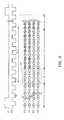
- FIG. 3shows waveforms of signals transmitted via pins TP 1 , CLK, and DD 0 -DD 3 according to the embodiment of the present invention.
- FIG. 2is a simplified block diagram of an electronic display apparatus according to an embodiment of the present invention.
- the electronic display apparatusis a TFT-LCD.
- signalsare transmitted from a signal source, which is a timing controller 210 in this embodiment, to a source driver 220 via I/O pins TP 1 , CLK and DD 0 -DD 3 .
- the I/O pin TP 1is a synchronous signal pin
- the I/O pin CLKis a clock signal pin
- each of the I/O pins DD 0 -DD 3is a data pin.
- This embodimentis exemplified by utilizing four data pins DD 0 -DD 3 , but the present invention is not limited thereto.
- FIG. 3is a timing diagram showing waveforms of signals transmitted via the pins TP 1 , CLK, and DD 0 -DD 3 according to the embodiment of the present invention.
- a plurality of setting signalswhich are used to adjust the setting of the electronic display apparatus, are transmitted to the source driver 220 via the pins DD 0 -DD 3 .
- the timing controller 210After outputting a transfer pulse of a synchronous signal TP 1 , the timing controller 210 sends signals, for driving pixels of the panel 230 , to the source driver 220 .
- signals transmitted via the pins DD 0 -DD 3are kept to be 0 (i.e. low) due to the preservation of energy.
- each of the pins DD 0 -DD 3transmits a start pulse pattern STH, e.g. a data sequence of “1-1-0-1” in this embodiment, to the source driver 220 .
- the start pulse pattern STHnotices the source driver 220 to receive the setting signals and the display data signals for driving the pixels of the panel 230 .
- the timing controller 210After outputting the start pulse pattern STH, the timing controller 210 transmits the setting signals to the source driver 220 via the data pins DD 0 -DD 3 within a setting period T 3 such that the electronic display apparatus could be set according to the setting signals. It should be noted that it is not necessary to use all of the data pins DD 0 -DD 3 to transmit the start pulse pattern STH. For example, in other embodiments of the present invention, only one or part of the data pins DD 0 -DD 3 is used for the transmission of the start pulse pattern STH.
- the setting signalsare sent from the timing controller 210 to the source driver 220 via one or more data pins in the embodiment, the setting signals are transmitted to the source driver 220 via the pins DD 0 -DD 1 during the setting period T 3 .
- Every clock of the clock signal CLK within the setting period T 3two of the setting signals are transmitted to the source driver 220 by each one of the pins DD 0 -DD 1 .
- the setting signals transmitted via DD 0 -DD 1 during the setting period T 3may include, for example, DIR, POL, LP, RS, FME, MODE 1 /MODE 2 , VA 0 , VA 1 , VB 0 , and VB 1 , which will be explained later.
- the transmission sequence of the setting signalsmay be different in other embodiments of the present invention, and the quantity of the setting signals may be changed based on specific design of the source driver and the timing controller. Since two of the setting signals are outputted to the source driver 220 by each one of the pins DD 0 -DD 1 within every clock of the clock signal CLK, the required I/O pins for transmitting the setting signals could be reduced as compared with the prior art.
- the setting signal DIRis a shift direction control signal that indicates the shift direction of shift registers positioned in the source driver 220 .
- the setting signal DIR with logic highindicates the shift direction is from left channel to the right channel.
- the setting signal DIR with logic lowindicates the shift direction is from right channel to left channel.
- the setting signal POLis a polarity inverting control signal that indicates polarity for the panel 230 of the electronic display apparatus.
- the setting signal POLis high, gamma reference voltages V ⁇ 11 to V ⁇ 20 are related to output buffers OUT 2n-1 (n is a positive integer), and gamma reference voltages V ⁇ 1 to V ⁇ 10 are related to output buffers OUT 2n .
- the setting signal POLis low, the gamma reference voltages V ⁇ 1 to V ⁇ 10 are related to output buffers OUT 2n-1 , and the gamma reference voltages V ⁇ 11 to V ⁇ 20 are related to output buffers OUT 2n .
- the setting signal LPis a low power mode signal that indicates power consumption mode of the source driver 220 .
- the setting signal LPis low, the source driver 220 operates in a low power mode.
- the setting signal LPis high, the source driver 220 operates in a normal power mode.
- the setting signal RSis a driving setting signal which indicates the driving ability of the source driver.
- the source driver 220operates with heavy load.
- the setting signal RSis high, the source driver 220 operates with light load.
- the setting signal FMEis a frame signal input signal which indicates a gate driver start pulse for the electronic display apparatus.
- one of the signals transmitted by the pin DD 0is “MODE 1 ”, and one of the signals transmitted by the pin DD 1 is “MODE 2 ”.
- Either the setting signal MODE 1 or the setting signal MODE 2is a pixel arrangement mode control signal which indicates a pixel arrangement mode for the panel 230 .
- one of the signals transmitted by the pin DD 0 or DD 1is “VA 0 ” or “VA 1 ”.
- Both the setting signals “VA 0 ” and “VA 1 ”are slew rate enhancement signals which indicate the slew rate of corresponding operational amplifiers of the source driver 220 .
- the default value of the setting signal VA 1is low, and the default value of the setting signal VA 0 is high.
- the bias current of the operational amplifiersis equal to 100% of a maximum bias current such that the panel 230 operates with the most energy-consumed power.
- VA 1is low and VA 0 is high, the bias current of the operational amplifiers is equal to 80% of the maximum bias current.
- the bias current of the operational amplifiersis 67% of the maximum bias current. Further, when VA 1 is high and VA 0 is low, the bias current of the maximum bias current is 57% of the maximum bias current such that the panel 230 operates with the least energy-consumed power.
- both the setting signals VB 0 and VB 1are RSDS (reduced swing differential signaling) bias enhancement signals which indicates the RSDS bias control for the source driver 220 .
- the default value of the setting signal VB 1is low, and the default value of the setting signal VB 0 is high.
- the RSDS bias currentis equal to a maximum RSDS bias.
- the RSDS bias currentis equal to 80% of the maximum RSDS bias.
- the RSDS bias currentis equal to 67% of the maximum RSDS bias.
- the RSDS bias currentis equal to 57% of the maximum RSDS bias.
- the sub-period with symbols “Res” of the pins DD 0 and DD 1could be reserved to send other setting signals if necessary, Similarly, the sub-periods with marks “0” of the pins DD 2 -DD 3 within the setting period T 3 could be used to send other setting signals if necessary.
- display data signals D 26 -D 29for determining display values of the pixels of the panel 230 , are transmitted by the pins DD 0 -DD 3 . Then, when another transfer pulse of the synchronous signal TP 1 is received, the source driver 220 drives the panel 230 according to the display data signals received within the period of T 4 .
- a method for driving the electronic display apparatusincludes: (a) transmitting the synchronous signal TP 1 from the timing controller 210 to the source driver 220 via the synchronous signal pin during the period T 1 ; (b) transmitting the clock signal CLK from the timing controller 210 to the source driver 220 via the clock signal pin; (c) keeping the data pins with logic low during the period T 1 (optional for power saving); (d) sending the start pulse pattern STH, and then sending setting signals, from the timing controller 210 to the source driver 220 via the data pins DD 0 -DD 3 during the period T 2 ; (e) during the setting period T 3 , sending the display data signals from the timing controller 210 to the source driver 220 via the data pins DD 0 -DD 3 ; and (f) decoding the received setting signals and the received display data signals to drive the panel 230 .
Landscapes
- Engineering & Computer Science (AREA)
- Chemical & Material Sciences (AREA)
- Crystallography & Structural Chemistry (AREA)
- Physics & Mathematics (AREA)
- Computer Hardware Design (AREA)
- General Physics & Mathematics (AREA)
- Theoretical Computer Science (AREA)
- Control Of Indicators Other Than Cathode Ray Tubes (AREA)
Abstract
Description
Claims (12)
Priority Applications (3)
| Application Number | Priority Date | Filing Date | Title |
|---|---|---|---|
| US12/129,254US8421779B2 (en) | 2008-05-29 | 2008-05-29 | Display and method thereof for signal transmission |
| TW97129548ATWI467533B (en) | 2008-05-29 | 2008-08-04 | Display and methods thereof for signal transmission and driving |
| CNA2008102142444ACN101593481A (en) | 2008-05-29 | 2008-08-29 | Display, signal transmission method thereof and driving method of source driver |
Applications Claiming Priority (1)
| Application Number | Priority Date | Filing Date | Title |
|---|---|---|---|
| US12/129,254US8421779B2 (en) | 2008-05-29 | 2008-05-29 | Display and method thereof for signal transmission |
Publications (2)
| Publication Number | Publication Date |
|---|---|
| US20090295762A1 US20090295762A1 (en) | 2009-12-03 |
| US8421779B2true US8421779B2 (en) | 2013-04-16 |
Family
ID=41379201
Family Applications (1)
| Application Number | Title | Priority Date | Filing Date |
|---|---|---|---|
| US12/129,254Expired - Fee RelatedUS8421779B2 (en) | 2008-05-29 | 2008-05-29 | Display and method thereof for signal transmission |
Country Status (3)
| Country | Link |
|---|---|
| US (1) | US8421779B2 (en) |
| CN (1) | CN101593481A (en) |
| TW (1) | TWI467533B (en) |
Families Citing this family (19)
| Publication number | Priority date | Publication date | Assignee | Title |
|---|---|---|---|---|
| US8421779B2 (en)* | 2008-05-29 | 2013-04-16 | Himax Technologies Limited | Display and method thereof for signal transmission |
| EP2315098A3 (en)* | 2009-10-20 | 2014-07-02 | BlackBerry Limited | Enhanced fast reset in mobile wireless communication devices and associated methods |
| KR101187571B1 (en) | 2010-12-28 | 2012-10-05 | 주식회사 실리콘웍스 | Method of data transmission of Timing Controller and Source Driver added Bit Error Rate Tester and Device thereof |
| TW201516997A (en)* | 2013-10-29 | 2015-05-01 | Novatek Microelectronics Corp | Source driver and driving method thereof |
| CN104616613B (en)* | 2013-11-04 | 2018-05-18 | 联咏科技股份有限公司 | Source electrode driver and its driving method |
| TWI521491B (en)* | 2014-04-07 | 2016-02-11 | 友達光電股份有限公司 | Data transmission system and operating method of display |
| CN105390106B (en)* | 2015-12-07 | 2018-12-21 | 深圳市华星光电技术有限公司 | The level shifting circuit and level conversion method of liquid crystal display panel of thin film transistor |
| WO2017129517A1 (en) | 2016-01-27 | 2017-08-03 | Philips Lighting Holding B.V. | Peripheral device, system including the peripheral device and method |
| CN105810169A (en)* | 2016-05-25 | 2016-07-27 | 深圳市华星光电技术有限公司 | Drive system and method of liquid crystal display |
| CN105976778B (en) | 2016-07-04 | 2019-01-11 | 深圳市华星光电技术有限公司 | The data-driven system of liquid crystal display panel |
| TWI646515B (en)* | 2018-01-19 | 2019-01-01 | 友達光電股份有限公司 | Display device |
| TWI692720B (en)* | 2018-06-21 | 2020-05-01 | 和碩聯合科技股份有限公司 | Method for setting display panel dynamically and electronic device |
| CN108806598B (en)* | 2018-08-31 | 2020-04-03 | 京东方科技集团股份有限公司 | Display device and driver and method thereof |
| TWI687914B (en)* | 2018-09-26 | 2020-03-11 | 大陸商北京集創北方科技股份有限公司 | Pulse signal control module, synchronous pulse signal generation method, source driver and display device |
| CN109166543B (en)* | 2018-09-26 | 2023-10-24 | 北京集创北方科技股份有限公司 | Data synchronization method, driving device and display device |
| CN110060632A (en)* | 2019-05-10 | 2019-07-26 | 深圳市华星光电技术有限公司 | Display drive system and display drive method |
| CN111986628A (en)* | 2019-05-22 | 2020-11-24 | 奇景光电股份有限公司 | Display control system and time schedule controller thereof |
| TWI750979B (en)* | 2020-12-30 | 2021-12-21 | 新唐科技股份有限公司 | Control device and display device for reducing usage pin of component |
| US12248353B1 (en)* | 2023-09-07 | 2025-03-11 | Himax Technologies Limited | Method of performing power saving control on display device and related display device |
Citations (11)
| Publication number | Priority date | Publication date | Assignee | Title |
|---|---|---|---|---|
| US20050168428A1 (en)* | 2000-12-06 | 2005-08-04 | Sony Corporation | Timing generation circuit for display apparatus and display apparatus incorporating the same |
| US20050264546A1 (en)* | 2004-05-27 | 2005-12-01 | Chun-Yi Chou | Source driver, source driver array, and driver with the source driver array and display with the driver |
| US20060262065A1 (en)* | 2005-05-23 | 2006-11-23 | Sunplus Technology Co., Ltd. | Control circuit and control method for LCD panel |
| TW200705373A (en) | 2005-07-22 | 2007-02-01 | Himax Tech Inc | TFT LCD source driver |
| TWI277793B (en) | 2005-05-10 | 2007-04-01 | Novatek Microelectronics Corp | Source driving device and timing control method thereof |
| TWI285998B (en) | 2002-06-27 | 2007-08-21 | Samsung Electronics Co Ltd | Data transmission circuit and method for reducing leakage current |
| US7259739B2 (en)* | 2002-04-20 | 2007-08-21 | Lg.Philips Lcd Co., Ltd. | Method and apparatus for driving liquid crystal display |
| US20080143665A1 (en)* | 2006-12-19 | 2008-06-19 | Nec Electronics Corporation | Display apparatus, source driver, and display panel driving method |
| US20090128475A1 (en)* | 2006-09-05 | 2009-05-21 | Himax Technologies Limited | Method for transmitting control signals and pixel data signals to source drives of an LCD |
| US20090295762A1 (en)* | 2008-05-29 | 2009-12-03 | Himax Technologies Limited | Display and method thereof for signal transmission |
| US7705841B2 (en)* | 2006-01-20 | 2010-04-27 | Novatek Microelectronics Corp. | Display system and method for embeddedly transmitting data signals, control signals, clock signals and setting signals |
- 2008
- 2008-05-29USUS12/129,254patent/US8421779B2/ennot_activeExpired - Fee Related
- 2008-08-04TWTW97129548Apatent/TWI467533B/ennot_activeIP Right Cessation
- 2008-08-29CNCNA2008102142444Apatent/CN101593481A/enactivePending
Patent Citations (12)
| Publication number | Priority date | Publication date | Assignee | Title |
|---|---|---|---|---|
| US20050168428A1 (en)* | 2000-12-06 | 2005-08-04 | Sony Corporation | Timing generation circuit for display apparatus and display apparatus incorporating the same |
| US7259739B2 (en)* | 2002-04-20 | 2007-08-21 | Lg.Philips Lcd Co., Ltd. | Method and apparatus for driving liquid crystal display |
| TWI285998B (en) | 2002-06-27 | 2007-08-21 | Samsung Electronics Co Ltd | Data transmission circuit and method for reducing leakage current |
| US20050264546A1 (en)* | 2004-05-27 | 2005-12-01 | Chun-Yi Chou | Source driver, source driver array, and driver with the source driver array and display with the driver |
| TWI277793B (en) | 2005-05-10 | 2007-04-01 | Novatek Microelectronics Corp | Source driving device and timing control method thereof |
| US20060262065A1 (en)* | 2005-05-23 | 2006-11-23 | Sunplus Technology Co., Ltd. | Control circuit and control method for LCD panel |
| TW200641749A (en) | 2005-05-23 | 2006-12-01 | Sunplus Technology Co Ltd | Control circuit and method for liquid crystal display |
| TW200705373A (en) | 2005-07-22 | 2007-02-01 | Himax Tech Inc | TFT LCD source driver |
| US7705841B2 (en)* | 2006-01-20 | 2010-04-27 | Novatek Microelectronics Corp. | Display system and method for embeddedly transmitting data signals, control signals, clock signals and setting signals |
| US20090128475A1 (en)* | 2006-09-05 | 2009-05-21 | Himax Technologies Limited | Method for transmitting control signals and pixel data signals to source drives of an LCD |
| US20080143665A1 (en)* | 2006-12-19 | 2008-06-19 | Nec Electronics Corporation | Display apparatus, source driver, and display panel driving method |
| US20090295762A1 (en)* | 2008-05-29 | 2009-12-03 | Himax Technologies Limited | Display and method thereof for signal transmission |
Non-Patent Citations (1)
| Title |
|---|
| "Office Action of Taiwan counterpart application" issued on Oct. 24, 2012, p1-p12, in which the listed references were cited. |
Also Published As
| Publication number | Publication date |
|---|---|
| TWI467533B (en) | 2015-01-01 |
| TW200949790A (en) | 2009-12-01 |
| CN101593481A (en) | 2009-12-02 |
| US20090295762A1 (en) | 2009-12-03 |
Similar Documents
| Publication | Publication Date | Title |
|---|---|---|
| US8421779B2 (en) | Display and method thereof for signal transmission | |
| KR101286541B1 (en) | Liquid crystal display | |
| US7518600B2 (en) | Connector and apparatus of driving liquid crystal display using the same | |
| US9240154B2 (en) | Liquid crystal display | |
| US8009130B2 (en) | Liquid crystal display device and method of driving the same | |
| US9001017B2 (en) | Liquid crystal display device using a mini-LVDS method | |
| US20140118235A1 (en) | Display device and method for driving the same | |
| KR20150125145A (en) | Display Device | |
| US7973785B2 (en) | Control board and display apparatus having the same | |
| KR101696458B1 (en) | Liquid crystal display | |
| US9711076B2 (en) | Display device | |
| KR20090085424A (en) | Display device and driving method | |
| KR20160078614A (en) | Display device | |
| KR20070056779A (en) | Data driving integrated circuit device and liquid crystal display device including the same | |
| KR20150073642A (en) | Timing controller and display apparatus having the same | |
| KR20030061552A (en) | Apparatus and method for transfering data | |
| KR20120068414A (en) | Liquid crystal display | |
| KR101761417B1 (en) | Liquid crystal display | |
| KR20110043889A (en) | LCD and its driving method | |
| KR102494149B1 (en) | Data driving circuit and image display device | |
| KR20190080292A (en) | Electronic device including display apparatus and method for driving the same | |
| KR101629515B1 (en) | Liquid crystal display | |
| KR101502370B1 (en) | Liquid crystal display | |
| KR20160089975A (en) | Source driver and display device having the same | |
| JP2003223148A (en) | Method for driving liquid crystal display device and liquid crystal display device |
Legal Events
| Date | Code | Title | Description |
|---|---|---|---|
| AS | Assignment | Owner name:HIMAX TECHNOLOGIES LIMITED,TAIWAN Free format text:ASSIGNMENT OF ASSIGNORS INTEREST;ASSIGNORS:FAN, WEN-TENG;CHEN, CHIEN-RU;REEL/FRAME:021026/0582 Effective date:20080201 Owner name:HIMAX TECHNOLOGIES LIMITED, TAIWAN Free format text:ASSIGNMENT OF ASSIGNORS INTEREST;ASSIGNORS:FAN, WEN-TENG;CHEN, CHIEN-RU;REEL/FRAME:021026/0582 Effective date:20080201 | |
| STCF | Information on status: patent grant | Free format text:PATENTED CASE | |
| FPAY | Fee payment | Year of fee payment:4 | |
| FEPP | Fee payment procedure | Free format text:MAINTENANCE FEE REMINDER MAILED (ORIGINAL EVENT CODE: REM.); ENTITY STATUS OF PATENT OWNER: LARGE ENTITY | |
| LAPS | Lapse for failure to pay maintenance fees | Free format text:PATENT EXPIRED FOR FAILURE TO PAY MAINTENANCE FEES (ORIGINAL EVENT CODE: EXP.); ENTITY STATUS OF PATENT OWNER: LARGE ENTITY | |
| STCH | Information on status: patent discontinuation | Free format text:PATENT EXPIRED DUE TO NONPAYMENT OF MAINTENANCE FEES UNDER 37 CFR 1.362 | |
| FP | Lapsed due to failure to pay maintenance fee | Effective date:20210416 |