US8419457B2 - Anti-electromagnetic interference electrical connector and terminal assembly thereof - Google Patents
Anti-electromagnetic interference electrical connector and terminal assembly thereofDownload PDFInfo
- Publication number
- US8419457B2 US8419457B2US13/218,721US201113218721AUS8419457B2US 8419457 B2US8419457 B2US 8419457B2US 201113218721 AUS201113218721 AUS 201113218721AUS 8419457 B2US8419457 B2US 8419457B2
- Authority
- US
- United States
- Prior art keywords
- terminals
- terminal
- fixing seat
- terminal assembly
- sectional area
- Prior art date
- Legal status (The legal status is an assumption and is not a legal conclusion. Google has not performed a legal analysis and makes no representation as to the accuracy of the status listed.)
- Active
Links
Images


Classifications
- H—ELECTRICITY
- H01—ELECTRIC ELEMENTS
- H01R—ELECTRICALLY-CONDUCTIVE CONNECTIONS; STRUCTURAL ASSOCIATIONS OF A PLURALITY OF MUTUALLY-INSULATED ELECTRICAL CONNECTING ELEMENTS; COUPLING DEVICES; CURRENT COLLECTORS
- H01R13/00—Details of coupling devices of the kinds covered by groups H01R12/70 or H01R24/00 - H01R33/00
- H01R13/646—Details of coupling devices of the kinds covered by groups H01R12/70 or H01R24/00 - H01R33/00 specially adapted for high-frequency, e.g. structures providing an impedance match or phase match
- H01R13/6461—Means for preventing cross-talk
- H01R13/6471—Means for preventing cross-talk by special arrangement of ground and signal conductors, e.g. GSGS [Ground-Signal-Ground-Signal]
- H—ELECTRICITY
- H01—ELECTRIC ELEMENTS
- H01R—ELECTRICALLY-CONDUCTIVE CONNECTIONS; STRUCTURAL ASSOCIATIONS OF A PLURALITY OF MUTUALLY-INSULATED ELECTRICAL CONNECTING ELEMENTS; COUPLING DEVICES; CURRENT COLLECTORS
- H01R12/00—Structural associations of a plurality of mutually-insulated electrical connecting elements, specially adapted for printed circuits, e.g. printed circuit boards [PCB], flat or ribbon cables, or like generally planar structures, e.g. terminal strips, terminal blocks; Coupling devices specially adapted for printed circuits, flat or ribbon cables, or like generally planar structures; Terminals specially adapted for contact with, or insertion into, printed circuits, flat or ribbon cables, or like generally planar structures
- H01R12/70—Coupling devices
- H01R12/71—Coupling devices for rigid printing circuits or like structures
- H01R12/72—Coupling devices for rigid printing circuits or like structures coupling with the edge of the rigid printed circuits or like structures
- H01R12/721—Coupling devices for rigid printing circuits or like structures coupling with the edge of the rigid printed circuits or like structures cooperating directly with the edge of the rigid printed circuits
Definitions
- This disclosurerelates to an electrical connector, and more particularly to an anti-electromagnet interference (EMI) electrical connector and a terminal assembly thereof.
- EMIanti-electromagnet interference
- a signal terminalperforms signal transmission through high-frequency current switching. Therefore, when a high-frequency current passes through the signal terminal and is switched rapidly, a magnetic field is generated around the signal terminal.
- a pitch between the terminalsis quite small, since the number of small-sized signal terminals is high.
- an EMI phenomenonis likely to occur between the adjacent signal terminals, causing a transmission error, and affecting a transmission efficiency of the signal terminals.
- a terminal arrangement manner thereofis to arrange the signal terminals and ground pins in a staggered manner with intervals, so as to shield the EMI between the adjacent signal terminals through the ground pins.
- DDRDouble Data Rate
- the above ground pincan only shield the EMI to a limited degree; if the arrangement of the terminals is more intensive, a shielding effect of the ground pin is very limited.
- this disclosureprovides an anti-electromagnet interference (EMI) electrical connector and a terminal assembly thereof, so as to eliminate EMI between terminals.
- EMIanti-electromagnet interference
- At least one embodiment of this disclosureprovides an anti-electromagnet interference (EMI) electrical connector.
- the anti-EMI electrical connectorincludes an electrical insulation case, a plurality of first terminals, and a plurality of second terminals.
- the electrical insulation caseincludes a slot.
- Each of the first terminalsis respectively disposed in the electrical insulation case, and each of the first terminals respectively includes a contact end located in the slot.
- Each of the second terminalsis respectively disposed in the electrical insulation case, and the second terminals and the first terminals are arranged in a staggered manner.
- Each of the second terminalsrespectively includes a connection end located in the slot and adjacent to the contact end of at least one first terminal, in which a sectional area of the connection end of the second terminal is larger than a sectional area of the contact end of the first terminal.
- connection endis larger than the sectional area of the contact end. Therefore, when a high-frequency signal is transmitted between the first terminals, the resulting the resulting EMI is effectively blocked by the connection end of the second terminal, thereby eliminating the EMI between the first terminals.
- At least one embodiment of this disclosurefurther provides a terminal assembly.
- the terminal assemblyis provided to be combined with an electrical insulation case, so as to form an anti-EMI electrical connector.
- the terminal assemblyincludes a fixing seat, a plurality of first terminals, and a plurality of second terminals.
- the first terminalsare fixed on the fixing seat, and each of the first terminals respectively includes a contact end.
- the second terminalsare fixed on the fixing seat, in which the second terminals and the first terminals are arranged in a staggered manner.
- Each of the second terminalsrespectively includes a connection end adjacent to the contact end of at least one first terminal, and a sectional area of the connection end is larger than a sectional area of the contact end.
- the sectional area of the connection endis larger than the sectional area of the contact end. Therefore, when a high-frequency signal is transmitted by the first terminals, the resulting EMI is effectively shielded by the connection end of the second terminals, thereby eliminating the EMI between the first terminals.
- the sectional area of the connection endis larger than the sectional area of the contact end, that is, the sectional area of the second terminal is increased to increase an effective shielding area and improve electrical characteristics.
- shielding of the second terminalcan be used to block the EMI, therefore achieving an objective of maintaining electronic signal quality.
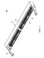
- FIG. 1is a perspective view of a first embodiment
- FIG. 2is an exploded view of a first embodiment
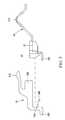
- FIG. 3is a perspective view of a terminal according to a first embodiment
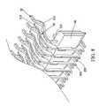
- FIG. 4is an exploded view of a second embodiment
- FIG. 5is a side view of a terminal assembly according to a second embodiment
- FIG. 6is another side view of a terminal assembly according to a second embodiment
- FIG. 7is an enlarged perspective view of a terminal assembly according to a second embodiment
- FIG. 8is another enlarged perspective view of a terminal assembly according to a second embodiment.
- FIG. 9is another enlarged perspective view of a second embodiment.
- an anti-EMI electrical connectoraccording to a first embodiment is provided to be electrically connected to an electrical plug (not shown).
- the anti-EMI electrical connectorincludes an electrical insulation case 10 , a plurality of first terminals 20 , and a plurality of second terminals 30 .
- the electrical insulation case 10includes a slot 110 .
- the above-mentioned the electrical plugis provided to be inserted into the slot 110 correspondingly.
- the slot 110is in a slim shape, and the electrical plug has a flat shape matching the slot 110 , and is located at an edge of the DDR memory module.
- the first terminals 20are disposed in the electrical insulation case 10 , and each of the first terminals 20 respectively includes a contact end 210 .
- the contact ends 210are located in the slot 110 of the electrical insulation case 10 .
- the first terminals 20are used for signal transmission, and in detail, each of the first terminals is a signal transmission terminal.
- the first terminal 20further includes a first welding end 220 and a first locating end 230 .
- the first welding end 220is provided to be welded on a circuit board, such as a computer motherboard, so that the electrical connector is fixed on the circuit board through the first welding end 220 of the first terminal 20 , and further electrically connects the circuit board.
- the first locating end 230is provided to be combined with the electrical insulation case 10 , in which the first locating end 230 further includes a barb 231 for snapping the electrical insulation case 10 , therefore the first terminal is combined with the electrical insulation case 10 in a clamping manner.
- the second terminals 30are disposed in the electrical insulation case 10 .
- the second terminals 30 and the first terminals 20are arranged in a staggered manner, that is, one first terminal 20 is followed by one second terminal 30 .
- Each of the second terminals 30includes a connection end 310 located in the slot 110 and adjacent to at least one of the contact ends 210 of the first terminals 20 .
- the connection end 310 at an outermost sideis located at a side edge of one contact end 210 , but the connection end 310 and the contact end 210 do not contact each other; and the rest of the connection ends 310 are located between the two contact ends 210 .
- the number of the connection ends 310 and the contact ends 210may be set correspondingly, or the number of the connection ends 310 may be larger than, equal to, or smaller than the number of the contact ends 210 .
- a sectional area of the connection end 310 of the second terminal 30is larger than a sectional area of the contact end 210 of the first terminal 20 .
- the sectional area of the contact end 210 of the second terminal 30is increased to increase an effective shielding area of the contact end 210 and improve electrical characteristics. Therefore, when the first terminal 20 performs data transmission, shielding of the second terminal 30 can be used to restrain EMI of each of the first terminals 20 , so as to maintain quality of an electronic signal.
- the second terminals 30are electrically grounded to serve as ground pins. It is noted that, in order to increase the sectional area of the second terminal 30 , an original insert molding structure is modified to an insert terminal structure.
- Each of the second terminals 30further includes a second welding end 320 and a second locating end 330 .
- the second welding end 320is provided to be welded on a circuit board, such as a computer motherboard, so that the electrical connector is fixed on the circuit board through the second welding end 320 of the second terminal 20 , and further electrically connects a grounding circuit of the circuit board.
- the second locating end 330is provided to be combined with the electrical insulation case 10 .
- the second locating end 330further includes a barb 331 for snapping the electrical insulation case 10 .
- the electrical connector 100further includes a positioning member 80 disposed in the electrical insulation case 10 for positioning and latching the electrical plug.
- a positioning member 80disposed in the electrical insulation case 10 for positioning and latching the electrical plug.
- a terminal assembly 200according a second embodiment is provided to be combined with the electrical insulation case 10 , so as to form an anti-EMI electrical connector.
- the terminal assembly 200includes a fixing seat 40 , a plurality of first terminals 20 , and a plurality of second terminals 30 .
- the first terminals 20are fixed on the fixing seat 40 , and each of the first terminals 20 respectively includes a contact end 210 .
- the second terminals 30are fixed on the fixing seat 40 .
- the second terminals 30 and the first terminals 20are arranged in a staggered manner.
- Each of the second terminals 30respectively includes a connection end 310 adjacent to at least one contact end 210 , and a sectional area of the connection end 310 is larger than a sectional area of the contact end 210 .
- fixing slots 41is formed on the fixing seat 40 , and each of the second terminals 30 respectively includes a second locating end 330 and a third locating end 340 . At least one of the second locating end 330 and the third locating end 340 is embedded into the fixing slot 41 , so that second locating end 330 and the third locating end 340 clamps the fixing seat 40 , thereby combining the second terminal 30 with the fixing seat 40 .
- the third locating end 340further includes a barb 341 for snapping the fixing seat 40 ; therefore the second terminal 30 is combined with the fixing seat 40 in an inserting manner.
- This description of the second terminal 30 combined with the fixing seat 40is merely an example, and substitute methods may be used to combine the second terminals 30 with the fixing seat 40 through inserting, or combine the first terminals 20 or the second terminals 30 with the fixing seat 40 in an insert molding manner.
- the sectional area of the contact end 210 of the second terminal 30is increased to increase an effective shielding area of the contact end 210 and improve electrical characteristics. Therefore, when the first terminal 20 performs data transmission, shielding of the second terminal 30 can be used to block EMI of each of the first terminals 20 , so as to maintain quality of an electronic signal. Therefore, in the second embodiment, after the terminal assembly 200 is combined with the electrical insulation case 10 , the first terminal 20 and the second terminal 30 are corresponding to the slot 110 , which forms an anti-EMI electrical connector.
Landscapes
- Details Of Connecting Devices For Male And Female Coupling (AREA)
Abstract
Description
Claims (6)
Priority Applications (1)
| Application Number | Priority Date | Filing Date | Title |
|---|---|---|---|
| US13/218,721US8419457B2 (en) | 2011-08-26 | 2011-08-26 | Anti-electromagnetic interference electrical connector and terminal assembly thereof |
Applications Claiming Priority (1)
| Application Number | Priority Date | Filing Date | Title |
|---|---|---|---|
| US13/218,721US8419457B2 (en) | 2011-08-26 | 2011-08-26 | Anti-electromagnetic interference electrical connector and terminal assembly thereof |
Publications (2)
| Publication Number | Publication Date |
|---|---|
| US20130052865A1 US20130052865A1 (en) | 2013-02-28 |
| US8419457B2true US8419457B2 (en) | 2013-04-16 |
Family
ID=47744345
Family Applications (1)
| Application Number | Title | Priority Date | Filing Date |
|---|---|---|---|
| US13/218,721ActiveUS8419457B2 (en) | 2011-08-26 | 2011-08-26 | Anti-electromagnetic interference electrical connector and terminal assembly thereof |
Country Status (1)
| Country | Link |
|---|---|
| US (1) | US8419457B2 (en) |
Cited By (3)
| Publication number | Priority date | Publication date | Assignee | Title |
|---|---|---|---|---|
| US20120270445A1 (en)* | 2011-04-20 | 2012-10-25 | Hosiden Corporation | Connector |
| US20140090246A1 (en)* | 2007-12-20 | 2014-04-03 | Trw Automotive U.S. Llc | Electronic assembly and method of manufacturing same |
| US10128620B1 (en)* | 2017-09-27 | 2018-11-13 | Greenconn Corp. | High speed vertical connector |
Families Citing this family (2)
| Publication number | Priority date | Publication date | Assignee | Title |
|---|---|---|---|---|
| US10103476B1 (en)* | 2017-08-10 | 2018-10-16 | Amphenol East Asia Electronic Technology (Shen Zhen) Co., Ltd. | DDR socket connector |
| CN112202503B (en)* | 2020-09-22 | 2022-08-26 | 展讯通信(上海)有限公司 | Interference processing method, terminal equipment and computer readable storage medium |
Citations (26)
| Publication number | Priority date | Publication date | Assignee | Title |
|---|---|---|---|---|
| US5259768A (en)* | 1992-03-24 | 1993-11-09 | Molex Incorporated | Impedance and inductance control in electrical connectors and including reduced crosstalk |
| US5522737A (en)* | 1992-03-24 | 1996-06-04 | Molex Incorporated | Impedance and inductance control in electrical connectors and including reduced crosstalk |
| US5580257A (en)* | 1995-04-28 | 1996-12-03 | Molex Incorporated | High performance card edge connector |
| US5813883A (en)* | 1996-09-11 | 1998-09-29 | Lin; Yu Chuan | Connector for micro channel printed circuit board |
| US6015299A (en)* | 1998-07-22 | 2000-01-18 | Molex Incorporated | Card edge connector with symmetrical board contacts |
| US6095821A (en)* | 1998-07-22 | 2000-08-01 | Molex Incorporated | Card edge connector with improved reference terminals |
| US6254435B1 (en)* | 1999-06-01 | 2001-07-03 | Molex Incorporated | Edge card connector for a printed circuit board |
| US6358061B1 (en)* | 1999-11-09 | 2002-03-19 | Molex Incorporated | High-speed connector with shorting capability |
| US6361367B1 (en)* | 1998-08-20 | 2002-03-26 | Fujitsu Takamisawa Component Ltd. | Plug connector |
| US6394823B1 (en)* | 2000-05-26 | 2002-05-28 | Molex Incorporated | Connector with terminals having increased capacitance |
| US20030003804A1 (en)* | 1999-12-29 | 2003-01-02 | Berg Technology, Inc. | High speed card edge connectors |
| US20030060083A1 (en)* | 1997-05-30 | 2003-03-27 | Fujitsu Takamisawa Component Limited | High density connector for balanced transmission lines |
| US20040018759A1 (en)* | 2002-07-29 | 2004-01-29 | Jerry Wu | Electrical connector assembly |
| US20040242071A1 (en)* | 2003-05-27 | 2004-12-02 | Fujitsu Component Limited | Plug connector for differential transmission |
| US6994563B2 (en)* | 2003-12-19 | 2006-02-07 | Lenovo (Singapore) Pte. Ltd. | Signal channel configuration providing increased capacitance at a card edge connection |
| US7048567B2 (en)* | 2002-05-10 | 2006-05-23 | Molex Incorporated | Edge card connector assembly with tuned impedance terminals |
| US20070184718A1 (en)* | 2006-02-07 | 2007-08-09 | Fujitsu Component Limited | High speed transmission connector |
| US7410392B2 (en)* | 2005-12-15 | 2008-08-12 | Tyco Electronics Corporation | Electrical connector assembly having selective arrangement of signal and ground contacts |
| US7591684B2 (en)* | 2006-10-12 | 2009-09-22 | Hon Hai Precision Ind. Co., Ltd. | Electrical connector |
| US20100190385A1 (en)* | 2009-01-28 | 2010-07-29 | Fujitsu Component Limited | Connector device |
| US7806730B2 (en)* | 2005-12-15 | 2010-10-05 | Tyco Electronics Corporation | Electrical connector assembly having selective arrangement of signal and ground contacts |
| US7824224B2 (en)* | 2008-11-28 | 2010-11-02 | Nextronics Engineering Corp. | Printed board connector |
| US8036284B2 (en)* | 2000-06-14 | 2011-10-11 | Rambus Inc. | Method and apparatus for transmitting data with reduced coupling noise |
| US8152539B2 (en)* | 2004-07-26 | 2012-04-10 | Fujitsu Component Limited | Connector unit for differential transmission |
| US8231411B1 (en)* | 2011-03-01 | 2012-07-31 | Tyco Electronics Corporation | Card edge connector |
| US20120225588A1 (en)* | 2011-03-01 | 2012-09-06 | Tyco Electronics Corporation | Card edge connector |
- 2011
- 2011-08-26USUS13/218,721patent/US8419457B2/enactiveActive
Patent Citations (34)
| Publication number | Priority date | Publication date | Assignee | Title |
|---|---|---|---|---|
| US5522737A (en)* | 1992-03-24 | 1996-06-04 | Molex Incorporated | Impedance and inductance control in electrical connectors and including reduced crosstalk |
| US6019639A (en)* | 1992-03-24 | 2000-02-01 | Molex Incorporated | Impedance and inductance control in electrical connectors and including reduced crosstalk |
| US5259768A (en)* | 1992-03-24 | 1993-11-09 | Molex Incorporated | Impedance and inductance control in electrical connectors and including reduced crosstalk |
| US5580257A (en)* | 1995-04-28 | 1996-12-03 | Molex Incorporated | High performance card edge connector |
| US5730609A (en)* | 1995-04-28 | 1998-03-24 | Molex Incorporated | High performance card edge connector |
| US5813883A (en)* | 1996-09-11 | 1998-09-29 | Lin; Yu Chuan | Connector for micro channel printed circuit board |
| US20030060083A1 (en)* | 1997-05-30 | 2003-03-27 | Fujitsu Takamisawa Component Limited | High density connector for balanced transmission lines |
| US6805586B2 (en)* | 1997-05-30 | 2004-10-19 | Fujitsu Takamisawa Component Limited | High density connector for balanced transmission lines |
| US6015299A (en)* | 1998-07-22 | 2000-01-18 | Molex Incorporated | Card edge connector with symmetrical board contacts |
| US6095821A (en)* | 1998-07-22 | 2000-08-01 | Molex Incorporated | Card edge connector with improved reference terminals |
| USRE38736E1 (en)* | 1998-07-22 | 2005-05-17 | Molex Incorporated | Card edge connector with symmetrical board contacts |
| US6361367B1 (en)* | 1998-08-20 | 2002-03-26 | Fujitsu Takamisawa Component Ltd. | Plug connector |
| US6254435B1 (en)* | 1999-06-01 | 2001-07-03 | Molex Incorporated | Edge card connector for a printed circuit board |
| US6358061B1 (en)* | 1999-11-09 | 2002-03-19 | Molex Incorporated | High-speed connector with shorting capability |
| US6561850B2 (en)* | 1999-12-29 | 2003-05-13 | Berg Technology, Inc. | High speed card edge connectors |
| US20030003804A1 (en)* | 1999-12-29 | 2003-01-02 | Berg Technology, Inc. | High speed card edge connectors |
| US6394823B1 (en)* | 2000-05-26 | 2002-05-28 | Molex Incorporated | Connector with terminals having increased capacitance |
| US8036284B2 (en)* | 2000-06-14 | 2011-10-11 | Rambus Inc. | Method and apparatus for transmitting data with reduced coupling noise |
| US7048567B2 (en)* | 2002-05-10 | 2006-05-23 | Molex Incorporated | Edge card connector assembly with tuned impedance terminals |
| US20040018759A1 (en)* | 2002-07-29 | 2004-01-29 | Jerry Wu | Electrical connector assembly |
| US20040242071A1 (en)* | 2003-05-27 | 2004-12-02 | Fujitsu Component Limited | Plug connector for differential transmission |
| US6923664B2 (en)* | 2003-05-27 | 2005-08-02 | Fujitsu Component Limited | Plug connector for differential transmission |
| US6994563B2 (en)* | 2003-12-19 | 2006-02-07 | Lenovo (Singapore) Pte. Ltd. | Signal channel configuration providing increased capacitance at a card edge connection |
| US8152539B2 (en)* | 2004-07-26 | 2012-04-10 | Fujitsu Component Limited | Connector unit for differential transmission |
| US7410392B2 (en)* | 2005-12-15 | 2008-08-12 | Tyco Electronics Corporation | Electrical connector assembly having selective arrangement of signal and ground contacts |
| US7806730B2 (en)* | 2005-12-15 | 2010-10-05 | Tyco Electronics Corporation | Electrical connector assembly having selective arrangement of signal and ground contacts |
| US7604510B2 (en)* | 2006-02-07 | 2009-10-20 | Fujitsu Component Limited | High speed transmission connector |
| US20070184718A1 (en)* | 2006-02-07 | 2007-08-09 | Fujitsu Component Limited | High speed transmission connector |
| US7591684B2 (en)* | 2006-10-12 | 2009-09-22 | Hon Hai Precision Ind. Co., Ltd. | Electrical connector |
| US7824224B2 (en)* | 2008-11-28 | 2010-11-02 | Nextronics Engineering Corp. | Printed board connector |
| US20100190385A1 (en)* | 2009-01-28 | 2010-07-29 | Fujitsu Component Limited | Connector device |
| US8047875B2 (en)* | 2009-01-28 | 2011-11-01 | Fujitsu Component Limited | Connector device |
| US8231411B1 (en)* | 2011-03-01 | 2012-07-31 | Tyco Electronics Corporation | Card edge connector |
| US20120225588A1 (en)* | 2011-03-01 | 2012-09-06 | Tyco Electronics Corporation | Card edge connector |
Cited By (5)
| Publication number | Priority date | Publication date | Assignee | Title |
|---|---|---|---|---|
| US20140090246A1 (en)* | 2007-12-20 | 2014-04-03 | Trw Automotive U.S. Llc | Electronic assembly and method of manufacturing same |
| US8904633B2 (en)* | 2007-12-20 | 2014-12-09 | Trw Automotive U.S. Llc | Electronic assembly and method of manufacturing same |
| US20120270445A1 (en)* | 2011-04-20 | 2012-10-25 | Hosiden Corporation | Connector |
| US8672691B2 (en)* | 2011-04-20 | 2014-03-18 | Hosiden Corporation | Connector |
| US10128620B1 (en)* | 2017-09-27 | 2018-11-13 | Greenconn Corp. | High speed vertical connector |
Also Published As
| Publication number | Publication date |
|---|---|
| US20130052865A1 (en) | 2013-02-28 |
Similar Documents
| Publication | Publication Date | Title |
|---|---|---|
| JP7353419B2 (en) | high density receptacle | |
| CN103636069B (en) | Card edge connector | |
| US10103492B2 (en) | Electrical connector with stabilizing grounding member | |
| US9455530B2 (en) | Electrical connector with ground bus | |
| US9166320B1 (en) | Cable connector assembly | |
| US8408939B2 (en) | Electrical connector system | |
| CN102176557B (en) | High density bottom plate connector | |
| US9490586B1 (en) | Electrical connector having a ground shield | |
| US7614899B2 (en) | Electrical connector assembly | |
| US8840431B2 (en) | Electrical connector systems | |
| CN101174747A (en) | Stacked Connector Assemblies | |
| US8465327B2 (en) | High-speed memory connector | |
| US10381776B2 (en) | Connector assembly with an improved latch member having a shorter length | |
| US20130264107A1 (en) | Circuit board and wire assembly | |
| US20090233492A1 (en) | Connector and Connector Device | |
| US20120003849A1 (en) | Electrical connector connecting two board shaped device | |
| US8419457B2 (en) | Anti-electromagnetic interference electrical connector and terminal assembly thereof | |
| KR101344933B1 (en) | Connector assembly | |
| CN106229764B (en) | Electrical connector with ground shield | |
| JP2012054173A (en) | Connector device having shield effect | |
| US8545272B2 (en) | Electrical connector with separating extensions on terminals | |
| US10014634B2 (en) | High speed network module socket connector | |
| US20220302653A1 (en) | Connector | |
| KR200473302Y1 (en) | Connector | |
| US20130164983A1 (en) | Connector and electronic device having same |
Legal Events
| Date | Code | Title | Description |
|---|---|---|---|
| AS | Assignment | Owner name:CONCRAFT HOLDING CO., LTD., CAYMAN ISLANDS Free format text:ASSIGNMENT OF ASSIGNORS INTEREST;ASSIGNORS:LEE, KUO-CHI;LIN, CHIN-HUANG;REEL/FRAME:026814/0016 Effective date:20110826 | |
| STCF | Information on status: patent grant | Free format text:PATENTED CASE | |
| FPAY | Fee payment | Year of fee payment:4 | |
| MAFP | Maintenance fee payment | Free format text:PAYMENT OF MAINTENANCE FEE, 8TH YEAR, LARGE ENTITY (ORIGINAL EVENT CODE: M1552); ENTITY STATUS OF PATENT OWNER: LARGE ENTITY Year of fee payment:8 | |
| AS | Assignment | Owner name:DRAGONSTATE TECHNOLOGY CO., LTD., TAIWAN Free format text:ASSIGNMENT OF ASSIGNORS INTEREST;ASSIGNOR:CONCRAFT HOLDING CO., LTD.;REEL/FRAME:068569/0042 Effective date:20240819 | |
| FEPP | Fee payment procedure | Free format text:ENTITY STATUS SET TO SMALL (ORIGINAL EVENT CODE: SMAL); ENTITY STATUS OF PATENT OWNER: SMALL ENTITY | |
| MAFP | Maintenance fee payment | Free format text:PAYMENT OF MAINTENANCE FEE, 12TH YR, SMALL ENTITY (ORIGINAL EVENT CODE: M2553); ENTITY STATUS OF PATENT OWNER: SMALL ENTITY Year of fee payment:12 |