US8416624B2 - Erase and programming techniques to reduce the widening of state distributions in non-volatile memories - Google Patents
Erase and programming techniques to reduce the widening of state distributions in non-volatile memoriesDownload PDFInfo
- Publication number
- US8416624B2 US8416624B2US13/072,387US201113072387AUS8416624B2US 8416624 B2US8416624 B2US 8416624B2US 201113072387 AUS201113072387 AUS 201113072387AUS 8416624 B2US8416624 B2US 8416624B2
- Authority
- US
- United States
- Prior art keywords
- erase
- wordlines
- pulse
- voltage
- memory cells
- Prior art date
- Legal status (The legal status is an assumption and is not a legal conclusion. Google has not performed a legal analysis and makes no representation as to the accuracy of the status listed.)
- Active, expires
Links
Images


Classifications
- G—PHYSICS
- G11—INFORMATION STORAGE
- G11C—STATIC STORES
- G11C16/00—Erasable programmable read-only memories
- G11C16/02—Erasable programmable read-only memories electrically programmable
- G11C16/06—Auxiliary circuits, e.g. for writing into memory
- G11C16/34—Determination of programming status, e.g. threshold voltage, overprogramming or underprogramming, retention
- G—PHYSICS
- G11—INFORMATION STORAGE
- G11C—STATIC STORES
- G11C16/00—Erasable programmable read-only memories
- G11C16/02—Erasable programmable read-only memories electrically programmable
- G11C16/06—Auxiliary circuits, e.g. for writing into memory
- G11C16/10—Programming or data input circuits
- G11C16/14—Circuits for erasing electrically, e.g. erase voltage switching circuits
- G11C16/16—Circuits for erasing electrically, e.g. erase voltage switching circuits for erasing blocks, e.g. arrays, words, groups
- G—PHYSICS
- G11—INFORMATION STORAGE
- G11C—STATIC STORES
- G11C16/00—Erasable programmable read-only memories
- G11C16/02—Erasable programmable read-only memories electrically programmable
- G11C16/06—Auxiliary circuits, e.g. for writing into memory
- G11C16/10—Programming or data input circuits
- G—PHYSICS
- G11—INFORMATION STORAGE
- G11C—STATIC STORES
- G11C16/00—Erasable programmable read-only memories
- G11C16/02—Erasable programmable read-only memories electrically programmable
- G11C16/06—Auxiliary circuits, e.g. for writing into memory
- G11C16/34—Determination of programming status, e.g. threshold voltage, overprogramming or underprogramming, retention
- G11C16/3404—Convergence or correction of memory cell threshold voltages; Repair or recovery of overerased or overprogrammed cells
Definitions
- This inventionrelates generally to the erasing and programming of non-volatile memories and, more specifically, to techniques for reducing the widening in state distributions that can arise from, for example, charge traps between memory cells
- non-volatile memory systemssuch as flash EEPROM devices
- the accurate storage of datais dependent upon the data being both written and read back with accuracy.
- the accurate programming of datarelies upon the individual memory cells being written into well-defined distributions of threshold voltage values for each of the data states that the memory cells may store. This is particularly true of multistate devices, with the situation becoming ever more critical as device sizes shrink and the voltage window allotted for an increasing number of states becomes smaller. Consequently there is an ongoing need to improve techniques for providing a tighter distribution of states during write operations.
- a method of operating a non-volatile memory arrayincludes one or more erase blocks, each having a plurality on memory cells formed along bitlines and wordlines.
- the methodincludes performing an erase operation on the memory cells of one or more selected erase blocks, where the erase operation includes performing a stress phase and an erase phase.
- the stress phaseincludes applying a pattern of voltage levels to the bitlines corresponding to the selected erase blocks, where the pattern includes a voltage differential between at least one pair of adjacent ones of the corresponding bit lines, and, while applying the pattern of voltage levels to the bitlines, applying a pulse of positive voltage to one or more of the wordlines corresponding to the selected erase blocks.
- the erase phaseincludes biasing the selected erase blocks to induce erasure of the memory cells of the selected erase block.
- a method of operating a non-volatile memory arrayincludes one or more erase blocks each having a plurality of memory cells formed along bitlines and wordlines and is of a NAND type of architecture where a plurality of memory cells are connected in series between first and second select gates.
- the methodincludes performing an erase operation on the memory cells of one or more selected erase blocks, where the erase operation includes a stress phase and an erase phase.
- a first high voltage pulseis applied to a first subset of one or more non-adjacent ones of the wordlines corresponding to the selected erase blocks, the first subset including at least one wordline corresponding to memory cells not adjacent to a select gate, and, while applying the high voltage pulse to the first subset of wordlines, the others of the wordlines corresponding to the selected erase blocks are set to a low voltage level.
- the erase phaseincludes biasing the selected erase blocks to induce erasure of the memory cells of the selected erase block.
- a method of writing data to a non-volatile memoryincludes performing an alternating series of program and verify phases on a selected plurality of memory cells formed along a selected wordline.
- the verify phaseincludes performing a verify operation that individually locks out from further programming selected memory cells in response to successfully verifying as programmed to a corresponding target state.
- the programming phaseincludes applying a first and a second programming pulse to the selected wordline without an intervening verify operation, wherein a non-selected wordline adjacent to the selected wordline is set to a first voltage during the first programming pulse and to a second voltage during the second voltage during the second programming pulse, wherein the first and second voltages are distinct positive voltages.
- FIG. 1shows how pre-conditioning can improve memory endurance.
- FIGS. 2Ais an exemplary composite waveform for a double-pulse pre-conditioning.
- FIGS. 2B and 2Cgive an illustration of some exemplary bias values as applied to an array when using the waveform of FIG. 2A .
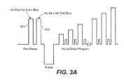
- FIG. 3Aillustrates a composite waveform that can be used in embodiments that apply a stress in the bitline direction.
- FIG. 3Bis an illustration of some exemplary bias values as applied to an array when using the waveform of FIG. 3A .
- FIG. 4shows an example of a programming waveform using double-pulse programming waveform during a write operation.
- FIGS. 5A and 5Billustrates some exemplary sequences that use pre-conditioning during an erase operation, including an optional gentle erase.
- the techniques presented belowcan be used to improve the reliability and endurance of non-volatile memories by reducing the effects of charge traps between memory cells as a non-volatile memory is cycled over many erase/program cycles.
- one way to lessen such degradation effectsis to optimize processing during manufacturing, but this is not always scalable for technology generations as devices continue to shrink in size.
- Another way to treat this problemis reducing the programming step-size to accommodate the wider distributions; however, this slows programming speeds, introducing an often unacceptable performance penalty.
- the techniques presented hereapply include a stress or conditioning phase with the erase process in order to reduce amount of charge traps between memory cells, especially for cycled cells.
- pre-stress/pre-conditioningis the application of a set of voltage stresses placed on different word lines before the erase and actual data programming (or after erase and before program). Further embodiments, presented below under the corresponding heading, use a double-pulse programming method that incorporates a stress phase into the programming operation.
- Noisefrom trapped electrons as well as other sources, can affect the accuracy of both read and write operation. Noise in the context of sensing operations, both for data reads and program verify, are considered in U.S. Pat. Nos. 6,621,739 and 6,850,441, which also discuss various aspects of memory devices in general and NAND-type devices in particular. U.S. Pat. No. 6,850,441 and references cited therein also provide some background discussion on the trapping of holes and electrons. The discussion presented here is concerned with the effect of noise on the write operation, particularly after a memory device has undergone a number of program/erase cycles. The use of pre-conditioning reduces program noise, especially for highly cycled cells, without degrading the program performance.
- FIG. 1illustrates how such pre-conditioning can improve endurance and reliability by lowering the fail bits count.
- the number of failed bits(the failed bit count, or FBC, on the vertical axis) begins to grow significantly as the number of program-erase cycles (horizontal axis) increases.
- FBCprogram-erase cycles
- non-edge wordlinesthese are also taken high in order to have little or no intra-wordline differences, specifically in order to eliminate, or at least minimize the lateral field differences between wordlines.
- the techniques presented hereenhance the pre-condition or stress operation by biasing the neighboring wordlines of wordlines selected for pre-conditioning to different voltages. (Also, although the pre-conditioning technique presented here is mainly described in the context of a NAND device, it is not so limited, whereas the “healing” technique of US patent publication US 20080298123 A1 is specifically directed at wordlines adjacent to the select gates as found at the ends of NAND strings.)
- the low values applied to a neighboring wordlinemay not taken to ground, but to a relatively low value, since having the transistors on the neighboring wordline somewhat conductive can also be useful.
- Thiscan be one of the various read or pass levels already available on the device or a specific level for this process.
- the neighboring wordlinescould be taken to something like 8V and in the even/odd arrangements discussed further down this could be on the order of 3-4V.
- Similar considerationsapply to select gates adjacent to a wordline, whether at the end of a NAND string or an adjoining select gate in other architectures; for example, in a NAND string a typical pass voltage for read operations could be used. (Again in contrast to prior art “healing” method discussed above, having the select can somewhat on, as opposed to setting its control gate at ground, can be beneficial to the process.)
- a first set of exemplary embodimentsuses a double pulse pre-conditioning/pre-stress operation, where the two consecutive pulses being applied on alternate wordlines. This can be illustrated with respect to FIGS. 2A-2C .
- FIG. 2Aschematically illustrates the double-pulse pre-stress, where one pulse is applied on even wordlines and the other on odd wordlines. (In the figures, these pulses and the other waveforms are schematic, in that the duration of the erase pulse, for example, may be relatively longer than shown.)
- the erase portion and actual data program portioncan be taken as typical operations in the prior art cited above; however, in addition to the erase phase, the erase operation now also includes the pre-stress phase.
- high voltage pulse 201is first applied to the even wordlines, while the odd wordline are biased at a lower voltage, such as ⁇ 3-4V.
- the voltage on the non-selected (here odd) wordlinecan be taken low enough so that none of the corresponding transistors are conducting, higher so that all of transistors are somewhat conducting regardless of their data state, or at an intermediate value.
- the roles of the even and odd wordlinesare then reversed for the second pulse 203 , after which the block is erased. (Here the erase phase is shown as a single pulse, although any of the standard erase operations can be used.) Once the block is erased, the various wordlines can be programmed with data.
- FIG. 2Billustrates the levels as applied for a block of a NAND array during the stress phase.
- Each of the NAND strings along the bitlines, such as 209has a plurality of memory cells connected in series between a pair of select transistors, such as 205 and 207 .
- the wordlines of the stringsare alternately even and odd, respectively labeled 0 (as for 211 ) and E (as for 213 ).
- a high voltage pulseis then applied to one set of the wordlines while the other set is set to the lower voltage, such as 3-4V.
- the rolesare then reversed for the second stress pulse.
- the select transistors at either end of the NAND stringscan be biased at a low voltage, such as ⁇ 2-3V.
- all of the bitlinesare biased at 0V.
- the embodiment of FIG. 2Csets the bitlines above ground, here at the program inhibit voltages, typically the on-chip supply level VDD.
- the even/odd arrangementapplies this voltage difference to all of the wordline lines with just a pair of pulses during the pre-stress phase.
- This schemecan enhance the pre-conditioning field and significantly reduce the fail bits count.
- other wordline stress patternscan be used. Whether for a single pulse on a single wordline, the odd/even arrangement just described, or wordline stripe pattern, pre-conditioning data shows that the greater the voltage difference between neighboring wordlines magnifies the conditioning effect, although higher field levels place more stress on the device. Consequently, the specific values will be a design choice and devices of differing design, as well as devices of the same design due to process variations, may be optimized differently.
- pulse duration, pulse voltage, neighboring wordline biascan be parameter controlled and set by the manufacturer, for example at test time. They may also be varied to account device aging or error rate as controlled by the controller or a state machine on the memory chip.
- FIG. 3Aschematically illustrates a double-pulse pre-stress, similarly to FIG. 2A , but with the first pulse on all wordlines while odd bitlines at 0V and the even bitlines inhibited at a higher voltage (here VDD), and the second pulse again on all wordlines while the even bitlines at 0V and the odd bitlines inhibited (at the higher voltage, here VDD, although other values may be used).
- VDDhigher voltage
- FIG. 3Acorrespondingly illustrates the array for this embodiment analogously to FIG. 2B for the previous odd/even wordline embodiment.
- bitlines of a selected erase blockare alternately set to 0V and a higher voltage, such as VDD.
- the select transistors on either end of the selected NAND stringsare turned on (e.g., at ⁇ 2-3V).
- a pulseis then applied to all of the wordlines.
- the biasing of the bit linesare then switched and a second pulse is applied to all of the wordlines.
- the wordline-to-wordline pre-stress datashows that an increase voltage difference between neighboring wordlines magnifies the pre-stress effect.
- the same effectalso applies to the bitline-to-bitline direction when the even bitlines are inhibited one of the all wordline pulses and the odd bitlines inhibited in the other pulse during pre-stress. Consequently this scheme can help reduce the program noise due to traps located between bitlines.
- the various values involved in the schemepulse duration, pulse voltage, neighboring wordline bias, even/odd bit line biases
- 3A and 3Bhave been presented separately, more generally they could be combined: for example, the could be performed consecutively as part as single pre-condition operation; they could both be used, but in different cycles; or a single pre-conditioning process could combine differential biases in both the wordline and bitline directions in each pulse.
- FIG. 4Another alternate embodiment to reduce distribution spreading by use of a “double-pulse” programming technique is illustrated with respect to FIG. 4 .
- the noise reductionis incorporated in to the data write operation itself.
- Thisis illustrated in the double-pulse programming waveform illustrated by FIG. 4 for the programming of a selected wordline, here WLn.
- the waveform applied to the selected wordline WLnis shown at top and is a typically staircase waveform of alternating program phases (where VPGM is applied) and verify phases (where the Vread is applied), except that each pulse is applied twice. As cells verify, they can be individually locked out.
- the first pulse and second pulse in each programare at the same VPGM level without an intervening verify phase.
- the other bias levelscan be as normal, except that the neighboring wordlines of WLn+1 and WLn ⁇ 1 now have the waveform as shown at the bottom of FIG. 4 , in which the WLn+1 and WLn ⁇ 1 wordlines are biased at VPASS_low in the first program pulse of WLn, and at the VPASS_high in the second program pulse of WLn.
- VPASS_highcan be taken as the same value as for the other non-selected wordlines, such as ⁇ 8-9V
- the VPASS_lowcan be similar to the valued used for the non-selected wordlines in FIGS. 2B and 2C , such as ⁇ 2-4V.
- the double-pulse program schememay similarly be used to help to overcome the endurance issue, as the first pulse in each pair introduces a higher wordline-to-wordline differential. Similar to the discussion above for pre-conditioning, the device can use a much lower VPASS (VPASS_low) during the first pulse and then use a higher/normal VPASS (VPASS_high) in the second pulse. (Here, each step level is shown as a pair, although more general this need not be the case.) Much as pre-conditioning effects are enhanced by increasing the neighbor wordline bias difference, here there could be a similar gain by biasing at a lower VPASS (VPASS_low) during the first pulse programming.
- FIG. 4shows each program phase to include a double pulse, but in other embodiments, only some program phase would include a double pulse, with other using the standard single pulse between verify operations.
- the double pulsecould only be used for the lower steps of the VPGM staircase.
- the choice of single or double pulsecould be based on performance requirements at the time of the write.
- the binary portioncould use a single pulse algorithm for higher performance, while the MLC section uses the dual pulse arrangement for improved accuracy.
- striping patterns used in the exemplary embodiments of FIGS. 2 and 3respectively used every other wordline or bitline, allowing all of the wordlines/bitlines to be covered in a pair of pulses. More generally, other patterns can be used where one or more wordlines/bitlines are selected. For example, a lower number of wordlines (say, every third wordline) could be pulsed if there are current level or power considerations. These subsets can then be used in a rotating scheme in which less than all wordlines, bitlines, or both are selected and different groups of selected wordlines/bitlines are chosen on subsequent erase operations. Multiple conditioning operations (with or without an intervening erase phase), in which selected and unselected groups are alternated, can then be used so as that all wordlines and all bitlines are eventually conditioned.
- the duration and amplitude of the stress pulsescan be optimized to balance effectiveness against device stress.
- any variationscan be used so that some wordlines are deliberately not conditioned, or conditioned at a different voltage, so as to avoid over-stress.
- any of the above pre-conditioning modescan be inserted for every cycle before erase, or every certain numbers of cycles to improve device endurance, in a process that can be overseen by the controller, at the system level, by an on-chip state machine, or a combination of these.
- FIGS. 5A and 5Bare two examples of how the stress phase of the erase operation can be incorporated.
- the erase operationincludes both the real erase operation, or erase phase, 511 and the preconditioning phase of 501 , after which the memory block can be programmed at 513 once selected.
- the preconditioning phasestarts with a gentle erase operation 503 , followed by a first stress sub-phase 505 , subsequently followed by a second gentle erase 507 , and then a second stress sub-phase 509 .
- the gentle erase operations of 503 and 507bias a selected erase block similarly to the “real erase” operation 511 (where the memory cells are fully erased), but will be of a lower amplitude, duration, or both.
- the pre-stress/pre-conditioning sub phasescan both use the same set of bias conditions or differing conditions. For example, they could use differing amplitudes or the two pulses of FIG. 2A or 3 A could be split so that one is at 505 and the other is at 507 .
- the actual erase phasethen follows at 511 .
- the real erase phase 531precedes the stress phase at 521 , after which the block can be eventually programmed at 533 once selected.
- the stress phase 521is similar to that at 501 in FIG. 5A , except that an initial soft erase is omitted as it now follows the stronger erase operation at 531 . More specifically, the stress phase 521 here includes a first stress sub-phase 523 , an intermediate gentle erase 525 , and a second stress sub-phase at 527 . As the last sub-operation of erase operation is the stress operation at 527 , the parameters should be selected so as to not cause any significant programming of the memory cells. In addition to these various pre-stress/preconditioning operations that can be performed prior to the actual write of data, the “dual-pulse” programming operation for when data is written can also be combined with the erase operation including a stress phase.
Landscapes
- Read Only Memory (AREA)
Abstract
Description
Claims (40)
Priority Applications (6)
| Application Number | Priority Date | Filing Date | Title |
|---|---|---|---|
| US13/072,387US8416624B2 (en) | 2010-05-21 | 2011-03-25 | Erase and programming techniques to reduce the widening of state distributions in non-volatile memories |
| PCT/US2011/035190WO2011146241A1 (en) | 2010-05-21 | 2011-05-04 | Erase and programming techniques to reduce the widening of state distributions in non-volatile memories |
| JP2013511204AJP2013526756A (en) | 2010-05-21 | 2011-05-04 | Erase and programming techniques to reduce state distribution expansion in non-volatile memory |
| CN201180025272.1ACN102985977B (en) | 2010-05-21 | 2011-05-04 | For reducing erasing and the programming technique of the broadening of the distributions in nonvolatile memory |
| KR1020127030383AKR101695506B1 (en) | 2010-05-21 | 2011-05-04 | Erase and programming techniques to reduce the widening of state distributions in non-volatile memories |
| TW100117092ATW201203263A (en) | 2010-05-21 | 2011-05-16 | Erase and programming techniques to reduce the widening of state distributions in non-volatile memories |
Applications Claiming Priority (2)
| Application Number | Priority Date | Filing Date | Title |
|---|---|---|---|
| US34729910P | 2010-05-21 | 2010-05-21 | |
| US13/072,387US8416624B2 (en) | 2010-05-21 | 2011-03-25 | Erase and programming techniques to reduce the widening of state distributions in non-volatile memories |
Publications (2)
| Publication Number | Publication Date |
|---|---|
| US20110286279A1 US20110286279A1 (en) | 2011-11-24 |
| US8416624B2true US8416624B2 (en) | 2013-04-09 |
Family
ID=44972419
Family Applications (1)
| Application Number | Title | Priority Date | Filing Date |
|---|---|---|---|
| US13/072,387Active2031-10-12US8416624B2 (en) | 2010-05-21 | 2011-03-25 | Erase and programming techniques to reduce the widening of state distributions in non-volatile memories |
Country Status (6)
| Country | Link |
|---|---|
| US (1) | US8416624B2 (en) |
| JP (1) | JP2013526756A (en) |
| KR (1) | KR101695506B1 (en) |
| CN (1) | CN102985977B (en) |
| TW (1) | TW201203263A (en) |
| WO (1) | WO2011146241A1 (en) |
Cited By (18)
| Publication number | Priority date | Publication date | Assignee | Title |
|---|---|---|---|---|
| US8885418B1 (en)* | 2013-09-24 | 2014-11-11 | SanDisk Technologies, Inc. | Adaptive double pulse BCF programming |
| US9240249B1 (en)* | 2014-09-02 | 2016-01-19 | Sandisk Technologies Inc. | AC stress methods to screen out bit line defects |
| US9449694B2 (en) | 2014-09-04 | 2016-09-20 | Sandisk Technologies Llc | Non-volatile memory with multi-word line select for defect detection operations |
| US10061647B2 (en) | 2015-08-25 | 2018-08-28 | Samsung Electronics Co., Ltd. | Nonvolatile memory devices, methods of operating the same and solid state drives including the same |
| US10643705B2 (en)* | 2018-07-24 | 2020-05-05 | Sandisk Technologies Llc | Configurable precision neural network with differential binary non-volatile memory cell structure |
| US10679712B2 (en) | 2017-12-21 | 2020-06-09 | Cypress Semiconductor Corporation | Non-volatile memory device and method of blank check |
| US20200194070A1 (en)* | 2018-12-18 | 2020-06-18 | Micron Technology, Inc. | Apparatus and methods for programming memory cells using multi-step programming pulses |
| US11170290B2 (en) | 2019-03-28 | 2021-11-09 | Sandisk Technologies Llc | Realization of neural networks with ternary inputs and binary weights in NAND memory arrays |
| US11328204B2 (en) | 2018-07-24 | 2022-05-10 | Sandisk Technologies Llc | Realization of binary neural networks in NAND memory arrays |
| US11397885B2 (en) | 2020-04-29 | 2022-07-26 | Sandisk Technologies Llc | Vertical mapping and computing for deep neural networks in non-volatile memory |
| US11544547B2 (en) | 2020-06-22 | 2023-01-03 | Western Digital Technologies, Inc. | Accelerating binary neural networks within latch structure of non-volatile memory devices |
| US11568200B2 (en) | 2019-10-15 | 2023-01-31 | Sandisk Technologies Llc | Accelerating sparse matrix multiplication in storage class memory-based convolutional neural network inference |
| US11568228B2 (en) | 2020-06-23 | 2023-01-31 | Sandisk Technologies Llc | Recurrent neural network inference engine with gated recurrent unit cell and non-volatile memory arrays |
| US11625586B2 (en) | 2019-10-15 | 2023-04-11 | Sandisk Technologies Llc | Realization of neural networks with ternary inputs and ternary weights in NAND memory arrays |
| US11626171B2 (en) | 2020-09-09 | 2023-04-11 | Samsung Electronics Co., Ltd. | Non-volatile memory device, programming method thereof, and storage device having the same |
| US11657259B2 (en) | 2019-12-20 | 2023-05-23 | Sandisk Technologies Llc | Kernel transformation techniques to reduce power consumption of binary input, binary weight in-memory convolutional neural network inference engine |
| US11663471B2 (en) | 2020-06-26 | 2023-05-30 | Sandisk Technologies Llc | Compute-in-memory deep neural network inference engine using low-rank approximation technique |
| US12079733B2 (en) | 2020-06-23 | 2024-09-03 | Sandisk Technologies Llc | Multi-precision digital compute-in-memory deep neural network engine for flexible and energy efficient inferencing |
Families Citing this family (21)
| Publication number | Priority date | Publication date | Assignee | Title |
|---|---|---|---|---|
| KR101406228B1 (en)* | 2008-07-04 | 2014-06-12 | 삼성전자주식회사 | Non-volatile memory device for improving program disturb phenomenon and program method the same |
| KR20130072665A (en)* | 2011-12-22 | 2013-07-02 | 에스케이하이닉스 주식회사 | Semiconductor memory device and operating method thereof |
| US9164892B2 (en) | 2012-07-30 | 2015-10-20 | Empire Technology Development Llc | Writing data to solid state drives |
| US8699273B2 (en) | 2012-07-31 | 2014-04-15 | Spansion Llc | Bitline voltage regulation in non-volatile memory |
| US9378821B1 (en)* | 2013-01-18 | 2016-06-28 | Cypress Semiconductor Corporation | Endurance of silicon-oxide-nitride-oxide-silicon (SONOS) memory cells |
| TWI502548B (en)* | 2013-06-14 | 2015-10-01 | Vivotek Inc | Real-time image processing method and device therefor |
| US9165683B2 (en) | 2013-09-23 | 2015-10-20 | Sandisk Technologies Inc. | Multi-word line erratic programming detection |
| US9747200B1 (en)* | 2014-07-02 | 2017-08-29 | Microsemi Solutions (U.S.), Inc. | Memory system with high speed non-volatile memory backup using pre-aged flash memory devices |
| US9484086B2 (en) | 2014-07-10 | 2016-11-01 | Sandisk Technologies Llc | Determination of word line to local source line shorts |
| US9443612B2 (en) | 2014-07-10 | 2016-09-13 | Sandisk Technologies Llc | Determination of bit line to low voltage signal shorts |
| US9514835B2 (en) | 2014-07-10 | 2016-12-06 | Sandisk Technologies Llc | Determination of word line to word line shorts between adjacent blocks |
| US9460809B2 (en) | 2014-07-10 | 2016-10-04 | Sandisk Technologies Llc | AC stress mode to screen out word line to word line shorts |
| US9257191B1 (en)* | 2014-08-29 | 2016-02-09 | Sandisk Technologies Inc. | Charge redistribution during erase in charge trapping memory |
| US9202593B1 (en) | 2014-09-02 | 2015-12-01 | Sandisk Technologies Inc. | Techniques for detecting broken word lines in non-volatile memories |
| CN106205706B (en)* | 2015-04-30 | 2019-09-27 | 旺宏电子股份有限公司 | Memory device and erasing method related thereto |
| US9830998B2 (en)* | 2015-05-19 | 2017-11-28 | Sandisk Technologies Llc | Stress patterns to detect shorts in three dimensional non-volatile memory |
| US10964398B2 (en) | 2018-09-28 | 2021-03-30 | Samsung Electronics Co., Ltd. | Memory device and a storage system using the same |
| KR102701788B1 (en)* | 2018-09-28 | 2024-08-30 | 삼성전자주식회사 | A memory device and a storage system using the same |
| US11049566B2 (en)* | 2019-07-31 | 2021-06-29 | Micron Technology, Inc. | Erase cycle healing using a high voltage pulse |
| JP2021047942A (en)* | 2019-09-17 | 2021-03-25 | キオクシア株式会社 | Semiconductor storage device |
| US11435914B2 (en)* | 2020-03-30 | 2022-09-06 | Western Digital Technologies, Inc. | Dynamic ZNS open zone active limit |
Citations (79)
| Publication number | Priority date | Publication date | Assignee | Title |
|---|---|---|---|---|
| US4630086A (en) | 1982-09-24 | 1986-12-16 | Hitachi, Ltd. | Nonvolatile MNOS memory |
| US5172338A (en) | 1989-04-13 | 1992-12-15 | Sundisk Corporation | Multi-state EEprom read and write circuits and techniques |
| US5177706A (en) | 1990-03-13 | 1993-01-05 | Mitsubishi Denki Kabushiki Kaisha | Semiconductor memory device having a plurality of ports |
| EP0548564A2 (en) | 1991-11-26 | 1993-06-30 | Hitachi, Ltd. | Storage device employing a flash memory |
| US5258958A (en) | 1989-06-12 | 1993-11-02 | Kabushiki Kaisha Toshiba | Semiconductor memory device |
| US5404485A (en) | 1993-03-08 | 1995-04-04 | M-Systems Flash Disk Pioneers Ltd. | Flash file system |
| US5412601A (en) | 1992-08-31 | 1995-05-02 | Nippon Steel Corporation | Non-volatile semiconductor memory device capable of storing multi-value data in each memory cell |
| US5418752A (en) | 1989-04-13 | 1995-05-23 | Sundisk Corporation | Flash EEPROM system with erase sector select |
| EP0673037A1 (en) | 1994-03-15 | 1995-09-20 | Kabushiki Kaisha Toshiba | Non-volatile semiconductor memory device |
| US5457658A (en) | 1993-02-24 | 1995-10-10 | International Business Machines Corporation | Nonvolatile memory with cluster-erase flash capability and solid state file apparatus using the same |
| US5469444A (en) | 1991-03-12 | 1995-11-21 | Kabushiki Kaisha Toshiba | Electrically erasable and programmable non-volatile memory system with write-verify controller using two reference levels |
| US5471478A (en) | 1991-09-13 | 1995-11-28 | Sundisk Corporation | Flash EEPROM array data and header file structure |
| US5539690A (en) | 1994-06-02 | 1996-07-23 | Intel Corporation | Write verify schemes for flash memory with multilevel cells |
| US5570315A (en) | 1993-09-21 | 1996-10-29 | Kabushiki Kaisha Toshiba | Multi-state EEPROM having write-verify control circuit |
| US5602789A (en) | 1991-03-12 | 1997-02-11 | Kabushiki Kaisha Toshiba | Electrically erasable and programmable non-volatile and multi-level memory systemn with write-verify controller |
| US5603001A (en) | 1994-05-09 | 1997-02-11 | Kabushiki Kaisha Toshiba | Semiconductor disk system having a plurality of flash memories |
| US5623444A (en)* | 1994-08-25 | 1997-04-22 | Nippon Kokan Kk | Electrically-erasable ROM with pulse-driven memory cell transistors |
| US5712180A (en) | 1992-01-14 | 1998-01-27 | Sundisk Corporation | EEPROM with split gate source side injection |
| US5717632A (en) | 1996-11-27 | 1998-02-10 | Advanced Micro Devices, Inc. | Apparatus and method for multiple-level storage in non-volatile memories |
| US5724284A (en) | 1996-06-24 | 1998-03-03 | Advanced Micro Devices, Inc. | Multiple bits-per-cell flash shift register page buffer |
| US5740112A (en) | 1991-02-19 | 1998-04-14 | Kabushiki Kaisha Toshiba | Sense amplifier for use in an EEPROM |
| US5768192A (en) | 1996-07-23 | 1998-06-16 | Saifun Semiconductors, Ltd. | Non-volatile semiconductor memory cell utilizing asymmetrical charge trapping |
| US5787484A (en) | 1996-08-08 | 1998-07-28 | Micron Technology, Inc. | System and method which compares data preread from memory cells to data to be written to the cells |
| US5812458A (en)* | 1995-07-31 | 1998-09-22 | Nkk Corporation | Electrically-erasable and programmable ROM with pulse-driven memory cells |
| US5870334A (en) | 1994-09-17 | 1999-02-09 | Kabushiki Kaisha Toshiba | Nonvolatile semiconductor memory device |
| US5890192A (en) | 1996-11-05 | 1999-03-30 | Sandisk Corporation | Concurrent write of multiple chunks of data into multiple subarrays of flash EEPROM |
| US5892706A (en) | 1994-08-29 | 1999-04-06 | Kabushiki Kaisha Toshiba | Fram, fram card, and card system using the same |
| WO1999044113A2 (en) | 1998-02-25 | 1999-09-02 | Lexar Media, Inc. | Increasing the memory performance of flash memory devices by writing sectors simultaneously to multiple flash memory devices |
| US5969985A (en) | 1996-03-18 | 1999-10-19 | Kabushiki Kaisha Toshiba | Nonvolatile semiconductor memory device |
| US6044019A (en) | 1998-10-23 | 2000-03-28 | Sandisk Corporation | Non-volatile memory with improved sensing and method therefor |
| US6069821A (en) | 1998-11-26 | 2000-05-30 | Hyundai Electronics Industries Co., Ltd. | Device for sensing data in a multi-bit memory cell using a multistep current source |
| US6088559A (en) | 1998-12-21 | 2000-07-11 | Xerox Corporation | Closed loop photoreceptor belt tensioner |
| US6103573A (en) | 1999-06-30 | 2000-08-15 | Sandisk Corporation | Processing techniques for making a dual floating gate EEPROM cell array |
| US6134140A (en) | 1997-05-14 | 2000-10-17 | Kabushiki Kaisha Toshiba | Nonvolatile semiconductor memory device with soft-programming to adjust erased state of memory cells |
| US6134141A (en) | 1998-12-31 | 2000-10-17 | Sandisk Corporation | Dynamic write process for high bandwidth multi-bit-per-cell and analog/multi-level non-volatile memories |
| US6148262A (en) | 1996-11-01 | 2000-11-14 | Fry; William R. | Sports computer with GPS receiver and performance tracking capabilities |
| US6181599B1 (en) | 1999-04-13 | 2001-01-30 | Sandisk Corporation | Method for applying variable row BIAS to reduce program disturb in a flash memory storage array |
| US6188615B1 (en) | 1999-10-29 | 2001-02-13 | Hewlett-Packard Company | MRAM device including digital sense amplifiers |
| JP2001504973A (en) | 1997-08-07 | 2001-04-10 | サンディスク コーポレイション | New multi-state memory |
| US6246933B1 (en) | 1999-11-04 | 2001-06-12 | BAGUé ADOLFO VAEZA | Traffic accident data recorder and traffic accident reproduction system and method |
| US6259627B1 (en) | 2000-01-27 | 2001-07-10 | Multi Level Memory Technology | Read and write operations using constant row line voltage and variable column line load |
| US6266270B1 (en) | 1998-07-23 | 2001-07-24 | Sony Corporation | Non-volatile semiconductor memory and programming method of the same |
| WO2001061703A2 (en) | 2000-02-17 | 2001-08-23 | Sandisk Corporation | Flash eeprom system with simultaneous multiple data sector programming and storage of physical block characteristics in other designated blocks |
| JP2001274355A (en) | 2000-01-18 | 2001-10-05 | Hitachi Ltd | Semiconductor storage device and data processing device |
| US20010028576A1 (en) | 1995-01-31 | 2001-10-11 | Hitoshi Miwa | Nonvolatile memory device and refreshing method |
| US6373746B1 (en) | 1999-09-28 | 2002-04-16 | Kabushiki Kaisha Toshiba | Nonvolatile semiconductor memory having plural data storage portions for a bit line connected to memory cells |
| US20020101778A1 (en) | 1995-10-06 | 2002-08-01 | Sakhawat M. Khan | Integrated circuit for storage and retrieval of multiple digital bits per nonvolatile memory cell |
| US6438027B1 (en) | 1999-10-07 | 2002-08-20 | Hyundai Electronic Industries Co., Ltd. | Nonvolatile memory, cell array thereof, and method for sensing data therefrom |
| US20020118574A1 (en) | 2001-02-26 | 2002-08-29 | Geoffrey Gongwer | Non-volatile memory with improved programming and method therefor |
| US6462988B1 (en) | 1988-06-08 | 2002-10-08 | Sandisk Corporation | Highly compact EPROM and flash EEPROM devices |
| US6483744B2 (en) | 2000-06-28 | 2002-11-19 | Samsung Electronics Co., Ltd. | Multi-state non-volatile semiconductor memory device |
| US20020196661A1 (en) | 1995-02-27 | 2002-12-26 | Btg International Inc. | Memory apparatus including programmable non-volatile multi-bit memory cell, and apparatus and method for demarcating memory states of the cell |
| US6556475B2 (en) | 2000-10-13 | 2003-04-29 | Semiconductor Energy Laboratory Co., Ltd. | Non-volatile memory and semiconductor device |
| US6621739B2 (en) | 2002-01-18 | 2003-09-16 | Sandisk Corporation | Reducing the effects of noise in non-volatile memories through multiple reads |
| WO2004053882A1 (en) | 2002-12-05 | 2004-06-24 | Sandisk Corporation | Smart verify for multi-state memories |
| US20040252567A1 (en) | 2001-04-27 | 2004-12-16 | Semiconductor Energy Laboratory Co., Ltd. | Nonvolatile memory, verify method therefor, and semiconductor device using the nonvolatile memory |
| WO2004114316A2 (en) | 2003-06-20 | 2004-12-29 | Sandisk Corporation | Source controlled operation of non-volatile memories |
| US20040264253A1 (en) | 2003-06-12 | 2004-12-30 | Yasuaki Hirano | Non-volatile semiconductor memory device and erasing control method thereof |
| US6839281B2 (en) | 2003-04-14 | 2005-01-04 | Jian Chen | Read and erase verify methods and circuits suitable for low voltage non-volatile memories |
| US6850441B2 (en) | 2002-01-18 | 2005-02-01 | Sandisk Corporation | Noise reduction technique for transistors and small devices utilizing an episodic agitation |
| US20050185470A1 (en) | 2004-02-19 | 2005-08-25 | Nec Electronics Corporation | Nonvolatile semiconductor memory device and method of programming in nonvolatile semiconductor memory device |
| US6958936B2 (en) | 2003-09-25 | 2005-10-25 | Sandisk Corporation | Erase inhibit in non-volatile memories |
| US7092295B2 (en) | 2003-05-19 | 2006-08-15 | Sharp Kabushiki Kaisha | Semiconductor memory device and portable electronic apparatus including the same |
| US7106626B2 (en) | 2002-05-17 | 2006-09-12 | Intel Corporation | Serially sensing the output of multilevel cell arrays |
| US20060221696A1 (en) | 2005-04-01 | 2006-10-05 | Yan Li | Method for Non-Volatile Memory with Background Data Latch Caching During Read Operations |
| US20060233023A1 (en) | 2005-04-01 | 2006-10-19 | Jason Lin | Method for Non-Volatile Memory with Background Data Latch Caching During Erase Operations |
| US20060239080A1 (en) | 2005-04-01 | 2006-10-26 | Yan Li | Method for Non-Volatile Memory with Managed Execution of Cached Data |
| US20060291285A1 (en) | 2003-02-06 | 2006-12-28 | Nima Mokhlesi | System and method for programming cells in non-volatile integrated memory devices |
| WO2007076451A2 (en) | 2005-12-28 | 2007-07-05 | Sandisk Corporation | Body effect sensing method for non-volatile memories |
| US20070171744A1 (en) | 2005-12-28 | 2007-07-26 | Nima Mokhlesi | Memories with alternate sensing techniques |
| US7298647B2 (en) | 2002-02-27 | 2007-11-20 | Sandisk Corporation | Operating techniques for reducing program and read disturbs of a non-volatile memory |
| US7460406B2 (en) | 2005-12-28 | 2008-12-02 | Sandisk Corporation | Alternate sensing techniques for non-volatile memories |
| US20090059660A1 (en) | 2007-09-04 | 2009-03-05 | Dana Lee | Reducing the impact of interference during programming |
| US7633807B2 (en)* | 2003-10-20 | 2009-12-15 | Sandisk Corporation | Behavior based programming of non-volatile memory |
| US7701780B2 (en) | 2007-05-31 | 2010-04-20 | Micron Technology, Inc. | Non-volatile memory cell healing |
| US20100172180A1 (en) | 2009-01-05 | 2010-07-08 | Alexander Paley | Non-Volatile Memory and Method With Write Cache Partitioning |
| US20100214850A1 (en)* | 2006-12-12 | 2010-08-26 | Kabushiki Kaisha Toshiba | Semiconductor memory device and method of erasing data therein |
| US20100238729A1 (en)* | 2009-03-23 | 2010-09-23 | Sanghyun Lee | Non-volatile memory with reduced leakage current for unselected blocks and method for operating same |
| US20110032757A1 (en) | 2009-08-05 | 2011-02-10 | Deepanshu Dutta | Programming Memory With Reduced Pass Voltage Disturb And Floating Gate-To-Control Gate Leakage |
Family Cites Families (6)
| Publication number | Priority date | Publication date | Assignee | Title |
|---|---|---|---|---|
| US6967873B2 (en)* | 2003-10-02 | 2005-11-22 | Advanced Micro Devices, Inc. | Memory device and method using positive gate stress to recover overerased cell |
| US7142455B1 (en)* | 2004-05-04 | 2006-11-28 | Spansion, Llc | Positive gate stress during erase to improve retention in multi-level, non-volatile flash memory |
| JP4764142B2 (en)* | 2005-11-11 | 2011-08-31 | 株式会社東芝 | Semiconductor memory device |
| US7535763B2 (en)* | 2006-11-16 | 2009-05-19 | Sandisk Corporation | Controlled boosting in non-volatile memory soft programming |
| EP2074630B1 (en)* | 2006-11-16 | 2013-01-23 | SanDisk Technologies Inc. | Controlled boosting in non-volatile memory soft programming |
| KR100888616B1 (en)* | 2006-11-28 | 2009-03-17 | 삼성전자주식회사 | NAND flash memory and its erasing method performing a preprogram operation before an erase operation |
- 2011
- 2011-03-25USUS13/072,387patent/US8416624B2/enactiveActive
- 2011-05-04CNCN201180025272.1Apatent/CN102985977B/ennot_activeExpired - Fee Related
- 2011-05-04WOPCT/US2011/035190patent/WO2011146241A1/enactiveApplication Filing
- 2011-05-04KRKR1020127030383Apatent/KR101695506B1/enactiveActive
- 2011-05-04JPJP2013511204Apatent/JP2013526756A/ennot_activeWithdrawn
- 2011-05-16TWTW100117092Apatent/TW201203263A/enunknown
Patent Citations (106)
| Publication number | Priority date | Publication date | Assignee | Title |
|---|---|---|---|---|
| US4630086A (en) | 1982-09-24 | 1986-12-16 | Hitachi, Ltd. | Nonvolatile MNOS memory |
| US6462988B1 (en) | 1988-06-08 | 2002-10-08 | Sandisk Corporation | Highly compact EPROM and flash EEPROM devices |
| US5172338A (en) | 1989-04-13 | 1992-12-15 | Sundisk Corporation | Multi-state EEprom read and write circuits and techniques |
| US5172338B1 (en) | 1989-04-13 | 1997-07-08 | Sandisk Corp | Multi-state eeprom read and write circuits and techniques |
| US5418752A (en) | 1989-04-13 | 1995-05-23 | Sundisk Corporation | Flash EEPROM system with erase sector select |
| US5258958A (en) | 1989-06-12 | 1993-11-02 | Kabushiki Kaisha Toshiba | Semiconductor memory device |
| US5177706A (en) | 1990-03-13 | 1993-01-05 | Mitsubishi Denki Kabushiki Kaisha | Semiconductor memory device having a plurality of ports |
| US5740112A (en) | 1991-02-19 | 1998-04-14 | Kabushiki Kaisha Toshiba | Sense amplifier for use in an EEPROM |
| US5602789A (en) | 1991-03-12 | 1997-02-11 | Kabushiki Kaisha Toshiba | Electrically erasable and programmable non-volatile and multi-level memory systemn with write-verify controller |
| US5469444A (en) | 1991-03-12 | 1995-11-21 | Kabushiki Kaisha Toshiba | Electrically erasable and programmable non-volatile memory system with write-verify controller using two reference levels |
| US5471478A (en) | 1991-09-13 | 1995-11-28 | Sundisk Corporation | Flash EEPROM array data and header file structure |
| EP0548564A2 (en) | 1991-11-26 | 1993-06-30 | Hitachi, Ltd. | Storage device employing a flash memory |
| US6222762B1 (en) | 1992-01-14 | 2001-04-24 | Sandisk Corporation | Multi-state memory |
| US5712180A (en) | 1992-01-14 | 1998-01-27 | Sundisk Corporation | EEPROM with split gate source side injection |
| US5412601A (en) | 1992-08-31 | 1995-05-02 | Nippon Steel Corporation | Non-volatile semiconductor memory device capable of storing multi-value data in each memory cell |
| US5457658A (en) | 1993-02-24 | 1995-10-10 | International Business Machines Corporation | Nonvolatile memory with cluster-erase flash capability and solid state file apparatus using the same |
| US5404485A (en) | 1993-03-08 | 1995-04-04 | M-Systems Flash Disk Pioneers Ltd. | Flash file system |
| US5570315A (en) | 1993-09-21 | 1996-10-29 | Kabushiki Kaisha Toshiba | Multi-state EEPROM having write-verify control circuit |
| US5652719A (en) | 1993-09-21 | 1997-07-29 | Kabushiki Kaisha Toshiba | Nonvolatile semiconductor memory device |
| US5521865A (en) | 1994-03-15 | 1996-05-28 | Kabushiki Kaisha Toshiba | Non-volatile semiconductor memory device for storing multi-value data |
| EP0673037A1 (en) | 1994-03-15 | 1995-09-20 | Kabushiki Kaisha Toshiba | Non-volatile semiconductor memory device |
| US5603001A (en) | 1994-05-09 | 1997-02-11 | Kabushiki Kaisha Toshiba | Semiconductor disk system having a plurality of flash memories |
| US5539690A (en) | 1994-06-02 | 1996-07-23 | Intel Corporation | Write verify schemes for flash memory with multilevel cells |
| US5623444A (en)* | 1994-08-25 | 1997-04-22 | Nippon Kokan Kk | Electrically-erasable ROM with pulse-driven memory cell transistors |
| US5892706A (en) | 1994-08-29 | 1999-04-06 | Kabushiki Kaisha Toshiba | Fram, fram card, and card system using the same |
| US5870334A (en) | 1994-09-17 | 1999-02-09 | Kabushiki Kaisha Toshiba | Nonvolatile semiconductor memory device |
| US5949714A (en) | 1994-09-17 | 1999-09-07 | Kabushiki Kaisha Toshiba | Nonvolatile semiconductor memory device |
| US20010028576A1 (en) | 1995-01-31 | 2001-10-11 | Hitoshi Miwa | Nonvolatile memory device and refreshing method |
| US20020196661A1 (en) | 1995-02-27 | 2002-12-26 | Btg International Inc. | Memory apparatus including programmable non-volatile multi-bit memory cell, and apparatus and method for demarcating memory states of the cell |
| US5812458A (en)* | 1995-07-31 | 1998-09-22 | Nkk Corporation | Electrically-erasable and programmable ROM with pulse-driven memory cells |
| US6462986B1 (en) | 1995-10-06 | 2002-10-08 | Silicon Storage Technology, Inc. | Integrated circuit for storage and retrieval of multiple digital bits per nonvolatile memory cell |
| US20020101778A1 (en) | 1995-10-06 | 2002-08-01 | Sakhawat M. Khan | Integrated circuit for storage and retrieval of multiple digital bits per nonvolatile memory cell |
| US5969985A (en) | 1996-03-18 | 1999-10-19 | Kabushiki Kaisha Toshiba | Nonvolatile semiconductor memory device |
| US6545909B2 (en) | 1996-03-18 | 2003-04-08 | Kabushiki Kaisha Toshiba | Nonvolatile semiconductor memory device |
| US6363010B2 (en) | 1996-03-18 | 2002-03-26 | Kabushiki Kaisha Toshiba | Nonvolatile semiconductor memory device |
| US6282117B1 (en) | 1996-03-18 | 2001-08-28 | Kabushiki Kaisha Toshiba | Nonvolatile semiconductor memory device |
| US6044013A (en) | 1996-03-18 | 2000-03-28 | Kabushiki Kaisha Toshiba | Nonvolatile semiconductor memory device |
| US5724284A (en) | 1996-06-24 | 1998-03-03 | Advanced Micro Devices, Inc. | Multiple bits-per-cell flash shift register page buffer |
| US5768192A (en) | 1996-07-23 | 1998-06-16 | Saifun Semiconductors, Ltd. | Non-volatile semiconductor memory cell utilizing asymmetrical charge trapping |
| US5787484A (en) | 1996-08-08 | 1998-07-28 | Micron Technology, Inc. | System and method which compares data preread from memory cells to data to be written to the cells |
| US6148262A (en) | 1996-11-01 | 2000-11-14 | Fry; William R. | Sports computer with GPS receiver and performance tracking capabilities |
| US5890192A (en) | 1996-11-05 | 1999-03-30 | Sandisk Corporation | Concurrent write of multiple chunks of data into multiple subarrays of flash EEPROM |
| US5717632A (en) | 1996-11-27 | 1998-02-10 | Advanced Micro Devices, Inc. | Apparatus and method for multiple-level storage in non-volatile memories |
| US20110267886A1 (en)* | 1997-05-14 | 2011-11-03 | Kabushiki Kaisha Toshiba | Nonvolatile Semiconductor Memory Device |
| US20050013169A1 (en) | 1997-05-14 | 2005-01-20 | Kabushiki Kaisha Toshiba | Nonvolatile semiconductor memory device |
| US6208560B1 (en) | 1997-05-14 | 2001-03-27 | Kabushiki Kaisha Toshiba | Nonvolatile semiconductor memory device |
| US6549464B2 (en) | 1997-05-14 | 2003-04-15 | Kabushiki Kaisha Toshiba | Nonvolatile semiconductor memory device |
| US6134140A (en) | 1997-05-14 | 2000-10-17 | Kabushiki Kaisha Toshiba | Nonvolatile semiconductor memory device with soft-programming to adjust erased state of memory cells |
| US6434055B2 (en) | 1997-05-14 | 2002-08-13 | Kabushiki Kaisha Toshiba | Nonvolatile semiconductor memory device |
| US6798698B2 (en) | 1997-05-14 | 2004-09-28 | Kabushiki Kaisha Toshiba | Nonvolatile semiconductor memory device |
| JP2001504973A (en) | 1997-08-07 | 2001-04-10 | サンディスク コーポレイション | New multi-state memory |
| WO1999044113A2 (en) | 1998-02-25 | 1999-09-02 | Lexar Media, Inc. | Increasing the memory performance of flash memory devices by writing sectors simultaneously to multiple flash memory devices |
| US6266270B1 (en) | 1998-07-23 | 2001-07-24 | Sony Corporation | Non-volatile semiconductor memory and programming method of the same |
| US6044019A (en) | 1998-10-23 | 2000-03-28 | Sandisk Corporation | Non-volatile memory with improved sensing and method therefor |
| US6069821A (en) | 1998-11-26 | 2000-05-30 | Hyundai Electronics Industries Co., Ltd. | Device for sensing data in a multi-bit memory cell using a multistep current source |
| US6088559A (en) | 1998-12-21 | 2000-07-11 | Xerox Corporation | Closed loop photoreceptor belt tensioner |
| US6134141A (en) | 1998-12-31 | 2000-10-17 | Sandisk Corporation | Dynamic write process for high bandwidth multi-bit-per-cell and analog/multi-level non-volatile memories |
| US6181599B1 (en) | 1999-04-13 | 2001-01-30 | Sandisk Corporation | Method for applying variable row BIAS to reduce program disturb in a flash memory storage array |
| US6103573A (en) | 1999-06-30 | 2000-08-15 | Sandisk Corporation | Processing techniques for making a dual floating gate EEPROM cell array |
| US6373746B1 (en) | 1999-09-28 | 2002-04-16 | Kabushiki Kaisha Toshiba | Nonvolatile semiconductor memory having plural data storage portions for a bit line connected to memory cells |
| US6438027B1 (en) | 1999-10-07 | 2002-08-20 | Hyundai Electronic Industries Co., Ltd. | Nonvolatile memory, cell array thereof, and method for sensing data therefrom |
| US6188615B1 (en) | 1999-10-29 | 2001-02-13 | Hewlett-Packard Company | MRAM device including digital sense amplifiers |
| JP2001184857A (en) | 1999-10-29 | 2001-07-06 | Hewlett Packard Co <Hp> | Circuit for sensing memory cell resistive state in mram device |
| EP1096501A1 (en) | 1999-10-29 | 2001-05-02 | Hewlett-Packard Company, A Delaware Corporation | MRAM Device with sense amplifiers |
| US6246933B1 (en) | 1999-11-04 | 2001-06-12 | BAGUé ADOLFO VAEZA | Traffic accident data recorder and traffic accident reproduction system and method |
| JP2001274355A (en) | 2000-01-18 | 2001-10-05 | Hitachi Ltd | Semiconductor storage device and data processing device |
| US6259627B1 (en) | 2000-01-27 | 2001-07-10 | Multi Level Memory Technology | Read and write operations using constant row line voltage and variable column line load |
| WO2001061703A2 (en) | 2000-02-17 | 2001-08-23 | Sandisk Corporation | Flash eeprom system with simultaneous multiple data sector programming and storage of physical block characteristics in other designated blocks |
| US6483744B2 (en) | 2000-06-28 | 2002-11-19 | Samsung Electronics Co., Ltd. | Multi-state non-volatile semiconductor memory device |
| US6556475B2 (en) | 2000-10-13 | 2003-04-29 | Semiconductor Energy Laboratory Co., Ltd. | Non-volatile memory and semiconductor device |
| US20020118574A1 (en) | 2001-02-26 | 2002-08-29 | Geoffrey Gongwer | Non-volatile memory with improved programming and method therefor |
| US20040252567A1 (en) | 2001-04-27 | 2004-12-16 | Semiconductor Energy Laboratory Co., Ltd. | Nonvolatile memory, verify method therefor, and semiconductor device using the nonvolatile memory |
| US7848149B2 (en) | 2002-01-18 | 2010-12-07 | Sandisk Corporation | Reducing the effects of noise in non-volatile memories through multiple reads |
| US6621739B2 (en) | 2002-01-18 | 2003-09-16 | Sandisk Corporation | Reducing the effects of noise in non-volatile memories through multiple reads |
| US7177195B2 (en) | 2002-01-18 | 2007-02-13 | Sandisk Corporation | Reducing the effects of noise in non-volatile memories through multiple reads |
| US6785164B2 (en) | 2002-01-18 | 2004-08-31 | Sandisk Corporation | Reducing the effects of noise in non-volatile memories through multiple reads |
| US6850441B2 (en) | 2002-01-18 | 2005-02-01 | Sandisk Corporation | Noise reduction technique for transistors and small devices utilizing an episodic agitation |
| US6952365B2 (en) | 2002-01-18 | 2005-10-04 | Sandisk Corporation | Reducing the effects of noise in non-volatile memories through multiple reads |
| US7298647B2 (en) | 2002-02-27 | 2007-11-20 | Sandisk Corporation | Operating techniques for reducing program and read disturbs of a non-volatile memory |
| US7106626B2 (en) | 2002-05-17 | 2006-09-12 | Intel Corporation | Serially sensing the output of multilevel cell arrays |
| WO2004053882A1 (en) | 2002-12-05 | 2004-06-24 | Sandisk Corporation | Smart verify for multi-state memories |
| US20060291285A1 (en) | 2003-02-06 | 2006-12-28 | Nima Mokhlesi | System and method for programming cells in non-volatile integrated memory devices |
| US6839281B2 (en) | 2003-04-14 | 2005-01-04 | Jian Chen | Read and erase verify methods and circuits suitable for low voltage non-volatile memories |
| US7420846B2 (en) | 2003-04-14 | 2008-09-02 | Sandisk Corporation | Read and erase verify methods and circuits suitable for low voltage non-volatile memories |
| US20070058435A1 (en) | 2003-04-14 | 2007-03-15 | Sandisk Corporation | Read and erase verify methods and circuits suitable for low voltage non-volatile memories |
| US7092295B2 (en) | 2003-05-19 | 2006-08-15 | Sharp Kabushiki Kaisha | Semiconductor memory device and portable electronic apparatus including the same |
| US20040264253A1 (en) | 2003-06-12 | 2004-12-30 | Yasuaki Hirano | Non-volatile semiconductor memory device and erasing control method thereof |
| WO2004114316A2 (en) | 2003-06-20 | 2004-12-29 | Sandisk Corporation | Source controlled operation of non-volatile memories |
| US6958936B2 (en) | 2003-09-25 | 2005-10-25 | Sandisk Corporation | Erase inhibit in non-volatile memories |
| US7633807B2 (en)* | 2003-10-20 | 2009-12-15 | Sandisk Corporation | Behavior based programming of non-volatile memory |
| US20050185470A1 (en) | 2004-02-19 | 2005-08-25 | Nec Electronics Corporation | Nonvolatile semiconductor memory device and method of programming in nonvolatile semiconductor memory device |
| US20060233021A1 (en) | 2005-04-01 | 2006-10-19 | Jason Lin | Non-Volatile Memory with Background Data Latch Caching During Erase Operations |
| US20060233010A1 (en) | 2005-04-01 | 2006-10-19 | Yan Li | Non-Volatile Memory with Background Data Latch Caching During Read Operations |
| US20060221696A1 (en) | 2005-04-01 | 2006-10-05 | Yan Li | Method for Non-Volatile Memory with Background Data Latch Caching During Read Operations |
| US20070002626A1 (en) | 2005-04-01 | 2007-01-04 | Yan Li | Non-Volatile Memory with Managed Execution of Cached Data |
| US20060239080A1 (en) | 2005-04-01 | 2006-10-26 | Yan Li | Method for Non-Volatile Memory with Managed Execution of Cached Data |
| US20060233023A1 (en) | 2005-04-01 | 2006-10-19 | Jason Lin | Method for Non-Volatile Memory with Background Data Latch Caching During Erase Operations |
| WO2007076451A2 (en) | 2005-12-28 | 2007-07-05 | Sandisk Corporation | Body effect sensing method for non-volatile memories |
| US7460406B2 (en) | 2005-12-28 | 2008-12-02 | Sandisk Corporation | Alternate sensing techniques for non-volatile memories |
| US20070171744A1 (en) | 2005-12-28 | 2007-07-26 | Nima Mokhlesi | Memories with alternate sensing techniques |
| US20100214850A1 (en)* | 2006-12-12 | 2010-08-26 | Kabushiki Kaisha Toshiba | Semiconductor memory device and method of erasing data therein |
| US7701780B2 (en) | 2007-05-31 | 2010-04-20 | Micron Technology, Inc. | Non-volatile memory cell healing |
| US20090059660A1 (en) | 2007-09-04 | 2009-03-05 | Dana Lee | Reducing the impact of interference during programming |
| US20100172180A1 (en) | 2009-01-05 | 2010-07-08 | Alexander Paley | Non-Volatile Memory and Method With Write Cache Partitioning |
| US20100238729A1 (en)* | 2009-03-23 | 2010-09-23 | Sanghyun Lee | Non-volatile memory with reduced leakage current for unselected blocks and method for operating same |
| US20110032757A1 (en) | 2009-08-05 | 2011-02-10 | Deepanshu Dutta | Programming Memory With Reduced Pass Voltage Disturb And Floating Gate-To-Control Gate Leakage |
Non-Patent Citations (9)
| Title |
|---|
| Communication Relating to the Results of the Partial International Search for International Application No. PCT/US2011/035190 dated Aug. 2, 2011, 2 pages. |
| Communication Relating to the Results of the Partial International Search for International Application No. PCT/US2011/035190 dated Oct. 19, 2011, 16 pages. |
| Johnson et al., "THPM 12.6: A 6Kb Electrically Erasable Nonvolatile Memory," International Solid State Circuits Conference, Feb. 14, 1980, pp. 152-153, 271. |
| Nobukata et al., "A 144Mb 8-Level NAND Flash Memory with Optimized Pulse Width Programming," 1999 Symposium on VLSI Circuits Digest of Technical Papers, pp. 39-40. |
| Ohkawa et al., "A 98mm2 3.3V 64Mb Flash Memory with FN-NOR Type 4-Level Cell," IEEE International Solid State Circuits Conference, Session 2, Flash Memory, Paper TP 2.3, 1996, 36-37. |
| Pohm, et al, "The Design of a One Megabit Non-Volatile M-R Memory Chip Using 1.5*5 mu m Cells," IEEE Transactions on Magnetics, vol. 24, No. 6, Nov. 1988, pp. 3117-3119. |
| U.S. Appl. No. 12/642,584, filed Dec. 18, 2009, 76 pages. |
| U.S. Appl. No. 12/757,300, filed Apr. 9, 2010, 38 pages. |
| U.S. Appl. No. 12/833,167, filed Jul. 9, 2010, 55 pages. |
Cited By (22)
| Publication number | Priority date | Publication date | Assignee | Title |
|---|---|---|---|---|
| US8885418B1 (en)* | 2013-09-24 | 2014-11-11 | SanDisk Technologies, Inc. | Adaptive double pulse BCF programming |
| US9240249B1 (en)* | 2014-09-02 | 2016-01-19 | Sandisk Technologies Inc. | AC stress methods to screen out bit line defects |
| US9449694B2 (en) | 2014-09-04 | 2016-09-20 | Sandisk Technologies Llc | Non-volatile memory with multi-word line select for defect detection operations |
| US10061647B2 (en) | 2015-08-25 | 2018-08-28 | Samsung Electronics Co., Ltd. | Nonvolatile memory devices, methods of operating the same and solid state drives including the same |
| US10679712B2 (en) | 2017-12-21 | 2020-06-09 | Cypress Semiconductor Corporation | Non-volatile memory device and method of blank check |
| US11328204B2 (en) | 2018-07-24 | 2022-05-10 | Sandisk Technologies Llc | Realization of binary neural networks in NAND memory arrays |
| US10643705B2 (en)* | 2018-07-24 | 2020-05-05 | Sandisk Technologies Llc | Configurable precision neural network with differential binary non-volatile memory cell structure |
| US20200194070A1 (en)* | 2018-12-18 | 2020-06-18 | Micron Technology, Inc. | Apparatus and methods for programming memory cells using multi-step programming pulses |
| US10741252B2 (en)* | 2018-12-18 | 2020-08-11 | Micron Technology, Inc. | Apparatus and methods for programming memory cells using multi-step programming pulses |
| US11238937B2 (en) | 2018-12-18 | 2022-02-01 | Micron Technology, Inc. | Apparatus for programming memory cells using multi-step programming pulses |
| US11170290B2 (en) | 2019-03-28 | 2021-11-09 | Sandisk Technologies Llc | Realization of neural networks with ternary inputs and binary weights in NAND memory arrays |
| US11568200B2 (en) | 2019-10-15 | 2023-01-31 | Sandisk Technologies Llc | Accelerating sparse matrix multiplication in storage class memory-based convolutional neural network inference |
| US11625586B2 (en) | 2019-10-15 | 2023-04-11 | Sandisk Technologies Llc | Realization of neural networks with ternary inputs and ternary weights in NAND memory arrays |
| US11657259B2 (en) | 2019-12-20 | 2023-05-23 | Sandisk Technologies Llc | Kernel transformation techniques to reduce power consumption of binary input, binary weight in-memory convolutional neural network inference engine |
| US11397886B2 (en) | 2020-04-29 | 2022-07-26 | Sandisk Technologies Llc | Vertical mapping and computing for deep neural networks in non-volatile memory |
| US11397885B2 (en) | 2020-04-29 | 2022-07-26 | Sandisk Technologies Llc | Vertical mapping and computing for deep neural networks in non-volatile memory |
| US11544547B2 (en) | 2020-06-22 | 2023-01-03 | Western Digital Technologies, Inc. | Accelerating binary neural networks within latch structure of non-volatile memory devices |
| US11568228B2 (en) | 2020-06-23 | 2023-01-31 | Sandisk Technologies Llc | Recurrent neural network inference engine with gated recurrent unit cell and non-volatile memory arrays |
| US12079733B2 (en) | 2020-06-23 | 2024-09-03 | Sandisk Technologies Llc | Multi-precision digital compute-in-memory deep neural network engine for flexible and energy efficient inferencing |
| US11663471B2 (en) | 2020-06-26 | 2023-05-30 | Sandisk Technologies Llc | Compute-in-memory deep neural network inference engine using low-rank approximation technique |
| US11626171B2 (en) | 2020-09-09 | 2023-04-11 | Samsung Electronics Co., Ltd. | Non-volatile memory device, programming method thereof, and storage device having the same |
| US11823753B2 (en) | 2020-09-09 | 2023-11-21 | Samsung Electronics Co., Ltd. | Non-volatile memory device, programming method thereof, and storage device having the same |
Also Published As
| Publication number | Publication date |
|---|---|
| CN102985977B (en) | 2016-06-29 |
| KR20130109932A (en) | 2013-10-08 |
| CN102985977A (en) | 2013-03-20 |
| WO2011146241A1 (en) | 2011-11-24 |
| US20110286279A1 (en) | 2011-11-24 |
| KR101695506B1 (en) | 2017-01-23 |
| TW201203263A (en) | 2012-01-16 |
| JP2013526756A (en) | 2013-06-24 |
Similar Documents
| Publication | Publication Date | Title |
|---|---|---|
| US8416624B2 (en) | Erase and programming techniques to reduce the widening of state distributions in non-volatile memories | |
| KR100766241B1 (en) | Programming method of flash memory device | |
| US8958249B2 (en) | Partitioned erase and erase verification in non-volatile memory | |
| EP2426668B1 (en) | Flash multi-level threshold distribution scheme | |
| JP4796125B2 (en) | Erasing non-volatile memory to verify and additionally erase individual subsets of memory cells | |
| US8472257B2 (en) | Nonvolatile memory and method for improved programming with reduced verify | |
| KR100897415B1 (en) | Word line compensation in non-volatile memory erasure operation | |
| US8773910B2 (en) | Programming to mitigate memory cell performance differences | |
| JP5292052B2 (en) | Nonvolatile semiconductor memory device and writing method thereof | |
| KR100909720B1 (en) | How to erase nonvolatile memory by changing wordline conditions to compensate for slow erase memory cells | |
| JP4796126B2 (en) | Soft programming of non-volatile memory by individually verifying and further soft programming a subset of memory cells | |
| US8116140B2 (en) | Saw-shaped multi-pulse programming for program noise reduction in memory | |
| JP4990978B2 (en) | Partial erasure and erase verification in non-volatile memory devices | |
| JP4990979B2 (en) | Partitioned soft programming in non-volatile memory elements | |
| WO2009006485A1 (en) | Erase voltage manipulation in non-volatile memory for controlled shifts in threshold voltage | |
| KR20100010722A (en) | Programming method of nonvolatile memory device | |
| KR100936870B1 (en) | Erasing Method of Nonvolatile Memory Device | |
| KR20100089507A (en) | Method for programming a flash memory device |
Legal Events
| Date | Code | Title | Description |
|---|---|---|---|
| AS | Assignment | Owner name:SANDISK CORPORATION, CALIFORNIA Free format text:ASSIGNMENT OF ASSIGNORS INTEREST;ASSIGNORS:LEI, BO;LIANG, GUIRONG;KHANDELWAL, ANUBHAV;AND OTHERS;REEL/FRAME:026051/0861 Effective date:20110315 | |
| AS | Assignment | Owner name:SANDISK TECHNOLOGIES INC., TEXAS Free format text:ASSIGNMENT OF ASSIGNORS INTEREST;ASSIGNOR:SANDISK CORPORATION;REEL/FRAME:027877/0071 Effective date:20120314 | |
| STCF | Information on status: patent grant | Free format text:PATENTED CASE | |
| CC | Certificate of correction | ||
| AS | Assignment | Owner name:SANDISK TECHNOLOGIES LLC, TEXAS Free format text:CHANGE OF NAME;ASSIGNOR:SANDISK TECHNOLOGIES INC;REEL/FRAME:038807/0850 Effective date:20160516 | |
| FPAY | Fee payment | Year of fee payment:4 | |
| MAFP | Maintenance fee payment | Free format text:PAYMENT OF MAINTENANCE FEE, 8TH YEAR, LARGE ENTITY (ORIGINAL EVENT CODE: M1552); ENTITY STATUS OF PATENT OWNER: LARGE ENTITY Year of fee payment:8 | |
| FEPP | Fee payment procedure | Free format text:MAINTENANCE FEE REMINDER MAILED (ORIGINAL EVENT CODE: REM.); ENTITY STATUS OF PATENT OWNER: LARGE ENTITY | |
| FEPP | Fee payment procedure | Free format text:11.5 YR SURCHARGE- LATE PMT W/IN 6 MO, LARGE ENTITY (ORIGINAL EVENT CODE: M1556); ENTITY STATUS OF PATENT OWNER: LARGE ENTITY | |
| MAFP | Maintenance fee payment | Free format text:PAYMENT OF MAINTENANCE FEE, 12TH YEAR, LARGE ENTITY (ORIGINAL EVENT CODE: M1553); ENTITY STATUS OF PATENT OWNER: LARGE ENTITY Year of fee payment:12 | |
| AS | Assignment | Owner name:PALISADE TECHNOLOGIES, LLP, NEVADA Free format text:ASSIGNMENT OF ASSIGNORS INTEREST;ASSIGNOR:SANDISK TECHNOLOGIES LLC;REEL/FRAME:071435/0463 Effective date:20250425 |