US8415671B2 - Wide band-gap MOSFETs having a heterojunction under gate trenches thereof and related methods of forming such devices - Google Patents
Wide band-gap MOSFETs having a heterojunction under gate trenches thereof and related methods of forming such devicesDownload PDFInfo
- Publication number
- US8415671B2 US8415671B2US12/761,518US76151810AUS8415671B2US 8415671 B2US8415671 B2US 8415671B2US 76151810 AUS76151810 AUS 76151810AUS 8415671 B2US8415671 B2US 8415671B2
- Authority
- US
- United States
- Prior art keywords
- wide band
- gap
- semiconductor layer
- gap semiconductor
- layer
- Prior art date
- Legal status (The legal status is an assumption and is not a legal conclusion. Google has not performed a legal analysis and makes no representation as to the accuracy of the status listed.)
- Active, expires
Links
Images


Classifications
- H—ELECTRICITY
- H10—SEMICONDUCTOR DEVICES; ELECTRIC SOLID-STATE DEVICES NOT OTHERWISE PROVIDED FOR
- H10D—INORGANIC ELECTRIC SEMICONDUCTOR DEVICES
- H10D30/00—Field-effect transistors [FET]
- H10D30/60—Insulated-gate field-effect transistors [IGFET]
- H10D30/64—Double-diffused metal-oxide semiconductor [DMOS] FETs
- H10D30/66—Vertical DMOS [VDMOS] FETs
- H10D30/668—Vertical DMOS [VDMOS] FETs having trench gate electrodes, e.g. UMOS transistors
- H—ELECTRICITY
- H10—SEMICONDUCTOR DEVICES; ELECTRIC SOLID-STATE DEVICES NOT OTHERWISE PROVIDED FOR
- H10D—INORGANIC ELECTRIC SEMICONDUCTOR DEVICES
- H10D12/00—Bipolar devices controlled by the field effect, e.g. insulated-gate bipolar transistors [IGBT]
- H10D12/01—Manufacture or treatment
- H10D12/031—Manufacture or treatment of IGBTs
- H10D12/032—Manufacture or treatment of IGBTs of vertical IGBTs
- H10D12/038—Manufacture or treatment of IGBTs of vertical IGBTs having a recessed gate, e.g. trench-gate IGBTs
- H—ELECTRICITY
- H10—SEMICONDUCTOR DEVICES; ELECTRIC SOLID-STATE DEVICES NOT OTHERWISE PROVIDED FOR
- H10D—INORGANIC ELECTRIC SEMICONDUCTOR DEVICES
- H10D12/00—Bipolar devices controlled by the field effect, e.g. insulated-gate bipolar transistors [IGBT]
- H10D12/411—Insulated-gate bipolar transistors [IGBT]
- H10D12/441—Vertical IGBTs
- H10D12/461—Vertical IGBTs having non-planar surfaces, e.g. having trenches, recesses or pillars in the surfaces of the emitter, base or collector regions
- H10D12/481—Vertical IGBTs having non-planar surfaces, e.g. having trenches, recesses or pillars in the surfaces of the emitter, base or collector regions having gate structures on slanted surfaces, on vertical surfaces, or in grooves, e.g. trench gate IGBTs
- H—ELECTRICITY
- H10—SEMICONDUCTOR DEVICES; ELECTRIC SOLID-STATE DEVICES NOT OTHERWISE PROVIDED FOR
- H10D—INORGANIC ELECTRIC SEMICONDUCTOR DEVICES
- H10D30/00—Field-effect transistors [FET]
- H10D30/01—Manufacture or treatment
- H10D30/021—Manufacture or treatment of FETs having insulated gates [IGFET]
- H10D30/028—Manufacture or treatment of FETs having insulated gates [IGFET] of double-diffused metal oxide semiconductor [DMOS] FETs
- H10D30/0291—Manufacture or treatment of FETs having insulated gates [IGFET] of double-diffused metal oxide semiconductor [DMOS] FETs of vertical DMOS [VDMOS] FETs
- H10D30/0297—Manufacture or treatment of FETs having insulated gates [IGFET] of double-diffused metal oxide semiconductor [DMOS] FETs of vertical DMOS [VDMOS] FETs using recessing of the gate electrodes, e.g. to form trench gate electrodes
- H—ELECTRICITY
- H10—SEMICONDUCTOR DEVICES; ELECTRIC SOLID-STATE DEVICES NOT OTHERWISE PROVIDED FOR
- H10D—INORGANIC ELECTRIC SEMICONDUCTOR DEVICES
- H10D62/00—Semiconductor bodies, or regions thereof, of devices having potential barriers
- H10D62/10—Shapes, relative sizes or dispositions of the regions of the semiconductor bodies; Shapes of the semiconductor bodies
- H10D62/102—Constructional design considerations for preventing surface leakage or controlling electric field concentration
- H10D62/103—Constructional design considerations for preventing surface leakage or controlling electric field concentration for increasing or controlling the breakdown voltage of reverse-biased devices
- H10D62/105—Constructional design considerations for preventing surface leakage or controlling electric field concentration for increasing or controlling the breakdown voltage of reverse-biased devices by having particular doping profiles, shapes or arrangements of PN junctions; by having supplementary regions, e.g. junction termination extension [JTE]
- H10D62/106—Constructional design considerations for preventing surface leakage or controlling electric field concentration for increasing or controlling the breakdown voltage of reverse-biased devices by having particular doping profiles, shapes or arrangements of PN junctions; by having supplementary regions, e.g. junction termination extension [JTE] having supplementary regions doped oppositely to or in rectifying contact with regions of the semiconductor bodies, e.g. guard rings with PN or Schottky junctions
- H10D62/107—Buried supplementary regions, e.g. buried guard rings
- H—ELECTRICITY
- H10—SEMICONDUCTOR DEVICES; ELECTRIC SOLID-STATE DEVICES NOT OTHERWISE PROVIDED FOR
- H10D—INORGANIC ELECTRIC SEMICONDUCTOR DEVICES
- H10D62/00—Semiconductor bodies, or regions thereof, of devices having potential barriers
- H10D62/80—Semiconductor bodies, or regions thereof, of devices having potential barriers characterised by the materials
- H10D62/82—Heterojunctions
- H10D62/822—Heterojunctions comprising only Group IV materials heterojunctions, e.g. Si/Ge heterojunctions
- H—ELECTRICITY
- H10—SEMICONDUCTOR DEVICES; ELECTRIC SOLID-STATE DEVICES NOT OTHERWISE PROVIDED FOR
- H10D—INORGANIC ELECTRIC SEMICONDUCTOR DEVICES
- H10D62/00—Semiconductor bodies, or regions thereof, of devices having potential barriers
- H10D62/80—Semiconductor bodies, or regions thereof, of devices having potential barriers characterised by the materials
- H10D62/83—Semiconductor bodies, or regions thereof, of devices having potential barriers characterised by the materials being Group IV materials, e.g. B-doped Si or undoped Ge
- H10D62/832—Semiconductor bodies, or regions thereof, of devices having potential barriers characterised by the materials being Group IV materials, e.g. B-doped Si or undoped Ge being Group IV materials comprising two or more elements, e.g. SiGe
- H10D62/8325—Silicon carbide
- H—ELECTRICITY
- H10—SEMICONDUCTOR DEVICES; ELECTRIC SOLID-STATE DEVICES NOT OTHERWISE PROVIDED FOR
- H10D—INORGANIC ELECTRIC SEMICONDUCTOR DEVICES
- H10D62/00—Semiconductor bodies, or regions thereof, of devices having potential barriers
- H10D62/10—Shapes, relative sizes or dispositions of the regions of the semiconductor bodies; Shapes of the semiconductor bodies
- H10D62/13—Semiconductor regions connected to electrodes carrying current to be rectified, amplified or switched, e.g. source or drain regions
- H10D62/149—Source or drain regions of field-effect devices
- H10D62/151—Source or drain regions of field-effect devices of IGFETs
- H10D62/156—Drain regions of DMOS transistors
- H10D62/157—Impurity concentrations or distributions
- H—ELECTRICITY
- H10—SEMICONDUCTOR DEVICES; ELECTRIC SOLID-STATE DEVICES NOT OTHERWISE PROVIDED FOR
- H10D—INORGANIC ELECTRIC SEMICONDUCTOR DEVICES
- H10D64/00—Electrodes of devices having potential barriers
- H10D64/20—Electrodes characterised by their shapes, relative sizes or dispositions
- H10D64/27—Electrodes not carrying the current to be rectified, amplified, oscillated or switched, e.g. gates
- H10D64/311—Gate electrodes for field-effect devices
- H10D64/411—Gate electrodes for field-effect devices for FETs
- H10D64/511—Gate electrodes for field-effect devices for FETs for IGFETs
- H10D64/512—Disposition of the gate electrodes, e.g. buried gates
- H10D64/513—Disposition of the gate electrodes, e.g. buried gates within recesses in the substrate, e.g. trench gates, groove gates or buried gates
- H—ELECTRICITY
- H10—SEMICONDUCTOR DEVICES; ELECTRIC SOLID-STATE DEVICES NOT OTHERWISE PROVIDED FOR
- H10D—INORGANIC ELECTRIC SEMICONDUCTOR DEVICES
- H10D64/00—Electrodes of devices having potential barriers
- H10D64/20—Electrodes characterised by their shapes, relative sizes or dispositions
- H10D64/27—Electrodes not carrying the current to be rectified, amplified, oscillated or switched, e.g. gates
- H10D64/311—Gate electrodes for field-effect devices
- H10D64/411—Gate electrodes for field-effect devices for FETs
- H10D64/511—Gate electrodes for field-effect devices for FETs for IGFETs
- H10D64/517—Gate electrodes for field-effect devices for FETs for IGFETs characterised by the conducting layers
- H10D64/518—Gate electrodes for field-effect devices for FETs for IGFETs characterised by the conducting layers characterised by their lengths or sectional shapes
Definitions
- the present inventionrelates to semiconductor devices and, more particularly, to wide band-gap Metal Oxide Semiconductor Field Effect Transistors (“MOSFET”) and devices that include such transistors.
- MOSFETMetal Oxide Semiconductor Field Effect Transistors
- Power MOSFETsare a well known type of semiconductor transistor that may be used as a switching device in high power applications.
- Power MOSFETsare three terminal devices that include a source region and a drain region that are separated by a channel, and a gate electrode that is disposed adjacent the channel.
- a power MOSFETmay be turned on or off by applying a gate bias voltage to the gate electrode.
- a power MOSFETWhen a power MOSFET is turned on (i.e., it is in its “on-state”), current is conducted through the channel of the MOSFET between the source region and the drain region.
- the bias voltageis removed from the gate electrode (or reduced below a threshold level), the current ceases to conduct through the channel.
- an n-type MOSFEThas n-type source and drain regions and a p-type channel.
- An n-type MOSFETturns on when a gate bias voltage is applied to the gate electrode that is sufficient to create a conductive n-type inversion layer in the p-type channel region that electrically connects the n-type source and drain regions, thereby allowing for majority carrier conduction therebetween.
- the gate electrode of a power MOSFETis separated from the channel region by a thin oxide or other gate insulating layer. Because the gate of the MOSFET is only capacitively coupled to the channel region through the gate insulating layer, minimal gate current is required to maintain the MOSFET in its on-state or to switch the MOSFET between its on-state and its off-state. Thus, only minimal charging and discharging current is required during switching, allowing for less complex gate drive circuitry. Moreover, because MOSFETS are unipolar devices in which current conduction occurs solely through majority carrier transport, MOSFETs may exhibit very high switching speeds. The drift region of a power MOSFET, however, may exhibit a relatively high on-resistance, which arises from the absence of minority carrier injection.
- the gate insulating layer of MOSFETsmay degrade over time with use of the MOSFET, which can result in device failure and/or limit the rated operating characteristics (e.g., blocking voltage) of the MOSFET to levels that will not cause excessive degradation of the gate insulating layer.
- Sisilicon
- SiCsilicon carbide
- silicon carbidemay have the capability of operating at higher temperatures, at high power densities, at higher speeds, at higher power levels and/or under high radiation densities.
- Silicon carbide MOSFETshave been used as switching devices in a variety of power applications because of their ability to handle relatively large output currents and support relatively high blocking voltages.
- silicon carbide power double-implanted MOSFETSmay exhibit superior performance as compared to silicon-based MOSFETs in a number of high power switching applications.
- mass production of silicon carbide DMOSFETSmay be unduly expensive because of, for example, the number of ion implantation steps.
- the production processis complicated by the large number of photolithography processes that may be required, and this complexity can negatively impact overall device yields.
- the channel mobility of silicon carbide power DMOSFETsmay be relatively low, and thus larger chip sizes are typically required. These considerations have limited the use of silicon carbide DMOSFETs in commercial applications.
- the channel regionis located under the gate electrode, and hence current flow through the channel is in a horizontal direction (i.e., the channel defines a plane that is generally parallel to the substrate).
- the currentonly flows through a relatively small area, and hence the resistance of the channel may be relatively high.
- Silicon carbide MOSFETs having a trench gate structureare also known in the art.
- the sourceis located at the top of the device and the drain is located at the bottom of the device, and hence the current flows through the device in a vertical direction (i.e., the channel defines a plane that is generally normal to the substrate).
- these deviceshave two source connections (one on either side of the gate electrode), and the channel current through these devices flows through a much larger area.
- UMOSFETrefers to a vertical MOSFET having a trench that generally resembles a “U” shape.
- UMOSFETsmay operate at higher speeds and/or exhibit a lower on-resistance as compared to conventional MOSFETs.
- semiconductor switching devicesinclude a first wide band-gap semiconductor layer having a first conductivity type.
- First and second wide band-gap well regions that have a second conductivity type that is opposite the first conductivity typeare provided on the first wide band-gap semiconductor layer.
- a non-wide band-gap semiconductor layer having the second conductivity typeis provided on the first wide band-gap semiconductor layer.
- First and second wide band-gap source/drain regions that have the first conductivity typeare provided on the first wide band-gap well region.
- a gate insulation layeris provided on the non-wide band-gap semiconductor layer, and a gate electrode is provided on the gate insulation layer.
- the non-wide band-gap semiconductor layeris directly on the first wide band-gap semiconductor layer so as to form a heterojunction with the first wide band-gap semiconductor layer.
- the first wide band-gap semiconductor layermay be a wide band-gap drift layer.
- a wide band-gap current spreading layermay be provided on the first wide band-gap semiconductor layer and, in such embodiments, the non-wide band-gap semiconductor layer may be directly on the wide band-gap current spreading layer.
- the non-wide band-gap semiconductor layermay be a silicon layer.
- the first wide band-gap semiconductor layermay be an n-type silicon carbide drift layer
- the first and second wide band-gap well regionsmay be first and second p-type silicon carbide well regions
- the first and second wide band-gap source/drain regionsmay be first and second n-type silicon carbide source/drain regions
- the non-wide band-gap semiconductor layermay be a p-type silicon layer.
- the devicemay also include a silicon carbide substrate on the n-type silicon carbide drift layer opposite the first and second p-type silicon carbide well regions.
- the gate insulation layermay be on a top surface of the non-wide band-gap semiconductor layer
- the gate electrodemay be on a top surface of the gate insulation layer.
- the silicon carbide substratemay be an n-type silicon carbide substrate, and the semiconductor switching device may be a silicon carbide power MOSFET. In other embodiments, the silicon carbide substrate may be a p-type silicon carbide substrate, and the semiconductor switching device may be a silicon carbide insulated gate bipolar junction transistor (“IGBT”).
- IGBTsilicon carbide insulated gate bipolar junction transistor
- the semiconductor switching devicemay further include a second wide band-gap semiconductor region having the second conductivity type between the first wide band-gap semiconductor layer and the non-wide band-gap semiconductor layer.
- the second wide band-gap semiconductor region having the second conductivity type and the non-wide band-gap semiconductor layermay faun a heterojunction.
- the devicemay further include an electrical connection between the non-wide band-gap semiconductor layer and the first and second wide band-gap source/drain regions.
- the heterojunctionmay have a first built-in potential that is lower than a second built-in potential of a homojunction formed between the first wide band-gap semiconductor layer and the first wide band-gap well region.
- a top surface of the non-wide band-gap semiconductor layermay be closer to a bottom surface of the first wide band-gap semiconductor layer than are bottom surfaces of the first and second wide band-gap well regions.
- the non-wide band-gap semiconductor layermay be between the first and second wide band-gap well regions in some embodiments.
- the gate insulation layermay be between the non-wide band-gap semiconductor layer and the first wide band-gap well region and between the non-wide band-gap semiconductor layer and the second wide band-gap well region, and the gate electrode may be disposed within a first recess in a first portion of the gate insulation layer that is between the non-wide band-gap semiconductor layer and the first wide band-gap well region and within a second recess in a second portion of the gate insulation layer that is between the non-wide band-gap semiconductor layer and the second wide band-gap well region.
- a first wide band-gap semiconductor layer having a first conductivity typeis provided on a substrate.
- a second wide band-gap semiconductor layer having a second conductivity type that is opposite the first conductivity typeis provided on the first wide band-gap semiconductor layer.
- a gate trenchis provided that penetrates the second wide band-gap semiconductor layer and a portion of the first wide band-gap semiconductor layer. The gate trench divides the second wide band-gap semiconductor layer into a first wide band-gap well region and a second wide band-gap well region.
- First and second wide band-gap source/drain regions that each have the first conductivity typeare provided on the first wide band-gap well region.
- a non-wide band-gap semiconductor layer having the second conductivity typeis provided in the gate trench and on the first wide band-gap semiconductor layer.
- the non-wide band-gap semiconductor layermay be a silicon layer.
- providing the first and second wide band-gap source/drain regionsmay comprise forming a third wide band-gap semiconductor layer region having the first conductivity type on the second wide band-gap semiconductor layer, and dividing the third wide band-gap semiconductor layer region into the first and second wide band-gap source/drain regions by the formation of the gate trench.
- providing the first and second wide band-gap source/drain regionsmay comprise implanting ions having the first conductivity type into first and second upper portions of the second wide band-gap semiconductor layer.
- the methodmay further involve providing a gate insulation layer on sidewalls of the gate trench and on the non-wide band-gap semiconductor layer, and providing a gate electrode on the gate insulation layer.
- the non-wide band-gap semiconductor layermay be provided directly on the first wide band-gap semiconductor layer so as to form a heterojunction with the first wide band-gap semiconductor layer.
- the first wide band-gap semiconductor layermay be an n-type silicon carbide drift layer or an n-type current spreading layer
- the first and second wide band-gap well regionsmay be first and second p-type silicon carbide well regions
- the first and second wide band-gap source/drain regionsmay be first and second n-type silicon carbide source/drain regions
- the silicon layermay be a p-type silicon layer.
- the substratemay be an n-type silicon carbide substrate, and the semiconductor switching device comprises a silicon carbide power MOSFET. In other embodiments, the substrate may be a p-type silicon carbide substrate, and the semiconductor switching device comprises a power silicon carbide insulated gate bipolar junction transistor (“IGBT”).
- the methodmay further involve providing a third wide band-gap semiconductor region having the second conductivity type on the first wide band-gap semiconductor layer prior to providing the non-wide band-gap semiconductor layer.
- the non-wide band-gap semiconductor layermay be on the third wide band-gap semiconductor region, and the third wide band-gap semiconductor region and the non-wide band-gap semiconductor layer form a heterojunction.
- the methodmay also include providing an electrical connection between the non-wide band-gap semiconductor layer and the first and second wide band-gap source/drain regions.
- semiconductor devicesthat include a first wide band-gap semiconductor layer and a gate insulation layer on the first wide band-gap semiconductor layer.
- a gate electrodeis provided adjacent the gate insulation layer.
- a non-wide band-gap semiconductor patternis provided between the first wide band-gap semiconductor layer and at least a portion of the gate insulation layer.
- the non-wide band-gap semiconductor patternis directly on the first wide band-gap semiconductor layer so as to form a heterojunction with the first wide band-gap semiconductor layer.
- the gate electrodemay be at least partially positioned within a gate trench so that a bottom portion of the gate electrode is positioned in a bottom portion of the gate trench, and the non-wide band-gap semiconductor pattern may be positioned between the bottom portion of the gate electrode and the first wide band-gap semiconductor layer.
- the gate electrodemay include opposed sidewalls, and at least a portion of the non-wide band-gap semiconductor pattern may be between the opposed sidewalls of the gate electrode.
- the first wide band-gap semiconductor layermay have a first conductivity type
- the non-wide band-gap semiconductor patternmay have a second conductivity type that is different from the first conductivity type.
- the devicemay further include a wide band-gap semiconductor pattern having the second conductivity type between at least a portion of the first wide band-gap semiconductor layer and the non-wide band-gap semiconductor pattern.
- the semiconductor devicemay also include first and second wide band-gap semiconductor well regions having the second conductivity type on the first wide band-gap semiconductor layer and first and second wide band-gap semiconductor source/drain regions having the first conductivity type on the respective first and second wide band-gap semiconductor well regions.
- the semiconductor devicemay also include an electrical connection between the non-wide band-gap semiconductor pattern and the first and second wide band-gap semiconductor source/drain regions.
- the non-wide band-gap semiconductor patternis a silicon pattern
- the first wide band-gap semiconductor layeris a silicon carbide layer.
- FIG. 1is a schematic cross-sectional diagram of a silicon carbide power UMOSFET.
- FIG. 2Ais a schematic cross-sectional diagram of a silicon carbide power UMOSFET according to embodiments of the present invention.
- FIG. 2Bis a schematic cross-sectional diagram of a modified version of the silicon carbide power UMOSFET of FIG. 2A .
- FIG. 3Ais a schematic cross-sectional diagram of a silicon carbide power UMOSFET according to further embodiments of the present invention.
- FIG. 3Bis a schematic cross-sectional diagram of a modified version of the silicon carbide power UMOSFET of FIG. 3A .
- FIG. 4is a simplified circuit diagram of a silicon carbide power n-channel IGBT that includes a UMOSFET according to embodiments of the present invention.
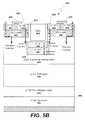
- FIG. 5Ais a schematic cross-sectional diagram of the IGBT of FIG. 4 .
- FIG. 5Bis a schematic cross-sectional diagram of a modified version of the of the IGBT of FIG. 5A .
- FIGS. 6A and 6Bare cross-sectional diagrams that illustrate the simulated electrical field intensity (at a substrate voltage of 1200 volts) for both the power MOSFET having the structure of FIG. 1 and a MOSFET according to embodiments of the present invention having the structure of FIG. 2A .
- FIGS. 7A and 7Bare graphs showing the simulated electrical field distributions along the cross section of the silicon carbide UMOSFET of FIG. 6A and the UMOSFET according to embodiments of the present invention of FIG. 6B , respectively.
- FIGS. 8A-8Gare schematic cross-sectional diagrams illustrating methods of forming a UMOSFET according to certain embodiments of the present invention.
- FIGS. 9A-9Eillustrate a method of forming a p-type silicon layer in the bottom of a gate trench according to certain embodiments of the present invention.
- FIGS. 10A-10Cillustrate a method of forming a p-type silicon layer in the bottom of a gate trench according to further embodiments of the present invention.
- first and secondare used herein to describe various regions, layers and/or elements, these regions, layers and/or elements should not be limited by these terms. These terms are only used to distinguish one region, layer or element from another region, layer or element. Thus, a first region, layer or element discussed below could be termed a second region, layer or element, and similarly, a second region, layer or element may be termed a first region, layer or element without departing from the scope of the present invention.
- Relative termssuch as “lower” or “bottom” and “upper” or “top,” may be used herein to describe one element's relationship to another element as illustrated in the drawings. It will be understood that relative terms are intended to encompass different orientations of the device in addition to the orientation depicted in the drawings. For example, if the device in the drawings is turned over, elements described as being on the “lower” side of other elements would then be oriented on “upper” sides of the other elements. The exemplary term “lower” can, therefore, encompass both an orientation of “lower” and “upper,” depending of the particular orientation of the figure.
- Embodiments of the inventionare described herein with reference to cross-sectional illustrations that are schematic illustrations. As such, variations from the shapes of the illustrations as a result, for example, of manufacturing techniques and/or tolerances, are to be expected. Thus, embodiments of the invention should not be construed as limited to the particular shapes of regions illustrated herein but are to include deviations in shapes that result, for example, from manufacturing. For example, an implanted region illustrated as a rectangle will, typically, have rounded or curved features and/or a gradient of implant concentration at its edges rather than a binary change from implanted to non-implanted region. Thus, the regions illustrated in the figures are schematic in nature and their shapes are not intended to illustrate the actual shape of a region of a device and are not intended to limit the scope of the invention.
- Power silicon carbide MOSFETsare in use today for applications requiring high voltage blocking such as voltage blocking of 5,000 volts or more.
- silicon carbide MOSFETsare commercially available that are rated for current densities of 10 A/cm 2 or more that will block voltages of at least 10 kV.
- a plurality of “unit cells”are typically formed, where each unit cell typically comprises a MOSFET that has a gate electrode, two source regions (one at either side of the gate electrode) and a drain region.
- a large number of these unit cellsare typically provided on a single semiconductor substrate, and a common gate electrode is typically formed on a top side of the semiconductor substrate that acts as the gate electrode for all of the unit cells.
- the opposite (bottom) side of the semiconductor substrateacts as a common drain for all of the units cells of the device.
- a plurality of source regionsare interposed within openings in the gate electrode. These source regions are also electrically connected to each other to serve as a common source. It will be appreciated that the above description is of an n-type MOSFET; the locations of the drain and source would be reversed for a p-type MOSFET.
- embodiments of the present inventionare described with respect to cross-sectional diagrams that show a single unit cell of a power MOSFET. It will be appreciated that actual implementations will typically include a large number of unit cells. However, it will also be appreciated that the present invention is not limited to such devices, and that the claims appended hereto also cover MOSFETs and other power switching devices that comprise, for example, a single unit cell. Moreover, while the present disclosure focuses on silicon carbide devices, it will be appreciated that embodiments of the present invention may also have applicability to devices formed using other wide band-gap semiconductors such as, for example, gallium nitride, zinc selenide or any other II-VI or III-V wide band-gap compound semiconductors.
- other wide band-gap semiconductorssuch as, for example, gallium nitride, zinc selenide or any other II-VI or III-V wide band-gap compound semiconductors.
- FIG. 1is a schematic cross-sectional diagram of an n-channel silicon carbide power UMOSFET 100 .
- the UMOSFET 100may be implemented on a heavily-doped (n + ) single crystal n-type silicon carbide substrate 110 .
- a lightly-doped (n ⁇ )n-type silicon carbide drift layer 120is provided on the substrate 110 .
- a moderately-doped (n) n-type silicon carbide current spreading layer 130is provided on the n ⁇ silicon carbide drift layer 120 .
- the current spreading layer 130may be split into two portions by the gate structure, as is described below.
- the drift layer 120 and the current spreading layer 130may be formed, for example, by epitaxial growth on the substrate 110 .
- the lightly-doped (n ⁇ ) drift layer 120may have a doping concentration of, for example, about 8.5 ⁇ 10 14 dopants per cubic cm, and may be about 50 microns thick (in the vertical direction in FIG. 1 ).
- the moderately-doped n-type current spreading layer 130may have a doping concentration of, for example, about 2.1 ⁇ 10 17 dopants per cubic cm, and may be about 0.4 microns thick.
- First and second spaced apart p-type silicon carbide wells 140 (“p-wells”)are provided on an upper surface of the n-type current spreading layer 140 .
- the p-wells 140may be epitaxially grown or formed by an ion implantation process.
- Each p-well 140may be moderately doped p-type to, for example, a dopant concentration of about 2 ⁇ 10 17 dopants per cubic cm, and each p-well 140 may be about 1 micron thick.
- First and second heavily-doped (n + ) n-type silicon carbide source regions 150are provided within upper portions of the respective p-wells 140 .
- Each heavily-doped region 150may have a dopant concentration of about 6.5 ⁇ 10 18 dopants per cubic cm, and each source region 150 may be about 0.5 microns thick.
- the heavily-doped (n + ) n-type silicon carbide regions 150act as the source of the MOSFET 100 , while the current spreading layer 130 , the drift layer 120 and the substrate 110 act as a common drain region for the MOSFET 100 .
- Channel regions 145are provided in each p-well 130 between the source region 150 and the current spreading layer 130 .
- a gate insulating layer 170that may have, for example, a generally U-shape is formed on the drift layer 120 between the two portions of the current spreading layer 130 and the two p-wells 140 .
- the gate insulating layer 170may comprise, for example, a thin silicon dioxide layer.
- a gate electrode 160is provided on the gate insulating layer 170 .
- the gate electrode 160may comprise, for example, a doped polysilicon or silicon carbide layer, and it may fill the interior of the U-shaped gate insulating layer 170 .
- the gate insulating layer 170 and the gate electrode 160together comprise a gate trench structure 175 .
- a heavily-doped (p + ) p-type silicon carbide region 180is provided beneath the gate electrode 160 underneath the gate trench structure 175 .
- the heavily-doped (p + ) p-type silicon carbide region 180may be formed by ion implantation, and is electrically connected to the source regions 150 by an electrical connection (not shown in FIG. 1 ).
- the p-type region 180may also be considered to be part of the gate trench structure 175 .
- An ohmic contact 185(e.g., a metal layer) is provided on the n + source regions 150 and on an upper portion of the p-wells 140 .
- the contacts 185may be electrically connected to each other and may act as a common source contact for the MOSFET 100 .
- An ohmic contact 190 on the back side of the n + silicon carbide substrate 110acts as the drain contact for the MOSFET 100 .
- UMOSFETs such as MOSFET 100may typically be fabricated with fewer photolithographic and ion implantation steps as compared to DMOSFETs, and hence may be less expensive to manufacture and/or may exhibit higher device yields. Additionally, the channel mobility of UMOSFETs may be as much as five or more times greater than the channel mobility of a similar DMOSFET due to the lower on-state resistance provided by the vertical structure of the UMOSFET. UMOSFETs may also have higher channel densities than comparable DMOSFETs. Unfortunately, the p-type region 180 underneath the gate trench may increase the JFET resistance of the device, and increases the depth of the trench structure 175 .
- the increased JFET resistance in the p-type region 180may negatively impact the switching speed of the MOSFET.
- power UMOSFETsmay suffer from electrical field crowding at the corners of the insulating layer 170 at the bottom of the trench structure 175 . This electrical field crowding can damage the gate insulation layer 170 and/or decrease manufacturing yields.
- Electron mobilities in the inversion layer in the channels 145 of greater than 150 cm 2 /Vshave been demonstrated in UMOSFET devices formed on (112 ⁇ 0) face (A-face) of 4H silicon carbide, which is much higher than the electron channel mobilities that are currently achievable on the Si face of 4H silicon carbide.
- A-face 4H silicon carbideis typically not preferred in vertical power devices due to the lower critical field of this material in the (0001) direction.
- power switching devicesthat include MOSFETs are provided such as, for example, power MOSFET switches, power insulated gate bipolar junction transistors (“IGBTs”) and power MOS-controlled thyristors (MCTs) that are have a novel UMOSFET structure.
- MOSFET switchespower MOSFET switches
- IGBTspower insulated gate bipolar junction transistors
- MCTspower MOS-controlled thyristors
- the corners of the MOS trench structureare protected by a semiconductor material that has a lower sheet resistance (e.g., silicon) than an underlying wide band-gap (e.g., silicon carbide) semiconductor drift layer.
- the silicon and the underlying silicon carbideform a heterojunction.
- the siliconmay be heavily doped (p + ) p-type silicon, while in a p-channel device, the silicon may be heavily doped (n + ) n-type silicon.
- the silicon regionmay be electrically connected to the source regions of an n-channel UMOSFET, and to the drain regions of a p-channel UMOSFET.
- the UMOSFETs according to embodiments of the present inventionmay exhibit very fast switching speeds.
- the JFET resistance due to the introduction of the heterojunctionmay be minimal since the built-in potential of such a junction is only about 1.5 volts, which is significantly less than the built-in potential of a silicon carbide homojunction, which exceeds 2.7 volts.
- the heavily-doped p-type silicon regioncan be formed and doped during growth of the device, and hence does not significantly impact the cost of manufacturing the device.
- the power MOSFET based devices according to embodiments of the present inventionmay exhibit a number of advantages as compared to conventional devices. For example, when the devices according to embodiments of the present invention are in their reverse-biased or “off-states,” the silicon/silicon carbide heterojunction expands the depletion region, thereby shielding the electrical field from the corners of the trench structure.
- the resulting lower electric field levels in the gate oxide layerreduces the stress experienced by the gate oxide layer as compared to conventional UMOSFETs, and thus may have improved device stability. As the gate oxide may undergo less stress during device operation, the standard for qualifying a device may also be lowered, which may result in improved device manufacturing yields.
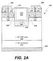
- FIG. 2Ais a schematic cross-sectional diagram of a power MOSFET 200 according to certain embodiments of the present invention.
- the MOSFET 200may be implemented as a monolithic device on, for example, a heavily-doped bulk single crystal n-type silicon carbide substrate 210 . It will be appreciated, however, that, in some embodiments, the substrate 210 may be removed after the device is formed, or may be omitted altogether. It will also be appreciated that herein the term “substrate” may encompass a semiconductor layer such as, for example, a semiconductor layer that is epitaxially grown or otherwise formed on a semiconductor or non-semiconductor substrate.
- a lightly-doped (n ⁇ ) silicon carbide drift layer 220is provided on the substrate 210 .
- the drift layer 220may be formed, for example, by epitaxial growth on the substrate 210 .
- a moderately-doped (n) n-type silicon carbide current spreading layer 230is provided on the n ⁇ silicon carbide drift layer 220 .
- the current spreading layer 230may be split into two portions by the gate structure (the gate structure is described below).
- First and second spaced apart p-type silicon carbide wells 240 (“p-wells”)are provided on an upper surface of the n-type silicon carbide current spreading layer 230 .
- the p-wells 240may be epitaxially grown or formed by an ion implantation process.
- First and second heavily-doped (n + ) n-type silicon carbide regions 250are provided within upper portions of the respective p-wells 240 . Additionally, upper portions 242 of each p-well 240 that are adjacent the respective first and second heavily-doped (n + ) n-type silicon carbide regions 250 are heavily-doped (p + ) p-type.
- a generally U-shaped gate insulating layer 270(e.g., a silicon dioxide layer) is formed on the drift layer 220 between the p-wells 240 .
- a gate electrode 260(e.g., a doped polysilicon or silicon carbide layer) is provided on the gate insulating layer 270 .
- the gate electrode 260may fill the interior of the U-shaped gate insulating layer 270 .
- the gate insulating layer 270 and the gate electrode 260together comprise a gate trench structure 275 .
- a heavily-doped (p + ) p-type silicon region 280is provided beneath the gate electrode 260 underneath the bottom portion of the gate insulating layer 270 .
- the heavily-doped (p + ) p-type silicon region 280is electrically connected to the regions 250 by an electrical connection (not shown in FIG. 2A ).
- the heavily-doped (p + ) p-type silicon region 280forms a heterojunction with the underlying n ⁇ silicon carbide drift layer 220 .
- the p-type region 280may also be considered to be part of the gate trench structure 275 .
- the heavily-doped (n + ) n-type silicon carbide regions 250act as the source of the MOSFET 200 , while the drift layer 220 acts as a common drain region for the MOSFET 200 .
- Channel regions 245are provided in each p-well 240 between the source region 250 and the current spreading layer 230 .
- An ohmic contact 285(e.g., a metal layer) is provided on the n + source regions 250 and on the upper portions of the p-wells 240 .
- the contacts 285may be electrically connected to each other and may act as a common source contact for the MOSFET 200 .
- An ohmic contact 290 on the back side of the n + silicon carbide substrate 210acts as the drain contact for the MOSFET 200 .
- the current spreading layer 230acts to spread out the current flowing through the p-wells 240 . If the current spreading layer 230 is not provided, it may be necessary to significantly increase the vertical spacing between the top surface of the heavily-doped p-type silicon layer 280 and the bottom surface of the p-wells 240 . The degree of separation necessary is a function of (1) the built-in potentials between the p-wells 240 and drift layer 220 (or the current spreading layer 230 ) and (2) the built-in potentials between the heavily-doped region 280 at the bottom of the trench structure and the drift layer 220 . When the heavily-doped region comprises a silicon carbide layer as is in the case of the MOSFET 100 of FIG.
- the vertical spacing between the top surface of the heavily-doped region 180 and the bottom surface of the p-wells 140may need to be on the order of 5 microns or more for various applications, resulting in a significantly taller device structure, that is more expensive to manufacture.
- the heavily-doped region at the bottom of the trench structurecomprises a silicon layer that forms heterojunction with the drift layer 220 as is in the case of the MOSFET 200 of FIG. 2A
- the built in potential of the second junctionmay be reduced from greater than 2.5 volts in the case of the device 100 of FIG. 1 to approximately 1.5 volts for the device of FIG. 2A .
- the vertical spacing between the top surface of the heavily-doped silicon region 280 and the bottom surface of the p-wells 240 in the MOSFET 200 of FIG. 2Amay need to only be on the order of perhaps 3 microns.
- p + and n + conductivity type regions and epitaxial layers described abovemay be as heavily doped as possible without causing excessive fabrication defects.
- Suitable dopants for producing the p-type silicon carbide regionsinclude aluminum, boron or gallium.
- Suitable dopants for producing the n-type silicon carbide regionsinclude nitrogen and phosphorus.
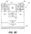
- FIG. 2Bis a schematic cross-sectional diagram of a power MOSFET 200 ′ according to further embodiments of the present invention.
- the MOSFET 200 ′may be identical to the MOSFET 200 of FIG. 2A , except that it further includes an implanted p-type silicon carbide region 282 between the heavily-doped (p + ) p-type silicon region 280 and the n ⁇ silicon carbide drift layer 220 .
- the p-type silicon layermay form a Schottky contact to the n ⁇ silicon carbide drift layer 220 .
- Such Schottky contactsmay exhibit increased leakage currents.
- the p-n junction formed between the p-type silicon carbide layer 282 and the n-type silicon carbide layer 220may comprise an ohmic contact, and hence may exhibit reduced leakage currents. This may be advantageous, for example, in devices that are designed for high temperature applications where leakage current problems may be exacerbated.
- FIG. 3Ais a schematic cross-sectional diagram of a power MOSFET 300 according to further embodiments of the present invention.
- the MOSFET 300may be implemented as a monolithic device on, for example, a heavily-doped bulk single crystal n-type silicon carbide substrate 310 . It will be appreciated, however, that, in some embodiments, the substrate 310 may be removed after the device is formed, or may be omitted altogether.
- a lightly-doped (n ⁇ ) silicon carbide drift layer 320is provided on the substrate 310 .
- the drift layer 320may be formed, for example, by epitaxial growth on the substrate 310 .
- a moderately-doped n-type silicon carbide current spreading layer 330is provided on the n ⁇ silicon carbide drift layer 320 .
- the current spreading layer 330may be split into two portions by the gate structure, as is described below.
- First and second spaced apart p-type silicon carbide wells 340 (“p-wells”)are provided on an upper surface of the moderately-doped n-type silicon carbide current spreading layer 330 .
- the p-wells 340may be epitaxially grown or formed by an ion implantation process, and may be moderately-doped.
- First and second heavily-doped (n + ) n-type silicon carbide source regions 350are provided within upper portions of the respective p-wells 340 .
- upper portions 342 of each p-well 340 that are adjacent the respective first and second heavily-doped (n + ) n-type silicon carbide source regions 350are heavily-doped p-type.
- Channel regions 345are provided in each p-well 340 between the source region 350 and the current spreading layer 330 .
- a gate insulating layer 370(e.g., a silicon dioxide layer) is formed on the drift layer 320 between the p-wells 340 .
- the gate insulating layer 370may have an upside down “U” shape, with a pair of recesses provided that each start at the bottom of the “U” shape (i.e., the top of the layer 370 in the orientation of FIG. 3A ) and run most of the way through the legs of the upside down “U” shape.
- a gate electrode 360e.g., a doped polysilicon or silicon carbide layer
- the gate insulating layer 370 and the gate electrode 360together comprise a gate trench structure 375 .
- a heavily-doped (p + ) p-type silicon region 380is provided in the interior of the upside down “U” shaped gate insulating layer 370 .
- This heavily-doped (p + ) p-type silicon region 380is electrically connected to the source regions 350 by an electrical connection (not shown in FIG. 3A ).
- the heavily-doped (p + ) p-type silicon region 380forms a heterojunction with the underlying n ⁇ silicon carbide drift layer 320 .
- the heavily-doped (n + ) n-type silicon carbide source regions 350act as the source of the MOSFET 300 , while the drift layer 320 acts as a common drain region for the MOSFET 300 .
- An ohmic contact 385(e.g., a metal layer) is provided on the n + source regions 350 and on the p + regions 342 . The contacts 385 may be electrically connected to each other and may act as a common source contact for the MOSFET 300 .
- An ohmic contact 390 on the back side of the n + silicon carbide substrate 310acts as the drain contact for the MOSFET 300 .
- p + and n + conductivity type regions and epitaxial layers described abovemay be as heavily doped as possible without causing excessive fabrication defects.
- Suitable dopants for producing the p-type silicon carbide regionsinclude aluminum, boron or gallium.
- Suitable dopants for producing the n-type silicon carbide regionsinclude nitrogen and phosphorus.
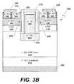
- FIG. 3Bis a schematic cross-sectional diagram of a power MOSFET 300 ′ according to further embodiments of the present invention.
- the MOSFET 300 ′may be identical to the MOSFET 300 of FIG. 3A , except that it further includes an implanted p-type silicon carbide region 382 between the heavily-doped (p + ) p-type silicon region 380 and the n ⁇ silicon carbide drift layer 320 .
- the p-type silicon layerforms a Schottky contact to the n ⁇ silicon carbide drift layer 320 .
- Such Schottky contactsmay exhibit increased leakage currents.
- the p-n junction formed between the p-type silicon carbide layer 382 and the n-type silicon carbide layer 320may comprise an ohmic contact, and hence may exhibit reduced leakage currents.
- FIGS. 2A , 2 B, 3 A and 3 Beach illustrate the structure of a unit cell of an n-channel MOSFET, it will be appreciated that pursuant to further embodiments of the present invention, the polarity of each of the semiconductor layers in each device could be reversed so as to provide corresponding p-channel MOSFETs.
- an IGBTis a device that combines the high impedance gate of the power MOSFET with the small on-state conduction losses of a power BJT.
- An IGBTmay be implemented, for example, as a Darlington pair that includes a high voltage n-channel MOSFET at the input and a BJT at the output. The MOSFET supplies the base current of the BJT. Since IGBTs are voltage controlled devices, they present minimal load to external drive circuits, yet have the high current density switching characteristics of a BJT.
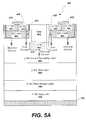
- FIG. 4is a simplified circuit diagram of a p-channel silicon carbide power IGBT 400 that includes a UMOSFET according to embodiments of the present invention.
- FIG. 5Ais a schematic cross-sectional diagram of the IGBT 400 of FIG. 4 .
- the IGBT 400includes an NPN silicon carbide power BJT 410 that has a base, an emitter and a collector.
- the IGBT 400further includes a silicon carbide power MOSFET 420 having a gate, a source and a drain.
- the source of the silicon carbide power MOSFET 420is electrically connected to the base of the silicon carbide power BJT 410
- the drain of the silicon carbide power MOSFET 420is electrically connected to the collector of the silicon carbide power BJT 410 .
- the collector of the BJT 410is the emitter 404 of the IGBT 400
- the emitter of the BJT 410is the collector 406 of the IGBT 400
- the gate of the MOSFET 420is the gate 402 of the IGBT 400 .
- the IGBT 400may operate as follows.
- An external drive circuitis connected to the gate 402 of the IGBT 400 for applying a gate bias voltage to the power MOSFET 420 .
- this external drive circuitapplies a voltage to the gate 402 of IGBT 400 that is greater than the threshold voltage of the MOSFET 420 , an inversion layer is formed under the gate 402 which acts as a channel 428 that electrically connects the p + emitter 404 of the IGBT 400 to the base of BJT 410 .
- Holesare injected from the p + emitter region 404 through the channel 428 into the base of BJT 410 . This hole current acts as the base current that drives the BJT 410 .
- the silicon carbide power MOSFET 420converts the silicon carbide power BJT 410 from a current driven device to a voltage driven device, which may allow for a simplified external drive circuit.
- the silicon carbide power MOSFET 420acts as a driver transistor, and the silicon carbide power BJT 410 acts as the output transistor of the IGBT 400 .
- FIG. 5Ais a schematic cross-sectional diagram of the IGBT 400 of FIG. 4 . It will be appreciated that to form the power IGBT 400 , the structure shown in FIG. 5A would typically comprise a single unit cell, of the IGBT 400 , and a plurality of these unit cells would be implemented in parallel. To simplify the discussion below, it will be assumed that the IGBT 400 of FIG. 4 is implemented as the single unit cell illustrated in FIG. 5A .
- the IGBT 400may be formed on, for example, a heavily-doped single crystal n-type silicon carbide substrate 406 .
- This n + substrateacts as the collector 406 of the IGBT 400 (and hence also as the emitter of the BJT 410 ).
- a p + silicon carbide field stopper layer 445is provided on the substrate 406 .
- a lightly p-type doped (p ⁇ ) silicon carbide drift layer 450is provided on the field stopper layer 445 .
- a moderately-doped p-type silicon carbide current spreading layer 455is provided on the drift region 450 .
- the p-type silicon carbide layers 445 , 450 , 455act as the base of the BJT 410 and as the source region of the MOSFET 420 .
- a pair of silicon carbide n-wells 460are provided in an upper surface of the p-type silicon carbide current spreading layer 455 .
- a p + silicon carbide drain region 442is formed in an upper portion of each n-well 460 . This p + silicon carbide drain region 442 acts as a common drain for the IGBT 400 .
- a heavily-doped n + silicon carbide emitter region 404(which also acts as the collector of the BJT 410 ) is formed in the upper portion of each n-well 460 adjacent the p + silicon carbide drain region 442 .
- An ohmic contact 475is formed to contact the n + silicon carbide emitter region 404 and the p + silicon carbide drain region 442 , and an ohmic contact 480 is formed on the back side of the n + silicon carbide substrate 406 .
- a “U” shaped gate insulating layer 470such as a silicon dioxide layer is formed on the p-type silicon carbide current spreading layer 455 and on sidewalls of the n-wells 460 .
- a gate electrode 402such as, for example, a silicon carbide layer is formed on the gate insulating layer 470 that acts as the gate 402 of the IGBT 400 .
- the gate electrode 402may fill the interior of the insulating layer 470 .
- a channel 428 of the MOSFET 420is thereby defined in each of the n-wells 460 between the p + drain region 442 and the p-type current spreading layer 455 .
- the gate insulating layer 470 and the gate electrode 460together comprise a gate trench structure 476 .
- a heavily-doped (n + ) n-type silicon region 490is provided beneath the gate electrode 402 underneath the bottom portion of the gate insulating layer 370 .
- the heavily-doped (n + ) n-type silicon region 490is electrically connected to the n-type silicon carbide emitter regions 404 by an electrical connection (not shown in FIG. 5A ).
- the heavily-doped (n + ) n-type silicon region 490forms a heterojunction with the underlying p-type silicon carbide current spreading layer 455 .
- FIG. 5Bis a schematic cross-sectional diagram of an IGBT 400 ′ according to further embodiments of the present invention.
- the IGBT 400 ′may be identical to the IGBT 400 of FIG. 5A , except that it further includes a heavily-doped n-type silicon carbide region 492 between the heavily-doped (n + ) n-type silicon region 490 and the p-type silicon carbide current spreading layer 455 .
- a p-n junctionmay be formed between the n + silicon region 490 and the current spreading layer 455 as opposed to a Schottky contact as is the case in the device of FIG. 5A , and thus the device of FIG. 5B may exhibit reduced leakage currents.
- FIGS. 5A and 5Beach illustrate the structure of a p-channel IGBT, it will be appreciated that pursuant to further embodiments of the present invention, the polarity of each of the semiconductor layers in each device could be reversed so as to provide corresponding n-channel IGBTs according to further embodiments of the present invention.
- the power MOSFETs and IGBTs and other deviceswhich include, for example, a silicon/silicon carbide heterojunction underneath the gate trench, may shield the off-state electrical field from the corners of the trench structure, which may improve both device stability and/or manufacturing yields.
- IGBTsmay include a parasitic thyristor.
- a voltage differenceappears across the p-n junction formed by each well region and its associated drain region (e.g., n-well 460 and p-type drain region 442 of FIGS. 5A and 5B ). Once this voltage difference reaches a threshold amount (e.g., about 2.7 volts in a typical silicon carbide IGBT), the p-n junction formed between the well region and the drain region of the device turns on. Once this has occurred, the current will continue to flow from the emitter to the collector even if the bias voltage that is applied to the gate is removed.
- a threshold amounte.g., about 2.7 volts in a typical silicon carbide IGBT
- the IGBTcan only be used at current densities that are less than the current density required to turn on the well region-drain region p-n junction, as once that threshold current density is reached, the ability to use the gate electrode of the IGBT to control the current flow through the device is lost.
- This conditionis commonly referred to as “latch-up” of the parasitic thyristor, and when it occurs, it usually leads to the destruction of the device. Consequently, care must be taken to limit the on-state current densities through an IGBT in order to avoid latch-up of the parasitic thyristor.
- silicon-based IGBTshave limitations in terms of controllable current density, electron mobility in silicon is typically 2-3 times the hole mobility, whereas in the drift region of a 4H—SiC-based IGBT, the electron mobility will typically be more than 10 times the hole mobility.
- silicon carbide IGBTsthe vast majority of the current comprises electron current.
- silicon carbide IGBTsare inherently more prone to latch-up than are silicon-based IGBTs because the current flowing through the well regions that cause this latch up builds more quickly due to the pronounced difference in electron and hole mobilities in silicon carbide.
- n-type silicon layer 490may act as a minority carrier diversion path or “minority carrier diverter.”
- the silicon layer 490may provide a conduction path that may carry a significant percentage (e.g., 50 percent) of the minority carrier current through the device, thereby reducing the current flow through the well region-drain region p-n junction so as to allow larger on-state current densities without latch-up of the parasitic thyristor. Consequently, the silicon carbide IGBTs according to embodiments of the present invention may have increased controllable current densities.
- the heavily-doped n-type silicon layer 490also reduces the degree to which the gate electrode 402 directly overlaps the p-type current spreading layer 455 through the gate insulating layer 470 .
- the IGBTs according to embodiments of the present inventionmay provide increased switching speed.
- FIGS. 6A and 6Bare cross-sectional diagrams that illustrate the simulated electrical field intensity (at a substrate voltage of 1200 volts) for both the power MOSFET having the structure of FIG. 1 and a MOSFET according to embodiments of the present invention having the structure of FIG. 2A .
- FIGS. 7A and 7Bare graphs showing the simulated electrical field distributions along the cross section of the silicon carbide UMOSFET of FIG. 6A and the UMOSFET according to embodiments of the present invention of FIG. 6B .
- the electric field under the gate electrodehas a value exceeding 4.5 ⁇ 10 6 V/cm in the middle portion of the drift region 120 under the gate electrode, and electric field spikes to a value of approximately 6.5 ⁇ 10 6 V/cm at each corner of the trench structure.
- the electric fieldis nearly eliminated under the gate electrode, and the electric field is reduced under the p-wells 240 as well.
- FIGS. 8A-8Gillustrate a method of forming a silicon carbide UMOSFET having a silicon-silicon carbide heterojunction under the gate trench according to some embodiments of the present invention.
- operationsmay begin with the formation of a lightly-doped n-type silicon carbide drift layer 505 on an n-type silicon carbide substrate 500 .
- a p-type silicon carbide layer 510may be formed on top of the drift layer 505 that will be used to form p-wells in subsequent processing steps.
- a heavily-doped n-type silicon carbide layer 515may be formed on top of the p-type silicon carbide layer 510 .
- the layers 505 , 510 and 515may all be grown via epitaxial growth in a growth reactor, and the resulting structure may be removed from the growth reactor for subsequent processing.
- a trench 520may be formed that penetrates the heavily-doped n-type silicon carbide layer 515 , the p-type silicon carbide layer 510 and an upper portion of the n-type silicon carbide drift layer 505 .
- This trenchmay be formed by forming a mask layer (not shown) on the upper surface of the heavily-doped n-type silicon carbide layer 515 , using a photolithography process to pattern the mask to expose the area where the trench 520 is to be formed, and then performing an anisotropic etching process to selectively etch the device, thereby forming the trench 520 .
- the mask layer(not shown) may then be removed.
- another maskmay then be formed on an upper surface of the device and patterned to expose areas where heavily-doped p-type regions 525 are to be formed.
- An ion implantation processmay then be performed to implant p-type dopants into the heavily-doped p-type regions 525 .
- the structuremay then be annealed at a temperature of, for example, 1600° C. in order to activate the p-type dopants.
- a heavily-doped p-type silicon layer 530may be fanned in the bottom of the trench 520 .
- One possible method of forming this layeris discussed in detail below with reference to FIGS. 9A-9E .
- a gate dielectric film 535may be formed on the upper surface of the device and in the gate trench 520 , including on an upper surface of the silicon layer 530 .
- the gate dielectric filmmay be formed, for example, by performing a heat treatment in an environment that includes oxygen in order to form a silicon dioxide gate dielectric film 535 .
- a polysilicon gate electrode 540is formed in the gate trench 520 .
- the gate electrode 540may be formed in a conventional fashion.
- a passivation layer 545such as, for example, a silicon dioxide layer, is formed on the upper surface of the device.
- the passivation layer 545may be patterned in a conventional fashion, and then a source contact 550 may be formed that contacts the heavily doped n-type source regions 515 and the heavily-doped p-type regions 525 .
- a drain contact 555may be formed on the back side of the silicon carbide substrate 500 to complete fabrication of the device.
- the contacts 550 , 555may comprise, for example, metal contacts.
- FIGS. 9A-9Eillustrate one possible method of forming the heavily-doped p-type silicon layer 530 illustrated in FIGS. 8D-8G above in the bottom of the trench 520 .
- a thin oxide layer 560may be formed on sidewalls and a bottom surface of the gate trench 520 .
- An etch back processsuch as, for example, an anisotropic etch may then be used to remove the portion of the oxide layer 560 that is on the bottom of the gate trench to expose the drift layer 505 .
- a p-type polysilicon layer 530 ′may be formed on the structure and within the gate trench 520 .
- the polysilicon layer 530 ′may grow from the oxide layer 560 that is formed on the sidewalls of the gate trench 520 to fill the gate trench 520 .
- a planarization processsuch as, for example, an etch back process or a chemical-mechanical processing process may be performed to remove the polysilicon from the upper surface of the structure while leaving the polysilicon in the gate trench 520 , thereby converting the polysilicon layer 530 ′ into a polysilicon pattern 530 ′′.
- a thermal oxidization process followed by a BOE (buffered oxide etch) wet etching processmay then be performed to remove a portion of the polysilicon pattern 530 ′′ that is in the gate trench 520 to form the polysilicon region 530 .
- voltage probingmay be performed to determine when a sufficient amount of the polysilicon pattern 530 ′′ has been removed such that an upper surface of the polysilicon pattern 530 ′′ is below a lower surface of the p-type silicon carbide layer 510 .
- the p-well 510may be left exposed and a first probe may contact the p-well 510 in this exposed region.
- Another probemay contact the polysilicon pattern 530 ′′ that is in the gate trench 520 .
- the voltage-current characteristics across the two probesis monitored. So long as the top surface of the polysilicon pattern 530 ′′ is above the bottom surface of the p-wells 510 , the probes will measure across a p-type to p-type interface between the p-well 510 and the p-type polysilicon pattern 530 ′′.
- the probeswill measure across a p-n junction between the n-type drift layer 505 and the p-type polysilicon pattern 530 ′′. This will cause a change in the measured I-V characteristics, and hence the probes may be used to determine when the upper surface of the polysilicon pattern 530 ′′ has been sufficiently etched to be below a lower surface of the p-type silicon carbide layer 510 .
- the polysilicon pattern 530 ′′may be further etched for a small distance (e.g., about 0.3 microns) to make sure that the top surface of the p-type polysilicon pattern 530 ′′ is below the lower surface of the p-type silicon carbide layer 510 . At this point, the etching process is stopped, and the polysilicon pattern 530 ′′ has been converted into the polysilicon region 530 .
- the oxide layer 560 on the sidewalls of the gate trench 520may then be removed by, for example, an isotropic etching process.
- a gate oxide layer 570may be formed on the polysilicon layer 530 and on sidewalls of the gate trench 520 by, for example, heating the structure in an oxygen environment.
- a gate electrode 580may be formed to fill the remainder of the gate trench 520 .
- the gate electrode 580may comprise, for example, a polysilicon layer. It should be noted that the method for forming the semiconductor device will also include providing an electrical connection between the polysilicon layer 530 and the source contact 515 .
- FIGS. 8A-9Eillustrate one of way of forming a MOSFET according to embodiments of the present invention, many other methods could be used.
- FIGS. 8A-9Eillustrate a method of forming a UMOSFET according to embodiments of the present invention, it will be appreciated that the operations disclosed therein may be suitably modified to form other devices such as, for example, the IGBT 400 of FIGS. 4 , 5 A and 5 B.
- FIGS. 10A-10Cillustrate one possible method of forming the gate structure 375 of FIG. 3A .
- the operations shown in FIGS. 10A-10Cmay begin after the operations shown in FIG. 8C and may replace the operations illustrated with respect to FIGS. 8D-8F .
- a thin oxide layer 561may be formed on sidewalls and a bottom surface of the gate trench 520 .
- An etch back processsuch as, for example, an anisotropic etch may then be used to remove the portion of the oxide layer 561 (not shown in FIG. 10A ) that is on the bottom of the gate trench to expose the drift layer 505 .
- a p-type polysilicon layer(not shown) may be formed on the structure and within the gate trench 520 . The polysilicon layer may grow from the oxide layer 561 that is formed on the sidewalls of the gate trench 520 to fill the gate trench 520 .
- a planarization processsuch as, for example, an etch back process may be performed to remove the polysilicon from the upper surface of the structure and from an upper portion of the gate trench 520 , thereby converting the polysilicon layer into a polysilicon pattern 531 .
- a planarization processsuch as, for example, an etch back process may be performed to remove the polysilicon from the upper surface of the structure and from an upper portion of the gate trench 520 , thereby converting the polysilicon layer into a polysilicon pattern 531 .
- a wet etching processmay then be performed on the oxide layer 561 on the sidewalls of the gate trench 520 to form trenches 562 in the oxide layer 561 .
- These trenches 562may be formed by, for example, an anisotropic etching process.
- an oxide layer 563may be formed on the surface of the polysilicon pattern 531 .
- a gate electrode 581may be formed in each trench 562 and on top of the oxide layer 563 .
- the gate electrode 581may comprise, for example, a polysilicon layer. It should be noted that the method for forming the semiconductor device will also include providing an electrical connection between the polysilicon pattern 531 and the source contact 515 .
Landscapes
- Electrodes Of Semiconductors (AREA)
Abstract
Description
Claims (49)
Priority Applications (2)
| Application Number | Priority Date | Filing Date | Title |
|---|---|---|---|
| US12/761,518US8415671B2 (en) | 2010-04-16 | 2010-04-16 | Wide band-gap MOSFETs having a heterojunction under gate trenches thereof and related methods of forming such devices |
| PCT/US2011/031150WO2011130044A1 (en) | 2010-04-16 | 2011-04-05 | Wide band-gap mosfets having a heterojunction under gate trenches thereof and related methods of forming such devices |
Applications Claiming Priority (1)
| Application Number | Priority Date | Filing Date | Title |
|---|---|---|---|
| US12/761,518US8415671B2 (en) | 2010-04-16 | 2010-04-16 | Wide band-gap MOSFETs having a heterojunction under gate trenches thereof and related methods of forming such devices |
Publications (2)
| Publication Number | Publication Date |
|---|---|
| US20110254010A1 US20110254010A1 (en) | 2011-10-20 |
| US8415671B2true US8415671B2 (en) | 2013-04-09 |
Family
ID=44787579
Family Applications (1)
| Application Number | Title | Priority Date | Filing Date |
|---|---|---|---|
| US12/761,518Active2031-06-17US8415671B2 (en) | 2010-04-16 | 2010-04-16 | Wide band-gap MOSFETs having a heterojunction under gate trenches thereof and related methods of forming such devices |
Country Status (2)
| Country | Link |
|---|---|
| US (1) | US8415671B2 (en) |
| WO (1) | WO2011130044A1 (en) |
Cited By (18)
| Publication number | Priority date | Publication date | Assignee | Title |
|---|---|---|---|---|
| US20130023096A1 (en)* | 2011-07-11 | 2013-01-24 | Purtell Robert J | Single crystal u-mos gates using microwave crystal regrowth |
| US20130146893A1 (en)* | 2010-09-14 | 2013-06-13 | Taiwan Semiconductor Manufacturing Company, Ltd. | Sic crystalline on si substrates to allow integration of gan and si electronics |
| US20130221429A1 (en)* | 2012-02-29 | 2013-08-29 | Robert Kuo-Chang Yang | Method and apparatus related to a junction field-effect transistor |
| US20140210008A1 (en)* | 2013-01-30 | 2014-07-31 | Mitsubishi Electric Corporation | Semiconductor device and method of manufacturing the same |
| US20150041886A1 (en)* | 2013-08-08 | 2015-02-12 | Cree, Inc. | Vertical power transistor device |
| US20150214047A1 (en)* | 2014-01-29 | 2015-07-30 | Renesas Electronics Corporation | Method for Manufacturing Semiconductor Device |
| US9343383B2 (en)* | 2012-03-02 | 2016-05-17 | Cree, Inc. | High voltage semiconductor devices including electric arc suppression material and methods of forming the same |
| US9397231B2 (en) | 2013-09-03 | 2016-07-19 | Samsung Electronics Co., Ltd. | Semiconductor device having depletion region for improving breakdown voltage characteristics |
| DE102015122833A1 (en)* | 2015-12-23 | 2017-06-29 | Infineon Technologies Ag | Method for producing a semiconductor device |
| US20180138273A1 (en)* | 2016-11-15 | 2018-05-17 | Fuji Electric Co., Ltd. | Silicon carbide semiconductor device and method of manufacturing silicon carbide semiconductor device |
| US20180166530A1 (en)* | 2016-12-08 | 2018-06-14 | Cree, Inc. | Power semiconductor devices having gate trenches and buried edge terminations and related methods |
| US20180182887A1 (en)* | 2016-12-28 | 2018-06-28 | Fuji Electric Co., Ltd. | Silicon carbide semiconductor device and method of manufacturing silicon carbide semiconductor device |
| KR20190001233A (en) | 2017-06-27 | 2019-01-04 | 한국전기연구원 | Trench gate type silicon carbide MOSFET structure and manufacturing method thereof |
| US10276730B2 (en)* | 2016-11-14 | 2019-04-30 | 3-5 Power Electronics GmbH | Stacked Schottky diode |
| US10600903B2 (en) | 2013-09-20 | 2020-03-24 | Cree, Inc. | Semiconductor device including a power transistor device and bypass diode |
| US10797170B2 (en) | 2018-10-05 | 2020-10-06 | Hyundai Motor Company | Semiconductor device and manufacturing method thereof |
| US10868169B2 (en) | 2013-09-20 | 2020-12-15 | Cree, Inc. | Monolithically integrated vertical power transistor and bypass diode |
| US20220052177A1 (en)* | 2014-11-18 | 2022-02-17 | Rohm Co., Ltd. | Semiconductor device and method for manufacturing semiconductor device |
Families Citing this family (67)
| Publication number | Priority date | Publication date | Assignee | Title |
|---|---|---|---|---|
| DE102009028049B3 (en)* | 2009-07-28 | 2011-02-24 | Infineon Technologies Ag | Power semiconductor device with potential probe, power semiconductor device with a power semiconductor device having a potential probe and method for operating a power semiconductor device with a potential probe |
| JP5498431B2 (en)* | 2011-02-02 | 2014-05-21 | ローム株式会社 | Semiconductor device and manufacturing method thereof |
| JP5858934B2 (en) | 2011-02-02 | 2016-02-10 | ローム株式会社 | Semiconductor power device and manufacturing method thereof |
| JP5668576B2 (en)* | 2011-04-01 | 2015-02-12 | 住友電気工業株式会社 | Silicon carbide semiconductor device |
| US20130334501A1 (en)* | 2011-09-15 | 2013-12-19 | The Regents Of The University Of California | Field-Effect P-N Junction |
| WO2013071019A1 (en)* | 2011-11-10 | 2013-05-16 | Rutgers, The State University Of New Jersey | A voltage-gated bipolar transistor for power switching applications |
| EP2602829A1 (en)* | 2011-12-07 | 2013-06-12 | Nxp B.V. | Trench-gate resurf semiconductor device and manufacturing method |
| US8730629B2 (en)* | 2011-12-22 | 2014-05-20 | General Electric Company | Variable breakdown transient voltage suppressor |
| JP2013168540A (en)* | 2012-02-16 | 2013-08-29 | Sumitomo Electric Ind Ltd | Silicon carbide semiconductor device manufacturing method and silicon carbide semiconductor device |
| US9024367B2 (en) | 2012-02-24 | 2015-05-05 | The Regents Of The University Of California | Field-effect P-N junction |
| JP5884617B2 (en)* | 2012-04-19 | 2016-03-15 | 株式会社デンソー | Silicon carbide semiconductor device and manufacturing method thereof |
| JP5751213B2 (en) | 2012-06-14 | 2015-07-22 | 株式会社デンソー | Silicon carbide semiconductor device and manufacturing method thereof |
| JP6264768B2 (en)* | 2012-07-31 | 2018-01-24 | 国立研究開発法人産業技術総合研究所 | Semiconductor structure, semiconductor device, and method of manufacturing the semiconductor structure |
| KR101376892B1 (en)* | 2012-10-29 | 2014-03-20 | 삼성전기주식회사 | Semiconductor device |
| TWI473267B (en)* | 2012-11-06 | 2015-02-11 | Ind Tech Res Inst | Gold oxygen half field effect transistor |
| US9142668B2 (en) | 2013-03-13 | 2015-09-22 | Cree, Inc. | Field effect transistor devices with buried well protection regions |
| US9240476B2 (en) | 2013-03-13 | 2016-01-19 | Cree, Inc. | Field effect transistor devices with buried well regions and epitaxial layers |
| US9012984B2 (en) | 2013-03-13 | 2015-04-21 | Cree, Inc. | Field effect transistor devices with regrown p-layers |
| US9306061B2 (en) | 2013-03-13 | 2016-04-05 | Cree, Inc. | Field effect transistor devices with protective regions |
| US9425153B2 (en) | 2013-04-04 | 2016-08-23 | Monolith Semiconductor Inc. | Semiconductor devices comprising getter layers and methods of making and using the same |
| JP6077385B2 (en)* | 2013-05-17 | 2017-02-08 | トヨタ自動車株式会社 | Semiconductor device |
| US9508841B2 (en)* | 2013-08-01 | 2016-11-29 | General Electric Company | Method and system for a semiconductor device with integrated transient voltage suppression |
| JP6197995B2 (en)* | 2013-08-23 | 2017-09-20 | 富士電機株式会社 | Wide band gap insulated gate semiconductor device |
| WO2015047353A1 (en)* | 2013-09-27 | 2015-04-02 | Intel Corporation | Methods to achieve high mobility in cladded iii-v channel materials |
| WO2015047349A1 (en)* | 2013-09-27 | 2015-04-02 | Intel Corporation | Transistor structure with variable clad/core dimension for stress and band gap modulation |
| US20150263145A1 (en)* | 2014-03-14 | 2015-09-17 | Cree, Inc. | Igbt structure for wide band-gap semiconductor materials |
| US10566192B2 (en)* | 2014-05-07 | 2020-02-18 | Cambridge Electronics, Inc. | Transistor structure having buried island regions |
| US10002941B2 (en) | 2015-05-20 | 2018-06-19 | Fairchild Semiconductor Corporation | Hybrid gate dielectrics for semiconductor power devices |
| DE102015117469A1 (en)* | 2015-10-14 | 2017-04-20 | Infineon Technologies Austria Ag | METHOD FOR PRODUCING A GRABENGATE SEMICONDUCTOR DEVICE THROUGH USING A SCREEN OXIDE LAYER |
| CN109314142B (en)* | 2016-04-07 | 2021-12-17 | 日立能源瑞士股份公司 | Short Channel Trench Power MOSFETs |
| US9793430B1 (en)* | 2016-05-09 | 2017-10-17 | Qatar University | Heterojunction schottky gate bipolar transistor |
| CN106067799B (en)* | 2016-06-13 | 2019-03-05 | 南京芯舟科技有限公司 | A kind of semiconductor devices |
| JP6848316B2 (en)* | 2016-10-05 | 2021-03-24 | 富士電機株式会社 | Semiconductor devices and methods for manufacturing semiconductor devices |
| JP6870286B2 (en)* | 2016-11-15 | 2021-05-12 | 富士電機株式会社 | Manufacturing method of silicon carbide semiconductor device |
| KR20180068211A (en)* | 2016-12-13 | 2018-06-21 | 현대자동차주식회사 | Semiconductor device and method manufacturing the same |
| JP6830627B2 (en)* | 2016-12-22 | 2021-02-17 | 国立研究開発法人産業技術総合研究所 | Semiconductor devices and methods for manufacturing semiconductor devices |
| JP6811118B2 (en)* | 2017-02-27 | 2021-01-13 | 株式会社豊田中央研究所 | MOSFET |
| TWI663725B (en)* | 2017-04-26 | 2019-06-21 | 國立清華大學 | Structure of u-metal-oxide-semiconductor field-effect transistor |
| DE102017207848A1 (en)* | 2017-05-10 | 2018-11-15 | Robert Bosch Gmbh | Vertical power transistor with improved conductivity and high blocking behavior |
| DE102017110508B4 (en)* | 2017-05-15 | 2023-03-02 | Infineon Technologies Ag | Semiconductor device with transistor cells and a drift structure and manufacturing method |
| CN107425071B (en)* | 2017-08-10 | 2019-09-13 | 电子科技大学 | A VDMOS device capable of resisting single-event irradiation |
| JP6729523B2 (en)* | 2017-08-31 | 2020-07-22 | 株式会社デンソー | Silicon carbide semiconductor device and manufacturing method thereof |
| JP6870547B2 (en)* | 2017-09-18 | 2021-05-12 | 株式会社デンソー | Semiconductor devices and their manufacturing methods |
| DE102017220913A1 (en)* | 2017-11-23 | 2019-05-23 | Robert Bosch Gmbh | Vertical power transistor with heterojunction |
| DE102018211825A1 (en)* | 2018-07-17 | 2020-01-23 | Robert Bosch Gmbh | Vertical power transistor and method for manufacturing the vertical power transistor |
| JP7210182B2 (en)* | 2018-07-26 | 2023-01-23 | 株式会社東芝 | Semiconductor devices, inverter circuits, drive devices, vehicles, and elevators |
| CN109768090A (en)* | 2019-02-20 | 2019-05-17 | 重庆大学 | A silicon carbide trench field oxygen power MOS device with built-in heterojunction diode self-protection |
| US10998418B2 (en)* | 2019-05-16 | 2021-05-04 | Cree, Inc. | Power semiconductor devices having reflowed inter-metal dielectric layers |
| CN110571269B (en)* | 2019-08-15 | 2020-10-13 | 西安电子科技大学 | IGBT with partial wide band gap semiconductor material/silicon material heterojunction and manufacturing method thereof |
| JP7532921B2 (en)* | 2020-06-09 | 2024-08-14 | 富士電機株式会社 | Semiconductor Device |
| US11355630B2 (en)* | 2020-09-11 | 2022-06-07 | Wolfspeed, Inc. | Trench bottom shielding methods and approaches for trenched semiconductor device structures |
| TWI801783B (en)* | 2020-12-09 | 2023-05-11 | 大陸商上海瀚薪科技有限公司 | Silicon carbide semiconductor components |
| JP7593114B2 (en)* | 2021-01-05 | 2024-12-03 | 富士電機株式会社 | Method for inspecting silicon carbide semiconductor device |
| US11984499B2 (en)* | 2021-01-11 | 2024-05-14 | Shanghai Hestia Power Inc. | Silicon carbide semiconductor device |
| CN113054030A (en)* | 2021-03-12 | 2021-06-29 | 深圳方正微电子有限公司 | Vertical double-diffusion metal oxide semiconductor transistor and preparation method and application thereof |
| US11677023B2 (en)* | 2021-05-04 | 2023-06-13 | Infineon Technologies Austria Ag | Semiconductor device |
| CN113471276B (en)* | 2021-07-16 | 2025-04-18 | 斯达半导体股份有限公司 | A dual-operating mode silicon carbide power device structure and manufacturing method thereof |
| CN114744044A (en)* | 2022-04-18 | 2022-07-12 | 深圳芯能半导体技术有限公司 | A trench type silicon carbide MOSFET with triple protection gate oxide layer and preparation method thereof |
| CN115101582B (en)* | 2022-06-30 | 2025-09-19 | 电子科技大学 | Groove type SiC MOSFET device |
| US20240047569A1 (en)* | 2022-08-08 | 2024-02-08 | Leap Semiconductor Corp. | Silicon carbide semiconductor power transistor and method of manufacturing the same |
| DE102022209606A1 (en) | 2022-09-14 | 2024-03-14 | Robert Bosch Gesellschaft mit beschränkter Haftung | Vertical GaN power transistor unit cell, vertical GaN power transistor and method of manufacturing a vertical GaN power transistor unit cell |
| TWI854618B (en)* | 2023-04-27 | 2024-09-01 | 世界先進積體電路股份有限公司 | Semiconductor device and fabrication method thereof |
| WO2025076823A1 (en)* | 2023-10-13 | 2025-04-17 | 厦门市三安集成电路有限公司 | Semiconductor testing device, semiconductor wafer, and mobility testing method |
| CN120224754A (en)* | 2023-12-25 | 2025-06-27 | 华润微电子(重庆)有限公司 | A SiC IGBT device and a method for manufacturing the same |
| DE102024202612A1 (en)* | 2024-03-20 | 2025-09-25 | Robert Bosch Gesellschaft mit beschränkter Haftung | Power semiconductor component with smoothed gate-drain capacitance curve |
| CN119743981A (en)* | 2025-03-05 | 2025-04-01 | 杭州谱析光晶半导体科技有限公司 | A SiCVD MOSFET structure with high temperature reliability and its preparation method |
| CN120035157B (en)* | 2025-04-23 | 2025-07-08 | 江苏长晶科技股份有限公司 | A source region doping modulation IGBT structure and preparation method |
Citations (238)
| Publication number | Priority date | Publication date | Assignee | Title |
|---|---|---|---|---|
| US3439189A (en) | 1965-12-28 | 1969-04-15 | Teletype Corp | Gated switching circuit comprising parallel combination of latching and shunt switches series-connected with input-output control means |
| US3629011A (en) | 1967-09-11 | 1971-12-21 | Matsushita Electric Industrial Co Ltd | Method for diffusing an impurity substance into silicon carbide |
| US3924024A (en) | 1973-04-02 | 1975-12-02 | Ncr Co | Process for fabricating MNOS non-volatile memories |
| US4160920A (en) | 1976-07-21 | 1979-07-10 | Bicosa Societe De Recherches | Bistable element and a switch circuit comprising such a bistable element |
| US4242690A (en) | 1978-06-06 | 1980-12-30 | General Electric Company | High breakdown voltage semiconductor device |
| US4466172A (en) | 1979-01-08 | 1984-08-21 | American Microsystems, Inc. | Method for fabricating MOS device with self-aligned contacts |
| US4581542A (en) | 1983-11-14 | 1986-04-08 | General Electric Company | Driver circuits for emitter switch gate turn-off SCR devices |
| EP0176778A2 (en) | 1984-09-28 | 1986-04-09 | Siemens Aktiengesellschaft | Method of producing a pu junction with a high disruptive breakdown voltage |
| US4644637A (en) | 1983-12-30 | 1987-02-24 | General Electric Company | Method of making an insulated-gate semiconductor device with improved shorting region |
| US4811065A (en) | 1987-06-11 | 1989-03-07 | Siliconix Incorporated | Power DMOS transistor with high speed body diode |
| US4875083A (en) | 1987-10-26 | 1989-10-17 | North Carolina State University | Metal-insulator-semiconductor capacitor formed on silicon carbide |
| US4927772A (en) | 1989-05-30 | 1990-05-22 | General Electric Company | Method of making high breakdown voltage semiconductor device |
| EP0372412A1 (en) | 1988-12-06 | 1990-06-13 | Fujitsu Limited | A method for fabricating a semiconductor film which is electrically isolated from substrate |
| US4945394A (en) | 1987-10-26 | 1990-07-31 | North Carolina State University | Bipolar junction transistor on silicon carbide |
| DE3942640A1 (en) | 1988-12-29 | 1990-08-02 | Fuji Electric Co Ltd | Matrix-form MOS device structure - has ring channel layers in each cell and fourth zone symmetric to four cells |
| US4946547A (en) | 1989-10-13 | 1990-08-07 | Cree Research, Inc. | Method of preparing silicon carbide surfaces for crystal growth |
| EP0389863A1 (en) | 1989-03-29 | 1990-10-03 | Siemens Aktiengesellschaft | Process for manufacturing a high-voltage withstanding planar p-n junction |
| US5011549A (en) | 1987-10-26 | 1991-04-30 | North Carolina State University | Homoepitaxial growth of Alpha-SiC thin films and semiconductor devices fabricated thereon |
| US5028977A (en) | 1989-06-16 | 1991-07-02 | Massachusetts Institute Of Technology | Merged bipolar and insulated gate transistors |
| US5032888A (en) | 1989-08-25 | 1991-07-16 | Fuji Electric Co., Ltd. | Conductivity modulation buried gate trench type MOSFET |
| US5111253A (en) | 1989-05-09 | 1992-05-05 | General Electric Company | Multicellular FET having a Schottky diode merged therewith |
| US5155289A (en) | 1991-07-01 | 1992-10-13 | General Atomics | High-voltage solid-state switching devices |
| US5170455A (en) | 1991-10-30 | 1992-12-08 | At&T Bell Laboratories | Optical connective device |
| US5170231A (en) | 1990-05-24 | 1992-12-08 | Sharp Kabushiki Kaisha | Silicon carbide field-effect transistor with improved breakdown voltage and low leakage current |
| US5184199A (en) | 1989-06-07 | 1993-02-02 | Sharp Kabushiki Kaisha | Silicon carbide semiconductor device |
| US5192987A (en) | 1991-05-17 | 1993-03-09 | Apa Optics, Inc. | High electron mobility transistor with GaN/Alx Ga1-x N heterojunctions |
| US5200022A (en) | 1990-10-03 | 1993-04-06 | Cree Research, Inc. | Method of improving mechanically prepared substrate surfaces of alpha silicon carbide for deposition of beta silicon carbide thereon and resulting product |
| US5210051A (en) | 1990-03-27 | 1993-05-11 | Cree Research, Inc. | High efficiency light emitting diodes from bipolar gallium nitride |
| US5270554A (en) | 1991-06-14 | 1993-12-14 | Cree Research, Inc. | High power high frequency metal-semiconductor field-effect transistor formed in silicon carbide |
| US5292501A (en) | 1990-06-25 | 1994-03-08 | Degenhardt Charles R | Use of a carboxy-substituted polymer to inhibit plaque formation without tooth staining |
| EP0615292A1 (en) | 1993-03-10 | 1994-09-14 | Hitachi, Ltd. | Insulated gate bipolar transistor |
| US5348895A (en) | 1992-03-25 | 1994-09-20 | Texas Instruments Incorporated | LDMOS transistor with self-aligned source/backgate and photo-aligned gate |
| US5371383A (en) | 1993-05-14 | 1994-12-06 | Kobe Steel Usa Inc. | Highly oriented diamond film field-effect transistor |
| US5384270A (en) | 1992-11-12 | 1995-01-24 | Fuji Electric Co., Ltd. | Method of producing silicon carbide MOSFET |
| US5385855A (en) | 1994-02-24 | 1995-01-31 | General Electric Company | Fabrication of silicon carbide integrated circuits |
| EP0637069A1 (en) | 1992-06-05 | 1995-02-01 | Cree Research, Inc. | Method of obtaining high quality silicon dioxide passivation on silicon carbide and resulting passivated structures |
| USRE34861E (en) | 1987-10-26 | 1995-02-14 | North Carolina State University | Sublimation of silicon carbide to produce large, device quality single crystals of silicon carbide |
| US5393993A (en) | 1993-12-13 | 1995-02-28 | Cree Research, Inc. | Buffer structure between silicon carbide and gallium nitride and resulting semiconductor devices |
| US5393999A (en) | 1993-02-22 | 1995-02-28 | Texas Instruments Incorporated | SiC power MOSFET device structure |
| US5396085A (en) | 1993-12-28 | 1995-03-07 | North Carolina State University | Silicon carbide switching device with rectifying-gate |
| US5399887A (en) | 1994-05-03 | 1995-03-21 | Motorola, Inc. | Modulation doped field effect transistor |
| US5468654A (en) | 1987-08-19 | 1995-11-21 | Mitsubishi Denki Kabushiki Kaisha | Method of manufacturing an insulated gate bipolar transistor |
| US5473176A (en) | 1993-09-01 | 1995-12-05 | Kabushiki Kaisha Toshiba | Vertical insulated gate transistor and method of manufacture |
| US5479316A (en) | 1993-08-24 | 1995-12-26 | Analog Devices, Inc. | Integrated circuit metal-oxide-metal capacitor and method of making same |
| US5488236A (en) | 1994-05-26 | 1996-01-30 | North Carolina State University | Latch-up resistant bipolar transistor with trench IGFET and buried collector |
| US5506421A (en) | 1992-11-24 | 1996-04-09 | Cree Research, Inc. | Power MOSFET in silicon carbide |
| US5510630A (en) | 1993-10-18 | 1996-04-23 | Westinghouse Electric Corporation | Non-volatile random access memory cell constructed of silicon carbide |
| US5510281A (en) | 1995-03-20 | 1996-04-23 | General Electric Company | Method of fabricating a self-aligned DMOS transistor device using SiC and spacers |
| US5523589A (en) | 1994-09-20 | 1996-06-04 | Cree Research, Inc. | Vertical geometry light emitting diode with group III nitride active layer and extended lifetime |
| US5539217A (en) | 1993-08-09 | 1996-07-23 | Cree Research, Inc. | Silicon carbide thyristor |
| US5545905A (en) | 1993-04-19 | 1996-08-13 | Toyo Denki Seizo Kabushiki Kaisha | Static induction semiconductor device with a static induction schottky shorted structure |
| EP0735591A1 (en) | 1995-03-31 | 1996-10-02 | Consorzio per la Ricerca sulla Microelettronica nel Mezzogiorno - CoRiMMe | Improved DMOS device structure, and related manufacturing process |
| US5587870A (en) | 1992-09-17 | 1996-12-24 | Research Foundation Of State University Of New York | Nanocrystalline layer thin film capacitors |
| US5629531A (en) | 1992-06-05 | 1997-05-13 | Cree Research, Inc. | Method of obtaining high quality silicon dioxide passivation on silicon carbide and resulting passivated structures |
| WO1997039485A1 (en) | 1996-04-15 | 1997-10-23 | Cree Research, Inc. | Silicon carbide cmos and method of fabrication |
| US5710059A (en) | 1996-03-27 | 1998-01-20 | Abb Research Ltd. | Method for producing a semiconductor device having a semiconductor layer of SiC by implanting |
| WO1998002924A2 (en) | 1996-07-16 | 1998-01-22 | Abb Research Ltd. | SiC SEMICONDUCTOR DEVICE COMPRISING A pn JUNCTION WITH A VOLTAGE ABSORBING EDGE |
| US5726463A (en) | 1992-08-07 | 1998-03-10 | General Electric Company | Silicon carbide MOSFET having self-aligned gate structure |
| US5726469A (en) | 1994-07-20 | 1998-03-10 | University Of Elec. Sci. & Tech. Of China | Surface voltage sustaining structure for semiconductor devices |
| US5734180A (en) | 1995-06-02 | 1998-03-31 | Texas Instruments Incorporated | High-performance high-voltage device structures |
| US5739564A (en) | 1992-12-11 | 1998-04-14 | Motorola, Inc. | Semiconductor device having a static-random-access memory cell |
| EP0837508A2 (en) | 1996-10-18 | 1998-04-22 | Hitachi, Ltd. | Semiconductor device and electric power conversion apparatus therewith |
| US5763905A (en) | 1996-07-09 | 1998-06-09 | Abb Research Ltd. | Semiconductor device having a passivation layer |
| US5804483A (en) | 1996-07-11 | 1998-09-08 | Abb Research Ltd. | Method for producing a channel region layer in a sic-layer for a voltage controlled semiconductor device |
| EP0865085A1 (en) | 1997-03-11 | 1998-09-16 | STMicroelectronics S.r.l. | Insulated gate bipolar transistor with high dynamic ruggedness |
| US5831288A (en) | 1996-06-06 | 1998-11-03 | Cree Research, Inc. | Silicon carbide metal-insulator semiconductor field effect transistor |
| US5837572A (en) | 1997-01-10 | 1998-11-17 | Advanced Micro Devices, Inc. | CMOS integrated circuit formed by using removable spacers to produce asymmetrical NMOS junctions before asymmetrical PMOS junctions for optimizing thermal diffusivity of dopants implanted therein |
| US5851908A (en) | 1995-04-10 | 1998-12-22 | Abb Research Ltd. | Method for introduction of an impurity dopant in SiC, a semiconductor device formed by the method and a use of highly doped amorphous layer as a source for dopant diffusion into SiC |
| DE19832329A1 (en) | 1997-07-31 | 1999-02-04 | Siemens Ag | Silicon carbide semiconductor structure manufacturing method |
| US5877041A (en) | 1997-06-30 | 1999-03-02 | Harris Corporation | Self-aligned power field effect transistor in silicon carbide |
| US5877045A (en) | 1996-04-10 | 1999-03-02 | Lsi Logic Corporation | Method of forming a planar surface during multi-layer interconnect formation by a laser-assisted dielectric deposition |
| US5885870A (en) | 1995-11-03 | 1999-03-23 | Motorola, Inc. | Method for forming a semiconductor device having a nitrided oxide dielectric layer |
| US5914500A (en) | 1997-01-21 | 1999-06-22 | Abb Research Ltd. | Junction termination for SiC Schottky diode |
| US5917203A (en) | 1996-07-29 | 1999-06-29 | Motorola, Inc. | Lateral gate vertical drift region transistor |
| US5939763A (en) | 1996-09-05 | 1999-08-17 | Advanced Micro Devices, Inc. | Ultrathin oxynitride structure and process for VLSI applications |
| JPH11238742A (en) | 1998-02-23 | 1999-08-31 | Denso Corp | Method for manufacturing silicon carbide semiconductor device |
| WO1999046809A1 (en) | 1998-03-09 | 1999-09-16 | Harris Corporation | Devices formable by low temperature direct bonding |
| JPH11261061A (en) | 1998-03-11 | 1999-09-24 | Denso Corp | Silicon carbide semiconductor device and method of manufacturing the same |
| US5960289A (en) | 1998-06-22 | 1999-09-28 | Motorola, Inc. | Method for making a dual-thickness gate oxide layer using a nitride/oxide composite region |
| JPH11266017A (en) | 1998-01-14 | 1999-09-28 | Denso Corp | Silicon carbide semiconductor device and method of manufacturing the same |
| US5969378A (en) | 1997-06-12 | 1999-10-19 | Cree Research, Inc. | Latch-up free power UMOS-bipolar transistor |
| US5972801A (en) | 1995-11-08 | 1999-10-26 | Cree Research, Inc. | Process for reducing defects in oxide layers on silicon carbide |
| US5977605A (en) | 1995-08-30 | 1999-11-02 | Asea Brown Boveri Ab | SiC Semiconductor device comprising a pn Junction with a voltage absorbing edge |
| US5976936A (en) | 1995-09-06 | 1999-11-02 | Denso Corporation | Silicon carbide semiconductor device |
| WO1999063591A1 (en) | 1998-05-29 | 1999-12-09 | Conexant Systems, Inc. | Dual-damascene interconnect structures employing low-k dielectric materials |
| US6025233A (en) | 1995-02-08 | 2000-02-15 | Ngk Insulators, Ltd. | Method of manufacturing a semiconductor device |
| US6025608A (en) | 1997-11-13 | 2000-02-15 | Abb Research Ltd. | Semiconductor device of SiC with insulating layer and a refractory metal nitride layer |
| JP2000049167A (en) | 1998-07-31 | 2000-02-18 | Denso Corp | Silicon carbide semiconductor device and method of manufacturing the same |
| US6028012A (en) | 1996-12-04 | 2000-02-22 | Yale University | Process for forming a gate-quality insulating layer on a silicon carbide substrate |
| JP2000082812A (en) | 1998-06-22 | 2000-03-21 | Denso Corp | Silicon carbide semiconductor device and method of manufacturing the same |
| US6048766A (en) | 1998-10-14 | 2000-04-11 | Advanced Micro Devices | Flash memory device having high permittivity stacked dielectric and fabrication thereof |
| JP2000106371A (en) | 1998-07-31 | 2000-04-11 | Denso Corp | Method for manufacturing silicon carbide semiconductor device |
| US6054352A (en) | 1997-02-20 | 2000-04-25 | Fuji Electric Co., Ltd. | Method of manufacturing a silicon carbide vertical MOSFET |
| US6054728A (en) | 1997-04-08 | 2000-04-25 | Fuji Electric Co., Ltd. | Insulated gate thyristor |
| US6063698A (en) | 1997-06-30 | 2000-05-16 | Motorola, Inc. | Method for manufacturing a high dielectric constant gate oxide for use in semiconductor integrated circuits |
| US6083814A (en) | 1998-08-31 | 2000-07-04 | Abb Research Ltd. | Method for producing a pn-junction for a semiconductor device of SiC |
| US6096607A (en) | 1997-08-18 | 2000-08-01 | Fuji Electric Co., Ltd. | Method for manufacturing silicon carbide semiconductor device |
| US6100169A (en) | 1998-06-08 | 2000-08-08 | Cree, Inc. | Methods of fabricating silicon carbide power devices by controlled annealing |
| US6104043A (en) | 1997-01-20 | 2000-08-15 | Abb Research Ltd. | Schottky diode of SiC and a method for production thereof |
| US6107142A (en) | 1998-06-08 | 2000-08-22 | Cree Research, Inc. | Self-aligned methods of fabricating silicon carbide power devices by implantation and lateral diffusion |
| WO2000013236A3 (en) | 1998-08-28 | 2000-08-24 | Cree Research Inc | Layered dielectric on silicon carbide semiconductor structures |
| US6117735A (en) | 1998-01-06 | 2000-09-12 | Fuji Electric Co., Ltd. | Silicon carbide vertical FET and method for manufacturing the same |
| JP2000252478A (en) | 1999-02-26 | 2000-09-14 | Hitachi Ltd | Schottky barrier diode |
| US6121633A (en) | 1997-06-12 | 2000-09-19 | Cree Research, Inc. | Latch-up free power MOS-bipolar transistor |
| US6133587A (en) | 1996-01-23 | 2000-10-17 | Denso Corporation | Silicon carbide semiconductor device and process for manufacturing same |
| US6136727A (en) | 1997-12-19 | 2000-10-24 | Fuji Eletric Co., Ltd. | Method for forming thermal oxide film of silicon carbide semiconductor device |
| US6136728A (en) | 1996-01-05 | 2000-10-24 | Yale University | Water vapor annealing process |
| EP1058317A2 (en) | 1999-06-03 | 2000-12-06 | Intersil Corporation | Low voltage dual-well MOS device |
| US6165822A (en) | 1998-01-05 | 2000-12-26 | Denso Corporation | Silicon carbide semiconductor device and method of manufacturing the same |
| US6180958B1 (en) | 1997-02-07 | 2001-01-30 | James Albert Cooper, Jr. | Structure for increasing the maximum voltage of silicon carbide power transistors |
| US6190973B1 (en) | 1998-12-18 | 2001-02-20 | Zilog Inc. | Method of fabricating a high quality thin oxide |
| US6204203B1 (en) | 1998-10-14 | 2001-03-20 | Applied Materials, Inc. | Post deposition treatment of dielectric films for interface control |
| JP2001085704A (en) | 1999-09-14 | 2001-03-30 | Hitachi Ltd | SiC SCHOTTKY DIODE |
| US6211035B1 (en) | 1998-09-09 | 2001-04-03 | Texas Instruments Incorporated | Integrated circuit and method |
| US6218254B1 (en) | 1999-09-22 | 2001-04-17 | Cree Research, Inc. | Method of fabricating a self-aligned bipolar junction transistor in silicon carbide and resulting devices |
| US6218680B1 (en) | 1999-05-18 | 2001-04-17 | Cree, Inc. | Semi-insulating silicon carbide without vanadium domination |
| US6221688B1 (en) | 1997-06-02 | 2001-04-24 | Fuji Electric Co. Ltd. | Diode and method for manufacturing the same |
| US6221700B1 (en) | 1998-07-31 | 2001-04-24 | Denso Corporation | Method of manufacturing silicon carbide semiconductor device with high activation rate of impurities |
| US6228720B1 (en) | 1999-02-23 | 2001-05-08 | Matsushita Electric Industrial Co., Ltd. | Method for making insulated-gate semiconductor element |
| US6238967B1 (en) | 1999-04-12 | 2001-05-29 | Motorola, Inc. | Method of forming embedded DRAM structure |
| US6239466B1 (en) | 1998-12-04 | 2001-05-29 | General Electric Company | Insulated gate bipolar transistor for zero-voltage switching |
| US6239463B1 (en) | 1997-08-28 | 2001-05-29 | Siliconix Incorporated | Low resistance power MOSFET or other device containing silicon-germanium layer |
| US6297172B1 (en) | 1999-06-07 | 2001-10-02 | Sony Corporation | Method of forming oxide film |
| US6297100B1 (en) | 1998-09-30 | 2001-10-02 | Denso Corporation | Method of manufacturing silicon carbide semiconductor device using active and inactive ion species |
| US6303508B1 (en) | 1999-12-16 | 2001-10-16 | Philips Electronics North America Corporation | Superior silicon carbide integrated circuits and method of fabricating |
| WO2001078134A1 (en) | 2000-04-06 | 2001-10-18 | Apd Semiconductor Corporation | Method of fabricating power rectifier device to vary operating parameters and resulting device |
| JP3225870B2 (en) | 1996-12-05 | 2001-11-05 | トヨタ車体株式会社 | Roof spoiler mounting structure |
| US6316793B1 (en) | 1998-06-12 | 2001-11-13 | Cree, Inc. | Nitride based transistors on semi-insulating silicon carbide substrates |
| US6316791B1 (en) | 1997-08-20 | 2001-11-13 | Siced Electronics Development Gmbh & Co. Kg | Semiconductor structure having a predetermined alpha-silicon carbide region, and use of this semiconductor structure |
| US6329675B2 (en) | 1999-08-06 | 2001-12-11 | Cree, Inc. | Self-aligned bipolar junction silicon carbide transistors |
| DE10036208A1 (en) | 2000-07-25 | 2002-02-14 | Siced Elect Dev Gmbh & Co Kg | Semiconductor structure with buried island area and contact area |
| US20020030191A1 (en) | 1998-08-28 | 2002-03-14 | Das Mrinal Kanti | High voltage, high temperature capacitor structures and methods of fabricating same |
| US6365932B1 (en) | 1999-08-20 | 2002-04-02 | Denso Corporation | Power MOS transistor |
| US20020038891A1 (en) | 2000-10-03 | 2002-04-04 | Sei-Hyung Ryu | Silicon carbide power metal-oxide semiconductor field effect transistors having a shorting channel and methods of fabricating silicon carbide metal-oxide semiconductor field effect transistors having a shorting channel |
| US20020047125A1 (en) | 2000-11-14 | 2002-04-25 | Nat ' L Inst. Of Advanced Industrial And Technology | SiC semicoductor device |
| US6388271B1 (en) | 1997-09-10 | 2002-05-14 | Siemens Aktiengesellschaft | Semiconductor component |
| US6399996B1 (en) | 1999-04-01 | 2002-06-04 | Apd Semiconductor, Inc. | Schottky diode having increased active surface area and method of fabrication |
| US20020072247A1 (en) | 2000-10-03 | 2002-06-13 | Lipkin Lori A. | Method of N2O growth of an oxide layer on a silicon carbide layer |
| US6420225B1 (en) | 1999-04-01 | 2002-07-16 | Apd Semiconductor, Inc. | Method of fabricating power rectifier device |
| US20020102358A1 (en) | 2000-10-03 | 2002-08-01 | Das Mrinal Kanti | Method of fabricating an oxide layer on a silicon carbide layer utilizing an anneal in a hydrogen environment |
| US6429041B1 (en) | 2000-07-13 | 2002-08-06 | Cree, Inc. | Methods of fabricating silicon carbide inversion channel devices without the need to utilize P-type implantation |
| US20020121641A1 (en) | 1999-12-07 | 2002-09-05 | Philips Electronics North America Corporation | Passivated silicon carbide devices with low leakage current and method of fabricating |
| US20020125541A1 (en) | 1999-12-30 | 2002-09-12 | Jacek Korec | Method of fabricating trench junction barrier rectifier |
| US20020125482A1 (en) | 1999-09-22 | 2002-09-12 | Peter Friedrichs | Semiconductor device made from silicon carbide with a schottky contact and an ohmic contact made from a nickel-aluminum material and process for producing the semiconductor device |
| US6455892B1 (en) | 1999-09-21 | 2002-09-24 | Denso Corporation | Silicon carbide semiconductor device and method for manufacturing the same |
| JP2002314099A (en) | 2001-04-09 | 2002-10-25 | Denso Corp | Schottky diode and method of manufacturing the same |
| US6475889B1 (en) | 2000-04-11 | 2002-11-05 | Cree, Inc. | Method of forming vias in silicon carbide and resulting devices and circuits |
| US20030025175A1 (en) | 2001-07-27 | 2003-02-06 | Sanyo Electric Company, Ltd. | Schottky barrier diode |
| US6524900B2 (en) | 2001-07-25 | 2003-02-25 | Abb Research, Ltd | Method concerning a junction barrier Schottky diode, such a diode and use thereof |
| US6548333B2 (en) | 2000-12-01 | 2003-04-15 | Cree, Inc. | Aluminum gallium nitride/gallium nitride high electron mobility transistors having a gate contact on a gallium nitride based cap segment |
| US6551865B2 (en) | 2001-03-30 | 2003-04-22 | Denso Corporation | Silicon carbide semiconductor device and method of fabricating the same |
| US6573534B1 (en) | 1995-09-06 | 2003-06-03 | Denso Corporation | Silicon carbide semiconductor device |
| US20030107041A1 (en) | 2001-12-11 | 2003-06-12 | Nissan Motor Co., Ltd. | Silicon carbide semiconductor device and its manufacturing method |
| US6593620B1 (en) | 2000-10-06 | 2003-07-15 | General Semiconductor, Inc. | Trench DMOS transistor with embedded trench schottky rectifier |
| US6610366B2 (en) | 2000-10-03 | 2003-08-26 | Cree, Inc. | Method of N2O annealing an oxide layer on a silicon carbide layer |
| US20030178672A1 (en) | 2002-03-25 | 2003-09-25 | Tetsuo Hatakeyama | High-breakdown-voltage semiconductor device |
| US20030201455A1 (en) | 1995-07-19 | 2003-10-30 | Mitsubishi Denki Kabushiki Kaisha | Semiconductor device and manufacturing method thereof |
| EP1361614A1 (en) | 2001-01-25 | 2003-11-12 | National Institute of Advanced Industrial Science and Technology | Semiconductor device manufacturing method |
| US20040016929A1 (en) | 2001-09-06 | 2004-01-29 | Osamu Nakatsuka | Electrode for p-type sic |
| US6696705B1 (en) | 1999-01-12 | 2004-02-24 | Eupec Europaeische Gesellschaft Fuer Leistungshalbleiter Mbh & Co. Kg | Power semiconductor component having a mesa edge termination |
| US6703642B1 (en) | 2000-02-08 | 2004-03-09 | The United States Of America As Represented By The Secretary Of The Army | Silicon carbide (SiC) gate turn-off (GTO) thyristor structure for higher turn-off gain and larger voltage blocking when in the off-state |
| WO2004020706A1 (en) | 2002-08-30 | 2004-03-11 | Okmetic Oyj | Lightly doped silicon carbide wafer and use thereof in high power devices |
| US20040082116A1 (en) | 2002-10-24 | 2004-04-29 | Kub Francis J. | Vertical conducting power semiconductor devices implemented by deep etch |
| US20040079989A1 (en)* | 2002-10-11 | 2004-04-29 | Nissan Motor Co., Ltd. | Insulated gate tunnel-injection device having heterojunction and method for manufacturing the same |
| WO2004079789A2 (en) | 2003-03-05 | 2004-09-16 | Rensselaer Polytechnic Institute | Interstage isolation in darlington transistors |
| EP1460681A2 (en) | 2003-03-18 | 2004-09-22 | Matsushita Electric Industrial Co., Ltd. | Silicon carbide semiconductor device and method for fabricating the same |
| US20040183079A1 (en) | 2003-02-14 | 2004-09-23 | Nissan Motor Co., Ltd. | Semiconductor device and manufacturing method thereof |
| US20040211980A1 (en) | 2003-04-24 | 2004-10-28 | Sei-Hyung Ryu | Silicon carbide power devices with self-aligned source and well regions and methods of fabricating same |
| US20040212011A1 (en) | 2003-04-24 | 2004-10-28 | Sei-Hyung Ryu | Silicon carbide mosfets with integrated antiparallel junction barrier schottky free wheeling diodes and methods of fabricating the same |
| US20040259339A1 (en) | 1998-05-20 | 2004-12-23 | Yoshikazu Tanabe | Process for producing semiconductor integrated circuit device and semiconductor integrated circuit device |
| US20040256659A1 (en) | 2003-03-24 | 2004-12-23 | Kim Soo-Seong | MOS-gated transistor with improved UIS capability |
| US20050012143A1 (en) | 2003-06-24 | 2005-01-20 | Hideaki Tanaka | Semiconductor device and method of manufacturing the same |
| EP1503425A2 (en) | 2003-07-30 | 2005-02-02 | Nissan Motor Co., Ltd. | Heterojunction semiconductor device and method of manufacturing the same |
| US6861723B2 (en) | 2002-12-18 | 2005-03-01 | Infineon Technologies Ag | Schottky diode having overcurrent protection and low reverse current |
| WO2005020308A1 (en) | 2003-08-14 | 2005-03-03 | Cree, Inc. | Localized annealing of metal-silicon carbide ohmic contacts and devices so formed |
| US20050139936A1 (en) | 2003-12-30 | 2005-06-30 | Hong-Jyh Li | Transistor with silicon and carbon layer in the channel region |
| US20050151138A1 (en) | 2003-11-12 | 2005-07-14 | Slater David B.Jr. | Methods of processing semiconductor wafer backsides having light emitting devices (LEDS) thereon and leds so formed |
| US20050181536A1 (en) | 2004-01-27 | 2005-08-18 | Fuji Electric Holdings Co., Ltd. | Method of manufacturing silicon carbide semiconductor device |
| US20050224838A1 (en) | 2004-04-13 | 2005-10-13 | Nissan Motor Co., Ltd. | Semiconductor device with heterojunction |
| US20050245034A1 (en) | 2002-06-28 | 2005-11-03 | National Institute Of Advanced Indust Sci& Tech | Semiconductor device and its manufacturing method |
| US20050275055A1 (en) | 2004-05-28 | 2005-12-15 | Vijay Parthasarathy | Schottky device |
| US20060011128A1 (en) | 2004-07-19 | 2006-01-19 | Norstel Ab | Homoepitaxial growth of SiC on low off-axis SiC wafers |
| US20060060884A1 (en) | 2004-09-21 | 2006-03-23 | Takasumi Ohyanagi | Semiconductor devices |
| US7026650B2 (en) | 2003-01-15 | 2006-04-11 | Cree, Inc. | Multiple floating guard ring edge termination for silicon carbide devices |
| US20060086997A1 (en) | 2004-10-22 | 2006-04-27 | Mitsubishi Denki Kabushiki Kaisha | Schottky barrier diode |
| EP1693896A1 (en) | 2003-12-03 | 2006-08-23 | The Kansai Electric Power Co., Inc. | Silicon carbide semiconductor device and its manufacturing method |
| US20060211210A1 (en) | 2004-08-27 | 2006-09-21 | Rensselaer Polytechnic Institute | Material for selective deposition and etching |
| US7118970B2 (en) | 2004-06-22 | 2006-10-10 | Cree, Inc. | Methods of fabricating silicon carbide devices with hybrid well regions |
| US7125786B2 (en) | 2000-04-11 | 2006-10-24 | Cree, Inc. | Method of forming vias in silicon carbide and resulting devices and circuits |
| US20060244010A1 (en) | 2005-04-29 | 2006-11-02 | Saxler Adam W | Aluminum free group III-nitride based high electron mobility transistors and methods of fabricating same |
| US20060255423A1 (en) | 2005-05-11 | 2006-11-16 | Sei-Hyung Ryu | Silicon carbide junction barrier schottky diodes with supressed minority carrier injection |
| US20060261876A1 (en) | 2005-05-13 | 2006-11-23 | Cree, Inc. | Optically triggered wide bandgap bipolar power switching devices and circuits |
| US20060261347A1 (en) | 2005-05-18 | 2006-11-23 | Sei-Hyung Ryu | High voltage silicon carbide MOS-bipolar devices having bi-directional blocking capabilities and methods of fabricating the same |
| US20060267021A1 (en) | 2005-05-27 | 2006-11-30 | General Electric Company | Power devices and methods of manufacture |
| WO2006135031A2 (en) | 2005-06-13 | 2006-12-21 | Honda Motor Co., Ltd. | Bipolar semiconductor device and manufacturing method thereof |
| US7183575B2 (en) | 2002-02-19 | 2007-02-27 | Nissan Motor Co., Ltd. | High reverse voltage silicon carbide diode and method of manufacturing the same high reverse voltage silicon carbide diode |
| US20070066039A1 (en) | 2005-09-16 | 2007-03-22 | Cree, Inc. | Methods of processing semiconductor wafers having silicon carbide power devices thereon |
| WO2007040710A1 (en) | 2005-09-16 | 2007-04-12 | Cree, Inc. | Silicon carbide bipolar junction transistors having epitaxial base regions and multilayer emitters and methods of fabricating the same |
| US7221010B2 (en) | 2002-12-20 | 2007-05-22 | Cree, Inc. | Vertical JFET limited silicon carbide power metal-oxide semiconductor field effect transistors |
| US20070120148A1 (en) | 2005-10-06 | 2007-05-31 | Masanobu Nogome | Hetero-junction bipolar transistor |
| EP1806787A1 (en) | 2005-12-22 | 2007-07-11 | Cree, Inc. | Silicon carbide bipolar transistor and method of fabricating thereof |
| US20070164321A1 (en) | 2006-01-17 | 2007-07-19 | Cree, Inc. | Methods of fabricating transistors including supported gate electrodes and related devices |
| US7247550B2 (en) | 2005-02-08 | 2007-07-24 | Teledyne Licensing, Llc | Silicon carbide-based device contact and contact fabrication method |
| US7279115B1 (en) | 2003-09-22 | 2007-10-09 | Cree, Inc. | Method to reduce stacking fault nucleation sites and reduce Vf drift in bipolar devices |
| EP1845561A2 (en) | 2006-04-11 | 2007-10-17 | Nissan Motor Co., Ltd. | Semiconductor device including a heterojunction diode and manufacturing method thereof |
| US20070241427A1 (en) | 2006-04-13 | 2007-10-18 | Kazuhiro Mochizuki | Mesa-type bipolar transistor |
| US7304363B1 (en) | 2004-11-26 | 2007-12-04 | United States Of America As Represented By The Secretary Of The Army | Interacting current spreader and junction extender to increase the voltage blocked in the off state of a high power semiconductor device |
| US20080001158A1 (en) | 2006-06-29 | 2008-01-03 | Cree, Inc. | Silicon carbide switching devices including p-type channels and methods of forming the same |
| US20080006848A1 (en) | 2006-06-01 | 2008-01-10 | Li-Shu Chen | Semiconductor structure for use in a static induction transistor having improved gate-to-drain breakdown voltage |
| US20080029838A1 (en) | 2006-08-01 | 2008-02-07 | Cree, Inc. | Semiconductor devices including Schottky diodes with controlled breakdown and methods of fabricating same |
| DE19809554B4 (en) | 1997-03-05 | 2008-04-03 | Denso Corp., Kariya | silicon carbide semiconductor device |
| US7365363B2 (en) | 2004-04-19 | 2008-04-29 | Denso Corporation | Silicon carbide semiconductor device and method for manufacturing the same |
| US20080105949A1 (en) | 2006-08-17 | 2008-05-08 | Cree, Inc. | High power insulated gate bipolar transistors |
| US20080121993A1 (en) | 2006-11-03 | 2008-05-29 | Allen Hefner | Power switching semiconductor devices including rectifying junction-shunts |
| US20080191304A1 (en) | 2007-02-09 | 2008-08-14 | Cree, Inc. | Schottky Diode Structure with Silicon Mesa and Junction Barrier Schottky Wells |
| US20080230787A1 (en) | 2007-03-20 | 2008-09-25 | Denso Corporation | Silicon carbide semiconductor device, and method of manufacturing the same |
| US20080251793A1 (en) | 2006-04-04 | 2008-10-16 | Semisouth Laboratories, Inc. | Junction barrier schottky rectifiers having epitaxially grown p+-n junctions and methods of making |
| US20080277669A1 (en) | 2007-05-10 | 2008-11-13 | Denso Corporation | SiC semiconductor having junction barrier Schottky device |
| US20080296587A1 (en) | 2007-05-30 | 2008-12-04 | Denso Corporation | Silicon carbide semiconductor device having junction barrier schottky diode |
| US20080296771A1 (en) | 2007-05-31 | 2008-12-04 | Cree, Inc. | Methods of fabricating silicon carbide power devices by at least partially removing an n-type silicon carbide substrate, and silicon carbide power devices so fabricated |
| EP2015364A2 (en) | 2007-06-21 | 2009-01-14 | Denso Corporation | SiC semiconductor device with BPSG insulation film and method for manufacturing the same |
| US20090085064A1 (en) | 2007-09-27 | 2009-04-02 | Infineon Technologies Austria Ag | Heterojunction semiconductor device and method |
| US7528040B2 (en) | 2005-05-24 | 2009-05-05 | Cree, Inc. | Methods of fabricating silicon carbide devices having smooth channels |
| US20090121319A1 (en) | 2007-11-09 | 2009-05-14 | Qingchun Zhang | Power semiconductor devices with mesa structures and buffer layers including mesa steps |
| US7544963B2 (en) | 2005-04-29 | 2009-06-09 | Cree, Inc. | Binary group III-nitride based high electron mobility transistors |
| US20090146154A1 (en) | 2007-12-07 | 2009-06-11 | Cree, Inc. | Transistor with A-Face Conductive Channel and Trench Protecting Well Region |
| US7548112B2 (en) | 2005-07-21 | 2009-06-16 | Cree, Inc. | Switch mode power amplifier using MIS-HEMT with field plate extension |
| US20090212301A1 (en) | 2008-02-26 | 2009-08-27 | Cree, Inc. | Double Guard Ring Edge Termination for Silicon Carbide Devices and Methods of Fabricating Silicon Carbide Devices Incorporating Same |
| US20090267200A1 (en) | 2008-04-28 | 2009-10-29 | Infineon Technologies Austria Ag | Method for manufacturing a semiconductor substrate including laser annealing |
| US20090272983A1 (en) | 2004-11-08 | 2009-11-05 | Denso Corporation | Silicon carbide semiconductor device and method for manufacturing the same |
| US20090289262A1 (en) | 2008-05-21 | 2009-11-26 | Cree, Inc. | Junction barrier schottky diodes with current surge capability |
| US7649213B2 (en) | 2004-09-29 | 2010-01-19 | Kabushiki Kaisha Toshiba | Semiconductor device |
| US20100032685A1 (en) | 2008-08-11 | 2010-02-11 | Qingchun Zhang | Mesa termination structures for power semiconductor devices and methods of forming power semiconductor devices with mesa termination structures |
| US7687825B2 (en) | 2007-09-18 | 2010-03-30 | Cree, Inc. | Insulated gate bipolar conduction transistors (IBCTS) and related methods of fabrication |
| US20100133550A1 (en) | 2008-12-01 | 2010-06-03 | Qingchun Zhang | Stable power devices on low-angle off-cut silicon carbide crystals |
| US20100133549A1 (en) | 2008-12-01 | 2010-06-03 | Qingchun Zhang | Semiconductor Devices with Current Shifting Regions and Related Methods |
| US20100140628A1 (en) | 2007-02-27 | 2010-06-10 | Qingchun Zhang | Insulated gate bipolar transistors including current suppressing layers |
| US20100244047A1 (en) | 2009-03-27 | 2010-09-30 | Cree, Inc. | Methods of Forming Semiconductor Devices Including Epitaxial Layers and Related Structures |
- 2010
- 2010-04-16USUS12/761,518patent/US8415671B2/enactiveActive
- 2011
- 2011-04-05WOPCT/US2011/031150patent/WO2011130044A1/enactiveApplication Filing
Patent Citations (268)
| Publication number | Priority date | Publication date | Assignee | Title |
|---|---|---|---|---|
| US3439189A (en) | 1965-12-28 | 1969-04-15 | Teletype Corp | Gated switching circuit comprising parallel combination of latching and shunt switches series-connected with input-output control means |
| US3629011A (en) | 1967-09-11 | 1971-12-21 | Matsushita Electric Industrial Co Ltd | Method for diffusing an impurity substance into silicon carbide |
| US3924024A (en) | 1973-04-02 | 1975-12-02 | Ncr Co | Process for fabricating MNOS non-volatile memories |
| US4160920A (en) | 1976-07-21 | 1979-07-10 | Bicosa Societe De Recherches | Bistable element and a switch circuit comprising such a bistable element |
| US4242690A (en) | 1978-06-06 | 1980-12-30 | General Electric Company | High breakdown voltage semiconductor device |
| US4466172A (en) | 1979-01-08 | 1984-08-21 | American Microsystems, Inc. | Method for fabricating MOS device with self-aligned contacts |
| US4581542A (en) | 1983-11-14 | 1986-04-08 | General Electric Company | Driver circuits for emitter switch gate turn-off SCR devices |
| US4644637A (en) | 1983-12-30 | 1987-02-24 | General Electric Company | Method of making an insulated-gate semiconductor device with improved shorting region |
| EP0176778A2 (en) | 1984-09-28 | 1986-04-09 | Siemens Aktiengesellschaft | Method of producing a pu junction with a high disruptive breakdown voltage |
| US4811065A (en) | 1987-06-11 | 1989-03-07 | Siliconix Incorporated | Power DMOS transistor with high speed body diode |
| US5468654A (en) | 1987-08-19 | 1995-11-21 | Mitsubishi Denki Kabushiki Kaisha | Method of manufacturing an insulated gate bipolar transistor |
| US4875083A (en) | 1987-10-26 | 1989-10-17 | North Carolina State University | Metal-insulator-semiconductor capacitor formed on silicon carbide |
| USRE34861E (en) | 1987-10-26 | 1995-02-14 | North Carolina State University | Sublimation of silicon carbide to produce large, device quality single crystals of silicon carbide |
| US4945394A (en) | 1987-10-26 | 1990-07-31 | North Carolina State University | Bipolar junction transistor on silicon carbide |
| US5011549A (en) | 1987-10-26 | 1991-04-30 | North Carolina State University | Homoepitaxial growth of Alpha-SiC thin films and semiconductor devices fabricated thereon |
| EP0372412A1 (en) | 1988-12-06 | 1990-06-13 | Fujitsu Limited | A method for fabricating a semiconductor film which is electrically isolated from substrate |
| DE3942640A1 (en) | 1988-12-29 | 1990-08-02 | Fuji Electric Co Ltd | Matrix-form MOS device structure - has ring channel layers in each cell and fourth zone symmetric to four cells |
| EP0389863A1 (en) | 1989-03-29 | 1990-10-03 | Siemens Aktiengesellschaft | Process for manufacturing a high-voltage withstanding planar p-n junction |
| US5111253A (en) | 1989-05-09 | 1992-05-05 | General Electric Company | Multicellular FET having a Schottky diode merged therewith |
| US4927772A (en) | 1989-05-30 | 1990-05-22 | General Electric Company | Method of making high breakdown voltage semiconductor device |
| US5184199A (en) | 1989-06-07 | 1993-02-02 | Sharp Kabushiki Kaisha | Silicon carbide semiconductor device |
| US5028977A (en) | 1989-06-16 | 1991-07-02 | Massachusetts Institute Of Technology | Merged bipolar and insulated gate transistors |
| US5032888A (en) | 1989-08-25 | 1991-07-16 | Fuji Electric Co., Ltd. | Conductivity modulation buried gate trench type MOSFET |
| US4946547A (en) | 1989-10-13 | 1990-08-07 | Cree Research, Inc. | Method of preparing silicon carbide surfaces for crystal growth |
| US5210051A (en) | 1990-03-27 | 1993-05-11 | Cree Research, Inc. | High efficiency light emitting diodes from bipolar gallium nitride |
| US5170231A (en) | 1990-05-24 | 1992-12-08 | Sharp Kabushiki Kaisha | Silicon carbide field-effect transistor with improved breakdown voltage and low leakage current |
| US5292501A (en) | 1990-06-25 | 1994-03-08 | Degenhardt Charles R | Use of a carboxy-substituted polymer to inhibit plaque formation without tooth staining |
| US5200022A (en) | 1990-10-03 | 1993-04-06 | Cree Research, Inc. | Method of improving mechanically prepared substrate surfaces of alpha silicon carbide for deposition of beta silicon carbide thereon and resulting product |
| US5192987A (en) | 1991-05-17 | 1993-03-09 | Apa Optics, Inc. | High electron mobility transistor with GaN/Alx Ga1-x N heterojunctions |
| US5296395A (en) | 1991-05-17 | 1994-03-22 | Apa Optics, Inc. | Method of making a high electron mobility transistor |
| US5270554A (en) | 1991-06-14 | 1993-12-14 | Cree Research, Inc. | High power high frequency metal-semiconductor field-effect transistor formed in silicon carbide |
| US5155289A (en) | 1991-07-01 | 1992-10-13 | General Atomics | High-voltage solid-state switching devices |
| US5170455A (en) | 1991-10-30 | 1992-12-08 | At&T Bell Laboratories | Optical connective device |
| US5348895A (en) | 1992-03-25 | 1994-09-20 | Texas Instruments Incorporated | LDMOS transistor with self-aligned source/backgate and photo-aligned gate |
| US5776837A (en) | 1992-06-05 | 1998-07-07 | Cree Research, Inc. | Method of obtaining high quality silicon dioxide passivation on silicon carbide and resulting passivated structures |
| EP0637069A1 (en) | 1992-06-05 | 1995-02-01 | Cree Research, Inc. | Method of obtaining high quality silicon dioxide passivation on silicon carbide and resulting passivated structures |
| US6344663B1 (en) | 1992-06-05 | 2002-02-05 | Cree, Inc. | Silicon carbide CMOS devices |
| US5629531A (en) | 1992-06-05 | 1997-05-13 | Cree Research, Inc. | Method of obtaining high quality silicon dioxide passivation on silicon carbide and resulting passivated structures |
| US5459107A (en) | 1992-06-05 | 1995-10-17 | Cree Research, Inc. | Method of obtaining high quality silicon dioxide passivation on silicon carbide and resulting passivated structures |
| US5726463A (en) | 1992-08-07 | 1998-03-10 | General Electric Company | Silicon carbide MOSFET having self-aligned gate structure |
| US5587870A (en) | 1992-09-17 | 1996-12-24 | Research Foundation Of State University Of New York | Nanocrystalline layer thin film capacitors |
| US5384270A (en) | 1992-11-12 | 1995-01-24 | Fuji Electric Co., Ltd. | Method of producing silicon carbide MOSFET |
| US5506421A (en) | 1992-11-24 | 1996-04-09 | Cree Research, Inc. | Power MOSFET in silicon carbide |
| US5739564A (en) | 1992-12-11 | 1998-04-14 | Motorola, Inc. | Semiconductor device having a static-random-access memory cell |
| US5393999A (en) | 1993-02-22 | 1995-02-28 | Texas Instruments Incorporated | SiC power MOSFET device structure |
| EP0615292A1 (en) | 1993-03-10 | 1994-09-14 | Hitachi, Ltd. | Insulated gate bipolar transistor |
| US5545905A (en) | 1993-04-19 | 1996-08-13 | Toyo Denki Seizo Kabushiki Kaisha | Static induction semiconductor device with a static induction schottky shorted structure |
| US5371383A (en) | 1993-05-14 | 1994-12-06 | Kobe Steel Usa Inc. | Highly oriented diamond film field-effect transistor |
| US5539217A (en) | 1993-08-09 | 1996-07-23 | Cree Research, Inc. | Silicon carbide thyristor |
| US5479316A (en) | 1993-08-24 | 1995-12-26 | Analog Devices, Inc. | Integrated circuit metal-oxide-metal capacitor and method of making same |
| US5473176A (en) | 1993-09-01 | 1995-12-05 | Kabushiki Kaisha Toshiba | Vertical insulated gate transistor and method of manufacture |
| US5510630A (en) | 1993-10-18 | 1996-04-23 | Westinghouse Electric Corporation | Non-volatile random access memory cell constructed of silicon carbide |
| US5393993A (en) | 1993-12-13 | 1995-02-28 | Cree Research, Inc. | Buffer structure between silicon carbide and gallium nitride and resulting semiconductor devices |
| US5396085A (en) | 1993-12-28 | 1995-03-07 | North Carolina State University | Silicon carbide switching device with rectifying-gate |
| US5385855A (en) | 1994-02-24 | 1995-01-31 | General Electric Company | Fabrication of silicon carbide integrated circuits |
| US5399887A (en) | 1994-05-03 | 1995-03-21 | Motorola, Inc. | Modulation doped field effect transistor |
| US5488236A (en) | 1994-05-26 | 1996-01-30 | North Carolina State University | Latch-up resistant bipolar transistor with trench IGFET and buried collector |
| US5726469A (en) | 1994-07-20 | 1998-03-10 | University Of Elec. Sci. & Tech. Of China | Surface voltage sustaining structure for semiconductor devices |
| US5523589A (en) | 1994-09-20 | 1996-06-04 | Cree Research, Inc. | Vertical geometry light emitting diode with group III nitride active layer and extended lifetime |
| US6025233A (en) | 1995-02-08 | 2000-02-15 | Ngk Insulators, Ltd. | Method of manufacturing a semiconductor device |
| US5814859A (en) | 1995-03-20 | 1998-09-29 | General Electric Company | Self-aligned transistor device including a patterned refracting dielectric layer |
| US5510281A (en) | 1995-03-20 | 1996-04-23 | General Electric Company | Method of fabricating a self-aligned DMOS transistor device using SiC and spacers |
| EP0735591A1 (en) | 1995-03-31 | 1996-10-02 | Consorzio per la Ricerca sulla Microelettronica nel Mezzogiorno - CoRiMMe | Improved DMOS device structure, and related manufacturing process |
| US5851908A (en) | 1995-04-10 | 1998-12-22 | Abb Research Ltd. | Method for introduction of an impurity dopant in SiC, a semiconductor device formed by the method and a use of highly doped amorphous layer as a source for dopant diffusion into SiC |
| US5734180A (en) | 1995-06-02 | 1998-03-31 | Texas Instruments Incorporated | High-performance high-voltage device structures |
| US20030201455A1 (en) | 1995-07-19 | 2003-10-30 | Mitsubishi Denki Kabushiki Kaisha | Semiconductor device and manufacturing method thereof |
| US7253031B2 (en) | 1995-07-19 | 2007-08-07 | Mitsubishi Denki Kabushiki Kaisha | Semiconductor device and manufacturing method thereof |
| US5977605A (en) | 1995-08-30 | 1999-11-02 | Asea Brown Boveri Ab | SiC Semiconductor device comprising a pn Junction with a voltage absorbing edge |
| US6020600A (en) | 1995-09-06 | 2000-02-01 | Nippondenso Co., Ltd. | Silicon carbide semiconductor device with trench |
| US5976936A (en) | 1995-09-06 | 1999-11-02 | Denso Corporation | Silicon carbide semiconductor device |
| US6573534B1 (en) | 1995-09-06 | 2003-06-03 | Denso Corporation | Silicon carbide semiconductor device |
| US5885870A (en) | 1995-11-03 | 1999-03-23 | Motorola, Inc. | Method for forming a semiconductor device having a nitrided oxide dielectric layer |
| US5972801A (en) | 1995-11-08 | 1999-10-26 | Cree Research, Inc. | Process for reducing defects in oxide layers on silicon carbide |
| US6136728A (en) | 1996-01-05 | 2000-10-24 | Yale University | Water vapor annealing process |
| US6133587A (en) | 1996-01-23 | 2000-10-17 | Denso Corporation | Silicon carbide semiconductor device and process for manufacturing same |
| US5710059A (en) | 1996-03-27 | 1998-01-20 | Abb Research Ltd. | Method for producing a semiconductor device having a semiconductor layer of SiC by implanting |
| US5877045A (en) | 1996-04-10 | 1999-03-02 | Lsi Logic Corporation | Method of forming a planar surface during multi-layer interconnect formation by a laser-assisted dielectric deposition |
| WO1997039485A1 (en) | 1996-04-15 | 1997-10-23 | Cree Research, Inc. | Silicon carbide cmos and method of fabrication |
| US5831288A (en) | 1996-06-06 | 1998-11-03 | Cree Research, Inc. | Silicon carbide metal-insulator semiconductor field effect transistor |
| US5763905A (en) | 1996-07-09 | 1998-06-09 | Abb Research Ltd. | Semiconductor device having a passivation layer |
| US5804483A (en) | 1996-07-11 | 1998-09-08 | Abb Research Ltd. | Method for producing a channel region layer in a sic-layer for a voltage controlled semiconductor device |
| WO1998002924A2 (en) | 1996-07-16 | 1998-01-22 | Abb Research Ltd. | SiC SEMICONDUCTOR DEVICE COMPRISING A pn JUNCTION WITH A VOLTAGE ABSORBING EDGE |
| US6040237A (en) | 1996-07-16 | 2000-03-21 | Abb Research Ltd. | Fabrication of a SiC semiconductor device comprising a pn junction with a voltage absorbing edge |
| US5917203A (en) | 1996-07-29 | 1999-06-29 | Motorola, Inc. | Lateral gate vertical drift region transistor |
| US5939763A (en) | 1996-09-05 | 1999-08-17 | Advanced Micro Devices, Inc. | Ultrathin oxynitride structure and process for VLSI applications |
| EP0837508A2 (en) | 1996-10-18 | 1998-04-22 | Hitachi, Ltd. | Semiconductor device and electric power conversion apparatus therewith |
| US6028012A (en) | 1996-12-04 | 2000-02-22 | Yale University | Process for forming a gate-quality insulating layer on a silicon carbide substrate |
| JP3225870B2 (en) | 1996-12-05 | 2001-11-05 | トヨタ車体株式会社 | Roof spoiler mounting structure |
| US5837572A (en) | 1997-01-10 | 1998-11-17 | Advanced Micro Devices, Inc. | CMOS integrated circuit formed by using removable spacers to produce asymmetrical NMOS junctions before asymmetrical PMOS junctions for optimizing thermal diffusivity of dopants implanted therein |
| US6104043A (en) | 1997-01-20 | 2000-08-15 | Abb Research Ltd. | Schottky diode of SiC and a method for production thereof |
| US5914500A (en) | 1997-01-21 | 1999-06-22 | Abb Research Ltd. | Junction termination for SiC Schottky diode |
| US6180958B1 (en) | 1997-02-07 | 2001-01-30 | James Albert Cooper, Jr. | Structure for increasing the maximum voltage of silicon carbide power transistors |
| US6054352A (en) | 1997-02-20 | 2000-04-25 | Fuji Electric Co., Ltd. | Method of manufacturing a silicon carbide vertical MOSFET |
| DE19809554B4 (en) | 1997-03-05 | 2008-04-03 | Denso Corp., Kariya | silicon carbide semiconductor device |
| EP0865085A1 (en) | 1997-03-11 | 1998-09-16 | STMicroelectronics S.r.l. | Insulated gate bipolar transistor with high dynamic ruggedness |
| US6054728A (en) | 1997-04-08 | 2000-04-25 | Fuji Electric Co., Ltd. | Insulated gate thyristor |
| US6221688B1 (en) | 1997-06-02 | 2001-04-24 | Fuji Electric Co. Ltd. | Diode and method for manufacturing the same |
| US5969378A (en) | 1997-06-12 | 1999-10-19 | Cree Research, Inc. | Latch-up free power UMOS-bipolar transistor |
| US6121633A (en) | 1997-06-12 | 2000-09-19 | Cree Research, Inc. | Latch-up free power MOS-bipolar transistor |
| US5877041A (en) | 1997-06-30 | 1999-03-02 | Harris Corporation | Self-aligned power field effect transistor in silicon carbide |
| US6063698A (en) | 1997-06-30 | 2000-05-16 | Motorola, Inc. | Method for manufacturing a high dielectric constant gate oxide for use in semiconductor integrated circuits |
| US6204135B1 (en) | 1997-07-31 | 2001-03-20 | Siced Electronics Development Gmbh & Co Kg | Method for patterning semiconductors with high precision, good homogeneity and reproducibility |
| DE19832329A1 (en) | 1997-07-31 | 1999-02-04 | Siemens Ag | Silicon carbide semiconductor structure manufacturing method |
| US6096607A (en) | 1997-08-18 | 2000-08-01 | Fuji Electric Co., Ltd. | Method for manufacturing silicon carbide semiconductor device |
| US6316791B1 (en) | 1997-08-20 | 2001-11-13 | Siced Electronics Development Gmbh & Co. Kg | Semiconductor structure having a predetermined alpha-silicon carbide region, and use of this semiconductor structure |
| US6239463B1 (en) | 1997-08-28 | 2001-05-29 | Siliconix Incorporated | Low resistance power MOSFET or other device containing silicon-germanium layer |
| US6388271B1 (en) | 1997-09-10 | 2002-05-14 | Siemens Aktiengesellschaft | Semiconductor component |
| US6025608A (en) | 1997-11-13 | 2000-02-15 | Abb Research Ltd. | Semiconductor device of SiC with insulating layer and a refractory metal nitride layer |
| US6136727A (en) | 1997-12-19 | 2000-10-24 | Fuji Eletric Co., Ltd. | Method for forming thermal oxide film of silicon carbide semiconductor device |
| US6165822A (en) | 1998-01-05 | 2000-12-26 | Denso Corporation | Silicon carbide semiconductor device and method of manufacturing the same |
| DE19900171B4 (en) | 1998-01-05 | 2009-02-12 | Denso Corp., Kariya-shi | Silicon carbide semiconductor device and method for its production |
| US6117735A (en) | 1998-01-06 | 2000-09-12 | Fuji Electric Co., Ltd. | Silicon carbide vertical FET and method for manufacturing the same |
| JPH11266017A (en) | 1998-01-14 | 1999-09-28 | Denso Corp | Silicon carbide semiconductor device and method of manufacturing the same |
| JPH11238742A (en) | 1998-02-23 | 1999-08-31 | Denso Corp | Method for manufacturing silicon carbide semiconductor device |
| WO1999046809A1 (en) | 1998-03-09 | 1999-09-16 | Harris Corporation | Devices formable by low temperature direct bonding |
| JPH11261061A (en) | 1998-03-11 | 1999-09-24 | Denso Corp | Silicon carbide semiconductor device and method of manufacturing the same |
| US20040259339A1 (en) | 1998-05-20 | 2004-12-23 | Yoshikazu Tanabe | Process for producing semiconductor integrated circuit device and semiconductor integrated circuit device |
| WO1999063591A1 (en) | 1998-05-29 | 1999-12-09 | Conexant Systems, Inc. | Dual-damascene interconnect structures employing low-k dielectric materials |
| US6627539B1 (en) | 1998-05-29 | 2003-09-30 | Newport Fab, Llc | Method of forming dual-damascene interconnect structures employing low-k dielectric materials |
| US6107142A (en) | 1998-06-08 | 2000-08-22 | Cree Research, Inc. | Self-aligned methods of fabricating silicon carbide power devices by implantation and lateral diffusion |
| US6100169A (en) | 1998-06-08 | 2000-08-08 | Cree, Inc. | Methods of fabricating silicon carbide power devices by controlled annealing |
| US6316793B1 (en) | 1998-06-12 | 2001-11-13 | Cree, Inc. | Nitride based transistors on semi-insulating silicon carbide substrates |
| US5960289A (en) | 1998-06-22 | 1999-09-28 | Motorola, Inc. | Method for making a dual-thickness gate oxide layer using a nitride/oxide composite region |
| JP2000082812A (en) | 1998-06-22 | 2000-03-21 | Denso Corp | Silicon carbide semiconductor device and method of manufacturing the same |
| JP2000106371A (en) | 1998-07-31 | 2000-04-11 | Denso Corp | Method for manufacturing silicon carbide semiconductor device |
| US6221700B1 (en) | 1998-07-31 | 2001-04-24 | Denso Corporation | Method of manufacturing silicon carbide semiconductor device with high activation rate of impurities |
| JP2000049167A (en) | 1998-07-31 | 2000-02-18 | Denso Corp | Silicon carbide semiconductor device and method of manufacturing the same |
| US6246076B1 (en) | 1998-08-28 | 2001-06-12 | Cree, Inc. | Layered dielectric on silicon carbide semiconductor structures |
| US20020030191A1 (en) | 1998-08-28 | 2002-03-14 | Das Mrinal Kanti | High voltage, high temperature capacitor structures and methods of fabricating same |
| WO2000013236A3 (en) | 1998-08-28 | 2000-08-24 | Cree Research Inc | Layered dielectric on silicon carbide semiconductor structures |
| US6083814A (en) | 1998-08-31 | 2000-07-04 | Abb Research Ltd. | Method for producing a pn-junction for a semiconductor device of SiC |
| US20010055852A1 (en) | 1998-09-09 | 2001-12-27 | Moise Theodore S. | Integrated circuit and method |
| US6211035B1 (en) | 1998-09-09 | 2001-04-03 | Texas Instruments Incorporated | Integrated circuit and method |
| US6297100B1 (en) | 1998-09-30 | 2001-10-02 | Denso Corporation | Method of manufacturing silicon carbide semiconductor device using active and inactive ion species |
| US6048766A (en) | 1998-10-14 | 2000-04-11 | Advanced Micro Devices | Flash memory device having high permittivity stacked dielectric and fabrication thereof |
| US6204203B1 (en) | 1998-10-14 | 2001-03-20 | Applied Materials, Inc. | Post deposition treatment of dielectric films for interface control |
| US6239466B1 (en) | 1998-12-04 | 2001-05-29 | General Electric Company | Insulated gate bipolar transistor for zero-voltage switching |
| US6190973B1 (en) | 1998-12-18 | 2001-02-20 | Zilog Inc. | Method of fabricating a high quality thin oxide |
| US6696705B1 (en) | 1999-01-12 | 2004-02-24 | Eupec Europaeische Gesellschaft Fuer Leistungshalbleiter Mbh & Co. Kg | Power semiconductor component having a mesa edge termination |
| US6228720B1 (en) | 1999-02-23 | 2001-05-08 | Matsushita Electric Industrial Co., Ltd. | Method for making insulated-gate semiconductor element |
| JP2000252478A (en) | 1999-02-26 | 2000-09-14 | Hitachi Ltd | Schottky barrier diode |
| US6448160B1 (en) | 1999-04-01 | 2002-09-10 | Apd Semiconductor, Inc. | Method of fabricating power rectifier device to vary operating parameters and resulting device |
| US6399996B1 (en) | 1999-04-01 | 2002-06-04 | Apd Semiconductor, Inc. | Schottky diode having increased active surface area and method of fabrication |
| US6420225B1 (en) | 1999-04-01 | 2002-07-16 | Apd Semiconductor, Inc. | Method of fabricating power rectifier device |
| US6238967B1 (en) | 1999-04-12 | 2001-05-29 | Motorola, Inc. | Method of forming embedded DRAM structure |
| US6218680B1 (en) | 1999-05-18 | 2001-04-17 | Cree, Inc. | Semi-insulating silicon carbide without vanadium domination |
| EP1058317A2 (en) | 1999-06-03 | 2000-12-06 | Intersil Corporation | Low voltage dual-well MOS device |
| US6297172B1 (en) | 1999-06-07 | 2001-10-02 | Sony Corporation | Method of forming oxide film |
| US6329675B2 (en) | 1999-08-06 | 2001-12-11 | Cree, Inc. | Self-aligned bipolar junction silicon carbide transistors |
| US6365932B1 (en) | 1999-08-20 | 2002-04-02 | Denso Corporation | Power MOS transistor |
| JP2001085704A (en) | 1999-09-14 | 2001-03-30 | Hitachi Ltd | SiC SCHOTTKY DIODE |
| US6455892B1 (en) | 1999-09-21 | 2002-09-24 | Denso Corporation | Silicon carbide semiconductor device and method for manufacturing the same |
| US6218254B1 (en) | 1999-09-22 | 2001-04-17 | Cree Research, Inc. | Method of fabricating a self-aligned bipolar junction transistor in silicon carbide and resulting devices |
| US20020125482A1 (en) | 1999-09-22 | 2002-09-12 | Peter Friedrichs | Semiconductor device made from silicon carbide with a schottky contact and an ohmic contact made from a nickel-aluminum material and process for producing the semiconductor device |
| US6936850B2 (en) | 1999-09-22 | 2005-08-30 | Siced Electronics Development Gmbh & Co. Kg | Semiconductor device made from silicon carbide with a Schottky contact and an ohmic contact made from a nickel-aluminum material |
| US20020121641A1 (en) | 1999-12-07 | 2002-09-05 | Philips Electronics North America Corporation | Passivated silicon carbide devices with low leakage current and method of fabricating |
| US6303508B1 (en) | 1999-12-16 | 2001-10-16 | Philips Electronics North America Corporation | Superior silicon carbide integrated circuits and method of fabricating |
| US20020125541A1 (en) | 1999-12-30 | 2002-09-12 | Jacek Korec | Method of fabricating trench junction barrier rectifier |
| US7186609B2 (en) | 1999-12-30 | 2007-03-06 | Siliconix Incorporated | Method of fabricating trench junction barrier rectifier |
| US6703642B1 (en) | 2000-02-08 | 2004-03-09 | The United States Of America As Represented By The Secretary Of The Army | Silicon carbide (SiC) gate turn-off (GTO) thyristor structure for higher turn-off gain and larger voltage blocking when in the off-state |
| US6743703B2 (en) | 2000-04-06 | 2004-06-01 | Apd Semiconductor, Inc. | Power diode having improved on resistance and breakdown voltage |
| WO2001078134A1 (en) | 2000-04-06 | 2001-10-18 | Apd Semiconductor Corporation | Method of fabricating power rectifier device to vary operating parameters and resulting device |
| US6946739B2 (en) | 2000-04-11 | 2005-09-20 | Cree, Inc. | Layered semiconductor devices with conductive vias |
| US6649497B2 (en) | 2000-04-11 | 2003-11-18 | Cree, Inc. | Method of forming vias in silicon carbide and resulting devices and circuits |
| US6515303B2 (en) | 2000-04-11 | 2003-02-04 | Cree, Inc. | Method of forming vias in silicon carbide and resulting devices and circuits |
| US6475889B1 (en) | 2000-04-11 | 2002-11-05 | Cree, Inc. | Method of forming vias in silicon carbide and resulting devices and circuits |
| US7125786B2 (en) | 2000-04-11 | 2006-10-24 | Cree, Inc. | Method of forming vias in silicon carbide and resulting devices and circuits |
| US6429041B1 (en) | 2000-07-13 | 2002-08-06 | Cree, Inc. | Methods of fabricating silicon carbide inversion channel devices without the need to utilize P-type implantation |
| US6653659B2 (en) | 2000-07-13 | 2003-11-25 | Cree, Inc. | Silicon carbide inversion channel mosfets |
| DE10036208A1 (en) | 2000-07-25 | 2002-02-14 | Siced Elect Dev Gmbh & Co Kg | Semiconductor structure with buried island area and contact area |
| US20030137010A1 (en) | 2000-07-25 | 2003-07-24 | Peter Friedrichs | Semiconductor construction with buried island region and contact region |
| US6610366B2 (en) | 2000-10-03 | 2003-08-26 | Cree, Inc. | Method of N2O annealing an oxide layer on a silicon carbide layer |
| US20020072247A1 (en) | 2000-10-03 | 2002-06-13 | Lipkin Lori A. | Method of N2O growth of an oxide layer on a silicon carbide layer |
| US20020038891A1 (en) | 2000-10-03 | 2002-04-04 | Sei-Hyung Ryu | Silicon carbide power metal-oxide semiconductor field effect transistors having a shorting channel and methods of fabricating silicon carbide metal-oxide semiconductor field effect transistors having a shorting channel |
| US6956238B2 (en) | 2000-10-03 | 2005-10-18 | Cree, Inc. | Silicon carbide power metal-oxide semiconductor field effect transistors having a shorting channel and methods of fabricating silicon carbide metal-oxide semiconductor field effect transistors having a shorting channel |
| US20020102358A1 (en) | 2000-10-03 | 2002-08-01 | Das Mrinal Kanti | Method of fabricating an oxide layer on a silicon carbide layer utilizing an anneal in a hydrogen environment |
| US6767843B2 (en) | 2000-10-03 | 2004-07-27 | Cree, Inc. | Method of N2O growth of an oxide layer on a silicon carbide layer |
| US6593620B1 (en) | 2000-10-06 | 2003-07-15 | General Semiconductor, Inc. | Trench DMOS transistor with embedded trench schottky rectifier |
| US20020047125A1 (en) | 2000-11-14 | 2002-04-25 | Nat ' L Inst. Of Advanced Industrial And Technology | SiC semicoductor device |
| US6548333B2 (en) | 2000-12-01 | 2003-04-15 | Cree, Inc. | Aluminum gallium nitride/gallium nitride high electron mobility transistors having a gate contact on a gallium nitride based cap segment |
| EP1361614A1 (en) | 2001-01-25 | 2003-11-12 | National Institute of Advanced Industrial Science and Technology | Semiconductor device manufacturing method |
| US6551865B2 (en) | 2001-03-30 | 2003-04-22 | Denso Corporation | Silicon carbide semiconductor device and method of fabricating the same |
| JP2002314099A (en) | 2001-04-09 | 2002-10-25 | Denso Corp | Schottky diode and method of manufacturing the same |
| US6524900B2 (en) | 2001-07-25 | 2003-02-25 | Abb Research, Ltd | Method concerning a junction barrier Schottky diode, such a diode and use thereof |
| US20030025175A1 (en) | 2001-07-27 | 2003-02-06 | Sanyo Electric Company, Ltd. | Schottky barrier diode |
| US20040016929A1 (en) | 2001-09-06 | 2004-01-29 | Osamu Nakatsuka | Electrode for p-type sic |
| US20030107041A1 (en) | 2001-12-11 | 2003-06-12 | Nissan Motor Co., Ltd. | Silicon carbide semiconductor device and its manufacturing method |
| US7183575B2 (en) | 2002-02-19 | 2007-02-27 | Nissan Motor Co., Ltd. | High reverse voltage silicon carbide diode and method of manufacturing the same high reverse voltage silicon carbide diode |
| US20030178672A1 (en) | 2002-03-25 | 2003-09-25 | Tetsuo Hatakeyama | High-breakdown-voltage semiconductor device |
| US20050245034A1 (en) | 2002-06-28 | 2005-11-03 | National Institute Of Advanced Indust Sci& Tech | Semiconductor device and its manufacturing method |
| WO2004020706A1 (en) | 2002-08-30 | 2004-03-11 | Okmetic Oyj | Lightly doped silicon carbide wafer and use thereof in high power devices |
| US20040079989A1 (en)* | 2002-10-11 | 2004-04-29 | Nissan Motor Co., Ltd. | Insulated gate tunnel-injection device having heterojunction and method for manufacturing the same |
| US20040082116A1 (en) | 2002-10-24 | 2004-04-29 | Kub Francis J. | Vertical conducting power semiconductor devices implemented by deep etch |
| US6861723B2 (en) | 2002-12-18 | 2005-03-01 | Infineon Technologies Ag | Schottky diode having overcurrent protection and low reverse current |
| US7221010B2 (en) | 2002-12-20 | 2007-05-22 | Cree, Inc. | Vertical JFET limited silicon carbide power metal-oxide semiconductor field effect transistors |
| US7026650B2 (en) | 2003-01-15 | 2006-04-11 | Cree, Inc. | Multiple floating guard ring edge termination for silicon carbide devices |
| US20040183079A1 (en) | 2003-02-14 | 2004-09-23 | Nissan Motor Co., Ltd. | Semiconductor device and manufacturing method thereof |
| WO2004079789A2 (en) | 2003-03-05 | 2004-09-16 | Rensselaer Polytechnic Institute | Interstage isolation in darlington transistors |
| EP1460681A2 (en) | 2003-03-18 | 2004-09-22 | Matsushita Electric Industrial Co., Ltd. | Silicon carbide semiconductor device and method for fabricating the same |
| US20040256659A1 (en) | 2003-03-24 | 2004-12-23 | Kim Soo-Seong | MOS-gated transistor with improved UIS capability |
| US20040211980A1 (en) | 2003-04-24 | 2004-10-28 | Sei-Hyung Ryu | Silicon carbide power devices with self-aligned source and well regions and methods of fabricating same |
| US7381992B2 (en) | 2003-04-24 | 2008-06-03 | Cree, Inc. | Silicon carbide power devices with self-aligned source and well regions |
| US6979863B2 (en) | 2003-04-24 | 2005-12-27 | Cree, Inc. | Silicon carbide MOSFETs with integrated antiparallel junction barrier Schottky free wheeling diodes and methods of fabricating the same |
| US7074643B2 (en) | 2003-04-24 | 2006-07-11 | Cree, Inc. | Silicon carbide power devices with self-aligned source and well regions and methods of fabricating same |
| US20040212011A1 (en) | 2003-04-24 | 2004-10-28 | Sei-Hyung Ryu | Silicon carbide mosfets with integrated antiparallel junction barrier schottky free wheeling diodes and methods of fabricating the same |
| US20050012143A1 (en) | 2003-06-24 | 2005-01-20 | Hideaki Tanaka | Semiconductor device and method of manufacturing the same |
| EP1503425A2 (en) | 2003-07-30 | 2005-02-02 | Nissan Motor Co., Ltd. | Heterojunction semiconductor device and method of manufacturing the same |
| US20050104072A1 (en) | 2003-08-14 | 2005-05-19 | Slater David B.Jr. | Localized annealing of metal-silicon carbide ohmic contacts and devices so formed |
| WO2005020308A1 (en) | 2003-08-14 | 2005-03-03 | Cree, Inc. | Localized annealing of metal-silicon carbide ohmic contacts and devices so formed |
| US7279115B1 (en) | 2003-09-22 | 2007-10-09 | Cree, Inc. | Method to reduce stacking fault nucleation sites and reduce Vf drift in bipolar devices |
| US20050151138A1 (en) | 2003-11-12 | 2005-07-14 | Slater David B.Jr. | Methods of processing semiconductor wafer backsides having light emitting devices (LEDS) thereon and leds so formed |
| EP1693896A1 (en) | 2003-12-03 | 2006-08-23 | The Kansai Electric Power Co., Inc. | Silicon carbide semiconductor device and its manufacturing method |
| US20050139936A1 (en) | 2003-12-30 | 2005-06-30 | Hong-Jyh Li | Transistor with silicon and carbon layer in the channel region |
| US20050181536A1 (en) | 2004-01-27 | 2005-08-18 | Fuji Electric Holdings Co., Ltd. | Method of manufacturing silicon carbide semiconductor device |
| US20050224838A1 (en) | 2004-04-13 | 2005-10-13 | Nissan Motor Co., Ltd. | Semiconductor device with heterojunction |
| US7365363B2 (en) | 2004-04-19 | 2008-04-29 | Denso Corporation | Silicon carbide semiconductor device and method for manufacturing the same |
| US20050275055A1 (en) | 2004-05-28 | 2005-12-15 | Vijay Parthasarathy | Schottky device |
| US7118970B2 (en) | 2004-06-22 | 2006-10-10 | Cree, Inc. | Methods of fabricating silicon carbide devices with hybrid well regions |
| US20060011128A1 (en) | 2004-07-19 | 2006-01-19 | Norstel Ab | Homoepitaxial growth of SiC on low off-axis SiC wafers |
| US20060211210A1 (en) | 2004-08-27 | 2006-09-21 | Rensselaer Polytechnic Institute | Material for selective deposition and etching |
| US20060060884A1 (en) | 2004-09-21 | 2006-03-23 | Takasumi Ohyanagi | Semiconductor devices |
| US7649213B2 (en) | 2004-09-29 | 2010-01-19 | Kabushiki Kaisha Toshiba | Semiconductor device |
| US20060086997A1 (en) | 2004-10-22 | 2006-04-27 | Mitsubishi Denki Kabushiki Kaisha | Schottky barrier diode |
| US20090272983A1 (en) | 2004-11-08 | 2009-11-05 | Denso Corporation | Silicon carbide semiconductor device and method for manufacturing the same |
| US7304363B1 (en) | 2004-11-26 | 2007-12-04 | United States Of America As Represented By The Secretary Of The Army | Interacting current spreader and junction extender to increase the voltage blocked in the off state of a high power semiconductor device |
| US7247550B2 (en) | 2005-02-08 | 2007-07-24 | Teledyne Licensing, Llc | Silicon carbide-based device contact and contact fabrication method |
| US20060244010A1 (en) | 2005-04-29 | 2006-11-02 | Saxler Adam W | Aluminum free group III-nitride based high electron mobility transistors and methods of fabricating same |
| US7544963B2 (en) | 2005-04-29 | 2009-06-09 | Cree, Inc. | Binary group III-nitride based high electron mobility transistors |
| US20060255423A1 (en) | 2005-05-11 | 2006-11-16 | Sei-Hyung Ryu | Silicon carbide junction barrier schottky diodes with supressed minority carrier injection |
| US20060261876A1 (en) | 2005-05-13 | 2006-11-23 | Cree, Inc. | Optically triggered wide bandgap bipolar power switching devices and circuits |
| US20060261347A1 (en) | 2005-05-18 | 2006-11-23 | Sei-Hyung Ryu | High voltage silicon carbide MOS-bipolar devices having bi-directional blocking capabilities and methods of fabricating the same |
| US7528040B2 (en) | 2005-05-24 | 2009-05-05 | Cree, Inc. | Methods of fabricating silicon carbide devices having smooth channels |
| US20060267021A1 (en) | 2005-05-27 | 2006-11-30 | General Electric Company | Power devices and methods of manufacture |
| WO2006135031A2 (en) | 2005-06-13 | 2006-12-21 | Honda Motor Co., Ltd. | Bipolar semiconductor device and manufacturing method thereof |
| US7548112B2 (en) | 2005-07-21 | 2009-06-16 | Cree, Inc. | Switch mode power amplifier using MIS-HEMT with field plate extension |
| US20070066039A1 (en) | 2005-09-16 | 2007-03-22 | Cree, Inc. | Methods of processing semiconductor wafers having silicon carbide power devices thereon |
| WO2007040710A1 (en) | 2005-09-16 | 2007-04-12 | Cree, Inc. | Silicon carbide bipolar junction transistors having epitaxial base regions and multilayer emitters and methods of fabricating the same |
| US20070120148A1 (en) | 2005-10-06 | 2007-05-31 | Masanobu Nogome | Hetero-junction bipolar transistor |
| EP1806787A1 (en) | 2005-12-22 | 2007-07-11 | Cree, Inc. | Silicon carbide bipolar transistor and method of fabricating thereof |
| US20070164321A1 (en) | 2006-01-17 | 2007-07-19 | Cree, Inc. | Methods of fabricating transistors including supported gate electrodes and related devices |
| US20080251793A1 (en) | 2006-04-04 | 2008-10-16 | Semisouth Laboratories, Inc. | Junction barrier schottky rectifiers having epitaxially grown p+-n junctions and methods of making |
| EP1845561A2 (en) | 2006-04-11 | 2007-10-17 | Nissan Motor Co., Ltd. | Semiconductor device including a heterojunction diode and manufacturing method thereof |
| US7781786B2 (en) | 2006-04-11 | 2010-08-24 | Nissan Motor Co., Ltd. | Semiconductor device having a heterojunction diode and manufacturing method thereof |
| US20070241427A1 (en) | 2006-04-13 | 2007-10-18 | Kazuhiro Mochizuki | Mesa-type bipolar transistor |
| US20080006848A1 (en) | 2006-06-01 | 2008-01-10 | Li-Shu Chen | Semiconductor structure for use in a static induction transistor having improved gate-to-drain breakdown voltage |
| US20080001158A1 (en) | 2006-06-29 | 2008-01-03 | Cree, Inc. | Silicon carbide switching devices including p-type channels and methods of forming the same |
| US20080029838A1 (en) | 2006-08-01 | 2008-02-07 | Cree, Inc. | Semiconductor devices including Schottky diodes with controlled breakdown and methods of fabricating same |
| US7728402B2 (en) | 2006-08-01 | 2010-06-01 | Cree, Inc. | Semiconductor devices including schottky diodes with controlled breakdown |
| US20080105949A1 (en) | 2006-08-17 | 2008-05-08 | Cree, Inc. | High power insulated gate bipolar transistors |
| US20080121993A1 (en) | 2006-11-03 | 2008-05-29 | Allen Hefner | Power switching semiconductor devices including rectifying junction-shunts |
| US20080191304A1 (en) | 2007-02-09 | 2008-08-14 | Cree, Inc. | Schottky Diode Structure with Silicon Mesa and Junction Barrier Schottky Wells |
| US20100140628A1 (en) | 2007-02-27 | 2010-06-10 | Qingchun Zhang | Insulated gate bipolar transistors including current suppressing layers |
| US20080230787A1 (en) | 2007-03-20 | 2008-09-25 | Denso Corporation | Silicon carbide semiconductor device, and method of manufacturing the same |
| US20080277669A1 (en) | 2007-05-10 | 2008-11-13 | Denso Corporation | SiC semiconductor having junction barrier Schottky device |
| US20080296587A1 (en) | 2007-05-30 | 2008-12-04 | Denso Corporation | Silicon carbide semiconductor device having junction barrier schottky diode |
| US20080296771A1 (en) | 2007-05-31 | 2008-12-04 | Cree, Inc. | Methods of fabricating silicon carbide power devices by at least partially removing an n-type silicon carbide substrate, and silicon carbide power devices so fabricated |
| EP2015364A2 (en) | 2007-06-21 | 2009-01-14 | Denso Corporation | SiC semiconductor device with BPSG insulation film and method for manufacturing the same |
| US7687825B2 (en) | 2007-09-18 | 2010-03-30 | Cree, Inc. | Insulated gate bipolar conduction transistors (IBCTS) and related methods of fabrication |
| US20090085064A1 (en) | 2007-09-27 | 2009-04-02 | Infineon Technologies Austria Ag | Heterojunction semiconductor device and method |
| US20090121319A1 (en) | 2007-11-09 | 2009-05-14 | Qingchun Zhang | Power semiconductor devices with mesa structures and buffer layers including mesa steps |
| US20090146154A1 (en) | 2007-12-07 | 2009-06-11 | Cree, Inc. | Transistor with A-Face Conductive Channel and Trench Protecting Well Region |
| US20090212301A1 (en) | 2008-02-26 | 2009-08-27 | Cree, Inc. | Double Guard Ring Edge Termination for Silicon Carbide Devices and Methods of Fabricating Silicon Carbide Devices Incorporating Same |
| US20090267200A1 (en) | 2008-04-28 | 2009-10-29 | Infineon Technologies Austria Ag | Method for manufacturing a semiconductor substrate including laser annealing |
| US20090289262A1 (en) | 2008-05-21 | 2009-11-26 | Cree, Inc. | Junction barrier schottky diodes with current surge capability |
| US20100032685A1 (en) | 2008-08-11 | 2010-02-11 | Qingchun Zhang | Mesa termination structures for power semiconductor devices and methods of forming power semiconductor devices with mesa termination structures |
| US20100133550A1 (en) | 2008-12-01 | 2010-06-03 | Qingchun Zhang | Stable power devices on low-angle off-cut silicon carbide crystals |
| US20100133549A1 (en) | 2008-12-01 | 2010-06-03 | Qingchun Zhang | Semiconductor Devices with Current Shifting Regions and Related Methods |
| US20100244047A1 (en) | 2009-03-27 | 2010-09-30 | Cree, Inc. | Methods of Forming Semiconductor Devices Including Epitaxial Layers and Related Structures |
Non-Patent Citations (143)
| Title |
|---|
| "Insulated-gate bipolar transistor." Wikipedia, the Free Encyclopedia. Web. Jun. 21, 2010. http://en.wikipedia.org. |
| A.K. Agarwal, J.B. Casady, L.B. Rowland, W.F. Valek, and C.D. Brandt, "1400 V 4H-SiC Power MOSFET's," Materials Science Forum vols. 264-268, pp. 989-992, 1998. |
| A.K. Agarwal, J.B. Casady, L.B. Rowland, W.F. Valek, M.H. White, and C.D. Brandt, "1.1 kV 4H-SiC Power UMOSFET's," IEEE Electron Device Letters, vol. 18, No. 12, pp. 586-588, Dec. 1997. |
| A.K. Agarwal, N.S. Saks, S.S. Mani, V.S. Hegde and P.A. Sanger, "Investigation of Lateral RESURF, 6H-SiC MOSFETs," Materials Science Forum, vols. 338-342, pp. 1307-1310, 2000. |
| A.K. Agarwal, S. Seshadri, and L.B. Rowland, "Temperature Dependence of Fowler-Nordheim Current in 6H-and 4H-SiC MOS Capacitors," IEEE Electron Device Letters, vol. 18, No. 12, Dec. 1997, pp. 592-594. |
| A.V. Suvorov, L.A. Lipkin, G.M. Johnson, R. Singh and J.W. Palmour, "4H-SiC Self-Aligned Implant-Diffused Structure for Power DMOSFETs," Materials Science Forum vols. 338-342, pp. 1275-1278, 2000. |
| Agarwal et al. "A Critical Look at the Performance Advantages and Limitations of 4H-SiC Power UMOSFET Structures," 1996 IEEE ISPSD and IC's Proc. , May 20-23, 1996, pp. 119-122. |
| Asano et al., "Dynamic Characteristics of 6.2kV High Voltage 4H-SiC pn Diode with Low Loss", Transactions of the Institute of Electrical Engineers of Japan, Part D Inst. Electr. Eng. Japan, vol. 123D, No. 5, May 2003, pp. 623-627, XP8124184. |
| Ayalew, T, "Dissertation of Tesfaye Ayalew", Section 4.4.3.1 MPS Diode Structure, SiC Semiconductor Devices Technology, Modeling, and Simulation, 2006. |
| Baliga "Insulated Gate Biopolar Transistor" Power Semiconductor Devices. PWS Publishing Company, Boston, MA. 426-502 (1996). |
| Baliga "Power MOSFET" Power Semiconductor Devices. PWS Publishing Company, Boston, MA 335-425 (1996). |
| Baliga, Power Semiconductor Devices, Chapter 7, PWS Publishing, 1996. |
| Bhatnagar et al. "Comparison of 6H-SiC, 3C-SiC, and Si for Power Devices," IEEE Transactions on Electron Devices, vol. 40, No. 3, Mar. 1993, pp. 645-655. |
| Buchner et al., "Laser Recrystallization of Polysilicon for Improved Device Quality", Springer Proceedings in Physics, vol. 35, Polycrystalline Semiconductors, pp. 289-294. |
| Capano, M.A., et al., Ionization Energies and Electron Mobilities in Phosphorus- and Nitrogen-Implanted 4H-Silicon Carbide, IEEE ICSCRM Conference 1999, Research Triangle Park, North Carolina (Oct. 10-13, 1999). |
| Chakraborty et al. "Interface Properties of N2O-annealed SiO2/SiC system," Proceedings IEEE Hong Kong Electron Devices Meeting. Jun. 24, 2000, pp. 108-111. |
| Chang et al. "Observation of a Non-stoichiometric Layer at the Silicon Dioxide-Silicon Carbide Interface: Effect of Oxidation Temperature and Post-Oxidation Processing Conditions," Mat. Res. Soc. Symp. Proc. vol. 640, 2001. |
| Chen et al. "Theoretical Analysis of Current Crowding Effect in Metal/AlGaN/GaN Schottky Diodes and Its Reduction by Using Polysilicon in Anode,"Chin. Phys. Lett., vol. 24, No. 7 (2007) pp. 2112-2114. |
| Chinese Office Action dated Jan. 22, 2010, corresponding to Chinese Patent Application No. 200780029460.5, 7 pages. |
| Cho et al. "Improvement of charge trapping by hydrogen post-oxidation annealing in gate oxide of 4H-SiC methel-oxide-semiconductor capacitors," Applied Physics Letters. vol. 77, No. 8, pp. 1215-1217 (Aug. 21, 2000). |
| Chung et al. "Effects of anneals in ammonia on the interface trap density near athe band edges in 4H-silicon carbide metal-oxide-semiconductor capacitors," Applied Physics Letters. vol. 77, Nov. 27, 2000, pp. 3601-3603. |
| Chung et al., "The Effect of Si:C Source Ratio on SiO2/SiC Interface State Density for Nitrogen Doped 4H and 6H-SiC," Materials Science Forum. (2000) vols. 338-342, pp. 1097-1100. |
| D. Alok, E. Arnold, and R. Egloff, "Process Dependence of Inversion Layer Mobility in 4H-SiC Devices," Materials Science Forum, vols. 338-342, pp. 1077-1080, 2000. |
| Dahlquist et al. "A 2.8kV, Forward Drop JBS Diode with Low Leakage," Materials Science Forum, vols. 338-342, (2000) pp. 1179-1182. |
| Das, Mrinal K. Graduate thesis entitled, Fundamental Studies of the Silicon Carbide MOS Structure. Purdue University, 1999. |
| Dastidar, Sujoyita, A Study of P-Type Activation in Silicon Carbide, Thesis (Purdue University, May 1998). |
| De Meo et al., "Thermal Oxidation of SiC in N2O", J. Electrochem. Soc., vol. 141, 1994, pp. L150-L152. |
| del Prado et al. "Full Composition Range Silicon Oxynitride Films Deposited by ECR-PECVD at Room Temperatures," Thin Solid Films. vol. 343-344 (1999) p. 437-440. |
| Dimitrijev et al., "Nitridation of Silicon-Dioxide Films Grown on 6H Silicon Carbide", IEEE Electronic Device Letters, vol. 18, No. 5, May 5, 1997, pp. 175-177. |
| European Communication Corresponding to European Application No. 07 112 298.0; Dated: Jan. 16, 2012; 7 pages. |
| European Search Report for corresponding EP patent application No. 09163424.6 dated Apr. 9, 2010. |
| European Search Report for corresponding EP patent application No. 09177558.5 dated Feb. 22, 2010. |
| European Search Report; Application No. EP07120038; Jun. 16, 2008. |
| Extended European Search Report (12 pages) corresponding to European Application No. 07112298; Dated Feb. 18, 2009. |
| Fisher, C.A. et al., "The performance of high-voltage field relieved Schottky barrier diodes", IEE Proceedings, vol. 132:6, Pt. I, pp. 257-260 (Dec. 1985). |
| Fukuda et al. "Improvement of SiO2/4H-SiC Interface by Using High Temperature Hydrogen Annealing at 1000° C.," Extended Abstracts of the International Conference on Solid State Devices and Materials. Japan Society of Applied Physics, Tokyo, Japan, Sep. 1998. |
| Fukuda et al. "Improvement of SiO2/4H-SiC Interface Using High-Temperature Hydrogen Annealing at Low Pressure and Vacuum Annealing," Jpn J. Appl. Phys. vol. 38, Apr. 1999, pp. 2306-2309. |
| G.Y. Chung, C.C. Tin, J.R. Williams, K. McDonald, M. Di Ventra, S.T. Pantelides, L.C. Feldman, and R.A. Weller, "Effect of nitric oxide annealing on the interface trap densities near the band edges in the 4H polytype of silicon carbide," Applied Physics Letters, vol. 76, No. 13, pp. 1713-1715, Mar. 2000. |
| G.Y. Chung, C.C. Tin, J.R. Williams, K. McDonald, R.K. Chanana, R.A. Weller, S.T. Pantelides, L.C. Feldman, O.W. Holland, M.K. Das, and J.W. Palmour, "Improved Inversion Channel Mobility for 4H-SiC MOSETs Following High Temperature Anneals in Nitric Oxide," IEEE Electron Device Letters, vol. 22, No. 4, Apr. 2001. |
| H.F. Li, S. Dimitrijev, H.B. Harrison, D. Sweatman, P.T. Tanner. "Improving SiO2 Grown on P-Type 4H-SiC by NO Annealing," Materials Science Forum. vols. 264-268 (1998) pp. 869-872. |
| http://www.elec.gla.ac.uk; The Insulated Gate Bipolar Transistor (IGBT); Feb. 14, 2007. |
| Hubel, K, "Hybrid design improves diode robustness and boosts efficiency," Compoundsemiconductor.net, 2006. |
| Hull et al., "Drift-Free 10-kV, 20-A 4H-SiC PiN Diodes," Journal of Electronic Materials, vol. 34, No. 4, 2005, pp. 341-344. |
| International Preliminary Report on Patentability (9 pages) corresponding to International Application No. PCT/US2007/010192; Mailing Date: Sep. 23, 2008. |
| International Preliminary Report on Patentability Corresponding to International Application No. PCT/US2010/035709; Date of Mailing: Dec. 15, 2011; 8 pages. |
| International Preliminary Report on Patentability Corresponding to International Application No. PCT/US2010/035713; Date of Mailing; Dec. 15, 2011; 8 pages. |
| International Preliminary Report on Patentability Corresponding to International Application No. PCT/US2011/027383; Date of Mailing: Sep. 20, 2012; 7 Pages. |
| International Search Report and The Written Opinion of the International Searching Authority Corresponding to International Application No. PCT/US2011/027383; Date of Mailing: May 20, 2011; 8 Pages. |
| International Search Report and The Written Opinion of the International Searching Authority Corresponding to International Application No. PCT/US2011/031150; Date of Mailing: Jun. 20, 2011; 10 Pages. |
| International Search Report and Written Opinion (13 pages) corresponding to International Application No. PCT/US2008/010538; Mailing Date: Dec. 22, 2008. |
| International Search Report and Written Opinion (14 pages) corresponding to International Application No. PCT/US2009/065251; Mailing Date: Jun. 1, 2010. |
| International Search Report and Written Opinion (14 pages) corresponding to International Application No. PCT/US2010/020071; Mailing Date: Mar. 26, 2010. |
| International Search Report and Written Opinion (16 pages) corresponding to International Application No. PCT/US2009/003089; Mailing Date: Aug. 20, 2009. |
| International Search Report and Written Opinion for corresponding International Application No. PCT/US2004/004982, dated Jul. 22, 2004. |
| International Search Report and Written Opinion for PCT/US2007/014139; Feb. 4, 2008. |
| International Search Report and Written Opinion for PCT/US2010/025053 mailed on Jul. 2, 2010. |
| International Search Report and Written Opinion, International Application No. PCT/US2009/000734, Apr. 23, 2009. |
| International Search Report for PCT/US01/30715. |
| International Search Report for PCT/US01/42414, dated Apr. 23, 2002. |
| International Search Report for PCT/US02/11691 dated Dec. 4, 2002. |
| International Search Report, PCT/US2008/008574, Sep. 26, 2008. |
| Invitation to Pay Additional Fees for PCT/US2007/010192; Oct. 29, 2007. |
| Invitation to Pay Additional Fees for PCT/US2010/025053 mailed on May 3, 2010. |
| J. Tan, J.A. Cooper, Jr., and Mr. R. Melloch, "High-Voltage Accumulation-Layer UMOSFETs in 4H-SiC," IEEE Electron Device Letters, vol. 19, No. 12, pp. 487-489, Dec. 1998. |
| J.B. Casady, A.K. Agarwal, L.B. Rowland, W.F. Valek, and C.D. Brandt, "900 V DMOS and 1100 V UMOS 4H-SiC Power FETs," IEEE Device Research Conference, Ft. Collins, CO Jun. 23-25, 1997. |
| J.N. Shenoy, J.A. Cooper and M.R. Meelock, "High-Voltage Double-Implanted Power MOSFETs in 6H-SiC," IEEE Electron Device Letters, vol. 18, No. 3, pp. 93-95, Mar. 1997. |
| J.T. Richmond, S. Ryu, A.K. Agarwal and J.W. Palmour, "Hybrid 4H-SiC MOS Gated Transistor (MGT)" (admitted prior art). |
| Jamet, et al. "Physical properties of N2O and NO-nitrided gate oxides grown on 4H SiC," Applied Physics Letters. vol. 79, No. 3, Jul. 16, 2001, pp. 323-325. |
| K. Ueno and Tadaaki Oikawa, "Counter-Doped MOSFET's of 4H-SiC," IEEE Electron Device Letters, vol. 20, No. 12, pp. 624-626, Dec. 1999. |
| K. Ueno, R. Asai, and T. Tsuji. "4H-SiC MOSFET's Utilizing the H2 Surface Cleaning Technique." IEEE Electron Device Letters, vol. 19, No. 7, Jul. 1998, pp. 244-246. |
| Katsunori Ueno, Tatsue Urushidani, Kouicki Hahimoto, and Yasukazu Seki. "The Guard-Ring Termination for the High-Voltage SiC Schottky Barrier Diodes". IEEE Electron Device Letters. vol. 16. No. 7, Jul. 1995, pp. 331-332. |
| Kinoshita et al., "Guard Ring Assisted RESURF: A New Termination Structure Providing Stable and High Breakdown Voltage for SiC Power Devices,"Tech. Digest of ISPSD '02, pp. 253-256. |
| Kobayashi et al. "Dielectric Breakdown and Current Conduction of Oxide/Nitride/Oxide Multi-Layer Structures," 1990 IEEE Symposium on VLSI Technology. pp. 119-120. |
| Krishnaswami et al., "High Temperature characterization of 4H-SiC bipolar junction transistors", Materials Science Forum, Aedermannsfdorf, CH, vol. 527-529, Jan. 1, 2006, pp. 1437-1440, XP009138720, ISSN: 0255-5476. |
| L.A. Lipkin and J.W. Palmour, "Low interface state density oxides on p-type SiC," Materials Science Forum vols. 264-268, pp. 853-856, 1998. |
| Lai et al., "Interface Properties of N2O-Annealed NH3-Treated 6H-SiC MOS Capacitor," Proc. 1999 IEEE Hong Kong Electron Devices Meeting, Jun. 26, 1999, pp. 46-49. |
| Leonhard et al. "Long term stability of gate-oxides on n- and p-type silicon carbide studied by charge injection techniques," Materials Science Engineering, vol. 46, No. 1-3, Apr. 1997, pp. 263-266. |
| Levinshtein et al., "On the homogeneity of the turn-on process in high voltage 4H-SiC thyristors", Solid-State Electronics, vol. 49, No. 2, Feb. 1, 2005, pp. 233-237, XP004645018 Elsevier Science Publishers, Barking (GB) ISSN: 0038-1101. |
| Lipkin et al. "Challenges and State-of-the-Art Oxides in SiC," Mat. Res. Soc. Symp. Proc. vol. 640, 2001, pp. 27-29. |
| Lipkin et al. "Insulator Investigation on SiC for Improved Reliability," IEEE Transactions on Electron Devices. vol. 46, No. 3, Mar. 1999, pp. 525-532. |
| Losee et al., "Degraded Blocking Performance of 4H-SiC Rectifiers Under High dV/dt Conditions", Proceedings of 17th International Symposium on Power Semiconductor Devices & IC's, 4 pages. (May 23-26, 2005). XP010820730. |
| Losee et al., "High-Voltage 4H-SiC PiN Rectifiers with Single-Implant, Multi-Zone JTE Termination", Power Semiconductor Devices and ICs, 2004 Proceedings. ISPSB '04. The 16th International Symposium on Kitakyushu Int. Conf. Center, Japan May 24-27, 2004, Piscataway, NJ, USA, IEEE, May 24, 2004, pp. 301-304, XP010723398. |
| M. Das et al., "A 13 kV 4H-SiC N-Channel IGBT with Low Rdiff, on and Fast Switching" presented at: International Conference on Silicon Carbide and Related Materials )ICSCRM), Otsu, Japan, Oct. 14-19, 2007. |
| M. K. Das, L.A. Lipkin, J.W. Palmour, G.Y. Chung, J.R. Williams, K. McDonald, and L.C. Feldman, "High Mobility 4H-SiC Inversion Mode MOSFETs Using Thermally Grown, NO Annealed SiO2," IEEE Device Research Conference, Denver, CO Jun. 19-21, 2000. |
| M.A. Capano, S. Ryu, J.A. Cooper, Jr., M.R. Melloch, K. Rottner, S. Karlsson, N. Nordell, A. Powell, and D.E. Walker, Jr., "Surface Roughening in Ion Implanted 4H-Silicon Carbide," Journal of Electronic Materials, vol. 28, No. 3, pp. 214-218, Mar. 1999. |
| M.K. Das, J.A. Cooper, Jr., M.R. Melloch, and M.A. Capano, "Inversion Channel Mobility in 4H- and 6H-SiC MOSFETs," IEEE Semiconductor Interface Specialists Conference, San Diego, CA, Dec. 3-5, 1998. |
| Ma et al. "Fixed and trapped charges at oxide-nitride-oxide heterostructure interfaces formed by remote plasma enhanced chemical vapor deposition," J. Vac. Sci. Technol. B. vol. 11, No. 4, Jul./Aug. 1993, pp. 1533-1540. |
| Mondal et al. "An Integrated 500-V Power DSMOSFET/Antiparallel Rectifier Device with Improved Diode Reverse Recovery Characteristics," IEEE Electron Device Letters, vol. 23, No. 9, Sep. 2002, pp. 562-564. |
| Motorola Power MOSFET Transistor Databook, 4th edition. Motorola, INc., 1989, pp. 2-5-4-2-5-7. |
| Mutin, P. Herbert, "Control of the Composition and Structure of Silicon Oxycarbide and Oxynitride Glasses Derived from Polysiloxane Precursors," Journal of Sol-Gel Science and Technology. vol. 14 (1999) pp. 27-38. |
| Myer-Ward et al. "Turning of Basal Plane Dislocations During Epitaxial Growth on 4 off-axis 4h-SiC" 7th European Conference on Silicon Carbide and Related Materials, Barcelona-Spain, Sep. 7-11, 2008 retrieved from http://ecscrm08.com/invited-presentations.html , retrieved Jul. 1, 2009. |
| Notification Concerning Transmittal of International Preliminary Report on Patentability corresponding to International Application No. PCT/US2011/031150; Date of Mailing: Oct. 26, 2012; 8 Pages. |
| Notification of Transmittal of the International Search Report and the Written Opinion of the International Searching Authority, or the Declaration, International Search Report, Written Opinion of the International Searching Authority, PCT/US2010/026632, Date of Mailing: Oct. 8, 2010, 16 pages. |
| Notification of Transmittal of the International Search Report and the Written Opinion of the International Searching Authority, or the Declaration, International Search Report, Written Opinion of the International Searching Authority, PCT/US2010/035713, Date of Mailing: Jul. 27, 2010, 14 pages. |
| Notification of Transmittal of the International Search Report and the Written Opinion of the International Searching Authority, or the Declaration, International Search Report, Written Opinion of the International Searching Authority, PCT/US2010/042075, Date of Mailing: Sep. 24, 2010, 15 pages. |
| Notification of Transmittal of the International Search Report and the Written Opinion of the International Searching Authority, or the Declaration, PCT/US2010/028612, Jun. 17, 2010. |
| Notification of Transmittal of the International Search Report and the Written Opinion of the International Searching Authority, or the Declaration; International Search Report; Written Opinion of the International Searching Authority, PCT/US2008/004239, Mar. 2, 2009. |
| P.J. Tobin, Y. Okada, S. A. Ajuria, V. Lakhotia, W.A. Feil, and R. I. Hedge, "Furnace formation of silicon oxynitride thin dielectrics in nitrous oxide (N20): The role of nitric oxide (NO)." Journal of Applied Physics. vol. 75, No. 3, Feb. 1, 1994, pp. 1811-1817. |
| P.M. Shenoy and B.J. Baliga, "The Planar 6H-SiC ACCUFET: A New High-Voltage Power MOSFET Structure," IEEE Electron Device Letters, vol. 18, No. 12, pp. 589-591, Dec. 1997. |
| P.T. Lai, Supratic Chakraborty, C.L. Chan, and Y.C. Cheng, "Effects of nitridation and annealing on interface properties of thermally oxidized SiO2/SiC metal-oxide-semiconductor system," Applied Physics Letters, vol. 76, No. 25, pp. 3744-3746, Jun. 2000. |
| Palmour et al. "SiC Device Technology: Remaining Issues," Diamond and Related Materials. vol. 6, 1997, pp. 1400-1404. |
| Palmour J: "Silicon Carbide npnp Thyristors", NASA Technical Briefs—Electronics and Computers, Dec. 1, 2000, John H. Glenn Research Center, Cleveland, Ohio (US); XP-002567723, http://www.techbriefs.com/component/content/article/7031-lew-16750?tmpl=component&print=1&page= retrieved on Feb. 10, 2010). |
| Panknin et al., "Electrical and microstructural properties of highly boron-implantation doped 6H-SiC", Journal of Applied Physics 89:6, pp. 3162-3167 (Mar. 15, 2001). |
| Pantelides et al., "Atomic-Scale Engineering of the SiC-SiO2 Interface," Materials Science Forum. (2000) vol. 338-342, pp. 1133-1136. |
| Patel, R., et al., Phosphorus-Implanted High-Voltage N.sup.+ P 4H-SiC Junction Rectifiers, Proceedings of 1998 International Symposium on Poer Semiconductor Devices & ICs, pp. 387-390 (Kyoto). |
| Q. Zhang et al. "12 kV 4H-SiC p-IGBTs with Record Low Specific On-Resistance" presented at: International Conference on Silicon Carbide and Related Materials (ICSCRM), Otsu, Japan, Oct. 14-19, 2007. |
| R. Schörner, P. Friedrichs, D. Peters, and D. Stephani, "Significantly Improved Performance of MOSFETs on Silicon Carbide Using the 15R-SiC Polytype," IEEE Electron Device Letters, vol. 20, No. 5, pp. 241-244, May 1999. |
| R. Schörner, P. Friedrichs, D. Peters, H. Mitlehner, B. Weis, and D. Stephani, "Rugged Power MOSFETs in 6H-SiC with Blocking Capability up to 1800 V," Materials Science Forum vols. 338-342, pp. 1295-1298, 2000. |
| Ranbir Singh, Sei-Hyung Ryu and John W. Palmour, "High Temperature, High Current, 4H-SiC Accu-DMOSFET," Materials Science Forum vols. 338-342, pp. 1271-1274, 2000. |
| Rao et al. "Al and N Ion Implantations in 6H-SiC," Silicon Carbide and Related Materials. 1995 Conf, Kyoto, Japan. Published 1996. |
| Rao et al. "P-N. Junction Formation in 6H-SiC by Acceptor Implantation into N-Type Substrate," Nuclear Instruments and Methods in Physics Research B. vol. 106, 1995, pp. 333-338. |
| Rao et al. "Silane overpressure post-implant annealing of A1 dopants in SiC: Cold wall CVD apparatus" Applied Surface Science 252: 3837-3842 (2006). |
| Rao, "Maturing ion-implantation technology and its device applications in SiC", Solid State Electronics 47:2, pp. 213-222, Elsevier Science Publishers (Feb. 2003). |
| Ryu et al. Article and Presentation: "27 mΩ-cm2, 1.6 kV Power DiMOSFETs in 4H-SiC," Proceedings of the 14 International Symposium on Power Semiconductor Devices & ICs 2002, Jun. 4-7, 2002, Santa Fe, NM. |
| S. Sridevan and B. Jayant Baliga, "Lateral N-Channel Inversion Mode 4H-SiC MOSFET's," IEEE Electron Device Letters, vol. 19, No. 7, pp. 228-230, Jul. 1998. |
| S. Sridevan, P.K. McLarty, and B.J. Baliga, "On the Presence of Aluminum in Thermally Grown Oxides on 6H-Silicon Carbide," IEEE Electron Device Letters, vol. 17, No. 3, pp. 136-138, Mar. 1996. |
| S.M. Sze Semiconductor Devices, Physics and Technology. 2nd Edition, © 2002 John Wiley and Sons, p. 130. |
| S.T. Pantelides, "Atomic Scale Engineering of SiC Dielectric Interfaces," DARPA/MTO High Power and ONR Power Switching MURI Reviews, Rosslyn, VA, Aug. 10-12, 1999. |
| Senzaki et al.; Effects of Pyrogenic Reoxidation Annealing on Inversion Channel Mobility of 4H-SiC Metal-Oxide-Semiconductor Field-Effect Transistor Fabricated on (1120) Face; Japanese Journal of Applied Physics, Japan Society of Applied Physics, Tokyo, JP; vol. 40, No. 11B, Part 2; Nov. 2001; pp. L1201-L1203. |
| Singh, R. and J.W. Palmour, "Planer Terminations in 4H-SiC Schottky Diodes with Low Leakage and High Yields,"IEEE International Symposium on Power Semiconductor Devices and ICs, 1997, pp. 157-160. |
| Stengl et al., "Variation of Lateral Doping—A New Concept to Avoid High Voltage Breakdown of Planar Junctions", International Electron Devices Meeting; Washington, Dec. 1-4, 1985; pp. 154-157, XP002013050. |
| Stengl et al., Variation of Lateral Doping as a Field Terminator for High-Voltage Power Devices, IEEE Transactions on Electron Devices; vol. ED-33, No. 3, Mar. 1986, pp. 426-428, XP000836911. |
| Streetman "Bipolar Junction Transistors" Solid State Electronic Devices. Prentice Hall, Englewood Cliffs, NJ. 228-284 (1980). |
| Sugawara et al., "3.6 kV 4H-SiC JBS Diodes with Low RonS". Materials Science Forum, vols. 338-342:2, pp. 1183-1186 (2000). XP-000944901. |
| Sundaresan et al., "Ultra-low resistivity A1+ implanted 4H-SiC obtained by microwave annealing and a protective graphite cap", Solid-State Electronics vol. 52, 2008, pp. 140-145, XP022360431. |
| Suzuki et al. "Effect of Post-oxidation-annealing in Hydrogen on SiO2/4H-SiC Interface," Materials Science Forum, vols. 338-342 (2000) 1073-6. |
| Sze, S.M. Physics of Semiconductor Devices, John Wiley & Sons, p. 383-390, 1981. |
| Thomas et al., "Annealing of Ion Implantation Damage in SiC Using a Graphite Mask", Material Research Society Symposium Y Proceedings vol. 572, Spring 1999, pp. 45-50. |
| Torvik et al., Electrical characterization of GaN/SiC n-p heterojunction diodes, Appl. Phys. Lett. 72, (1998), pp. 1371-1373. |
| Treu et al. "A Surge Current Stable and Avalanche Rugged SiC Merged pn Schottky Diode Blocking 600V Especially Suited for PFC Applications" Materials Science Forum vols. 527-529: 1155-1158 (2006). |
| V.R. Vathulya and M.H. White, "Characterization of Channel Mobility on Implanted SiC to Determine Polytype Suitability for the Power DIMOS Structure," Electronic Materials Conference, Santa Barbara, CA, Jun. 30-Jul. 2, 1999. |
| V.R. Vathulya, H. Shang, and M.H. White, "A Novel 6H-SiC Power DMOSFET with Implanted P-Well Spacer," IEEE Electronic Device Letters, vol. 20, No. 7, Jul. 1999, pp. 354-356. |
| V.V. Afanasev, M. Bassler, G. Pensl, and M. Schulz, "Intrinsic SiC/SiO2 Interface States," Phy. Stat. Sol. (a), vol. 162, pp. 321-337, 1997. |
| Vassilevski et al., "High Voltage Silicon Carbide Schottky Diodes with Single Zone Junction Termination Extension", Materials Science Forum, 2007 Trans Tech Publications, vols. 556-557 (2007) pp. 873-876, XP8124186. |
| Vassilevski et al., "Protection of selectively implanted and patterned silicon carbide surfaces with graphite capping layer during post-implantation annealing,"Institute of Physics Publishing, Semicond. Sci. Technol. 20 (2005) 271-278. |
| Wang et al. "High Temperature Characteristics of High-Quality SiC MIS Capacitors with O/N/O Gate Dielectric," IEEE Transactions on Electron Devices. vol. 47, No. 2, Feb. 2000, pp. 458-462. |
| Williams et al. "Passivation of the 4H-SiC/SiO2 Interface with Nitric Oxide," Materials Science Forum. vols. 389-393 (2002), pp. 967-972. |
| Xu et al. "Improved Performance and Reliability of N2O-Grown Oxynitride on 6H-SiH," IEEE Electron Device Letters. vol. 21, No. 6, Jun. 2000, p. 298-300. |
| Y. Li et al., "High Voltage (3 kV) UMOSFETs in 4H-SiC," Transactions on Electron Devices, vol. 49, No. 6, Jun. 2002. |
| Y. Wang, C. Weitzel, and M. Bhatnagar, "Accumulation-Mode SiC Power MOSFET Design Issues," Materials Science Forum, vols. 338-342, pp. 1287-1290. |
| Yilmaz, "Optimization and Surface Charge Sensitivity of High Voltage Blocking Structures with Shallow Junctions,"IEEE Transactions on Electron Devices, vol. 38, No. 3, Jul. 1991, pp. 1666-1675. |
| Zhang et al., "A 10-kV Monolithic Darlington Transistor with Bforced of 336 in 4H-SiC," IEEE Electron Device Letters, vol. 30, No. 2, pp. 142-144, XP011240662. |
| Zhang et al.; Design and Fabrications of High Voltage IGBTs on 4H-SiC; 2006 IEEE Proceedings of the 18th International Symposium on Power Semiconductor Devices & ICs, Napels, Italy Jun. 4-8, 2006, pp. 1-4. |
Cited By (36)
| Publication number | Priority date | Publication date | Assignee | Title |
|---|---|---|---|---|
| US20130146893A1 (en)* | 2010-09-14 | 2013-06-13 | Taiwan Semiconductor Manufacturing Company, Ltd. | Sic crystalline on si substrates to allow integration of gan and si electronics |
| US10014291B2 (en)* | 2010-09-14 | 2018-07-03 | Taiwan Semiconductor Manufacturing Company, Ltd. | SiC crystalline on Si substrates to allow integration of GaN and Si electronics |
| US20130023096A1 (en)* | 2011-07-11 | 2013-01-24 | Purtell Robert J | Single crystal u-mos gates using microwave crystal regrowth |
| US8658500B2 (en)* | 2011-07-11 | 2014-02-25 | Fairchild Semiconductor Corporation | Single crystal U-MOS gates using microwave crystal regrowth |
| US20130221429A1 (en)* | 2012-02-29 | 2013-08-29 | Robert Kuo-Chang Yang | Method and apparatus related to a junction field-effect transistor |
| US8704296B2 (en)* | 2012-02-29 | 2014-04-22 | Fairchild Semiconductor Corporation | Trench junction field-effect transistor |
| US9343383B2 (en)* | 2012-03-02 | 2016-05-17 | Cree, Inc. | High voltage semiconductor devices including electric arc suppression material and methods of forming the same |
| US20140210008A1 (en)* | 2013-01-30 | 2014-07-31 | Mitsubishi Electric Corporation | Semiconductor device and method of manufacturing the same |
| US9741842B2 (en) | 2013-08-08 | 2017-08-22 | Cree, Inc. | Vertical power transistor device |
| US9331197B2 (en)* | 2013-08-08 | 2016-05-03 | Cree, Inc. | Vertical power transistor device |
| US20150041886A1 (en)* | 2013-08-08 | 2015-02-12 | Cree, Inc. | Vertical power transistor device |
| USRE49913E1 (en)* | 2013-08-08 | 2024-04-09 | Wolfspeed, Inc. | Vertical power transistor device |
| USRE48380E1 (en)* | 2013-08-08 | 2021-01-05 | Cree, Inc. | Vertical power transistor device |
| US9397231B2 (en) | 2013-09-03 | 2016-07-19 | Samsung Electronics Co., Ltd. | Semiconductor device having depletion region for improving breakdown voltage characteristics |
| US10868169B2 (en) | 2013-09-20 | 2020-12-15 | Cree, Inc. | Monolithically integrated vertical power transistor and bypass diode |
| US10950719B2 (en) | 2013-09-20 | 2021-03-16 | Cree, Inc. | Seminconductor device with spreading layer |
| US10600903B2 (en) | 2013-09-20 | 2020-03-24 | Cree, Inc. | Semiconductor device including a power transistor device and bypass diode |
| US20150214047A1 (en)* | 2014-01-29 | 2015-07-30 | Renesas Electronics Corporation | Method for Manufacturing Semiconductor Device |
| US20170229557A1 (en)* | 2014-01-29 | 2017-08-10 | Renesas Electronics Corporation | Method for manufacturing semiconductor device |
| US9646824B2 (en)* | 2014-01-29 | 2017-05-09 | Renesas Electronics Corporation | Method for manufacturing semiconductor device |
| US10199481B2 (en)* | 2014-01-29 | 2019-02-05 | Renesas Electronics Corporation | Method for manufacturing semiconductor device |
| US20220052177A1 (en)* | 2014-11-18 | 2022-02-17 | Rohm Co., Ltd. | Semiconductor device and method for manufacturing semiconductor device |
| US11888024B2 (en) | 2015-12-23 | 2024-01-30 | Infineon Technologies Ag | Method of forming a semiconductor device |
| US10340335B2 (en) | 2015-12-23 | 2019-07-02 | Infineon Technologies Ag | Method of forming a semiconductor device |
| US11139369B2 (en) | 2015-12-23 | 2021-10-05 | Infineon Technologies Ag | Method of forming a semiconductor device |
| DE102015122833A1 (en)* | 2015-12-23 | 2017-06-29 | Infineon Technologies Ag | Method for producing a semiconductor device |
| US10276730B2 (en)* | 2016-11-14 | 2019-04-30 | 3-5 Power Electronics GmbH | Stacked Schottky diode |
| US10236348B2 (en)* | 2016-11-15 | 2019-03-19 | Fuji Electric Co., Ltd. | Silicon carbide semiconductor device with double trench and method of making same |
| US20180138273A1 (en)* | 2016-11-15 | 2018-05-17 | Fuji Electric Co., Ltd. | Silicon carbide semiconductor device and method of manufacturing silicon carbide semiconductor device |
| US10861931B2 (en)* | 2016-12-08 | 2020-12-08 | Cree, Inc. | Power semiconductor devices having gate trenches and buried edge terminations and related methods |
| US20180166530A1 (en)* | 2016-12-08 | 2018-06-14 | Cree, Inc. | Power semiconductor devices having gate trenches and buried edge terminations and related methods |
| US11837629B2 (en) | 2016-12-08 | 2023-12-05 | Wolfspeed, Inc. | Power semiconductor devices having gate trenches and buried edge terminations and related methods |
| US10418477B2 (en)* | 2016-12-28 | 2019-09-17 | Fuji Electric Co., Ltd. | Silicon carbide semiconductor device and method of manufacturing silicon carbide semiconductor device |
| US20180182887A1 (en)* | 2016-12-28 | 2018-06-28 | Fuji Electric Co., Ltd. | Silicon carbide semiconductor device and method of manufacturing silicon carbide semiconductor device |
| KR20190001233A (en) | 2017-06-27 | 2019-01-04 | 한국전기연구원 | Trench gate type silicon carbide MOSFET structure and manufacturing method thereof |
| US10797170B2 (en) | 2018-10-05 | 2020-10-06 | Hyundai Motor Company | Semiconductor device and manufacturing method thereof |
Also Published As
| Publication number | Publication date |
|---|---|
| US20110254010A1 (en) | 2011-10-20 |
| WO2011130044A1 (en) | 2011-10-20 |
Similar Documents
| Publication | Publication Date | Title |
|---|---|---|
| US8415671B2 (en) | Wide band-gap MOSFETs having a heterojunction under gate trenches thereof and related methods of forming such devices | |
| US8563986B2 (en) | Power semiconductor devices having selectively doped JFET regions and related methods of forming such devices | |
| US7528040B2 (en) | Methods of fabricating silicon carbide devices having smooth channels | |
| US7705362B2 (en) | Silicon carbide devices with hybrid well regions | |
| US7687825B2 (en) | Insulated gate bipolar conduction transistors (IBCTS) and related methods of fabrication | |
| EP2438611B1 (en) | High voltage insulated gate bipolar transistors with minority carrier diverter | |
| KR100474214B1 (en) | Silicon carbide horizontal channel buffered gate semiconductor devices | |
| EP2438618B1 (en) | Power switching devices having controllable surge current capabilities | |
| CN117096190A (en) | Power switching device with high DV/DT capacity and method for manufacturing such a device | |
| WO2014105371A1 (en) | Transistor structures and methods for making the same | |
| Singh et al. | Development of high-current 4H-SiC ACCUFET | |
| US11682709B2 (en) | Interface layer control methods for semiconductor power devices and semiconductor devices formed thereof |
Legal Events
| Date | Code | Title | Description |
|---|---|---|---|
| AS | Assignment | Owner name:CREE, INC., NORTH CAROLINA Free format text:ASSIGNMENT OF ASSIGNORS INTEREST;ASSIGNOR:ZHANG, QINGCHUN;REEL/FRAME:024243/0441 Effective date:20100414 | |
| STCF | Information on status: patent grant | Free format text:PATENTED CASE | |
| AS | Assignment | Owner name:CREE, INC., NORTH CAROLINA Free format text:ASSIGNMENT OF ASSIGNORS INTEREST;ASSIGNOR:RYU, SEI-HYUNG;REEL/FRAME:031132/0505 Effective date:20130815 | |
| FPAY | Fee payment | Year of fee payment:4 | |
| MAFP | Maintenance fee payment | Free format text:PAYMENT OF MAINTENANCE FEE, 8TH YEAR, LARGE ENTITY (ORIGINAL EVENT CODE: M1552); ENTITY STATUS OF PATENT OWNER: LARGE ENTITY Year of fee payment:8 | |
| AS | Assignment | Owner name:U.S. BANK TRUST COMPANY, NATIONAL ASSOCIATION, NORTH CAROLINA Free format text:SECURITY INTEREST;ASSIGNOR:WOLFSPEED, INC.;REEL/FRAME:064185/0755 Effective date:20230623 | |
| MAFP | Maintenance fee payment | Free format text:PAYMENT OF MAINTENANCE FEE, 12TH YEAR, LARGE ENTITY (ORIGINAL EVENT CODE: M1553); ENTITY STATUS OF PATENT OWNER: LARGE ENTITY Year of fee payment:12 |