US8414198B2 - Device having a casing and/or interior acting as a communication bus between electronic components - Google Patents
Device having a casing and/or interior acting as a communication bus between electronic componentsDownload PDFInfo
- Publication number
- US8414198B2 US8414198B2US12/889,391US88939110AUS8414198B2US 8414198 B2US8414198 B2US 8414198B2US 88939110 AUS88939110 AUS 88939110AUS 8414198 B2US8414198 B2US 8414198B2
- Authority
- US
- United States
- Prior art keywords
- casing
- pulse
- components
- potting material
- signal
- Prior art date
- Legal status (The legal status is an assumption and is not a legal conclusion. Google has not performed a legal analysis and makes no representation as to the accuracy of the status listed.)
- Expired - Fee Related, expires
Links
Images


Classifications
- G—PHYSICS
- G06—COMPUTING OR CALCULATING; COUNTING
- G06F—ELECTRIC DIGITAL DATA PROCESSING
- G06F1/00—Details not covered by groups G06F3/00 - G06F13/00 and G06F21/00
- G06F1/16—Constructional details or arrangements
- G06F1/18—Packaging or power distribution
- G06F1/181—Enclosures
- G06F1/182—Enclosures with special features, e.g. for use in industrial environments; grounding or shielding against radio frequency interference [RFI] or electromagnetical interference [EMI]
- G—PHYSICS
- G02—OPTICS
- G02B—OPTICAL ELEMENTS, SYSTEMS OR APPARATUS
- G02B6/00—Light guides; Structural details of arrangements comprising light guides and other optical elements, e.g. couplings
- G02B6/24—Coupling light guides
- G02B6/42—Coupling light guides with opto-electronic elements
- G02B6/4201—Packages, e.g. shape, construction, internal or external details
- G02B6/4219—Mechanical fixtures for holding or positioning the elements relative to each other in the couplings; Alignment methods for the elements, e.g. measuring or observing methods especially used therefor
- G02B6/4236—Fixing or mounting methods of the aligned elements
- G02B6/424—Mounting of the optical light guide
- G—PHYSICS
- G02—OPTICS
- G02B—OPTICAL ELEMENTS, SYSTEMS OR APPARATUS
- G02B6/00—Light guides; Structural details of arrangements comprising light guides and other optical elements, e.g. couplings
- G02B6/24—Coupling light guides
- G02B6/42—Coupling light guides with opto-electronic elements
- G02B6/4201—Packages, e.g. shape, construction, internal or external details
- G02B6/4219—Mechanical fixtures for holding or positioning the elements relative to each other in the couplings; Alignment methods for the elements, e.g. measuring or observing methods especially used therefor
- G02B6/4236—Fixing or mounting methods of the aligned elements
- G02B6/4245—Mounting of the opto-electronic elements
- G—PHYSICS
- G02—OPTICS
- G02B—OPTICAL ELEMENTS, SYSTEMS OR APPARATUS
- G02B6/00—Light guides; Structural details of arrangements comprising light guides and other optical elements, e.g. couplings
- G02B6/24—Coupling light guides
- G02B6/42—Coupling light guides with opto-electronic elements
- G02B6/4201—Packages, e.g. shape, construction, internal or external details
- G02B6/4246—Bidirectionally operating package structures
- G—PHYSICS
- G02—OPTICS
- G02B—OPTICAL ELEMENTS, SYSTEMS OR APPARATUS
- G02B6/00—Light guides; Structural details of arrangements comprising light guides and other optical elements, e.g. couplings
- G02B6/24—Coupling light guides
- G02B6/42—Coupling light guides with opto-electronic elements
- G02B6/4201—Packages, e.g. shape, construction, internal or external details
- G02B6/4248—Feed-through connections for the hermetical passage of fibres through a package wall
- G—PHYSICS
- G02—OPTICS
- G02B—OPTICAL ELEMENTS, SYSTEMS OR APPARATUS
- G02B6/00—Light guides; Structural details of arrangements comprising light guides and other optical elements, e.g. couplings
- G02B6/24—Coupling light guides
- G02B6/42—Coupling light guides with opto-electronic elements
- G02B6/4201—Packages, e.g. shape, construction, internal or external details
- G02B6/4251—Sealed packages
- G02B6/4253—Sealed packages by embedding housing components in an adhesive or a polymer material
- G—PHYSICS
- G06—COMPUTING OR CALCULATING; COUNTING
- G06F—ELECTRIC DIGITAL DATA PROCESSING
- G06F1/00—Details not covered by groups G06F3/00 - G06F13/00 and G06F21/00
- G06F1/16—Constructional details or arrangements
- G06F1/18—Packaging or power distribution
- H—ELECTRICITY
- H04—ELECTRIC COMMUNICATION TECHNIQUE
- H04B—TRANSMISSION
- H04B1/00—Details of transmission systems, not covered by a single one of groups H04B3/00 - H04B13/00; Details of transmission systems not characterised by the medium used for transmission
- H04B1/38—Transceivers, i.e. devices in which transmitter and receiver form a structural unit and in which at least one part is used for functions of transmitting and receiving
- H04B1/40—Circuits
- H—ELECTRICITY
- H04—ELECTRIC COMMUNICATION TECHNIQUE
- H04M—TELEPHONIC COMMUNICATION
- H04M1/00—Substation equipment, e.g. for use by subscribers
- H04M1/02—Constructional features of telephone sets
- H04M1/0202—Portable telephone sets, e.g. cordless phones, mobile phones or bar type handsets
- G—PHYSICS
- G02—OPTICS
- G02B—OPTICAL ELEMENTS, SYSTEMS OR APPARATUS
- G02B6/00—Light guides; Structural details of arrangements comprising light guides and other optical elements, e.g. couplings
- G02B6/24—Coupling light guides
- G02B6/42—Coupling light guides with opto-electronic elements
- G02B6/4298—Coupling light guides with opto-electronic elements coupling with non-coherent light sources and/or radiation detectors, e.g. lamps, incandescent bulbs, scintillation chambers
- H—ELECTRICITY
- H04—ELECTRIC COMMUNICATION TECHNIQUE
- H04M—TELEPHONIC COMMUNICATION
- H04M1/00—Substation equipment, e.g. for use by subscribers
- H04M1/02—Constructional features of telephone sets
- H04M1/0202—Portable telephone sets, e.g. cordless phones, mobile phones or bar type handsets
- H04M1/026—Details of the structure or mounting of specific components
Definitions
- the present inventionrelates generally to devices, and more particularly, to devices having a casing and/or interior that act as a communication bus between at least two components of the device.
- a deviceis any article having a casing which houses two or more electrical/electronic components.
- a communication busis anything that transmits one or more signals between two or more components. Such transmission may be one-way or two-way. Thus, the transmission may be a simple point-to-point link between two components or a point to many links between several components. Furthermore, the transmission may be such that the transmitted signal(s) are available to any components on the communication bus. Still further, the communication bus may be more than one media, such as a waveguide, potting material, and/or free space in the casing (including the casing itself).
- Electronic devicestypically have a casing or shell in which electronic/electrical components are housed.
- the electronic/electrical (collectively referred to hereinafter as “electronic” or “electronics”) componentsinteract with each other and/or other devices via internal wiring (which includes printed circuit boards). While the wiring has its advantages, it suffers from certain disadvantages such as susceptibility to noise, brittleness, potential for high bit error, takes up a large amount of space in the interior of the casing or shell, can suffer from poor connections, and may be susceptible to impact and shock. These disadvantages are amplified in certain devices that house electronic components and operate in harsh environments.
- a device other than a projectilecomprising: a casing, at least a portion of which contains a potting material acting as the optical waveguide material; a transmitter for transmitting a pulse based signal at least partially through the potting material; and a receiver for receiving the pulse based signal after one or more reflections of the pulse based signal from interior surfaces of the casing; the pulse based signal having a pulse rate configured such that a subsequent pulse doesn't interfere with reflections from an immediately previous pulse.
- the potting materialcan be selected from a group consisting of a solid, a gel, and a liquid. Where the potting material is the solid, the solid can be an epoxy resin.
- the signalcan be an infrared signal.
- the casingcan include a window through which an input signal is transmitted from an exterior of the casing to at least one of the potting material and receiver.
- the methodcomprising: filling at least a portion of the device with a potting material acting as an optical waveguide material; transmitting a pulse based signal at least partially through the potting material acting as the optical waveguide material; reflecting the pulse based signal from interior surfaces of the device; and receiving the pulse based signal after one or more reflections; wherein the pulse based signal has a pulse rate configured such that a subsequent pulse doesn't interfere with reflections from an immediately previous pulse.
- FIG. 1illustrates a schematic view of a generic electronic device having a casing nose and two or more electronic components according to a first embodiment.
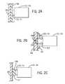
- FIGS. 2A , 2 B, and 2 Cillustrate sectional views of a wall of the casing of FIG. 1 as taken along line 2 - 2 in FIG. 2 , FIGS. 2A , 2 B, and 2 C representing three alternative wall/waveguide configurations.
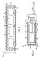
- FIG. 3illustrates a sectional view of a computer CPU casing according to an embodiment.
- FIG. 4illustrates a partial sectional view of a cellular telephone according to an embodiment.
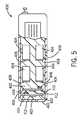
- FIG. 5illustrates a partial sectional view of a cellular telephone according to another embodiment of the present invention.
- FIG. 6illustrates a schematic electrical diagram of an infrared (IR) transceiver for use with the cellular telephone of FIG. 5 .
- IRinfrared
- FIG. 7illustrates a cellular telephone according to another embodiment of the present invention.
- the generic device 100has a casing 102 that defines an interior 104 .
- the casing 102preferably has a metal, plastic, or composite outer portion 106 and a communication bus, such as waveguide portion 108 .
- the casing 102is shown generically as rectangular in shape, however, those skilled in the art will appreciate that it may have any shape.
- the casing 102is shown having a two-piece construction, upper shell 106 a and lower platform 106 b joined together with screws 107 .
- the casing 102can be constructed from one or more pieces, and if more than one piece, the pieces can be joined or fastened in any manner known in the art, such as by welding, gluing, riveting, or with interference or snaps.
- the waveguide portion 108is preferably optical glass having appropriate cladding as is known in the art.
- the waveguide portion 108can also be a synthetic material, such as an acrylic, polycarbonate, or epoxy.
- the inner waveguide materialcan be formed on the casing 102 by any methods known in the art, such as by casting, machining, or depositing.
- the waveguide portion 108can be disposed on the entire inner surface of the outer portion 106 of the casing 102 (or a portion thereof) as shown in FIG. 2A .
- the waveguide portion 108can be arranged in strips 117 , formed on the outer portion 106 of the casing 102 as is shown in FIG.
- the waveguide portion 108can make up the entire shell 102 (no outer portion 106 is used), which can be uncoated or have a coating, such as an opaque paint.
- At least one transmitter 110is arranged on the waveguide portion 108 or proximate thereto such that a signal 101 , such as an optical signal can be transmitted to the waveguide portion 108 .
- the transmitter 110can be integral with a corresponding electronic component 112 or connected thereto.
- detectors 114At another location on the waveguide portion 108 are located detectors 114 for detecting the optical signals in the waveguide portion 108 .
- Each detector 114is either integral with or connected to another electronic/electrical component 116 .
- any componentcan communicate with another component through the waveguide portion 108 , which acts as a communication bus.
- each of the componentscan have both a transmitter 110 and detector 114 such that a two-way communication can be achieved.
- each of the transmitter and detectorcan itself be considered a component operatively connected to the waveguide portion 108 (communication bus).
- mutiplexers and demultiplexerscan be used such that certain components can operate at selected frequencies and/or wavelengths and not interfere with other components on the bus.
- other components known in the art for transmission of signals through a waveguidecan be used, such as an amplifier (not shown) for amplifying a signal between components.
- the transmitters 110 and detectors 114can be mounted to the waveguide portion 108 directly as is known in the art such as by an optical quality adhesive, as shown in FIGS. 2A and 2C .
- the transmitter 110 and detectors 114can be mounted to the waveguide portion 108 or the outer portion 106 of the casing 102 by mechanical means, such as a bracket 113 and screws 115 as is shown in FIG. 2B .
- the transmitters and detectorscan be both adhered and mechanically fastened to the waveguide portion 108 .
- the componentscan be connected to the waveguide portion 108 by optical fibers (not shown) or the like.
- portion 104 a of the interior 104can be used to house additional components or the device can be reduced in size to eliminate portion 104 a or a portion thereof.
- Other advantagesinclude:
- optical transmissionis naturally resistant to very high g-loads and harsh environments
- the systemis inexpensive and extremely low bit rate error (better than 10 ⁇ 12 ) can be readily achieved.
- ultrasoundcan be used to communicate between the internal components 112 , 116 .
- the casing 102 or a portion thereofneeds to be able to carry an ultrasound signal between components.
- Such a casing 102 , or portion thereofmay be constructed from a suitable metal.
- an ultrasonic generatoris used to place signals on the “bus” (casing 102 ) and a corresponding ultrasonic detector detects the ultrasonic signals and relays them to an appropriate component.
- the casingmay also be a synthetic material having portions of suitable materials for carrying an ultrasound signal.
- each componentcan have both an ultrasonic generator and detector such that two-way communication between components is possible and mutiplexers and demultiplexers can be utilized such that certain components can operate at selected frequencies and/or wavelengths and not interfere with other components on the bus.
- the casing 102is a casing of a CPU of a computer 200 .
- the casing 102is a casing of a cellular telephone 300 .
- such embodimentsare given by way of example only and not to limit the scope or spirit of the present invention.
- FIGS. 3 and 4there is shown a computer CPU 200 and cellular telephone 300 , respectively, in which similar number series denote similar features to that of FIG. 1 (i.e., casing 102 corresponds with casings 202 and 302 , etc.).
- casing 102corresponds with casings 202 and 302 , etc.
- the casings 202 , 302can be made smaller than a conventional counterpart device having the same number of internal components or be able to house more components in the same size casing.
- the present inventioncan provide a miniaturization of electronic devices, particularly portable electronic devices while eliminating the problems associated with wiring, such as signal speed, poor connections, and failure over time due to brittleness and other insulation failures.
- the waveguide portion 108also provides for a flexible design and layout of the electronic components as well as the ability to easily add a component on the communication bus (waveguide portion 108 ) of the device. For example, where the waveguide portion 108 is deposited on a substantial portion of the inner surface of the casing 102 , the electronic components can be distributed or added on any portion of the casing where the waveguide portion 108 is deposited.
- Examples of other devices not shown which can benefit from the methods disclosed hereinare PDA's (personal digital assistants), cordless telephones, VCR's, portable CD and MP3 players, digital cameras, DVD players, and televisions. Such a listing is given by way of example only and is not intended to be exhaustive of any other electronic devices.
- PDA'spersonal digital assistants
- cordless telephonesVCR's
- portable CD and MP3 playersdigital cameras
- DVD playersdigital cameras
- televisionstelevisions.
- Such a listingis given by way of example only and is not intended to be exhaustive of any other electronic devices.
- electronic componentscan also have a mechanical or chemical function as well as an electronic/electrical function. These mechanical and/or chemical functions can be housed in a portion of the interior of the casing that has been freed up by having the electronic components distributed on the casing.
- a computer CPU 200having a casing 202 defining an interior 204 .
- the casinghas an outer portion 206 and a waveguide portion 208 that carries a signal 201 .
- Transmitters 210 and detectors 214are operatively connected to the waveguide portion 208 and mounted to respective electronic components 212 , 216 .
- the computer CPU 200can be made smaller, particularly, thinner in height (H) than conventional CPU's that utilize conventional wiring between components.
- the computer CPU 200can house more components than would be possible for a similarly sized CPU of the prior art that utilizes conventional wiring between components.
- the CPU 200has a more versatile design and can be upgraded with additional components at any place on the waveguide portion.
- a cell phone 300having a casing 302 defining an interior 204 .
- the casingalso carries an antenna 305 , a display 303 , and a keyboard and other features (not shown).
- the casing 302has an outer portion 306 and a waveguide portion 308 that carries a signal 301 .
- Transmitters 310 and detectors 314are operatively connected to the waveguide portion 308 and mounted to respective electronic components 312 , 316 .
- the cell phone 300can be miniaturized as compared to conventional cell phones that utilize conventional wiring between components.
- the cell phone 300can house more components than would be possible for a similarly sized cell phones of the prior art that utilizes conventional wiring between components. Additionally, the cell phone 300 is better able to withstand shock, for example from dropping the cell phone 300 on a hard surface. The increased shock resistance is due to the elimination of brittle wiring, including printed circuit boards and wiring harnesses and connecters.
- FIGS. 5 and 6another embodiment of a device is shown, the device being in the form of a cellular telephone and referred to generally by reference numeral 400 .
- electrical/electronic components of some devicessuch as projectiles
- a potting materialsuch as an epoxy
- the potting material 402which can be a solid, such as an epoxy, a gel, or a liquid is disposed within a casing 401 of the cellular telephone and is used as a communication bus between electrical/electronic components 404 .
- the communicationcan be wholly within the potting material 402 or may be partially within the potting material 402 and partially in free space.
- a cellular telephoneis described by way of example because of its tendency to be dropped or otherwise subjected to shock.
- the communication through the potting materialis carried out with a transmitter 406 , which outputs any wavelength radiation that can propagate through the potting material 402 and detected by a receiver 408 .
- the potting material 402be a solid, such as an epoxy to provide hardening of the cellular telephone to shock and noise and it is further preferred that the radiation used as a communication medium is IR energy, preferably from a IR diode.
- the epoxyneed not be transparent or substantially transparent as long as it can carry an IR signal over a required distance, such as several hundred mm or less.
- An example of such an epoxyis Dolphon® CC-1024-A Low Viscosity Potting and Casting Epoxy Resin with RE-2000 Reactor mixed at a ratio of 10 parts resin to 1 part reactor, each of which is distributed by John C. Dolph Company.
- the same epoxy resin and reactorcan be used for the waveguide portions 108 , 208 , or 308 discussed above with regard to FIGS. 1 , 3 , and 4 .
- IR technologyis well known in the art, particularly in the art of remote control of electronic consumer goods.
- the IR data association(IrDA®) has standards for communicating data via short-range infrared transmission. Transmission rates fall within three broad categories SIR, MIR and FIR, SIR (Serial Infrared) speeds cover transmission speeds normally supported by an RS-232 port. MIR (Medium Infrared) usually refers to speeds of 0.576 Mb/s to 1.152 Mb/s.
- FIRFest Infrared denotes transmission speeds of about 4 Mb/s.
- the standardhas been modified for faster transmission speeds up to 16 Mb/s (referred to as very fast Infrared VFIR).
- visible lightfor example from a laser diode, may also be used to transmit communication signals through the potting material 402 .
- the transmitters 406may be carried on printed circuit boards 410 which may also be encased in the potting material 402 or disposed freely throughout the potting material 402 .
- the printed circuit boards each 410preferably carry their own power supply, such as a battery 412 to eliminate internal wiring.
- Each of the electronic/electrical components 404has a receiver 408 for communicating with the transmitters 406 .
- each of the electrical/electronic components 404preferably have a receiver 408 and a transmitter 406 such that they can carry out a two-way communication.
- An example of such a transceiver module 500is shown in the schematic diagram of FIG. 6 .
- FIG. 6shows an (IrDA®) transceiver manufactured by Sharp Inc.
- (2P2W1001YP)which is relatively inexpensive and contains a high speed, high efficiency low power consumption light emitting diode (LD), a silicon PIN photodiode (PD) and a low power bipolar integrated circuit.
- the circuitcontains an LED driver (TRX) and a receiver circuit (RCX) that delivers 4 Mb/s operation for distances of 1 meter.
- the LED emittertransmits at a nominal wavelength of 880nm with a radiant intensity in the range of 100 to 500 mW.sr ⁇ 1 , with a radiation angle of +/ ⁇ 15 degrees.
- the pin photodiodehas an integrated amplifier (AMP) and comparator (CMP), which provide a fixed voltage output over a broad range of input optical power levels and data rates.
- AMPintegrated amplifier
- CMPcomparator
- the Infrared Data Associationwas formed in 1993.
- the Infrared Data Associationspecified wireless communication standard between portable devices, such as, computers, printers, digital cameras, etc., and is preferably used in the present communication links.
- the standardis widely used by the industry.
- IrDA transreceiversbroadcast infrared pulses in a cone that extends 15 degrees half angle to 30 degrees half angle.
- the typical range for IrDA communicationsis from 5 cm to 60 cm away from a transreceiver in the center of the cone. In practice, there are some devices on the market that do not reach one meter, while other devices may reach up to several meters.
- the IrDA standardalso specifies IrLAP (Link Acsess Protocol) and IrLMP (Link Management Protocol).
- the communication protocol schememust tune the transmission rates so that the effects of multi-path effects do not interfere with the operation of the communications links.
- the receiver element located on a separate IR transreceivers at a different location within the projectile bodywill receive the (“leading”) pulse signal, but may also receive several other (“following”) pulses (pulse-like signals) due to the multi-path effects, depending on their relative locations within the projectile body.
- the “following” pulsesare generally weaker and die down quickly after several reflections due to absorption and dispersion. However, up to certain signal strength threshold, the “following” pulses may still register as transmitted signal.
- the next pulsecan only be transmitted once the strength of the aforementioned “following” pulses have fallen below the aforementioned strength threshold.
- the time that it takes for the strength of the “following” pulses to fall below the aforementioned thresholddetermines the maximum transmission rate that can be used in the projectile.
- the said maximum transmission ratecan be readily determined experimentally by transmitting a single pulse and waiting until no pulses above the aforementioned signal strength threshold is detected from any one of the present receivers. This process is preferably implemented on the processor being used to set up the communications bus insider the projectile to allow an appropriate transmission rate to be automatically selected.
- IrDA transreceiversare preferably used in the present munitions and the like applications for setting up a communications bus, however, if a particular application demands, optical transreceivers that operate at different light spectrum may also be employed.
- the casing 402can also be provided with a window portion 403 , as shown in FIG. 5 , which can be used to upload or input data or instructions into components of the cellular telephone through the potting material 402 (or through the waveguide portions 108 , 208 , and 308 discussed above).
- the window portion 403is in optical communication with the waveguide portion 108 , 208 , 308 or potting material 402 and transmits any input signals to the appropriate components on the interior of the cellular telephone.
- the input signalcan be any signal that propagates through the waveguide portion 108 , 208 , 308 or potting material 402 , such as an IR or ultrasound signal.
- the window 403does not have to be a transparent window but merely a portion of the casing, which is capable of transmitting a signal from the exterior of the cellular telephone to one or more components on the interior of the cellular telephone.
- FIG. 7there is shown a cellular telephone according to another embodiment of the present invention, in which similar reference numerals from FIG. 5 denote similar features, the cellular telephone of FIG. 7 being referred to generally by reference numeral 600 .
- FIG. 7is similar to that of FIG. 5 with the exception that the potting material does not have to completely encase a portion of the cellular telephone's interior.
- the interior of the cellular telephoneincludes portions of free space 610 (which may be filled with air or other gases or may be evacuated.
- free space 610which may be filled with air or other gases or may be evacuated.
- all of the components 404 , 408are shown encased in the potting material 402 , they can also be provided in the free space 610 or partially in the free space 610 .
- the communication between componentsis not only through the potting material 402 but can also be done through the free space 610 inside the cellular telephone.
Landscapes
- Physics & Mathematics (AREA)
- Engineering & Computer Science (AREA)
- General Physics & Mathematics (AREA)
- Optics & Photonics (AREA)
- Theoretical Computer Science (AREA)
- Power Engineering (AREA)
- Human Computer Interaction (AREA)
- General Engineering & Computer Science (AREA)
- Signal Processing (AREA)
- Computer Hardware Design (AREA)
- Electromagnetism (AREA)
- Computer Networks & Wireless Communication (AREA)
- Optical Communication System (AREA)
Abstract
Description
Claims (6)
Priority Applications (1)
| Application Number | Priority Date | Filing Date | Title |
|---|---|---|---|
| US12/889,391US8414198B2 (en) | 2003-08-12 | 2010-09-23 | Device having a casing and/or interior acting as a communication bus between electronic components |
Applications Claiming Priority (3)
| Application Number | Priority Date | Filing Date | Title |
|---|---|---|---|
| US10/639,001US7272293B2 (en) | 2003-08-12 | 2003-08-12 | Device having a casing and /or interior acting as a communication bus between electronic components |
| US11/899,731US20080253774A1 (en) | 2003-08-12 | 2007-09-07 | Device having a casing containing a potting material for transmitting signals between electronic components |
| US12/889,391US8414198B2 (en) | 2003-08-12 | 2010-09-23 | Device having a casing and/or interior acting as a communication bus between electronic components |
Related Parent Applications (2)
| Application Number | Title | Priority Date | Filing Date |
|---|---|---|---|
| US11/899,731Continuation-In-PartUS20080253774A1 (en) | 2003-08-12 | 2007-09-07 | Device having a casing containing a potting material for transmitting signals between electronic components |
| US11/899,779Continuation-In-PartUS20080002342A1 (en) | 2003-08-12 | 2007-09-07 | Computer having a casing and/or interior acting as a communication bus between electronic components |
Publications (2)
| Publication Number | Publication Date |
|---|---|
| US20110076029A1 US20110076029A1 (en) | 2011-03-31 |
| US8414198B2true US8414198B2 (en) | 2013-04-09 |
Family
ID=43780524
Family Applications (1)
| Application Number | Title | Priority Date | Filing Date |
|---|---|---|---|
| US12/889,391Expired - Fee RelatedUS8414198B2 (en) | 2003-08-12 | 2010-09-23 | Device having a casing and/or interior acting as a communication bus between electronic components |
Country Status (1)
| Country | Link |
|---|---|
| US (1) | US8414198B2 (en) |
Families Citing this family (4)
| Publication number | Priority date | Publication date | Assignee | Title |
|---|---|---|---|---|
| US8160407B2 (en)* | 2003-08-12 | 2012-04-17 | Omnitek Partners Llc | Computer having a casing and/or interior acting as a communication bus between electronic components |
| US8414198B2 (en)* | 2003-08-12 | 2013-04-09 | Omnitek Partners Llc | Device having a casing and/or interior acting as a communication bus between electronic components |
| US8547036B2 (en)* | 2011-11-20 | 2013-10-01 | Available For Licensing | Solid state light system with broadband optical communication capability |
| WO2019046047A1 (en)* | 2017-09-01 | 2019-03-07 | Commscope Technologies Llc | Systems and methods for wireless communication within a base station antenna structure |
Citations (27)
| Publication number | Priority date | Publication date | Assignee | Title |
|---|---|---|---|---|
| US3623045A (en)* | 1970-11-23 | 1971-11-23 | Us Army | Internal gun tube ballistics laser telemeter |
| US3717413A (en)* | 1969-11-20 | 1973-02-20 | Tokyo Shibaura Electric Co | Sun sensing system for a flying body |
| US3780966A (en)* | 1972-09-14 | 1973-12-25 | Nasa | Attitude sensor |
| US6260792B1 (en)* | 1981-05-04 | 2001-07-17 | Raytheon Company | Tracking and guidance system with modulated missile-mounted laser beacon |
| US6308912B1 (en)* | 1997-10-21 | 2001-10-30 | Natural Colour Kari Kirjavainen Oy | Rotorcraft |
| US6398155B1 (en)* | 2001-01-02 | 2002-06-04 | The United States Of America As Represented By The Secretary Of The Army | Method and system for determining the pointing direction of a body in flight |
| US20030044665A1 (en)* | 2001-09-05 | 2003-03-06 | Rastegar Jahangir S. | Conformal power supplies |
| US6530539B2 (en)* | 2001-02-09 | 2003-03-11 | Raytheon Company | Internal fluid cooled window assembly |
| US20040066095A1 (en)* | 2002-10-02 | 2004-04-08 | Hewlett-Packard Company | Apparatus for controlling transmissions to reduce electromagnetic interference in an electronic system |
| US6733189B2 (en)* | 2000-02-02 | 2004-05-11 | Infineon Technologies Ag | Electrooptical transmitting/receiving module, and method for producing the module |
| US6795174B1 (en)* | 1992-10-24 | 2004-09-21 | Mbda Uk Limited | Tracking systems |
| US20050036273A1 (en)* | 2003-08-12 | 2005-02-17 | Rastegar Jahangir S. | Device having a casing and /or interior acting as a communication bus between electronic components |
| US20050039625A1 (en)* | 2003-08-12 | 2005-02-24 | Rastegar Jahangir S. | Projectile having a casing and/or interior acting as a communication bus between electronic components |
| US6946642B2 (en)* | 2000-10-26 | 2005-09-20 | Rafael-Armament Development Authority Ltd. | Optical window assembly for use in a supersonic platform |
| US6955324B2 (en)* | 2003-10-22 | 2005-10-18 | The Boeing Company | Laser-tethered vehicle |
| US20050277826A1 (en)* | 2004-06-10 | 2005-12-15 | Conopco, Inc. | Apparatus and method for reducing interference |
| US7079944B2 (en)* | 2003-08-18 | 2006-07-18 | Textron Systems Corporation | System and method for determining orientation based on solar positioning |
| US7145734B2 (en)* | 2004-08-03 | 2006-12-05 | Raytheon Company | Windowed optical system having a tilted optical element to correct aberrations |
| US20080025235A1 (en)* | 1993-08-03 | 2008-01-31 | Mahany Ronald L | System and method for controlling communication in a multi-network environment |
| US7421321B2 (en)* | 1995-06-07 | 2008-09-02 | Automotive Technologies International, Inc. | System for obtaining vehicular information |
| US7444210B2 (en)* | 2000-09-08 | 2008-10-28 | Automotive Technologies International, Inc. | System and method for in-vehicle communications |
| US20090256024A1 (en)* | 2003-08-12 | 2009-10-15 | Omnitek Partners Llc | Projectile Having A Window For Transmitting Power and/or Data Into The Projectile Interior |
| US20100239255A1 (en)* | 2009-03-18 | 2010-09-23 | Hiroki Ikeda | Optical line terminal, passive optical network system, and bandwidth assignment method |
| US20110076030A1 (en)* | 2003-08-12 | 2011-03-31 | Omnitek Partners Llc | Computer Having a Casing and/or Interior Acting as a Communication Bus Between Electronic Components |
| US20110076029A1 (en)* | 2003-08-12 | 2011-03-31 | Omnitek Partners Llc | Device Having a Casing and/or Interior Acting as a Communication Bus Between Electronic Components |
| US8014681B1 (en)* | 2007-11-27 | 2011-09-06 | National Semiconductor Corporation | Device with optically transparent housing for conducting light signals and methods of manufacture and use |
| US8110784B2 (en)* | 2003-08-12 | 2012-02-07 | Omnitek Partners Llc | Projectile having one or more windows for transmitting power and/or data into/from the projectile interior |
- 2010
- 2010-09-23USUS12/889,391patent/US8414198B2/ennot_activeExpired - Fee Related
Patent Citations (33)
| Publication number | Priority date | Publication date | Assignee | Title |
|---|---|---|---|---|
| US3717413A (en)* | 1969-11-20 | 1973-02-20 | Tokyo Shibaura Electric Co | Sun sensing system for a flying body |
| US3623045A (en)* | 1970-11-23 | 1971-11-23 | Us Army | Internal gun tube ballistics laser telemeter |
| US3780966A (en)* | 1972-09-14 | 1973-12-25 | Nasa | Attitude sensor |
| US6260792B1 (en)* | 1981-05-04 | 2001-07-17 | Raytheon Company | Tracking and guidance system with modulated missile-mounted laser beacon |
| US6795174B1 (en)* | 1992-10-24 | 2004-09-21 | Mbda Uk Limited | Tracking systems |
| US20080025235A1 (en)* | 1993-08-03 | 2008-01-31 | Mahany Ronald L | System and method for controlling communication in a multi-network environment |
| US7421321B2 (en)* | 1995-06-07 | 2008-09-02 | Automotive Technologies International, Inc. | System for obtaining vehicular information |
| US6308912B1 (en)* | 1997-10-21 | 2001-10-30 | Natural Colour Kari Kirjavainen Oy | Rotorcraft |
| US6733189B2 (en)* | 2000-02-02 | 2004-05-11 | Infineon Technologies Ag | Electrooptical transmitting/receiving module, and method for producing the module |
| US7444210B2 (en)* | 2000-09-08 | 2008-10-28 | Automotive Technologies International, Inc. | System and method for in-vehicle communications |
| US6946642B2 (en)* | 2000-10-26 | 2005-09-20 | Rafael-Armament Development Authority Ltd. | Optical window assembly for use in a supersonic platform |
| US6398155B1 (en)* | 2001-01-02 | 2002-06-04 | The United States Of America As Represented By The Secretary Of The Army | Method and system for determining the pointing direction of a body in flight |
| US6530539B2 (en)* | 2001-02-09 | 2003-03-11 | Raytheon Company | Internal fluid cooled window assembly |
| US20030044665A1 (en)* | 2001-09-05 | 2003-03-06 | Rastegar Jahangir S. | Conformal power supplies |
| US20040066095A1 (en)* | 2002-10-02 | 2004-04-08 | Hewlett-Packard Company | Apparatus for controlling transmissions to reduce electromagnetic interference in an electronic system |
| US20080253774A1 (en)* | 2003-08-12 | 2008-10-16 | Rastegar Jahangir S | Device having a casing containing a potting material for transmitting signals between electronic components |
| US20050039625A1 (en)* | 2003-08-12 | 2005-02-24 | Rastegar Jahangir S. | Projectile having a casing and/or interior acting as a communication bus between electronic components |
| US8160407B2 (en)* | 2003-08-12 | 2012-04-17 | Omnitek Partners Llc | Computer having a casing and/or interior acting as a communication bus between electronic components |
| US8110784B2 (en)* | 2003-08-12 | 2012-02-07 | Omnitek Partners Llc | Projectile having one or more windows for transmitting power and/or data into/from the projectile interior |
| US7272293B2 (en)* | 2003-08-12 | 2007-09-18 | Omnitek Partners Llc | Device having a casing and /or interior acting as a communication bus between electronic components |
| US20080002342A1 (en)* | 2003-08-12 | 2008-01-03 | Rastegar Jahangir S | Computer having a casing and/or interior acting as a communication bus between electronic components |
| US20080004086A1 (en)* | 2003-08-12 | 2008-01-03 | Rastegar Jahangir S | Device having a casing and/or interior acting as a communication bus between electronic components |
| US20110076029A1 (en)* | 2003-08-12 | 2011-03-31 | Omnitek Partners Llc | Device Having a Casing and/or Interior Acting as a Communication Bus Between Electronic Components |
| US6892644B2 (en)* | 2003-08-12 | 2005-05-17 | Omnitek Partners Llc | Projectile having a casing and/or interior acting as a communication bus between electronic components |
| US20110076030A1 (en)* | 2003-08-12 | 2011-03-31 | Omnitek Partners Llc | Computer Having a Casing and/or Interior Acting as a Communication Bus Between Electronic Components |
| US20050036273A1 (en)* | 2003-08-12 | 2005-02-17 | Rastegar Jahangir S. | Device having a casing and /or interior acting as a communication bus between electronic components |
| US20090256024A1 (en)* | 2003-08-12 | 2009-10-15 | Omnitek Partners Llc | Projectile Having A Window For Transmitting Power and/or Data Into The Projectile Interior |
| US7079944B2 (en)* | 2003-08-18 | 2006-07-18 | Textron Systems Corporation | System and method for determining orientation based on solar positioning |
| US6955324B2 (en)* | 2003-10-22 | 2005-10-18 | The Boeing Company | Laser-tethered vehicle |
| US20050277826A1 (en)* | 2004-06-10 | 2005-12-15 | Conopco, Inc. | Apparatus and method for reducing interference |
| US7145734B2 (en)* | 2004-08-03 | 2006-12-05 | Raytheon Company | Windowed optical system having a tilted optical element to correct aberrations |
| US8014681B1 (en)* | 2007-11-27 | 2011-09-06 | National Semiconductor Corporation | Device with optically transparent housing for conducting light signals and methods of manufacture and use |
| US20100239255A1 (en)* | 2009-03-18 | 2010-09-23 | Hiroki Ikeda | Optical line terminal, passive optical network system, and bandwidth assignment method |
Also Published As
| Publication number | Publication date |
|---|---|
| US20110076029A1 (en) | 2011-03-31 |
Similar Documents
| Publication | Publication Date | Title |
|---|---|---|
| US20080253774A1 (en) | Device having a casing containing a potting material for transmitting signals between electronic components | |
| US8414198B2 (en) | Device having a casing and/or interior acting as a communication bus between electronic components | |
| US9423227B2 (en) | Method for optically transmitting data into and from a casing of a projectile | |
| US9118420B2 (en) | Method and apparatus for optical communication using a retro-reflector | |
| CN203587801U (en) | Proximity and light sensing device | |
| US6256296B1 (en) | Network communications link | |
| US8467689B2 (en) | Parallel-serial converter for optical transmission, optical transmission system, and electronic apparatus | |
| US20090256024A1 (en) | Projectile Having A Window For Transmitting Power and/or Data Into The Projectile Interior | |
| US8588558B2 (en) | Optical link circuit and method of making same | |
| CN102193154A (en) | Optical transmission module, electronic device, and method for manufacturing optical transmission module | |
| CN101741935B (en) | Light transmitting system and electronic device having the same | |
| US8160407B2 (en) | Computer having a casing and/or interior acting as a communication bus between electronic components | |
| WO2020029739A1 (en) | Optical module | |
| US6892644B2 (en) | Projectile having a casing and/or interior acting as a communication bus between electronic components | |
| CN112564791A (en) | Wireless optical transmission module and assembly thereof | |
| CN209433063U (en) | Multichannel wavelength division multiplexed light receiving unit and optical module | |
| CN212083742U (en) | Optical module | |
| US20190391331A1 (en) | Optical module | |
| US6574020B1 (en) | System and method for optically and mechanically coupling an avionics line replaceable unit with other equipment on an aircraft | |
| US8014681B1 (en) | Device with optically transparent housing for conducting light signals and methods of manufacture and use | |
| US20090154934A1 (en) | Optical Transceiver Method and Apparatus | |
| CN208780855U (en) | A kind of transmitting-receiving subassembly of wavelength-division multiplex transceiver module | |
| CN201167325Y (en) | Infrared communication device capable of framing locating using camera | |
| KR20090121334A (en) | Optical transmission system and electronic device | |
| WO1999056417A2 (en) | A device and method for wireless data transmission |
Legal Events
| Date | Code | Title | Description |
|---|---|---|---|
| AS | Assignment | Owner name:OMNITEK PARTNERS LLC, NEW YORK Free format text:ASSIGNMENT OF ASSIGNORS INTEREST;ASSIGNORS:RASTEGAR, JAHANGIR S.;SPINELLI, THOMAS;REEL/FRAME:025496/0819 Effective date:20101122 | |
| AS | Assignment | Owner name:OMNITEK PARTNERS LLC, NEW YORK Free format text:CHANGE OF ASSIGNEE ADDRESS;ASSIGNOR:OMNITEK PARTNERS LLC;REEL/FRAME:028583/0175 Effective date:20111101 | |
| STCF | Information on status: patent grant | Free format text:PATENTED CASE | |
| REMI | Maintenance fee reminder mailed | ||
| FPAY | Fee payment | Year of fee payment:4 | |
| SULP | Surcharge for late payment | ||
| FEPP | Fee payment procedure | Free format text:MAINTENANCE FEE REMINDER MAILED (ORIGINAL EVENT CODE: REM.); ENTITY STATUS OF PATENT OWNER: SMALL ENTITY | |
| FEPP | Fee payment procedure | Free format text:7.5 YR SURCHARGE - LATE PMT W/IN 6 MO, SMALL ENTITY (ORIGINAL EVENT CODE: M2555); ENTITY STATUS OF PATENT OWNER: SMALL ENTITY | |
| MAFP | Maintenance fee payment | Free format text:PAYMENT OF MAINTENANCE FEE, 8TH YR, SMALL ENTITY (ORIGINAL EVENT CODE: M2552); ENTITY STATUS OF PATENT OWNER: SMALL ENTITY Year of fee payment:8 | |
| FEPP | Fee payment procedure | Free format text:MAINTENANCE FEE REMINDER MAILED (ORIGINAL EVENT CODE: REM.); ENTITY STATUS OF PATENT OWNER: SMALL ENTITY | |
| LAPS | Lapse for failure to pay maintenance fees | Free format text:PATENT EXPIRED FOR FAILURE TO PAY MAINTENANCE FEES (ORIGINAL EVENT CODE: EXP.); ENTITY STATUS OF PATENT OWNER: SMALL ENTITY | |
| STCH | Information on status: patent discontinuation | Free format text:PATENT EXPIRED DUE TO NONPAYMENT OF MAINTENANCE FEES UNDER 37 CFR 1.362 | |
| FP | Lapsed due to failure to pay maintenance fee | Effective date:20250409 |