US8411790B2 - Power line communications apparatus - Google Patents
Power line communications apparatusDownload PDFInfo
- Publication number
- US8411790B2 US8411790B2US13/336,569US201113336569AUS8411790B2US 8411790 B2US8411790 B2US 8411790B2US 201113336569 AUS201113336569 AUS 201113336569AUS 8411790 B2US8411790 B2US 8411790B2
- Authority
- US
- United States
- Prior art keywords
- capacitor
- terminal
- coupled
- digital
- power line
- Prior art date
- Legal status (The legal status is an assumption and is not a legal conclusion. Google has not performed a legal analysis and makes no representation as to the accuracy of the status listed.)
- Active
Links
Images


Classifications
- H—ELECTRICITY
- H04—ELECTRIC COMMUNICATION TECHNIQUE
- H04B—TRANSMISSION
- H04B3/00—Line transmission systems
- H04B3/54—Systems for transmission via power distribution lines
- H—ELECTRICITY
- H04—ELECTRIC COMMUNICATION TECHNIQUE
- H04B—TRANSMISSION
- H04B14/00—Transmission systems not characterised by the medium used for transmission
- H04B14/02—Transmission systems not characterised by the medium used for transmission characterised by the use of pulse modulation
- H04B14/026—Transmission systems not characterised by the medium used for transmission characterised by the use of pulse modulation using pulse time characteristics modulation, e.g. width, position, interval
- H—ELECTRICITY
- H04—ELECTRIC COMMUNICATION TECHNIQUE
- H04B—TRANSMISSION
- H04B3/00—Line transmission systems
- H04B3/54—Systems for transmission via power distribution lines
- H04B3/56—Circuits for coupling, blocking, or by-passing of signals
- H—ELECTRICITY
- H04—ELECTRIC COMMUNICATION TECHNIQUE
- H04B—TRANSMISSION
- H04B2203/00—Indexing scheme relating to line transmission systems
- H04B2203/54—Aspects of powerline communications not already covered by H04B3/54 and its subgroups
- H04B2203/5404—Methods of transmitting or receiving signals via power distribution lines
- H04B2203/5416—Methods of transmitting or receiving signals via power distribution lines by adding signals to the wave form of the power source
Definitions
- Embodiments of the present disclosurerelate generally to power line communications and, more particularly, to an apparatus for providing communication over power lines.
- PLCPower Line Communications
- PLCis a technology for utilizing power lines, such as the existing commercial AC power grid infrastructure, to communicate data between devices coupled to the power lines.
- PLCtypically operates in a point-to-multipoint fashion where one transmitter at a time transmits over the power line while other devices coupled to the power line receive the transmitted signal.
- a transmitterFor PLC transmission, a transmitter is generally coupled to the power line through an isolation transformer and sends a voltage stimulus on the power line (i.e., a voltage-based signal) in accordance with relevant standards for PLC, such as BS EN 50065-1:2001 “Specification for Signaling on Low-Voltage Electrical Installations in the Frequency Range 3 kHz to 148.5 kHz”. These relevant standards set forth specifications for PLC operation, such as a maximum voltage level. As a result of power lines having undefined and variable impedances within the frequency band of interest for PLC, a transmitter module may be required to generate a large amount of current, for example on the order of hundreds of milliamperes, in order to meet the PLC voltage requirements.
- PLC transmittersuse linear amplifiers to achieve the required amplification and signal processing for PLC transmission.
- such devicesdissipate high levels of power when operating to drive large currents on the power line and thus decrease the efficiency of the PLC transmitters.
- the PLC transmittersgenerally perform filtering prior to the power amplification in order to satisfy spectral purity requirements set forth in the relevant standards, requiring a large number of costly components.
- a PLC receiverFor receiving data transmitted over the power line, a PLC receiver is typically also coupled to the power line through an isolation transformer.
- the PLC receiveris required to provide a large input impedance to limit noise from the power line into the receiver prior to amplification, thereby requiring a costly number of components to perform such functions.
- Embodiments of the present inventiongenerally relate to an apparatus and system for communicating data via a power line.
- the apparatuscomprises a transmitter comprising a modulator for generating a second digital signal based on input data; a digital buffer for amplifying the second digital signal to generate a third digital signal; a filter for filtering the third digital signal to generate an analog output waveform; and a coupler for coupling the analog output waveform to the power line.
- FIG. 1is a block diagram of a system for communicating data over an AC power line in accordance with one or more embodiments of the present invention
- FIG. 2is a block diagram of a transmitter in accordance with one or more embodiments of the present invention.
- FIG. 3is a block diagram of a receiver in accordance with one or more embodiments of the present invention.
- FIG. 4is a block diagram of a coupler in accordance with one or more embodiments of the present invention.
- FIG. 5is a block diagram of a system for inverting solar generated DC power to AC power using one or more embodiments of the present invention.
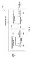
- FIG. 1is a block diagram of a system 100 for communicating data over an AC power line in accordance with one or more embodiments of the present invention.
- the system 100comprises a device 102 coupled to a power line communications transceiver (PLCT) 104 , which is further coupled to an AC power line 120 (“power line 120 ”) via a junction box 114 .
- PLCTpower line communications transceiver
- the system 100comprises a device 102 A coupled to a PLCT 104 A, which is further coupled to the power line 120 via a junction box 114 A.
- the devices 102 and 102 Aare devices requiring communications bandwidth for transmitting and/or receiving data, such as a home computer, peripheral device, and the like, and are capable of communicating with one another over the power line 120 via the PLCTs 104 and 104 A, respectively.
- the PLCT 104 and/or the PLCT 104 Amay be coupled directly to the power line 120 without the use of junction boxes 114 / 114 A.
- junction boxes 114 / 114 AOne particular embodiment that uses the inventive system is described below with respect to FIG. 5 .
- the PLCT 104comprises a transmitter 106 and a receiver 108 , each coupled to the device 102 , and a coupler 110 that couples both the transmitter 106 and the receiver 108 to the junction box 114 .
- the transmitter 106is capable of transmitting data to the device 102 A via the power line 120 .
- the receiver 108is capable of receiving data from the device 102 A via the power line 120 .
- the PLCT 104may be able to simultaneously receive and transmit data; however, the transmitter 106 may generally blind the receiver 108 while active.
- a controller 116is coupled to the transmitter 106 and provides a control signal for enabling and disabling the transmit mode.
- the controller 116may be separate from the PLCT 104 as depicted in FIG. 1 , or, alternatively, the controller 116 may be a component of the PLCT 104 .
- the PLCT 104 Acomprises a transmitter 106 A, a receiver 108 A, and a coupler 110 A.
- the transmitter 106 A and receiver 108 Aare coupled to the device 102 A as well as the coupler 110 A, and the coupler 110 A is further coupled to the junction box 114 A.
- the transmitter 106 Ais capable of transmitting data to the device 102 via the power line 120 .
- the receiver 108 Ais capable of receiving data from the device 102 via the power line 120 .
- the PLCT 104 Amay be able to simultaneously receive and transmit data; however, the transmitter 106 A may generally blind the receiver 108 A while active.
- a controller 116 Ais coupled to the transmitter 106 A and provides a control signal for enabling and disabling the transmit mode.
- the controller 116 Amay be separate from the PLCT 104 A as depicted in FIG. 1 , or, alternatively, the controller 116 A may be a component of the PLCT 104 A.
- the transmitter 106when operating in the transmit mode the transmitter 106 receives digital input data from the device 102 and digitally processes the received data through a voltage amplification stage to generate digitally processed data. Following the voltage amplification stage, the transmitter 106 generates an analog voltage waveform for transmitting the digitally processed data over the power line 120 such that the analog voltage waveform characteristics (e.g., frequency, magnitude, spectral purity, and the like) meet relevant standards for PLC.
- analog voltage waveform characteristicse.g., frequency, magnitude, spectral purity, and the like
- the analog voltage waveformmay be generated to have a frequency within the band 50-500 KHz (for example, in the 95-148 KHz band) and a maximum voltage on the order of 1 volt root mean square (RMS), i.e., 120 decibel/microvolt (dB ⁇ V).
- RMSroot mean square
- the coupler 110couples the generated analog voltage waveform to the power line 120 .
- the transmitter 106During the transmit mode, the transmitter 106 presents a minimal impedance (e.g., within a range of 1-5 ohms) to the power line 120 .
- the transmitter 106In order to meet required output voltage levels given the variability of impedance on the power line 120 , the transmitter 106 is capable of driving large currents, for example on the order of hundreds of milliamperes, on the power line 120 .
- the transmitter 106may employ a high-current rated complementary metal-oxide-semiconductor (CMOS) buffer, as described further below, for performing the voltage amplification in the digital domain and driving the necessary current levels.
- CMOScomplementary metal-oxide-semiconductor
- the coupler 110couples an analog signal from the power line 120 to the receiver 108 .
- the receiver 108converts the received analog voltage waveform to digital output data and provides the digital output data to the device 102 .
- the digital output datamay be a digital representation of a modulated signal; for example, the digital output data may be a digital representation of an FSK signal (a digital FSK signal), and an FSK demodulator is contained within the device 102 or coupled between the receiver 108 and the device 102 .
- the receiver 108may comprise a band-pass filter for filtering the received waveform to remove noise inherent to the power line 120 .
- the PLCT 104When the transmit mode is disabled, the PLCT 104 presents a large input impedance to the power line 120 (e.g., on the order of kilo-ohms). Such a large input impedance prevents the transmitter 106 from being “swamped out” when a large number of nodes are present on the power line 120 .
- the PLCT 104comprises only the transmitter 106 and the coupler 110 for transmitting information via the power line 120 ; additionally or alternatively, the PLCT 104 A may comprise only the transmitter 106 A and the coupler 110 A for transmitting information via the power line 120 .
- the receivers 108 and/or 108 Aare not used. The optional nature of including a receiver is represented by the dashed boxes of receivers 108 and 108 A.
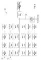
- FIG. 2is a block diagram of a transmitter 106 in accordance with one or more embodiments of the present invention.
- the transmitter 106comprises a frequency control generator 202 coupled to a direct digital synthesizer (DDS) 204 , which is further coupled to a delta-sigma ( ⁇ ) modulator 206 .
- the ⁇ modulator 206is coupled to a CMOS buffer 208 , and an output from the CMOS buffer 208 is coupled to a low-pass filter 210 .
- the CMOS buffer 208is additionally coupled to the controller 116 for receiving an input to enable/disable the transmit mode.
- the CMOS buffer 208When the transmit mode is enabled, the CMOS buffer 208 presents a low transmit impedance (e.g., on the order of 1-5 ohms); when the transmit mode is disabled, the CMOS buffer 208 present a large input impedance (e.g., on the order of kilo-ohms).
- the frequency control generator 202is coupled to the device 102 for receiving a digital input data signal for transmission over the power line 120 .
- the frequency control generator 202generates a digital frequency control signal (for example, a 16 to 24 bit signal) based on the received data signal and couples the digital frequency control signal to the DDS 204 .
- the DDS 204operates at a high frequency and, in accordance with the frequency control signal, generates a digital frequency-shift keying (FSK) signal (i.e., a digital representation of an FSK signal).
- the digital FSK signalmay be on the order of 8-10 bits wide at a frequency of 25 MHz; alternatively, the digital FSK signal may comprise fewer or more bits and/or may be at a different frequency.
- minimum FSK modulationmay be utilized; in some other alternative embodiments, modulation techniques other than FSK modulation may be utilized, such as M-ary quadrature amplitude modulation (QAM), quadrature phase-shift keying (QPSK), phase-shift keying (PSK), orthogonal frequency-division multiplexing (OFDM), pulse-amplitude modulation (PAM), or the like.
- QAMquadrature amplitude modulation
- QPSKquadrature phase-shift keying
- PSKphase-shift keying
- OFDMorthogonal frequency-division multiplexing
- PAMpulse-amplitude modulation
- the DDS 204 output signalis coupled to the ⁇ modulator 206 , which may be a single-stage ⁇ modulator or a multi-stage ⁇ modulator.
- the ⁇ modulator 206encodes the received digital FSK signal utilizing pulse-density modulation (PDM) and provides a digital 1-bit output signal representing the received digital FSK signal.
- PDMpulse-density modulation
- the ⁇ modulator 206may operate at a frequency of 25 MHz; in alternative embodiments, the ⁇ modulator 206 may operate at a different frequency.
- the frequency control generator 202 , DD 2 204 , and ⁇ modulator 206form a modulator 212 that generates a digital signal based on the digital input data signal from the device 102 .
- the digital signal from the modulator 212i.e., the output of the ⁇ modulator 206
- the CMOS buffer 208may be a high-current rated CMOS buffer capable of providing sufficient current (e.g., hundreds of milliamperes) to maintain a required output voltage level when the power line impedance is very low; in some embodiments, the CMOS buffer 208 may be on the order of 0.15 to 0.25 micron technology.
- the CMOS buffer 208may comprise a plurality of buffers (e.g., sixteen buffers) coupled in parallel, each buffer capable of producing current on the order of 50 mA.
- the number of buffers coupled in paralleldetermines the amount of current that can be driven and is considered a design choice for the system.
- the CMOS buffer 208produces a digital output signal which is coupled to the low-pass filter 210 and filtered to generate an analog output.
- the low-pass filteringcan be performed in the MHz frequency band to remove sufficient artifacts resulting from the ⁇ modulation.
- the output of the low-pass filter 210is coupled to the power line 120 through the coupler 110 , as explained further below with respect to FIG. 4 .
- FIG. 3is a block diagram of a receiver 108 in accordance with one or more embodiments of the present invention.
- the receiver 108receives an analog voltage waveform from the power line 120 through the coupler 110 , as further described below, and generates a digital output data signal that is coupled to the device 102 .
- the receiver 108comprises capacitors 302 , 304 , 306 , and 314 ; an inductor 308 ; resistors 312 and 310 ; and an analog-to-digital (A/D) converter 316 .
- one or more the capacitors/inductor/resistorsmay be a parasitic component.
- the capacitors 302 , 304 , and 306are coupled in series such that the capacitor 302 is coupled to the capacitor 304 which is in turn coupled to the capacitor 306 , and the received analog waveform is coupled from the coupler 110 across the series combination of capacitors 302 , 304 , and 306 .
- the inductor 308is coupled across the series combination of the capacitors 304 and 306 .
- the capacitors 302 , 304 , and 306 and the inductor 308perform band-pass filtering of the received analog voltage waveform to reduce noise that is inherently present on the power line 120 (i.e., to pass the signal of interest with minimal phase/amplitude distortion).
- the resistor 310is coupled across the capacitor 306 .
- the resistor 312is coupled between a first terminal of the resistor 310 and a first terminal of the capacitor 314 ; a second terminal of the resistor 310 is coupled to a second terminal of the capacitor 314 .
- the A/D converter 316is coupled across the capacitor 314 and is further coupled to the device 102 .
- the resistors 310 and 312form a high impedance resistive load, and the A/D converter 316 samples the voltage across this load to produce an FSK-modulated digital output signal for the device 102 (i.e., a digital representation of an FSK signal).
- the device 102comprises an FSK demodulator for demodulating the digital output signal; alternatively, an FSK demodulator may be coupled between the receiver 108 and the device 102 .
- the digital output data signalmay be a digital representation of a minimum FSK modulated signal, a QAM modulated signal, a QPSK modulated signal, a PSK modulated signal, an OFDM modulated signal, a PAM modulated signal, or the like.
- the resistors 310 and 312may each be on the order of a few hundred ohms; the capacitors 304 , 306 , and 314 may each be on the order of a few nanofarads; the capacitor 302 may be on the order of several hundred picofarads; and the inductor 308 may be on the order of a few hundred microhenries.
- FIG. 4is a block diagram of a coupler 110 in accordance with one or more embodiments of the present invention.
- the coupler 110comprises a transformer 402 , an inductor 404 to represent a leakage inductance of the transformer 402 , a resistor 406 , and capacitors 408 and 410 .
- the coupler 110may be simplified.
- the transmit signalmust be low pass filtered without increasing the output impedance and loading the receiver while inactive; the receive signal must be band pass filtered to pass the signal of interest and attenuate out of band noise, while maintaining high impedance in the band of interest.
- the transformer 402is an isolation transformer having a high coupling factor; for example, the coupling factor may be 0.95 or greater. Generally, the transformer 402 has a 1:1 turns ratio, although other turns ratios may also be utilized.
- a primary winding of the transformer 402is coupled across each of the transmitter 106 and the receiver 108 .
- a first terminal of a secondary winding of the transformer 402is depicted as coupled to a first terminal of the inductor 404 .
- the resistor 406is coupled between a second terminal of the inductor 404 and a first terminal of the capacitor 408 , which provides a safety function for coupling to the power line 120 .
- the resistor 406acts to damp an RLC tank formed by the resistor 406 , the inductor 404 , and the capacitor 408 .
- the capacitor 410is coupled between a second terminal of the capacitor 408 and a second terminal of the secondary winding of the transformer 402 , and is further coupled across two output terminals of the coupler 110 for coupling to the power line 120 through the junction box 114 .
- the capacitor 410provides an optional low-pass filtering function; in some alternative embodiments, the capacitor 410 may be removed from the coupler 110 .
- the coupler 110couples the outbound analog voltage waveform from the transmitter 106 to the power line 120 and couples the inbound analog voltage waveform from the power line 120 to the receiver 108 .
- the primary and secondary windings of the transformer 402each have an inductance on the order of a few hundred microhenries; the inductor 404 (i.e., the leakage inductance of the transformer 402 ) is on the order of a few microhenries; the resistor 406 is on the order of a few ohms; the capacitor 408 is on the order of a few hundred nanofarads; and the capacitor 410 is on the order of a few nanofarads.
- FIG. 5is a block diagram of a system 500 for inverting solar generated DC power to AC power using one or more embodiments of the present invention. This diagram only portrays one variation of the myriad of possible system configurations and devices that may utilize the present invention.
- the present inventioncan be utilized by any device for power line communication, and can function in a variety of distributed environments and systems requiring communications over power lines.
- the system 500comprises a plurality of inverters 502 1 , 502 2 . . . 502 n , collectively referred to as inverters 502 , a plurality of PV modules 504 1 , 504 2 . . . 504 n , collectively referred to as PV modules 504 , a plurality of PLCTs 512 1 , 512 2 . . . 512 n , 512 n+1 , collectively referred to as PLCTs 512 , AC power line 506 , an inverter controller 510 , and a load center 508 .
- Each inverter 502 1 , 502 2 . . . 502 nis coupled to a PLCT 512 1 , 512 2 . . . 512 n , respectively; in some alternative embodiments, each of the PLCTs 512 1 , 512 2 . . . 512 n may be contained within the corresponding inverter 502 1 , 502 2 . . . 502 n .
- Each inverter 502 1 , 502 2 . . . 502 nis additionally coupled to a PV module 504 1 , 504 2 . . . 504 n , respectively.
- the inverter controller 510is coupled to the PLCT 512 n+1 .
- the PLCTs 512are coupled to the AC power line 506 and operate analogously to the PLCTs 104 and 104 A described above.
- each of the PLCTs 512may be coupled to a controller (i.e., one controller per PLCT 512 ), such as controller 116 , for enabling/disabling a transmit mode of the PLCT 512 .
- the AC power line 506is further coupled to the load center 508 which houses connections between incoming commercial AC power lines from a commercial AC power grid distribution system and the AC power line 506 .
- the inverters 502convert DC power generated by the PV modules 504 into AC power, and meter out AC current that is in-phase with the commercial AC power grid voltage.
- the system 500couples the generated AC power to the commercial AC power grid via the load center 508 .
- the inverter controller 510is capable of receiving data from the inverters 502 and issuing command and control signals to the inverters 502 for controlling the functionality of the inverters 502 .
- the PLCTs 512enable such communication between the inverters 502 and the inverter controller 510 over the AC power lines 506 .
- the PLCTs 512digitally process digital input data from the inverters 502 and/or the inverter controller 510 through a voltage amplification stage and generate a corresponding analog voltage waveform that is coupled to the AC power lines 506 for transmitting the received digital input data.
- the PLCTs 512receive an analog voltage waveform from the AC power line 506 and process the received waveform to produce digital output data that is coupled to the inverters 502 and/or the inverter controller 510 , thereby allowing the inverters 501 and the inverter controller 510 to communicate over the AC power lines 506 .
Landscapes
- Engineering & Computer Science (AREA)
- Computer Networks & Wireless Communication (AREA)
- Signal Processing (AREA)
- Power Engineering (AREA)
- Cable Transmission Systems, Equalization Of Radio And Reduction Of Echo (AREA)
- Telephonic Communication Services (AREA)
- Digital Transmission Methods That Use Modulated Carrier Waves (AREA)
Abstract
Description
Claims (8)
Priority Applications (2)
| Application Number | Priority Date | Filing Date | Title |
|---|---|---|---|
| US13/336,569US8411790B2 (en) | 2009-08-28 | 2011-12-23 | Power line communications apparatus |
| US13/850,845US20130215983A1 (en) | 2009-08-28 | 2013-03-26 | Power line communications apparatus |
Applications Claiming Priority (3)
| Application Number | Priority Date | Filing Date | Title |
|---|---|---|---|
| US27535009P | 2009-08-28 | 2009-08-28 | |
| US12/807,089US8107516B2 (en) | 2009-08-28 | 2010-08-27 | Power line communications apparatus |
| US13/336,569US8411790B2 (en) | 2009-08-28 | 2011-12-23 | Power line communications apparatus |
Related Parent Applications (1)
| Application Number | Title | Priority Date | Filing Date |
|---|---|---|---|
| US12/807,089ContinuationUS8107516B2 (en) | 2009-08-28 | 2010-08-27 | Power line communications apparatus |
Related Child Applications (1)
| Application Number | Title | Priority Date | Filing Date |
|---|---|---|---|
| US13/850,845ContinuationUS20130215983A1 (en) | 2009-08-28 | 2013-03-26 | Power line communications apparatus |
Publications (2)
| Publication Number | Publication Date |
|---|---|
| US20120099661A1 US20120099661A1 (en) | 2012-04-26 |
| US8411790B2true US8411790B2 (en) | 2013-04-02 |
Family
ID=43624870
Family Applications (3)
| Application Number | Title | Priority Date | Filing Date |
|---|---|---|---|
| US12/807,089ActiveUS8107516B2 (en) | 2009-08-28 | 2010-08-27 | Power line communications apparatus |
| US13/336,569ActiveUS8411790B2 (en) | 2009-08-28 | 2011-12-23 | Power line communications apparatus |
| US13/850,845AbandonedUS20130215983A1 (en) | 2009-08-28 | 2013-03-26 | Power line communications apparatus |
Family Applications Before (1)
| Application Number | Title | Priority Date | Filing Date |
|---|---|---|---|
| US12/807,089ActiveUS8107516B2 (en) | 2009-08-28 | 2010-08-27 | Power line communications apparatus |
Family Applications After (1)
| Application Number | Title | Priority Date | Filing Date |
|---|---|---|---|
| US13/850,845AbandonedUS20130215983A1 (en) | 2009-08-28 | 2013-03-26 | Power line communications apparatus |
Country Status (9)
| Country | Link |
|---|---|
| US (3) | US8107516B2 (en) |
| EP (1) | EP2471190B1 (en) |
| JP (2) | JP5562422B2 (en) |
| KR (1) | KR101664274B1 (en) |
| CN (1) | CN102474303B (en) |
| AU (1) | AU2010286576B2 (en) |
| CA (1) | CA2772573A1 (en) |
| IL (1) | IL218371A0 (en) |
| WO (1) | WO2011025934A2 (en) |
Cited By (1)
| Publication number | Priority date | Publication date | Assignee | Title |
|---|---|---|---|---|
| US9917706B1 (en) | 2015-05-27 | 2018-03-13 | Hewlett-Packard Development Company, L.P. | Recovering independent waveforms from input bitstream data |
Families Citing this family (44)
| Publication number | Priority date | Publication date | Assignee | Title |
|---|---|---|---|---|
| US7994657B2 (en)* | 2006-12-22 | 2011-08-09 | Solarbridge Technologies, Inc. | Modular system for unattended energy generation and storage |
| US7755916B2 (en) | 2007-10-11 | 2010-07-13 | Solarbridge Technologies, Inc. | Methods for minimizing double-frequency ripple power in single-phase power conditioners |
| US8482947B2 (en) | 2009-07-31 | 2013-07-09 | Solarbridge Technologies, Inc. | Apparatus and method for controlling DC-AC power conversion |
| US8462518B2 (en)* | 2009-10-12 | 2013-06-11 | Solarbridge Technologies, Inc. | Power inverter docking system for photovoltaic modules |
| US20110122322A1 (en)* | 2009-11-23 | 2011-05-26 | Woo Yeun Kim | Method and apparatus for transmission and reception using power line |
| US8824178B1 (en) | 2009-12-31 | 2014-09-02 | Solarbridge Technologies, Inc. | Parallel power converter topology |
| US20120064851A1 (en)* | 2010-09-10 | 2012-03-15 | Gary Wang | Wireless signal conversion system |
| US8279649B2 (en) | 2010-10-11 | 2012-10-02 | Solarbridge Technologies, Inc. | Apparatus and method for controlling a power inverter |
| US9160408B2 (en) | 2010-10-11 | 2015-10-13 | Sunpower Corporation | System and method for establishing communication with an array of inverters |
| US8503200B2 (en) | 2010-10-11 | 2013-08-06 | Solarbridge Technologies, Inc. | Quadrature-corrected feedforward control apparatus and method for DC-AC power conversion |
| US9467063B2 (en) | 2010-11-29 | 2016-10-11 | Sunpower Corporation | Technologies for interleaved control of an inverter array |
| US8842454B2 (en) | 2010-11-29 | 2014-09-23 | Solarbridge Technologies, Inc. | Inverter array with localized inverter control |
| WO2012107020A2 (en) | 2011-02-10 | 2012-08-16 | Schaeffler Technologies AG & Co. KG | Reluctance motor |
| JP5742357B2 (en)* | 2011-03-25 | 2015-07-01 | 住友電気工業株式会社 | Monitoring system for photovoltaic power generation |
| US8193788B2 (en) | 2011-04-27 | 2012-06-05 | Solarbridge Technologies, Inc. | Method and device for controlling a configurable power supply to provide AC and/or DC power output |
| US8611107B2 (en) | 2011-04-27 | 2013-12-17 | Solarbridge Technologies, Inc. | Method and system for controlling a multi-stage power inverter |
| US9065354B2 (en) | 2011-04-27 | 2015-06-23 | Sunpower Corporation | Multi-stage power inverter for power bus communication |
| US8699586B2 (en)* | 2011-06-10 | 2014-04-15 | Didier Boivin | Powerline control interface in CENELEC (EU) A-D bands frequency and amplitude modulation transmitter |
| US8922185B2 (en) | 2011-07-11 | 2014-12-30 | Solarbridge Technologies, Inc. | Device and method for global maximum power point tracking |
| US8716882B2 (en) | 2011-07-28 | 2014-05-06 | Powerline Load Control Llc | Powerline communicated load control |
| US8284574B2 (en) | 2011-10-17 | 2012-10-09 | Solarbridge Technologies, Inc. | Method and apparatus for controlling an inverter using pulse mode control |
| US8958487B2 (en)* | 2011-12-22 | 2015-02-17 | Landis+Gyr Technologies, Llc | Power line communication transmitter with amplifier circuit |
| US8847834B2 (en)* | 2012-05-14 | 2014-09-30 | Tag-Comm Inc. | Method and apparatus for generating dedicated data channels in backscatter RFID systems using band-pass modulation |
| US9276635B2 (en) | 2012-06-29 | 2016-03-01 | Sunpower Corporation | Device, system, and method for communicating with a power inverter using power line communications |
| US9654176B2 (en)* | 2013-03-14 | 2017-05-16 | Hiq Solar, Inc. | Measurement, control and harvest optimization device for solar modules requiring fewer connections |
| US9564835B2 (en) | 2013-03-15 | 2017-02-07 | Sunpower Corporation | Inverter communications using output signal |
| US9584044B2 (en) | 2013-03-15 | 2017-02-28 | Sunpower Corporation | Technologies for converter topologies |
| KR20140123854A (en)* | 2013-04-15 | 2014-10-23 | 한국전자통신연구원 | Apparatus and Method for Serial-Connected Power Line Communication |
| TWI543552B (en)* | 2013-09-13 | 2016-07-21 | Radiant Opto Electronics Corp | Adaptive control method and system |
| US10135247B2 (en) | 2013-10-17 | 2018-11-20 | General Electric Company | Methods and systems for integrated Volt/VAr control in electric network |
| EP2866354B1 (en)* | 2013-10-25 | 2019-06-26 | VITO NV (Vlaamse Instelling voor Technologisch Onderzoek NV) | Method and system for providing pulsed power and data on a bus |
| CN104955087B (en) | 2014-03-25 | 2019-03-01 | 华为技术有限公司 | A kind of control system and method, relevant device of wireless base station |
| US9148320B1 (en)* | 2014-09-29 | 2015-09-29 | Landis+Gyr Technologies, Llc | Transceiver front-end for communication over power lines |
| AU2015364718B2 (en) | 2014-12-16 | 2019-11-28 | Marici Holdings The Netherlands B.V. | Energy panel arrangement power dissipation |
| WO2016123305A1 (en) | 2015-01-28 | 2016-08-04 | Abb Technology Ag | Energy panel arrangement shutdown |
| WO2016134356A1 (en) | 2015-02-22 | 2016-08-25 | Abb Technology Ag | Photovoltaic string reverse polarity detection |
| US9397675B1 (en)* | 2015-07-31 | 2016-07-19 | Shure Acquisition Holdings, Inc. | Hybrid frequency synthesizer and method |
| DE102017003660A1 (en)* | 2017-04-13 | 2018-10-18 | Liebherr-Aerospace Lindenberg Gmbh | Electronic assembly for peripheral devices of an aircraft |
| CN109525284B (en)* | 2017-09-18 | 2021-05-14 | 丰郅(上海)新能源科技有限公司 | System integrating high-frequency switching power supply and direct-current voltage converter and communication method |
| WO2019153152A1 (en)* | 2018-02-07 | 2019-08-15 | 深圳市为通博科技有限责任公司 | Charging detection circuit, charging box, communication apparatus for earphone and earphone |
| FR3083939A1 (en)* | 2018-07-13 | 2020-01-17 | Zodiac Aerotechnics | DATA TRANSMISSION SYSTEM |
| KR102064066B1 (en)* | 2018-04-11 | 2020-01-08 | 울산과학기술원 | Power line communication apparatus and method |
| CN115693924A (en)* | 2022-09-30 | 2023-02-03 | 宁波光晶科技有限公司 | Photovoltaic shutoff circuit and photovoltaic system |
| KR20250001337A (en)* | 2023-06-28 | 2025-01-06 | 한화솔루션 주식회사 | Photovoltaic modules controller and controlling method |
Citations (21)
| Publication number | Priority date | Publication date | Assignee | Title |
|---|---|---|---|---|
| US4992774A (en) | 1989-01-27 | 1991-02-12 | Mccullough Robert K | Method for powering remote visual displays and allowing for data exchange over the same wire pair |
| US5257006A (en) | 1990-09-21 | 1993-10-26 | Echelon Corporation | Method and apparatus for power line communications |
| US5404127A (en) | 1991-05-10 | 1995-04-04 | Echelon Corporation | Power line communication while avoiding determinable interference harmonics |
| US5818127A (en) | 1989-04-28 | 1998-10-06 | Videocom, Inc. | Transmission of FM video signals over various lines |
| US5952914A (en) | 1997-09-10 | 1999-09-14 | At&T Corp. | Power line communication systems |
| WO2001015334A1 (en) | 1999-08-26 | 2001-03-01 | Abb Patent Gmbh | Coupling stage for a data transmission system for low voltage networks |
| US20020041228A1 (en)* | 2000-10-10 | 2002-04-11 | George Zhang | Apparatus for power line computer network system |
| US20020071452A1 (en) | 2000-05-23 | 2002-06-13 | Wire21, Inc. | High frequency network multiplexed communications over various |
| US6741196B2 (en) | 2002-01-04 | 2004-05-25 | Globespan Virata Incorporated | Method and apparatus for a high-drive current digital-to-analog converter |
| EP1617538A1 (en) | 2003-03-31 | 2006-01-18 | Obschestvo S Ogranichennoy Otvetstvennostju "Algoritm" | Device for suppressing radiation occurring during information transmission through power supply lines |
| US7199699B1 (en) | 2002-02-19 | 2007-04-03 | Current Technologies, Llc | Facilitating communication with power line communication devices |
| US20070152628A1 (en) | 2005-12-30 | 2007-07-05 | Chin-Lung Lee | AC/DC power line communication modem |
| US7518441B2 (en) | 2005-11-30 | 2009-04-14 | Kabushiki Kaisha Toshiba | Signal processor for use with a power amplifier in a wireless circuit |
| US20100118985A1 (en) | 2008-11-12 | 2010-05-13 | Tigo Energy, Inc., | Method and system for current-mode power line communications |
| US20100117858A1 (en) | 2008-11-12 | 2010-05-13 | Tigo Energy, Inc., | Method and system for cost-effective power line communications for sensor data collection |
| US20100127570A1 (en) | 2008-11-26 | 2010-05-27 | Tigo Energy, Inc. | Systems and Methods for Using a Power Converter for Transmission of Data over the Power Feed |
| WO2010062662A2 (en) | 2008-11-26 | 2010-06-03 | Tigo Energy, Inc. | Systems and methods for using a power converter for transmission of data over the power feed |
| US20100183093A1 (en) | 2007-11-02 | 2010-07-22 | Ghannouchi Fadhel M | All-Digital Multi-Standard Transmitters Architecture Using Delta-Sigma Modulators |
| WO2011023526A1 (en) | 2009-08-25 | 2011-03-03 | Sma Solar Technology Ag | Closed-circuit power line communication |
| US7912377B2 (en) | 2005-11-04 | 2011-03-22 | Panasonic Corporation | Visible light communication apparatus and visible light communication method |
| US7932790B2 (en) | 2006-10-27 | 2011-04-26 | Telefonaktiebolaget Lm Ericsson (Publ) | Switched modulation of a radio-frequency amplifier |
Family Cites Families (18)
| Publication number | Priority date | Publication date | Assignee | Title |
|---|---|---|---|---|
| JPH07123033A (en)* | 1993-10-26 | 1995-05-12 | Mitsubishi Electric Corp | Distribution line carrier transmission reception equipment |
| US5598158A (en)* | 1994-11-02 | 1997-01-28 | Advanced Micro Devices, Inc. | Digital noise shaper circuit |
| US5589830A (en)* | 1994-11-02 | 1996-12-31 | Advanced Micro Devices, Inc. | Stereo audio codec |
| JPH10201105A (en)* | 1997-01-14 | 1998-07-31 | Nissin Electric Co Ltd | Photovoltaic power generation system |
| JP3312115B2 (en)* | 1998-03-16 | 2002-08-05 | 大崎電気工業株式会社 | Consumer power management system |
| US5982596A (en)* | 1998-05-05 | 1999-11-09 | George Authur Spencer | Load center monitor and digitally enhanced circuit breaker system for monitoring electrical power lines |
| US6483388B2 (en)* | 2000-06-21 | 2002-11-19 | Research In Motion Limited | Direct digital frequency synthesizer and a hybrid frequency synthesizer combining a direct digital frequency synthesizer and a phase locked loop |
| JP4401591B2 (en)* | 2001-03-22 | 2010-01-20 | 三菱電機株式会社 | Transmission / reception switching circuit for power line carrier |
| WO2006012493A1 (en)* | 2004-07-22 | 2006-02-02 | Auburn University | High-order delta-sigma noise shaping in direct digital frequency synthesis |
| JP4543817B2 (en)* | 2004-08-13 | 2010-09-15 | パナソニック電工株式会社 | Power line carrier communication equipment |
| JP4123224B2 (en)* | 2004-11-17 | 2008-07-23 | 松下電工株式会社 | Power line carrier communication equipment |
| JP4344948B2 (en)* | 2005-12-21 | 2009-10-14 | 横河電機株式会社 | DDS circuit |
| JP2008160490A (en)* | 2006-12-25 | 2008-07-10 | Sharp Corp | AC adapter for power line communication and information terminal |
| US8300439B2 (en)* | 2007-03-07 | 2012-10-30 | Greenray Inc. | Data acquisition apparatus and methodology for self-diagnosing of AC modules |
| US20090000654A1 (en)* | 2007-05-17 | 2009-01-01 | Larankelo, Inc. | Distributed inverter and intelligent gateway |
| US10468993B2 (en)* | 2007-05-17 | 2019-11-05 | Enphase Energy, Inc. | Inverter for use in photovoltaic module |
| JP5047829B2 (en)* | 2008-02-06 | 2012-10-10 | シャープ株式会社 | Power system |
| US8406019B2 (en)* | 2008-09-15 | 2013-03-26 | General Electric Company | Reactive power compensation in solar power system |
- 2010
- 2010-08-27CACA2772573Apatent/CA2772573A1/ennot_activeAbandoned
- 2010-08-27EPEP10812652.5Apatent/EP2471190B1/enactiveActive
- 2010-08-27CNCN201080025576.3Apatent/CN102474303B/ennot_activeExpired - Fee Related
- 2010-08-27WOPCT/US2010/046942patent/WO2011025934A2/enactiveApplication Filing
- 2010-08-27AUAU2010286576Apatent/AU2010286576B2/ennot_activeCeased
- 2010-08-27JPJP2012527017Apatent/JP5562422B2/enactiveActive
- 2010-08-27KRKR1020127008012Apatent/KR101664274B1/ennot_activeExpired - Fee Related
- 2010-08-27USUS12/807,089patent/US8107516B2/enactiveActive
- 2011
- 2011-12-23USUS13/336,569patent/US8411790B2/enactiveActive
- 2012
- 2012-02-28ILIL218371Apatent/IL218371A0/enunknown
- 2013
- 2013-03-26USUS13/850,845patent/US20130215983A1/ennot_activeAbandoned
- 2014
- 2014-06-10JPJP2014119702Apatent/JP2014197882A/enactivePending
Patent Citations (22)
| Publication number | Priority date | Publication date | Assignee | Title |
|---|---|---|---|---|
| US4992774A (en) | 1989-01-27 | 1991-02-12 | Mccullough Robert K | Method for powering remote visual displays and allowing for data exchange over the same wire pair |
| US5818127A (en) | 1989-04-28 | 1998-10-06 | Videocom, Inc. | Transmission of FM video signals over various lines |
| US5257006A (en) | 1990-09-21 | 1993-10-26 | Echelon Corporation | Method and apparatus for power line communications |
| US5404127A (en) | 1991-05-10 | 1995-04-04 | Echelon Corporation | Power line communication while avoiding determinable interference harmonics |
| US5952914A (en) | 1997-09-10 | 1999-09-14 | At&T Corp. | Power line communication systems |
| WO2001015334A1 (en) | 1999-08-26 | 2001-03-01 | Abb Patent Gmbh | Coupling stage for a data transmission system for low voltage networks |
| US20020071452A1 (en) | 2000-05-23 | 2002-06-13 | Wire21, Inc. | High frequency network multiplexed communications over various |
| US20020041228A1 (en)* | 2000-10-10 | 2002-04-11 | George Zhang | Apparatus for power line computer network system |
| US6741196B2 (en) | 2002-01-04 | 2004-05-25 | Globespan Virata Incorporated | Method and apparatus for a high-drive current digital-to-analog converter |
| US7199699B1 (en) | 2002-02-19 | 2007-04-03 | Current Technologies, Llc | Facilitating communication with power line communication devices |
| EP1617538A1 (en) | 2003-03-31 | 2006-01-18 | Obschestvo S Ogranichennoy Otvetstvennostju "Algoritm" | Device for suppressing radiation occurring during information transmission through power supply lines |
| US7912377B2 (en) | 2005-11-04 | 2011-03-22 | Panasonic Corporation | Visible light communication apparatus and visible light communication method |
| US7518441B2 (en) | 2005-11-30 | 2009-04-14 | Kabushiki Kaisha Toshiba | Signal processor for use with a power amplifier in a wireless circuit |
| US20070152628A1 (en) | 2005-12-30 | 2007-07-05 | Chin-Lung Lee | AC/DC power line communication modem |
| US7932790B2 (en) | 2006-10-27 | 2011-04-26 | Telefonaktiebolaget Lm Ericsson (Publ) | Switched modulation of a radio-frequency amplifier |
| US20100183093A1 (en) | 2007-11-02 | 2010-07-22 | Ghannouchi Fadhel M | All-Digital Multi-Standard Transmitters Architecture Using Delta-Sigma Modulators |
| US20100118985A1 (en) | 2008-11-12 | 2010-05-13 | Tigo Energy, Inc., | Method and system for current-mode power line communications |
| US20100117858A1 (en) | 2008-11-12 | 2010-05-13 | Tigo Energy, Inc., | Method and system for cost-effective power line communications for sensor data collection |
| US20100127570A1 (en) | 2008-11-26 | 2010-05-27 | Tigo Energy, Inc. | Systems and Methods for Using a Power Converter for Transmission of Data over the Power Feed |
| WO2010062662A2 (en) | 2008-11-26 | 2010-06-03 | Tigo Energy, Inc. | Systems and methods for using a power converter for transmission of data over the power feed |
| WO2010062662A3 (en) | 2008-11-26 | 2010-08-12 | Tigo Energy, Inc. | Systems and methods for using a power converter for transmission of data over the power feed |
| WO2011023526A1 (en) | 2009-08-25 | 2011-03-03 | Sma Solar Technology Ag | Closed-circuit power line communication |
Non-Patent Citations (5)
| Title |
|---|
| "56800 Hybrid Controller", Zdenek Kaspar et al., Motorola, Power Line Modem Reference Design, Freescale Semiconductor, Inc., www.freescale.com; 178 Pages. |
| "Signalling on low-voltage electrical installations in the frequency range 3kHz to 148,5 kHz"; British Standard, BS EN 50065-1:2001; Part 1: General requirements, frequency bands and electromagnetic disturbances, 28 Pages. |
| International Search Report and Written Opinion mailed Apr. 1, 2011 for PCT Application No. PCT/US2010/046942. |
| International Search Report attached to WO 2011/023526 A1 for PCT Application No. PCT/EP2010/061551, date of mailing on report Feb. 12, 2010. |
| Non-Final Office Action mailed Aug. 19, 2011 for U.S. Appl. No. 12/807,089 entitled "Power Line Communications Apparatus". |
Cited By (1)
| Publication number | Priority date | Publication date | Assignee | Title |
|---|---|---|---|---|
| US9917706B1 (en) | 2015-05-27 | 2018-03-13 | Hewlett-Packard Development Company, L.P. | Recovering independent waveforms from input bitstream data |
Also Published As
| Publication number | Publication date |
|---|---|
| WO2011025934A2 (en) | 2011-03-03 |
| EP2471190A4 (en) | 2013-08-07 |
| KR101664274B1 (en) | 2016-10-10 |
| CN102474303A (en) | 2012-05-23 |
| JP5562422B2 (en) | 2014-07-30 |
| JP2013503574A (en) | 2013-01-31 |
| CN102474303B (en) | 2014-12-31 |
| IL218371A0 (en) | 2012-04-30 |
| CA2772573A1 (en) | 2011-03-03 |
| EP2471190B1 (en) | 2015-05-27 |
| EP2471190A2 (en) | 2012-07-04 |
| US20120099661A1 (en) | 2012-04-26 |
| US8107516B2 (en) | 2012-01-31 |
| JP2014197882A (en) | 2014-10-16 |
| AU2010286576A1 (en) | 2012-04-19 |
| KR20120047304A (en) | 2012-05-11 |
| WO2011025934A3 (en) | 2011-05-26 |
| AU2010286576B2 (en) | 2014-07-03 |
| US20130215983A1 (en) | 2013-08-22 |
| US20110051820A1 (en) | 2011-03-03 |
Similar Documents
| Publication | Publication Date | Title |
|---|---|---|
| US8411790B2 (en) | Power line communications apparatus | |
| EP1770870A1 (en) | Powerline communication device and method | |
| EP2538569B1 (en) | Micro-controller, processing method and device for power line carrier signal reception | |
| US9148320B1 (en) | Transceiver front-end for communication over power lines | |
| EP2383902A1 (en) | Multi-wideband communications over power lines | |
| US9882598B2 (en) | Communication systems adaptable to power line communications | |
| KR100442399B1 (en) | Power line communication apparatus | |
| CN113809839B (en) | High-speed full duplex wireless power and data synchronous transmission system based on 4ASK | |
| WO2015119668A1 (en) | Transmitter and method of transmitting | |
| US20250202089A1 (en) | Digital isolator | |
| CN101217294B (en) | An electric network bridge | |
| US5896421A (en) | Use of low pass filter and equalizer for noise reduction in direct up-conversion schemes | |
| CN202750087U (en) | Drive circuit for power line carrier communication system lines | |
| CN105450258B (en) | A kind of wireless bridging carrier communication apparatus | |
| CN104980219A (en) | Visible light communication system based on FSK modulation and power line carrier | |
| EP1774672B1 (en) | Power line transmission apparatus and communication system using the same | |
| CN203104510U (en) | Mixed modulation and demodulation circuit based on OFDM | |
| CN203457151U (en) | Power line communication system | |
| GB2407013A (en) | Signalling via mains wiring | |
| CN115395986A (en) | Carrier communication module based on OFDM modulation | |
| JPH1032543A (en) | Optical receiving circuit | |
| RU2214052C2 (en) | Method for transmitting and receiving signals using three-phase power line | |
| KR20160116704A (en) | Apparatus for powerline communication | |
| CN112751574A (en) | Differential signal communication isolation circuit and system | |
| KR20040009397A (en) | Coupling circuit for power line communication |
Legal Events
| Date | Code | Title | Description |
|---|---|---|---|
| STCF | Information on status: patent grant | Free format text:PATENTED CASE | |
| FPAY | Fee payment | Year of fee payment:4 | |
| AS | Assignment | Owner name:WELLS FARGO BANK, NATIONAL ASSOCIATION, AS AGENT, CALIFORNIA Free format text:SECURITY INTEREST;ASSIGNOR:ENPHASE ENERGY, INC.;REEL/FRAME:041210/0283 Effective date:20161227 Owner name:WELLS FARGO BANK, NATIONAL ASSOCIATION, AS AGENT, Free format text:SECURITY INTEREST;ASSIGNOR:ENPHASE ENERGY, INC.;REEL/FRAME:041210/0283 Effective date:20161227 | |
| AS | Assignment | Owner name:OBSIDIAN AGENCY SERVICES, INC., CALIFORNIA Free format text:SECURITY INTEREST;ASSIGNOR:ENPHASE ENERGY, INC.;REEL/FRAME:041225/0509 Effective date:20161227 Owner name:FLEXTRONICS AMERICA, LLC, CALIFORNIA Free format text:SECURITY INTEREST;ASSIGNOR:ENPHASE ENERGY, INC.;REEL/FRAME:041936/0109 Effective date:20161230 Owner name:FLEXTRONICS INDUSTRIAL, LTD, CALIFORNIA Free format text:SECURITY AGREEMENT;ASSIGNOR:ENPHASE ENERGY, INC.;REEL/FRAME:041958/0820 Effective date:20161230 | |
| AS | Assignment | Owner name:FLEXTRONICS AMERICA, LLC, CALIFORNIA Free format text:CORRECTIVE ASSIGNMENT TO CORRECT THE RECEIVING PARTY NAME PREVIOUSLY RECORDED AT REEL: 041936 FRAME: 0109. ASSIGNOR(S) HEREBY CONFIRMS THE SECURITY INTEREST;ASSIGNOR:ENPHASE ENERGY, INC.;REEL/FRAME:043339/0856 Effective date:20161230 Owner name:FLEXTRONICS INDUSTRIAL, LTD, CALIFORNIA Free format text:CORRECTIVE ASSIGNMENT TO CORRECT THE RECEIVING PARTY NAME PREVIOUSLY RECORDED AT REEL: 041936 FRAME: 0109. ASSIGNOR(S) HEREBY CONFIRMS THE SECURITY INTEREST;ASSIGNOR:ENPHASE ENERGY, INC.;REEL/FRAME:043339/0856 Effective date:20161230 | |
| AS | Assignment | Owner name:ENPHASE ENERGY, INC., CALIFORNIA Free format text:RELEASE BY SECURED PARTY;ASSIGNORS:FLEXTRONICS INDUSTRIAL, LTD.;FLEXTRONICS AMERICA, LLC;REEL/FRAME:052022/0954 Effective date:20181211 | |
| MAFP | Maintenance fee payment | Free format text:PAYMENT OF MAINTENANCE FEE, 8TH YEAR, LARGE ENTITY (ORIGINAL EVENT CODE: M1552); ENTITY STATUS OF PATENT OWNER: LARGE ENTITY Year of fee payment:8 | |
| MAFP | Maintenance fee payment | Free format text:PAYMENT OF MAINTENANCE FEE, 12TH YEAR, LARGE ENTITY (ORIGINAL EVENT CODE: M1553); ENTITY STATUS OF PATENT OWNER: LARGE ENTITY Year of fee payment:12 |