US8410806B2 - Replaceable coupon for a probing apparatus - Google Patents
Replaceable coupon for a probing apparatusDownload PDFInfo
- Publication number
- US8410806B2 US8410806B2US12/592,186US59218609AUS8410806B2US 8410806 B2US8410806 B2US 8410806B2US 59218609 AUS59218609 AUS 59218609AUS 8410806 B2US8410806 B2US 8410806B2
- Authority
- US
- United States
- Prior art keywords
- contact
- coupon
- membrane
- contact beam
- affixed
- Prior art date
- Legal status (The legal status is an assumption and is not a legal conclusion. Google has not performed a legal analysis and makes no representation as to the accuracy of the status listed.)
- Active, expires
Links
Images


Classifications
- G—PHYSICS
- G01—MEASURING; TESTING
- G01R—MEASURING ELECTRIC VARIABLES; MEASURING MAGNETIC VARIABLES
- G01R31/00—Arrangements for testing electric properties; Arrangements for locating electric faults; Arrangements for electrical testing characterised by what is being tested not provided for elsewhere
- G01R31/28—Testing of electronic circuits, e.g. by signal tracer
- G01R31/2851—Testing of integrated circuits [IC]
- G01R31/2886—Features relating to contacting the IC under test, e.g. probe heads; chucks
- G01R31/2891—Features relating to contacting the IC under test, e.g. probe heads; chucks related to sensing or controlling of force, position, temperature
- G—PHYSICS
- G01—MEASURING; TESTING
- G01R—MEASURING ELECTRIC VARIABLES; MEASURING MAGNETIC VARIABLES
- G01R1/00—Details of instruments or arrangements of the types included in groups G01R5/00 - G01R13/00 and G01R31/00
- G01R1/02—General constructional details
- G01R1/06—Measuring leads; Measuring probes
- G01R1/067—Measuring probes
- G01R1/06711—Probe needles; Cantilever beams; "Bump" contacts; Replaceable probe pins
- B—PERFORMING OPERATIONS; TRANSPORTING
- B32—LAYERED PRODUCTS
- B32B—LAYERED PRODUCTS, i.e. PRODUCTS BUILT-UP OF STRATA OF FLAT OR NON-FLAT, e.g. CELLULAR OR HONEYCOMB, FORM
- B32B38/00—Ancillary operations in connection with laminating processes
- B32B38/10—Removing layers, or parts of layers, mechanically or chemically
- G—PHYSICS
- G01—MEASURING; TESTING
- G01R—MEASURING ELECTRIC VARIABLES; MEASURING MAGNETIC VARIABLES
- G01R35/00—Testing or calibrating of apparatus covered by the other groups of this subclass
- G—PHYSICS
- G01—MEASURING; TESTING
- G01R—MEASURING ELECTRIC VARIABLES; MEASURING MAGNETIC VARIABLES
- G01R1/00—Details of instruments or arrangements of the types included in groups G01R5/00 - G01R13/00 and G01R31/00
- G01R1/02—General constructional details
- G01R1/06—Measuring leads; Measuring probes
- G01R1/067—Measuring probes
- G01R1/06772—High frequency probes
- G—PHYSICS
- G01—MEASURING; TESTING
- G01R—MEASURING ELECTRIC VARIABLES; MEASURING MAGNETIC VARIABLES
- G01R1/00—Details of instruments or arrangements of the types included in groups G01R5/00 - G01R13/00 and G01R31/00
- G01R1/02—General constructional details
- G01R1/06—Measuring leads; Measuring probes
- G01R1/067—Measuring probes
- G01R1/073—Multiple probes
- G01R1/07307—Multiple probes with individual probe elements, e.g. needles, cantilever beams or bump contacts, fixed in relation to each other, e.g. bed of nails fixture or probe card
- G01R1/0735—Multiple probes with individual probe elements, e.g. needles, cantilever beams or bump contacts, fixed in relation to each other, e.g. bed of nails fixture or probe card arranged on a flexible frame or film
- Y—GENERAL TAGGING OF NEW TECHNOLOGICAL DEVELOPMENTS; GENERAL TAGGING OF CROSS-SECTIONAL TECHNOLOGIES SPANNING OVER SEVERAL SECTIONS OF THE IPC; TECHNICAL SUBJECTS COVERED BY FORMER USPC CROSS-REFERENCE ART COLLECTIONS [XRACs] AND DIGESTS
- Y10—TECHNICAL SUBJECTS COVERED BY FORMER USPC
- Y10T—TECHNICAL SUBJECTS COVERED BY FORMER US CLASSIFICATION
- Y10T29/00—Metal working
- Y10T29/49—Method of mechanical manufacture
- Y10T29/49002—Electrical device making
- Y10T29/49117—Conductor or circuit manufacturing
- Y10T29/49124—On flat or curved insulated base, e.g., printed circuit, etc.
- Y10T29/49126—Assembling bases
- Y—GENERAL TAGGING OF NEW TECHNOLOGICAL DEVELOPMENTS; GENERAL TAGGING OF CROSS-SECTIONAL TECHNOLOGIES SPANNING OVER SEVERAL SECTIONS OF THE IPC; TECHNICAL SUBJECTS COVERED BY FORMER USPC CROSS-REFERENCE ART COLLECTIONS [XRACs] AND DIGESTS
- Y10—TECHNICAL SUBJECTS COVERED BY FORMER USPC
- Y10T—TECHNICAL SUBJECTS COVERED BY FORMER US CLASSIFICATION
- Y10T29/00—Metal working
- Y10T29/49—Method of mechanical manufacture
- Y10T29/49002—Electrical device making
- Y10T29/49117—Conductor or circuit manufacturing
- Y10T29/49204—Contact or terminal manufacturing
- Y10T29/49208—Contact or terminal manufacturing by assembling plural parts
Definitions
- the present inventionrelates to probe assemblies of the type commonly used for testing integrated circuits (ICs) that are fabricated on a wafer or substrate.
- One typical procedureis to support the wafer on a flat stage or “chuck” and to move the wafer in X, Y and Z directions relative to the head of a probing assembly so that contacts on the probing assembly move relative to the surface of the wafer for consecutive engagement with the contact pads of one or more of a plurality of dies or test structures on the wafer.
- Respective signal, power and ground conductors that interconnect the test instrumentation with the contacts on the probing assemblyenable each circuit on the wafer to be sequentially connected to the instrumentation and tested.
- the membrane probing systemcomprises a probe head and a membrane probing assembly.
- the probe headincludes an interface board, a multi-layer printed circuit board that facilitates interconnection of the membrane probing assembly and the test instrumentation supplying power and signals to and receiving signals from the electrical circuit being tested, the device-under test (DUT).
- the power and signalsare transmitted over one or more conductors that are conductively interconnected with respective data/signal traces on the interface board.
- the data/signal traces on the interface boardare conductively connected to respective conductive traces on the surface of the membrane assembly.
- a metallic layer below the surface of the interface boardprovides a ground plane for the interface board and a ground reference for the power and lower frequency signals.
- RF signalsare communicated between the test instrumentation and the membrane probing system with coaxial cable.
- the coaxial cableis connected to an adapter that is secured to the interface board.
- a second portion of coaxial cable, conductively interconnected with the first portion in the adapter,is connected to one or more conductive traces on the surface of the interface board.
- the end of the second portion of coaxial cableis cut at an angle and the conductors of the cable are connected to respective traces on the interface board to transition the signal path from the coaxial cable to a co-planar waveguide.
- the center connector of the coaxial cablemay soldered to a trace on the interface board while the outer conductor of the cable, connected to a ground potential, is soldered to a pair of traces that are respectively spaced apart to either side of the trace to which the center conductor is connected transitioning the signal path from coaxial cable to a ground-signal-ground (GSG) co-planar waveguide on the interface board.
- GSGground-signal-ground
- the traces on the interface boardare conductively engaged with respective, corresponding traces on the lower surface of the membrane assembly extending the co-planar waveguide to the contacts on the membrane.
- the impedance of the transition signal path from the coaxial cable to the coplanar waveguide on the membraneis, ideally, optimized, with a typical value of 50 ohms ( ⁇ ).
- inconsistencies in connections with the ground plane of the interface boardmay cause the impedance of a particular signal path to vary from the desired matched impedance producing a reflection of the RF signals that are absorbed by other structures resulting in erratic performance of the probing system.
- the membrane of the probing systemis supported by a support element that is made of an incompressible material, such as a hard polymer, and detachably affixed to the upper surface of the interface board.
- the support elementincludes a forward support or plunger portion that protrudes though a central aperture in the interface board to project below the interface board.
- the forward supporthas the shape of a truncated pyramid with a flat forward support surface.
- the membrane assembly which is also detachably secured to the interface board by the support elementincludes a center portion that extends over and is separated from the forward support surface of the support element by an intervening elastomeric layer.
- the flexible membrane assemblycomprises one or more plies of insulating sheeting, such as polyimide film.
- Flexible conductive layers or stripsare provided between or on these layers to form power/data/signal traces that interconnect with the traces on the interface board at one end.
- the second end of the traces on the membraneterminate in conductive connections to respective contacts which are arranged on the lower surface of the portion of the membrane extending over the forward support.
- the contactsare arranged in a pattern suitable for contacting the bond pads of the DUT when the chuck is moved to bring the contacts of the probe assembly into pressing engagement with the bond pads.
- the contacts of the probing systemcomprise a beam which is affixed to the lower surface of the membrane assembly and which is conductively interconnected with the appropriate trace on the surface of the membrane.
- a contact bump or tip for engaging a bond pad of the DUTis affixed to one end of the beam.
- the membrane assemblyis deflected, compressing a portion of the elastomeric layer proximate the end of the beam to which the contact bump is affixed.
- the compliance of the elastomeric layerenables relative displacement of the respective contact bumps and facilitates simultaneous engagement with a plurality of bond pads that may have respective contact surfaces that lie in different planes.
- the resilience of the elastomeric layercontrols the force exerted by the contacts and returns the contacts to the at-rest position when the probe is withdrawn from pressing engagement with the DUT.
- the bond pads on DUTsare subject to the rapid development of a layer of oxidation which can electrically insulate the bond pad from the contact.
- the contacts of membrane probesare commonly pressed into the bond pad with sufficient force to penetrate the oxide layer. While penetration of the oxide layer improves conductivity, excessive force can damage the bond pad.
- the membrane probe disclosed by Gleason et althe force of contact with the bond pad is exerted at one end of the beam and the off-center loading on the beam causes the beam to rotate as the portion elastomeric layer adjacent the deflected end of the beam is compressed. The rotation of the beam causes the surface of the contact bump to translate across the bond pad surface and abrade or scrub the oxide coating on the surface improving conductivity between the bond pad and the contact.
- the conductors within the membrane assembly and attached to the contactscan be broken by excessive displacement of the contacts or may fail from fatigue due to repeated bending when the contacts are displaced during probing.
- bond pad materialmay build up in the area of the contacts of wafer probing assemblies requiring frequent cleaning and, eventual replacement due to wear. While the membrane assembly is detachable from the interface card for cleaning or replacement, the membrane assembly is complex and fairly expensive to replace.
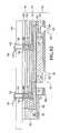
- FIG. 1is a perspective view showing an exemplary membrane probing assembly bolted to a probe head and a wafer supported on a chuck in suitable position for probing by this assembly.
- FIG. 2is a bottom plan view showing various parts of the probing assembly of FIG. 1 , including a support element and flexible membrane assembly, and a fragmentary view of a probe card having power, and data/signal lines connected with corresponding lines on the membrane assembly.
- FIG. 3is a side elevation view of the membrane probing assembly of FIG. 1 where a portion of the membrane assembly has been cut away to expose hidden portions of the support element.
- FIG. 4is a schematic sectional elevation view of an exemplary probing assembly.
- FIG. 5is a top plan view of an exemplary support element.
- FIG. 6is a bottom plan view of an exemplary coupon.
- FIG. 7is a sectional view of a membrane and coupon taken along line 7 - 7 of FIG. 6 .
- FIG. 8is a sectional view of a membrane and coupon taken along line 8 - 8 of FIG. 6 .
- FIG. 9is a sectional view of a membrane and coupon illustrating connection to a conductor extending through the forward support.
- FIG. 10is a sectional view of a membrane and coupon illustrating an alternative method of connecting a contact and a membrane supported trace.
- FIG. 11is a sectional view of a membrane and coupon illustrating an alternative method of connecting a contact and a membrane supported trace.
- FIG. 12is a sectional view of a coupon useful with a space transformer of a needle card-type probing apparatus.
- FIG. 13is a sectional view of additional embodiments of contacts for a coupon useful with a membrane probing device.
- FIG. 14is a bottom plan view of a multi-layered tile portion of a coupon.
- FIG. 15is a sectional view of the multi-layered tile of FIG. 14 taken along line 15 - 15 .
- FIG. 16is a sectional view of the multi-layered tile of FIG. 14 taken along line 16 - 16 .
- FIG. 17is a top view of a portion of an exemplary interface board and an impedance optimized co-axial cable to co-planar waveguide interface.
- FIG. 18is a sectional view of the exemplary co-axial cable to co-planar waveguide interface taken along line 18 - 18 of FIG. 17 .
- FIG. 19is a top view of an alternative impedance optimized co-axial cable to co-planar waveguide interface.
- a probe head 40 for mounting a membrane probing assembly 42is illustrated.
- DUTelectrical circuit or device-under-test
- input and output ports of the test instrumentation 49are communicatively connected to contacts 81 included on the lower portion of the membrane probing assembly and the chuck 51 which supports the wafer is moved in mutually perpendicular X, Y, and Z directions in order to bring bond pads of the DUT into pressing engagement with the probe's contacts.
- the probe head 40includes an interface board 52 on which traces 48 and shielded transmission lines are arranged for communicating data, signals and power between the test instrumentation and the DUT.
- high frequency signalsare communicated between the test instrumentation and the probe with co-axial cables 53 which connect the instrumentation to co-axial cable adapters 55 on the interface board.
- the shielded transmission linestypically comprising second lengths of co-axial cable 50 connect the adapters to metallic traces 87 on the interface board to transition the communication path from the coaxial cable to a co-planar waveguide.
- contact portions 86 that terminate conductors on surface of the membraneare arranged to overlap and conductively interconnect with the traces on the interface board extending the co-planar waveguide from the interface board to the lower surface of the membrane assembly in the vicinity of the contacts and, eventually, to appropriate contacts 81 of the probing apparatus.
- the membrane probing assembly 42includes a support element 54 formed of incompressible material such as a transparent, hard polymer.
- This elementis detachably connected to the upper side of the interface board by means of four Allen screws 56 and corresponding nuts 58 (each screw passes through a respective attachment arm 60 of the support element, and a separate backing element 62 that evenly distributes the clamping pressure of the screws over the entire back side of the supporting element).
- This detachable connectionenables different membrane assemblies having different arrangements of conductors to be quickly substituted for each other as needed for probing different devices.
- a transparent window 63enables an operator of the probing apparatus to view the portion of the wafer in the vicinity of the probe contacts 81 .
- the support element 54includes a rearward base portion 64 to which the attachment arms 60 are integrally joined. Also included on the support element 54 is a forward support or plunger 66 that projects outwardly from the flat base portion. This forward support has angled sides 68 that converge toward a flat support surface 70 so as to give the forward support the shape of a truncated pyramid.
- a flexible membrane assembly 72is attached to the support after being aligned by means of alignment pins 74 included on the base portion.
- This flexible membrane assemblyis formed by one or more plies of insulating sheeting such as KAPTONTM polyimide film sold by E.I. Du Pont de Nemours or other polyimide film, and flexible conductive layers or strips are provided on the surfaces of the plies or between the plies to form various conductors connecting the probe's contacts with the traces and shielded transmission lines on the interface board.
- the forward support 66protrudes through a central opening 78 in the interface board so as to present the contacts 81 which are arranged on a coupon 80 that is attached to the surface of the membrane assembly 72 in a position suitable for pressing engagement with the pads of the DUT.
- the membrane assemblyincludes radially extending arm segments 82 that are separated by inwardly curving edges 84 that give the assembly the shape of a formee cross, and these segments extend in an inclined manner along the angled sides 68 thereby clearing any upright components surrounding the pads.
- a series of contact pads 86terminate the conductors of the membrane so that when the support element is mounted, these pads electrically engage corresponding termination pads provided on the upper side of the interface board so that the traces 48 and shielded transmission lines 50 on the interface board are conductively connected to the contacts 81 on the coupon 80 .
- the exemplary membrane probing assembly 42is capable of probing a dense arrangement of contact pads over a large number of contact cycles in a manner that ensures reliable electrical connection between the contacts and pads during each cycle despite oxide buildup on the pads.
- This capabilityis a function of the construction and interconnection of the support element 54 , the flexible membrane assembly 72 and the coupon 80 .
- the membrane probing assemblyis so constructed and connected to the support element to enable the contacts to engage a plurality of bond pads on the DUT even if the contact surfaces of the pads are not co-planar.
- the contacts on the membrane assemblypreferably wipe or scrub, in a locally controlled manner, laterally across the pads when brought into pressing engagement with the pads.
- the contactsmay be constructed to enable the tips of the contacts to penetrate an oxide coating on the surfaces of the pads with substantially vertical motion.
- the contactsrequire replacement due to, for examples, a built up of pad material, wear, or a change in the arrangement of the pads to be probed, the contacts can be easily replaced by removing and replacing the coupon without the added expense of replacing the membrane assembly.
- an exemplary flexible membrane assembly 72(indicated by a bracket) comprises one or more traces 76 affixed to an outer surface of a ply 92 comprising a dielectric material which is separated by a backplane conductive layer 94 from a second dielectric ply 96 .
- additional dielectric plies and conductive layerscan be used in accordance with conventional layering techniques.
- the conductors of the backplane layer and the other tracesare fabricated using a photolithographic process to enable precise control of the dimensions of the conductors.
- the membrane assemblyis secured along its edges and extends over the flat support surface 70 of the plunger 66 .
- the plurality of traces 76 affixed to the outer surface of the membrane assemblyprovide communication paths for conducting data/signals and/or power from the conductors at the interface board to the surface of the membrane proximate the forward surface of the plunger.
- the conductive traces on the outer surface of the membrane assemblycomprise controlled impedance communication structures connecting the interface board to the surface of the membrane in the vicinity of the forward surface of the plunger.
- the backplane conductive layer 94may include portions defining one or more apertures which, in turn, define conductive strips of the backplane layer that are located proximate the various traces 76 on the outer surface of the membrane assembly.
- Filter capacitors 83may be affixed to the membrane to provide frequency dependent interconnection between the conductive backplane layer and the power and signal conductors.
- FIG. 8shows an enlarged plan view of the lower surface of an exemplary coupon 80 that is attachable to the lower surface of the membrane 72 in area of the forward support surface 70 of the plunger.
- the couponis attached to the surface of the membrane by an adhesive 95 that enables removal of the coupon by breaking the adhesive bond.
- the adhesivemay be applied proximate the periphery of the coupon, at particular locations on the surface or as layer that substantially covers the surface of the coupon but which is displaced from the points of electrical contact by pressure applied to the lower surface of the coupon.
- the couponincludes a plurality of contacts 81 which in the illustrated exemplary embodiment are arranged in a square pattern suitable for engaging a square-like arrangement of bond pads. Referring also to FIGS.
- the couponcomprises an elastomeric layer 98 that is substantially co-extensive with the exposed surface of the portion of the membrane that covers the forward support surface 70 of the plunger.
- the elastomeric layercan be formed by a silicon rubber compound such as ELMER'S STICK-ALLTM silicon rubber made by the Borden Company or Sylgard 182 silicon rubber from Dow Corning Corporation.
- Each contactcomprises a relatively thick rigid elongate beam 100 , preferably 150 to 250 microns long, having an upper surface that is affixed to the elastomeric layer.
- a contact tip 102 having the general shape of a truncated pyramidis formed.
- the contact tipmay include a tip end portion 104 comprising an alloy of rhodium and nickel.
- a post portion 106projects in the direction opposite of the contact tip.
- the post 106projects through the elastomeric layer and, preferably, projects proud of the upper surface of the coupon.
- the posts of selected contactsare arranged for conductive contact with one of the traces 76 on the outer surface of the membrane. As illustrated in FIG.
- the posts of other contactsare arranged for conductive contact with contact buttons 108 projecting from the backplane conductive layer 94 through the lower ply 92 of the membrane assembly.
- Additional dielectric layersfor example layer 112 , may be affixed to the lower surface of the elastic layer.
- the effectis such as to cause the tip of the contact to translate across the pad in a lateral scrubbing movement with a solid-line and a dashed-line representing the beginning 102 and ending positions 102 ′, respectively, of the contact tip on the pad 110 which, after displacement relative to the coupon, will be in position 110 ′.
- the insulating oxide buildup on the padis abraded so as to provide reliable probe contact-to-bond pad electrical connections.
- the movement of the contactdoes not cause flexing of the trace or other conductor of the membrane which substantially reducing fatigue of the conductors and extending the service life of the membrane.
- the power transmissible on the traces deposited on the plies of the flexible membraneis limited by the cross-section of the traces. As a result, extremely wide traces or large numbers of traces may be required to provide sufficient power to operate the electrical circuits of a DUT or a plurality of DUTs.
- the probing assembly 42includes a power conductor 114 that is routed through the support 66 to a contact button 116 that extends through the lower wall of the forward support surface 70 .
- the contact buttonconductively engages a buss 118 , which may comprise a grid, On the upper surface of the membrane 72 .
- the bussis extended downward to the lower surface of the membrane through apertures 119 in the other layers of the membrane.
- Selected contacts 81include post portions that engage the buss extensions to provide power to the appropriate bond pad(s) of the DUT(s).
- the busscan have a substantially greater cross-section than the other conductors on the membrane because it is not located in an area of the membrane where flexibility is required.
- the resilient elastomeric layer 98 of the couponbacked by the incompressible support surface 70 and the substantially incompressible membrane 72 , exerts a recovery force on each tilting beam contact and thus each contact tip to maintain an adequate level of contact tip-to-bond pad pressure during scrubbing.
- the elastomeric layeraccommodates minor height variations between the respective contacts and pads.
- deformation of the elastomeric layerenables the shorter contact to be brought into engagement with its pad after only a small amount of further over travel by the longer contact tips.
- the compressibility of the elastomeric layerenables the contact tips to be brought into proper pressing engagement with a plurality of bond pads having surfaces that are not co-planar.
- the contacts 120may comprise an elongate beam portion 122 affixed to the elastically supported lower surface of the elastomer layer 98 .
- the contact tip portion 102is affixed proximate one end of the beam portion.
- the lower surface of the elastomer layeris displaced proximate the end of the beam to which the tip is affixed, but the elastic force exerted at other end of the beam causes the beam to tilt facilitating the scrubbing action when the tip is pressed toward the bond pad of the DUT.
- the contact 120is conductively connected to one of the traces 76 or the backplane layer 94 by a flexible conductive pigtail 124 .
- the conductive pigtailmay terminate on the surface of the elastomeric layer at a location suitable for contact with a trace 76 or a contact button 108 or maybe conductively connected with a contact pad 126 suitably located on the surface of the coupon for contact with the appropriate trace or contact button.
- FIG. 12illustrates a coupon 150 (indicated by a bracket) having a plurality of elastomer suspended contacts that is suitable for use with components of a needle card-type probe head enabling the needle card-type probing assembly to be converted to a lower inductance probing assembly with elastically suspended contacts by removing the needle card-type probe head and replacing it with the coupon 150 that interfaces with a space transformer 152 (indicated with a bracket) of the needle card-type probing apparatus.
- the size of certain elements and componentsare exaggerated, for illustrative clarity.
- the interface board 154 of the needle card-type probing assemblyis generally a conventional circuit board substrate having a plurality of terminals 156 (two of many shown) disposed on a surface thereof.
- the terminalsprovide an interface for wires 158 that connect instrumentation (not shown) to the probing assembly.
- the wiresmay be connected to terminals on one side of the interface board which are, in turn, connected by conductive vias 160 to terminals 162 or traces on the opposing side of the interface board.
- Additional components(not shown), such as active and passive electronic components, connectors, and the like, may be mounted on the interface board and connected to additional terminals.
- the interface boardis typically round and commonly has a diameter on the order of 12 inches.
- the terminals 156 , 162 on the interface boardare often arranged at a 100 mil pitch or separation distance.
- the exemplary probing assembly of FIG. 12includes an interposer 164 (indicated by a bracket) disposed between the interface board and the space transformer.
- An interposercomprises interconnected electrical contacts disposed on opposing sides of a substrate so that components on opposing sides of the substrate can be conductively interconnected.
- An interposeris often used in a probing assembly to facilitate reliable conductive connection between the terminals of an interface board and the terminals of a space transformer. The interposer also aids in accommodating differences in thermal expansion of the interface board and the space transformer.
- the interposer 164comprises a substrate 166 and a plurality of fuzz buttons 168 (two are shown) that protrude through holes in the substrate.
- the fuzz buttonseach comprise a fine wire that is compressed into a small cylindrical shape to produce an electrically conductive, elastic wire mass.
- the fuzz buttonsare arranged at a pitch which matches that of the terminals 162 of the interface board.
- One end of each of the conductive fuzz buttonsis in contact with a terminal on the interface board while the second end of the fuzz button is in contact with a terminal 170 on the space transformer.
- the elastic fuzz buttonsare compressed providing compliance to accommodate variations in the separation distances between of the various terminals of the interface board and the space transformer and exerting pressure on the contacts to promote good conductivity.
- the space transformer 154(indicated by a bracket) comprises a suitably circuited substrate 172 , such as a multi-layer ceramic substrate having a plurality of terminals (contact areas, pads) 170 (two of many shown) disposed on the surface adjacent to the interposer and a plurality of terminals 174 (contact areas, pads) (two of many shown) disposed on the opposing surface.
- the contact pads adjacent the interposerare disposed at the pitch of the terminals of the interface board, and the contact pads 174 arranged on the opposing surface of the space transformer are disposed at a finer pitch corresponding to the pitch and arrangement of the needle-type probes included in the needle card with which the space transformer was intended to interface.
- the pitch of the terminals of the interface boardis commonly approximately 100 mil
- the pitch of needle-type probescan be as fine as approximately 125 ⁇ m.
- Conductive traces 176 in the multilayer substrate of the space transformerre-route the electrical connections from the finely pitched pattern required to interface with the probe head to the more coarsely pitched pattern that is obtainable with a printed circuit board, such as the interface board.
- the probing assemblyincludes a rigid front mounting plate 180 arranged on one side of the interface board.
- a stand-off 182 with a central aperture to receive the space transformeris attached to the front mounting plate.
- a mounting ring 184which is preferably made of a springy material such as phosphor bronze and which may have a pattern of springy tabs extending therefrom, is attachable by screws 186 to the stand-off with the space transformer captured between the mounting ring and the stand-off.
- a coupon 150(indicated by a bracket) comprising an elastomeric layer 190 and a plurality of electrically conductive contacts is affixed to the face of the space transformer, preferably with an adhesive 191 .
- the contactsfor example exemplary contact 192 , may comprise, generally, a relatively thick, elongate, rigid beam portion 194 with a post portion 196 proximate one end of the beam and a contact tip 102 projecting in the opposite direction from the opposite side of the beam proximate the second end of the beam.
- the contact tippreferably has the general shape of a truncated pyramid and the distal end of the contact tip may be coated with a layer of nickel and/or rhodium to provide good electrical conductivity and wear resistant when the contact tip is repeatedly pressed into engagement with the bond pads of DUTs.
- the post 196has a rounded end distal of the beam that abuts a terminal 174 of the space transformer 152 . The rounded end facilitates movable contact between the post and the terminal when the contact tip is displaced upward by interaction with a bond pad.
- Additional dielectric layer(s) 198may be affixed to the lower surface of the elastomeric layer.
- the contact 200exemplifies a second type of contact that may included in the coupon.
- the contact 200comprises a contact tip portion 202 which, preferably, has the shape of a truncated pyramid or cone and a body 204 with, preferably, a square or circular cross-section.
- a shoulder 206may project from the body adjacent to the bottom surface of the elastomeric layer.
- the contactis conductively connected to the upper surface of the coupon 150 by a pig-tail 204 that is conductively attached to the body of the contact at one end and has a second end exposed at the upper surface of the coupon.
- the exposed portion of the pig-tailis arranged to contact a terminal 174 of the space transformer when the coupon is affixed to the surface of the transformer.
- a conductive connection between the contact and the terminal of the space transformermay incorporate a fuzz button, similar to fuzz button 168 , that is embedded in the elastomeric layer with one end exposed at the surface of the coupon and the second end abutting the contact.
- the tip 202 of the contact 200is intended to be pushed through the oxide layer that may develop on the surface of a bond pad and the elasticity of the elastomeric layer may be varied to aid penetration of the oxide layer.
- the body 204 of the contactmay be extended so as to directly contact the terminal of the space transformer, eliminating the need for the pigtail and enabling vertical movement of the contact in response to pressure from the pad to be limited to the deflection of the relatively rigid space transformer while the resiliency of the elastomeric layer may enable the contact to tilt if the surface of the pad is not parallel to the end surface of the tip of the contact.
- the elastomeric layer 190may comprise a single layer with graduated resiliency or a plurality of sub-layers with differing resiliency to enable controlled vertical movement of the contact in response to the application of force at the tip of the contact.
- the couponprovides an economical way of converting a needle-type probing apparatus to a probing apparatus with much lower inductance.
- the relatively long, closely spaced, needle-like probestypically exhibit a single path inductance of 1-2 nano-Henrys (nH) which is sufficient to substantially distort high frequency signals and limit the usefulness of needle-type probes for testing devices with high frequency signals.
- nHnano-Henrys
- single path inductance of 0.2 nHhas been demonstrated with elastically suspended probes of membrane-type probing apparatuses.
- surface penetrating contacts 252 , 254can also be utilized in a coupon 250 (indicated by a bracket) suitable for use with a membrane probing apparatus.
- the contact 254may be rigidly supported by the support 66 and the substantially incompressible membrane assembly 72 .
- the body of the contactis extended through the elastomeric layer 98 so that it abuts the contact button 108 of the backplane layer 94 .
- the abutting end of the contactis rounded enabling tilting of the contact, by compressing the elastomer surrounding the contact's body, to aid in aligning the end of the contact with a non-co-planar pad surface.
- the body of the contact 252terminates in the elastomeric layer and the contact can exhibit elastic behavior as determined by the properties of the elastomer layer.
- the elastomeric layer 98may comprise sub-layers 98 A and 98 B, each having different elastic properties. The elasticity of the contact during vertical displacement may be determined by the properties of the sub-layer 98 A which acts on a portion of the surface area of the upper end of the contact and the properties of sub-layer 98 B which acts on the upper surface of a contact flange 253 .
- a fuzz button 256conductively connects the contact 252 with the trace 76 .
- a coupon 300 for use with a membrane probe or a space transformermay comprise a plurality of coupons or tiles 300 a , 300 b , 300 c , 300 d , each independently detachably affixed to a membrane or a space transformer enabling damaged or worn portions of the coupon to be independently replaced or portions of the coupon to include differing arrangements of contacts 81 . Flexibility in arranging contacts and conductive connections to membranes and space transformers can be facilitated by layering the conductive and non-conductive elements of the coupon.
- the tile 300 cincludes layered circuitry enabling conductive connection of thirteen finely pitched contact tips to a space transformer or membrane having six coarsely pitched contact pads enabling a typically less costly, more coarsely pitched space transformer or membrane to interface with the finely pitched contacts useful for probing small DUTs.
- the tileincludes six grounded contact tips 302 including ground contact tips spaced to each side of a pair of high frequency signal contact tips 304 comprising the terminations of the conductors of a pair of ground-signal-ground (GSG) co-planar waveguides 310 (collectively indicated by a bracket).
- GSGground-signal-ground
- the exemplary tileincludes a pair of contact tips 308 that are arranged to conduct DC power to a DUT and a pair of contact tips 306 that are arranged to conduct a lower frequency signal to the DUT.
- the contacts tips of the couponare affixed to an elastically supported lower surface 314 of an elastomer layer 312 .
- the couponis affixed the lower surface to a space transformer 320 by adhesive 322 .
- the ground contact tips 302are conductively connected to a conductive backplane layer 318 deposited between a pair of dielectric layers 320 and 321 .
- the elastomeric layeris affixed to lower surface of the dielectric layer 321 .
- the backplane layerextends over the area of the coupon that is occupied by the contact tips 302 - 308 .
- the backplane layeris conductively connected to a suitable conductor in the space transformer by a contact button 324 on the upper surface of the coupon which is connected to the backplane layer by a via 326 .
- the contact button 324is arranged to engage a corresponding contact button on the lower surface of the space transformer.
- the contact tips 302include post portions 327 in contact with backplane or a pigtail 328 that conductively connects the side of the beam portion of the contact tip and the back plane layer.
- High frequency signalsare transmitted between the test instrument and the DUT through the high frequency contact tips 304 .
- Each of the high frequency contact tipsis connected to one of a pair of contact buttons 330 on the upper surface of the coupon by a via 332 and a high frequency signal trace 324 that is deposited between the upper surface of the elastomeric layer 312 and the dielectric layer 321 which separates the high frequency trace from the backplane layer.
- the contact tips 308 facilitating the transmission of DC power to the DUTare connected to an appropriate conductor 334 in the space transformer through a contact button 336 on the upper surface of the coupon.
- a trace 338including portions that are conductively affixed to the lower surfaces of the beam portions of the power contact tips 308 , is affixed to the lower surface of a dielectric layer 340 that is, in turn, affixed to the lower surface of the elastomer layer.
- a via 342connects the power trace on the lower surface of the coupon to a contact button 344 on the upper surface of the coupon.
- the coupon 300 calso enables communication of a lower frequency AC signal to the DUT through contact tips 306 which include posts conductively engaging a lower frequency signal layer 346 .
- the lower frequency signalis conducted from the lower frequency signal layer to the space transformer through a via 348 connecting the lower frequency signal layer with a low frequency signal contact button 350 on the upper surface of the coupon.
- a multilayered couponsuch as the coupon 300 including the tile 300 c provides flexibility for connecting an arrangement of finely pitched contact tips with the more coarsely pitched contacts of more moderately priced space transformers.
- the coupon 300also includes one or more forming posts 370 that extend from the upper surface of the elastomer layer 312 to the lower surface of the elastomer layer.
- the forming postsaid in controlling the thickness and in maintaining the planarity of the surfaces of the elastomeric layer during the curing of the elastomer but are not conductively connected to a circuit of the probing apparatus.
- Posts 372extending proud of the surfaces of the coupon are not arranged to conduct electricity but may be provided as an aid for the user in gauging the deflection of the elastically suspended contacts.
- a post 372 having a first end in contact with the space transformer and a second end projecting from the bottom of the coupon a distance slightly less than the height of a contact tipmay serve as a contact gage to prevent damage to the coupon from excess deflection of the elastically supported contact tips.
- an elastically supported post 374 that projects below the lower surface of the couponmay be arranged to provide a signal of the limits of contact tip deflection.
- the conductors of the coaxial cableare first conductively connected to respective traces 87 on the surface of the interface board which collectively comprise an interface board co-planar waveguide.
- the center conductor of the coaxial cableis connected to a center trace and the outer conductor of the cable, which is connected to a ground potential, is connected a pair of side traces, one spaced to either side of the center trace to form a ground-signal-ground (GSG) co-planar waveguide.
- GSGground-signal-ground
- the traces of the interface board co-planar waveguideterminate proximate the edge of the central opening 78 in the interface board and portions of the conductive traces on the membrane's lower surface are arranged to overlap portions of the surfaces of respective traces of the interface board co-planar waveguide when the membrane is clamped to the interface board.
- the overlapping surface portionsconductively interconnect the traces of interface board waveguide to respective traces of a membrane waveguide extending the signal path to the lower surface of the membrane in the region proximate the forward support surface 70 .
- the interface boardincludes a sub-surface conductive layer that is connected to a ground potential to provide a ground plane for the interface board co-planar waveguide.
- a ground potentialto provide a ground plane for the interface board co-planar waveguide.
- inconsistency in the interconnection of the interface board co-planar waveguide and the ground planemay produce an impedance mismatch as the signal path transitions from coaxial cable to co-planar waveguide.
- the inventorsrealized that eliminating the interconnections with the interface board ground plane would eliminate this source of error but would also increase the impedance of the interface board co-planar waveguide to unacceptable levels.
- the inventorscame to the unexpected conclusion that the interface board ground plane could be eliminated by decreasing the gaps between the signal trace and the ground traces of the coplanar waveguide, interconnecting the ground traces of adjacent waveguides and providing a low impedance structure for interconnecting the traces of the membrane and interface board waveguides.
- the exemplary interface board 500includes a plurality of conductive traces deposited on the upper surface.
- Three traces 502 , 504 , 506comprise an interface board co-planar waveguide 508 (indicated by a bracket).
- the center conductor 510 of a coaxial cable 502is conductively interconnected with the center trace 502 of the waveguide and the outer conductor 514 of the cable is connected to a first side trace 504 spaced apart from one edge of the center trace and a second side trace 506 spaced apart from the second edge of the center trace.
- a signalis communicated between the test instrumentation and the probing apparatus over the center conductor of the coaxial cable and the outer conductor is connected to a ground level electrical potential.
- the interface board ground plane 516terminates a substantial distance from the area of the interface board that is overlaid by the traces of the waveguide and is not electrically interconnected with the traces of the waveguide.
- the width of the center trace 502differs from the widths of the side traces and the widths of the respective side traces may also differ from each other.
- the center trace or signal conductor of an exemplary GSG waveguide having an impedance of 50 ⁇is 0.0179 inches wide and is separated from each of the spaced apart side traces of the waveguide by a gap of 0.004 inches.
- a side tracefor example the side trace 506 of the exemplary waveguide is adjacent to the center traces of two waveguides, for example center trace 502 and the center trace 522 of a second waveguide 520 (indicated by a bracket), the side trace is shared by the adjacent waveguides 508 , 512 .
- the side tracepreferably has a width of 0.029 inches and the outer conductors 514 of two adjacent coaxial cables 512 , 526 are conductively connected to the trace.
- a side tracefor example the side trace 504 of the exemplary interface board co-planar waveguide 508 , is adjacent to only one center trace, the side trace has a width of 0.0107 inches.
- the width of the center trace of the interface board waveguidemay be narrowed for the portion of the length that is overlapped by the membrane trace.
- the exemplary waveguide 600includes a central trace 602 comprising a first length portion 604 that is preferably 0.0179 inches wide and a second length portion 606 which is overlapped by the membrane trace 614 and which is preferably 0.0159 inches wide.
- the gap 608 between the center trace and the side traces for the first length portionis 0.004 inches while the gap 610 for the second length portion is 0.005 inches increasing the tolerance to misalignment between the traces of interface and membrane waveguides.
- the impedance of the exemplary waveguide 600is substantially the same as the impedance of a waveguide with uniform 0.004 inch gaps between traces.
- the interconnection of the respective traces of the interface board waveguide and the corresponding traces of the membrane waveguidesubstantially effects the impedance of the waveguide.
- the electro-magnetic fieldis carried in the gap between the traces of a waveguide and the interconnection between the traces can produce a “pinch point” that substantially increases the waveguide's impedance.
- the inventorsconcluded that the more closely the geometry of the interconnecting structure resembles the geometry of the waveguide's traces the lower the impedance of the connection. Referring also to FIG. 18 , when the membrane probe is assembled, contact portions 86 of the traces on the membrane overlap portions of the surfaces of the traces on the interface board.
- the interconnecting structure for the center traces 502 and 530 of the interface board and membrane waveguides, respectively,comprises four pads 540 that project from the surface of one the traces into contact with the surface of the other trace.
- a pair of the raised pads, indicated generally as 542 and 544is arranged substantially parallel to each of the edges of the center trace on which the pads are affixed and the pads are located as close to the edge of the trace as tolerance for misalignment of the trace will allow.
- a raised padis located at each of the corners of a substantially rectangular area on the surface of the trace.
- the side trace 534 on the membraneoverlaps a portion of the side trace 504 on the surface of the interface board 500 and a portion of the membrane side trace 532 overlaps a portion of the interface board waveguide side trace 506 .
- the pair 546 of raised pads 540 nearest the center trace 502are located as close to the inner edge of the trace as is permitted by the tolerance to misalignment and the second pair 548 of raised pads are preferably located nearer the center line of the membrane trace than the second edge of the trace.
- the electro-magnetic fieldis carried in the region between the traces of the waveguide and locating the pads of interconnecting structure closer to the region in which the electro-magnetic field is confined reduces the inductance of the connection.
- the accuracy of measurements performed with the membrane probing apparatusis improved by optimizing the impedance of the interface between co-axial cables, interconnecting the test instrumentation and the probing apparatus, and the co-planar waveguide that extends the signal path to the contact tips.
- a longer service life and lower operating cost for a membrane probing apparatusis achievable by including the contact tips on an elastic coupon that is attachable to a membrane that includes a plurality of traces over which signals, data and power can be transmitted.
- Replacing the probe needles of a needle type probing apparatus with a coupon attachable to a space transformer and including elastically supported contact tipscan also improve the performance of a needle-type probing apparatus by substantially lower the inductance of the apparatus.
Landscapes
- Physics & Mathematics (AREA)
- General Physics & Mathematics (AREA)
- Engineering & Computer Science (AREA)
- Mechanical Engineering (AREA)
- Computer Hardware Design (AREA)
- Microelectronics & Electronic Packaging (AREA)
- General Engineering & Computer Science (AREA)
- Measuring Leads Or Probes (AREA)
- Control Of Vending Devices And Auxiliary Devices For Vending Devices (AREA)
Abstract
Description
Claims (16)
Priority Applications (3)
| Application Number | Priority Date | Filing Date | Title |
|---|---|---|---|
| US12/592,186US8410806B2 (en) | 2008-11-21 | 2009-11-20 | Replaceable coupon for a probing apparatus |
| US13/854,725US9429638B2 (en) | 2008-11-21 | 2013-04-01 | Method of replacing an existing contact of a wafer probing assembly |
| US15/222,113US10267848B2 (en) | 2008-11-21 | 2016-07-28 | Method of electrically contacting a bond pad of a device under test with a probe |
Applications Claiming Priority (2)
| Application Number | Priority Date | Filing Date | Title |
|---|---|---|---|
| US19991008P | 2008-11-21 | 2008-11-21 | |
| US12/592,186US8410806B2 (en) | 2008-11-21 | 2009-11-20 | Replaceable coupon for a probing apparatus |
Related Child Applications (1)
| Application Number | Title | Priority Date | Filing Date |
|---|---|---|---|
| US13/854,725ContinuationUS9429638B2 (en) | 2008-11-21 | 2013-04-01 | Method of replacing an existing contact of a wafer probing assembly |
Publications (2)
| Publication Number | Publication Date |
|---|---|
| US20100127725A1 US20100127725A1 (en) | 2010-05-27 |
| US8410806B2true US8410806B2 (en) | 2013-04-02 |
Family
ID=42195639
Family Applications (3)
| Application Number | Title | Priority Date | Filing Date |
|---|---|---|---|
| US12/592,186Active2031-04-06US8410806B2 (en) | 2008-11-21 | 2009-11-20 | Replaceable coupon for a probing apparatus |
| US13/854,725Active2031-05-20US9429638B2 (en) | 2008-11-21 | 2013-04-01 | Method of replacing an existing contact of a wafer probing assembly |
| US15/222,113ActiveUS10267848B2 (en) | 2008-11-21 | 2016-07-28 | Method of electrically contacting a bond pad of a device under test with a probe |
Family Applications After (2)
| Application Number | Title | Priority Date | Filing Date |
|---|---|---|---|
| US13/854,725Active2031-05-20US9429638B2 (en) | 2008-11-21 | 2013-04-01 | Method of replacing an existing contact of a wafer probing assembly |
| US15/222,113ActiveUS10267848B2 (en) | 2008-11-21 | 2016-07-28 | Method of electrically contacting a bond pad of a device under test with a probe |
Country Status (2)
| Country | Link |
|---|---|
| US (3) | US8410806B2 (en) |
| WO (1) | WO2010059247A2 (en) |
Cited By (12)
| Publication number | Priority date | Publication date | Assignee | Title |
|---|---|---|---|---|
| US20130044033A1 (en)* | 2011-08-17 | 2013-02-21 | Joshua G. Nickel | Test system with adjustable radio-frequency probe array |
| US20140055157A1 (en)* | 2010-04-21 | 2014-02-27 | Shinko Electric Industries Co., Ltd. | Probe card and method for manufacturing probe card |
| US20160084905A1 (en)* | 2014-09-24 | 2016-03-24 | Micron Technology, Inc. | Apparatus for testing stacked die assemblies, and related methods |
| US9435855B2 (en) | 2013-11-19 | 2016-09-06 | Teradyne, Inc. | Interconnect for transmitting signals between a device and a tester |
| US9594114B2 (en) | 2014-06-26 | 2017-03-14 | Teradyne, Inc. | Structure for transmitting signals in an application space between a device under test and test electronics |
| US9977052B2 (en) | 2016-10-04 | 2018-05-22 | Teradyne, Inc. | Test fixture |
| US10120020B2 (en) | 2016-06-16 | 2018-11-06 | Formfactor Beaverton, Inc. | Probe head assemblies and probe systems for testing integrated circuit devices |
| US20180340861A1 (en)* | 2017-05-23 | 2018-11-29 | Fluke Corporation | Measuring optical array polarity, power, and loss using a position sensing detector and photodetector-equipped optical testing device |
| US10677815B2 (en) | 2018-06-08 | 2020-06-09 | Teradyne, Inc. | Test system having distributed resources |
| RU2730888C1 (en)* | 2019-12-16 | 2020-08-26 | Акционерное общество "НПО "Орион" | Method for manufacturing rigid probe heads |
| US11363746B2 (en) | 2019-09-06 | 2022-06-14 | Teradyne, Inc. | EMI shielding for a signal trace |
| US11862901B2 (en) | 2020-12-15 | 2024-01-02 | Teradyne, Inc. | Interposer |
Families Citing this family (9)
| Publication number | Priority date | Publication date | Assignee | Title |
|---|---|---|---|---|
| KR101108726B1 (en)* | 2010-01-26 | 2012-02-29 | 삼성전기주식회사 | Member for adjusting horizontality |
| US8970240B2 (en) | 2010-11-04 | 2015-03-03 | Cascade Microtech, Inc. | Resilient electrical interposers, systems that include the interposers, and methods for using and forming the same |
| US9244099B2 (en) | 2011-05-09 | 2016-01-26 | Cascade Microtech, Inc. | Probe head assemblies, components thereof, test systems including the same, and methods of operating the same |
| JP6496142B2 (en)* | 2014-12-26 | 2019-04-03 | 株式会社ヨコオ | Replacement contact unit and inspection jig |
| WO2018035054A1 (en)* | 2016-08-16 | 2018-02-22 | Translarity, Inc. | Space transformers for probe cards, and associated systems and methods |
| WO2023009077A1 (en)* | 2021-07-26 | 2023-02-02 | Minkon Tekstil Sanayi Ve Dis Ticaret Limited Sirketi | Twin-probe electrical tester used in high-voltage transmission lines |
| JP2023047464A (en)* | 2021-09-27 | 2023-04-06 | 株式会社ヨコオ | Contact unit and inspection jig |
| KR102731416B1 (en)* | 2022-08-18 | 2024-11-19 | 주식회사 코비스테크놀로지 | Micro wafer probe, apparatus for measuring electrial properties of wafer using microwafer probe and method using the same |
| US12306243B2 (en) | 2023-06-12 | 2025-05-20 | Formfactor, Inc. | Space transformers configured to be utilized in a probe system, probe systems that include the space transformers, and related methods |
Citations (875)
| Publication number | Priority date | Publication date | Assignee | Title |
|---|---|---|---|---|
| US1337866A (en) | 1917-09-27 | 1920-04-20 | Griffiths Ethel Grace | System for protecting electric cables |
| US2142625A (en) | 1932-07-06 | 1939-01-03 | Hollandsche Draad En Kabelfab | High tension cable |
| US2376101A (en) | 1942-04-01 | 1945-05-15 | Ferris Instr Corp | Electrical energy transmission |
| US2389668A (en) | 1943-03-04 | 1945-11-27 | Barnes Drill Co | Indexing mechanism for machine tables |
| US3176091A (en) | 1962-11-07 | 1965-03-30 | Helmer C Hanson | Controlled multiple switching unit |
| US3193712A (en) | 1962-03-21 | 1965-07-06 | Clarence A Harris | High voltage cable |
| US3230299A (en) | 1962-07-18 | 1966-01-18 | Gen Cable Corp | Electrical cable with chemically bonded rubber layers |
| US3401126A (en) | 1965-06-18 | 1968-09-10 | Ibm | Method of rendering noble metal conductive composition non-wettable by solder |
| US3429040A (en) | 1965-06-18 | 1969-02-25 | Ibm | Method of joining a component to a substrate |
| US3441315A (en) | 1967-07-07 | 1969-04-29 | Artnell Co | Seat and method for manufacturing the same |
| US3442831A (en) | 1966-04-21 | 1969-05-06 | Borden Co | Vinyl chloride polymerization process and latex |
| US3445770A (en) | 1965-12-27 | 1969-05-20 | Philco Ford Corp | Microelectronic test probe with defect marker access |
| US3484679A (en) | 1966-10-03 | 1969-12-16 | North American Rockwell | Electrical apparatus for changing the effective capacitance of a cable |
| US3541222A (en) | 1969-01-13 | 1970-11-17 | Bunker Ramo | Connector screen for interconnecting adjacent surfaces of laminar circuits and method of making |
| US3595228A (en) | 1968-11-27 | 1971-07-27 | Robert C Simon | Flow line break alarm device |
| US3596228A (en) | 1969-05-29 | 1971-07-27 | Ibm | Fluid actuated contactor |
| US3609539A (en) | 1968-09-28 | 1971-09-28 | Ibm | Self-aligning kelvin probe |
| US3634807A (en) | 1969-03-28 | 1972-01-11 | Siemens Ag | Detachable electrical contact arrangement |
| US3654585A (en) | 1970-03-11 | 1972-04-04 | Brooks Research And Mfg Inc | Coordinate conversion for the testing of printed circuit boards |
| US3680037A (en) | 1970-11-05 | 1972-07-25 | Tech Wire Prod Inc | Electrical interconnector |
| US3700998A (en) | 1970-08-20 | 1972-10-24 | Computer Test Corp | Sample and hold circuit with switching isolation |
| US3710251A (en) | 1971-04-07 | 1973-01-09 | Collins Radio Co | Microelectric heat exchanger pedestal |
| US3714572A (en) | 1970-08-21 | 1973-01-30 | Rca Corp | Alignment and test fixture apparatus |
| US3740900A (en) | 1970-07-01 | 1973-06-26 | Signetics Corp | Vacuum chuck assembly for semiconductor manufacture |
| US3806801A (en) | 1972-12-26 | 1974-04-23 | Ibm | Probe contactor having buckling beam probes |
| US3829076A (en) | 1972-06-08 | 1974-08-13 | H Sofy | Dial index machine |
| US3839672A (en) | 1973-02-05 | 1974-10-01 | Belden Corp | Method and apparatus for measuring the effectiveness of the shield in a coaxial cable |
| US3849728A (en) | 1973-08-21 | 1974-11-19 | Wentworth Labor Inc | Fixed point probe card and an assembly and repair fixture therefor |
| US3858212A (en) | 1972-08-29 | 1974-12-31 | L Tompkins | Multi-purpose information gathering and distribution system |
| US3862790A (en) | 1971-07-22 | 1975-01-28 | Plessey Handel Investment Ag | Electrical interconnectors and connector assemblies |
| US3866093A (en) | 1972-09-18 | 1975-02-11 | Norbert L Kusters | Low leakage electrical power input circuit for electromedical and other similar apparatus |
| US3936743A (en) | 1974-03-05 | 1976-02-03 | Electroglas, Inc. | High speed precision chuck assembly |
| US3952156A (en) | 1972-09-07 | 1976-04-20 | Xerox Corporation | Signal processing system |
| US3970934A (en) | 1974-08-12 | 1976-07-20 | Akin Aksu | Printed circuit board testing means |
| US3971610A (en) | 1974-05-10 | 1976-07-27 | Technical Wire Products, Inc. | Conductive elastomeric contacts and connectors |
| US3976959A (en) | 1974-07-22 | 1976-08-24 | Gaspari Russell A | Planar balun |
| US3992073A (en) | 1975-11-24 | 1976-11-16 | Technical Wire Products, Inc. | Multi-conductor probe |
| US4008900A (en) | 1976-03-15 | 1977-02-22 | John Freedom | Indexing chuck |
| US4027935A (en) | 1976-06-21 | 1977-06-07 | International Business Machines Corporation | Contact for an electrical contactor assembly |
| US4038599A (en) | 1974-12-30 | 1977-07-26 | International Business Machines Corporation | High density wafer contacting and test system |
| US4038894A (en) | 1975-07-18 | 1977-08-02 | Springfield Tool And Die, Inc. | Piercing apparatus |
| US4049252A (en) | 1976-02-04 | 1977-09-20 | Bell Theodore F | Index table |
| US4072576A (en) | 1975-10-06 | 1978-02-07 | Ab Kabi | Method for studying enzymatic and other biochemical reactions |
| US4093988A (en) | 1976-11-08 | 1978-06-06 | General Electric Company | High speed frequency response measurement |
| US4099120A (en) | 1976-04-19 | 1978-07-04 | Akin Aksu | Probe head for testing printed circuit boards |
| US4115735A (en) | 1976-10-14 | 1978-09-19 | Faultfinders, Inc. | Test fixture employing plural platens for advancing some or all of the probes of the test fixture |
| US4135131A (en) | 1977-10-14 | 1979-01-16 | The United States Of America As Represented By The Secretary Of The Army | Microwave time delay spectroscopic methods and apparatus for remote interrogation of biological targets |
| US4184729A (en) | 1977-10-13 | 1980-01-22 | Bunker Ramo Corporation | Flexible connector cable |
| US4275446A (en) | 1978-11-13 | 1981-06-23 | Siemens Aktiengesellschaft | Method and apparatus for measurement of attenuation and distortion by a test object |
| SU843040A1 (en) | 1979-08-06 | 1981-06-30 | Физико-Технический Институт Низкихтемператур Ah Украинской Ccp | Straightway rejection filter |
| US4277741A (en) | 1979-06-25 | 1981-07-07 | General Motors Corporation | Microwave acoustic spectrometer |
| US4284033A (en) | 1979-10-31 | 1981-08-18 | Rca Corporation | Means to orbit and rotate target wafers supported on planet member |
| US4284682A (en) | 1980-04-30 | 1981-08-18 | Nasa | Heat sealable, flame and abrasion resistant coated fabric |
| US4287473A (en) | 1979-05-25 | 1981-09-01 | The United States Of America As Represented By The United States Department Of Energy | Nondestructive method for detecting defects in photodetector and solar cell devices |
| US4306235A (en) | 1978-11-02 | 1981-12-15 | Cbc Corporation | Multiple frequency microwave antenna |
| US4312117A (en) | 1977-09-01 | 1982-01-26 | Raytheon Company | Integrated test and assembly device |
| US4327180A (en) | 1979-09-14 | 1982-04-27 | Board Of Governors, Wayne State Univ. | Method and apparatus for electromagnetic radiation of biological material |
| US4330783A (en) | 1979-11-23 | 1982-05-18 | Toia Michael J | Coaxially fed dipole antenna |
| US4357575A (en) | 1980-06-17 | 1982-11-02 | Dit-Mco International Corporation | Apparatus for use in testing printed circuit process boards having means for positioning such boards in proper juxtaposition with electrical contacting assemblies |
| US4376920A (en) | 1981-04-01 | 1983-03-15 | Smith Kenneth L | Shielded radio frequency transmission cable |
| US4383217A (en) | 1979-01-02 | 1983-05-10 | Shiell Thomas J | Collinear four-point probe head and mount for resistivity measurements |
| US4401945A (en) | 1981-04-30 | 1983-08-30 | The Valeron Corporation | Apparatus for detecting the position of a probe relative to a workpiece |
| US4425395A (en) | 1981-04-30 | 1984-01-10 | Fujikura Rubber Works, Ltd. | Base fabrics for polyurethane-coated fabrics, polyurethane-coated fabrics and processes for their production |
| US4453142A (en) | 1981-11-02 | 1984-06-05 | Motorola Inc. | Microstrip to waveguide transition |
| US4468629A (en) | 1982-05-27 | 1984-08-28 | Trw Inc. | NPN Operational amplifier |
| US4487996A (en) | 1982-12-02 | 1984-12-11 | Electric Power Research Institute, Inc. | Shielded electrical cable |
| US4515439A (en) | 1982-01-27 | 1985-05-07 | Carl-Zeiss-Stiftung, Heidenheim/Brenz | Attachment of microscope objectives |
| US4515133A (en) | 1984-05-31 | 1985-05-07 | Frank Roman | Fuel economizing device |
| US4528504A (en) | 1982-05-27 | 1985-07-09 | Harris Corporation | Pulsed linear integrated circuit tester |
| US4531474A (en) | 1983-06-04 | 1985-07-30 | Dainippon Screen Manufacturing Co., Ltd. | Rotary board treating apparatus |
| US4552033A (en) | 1980-07-08 | 1985-11-12 | Gebr. Marzhauser Wetzlar oHG | Drive system for a microscope stage or the like |
| US4567321A (en) | 1984-02-20 | 1986-01-28 | Junkosha Co., Ltd. | Flexible flat cable |
| US4568890A (en) | 1982-12-23 | 1986-02-04 | U.S. Philips Corporation | Microwave oscillator injection locked at its fundamental frequency for producing a harmonic frequency output |
| US4581679A (en) | 1983-05-31 | 1986-04-08 | Trw Inc. | Multi-element circuit construction |
| US4588950A (en) | 1983-11-15 | 1986-05-13 | Data Probe Corporation | Test system for VLSI digital circuit and method of testing |
| US4593243A (en) | 1984-08-29 | 1986-06-03 | Magnavox Government And Industrial Electronics Company | Coplanar and stripline probe card apparatus |
| US4600907A (en) | 1985-03-07 | 1986-07-15 | Tektronix, Inc. | Coplanar microstrap waveguide interconnector and method of interconnection |
| US4621169A (en) | 1983-06-21 | 1986-11-04 | Compagnie Francaise De Raffinage | Electric cable construction and uses therefor |
| US4626618A (en) | 1984-05-08 | 1986-12-02 | Fujikura Ltd. | DC electric power cable |
| US4636772A (en) | 1985-01-17 | 1987-01-13 | Riken Denshi Co. Ltd. | Multiple function type D/A converter |
| US4636722A (en) | 1984-05-21 | 1987-01-13 | Probe-Rite, Inc. | High density probe-head with isolated and shielded transmission lines |
| US4641659A (en) | 1979-06-01 | 1987-02-10 | Sepponen Raimo E | Medical diagnostic microwave scanning apparatus |
| US4642417A (en) | 1984-07-30 | 1987-02-10 | Kraftwerk Union Aktiengesellschaft | Concentric three-conductor cable |
| US4646005A (en) | 1984-03-16 | 1987-02-24 | Motorola, Inc. | Signal probe |
| US4649339A (en) | 1984-04-25 | 1987-03-10 | Honeywell Inc. | Integrated circuit interface |
| US4651115A (en) | 1985-01-31 | 1987-03-17 | Rca Corporation | Waveguide-to-microstrip transition |
| US4663840A (en) | 1984-12-11 | 1987-05-12 | U.S. Philips Corporation | Method of interconnecting conductors of different layers of a multilayer printed circuit board |
| US4673839A (en) | 1986-09-08 | 1987-06-16 | Tektronix, Inc. | Piezoelectric pressure sensing apparatus for integrated circuit testing stations |
| EP0230348A2 (en) | 1986-01-07 | 1987-07-29 | Hewlett-Packard Company | Test probe |
| US4684883A (en) | 1985-05-13 | 1987-08-04 | American Telephone And Telegraph Company, At&T Bell Laboratories | Method of manufacturing high-quality semiconductor light-emitting devices |
| US4691163A (en) | 1985-03-19 | 1987-09-01 | Elscint Ltd. | Dual frequency surface probes |
| US4697143A (en) | 1984-04-30 | 1987-09-29 | Cascade Microtech, Inc. | Wafer probe |
| US4705447A (en) | 1983-08-11 | 1987-11-10 | Intest Corporation | Electronic test head positioner for test systems |
| US4707657A (en) | 1984-06-13 | 1987-11-17 | Boegh Petersen Allan | Connector assembly for a circuit board testing machine, a circuit board testing machine, and a method of testing a circuit board by means of a circuit board testing machine |
| US4711563A (en) | 1987-02-11 | 1987-12-08 | Lass Bennett D | Portable collapsible darkroom |
| US4713347A (en) | 1985-01-14 | 1987-12-15 | Sensor Diagnostics, Inc. | Measurement of ligand/anti-ligand interactions using bulk conductance |
| US4719417A (en)* | 1983-05-03 | 1988-01-12 | Wentworth Laboratories, Inc. | Multi-level test probe assembly for IC chips |
| US4725793A (en) | 1985-09-30 | 1988-02-16 | Alps Electric Co., Ltd. | Waveguide-microstrip line converter |
| US4727391A (en) | 1986-01-24 | 1988-02-23 | Fuji Photo Film Co., Ltd., | Sheet film package and device for loading sheet films |
| US4727637A (en) | 1987-01-20 | 1988-03-01 | The Boeing Company | Computer aided connector assembly method and apparatus |
| SU1392603A1 (en) | 1982-11-19 | 1988-04-30 | Физико-технический институт низких температур АН УССР | Band-rejection filter |
| US4742571A (en) | 1985-07-23 | 1988-05-03 | Thomson-Csf | Coupling device between a metal wave guide, a dielectric wave guide and a semiconductor component and a mixer using this coupling device |
| US4744041A (en) | 1985-03-04 | 1988-05-10 | International Business Machines Corporation | Method for testing DC motors |
| US4746857A (en) | 1985-09-13 | 1988-05-24 | Danippon Screen Mfg. Co. Ltd. | Probing apparatus for measuring electrical characteristics of semiconductor device formed on wafer |
| US4749942A (en) | 1985-09-26 | 1988-06-07 | Tektronix, Inc. | Wafer probe head |
| US4754239A (en) | 1986-12-19 | 1988-06-28 | The United States Of America As Represented By The Secretary Of The Air Force | Waveguide to stripline transition assembly |
| US4755874A (en) | 1987-08-31 | 1988-07-05 | Kla Instruments Corporation | Emission microscopy system |
| US4755747A (en) | 1984-06-15 | 1988-07-05 | Canon Kabushiki Kaisha | Wafer prober and a probe card to be used therewith |
| US4755746A (en) | 1985-04-24 | 1988-07-05 | Prometrix Corporation | Apparatus and methods for semiconductor wafer testing |
| US4757255A (en) | 1986-03-03 | 1988-07-12 | National Semiconductor Corporation | Environmental box for automated wafer probing |
| US4766384A (en) | 1986-06-20 | 1988-08-23 | Schlumberger Technology Corp. | Well logging apparatus for determining dip, azimuth, and invaded zone conductivity |
| US4772846A (en) | 1986-12-29 | 1988-09-20 | Hughes Aircraft Company | Wafer alignment and positioning apparatus for chip testing by voltage contrast electron microscopy |
| US4780670A (en) | 1985-03-04 | 1988-10-25 | Xerox Corporation | Active probe card for high resolution/low noise wafer level testing |
| US4791363A (en) | 1987-09-28 | 1988-12-13 | Logan John K | Ceramic microstrip probe blade |
| US4793814A (en) | 1986-07-21 | 1988-12-27 | Rogers Corporation | Electrical circuit board interconnect |
| US4795962A (en) | 1986-09-04 | 1989-01-03 | Hewlett-Packard Company | Floating driver circuit and a device for measuring impedances of electrical components |
| US4805627A (en) | 1985-09-06 | 1989-02-21 | Siemens Aktiengesellschaft | Method and apparatus for identifying the distribution of the dielectric constants in an object |
| EP0304868A2 (en) | 1987-08-28 | 1989-03-01 | Tektronix Inc. | Multiple lead probe for integrated circuits in wafer form |
| US4812754A (en) | 1987-01-07 | 1989-03-14 | Tracy Theodore A | Circuit board interfacing apparatus |
| US4827211A (en) | 1987-01-30 | 1989-05-02 | Cascade Microtech, Inc. | Wafer probe |
| US4831494A (en) | 1988-06-27 | 1989-05-16 | International Business Machines Corporation | Multilayer capacitor |
| US4835495A (en) | 1988-04-11 | 1989-05-30 | Hughes Aircraft Company | Diode device packaging arrangement |
| US4837507A (en) | 1984-06-08 | 1989-06-06 | American Telephone And Telegraph Company At&T Technologies, Inc. | High frequency in-circuit test fixture |
| US4839587A (en) | 1988-03-29 | 1989-06-13 | Digital Equipment Corporation | Test fixture for tab circuits and devices |
| EP0259163A3 (en) | 1986-09-05 | 1989-07-12 | Tektronix, Inc. | Semiconductor wafer probe |
| US4849689A (en) | 1988-11-04 | 1989-07-18 | Cascade Microtech, Inc. | Microwave wafer probe having replaceable probe tip |
| US4853624A (en) | 1988-11-02 | 1989-08-01 | Northern Telecom Limited | Tunable microwave wafer probe |
| US4853627A (en) | 1985-12-23 | 1989-08-01 | Triquint Semiconductor, Inc. | Wafer probes |
| US4859989A (en) | 1987-12-01 | 1989-08-22 | W. L. Gore & Associates, Inc. | Security system and signal carrying member thereof |
| US4864227A (en) | 1987-02-27 | 1989-09-05 | Canon Kabushiki Kaisha | Wafer prober |
| US4871883A (en) | 1986-07-29 | 1989-10-03 | W. L. Gore & Associates, Inc. | Electro-magnetic shielding |
| US4871964A (en) | 1988-04-12 | 1989-10-03 | G. G. B. Industries, Inc. | Integrated circuit probing apparatus |
| US4891584A (en) | 1988-03-21 | 1990-01-02 | Semitest, Inc. | Apparatus for making surface photovoltage measurements of a semiconductor |
| US4893914A (en) | 1988-10-12 | 1990-01-16 | The Micromanipulator Company, Inc. | Test station |
| US4894612A (en) | 1987-08-13 | 1990-01-16 | Hypres, Incorporated | Soft probe for providing high speed on-wafer connections to a circuit |
| US4899998A (en) | 1987-11-10 | 1990-02-13 | Hiroshi Teramachi | Rotational positioning device |
| US4904933A (en) | 1986-09-08 | 1990-02-27 | Tektronix, Inc. | Integrated circuit probe station |
| US4904935A (en) | 1988-11-14 | 1990-02-27 | Eaton Corporation | Electrical circuit board text fixture having movable platens |
| US4906920A (en) | 1988-10-11 | 1990-03-06 | Hewlett-Packard Company | Self-leveling membrane probe |
| US4912399A (en) | 1987-06-09 | 1990-03-27 | Tektronix, Inc. | Multiple lead probe for integrated circuits in wafer form |
| US4916002A (en) | 1989-01-13 | 1990-04-10 | The Board Of Trustees Of The Leland Jr. University | Microcasting of microminiature tips |
| US4916398A (en) | 1988-12-21 | 1990-04-10 | Spectroscopy Imaging Systems Corp. | Efficient remote transmission line probe tuning for NMR apparatus |
| US4918383A (en) | 1987-01-20 | 1990-04-17 | Huff Richard E | Membrane probe with automatic contact scrub action |
| US4922186A (en) | 1987-09-07 | 1990-05-01 | Hamamatsu Photonics Kabushiki Kaisha | Voltage detector |
| US4922192A (en) | 1988-09-06 | 1990-05-01 | Unisys Corporation | Elastic membrane probe |
| US4922128A (en) | 1989-01-13 | 1990-05-01 | Ibm Corporation | Boost clock circuit for driving redundant wordlines and sample wordlines |
| US4929893A (en) | 1987-10-06 | 1990-05-29 | Canon Kabushiki Kaisha | Wafer prober |
| US4975638A (en) | 1989-12-18 | 1990-12-04 | Wentworth Laboratories | Test probe assembly for testing integrated circuit devices |
| US4980637A (en) | 1988-03-01 | 1990-12-25 | Hewlett-Packard Company | Force delivery system for improved precision membrane probe |
| US4983910A (en) | 1988-05-20 | 1991-01-08 | Stanford University | Millimeter-wave active probe |
| US4987100A (en) | 1988-05-26 | 1991-01-22 | International Business Machines Corporation | Flexible carrier for an electronic device |
| US4991290A (en) | 1988-07-21 | 1991-02-12 | Microelectronics And Computer Technology | Flexible electrical interconnect and method of making |
| US4998062A (en) | 1988-10-25 | 1991-03-05 | Tokyo Electron Limited | Probe device having micro-strip line structure |
| US5001423A (en) | 1990-01-24 | 1991-03-19 | International Business Machines Corporation | Dry interface thermal chuck temperature control system for semiconductor wafer testing |
| US5003253A (en) | 1988-05-20 | 1991-03-26 | The Board Of Trustees Of The Leland Stanford Junior University | Millimeter-wave active probe system |
| US5020219A (en) | 1988-05-16 | 1991-06-04 | Leedy Glenn J | Method of making a flexible tester surface for testing integrated circuits |
| US5021186A (en) | 1988-03-25 | 1991-06-04 | Nissan Chemical Industries, Ltd. | Chloroisocyanuric acid composition having storage stability |
| US5030907A (en) | 1989-05-19 | 1991-07-09 | Knights Technology, Inc. | CAD driven microprobe integrated circuit tester |
| US5041782A (en) | 1989-09-20 | 1991-08-20 | Design Technique International, Inc. | Microstrip probe |
| US5045781A (en) | 1989-06-08 | 1991-09-03 | Cascade Microtech, Inc. | High-frequency active probe having replaceable contact needles |
| US5059898A (en) | 1990-08-09 | 1991-10-22 | Tektronix, Inc. | Wafer probe with transparent loading member |
| US5061823A (en) | 1990-07-13 | 1991-10-29 | W. L. Gore & Associates, Inc. | Crush-resistant coaxial transmission line |
| US5061192A (en) | 1990-12-17 | 1991-10-29 | International Business Machines Corporation | High density connector |
| US5066357A (en) | 1990-01-11 | 1991-11-19 | Hewlett-Packard Company | Method for making flexible circuit card with laser-contoured vias and machined capacitors |
| US5066907A (en)* | 1990-02-06 | 1991-11-19 | Cerprobe Corporation | Probe system for device and circuit testing |
| US5069628A (en) | 1990-03-13 | 1991-12-03 | Hughes Aircraft Company | Flexible electrical cable connector with double sided dots |
| US5082627A (en) | 1987-05-01 | 1992-01-21 | Biotronic Systems Corporation | Three dimensional binding site array for interfering with an electrical field |
| US5084671A (en) | 1987-09-02 | 1992-01-28 | Tokyo Electron Limited | Electric probing-test machine having a cooling system |
| US5089774A (en) | 1989-12-26 | 1992-02-18 | Sharp Kabushiki Kaisha | Apparatus and a method for checking a semiconductor |
| US5091692A (en) | 1990-01-11 | 1992-02-25 | Tokyo Electron Limited | Probing test device |
| US5091732A (en) | 1990-09-07 | 1992-02-25 | The United States Of America As Represented By The Secretary Of The Navy | Lightweight deployable antenna system |
| US5095891A (en) | 1986-07-10 | 1992-03-17 | Siemens Aktiengesellschaft | Connecting cable for use with a pulse generator and a shock wave generator |
| US5097207A (en) | 1989-11-03 | 1992-03-17 | John H. Blanz Company, Inc. | Temperature stable cryogenic probe station |
| US5097101A (en) | 1991-02-05 | 1992-03-17 | Tektronix, Inc. | Method of forming a conductive contact bump on a flexible substrate and a flexible substrate |
| US5107076A (en) | 1991-01-08 | 1992-04-21 | W. L. Gore & Associates, Inc. | Easy strip composite dielectric coaxial signal cable |
| US5126286A (en) | 1990-10-05 | 1992-06-30 | Micron Technology, Inc. | Method of manufacturing edge connected semiconductor die |
| US5126696A (en) | 1991-08-12 | 1992-06-30 | Trw Inc. | W-Band waveguide variable controlled oscillator |
| US5134365A (en) | 1989-07-11 | 1992-07-28 | Nihon Denshizairyo Kabushiki Kaisha | Probe card in which contact pressure and relative position of each probe end are correctly maintained |
| US5133119A (en) | 1991-02-28 | 1992-07-28 | Hewlett-Packard Company | Shearing stress interconnection apparatus and method |
| US5136237A (en) | 1991-01-29 | 1992-08-04 | Tektronix, Inc. | Double insulated floating high voltage test probe |
| US5138289A (en) | 1990-12-21 | 1992-08-11 | California Institute Of Technology | Noncontacting waveguide backshort |
| US5142224A (en) | 1988-12-13 | 1992-08-25 | Comsat | Non-destructive semiconductor wafer probing system using laser pulses to generate and detect millimeter wave signals |
| US5145552A (en) | 1989-12-21 | 1992-09-08 | Canon Kabushiki Kaisha | Process for preparing electrical connecting member |
| US5148103A (en) | 1990-10-31 | 1992-09-15 | Hughes Aircraft Company | Apparatus for testing integrated circuits |
| US5159267A (en) | 1990-09-28 | 1992-10-27 | Sematech, Inc. | Pneumatic energy fluxmeter |
| US5159264A (en) | 1991-10-02 | 1992-10-27 | Sematech, Inc. | Pneumatic energy fluxmeter |
| US5160883A (en) | 1989-11-03 | 1992-11-03 | John H. Blanz Company, Inc. | Test station having vibrationally stabilized X, Y and Z movable integrated circuit receiving support |
| US5159752A (en) | 1989-03-22 | 1992-11-03 | Texas Instruments Incorporated | Scanning electron microscope based parametric testing method and apparatus |
| US5164319A (en) | 1985-08-22 | 1992-11-17 | Molecular Devices Corporation | Multiple chemically modulated capacitance determination |
| US5166606A (en) | 1989-11-03 | 1992-11-24 | John H. Blanz Company, Inc. | High efficiency cryogenic test station |
| US5172050A (en) | 1991-02-15 | 1992-12-15 | Motorola, Inc. | Micromachined semiconductor probe card |
| US5172051A (en) | 1991-04-24 | 1992-12-15 | Hewlett-Packard Company | Wide bandwidth passive probe |
| US5172049A (en) | 1990-10-15 | 1992-12-15 | Advantest Corporation | IC test equipment |
| US5177438A (en) | 1991-08-02 | 1993-01-05 | Motorola, Inc. | Low resistance probe for semiconductor |
| US5180977A (en) | 1991-12-02 | 1993-01-19 | Hoya Corporation Usa | Membrane probe contact bump compliancy system |
| US5187443A (en) | 1990-07-24 | 1993-02-16 | Bereskin Alexander B | Microwave test fixtures for determining the dielectric properties of a material |
| US5198753A (en) | 1990-06-29 | 1993-03-30 | Digital Equipment Corporation | Integrated circuit test fixture and method |
| US5198752A (en) | 1987-09-02 | 1993-03-30 | Tokyo Electron Limited | Electric probing-test machine having a cooling system |
| US5202558A (en) | 1992-03-04 | 1993-04-13 | Barker Lynn M | Flexible fiber optic probe for high-pressure shock experiments |
| US5202648A (en) | 1991-12-09 | 1993-04-13 | The Boeing Company | Hermetic waveguide-to-microstrip transition module |
| US5207585A (en) | 1990-10-31 | 1993-05-04 | International Business Machines Corporation | Thin interface pellicle for dense arrays of electrical interconnects |
| US5214243A (en) | 1991-10-11 | 1993-05-25 | Endevco Corporation | High-temperature, low-noise coaxial cable assembly with high strength reinforcement braid |
| US5214374A (en) | 1991-12-12 | 1993-05-25 | Everett/Charles Contact Products, Inc. | Dual level test fixture |
| US5225037A (en) | 1991-06-04 | 1993-07-06 | Texas Instruments Incorporated | Method for fabrication of probe card for testing of semiconductor devices |
| US5227730A (en) | 1992-09-14 | 1993-07-13 | Kdc Technology Corp. | Microwave needle dielectric sensors |
| US5233197A (en) | 1991-07-15 | 1993-08-03 | University Of Massachusetts Medical Center | High speed digital imaging microscope |
| US5232789A (en) | 1989-03-09 | 1993-08-03 | Mtu Motoren- Und Turbinen-Union Muenchen Gmbh | Structural component with a protective coating having a nickel or cobalt basis and method for making such a coating |
| US5233306A (en) | 1991-02-13 | 1993-08-03 | The Board Of Regents Of The University Of Wisconsin System | Method and apparatus for measuring the permittivity of materials |
| US5245292A (en) | 1990-06-12 | 1993-09-14 | Iniziative Marittime 1991, S.R.L. | Method and apparatus for sensing a fluid handling |
| US5266889A (en) | 1992-05-29 | 1993-11-30 | Cascade Microtech, Inc. | Wafer probe station with integrated environment control enclosure |
| US5267088A (en) | 1989-11-10 | 1993-11-30 | Asahi Kogaku Kogyo Kabushiki Kaisha | Code plate mounting device |
| US5270664A (en) | 1990-10-03 | 1993-12-14 | Renishaw, Plc | Probe for measuring surface roughness by sensing fringe field capacitance effects |
| US5274336A (en) | 1992-01-14 | 1993-12-28 | Hewlett-Packard Company | Capacitively-coupled test probe |
| US5280156A (en) | 1990-12-25 | 1994-01-18 | Ngk Insulators, Ltd. | Wafer heating apparatus and with ceramic substrate and dielectric layer having electrostatic chucking means |
| US5293175A (en) | 1991-07-19 | 1994-03-08 | Conifer Corporation | Stacked dual dipole MMDS feed |
| US5298972A (en) | 1990-01-22 | 1994-03-29 | Hewlett-Packard Company | Method and apparatus for measuring polarization sensitivity of optical devices |
| US5304924A (en) | 1989-03-29 | 1994-04-19 | Canon Kabushiki Kaisha | Edge detector |
| US5315237A (en) | 1990-08-06 | 1994-05-24 | Tokyo Electron Limited | Touch sensor unit of prober for testing electric circuit and electric circuit testing apparatus using the touch sensor unit |
| US5321453A (en) | 1991-08-03 | 1994-06-14 | Tokyo Electron Limited | Probe apparatus for probing an object held above the probe card |
| US5321352A (en) | 1991-08-01 | 1994-06-14 | Tokyo Electron Yamanashi Limited | Probe apparatus and method of alignment for the same |
| US5326412A (en) | 1992-12-22 | 1994-07-05 | Hughes Aircraft Company | Method for electrodepositing corrosion barrier on isolated circuitry |
| US5355079A (en) | 1993-01-07 | 1994-10-11 | Wentworth Laboratories, Inc. | Probe assembly for testing integrated circuit devices |
| US5357211A (en) | 1993-05-03 | 1994-10-18 | Raytheon Company | Pin driver amplifier |
| US5361049A (en) | 1986-04-14 | 1994-11-01 | The United States Of America As Represented By The Secretary Of The Navy | Transition from double-ridge waveguide to suspended substrate |
| US5363050A (en) | 1990-08-31 | 1994-11-08 | Guo Wendy W | Quantitative dielectric imaging system |
| US5367165A (en) | 1992-01-17 | 1994-11-22 | Olympus Optical Co., Ltd. | Cantilever chip for scanning probe microscope |
| US5368634A (en) | 1993-07-26 | 1994-11-29 | Hughes Aircraft Company | Removing bubbles from small cavities |
| US5369368A (en) | 1992-04-04 | 1994-11-29 | Laboratorium Prof. Dr. Rudolf Berthold Gmbh & Co. | Device for determining material parameters by means of microwave measurements |
| US5371654A (en) | 1992-10-19 | 1994-12-06 | International Business Machines Corporation | Three dimensional high performance interconnection package |
| US5373231A (en) | 1993-06-10 | 1994-12-13 | G. G. B. Industries, Inc. | Integrated circuit probing apparatus including a capacitor bypass structure |
| US5374938A (en) | 1992-01-21 | 1994-12-20 | Sharp Kabushiki Kaisha | Waveguide to microstrip conversion means in a satellite broadcasting adaptor |
| US5376790A (en) | 1992-03-13 | 1994-12-27 | Park Scientific Instruments | Scanning probe microscope |
| US5389885A (en) | 1992-01-27 | 1995-02-14 | Everett Charles Technologies, Inc. | Expandable diaphragm test modules and connectors |
| US5395253A (en) | 1993-04-29 | 1995-03-07 | Hughes Aircraft Company | Membrane connector with stretch induced micro scrub |
| US5397855A (en) | 1992-09-08 | 1995-03-14 | Filotex | Low noise cable |
| US5404111A (en) | 1991-08-03 | 1995-04-04 | Tokyo Electron Limited | Probe apparatus with a swinging holder for an object of examination |
| US5408189A (en) | 1990-05-25 | 1995-04-18 | Everett Charles Technologies, Inc. | Test fixture alignment system for printed circuit boards |
| US5408188A (en) | 1992-07-17 | 1995-04-18 | Mitsubishi Denki Kabushiki Kaisha | High frequency wafer probe including open end waveguide |
| US5412330A (en) | 1993-06-16 | 1995-05-02 | Tektronix, Inc. | Optical module for an optically based measurement system |
| US5412866A (en) | 1993-07-01 | 1995-05-09 | Hughes Aircraft Company | Method of making a cast elastomer/membrane test probe assembly |
| US5414565A (en) | 1991-11-27 | 1995-05-09 | Sullivan; Mark T. | Tilting kinematic mount |
| US5422574A (en) | 1993-01-14 | 1995-06-06 | Probe Technology Corporation | Large scale protrusion membrane for semiconductor devices under test with very high pin counts |
| US5441690A (en) | 1993-07-06 | 1995-08-15 | International Business Machines Corporation | Process of making pinless connector |
| US5451884A (en) | 1993-08-04 | 1995-09-19 | Transat Corp. | Electronic component temperature test system with flat ring revolving carriage |
| US5451722A (en) | 1993-04-08 | 1995-09-19 | Gregoire; George D. | Printed circuit board with metallized grooves |
| US5453404A (en) | 1992-10-13 | 1995-09-26 | Leedy; Glenn | Method for making an interconnection structure for integrated circuits |
| US5457398A (en) | 1992-06-11 | 1995-10-10 | Cascade Microtech, Inc. | Wafer probe station having full guarding |
| US5467024A (en) | 1993-11-01 | 1995-11-14 | Motorola, Inc. | Integrated circuit test with programmable source for both AC and DC modes of operation |
| US5469324A (en) | 1994-10-07 | 1995-11-21 | Storage Technology Corporation | Integrated decoupling capacitive core for a printed circuit board and method of making same |
| US5475316A (en) | 1993-12-27 | 1995-12-12 | Hypervision, Inc. | Transportable image emission microscope |
| US5476211A (en) | 1993-11-16 | 1995-12-19 | Form Factor, Inc. | Method of manufacturing electrical contacts, using a sacrificial member |
| US5477011A (en) | 1994-03-03 | 1995-12-19 | W. L. Gore & Associates, Inc. | Low noise signal transmission cable |
| US5479108A (en) | 1992-11-25 | 1995-12-26 | David Cheng | Method and apparatus for handling wafers |
| US5479109A (en) | 1992-06-03 | 1995-12-26 | Trw Inc. | Testing device for integrated circuits on wafer |
| US5478748A (en) | 1992-04-01 | 1995-12-26 | Thomas Jefferson University | Protein assay using microwave energy |
| US5481196A (en) | 1994-11-08 | 1996-01-02 | Nebraska Electronics, Inc. | Process and apparatus for microwave diagnostics and therapy |
| US5481936A (en) | 1993-06-29 | 1996-01-09 | Yugen Kaisha Sozoan | Rotary drive positioning system for an indexing table |
| US5487999A (en) | 1991-06-04 | 1996-01-30 | Micron Technology, Inc. | Method for fabricating a penetration limited contact having a rough textured surface |
| US5488954A (en) | 1994-09-09 | 1996-02-06 | Georgia Tech Research Corp. | Ultrasonic transducer and method for using same |
| US5493236A (en) | 1993-06-23 | 1996-02-20 | Mitsubishi Denki Kabushiki Kaisha | Test analysis apparatus and analysis method for semiconductor wafer using OBIC analysis |
| US5493070A (en) | 1993-07-28 | 1996-02-20 | Hewlett-Packard Company | Measuring cable and measuring system |
| US5500606A (en) | 1993-09-16 | 1996-03-19 | Compaq Computer Corporation | Completely wireless dual-access test fixture |
| US5506498A (en) | 1992-03-20 | 1996-04-09 | Xandex, Inc. | Probe card system and method |
| US5506515A (en) | 1994-07-20 | 1996-04-09 | Cascade Microtech, Inc. | High-frequency probe tip assembly |
| US5505150A (en) | 1994-06-14 | 1996-04-09 | L&P Property Management Company | Method and apparatus for facilitating loop take time adjustment in multi-needle quilting machine |
| US5511010A (en) | 1994-06-10 | 1996-04-23 | Texas Instruments Incorporated | Method and apparatus of eliminating interference in an undersettled electrical signal |
| US5510792A (en) | 1993-12-27 | 1996-04-23 | Tdk Corporation | Anechoic chamber and wave absorber |
| US5512835A (en) | 1992-12-22 | 1996-04-30 | Hughes Aircraft Company | Electrical probe and method for measuring gaps and other discontinuities in enclosures using electrical inductance for RF shielding assessment |
| US5517126A (en) | 1993-03-18 | 1996-05-14 | Tokyo Electron Limited | Probe apparatus |
| US5521518A (en) | 1990-09-20 | 1996-05-28 | Higgins; H. Dan | Probe card apparatus |
| US5521522A (en) | 1992-11-13 | 1996-05-28 | Tokyo Electron Limited | Probe apparatus for testing multiple integrated circuit dies |
| US5523694A (en) | 1994-04-08 | 1996-06-04 | Cole, Jr.; Edward I. | Integrated circuit failure analysis by low-energy charge-induced voltage alteration |
| US5528158A (en) | 1994-04-11 | 1996-06-18 | Xandex, Inc. | Probe card changer system and method |
| US5530372A (en) | 1994-04-15 | 1996-06-25 | Schlumberger Technologies, Inc. | Method of probing a net of an IC at an optimal probe-point |
| US5532608A (en) | 1995-04-06 | 1996-07-02 | International Business Machines Corporation | Ceramic probe card and method for reducing leakage current |
| US5537372A (en) | 1991-11-15 | 1996-07-16 | International Business Machines Corporation | High density data storage system with topographic contact sensor |
| US5539676A (en) | 1993-04-15 | 1996-07-23 | Tokyo Electron Limited | Method of identifying probe position and probing method in prober |
| US5539323A (en) | 1993-05-07 | 1996-07-23 | Brooks Automation, Inc. | Sensor for articles such as wafers on end effector |
| US5565881A (en) | 1994-03-11 | 1996-10-15 | Motorola, Inc. | Balun apparatus including impedance transformer having transformation length |
| US5565788A (en) | 1994-07-20 | 1996-10-15 | Cascade Microtech, Inc. | Coaxial wafer probe with tip shielding |
| US5569591A (en) | 1990-08-03 | 1996-10-29 | University College Of Wales Aberystwyth | Analytical or monitoring apparatus and method |
| US5571324A (en) | 1993-07-26 | 1996-11-05 | Tokyo Ohka Kogyo Co., Ltd. | Rotary-cup coating apparatus |
| US5578932A (en) | 1993-05-24 | 1996-11-26 | Atn Microwave, Inc. | Method and apparatus for providing and calibrating a multiport network analyzer |
| US5583445A (en) | 1994-02-04 | 1996-12-10 | Hughes Aircraft Company | Opto-electronic membrane probe |
| US5584608A (en) | 1994-07-05 | 1996-12-17 | Gillespie; Harvey D. | Anchored cable sling system |
| US5584120A (en) | 1992-02-14 | 1996-12-17 | Research Organization For Circuit Knowledge | Method of manufacturing printed circuits |
| US5589781A (en) | 1990-09-20 | 1996-12-31 | Higgins; H. Dan | Die carrier apparatus |
| US5601740A (en) | 1993-11-16 | 1997-02-11 | Formfactor, Inc. | Method and apparatus for wirebonding, for severing bond wires, and for forming balls on the ends of bond wires |
| US5611008A (en) | 1996-01-26 | 1997-03-11 | Hughes Aircraft Company | Substrate system for optoelectronic/microwave circuits |
| US5610529A (en) | 1995-04-28 | 1997-03-11 | Cascade Microtech, Inc. | Probe station having conductive coating added to thermal chuck insulator |
| US5623214A (en) | 1994-10-14 | 1997-04-22 | Hughes Aircraft Company | Multiport membrane probe for full-wafer testing |
| US5623213A (en) | 1994-09-09 | 1997-04-22 | Micromodule Systems | Membrane probing of circuits |
| US5628057A (en) | 1996-03-05 | 1997-05-06 | Motorola, Inc. | Multi-port radio frequency signal transformation network |
| US5631571A (en) | 1996-04-03 | 1997-05-20 | The United States Of America As Represented By The Secretary Of The Air Force | Infrared receiver wafer level probe testing |
| US5633780A (en) | 1994-12-21 | 1997-05-27 | Polaroid Corporation | Electrostatic discharge protection device |
| US5634267A (en) | 1991-06-04 | 1997-06-03 | Micron Technology, Inc. | Method and apparatus for manufacturing known good semiconductor die |
| US5642298A (en) | 1994-02-16 | 1997-06-24 | Ade Corporation | Wafer testing and self-calibration system |
| US5644248A (en) | 1994-12-22 | 1997-07-01 | Advantest Corporation | Test head cooling system |
| US5653939A (en) | 1991-11-19 | 1997-08-05 | Massachusetts Institute Of Technology | Optical and electrical methods and apparatus for molecule detection |
| US5656942A (en) | 1995-07-21 | 1997-08-12 | Electroglas, Inc. | Prober and tester with contact interface for integrated circuits-containing wafer held docked in a vertical plane |
| US5659421A (en) | 1995-07-05 | 1997-08-19 | Neuromedical Systems, Inc. | Slide positioning and holding device |
| US5666063A (en) | 1996-10-23 | 1997-09-09 | Motorola, Inc. | Method and apparatus for testing an integrated circuit |
| US5670322A (en) | 1991-11-19 | 1997-09-23 | Houston Advanced Res Center | Multi site molecule detection method |
| US5669316A (en) | 1993-12-10 | 1997-09-23 | Sony Corporation | Turntable for rotating a wafer carrier |
| US5672816A (en) | 1992-03-13 | 1997-09-30 | Park Scientific Instruments | Large stage system for scanning probe microscopes and other instruments |
| US5676360A (en) | 1995-07-11 | 1997-10-14 | Boucher; John N. | Machine tool rotary table locking apparatus |
| US5675932A (en) | 1994-09-19 | 1997-10-14 | Mauney; Terry Lee | Plant growing system |
| US5686317A (en) | 1991-06-04 | 1997-11-11 | Micron Technology, Inc. | Method for forming an interconnect having a penetration limited contact structure for establishing a temporary electrical connection with a semiconductor die |
| US5685232A (en) | 1993-10-19 | 1997-11-11 | Canon Kabushiki Kaisha | Positioning stage device exposure apparatus and device manufacturing method utilizing the same |
| US5688618A (en) | 1987-10-23 | 1997-11-18 | Hughes Missile Systems Company | Millimeter wave device and method of making |
| US5700844A (en) | 1996-04-09 | 1997-12-23 | International Business Machines Corporation | Process for making a foamed polymer |
| US5704355A (en) | 1994-07-01 | 1998-01-06 | Bridges; Jack E. | Non-invasive system for breast cancer detection |
| US5715819A (en) | 1994-05-26 | 1998-02-10 | The Carolinas Heart Institute | Microwave tomographic spectroscopy system and method |
| US5720098A (en) | 1995-05-12 | 1998-02-24 | Probe Technology | Method for making a probe preserving a uniform stress distribution under deflection |
| US5723347A (en) | 1993-09-30 | 1998-03-03 | International Business Machines Corp. | Semi-conductor chip test probe and process for manufacturing the probe |
| US5726211A (en) | 1996-03-21 | 1998-03-10 | International Business Machines Corporation | Process for making a foamed elastometric polymer |
| US5731920A (en) | 1994-12-22 | 1998-03-24 | Canon Kabushiki Kaisha | Converting adapter for interchangeable lens assembly |
| US5742174A (en) | 1995-11-03 | 1998-04-21 | Probe Technology | Membrane for holding a probe tip in proper location |
| US5744971A (en) | 1994-09-09 | 1998-04-28 | Chan; Tsing Yee Amy | Device and apparatus for measuring dielectric properties of materials |
| US5744383A (en) | 1995-11-17 | 1998-04-28 | Altera Corporation | Integrated circuit package fabrication method |
| US5748506A (en) | 1996-05-28 | 1998-05-05 | Motorola, Inc. | Calibration technique for a network analyzer |
| US5751252A (en) | 1995-06-21 | 1998-05-12 | Motorola, Inc. | Method and antenna for providing an omnidirectional pattern |
| US5756021A (en) | 1994-12-20 | 1998-05-26 | International Business Machines Corporation | Electronic devices comprising dielectric foamed polymers |
| US5772451A (en) | 1993-11-16 | 1998-06-30 | Form Factor, Inc. | Sockets for electronic components and methods of connecting to electronic components |
| US5777485A (en) | 1995-03-20 | 1998-07-07 | Tokyo Electron Limited | Probe method and apparatus with improved probe contact |
| US5785538A (en) | 1995-11-27 | 1998-07-28 | International Business Machines Corporation | High density test probe with rigid surface structure |
| US5793213A (en) | 1996-08-01 | 1998-08-11 | Motorola, Inc. | Method and apparatus for calibrating a network analyzer |
| US5792668A (en) | 1993-08-06 | 1998-08-11 | Solid State Farms, Inc. | Radio frequency spectral analysis for in-vitro or in-vivo environments |
| US5794133A (en) | 1995-08-21 | 1998-08-11 | Matsushita Electric Industrial Co., Ltd. | Microwave mixing circuit |
| US5804982A (en) | 1995-05-26 | 1998-09-08 | International Business Machines Corporation | Miniature probe positioning actuator |
| US5804607A (en) | 1996-03-21 | 1998-09-08 | International Business Machines Corporation | Process for making a foamed elastomeric polymer |
| US5804983A (en) | 1993-12-22 | 1998-09-08 | Tokyo Electron Limited | Probe apparatus with tilt correction mechanisms |
| US5807107A (en) | 1995-10-20 | 1998-09-15 | Barrier Supply | Dental infection control system |
| US5806181A (en) | 1993-11-16 | 1998-09-15 | Formfactor, Inc. | Contact carriers (tiles) for populating larger substrates with spring contacts |
| US5810609A (en)* | 1995-08-28 | 1998-09-22 | Tessera, Inc. | Socket for engaging bump leads on a microelectronic device and methods therefor |
| US5810607A (en) | 1995-09-13 | 1998-09-22 | International Business Machines Corporation | Interconnector with contact pads having enhanced durability |
| US5811982A (en) | 1995-11-27 | 1998-09-22 | International Business Machines Corporation | High density cantilevered probe for electronic devices |
| US5811751A (en) | 1994-02-18 | 1998-09-22 | New Wave Research | Multi-wavelength laser system, probe station and laser cutter system using the same |
| US5813847A (en) | 1995-10-02 | 1998-09-29 | Abb Research Ltd. | Device and method for injecting fuels into compressed gaseous media |
| US5814847A (en) | 1996-02-02 | 1998-09-29 | National Semiconductor Corp. | General purpose assembly programmable multi-chip package substrate |
| US5820014A (en) | 1993-11-16 | 1998-10-13 | Form Factor, Inc. | Solder preforms |
| US5824494A (en) | 1994-05-01 | 1998-10-20 | Sirotech Ltd. | Method for enumerating bacterial populations |
| US5829437A (en) | 1994-07-01 | 1998-11-03 | Interstitial, Inc. | Microwave method and system to detect and locate cancers in heterogenous tissues |
| US5829128A (en) | 1993-11-16 | 1998-11-03 | Formfactor, Inc. | Method of mounting resilient contact structures to semiconductor devices |
| US5831442A (en) | 1995-05-11 | 1998-11-03 | Heigl; Helmuth | Handling device |
| US5832601A (en) | 1993-11-16 | 1998-11-10 | Form Factor, Inc. | Method of making temporary connections between electronic components |
| US5833601A (en) | 1993-08-12 | 1998-11-10 | Trustees Of Dartmouth College | Methodology for determining oxygen in biological systems |
| US5838160A (en) | 1994-04-07 | 1998-11-17 | International Business Machines Corporation | Integral rigid chip test probe |
| US5841288A (en) | 1996-02-12 | 1998-11-24 | Microwave Imaging System Technologies, Inc. | Two-dimensional microwave imaging apparatus and methods |
| US5847569A (en) | 1996-08-08 | 1998-12-08 | The Board Of Trustees Of The Leland Stanford Junior University | Electrical contact probe for sampling high frequency electrical signals |
| US5848500A (en) | 1997-01-07 | 1998-12-15 | Eastman Kodak Company | Light-tight enclosure and joint connectors for enclosure framework |
| US5852232A (en) | 1997-01-02 | 1998-12-22 | Kla-Tencor Corporation | Acoustic sensor as proximity detector |
| US5854608A (en) | 1994-08-25 | 1998-12-29 | Symetri Com, Inc. | Helical antenna having a solid dielectric core |
| US5867073A (en) | 1992-05-01 | 1999-02-02 | Martin Marietta Corporation | Waveguide to transmission line transition |
| US5869326A (en) | 1996-09-09 | 1999-02-09 | Genetronics, Inc. | Electroporation employing user-configured pulsing scheme |
| US5869974A (en) | 1996-04-01 | 1999-02-09 | Micron Technology, Inc. | Micromachined probe card having compliant contact members for testing semiconductor wafers |
| US5874361A (en) | 1992-12-02 | 1999-02-23 | Applied Materials, Inc. | Method of processing a wafer within a reaction chamber |
| US5876082A (en) | 1996-02-15 | 1999-03-02 | Singulus Technologies Gmbh | Device for gripping and holding substrates |
| US5878486A (en) | 1993-11-16 | 1999-03-09 | Formfactor, Inc. | Method of burning-in semiconductor devices |
| US5883522A (en) | 1996-11-07 | 1999-03-16 | National Semiconductor Corporation | Apparatus and method for retaining a semiconductor wafer during testing |
| US5883523A (en) | 1997-04-29 | 1999-03-16 | Credence Systems Corporation | Coherent switching power for an analog circuit tester |
| US5888075A (en) | 1997-02-10 | 1999-03-30 | Kabushiki Kaisha Nihon Micronics | Auxiliary apparatus for testing device |
| US5892539A (en) | 1995-11-08 | 1999-04-06 | Alpha Innotech Corporation | Portable emission microscope workstation for failure analysis |
| US5896326A (en) | 1996-07-10 | 1999-04-20 | Nec Corporation | Semiconductor memory and a column redundancy discrimination circuit applied therein |
| US5896038A (en) | 1996-11-08 | 1999-04-20 | W. L. Gore & Associates, Inc. | Method of wafer level burn-in |
| US5900738A (en) | 1993-11-16 | 1999-05-04 | Formfactor, Inc. | Contact structure device for interconnections, interposer, semiconductor assembly and package using the same and method |
| US5900737A (en) | 1993-09-15 | 1999-05-04 | Intest Corporation | Method and apparatus for automated docking of a test head to a device handler |
| US5903143A (en) | 1994-02-04 | 1999-05-11 | Hewlett-Packard Company | Probe apparatus with RC circuit connected between ground and a guard |
| US5905421A (en) | 1997-02-18 | 1999-05-18 | Wiltron Company | Apparatus for measuring and/or injecting high frequency signals in integrated systems |
| US5910727A (en) | 1995-11-30 | 1999-06-08 | Tokyo Electron Limited | Electrical inspecting apparatus with ventilation system |
| US5912046A (en) | 1993-11-16 | 1999-06-15 | Form Factor, Inc. | Method and apparatus for applying a layer of flowable coating material to a surface of an electronic component |
| US5914613A (en) | 1996-08-08 | 1999-06-22 | Cascade Microtech, Inc. | Membrane probing system with local contact scrub |
| US5914614A (en) | 1996-03-12 | 1999-06-22 | International Business Machines Corporation | High density cantilevered probe for electronic devices |
| US5916689A (en) | 1995-01-12 | 1999-06-29 | Applied Materials, Inc. | Electrostatic chuck with an impregnated, porous layer that exhibits the Johnson-Rahbeck effect |
| US5926029A (en) | 1997-05-27 | 1999-07-20 | International Business Machines Corporation | Ultra fine probe contacts |
| US5945836A (en) | 1996-10-29 | 1999-08-31 | Hewlett-Packard Company | Loaded-board, guided-probe test fixture |
| US5944093A (en) | 1997-12-30 | 1999-08-31 | Intel Corporation | Pickup chuck with an integral heat pipe |
| US5949579A (en) | 1995-04-03 | 1999-09-07 | Baker; Gary H. | Flexible darkness adapting viewer |
| US5949383A (en) | 1997-10-20 | 1999-09-07 | Ericsson Inc. | Compact antenna structures including baluns |
| US5959461A (en) | 1997-07-14 | 1999-09-28 | Wentworth Laboratories, Inc. | Probe station adapter for backside emission inspection |
| US5970429A (en) | 1997-08-08 | 1999-10-19 | Lucent Technologies, Inc. | Method and apparatus for measuring electrical noise in devices |
| US5973504A (en) | 1994-10-28 | 1999-10-26 | Kulicke & Soffa Industries, Inc. | Programmable high-density electronic device testing |
| US5982166A (en) | 1997-01-27 | 1999-11-09 | Motorola, Inc. | Method for measuring a characteristic of a semiconductor wafer using cylindrical control |
| US5981268A (en) | 1997-05-30 | 1999-11-09 | Board Of Trustees, Leland Stanford, Jr. University | Hybrid biosensors |
| US5983493A (en) | 1993-11-16 | 1999-11-16 | Formfactor, Inc. | Method of temporarily, then permanently, connecting to a semiconductor device |
| US5990695A (en) | 1998-01-16 | 1999-11-23 | Packard Hughes Interconnect Co. | Membrane test probe |
| US5993611A (en) | 1997-09-24 | 1999-11-30 | Sarnoff Corporation | Capacitive denaturation of nucleic acid |
| US5996102A (en) | 1996-02-06 | 1999-11-30 | Telefonaktiebolaget L M Ericsson (Publ) | Assembly and method for testing integrated circuit devices |
| US5994152A (en) | 1996-02-21 | 1999-11-30 | Formfactor, Inc. | Fabricating interconnects and tips using sacrificial substrates |
| US5995914A (en) | 1991-09-20 | 1999-11-30 | Cabot; Richard C. | Method and apparatus for asynchronously measuring frequency shifted signals |
| US5998768A (en) | 1997-08-07 | 1999-12-07 | Massachusetts Institute Of Technology | Active thermal control of surfaces by steering heating beam in response to sensed thermal radiation |
| US5999268A (en) | 1996-10-18 | 1999-12-07 | Tokyo Electron Limited | Apparatus for aligning a semiconductor wafer with an inspection contactor |
| US5998864A (en) | 1995-05-26 | 1999-12-07 | Formfactor, Inc. | Stacking semiconductor devices, particularly memory chips |
| US6001760A (en) | 1996-03-29 | 1999-12-14 | Ngk Insulators, Ltd. | Aluminum nitride sintered body, metal embedded article, electronic functional material and electrostatic chuck |
| US6002426A (en) | 1997-07-02 | 1999-12-14 | Cerprobe Corporation | Inverted alignment station and method for calibrating needles of probe card for probe testing of integrated circuits |
| US6013586A (en) | 1997-10-09 | 2000-01-11 | Dimension Polyant Sailcloth, Inc. | Tent material product and method of making tent material product |
| US6020745A (en) | 1993-11-23 | 2000-02-01 | Semicoa Semiconductors | Method of batch testing surface mount devices using a substrate edge connector |
| US6019612A (en) | 1997-02-10 | 2000-02-01 | Kabushiki Kaisha Nihon Micronics | Electrical connecting apparatus for electrically connecting a device to be tested |
| US6023103A (en) | 1994-11-15 | 2000-02-08 | Formfactor, Inc. | Chip-scale carrier for semiconductor devices including mounted spring contacts |
| US6028435A (en) | 1996-03-22 | 2000-02-22 | Nec Corporation | Semiconductor device evaluation system using optical fiber |
| US6029344A (en) | 1993-11-16 | 2000-02-29 | Formfactor, Inc. | Composite interconnection element for microelectronic components, and method of making same |
| US6031383A (en) | 1997-07-15 | 2000-02-29 | Wentworth Laboratories, Inc. | Probe station for low current, low voltage parametric measurements using multiple probes |
| US6034533A (en) | 1997-06-10 | 2000-03-07 | Tervo; Paul A. | Low-current pogo probe card |
| US6033935A (en) | 1997-06-30 | 2000-03-07 | Formfactor, Inc. | Sockets for "springed" semiconductor devices |
| US6032714A (en) | 1998-05-01 | 2000-03-07 | Fenton; Jay Thomas | Repeatably positionable nozzle assembly |
| US6037785A (en) | 1990-09-20 | 2000-03-14 | Higgins; H. Dan | Probe card apparatus |
| US6040739A (en) | 1998-09-02 | 2000-03-21 | Trw Inc. | Waveguide to microstrip backshort with external spring compression |
| US6042712A (en) | 1995-05-26 | 2000-03-28 | Formfactor, Inc. | Apparatus for controlling plating over a face of a substrate |
| US6043563A (en) | 1997-05-06 | 2000-03-28 | Formfactor, Inc. | Electronic components with terminals and spring contact elements extending from areas which are remote from the terminals |
| US6049216A (en) | 1997-10-27 | 2000-04-11 | Industrial Technology Research Institute | Contact type prober automatic alignment |
| US6052653A (en) | 1997-07-11 | 2000-04-18 | Solid State Measurements, Inc. | Spreading resistance profiling system |
| US6050829A (en) | 1996-08-28 | 2000-04-18 | Formfactor, Inc. | Making discrete power connections to a space transformer of a probe card assembly |
| US6054651A (en) | 1996-06-21 | 2000-04-25 | International Business Machines Corporation | Foamed elastomers for wafer probing applications and interposer connectors |
| US6054869A (en) | 1998-03-19 | 2000-04-25 | H+W Test Products, Inc. | Bi-level test fixture for testing printed circuit boards |
| US6059982A (en) | 1997-09-30 | 2000-05-09 | International Business Machines Corporation | Micro probe assembly and method of fabrication |
| US6061589A (en) | 1994-07-01 | 2000-05-09 | Interstitial, Inc. | Microwave antenna for cancer detection system |
| US6060892A (en) | 1996-12-27 | 2000-05-09 | Tokyo Electron Limited | Probe card attaching mechanism |
| US6060888A (en) | 1998-04-24 | 2000-05-09 | Hewlett-Packard Company | Error correction method for reflection measurements of reciprocal devices in vector network analyzers |
| US6064218A (en) | 1997-03-11 | 2000-05-16 | Primeyield Systems, Inc. | Peripherally leaded package test contactor |
| US6064213A (en) | 1993-11-16 | 2000-05-16 | Formfactor, Inc. | Wafer-level burn-in and test |
| US6064217A (en) | 1993-12-23 | 2000-05-16 | Epi Technologies, Inc. | Fine pitch contact device employing a compliant conductive polymer bump |
| US6066911A (en) | 1995-02-23 | 2000-05-23 | Robert Bosch Gmbh | Ultrasonic driving element |
| US6075376A (en)* | 1997-12-01 | 2000-06-13 | Schwindt; Randy J. | Low-current probe card |
| US6078183A (en) | 1998-03-03 | 2000-06-20 | Sandia Corporation | Thermally-induced voltage alteration for integrated circuit analysis |
| US6078500A (en) | 1998-05-12 | 2000-06-20 | International Business Machines Inc. | Pluggable chip scale package |
| US6091255A (en) | 1998-05-08 | 2000-07-18 | Advanced Micro Devices, Inc. | System and method for tasking processing modules based upon temperature |
| US6090261A (en) | 1995-05-26 | 2000-07-18 | Formfactor, Inc. | Method and apparatus for controlling plating over a face of a substrate |
| US6091236A (en) | 1997-04-28 | 2000-07-18 | Csi Technology, Inc. | System and method for measuring and analyzing electrical signals on the shaft of a machine |
| US6096567A (en) | 1997-12-01 | 2000-08-01 | Electroglas, Inc. | Method and apparatus for direct probe sensing |
| US6100815A (en) | 1997-12-24 | 2000-08-08 | Electro Scientific Industries, Inc. | Compound switching matrix for probing and interconnecting devices under test to measurement equipment |
| US6104201A (en) | 1996-11-08 | 2000-08-15 | International Business Machines Corporation | Method and apparatus for passive characterization of semiconductor substrates subjected to high energy (MEV) ion implementation using high-injection surface photovoltage |
| US6104206A (en) | 1997-08-05 | 2000-08-15 | Verkuil; Roger L. | Product wafer junction leakage measurement using corona and a kelvin probe |
| US6110823A (en) | 1993-11-16 | 2000-08-29 | Formfactor, Inc. | Method of modifying the thickness of a plating on a member by creating a temperature gradient on the member, applications for employing such a method, and structures resulting from such a method |
| US6114865A (en) | 1999-04-21 | 2000-09-05 | Semiconductor Diagnostics, Inc. | Device for electrically contacting a floating semiconductor wafer having an insulating film |
| US6114864A (en) | 1996-04-15 | 2000-09-05 | Nec Corporation | Probe card with plural probe tips on a unitary flexible tongue |
| US6118287A (en) | 1997-12-09 | 2000-09-12 | Boll; Gregory George | Probe tip structure |
| US6118894A (en) | 1993-06-04 | 2000-09-12 | Schwartz; Rodney E. | Integrated circuit probe card inspection system |
| US6124725A (en) | 1997-11-29 | 2000-09-26 | Tokyo Electron Limited | Apparatus and method for testing semiconductor devices formed on a semiconductor wafer |
| US6127831A (en) | 1997-04-21 | 2000-10-03 | Motorola, Inc. | Method of testing a semiconductor device by automatically measuring probe tip parameters |
| US6137302A (en) | 1995-12-01 | 2000-10-24 | Cascade Microtech, Inc. | Low-current probe card with reduced triboelectric current generating cables |
| US6144212A (en) | 1997-10-21 | 2000-11-07 | Mitsubishi Denki Kabushiki Kaisha | Vertical needle type probe card, method of manufacturing thereof, method of replacing defective probe needle and test method of wafer using the probe card |
| US6147851A (en) | 1999-02-05 | 2000-11-14 | Anderson; Karl F. | Method for guarding electrical regions having potential gradients |
| US6147502A (en) | 1998-04-10 | 2000-11-14 | Bechtel Bwxt Idaho, Llc | Method and apparatus for measuring butterfat and protein content using microwave absorption techniques |
| US6150186A (en) | 1995-05-26 | 2000-11-21 | Formfactor, Inc. | Method of making a product with improved material properties by moderate heat-treatment of a metal incorporating a dilute additive |
| JP2000329664A (en) | 1999-05-18 | 2000-11-30 | Nkk Corp | Transmission electron microscope observation method and holding jig |
| US6160412A (en) | 1998-11-05 | 2000-12-12 | Wentworth Laboratories, Inc. | Impedance-matched interconnection device for connecting a vertical-pin integrated circuit probing device to integrated circuit test equipment |
| US6160407A (en) | 1995-11-21 | 2000-12-12 | Nec Corporation | Inspection method and wiring current observation method for semiconductor device and apparatus of the same |
| US6166553A (en) | 1998-06-29 | 2000-12-26 | Xandex, Inc. | Prober-tester electrical interface for semiconductor test |
| US6166333A (en) | 1998-01-14 | 2000-12-26 | Packard Hughes Interconnect Company | Bumps with plural under-bump dielectric layers |
| US6169410B1 (en) | 1998-11-09 | 2001-01-02 | Anritsu Company | Wafer probe with built in RF frequency conversion module |
| US6172337B1 (en) | 1995-07-10 | 2001-01-09 | Mattson Technology, Inc. | System and method for thermal processing of a semiconductor substrate |
| US6175228B1 (en) | 1998-10-30 | 2001-01-16 | Agilent Technologies | Electronic probe for measuring high impedance tri-state logic circuits |
| US6174744B1 (en) | 1995-11-22 | 2001-01-16 | Advantest Corp. | Method of producing micro contact structure and contact probe using same |
| US6176091B1 (en) | 1998-10-01 | 2001-01-23 | Nkk Corporation | Method and apparatus for preventing snow from melting and for packing snow in artificial ski facility |
| US6181149B1 (en) | 1996-09-26 | 2001-01-30 | Delaware Capital Formation, Inc. | Grid array package test contactor |
| US6181144B1 (en) | 1998-02-25 | 2001-01-30 | Micron Technology, Inc. | Semiconductor probe card having resistance measuring circuitry and method fabrication |
| US6181416B1 (en) | 1998-04-14 | 2001-01-30 | Optometrix, Inc. | Schlieren method for imaging semiconductor device properties |
| US6184845B1 (en) | 1996-11-27 | 2001-02-06 | Symmetricom, Inc. | Dielectric-loaded antenna |
| US6184053B1 (en) | 1993-11-16 | 2001-02-06 | Formfactor, Inc. | Method of making microelectronic spring contact elements |
| US6191596B1 (en) | 1997-05-28 | 2001-02-20 | Advantest Corporation | Method for detecting a contact position between an object to be measured and measuring pins |
| US6194720B1 (en) | 1998-06-24 | 2001-02-27 | Micron Technology, Inc. | Preparation of transmission electron microscope samples |
| US6206273B1 (en) | 1999-02-17 | 2001-03-27 | International Business Machines Corporation | Structures and processes to create a desired probetip contact geometry on a wafer test probe |
| US6208225B1 (en) | 1999-02-25 | 2001-03-27 | Formfactor, Inc. | Filter structures for integrated circuit interfaces |
| US6211837B1 (en) | 1999-03-10 | 2001-04-03 | Raytheon Company | Dual-window high-power conical horn antenna |
| US6211663B1 (en) | 1999-05-28 | 2001-04-03 | The Aerospace Corporation | Baseband time-domain waveform measurement method |
| US6215295B1 (en) | 1997-07-25 | 2001-04-10 | Smith, Iii Richard S. | Photonic field probe and calibration means thereof |
| US6215196B1 (en) | 1997-06-30 | 2001-04-10 | Formfactor, Inc. | Electronic component with terminals and spring contact elements extending from areas which are remote from the terminals |
| US6218910B1 (en) | 1999-02-25 | 2001-04-17 | Formfactor, Inc. | High bandwidth passive integrated circuit tester probe card assembly |
| US6222031B1 (en) | 1997-01-27 | 2001-04-24 | Mitsubishi Gas Chemical Company, Inc. | Process for preparing water-soluble tricarboxypolysaccharide |
| US6229327B1 (en) | 1997-05-30 | 2001-05-08 | Gregory G. Boll | Broadband impedance matching probe |
| JP2001124676A (en) | 1999-10-25 | 2001-05-11 | Hitachi Ltd | Sample support for electron microscope observation |
| US6232787B1 (en) | 1999-01-08 | 2001-05-15 | Schlumberger Technologies, Inc. | Microstructure defect detection |
| US6233613B1 (en) | 1997-08-18 | 2001-05-15 | 3Com Corporation | High impedance probe for monitoring fast ethernet LAN links |
| US6236223B1 (en) | 1998-11-09 | 2001-05-22 | Intermec Ip Corp. | Method and apparatus for wireless radio frequency testing of RFID integrated circuits |
| US6242929B1 (en) | 1997-11-10 | 2001-06-05 | Mitsubishi Denki Kabushiki Kaisha | Probe needle for vertical needle type probe card and fabrication thereof |
| US20010002794A1 (en) | 1999-04-08 | 2001-06-07 | Draving Steven D. | Split resistor probe and method |
| JP3175367B2 (en) | 1992-12-24 | 2001-06-11 | 東レ株式会社 | Liquid crystalline polyester with improved homogeneity |
| US6246247B1 (en) | 1994-11-15 | 2001-06-12 | Formfactor, Inc. | Probe card assembly and kit, and methods of using same |
| US6245692B1 (en) | 1999-11-23 | 2001-06-12 | Agere Systems Guardian Corp. | Method to selectively heat semiconductor wafers |
| US6251595B1 (en) | 1998-06-18 | 2001-06-26 | Agilent Technologies, Inc. | Methods and devices for carrying out chemical reactions |
| US6250933B1 (en)* | 2000-01-20 | 2001-06-26 | Advantest Corp. | Contact structure and production method thereof |
| US6255126B1 (en) | 1998-12-02 | 2001-07-03 | Formfactor, Inc. | Lithographic contact elements |
| US6257564B1 (en) | 1998-05-15 | 2001-07-10 | Applied Materials, Inc | Vacuum chuck having vacuum-nipples wafer support |
| US6256882B1 (en) | 1998-07-14 | 2001-07-10 | Cascade Microtech, Inc. | Membrane probing system |
| US6265950B1 (en) | 1996-09-11 | 2001-07-24 | Robert Bosch Gmbh | Transition from a waveguide to a strip transmission line |
| US6268015B1 (en) | 1998-12-02 | 2001-07-31 | Formfactor | Method of making and using lithographic contact springs |
| US6268016B1 (en) | 1996-06-28 | 2001-07-31 | International Business Machines Corporation | Manufacturing computer systems with fine line circuitized substrates |
| JP3196206B2 (en) | 1990-09-25 | 2001-08-06 | 東芝ライテック株式会社 | Discharge lamp lighting device |
| US6271673B1 (en) | 1998-03-31 | 2001-08-07 | Agilent Technologies, Inc. | Probe for measuring signals |
| US6275738B1 (en) | 1999-08-19 | 2001-08-14 | Kai Technologies, Inc. | Microwave devices for medical hyperthermia, thermotherapy and diagnosis |
| US6278411B1 (en) | 1997-06-11 | 2001-08-21 | Saab Marine Electronics Ab | Horn antenna |
| US6278051B1 (en) | 1997-10-09 | 2001-08-21 | Vatell Corporation | Differential thermopile heat flux transducer |
| US6281691B1 (en) | 1998-06-09 | 2001-08-28 | Nec Corporation | Tip portion structure of high-frequency probe and method for fabrication probe tip portion composed by coaxial cable |
| US20010020283A1 (en) | 2000-03-03 | 2001-09-06 | Nec Corporation | Method and apparatus for sampling a power supply current of an integrated circuit, and storage medium onto which is recorded a control program therefor |
| US6292760B1 (en) | 1997-08-11 | 2001-09-18 | Texas Instruments Incorporated | Method and apparatus to measure non-coherent signals |
| US6295729B1 (en) | 1992-10-19 | 2001-10-02 | International Business Machines Corporation | Angled flying lead wire bonding process |
| US6300775B1 (en) | 1999-02-02 | 2001-10-09 | Com Dev Limited | Scattering parameter calibration system and method |
| US6307161B1 (en) | 1996-09-10 | 2001-10-23 | Formfactor, Inc. | Partially-overcoated elongate contact structures |
| US6307672B1 (en) | 1996-12-31 | 2001-10-23 | The United States Of America As Represented By The Department Of Energy | Microscope collision protection apparatus |
| US6310483B1 (en) | 1997-10-31 | 2001-10-30 | Nec Corporation | Longitudinal type high frequency probe for narrow pitched electrodes |
| JP3228348B2 (en) | 1992-07-03 | 2001-11-12 | キヤノン株式会社 | Polymer liquid crystal compound, liquid crystal composition and liquid crystal element |
| US6320372B1 (en) | 1999-07-09 | 2001-11-20 | Electroglas, Inc. | Apparatus and method for testing a substrate having a plurality of terminals |
| US6320396B1 (en) | 1996-08-07 | 2001-11-20 | Nec Corporation | Parasitic MIM structural spot analysis method for semiconductor device and parasitic MIM structure spot analysis method for silicon semiconductor device |
| US20010044152A1 (en) | 2000-05-18 | 2001-11-22 | Gale Burnett | Dual beam, pulse propagation analyzer, medical profiler interferometer |
| US20010043073A1 (en) | 1999-03-09 | 2001-11-22 | Thomas T. Montoya | Prober interface plate |
| US20010045511A1 (en) | 2000-05-22 | 2001-11-29 | Moore Thomas M. | Method for sample separation and lift-out |
| US6327034B1 (en) | 1999-09-20 | 2001-12-04 | Rex Hoover | Apparatus for aligning two objects |
| US6329827B1 (en) | 1997-10-07 | 2001-12-11 | International Business Machines Corporation | High density cantilevered probe for electronic devices |
| US6330164B1 (en) | 1985-10-18 | 2001-12-11 | Formfactor, Inc. | Interconnect assemblies and methods including ancillary electronic component connected in immediate proximity of semiconductor device |
| US6332270B2 (en) | 1998-11-23 | 2001-12-25 | International Business Machines Corporation | Method of making high density integral test probe |
| US20010054906A1 (en) | 2000-06-21 | 2001-12-27 | Naoyuki Fujimura | Probe card and a method of manufacturing the same |
| US6335625B1 (en) | 1999-02-22 | 2002-01-01 | Paul Bryant | Programmable active microwave ultrafine resonance spectrometer (PAMURS) method and systems |
| US6339338B1 (en) | 2000-01-18 | 2002-01-15 | Formfactor, Inc. | Apparatus for reducing power supply noise in an integrated circuit |
| US20020005728A1 (en) | 1999-04-15 | 2002-01-17 | Gordon M. Babson | Micro probe and method of fabricating same |
| US6340895B1 (en) | 1999-07-14 | 2002-01-22 | Aehr Test Systems, Inc. | Wafer-level burn-in and test cartridge |
| US6340568B2 (en) | 1998-02-02 | 2002-01-22 | Signature Bioscience, Inc. | Method for detecting and classifying nucleic acid hybridization |
| US20020009377A1 (en) | 2000-06-09 | 2002-01-24 | Shafer Ronny A. | Motor cover retention |
| US20020009378A1 (en) | 2000-07-21 | 2002-01-24 | Rikuro Obara | Blower |
| US20020008533A1 (en) | 2000-07-05 | 2002-01-24 | Ando Electric Co., Ltd | Electro-optic probe and magneto-optic probe |
| US20020011863A1 (en) | 1998-06-09 | 2002-01-31 | Advantest Corporation | IC chip tester with heating element for preventing condensation |
| US20020011859A1 (en) | 1993-12-23 | 2002-01-31 | Kenneth R. Smith | Method for forming conductive bumps for the purpose of contrructing a fine pitch test device |
| US6352454B1 (en) | 1999-10-20 | 2002-03-05 | Xerox Corporation | Wear-resistant spring contacts |
| US6351885B2 (en) | 1997-03-06 | 2002-03-05 | Yamaichi Electronics Co., Ltd. | Method of making conductive bump on wiring board |
| US6359456B1 (en) | 1997-02-11 | 2002-03-19 | Micron Technology, Inc. | Probe card and test system for semiconductor wafers |
| US6362792B1 (en) | 1999-08-06 | 2002-03-26 | Sony Corporation | Antenna apparatus and portable radio set |
| US6366247B1 (en) | 1999-08-06 | 2002-04-02 | Sony Corporation | Antenna device and portable radio set |
| US6369776B1 (en) | 1999-02-08 | 2002-04-09 | Sarantel Limited | Antenna |
| US6376258B2 (en) | 1998-02-02 | 2002-04-23 | Signature Bioscience, Inc. | Resonant bio-assay device and test system for detecting molecular binding events |
| US20020050828A1 (en) | 2000-04-14 | 2002-05-02 | General Dielectric, Inc. | Multi-feed microwave reflective resonant sensors |
| US6384614B1 (en) | 2000-02-05 | 2002-05-07 | Fluke Corporation | Single tip Kelvin probe |
| US6395480B1 (en) | 1999-02-01 | 2002-05-28 | Signature Bioscience, Inc. | Computer program and database structure for detecting molecular binding events |
| US6396296B1 (en) | 2000-05-15 | 2002-05-28 | Advanced Micro Devices, Inc. | Method and apparatus for electrical characterization of an integrated circuit package using a vertical probe station |
| US6396298B1 (en) | 2000-04-14 | 2002-05-28 | The Aerospace Corporation | Active feedback pulsed measurement method |
| US6404213B2 (en) | 1999-01-19 | 2002-06-11 | Mitsubishi Denki Kabushiki Kaisha | Probe stylus |
| US6404211B2 (en) | 1999-02-11 | 2002-06-11 | International Business Machines Corporation | Metal buckling beam probe |
| US20020070745A1 (en) | 2000-04-27 | 2002-06-13 | Johnson James E. | Cooling system for burn-in unit |
| US20020070743A1 (en) | 2000-08-04 | 2002-06-13 | Technoprobe S.R.L. | Testing head having vertical probes |
| US6407562B1 (en) | 1999-07-29 | 2002-06-18 | Agilent Technologies, Inc. | Probe tip terminating device providing an easily changeable feed-through termination |
| US6409724B1 (en) | 1999-05-28 | 2002-06-25 | Gyrus Medical Limited | Electrosurgical instrument |
| US20020079911A1 (en) | 1995-04-14 | 2002-06-27 | Randy Schwindt | Probe holder for low current measurements |
| US6414478B1 (en) | 1999-07-09 | 2002-07-02 | Tokyo Electron Limited | Transfer mechanism for use in exchange of probe card |
| US6415858B1 (en) | 1997-12-31 | 2002-07-09 | Temptronic Corporation | Temperature control system for a workpiece chuck |
| US6418009B1 (en) | 2000-09-28 | 2002-07-09 | Nortel Networks Limited | Broadband multi-layer capacitor |
| US6419500B1 (en) | 1999-03-08 | 2002-07-16 | Kulicke & Soffa Investment, Inc. | Probe assembly having floatable buckling beam probes and apparatus for abrading the same |
| US6420887B1 (en) | 2000-06-13 | 2002-07-16 | Kulicke & Soffa Investment, Inc. | Modulated space transformer for high density buckling beam probe and method for making the same |
| JP2002203879A (en) | 2000-12-28 | 2002-07-19 | Jsr Corp | Probe device for wafer inspection |
| US6424164B1 (en) | 2000-06-13 | 2002-07-23 | Kulicke & Soffa Investment, Inc. | Probe apparatus having removable beam probes |
| US6429029B1 (en) | 1997-01-15 | 2002-08-06 | Formfactor, Inc. | Concurrent design and subsequent partitioning of product and test die |
| US20020109514A1 (en) | 2001-01-31 | 2002-08-15 | Wentworth Laboratories, Inc. | Planarizing interposer |
| US6441315B1 (en) | 1998-11-10 | 2002-08-27 | Formfactor, Inc. | Contact structures with blades having a wiping motion |
| US20020118034A1 (en) | 2000-12-26 | 2002-08-29 | Ericsson Inc. | Transistor device testing employing virtual device fixturing |
| US6442831B1 (en) | 1993-11-16 | 2002-09-03 | Formfactor, Inc. | Method for shaping spring elements |
| US6448865B1 (en) | 1999-02-25 | 2002-09-10 | Formfactor, Inc. | Integrated circuit interconnect system |
| US6448788B1 (en) | 1999-05-26 | 2002-09-10 | Microwave Imaging System Technologies, Inc. | Fixed array microwave imaging apparatus and method |
| US6447339B1 (en) | 2001-12-12 | 2002-09-10 | Tektronix, Inc. | Adapter for a multi-channel signal probe |
| US6452411B1 (en) | 1999-03-01 | 2002-09-17 | Formfactor, Inc. | Efficient parallel testing of integrated circuit devices using a known good device to generate expected responses |
| US6452406B1 (en) | 1996-09-13 | 2002-09-17 | International Business Machines Corporation | Probe structure having a plurality of discrete insulated probe tips |
| US6456099B1 (en) | 1998-12-31 | 2002-09-24 | Formfactor, Inc. | Special contact points for accessing internal circuitry of an integrated circuit |
| US6459739B1 (en) | 1999-12-30 | 2002-10-01 | Tioga Technologies Inc. | Method and apparatus for RF common-mode noise rejection in a DSL receiver |
| US6459343B1 (en) | 1999-02-25 | 2002-10-01 | Formfactor, Inc. | Integrated circuit interconnect system forming a multi-pole filter |
| US20020149377A1 (en) | 2000-11-13 | 2002-10-17 | John Hefti | System and method for detecting and identifying molecular events in a test sample using a resonant test structure |
| US6468098B1 (en) | 1999-08-17 | 2002-10-22 | Formfactor, Inc. | Electrical contactor especially wafer level contactor using fluid pressure |
| US20020153909A1 (en) | 1998-07-08 | 2002-10-24 | Petersen Christian Leth | Nano-drive for high resolution positioning and for positioning of a multi-point probe |
| US6476630B1 (en) | 2000-04-13 | 2002-11-05 | Formfactor, Inc. | Method for testing signal paths between an integrated circuit wafer and a wafer tester |
| US6475822B2 (en) | 1993-11-16 | 2002-11-05 | Formfactor, Inc. | Method of making microelectronic contact structures |
| US6476442B1 (en) | 1996-05-15 | 2002-11-05 | Siliconix Incorporated | Pseudo-Schottky diode |
| US20020163769A1 (en) | 2001-04-19 | 2002-11-07 | Brown David Richard | Multiple terminal capacitor structure |
| US6480013B1 (en) | 1999-02-18 | 2002-11-12 | Stmicroelectronics, S.A. | Method for the calibration of an RF integrated circuit probe |
| US6480978B1 (en) | 1999-03-01 | 2002-11-12 | Formfactor, Inc. | Parallel testing of integrated circuit devices using cross-DUT and within-DUT comparisons |
| US6479308B1 (en) | 2001-12-27 | 2002-11-12 | Formfactor, Inc. | Semiconductor fuse covering |
| US20020168659A1 (en) | 2001-02-12 | 2002-11-14 | Signature Bioscience Inc. | System and method for characterizing the permittivity of molecular events |
| US6481939B1 (en) | 2001-08-24 | 2002-11-19 | Robb S. Gillespie | Tool tip conductivity contact sensor and method |
| US6483327B1 (en) | 1999-09-30 | 2002-11-19 | Advanced Micro Devices, Inc. | Quadrant avalanche photodiode time-resolved detection |
| US6490471B2 (en) | 1997-05-23 | 2002-12-03 | Robert H. Svenson | Electromagnetical imaging and therapeutic (EMIT) systems |
| US6488405B1 (en) | 2000-03-08 | 2002-12-03 | Advanced Micro Devices, Inc. | Flip chip defect analysis using liquid crystal |
| US20020180466A1 (en) | 2000-05-26 | 2002-12-05 | Yasuji Hiramatsu | Semiconductor manufacturing and inspecting device |
| US6491968B1 (en) | 1998-12-02 | 2002-12-10 | Formfactor, Inc. | Methods for making spring interconnect structures |
| US6499121B1 (en) | 1999-03-01 | 2002-12-24 | Formfactor, Inc. | Distributed interface for parallel testing of multiple devices using a single tester channel |
| US20020197709A1 (en) | 2001-06-22 | 2002-12-26 | Van Der Weide Daniel W. | Microfabricated microbial growth assay method and apparatus |
| US20030010877A1 (en) | 2001-07-12 | 2003-01-16 | Jean-Luc Landreville | Anti-vibration and anti-tilt structure |
| US6509751B1 (en) | 2000-03-17 | 2003-01-21 | Formfactor, Inc. | Planarizer for a semiconductor contactor |
| US6512482B1 (en) | 2001-03-20 | 2003-01-28 | Xilinx, Inc. | Method and apparatus using a semiconductor die integrated antenna structure |
| US6514783B1 (en) | 2001-09-17 | 2003-02-04 | Applied Micro Circuits Corporation | Method for determining a layout for a flip-chip transition interface structure |
| US20030030822A1 (en) | 2001-08-08 | 2003-02-13 | Moshe Finarov | Method and apparatus for process control in semiconductor manufacture |
| US20030032000A1 (en) | 2001-08-13 | 2003-02-13 | Signature Bioscience Inc. | Method for analyzing cellular events |
| US6520778B1 (en) | 1997-02-18 | 2003-02-18 | Formfactor, Inc. | Microelectronic contact structures, and methods of making same |
| US6525552B2 (en) | 2001-05-11 | 2003-02-25 | Kulicke And Soffa Investments, Inc. | Modular probe apparatus |
| US6525555B1 (en) | 1993-11-16 | 2003-02-25 | Formfactor, Inc. | Wafer-level burn-in and test |
| US20030040004A1 (en) | 1998-02-02 | 2003-02-27 | Signature Bioscience, Inc. | Coplanar waveguide biosensor for detecting molecular or cellular events |
| US6528984B2 (en) | 1996-09-13 | 2003-03-04 | Ibm Corporation | Integrated compliant probe for wafer level test and burn-in |
| US6529844B1 (en) | 1998-09-02 | 2003-03-04 | Anritsu Company | Vector network measurement system |
| US6528993B1 (en) | 1999-11-29 | 2003-03-04 | Korea Advanced Institute Of Science & Technology | Magneto-optical microscope magnetometer |
| US6538538B2 (en) | 1999-02-25 | 2003-03-25 | Formfactor, Inc. | High frequency printed circuit board via |
| US6539531B2 (en) | 1999-02-25 | 2003-03-25 | Formfactor, Inc. | Method of designing, fabricating, testing and interconnecting an IC to external circuit nodes |
| US20030057513A1 (en) | 1992-04-08 | 2003-03-27 | Elm Technology | Membrane IC fabrication |
| US20030057957A1 (en) | 2001-09-20 | 2003-03-27 | Wentworth Laboratories, Inc. | Method for chemically etching photo-defined micro electrical contacts |
| US20030062915A1 (en) | 2001-10-02 | 2003-04-03 | Arnold Richard W. | Probe card with contact apparatus and method of manufacture |
| US6548311B1 (en) | 1997-11-21 | 2003-04-15 | Meinhard Knoll | Device and method for detecting analytes |
| US6549106B2 (en) | 2001-09-06 | 2003-04-15 | Cascade Microtech, Inc. | Waveguide with adjustable backshort |
| US6549022B1 (en) | 2000-06-02 | 2003-04-15 | Sandia Corporation | Apparatus and method for analyzing functional failures in integrated circuits |
| US20030072549A1 (en) | 2000-10-26 | 2003-04-17 | The Trustees Of Princeton University | Method and apparatus for dielectric spectroscopy of biological solutions |
| US6551884B2 (en) | 2001-05-15 | 2003-04-22 | Nec Electronics Corporation | Semiconductor device including gate insulation films having different thicknesses |
| US20030088180A1 (en) | 2001-07-06 | 2003-05-08 | Van Veen Barry D. | Space-time microwave imaging for cancer detection |
| US6566079B2 (en) | 1998-02-02 | 2003-05-20 | Signature Bioscience, Inc. | Methods for analyzing protein binding events |
| US6573702B2 (en) | 1997-09-12 | 2003-06-03 | New Wave Research | Method and apparatus for cleaning electronic test contacts |
| US6580283B1 (en) | 1999-07-14 | 2003-06-17 | Aehr Test Systems | Wafer level burn-in and test methods |
| US6578264B1 (en) | 1999-06-04 | 2003-06-17 | Cascade Microtech, Inc. | Method for constructing a membrane probe using a depression |
| US6582979B2 (en) | 2000-11-15 | 2003-06-24 | Skyworks Solutions, Inc. | Structure and method for fabrication of a leadless chip carrier with embedded antenna |
| US20030119057A1 (en) | 2001-12-20 | 2003-06-26 | Board Of Regents | Forming and modifying dielectrically-engineered microparticles |
| US6586956B2 (en) | 2000-05-31 | 2003-07-01 | Advantest, Corp. | Probe contract system having planarity adjustment mechanism |
| US6587327B1 (en) | 2002-05-17 | 2003-07-01 | Daniel Devoe | Integrated broadband ceramic capacitor array |
| US20030139662A1 (en) | 2001-10-16 | 2003-07-24 | Seidman Abraham Neil | Method and apparatus for detecting, identifying and performing operations on microstructures including, anthrax spores, brain cells, cancer cells, living tissue cells, and macro-objects including stereotactic neurosurgery instruments, weapons and explosives |
| US20030139790A1 (en) | 1997-08-13 | 2003-07-24 | Surx, Inc. | Noninvasive devices, methods, and systems for shrinking of tissues |
| US6603322B1 (en) | 1996-12-12 | 2003-08-05 | Ggb Industries, Inc. | Probe card for high speed testing |
| US6603323B1 (en) | 2000-07-10 | 2003-08-05 | Formfactor, Inc. | Closed-grid bus architecture for wafer interconnect structure |
| US6605951B1 (en) | 2000-12-11 | 2003-08-12 | Lsi Logic Corporation | Interconnector and method of connecting probes to a die for functional analysis |
| US6606575B2 (en) | 2000-06-20 | 2003-08-12 | Formfactor, Inc. | Cross-correlation timing calibration for wafer-level IC tester interconnect systems |
| US6605955B1 (en) | 1999-01-26 | 2003-08-12 | Trio-Tech International | Temperature controlled wafer chuck system with low thermal resistance |
| US6608494B1 (en) | 1998-12-04 | 2003-08-19 | Advanced Micro Devices, Inc. | Single point high resolution time resolved photoemission microscopy system and method |
| US20030155939A1 (en) | 2002-02-19 | 2003-08-21 | Lucas / Signatone Corporation | Hot/cold chuck system |
| US6611417B2 (en) | 2001-03-22 | 2003-08-26 | Winbond Electronics Corporation | Wafer chuck system |
| US6617862B1 (en) | 2002-02-27 | 2003-09-09 | Advanced Micro Devices, Inc. | Laser intrusive technique for locating specific integrated circuit current paths |
| US20030170898A1 (en) | 2001-12-04 | 2003-09-11 | Gundersen Martin A. | Method for intracellular modifications within living cells using pulsed electric fields |
| US6621082B2 (en) | 2001-06-19 | 2003-09-16 | Seiko Instruments Inc | Automatic focusing system for scanning electron microscope equipped with laser defect detection function |
| US6624648B2 (en) | 1993-11-16 | 2003-09-23 | Formfactor, Inc. | Probe card assembly |
| US6627980B2 (en) | 2001-04-12 | 2003-09-30 | Formfactor, Inc. | Stacked semiconductor device assembly with microelectronic spring contacts |
| US6627483B2 (en) | 1998-12-04 | 2003-09-30 | Formfactor, Inc. | Method for mounting an electronic component |
| US6627461B2 (en) | 2001-04-18 | 2003-09-30 | Signature Bioscience, Inc. | Method and apparatus for detection of molecular events using temperature control of detection environment |
| US6628980B2 (en) | 2000-03-24 | 2003-09-30 | Surgi-Vision, Inc. | Apparatus, systems, and methods for in vivo magnetic resonance imaging |
| US6628503B2 (en) | 2001-03-13 | 2003-09-30 | Nikon Corporation | Gas cooled electrostatic pin chuck for vacuum applications |
| US20030184332A1 (en) | 2000-07-24 | 2003-10-02 | Satoshi Tomimatsu | Probe driving method, and probe apparatus |
| US6633174B1 (en) | 1999-12-14 | 2003-10-14 | Kla-Tencor | Stepper type test structures and methods for inspection of semiconductor integrated circuits |
| US6636182B2 (en) | 2000-11-02 | 2003-10-21 | Eads Deutschland Gmbh | Structural antenna for flight aggregates or aircraft |
| US6639461B1 (en) | 2001-08-30 | 2003-10-28 | Sierra Monolithics, Inc. | Ultra-wideband power amplifier module apparatus and method for optical and electronic communications |
| US6640432B1 (en) | 2000-04-12 | 2003-11-04 | Formfactor, Inc. | Method of fabricating shaped springs |
| US6643597B1 (en) | 2001-08-24 | 2003-11-04 | Agilent Technologies, Inc. | Calibrating a test system using unknown standards |
| US6640415B2 (en) | 1999-06-07 | 2003-11-04 | Formfactor, Inc. | Segmented contactor |
| US6653903B2 (en) | 2000-07-25 | 2003-11-25 | Fraunhofer Gesellschaft zur Förderung der angewandten Forschung e.V. | Supply voltage decoupling device for HF amplifier circuits |
| US6657455B2 (en) | 2000-01-18 | 2003-12-02 | Formfactor, Inc. | Predictive, adaptive power supply for an integrated circuit under test |
| US6657601B2 (en) | 2001-12-21 | 2003-12-02 | Tdk Rf Solutions | Metrology antenna system utilizing two-port, sleeve dipole and non-radiating balancing network |
| US6664628B2 (en) | 1998-07-13 | 2003-12-16 | Formfactor, Inc. | Electronic component overlapping dice of unsingulated semiconductor wafer |
| US6672875B1 (en) | 1998-12-02 | 2004-01-06 | Formfactor, Inc. | Spring interconnect structures |
| US6677744B1 (en) | 2000-04-13 | 2004-01-13 | Formfactor, Inc. | System for measuring signal path resistance for an integrated circuit tester interconnect structure |
| US6678876B2 (en) | 2001-08-24 | 2004-01-13 | Formfactor, Inc. | Process and apparatus for finding paths through a routing space |
| US20040015060A1 (en) | 2002-06-21 | 2004-01-22 | James Samsoondar | Measurement of body compounds |
| US6685817B1 (en) | 1995-05-26 | 2004-02-03 | Formfactor, Inc. | Method and apparatus for controlling plating over a face of a substrate |
| US20040021475A1 (en) | 2001-06-06 | 2004-02-05 | Atsushi Ito | Wafer prober |
| US6690185B1 (en) | 1997-01-15 | 2004-02-10 | Formfactor, Inc. | Large contactor with multiple, aligned contactor units |
| DE4012839B4 (en) | 1989-04-26 | 2004-02-26 | Atg Test Systems Gmbh & Co.Kg | Method and test device for testing electrical or electronic devices under test |
| US6701265B2 (en) | 2002-03-05 | 2004-03-02 | Tektronix, Inc. | Calibration for vector network analyzer |
| US6707548B2 (en) | 2001-02-08 | 2004-03-16 | Array Bioscience Corporation | Systems and methods for filter based spectrographic analysis |
| US6710798B1 (en) | 1999-03-09 | 2004-03-23 | Applied Precision Llc | Methods and apparatus for determining the relative positions of probe tips on a printed circuit board probe card |
| US6714828B2 (en) | 2001-09-17 | 2004-03-30 | Formfactor, Inc. | Method and system for designing a probe card |
| US6713374B2 (en) | 1999-07-30 | 2004-03-30 | Formfactor, Inc. | Interconnect assemblies and methods |
| US6717426B2 (en) | 2001-04-13 | 2004-04-06 | Agilent Technologies, Inc. | Blade-like connecting needle |
| US20040066181A1 (en) | 2000-12-21 | 2004-04-08 | Steffen Thies | High-frequency probe tip |
| US6720501B1 (en) | 1998-04-14 | 2004-04-13 | Formfactor, Inc. | PC board having clustered blind vias |
| US20040069776A1 (en) | 2000-02-25 | 2004-04-15 | Personal Chemistry I Uppsala Ab. | Microwave heating apparatus |
| US6722032B2 (en) | 1995-11-27 | 2004-04-20 | International Business Machines Corporation | Method of forming a structure for electronic devices contact locations |
| US6724205B1 (en) | 2002-11-13 | 2004-04-20 | Cascade Microtech, Inc. | Probe for combined signals |
| US6724928B1 (en) | 1999-12-02 | 2004-04-20 | Advanced Micro Devices, Inc. | Real-time photoemission detection system |
| US6727716B1 (en) | 2002-12-16 | 2004-04-27 | Newport Fab, Llc | Probe card and probe needle for high frequency testing |
| US6727579B1 (en) | 1994-11-16 | 2004-04-27 | Formfactor, Inc. | Electrical contact structures formed by configuring a flexible wire to have a springable shape and overcoating the wire with at least one layer of a resilient conductive material, methods of mounting the contact structures to electronic components, and applications for employing the contact structures |
| US6727580B1 (en) | 1993-11-16 | 2004-04-27 | Formfactor, Inc. | Microelectronic spring contact elements |
| US6729019B2 (en) | 2001-07-11 | 2004-05-04 | Formfactor, Inc. | Method of manufacturing a probe card |
| US6731804B1 (en) | 2000-09-28 | 2004-05-04 | The United States Of America As Represented By The Secretary Of The Army | Thermal luminescence liquid monitoring system and method |
| US6734687B1 (en) | 2000-02-25 | 2004-05-11 | Hitachi, Ltd. | Apparatus for detecting defect in device and method of detecting defect |
| US20040090223A1 (en) | 2002-11-01 | 2004-05-13 | Toshihiro Yonezawa | Mechanism for fixing probe card |
| US6737920B2 (en) | 2002-05-03 | 2004-05-18 | Atheros Communications, Inc. | Variable gain amplifier |
| US20040095145A1 (en) | 2002-11-14 | 2004-05-20 | Ali Boudiaf | Method and apparatus for performing multiport through-reflect-line calibration and measurement |
| US20040095641A1 (en) | 2002-11-15 | 2004-05-20 | Russum William C. | Microscope stage providing improved optical performance |
| US6741085B1 (en) | 1993-11-16 | 2004-05-25 | Formfactor, Inc. | Contact carriers (tiles) for populating larger substrates with spring contacts |
| US6741092B2 (en) | 2001-12-28 | 2004-05-25 | Formfactor, Inc. | Method and system for detecting an arc condition |
| US20040100297A1 (en) | 2002-10-29 | 2004-05-27 | Nec Corporation | Semiconductor device inspection apparatus and inspection method |
| US20040100276A1 (en) | 2002-11-25 | 2004-05-27 | Myron Fanton | Method and apparatus for calibration of a vector network analyzer |
| US6744268B2 (en) | 1998-08-27 | 2004-06-01 | The Micromanipulator Company, Inc. | High resolution analytical probe station |
| US20040108847A1 (en) | 2002-10-02 | 2004-06-10 | Karsten Stoll | Test apparatus with loading device |
| US20040113640A1 (en) | 2002-12-16 | 2004-06-17 | Cooper Timothy E. | Apparatus and method for limiting over travel in a probe card assembly |
| US6753699B2 (en) | 2000-11-13 | 2004-06-22 | Standard Microsystems Corporation | Integrated circuit and method of controlling output impedance |
| US6753679B1 (en) | 2002-12-23 | 2004-06-22 | Nortel Networks Limited | Test point monitor using embedded passive resistance |
| US20040124861A1 (en) | 2002-12-31 | 2004-07-01 | Koorosh Zaerpoor | Ultra-short low-force vertical probe test head and method |
| US6759311B2 (en) | 2001-10-31 | 2004-07-06 | Formfactor, Inc. | Fan out of interconnect elements attached to semiconductor wafer |
| US20040130787A1 (en) | 2002-12-19 | 2004-07-08 | Heidi Thome-Forster | Method for generating electromagnetic field distributions |
| US20040132222A1 (en) | 1997-02-11 | 2004-07-08 | Hembree David R. | Probe card for semiconductor wafers and method and system for testing wafers |
| US20040134899A1 (en) | 2000-02-07 | 2004-07-15 | Ibiden, Co., Ltd. | Ceramic substrate for a semiconductor-production/inspection device |
| US6764869B2 (en) | 2001-09-12 | 2004-07-20 | Formfactor, Inc. | Method of assembling and testing an electronics module |
| US6768328B2 (en) | 2002-10-09 | 2004-07-27 | Agilent Technologies, Inc. | Single point probe structure and method |
| US20040147034A1 (en) | 2001-08-14 | 2004-07-29 | Gore Jay Prabhakar | Method and apparatus for measuring a substance in a biological sample |
| US6771806B1 (en) | 1999-12-14 | 2004-08-03 | Kla-Tencor | Multi-pixel methods and apparatus for analysis of defect information from test structures on semiconductor devices |
| US6770955B1 (en) | 2001-12-15 | 2004-08-03 | Skyworks Solutions, Inc. | Shielded antenna in a semiconductor package |
| US6778140B1 (en) | 2003-03-06 | 2004-08-17 | D-Link Corporation | Atch horn antenna of dual frequency |
| US6778406B2 (en) | 1993-11-16 | 2004-08-17 | Formfactor, Inc. | Resilient contact structures for interconnecting electronic devices |
| US6777319B2 (en) | 2001-12-19 | 2004-08-17 | Formfactor, Inc. | Microelectronic spring contact repair |
| US20040162689A1 (en) | 2003-02-18 | 2004-08-19 | Tiberiu Jamneala | Multiport network analyzer calibration employing reciprocity of a device |
| US6780001B2 (en) | 1999-07-30 | 2004-08-24 | Formfactor, Inc. | Forming tool for forming a contoured microelectronic spring mold |
| US6784674B2 (en) | 2002-05-08 | 2004-08-31 | Formfactor, Inc. | Test signal distribution system for IC tester |
| US6784679B2 (en) | 2002-09-30 | 2004-08-31 | Teradyne, Inc. | Differential coaxial contact array for high-density, high-speed signals |
| US6788093B2 (en) | 2002-08-07 | 2004-09-07 | International Business Machines Corporation | Methodology and apparatus using real-time optical signal for wafer-level device dielectrical reliability studies |
| US20040175294A1 (en) | 2001-07-19 | 2004-09-09 | Ellison Brian Norman | Apparatus and method for analysing a biological sample in response to microwave radiation |
| US6794950B2 (en) | 2000-12-21 | 2004-09-21 | Paratek Microwave, Inc. | Waveguide to microstrip transition |
| US6794888B2 (en) | 2001-12-13 | 2004-09-21 | Tokyo Electron Limited | Probe device |
| US20040186382A1 (en) | 1997-01-13 | 2004-09-23 | Medispectra, Inc. | Spectral volume microprobe arrays |
| US6798226B2 (en) | 1999-09-20 | 2004-09-28 | Europäisches Laboratorium für Molekularbiologie (EMBL) | Multiple local probe measuring device and method |
| US6798225B2 (en) | 2002-05-08 | 2004-09-28 | Formfactor, Inc. | Tester channel to multiple IC terminals |
| US20040193382A1 (en) | 2000-09-18 | 2004-09-30 | Adamian Vahe' A. | Method and apparatus for calibrating a multiport test system for measurement of a DUT |
| US20040197771A1 (en) | 2002-01-22 | 2004-10-07 | Powers Linda S. | Method and apparatus for detecting and imaging the presence of biological materials |
| US20040199350A1 (en) | 2003-04-04 | 2004-10-07 | Blackham David V. | System and method for determining measurement errors of a testing device |
| US6806836B2 (en) | 2002-02-22 | 2004-10-19 | Matsushita Electric Industrial Co., Ltd. | Helical antenna apparatus provided with two helical antenna elements, and radio communication apparatus provided with same helical antenna apparatus |
| US20040207072A1 (en) | 2000-03-07 | 2004-10-21 | Ibiden Co., Ltd. | Ceramic substrate for a semiconductor producing/examining device |
| US6809533B1 (en) | 1999-09-10 | 2004-10-26 | University Of Maryland, College Park | Quantitative imaging of dielectric permittivity and tunability |
| US6807734B2 (en) | 1998-02-13 | 2004-10-26 | Formfactor, Inc. | Microelectronic contact structures, and methods of making same |
| US6811406B2 (en) | 2001-04-12 | 2004-11-02 | Formfactor, Inc. | Microelectronic spring with additional protruding member |
| US6812691B2 (en) | 2002-07-12 | 2004-11-02 | Formfactor, Inc. | Compensation for test signal degradation due to DUT fault |
| US6812718B1 (en) | 1999-05-27 | 2004-11-02 | Nanonexus, Inc. | Massively parallel interface for electronic circuits |
| US6815963B2 (en) | 2002-05-23 | 2004-11-09 | Cascade Microtech, Inc. | Probe for testing a device under test |
| US6816031B1 (en) | 2001-12-04 | 2004-11-09 | Formfactor, Inc. | Adjustable delay transmission line |
| US6817052B2 (en) | 2001-11-09 | 2004-11-16 | Formfactor, Inc. | Apparatuses and methods for cleaning test probes |
| US6822463B1 (en) | 2001-12-21 | 2004-11-23 | Lecroy Corporation | Active differential test probe with a transmission line input structure |
| US6825052B2 (en) | 1997-01-15 | 2004-11-30 | Formfactor, Inc. | Test assembly including a test die for testing a semiconductor product die |
| US20040239338A1 (en) | 2001-05-31 | 2004-12-02 | Jonsson Olafur H. | Apparatus and method for microwave determination of least one physical parameter of a substance |
| US6827584B2 (en) | 1999-12-28 | 2004-12-07 | Formfactor, Inc. | Interconnect for microelectronic structures with enhanced spring characteristics |
| US20040246004A1 (en) | 2003-03-28 | 2004-12-09 | Suss Microtec Test Systems Gmbh | Calibration method for carrying out multiport measurements on semiconductor wafers |
| US20040251922A1 (en) | 2003-06-12 | 2004-12-16 | Anritsu Company | Methods and computer program products for full N-port vector network analyzer calibrations |
| US6838890B2 (en) | 2000-02-25 | 2005-01-04 | Cascade Microtech, Inc. | Membrane probing system |
| US6836962B2 (en) | 1993-11-16 | 2005-01-04 | Formfactor, Inc. | Method and apparatus for shaping spring elements |
| US6838885B2 (en) | 2003-03-05 | 2005-01-04 | Murata Manufacturing Co., Ltd. | Method of correcting measurement error and electronic component characteristic measurement apparatus |
| US20050026276A1 (en) | 2003-07-29 | 2005-02-03 | Northrop Grumman Corporation | Remote detection and analysis of chemical and biological aerosols |
| US20050030047A1 (en) | 2003-08-05 | 2005-02-10 | Vahe Adamian | Method and apparatus for measuring a device under test using an improved through-reflect-line measurement calibration |
| US6856129B2 (en) | 2002-07-09 | 2005-02-15 | Intel Corporation | Current probe device having an integrated amplifier |
| US6856150B2 (en) | 2001-04-10 | 2005-02-15 | Formfactor, Inc. | Probe card with coplanar daughter card |
| US6862727B2 (en) | 2001-08-24 | 2005-03-01 | Formfactor, Inc. | Process and apparatus for adjusting traces |
| US6864694B2 (en) | 2002-10-31 | 2005-03-08 | Agilent Technologies, Inc. | Voltage probe |
| US20050054029A1 (en) | 1997-07-22 | 2005-03-10 | Hitachi, Ltd. | Method and apparatus for specimen fabrication |
| US6870381B2 (en) | 2003-06-27 | 2005-03-22 | Formfactor, Inc. | Insulative covering of probe tips |
| US20050062533A1 (en) | 2003-09-18 | 2005-03-24 | Vice Michael W. | Coupled-inductance differential amplifier |
| US6882239B2 (en) | 2001-05-08 | 2005-04-19 | Formfactor, Inc. | Electromagnetically coupled interconnect system |
| US6882546B2 (en) | 2001-10-03 | 2005-04-19 | Formfactor, Inc. | Multiple die interconnect system |
| US20050083130A1 (en) | 2003-10-16 | 2005-04-21 | Grilo Jorge A. | Method and apparatus for increasing the linearity and bandwidth of an amplifier |
| US6888362B2 (en) | 2000-11-09 | 2005-05-03 | Formfactor, Inc. | Test head assembly for electronic components with plurality of contoured microelectronic spring contacts |
| US6891385B2 (en) | 2001-12-27 | 2005-05-10 | Formfactor, Inc. | Probe card cooling assembly with direct cooling of active electronic components |
| US20050101846A1 (en) | 2003-11-06 | 2005-05-12 | Ilya Fine | Method and system for non-invasive determination of blood-related parameters |
| US6900646B2 (en) | 1998-04-03 | 2005-05-31 | Hitachi, Ltd. | Probing device and manufacturing method thereof, as well as testing apparatus and manufacturing method of semiconductor with use thereof |
| US6900652B2 (en) | 2003-06-13 | 2005-05-31 | Solid State Measurements, Inc. | Flexible membrane probe and method of use thereof |
| US6900653B2 (en) | 2002-07-05 | 2005-05-31 | Samsung Electronics Co., Ltd. | Needle fixture of a probe card in semiconductor inspection equipment and needle fixing method thereof |
| US6900647B2 (en) | 1996-05-23 | 2005-05-31 | Genesis Technology Incorporated | Contact probe and probe device |
| US6902941B2 (en) | 2003-03-11 | 2005-06-07 | Taiwan Semiconductor Manufacturing Co., Ltd. | Probing of device elements |
| US6902416B2 (en) | 2002-08-29 | 2005-06-07 | 3M Innovative Properties Company | High density probe device |
| US6906539B2 (en) | 2000-07-19 | 2005-06-14 | Texas Instruments Incorporated | High density, area array probe card apparatus |
| US6906543B2 (en) | 2002-12-18 | 2005-06-14 | Star Technologies Inc. | Probe card for electrical testing a chip in a wide temperature range |
| US6906542B2 (en) | 2001-03-16 | 2005-06-14 | Tokyo Electron Limited | Probing method and prober |
| US6907149B2 (en) | 2002-02-01 | 2005-06-14 | Kaiser Optical Systems, Inc. | Compact optical measurement probe |
| US6906506B1 (en) | 2001-06-08 | 2005-06-14 | The Regents Of The University Of Michigan | Method and apparatus for simultaneous measurement of electric field and temperature using an electrooptic semiconductor probe |
| US6909300B2 (en) | 2002-05-09 | 2005-06-21 | Taiwan Semiconductor Manufacturing Co., Ltd | Method for fabricating microelectronic fabrication electrical test apparatus electrical probe tip having pointed tips |
| US6908364B2 (en) | 2001-08-02 | 2005-06-21 | Kulicke & Soffa Industries, Inc. | Method and apparatus for probe tip cleaning and shaping pad |
| US6909983B2 (en) | 2001-03-14 | 2005-06-21 | Renishaw Plc | Calibration of an analogue probe |
| US6909297B2 (en) | 2003-01-18 | 2005-06-21 | Samsung Electronics Co., Ltd. | Probe card |
| US6911835B2 (en) | 2002-05-08 | 2005-06-28 | Formfactor, Inc. | High performance probe system |
| US6912468B2 (en) | 2003-08-14 | 2005-06-28 | Westerngeco, L.L.C. | Method and apparatus for contemporaneous utilization of a higher order probe in pre-stack and post-stack seismic domains |
| US6911834B2 (en) | 2002-01-25 | 2005-06-28 | Texas Instruments Incorporated | Multiple contact vertical probe solution enabling Kelvin connection benefits for conductive bump probing |
| US6911814B2 (en) | 2003-07-01 | 2005-06-28 | Formfactor, Inc. | Apparatus and method for electromechanical testing and validation of probe cards |
| US6910268B2 (en) | 2001-03-27 | 2005-06-28 | Formfactor, Inc. | Method for fabricating an IC interconnect system including an in-street integrated circuit wafer via |
| US6911826B2 (en) | 2001-06-12 | 2005-06-28 | General Electric Company | Pulsed eddy current sensor probes and inspection methods |
| US6914427B2 (en) | 2003-03-14 | 2005-07-05 | The Boeing Company | Eddy current probe having sensing elements defined by first and second elongated coils and an associated inspection method |
| US6914580B2 (en) | 2003-03-28 | 2005-07-05 | Sarantel Limited | Dielectrically-loaded antenna |
| US6914430B2 (en) | 2003-01-06 | 2005-07-05 | Jeol Ltd. | NMR probe |
| US6914244B2 (en) | 2000-06-21 | 2005-07-05 | Ropintassco Holdings, L.P. | Ion beam milling system and method for electron microscopy specimen preparation |
| US6917195B2 (en) | 2000-07-13 | 2005-07-12 | The Micromanipulator Company, Inc. | Wafer probe station |
| US6917525B2 (en) | 2001-11-27 | 2005-07-12 | Nanonexus, Inc. | Construction structures and manufacturing processes for probe card assemblies and packages having wafer level springs |
| US6917732B2 (en) | 2001-12-28 | 2005-07-12 | Fujitsu Limited | Connecting method of optical function devices, and optical apparatus |
| EP0945736B1 (en) | 1998-03-27 | 2005-07-13 | Klaus Ebinger | Magnetometer |
| US20050156675A1 (en) | 2003-09-09 | 2005-07-21 | Synergy Microwave Corporation | Integrated low noise microwave wideband push-push VCO |
| US6922069B2 (en) | 2003-04-11 | 2005-07-26 | Yulim Hitech, Inc. | Needle assembly of probe card |
| US20050165316A1 (en) | 2004-01-23 | 2005-07-28 | Lowery Michael G. | Method for detecting artifacts in data |
| US20050164160A1 (en) | 2000-08-22 | 2005-07-28 | Evotec Oaiag | Method and device for the measurement of chemical and/or biological samples |
| US6924653B2 (en) | 2002-08-26 | 2005-08-02 | Micron Technology, Inc. | Selectively configurable microelectronic probes |
| US6924655B2 (en) | 2003-09-03 | 2005-08-02 | Micron Technology, Inc. | Probe card for use with microelectronic components, and methods for making same |
| US20050168722A1 (en) | 2002-03-27 | 2005-08-04 | Klaus Forstner | Device and method for measuring constituents in blood |
| US6927078B2 (en) | 2002-08-27 | 2005-08-09 | Oki Electric Industry Co., Ltd. | Method of measuring contact resistance of probe and method of testing semiconductor device |
| US6927586B2 (en) | 2000-03-06 | 2005-08-09 | Wentworth Laboratories, Inc. | Temperature compensated vertical pin probing device |
| US6927598B2 (en) | 2002-10-15 | 2005-08-09 | General Electric Company | Test probe for electrical devices having low or no wedge depression |
| US6927079B1 (en) | 2000-12-06 | 2005-08-09 | Lsi Logic Corporation | Method for probing a semiconductor wafer |
| US6927587B2 (en) | 2002-08-23 | 2005-08-09 | Tokyo Electron Limited | Probe apparatus |
| US20050174191A1 (en) | 2003-12-24 | 2005-08-11 | Brunker David L. | Transmission line having a transforming impedance |
| US20050178980A1 (en) | 2003-09-23 | 2005-08-18 | Zyvex Corporation | Method, system and device for microscopic examination employing fib-prepared sample grasping element |
| US6933713B2 (en) | 2004-01-26 | 2005-08-23 | Agilent Technologies, Inc. | High bandwidth oscilloscope probe with replaceable cable |
| US6933736B2 (en) | 2002-01-30 | 2005-08-23 | Tokyo Electron Limited | Prober |
| US6933717B1 (en) | 2000-09-11 | 2005-08-23 | Albany Instruments, Inc. | Sensors and probes for mapping electromagnetic fields |
| US6933737B2 (en) | 2002-09-17 | 2005-08-23 | Iwasaki Correspond Industry Co., Ltd. | Probe card |
| US6933725B2 (en) | 2004-01-16 | 2005-08-23 | Bruker Biospin Corporation | NMR probe circuit for generating close frequency resonances |
| US6937341B1 (en) | 1998-09-29 | 2005-08-30 | J. A. Woollam Co. Inc. | System and method enabling simultaneous investigation of sample with two beams of electromagnetic radiation |
| US6937039B2 (en) | 2003-05-28 | 2005-08-30 | Hewlett-Packard Development Company, L.P. | Tip and tip assembly for a signal probe |
| US6937040B2 (en) | 2001-08-10 | 2005-08-30 | Advantest Corporation | Probe module and a testing apparatus |
| US6937037B2 (en) | 1995-11-09 | 2005-08-30 | Formfactor, Et Al. | Probe card assembly for contacting a device with raised contact elements |
| US6937020B2 (en) | 2003-02-04 | 2005-08-30 | The University Of Kansas | Solid-state nuclear magnetic resonance probe |
| US6937045B2 (en) | 2002-07-18 | 2005-08-30 | Aries Electronics, Inc. | Shielded integrated circuit probe |
| US6940264B2 (en) | 2004-01-29 | 2005-09-06 | The United States Of America As Represented By The Secretary Of The Navy | Near field probe |
| US6940283B2 (en) | 2003-03-20 | 2005-09-06 | Snap-On Incorporated | Detecting field from different ignition coils using adjustable probe |
| US20050195124A1 (en) | 2002-09-10 | 2005-09-08 | Carles Puente Baliarda | Coupled multiband antennas |
| US6943571B2 (en) | 2003-03-18 | 2005-09-13 | International Business Machines Corporation | Reduction of positional errors in a four point probe resistance measurement |
| US6943563B2 (en) | 2001-05-02 | 2005-09-13 | Anritsu Company | Probe tone S-parameter measurements |
| US6944380B1 (en) | 2001-01-16 | 2005-09-13 | Japan Science And Technology Agency | Optical fiber for transmitting ultraviolet ray, optical fiber probe, and method of manufacturing the optical fiber probe |
| US6946860B2 (en) | 2003-10-08 | 2005-09-20 | Chipmos Technologies (Bermuda) Ltd. | Modularized probe head |
| US6946859B2 (en) | 2003-03-12 | 2005-09-20 | Celerity Research, Inc. | Probe structures using clamped substrates with compliant interconnectors |
| US6946375B2 (en) | 2001-03-23 | 2005-09-20 | Yamaha Corporation | Manufacture of probe unit having lead probes extending beyond edge of substrate |
| US6948391B2 (en) | 2003-03-21 | 2005-09-27 | Nuclear Filter Technology | Probe with integral vent, sampling port and filter element |
| US6948981B2 (en) | 2001-04-19 | 2005-09-27 | Robert Bosch Gmbh | Compact coupler plug, particularly for a planar broadband lambda probe, in which single-conductor seals are prevented from being lost |
| US20050236587A1 (en) | 2002-07-12 | 2005-10-27 | Toshio Kodama | Ion beam device and ion beam processing method, and holder member |
| US20050237102A1 (en) | 1999-05-17 | 2005-10-27 | Hiloshi Tanaka | Semiconductor integrated circuit device |
| DE4223658B4 (en) | 1991-07-18 | 2005-11-03 | Magnachip Semiconductor, Ltd. | Test device for semiconductor chips |
| US6970001B2 (en) | 2003-02-20 | 2005-11-29 | Hewlett-Packard Development Company, L.P. | Variable impedance test probe |
| US6987483B2 (en) | 2003-02-21 | 2006-01-17 | Kyocera Wireless Corp. | Effectively balanced dipole microstrip antenna |
| US7001785B1 (en) | 2004-12-06 | 2006-02-21 | Veeco Instruments, Inc. | Capacitance probe for thin dielectric film characterization |
| US7002364B2 (en) | 2003-06-23 | 2006-02-21 | Hynix Semiconductor Inc. | Semiconductor device for reducing the number of probing pad used during wafer test and method for testing the same |
| US7002363B2 (en) | 2001-11-02 | 2006-02-21 | Formfactor, Inc. | Method and system for compensating thermally induced motion of probe cards |
| US7002133B2 (en) | 2003-04-11 | 2006-02-21 | Hewlett-Packard Development Company, L.P. | Detecting one or more photons from their interactions with probe photons in a matter system |
| US7003184B2 (en) | 2000-09-07 | 2006-02-21 | Optomed. As | Fiber optic probes |
| US7005868B2 (en) | 2002-04-05 | 2006-02-28 | Agilent Technologies, Inc. | Apparatus and method for canceling DC errors and noise generated by ground shield current in a probe |
| US7005879B1 (en) | 2005-03-01 | 2006-02-28 | International Business Machines Corporation | Device for probe card power bus noise reduction |
| US7006046B2 (en) | 2001-02-15 | 2006-02-28 | Integral Technologies, Inc. | Low cost electronic probe devices manufactured from conductive loaded resin-based materials |
| US7005842B2 (en) | 2000-12-22 | 2006-02-28 | Tokyo Electron Limited | Probe cartridge assembly and multi-probe assembly |
| US7009415B2 (en) | 1999-10-06 | 2006-03-07 | Tokyo Electron Limited | Probing method and probing apparatus |
| US7007380B2 (en) | 2000-07-13 | 2006-03-07 | International Business Machines Corporation | TFI probe I/O wrap test method |
| US7009188B2 (en) | 2004-05-04 | 2006-03-07 | Micron Technology, Inc. | Lift-out probe having an extension tip, methods of making and using, and analytical instruments employing same |
| US7009383B2 (en) | 1992-06-11 | 2006-03-07 | Cascade Microtech, Inc. | Wafer probe station having environment control enclosure |
| US20060052075A1 (en) | 2004-09-07 | 2006-03-09 | Rajeshwar Galivanche | Testing integrated circuits using high bandwidth wireless technology |
| US7012441B2 (en) | 2003-04-24 | 2006-03-14 | Industrial Technology Research Institute | High conducting thin-film nanoprobe card and its fabrication method |
| US7011531B2 (en) | 2002-10-01 | 2006-03-14 | International Business Machines Corporation | Membrane probe with anchored elements |
| US7012425B2 (en) | 2003-09-18 | 2006-03-14 | Tdk Corporation | Eddy-current probe |
| US7013221B1 (en) | 1999-07-16 | 2006-03-14 | Rosetta Inpharmatics Llc | Iterative probe design and detailed expression profiling with flexible in-situ synthesis arrays |
| US7015703B2 (en) | 2003-08-12 | 2006-03-21 | Scientific Systems Research Limited | Radio frequency Langmuir probe |
| US7014499B2 (en) | 2004-07-05 | 2006-03-21 | Yulim Hitech, Inc. | Probe card for testing semiconductor device |
| US7015711B2 (en) | 2002-05-07 | 2006-03-21 | Atg Test Systems Gmbh & Co. Kg | Apparatus and method for the testing of circuit boards, and test probe for this apparatus and this method |
| US7015689B2 (en) | 2002-12-19 | 2006-03-21 | Sae Magnetics (H.K.) Ltd. | Connection method for probe pins for measurement of characteristics of thin-film magnetic head and characteristic measurement method for thin-film magnetic head |
| US7015709B2 (en) | 2004-05-12 | 2006-03-21 | Delphi Technologies, Inc. | Ultra-broadband differential voltage probes |
| US7015707B2 (en) | 2002-03-20 | 2006-03-21 | Gabe Cherian | Micro probe |
| US7015708B2 (en) | 2003-07-11 | 2006-03-21 | Gore Enterprise Holdings, Inc. | Method and apparatus for a high frequency, impedance controlled probing device with flexible ground contacts |
| US7015455B2 (en) | 1998-02-05 | 2006-03-21 | Seiko Instruments Inc. | Near-field optical probe |
| US7015690B2 (en) | 2004-05-27 | 2006-03-21 | General Electric Company | Omnidirectional eddy current probe and inspection system |
| US7019701B2 (en) | 2003-01-23 | 2006-03-28 | Yokowo Co., Ltd. | Antenna device mounted on vehicle |
| US7020360B2 (en) | 2001-11-13 | 2006-03-28 | Advantest Corporation | Wavelength dispersion probing system |
| US7019541B2 (en) | 2004-05-14 | 2006-03-28 | Crown Products, Inc. | Electric conductivity water probe |
| US7020363B2 (en) | 2001-12-28 | 2006-03-28 | Intel Corporation | Optical probe for wafer testing |
| US7023226B2 (en) | 2003-02-20 | 2006-04-04 | Octec Inc. | Probe pins zero-point detecting method, and prober |
| US7022976B1 (en) | 2003-04-02 | 2006-04-04 | Advanced Micro Devices, Inc. | Dynamically adjustable probe tips |
| US7022985B2 (en) | 2001-09-24 | 2006-04-04 | Jpk Instruments Ag | Apparatus and method for a scanning probe microscope |
| US7023231B2 (en) | 2004-05-14 | 2006-04-04 | Solid State Measurements, Inc. | Work function controlled probe for measuring properties of a semiconductor wafer and method of use thereof |
| US7023225B2 (en) | 2003-04-16 | 2006-04-04 | Lsi Logic Corporation | Wafer-mounted micro-probing platform |
| US7025628B2 (en) | 2003-08-13 | 2006-04-11 | Agilent Technologies, Inc. | Electronic probe extender |
| US7026835B2 (en) | 1993-09-03 | 2006-04-11 | Micron Technology, Inc. | Engagement probe having a grouping of projecting apexes for engaging a conductive pad |
| US7026834B2 (en) | 2003-06-24 | 2006-04-11 | Agilent Technologies, Inc. | Multiple two axis floating probe block assembly using split probe block |
| US7026832B2 (en) | 2002-10-28 | 2006-04-11 | Dainippon Screen Mfg. Co., Ltd. | Probe mark reading device and probe mark reading method |
| US7026833B2 (en) | 2000-08-24 | 2006-04-11 | Texas Instruments Incorporated | Multiple-chip probe and universal tester contact assemblage |
| US20060077649A1 (en) | 2004-09-29 | 2006-04-13 | Nec Corporation | Light emitting device and electronic apparatus |
| US7030827B2 (en) | 2002-05-16 | 2006-04-18 | Vega Grieshaber Kg | Planar antenna and antenna system |
| US7030599B2 (en) | 2002-03-20 | 2006-04-18 | Santronics, Inc. | Hand held voltage detection probe |
| US7034553B2 (en) | 2003-12-05 | 2006-04-25 | Prodont, Inc. | Direct resistance measurement corrosion probe |
| US7035738B2 (en) | 2001-05-29 | 2006-04-25 | Hitachi Sofware Engineering Co., Ltd. | Probe designing apparatus and probe designing method |
| US7032307B2 (en) | 1999-12-21 | 2006-04-25 | Kabushiki Kaisha Toshiba | Method for fabricating a probe pin for testing electrical characteristics of an apparatus |
| US7057404B2 (en)* | 2003-05-23 | 2006-06-06 | Sharp Laboratories Of America, Inc. | Shielded probe for testing a device under test |
| US20060155270A1 (en) | 2002-11-27 | 2006-07-13 | Hancock Christopher P | Tissue ablation apparatus and method of ablating tissue |
| US7088981B2 (en) | 2000-11-29 | 2006-08-08 | Broadcom Corporation | Apparatus for reducing flicker noise in a mixer circuit |
| US7096133B1 (en) | 2005-05-17 | 2006-08-22 | National Semiconductor Corporation | Method of establishing benchmark for figure of merit indicative of amplifier flicker noise |
| US20060226864A1 (en) | 2005-04-06 | 2006-10-12 | Kramer Bradley A | Expeditious and low cost testing of RFID ICs |
| US20070024506A1 (en) | 2005-07-29 | 2007-02-01 | Sony Corporation | Systems and methods for high frequency parallel transmissions |
| US20070030021A1 (en) | 1999-06-30 | 2007-02-08 | Cascade Microtech Inc. | Probe station thermal chuck with shielding for capacitive current |
| US7188037B2 (en) | 2004-08-20 | 2007-03-06 | Microcraft | Method and apparatus for testing circuit boards |
| US7187188B2 (en) | 2003-12-24 | 2007-03-06 | Cascade Microtech, Inc. | Chuck with integrated wafer support |
| US7212088B1 (en) | 1998-01-26 | 2007-05-01 | Intel Corporation | Electrical connecting element and a method of making such an element |
| US7368927B2 (en)* | 2004-07-07 | 2008-05-06 | Cascade Microtech, Inc. | Probe head having a membrane suspended probe |
| JP4130639B2 (en) | 2004-03-16 | 2008-08-06 | 三洋化成工業株式会社 | Method for producing resin dispersion and resin particles |
| JP4159043B2 (en) | 2003-07-29 | 2008-10-01 | ソニー・エリクソン・モバイルコミュニケーションズ株式会社 | Television broadcasting system |
| JP4165361B2 (en) | 2003-10-07 | 2008-10-15 | ソニー株式会社 | Image photographing apparatus, image processing apparatus, and lens chromatic aberration correction method |
| JP4206930B2 (en) | 2004-01-21 | 2009-01-14 | 株式会社デンソー | Digital filter test apparatus and digital filter test method |
| JP4340248B2 (en) | 2005-03-17 | 2009-10-07 | 富士通マイクロエレクトロニクス株式会社 | Method for manufacturing a semiconductor imaging device |
| US7888957B2 (en) | 2008-10-06 | 2011-02-15 | Cascade Microtech, Inc. | Probing apparatus with impedance optimized interface |
Family Cites Families (51)
| Publication number | Priority date | Publication date | Assignee | Title |
|---|---|---|---|---|
| JPS6016996Y2 (en) | 1979-12-10 | 1985-05-25 | 横河電機株式会社 | Address selection device for input/output interface device |
| JPS5688333A (en) | 1979-12-21 | 1981-07-17 | Hitachi Ltd | Detecting method of relative position between probe and contact |
| JPS6211243Y2 (en) | 1980-09-17 | 1987-03-17 | ||
| JPS57163035A (en) | 1981-03-27 | 1982-10-07 | Toyoda Mach Works Ltd | Vacuum chuck |
| JPS6238032Y2 (en) | 1981-04-06 | 1987-09-29 | ||
| JPH0685044B2 (en) | 1983-02-28 | 1994-10-26 | キヤノン株式会社 | Image reproduction output device |
| JPS6060042U (en) | 1983-09-30 | 1985-04-26 | 日本電気ホームエレクトロニクス株式会社 | disk clamp device |
| JPS6211243A (en) | 1985-07-04 | 1987-01-20 | Hitachi Electronics Eng Co Ltd | Prober device equipped with temperature control means |
| JPH0715931B2 (en) | 1985-08-30 | 1995-02-22 | キヤノン株式会社 | Wafer processing equipment |
| JPS6251235U (en) | 1985-09-18 | 1987-03-30 | ||
| JPH06102313B2 (en) | 1985-10-31 | 1994-12-14 | メドマン株式会社 | Self-aligning mating tool |
| JPS62107937A (en) | 1985-11-01 | 1987-05-19 | Hitachi Seiko Ltd | Vacuum chuck |
| JPS62139000A (en) | 1985-12-12 | 1987-06-22 | 日本電気株式会社 | Frame id check system for telemeter |
| JPS62107937U (en) | 1985-12-25 | 1987-07-10 | ||
| JPS62239050A (en) | 1986-04-10 | 1987-10-19 | Kobe Steel Ltd | Eddy current test equipment |
| JPS63108736A (en) | 1986-10-27 | 1988-05-13 | Mitsubishi Electric Corp | Wafer prober device |
| JPH0666365B2 (en) | 1986-11-20 | 1994-08-24 | 東京エレクトロン株式会社 | Probe device |
| JPH0625332Y2 (en) | 1987-01-06 | 1994-07-06 | ブラザー工業株式会社 | Printer |
| JPS63129640U (en) | 1987-02-17 | 1988-08-24 | ||
| JPH01165968A (en) | 1987-12-22 | 1989-06-29 | Mitsubishi Electric Corp | Wafer probing apparatus |
| JPH01214038A (en) | 1988-02-22 | 1989-08-28 | Mitsubishi Electric Corp | probe card |
| JPH06103333B2 (en) | 1988-02-27 | 1994-12-14 | アンリツ株式会社 | High frequency characteristic measuring device |
| JPH01165968U (en) | 1988-05-10 | 1989-11-21 | ||
| JPH0222836A (en) | 1988-07-12 | 1990-01-25 | Nec Yamagata Ltd | Probing apparatus for semiconductor |
| JPH02191352A (en) | 1988-10-24 | 1990-07-27 | Tokyo Electron Ltd | Probe device |
| JP2648945B2 (en) | 1988-11-07 | 1997-09-03 | 富士通株式会社 | Method for manufacturing semiconductor device |
| JPH0712871Y2 (en) | 1989-03-28 | 1995-03-29 | 北斗工機株式会社 | Grain drying equipment |
| JPH03175367A (en) | 1989-12-04 | 1991-07-30 | Sharp Corp | Measuring jig for dc characteristic of semiconductor device |
| JP2759116B2 (en) | 1989-12-25 | 1998-05-28 | 東京エレクトロン株式会社 | Heat treatment method and heat treatment apparatus |
| JP2873598B2 (en) | 1990-02-02 | 1999-03-24 | 東芝セラミックス株式会社 | Vacuum chuck for semiconductor wafer |
| JPH04130639A (en) | 1990-09-20 | 1992-05-01 | Fuji Electric Co Ltd | Method and device for detecting contact of needle of probe card with wafer |
| JPH04159043A (en) | 1990-10-24 | 1992-06-02 | Hitachi Ltd | vacuum chuck |
| JPH04165361A (en) | 1990-10-30 | 1992-06-11 | Toshiba Corp | Semiconductor processing method |
| JP2588060B2 (en) | 1990-11-30 | 1997-03-05 | 住友シチックス株式会社 | Polishing chuck for semiconductor wafer |
| JPH04340248A (en) | 1991-01-22 | 1992-11-26 | Tokyo Electron Yamanashi Kk | Wafer prober |
| JPH0648026Y2 (en) | 1991-05-21 | 1994-12-07 | 株式会社ピカコーポレイション | Floor |
| JPH0582631A (en) | 1991-09-20 | 1993-04-02 | Toshiba Ceramics Co Ltd | Vacuum chuck for semiconductor wafer |
| JPH06102313A (en) | 1992-07-29 | 1994-04-15 | Berishisu Inc | Semiconductor test equipment |
| JPH0685044A (en) | 1992-08-31 | 1994-03-25 | Mitsubishi Electric Corp | Wafer chuck device for semiconductor inspection equipment |
| JPH06132709A (en) | 1992-10-20 | 1994-05-13 | Fujitsu General Ltd | Waveguide / stripline converter |
| JP3165561B2 (en) | 1993-06-22 | 2001-05-14 | 日本電信電話株式会社 | High frequency superimposed small signal detection differential probe |
| JPH0835987A (en) | 1994-07-21 | 1996-02-06 | Hitachi Denshi Ltd | probe |
| JPH08261898A (en) | 1995-03-17 | 1996-10-11 | Nec Corp | Sample for transmission electron microscope and its preparation |
| JPH08330401A (en) | 1995-06-02 | 1996-12-13 | Sony Corp | Wafer chuck |
| JPH114001A (en) | 1997-06-11 | 1999-01-06 | Semiconductor Energy Lab Co Ltd | Semiconductor device and manufacture thereof |
| JP2003501819A (en) | 1999-05-27 | 2003-01-14 | ナノネクサス インコーポレイテッド | Massively parallel processing interface for electronic circuits |
| CN1174836C (en) | 1999-07-21 | 2004-11-10 | 卡斯卡德微技术公司 | Diaphragm Test System |
| US7037797B1 (en) | 2000-03-17 | 2006-05-02 | Mattson Technology, Inc. | Localized heating and cooling of substrates |
| US7064567B2 (en)* | 2004-08-12 | 2006-06-20 | Agilent Technologies, Inc. | Interposer probe and method for testing |
| US20070075717A1 (en)* | 2005-09-14 | 2007-04-05 | Touchdown Technologies, Inc. | Lateral interposer contact design and probe card assembly |
| US7674112B2 (en)* | 2006-12-28 | 2010-03-09 | Formfactor, Inc. | Resilient contact element and methods of fabrication |
- 2009
- 2009-11-20USUS12/592,186patent/US8410806B2/enactiveActive
- 2009-11-20WOPCT/US2009/006250patent/WO2010059247A2/enactiveApplication Filing
- 2013
- 2013-04-01USUS13/854,725patent/US9429638B2/enactiveActive
- 2016
- 2016-07-28USUS15/222,113patent/US10267848B2/enactiveActive
Patent Citations (974)
| Publication number | Priority date | Publication date | Assignee | Title |
|---|---|---|---|---|
| US1337866A (en) | 1917-09-27 | 1920-04-20 | Griffiths Ethel Grace | System for protecting electric cables |
| US2142625A (en) | 1932-07-06 | 1939-01-03 | Hollandsche Draad En Kabelfab | High tension cable |
| US2376101A (en) | 1942-04-01 | 1945-05-15 | Ferris Instr Corp | Electrical energy transmission |
| US2389668A (en) | 1943-03-04 | 1945-11-27 | Barnes Drill Co | Indexing mechanism for machine tables |
| US3193712A (en) | 1962-03-21 | 1965-07-06 | Clarence A Harris | High voltage cable |
| US3230299A (en) | 1962-07-18 | 1966-01-18 | Gen Cable Corp | Electrical cable with chemically bonded rubber layers |
| US3176091A (en) | 1962-11-07 | 1965-03-30 | Helmer C Hanson | Controlled multiple switching unit |
| US3401126A (en) | 1965-06-18 | 1968-09-10 | Ibm | Method of rendering noble metal conductive composition non-wettable by solder |
| US3429040A (en) | 1965-06-18 | 1969-02-25 | Ibm | Method of joining a component to a substrate |
| US3445770A (en) | 1965-12-27 | 1969-05-20 | Philco Ford Corp | Microelectronic test probe with defect marker access |
| US3442831A (en) | 1966-04-21 | 1969-05-06 | Borden Co | Vinyl chloride polymerization process and latex |
| US3484679A (en) | 1966-10-03 | 1969-12-16 | North American Rockwell | Electrical apparatus for changing the effective capacitance of a cable |
| US3441315A (en) | 1967-07-07 | 1969-04-29 | Artnell Co | Seat and method for manufacturing the same |
| US3609539A (en) | 1968-09-28 | 1971-09-28 | Ibm | Self-aligning kelvin probe |
| US3595228A (en) | 1968-11-27 | 1971-07-27 | Robert C Simon | Flow line break alarm device |
| US3541222A (en) | 1969-01-13 | 1970-11-17 | Bunker Ramo | Connector screen for interconnecting adjacent surfaces of laminar circuits and method of making |
| US3634807A (en) | 1969-03-28 | 1972-01-11 | Siemens Ag | Detachable electrical contact arrangement |
| US3596228A (en) | 1969-05-29 | 1971-07-27 | Ibm | Fluid actuated contactor |
| US3654585A (en) | 1970-03-11 | 1972-04-04 | Brooks Research And Mfg Inc | Coordinate conversion for the testing of printed circuit boards |
| US3740900A (en) | 1970-07-01 | 1973-06-26 | Signetics Corp | Vacuum chuck assembly for semiconductor manufacture |
| US3700998A (en) | 1970-08-20 | 1972-10-24 | Computer Test Corp | Sample and hold circuit with switching isolation |
| US3714572A (en) | 1970-08-21 | 1973-01-30 | Rca Corp | Alignment and test fixture apparatus |
| US3680037A (en) | 1970-11-05 | 1972-07-25 | Tech Wire Prod Inc | Electrical interconnector |
| US3710251A (en) | 1971-04-07 | 1973-01-09 | Collins Radio Co | Microelectric heat exchanger pedestal |
| US3862790A (en) | 1971-07-22 | 1975-01-28 | Plessey Handel Investment Ag | Electrical interconnectors and connector assemblies |
| US3829076A (en) | 1972-06-08 | 1974-08-13 | H Sofy | Dial index machine |
| US3858212A (en) | 1972-08-29 | 1974-12-31 | L Tompkins | Multi-purpose information gathering and distribution system |
| US3952156A (en) | 1972-09-07 | 1976-04-20 | Xerox Corporation | Signal processing system |
| US3866093A (en) | 1972-09-18 | 1975-02-11 | Norbert L Kusters | Low leakage electrical power input circuit for electromedical and other similar apparatus |
| US3806801A (en) | 1972-12-26 | 1974-04-23 | Ibm | Probe contactor having buckling beam probes |
| US3839672A (en) | 1973-02-05 | 1974-10-01 | Belden Corp | Method and apparatus for measuring the effectiveness of the shield in a coaxial cable |
| US3849728A (en) | 1973-08-21 | 1974-11-19 | Wentworth Labor Inc | Fixed point probe card and an assembly and repair fixture therefor |
| US3936743A (en) | 1974-03-05 | 1976-02-03 | Electroglas, Inc. | High speed precision chuck assembly |
| US4066943A (en) | 1974-03-05 | 1978-01-03 | Electroglas, Inc. | High speed precision chuck assembly |
| US3971610A (en) | 1974-05-10 | 1976-07-27 | Technical Wire Products, Inc. | Conductive elastomeric contacts and connectors |
| US3976959A (en) | 1974-07-22 | 1976-08-24 | Gaspari Russell A | Planar balun |
| US3970934A (en) | 1974-08-12 | 1976-07-20 | Akin Aksu | Printed circuit board testing means |
| US4038599A (en) | 1974-12-30 | 1977-07-26 | International Business Machines Corporation | High density wafer contacting and test system |
| US4038894A (en) | 1975-07-18 | 1977-08-02 | Springfield Tool And Die, Inc. | Piercing apparatus |
| US4072576A (en) | 1975-10-06 | 1978-02-07 | Ab Kabi | Method for studying enzymatic and other biochemical reactions |
| US3992073A (en) | 1975-11-24 | 1976-11-16 | Technical Wire Products, Inc. | Multi-conductor probe |
| US4049252A (en) | 1976-02-04 | 1977-09-20 | Bell Theodore F | Index table |
| US4008900A (en) | 1976-03-15 | 1977-02-22 | John Freedom | Indexing chuck |
| US4099120A (en) | 1976-04-19 | 1978-07-04 | Akin Aksu | Probe head for testing printed circuit boards |
| US4027935A (en) | 1976-06-21 | 1977-06-07 | International Business Machines Corporation | Contact for an electrical contactor assembly |
| US4115735A (en) | 1976-10-14 | 1978-09-19 | Faultfinders, Inc. | Test fixture employing plural platens for advancing some or all of the probes of the test fixture |
| US4093988A (en) | 1976-11-08 | 1978-06-06 | General Electric Company | High speed frequency response measurement |
| US4312117A (en) | 1977-09-01 | 1982-01-26 | Raytheon Company | Integrated test and assembly device |
| US4184729A (en) | 1977-10-13 | 1980-01-22 | Bunker Ramo Corporation | Flexible connector cable |
| US4135131A (en) | 1977-10-14 | 1979-01-16 | The United States Of America As Represented By The Secretary Of The Army | Microwave time delay spectroscopic methods and apparatus for remote interrogation of biological targets |
| US4306235A (en) | 1978-11-02 | 1981-12-15 | Cbc Corporation | Multiple frequency microwave antenna |
| US4275446A (en) | 1978-11-13 | 1981-06-23 | Siemens Aktiengesellschaft | Method and apparatus for measurement of attenuation and distortion by a test object |
| US4383217A (en) | 1979-01-02 | 1983-05-10 | Shiell Thomas J | Collinear four-point probe head and mount for resistivity measurements |
| US4287473A (en) | 1979-05-25 | 1981-09-01 | The United States Of America As Represented By The United States Department Of Energy | Nondestructive method for detecting defects in photodetector and solar cell devices |
| US4641659A (en) | 1979-06-01 | 1987-02-10 | Sepponen Raimo E | Medical diagnostic microwave scanning apparatus |
| US4277741A (en) | 1979-06-25 | 1981-07-07 | General Motors Corporation | Microwave acoustic spectrometer |
| SU843040A1 (en) | 1979-08-06 | 1981-06-30 | Физико-Технический Институт Низкихтемператур Ah Украинской Ccp | Straightway rejection filter |
| US4327180A (en) | 1979-09-14 | 1982-04-27 | Board Of Governors, Wayne State Univ. | Method and apparatus for electromagnetic radiation of biological material |
| US4284033A (en) | 1979-10-31 | 1981-08-18 | Rca Corporation | Means to orbit and rotate target wafers supported on planet member |
| US4330783A (en) | 1979-11-23 | 1982-05-18 | Toia Michael J | Coaxially fed dipole antenna |
| US4284682A (en) | 1980-04-30 | 1981-08-18 | Nasa | Heat sealable, flame and abrasion resistant coated fabric |
| US4357575A (en) | 1980-06-17 | 1982-11-02 | Dit-Mco International Corporation | Apparatus for use in testing printed circuit process boards having means for positioning such boards in proper juxtaposition with electrical contacting assemblies |
| US4552033A (en) | 1980-07-08 | 1985-11-12 | Gebr. Marzhauser Wetzlar oHG | Drive system for a microscope stage or the like |
| US4376920A (en) | 1981-04-01 | 1983-03-15 | Smith Kenneth L | Shielded radio frequency transmission cable |
| US4401945A (en) | 1981-04-30 | 1983-08-30 | The Valeron Corporation | Apparatus for detecting the position of a probe relative to a workpiece |
| US4425395A (en) | 1981-04-30 | 1984-01-10 | Fujikura Rubber Works, Ltd. | Base fabrics for polyurethane-coated fabrics, polyurethane-coated fabrics and processes for their production |
| US4453142A (en) | 1981-11-02 | 1984-06-05 | Motorola Inc. | Microstrip to waveguide transition |
| US4515439A (en) | 1982-01-27 | 1985-05-07 | Carl-Zeiss-Stiftung, Heidenheim/Brenz | Attachment of microscope objectives |
| US4468629A (en) | 1982-05-27 | 1984-08-28 | Trw Inc. | NPN Operational amplifier |
| US4528504A (en) | 1982-05-27 | 1985-07-09 | Harris Corporation | Pulsed linear integrated circuit tester |
| SU1392603A1 (en) | 1982-11-19 | 1988-04-30 | Физико-технический институт низких температур АН УССР | Band-rejection filter |
| US4487996A (en) | 1982-12-02 | 1984-12-11 | Electric Power Research Institute, Inc. | Shielded electrical cable |
| US4568890A (en) | 1982-12-23 | 1986-02-04 | U.S. Philips Corporation | Microwave oscillator injection locked at its fundamental frequency for producing a harmonic frequency output |
| US4719417A (en)* | 1983-05-03 | 1988-01-12 | Wentworth Laboratories, Inc. | Multi-level test probe assembly for IC chips |
| US4581679A (en) | 1983-05-31 | 1986-04-08 | Trw Inc. | Multi-element circuit construction |
| US4531474A (en) | 1983-06-04 | 1985-07-30 | Dainippon Screen Manufacturing Co., Ltd. | Rotary board treating apparatus |
| US4621169A (en) | 1983-06-21 | 1986-11-04 | Compagnie Francaise De Raffinage | Electric cable construction and uses therefor |
| US4705447A (en) | 1983-08-11 | 1987-11-10 | Intest Corporation | Electronic test head positioner for test systems |
| US4588950A (en) | 1983-11-15 | 1986-05-13 | Data Probe Corporation | Test system for VLSI digital circuit and method of testing |
| US4567321A (en) | 1984-02-20 | 1986-01-28 | Junkosha Co., Ltd. | Flexible flat cable |
| US4646005A (en) | 1984-03-16 | 1987-02-24 | Motorola, Inc. | Signal probe |
| US4649339A (en) | 1984-04-25 | 1987-03-10 | Honeywell Inc. | Integrated circuit interface |
| US4697143A (en) | 1984-04-30 | 1987-09-29 | Cascade Microtech, Inc. | Wafer probe |
| US4626618A (en) | 1984-05-08 | 1986-12-02 | Fujikura Ltd. | DC electric power cable |
| US4636722A (en) | 1984-05-21 | 1987-01-13 | Probe-Rite, Inc. | High density probe-head with isolated and shielded transmission lines |
| US4515133A (en) | 1984-05-31 | 1985-05-07 | Frank Roman | Fuel economizing device |
| US4837507A (en) | 1984-06-08 | 1989-06-06 | American Telephone And Telegraph Company At&T Technologies, Inc. | High frequency in-circuit test fixture |
| US4707657A (en) | 1984-06-13 | 1987-11-17 | Boegh Petersen Allan | Connector assembly for a circuit board testing machine, a circuit board testing machine, and a method of testing a circuit board by means of a circuit board testing machine |
| US4755747A (en) | 1984-06-15 | 1988-07-05 | Canon Kabushiki Kaisha | Wafer prober and a probe card to be used therewith |
| US4642417A (en) | 1984-07-30 | 1987-02-10 | Kraftwerk Union Aktiengesellschaft | Concentric three-conductor cable |
| US4593243A (en) | 1984-08-29 | 1986-06-03 | Magnavox Government And Industrial Electronics Company | Coplanar and stripline probe card apparatus |
| US4663840A (en) | 1984-12-11 | 1987-05-12 | U.S. Philips Corporation | Method of interconnecting conductors of different layers of a multilayer printed circuit board |
| US4713347A (en) | 1985-01-14 | 1987-12-15 | Sensor Diagnostics, Inc. | Measurement of ligand/anti-ligand interactions using bulk conductance |
| US4636772A (en) | 1985-01-17 | 1987-01-13 | Riken Denshi Co. Ltd. | Multiple function type D/A converter |
| US4651115A (en) | 1985-01-31 | 1987-03-17 | Rca Corporation | Waveguide-to-microstrip transition |
| US4744041A (en) | 1985-03-04 | 1988-05-10 | International Business Machines Corporation | Method for testing DC motors |
| US4780670A (en) | 1985-03-04 | 1988-10-25 | Xerox Corporation | Active probe card for high resolution/low noise wafer level testing |
| US4600907A (en) | 1985-03-07 | 1986-07-15 | Tektronix, Inc. | Coplanar microstrap waveguide interconnector and method of interconnection |
| US4691163A (en) | 1985-03-19 | 1987-09-01 | Elscint Ltd. | Dual frequency surface probes |
| US4755746A (en) | 1985-04-24 | 1988-07-05 | Prometrix Corporation | Apparatus and methods for semiconductor wafer testing |
| US4684883A (en) | 1985-05-13 | 1987-08-04 | American Telephone And Telegraph Company, At&T Bell Laboratories | Method of manufacturing high-quality semiconductor light-emitting devices |
| US4742571A (en) | 1985-07-23 | 1988-05-03 | Thomson-Csf | Coupling device between a metal wave guide, a dielectric wave guide and a semiconductor component and a mixer using this coupling device |
| US5164319A (en) | 1985-08-22 | 1992-11-17 | Molecular Devices Corporation | Multiple chemically modulated capacitance determination |
| US4805627A (en) | 1985-09-06 | 1989-02-21 | Siemens Aktiengesellschaft | Method and apparatus for identifying the distribution of the dielectric constants in an object |
| US4746857A (en) | 1985-09-13 | 1988-05-24 | Danippon Screen Mfg. Co. Ltd. | Probing apparatus for measuring electrical characteristics of semiconductor device formed on wafer |
| US4749942A (en) | 1985-09-26 | 1988-06-07 | Tektronix, Inc. | Wafer probe head |
| US4725793A (en) | 1985-09-30 | 1988-02-16 | Alps Electric Co., Ltd. | Waveguide-microstrip line converter |
| US6330164B1 (en) | 1985-10-18 | 2001-12-11 | Formfactor, Inc. | Interconnect assemblies and methods including ancillary electronic component connected in immediate proximity of semiconductor device |
| US4853627A (en) | 1985-12-23 | 1989-08-01 | Triquint Semiconductor, Inc. | Wafer probes |
| EP0230348A2 (en) | 1986-01-07 | 1987-07-29 | Hewlett-Packard Company | Test probe |
| US4727391A (en) | 1986-01-24 | 1988-02-23 | Fuji Photo Film Co., Ltd., | Sheet film package and device for loading sheet films |
| US4757255A (en) | 1986-03-03 | 1988-07-12 | National Semiconductor Corporation | Environmental box for automated wafer probing |
| US5361049A (en) | 1986-04-14 | 1994-11-01 | The United States Of America As Represented By The Secretary Of The Navy | Transition from double-ridge waveguide to suspended substrate |
| US4766384A (en) | 1986-06-20 | 1988-08-23 | Schlumberger Technology Corp. | Well logging apparatus for determining dip, azimuth, and invaded zone conductivity |
| US5095891A (en) | 1986-07-10 | 1992-03-17 | Siemens Aktiengesellschaft | Connecting cable for use with a pulse generator and a shock wave generator |
| US4793814A (en) | 1986-07-21 | 1988-12-27 | Rogers Corporation | Electrical circuit board interconnect |
| US4871883A (en) | 1986-07-29 | 1989-10-03 | W. L. Gore & Associates, Inc. | Electro-magnetic shielding |
| US4795962A (en) | 1986-09-04 | 1989-01-03 | Hewlett-Packard Company | Floating driver circuit and a device for measuring impedances of electrical components |
| EP0259163A3 (en) | 1986-09-05 | 1989-07-12 | Tektronix, Inc. | Semiconductor wafer probe |
| US4904933A (en) | 1986-09-08 | 1990-02-27 | Tektronix, Inc. | Integrated circuit probe station |
| US4673839A (en) | 1986-09-08 | 1987-06-16 | Tektronix, Inc. | Piezoelectric pressure sensing apparatus for integrated circuit testing stations |
| US4754239A (en) | 1986-12-19 | 1988-06-28 | The United States Of America As Represented By The Secretary Of The Air Force | Waveguide to stripline transition assembly |
| US4772846A (en) | 1986-12-29 | 1988-09-20 | Hughes Aircraft Company | Wafer alignment and positioning apparatus for chip testing by voltage contrast electron microscopy |
| US4812754A (en) | 1987-01-07 | 1989-03-14 | Tracy Theodore A | Circuit board interfacing apparatus |
| US4727637A (en) | 1987-01-20 | 1988-03-01 | The Boeing Company | Computer aided connector assembly method and apparatus |
| US4918383A (en) | 1987-01-20 | 1990-04-17 | Huff Richard E | Membrane probe with automatic contact scrub action |
| US4827211A (en) | 1987-01-30 | 1989-05-02 | Cascade Microtech, Inc. | Wafer probe |
| US4711563A (en) | 1987-02-11 | 1987-12-08 | Lass Bennett D | Portable collapsible darkroom |
| US4864227A (en) | 1987-02-27 | 1989-09-05 | Canon Kabushiki Kaisha | Wafer prober |
| US5082627A (en) | 1987-05-01 | 1992-01-21 | Biotronic Systems Corporation | Three dimensional binding site array for interfering with an electrical field |
| US4912399A (en) | 1987-06-09 | 1990-03-27 | Tektronix, Inc. | Multiple lead probe for integrated circuits in wafer form |
| US4894612A (en) | 1987-08-13 | 1990-01-16 | Hypres, Incorporated | Soft probe for providing high speed on-wafer connections to a circuit |
| EP0304868A2 (en) | 1987-08-28 | 1989-03-01 | Tektronix Inc. | Multiple lead probe for integrated circuits in wafer form |
| US4755874A (en) | 1987-08-31 | 1988-07-05 | Kla Instruments Corporation | Emission microscopy system |
| US5198752A (en) | 1987-09-02 | 1993-03-30 | Tokyo Electron Limited | Electric probing-test machine having a cooling system |
| US5084671A (en) | 1987-09-02 | 1992-01-28 | Tokyo Electron Limited | Electric probing-test machine having a cooling system |
| US4922186A (en) | 1987-09-07 | 1990-05-01 | Hamamatsu Photonics Kabushiki Kaisha | Voltage detector |
| US4791363A (en) | 1987-09-28 | 1988-12-13 | Logan John K | Ceramic microstrip probe blade |
| US4929893A (en) | 1987-10-06 | 1990-05-29 | Canon Kabushiki Kaisha | Wafer prober |
| US5688618A (en) | 1987-10-23 | 1997-11-18 | Hughes Missile Systems Company | Millimeter wave device and method of making |
| US4899998A (en) | 1987-11-10 | 1990-02-13 | Hiroshi Teramachi | Rotational positioning device |
| US4859989A (en) | 1987-12-01 | 1989-08-22 | W. L. Gore & Associates, Inc. | Security system and signal carrying member thereof |
| US4980637A (en) | 1988-03-01 | 1990-12-25 | Hewlett-Packard Company | Force delivery system for improved precision membrane probe |
| US4891584A (en) | 1988-03-21 | 1990-01-02 | Semitest, Inc. | Apparatus for making surface photovoltage measurements of a semiconductor |
| US5021186A (en) | 1988-03-25 | 1991-06-04 | Nissan Chemical Industries, Ltd. | Chloroisocyanuric acid composition having storage stability |
| US4839587A (en) | 1988-03-29 | 1989-06-13 | Digital Equipment Corporation | Test fixture for tab circuits and devices |
| US4835495A (en) | 1988-04-11 | 1989-05-30 | Hughes Aircraft Company | Diode device packaging arrangement |
| US4871964A (en) | 1988-04-12 | 1989-10-03 | G. G. B. Industries, Inc. | Integrated circuit probing apparatus |
| US5020219A (en) | 1988-05-16 | 1991-06-04 | Leedy Glenn J | Method of making a flexible tester surface for testing integrated circuits |
| US4983910A (en) | 1988-05-20 | 1991-01-08 | Stanford University | Millimeter-wave active probe |
| US5003253A (en) | 1988-05-20 | 1991-03-26 | The Board Of Trustees Of The Leland Stanford Junior University | Millimeter-wave active probe system |
| US4987100A (en) | 1988-05-26 | 1991-01-22 | International Business Machines Corporation | Flexible carrier for an electronic device |
| US4831494A (en) | 1988-06-27 | 1989-05-16 | International Business Machines Corporation | Multilayer capacitor |
| US4991290A (en) | 1988-07-21 | 1991-02-12 | Microelectronics And Computer Technology | Flexible electrical interconnect and method of making |
| US4922192A (en) | 1988-09-06 | 1990-05-01 | Unisys Corporation | Elastic membrane probe |
| US4906920A (en) | 1988-10-11 | 1990-03-06 | Hewlett-Packard Company | Self-leveling membrane probe |
| US4893914A (en) | 1988-10-12 | 1990-01-16 | The Micromanipulator Company, Inc. | Test station |
| US4998062A (en) | 1988-10-25 | 1991-03-05 | Tokyo Electron Limited | Probe device having micro-strip line structure |
| US4853624A (en) | 1988-11-02 | 1989-08-01 | Northern Telecom Limited | Tunable microwave wafer probe |
| US4849689A (en) | 1988-11-04 | 1989-07-18 | Cascade Microtech, Inc. | Microwave wafer probe having replaceable probe tip |
| US4904935A (en) | 1988-11-14 | 1990-02-27 | Eaton Corporation | Electrical circuit board text fixture having movable platens |
| US5142224A (en) | 1988-12-13 | 1992-08-25 | Comsat | Non-destructive semiconductor wafer probing system using laser pulses to generate and detect millimeter wave signals |
| US4916398A (en) | 1988-12-21 | 1990-04-10 | Spectroscopy Imaging Systems Corp. | Efficient remote transmission line probe tuning for NMR apparatus |
| US4922128A (en) | 1989-01-13 | 1990-05-01 | Ibm Corporation | Boost clock circuit for driving redundant wordlines and sample wordlines |
| US4916002A (en) | 1989-01-13 | 1990-04-10 | The Board Of Trustees Of The Leland Jr. University | Microcasting of microminiature tips |
| US5232789A (en) | 1989-03-09 | 1993-08-03 | Mtu Motoren- Und Turbinen-Union Muenchen Gmbh | Structural component with a protective coating having a nickel or cobalt basis and method for making such a coating |
| US5159752A (en) | 1989-03-22 | 1992-11-03 | Texas Instruments Incorporated | Scanning electron microscope based parametric testing method and apparatus |
| US5304924A (en) | 1989-03-29 | 1994-04-19 | Canon Kabushiki Kaisha | Edge detector |
| DE4012839B4 (en) | 1989-04-26 | 2004-02-26 | Atg Test Systems Gmbh & Co.Kg | Method and test device for testing electrical or electronic devices under test |
| US5030907A (en) | 1989-05-19 | 1991-07-09 | Knights Technology, Inc. | CAD driven microprobe integrated circuit tester |
| US5045781A (en) | 1989-06-08 | 1991-09-03 | Cascade Microtech, Inc. | High-frequency active probe having replaceable contact needles |
| US5134365A (en) | 1989-07-11 | 1992-07-28 | Nihon Denshizairyo Kabushiki Kaisha | Probe card in which contact pressure and relative position of each probe end are correctly maintained |
| US5041782A (en) | 1989-09-20 | 1991-08-20 | Design Technique International, Inc. | Microstrip probe |
| US5166606A (en) | 1989-11-03 | 1992-11-24 | John H. Blanz Company, Inc. | High efficiency cryogenic test station |
| US5097207A (en) | 1989-11-03 | 1992-03-17 | John H. Blanz Company, Inc. | Temperature stable cryogenic probe station |
| US5160883A (en) | 1989-11-03 | 1992-11-03 | John H. Blanz Company, Inc. | Test station having vibrationally stabilized X, Y and Z movable integrated circuit receiving support |
| US5267088A (en) | 1989-11-10 | 1993-11-30 | Asahi Kogaku Kogyo Kabushiki Kaisha | Code plate mounting device |
| US4975638A (en) | 1989-12-18 | 1990-12-04 | Wentworth Laboratories | Test probe assembly for testing integrated circuit devices |
| US5145552A (en) | 1989-12-21 | 1992-09-08 | Canon Kabushiki Kaisha | Process for preparing electrical connecting member |
| US5089774A (en) | 1989-12-26 | 1992-02-18 | Sharp Kabushiki Kaisha | Apparatus and a method for checking a semiconductor |
| US5066357A (en) | 1990-01-11 | 1991-11-19 | Hewlett-Packard Company | Method for making flexible circuit card with laser-contoured vias and machined capacitors |
| US5091692A (en) | 1990-01-11 | 1992-02-25 | Tokyo Electron Limited | Probing test device |
| US5298972A (en) | 1990-01-22 | 1994-03-29 | Hewlett-Packard Company | Method and apparatus for measuring polarization sensitivity of optical devices |
| US5001423A (en) | 1990-01-24 | 1991-03-19 | International Business Machines Corporation | Dry interface thermal chuck temperature control system for semiconductor wafer testing |
| US5066907A (en)* | 1990-02-06 | 1991-11-19 | Cerprobe Corporation | Probe system for device and circuit testing |
| US5069628A (en) | 1990-03-13 | 1991-12-03 | Hughes Aircraft Company | Flexible electrical cable connector with double sided dots |
| US5408189A (en) | 1990-05-25 | 1995-04-18 | Everett Charles Technologies, Inc. | Test fixture alignment system for printed circuit boards |
| US5245292A (en) | 1990-06-12 | 1993-09-14 | Iniziative Marittime 1991, S.R.L. | Method and apparatus for sensing a fluid handling |
| US5198753A (en) | 1990-06-29 | 1993-03-30 | Digital Equipment Corporation | Integrated circuit test fixture and method |
| US5061823A (en) | 1990-07-13 | 1991-10-29 | W. L. Gore & Associates, Inc. | Crush-resistant coaxial transmission line |
| US5187443A (en) | 1990-07-24 | 1993-02-16 | Bereskin Alexander B | Microwave test fixtures for determining the dielectric properties of a material |
| US5569591A (en) | 1990-08-03 | 1996-10-29 | University College Of Wales Aberystwyth | Analytical or monitoring apparatus and method |
| US5315237A (en) | 1990-08-06 | 1994-05-24 | Tokyo Electron Limited | Touch sensor unit of prober for testing electric circuit and electric circuit testing apparatus using the touch sensor unit |
| US5059898A (en) | 1990-08-09 | 1991-10-22 | Tektronix, Inc. | Wafer probe with transparent loading member |
| US5363050A (en) | 1990-08-31 | 1994-11-08 | Guo Wendy W | Quantitative dielectric imaging system |
| US5091732A (en) | 1990-09-07 | 1992-02-25 | The United States Of America As Represented By The Secretary Of The Navy | Lightweight deployable antenna system |
| US5521518A (en) | 1990-09-20 | 1996-05-28 | Higgins; H. Dan | Probe card apparatus |
| US5589781A (en) | 1990-09-20 | 1996-12-31 | Higgins; H. Dan | Die carrier apparatus |
| US6037785A (en) | 1990-09-20 | 2000-03-14 | Higgins; H. Dan | Probe card apparatus |
| JP3196206B2 (en) | 1990-09-25 | 2001-08-06 | 東芝ライテック株式会社 | Discharge lamp lighting device |
| US5159267A (en) | 1990-09-28 | 1992-10-27 | Sematech, Inc. | Pneumatic energy fluxmeter |
| US5270664A (en) | 1990-10-03 | 1993-12-14 | Renishaw, Plc | Probe for measuring surface roughness by sensing fringe field capacitance effects |
| US5126286A (en) | 1990-10-05 | 1992-06-30 | Micron Technology, Inc. | Method of manufacturing edge connected semiconductor die |
| US5172049A (en) | 1990-10-15 | 1992-12-15 | Advantest Corporation | IC test equipment |
| US5313157A (en) | 1990-10-31 | 1994-05-17 | Hughes Aircraft Company | Probe for jesting an electrical circuit chip |
| US5207585A (en) | 1990-10-31 | 1993-05-04 | International Business Machines Corporation | Thin interface pellicle for dense arrays of electrical interconnects |
| US5148103A (en) | 1990-10-31 | 1992-09-15 | Hughes Aircraft Company | Apparatus for testing integrated circuits |
| US5061192A (en) | 1990-12-17 | 1991-10-29 | International Business Machines Corporation | High density connector |
| US5138289A (en) | 1990-12-21 | 1992-08-11 | California Institute Of Technology | Noncontacting waveguide backshort |
| US5280156A (en) | 1990-12-25 | 1994-01-18 | Ngk Insulators, Ltd. | Wafer heating apparatus and with ceramic substrate and dielectric layer having electrostatic chucking means |
| US5107076A (en) | 1991-01-08 | 1992-04-21 | W. L. Gore & Associates, Inc. | Easy strip composite dielectric coaxial signal cable |
| US5136237A (en) | 1991-01-29 | 1992-08-04 | Tektronix, Inc. | Double insulated floating high voltage test probe |
| US5097101A (en) | 1991-02-05 | 1992-03-17 | Tektronix, Inc. | Method of forming a conductive contact bump on a flexible substrate and a flexible substrate |
| US5233306A (en) | 1991-02-13 | 1993-08-03 | The Board Of Regents Of The University Of Wisconsin System | Method and apparatus for measuring the permittivity of materials |
| US5172050A (en) | 1991-02-15 | 1992-12-15 | Motorola, Inc. | Micromachined semiconductor probe card |
| US5133119A (en) | 1991-02-28 | 1992-07-28 | Hewlett-Packard Company | Shearing stress interconnection apparatus and method |
| US5172051A (en) | 1991-04-24 | 1992-12-15 | Hewlett-Packard Company | Wide bandwidth passive probe |
| US5686317A (en) | 1991-06-04 | 1997-11-11 | Micron Technology, Inc. | Method for forming an interconnect having a penetration limited contact structure for establishing a temporary electrical connection with a semiconductor die |
| US5487999A (en) | 1991-06-04 | 1996-01-30 | Micron Technology, Inc. | Method for fabricating a penetration limited contact having a rough textured surface |
| US5225037A (en) | 1991-06-04 | 1993-07-06 | Texas Instruments Incorporated | Method for fabrication of probe card for testing of semiconductor devices |
| US5634267A (en) | 1991-06-04 | 1997-06-03 | Micron Technology, Inc. | Method and apparatus for manufacturing known good semiconductor die |
| US5233197A (en) | 1991-07-15 | 1993-08-03 | University Of Massachusetts Medical Center | High speed digital imaging microscope |
| DE4223658B4 (en) | 1991-07-18 | 2005-11-03 | Magnachip Semiconductor, Ltd. | Test device for semiconductor chips |
| US5293175A (en) | 1991-07-19 | 1994-03-08 | Conifer Corporation | Stacked dual dipole MMDS feed |
| US5321352A (en) | 1991-08-01 | 1994-06-14 | Tokyo Electron Yamanashi Limited | Probe apparatus and method of alignment for the same |
| US5177438A (en) | 1991-08-02 | 1993-01-05 | Motorola, Inc. | Low resistance probe for semiconductor |
| US5321453A (en) | 1991-08-03 | 1994-06-14 | Tokyo Electron Limited | Probe apparatus for probing an object held above the probe card |
| US5404111A (en) | 1991-08-03 | 1995-04-04 | Tokyo Electron Limited | Probe apparatus with a swinging holder for an object of examination |
| US5126696A (en) | 1991-08-12 | 1992-06-30 | Trw Inc. | W-Band waveguide variable controlled oscillator |
| US5995914A (en) | 1991-09-20 | 1999-11-30 | Cabot; Richard C. | Method and apparatus for asynchronously measuring frequency shifted signals |
| US5159264A (en) | 1991-10-02 | 1992-10-27 | Sematech, Inc. | Pneumatic energy fluxmeter |
| US5214243A (en) | 1991-10-11 | 1993-05-25 | Endevco Corporation | High-temperature, low-noise coaxial cable assembly with high strength reinforcement braid |
| US5537372A (en) | 1991-11-15 | 1996-07-16 | International Business Machines Corporation | High density data storage system with topographic contact sensor |
| US5670322A (en) | 1991-11-19 | 1997-09-23 | Houston Advanced Res Center | Multi site molecule detection method |
| US5653939A (en) | 1991-11-19 | 1997-08-05 | Massachusetts Institute Of Technology | Optical and electrical methods and apparatus for molecule detection |
| US5846708A (en) | 1991-11-19 | 1998-12-08 | Massachusetts Institiute Of Technology | Optical and electrical methods and apparatus for molecule detection |
| US5414565A (en) | 1991-11-27 | 1995-05-09 | Sullivan; Mark T. | Tilting kinematic mount |
| US5180977A (en) | 1991-12-02 | 1993-01-19 | Hoya Corporation Usa | Membrane probe contact bump compliancy system |
| US5202648A (en) | 1991-12-09 | 1993-04-13 | The Boeing Company | Hermetic waveguide-to-microstrip transition module |
| US5214374A (en) | 1991-12-12 | 1993-05-25 | Everett/Charles Contact Products, Inc. | Dual level test fixture |
| US5274336A (en) | 1992-01-14 | 1993-12-28 | Hewlett-Packard Company | Capacitively-coupled test probe |
| US5367165A (en) | 1992-01-17 | 1994-11-22 | Olympus Optical Co., Ltd. | Cantilever chip for scanning probe microscope |
| US5374938A (en) | 1992-01-21 | 1994-12-20 | Sharp Kabushiki Kaisha | Waveguide to microstrip conversion means in a satellite broadcasting adaptor |
| US5389885A (en) | 1992-01-27 | 1995-02-14 | Everett Charles Technologies, Inc. | Expandable diaphragm test modules and connectors |
| US5584120A (en) | 1992-02-14 | 1996-12-17 | Research Organization For Circuit Knowledge | Method of manufacturing printed circuits |
| US5202558A (en) | 1992-03-04 | 1993-04-13 | Barker Lynn M | Flexible fiber optic probe for high-pressure shock experiments |
| US5672816A (en) | 1992-03-13 | 1997-09-30 | Park Scientific Instruments | Large stage system for scanning probe microscopes and other instruments |
| US5376790A (en) | 1992-03-13 | 1994-12-27 | Park Scientific Instruments | Scanning probe microscope |
| US5506498A (en) | 1992-03-20 | 1996-04-09 | Xandex, Inc. | Probe card system and method |
| US5478748A (en) | 1992-04-01 | 1995-12-26 | Thomas Jefferson University | Protein assay using microwave energy |
| US5369368A (en) | 1992-04-04 | 1994-11-29 | Laboratorium Prof. Dr. Rudolf Berthold Gmbh & Co. | Device for determining material parameters by means of microwave measurements |
| US20030057513A1 (en) | 1992-04-08 | 2003-03-27 | Elm Technology | Membrane IC fabrication |
| US5867073A (en) | 1992-05-01 | 1999-02-02 | Martin Marietta Corporation | Waveguide to transmission line transition |
| US5266889A (en) | 1992-05-29 | 1993-11-30 | Cascade Microtech, Inc. | Wafer probe station with integrated environment control enclosure |
| US5479109A (en) | 1992-06-03 | 1995-12-26 | Trw Inc. | Testing device for integrated circuits on wafer |
| US20010009377A1 (en) | 1992-06-11 | 2001-07-26 | Schwindt Randy J. | Wafer probe station for low-current measurements |
| US20040061514A1 (en) | 1992-06-11 | 2004-04-01 | Schwindt Randy J. | Wafer probe station for low-current measurements |
| US7009383B2 (en) | 1992-06-11 | 2006-03-07 | Cascade Microtech, Inc. | Wafer probe station having environment control enclosure |
| US6232788B1 (en) | 1992-06-11 | 2001-05-15 | Cascade Microtech, Inc. | Wafer probe station for low-current measurements |
| US5457398A (en) | 1992-06-11 | 1995-10-10 | Cascade Microtech, Inc. | Wafer probe station having full guarding |
| JP3228348B2 (en) | 1992-07-03 | 2001-11-12 | キヤノン株式会社 | Polymer liquid crystal compound, liquid crystal composition and liquid crystal element |
| US5408188A (en) | 1992-07-17 | 1995-04-18 | Mitsubishi Denki Kabushiki Kaisha | High frequency wafer probe including open end waveguide |
| US5397855A (en) | 1992-09-08 | 1995-03-14 | Filotex | Low noise cable |
| US5227730A (en) | 1992-09-14 | 1993-07-13 | Kdc Technology Corp. | Microwave needle dielectric sensors |
| US5453404A (en) | 1992-10-13 | 1995-09-26 | Leedy; Glenn | Method for making an interconnection structure for integrated circuits |
| US6300780B1 (en) | 1992-10-19 | 2001-10-09 | International Business Machines Corporation | High density integrated circuit apparatus, test probe and methods of use thereof |
| US5371654A (en) | 1992-10-19 | 1994-12-06 | International Business Machines Corporation | Three dimensional high performance interconnection package |
| US6334247B1 (en) | 1992-10-19 | 2002-01-01 | International Business Machines Corporation | High density integrated circuit apparatus, test probe and methods of use thereof |
| US6295729B1 (en) | 1992-10-19 | 2001-10-02 | International Business Machines Corporation | Angled flying lead wire bonding process |
| US6526655B2 (en) | 1992-10-19 | 2003-03-04 | International Business Machines Corporation | Angled flying lead wire bonding process |
| US5635846A (en) | 1992-10-19 | 1997-06-03 | International Business Machines Corporation | Test probe having elongated conductor embedded in an elostomeric material which is mounted on a space transformer |
| US5531022A (en) | 1992-10-19 | 1996-07-02 | International Business Machines Corporation | Method of forming a three dimensional high performance interconnection package |
| US6708403B2 (en) | 1992-10-19 | 2004-03-23 | International Business Machines Corporation | Angled flying lead wire bonding process |
| US5821763A (en)* | 1992-10-19 | 1998-10-13 | International Business Machines Corporation | Test probe for high density integrated circuits, methods of fabrication thereof and methods of use thereof |
| US5521522A (en) | 1992-11-13 | 1996-05-28 | Tokyo Electron Limited | Probe apparatus for testing multiple integrated circuit dies |
| US5670888A (en) | 1992-11-25 | 1997-09-23 | Cheng; David | Method for transporting and testing wafers |
| US5479108A (en) | 1992-11-25 | 1995-12-26 | David Cheng | Method and apparatus for handling wafers |
| US5874361A (en) | 1992-12-02 | 1999-02-23 | Applied Materials, Inc. | Method of processing a wafer within a reaction chamber |
| US5326412A (en) | 1992-12-22 | 1994-07-05 | Hughes Aircraft Company | Method for electrodepositing corrosion barrier on isolated circuitry |
| US5512835A (en) | 1992-12-22 | 1996-04-30 | Hughes Aircraft Company | Electrical probe and method for measuring gaps and other discontinuities in enclosures using electrical inductance for RF shielding assessment |
| JP3175367B2 (en) | 1992-12-24 | 2001-06-11 | 東レ株式会社 | Liquid crystalline polyester with improved homogeneity |
| US5355079A (en) | 1993-01-07 | 1994-10-11 | Wentworth Laboratories, Inc. | Probe assembly for testing integrated circuit devices |
| US5422574A (en) | 1993-01-14 | 1995-06-06 | Probe Technology Corporation | Large scale protrusion membrane for semiconductor devices under test with very high pin counts |
| US5517126A (en) | 1993-03-18 | 1996-05-14 | Tokyo Electron Limited | Probe apparatus |
| US5451722A (en) | 1993-04-08 | 1995-09-19 | Gregoire; George D. | Printed circuit board with metallized grooves |
| US5539676A (en) | 1993-04-15 | 1996-07-23 | Tokyo Electron Limited | Method of identifying probe position and probing method in prober |
| US5395253A (en) | 1993-04-29 | 1995-03-07 | Hughes Aircraft Company | Membrane connector with stretch induced micro scrub |
| US5357211A (en) | 1993-05-03 | 1994-10-18 | Raytheon Company | Pin driver amplifier |
| US5539323A (en) | 1993-05-07 | 1996-07-23 | Brooks Automation, Inc. | Sensor for articles such as wafers on end effector |
| US5578932A (en) | 1993-05-24 | 1996-11-26 | Atn Microwave, Inc. | Method and apparatus for providing and calibrating a multiport network analyzer |
| US6118894A (en) | 1993-06-04 | 2000-09-12 | Schwartz; Rodney E. | Integrated circuit probe card inspection system |
| US5373231A (en) | 1993-06-10 | 1994-12-13 | G. G. B. Industries, Inc. | Integrated circuit probing apparatus including a capacitor bypass structure |
| US5412330A (en) | 1993-06-16 | 1995-05-02 | Tektronix, Inc. | Optical module for an optically based measurement system |
| US5493236A (en) | 1993-06-23 | 1996-02-20 | Mitsubishi Denki Kabushiki Kaisha | Test analysis apparatus and analysis method for semiconductor wafer using OBIC analysis |
| US5481936A (en) | 1993-06-29 | 1996-01-09 | Yugen Kaisha Sozoan | Rotary drive positioning system for an indexing table |
| US5600256A (en) | 1993-07-01 | 1997-02-04 | Hughes Electronics | Cast elastomer/membrane test probe assembly |
| US5412866A (en) | 1993-07-01 | 1995-05-09 | Hughes Aircraft Company | Method of making a cast elastomer/membrane test probe assembly |
| US5441690A (en) | 1993-07-06 | 1995-08-15 | International Business Machines Corporation | Process of making pinless connector |
| US5571324A (en) | 1993-07-26 | 1996-11-05 | Tokyo Ohka Kogyo Co., Ltd. | Rotary-cup coating apparatus |
| US5368634A (en) | 1993-07-26 | 1994-11-29 | Hughes Aircraft Company | Removing bubbles from small cavities |
| US5493070A (en) | 1993-07-28 | 1996-02-20 | Hewlett-Packard Company | Measuring cable and measuring system |
| US5451884A (en) | 1993-08-04 | 1995-09-19 | Transat Corp. | Electronic component temperature test system with flat ring revolving carriage |
| US5792668A (en) | 1993-08-06 | 1998-08-11 | Solid State Farms, Inc. | Radio frequency spectral analysis for in-vitro or in-vivo environments |
| US5833601A (en) | 1993-08-12 | 1998-11-10 | Trustees Of Dartmouth College | Methodology for determining oxygen in biological systems |
| US7026835B2 (en) | 1993-09-03 | 2006-04-11 | Micron Technology, Inc. | Engagement probe having a grouping of projecting apexes for engaging a conductive pad |
| US5900737A (en) | 1993-09-15 | 1999-05-04 | Intest Corporation | Method and apparatus for automated docking of a test head to a device handler |
| US5500606A (en) | 1993-09-16 | 1996-03-19 | Compaq Computer Corporation | Completely wireless dual-access test fixture |
| US5723347A (en) | 1993-09-30 | 1998-03-03 | International Business Machines Corp. | Semi-conductor chip test probe and process for manufacturing the probe |
| US5685232A (en) | 1993-10-19 | 1997-11-11 | Canon Kabushiki Kaisha | Positioning stage device exposure apparatus and device manufacturing method utilizing the same |
| US5617035A (en) | 1993-11-01 | 1997-04-01 | Motorola, Inc. | Method for testing integrated devices |
| US5467024A (en) | 1993-11-01 | 1995-11-14 | Motorola, Inc. | Integrated circuit test with programmable source for both AC and DC modes of operation |
| US6274823B1 (en) | 1993-11-16 | 2001-08-14 | Formfactor, Inc. | Interconnection substrates with resilient contact structures on both sides |
| US6064213A (en) | 1993-11-16 | 2000-05-16 | Formfactor, Inc. | Wafer-level burn-in and test |
| US5864946A (en) | 1993-11-16 | 1999-02-02 | Form Factor, Inc. | Method of making contact tip structures |
| US6778406B2 (en) | 1993-11-16 | 2004-08-17 | Formfactor, Inc. | Resilient contact structures for interconnecting electronic devices |
| US6727580B1 (en) | 1993-11-16 | 2004-04-27 | Formfactor, Inc. | Microelectronic spring contact elements |
| US6442831B1 (en) | 1993-11-16 | 2002-09-03 | Formfactor, Inc. | Method for shaping spring elements |
| US5878486A (en) | 1993-11-16 | 1999-03-09 | Formfactor, Inc. | Method of burning-in semiconductor devices |
| US6242803B1 (en) | 1993-11-16 | 2001-06-05 | Formfactor, Inc. | Semiconductor devices with integral contact structures |
| US6788094B2 (en) | 1993-11-16 | 2004-09-07 | Formfactor, Inc. | Wafer-level burn-in and test |
| US5476211A (en) | 1993-11-16 | 1995-12-19 | Form Factor, Inc. | Method of manufacturing electrical contacts, using a sacrificial member |
| US6818840B2 (en) | 1993-11-16 | 2004-11-16 | Formfactor, Inc. | Method for manufacturing raised electrical contact pattern of controlled geometry |
| US6476333B1 (en) | 1993-11-16 | 2002-11-05 | Formfactor, Inc. | Raised contact structures (solder columns) |
| US6215670B1 (en) | 1993-11-16 | 2001-04-10 | Formfactor, Inc. | Method for manufacturing raised electrical contact pattern of controlled geometry |
| US6835898B2 (en) | 1993-11-16 | 2004-12-28 | Formfactor, Inc. | Electrical contact structures formed by configuring a flexible wire to have a springable shape and overcoating the wire with at least one layer of a resilient conductive material, methods of mounting the contact structures to electronic components, and applications for employing the contact structures |
| US6836962B2 (en) | 1993-11-16 | 2005-01-04 | Formfactor, Inc. | Method and apparatus for shaping spring elements |
| US6184053B1 (en) | 1993-11-16 | 2001-02-06 | Formfactor, Inc. | Method of making microelectronic spring contact elements |
| US6184587B1 (en) | 1993-11-16 | 2001-02-06 | Formfactor, Inc. | Resilient contact structures, electronic interconnection component, and method of mounting resilient contact structures to electronic components |
| US6913468B2 (en) | 1993-11-16 | 2005-07-05 | Formfactor, Inc. | Methods of removably mounting electronic components to a circuit board, and sockets formed by the methods |
| US6168974B1 (en) | 1993-11-16 | 2001-01-02 | Formfactor, Inc. | Process of mounting spring contacts to semiconductor devices |
| US6701612B2 (en) | 1993-11-16 | 2004-03-09 | Formfactor, Inc. | Method and apparatus for shaping spring elements |
| US6475822B2 (en) | 1993-11-16 | 2002-11-05 | Formfactor, Inc. | Method of making microelectronic contact structures |
| US5773780A (en) | 1993-11-16 | 1998-06-30 | Formfactor, Inc. | Method of severing bond wires and forming balls at their ends |
| US5772451A (en) | 1993-11-16 | 1998-06-30 | Form Factor, Inc. | Sockets for electronic components and methods of connecting to electronic components |
| US6110823A (en) | 1993-11-16 | 2000-08-29 | Formfactor, Inc. | Method of modifying the thickness of a plating on a member by creating a temperature gradient on the member, applications for employing such a method, and structures resulting from such a method |
| US6538214B2 (en) | 1993-11-16 | 2003-03-25 | Formfactor, Inc. | Method for manufacturing raised electrical contact pattern of controlled geometry |
| US5884398A (en) | 1993-11-16 | 1999-03-23 | Form Factor, Inc. | Mounting spring elements on semiconductor devices |
| US6669489B1 (en) | 1993-11-16 | 2003-12-30 | Formfactor, Inc. | Interposer, socket and assembly for socketing an electronic component and method of making and using same |
| US6741085B1 (en) | 1993-11-16 | 2004-05-25 | Formfactor, Inc. | Contact carriers (tiles) for populating larger substrates with spring contacts |
| US6049976A (en) | 1993-11-16 | 2000-04-18 | Formfactor, Inc. | Method of mounting free-standing resilient electrical contact structures to electronic components |
| US6482013B2 (en) | 1993-11-16 | 2002-11-19 | Formfactor, Inc. | Microelectronic spring contact element and electronic component having a plurality of spring contact elements |
| US6615485B2 (en) | 1993-11-16 | 2003-09-09 | Formfactor, Inc. | Probe card assembly and kit, and methods of making same |
| US6655023B1 (en) | 1993-11-16 | 2003-12-02 | Formfactor, Inc. | Method and apparatus for burning-in semiconductor devices in wafer form |
| US5806181A (en) | 1993-11-16 | 1998-09-15 | Formfactor, Inc. | Contact carriers (tiles) for populating larger substrates with spring contacts |
| US6032356A (en) | 1993-11-16 | 2000-03-07 | Formfactor. Inc. | Wafer-level test and burn-in, and semiconductor process |
| US6029344A (en) | 1993-11-16 | 2000-02-29 | Formfactor, Inc. | Composite interconnection element for microelectronic components, and method of making same |
| US5900738A (en) | 1993-11-16 | 1999-05-04 | Formfactor, Inc. | Contact structure device for interconnections, interposer, semiconductor assembly and package using the same and method |
| US5998228A (en) | 1993-11-16 | 1999-12-07 | Form Factor, Inc. | Method of testing semiconductor |
| US5601740A (en) | 1993-11-16 | 1997-02-11 | Formfactor, Inc. | Method and apparatus for wirebonding, for severing bond wires, and for forming balls on the ends of bond wires |
| US5983493A (en) | 1993-11-16 | 1999-11-16 | Formfactor, Inc. | Method of temporarily, then permanently, connecting to a semiconductor device |
| US6624648B2 (en) | 1993-11-16 | 2003-09-23 | Formfactor, Inc. | Probe card assembly |
| US5820014A (en) | 1993-11-16 | 1998-10-13 | Form Factor, Inc. | Solder preforms |
| US5926951A (en) | 1993-11-16 | 1999-07-27 | Formfactor, Inc. | Method of stacking electronic components |
| US5917707A (en) | 1993-11-16 | 1999-06-29 | Formfactor, Inc. | Flexible contact structure with an electrically conductive shell |
| US5829128A (en) | 1993-11-16 | 1998-11-03 | Formfactor, Inc. | Method of mounting resilient contact structures to semiconductor devices |
| US5912046A (en) | 1993-11-16 | 1999-06-15 | Form Factor, Inc. | Method and apparatus for applying a layer of flowable coating material to a surface of an electronic component |
| US5832601A (en) | 1993-11-16 | 1998-11-10 | Form Factor, Inc. | Method of making temporary connections between electronic components |
| US6525555B1 (en) | 1993-11-16 | 2003-02-25 | Formfactor, Inc. | Wafer-level burn-in and test |
| US6020745A (en) | 1993-11-23 | 2000-02-01 | Semicoa Semiconductors | Method of batch testing surface mount devices using a substrate edge connector |
| US5669316A (en) | 1993-12-10 | 1997-09-23 | Sony Corporation | Turntable for rotating a wafer carrier |
| US5804983A (en) | 1993-12-22 | 1998-09-08 | Tokyo Electron Limited | Probe apparatus with tilt correction mechanisms |
| US20020011859A1 (en) | 1993-12-23 | 2002-01-31 | Kenneth R. Smith | Method for forming conductive bumps for the purpose of contrructing a fine pitch test device |
| US6064217A (en) | 1993-12-23 | 2000-05-16 | Epi Technologies, Inc. | Fine pitch contact device employing a compliant conductive polymer bump |
| US5475316A (en) | 1993-12-27 | 1995-12-12 | Hypervision, Inc. | Transportable image emission microscope |
| US5510792A (en) | 1993-12-27 | 1996-04-23 | Tdk Corporation | Anechoic chamber and wave absorber |
| US5583445A (en) | 1994-02-04 | 1996-12-10 | Hughes Aircraft Company | Opto-electronic membrane probe |
| US5903143A (en) | 1994-02-04 | 1999-05-11 | Hewlett-Packard Company | Probe apparatus with RC circuit connected between ground and a guard |
| US5642298A (en) | 1994-02-16 | 1997-06-24 | Ade Corporation | Wafer testing and self-calibration system |
| US5811751A (en) | 1994-02-18 | 1998-09-22 | New Wave Research | Multi-wavelength laser system, probe station and laser cutter system using the same |
| US5963364A (en) | 1994-02-18 | 1999-10-05 | New Wave Research | Multi-wavelength variable attenuator and half wave plate |
| US5477011A (en) | 1994-03-03 | 1995-12-19 | W. L. Gore & Associates, Inc. | Low noise signal transmission cable |
| US5565881A (en) | 1994-03-11 | 1996-10-15 | Motorola, Inc. | Balun apparatus including impedance transformer having transformation length |
| US5838160A (en) | 1994-04-07 | 1998-11-17 | International Business Machines Corporation | Integral rigid chip test probe |
| US5523694A (en) | 1994-04-08 | 1996-06-04 | Cole, Jr.; Edward I. | Integrated circuit failure analysis by low-energy charge-induced voltage alteration |
| US5528158A (en) | 1994-04-11 | 1996-06-18 | Xandex, Inc. | Probe card changer system and method |
| US5675499A (en) | 1994-04-15 | 1997-10-07 | Schlumberger Technologies Inc. | Optimal probe point placement |
| US5530372A (en) | 1994-04-15 | 1996-06-25 | Schlumberger Technologies, Inc. | Method of probing a net of an IC at an optimal probe-point |
| US5824494A (en) | 1994-05-01 | 1998-10-20 | Sirotech Ltd. | Method for enumerating bacterial populations |
| US5715819A (en) | 1994-05-26 | 1998-02-10 | The Carolinas Heart Institute | Microwave tomographic spectroscopy system and method |
| US5511010A (en) | 1994-06-10 | 1996-04-23 | Texas Instruments Incorporated | Method and apparatus of eliminating interference in an undersettled electrical signal |
| US5505150A (en) | 1994-06-14 | 1996-04-09 | L&P Property Management Company | Method and apparatus for facilitating loop take time adjustment in multi-needle quilting machine |
| US5704355A (en) | 1994-07-01 | 1998-01-06 | Bridges; Jack E. | Non-invasive system for breast cancer detection |
| US5829437A (en) | 1994-07-01 | 1998-11-03 | Interstitial, Inc. | Microwave method and system to detect and locate cancers in heterogenous tissues |
| US6061589A (en) | 1994-07-01 | 2000-05-09 | Interstitial, Inc. | Microwave antenna for cancer detection system |
| US5584608A (en) | 1994-07-05 | 1996-12-17 | Gillespie; Harvey D. | Anchored cable sling system |
| US5506515A (en) | 1994-07-20 | 1996-04-09 | Cascade Microtech, Inc. | High-frequency probe tip assembly |
| US5565788A (en) | 1994-07-20 | 1996-10-15 | Cascade Microtech, Inc. | Coaxial wafer probe with tip shielding |
| US6181297B1 (en) | 1994-08-25 | 2001-01-30 | Symmetricom, Inc. | Antenna |
| US6424316B1 (en) | 1994-08-25 | 2002-07-23 | Sarantel Limited | Helical antenna |
| US5854608A (en) | 1994-08-25 | 1998-12-29 | Symetri Com, Inc. | Helical antenna having a solid dielectric core |
| US5744971A (en) | 1994-09-09 | 1998-04-28 | Chan; Tsing Yee Amy | Device and apparatus for measuring dielectric properties of materials |
| US5488954A (en) | 1994-09-09 | 1996-02-06 | Georgia Tech Research Corp. | Ultrasonic transducer and method for using same |
| US5623213A (en) | 1994-09-09 | 1997-04-22 | Micromodule Systems | Membrane probing of circuits |
| US5675932A (en) | 1994-09-19 | 1997-10-14 | Mauney; Terry Lee | Plant growing system |
| US5469324A (en) | 1994-10-07 | 1995-11-21 | Storage Technology Corporation | Integrated decoupling capacitive core for a printed circuit board and method of making same |
| US5623214A (en) | 1994-10-14 | 1997-04-22 | Hughes Aircraft Company | Multiport membrane probe for full-wafer testing |
| US5973504A (en) | 1994-10-28 | 1999-10-26 | Kulicke & Soffa Industries, Inc. | Programmable high-density electronic device testing |
| US5481196A (en) | 1994-11-08 | 1996-01-02 | Nebraska Electronics, Inc. | Process and apparatus for microwave diagnostics and therapy |
| US6023103A (en) | 1994-11-15 | 2000-02-08 | Formfactor, Inc. | Chip-scale carrier for semiconductor devices including mounted spring contacts |
| US6246247B1 (en) | 1994-11-15 | 2001-06-12 | Formfactor, Inc. | Probe card assembly and kit, and methods of using same |
| US6727579B1 (en) | 1994-11-16 | 2004-04-27 | Formfactor, Inc. | Electrical contact structures formed by configuring a flexible wire to have a springable shape and overcoating the wire with at least one layer of a resilient conductive material, methods of mounting the contact structures to electronic components, and applications for employing the contact structures |
| US5756021A (en) | 1994-12-20 | 1998-05-26 | International Business Machines Corporation | Electronic devices comprising dielectric foamed polymers |
| US5633780A (en) | 1994-12-21 | 1997-05-27 | Polaroid Corporation | Electrostatic discharge protection device |
| US5731920A (en) | 1994-12-22 | 1998-03-24 | Canon Kabushiki Kaisha | Converting adapter for interchangeable lens assembly |
| US5644248A (en) | 1994-12-22 | 1997-07-01 | Advantest Corporation | Test head cooling system |
| US5767690A (en) | 1994-12-22 | 1998-06-16 | Advantest Corp. | Test head cooling system |
| US5916689A (en) | 1995-01-12 | 1999-06-29 | Applied Materials, Inc. | Electrostatic chuck with an impregnated, porous layer that exhibits the Johnson-Rahbeck effect |
| US6066911A (en) | 1995-02-23 | 2000-05-23 | Robert Bosch Gmbh | Ultrasonic driving element |
| US5777485A (en) | 1995-03-20 | 1998-07-07 | Tokyo Electron Limited | Probe method and apparatus with improved probe contact |
| US5949579A (en) | 1995-04-03 | 1999-09-07 | Baker; Gary H. | Flexible darkness adapting viewer |
| US5532608A (en) | 1995-04-06 | 1996-07-02 | International Business Machines Corporation | Ceramic probe card and method for reducing leakage current |
| US20020079911A1 (en) | 1995-04-14 | 2002-06-27 | Randy Schwindt | Probe holder for low current measurements |
| US5610529A (en) | 1995-04-28 | 1997-03-11 | Cascade Microtech, Inc. | Probe station having conductive coating added to thermal chuck insulator |
| US5831442A (en) | 1995-05-11 | 1998-11-03 | Heigl; Helmuth | Handling device |
| US5720098A (en) | 1995-05-12 | 1998-02-24 | Probe Technology | Method for making a probe preserving a uniform stress distribution under deflection |
| US6685817B1 (en) | 1995-05-26 | 2004-02-03 | Formfactor, Inc. | Method and apparatus for controlling plating over a face of a substrate |
| US6090261A (en) | 1995-05-26 | 2000-07-18 | Formfactor, Inc. | Method and apparatus for controlling plating over a face of a substrate |
| US6042712A (en) | 1995-05-26 | 2000-03-28 | Formfactor, Inc. | Apparatus for controlling plating over a face of a substrate |
| US5998864A (en) | 1995-05-26 | 1999-12-07 | Formfactor, Inc. | Stacking semiconductor devices, particularly memory chips |
| US5804982A (en) | 1995-05-26 | 1998-09-08 | International Business Machines Corporation | Miniature probe positioning actuator |
| US6150186A (en) | 1995-05-26 | 2000-11-21 | Formfactor, Inc. | Method of making a product with improved material properties by moderate heat-treatment of a metal incorporating a dilute additive |
| US5751252A (en) | 1995-06-21 | 1998-05-12 | Motorola, Inc. | Method and antenna for providing an omnidirectional pattern |
| US5659421A (en) | 1995-07-05 | 1997-08-19 | Neuromedical Systems, Inc. | Slide positioning and holding device |
| US6172337B1 (en) | 1995-07-10 | 2001-01-09 | Mattson Technology, Inc. | System and method for thermal processing of a semiconductor substrate |
| US5676360A (en) | 1995-07-11 | 1997-10-14 | Boucher; John N. | Machine tool rotary table locking apparatus |
| US5656942A (en) | 1995-07-21 | 1997-08-12 | Electroglas, Inc. | Prober and tester with contact interface for integrated circuits-containing wafer held docked in a vertical plane |
| US5794133A (en) | 1995-08-21 | 1998-08-11 | Matsushita Electric Industrial Co., Ltd. | Microwave mixing circuit |
| US5810609A (en)* | 1995-08-28 | 1998-09-22 | Tessera, Inc. | Socket for engaging bump leads on a microelectronic device and methods therefor |
| US5810607A (en) | 1995-09-13 | 1998-09-22 | International Business Machines Corporation | Interconnector with contact pads having enhanced durability |
| US6286208B1 (en) | 1995-09-13 | 2001-09-11 | International Business Machines Corporation | Interconnector with contact pads having enhanced durability |
| US5813847A (en) | 1995-10-02 | 1998-09-29 | Abb Research Ltd. | Device and method for injecting fuels into compressed gaseous media |
| US5807107A (en) | 1995-10-20 | 1998-09-15 | Barrier Supply | Dental infection control system |
| US5742174A (en) | 1995-11-03 | 1998-04-21 | Probe Technology | Membrane for holding a probe tip in proper location |
| US5892539A (en) | 1995-11-08 | 1999-04-06 | Alpha Innotech Corporation | Portable emission microscope workstation for failure analysis |
| US6937037B2 (en) | 1995-11-09 | 2005-08-30 | Formfactor, Et Al. | Probe card assembly for contacting a device with raised contact elements |
| US5744383A (en) | 1995-11-17 | 1998-04-28 | Altera Corporation | Integrated circuit package fabrication method |
| US6160407A (en) | 1995-11-21 | 2000-12-12 | Nec Corporation | Inspection method and wiring current observation method for semiconductor device and apparatus of the same |
| US6174744B1 (en) | 1995-11-22 | 2001-01-16 | Advantest Corp. | Method of producing micro contact structure and contact probe using same |
| US5785538A (en) | 1995-11-27 | 1998-07-28 | International Business Machines Corporation | High density test probe with rigid surface structure |
| US5811982A (en) | 1995-11-27 | 1998-09-22 | International Business Machines Corporation | High density cantilevered probe for electronic devices |
| US6062879A (en) | 1995-11-27 | 2000-05-16 | International Business Machines Corporation | High density test probe with rigid surface structure |
| US6722032B2 (en) | 1995-11-27 | 2004-04-20 | International Business Machines Corporation | Method of forming a structure for electronic devices contact locations |
| US5910727A (en) | 1995-11-30 | 1999-06-08 | Tokyo Electron Limited | Electrical inspecting apparatus with ventilation system |
| US6137302A (en) | 1995-12-01 | 2000-10-24 | Cascade Microtech, Inc. | Low-current probe card with reduced triboelectric current generating cables |
| US5611008A (en) | 1996-01-26 | 1997-03-11 | Hughes Aircraft Company | Substrate system for optoelectronic/microwave circuits |
| US5814847A (en) | 1996-02-02 | 1998-09-29 | National Semiconductor Corp. | General purpose assembly programmable multi-chip package substrate |
| US5996102A (en) | 1996-02-06 | 1999-11-30 | Telefonaktiebolaget L M Ericsson (Publ) | Assembly and method for testing integrated circuit devices |
| US5841288A (en) | 1996-02-12 | 1998-11-24 | Microwave Imaging System Technologies, Inc. | Two-dimensional microwave imaging apparatus and methods |
| US5876082A (en) | 1996-02-15 | 1999-03-02 | Singulus Technologies Gmbh | Device for gripping and holding substrates |
| US5994152A (en) | 1996-02-21 | 1999-11-30 | Formfactor, Inc. | Fabricating interconnects and tips using sacrificial substrates |
| US5628057A (en) | 1996-03-05 | 1997-05-06 | Motorola, Inc. | Multi-port radio frequency signal transformation network |
| US5914614A (en) | 1996-03-12 | 1999-06-22 | International Business Machines Corporation | High density cantilevered probe for electronic devices |
| US5804607A (en) | 1996-03-21 | 1998-09-08 | International Business Machines Corporation | Process for making a foamed elastomeric polymer |
| US5726211A (en) | 1996-03-21 | 1998-03-10 | International Business Machines Corporation | Process for making a foamed elastometric polymer |
| US6028435A (en) | 1996-03-22 | 2000-02-22 | Nec Corporation | Semiconductor device evaluation system using optical fiber |
| US6001760A (en) | 1996-03-29 | 1999-12-14 | Ngk Insulators, Ltd. | Aluminum nitride sintered body, metal embedded article, electronic functional material and electrostatic chuck |
| US5869974A (en) | 1996-04-01 | 1999-02-09 | Micron Technology, Inc. | Micromachined probe card having compliant contact members for testing semiconductor wafers |
| US5631571A (en) | 1996-04-03 | 1997-05-20 | The United States Of America As Represented By The Secretary Of The Air Force | Infrared receiver wafer level probe testing |
| US5700844A (en) | 1996-04-09 | 1997-12-23 | International Business Machines Corporation | Process for making a foamed polymer |
| US6114864A (en) | 1996-04-15 | 2000-09-05 | Nec Corporation | Probe card with plural probe tips on a unitary flexible tongue |
| US6476442B1 (en) | 1996-05-15 | 2002-11-05 | Siliconix Incorporated | Pseudo-Schottky diode |
| US6903563B2 (en) | 1996-05-23 | 2005-06-07 | Genesis Technology Incorporated | Contact probe and probe device |
| US6917211B2 (en) | 1996-05-23 | 2005-07-12 | Genesis Technology Incorporated | Contact probe and probe device |
| US6937042B2 (en) | 1996-05-23 | 2005-08-30 | Genesis Technology Incorporated | Contact probe and probe device |
| US6900647B2 (en) | 1996-05-23 | 2005-05-31 | Genesis Technology Incorporated | Contact probe and probe device |
| US7015710B2 (en) | 1996-05-23 | 2006-03-21 | Genesis Technology Incorporated | Contact probe and probe device |
| US6919732B2 (en) | 1996-05-23 | 2005-07-19 | Genesis Technology Incorporation | Contact probe and probe device |
| US5748506A (en) | 1996-05-28 | 1998-05-05 | Motorola, Inc. | Calibration technique for a network analyzer |
| US6054651A (en) | 1996-06-21 | 2000-04-25 | International Business Machines Corporation | Foamed elastomers for wafer probing applications and interposer connectors |
| US6268016B1 (en) | 1996-06-28 | 2001-07-31 | International Business Machines Corporation | Manufacturing computer systems with fine line circuitized substrates |
| US5896326A (en) | 1996-07-10 | 1999-04-20 | Nec Corporation | Semiconductor memory and a column redundancy discrimination circuit applied therein |
| US5793213A (en) | 1996-08-01 | 1998-08-11 | Motorola, Inc. | Method and apparatus for calibrating a network analyzer |
| US6320396B1 (en) | 1996-08-07 | 2001-11-20 | Nec Corporation | Parasitic MIM structural spot analysis method for semiconductor device and parasitic MIM structure spot analysis method for silicon semiconductor device |
| US6307387B1 (en) | 1996-08-08 | 2001-10-23 | Cascade Microtech, Inc. | Membrane probing system with local contact scrub |
| US5847569A (en) | 1996-08-08 | 1998-12-08 | The Board Of Trustees Of The Leland Stanford Junior University | Electrical contact probe for sampling high frequency electrical signals |
| US5914613A (en) | 1996-08-08 | 1999-06-22 | Cascade Microtech, Inc. | Membrane probing system with local contact scrub |
| US6050829A (en) | 1996-08-28 | 2000-04-18 | Formfactor, Inc. | Making discrete power connections to a space transformer of a probe card assembly |
| US5869326A (en) | 1996-09-09 | 1999-02-09 | Genetronics, Inc. | Electroporation employing user-configured pulsing scheme |
| US6307161B1 (en) | 1996-09-10 | 2001-10-23 | Formfactor, Inc. | Partially-overcoated elongate contact structures |
| US6265950B1 (en) | 1996-09-11 | 2001-07-24 | Robert Bosch Gmbh | Transition from a waveguide to a strip transmission line |
| US6528984B2 (en) | 1996-09-13 | 2003-03-04 | Ibm Corporation | Integrated compliant probe for wafer level test and burn-in |
| US6452406B1 (en) | 1996-09-13 | 2002-09-17 | International Business Machines Corporation | Probe structure having a plurality of discrete insulated probe tips |
| US6181149B1 (en) | 1996-09-26 | 2001-01-30 | Delaware Capital Formation, Inc. | Grid array package test contactor |
| US5999268A (en) | 1996-10-18 | 1999-12-07 | Tokyo Electron Limited | Apparatus for aligning a semiconductor wafer with an inspection contactor |
| US5666063A (en) | 1996-10-23 | 1997-09-09 | Motorola, Inc. | Method and apparatus for testing an integrated circuit |
| US5945836A (en) | 1996-10-29 | 1999-08-31 | Hewlett-Packard Company | Loaded-board, guided-probe test fixture |
| US5883522A (en) | 1996-11-07 | 1999-03-16 | National Semiconductor Corporation | Apparatus and method for retaining a semiconductor wafer during testing |
| US5896038A (en) | 1996-11-08 | 1999-04-20 | W. L. Gore & Associates, Inc. | Method of wafer level burn-in |
| US6104201A (en) | 1996-11-08 | 2000-08-15 | International Business Machines Corporation | Method and apparatus for passive characterization of semiconductor substrates subjected to high energy (MEV) ion implementation using high-injection surface photovoltage |
| US6184845B1 (en) | 1996-11-27 | 2001-02-06 | Symmetricom, Inc. | Dielectric-loaded antenna |
| US6603322B1 (en) | 1996-12-12 | 2003-08-05 | Ggb Industries, Inc. | Probe card for high speed testing |
| US6060892A (en) | 1996-12-27 | 2000-05-09 | Tokyo Electron Limited | Probe card attaching mechanism |
| US6307672B1 (en) | 1996-12-31 | 2001-10-23 | The United States Of America As Represented By The Department Of Energy | Microscope collision protection apparatus |
| US5852232A (en) | 1997-01-02 | 1998-12-22 | Kla-Tencor Corporation | Acoustic sensor as proximity detector |
| US5848500A (en) | 1997-01-07 | 1998-12-15 | Eastman Kodak Company | Light-tight enclosure and joint connectors for enclosure framework |
| US20040186382A1 (en) | 1997-01-13 | 2004-09-23 | Medispectra, Inc. | Spectral volume microprobe arrays |
| US6825052B2 (en) | 1997-01-15 | 2004-11-30 | Formfactor, Inc. | Test assembly including a test die for testing a semiconductor product die |
| US6429029B1 (en) | 1997-01-15 | 2002-08-06 | Formfactor, Inc. | Concurrent design and subsequent partitioning of product and test die |
| US6690185B1 (en) | 1997-01-15 | 2004-02-10 | Formfactor, Inc. | Large contactor with multiple, aligned contactor units |
| US6222031B1 (en) | 1997-01-27 | 2001-04-24 | Mitsubishi Gas Chemical Company, Inc. | Process for preparing water-soluble tricarboxypolysaccharide |
| US5982166A (en) | 1997-01-27 | 1999-11-09 | Motorola, Inc. | Method for measuring a characteristic of a semiconductor wafer using cylindrical control |
| US6019612A (en) | 1997-02-10 | 2000-02-01 | Kabushiki Kaisha Nihon Micronics | Electrical connecting apparatus for electrically connecting a device to be tested |
| US5888075A (en) | 1997-02-10 | 1999-03-30 | Kabushiki Kaisha Nihon Micronics | Auxiliary apparatus for testing device |
| US20040132222A1 (en) | 1997-02-11 | 2004-07-08 | Hembree David R. | Probe card for semiconductor wafers and method and system for testing wafers |
| US6359456B1 (en) | 1997-02-11 | 2002-03-19 | Micron Technology, Inc. | Probe card and test system for semiconductor wafers |
| US6520778B1 (en) | 1997-02-18 | 2003-02-18 | Formfactor, Inc. | Microelectronic contact structures, and methods of making same |
| US5905421A (en) | 1997-02-18 | 1999-05-18 | Wiltron Company | Apparatus for measuring and/or injecting high frequency signals in integrated systems |
| US6351885B2 (en) | 1997-03-06 | 2002-03-05 | Yamaichi Electronics Co., Ltd. | Method of making conductive bump on wiring board |
| US6064218A (en) | 1997-03-11 | 2000-05-16 | Primeyield Systems, Inc. | Peripherally leaded package test contactor |
| US6127831A (en) | 1997-04-21 | 2000-10-03 | Motorola, Inc. | Method of testing a semiconductor device by automatically measuring probe tip parameters |
| US6091236A (en) | 1997-04-28 | 2000-07-18 | Csi Technology, Inc. | System and method for measuring and analyzing electrical signals on the shaft of a machine |
| US5883523A (en) | 1997-04-29 | 1999-03-16 | Credence Systems Corporation | Coherent switching power for an analog circuit tester |
| US6043563A (en) | 1997-05-06 | 2000-03-28 | Formfactor, Inc. | Electronic components with terminals and spring contact elements extending from areas which are remote from the terminals |
| US6490471B2 (en) | 1997-05-23 | 2002-12-03 | Robert H. Svenson | Electromagnetical imaging and therapeutic (EMIT) systems |
| US5926029A (en) | 1997-05-27 | 1999-07-20 | International Business Machines Corporation | Ultra fine probe contacts |
| US6191596B1 (en) | 1997-05-28 | 2001-02-20 | Advantest Corporation | Method for detecting a contact position between an object to be measured and measuring pins |
| US6051422A (en) | 1997-05-30 | 2000-04-18 | Board Of Trustees, Leland Stanford, Jr., University | Hybrid biosensors |
| US5981268A (en) | 1997-05-30 | 1999-11-09 | Board Of Trustees, Leland Stanford, Jr. University | Hybrid biosensors |
| US6229327B1 (en) | 1997-05-30 | 2001-05-08 | Gregory G. Boll | Broadband impedance matching probe |
| US6034533A (en) | 1997-06-10 | 2000-03-07 | Tervo; Paul A. | Low-current pogo probe card |
| US6278411B1 (en) | 1997-06-11 | 2001-08-21 | Saab Marine Electronics Ab | Horn antenna |
| US6534856B1 (en) | 1997-06-30 | 2003-03-18 | Formfactor, Inc. | Sockets for “springed” semiconductor devices |
| US6033935A (en) | 1997-06-30 | 2000-03-07 | Formfactor, Inc. | Sockets for "springed" semiconductor devices |
| US6232149B1 (en) | 1997-06-30 | 2001-05-15 | Formfactor, Inc. | Sockets for “springed” semiconductor devices |
| US6215196B1 (en) | 1997-06-30 | 2001-04-10 | Formfactor, Inc. | Electronic component with terminals and spring contact elements extending from areas which are remote from the terminals |
| US6642625B2 (en) | 1997-06-30 | 2003-11-04 | Formfactor, Inc. | Sockets for “springed” semiconductor devices |
| US6002426A (en) | 1997-07-02 | 1999-12-14 | Cerprobe Corporation | Inverted alignment station and method for calibrating needles of probe card for probe testing of integrated circuits |
| US6052653A (en) | 1997-07-11 | 2000-04-18 | Solid State Measurements, Inc. | Spreading resistance profiling system |
| US5959461A (en) | 1997-07-14 | 1999-09-28 | Wentworth Laboratories, Inc. | Probe station adapter for backside emission inspection |
| US6031383A (en) | 1997-07-15 | 2000-02-29 | Wentworth Laboratories, Inc. | Probe station for low current, low voltage parametric measurements using multiple probes |
| US20050054029A1 (en) | 1997-07-22 | 2005-03-10 | Hitachi, Ltd. | Method and apparatus for specimen fabrication |
| US6215295B1 (en) | 1997-07-25 | 2001-04-10 | Smith, Iii Richard S. | Photonic field probe and calibration means thereof |
| US6104206A (en) | 1997-08-05 | 2000-08-15 | Verkuil; Roger L. | Product wafer junction leakage measurement using corona and a kelvin probe |
| US5998768A (en) | 1997-08-07 | 1999-12-07 | Massachusetts Institute Of Technology | Active thermal control of surfaces by steering heating beam in response to sensed thermal radiation |
| US5970429A (en) | 1997-08-08 | 1999-10-19 | Lucent Technologies, Inc. | Method and apparatus for measuring electrical noise in devices |
| US6292760B1 (en) | 1997-08-11 | 2001-09-18 | Texas Instruments Incorporated | Method and apparatus to measure non-coherent signals |
| US20030139790A1 (en) | 1997-08-13 | 2003-07-24 | Surx, Inc. | Noninvasive devices, methods, and systems for shrinking of tissues |
| US6233613B1 (en) | 1997-08-18 | 2001-05-15 | 3Com Corporation | High impedance probe for monitoring fast ethernet LAN links |
| US6573702B2 (en) | 1997-09-12 | 2003-06-03 | New Wave Research | Method and apparatus for cleaning electronic test contacts |
| US5993611A (en) | 1997-09-24 | 1999-11-30 | Sarnoff Corporation | Capacitive denaturation of nucleic acid |
| US6059982A (en) | 1997-09-30 | 2000-05-09 | International Business Machines Corporation | Micro probe assembly and method of fabrication |
| US6329827B1 (en) | 1997-10-07 | 2001-12-11 | International Business Machines Corporation | High density cantilevered probe for electronic devices |
| US6013586A (en) | 1997-10-09 | 2000-01-11 | Dimension Polyant Sailcloth, Inc. | Tent material product and method of making tent material product |
| US6278051B1 (en) | 1997-10-09 | 2001-08-21 | Vatell Corporation | Differential thermopile heat flux transducer |
| US5949383A (en) | 1997-10-20 | 1999-09-07 | Ericsson Inc. | Compact antenna structures including baluns |
| US6144212A (en) | 1997-10-21 | 2000-11-07 | Mitsubishi Denki Kabushiki Kaisha | Vertical needle type probe card, method of manufacturing thereof, method of replacing defective probe needle and test method of wafer using the probe card |
| US6049216A (en) | 1997-10-27 | 2000-04-11 | Industrial Technology Research Institute | Contact type prober automatic alignment |
| US6310483B1 (en) | 1997-10-31 | 2001-10-30 | Nec Corporation | Longitudinal type high frequency probe for narrow pitched electrodes |
| US6242929B1 (en) | 1997-11-10 | 2001-06-05 | Mitsubishi Denki Kabushiki Kaisha | Probe needle for vertical needle type probe card and fabrication thereof |
| US6548311B1 (en) | 1997-11-21 | 2003-04-15 | Meinhard Knoll | Device and method for detecting analytes |
| US6124725A (en) | 1997-11-29 | 2000-09-26 | Tokyo Electron Limited | Apparatus and method for testing semiconductor devices formed on a semiconductor wafer |
| US6096567A (en) | 1997-12-01 | 2000-08-01 | Electroglas, Inc. | Method and apparatus for direct probe sensing |
| US6075376A (en)* | 1997-12-01 | 2000-06-13 | Schwindt; Randy J. | Low-current probe card |
| US6118287A (en) | 1997-12-09 | 2000-09-12 | Boll; Gregory George | Probe tip structure |
| US6100815A (en) | 1997-12-24 | 2000-08-08 | Electro Scientific Industries, Inc. | Compound switching matrix for probing and interconnecting devices under test to measurement equipment |
| US5944093A (en) | 1997-12-30 | 1999-08-31 | Intel Corporation | Pickup chuck with an integral heat pipe |
| US6415858B1 (en) | 1997-12-31 | 2002-07-09 | Temptronic Corporation | Temperature control system for a workpiece chuck |
| US6166333A (en) | 1998-01-14 | 2000-12-26 | Packard Hughes Interconnect Company | Bumps with plural under-bump dielectric layers |
| US5990695A (en) | 1998-01-16 | 1999-11-23 | Packard Hughes Interconnect Co. | Membrane test probe |
| US7212088B1 (en) | 1998-01-26 | 2007-05-01 | Intel Corporation | Electrical connecting element and a method of making such an element |
| US20030040004A1 (en) | 1998-02-02 | 2003-02-27 | Signature Bioscience, Inc. | Coplanar waveguide biosensor for detecting molecular or cellular events |
| US6376258B2 (en) | 1998-02-02 | 2002-04-23 | Signature Bioscience, Inc. | Resonant bio-assay device and test system for detecting molecular binding events |
| US6340568B2 (en) | 1998-02-02 | 2002-01-22 | Signature Bioscience, Inc. | Method for detecting and classifying nucleic acid hybridization |
| US6566079B2 (en) | 1998-02-02 | 2003-05-20 | Signature Bioscience, Inc. | Methods for analyzing protein binding events |
| US7015455B2 (en) | 1998-02-05 | 2006-03-21 | Seiko Instruments Inc. | Near-field optical probe |
| US6807734B2 (en) | 1998-02-13 | 2004-10-26 | Formfactor, Inc. | Microelectronic contact structures, and methods of making same |
| US6181144B1 (en) | 1998-02-25 | 2001-01-30 | Micron Technology, Inc. | Semiconductor probe card having resistance measuring circuitry and method fabrication |
| US6078183A (en) | 1998-03-03 | 2000-06-20 | Sandia Corporation | Thermally-induced voltage alteration for integrated circuit analysis |
| US6054869A (en) | 1998-03-19 | 2000-04-25 | H+W Test Products, Inc. | Bi-level test fixture for testing printed circuit boards |
| EP0945736B1 (en) | 1998-03-27 | 2005-07-13 | Klaus Ebinger | Magnetometer |
| US6271673B1 (en) | 1998-03-31 | 2001-08-07 | Agilent Technologies, Inc. | Probe for measuring signals |
| US6900646B2 (en) | 1998-04-03 | 2005-05-31 | Hitachi, Ltd. | Probing device and manufacturing method thereof, as well as testing apparatus and manufacturing method of semiconductor with use thereof |
| US6147502A (en) | 1998-04-10 | 2000-11-14 | Bechtel Bwxt Idaho, Llc | Method and apparatus for measuring butterfat and protein content using microwave absorption techniques |
| US6720501B1 (en) | 1998-04-14 | 2004-04-13 | Formfactor, Inc. | PC board having clustered blind vias |
| US6181416B1 (en) | 1998-04-14 | 2001-01-30 | Optometrix, Inc. | Schlieren method for imaging semiconductor device properties |
| US6839964B2 (en) | 1998-04-14 | 2005-01-11 | Formfactor, Inc. | Method for manufacturing a multi-layer printed circuit board |
| US6060888A (en) | 1998-04-24 | 2000-05-09 | Hewlett-Packard Company | Error correction method for reflection measurements of reciprocal devices in vector network analyzers |
| US6032714A (en) | 1998-05-01 | 2000-03-07 | Fenton; Jay Thomas | Repeatably positionable nozzle assembly |
| US6091255A (en) | 1998-05-08 | 2000-07-18 | Advanced Micro Devices, Inc. | System and method for tasking processing modules based upon temperature |
| US6078500A (en) | 1998-05-12 | 2000-06-20 | International Business Machines Inc. | Pluggable chip scale package |
| US6257564B1 (en) | 1998-05-15 | 2001-07-10 | Applied Materials, Inc | Vacuum chuck having vacuum-nipples wafer support |
| US6400168B2 (en) | 1998-06-09 | 2002-06-04 | Nec Corporation | Method for fabricating probe tip portion composed by coaxial cable |
| US6281691B1 (en) | 1998-06-09 | 2001-08-28 | Nec Corporation | Tip portion structure of high-frequency probe and method for fabrication probe tip portion composed by coaxial cable |
| US20020011863A1 (en) | 1998-06-09 | 2002-01-31 | Advantest Corporation | IC chip tester with heating element for preventing condensation |
| US6251595B1 (en) | 1998-06-18 | 2001-06-26 | Agilent Technologies, Inc. | Methods and devices for carrying out chemical reactions |
| US6194720B1 (en) | 1998-06-24 | 2001-02-27 | Micron Technology, Inc. | Preparation of transmission electron microscope samples |
| US6166553A (en) | 1998-06-29 | 2000-12-26 | Xandex, Inc. | Prober-tester electrical interface for semiconductor test |
| US20020153909A1 (en) | 1998-07-08 | 2002-10-24 | Petersen Christian Leth | Nano-drive for high resolution positioning and for positioning of a multi-point probe |
| US6664628B2 (en) | 1998-07-13 | 2003-12-16 | Formfactor, Inc. | Electronic component overlapping dice of unsingulated semiconductor wafer |
| US6708386B2 (en) | 1998-07-14 | 2004-03-23 | Cascade Microtech, Inc. | Method for probing an electrical device having a layer of oxide thereon |
| US20010010468A1 (en) | 1998-07-14 | 2001-08-02 | Reed Gleason | Membrane probing system |
| US20010030549A1 (en) | 1998-07-14 | 2001-10-18 | Reed Gleason | Membrane probing system |
| US6860009B2 (en) | 1998-07-14 | 2005-03-01 | Cascade Microtech, Inc. | Probe construction using a recess |
| US20010009061A1 (en) | 1998-07-14 | 2001-07-26 | Reed Gleason | Membrane probing system |
| US7266889B2 (en) | 1998-07-14 | 2007-09-11 | Cascade Microtech, Inc. | Membrane probing system |
| US6256882B1 (en) | 1998-07-14 | 2001-07-10 | Cascade Microtech, Inc. | Membrane probing system |
| US20040207424A1 (en) | 1998-08-27 | 2004-10-21 | The Micromanipulator Company, Inc. | High resolution analytical probe station |
| US6744268B2 (en) | 1998-08-27 | 2004-06-01 | The Micromanipulator Company, Inc. | High resolution analytical probe station |
| US6040739A (en) | 1998-09-02 | 2000-03-21 | Trw Inc. | Waveguide to microstrip backshort with external spring compression |
| US6529844B1 (en) | 1998-09-02 | 2003-03-04 | Anritsu Company | Vector network measurement system |
| US6937341B1 (en) | 1998-09-29 | 2005-08-30 | J. A. Woollam Co. Inc. | System and method enabling simultaneous investigation of sample with two beams of electromagnetic radiation |
| US6176091B1 (en) | 1998-10-01 | 2001-01-23 | Nkk Corporation | Method and apparatus for preventing snow from melting and for packing snow in artificial ski facility |
| US6175228B1 (en) | 1998-10-30 | 2001-01-16 | Agilent Technologies | Electronic probe for measuring high impedance tri-state logic circuits |
| US20010024116A1 (en) | 1998-10-30 | 2001-09-27 | Draving Steven D. | Electronic probe for measuring high impedance tri-state logic circuits |
| US6160412A (en) | 1998-11-05 | 2000-12-12 | Wentworth Laboratories, Inc. | Impedance-matched interconnection device for connecting a vertical-pin integrated circuit probing device to integrated circuit test equipment |
| US6169410B1 (en) | 1998-11-09 | 2001-01-02 | Anritsu Company | Wafer probe with built in RF frequency conversion module |
| US6236223B1 (en) | 1998-11-09 | 2001-05-22 | Intermec Ip Corp. | Method and apparatus for wireless radio frequency testing of RFID integrated circuits |
| US6825422B2 (en) | 1998-11-10 | 2004-11-30 | Formfactor, Inc. | Interconnection element with contact blade |
| US6441315B1 (en) | 1998-11-10 | 2002-08-27 | Formfactor, Inc. | Contact structures with blades having a wiping motion |
| US6332270B2 (en) | 1998-11-23 | 2001-12-25 | International Business Machines Corporation | Method of making high density integral test probe |
| US6268015B1 (en) | 1998-12-02 | 2001-07-31 | Formfactor | Method of making and using lithographic contact springs |
| US6672875B1 (en) | 1998-12-02 | 2004-01-06 | Formfactor, Inc. | Spring interconnect structures |
| US6791176B2 (en) | 1998-12-02 | 2004-09-14 | Formfactor, Inc. | Lithographic contact elements |
| US6491968B1 (en) | 1998-12-02 | 2002-12-10 | Formfactor, Inc. | Methods for making spring interconnect structures |
| US6255126B1 (en) | 1998-12-02 | 2001-07-03 | Formfactor, Inc. | Lithographic contact elements |
| US6616966B2 (en) | 1998-12-02 | 2003-09-09 | Formfactor, Inc. | Method of making lithographic contact springs |
| US6608494B1 (en) | 1998-12-04 | 2003-08-19 | Advanced Micro Devices, Inc. | Single point high resolution time resolved photoemission microscopy system and method |
| US6644982B1 (en) | 1998-12-04 | 2003-11-11 | Formfactor, Inc. | Method and apparatus for the transport and tracking of an electronic component |
| US6887723B1 (en) | 1998-12-04 | 2005-05-03 | Formfactor, Inc. | Method for processing an integrated circuit including placing dice into a carrier and testing |
| US6627483B2 (en) | 1998-12-04 | 2003-09-30 | Formfactor, Inc. | Method for mounting an electronic component |
| US6603324B2 (en) | 1998-12-31 | 2003-08-05 | Formfactor, Inc. | Special contact points for accessing internal circuitry of an integrated circuit |
| US6621260B2 (en) | 1998-12-31 | 2003-09-16 | Formfactor, Inc. | Special contact points for accessing internal circuitry of an integrated circuit |
| US6597187B2 (en) | 1998-12-31 | 2003-07-22 | Formfactor, Inc. | Special contact points for accessing internal circuitry of an integrated circuit |
| US6456099B1 (en) | 1998-12-31 | 2002-09-24 | Formfactor, Inc. | Special contact points for accessing internal circuitry of an integrated circuit |
| US6232787B1 (en) | 1999-01-08 | 2001-05-15 | Schlumberger Technologies, Inc. | Microstructure defect detection |
| US6404213B2 (en) | 1999-01-19 | 2002-06-11 | Mitsubishi Denki Kabushiki Kaisha | Probe stylus |
| US6605955B1 (en) | 1999-01-26 | 2003-08-12 | Trio-Tech International | Temperature controlled wafer chuck system with low thermal resistance |
| US6395480B1 (en) | 1999-02-01 | 2002-05-28 | Signature Bioscience, Inc. | Computer program and database structure for detecting molecular binding events |
| US6300775B1 (en) | 1999-02-02 | 2001-10-09 | Com Dev Limited | Scattering parameter calibration system and method |
| US6147851A (en) | 1999-02-05 | 2000-11-14 | Anderson; Karl F. | Method for guarding electrical regions having potential gradients |
| US6369776B1 (en) | 1999-02-08 | 2002-04-09 | Sarantel Limited | Antenna |
| US6404211B2 (en) | 1999-02-11 | 2002-06-11 | International Business Machines Corporation | Metal buckling beam probe |
| US6206273B1 (en) | 1999-02-17 | 2001-03-27 | International Business Machines Corporation | Structures and processes to create a desired probetip contact geometry on a wafer test probe |
| US6480013B1 (en) | 1999-02-18 | 2002-11-12 | Stmicroelectronics, S.A. | Method for the calibration of an RF integrated circuit probe |
| US6335625B1 (en) | 1999-02-22 | 2002-01-01 | Paul Bryant | Programmable active microwave ultrafine resonance spectrometer (PAMURS) method and systems |
| US6822529B2 (en) | 1999-02-25 | 2004-11-23 | Formfactor, Inc. | Integrated circuit interconnect system |
| US6539531B2 (en) | 1999-02-25 | 2003-03-25 | Formfactor, Inc. | Method of designing, fabricating, testing and interconnecting an IC to external circuit nodes |
| US6218910B1 (en) | 1999-02-25 | 2001-04-17 | Formfactor, Inc. | High bandwidth passive integrated circuit tester probe card assembly |
| US6646520B2 (en) | 1999-02-25 | 2003-11-11 | Formfactor, Inc. | Integrated circuit interconnect system |
| US6501343B2 (en) | 1999-02-25 | 2002-12-31 | Formfactor, Inc. | Integrated circuit tester with high bandwidth probe assembly |
| US6661316B2 (en) | 1999-02-25 | 2003-12-09 | Formfactor, Inc. | High frequency printed circuit board via |
| US6538538B2 (en) | 1999-02-25 | 2003-03-25 | Formfactor, Inc. | High frequency printed circuit board via |
| US6686754B2 (en) | 1999-02-25 | 2004-02-03 | Formfactor, Inc. | Integrated circuit tester with high bandwidth probe assembly |
| US6606014B2 (en) | 1999-02-25 | 2003-08-12 | Formfactor, Inc. | Filter structures for integrated circuit interfaces |
| US6448865B1 (en) | 1999-02-25 | 2002-09-10 | Formfactor, Inc. | Integrated circuit interconnect system |
| US6208225B1 (en) | 1999-02-25 | 2001-03-27 | Formfactor, Inc. | Filter structures for integrated circuit interfaces |
| US6459343B1 (en) | 1999-02-25 | 2002-10-01 | Formfactor, Inc. | Integrated circuit interconnect system forming a multi-pole filter |
| US6917210B2 (en) | 1999-02-25 | 2005-07-12 | Formfactor, Inc. | Integrated circuit tester with high bandwidth probe assembly |
| US6680659B2 (en) | 1999-02-25 | 2004-01-20 | Formfactor, Inc. | Integrated circuit interconnect system |
| US6845491B2 (en) | 1999-02-25 | 2005-01-18 | Formfactor, Inc. | Method of designing, fabricating, testing and interconnecting an IC to external circuit nodes |
| US6678850B2 (en) | 1999-03-01 | 2004-01-13 | Formfactor, Inc. | Distributed interface for parallel testing of multiple devices using a single tester channel |
| US6480978B1 (en) | 1999-03-01 | 2002-11-12 | Formfactor, Inc. | Parallel testing of integrated circuit devices using cross-DUT and within-DUT comparisons |
| US6559671B2 (en) | 1999-03-01 | 2003-05-06 | Formfactor, Inc. | Efficient parallel testing of semiconductor devices using a known good device to generate expected responses |
| US6452411B1 (en) | 1999-03-01 | 2002-09-17 | Formfactor, Inc. | Efficient parallel testing of integrated circuit devices using a known good device to generate expected responses |
| US6499121B1 (en) | 1999-03-01 | 2002-12-24 | Formfactor, Inc. | Distributed interface for parallel testing of multiple devices using a single tester channel |
| US6530148B1 (en) | 1999-03-08 | 2003-03-11 | Kulicke And Soffa Investments, Inc. | Method for making a probe apparatus for testing integrated circuits |
| US6419500B1 (en) | 1999-03-08 | 2002-07-16 | Kulicke & Soffa Investment, Inc. | Probe assembly having floatable buckling beam probes and apparatus for abrading the same |
| US20010043073A1 (en) | 1999-03-09 | 2001-11-22 | Thomas T. Montoya | Prober interface plate |
| US6710798B1 (en) | 1999-03-09 | 2004-03-23 | Applied Precision Llc | Methods and apparatus for determining the relative positions of probe tips on a printed circuit board probe card |
| US6211837B1 (en) | 1999-03-10 | 2001-04-03 | Raytheon Company | Dual-window high-power conical horn antenna |
| US20010002794A1 (en) | 1999-04-08 | 2001-06-07 | Draving Steven D. | Split resistor probe and method |
| US20020005728A1 (en) | 1999-04-15 | 2002-01-17 | Gordon M. Babson | Micro probe and method of fabricating same |
| US6114865A (en) | 1999-04-21 | 2000-09-05 | Semiconductor Diagnostics, Inc. | Device for electrically contacting a floating semiconductor wafer having an insulating film |
| US20050237102A1 (en) | 1999-05-17 | 2005-10-27 | Hiloshi Tanaka | Semiconductor integrated circuit device |
| JP2000329664A (en) | 1999-05-18 | 2000-11-30 | Nkk Corp | Transmission electron microscope observation method and holding jig |
| US6448788B1 (en) | 1999-05-26 | 2002-09-10 | Microwave Imaging System Technologies, Inc. | Fixed array microwave imaging apparatus and method |
| US6812718B1 (en) | 1999-05-27 | 2004-11-02 | Nanonexus, Inc. | Massively parallel interface for electronic circuits |
| US6409724B1 (en) | 1999-05-28 | 2002-06-25 | Gyrus Medical Limited | Electrosurgical instrument |
| US6211663B1 (en) | 1999-05-28 | 2001-04-03 | The Aerospace Corporation | Baseband time-domain waveform measurement method |
| US6578264B1 (en) | 1999-06-04 | 2003-06-17 | Cascade Microtech, Inc. | Method for constructing a membrane probe using a depression |
| US6640415B2 (en) | 1999-06-07 | 2003-11-04 | Formfactor, Inc. | Segmented contactor |
| US20070030021A1 (en) | 1999-06-30 | 2007-02-08 | Cascade Microtech Inc. | Probe station thermal chuck with shielding for capacitive current |
| US6414478B1 (en) | 1999-07-09 | 2002-07-02 | Tokyo Electron Limited | Transfer mechanism for use in exchange of probe card |
| US6320372B1 (en) | 1999-07-09 | 2001-11-20 | Electroglas, Inc. | Apparatus and method for testing a substrate having a plurality of terminals |
| US6340895B1 (en) | 1999-07-14 | 2002-01-22 | Aehr Test Systems, Inc. | Wafer-level burn-in and test cartridge |
| US6580283B1 (en) | 1999-07-14 | 2003-06-17 | Aehr Test Systems | Wafer level burn-in and test methods |
| US7013221B1 (en) | 1999-07-16 | 2006-03-14 | Rosetta Inpharmatics Llc | Iterative probe design and detailed expression profiling with flexible in-situ synthesis arrays |
| US6407562B1 (en) | 1999-07-29 | 2002-06-18 | Agilent Technologies, Inc. | Probe tip terminating device providing an easily changeable feed-through termination |
| US6780001B2 (en) | 1999-07-30 | 2004-08-24 | Formfactor, Inc. | Forming tool for forming a contoured microelectronic spring mold |
| US6713374B2 (en) | 1999-07-30 | 2004-03-30 | Formfactor, Inc. | Interconnect assemblies and methods |
| US6362792B1 (en) | 1999-08-06 | 2002-03-26 | Sony Corporation | Antenna apparatus and portable radio set |
| US6366247B1 (en) | 1999-08-06 | 2002-04-02 | Sony Corporation | Antenna device and portable radio set |
| US6468098B1 (en) | 1999-08-17 | 2002-10-22 | Formfactor, Inc. | Electrical contactor especially wafer level contactor using fluid pressure |
| US6275738B1 (en) | 1999-08-19 | 2001-08-14 | Kai Technologies, Inc. | Microwave devices for medical hyperthermia, thermotherapy and diagnosis |
| US6809533B1 (en) | 1999-09-10 | 2004-10-26 | University Of Maryland, College Park | Quantitative imaging of dielectric permittivity and tunability |
| US6798226B2 (en) | 1999-09-20 | 2004-09-28 | Europäisches Laboratorium für Molekularbiologie (EMBL) | Multiple local probe measuring device and method |
| US6327034B1 (en) | 1999-09-20 | 2001-12-04 | Rex Hoover | Apparatus for aligning two objects |
| US6943574B2 (en) | 1999-09-20 | 2005-09-13 | Europaisches Laboratorium Fur Molekularbiologie (Embl) | Multiple local probe measuring device and method |
| US6483327B1 (en) | 1999-09-30 | 2002-11-19 | Advanced Micro Devices, Inc. | Quadrant avalanche photodiode time-resolved detection |
| US7009415B2 (en) | 1999-10-06 | 2006-03-07 | Tokyo Electron Limited | Probing method and probing apparatus |
| US6352454B1 (en) | 1999-10-20 | 2002-03-05 | Xerox Corporation | Wear-resistant spring contacts |
| JP2001124676A (en) | 1999-10-25 | 2001-05-11 | Hitachi Ltd | Sample support for electron microscope observation |
| US6245692B1 (en) | 1999-11-23 | 2001-06-12 | Agere Systems Guardian Corp. | Method to selectively heat semiconductor wafers |
| US6528993B1 (en) | 1999-11-29 | 2003-03-04 | Korea Advanced Institute Of Science & Technology | Magneto-optical microscope magnetometer |
| US6724928B1 (en) | 1999-12-02 | 2004-04-20 | Advanced Micro Devices, Inc. | Real-time photoemission detection system |
| US6633174B1 (en) | 1999-12-14 | 2003-10-14 | Kla-Tencor | Stepper type test structures and methods for inspection of semiconductor integrated circuits |
| US6771806B1 (en) | 1999-12-14 | 2004-08-03 | Kla-Tencor | Multi-pixel methods and apparatus for analysis of defect information from test structures on semiconductor devices |
| US7032307B2 (en) | 1999-12-21 | 2006-04-25 | Kabushiki Kaisha Toshiba | Method for fabricating a probe pin for testing electrical characteristics of an apparatus |
| US6827584B2 (en) | 1999-12-28 | 2004-12-07 | Formfactor, Inc. | Interconnect for microelectronic structures with enhanced spring characteristics |
| US6459739B1 (en) | 1999-12-30 | 2002-10-01 | Tioga Technologies Inc. | Method and apparatus for RF common-mode noise rejection in a DSL receiver |
| US6339338B1 (en) | 2000-01-18 | 2002-01-15 | Formfactor, Inc. | Apparatus for reducing power supply noise in an integrated circuit |
| US6456103B1 (en) | 2000-01-18 | 2002-09-24 | Formfactor, Inc. | Apparatus for reducing power supply noise in an integrated circuit |
| US6657455B2 (en) | 2000-01-18 | 2003-12-02 | Formfactor, Inc. | Predictive, adaptive power supply for an integrated circuit under test |
| US6250933B1 (en)* | 2000-01-20 | 2001-06-26 | Advantest Corp. | Contact structure and production method thereof |
| US6384614B1 (en) | 2000-02-05 | 2002-05-07 | Fluke Corporation | Single tip Kelvin probe |
| US20040134899A1 (en) | 2000-02-07 | 2004-07-15 | Ibiden, Co., Ltd. | Ceramic substrate for a semiconductor-production/inspection device |
| US6930498B2 (en) | 2000-02-25 | 2005-08-16 | Cascade Microtech, Inc. | Membrane probing system |
| US20040069776A1 (en) | 2000-02-25 | 2004-04-15 | Personal Chemistry I Uppsala Ab. | Microwave heating apparatus |
| US6734687B1 (en) | 2000-02-25 | 2004-05-11 | Hitachi, Ltd. | Apparatus for detecting defect in device and method of detecting defect |
| US6838890B2 (en) | 2000-02-25 | 2005-01-04 | Cascade Microtech, Inc. | Membrane probing system |
| US7148711B2 (en) | 2000-02-25 | 2006-12-12 | Cascade Microtech, Inc. | Membrane probing system |
| US20010020283A1 (en) | 2000-03-03 | 2001-09-06 | Nec Corporation | Method and apparatus for sampling a power supply current of an integrated circuit, and storage medium onto which is recorded a control program therefor |
| US6927586B2 (en) | 2000-03-06 | 2005-08-09 | Wentworth Laboratories, Inc. | Temperature compensated vertical pin probing device |
| US20040207072A1 (en) | 2000-03-07 | 2004-10-21 | Ibiden Co., Ltd. | Ceramic substrate for a semiconductor producing/examining device |
| US6488405B1 (en) | 2000-03-08 | 2002-12-03 | Advanced Micro Devices, Inc. | Flip chip defect analysis using liquid crystal |
| US6509751B1 (en) | 2000-03-17 | 2003-01-21 | Formfactor, Inc. | Planarizer for a semiconductor contactor |
| US6628980B2 (en) | 2000-03-24 | 2003-09-30 | Surgi-Vision, Inc. | Apparatus, systems, and methods for in vivo magnetic resonance imaging |
| US6640432B1 (en) | 2000-04-12 | 2003-11-04 | Formfactor, Inc. | Method of fabricating shaped springs |
| US6677744B1 (en) | 2000-04-13 | 2004-01-13 | Formfactor, Inc. | System for measuring signal path resistance for an integrated circuit tester interconnect structure |
| US6476630B1 (en) | 2000-04-13 | 2002-11-05 | Formfactor, Inc. | Method for testing signal paths between an integrated circuit wafer and a wafer tester |
| US20020050828A1 (en) | 2000-04-14 | 2002-05-02 | General Dielectric, Inc. | Multi-feed microwave reflective resonant sensors |
| US6396298B1 (en) | 2000-04-14 | 2002-05-28 | The Aerospace Corporation | Active feedback pulsed measurement method |
| US20020070745A1 (en) | 2000-04-27 | 2002-06-13 | Johnson James E. | Cooling system for burn-in unit |
| US6396296B1 (en) | 2000-05-15 | 2002-05-28 | Advanced Micro Devices, Inc. | Method and apparatus for electrical characterization of an integrated circuit package using a vertical probe station |
| US20010044152A1 (en) | 2000-05-18 | 2001-11-22 | Gale Burnett | Dual beam, pulse propagation analyzer, medical profiler interferometer |
| US20010045511A1 (en) | 2000-05-22 | 2001-11-29 | Moore Thomas M. | Method for sample separation and lift-out |
| US6420722B2 (en) | 2000-05-22 | 2002-07-16 | Omniprobe, Inc. | Method for sample separation and lift-out with one cut |
| US20020180466A1 (en) | 2000-05-26 | 2002-12-05 | Yasuji Hiramatsu | Semiconductor manufacturing and inspecting device |
| US6586956B2 (en) | 2000-05-31 | 2003-07-01 | Advantest, Corp. | Probe contract system having planarity adjustment mechanism |
| US6549022B1 (en) | 2000-06-02 | 2003-04-15 | Sandia Corporation | Apparatus and method for analyzing functional failures in integrated circuits |
| US20020009377A1 (en) | 2000-06-09 | 2002-01-24 | Shafer Ronny A. | Motor cover retention |
| US6420887B1 (en) | 2000-06-13 | 2002-07-16 | Kulicke & Soffa Investment, Inc. | Modulated space transformer for high density buckling beam probe and method for making the same |
| US6424164B1 (en) | 2000-06-13 | 2002-07-23 | Kulicke & Soffa Investment, Inc. | Probe apparatus having removable beam probes |
| US6622103B1 (en) | 2000-06-20 | 2003-09-16 | Formfactor, Inc. | System for calibrating timing of an integrated circuit wafer tester |
| US6606575B2 (en) | 2000-06-20 | 2003-08-12 | Formfactor, Inc. | Cross-correlation timing calibration for wafer-level IC tester interconnect systems |
| US6914244B2 (en) | 2000-06-21 | 2005-07-05 | Ropintassco Holdings, L.P. | Ion beam milling system and method for electron microscopy specimen preparation |
| US20010054906A1 (en) | 2000-06-21 | 2001-12-27 | Naoyuki Fujimura | Probe card and a method of manufacturing the same |
| US20020008533A1 (en) | 2000-07-05 | 2002-01-24 | Ando Electric Co., Ltd | Electro-optic probe and magneto-optic probe |
| US6603323B1 (en) | 2000-07-10 | 2003-08-05 | Formfactor, Inc. | Closed-grid bus architecture for wafer interconnect structure |
| US6784677B2 (en) | 2000-07-10 | 2004-08-31 | Formfactor, Inc. | Closed-grid bus architecture for wafer interconnect structure |
| US7007380B2 (en) | 2000-07-13 | 2006-03-07 | International Business Machines Corporation | TFI probe I/O wrap test method |
| US6917195B2 (en) | 2000-07-13 | 2005-07-12 | The Micromanipulator Company, Inc. | Wafer probe station |
| US6906539B2 (en) | 2000-07-19 | 2005-06-14 | Texas Instruments Incorporated | High density, area array probe card apparatus |
| US20020009378A1 (en) | 2000-07-21 | 2002-01-24 | Rikuro Obara | Blower |
| US20030184332A1 (en) | 2000-07-24 | 2003-10-02 | Satoshi Tomimatsu | Probe driving method, and probe apparatus |
| US6653903B2 (en) | 2000-07-25 | 2003-11-25 | Fraunhofer Gesellschaft zur Förderung der angewandten Forschung e.V. | Supply voltage decoupling device for HF amplifier circuits |
| US20020070743A1 (en) | 2000-08-04 | 2002-06-13 | Technoprobe S.R.L. | Testing head having vertical probes |
| US20050164160A1 (en) | 2000-08-22 | 2005-07-28 | Evotec Oaiag | Method and device for the measurement of chemical and/or biological samples |
| US7026833B2 (en) | 2000-08-24 | 2006-04-11 | Texas Instruments Incorporated | Multiple-chip probe and universal tester contact assemblage |
| US7003184B2 (en) | 2000-09-07 | 2006-02-21 | Optomed. As | Fiber optic probes |
| US6933717B1 (en) | 2000-09-11 | 2005-08-23 | Albany Instruments, Inc. | Sensors and probes for mapping electromagnetic fields |
| US20040193382A1 (en) | 2000-09-18 | 2004-09-30 | Adamian Vahe' A. | Method and apparatus for calibrating a multiport test system for measurement of a DUT |
| US6418009B1 (en) | 2000-09-28 | 2002-07-09 | Nortel Networks Limited | Broadband multi-layer capacitor |
| US6731804B1 (en) | 2000-09-28 | 2004-05-04 | The United States Of America As Represented By The Secretary Of The Army | Thermal luminescence liquid monitoring system and method |
| US20030072549A1 (en) | 2000-10-26 | 2003-04-17 | The Trustees Of Princeton University | Method and apparatus for dielectric spectroscopy of biological solutions |
| US6636182B2 (en) | 2000-11-02 | 2003-10-21 | Eads Deutschland Gmbh | Structural antenna for flight aggregates or aircraft |
| US6888362B2 (en) | 2000-11-09 | 2005-05-03 | Formfactor, Inc. | Test head assembly for electronic components with plurality of contoured microelectronic spring contacts |
| US20020149377A1 (en) | 2000-11-13 | 2002-10-17 | John Hefti | System and method for detecting and identifying molecular events in a test sample using a resonant test structure |
| US6753699B2 (en) | 2000-11-13 | 2004-06-22 | Standard Microsystems Corporation | Integrated circuit and method of controlling output impedance |
| US6582979B2 (en) | 2000-11-15 | 2003-06-24 | Skyworks Solutions, Inc. | Structure and method for fabrication of a leadless chip carrier with embedded antenna |
| US7088981B2 (en) | 2000-11-29 | 2006-08-08 | Broadcom Corporation | Apparatus for reducing flicker noise in a mixer circuit |
| US6927079B1 (en) | 2000-12-06 | 2005-08-09 | Lsi Logic Corporation | Method for probing a semiconductor wafer |
| US6605951B1 (en) | 2000-12-11 | 2003-08-12 | Lsi Logic Corporation | Interconnector and method of connecting probes to a die for functional analysis |
| US6794950B2 (en) | 2000-12-21 | 2004-09-21 | Paratek Microwave, Inc. | Waveguide to microstrip transition |
| US20040066181A1 (en) | 2000-12-21 | 2004-04-08 | Steffen Thies | High-frequency probe tip |
| US7005842B2 (en) | 2000-12-22 | 2006-02-28 | Tokyo Electron Limited | Probe cartridge assembly and multi-probe assembly |
| US20020118034A1 (en) | 2000-12-26 | 2002-08-29 | Ericsson Inc. | Transistor device testing employing virtual device fixturing |
| JP2002203879A (en) | 2000-12-28 | 2002-07-19 | Jsr Corp | Probe device for wafer inspection |
| US6944380B1 (en) | 2001-01-16 | 2005-09-13 | Japan Science And Technology Agency | Optical fiber for transmitting ultraviolet ray, optical fiber probe, and method of manufacturing the optical fiber probe |
| US20020109514A1 (en) | 2001-01-31 | 2002-08-15 | Wentworth Laboratories, Inc. | Planarizing interposer |
| US6707548B2 (en) | 2001-02-08 | 2004-03-16 | Array Bioscience Corporation | Systems and methods for filter based spectrographic analysis |
| US20020168659A1 (en) | 2001-02-12 | 2002-11-14 | Signature Bioscience Inc. | System and method for characterizing the permittivity of molecular events |
| US7006046B2 (en) | 2001-02-15 | 2006-02-28 | Integral Technologies, Inc. | Low cost electronic probe devices manufactured from conductive loaded resin-based materials |
| US6628503B2 (en) | 2001-03-13 | 2003-09-30 | Nikon Corporation | Gas cooled electrostatic pin chuck for vacuum applications |
| US6909983B2 (en) | 2001-03-14 | 2005-06-21 | Renishaw Plc | Calibration of an analogue probe |
| US6906542B2 (en) | 2001-03-16 | 2005-06-14 | Tokyo Electron Limited | Probing method and prober |
| US6512482B1 (en) | 2001-03-20 | 2003-01-28 | Xilinx, Inc. | Method and apparatus using a semiconductor die integrated antenna structure |
| US6611417B2 (en) | 2001-03-22 | 2003-08-26 | Winbond Electronics Corporation | Wafer chuck system |
| US6946375B2 (en) | 2001-03-23 | 2005-09-20 | Yamaha Corporation | Manufacture of probe unit having lead probes extending beyond edge of substrate |
| US6910268B2 (en) | 2001-03-27 | 2005-06-28 | Formfactor, Inc. | Method for fabricating an IC interconnect system including an in-street integrated circuit wafer via |
| US6856150B2 (en) | 2001-04-10 | 2005-02-15 | Formfactor, Inc. | Probe card with coplanar daughter card |
| US6627980B2 (en) | 2001-04-12 | 2003-09-30 | Formfactor, Inc. | Stacked semiconductor device assembly with microelectronic spring contacts |
| US6811406B2 (en) | 2001-04-12 | 2004-11-02 | Formfactor, Inc. | Microelectronic spring with additional protruding member |
| US6717426B2 (en) | 2001-04-13 | 2004-04-06 | Agilent Technologies, Inc. | Blade-like connecting needle |
| US6627461B2 (en) | 2001-04-18 | 2003-09-30 | Signature Bioscience, Inc. | Method and apparatus for detection of molecular events using temperature control of detection environment |
| US20020163769A1 (en) | 2001-04-19 | 2002-11-07 | Brown David Richard | Multiple terminal capacitor structure |
| US6948981B2 (en) | 2001-04-19 | 2005-09-27 | Robert Bosch Gmbh | Compact coupler plug, particularly for a planar broadband lambda probe, in which single-conductor seals are prevented from being lost |
| US6943563B2 (en) | 2001-05-02 | 2005-09-13 | Anritsu Company | Probe tone S-parameter measurements |
| US6882239B2 (en) | 2001-05-08 | 2005-04-19 | Formfactor, Inc. | Electromagnetically coupled interconnect system |
| US6525552B2 (en) | 2001-05-11 | 2003-02-25 | Kulicke And Soffa Investments, Inc. | Modular probe apparatus |
| US6551884B2 (en) | 2001-05-15 | 2003-04-22 | Nec Electronics Corporation | Semiconductor device including gate insulation films having different thicknesses |
| US7035738B2 (en) | 2001-05-29 | 2006-04-25 | Hitachi Sofware Engineering Co., Ltd. | Probe designing apparatus and probe designing method |
| US20040239338A1 (en) | 2001-05-31 | 2004-12-02 | Jonsson Olafur H. | Apparatus and method for microwave determination of least one physical parameter of a substance |
| US20040021475A1 (en) | 2001-06-06 | 2004-02-05 | Atsushi Ito | Wafer prober |
| US6906506B1 (en) | 2001-06-08 | 2005-06-14 | The Regents Of The University Of Michigan | Method and apparatus for simultaneous measurement of electric field and temperature using an electrooptic semiconductor probe |
| US6911826B2 (en) | 2001-06-12 | 2005-06-28 | General Electric Company | Pulsed eddy current sensor probes and inspection methods |
| US6621082B2 (en) | 2001-06-19 | 2003-09-16 | Seiko Instruments Inc | Automatic focusing system for scanning electron microscope equipped with laser defect detection function |
| US20020197709A1 (en) | 2001-06-22 | 2002-12-26 | Van Der Weide Daniel W. | Microfabricated microbial growth assay method and apparatus |
| US20030088180A1 (en) | 2001-07-06 | 2003-05-08 | Van Veen Barry D. | Space-time microwave imaging for cancer detection |
| US6729019B2 (en) | 2001-07-11 | 2004-05-04 | Formfactor, Inc. | Method of manufacturing a probe card |
| US6864105B2 (en) | 2001-07-11 | 2005-03-08 | Formfactor, Inc. | Method of manufacturing a probe card |
| US20030010877A1 (en) | 2001-07-12 | 2003-01-16 | Jean-Luc Landreville | Anti-vibration and anti-tilt structure |
| US20040175294A1 (en) | 2001-07-19 | 2004-09-09 | Ellison Brian Norman | Apparatus and method for analysing a biological sample in response to microwave radiation |
| US6908364B2 (en) | 2001-08-02 | 2005-06-21 | Kulicke & Soffa Industries, Inc. | Method and apparatus for probe tip cleaning and shaping pad |
| US20030030822A1 (en) | 2001-08-08 | 2003-02-13 | Moshe Finarov | Method and apparatus for process control in semiconductor manufacture |
| US6937040B2 (en) | 2001-08-10 | 2005-08-30 | Advantest Corporation | Probe module and a testing apparatus |
| US20030032000A1 (en) | 2001-08-13 | 2003-02-13 | Signature Bioscience Inc. | Method for analyzing cellular events |
| US20040147034A1 (en) | 2001-08-14 | 2004-07-29 | Gore Jay Prabhakar | Method and apparatus for measuring a substance in a biological sample |
| US6481939B1 (en) | 2001-08-24 | 2002-11-19 | Robb S. Gillespie | Tool tip conductivity contact sensor and method |
| US6678876B2 (en) | 2001-08-24 | 2004-01-13 | Formfactor, Inc. | Process and apparatus for finding paths through a routing space |
| US6643597B1 (en) | 2001-08-24 | 2003-11-04 | Agilent Technologies, Inc. | Calibrating a test system using unknown standards |
| US6862727B2 (en) | 2001-08-24 | 2005-03-01 | Formfactor, Inc. | Process and apparatus for adjusting traces |
| US6639461B1 (en) | 2001-08-30 | 2003-10-28 | Sierra Monolithics, Inc. | Ultra-wideband power amplifier module apparatus and method for optical and electronic communications |
| US6549106B2 (en) | 2001-09-06 | 2003-04-15 | Cascade Microtech, Inc. | Waveguide with adjustable backshort |
| US20030128086A1 (en) | 2001-09-06 | 2003-07-10 | Martin John T. | Waveguide with adjustable backshort |
| US6764869B2 (en) | 2001-09-12 | 2004-07-20 | Formfactor, Inc. | Method of assembling and testing an electronics module |
| US6514783B1 (en) | 2001-09-17 | 2003-02-04 | Applied Micro Circuits Corporation | Method for determining a layout for a flip-chip transition interface structure |
| US6714828B2 (en) | 2001-09-17 | 2004-03-30 | Formfactor, Inc. | Method and system for designing a probe card |
| US20030057957A1 (en) | 2001-09-20 | 2003-03-27 | Wentworth Laboratories, Inc. | Method for chemically etching photo-defined micro electrical contacts |
| US7022985B2 (en) | 2001-09-24 | 2006-04-04 | Jpk Instruments Ag | Apparatus and method for a scanning probe microscope |
| US20030062915A1 (en) | 2001-10-02 | 2003-04-03 | Arnold Richard W. | Probe card with contact apparatus and method of manufacture |
| US6882546B2 (en) | 2001-10-03 | 2005-04-19 | Formfactor, Inc. | Multiple die interconnect system |
| US20030139662A1 (en) | 2001-10-16 | 2003-07-24 | Seidman Abraham Neil | Method and apparatus for detecting, identifying and performing operations on microstructures including, anthrax spores, brain cells, cancer cells, living tissue cells, and macro-objects including stereotactic neurosurgery instruments, weapons and explosives |
| US6759311B2 (en) | 2001-10-31 | 2004-07-06 | Formfactor, Inc. | Fan out of interconnect elements attached to semiconductor wafer |
| US7002363B2 (en) | 2001-11-02 | 2006-02-21 | Formfactor, Inc. | Method and system for compensating thermally induced motion of probe cards |
| US6817052B2 (en) | 2001-11-09 | 2004-11-16 | Formfactor, Inc. | Apparatuses and methods for cleaning test probes |
| US7020360B2 (en) | 2001-11-13 | 2006-03-28 | Advantest Corporation | Wavelength dispersion probing system |
| US6917525B2 (en) | 2001-11-27 | 2005-07-12 | Nanonexus, Inc. | Construction structures and manufacturing processes for probe card assemblies and packages having wafer level springs |
| US20030170898A1 (en) | 2001-12-04 | 2003-09-11 | Gundersen Martin A. | Method for intracellular modifications within living cells using pulsed electric fields |
| US6816031B1 (en) | 2001-12-04 | 2004-11-09 | Formfactor, Inc. | Adjustable delay transmission line |
| US6447339B1 (en) | 2001-12-12 | 2002-09-10 | Tektronix, Inc. | Adapter for a multi-channel signal probe |
| US6794888B2 (en) | 2001-12-13 | 2004-09-21 | Tokyo Electron Limited | Probe device |
| US6770955B1 (en) | 2001-12-15 | 2004-08-03 | Skyworks Solutions, Inc. | Shielded antenna in a semiconductor package |
| US6777319B2 (en) | 2001-12-19 | 2004-08-17 | Formfactor, Inc. | Microelectronic spring contact repair |
| US20030119057A1 (en) | 2001-12-20 | 2003-06-26 | Board Of Regents | Forming and modifying dielectrically-engineered microparticles |
| US6822463B1 (en) | 2001-12-21 | 2004-11-23 | Lecroy Corporation | Active differential test probe with a transmission line input structure |
| US6657601B2 (en) | 2001-12-21 | 2003-12-02 | Tdk Rf Solutions | Metrology antenna system utilizing two-port, sleeve dipole and non-radiating balancing network |
| US7019544B1 (en) | 2001-12-21 | 2006-03-28 | Lecroy Corporation | Transmission line input structure test probe |
| US6891385B2 (en) | 2001-12-27 | 2005-05-10 | Formfactor, Inc. | Probe card cooling assembly with direct cooling of active electronic components |
| US6479308B1 (en) | 2001-12-27 | 2002-11-12 | Formfactor, Inc. | Semiconductor fuse covering |
| US7020363B2 (en) | 2001-12-28 | 2006-03-28 | Intel Corporation | Optical probe for wafer testing |
| US6741092B2 (en) | 2001-12-28 | 2004-05-25 | Formfactor, Inc. | Method and system for detecting an arc condition |
| US6917732B2 (en) | 2001-12-28 | 2005-07-12 | Fujitsu Limited | Connecting method of optical function devices, and optical apparatus |
| US20040197771A1 (en) | 2002-01-22 | 2004-10-07 | Powers Linda S. | Method and apparatus for detecting and imaging the presence of biological materials |
| US6911834B2 (en) | 2002-01-25 | 2005-06-28 | Texas Instruments Incorporated | Multiple contact vertical probe solution enabling Kelvin connection benefits for conductive bump probing |
| US6933736B2 (en) | 2002-01-30 | 2005-08-23 | Tokyo Electron Limited | Prober |
| US6907149B2 (en) | 2002-02-01 | 2005-06-14 | Kaiser Optical Systems, Inc. | Compact optical measurement probe |
| US20030155939A1 (en) | 2002-02-19 | 2003-08-21 | Lucas / Signatone Corporation | Hot/cold chuck system |
| US6806836B2 (en) | 2002-02-22 | 2004-10-19 | Matsushita Electric Industrial Co., Ltd. | Helical antenna apparatus provided with two helical antenna elements, and radio communication apparatus provided with same helical antenna apparatus |
| US6617862B1 (en) | 2002-02-27 | 2003-09-09 | Advanced Micro Devices, Inc. | Laser intrusive technique for locating specific integrated circuit current paths |
| US6701265B2 (en) | 2002-03-05 | 2004-03-02 | Tektronix, Inc. | Calibration for vector network analyzer |
| US7015707B2 (en) | 2002-03-20 | 2006-03-21 | Gabe Cherian | Micro probe |
| US7030599B2 (en) | 2002-03-20 | 2006-04-18 | Santronics, Inc. | Hand held voltage detection probe |
| US20050168722A1 (en) | 2002-03-27 | 2005-08-04 | Klaus Forstner | Device and method for measuring constituents in blood |
| US7005868B2 (en) | 2002-04-05 | 2006-02-28 | Agilent Technologies, Inc. | Apparatus and method for canceling DC errors and noise generated by ground shield current in a probe |
| US6737920B2 (en) | 2002-05-03 | 2004-05-18 | Atheros Communications, Inc. | Variable gain amplifier |
| US7015711B2 (en) | 2002-05-07 | 2006-03-21 | Atg Test Systems Gmbh & Co. Kg | Apparatus and method for the testing of circuit boards, and test probe for this apparatus and this method |
| US6798225B2 (en) | 2002-05-08 | 2004-09-28 | Formfactor, Inc. | Tester channel to multiple IC terminals |
| US6911835B2 (en) | 2002-05-08 | 2005-06-28 | Formfactor, Inc. | High performance probe system |
| US6784674B2 (en) | 2002-05-08 | 2004-08-31 | Formfactor, Inc. | Test signal distribution system for IC tester |
| US6909300B2 (en) | 2002-05-09 | 2005-06-21 | Taiwan Semiconductor Manufacturing Co., Ltd | Method for fabricating microelectronic fabrication electrical test apparatus electrical probe tip having pointed tips |
| US7030827B2 (en) | 2002-05-16 | 2006-04-18 | Vega Grieshaber Kg | Planar antenna and antenna system |
| US6587327B1 (en) | 2002-05-17 | 2003-07-01 | Daniel Devoe | Integrated broadband ceramic capacitor array |
| US6815963B2 (en) | 2002-05-23 | 2004-11-09 | Cascade Microtech, Inc. | Probe for testing a device under test |
| US20040015060A1 (en) | 2002-06-21 | 2004-01-22 | James Samsoondar | Measurement of body compounds |
| US6900653B2 (en) | 2002-07-05 | 2005-05-31 | Samsung Electronics Co., Ltd. | Needle fixture of a probe card in semiconductor inspection equipment and needle fixing method thereof |
| US6856129B2 (en) | 2002-07-09 | 2005-02-15 | Intel Corporation | Current probe device having an integrated amplifier |
| US6812691B2 (en) | 2002-07-12 | 2004-11-02 | Formfactor, Inc. | Compensation for test signal degradation due to DUT fault |
| US20050236587A1 (en) | 2002-07-12 | 2005-10-27 | Toshio Kodama | Ion beam device and ion beam processing method, and holder member |
| US6937045B2 (en) | 2002-07-18 | 2005-08-30 | Aries Electronics, Inc. | Shielded integrated circuit probe |
| US6788093B2 (en) | 2002-08-07 | 2004-09-07 | International Business Machines Corporation | Methodology and apparatus using real-time optical signal for wafer-level device dielectrical reliability studies |
| US6927587B2 (en) | 2002-08-23 | 2005-08-09 | Tokyo Electron Limited | Probe apparatus |
| US6924653B2 (en) | 2002-08-26 | 2005-08-02 | Micron Technology, Inc. | Selectively configurable microelectronic probes |
| US6927078B2 (en) | 2002-08-27 | 2005-08-09 | Oki Electric Industry Co., Ltd. | Method of measuring contact resistance of probe and method of testing semiconductor device |
| US6902416B2 (en) | 2002-08-29 | 2005-06-07 | 3M Innovative Properties Company | High density probe device |
| US20050195124A1 (en) | 2002-09-10 | 2005-09-08 | Carles Puente Baliarda | Coupled multiband antennas |
| US6933737B2 (en) | 2002-09-17 | 2005-08-23 | Iwasaki Correspond Industry Co., Ltd. | Probe card |
| US6784679B2 (en) | 2002-09-30 | 2004-08-31 | Teradyne, Inc. | Differential coaxial contact array for high-density, high-speed signals |
| US7011531B2 (en) | 2002-10-01 | 2006-03-14 | International Business Machines Corporation | Membrane probe with anchored elements |
| US20040108847A1 (en) | 2002-10-02 | 2004-06-10 | Karsten Stoll | Test apparatus with loading device |
| US6768328B2 (en) | 2002-10-09 | 2004-07-27 | Agilent Technologies, Inc. | Single point probe structure and method |
| US6927598B2 (en) | 2002-10-15 | 2005-08-09 | General Electric Company | Test probe for electrical devices having low or no wedge depression |
| US7026832B2 (en) | 2002-10-28 | 2006-04-11 | Dainippon Screen Mfg. Co., Ltd. | Probe mark reading device and probe mark reading method |
| US20040100297A1 (en) | 2002-10-29 | 2004-05-27 | Nec Corporation | Semiconductor device inspection apparatus and inspection method |
| US6864694B2 (en) | 2002-10-31 | 2005-03-08 | Agilent Technologies, Inc. | Voltage probe |
| US20040090223A1 (en) | 2002-11-01 | 2004-05-13 | Toshihiro Yonezawa | Mechanism for fixing probe card |
| US20050024069A1 (en) | 2002-11-13 | 2005-02-03 | Leonard Hayden | Probe for combined signals |
| US6806724B2 (en) | 2002-11-13 | 2004-10-19 | Cascaded Microtech, Inc. | Probe for combined signals |
| US6724205B1 (en) | 2002-11-13 | 2004-04-20 | Cascade Microtech, Inc. | Probe for combined signals |
| US20040095145A1 (en) | 2002-11-14 | 2004-05-20 | Ali Boudiaf | Method and apparatus for performing multiport through-reflect-line calibration and measurement |
| US20040095641A1 (en) | 2002-11-15 | 2004-05-20 | Russum William C. | Microscope stage providing improved optical performance |
| US20040100276A1 (en) | 2002-11-25 | 2004-05-27 | Myron Fanton | Method and apparatus for calibration of a vector network analyzer |
| US20060155270A1 (en) | 2002-11-27 | 2006-07-13 | Hancock Christopher P | Tissue ablation apparatus and method of ablating tissue |
| US6727716B1 (en) | 2002-12-16 | 2004-04-27 | Newport Fab, Llc | Probe card and probe needle for high frequency testing |
| US20040113640A1 (en) | 2002-12-16 | 2004-06-17 | Cooper Timothy E. | Apparatus and method for limiting over travel in a probe card assembly |
| US6906543B2 (en) | 2002-12-18 | 2005-06-14 | Star Technologies Inc. | Probe card for electrical testing a chip in a wide temperature range |
| US7015689B2 (en) | 2002-12-19 | 2006-03-21 | Sae Magnetics (H.K.) Ltd. | Connection method for probe pins for measurement of characteristics of thin-film magnetic head and characteristic measurement method for thin-film magnetic head |
| US20040130787A1 (en) | 2002-12-19 | 2004-07-08 | Heidi Thome-Forster | Method for generating electromagnetic field distributions |
| US6753679B1 (en) | 2002-12-23 | 2004-06-22 | Nortel Networks Limited | Test point monitor using embedded passive resistance |
| US20040124861A1 (en) | 2002-12-31 | 2004-07-01 | Koorosh Zaerpoor | Ultra-short low-force vertical probe test head and method |
| US6914430B2 (en) | 2003-01-06 | 2005-07-05 | Jeol Ltd. | NMR probe |
| US6909297B2 (en) | 2003-01-18 | 2005-06-21 | Samsung Electronics Co., Ltd. | Probe card |
| US7019701B2 (en) | 2003-01-23 | 2006-03-28 | Yokowo Co., Ltd. | Antenna device mounted on vehicle |
| US6937020B2 (en) | 2003-02-04 | 2005-08-30 | The University Of Kansas | Solid-state nuclear magnetic resonance probe |
| US20040162689A1 (en) | 2003-02-18 | 2004-08-19 | Tiberiu Jamneala | Multiport network analyzer calibration employing reciprocity of a device |
| US6970001B2 (en) | 2003-02-20 | 2005-11-29 | Hewlett-Packard Development Company, L.P. | Variable impedance test probe |
| US7023226B2 (en) | 2003-02-20 | 2006-04-04 | Octec Inc. | Probe pins zero-point detecting method, and prober |
| US6987483B2 (en) | 2003-02-21 | 2006-01-17 | Kyocera Wireless Corp. | Effectively balanced dipole microstrip antenna |
| US6838885B2 (en) | 2003-03-05 | 2005-01-04 | Murata Manufacturing Co., Ltd. | Method of correcting measurement error and electronic component characteristic measurement apparatus |
| US6778140B1 (en) | 2003-03-06 | 2004-08-17 | D-Link Corporation | Atch horn antenna of dual frequency |
| US6902941B2 (en) | 2003-03-11 | 2005-06-07 | Taiwan Semiconductor Manufacturing Co., Ltd. | Probing of device elements |
| US6946859B2 (en) | 2003-03-12 | 2005-09-20 | Celerity Research, Inc. | Probe structures using clamped substrates with compliant interconnectors |
| US6914427B2 (en) | 2003-03-14 | 2005-07-05 | The Boeing Company | Eddy current probe having sensing elements defined by first and second elongated coils and an associated inspection method |
| US6943571B2 (en) | 2003-03-18 | 2005-09-13 | International Business Machines Corporation | Reduction of positional errors in a four point probe resistance measurement |
| US6940283B2 (en) | 2003-03-20 | 2005-09-06 | Snap-On Incorporated | Detecting field from different ignition coils using adjustable probe |
| US6948391B2 (en) | 2003-03-21 | 2005-09-27 | Nuclear Filter Technology | Probe with integral vent, sampling port and filter element |
| US20040246004A1 (en) | 2003-03-28 | 2004-12-09 | Suss Microtec Test Systems Gmbh | Calibration method for carrying out multiport measurements on semiconductor wafers |
| US6914580B2 (en) | 2003-03-28 | 2005-07-05 | Sarantel Limited | Dielectrically-loaded antenna |
| US7022976B1 (en) | 2003-04-02 | 2006-04-04 | Advanced Micro Devices, Inc. | Dynamically adjustable probe tips |
| US20040199350A1 (en) | 2003-04-04 | 2004-10-07 | Blackham David V. | System and method for determining measurement errors of a testing device |
| US7002133B2 (en) | 2003-04-11 | 2006-02-21 | Hewlett-Packard Development Company, L.P. | Detecting one or more photons from their interactions with probe photons in a matter system |
| US6922069B2 (en) | 2003-04-11 | 2005-07-26 | Yulim Hitech, Inc. | Needle assembly of probe card |
| US7023225B2 (en) | 2003-04-16 | 2006-04-04 | Lsi Logic Corporation | Wafer-mounted micro-probing platform |
| US7012441B2 (en) | 2003-04-24 | 2006-03-14 | Industrial Technology Research Institute | High conducting thin-film nanoprobe card and its fabrication method |
| US7057404B2 (en)* | 2003-05-23 | 2006-06-06 | Sharp Laboratories Of America, Inc. | Shielded probe for testing a device under test |
| US6937039B2 (en) | 2003-05-28 | 2005-08-30 | Hewlett-Packard Development Company, L.P. | Tip and tip assembly for a signal probe |
| US20040251922A1 (en) | 2003-06-12 | 2004-12-16 | Anritsu Company | Methods and computer program products for full N-port vector network analyzer calibrations |
| US6900652B2 (en) | 2003-06-13 | 2005-05-31 | Solid State Measurements, Inc. | Flexible membrane probe and method of use thereof |
| US7002364B2 (en) | 2003-06-23 | 2006-02-21 | Hynix Semiconductor Inc. | Semiconductor device for reducing the number of probing pad used during wafer test and method for testing the same |
| US7026834B2 (en) | 2003-06-24 | 2006-04-11 | Agilent Technologies, Inc. | Multiple two axis floating probe block assembly using split probe block |
| US6870381B2 (en) | 2003-06-27 | 2005-03-22 | Formfactor, Inc. | Insulative covering of probe tips |
| US6911814B2 (en) | 2003-07-01 | 2005-06-28 | Formfactor, Inc. | Apparatus and method for electromechanical testing and validation of probe cards |
| US7015708B2 (en) | 2003-07-11 | 2006-03-21 | Gore Enterprise Holdings, Inc. | Method and apparatus for a high frequency, impedance controlled probing device with flexible ground contacts |
| US20050026276A1 (en) | 2003-07-29 | 2005-02-03 | Northrop Grumman Corporation | Remote detection and analysis of chemical and biological aerosols |
| JP4159043B2 (en) | 2003-07-29 | 2008-10-01 | ソニー・エリクソン・モバイルコミュニケーションズ株式会社 | Television broadcasting system |
| US20050030047A1 (en) | 2003-08-05 | 2005-02-10 | Vahe Adamian | Method and apparatus for measuring a device under test using an improved through-reflect-line measurement calibration |
| US7015703B2 (en) | 2003-08-12 | 2006-03-21 | Scientific Systems Research Limited | Radio frequency Langmuir probe |
| US7025628B2 (en) | 2003-08-13 | 2006-04-11 | Agilent Technologies, Inc. | Electronic probe extender |
| US6912468B2 (en) | 2003-08-14 | 2005-06-28 | Westerngeco, L.L.C. | Method and apparatus for contemporaneous utilization of a higher order probe in pre-stack and post-stack seismic domains |
| US6924655B2 (en) | 2003-09-03 | 2005-08-02 | Micron Technology, Inc. | Probe card for use with microelectronic components, and methods for making same |
| US20050156675A1 (en) | 2003-09-09 | 2005-07-21 | Synergy Microwave Corporation | Integrated low noise microwave wideband push-push VCO |
| US20050062533A1 (en) | 2003-09-18 | 2005-03-24 | Vice Michael W. | Coupled-inductance differential amplifier |
| US7012425B2 (en) | 2003-09-18 | 2006-03-14 | Tdk Corporation | Eddy-current probe |
| US20050178980A1 (en) | 2003-09-23 | 2005-08-18 | Zyvex Corporation | Method, system and device for microscopic examination employing fib-prepared sample grasping element |
| JP4165361B2 (en) | 2003-10-07 | 2008-10-15 | ソニー株式会社 | Image photographing apparatus, image processing apparatus, and lens chromatic aberration correction method |
| US6946860B2 (en) | 2003-10-08 | 2005-09-20 | Chipmos Technologies (Bermuda) Ltd. | Modularized probe head |
| US20050083130A1 (en) | 2003-10-16 | 2005-04-21 | Grilo Jorge A. | Method and apparatus for increasing the linearity and bandwidth of an amplifier |
| US20050101846A1 (en) | 2003-11-06 | 2005-05-12 | Ilya Fine | Method and system for non-invasive determination of blood-related parameters |
| US7034553B2 (en) | 2003-12-05 | 2006-04-25 | Prodont, Inc. | Direct resistance measurement corrosion probe |
| US7187188B2 (en) | 2003-12-24 | 2007-03-06 | Cascade Microtech, Inc. | Chuck with integrated wafer support |
| US20050174191A1 (en) | 2003-12-24 | 2005-08-11 | Brunker David L. | Transmission line having a transforming impedance |
| US6933725B2 (en) | 2004-01-16 | 2005-08-23 | Bruker Biospin Corporation | NMR probe circuit for generating close frequency resonances |
| JP4206930B2 (en) | 2004-01-21 | 2009-01-14 | 株式会社デンソー | Digital filter test apparatus and digital filter test method |
| US20050165316A1 (en) | 2004-01-23 | 2005-07-28 | Lowery Michael G. | Method for detecting artifacts in data |
| US6933713B2 (en) | 2004-01-26 | 2005-08-23 | Agilent Technologies, Inc. | High bandwidth oscilloscope probe with replaceable cable |
| US6940264B2 (en) | 2004-01-29 | 2005-09-06 | The United States Of America As Represented By The Secretary Of The Navy | Near field probe |
| JP4130639B2 (en) | 2004-03-16 | 2008-08-06 | 三洋化成工業株式会社 | Method for producing resin dispersion and resin particles |
| US7009188B2 (en) | 2004-05-04 | 2006-03-07 | Micron Technology, Inc. | Lift-out probe having an extension tip, methods of making and using, and analytical instruments employing same |
| US7015709B2 (en) | 2004-05-12 | 2006-03-21 | Delphi Technologies, Inc. | Ultra-broadband differential voltage probes |
| US7023231B2 (en) | 2004-05-14 | 2006-04-04 | Solid State Measurements, Inc. | Work function controlled probe for measuring properties of a semiconductor wafer and method of use thereof |
| US7019541B2 (en) | 2004-05-14 | 2006-03-28 | Crown Products, Inc. | Electric conductivity water probe |
| US7015690B2 (en) | 2004-05-27 | 2006-03-21 | General Electric Company | Omnidirectional eddy current probe and inspection system |
| US7014499B2 (en) | 2004-07-05 | 2006-03-21 | Yulim Hitech, Inc. | Probe card for testing semiconductor device |
| US7368927B2 (en)* | 2004-07-07 | 2008-05-06 | Cascade Microtech, Inc. | Probe head having a membrane suspended probe |
| US7188037B2 (en) | 2004-08-20 | 2007-03-06 | Microcraft | Method and apparatus for testing circuit boards |
| US20060052075A1 (en) | 2004-09-07 | 2006-03-09 | Rajeshwar Galivanche | Testing integrated circuits using high bandwidth wireless technology |
| US20060077649A1 (en) | 2004-09-29 | 2006-04-13 | Nec Corporation | Light emitting device and electronic apparatus |
| US7001785B1 (en) | 2004-12-06 | 2006-02-21 | Veeco Instruments, Inc. | Capacitance probe for thin dielectric film characterization |
| US7005879B1 (en) | 2005-03-01 | 2006-02-28 | International Business Machines Corporation | Device for probe card power bus noise reduction |
| JP4340248B2 (en) | 2005-03-17 | 2009-10-07 | 富士通マイクロエレクトロニクス株式会社 | Method for manufacturing a semiconductor imaging device |
| US20060226864A1 (en) | 2005-04-06 | 2006-10-12 | Kramer Bradley A | Expeditious and low cost testing of RFID ICs |
| US7096133B1 (en) | 2005-05-17 | 2006-08-22 | National Semiconductor Corporation | Method of establishing benchmark for figure of merit indicative of amplifier flicker noise |
| US20070024506A1 (en) | 2005-07-29 | 2007-02-01 | Sony Corporation | Systems and methods for high frequency parallel transmissions |
| US7888957B2 (en) | 2008-10-06 | 2011-02-15 | Cascade Microtech, Inc. | Probing apparatus with impedance optimized interface |
Non-Patent Citations (50)
| Title |
|---|
| Aebersold, Ruedi, et al., "insight review articles, Mass spectrometry-based proteomics," Nature, vol. 422, Mar. 13, 2003, pp. 198-207. |
| Afsar, Mohammed Nurul, et al., "The Measurement of the Properties of Materials," Proceedings of the IEEE, vol. 74, No. 1, Jan. 1986, pp. 183-199. |
| Basu, Saswata, et al., "An SOLR Calibration for Accurate Measurement of Orthogonal On-Wafer DUTS," 1997 IEEE MTT-S Digest, pp. 1335-1338. |
| Boguski, Mark S., et al., "Biomedical informatics for proteomics," insight: review article, Nature, vol. 422, pp. 233-237, Mar. 13, 2003; doi:10.1038/nature01515. |
| Cascade Microtech, Inc., "Information Sheet for Pyramid Probe," 5 pages, 2001. |
| Cascade Microtech, Inc., "Probe Heads, Care and cleaning of coaxial input microwave probes," Microwave Probe Care and Cleaning Instruction Manual, 1990, 28 pages. |
| English-language abstract of Chinese Patent No. CN 1083975, Mar. 16, 1994. |
| English-language abstract of German Patent No. DE 10000324, Jul. 19, 2001. |
| English-language abstract of German Patent No. DE 19522774, Jan. 2, 1997. |
| English-language abstract of German Patent No. DE 3637549, May 11, 1988. |
| English-language abstract of Japanese Patent No. JP 10-116866, May 6, 1998. |
| English-language abstract of Japanese Patent No. JP 11-023975, Jan. 29, 1999. |
| English-language abstract of Japanese Patent No. JP 1-296167, Nov. 29, 1989. |
| English-language abstract of Japanese Patent No. JP 2001-189285, Jul. 10, 2001. |
| English-language abstract of Japanese Patent No. JP 2001-189378, Jul. 10, 2001. |
| English-language abstract of Japanese Patent No. JP 2002-243502, Aug. 28, 2002. |
| English-language abstract of Japanese Patent No. JP 2-124469, May 11, 1990. |
| English-language abstract of Japanese Patent No. JP 51-57790, Jun. 25, 1993. |
| English-language abstract of Japanese Patent No. JP 51-66893, Jul. 2, 1993. |
| English-language abstract of Japanese Patent No. JP 53-037077, Apr. 5, 1978. |
| English-language abstract of Japanese Patent No. JP 53-052354, May 12, 1978. |
| English-language abstract of Japanese Patent No. JP 55-115383, Sep. 5, 1980. |
| English-language abstract of Japanese Patent No. JP 56-007439, Jan. 26, 1981. |
| English-language abstract of Japanese Patent No. JP 57-075480, May 12, 1982. |
| English-language abstract of Japanese Patent No. JP 60-71425, Mar. 15, 1994. |
| English-language abstract of Japanese Patent No. JP 62-098634, May 8, 1987. |
| English-language abstract of Japanese Patent No. JP 63-143814, Jun. 16, 1988. |
| English-language abstract of Japanese Patent No. JP 63-318745, Dec. 27, 1988. |
| English-language abstract of Japanese Patent No. JP 7-005078, Jan. 10, 1995. |
| English-language abstract of PCT Patent Application Publication No. WO 2004/065944, Aug. 5, 2004. |
| English-language abstract of PCT Patent Application Publication No. WO 2004/079299, Sep. 16, 2004. |
| English-language abstract of PCT Patent Application Publication No. WO 2005/062025, Jul. 7, 2005. |
| Fink, Donald G., et al., "Bridge Circuits, Detectors, and Amplifiers, Principles of Bridge Measurements," Electronics Engineers' Handbook, First Edition, McGraw-Hill Book Company, New York, 1975, pp. 17-22-17-27. |
| Grober, Robert D., et al., "Optical antenna: Towards a unity efficiency near-field optical probe," Appl. Phys. Lett. 70 (11), Mar. 17, 1997, American Institute of Physics, 1997, pp. 1354-1356. |
| Hanash, Sam, "insight review articles, Disease proteomics," Nature, vol. 422, Mar. 13, 2003, pp. 226-232. |
| Hayden, Leonard, "A Multi-Line TRL Calibration," Feb. 2, 1994, 5 pages. |
| Kim, Yong-Dae, et al., "Fabrication of a Silicon Micro-Probe for Vertical Probe Card Application," Japanese Journal of Applied Physics, vol. 37, pp. 7070-7073, 1998. |
| Kraszewski, Andrzej W., et al., "Use of a Microwave Cavity for Sensing Dielectric Properties of Arbitrarily Shaped Biological Objects," IEEE Transactions on Microwave Theory and Techniques, vol. 338, No. 7, Jul. 1990, pp. 858-863. |
| Marte, Barbara, Senior Editor, "Nature Insight Proteomics," Nature, vol. 422, Mar. 13, 2003, pp. 191-194. |
| Martens, J., "Multiport SOLR Calibrations: Performance and an Analysis of Some Standards Dependencies," ARFTG Microwave Measurements Conference, Dec. 4-5, 2003, pp. 205-213. |
| Phizicky, Eric, et al., "insight: review article, Protein analysis on a proteomic scale," Nature, vol. 422, pp. 208-215, Mar. 13, 2003; doi: 10.1038/nature01512. |
| Purroy, Francesc, et al., "New Theoretical Analysis of the LRRM Calibration Technique for Vector Network Analyzers," IEEE Transactions on Instrumentation and Measurement, vol. 50, No. 5, Oct. 2001, pp. 1307-1313. |
| Risacher, Christophe, et al., "Waveguide-to-Microstrip Transition With Integrated Bias-T," IEEE Microwave and Wireless Components Letters, vol. 13, No. 7, Jul. 2003, pp. 262-264. |
| Sali, Andrej, et al., "insight: review article, From words to literature in structural proteomics," Nature, vol. 422, pp. 216-225, Mar. 13, 2003; doi: 10.1038/nature01513. |
| Seguinot, Christophe, et al., "Multimode TRL-A New Concept in Microwave Measurements: Theory and Experimental Verification," IEEE Transactions on Microwave Theory and Techniques, vol. 46, No. 5, May 1998, pp. 536-542. |
| Sharma, Arvind Kumar, "Tunable Waveguide-to-Microstrip Transition for Millimeter-Wave Applications," J-27, RCA Laboratories, David Sarnoff Research Center, Princeton, NJ, 1987 IEEE MTT-S Digest, pp. 353-356. |
| Sohn, L. L., et al., "Capacitance cytometry: Measuring biological cells one by one," PNAS Sep. 26, 2000, vol. 97, No. 20, pp. 10687-10690, www.pnas.org. |
| Tyers, Mike, et al., "insight overview, From genomics to proteomics," Nature, vol. 422, Mar. 13, 2003, pp. 193-197. |
| Venkatesh, M. S., et al., "An overview of dielectric properties measuring techniques," Canadian Biosystems Engineering, vol. 47, 2005, pp. 7.15-7.30. |
| Xu, Deming, et al., "Measurement of the Dielectric Properties of Biological Substances Using an Improved Open-Ended Coaxial Line Resonator Method," IEEE Transactions on Microwave Theory and Techniques, vol. MTT-35, No. 12, Dec. 1987, pp. 1424-1428. |
Cited By (20)
| Publication number | Priority date | Publication date | Assignee | Title |
|---|---|---|---|---|
| US20140055157A1 (en)* | 2010-04-21 | 2014-02-27 | Shinko Electric Industries Co., Ltd. | Probe card and method for manufacturing probe card |
| US8922234B2 (en)* | 2010-04-21 | 2014-12-30 | Shinko Electric Industries Co., Ltd. | Probe card and method for manufacturing probe card |
| US9000989B2 (en)* | 2011-08-17 | 2015-04-07 | Apple Inc. | Test system with adjustable radio-frequency probe array |
| US20130044033A1 (en)* | 2011-08-17 | 2013-02-21 | Joshua G. Nickel | Test system with adjustable radio-frequency probe array |
| US9435855B2 (en) | 2013-11-19 | 2016-09-06 | Teradyne, Inc. | Interconnect for transmitting signals between a device and a tester |
| US9594114B2 (en) | 2014-06-26 | 2017-03-14 | Teradyne, Inc. | Structure for transmitting signals in an application space between a device under test and test electronics |
| US20190072608A1 (en)* | 2014-09-24 | 2019-03-07 | Micron Technology, Inc. | Semiconductor device test apparatuses |
| US20160084905A1 (en)* | 2014-09-24 | 2016-03-24 | Micron Technology, Inc. | Apparatus for testing stacked die assemblies, and related methods |
| US9733304B2 (en)* | 2014-09-24 | 2017-08-15 | Micron Technology, Inc. | Semiconductor device test apparatuses |
| US20170336470A1 (en)* | 2014-09-24 | 2017-11-23 | Micron Technology, Inc. | Methods of testing semiconductor devices |
| US10481200B2 (en)* | 2014-09-24 | 2019-11-19 | Micron Technology, Inc. | Semiconductor device test apparatuses comprising at least one test site having an array of pockets |
| US10126357B2 (en)* | 2014-09-24 | 2018-11-13 | Micron Technology, Inc. | Methods of testing semiconductor devices comprising a die stack having protruding conductive elements |
| US10120020B2 (en) | 2016-06-16 | 2018-11-06 | Formfactor Beaverton, Inc. | Probe head assemblies and probe systems for testing integrated circuit devices |
| US9977052B2 (en) | 2016-10-04 | 2018-05-22 | Teradyne, Inc. | Test fixture |
| US20180340861A1 (en)* | 2017-05-23 | 2018-11-29 | Fluke Corporation | Measuring optical array polarity, power, and loss using a position sensing detector and photodetector-equipped optical testing device |
| US10481041B2 (en)* | 2017-05-23 | 2019-11-19 | Fluke Corporation | Measuring optical array polarity, power, and loss using a position sensing detector and photodetector-equipped optical testing device |
| US10677815B2 (en) | 2018-06-08 | 2020-06-09 | Teradyne, Inc. | Test system having distributed resources |
| US11363746B2 (en) | 2019-09-06 | 2022-06-14 | Teradyne, Inc. | EMI shielding for a signal trace |
| RU2730888C1 (en)* | 2019-12-16 | 2020-08-26 | Акционерное общество "НПО "Орион" | Method for manufacturing rigid probe heads |
| US11862901B2 (en) | 2020-12-15 | 2024-01-02 | Teradyne, Inc. | Interposer |
Also Published As
| Publication number | Publication date |
|---|---|
| US20100127725A1 (en) | 2010-05-27 |
| US9429638B2 (en) | 2016-08-30 |
| WO2010059247A2 (en) | 2010-05-27 |
| WO2010059247A3 (en) | 2011-03-24 |
| US20160334465A1 (en) | 2016-11-17 |
| US10267848B2 (en) | 2019-04-23 |
| US20130220513A1 (en) | 2013-08-29 |
Similar Documents
| Publication | Publication Date | Title |
|---|---|---|
| US10267848B2 (en) | Method of electrically contacting a bond pad of a device under test with a probe | |
| US7888957B2 (en) | Probing apparatus with impedance optimized interface | |
| US7514944B2 (en) | Probe head having a membrane suspended probe | |
| US5828226A (en) | Probe card assembly for high density integrated circuits | |
| US6471538B2 (en) | Contact structure and production method thereof and probe contact assembly using same | |
| US6859054B1 (en) | Probe contact system using flexible printed circuit board | |
| US6579804B1 (en) | Contact structure and production method thereof and probe contact assembly using same | |
| US6232669B1 (en) | Contact structure having silicon finger contactors and total stack-up structure using same | |
| US6441629B1 (en) | Probe contact system having planarity adjustment mechanism | |
| US8451017B2 (en) | Membrane probing method using improved contact | |
| US7403025B2 (en) | Membrane probing system | |
| US7492175B2 (en) | Membrane probing system | |
| JP2010513870A (en) | Reinforced contact parts | |
| US9915682B2 (en) | Non-permanent termination structure for microprobe measurements | |
| CN114829950A (en) | Probe card assembly in automated test equipment |
Legal Events
| Date | Code | Title | Description |
|---|---|---|---|
| AS | Assignment | Owner name:CASCADE MICROTECH, INC., OREGON Free format text:ASSIGNMENT OF ASSIGNORS INTEREST;ASSIGNOR:SMITH, KENNETH R.;REEL/FRAME:023727/0370 Effective date:20091118 | |
| STCF | Information on status: patent grant | Free format text:PATENTED CASE | |
| FEPP | Fee payment procedure | Free format text:PAT HOLDER NO LONGER CLAIMS SMALL ENTITY STATUS, ENTITY STATUS SET TO UNDISCOUNTED (ORIGINAL EVENT CODE: STOL); ENTITY STATUS OF PATENT OWNER: LARGE ENTITY | |
| AS | Assignment | Owner name:HSBC BANK USA, NATIONAL ASSOCIATION, CALIFORNIA Free format text:SECURITY INTEREST IN UNITED STATES PATENTS AND TRADEMARKS;ASSIGNORS:FORMFACTOR, INC.;ASTRIA SEMICONDUCTOR HOLDINGS, INC.;CASCADE MICROTECH, INC.;AND OTHERS;REEL/FRAME:039184/0280 Effective date:20160624 | |
| FPAY | Fee payment | Year of fee payment:4 | |
| AS | Assignment | Owner name:FORMFACTOR BEAVERTON, INC., OREGON Free format text:CHANGE OF NAME;ASSIGNOR:CASCADE MICROTECH, INC.;REEL/FRAME:046573/0664 Effective date:20180514 | |
| MAFP | Maintenance fee payment | Free format text:PAYMENT OF MAINTENANCE FEE, 8TH YEAR, LARGE ENTITY (ORIGINAL EVENT CODE: M1552); ENTITY STATUS OF PATENT OWNER: LARGE ENTITY Year of fee payment:8 | |
| AS | Assignment | Owner name:FORMFACTOR, INC., CALIFORNIA Free format text:ASSIGNMENT OF ASSIGNORS INTEREST;ASSIGNOR:FORMFACTOR BEAVERTON, INC.;REEL/FRAME:057393/0609 Effective date:20210826 | |
| MAFP | Maintenance fee payment | Free format text:PAYMENT OF MAINTENANCE FEE, 12TH YEAR, LARGE ENTITY (ORIGINAL EVENT CODE: M1553); ENTITY STATUS OF PATENT OWNER: LARGE ENTITY Year of fee payment:12 | |
| AS | Assignment | Owner name:WELLS FARGO BANK, NATIONAL ASSOCIATION, AS ADMINISTRATIVE AGENT, TEXAS Free format text:SECURITY INTEREST;ASSIGNOR:FORMFACTOR, INC.;REEL/FRAME:072263/0272 Effective date:20250729 |