US8409726B2 - Printed circuit board with multiple metallic layers and method of manufacturing the same - Google Patents
Printed circuit board with multiple metallic layers and method of manufacturing the sameDownload PDFInfo
- Publication number
- US8409726B2 US8409726B2US12/475,764US47576409AUS8409726B2US 8409726 B2US8409726 B2US 8409726B2US 47576409 AUS47576409 AUS 47576409AUS 8409726 B2US8409726 B2US 8409726B2
- Authority
- US
- United States
- Prior art keywords
- metal film
- film
- pcb
- polymer
- metal
- Prior art date
- Legal status (The legal status is an assumption and is not a legal conclusion. Google has not performed a legal analysis and makes no representation as to the accuracy of the status listed.)
- Active, expires
Links
Images


Classifications
- H—ELECTRICITY
- H05—ELECTRIC TECHNIQUES NOT OTHERWISE PROVIDED FOR
- H05K—PRINTED CIRCUITS; CASINGS OR CONSTRUCTIONAL DETAILS OF ELECTRIC APPARATUS; MANUFACTURE OF ASSEMBLAGES OF ELECTRICAL COMPONENTS
- H05K1/00—Printed circuits
- H05K1/02—Details
- H05K1/03—Use of materials for the substrate
- H—ELECTRICITY
- H05—ELECTRIC TECHNIQUES NOT OTHERWISE PROVIDED FOR
- H05K—PRINTED CIRCUITS; CASINGS OR CONSTRUCTIONAL DETAILS OF ELECTRIC APPARATUS; MANUFACTURE OF ASSEMBLAGES OF ELECTRICAL COMPONENTS
- H05K3/00—Apparatus or processes for manufacturing printed circuits
- H05K3/38—Improvement of the adhesion between the insulating substrate and the metal
- H05K3/382—Improvement of the adhesion between the insulating substrate and the metal by special treatment of the metal
- H05K3/384—Improvement of the adhesion between the insulating substrate and the metal by special treatment of the metal by plating
- C—CHEMISTRY; METALLURGY
- C25—ELECTROLYTIC OR ELECTROPHORETIC PROCESSES; APPARATUS THEREFOR
- C25D—PROCESSES FOR THE ELECTROLYTIC OR ELECTROPHORETIC PRODUCTION OF COATINGS; ELECTROFORMING; APPARATUS THEREFOR
- C25D5/00—Electroplating characterised by the process; Pretreatment or after-treatment of workpieces
- C25D5/10—Electroplating with more than one layer of the same or of different metals
- C25D5/12—Electroplating with more than one layer of the same or of different metals at least one layer being of nickel or chromium
- C—CHEMISTRY; METALLURGY
- C25—ELECTROLYTIC OR ELECTROPHORETIC PROCESSES; APPARATUS THEREFOR
- C25D—PROCESSES FOR THE ELECTROLYTIC OR ELECTROPHORETIC PRODUCTION OF COATINGS; ELECTROFORMING; APPARATUS THEREFOR
- C25D5/00—Electroplating characterised by the process; Pretreatment or after-treatment of workpieces
- C25D5/60—Electroplating characterised by the structure or texture of the layers
- C25D5/605—Surface topography of the layers, e.g. rough, dendritic or nodular layers
- C—CHEMISTRY; METALLURGY
- C25—ELECTROLYTIC OR ELECTROPHORETIC PROCESSES; APPARATUS THEREFOR
- C25D—PROCESSES FOR THE ELECTROLYTIC OR ELECTROPHORETIC PRODUCTION OF COATINGS; ELECTROFORMING; APPARATUS THEREFOR
- C25D5/00—Electroplating characterised by the process; Pretreatment or after-treatment of workpieces
- C25D5/627—Electroplating characterised by the visual appearance of the layers, e.g. colour, brightness or mat appearance
- H—ELECTRICITY
- H05—ELECTRIC TECHNIQUES NOT OTHERWISE PROVIDED FOR
- H05K—PRINTED CIRCUITS; CASINGS OR CONSTRUCTIONAL DETAILS OF ELECTRIC APPARATUS; MANUFACTURE OF ASSEMBLAGES OF ELECTRICAL COMPONENTS
- H05K1/00—Printed circuits
- H05K1/02—Details
- H—ELECTRICITY
- H05—ELECTRIC TECHNIQUES NOT OTHERWISE PROVIDED FOR
- H05K—PRINTED CIRCUITS; CASINGS OR CONSTRUCTIONAL DETAILS OF ELECTRIC APPARATUS; MANUFACTURE OF ASSEMBLAGES OF ELECTRICAL COMPONENTS
- H05K1/00—Printed circuits
- H05K1/02—Details
- H05K1/03—Use of materials for the substrate
- H05K1/0313—Organic insulating material
- H05K1/032—Organic insulating material consisting of one material
- H05K1/0346—Organic insulating material consisting of one material containing N
- H—ELECTRICITY
- H05—ELECTRIC TECHNIQUES NOT OTHERWISE PROVIDED FOR
- H05K—PRINTED CIRCUITS; CASINGS OR CONSTRUCTIONAL DETAILS OF ELECTRIC APPARATUS; MANUFACTURE OF ASSEMBLAGES OF ELECTRICAL COMPONENTS
- H05K1/00—Printed circuits
- H05K1/02—Details
- H05K1/03—Use of materials for the substrate
- H05K1/0393—Flexible materials
- H—ELECTRICITY
- H05—ELECTRIC TECHNIQUES NOT OTHERWISE PROVIDED FOR
- H05K—PRINTED CIRCUITS; CASINGS OR CONSTRUCTIONAL DETAILS OF ELECTRIC APPARATUS; MANUFACTURE OF ASSEMBLAGES OF ELECTRICAL COMPONENTS
- H05K2201/00—Indexing scheme relating to printed circuits covered by H05K1/00
- H05K2201/01—Dielectrics
- H05K2201/0137—Materials
- H05K2201/0154—Polyimide
- H—ELECTRICITY
- H05—ELECTRIC TECHNIQUES NOT OTHERWISE PROVIDED FOR
- H05K—PRINTED CIRCUITS; CASINGS OR CONSTRUCTIONAL DETAILS OF ELECTRIC APPARATUS; MANUFACTURE OF ASSEMBLAGES OF ELECTRICAL COMPONENTS
- H05K2201/00—Indexing scheme relating to printed circuits covered by H05K1/00
- H05K2201/03—Conductive materials
- H05K2201/0332—Structure of the conductor
- H05K2201/0335—Layered conductors or foils
- H05K2201/0355—Metal foils
- H—ELECTRICITY
- H05—ELECTRIC TECHNIQUES NOT OTHERWISE PROVIDED FOR
- H05K—PRINTED CIRCUITS; CASINGS OR CONSTRUCTIONAL DETAILS OF ELECTRIC APPARATUS; MANUFACTURE OF ASSEMBLAGES OF ELECTRICAL COMPONENTS
- H05K2203/00—Indexing scheme relating to apparatus or processes for manufacturing printed circuits covered by H05K3/00
- H05K2203/03—Metal processing
- H05K2203/0307—Providing micro- or nanometer scale roughness on a metal surface, e.g. by plating of nodules or dendrites
- H—ELECTRICITY
- H05—ELECTRIC TECHNIQUES NOT OTHERWISE PROVIDED FOR
- H05K—PRINTED CIRCUITS; CASINGS OR CONSTRUCTIONAL DETAILS OF ELECTRIC APPARATUS; MANUFACTURE OF ASSEMBLAGES OF ELECTRICAL COMPONENTS
- H05K2203/00—Indexing scheme relating to apparatus or processes for manufacturing printed circuits covered by H05K3/00
- H05K2203/07—Treatments involving liquids, e.g. plating, rinsing
- H05K2203/0703—Plating
- H05K2203/0723—Electroplating, e.g. finish plating
- Y—GENERAL TAGGING OF NEW TECHNOLOGICAL DEVELOPMENTS; GENERAL TAGGING OF CROSS-SECTIONAL TECHNOLOGIES SPANNING OVER SEVERAL SECTIONS OF THE IPC; TECHNICAL SUBJECTS COVERED BY FORMER USPC CROSS-REFERENCE ART COLLECTIONS [XRACs] AND DIGESTS
- Y10—TECHNICAL SUBJECTS COVERED BY FORMER USPC
- Y10T—TECHNICAL SUBJECTS COVERED BY FORMER US CLASSIFICATION
- Y10T428/00—Stock material or miscellaneous articles
- Y10T428/12—All metal or with adjacent metals
- Y10T428/12493—Composite; i.e., plural, adjacent, spatially distinct metal components [e.g., layers, joint, etc.]
- Y10T428/125—Deflectable by temperature change [e.g., thermostat element]
- Y10T428/12514—One component Cu-based
- Y—GENERAL TAGGING OF NEW TECHNOLOGICAL DEVELOPMENTS; GENERAL TAGGING OF CROSS-SECTIONAL TECHNOLOGIES SPANNING OVER SEVERAL SECTIONS OF THE IPC; TECHNICAL SUBJECTS COVERED BY FORMER USPC CROSS-REFERENCE ART COLLECTIONS [XRACs] AND DIGESTS
- Y10—TECHNICAL SUBJECTS COVERED BY FORMER USPC
- Y10T—TECHNICAL SUBJECTS COVERED BY FORMER US CLASSIFICATION
- Y10T428/00—Stock material or miscellaneous articles
- Y10T428/12—All metal or with adjacent metals
- Y10T428/12493—Composite; i.e., plural, adjacent, spatially distinct metal components [e.g., layers, joint, etc.]
- Y10T428/12771—Transition metal-base component
- Y10T428/12861—Group VIII or IB metal-base component
- Y10T428/12868—Group IB metal-base component alternative to platinum group metal-base component [e.g., precious metal, etc.]
- Y—GENERAL TAGGING OF NEW TECHNOLOGICAL DEVELOPMENTS; GENERAL TAGGING OF CROSS-SECTIONAL TECHNOLOGIES SPANNING OVER SEVERAL SECTIONS OF THE IPC; TECHNICAL SUBJECTS COVERED BY FORMER USPC CROSS-REFERENCE ART COLLECTIONS [XRACs] AND DIGESTS
- Y10—TECHNICAL SUBJECTS COVERED BY FORMER USPC
- Y10T—TECHNICAL SUBJECTS COVERED BY FORMER US CLASSIFICATION
- Y10T428/00—Stock material or miscellaneous articles
- Y10T428/12—All metal or with adjacent metals
- Y10T428/12493—Composite; i.e., plural, adjacent, spatially distinct metal components [e.g., layers, joint, etc.]
- Y10T428/12771—Transition metal-base component
- Y10T428/12861—Group VIII or IB metal-base component
- Y10T428/12903—Cu-base component
- Y10T428/1291—Next to Co-, Cu-, or Ni-base component
- Y—GENERAL TAGGING OF NEW TECHNOLOGICAL DEVELOPMENTS; GENERAL TAGGING OF CROSS-SECTIONAL TECHNOLOGIES SPANNING OVER SEVERAL SECTIONS OF THE IPC; TECHNICAL SUBJECTS COVERED BY FORMER USPC CROSS-REFERENCE ART COLLECTIONS [XRACs] AND DIGESTS
- Y10—TECHNICAL SUBJECTS COVERED BY FORMER USPC
- Y10T—TECHNICAL SUBJECTS COVERED BY FORMER US CLASSIFICATION
- Y10T428/00—Stock material or miscellaneous articles
- Y10T428/12—All metal or with adjacent metals
- Y10T428/12493—Composite; i.e., plural, adjacent, spatially distinct metal components [e.g., layers, joint, etc.]
- Y10T428/12771—Transition metal-base component
- Y10T428/12861—Group VIII or IB metal-base component
- Y10T428/12944—Ni-base component
- Y—GENERAL TAGGING OF NEW TECHNOLOGICAL DEVELOPMENTS; GENERAL TAGGING OF CROSS-SECTIONAL TECHNOLOGIES SPANNING OVER SEVERAL SECTIONS OF THE IPC; TECHNICAL SUBJECTS COVERED BY FORMER USPC CROSS-REFERENCE ART COLLECTIONS [XRACs] AND DIGESTS
- Y10—TECHNICAL SUBJECTS COVERED BY FORMER USPC
- Y10T—TECHNICAL SUBJECTS COVERED BY FORMER US CLASSIFICATION
- Y10T428/00—Stock material or miscellaneous articles
- Y10T428/24—Structurally defined web or sheet [e.g., overall dimension, etc.]
- Y10T428/24802—Discontinuous or differential coating, impregnation or bond [e.g., artwork, printing, retouched photograph, etc.]
- Y10T428/24917—Discontinuous or differential coating, impregnation or bond [e.g., artwork, printing, retouched photograph, etc.] including metal layer
Definitions
- the present inventionrelates to a printed circuit board (PCB) and a method of manufacturing the PCB and more particularly, to a PCB having improved adhesion between a metal thin film and a resin material, and a method of manufacturing the PCB.
- PCBprinted circuit board
- PCBPrinted circuit boards
- the PCBis formed by attaching a copper foil onto one side or both sides of a polymer insulating board formed of epoxy or polyimide, and circuits are formed on the copper foil by etching or plating.
- One method of improving adhesionincludes strengthening adhesion between a polymer resin and the copper foil by coating the surface of the copper foil with a polar polymer.
- a polar polymersince such a method depends on chemical coupling, there is a limit to how much the adhesion is improved.
- internal pressureis generated as organic compounds evaporate, thereby forming defects, such as bubbles.
- Another methodinvolves physically or chemically forming nodules on the surface of the copper foil, thereby improving adhesion between the copper foil and the polymer resin through an uneven surface-structure of nodules.
- Widely used methods of forming nodules on the surface of the copper foilinclude jet scrubbing, brush grinding, and soft etching. However, in the soft etching, since the nodules have a thickness of about 1-2 ⁇ m, the circuit has a non-uniform width and etching linearity deteriorates. Also, after the nodules are formed, an oxide film is formed on the surface of the copper foil so that a process of removing the oxide film is needed.
- the present inventionprovides a printed circuit board (PCB) having improved adhesion between a polymer film and a metal thin film on which a circuit pattern is formed, and a method of manufacturing the PCB.
- PCBprinted circuit board
- a printed circuit boardincluding: a first metal film; a polymer film formed on one surface of the first metal film; and a second metal film, interposed between the first metal film and the polymer film, having a first surface facing the first metal film and a second surface facing the polymer film, wherein the second surface is rougher than the first surface.
- the first metal filmmay be formed of copper or a copper alloy.
- the second metal filmmay be formed of nickel or a nickel alloy.
- the PCBmay further include a third metal film interposed between the polymer film and the second surface.
- the third metal filmmay be formed of nickel, palladium, gold, or an alloy thereof.
- a method of manufacturing a printed circuit boardincluding: preparing a first metal film; forming a second metal film on one surface of the first metal film using electroplating, the second metal film having a first surface contacting the first metal film and a second surface opposite to the first surface, wherein the second surface is rougher than the first surface; and forming a polymer film on the second surface of the second metal film.
- the first metal filmmay be formed of copper or a copper alloy.
- the second metal filmmay be formed of nickel or a nickel alloy.
- the electroplatingmay be performed for 3-20 seconds at a current density of 10 A/dm 2 or greater.
- a plating bath including 2.5-3.5 g/l of nickel sulfate or nickel chloridemay be used.
- the methodmay further include forming a third metal film on the second surface of the second metal film before the forming of the polymer film, wherein the polymer film is formed on the third metal film.
- the third metal filmmay be formed of nickel, palladium, gold, or an alloy thereof.
- the second layeris formed on the first layer before a polymer is laid down.
- the adhesion between the first metal film and the polymer filmmay be improved due to a simplified manufacturing process.
- the diffusion preventing layeris formed so that reliability and adhesion at a high-temperature and in a hygroscopic environment may be improved.
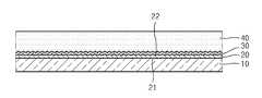
- FIG. 1is a cross-sectional diagram of a printed circuit board (PCB) according to an embodiment of the present invention
- FIG. 2is a cross-sectional diagram of a PCB according to another embodiment of the present invention.
- FIGS. 3 and 4are cross-sectional diagrams illustrating a method of manufacturing a PCB according to another embodiment of the present invention.
- FIG. 5is a cross-sectional diagram of a PCB according to another embodiment of the present invention.
- FIG. 6is a cross-sectional diagram of a PCB according to another embodiment of the present invention.
- FIG. 7is a scanning electron microscope (SEM) photograph of a second surface.
- FIG. 1is a cross-sectional diagram of a printed circuit board (PCB) according to an embodiment of the present invention.
- the PCBincludes a first metal film 10 , a second metal film 20 , and a polymer film 40 .
- the first metal film 10is formed of copper or a copper alloy and corresponds to a conductive layer, on which a circuit pattern is formed.
- the polymer film 40formed of polyimide or acrylic resin, is formed to face the first metal film 10 .
- the second metal film 20is interposed between the first metal film 10 and the polymer film 40 and is formed of nickel or a nickel alloy.
- the second metal film 20includes a first surface 21 facing the first metal film 10 and a second surface 22 facing the polymer film 40 .
- the second metal film 20may be formed on the first metal film 10 using electroplating.
- the surface of the second surface 22may be rougher than the surface of the first surface 21 .
- the polymer film 40is formed on the second surface 22 of the second metal film 20 so as to cover the second surface 22 .
- the second surface 22 contacting the polymer film 40is rough, adhesion between the polymer film 40 and the second metal film 20 is improved.
- the second metal film 20closely adheres to the first metal film 10 due to the electroplating so that adhesion between the first metal film 10 and the polymer film 40 may be improved by the second metal film 20 .
- the adhesion between the polymer film 40 and the first metal film 10may be simply improved.
- the PCB described aboveis manufactured as follows.
- the first metal film 10 formed of copper or a copper alloyis prepared.
- the second metal film 20is formed on one side of the first metal film 10 , that is, the upper surface of the metal thin film 10 as viewed in FIG. 1 , by using electroplating.
- the second metal film 20is formed to be a rough plating layer.
- the second surface 22 formed opposite to the first surface 21 contacting the first metal film 10is electroplated to be rough.
- the second metal film 20may be formed of nickel or a nickel alloy.
- the composition of a nickel plating bath for forming a rough plating layer as in the second metal film 20may include 2.5-3.5 g/l of nickel sulfate or nickel chloride, 2.5-3.0 g/l of ammonium sulfate, 4.5-5.0 g/l of sodium sulfate, 1.5-2.0 g/l of sodium chloride, and 2.0-3.0 g/l of boric acid.
- nickel sulfate or nickel chloridemay have a low concentration of 10% or less of the composition of the plating bath for forming a general nickel plating layer.
- a high current density of 10 ASD (A/dm 2 ) or greateris applied to the plating bath with the composition described above so that the second metal film 20 , which is a nickel plating layer having a rough surface, is formed.
- the plating processmay be a reel-to-reel type which provides the first metal film 10 , rolled to one side of a roller, to the plating bath, the first metal film 10 being rolled to the other side of the roller after plating is completed.
- a high current density of 50 ASDmay be applied.
- a plating process timemay take 3-20 seconds. During a plating process time of 3 seconds or below, growth of nickel crystal does not occur. When the plating process time is 20 seconds or greater, secondary contamination such as smut may occur on the rough nickel plating layer due to excessive growth of nickel crystal.
- the second metal film 20 formed of the rough nickel plating layermay have a thickness of 0.1-0.5 ⁇ m.
- efficiency of the rough plating layermay be low and when the second metal film 20 has a thickness of 0.5 ⁇ m or greater, the plating layer may be exfoliated due to excessive growth of nickel plating. That is, growth of nickel in a vertical direction is insignificant in a plating layer having a thickness of 0.1 ⁇ m or below and the plating layer having a thickness of 0.5 ⁇ m or greater may be separated due to excessive growth in a vertical direction.
- FIG. 7is a scanning electron microscope (SEM) photograph of the second surface 22 of the second metal film 20 included in the PCB according to an embodiment of the present invention.
- SEMscanning electron microscope
- the second metal film 20After the second metal film 20 is manufactured, whether the second surface 22 has a desired surface roughness may be examined by a scanning electron microscope (SEM). However, time for the examination is needed, and thus, methods of rapidly identifying surface roughness during the process are needed.
- SEMscanning electron microscope
- gloss testingmay be used. That is, when the gloss of the second surface 22 is in the range of about 0.2 to 0.8, it is regarded that the second metal film 20 having a desired surface roughness is manufactured. In a gloss of 0.2 or below, roughness is excessively achieved so that the polymer resin forming the polymer film 40 may run over during the forming of the polymer film 40 and a secondary quality problem such as resin bleed overflow (RBO) may be generated. In gloss of 0.8 or greater, roughness is not sufficiently achieved and thus a moisture sensitivity level (MSL) is not improved.
- RBOresin bleed overflow
- a precursor of a polyimide monomeris cast on the second surface 22 of the second metal film 20 and then, the polymer film 40 formed of polyimide may be formed by cross-linking at a high temperature.
- a seed layersuch as nickel or chrome is formed on a polyimide film using sputtering and then is copper plated, thereby forming a copper foil.
- the second metal film 20 having a rough surfaceis firstly formed on the copper foil, that is, the first metal film 10 by electroplating and then, the polymer film 40 is formed on the second metal film 20 as described above.
- the adhesion between the metal thin film 10 and the polymer film 40may be improved, and productivity and manufacturing costs may be improved due to a simplified manufacturing process.
- the second metal film 20 and the polymer film 40are sequentially formed on both surfaces of the first metal film 10 using the process described above so that the PCB may be formed using films in which the outer surfaces are insulated.
- FIGS. 3 and 4are cross-sectional diagrams illustrating a method of manufacturing a PCB according to another embodiment of the present invention.
- second metal films 20 and 20 ′are respectively formed on the surfaces of first metal film 10 and 10 ′ by using rough plating and then, second surfaces 22 and 22 ′ of the second metal films 20 and 20 ′ are disposed to face each other.
- a precursor of a polyimide monomeris cast between the second surfaces 22 and 22 ′, which face each other, and the polymer film 40 formed of polyimide is formed by cross-linking at a high temperature.
- the first metal films 10 and 10 ′ for forming a circuit patternmay be disposed on both sides of the polymer film 40 .
- the second metal films 20 and 20 ′are respectively plated on both sides of the first metal films 10 and 10 ′ and then the polymer film 40 is formed on the second metal films 20 and 20 ′ as in FIG. 2 .
- the first metal films 10 and 10 ′ for forming a circuit patternare disposed on both sides of the polymer film 40 and then the polymer films 40 may be formed to cover the outer surfaces of the first metal films 10 and 10 ′, thereby manufacturing a multi-layered PCB.
- FIG. 6is a cross-sectional diagram of a PCB according to another embodiment of the present invention.
- the second metal film 20is formed on one surface of the first metal film 10 using rough plating as in FIG. 1 and then, a third metal film 30 is formed on the second surface 22 of the second metal film 20 . Then, the polymer film 40 is formed on the third metal film 30 .
- the third metal film 30may be formed of nickel (Ni), palladium (Pd), gold (Au), or an alloy thereof and may function as a diffusion preventing layer for preventing a metal component of the first metal film 10 from being diffused in the polymer film 40 during forming of the polymer film 40 , that is, for preventing the metal component of the first metal film 10 from being diffused in the interface between the polymer film 40 and the second metal film 20 and thereby, preventing adhesion between the polymer film 40 and the second metal film 20 from deteriorating.
- the third metal film 30is interposed between the polymer film 40 and the second metal film 20 , a metal component of the first metal film 10 is prevented from being diffused so that reliability and adhesion at a high-temperature and in a hygroscopic environment may be improved.
- the third metal film 30is not formed by the rough plating as in the second metal film 20 .
- the third metal film 30may be formed using a conventional plating process. Accordingly, a plating bath with a higher density than that of the plating bath for forming the second metal film 20 is used to form the third metal film 30 and the third metal film 30 is plated at a low current density.
- the third metal film 30is formed on the second surface 22 having the rough surface, the third metal film 30 may be formed to be thin so that roughness of the second surface 22 is applied to the third metal film 30 .
- the third metal film 30may have a thickness of 0.1-0.5 ⁇ m. When the third metal film 30 has a thickness of 0.1 ⁇ m or below, the third metal film 30 may not function as a diffusion preventing layer. When the third metal film 30 has a thickness of 0.5 ⁇ m or greater, the rough surface is not formed on the third metal film 30 , thereby decreasing the adhesion between the third metal film 30 and the polymer film 40 .
- the third metal film 30may be formed as a single layer. However, the present invention is not limited thereto and the third metal film 30 may be formed as multiple layers.
- the third metal film 30may be also formed in the PCB illustrated in FIGS. 2-5 .
- a first metal film formed of a copper alloyis prepared.
- a current density of 20 ASDflows in a plating bath including 3.5 g/l of nickel sulfate, 2.75 g/l of ammonium sulfate, 4.75 g/l of sodium sulfate, 1.75 g/l of sodium chloride, and 2.5 g/l of boric acid, and the first metal film is filled in the plating bath so as to be plated for 20 seconds.
- a second surface of a second metal film formed in the plating bathis rough enough that adhesion between the second surface and a polymer film may be improved.
- a precursor of a polyimide monomeris cast on the second surface of the second metal film and then, is cross-linked at a temperature of 450° C., thereby forming the polymer film.
- hard PCBs and soft PCBs used in various electric, mechanical, and electronic equipmentsmay be manufactured. More specifically, the method of manufacturing the PCB according to the present invention may be useful in manufacturing casting type flexible copper clad laminates (FCCL), in which fine pitch patterned circuits are formed by etching.
- FCCLflexible copper clad laminates
Landscapes
- Chemical & Material Sciences (AREA)
- Engineering & Computer Science (AREA)
- Metallurgy (AREA)
- Chemical Kinetics & Catalysis (AREA)
- Electrochemistry (AREA)
- Materials Engineering (AREA)
- Organic Chemistry (AREA)
- Microelectronics & Electronic Packaging (AREA)
- Manufacturing & Machinery (AREA)
- Manufacturing Of Printed Wiring (AREA)
- Laminated Bodies (AREA)
- Electroplating Methods And Accessories (AREA)
- Parts Printed On Printed Circuit Boards (AREA)
Abstract
Description
Claims (9)
Applications Claiming Priority (2)
| Application Number | Priority Date | Filing Date | Title |
|---|---|---|---|
| KR1020080112865AKR101426038B1 (en) | 2008-11-13 | 2008-11-13 | Printed circuit board and method of manufacturing the same |
| KR10-2008-0112865 | 2008-11-13 |
Publications (2)
| Publication Number | Publication Date |
|---|---|
| US20100116528A1 US20100116528A1 (en) | 2010-05-13 |
| US8409726B2true US8409726B2 (en) | 2013-04-02 |
Family
ID=42164147
Family Applications (1)
| Application Number | Title | Priority Date | Filing Date |
|---|---|---|---|
| US12/475,764Active2030-12-03US8409726B2 (en) | 2008-11-13 | 2009-06-01 | Printed circuit board with multiple metallic layers and method of manufacturing the same |
Country Status (3)
| Country | Link |
|---|---|
| US (1) | US8409726B2 (en) |
| JP (1) | JP5474500B2 (en) |
| KR (1) | KR101426038B1 (en) |
Cited By (3)
| Publication number | Priority date | Publication date | Assignee | Title |
|---|---|---|---|---|
| US10586748B2 (en) | 2016-04-22 | 2020-03-10 | Samsung Electronics Co., Ltd. | Printed circuit board and semiconductor package |
| US20230300983A1 (en)* | 2020-07-29 | 2023-09-21 | Kyocera Corporation | Circuit substrate and method for manufacturing the same |
| US12446153B2 (en)* | 2020-07-29 | 2025-10-14 | Kyocera Corporation | Circuit substrate and method for manufacturing the same |
Families Citing this family (14)
| Publication number | Priority date | Publication date | Assignee | Title |
|---|---|---|---|---|
| KR101871029B1 (en)* | 2010-09-27 | 2018-06-25 | 제이엑스금속주식회사 | Copper foil for printed wiring board, method for producing said copper foil, resin substrate for printed wiring board, and printed wiring board |
| US9674955B2 (en) | 2011-11-09 | 2017-06-06 | Lg Innotek Co., Ltd. | Tape carrier package, method of manufacturing the same and chip package |
| CN103635009A (en)* | 2012-08-28 | 2014-03-12 | 昆山雅森电子材料科技有限公司 | Yellow polyamidoimide protection film for printed circuit board and manufacturing method thereof |
| CN103813616A (en)* | 2012-11-13 | 2014-05-21 | 昆山雅森电子材料科技有限公司 | Composite stackup covering film, circuit board provided with covering film and manufacturing method thereof |
| JP6310192B2 (en)* | 2013-07-02 | 2018-04-11 | Jx金属株式会社 | Copper foil with carrier and method for producing the same, method for producing copper-clad laminate and method for producing printed wiring board |
| JP6310191B2 (en)* | 2013-07-02 | 2018-04-11 | Jx金属株式会社 | Copper foil with carrier and method for producing the same, method for producing copper-clad laminate and method for producing printed wiring board |
| JP6310193B2 (en)* | 2013-07-02 | 2018-04-11 | Jx金属株式会社 | Copper foil with carrier, method for producing the same, method for producing copper-clad laminate, and method for producing printed wiring board |
| CN105247111B (en) | 2013-10-25 | 2017-09-12 | Om产业股份有限公司 | Manufacturing method of plating products |
| DE102014210483A1 (en)* | 2014-06-03 | 2015-12-03 | Conti Temic Microelectronic Gmbh | Method for producing a foil arrangement and corresponding foil arrangement |
| US20170334170A1 (en)* | 2016-03-23 | 2017-11-23 | Atieh Haghdoost | Articles including adhesion enhancing coatings and methods of producing them |
| CN111405980A (en) | 2017-09-28 | 2020-07-10 | 麦克斯特里尔有限公司 | Article including surface coating and method for producing the same |
| CN110996546A (en)* | 2019-12-31 | 2020-04-10 | 华宇华源电子科技(深圳)有限公司 | Method for enhancing surface pressure resistance of PCB (printed circuit board) |
| KR102844898B1 (en)* | 2020-04-27 | 2025-08-11 | 엘지이노텍 주식회사 | Circuit board, driving apparatus of image sensor, and camera module including the same |
| CA3224559A1 (en) | 2021-06-18 | 2022-12-22 | Maxterial, Inc. | Moveable components with surface coatings |
Citations (24)
| Publication number | Priority date | Publication date | Assignee | Title |
|---|---|---|---|---|
| US3884771A (en)* | 1972-06-29 | 1975-05-20 | Fujitsu Ltd | Process of producing resinous board having a rough surface usable for firmly supporting thereon a printed circuit |
| US4049481A (en)* | 1975-12-17 | 1977-09-20 | Mitsui-Anaconda Electro Copper Sheet Co. Ltd. | Surface treatment method of copperfoil |
| US4101402A (en)* | 1975-07-25 | 1978-07-18 | Rca Corporation | Adherence of metal films to polymeric materials |
| US4640747A (en)* | 1984-11-06 | 1987-02-03 | Mitsui Mining And Smelting Co., Ltd. | Process for surface treatment of copper product |
| US4935310A (en)* | 1980-04-03 | 1990-06-19 | Furukawa Circuit Foil Co., Ltd. | Copper foil for a printed circuit and a method for the production thereof |
| US5242861A (en)* | 1991-06-06 | 1993-09-07 | Nec Corporation | Method for manufacturing semiconductor device having a multilayer wiring structure |
| US5243320A (en)* | 1988-02-26 | 1993-09-07 | Gould Inc. | Resistive metal layers and method for making same |
| US5403672A (en)* | 1992-08-17 | 1995-04-04 | Hitachi Chemical Co., Ltd. | Metal foil for printed wiring board and production thereof |
| US5767008A (en)* | 1995-02-20 | 1998-06-16 | Matsushita Electric Industrial Co., Ltd. | Method for forming a gold plating electrode, a substrate based on the electrode forming method, and a wire bonding method utilizing this electrode forming method |
| US5800930A (en)* | 1994-01-21 | 1998-09-01 | Olin Corporation | Nodular copper/nickel alloy treatment for copper foil |
| US6171714B1 (en)* | 1996-04-18 | 2001-01-09 | Gould Electronics Inc. | Adhesiveless flexible laminate and process for making adhesiveless flexible laminate |
| US6359233B1 (en)* | 1999-10-26 | 2002-03-19 | Intel Corporation | Printed circuit board multipack structure having internal gold fingers and multipack and printed circuit board formed therefrom, and methods of manufacture thereof |
| US6497806B1 (en)* | 2000-04-25 | 2002-12-24 | Nippon Denkai, Ltd. | Method of producing a roughening-treated copper foil |
| KR20030039937A (en) | 2001-11-16 | 2003-05-22 | 엘지전선 주식회사 | The surface treatment of electrodeposited copper foil for Printed Circuit Board |
| US6771160B2 (en)* | 2000-09-22 | 2004-08-03 | Nikko Materials Usa, Inc. | Resistor component with multiple layers of resistive material |
| US6939622B2 (en)* | 2003-02-17 | 2005-09-06 | Furukawa Circuit Foil Co., Ltd | Chip-on-film use copper foil |
| JP2005353918A (en) | 2004-06-11 | 2005-12-22 | Hitachi Cable Ltd | Copper foil for printed wiring board and method for producing the same |
| US6989199B2 (en)* | 2001-08-06 | 2006-01-24 | Mitsui Mining & Smelting Co., Ltd. | Copper foil for printed-wiring board and copper-clad laminate using copper foil for printed-wiring board |
| US6994918B2 (en)* | 2003-08-12 | 2006-02-07 | Johnson Morgan T | Selective application of conductive material to circuit boards by pick and place |
| US7026059B2 (en)* | 2000-09-22 | 2006-04-11 | Circuit Foil Japan Co., Ltd. | Copper foil for high-density ultrafine printed wiring boad |
| US7108923B1 (en)* | 2005-05-16 | 2006-09-19 | Hitachi Cable, Ltd. | Copper foil for printed circuit board with taking environmental conservation into consideration |
| KR20060109122A (en) | 2005-04-15 | 2006-10-19 | 삼성테크윈 주식회사 | Lead Frames for Semiconductor Packages |
| US7223481B2 (en)* | 2003-09-01 | 2007-05-29 | Furukawa Circuit Foil Co., Inc. | Method of producing ultra-thin copper foil with carrier, ultra-thin copper foil with carrier produced by the same, printed circuit board, multilayer printed circuit board and chip on film circuit board |
| US7691487B2 (en)* | 2002-07-04 | 2010-04-06 | Mitsui Mining & Smelting Co., Ltd. | Electrodeposited copper foil with carrier foil |
Family Cites Families (1)
| Publication number | Priority date | Publication date | Assignee | Title |
|---|---|---|---|---|
| US8449987B2 (en)* | 2006-06-12 | 2013-05-28 | Jx Nippon Mining & Metals Corporation | Rolled copper or copper alloy foil with roughened surface and method of roughening rolled copper or copper alloy foil |
- 2008
- 2008-11-13KRKR1020080112865Apatent/KR101426038B1/enactiveActive
- 2009
- 2009-06-01USUS12/475,764patent/US8409726B2/enactiveActive
- 2009-11-12JPJP2009258564Apatent/JP5474500B2/enactiveActive
Patent Citations (25)
| Publication number | Priority date | Publication date | Assignee | Title |
|---|---|---|---|---|
| US3884771A (en)* | 1972-06-29 | 1975-05-20 | Fujitsu Ltd | Process of producing resinous board having a rough surface usable for firmly supporting thereon a printed circuit |
| US4101402A (en)* | 1975-07-25 | 1978-07-18 | Rca Corporation | Adherence of metal films to polymeric materials |
| US4049481A (en)* | 1975-12-17 | 1977-09-20 | Mitsui-Anaconda Electro Copper Sheet Co. Ltd. | Surface treatment method of copperfoil |
| US4935310A (en)* | 1980-04-03 | 1990-06-19 | Furukawa Circuit Foil Co., Ltd. | Copper foil for a printed circuit and a method for the production thereof |
| US4640747A (en)* | 1984-11-06 | 1987-02-03 | Mitsui Mining And Smelting Co., Ltd. | Process for surface treatment of copper product |
| US5243320A (en)* | 1988-02-26 | 1993-09-07 | Gould Inc. | Resistive metal layers and method for making same |
| US5242861A (en)* | 1991-06-06 | 1993-09-07 | Nec Corporation | Method for manufacturing semiconductor device having a multilayer wiring structure |
| US5403672A (en)* | 1992-08-17 | 1995-04-04 | Hitachi Chemical Co., Ltd. | Metal foil for printed wiring board and production thereof |
| US5800930A (en)* | 1994-01-21 | 1998-09-01 | Olin Corporation | Nodular copper/nickel alloy treatment for copper foil |
| US5767008A (en)* | 1995-02-20 | 1998-06-16 | Matsushita Electric Industrial Co., Ltd. | Method for forming a gold plating electrode, a substrate based on the electrode forming method, and a wire bonding method utilizing this electrode forming method |
| US6331347B2 (en)* | 1995-02-20 | 2001-12-18 | Matsushita Electric Industrial Co., Ltd | Method for forming a gold plating electrode a substrate based on the electrode forming method, and a wire bonding method utilizing this electrode forming method |
| US6171714B1 (en)* | 1996-04-18 | 2001-01-09 | Gould Electronics Inc. | Adhesiveless flexible laminate and process for making adhesiveless flexible laminate |
| US6359233B1 (en)* | 1999-10-26 | 2002-03-19 | Intel Corporation | Printed circuit board multipack structure having internal gold fingers and multipack and printed circuit board formed therefrom, and methods of manufacture thereof |
| US6497806B1 (en)* | 2000-04-25 | 2002-12-24 | Nippon Denkai, Ltd. | Method of producing a roughening-treated copper foil |
| US6771160B2 (en)* | 2000-09-22 | 2004-08-03 | Nikko Materials Usa, Inc. | Resistor component with multiple layers of resistive material |
| US7026059B2 (en)* | 2000-09-22 | 2006-04-11 | Circuit Foil Japan Co., Ltd. | Copper foil for high-density ultrafine printed wiring boad |
| US6989199B2 (en)* | 2001-08-06 | 2006-01-24 | Mitsui Mining & Smelting Co., Ltd. | Copper foil for printed-wiring board and copper-clad laminate using copper foil for printed-wiring board |
| KR20030039937A (en) | 2001-11-16 | 2003-05-22 | 엘지전선 주식회사 | The surface treatment of electrodeposited copper foil for Printed Circuit Board |
| US7691487B2 (en)* | 2002-07-04 | 2010-04-06 | Mitsui Mining & Smelting Co., Ltd. | Electrodeposited copper foil with carrier foil |
| US6939622B2 (en)* | 2003-02-17 | 2005-09-06 | Furukawa Circuit Foil Co., Ltd | Chip-on-film use copper foil |
| US6994918B2 (en)* | 2003-08-12 | 2006-02-07 | Johnson Morgan T | Selective application of conductive material to circuit boards by pick and place |
| US7223481B2 (en)* | 2003-09-01 | 2007-05-29 | Furukawa Circuit Foil Co., Inc. | Method of producing ultra-thin copper foil with carrier, ultra-thin copper foil with carrier produced by the same, printed circuit board, multilayer printed circuit board and chip on film circuit board |
| JP2005353918A (en) | 2004-06-11 | 2005-12-22 | Hitachi Cable Ltd | Copper foil for printed wiring board and method for producing the same |
| KR20060109122A (en) | 2005-04-15 | 2006-10-19 | 삼성테크윈 주식회사 | Lead Frames for Semiconductor Packages |
| US7108923B1 (en)* | 2005-05-16 | 2006-09-19 | Hitachi Cable, Ltd. | Copper foil for printed circuit board with taking environmental conservation into consideration |
Non-Patent Citations (1)
| Title |
|---|
| Search Report established for JP 2009-258564 (Jul. 3, 2012). |
Cited By (4)
| Publication number | Priority date | Publication date | Assignee | Title |
|---|---|---|---|---|
| US10586748B2 (en) | 2016-04-22 | 2020-03-10 | Samsung Electronics Co., Ltd. | Printed circuit board and semiconductor package |
| US10950517B2 (en) | 2016-04-22 | 2021-03-16 | Samsung Electronics Co., Ltd. | Printed circuit board and semiconductor package |
| US20230300983A1 (en)* | 2020-07-29 | 2023-09-21 | Kyocera Corporation | Circuit substrate and method for manufacturing the same |
| US12446153B2 (en)* | 2020-07-29 | 2025-10-14 | Kyocera Corporation | Circuit substrate and method for manufacturing the same |
Also Published As
| Publication number | Publication date |
|---|---|
| KR101426038B1 (en) | 2014-08-01 |
| KR20100053964A (en) | 2010-05-24 |
| JP5474500B2 (en) | 2014-04-16 |
| JP2010118662A (en) | 2010-05-27 |
| US20100116528A1 (en) | 2010-05-13 |
Similar Documents
| Publication | Publication Date | Title |
|---|---|---|
| US8409726B2 (en) | Printed circuit board with multiple metallic layers and method of manufacturing the same | |
| US20180279482A1 (en) | Surface-treated copper foil, copper foil with carrier, substrate, resin substrate, printed wiring board, copper clad laminate and method for producing printed wiring board | |
| US7691487B2 (en) | Electrodeposited copper foil with carrier foil | |
| JP5178064B2 (en) | Metal layer laminate having metal surface roughened layer and method for producing the same | |
| US20120111613A1 (en) | Copper foil with resistance layer, method of production of the same and laminated board | |
| TWI504323B (en) | Adhesiveless copper clad laminates and printed circuit board having adhesiveless copper clad laminates as base material | |
| KR101256086B1 (en) | Metal foil, method for producing same, insulating substrate, and wiring board | |
| JP5248684B2 (en) | Electronic circuit, method for forming the same, and copper-clad laminate for forming electronic circuit | |
| US8357307B2 (en) | Method of forming electronic circuit | |
| TW202001000A (en) | Surface-treated copper foil, copper-cladded laminate plate, and printed wiring board | |
| JP3250994B2 (en) | Electrolytic copper foil | |
| WO2020246467A1 (en) | Surface-treated copper foil, copper-clad laminate plate, and printed wiring board | |
| US20110091739A1 (en) | Composite material for electrical/electronic part and electrical/electronic part using the same | |
| JPWO2010147059A1 (en) | Electronic circuit, method for forming the same, and copper-clad laminate for forming electronic circuit | |
| JP4294363B2 (en) | Two-layer flexible copper-clad laminate and method for producing the two-layer flexible copper-clad laminate | |
| TWI805902B (en) | Surface treated copper foil, copper clad laminate and printed circuit board | |
| JP2008085009A (en) | Circuit board, and electronic equipment | |
| KR20140072409A (en) | Method for processing a flexible cupper clad laminated film | |
| TW201247041A (en) | Method for forming electronic circuit, electronic circuit, and copper-clad laminated board for forming electronic circuit | |
| JP4872257B2 (en) | Two-layer plated substrate and manufacturing method thereof | |
| TWI808777B (en) | Coarse treatment of copper foil, copper foil laminates and printed wiring boards | |
| KR102504286B1 (en) | Surface treated copper foil and Method for producing the same | |
| KR100727715B1 (en) | Flexible Metal Laminates, Manufacturing Method, Plating Apparatus and Plating Method | |
| JPH09115961A (en) | Method for manufacturing electronic circuit component material using copper-coated polyimide substrate | |
| JP2008091596A (en) | Copper-coated polyimide substrate having surface smoothness and manufacturing method thereof |
Legal Events
| Date | Code | Title | Description |
|---|---|---|---|
| AS | Assignment | Owner name:SAMSUNG TECHWIN CO., LTD.,KOREA, REPUBLIC OF Free format text:ASSIGNMENT OF ASSIGNORS INTEREST;ASSIGNORS:SHIM, CHANG-HAN;KANG, SUNG-IL;PARK, SE-CHUEL;REEL/FRAME:022842/0668 Effective date:20090326 Owner name:SAMSUNG TECHWIN CO., LTD., KOREA, REPUBLIC OF Free format text:ASSIGNMENT OF ASSIGNORS INTEREST;ASSIGNORS:SHIM, CHANG-HAN;KANG, SUNG-IL;PARK, SE-CHUEL;REEL/FRAME:022842/0668 Effective date:20090326 | |
| FEPP | Fee payment procedure | Free format text:PAYOR NUMBER ASSIGNED (ORIGINAL EVENT CODE: ASPN); ENTITY STATUS OF PATENT OWNER: LARGE ENTITY | |
| STCF | Information on status: patent grant | Free format text:PATENTED CASE | |
| AS | Assignment | Owner name:MDS CO., LTD., KOREA, REPUBLIC OF Free format text:ASSIGNMENT OF ASSIGNORS INTEREST;ASSIGNOR:SAMSUNG TECHWIN CO., LTD.;REEL/FRAME:032880/0089 Effective date:20140430 | |
| AS | Assignment | Owner name:HAESUNG DS CO., LTD., KOREA, REPUBLIC OF Free format text:CHANGE OF NAME;ASSIGNOR:MDS CO., LTD.;REEL/FRAME:035447/0366 Effective date:20140901 | |
| FPAY | Fee payment | Year of fee payment:4 | |
| MAFP | Maintenance fee payment | Free format text:PAYMENT OF MAINTENANCE FEE, 8TH YEAR, LARGE ENTITY (ORIGINAL EVENT CODE: M1552); ENTITY STATUS OF PATENT OWNER: LARGE ENTITY Year of fee payment:8 | |
| MAFP | Maintenance fee payment | Free format text:PAYMENT OF MAINTENANCE FEE, 12TH YEAR, LARGE ENTITY (ORIGINAL EVENT CODE: M1553); ENTITY STATUS OF PATENT OWNER: LARGE ENTITY Year of fee payment:12 |