US8407478B2 - Control message signature for device control - Google Patents
Control message signature for device controlDownload PDFInfo
- Publication number
- US8407478B2 US8407478B2US12/498,381US49838109AUS8407478B2US 8407478 B2US8407478 B2US 8407478B2US 49838109 AUS49838109 AUS 49838109AUS 8407478 B2US8407478 B2US 8407478B2
- Authority
- US
- United States
- Prior art keywords
- signature
- peripheral device
- control message
- address
- system memory
- Prior art date
- Legal status (The legal status is an assumption and is not a legal conclusion. Google has not performed a legal analysis and makes no representation as to the accuracy of the status listed.)
- Active, expires
Links
- 230000002093peripheral effectEffects0.000claimsabstractdescription72
- 238000000034methodMethods0.000claimsabstractdescription26
- 230000005540biological transmissionEffects0.000claimsabstractdescription9
- 238000012545processingMethods0.000claimsdescription24
- 238000004590computer programMethods0.000claimsdescription12
- 238000010586diagramMethods0.000description9
- 230000006870functionEffects0.000description8
- 238000010200validation analysisMethods0.000description5
- 238000012986modificationMethods0.000description4
- 230000004048modificationEffects0.000description4
- 238000004891communicationMethods0.000description3
- 230000009471actionEffects0.000description2
- 125000004122cyclic groupChemical group0.000description2
- 239000000463materialSubstances0.000description2
- 230000003287optical effectEffects0.000description2
- 239000013307optical fiberSubstances0.000description2
- 230000008859changeEffects0.000description1
- 230000000644propagated effectEffects0.000description1
- 239000004065semiconductorSubstances0.000description1
- 230000003068static effectEffects0.000description1
- 238000012546transferMethods0.000description1
Images


Classifications
- H—ELECTRICITY
- H04—ELECTRIC COMMUNICATION TECHNIQUE
- H04L—TRANSMISSION OF DIGITAL INFORMATION, e.g. TELEGRAPHIC COMMUNICATION
- H04L9/00—Cryptographic mechanisms or cryptographic arrangements for secret or secure communications; Network security protocols
- H04L9/32—Cryptographic mechanisms or cryptographic arrangements for secret or secure communications; Network security protocols including means for verifying the identity or authority of a user of the system or for message authentication, e.g. authorization, entity authentication, data integrity or data verification, non-repudiation, key authentication or verification of credentials
- H04L9/3247—Cryptographic mechanisms or cryptographic arrangements for secret or secure communications; Network security protocols including means for verifying the identity or authority of a user of the system or for message authentication, e.g. authorization, entity authentication, data integrity or data verification, non-repudiation, key authentication or verification of credentials involving digital signatures
- H—ELECTRICITY
- H04—ELECTRIC COMMUNICATION TECHNIQUE
- H04L—TRANSMISSION OF DIGITAL INFORMATION, e.g. TELEGRAPHIC COMMUNICATION
- H04L2209/00—Additional information or applications relating to cryptographic mechanisms or cryptographic arrangements for secret or secure communication H04L9/00
- H04L2209/80—Wireless
Definitions
- the present inventionrelates generally to the field of computer peripheral devices and more particularly relates to controlling a computer peripheral device.
- Error checking codesare a common technique for detecting accidental changes to computer data, and are used in many modern digital networks and storage devices.
- an error checking codecomprises a fixed-size data element computed from a block of digital data for the purpose of detecting accidental errors that may have been introduced during transmission or storage. The integrity of the block of digital data can be checked at any later time by recomputing the error checking code and comparing it with the stored one. If the codes do not match, then the block of digital data contains a data error.
- error checking codesinclude, without limitation, checksums and cyclic redundancy checks (CRC).
- CRCcyclic redundancy checks
- a method of controlling a peripheral deviceincluding generating, in a host processor, a control message for transmission to the peripheral device, calculating a signature for the control message, writing the control message and the signature to an address in a system memory of the host processor, and notifying the peripheral device of the address, so as to cause the device to read the control message and the signature.
- a method of controlling a peripheral deviceincluding receiving in the peripheral device a notification from a host processor of an address to which a control message for the peripheral device has been written together with a signature in a system memory of the host processor, reading into the peripheral device the control message and the signature from the address in the system memory, verifying the signature, and upon successfully verifying the signature, executing the control message in the peripheral device.
- a method of controlling a peripheral deviceincluding generating, in a host processor, a control message for transmission to the peripheral device, calculating a signature for the control message, writing the control message and the signature to an address in a system memory of the host processor, notifying the peripheral device of the address, so as to cause the device to read the control message and the signature, receiving in the peripheral device the notification from the host processor of the address to which the control message for the peripheral device has been written together with the signature in the system memory of the host processor, reading into the peripheral device a control message and the signature from the address in the system memory, verifying the signature, and upon successfully verifying the signature, executing the control message in the peripheral device.
- a computer program productfor controlling a peripheral device
- the computer program productincluding a computer usable medium having computer usable code embodied therewith, the computer usable program code including computer usable code configured for generating, in a host processor, a control message for transmission to the peripheral device, computer usable code configured for calculating a signature for the control message, computer usable code configured for writing the control message and the signature to an address in a system memory of the host processor, and computer usable code configured for notifying the peripheral device of the address, so as to cause the device to read the control message and the signature.
- a computer peripheral deviceincluding a host interface, which is coupled to communicate with a host processor and a system memory of the host processor and a processing circuit which is configured to receive a notification from the host processor of an address to which a control message for the peripheral device has been written together with a signature in the system memory, to read the control message and the signature from the address in the system memory, to verify the signature, and upon successfully verifying the signature, to execute the control message.
- FIG. 1is a diagram schematically illustrating an example computer processing system implementing a technique for device control message integrity, in accordance with an embodiment of the present invention
- FIG. 2is a diagram that schematically shows details of an example network interface adapter processing a device control message in accordance with an embodiment of the present invention
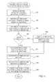
- FIG. 3is a flow diagram illustrating a protected command register load method, in accordance with an embodiment of the present invention.
- FIG. 4is a flow diagram illustrating a protected command register read method, in accordance with an embodiment of the present invention.
- a host processorcontrols a device (typically, but not limited to a computer peripheral device) by writing a control message the device.
- the control messagetypically has the form of a numerical value that is loaded directly by the host processor into a register on the device.
- the deviceUpon detecting a numerical value written to one of its registers, the device changes its status and executes the control message corresponding to the numerical value written to the register.
- a potential danger with allowing a control message to be written to a device register in this manneris that an unintended or incorrect write to a device register can result in a change in the device status.
- These problemscan arise from a bug in a computer program, which causes the host processor to perform an incorrect (with respect to the program specifications) write to a device register.
- the devicemay attempt to execute an unintended (and potentially invalid or harmful) control message, which may affect overall system stability and reliability, potentially leading to either a system level error or silent data corruption.
- a host processorcontrols a device by writing the control message to a certain address in system memory (referred to as a “mailbox”) and then notifying the device of the address by loading the address into a mailbox address register in the device. Once the device detects the address in the mailbox address register, the device executes the control message by reading the memory address, retrieving the control message and then executing the necessary operation(s).
- the host processoris only allowed to write to the mailbox address register. Communication with other registers in the device is effected by writing a control message to a mailbox in system memory and loading the mailbox address to the mailbox address register.
- Potential problems with writing a control message to a mailboxinclude (1) an incorrect address loaded into the device mailbox register and (2) an invalid command message stored in system memory.
- An embodiment of the present inventionaddresses these potential problems by having the host processor append a signature comprising an error checking code to the control message that the host processor writes to the mailbox in system memory.
- the deviceUpon receiving notification of the address from the host processor, the device retrieves the control message and the signature from the mailbox. The device verifies the signature and then executes the control message only if the signature is valid. This ensures that only intended and valid control messages are acted upon by the device.
- the present inventionmay be embodied as a system, method, computer program product or any combination thereof. Accordingly, the present invention may take the form of an entirely hardware embodiment, an entirely software embodiment (including firmware, resident software, micro-code, etc.) or an embodiment combining software and hardware aspects that may all generally be referred to herein as a “circuit,” “module” or “system.” Furthermore, the present invention may take the form of a computer program product embodied in any tangible medium of expression having computer usable program code embodied in the medium.
- the computer-usable or computer-readable mediummay be, for example but not limited to, a tangible storage medium, such an electronic, magnetic or optical memory device.
- the mediummay comprise an electromagnetic, infrared, or semiconductor system, apparatus, device, or propagation medium.
- a computer-usable or computer-readable mediummay be any medium that can contain, store, communicate, propagate, or transport the program for use by or in connection with the instruction execution system, apparatus, or device.
- the computer-usable mediummay include a propagated data signal with the computer-usable program code embodied therewith, either in baseband or as part of a carrier wave.
- the computer usable program codemay be transmitted using any appropriate medium, including but not limited to wireless, wireline, optical fiber cable, RF, etc.
- FIG. 1is a schematic pictorial illustration of an example computer system 10 , in accordance with an embodiment of the present invention.
- System 10comprises a central processing unit (CPU) 12 , which is programmed in software to carry out the functions that are described hereinbelow.
- the systemalso comprises a system memory 14 , which may comprise both static read only memory and a dynamic main memory, in communication with the processor.
- the computer systemis connected to one or more external networks 18 , such as a LAN or WAN, by communication lines connected to the system via a data I/O device 16 , identified here as a network interface device (or network interface card—NIC).
- Data I/O device 16enables system 10 to become coupled to other data processing systems or remote printers or storage devices through intervening private or public networks.
- device 16may comprise an InfiniBandTM host channel adapter (HCA).
- HCAInfiniBandTM host channel adapter
- I/O device 16is shown and described here only by way of example.
- Data I/O device 16comprises a host interface 20 , which communicates with processor 12 and memory 14 , a network interface 24 , which communicates with network 18 , and a processing circuit 22 .
- Processing circuit 22implements device control message integrity logic in accordance with an embodiment of the present invention, in addition to other I/O processing functions as are known in the art. For example, assuming device comprises a HCA, these I/O processing functions typically include generating, transmitting and receiving packets over network 18 in accordance with work requests submitted by processor 12 , as well as transferring packet payload data to and from memory 14 .
- FIG. 1shows a particular computer system configuration
- other digital computer system configurationscan also be employed to implement embodiments of the present invention, and are thus considered to be within the spirit and scope of this invention.
- each block in the flowcharts or block diagramsmay represent a module, segment, or portion of code, which comprises one or more executable instructions for implementing the specified logical function(s).
- the functions noted in the blockmay occur out of the order noted in the figures. For example, two blocks shown in succession may, in fact, be executed substantially concurrently, or the blocks may sometimes be executed in the reverse order, depending upon the functionality involved.
- FIG. 2is block diagram 30 that schematically illustrates functional components of system 10 that are used in ensuring device control message integrity, in accordance with an embodiment of the present invention. Specifically, this figure shows details of processing circuit 22 in device 16 , along with data structures in memory 14 that are written and read by CPU 12 and processing circuit 22 in the course of creating and executing control messages. These circuits and data structures are described in greater detail with referenced to the figures that follow.
- FIG. 3is a flow chart that schematically illustrates a method for loading a protected command into a register in a peripheral device, in accordance with an embodiment of the present invention.
- the commandcomprises a sequence number 48 , a control message 50 and a signature 52 .
- CPU 12numbers each control message with sequence number 48 .
- sequence number 48is typically initialized to zero.
- CPU 12increments sequence number 48 for each control messages sent to device 16 , thereby providing a unique sequence number for each control message.
- CPU 12To pass a control message to device 16 , CPU 12 first computes control message 50 in the form of one or more words of data (in accordance with the interface specification of device 16 ) (step 70 ). CPU 12 then increments sequence number 48 (step 72 ) and calculates a signature 52 for control message 50 (step 74 ).
- Signature 52comprises an error checking code, which is computed over the bits of the control message. Any suitable type of error checking code may be used, such as an eight bit XOR checksum or a cyclic redundancy check, for example.
- CPU 12then loads control message 50 into a selected location, referred to as a memory mailbox 42 , in system memory (step 76 ).
- CPU 12“seals” memory mailbox 42 by writing sequence number 48 and signature 52 to memory mailbox 42 (step 78 ).
- the CPUmay also write a completion report address pointer to the mailbox, for use by device 16 in returning a completion report 46 , as described below.
- CPU 12loads the address in system memory of memory mailbox 42 into a mailbox address register 32 in device 16 (step 80 ). Loading an address into mailbox address register 32 generates an interrupt or other event indication to processing circuit 22 , indicating that a control message is waiting to be acted upon in memory 14 .
- FIG. 4is a flow chart that schematically illustrates a method by which processing circuit 22 executes a protected command, in accordance with an embodiment of the present invention.
- a validation module 36reads the address of memory mailbox 42 from mailbox address register 32 (step 90 ), and retrieves the data in memory mailbox 42 from system memory 14 (step 92 ).
- Memory mailbox 42contains sequence number 48 , control message 50 and signature 52 , as noted above.
- Validation module 36then validates signature 52 of memory mailbox 42 by calculating a signature (i.e. error checking code) for control message 50 , and comparing the calculated signature to signature 52 (step 94 ).
- a signaturei.e. error checking code
- validation module 36causes processing circuit 22 to execute the control message. Execution is typically accomplished by loading control message 50 into an appropriate register 34 in device 16 , thereby causing processing circuit 22 to carry out the desired action (step 98 ). If, on the other hand, signature 52 does not correspond to the signature calculated for control message 50 , then validation module 36 loads sequence number 48 and a mailbox signature failure indicator into a mailbox completion register 40 (step 100 ). This enables error handling software executing on CPU 12 to retrieve the contents of mailbox completion register 40 and take appropriate action (i.e. with regard to the failed validation).
- a reporting module 38After processing circuit 42 completes processing control message 50 , a reporting module 38 then generates completion report 46 (step 102 ) and stores completion report 46 in system memory 14 (step 104 ). Reporting module 38 then updates completion report address pointer 54 of memory mailbox 42 in with the address in system memory 12 to which completion report 46 was written (step 106 ).
- Completion report 46includes a sequence number 56 (corresponding to sequence number 48 ) and a report information message 60 , which comprises any pertinent information regarding the execution of control message 50 .
- message 60may indicate that the control message was read and executed successfully, or it may alternatively report that the control message was aborted due to a signature error discovered at step 96 .
- Reporting module 38then seals completion report 46 with a signature 58 .
- the reporting modulemay trigger an interrupt or other event indication to CPU 12 to indicate that the completion report is ready.
- reporting module 38writes sequence number 56 last among the elements of report 46 , thereby enabling software executing on CPU 12 to poll the memory location of sequence number 56 while waiting for processing circuit 22 to complete executing control message 50 .
Landscapes
- Engineering & Computer Science (AREA)
- Computer Security & Cryptography (AREA)
- Computer Networks & Wireless Communication (AREA)
- Signal Processing (AREA)
- Detection And Correction Of Errors (AREA)
Abstract
Description
| Term | Definition | ||
| ASCII | American Standard Code for Information | ||
| Interchange | |||
| ASIC | Application Specific Integrated Circuit | ||
| CD-ROM | Compact Disc Read Only Memory | ||
| CPU | Central Processing Unit | ||
| DSP | Digital Signal Processor | ||
| EEROM | Electrically Erasable Read Only Memory | ||
| EPROM | Erasable Programmable Read-Only Memory | ||
| FPGA | Field Programmable Gate Array | ||
| FTP | File Transfer Protocol | ||
| HCA | Host Channel Adapter | ||
| HTTP | Hyper-Text Transport Protocol | ||
| I/O | Input/Output | ||
| LAN | Local Area Network | ||
| NIC | Network Interface Card | ||
| RAM | Random Access Memory | ||
| RF | Radio Frequency | ||
| ROM | Read Only Memory | ||
| SAN | Storage Area Network | ||
| URL | Uniform Resource Locator | ||
| WAN | Wide Area Network | ||
Claims (27)
Priority Applications (1)
| Application Number | Priority Date | Filing Date | Title |
|---|---|---|---|
| US12/498,381US8407478B2 (en) | 2009-07-07 | 2009-07-07 | Control message signature for device control |
Applications Claiming Priority (1)
| Application Number | Priority Date | Filing Date | Title |
|---|---|---|---|
| US12/498,381US8407478B2 (en) | 2009-07-07 | 2009-07-07 | Control message signature for device control |
Publications (2)
| Publication Number | Publication Date |
|---|---|
| US20110010557A1 US20110010557A1 (en) | 2011-01-13 |
| US8407478B2true US8407478B2 (en) | 2013-03-26 |
Family
ID=43428360
Family Applications (1)
| Application Number | Title | Priority Date | Filing Date |
|---|---|---|---|
| US12/498,381Active2031-02-14US8407478B2 (en) | 2009-07-07 | 2009-07-07 | Control message signature for device control |
Country Status (1)
| Country | Link |
|---|---|
| US (1) | US8407478B2 (en) |
Cited By (21)
| Publication number | Priority date | Publication date | Assignee | Title |
|---|---|---|---|---|
| US10778406B2 (en) | 2018-11-26 | 2020-09-15 | Mellanox Technologies, Ltd. | Synthesized clock synchronization between networks devices |
| US11070304B1 (en) | 2020-02-25 | 2021-07-20 | Mellanox Technologies, Ltd. | Physical hardware clock chaining |
| US11283454B2 (en) | 2018-11-26 | 2022-03-22 | Mellanox Technologies, Ltd. | Synthesized clock synchronization between network devices |
| US11483127B2 (en) | 2018-11-18 | 2022-10-25 | Mellanox Technologies, Ltd. | Clock synchronization |
| US11543852B2 (en) | 2019-11-07 | 2023-01-03 | Mellanox Technologies, Ltd. | Multihost clock synchronization |
| US11552871B2 (en) | 2020-06-14 | 2023-01-10 | Mellanox Technologies, Ltd. | Receive-side timestamp accuracy |
| US11588609B2 (en) | 2021-01-14 | 2023-02-21 | Mellanox Technologies, Ltd. | Hardware clock with built-in accuracy check |
| US11606427B2 (en) | 2020-12-14 | 2023-03-14 | Mellanox Technologies, Ltd. | Software-controlled clock synchronization of network devices |
| US11706014B1 (en) | 2022-01-20 | 2023-07-18 | Mellanox Technologies, Ltd. | Clock synchronization loop |
| US11835999B2 (en) | 2022-01-18 | 2023-12-05 | Mellanox Technologies, Ltd. | Controller which adjusts clock frequency based on received symbol rate |
| US11907754B2 (en) | 2021-12-14 | 2024-02-20 | Mellanox Technologies, Ltd. | System to trigger time-dependent action |
| US11917045B2 (en) | 2022-07-24 | 2024-02-27 | Mellanox Technologies, Ltd. | Scalable synchronization of network devices |
| US12028155B2 (en) | 2021-11-24 | 2024-07-02 | Mellanox Technologies, Ltd. | Controller which adjusts clock frequency based on received symbol rate |
| US12081427B2 (en) | 2020-04-20 | 2024-09-03 | Mellanox Technologies, Ltd. | Time-synchronization testing in a network element |
| US12111681B2 (en) | 2021-05-06 | 2024-10-08 | Mellanox Technologies, Ltd. | Network adapter providing isolated self-contained time services |
| US12216489B2 (en) | 2023-02-21 | 2025-02-04 | Mellanox Technologies, Ltd | Clock adjustment holdover |
| US12289389B2 (en) | 2023-08-13 | 2025-04-29 | Mellanox Technologies, Ltd. | Physical layer syntonization using digitally controlled oscillator |
| US12289388B2 (en) | 2022-07-20 | 2025-04-29 | Mellanox Technologies, Ltd | Syntonization through physical layer of interconnects |
| US12294469B2 (en) | 2022-05-12 | 2025-05-06 | Mellanox Technologies, Ltd | Boundary clock synchronized loop |
| US12308952B2 (en) | 2022-07-06 | 2025-05-20 | Mellanox Technologies, Ltd. | Companion metadata for precision time protocol (PTP) hardware clock |
| US12375199B2 (en) | 2022-12-19 | 2025-07-29 | Mellanox Technologies, Ltd | Hybrid clock synchronization |
Families Citing this family (51)
| Publication number | Priority date | Publication date | Assignee | Title |
|---|---|---|---|---|
| GB0221464D0 (en)* | 2002-09-16 | 2002-10-23 | Cambridge Internetworking Ltd | Network interface and protocol |
| GB0304807D0 (en) | 2003-03-03 | 2003-04-09 | Cambridge Internetworking Ltd | Data protocol |
| GB0404696D0 (en) | 2004-03-02 | 2004-04-07 | Level 5 Networks Ltd | Dual driver interface |
| GB0408868D0 (en) | 2004-04-21 | 2004-05-26 | Level 5 Networks Ltd | Checking data integrity |
| GB0408876D0 (en) | 2004-04-21 | 2004-05-26 | Level 5 Networks Ltd | User-level stack |
| GB0505297D0 (en) | 2005-03-15 | 2005-04-20 | Level 5 Networks Ltd | Redirecting instructions |
| EP1861778B1 (en)* | 2005-03-10 | 2017-06-21 | Solarflare Communications Inc | Data processing system |
| GB0505300D0 (en) | 2005-03-15 | 2005-04-20 | Level 5 Networks Ltd | Transmitting data |
| GB0506403D0 (en) | 2005-03-30 | 2005-05-04 | Level 5 Networks Ltd | Routing tables |
| US7634584B2 (en) | 2005-04-27 | 2009-12-15 | Solarflare Communications, Inc. | Packet validation in virtual network interface architecture |
| ATE462264T1 (en) | 2005-06-15 | 2010-04-15 | Solarflare Comm Inc | RECEIVING DATA ACCORDING TO A DATA TRANSFER PROTOCOL OF DATA DIRECTED TO ANY OF A MULTIPLE OF RECEIVING DEVICES |
| US7984180B2 (en) | 2005-10-20 | 2011-07-19 | Solarflare Communications, Inc. | Hashing algorithm for network receive filtering |
| GB0600417D0 (en) | 2006-01-10 | 2006-02-15 | Level 5 Networks Inc | Virtualisation support |
| US8116312B2 (en) | 2006-02-08 | 2012-02-14 | Solarflare Communications, Inc. | Method and apparatus for multicast packet reception |
| US9948533B2 (en) | 2006-07-10 | 2018-04-17 | Solarflare Communitations, Inc. | Interrupt management |
| EP2044753A2 (en) | 2006-07-10 | 2009-04-08 | Solarflare Communications Incorporated | Network stacks |
| US9686117B2 (en) | 2006-07-10 | 2017-06-20 | Solarflare Communications, Inc. | Chimney onload implementation of network protocol stack |
| GB0621774D0 (en) | 2006-11-01 | 2006-12-13 | Level 5 Networks Inc | Driver level segmentation |
| KR20090032415A (en)* | 2007-09-28 | 2009-04-01 | 삼성전자주식회사 | Multi-port semiconductor memory device having a processor wake-up function, a multi-processor system using the same, and a processor wake-up method in a multi-processor system |
| GB0723422D0 (en)* | 2007-11-29 | 2008-01-09 | Level 5 Networks Inc | Virtualised receive side scaling |
| GB0802126D0 (en) | 2008-02-05 | 2008-03-12 | Level 5 Networks Inc | Scalable sockets |
| KR20100032504A (en)* | 2008-09-18 | 2010-03-26 | 삼성전자주식회사 | Multi processor system having multi port semiconductor memory device and non-volatile memory with shared bus |
| GB0823162D0 (en) | 2008-12-18 | 2009-01-28 | Solarflare Communications Inc | Virtualised Interface Functions |
| US9256560B2 (en) | 2009-07-29 | 2016-02-09 | Solarflare Communications, Inc. | Controller integration |
| US9210140B2 (en) | 2009-08-19 | 2015-12-08 | Solarflare Communications, Inc. | Remote functionality selection |
| US8225182B2 (en) | 2009-10-04 | 2012-07-17 | Mellanox Technologies Ltd. | Processing of block and transaction signatures |
| EP2309680B1 (en) | 2009-10-08 | 2017-07-19 | Solarflare Communications Inc | Switching API |
| US8743877B2 (en) | 2009-12-21 | 2014-06-03 | Steven L. Pope | Header processing engine |
| US9600429B2 (en) | 2010-12-09 | 2017-03-21 | Solarflare Communications, Inc. | Encapsulated accelerator |
| US10873613B2 (en) | 2010-12-09 | 2020-12-22 | Xilinx, Inc. | TCP processing for devices |
| US9674318B2 (en) | 2010-12-09 | 2017-06-06 | Solarflare Communications, Inc. | TCP processing for devices |
| US9258390B2 (en) | 2011-07-29 | 2016-02-09 | Solarflare Communications, Inc. | Reducing network latency |
| US8996644B2 (en) | 2010-12-09 | 2015-03-31 | Solarflare Communications, Inc. | Encapsulated accelerator |
| US9008113B2 (en) | 2010-12-20 | 2015-04-14 | Solarflare Communications, Inc. | Mapped FIFO buffering |
| US9384071B2 (en) | 2011-03-31 | 2016-07-05 | Solarflare Communications, Inc. | Epoll optimisations |
| US8763018B2 (en) | 2011-08-22 | 2014-06-24 | Solarflare Communications, Inc. | Modifying application behaviour |
| EP2574000B1 (en) | 2011-09-22 | 2020-04-08 | Xilinx, Inc. | Message acceleration |
| US9391840B2 (en) | 2012-05-02 | 2016-07-12 | Solarflare Communications, Inc. | Avoiding delayed data |
| US9391841B2 (en) | 2012-07-03 | 2016-07-12 | Solarflare Communications, Inc. | Fast linkup arbitration |
| US10505747B2 (en) | 2012-10-16 | 2019-12-10 | Solarflare Communications, Inc. | Feed processing |
| US8924605B2 (en)* | 2012-11-21 | 2014-12-30 | Mellanox Technologies Ltd. | Efficient delivery of completion notifications |
| US8959265B2 (en) | 2012-11-21 | 2015-02-17 | Mellanox Technologies Ltd. | Reducing size of completion notifications |
| DE102013107597A1 (en) | 2013-01-11 | 2014-08-14 | Stephan Hörmann | Method for measuring width and height of building opening for producing e.g. rolling gate to close opening in garage, involves determining width and/or height by evaluating obtained distance and image data of opening and calibration device |
| DE102013016486A1 (en) | 2013-09-13 | 2015-04-02 | Stephan Hörmann | Surveying procedures for building openings and building closure manufacturing processes and devices for carrying them out |
| US9426124B2 (en) | 2013-04-08 | 2016-08-23 | Solarflare Communications, Inc. | Locked down network interface |
| US10742604B2 (en) | 2013-04-08 | 2020-08-11 | Xilinx, Inc. | Locked down network interface |
| EP2809033B1 (en) | 2013-05-30 | 2018-03-21 | Solarflare Communications Inc | Packet capture in a network |
| US10394751B2 (en) | 2013-11-06 | 2019-08-27 | Solarflare Communications, Inc. | Programmed input/output mode |
| US10642775B1 (en)* | 2019-06-30 | 2020-05-05 | Mellanox Technologies, Ltd. | Size reduction of completion notifications |
| US11055222B2 (en) | 2019-09-10 | 2021-07-06 | Mellanox Technologies, Ltd. | Prefetching of completion notifications and context |
| CN111124943B (en)* | 2019-12-29 | 2022-04-22 | 北京浪潮数据技术有限公司 | Data processing method, device, equipment and storage medium |
Citations (7)
| Publication number | Priority date | Publication date | Assignee | Title |
|---|---|---|---|---|
| US6289023B1 (en) | 1997-09-25 | 2001-09-11 | Hewlett-Packard Company | Hardware checksum assist for network protocol stacks |
| US20040153907A1 (en)* | 2003-01-31 | 2004-08-05 | Gibart Anthony Gerard | Safety network using phantom address information |
| US20070124415A1 (en) | 2005-11-29 | 2007-05-31 | Etai Lev-Ran | Method and apparatus for reducing network traffic over low bandwidth links |
| US7334124B2 (en) | 2002-07-22 | 2008-02-19 | Vormetric, Inc. | Logical access block processing protocol for transparent secure file storage |
| US7412475B1 (en) | 2004-03-23 | 2008-08-12 | Sun Microsystems, Inc. | Error detecting arithmetic circuits using hexadecimal digital roots |
| US7447975B2 (en) | 2002-09-12 | 2008-11-04 | Hewlett-Packard Development Company, L.P. | Supporting cyclic redundancy checking for PCI-X |
| US7904713B1 (en)* | 2001-04-23 | 2011-03-08 | Diebold, Incorporated | Card activated cash dispensing automated banking machine system and method |
- 2009
- 2009-07-07USUS12/498,381patent/US8407478B2/enactiveActive
Patent Citations (8)
| Publication number | Priority date | Publication date | Assignee | Title |
|---|---|---|---|---|
| US6289023B1 (en) | 1997-09-25 | 2001-09-11 | Hewlett-Packard Company | Hardware checksum assist for network protocol stacks |
| US7904713B1 (en)* | 2001-04-23 | 2011-03-08 | Diebold, Incorporated | Card activated cash dispensing automated banking machine system and method |
| US7334124B2 (en) | 2002-07-22 | 2008-02-19 | Vormetric, Inc. | Logical access block processing protocol for transparent secure file storage |
| US7447975B2 (en) | 2002-09-12 | 2008-11-04 | Hewlett-Packard Development Company, L.P. | Supporting cyclic redundancy checking for PCI-X |
| US20040153907A1 (en)* | 2003-01-31 | 2004-08-05 | Gibart Anthony Gerard | Safety network using phantom address information |
| US7412475B1 (en) | 2004-03-23 | 2008-08-12 | Sun Microsystems, Inc. | Error detecting arithmetic circuits using hexadecimal digital roots |
| US20070124415A1 (en) | 2005-11-29 | 2007-05-31 | Etai Lev-Ran | Method and apparatus for reducing network traffic over low bandwidth links |
| US7636767B2 (en) | 2005-11-29 | 2009-12-22 | Cisco Technology, Inc. | Method and apparatus for reducing network traffic over low bandwidth links |
Non-Patent Citations (3)
| Title |
|---|
| "Infiniband Architecture: Specification vol. 1", Release 1.2.1, Infiniband Trade Association, Nov. 2007. |
| "Mellanox ConnectX IB: Dual-Port InfiniBand Adapter Cards with PCI Express 2.0", Mellanox Technologies, USA, 2008. |
| Working Draft Project American National Standard T10/1799-D, "Information Technology-SCSI Block Commands-3 (SBC-3)", Revision 19, May 29, 2009. |
Cited By (22)
| Publication number | Priority date | Publication date | Assignee | Title |
|---|---|---|---|---|
| US11483127B2 (en) | 2018-11-18 | 2022-10-25 | Mellanox Technologies, Ltd. | Clock synchronization |
| US11283454B2 (en) | 2018-11-26 | 2022-03-22 | Mellanox Technologies, Ltd. | Synthesized clock synchronization between network devices |
| US11637557B2 (en) | 2018-11-26 | 2023-04-25 | Mellanox Technologies, Ltd. | Synthesized clock synchronization between network devices |
| US10778406B2 (en) | 2018-11-26 | 2020-09-15 | Mellanox Technologies, Ltd. | Synthesized clock synchronization between networks devices |
| US11543852B2 (en) | 2019-11-07 | 2023-01-03 | Mellanox Technologies, Ltd. | Multihost clock synchronization |
| US11070304B1 (en) | 2020-02-25 | 2021-07-20 | Mellanox Technologies, Ltd. | Physical hardware clock chaining |
| US12081427B2 (en) | 2020-04-20 | 2024-09-03 | Mellanox Technologies, Ltd. | Time-synchronization testing in a network element |
| US11552871B2 (en) | 2020-06-14 | 2023-01-10 | Mellanox Technologies, Ltd. | Receive-side timestamp accuracy |
| US11606427B2 (en) | 2020-12-14 | 2023-03-14 | Mellanox Technologies, Ltd. | Software-controlled clock synchronization of network devices |
| US11588609B2 (en) | 2021-01-14 | 2023-02-21 | Mellanox Technologies, Ltd. | Hardware clock with built-in accuracy check |
| US12111681B2 (en) | 2021-05-06 | 2024-10-08 | Mellanox Technologies, Ltd. | Network adapter providing isolated self-contained time services |
| US12028155B2 (en) | 2021-11-24 | 2024-07-02 | Mellanox Technologies, Ltd. | Controller which adjusts clock frequency based on received symbol rate |
| US11907754B2 (en) | 2021-12-14 | 2024-02-20 | Mellanox Technologies, Ltd. | System to trigger time-dependent action |
| US11835999B2 (en) | 2022-01-18 | 2023-12-05 | Mellanox Technologies, Ltd. | Controller which adjusts clock frequency based on received symbol rate |
| US11706014B1 (en) | 2022-01-20 | 2023-07-18 | Mellanox Technologies, Ltd. | Clock synchronization loop |
| US12294469B2 (en) | 2022-05-12 | 2025-05-06 | Mellanox Technologies, Ltd | Boundary clock synchronized loop |
| US12308952B2 (en) | 2022-07-06 | 2025-05-20 | Mellanox Technologies, Ltd. | Companion metadata for precision time protocol (PTP) hardware clock |
| US12289388B2 (en) | 2022-07-20 | 2025-04-29 | Mellanox Technologies, Ltd | Syntonization through physical layer of interconnects |
| US11917045B2 (en) | 2022-07-24 | 2024-02-27 | Mellanox Technologies, Ltd. | Scalable synchronization of network devices |
| US12375199B2 (en) | 2022-12-19 | 2025-07-29 | Mellanox Technologies, Ltd | Hybrid clock synchronization |
| US12216489B2 (en) | 2023-02-21 | 2025-02-04 | Mellanox Technologies, Ltd | Clock adjustment holdover |
| US12289389B2 (en) | 2023-08-13 | 2025-04-29 | Mellanox Technologies, Ltd. | Physical layer syntonization using digitally controlled oscillator |
Also Published As
| Publication number | Publication date |
|---|---|
| US20110010557A1 (en) | 2011-01-13 |
Similar Documents
| Publication | Publication Date | Title |
|---|---|---|
| US8407478B2 (en) | Control message signature for device control | |
| US8880980B1 (en) | System and method for expeditious transfer of data from source to destination in error corrected manner | |
| US9535784B2 (en) | Self monitoring and self repairing ECC | |
| JP2007300619A (en) | Method, apparatus, and program for maintaining integrity of data in case of switching between different data protection method | |
| US20060107127A1 (en) | Data management technique for improving data reliability | |
| JP7658671B2 (en) | Data transmission method, device, apparatus and system, and computer-readable storage medium | |
| CN111880961B (en) | System and method for transparent register data error detection and correction | |
| JP2007052901A (en) | Method for data error detection, machine-readable program storage device executing program of instruction executable by machine to implement method for data error detection, and device for data error detection | |
| US8868517B2 (en) | Scatter gather list for data integrity | |
| CN111464258B (en) | Data verification method, device, computing equipment and medium | |
| US6742146B2 (en) | Techniques for providing data within a data storage system | |
| JP2021039672A (en) | Memory system, packet protection circuit, and crc calculation method | |
| US9094162B2 (en) | Error detection and correction of a data transmission | |
| CN111382000B (en) | Semiconductor device, memory controller and memory access method | |
| WO2018010084A1 (en) | Esd testing device, integrated circuit, and method applicable in digital integrated circuit | |
| TWI789453B (en) | Memory and method of operating the memory | |
| CN116194994A (en) | Electronic circuit and method for self-diagnosis of data memory | |
| CN112019485A (en) | Message generation and verification method and device | |
| JP2006323434A (en) | Data processor and memory correction method therefor | |
| US11175978B2 (en) | Detection of an error generated within an electronic device | |
| US20240146333A1 (en) | Error correction | |
| US11809272B2 (en) | Error correction code offload for a serially-attached memory device | |
| TWI261993B (en) | System and method for data redundancy checking and correcting | |
| CN117971556A (en) | Switch starting method and device, computing equipment and readable storage medium | |
| US20150220384A1 (en) | Information processing apparatus, information processing system, and failure detection method |
Legal Events
| Date | Code | Title | Description |
|---|---|---|---|
| AS | Assignment | Owner name:MELLANOX TECHNOLOGIES LTD, ISRAEL Free format text:ASSIGNMENT OF ASSIGNORS INTEREST;ASSIGNORS:KAGAN, MICHAEL;BLOCH, NOAM;REEL/FRAME:022919/0331 Effective date:20090705 | |
| STCF | Information on status: patent grant | Free format text:PATENTED CASE | |
| FEPP | Fee payment procedure | Free format text:PAYOR NUMBER ASSIGNED (ORIGINAL EVENT CODE: ASPN); ENTITY STATUS OF PATENT OWNER: LARGE ENTITY | |
| AS | Assignment | Owner name:JPMORGAN CHASE BANK, N.A., AS ADMINISTRATIVE AGENT, ILLINOIS Free format text:PATENT SECURITY AGREEMENT;ASSIGNOR:MELLANOX TECHNOLOGIES, LTD.;REEL/FRAME:037900/0720 Effective date:20160222 Owner name:JPMORGAN CHASE BANK, N.A., AS ADMINISTRATIVE AGENT Free format text:PATENT SECURITY AGREEMENT;ASSIGNOR:MELLANOX TECHNOLOGIES, LTD.;REEL/FRAME:037900/0720 Effective date:20160222 | |
| FPAY | Fee payment | Year of fee payment:4 | |
| AS | Assignment | Owner name:MELLANOX TECHNOLOGIES, LTD., ISRAEL Free format text:RELEASE OF SECURITY INTEREST IN PATENT COLLATERAL AT REEL/FRAME NO. 37900/0720;ASSIGNOR:JPMORGAN CHASE BANK, N.A., AS ADMINISTRATIVE AGENT;REEL/FRAME:046542/0792 Effective date:20180709 | |
| MAFP | Maintenance fee payment | Free format text:PAYMENT OF MAINTENANCE FEE, 8TH YEAR, LARGE ENTITY (ORIGINAL EVENT CODE: M1552); ENTITY STATUS OF PATENT OWNER: LARGE ENTITY Year of fee payment:8 | |
| MAFP | Maintenance fee payment | Free format text:PAYMENT OF MAINTENANCE FEE, 12TH YEAR, LARGE ENTITY (ORIGINAL EVENT CODE: M1553); ENTITY STATUS OF PATENT OWNER: LARGE ENTITY Year of fee payment:12 |