US8405506B2 - Secure data entry device - Google Patents
Secure data entry deviceDownload PDFInfo
- Publication number
- US8405506B2 US8405506B2US12/848,471US84847110AUS8405506B2US 8405506 B2US8405506 B2US 8405506B2US 84847110 AUS84847110 AUS 84847110AUS 8405506 B2US8405506 B2US 8405506B2
- Authority
- US
- United States
- Prior art keywords
- signal
- conductor
- data entry
- secure data
- entry device
- Prior art date
- Legal status (The legal status is an assumption and is not a legal conclusion. Google has not performed a legal analysis and makes no representation as to the accuracy of the status listed.)
- Active, expires
Links
Images


Classifications
- G—PHYSICS
- G08—SIGNALLING
- G08B—SIGNALLING OR CALLING SYSTEMS; ORDER TELEGRAPHS; ALARM SYSTEMS
- G08B13/00—Burglar, theft or intruder alarms
- G08B13/22—Electrical actuation
- G—PHYSICS
- G08—SIGNALLING
- G08B—SIGNALLING OR CALLING SYSTEMS; ORDER TELEGRAPHS; ALARM SYSTEMS
- G08B13/00—Burglar, theft or intruder alarms
- G08B13/02—Mechanical actuation
- G08B13/12—Mechanical actuation by the breaking or disturbance of stretched cords or wires
- G08B13/126—Mechanical actuation by the breaking or disturbance of stretched cords or wires for a housing, e.g. a box, a safe, or a room
- G08B13/128—Mechanical actuation by the breaking or disturbance of stretched cords or wires for a housing, e.g. a box, a safe, or a room the housing being an electronic circuit unit, e.g. memory or CPU chip
Definitions
- the present inventionrelates generally to secure keypad devices and more particularly to data entry devices having anti-tamper functionality.
- the present inventionseeks to provide improved secure keypad devices.
- a secure data entry deviceincluding a housing, tamper sensitive circuitry located within the housing and tampering alarm indication circuitry arranged to provide an alarm indication in response to attempted access to the tamper sensitive circuitry, the tampering alarm indication circuitry including at least one conductor, a signal generator operative to transmit a signal along the at least one conductor and a signal analyzer operative to receive the signal transmitted along the at least one conductor and to sense tampering with the at least one conductor, the signal analyzer being operative to sense the tampering by sensing changes in at least one of a rise time and a fall time of the signal.
- the tamper sensitive circuitryis located within a protective enclosure within the housing and wherein the at least one conductor forms part of the protective enclosure. Additionally, at least part of the tampering alarm indication circuitry is located within the protective enclosure.
- the at least one of the rise time and the fall timeis less than the order of a time normally required for the signal to traverse the conductor.
- the at least one of the rise time and the fall timeis less than a time normally required for the signal to traverse the conductor. Additionally, the at least one of the rise time and the fall time is less than one hundredth of the time normally required for the signal to traverse the conductor.
- the signal analyzercompares a reference signal with the signal transmitted along the conductor. Additionally, the signal analyzer also includes a reference signal memory, operative to provide the reference signal.
- the signal analyzerincludes an analog-to-digital converter and a digital signal comparator.
- the reference signalis a Fast Fourier Transform (FFT) reference signal and the signal analyzer also includes a processor including FFT calculation functionality.
- the signal analyzerincludes a digital-to-analog converter and an analog comparator.
- the signal generatoris also operative to provide a signal timing input to the signal analyzer.
- the at least one conductorincludes a pair of conductors running in parallel to each other. Additionally, one of the pair of conductors is grounded.
- the at least one conductoris routed parallel to a ground plate. Additionally or alternatively, the at least one conductor includes multiple conductors of different lengths.
- the at least one conductoris formed on a printed circuit substrate. Additionally or alternatively, the at least one conductor forms part of at least one of an integrated circuit and a hybrid circuit.
- FIG. 1Ais a simplified partially pictorial, partially schematic illustration of a secure keypad device constructed and operative in accordance with a preferred embodiment of the present invention
- FIG. 1Bis a simplified partially pictorial, partially schematic illustration of a secure keypad device constructed and operative in accordance with another preferred embodiment of the present invention
- FIG. 1Cis a simplified partially pictorial, partially schematic illustration of a secure keypad device constructed and operative in accordance with yet another preferred embodiment of the present invention
- FIG. 1Dis a simplified partially pictorial, partially schematic illustration of a secure keypad device constructed and operative in accordance with still another preferred embodiment of the present invention
- FIG. 2is a simplified partially pictorial, partially schematic illustration of the operation of the secure keypad device of FIG. 1D responsive to a first type of tampering;
- FIG. 3is a simplified partially pictorial, partially schematic illustration of the operation of the secure keypad device of FIG. 1D responsive to a second type of tampering;
- FIG. 4is a simplified partially pictorial, partially schematic illustration of the operation of the secure keypad device of FIG. 1D responsive to a third type of tampering;
- FIG. 5is a simplified partially pictorial, partially schematic illustration of the operation of the secure keypad device of FIG. 1D responsive to a fourth type of tampering.
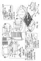
- FIG. 1Aillustrates a secure keypad device 100 constructed and operative in accordance with a preferred embodiment of the present invention.
- the secure keypad device 100includes a housing, preferably including a top housing element 102 and a bottom housing element 104 .
- Top housing element 102includes, on a top surface 106 thereof, a display window 108 , through which a display 109 may be viewed.
- An array 110 of keys 112is engageable on top surface 106 .
- An anti-tampering grid 122preferably formed of a multiplicity of anti-tampering electrical conductors 124 , is preferably provided to define a protective enclosure within the housing.
- a protective enclosuremay be defined within a secure integrated circuit 126 , which may be within or outside the protective enclosure defined by grid 122 .
- one or more conductor 130which interconnects a signal generator assembly 132 and a signal analysis assembly 134 , both of which are preferably located within the protective enclosure defined by grid 122 and may be located within a protective enclosure defined within secure integrated circuit 126 .
- a signal generator assembly 132 and a signal analysis assembly 134both of which are preferably located within the protective enclosure defined by grid 122 and may be located within a protective enclosure defined within secure integrated circuit 126 .
- a signal generator assembly 132 and a signal analysis assembly 134both of which are preferably located within the protective enclosure defined by grid 122 and may be located within a protective enclosure defined within secure integrated circuit 126 .
- FIGS. 1A-5For the sake of clarity and simplicity of explanation, signal diagrams are provided in FIGS. 1A-5 , all of which relate to an embodiment having a single conductor 130 .
- One or more conductor 130may form part of anti-tampering grid 122 as one or more of conductors 124 and alternatively may not. Alternatively, one or more of conductors 130 may be formed on a rigid or flexible printed circuit substrate or form part of an integrated circuit or hybrid circuit. Signal generator assembly 132 , one or more conductor 130 and signal analysis assembly 134 together provide tampering detection functionality, as will be described hereinbelow in greater detail.
- one or more conductor 130may be a part of a pair of conductors extending in parallel to each other, wherein one of the conductors of the pair of conductors is grounded. Alternatively, one or more conductor 130 may not form part of a pair of conductors running in parallel to each other. It is also appreciated that the one or more conductor 130 may be routed parallel to a ground plate. Alternatively, the one or more conductor 130 is not routed parallel to a ground plate.
- the tampering detection functionalitysenses signal variations which occur very quickly in response to tampering with one or more conductor 130 or its connection to either or both of assemblies 132 and 134 , typically within an elapsed time of approximately 100 ns and depending on the signal generator and comparator employed. These signal variations typically occur within an elapsed time which is less than 100 nanoseconds or even as short as 1 nanosecond.
- the elapsed time during which tampering responsive signal variations take placeis generally of the order of the time required for the signal to pass along the length of each conductor 130 or less.
- a preferred length of electrical conductor 130is about 75 in. for a signal having a rise/fall time of approximately 10 nanoseconds (ns).
- the signal analysis assembly 134preferably enables sensing tampering attempts in an electrical conductor 130 as short as 6 inches, wherein the signal has a rise/fall time of one nanosecond.
- the time required for an electrical signal to pass along a typical conductor 130 embodied in a conventional FR4 PCBis 140-180 picoseconds/inch (ps/in).
- signal generator assembly 132comprises a signal generator 150 , such as a Xilinx 7 Series FPGA, commercially available from Xilinx, Incorporated of San Jose, Calif., which outputs, via a Digital to Analog (D/A) converter 152 , such as a TI-DAC 5670, commercially available from Texas Instruments, operating at 2.4 Gigasamples/second, a signal typically having a rise time of the order of 10 ns and a duration of the order of 150 ns. This signal preferably is repeated every 1 ms. The time duration required for the signal to traverse a conductor 130 , here designated TD, is typically of the order of tens of nanoseconds.
- a simplified signal diagram illustrating the rise of the output of D/A converter 152appears at A. In this simplified example, the signal rises nearly instantaneously to a voltage V 1 , typically 3 volts.
- the signal output of D/A converter 152is applied to one or more conductor 130 via a resistor 154 and is supplied via the one or more conductor 130 to a junction C and thence to signal analysis assembly 134 , which also receives a signal timing input from signal generator assembly 132 .
- Signal analysis assembly 134may be embodied in a number of different ways, three examples of which are described hereinbelow and shown in FIG. 1A as Examples I, II and III.
- signal analysis assembly 134preferably comprises an Analog to Digital (A/D) converter 160 , such as an ADC12D18-x00, commercially available from National Semiconductor, which operates at 3.6 Giga samples per second, which receives a signal at junction C from one or more conductor 130 and supplies it to a signal comparator 162 , such as a NL27WZ86, commercially available from On-Semi, Phoenix Ariz., USA. Comparator 162 also receives a reference signal C from a reference signal memory 164 , which reference signal represents the signal at C in the absence of tampering. Should the signal received from one or more conductor 130 not match the reference signal in the signal reference memory 164 within predetermined tolerances, a tampering alarm indication is provided by the comparator 162 .
- A/DAnalog to Digital
- reference signal Cis identical to the input received by comparator 162 from A/D converter 160 and no alarm indication is provided.
- signal analysis assembly 134preferably comprises a microprocessor 170 , such as a TMS320C6X commercially available from Texas Instruments, which receives the signal at junction C via an A/D converter 172 .
- the input from A/D converter 172is supplied to Fast Fourier Transform (FFT) calculation functionality 174 of microprocessor 170 .
- FFT calculation functionality 174is supplied by FFT calculation functionality 174 to signal comparator functionality 176 of microprocessor 170 .
- Comparator functionality 176also receives a reference signal C from a FFT reference memory 178 , which FFT reference represents the signal at C in the absence of tampering. Should the FFT calculation result representing the signal received from one or more conductor 130 not match the FFT reference signal in the FFT reference memory 178 within predetermined tolerances, a tampering alarm indication is provided by the microprocessor 170 .
- the FFT reference stored in FFT reference memory 178is identical to the input received by comparator functionality 176 from FFT calculation functionality 174 and no alarm indication is provided.
- signal analysis assembly 134preferably comprises an analog comparator 180 , such as a ADA4960-1 differential amplifier, commercially available from Analog Devices, which receives an analog signal at junction C from one or more conductor 130 .
- Comparator 180also receives a reference signal C from a reference signal memory 182 via a D/A converter 184 , such as a TI-DAC 5670, commercially available from Texas Instruments, operating at 2.4 Gigasamples/second, which reference signal represents the signal at C in the absence of tampering. Should the signal received from one or more conductor 130 not match the reference signal in the signal reference memory 182 within predetermined tolerances, a tampering alarm indication is provided by the comparator 180 .
- an analog comparator 180such as a ADA4960-1 differential amplifier, commercially available from Analog Devices, which receives an analog signal at junction C from one or more conductor 130 .
- Comparator 180also receives a reference signal C from a reference signal memory 182 via a D/
- reference signal Cis identical to the input received by comparator 180 and no alarm indication is provided.
- signal generator assembly 132 and of signal analysis assembly 134preferably takes place continuously whether or not the secured keypad device is being used and whether or not it is in operation.
- any suitable signal having a fast rise or fallmay be employed. Although a square wave signal is illustrated, it is appreciated that the signal need not be a square wave. Different signal configurations may be employed at different times.
- FIG. 1Billustrates a secure keypad device 200 constructed and operative in accordance with another preferred embodiment of the present invention.
- the secure keypad device 200includes a housing, preferably including a top housing element 202 and a bottom housing element 204 .
- Top housing element 202includes, on a top surface 206 thereof, a display window 208 , through which a display 209 may be viewed.
- An array 210 of keys 212is engageable on top surface 206 .
- An anti-tampering grid 222preferably formed of a multiplicity of anti-tampering electrical conductors 224 , is preferably provided to define a protective enclosure within the housing.
- a protective enclosuremay be defined within a secure integrated circuit 226 , which may be within or outside the protective enclosure defined by grid 222 .
- one or more conductor 230which interconnects a signal generator assembly 232 and a signal analysis assembly 234 , both of which are preferably located within the protective enclosure defined by grid 222 and may be located within a protective enclosure defined within secure integrated circuit 226 .
- a signal generator assembly 232 and a signal analysis assembly 234are preferably located within the protective enclosure defined by grid 222 and may be located within a protective enclosure defined within secure integrated circuit 226 .
- One or more conductor 230may form part of anti-tampering grid 222 as one or more of conductors 224 and alternatively may not. Alternatively, one or more of conductors 230 may be formed on a rigid or flexible printed circuit substrate or form part of an integrated circuit or hybrid circuit. Signal generator assembly 232 , one or more conductor 230 and signal analysis assembly 234 together provide tampering detection functionality, as will be described hereinbelow in greater detail.
- one or more conductor 230may be a part of a pair of conductors extending in parallel to each other, wherein one of the conductors of the pair of conductors is grounded. Alternatively, one or more conductor 230 may not form part of a pair of conductors running in parallel to each other. It is also appreciated that the one or more conductor 230 may be routed parallel to a ground plate. Alternatively, the one or more conductor 230 is not routed parallel to a ground plate.
- the tampering detection functionalitysenses signal variations which occur very quickly in response to tampering with one or more conductor 230 or its connection to either or both of assemblies 232 and 234 , typically within an elapsed time of approximately 100 ns and depending on the signal generator and comparator employed. These signal variations typically occur within an elapsed time which is less than 100 nanoseconds or even as short as 1 nanosecond.
- the elapsed time during which tampering responsive signal variations take placeis generally of the order of the time required for the signal to pass along the length of each conductor 230 or less.
- a preferred length of electrical conductor 230is about 75 in. for a signal having a rise/fall time of approximately 10 ns.
- the signal analysis assembly 234preferably enables sensing tampering attempts in an electrical conductor 230 as short as 6 inches, wherein the signal has a rise/fall time of a few nanoseconds.
- the time required for an electrical signal to pass along a typical conductor 230 embodied in a conventional FR4 PCBis 140-180 ps/in.
- signal generator assembly 232comprises a signal generator 250 , such as a Xilinx 7 Series FPGA, commercially available from Xilinx, Incorporated of San Jose, Calif., which outputs, via a D/A converter 252 , such as a TI-DAC 5670, commercially available from Texas Instruments, operating at 2.4 Gigasamples/second, a signal typically having a rise time of the order of 10 ns and a duration of the order of 150 ns. This signal preferably is repeated every 1 ms. The time duration required for the signal to traverse a conductor 230 , here designated TD, is typically of the order of tens of nanoseconds.
- a simplified signal diagram illustrating the rise of the output of D/A converter 252appears at A. In this simplified example, the signal rises nearly instantaneously to a voltage V 1 , typically 3 volts.
- the signal output of D/A converter 252is applied to one or more conductor 230 via a resistor 254 .
- the signalpasses along one or more conductor 230 and is reflected back along one or more conductor 230 to a junction between the one or more conductor 230 and resistor 254 , designated B.
- This signalis supplied to signal analysis assembly 234 , which also receives a signal timing input from signal generator assembly 232 .
- a simplified signal diagram illustrating the rise of the signal supplied from junction B to signal analysis assembly 234appears as signal diagram B. It is seen that the signal at B rises generally instantaneously to a voltage of approximately 0.5V 1 and includes harmonics about voltage 0.5V 1 . Following a time duration 2 TD, which corresponds to two traversals of one or more conductor 230 , the signal rises generally instantaneously to voltage V 1 and includes harmonics about voltage V 1 .
- Signal analysis assembly 234may be embodied in a number of different ways, three examples of which are described hereinbelow and shown in FIG. 1B as Examples I, II and III.
- signal analysis assembly 234preferably comprises an A/D converter 260 , such as an ADC12D1800, commercially available from National Semiconductor, which operates at 3.6 Giga samples per second, which receives a signal at junction B from one or more conductor 230 and supplies it to a signal comparator 262 , such as a NL27WZ86, commercially available from On-Semi, Phoenix Ariz., USA.
- Comparator 262also receives a reference signal B from a reference signal memory 264 , which reference signal represents the signal at B in the absence of tampering. Should the signal received from one or more conductor 230 not match the reference signal in the signal reference memory 264 within predetermined tolerances, a tampering alarm indication is provided by the comparator 262 .
- reference signal Bis identical to the input received by comparator 262 from A/D converter 260 and no alarm indication is provided.
- signal analysis assembly 234preferably comprises a microprocessor 270 , such as a TMS320C6X commercially available from Texas Instruments, which receives the signal at junction B via an A/D converter 272 .
- the input from A/D converter 272is supplied to Fast Fourier Transform (FFT) calculation functionality 274 of microprocessor 270 .
- FFT calculation functionality 274is supplied by FFT calculation functionality 274 to signal comparator functionality 276 of microprocessor 270 .
- Comparator functionality 276also receives a reference signal B from a FFT reference memory 278 , which FFT reference represents the signal at B in the absence of tampering. Should the FFT calculation result representing the signal received from one or more conductor 230 not match the FFT reference signal in the FFT reference memory 278 within predetermined tolerances, a tampering alarm indication is provided by the microprocessor 270 .
- the FFT referenceis identical to the input received by comparator functionality 276 from FFT calculation functionality 274 and no alarm indication is provided.
- signal analysis assembly 234preferably comprises an analog comparator 280 , such as an ADA4960-1 differential amplifier, commercially available from Analog Devices, which receives an analog signal at junction B from one or more conductor 230 .
- Comparator 280also receives a reference signal B from a reference signal memory 282 via a D/A converter 284 , such as a TI-DAC 5670, commercially available from Texas Instruments, operating at 2.4 Gigasamples/second, which reference signal represents the signal at B in the absence of tampering. Should the signal received from one or more conductor 230 not match the reference signal in the signal reference memory 282 within predetermined tolerances, a tampering alarm indication is provided by the comparator 280 .
- an analog comparator 280such as an ADA4960-1 differential amplifier, commercially available from Analog Devices, which receives an analog signal at junction B from one or more conductor 230 .
- Comparator 280also receives a reference signal B from a reference signal memory 28
- reference signal Bis identical to the input received by comparator 280 and no alarm indication is provided.
- signal generator assembly 232 and of signal analysis assembly 234preferably takes place continuously whether or not the secured keypad device is being used and whether or not it is in operation.
- any suitable signal having a fast rise or fallmay be employed. Although a square wave signal is illustrated, it is appreciated that the signal need not be a square wave. Different signal configurations may be employed at different times.
- FIG. 1Cillustrates a secure keypad device 300 constructed and operative in accordance with yet another preferred embodiment of the present invention.
- the secure keypad device 300includes a housing, preferably including a top housing element 302 and a bottom housing element 304 .
- Top housing element 302includes, on a top surface 306 thereof, a display window 308 , through which a display 309 may be viewed.
- An array 310 of keys 312is engageable on top surface 306 .
- An anti-tampering grid 322preferably formed of a multiplicity of anti-tampering electrical conductors 324 , is preferably provided to define a protective enclosure within the housing.
- a protective enclosuremay be defined within a secure integrated circuit 326 , which may be within or outside the protective enclosure defined by grid 322 .
- one or more conductor 330which interconnects a signal generator assembly 332 and a signal analysis assembly 334 , both of which are preferably located within the protective enclosure defined by grid 322 and may be located within a protective enclosure defined within secure integrated circuit 326 .
- a signal generator assembly 332 and a signal analysis assembly 334are preferably located within the protective enclosure defined by grid 322 and may be located within a protective enclosure defined within secure integrated circuit 326 .
- One or more conductor 330may form part of anti-tampering grid 322 as one or more of conductors 324 and alternatively may not. Alternatively, one or more of conductors 330 may be formed on a rigid or flexible printed circuit substrate or form part of an integrated circuit or hybrid circuit. Signal generator assembly 332 , one or more conductor 330 and signal analysis assembly 334 together provide tampering detection functionality, as will be described hereinbelow in greater detail.
- one or more conductor 330may be a part of a pair of conductors extending in parallel to each other, wherein one of the conductors of the pair of conductors is grounded. Alternatively, one or more conductor 330 may not form part of a pair of conductors running in parallel to each other. It is also appreciated that the one or more conductor 330 may be routed parallel to a ground plate. Alternatively, the one or more conductor 330 is not routed parallel to a ground plate.
- the tampering detection functionalitysenses signal variations which occur very quickly in response to tampering with one or more conductor 330 or its connection to either or both of assemblies 332 and 334 , typically within an elapsed time of approximately 100 ns and depending on the signal generator and comparator employed. These signal variations typically occur within an elapsed time which is less than 100 nanoseconds or even as short as 1 nanosecond.
- the elapsed time during which tampering responsive signal variations take placeis generally of the order of the time required for the signal to pass along the length of each conductor 330 or less.
- a preferred length of electrical conductor 330is about 75 in. for a signal having a rise/fall time of approximately 10 ns.
- the signal analysis assembly 334preferably enables sensing tampering attempts in an electrical conductor 330 as short as 6 inches, wherein the signal has a rise/fall time of a few nanoseconds.
- the time required for an electrical signal to pass along a typical conductor 330 embodied in a conventional FR4 PCBis 140-180 ps/in.
- signal generator assembly 332comprises a signal generator 350 , such as a Xilinx 7 Series FPGA, commercially available from Xilinx, Incorporated of San Jose, Calif., which outputs, via a D/A converter 352 , such as a TI-DAC 5670, commercially available from Texas Instruments, operating at 2.4 Gigasamples/second, a signal typically having a rise time of the order of 10 ns and a duration of the order of 150 ns. This signal preferably is repeated every 1 ms. The time duration required for the signal to traverse a conductor 330 , here designated TD, is typically of the order of tens of nanoseconds.
- a simplified signal diagram illustrating the rise of the output of D/A converter 352appears at A. In this simplified example, the signal rises nearly instantaneously to a voltage V 1 , typically 3 volts.
- the signal output of D/A converter 352is applied to one or more conductor 330 via a resistor 354 and is supplied via the one or more conductor 330 to a junction C and thence to a signal analysis subassembly 355 of signal analysis assembly 334 , which also receives a signal timing input from signal generator assembly 332 .
- a simplified signal diagram illustrating the rise of a signal supplied from one conductor 330 to signal analysis assembly 334appears as signal diagram C. It is seen that the rise of the signal at C is delayed from time 0 by time duration TD and, where the resistance of conductor 330 is generally equal to the resistance of resistor 354 , the resulting signal rises nearly instantaneously after delay TD to V 1 and includes harmonics about voltage V 1 .
- the signalpasses along conductor 330 and a portion thereof is reflected back along conductor 330 to a junction between the conductor 330 and resistor 354 , designated B.
- a signal from junction Bis supplied to a signal analysis subassembly 356 of signal analysis assembly 334 , which also receives a signal timing input from signal generator assembly 332 .
- a simplified signal diagram illustrating the rise of the signal supplied from junction B to signal analysis subassembly 356appears as signal diagram B. It is seen that the signal at B rises generally instantaneously to a voltage of approximately 0.5V 1 and includes harmonics about voltage 0.5V 1 . Following a time duration 2 TD, which corresponds to two traversals of conductor 330 , the signal rises generally instantaneously to voltage V 1 and includes harmonics about voltage V 1 .
- Each of subassemblies 355 and 356 of signal analysis assembly 334may be embodied in a number of different ways, three examples of which are described hereinbelow and shown in FIG. 1C as Examples I, II and III.
- one or both of subassemblies 355 and 356 of signal analysis assembly 334preferably comprises an A/D converter 360 , such as an ADC112D1800, commercially available from National Semiconductor, which operates at 3.6 Giga samples per second, which receives a signal at junction C or junction B, respectively, from one or more conductor 330 and supplies it to a signal comparator 362 , such as a NL27WZ86, commercially available from On-Semi, Phoenix Ariz., USA.
- Comparator 362also receives a reference signal C or a reference signal B from a reference signal memory 364 , which reference signal represents the signal at C or B, respectively, in the absence of tampering. Should the signal received from one or more conductor 330 not match the reference signal in the signal reference memory 364 within predetermined tolerances, a tampering alarm indication is provided by the comparator 362 .
- reference signal C or reference signal Bis identical to the input received by comparator 362 from A/D converter 360 and no alarm indication is provided.
- one or both of subassemblies 355 and 356 of signal analysis assembly 334preferably comprises a microprocessor 370 , such as a TMS320C6X commercially available from Texas Instruments, which receives the signal at junction C or junction B via an A/D converter 372 .
- the input from A/D converter 372is supplied to Fast Fourier Transform (FFT) calculation functionality 374 of microprocessor 370 .
- FFT calculation functionality 374is supplied by FFT calculation functionality 374 to signal comparator functionality 376 of microprocessor 370 .
- Comparator functionality 376also receives a reference signal C or a reference signal B from a FFT reference memory 378 , which FFT reference represents the signal at C or B, respectively, in the absence of tampering. Should the FFT calculation result representing the signal received from one or more conductor 330 not match the FFT reference signal in the FFT reference memory 378 within predetermined tolerances, a tampering alarm indication is provided by the microprocessor 370 .
- the FFT referenceis identical to the input received by comparator functionality 376 from FFT calculation functionality 374 and no alarm indication is provided.
- one or both of subassemblies 355 and 356 of signal analysis assembly 334preferably comprises an analog comparator 380 , such as an ADA4960-1 differential amplifier, commercially available from Analog Devices, which receives an analog signal at junction C or junction B, respectively, from one or more conductor 330 .
- Comparator 380also receives a reference signal C or a reference signal B from a reference signal memory 382 via a D/A converter 384 , such as a TI-DAC 5670, commercially available from Texas Instruments, operating at 2.4 Gigasamples/second, which reference signal represents the signal at C or B, respectively, in the absence of tampering. Should the signal received from one or more conductor 330 not match the reference signal in the signal reference memory 382 within predetermined tolerances, a tampering alarm indication is provided by the comparator 380 .
- reference signal C or reference Bis identical to the input received by comparator 380 and no alarm indication is provided.
- the alarm indications from respective signal analysis subassemblies 355 and 356are preferably supplied to alarm logic 390 , which may provide an alarm output in response to any suitable combination of alarm indications.
- signal generator assembly 332 and of signal analysis assembly 334preferably takes place continuously whether or not the secured keypad device is being used and whether or not it is in operation.
- any suitable signal having a fast rise or fallmay be employed. Although a square wave signal is illustrated, it is appreciated that the signal need not be a square wave. Different signal configurations may be employed at different times.
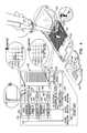
- FIG. 1Dillustrates a secure keypad device 400 constructed and operative in accordance with still another preferred embodiment of the present invention.
- the secure keypad device 400includes a housing, preferably including a top housing element 402 and a bottom housing element 404 .
- Top housing element 402includes, on a top surface 406 thereof, a display window 408 , through which a display 409 may be viewed.
- An array 410 of keys 412is engageable on top surface 406 .
- An anti-tampering grid 422preferably formed of a multiplicity of anti-tampering electrical conductors 424 , is preferably provided to define a protective enclosure within the housing.
- a protective enclosuremay be defined within a secure integrated circuit 426 , which may be within or outside the protective enclosure defined by grid 422 .
- one or more conductor 430which interconnects a signal generator assembly 432 and a signal analysis assembly 434 , both of which are preferably located within the protective enclosure defined by grid 422 and may be located within a protective enclosure defined within secure integrated circuit 426 .
- a signal generator assembly 432 and a signal analysis assembly 434are preferably located within the protective enclosure defined by grid 422 and may be located within a protective enclosure defined within secure integrated circuit 426 .
- One or more conductor 430may form part of anti-tampering grid 422 as one or more of conductors 424 and alternatively may not. Alternatively, one or more of conductors 430 may be formed on a rigid or flexible printed circuit substrate or form part of an integrated circuit or hybrid circuit. Signal generator assembly 432 , one or more conductor 430 and signal analysis assembly 434 together provide tampering detection functionality, as will be described hereinbelow in greater detail.
- one or more conductor 430may be a part of a pair of conductors extending in parallel to each other, wherein one of the conductors of the pair of conductors is grounded. Alternatively, one or more conductor 430 may not form part of a pair of conductors running in parallel to each other. It is also appreciated that the one or more conductor 430 may be routed parallel to a ground plate. Alternatively, the one or more conductor 430 is not routed parallel to a ground plate.
- the tampering detection functionalitysenses signal variations which occur very quickly in response to tampering with one or more conductor 430 or its connection to either or both of assemblies 432 and 434 , typically within an elapsed time of approximately 100 ns and depending on the signal generator and comparator employed. These signal variations typically occur within an elapsed time which is less than 100 nanoseconds or even as short as 1 nanosecond.
- the elapsed time during which tampering responsive signal variations take placeis generally of the order of the time required for the signal to pass along the length of each conductor 430 or less.
- a preferred length of electrical conductor 430is about 75 in. for a signal having a rise/fall time of approximately 10 ns.
- the signal analysis assembly 434preferably enables sensing tampering attempts in an electrical conductor 430 as short as 6 inches, wherein the signal has a rise/fall time of a few nanoseconds.
- the time required for an electrical signal to pass along a typical conductor 430 embodied in a conventional FR4 PCBis 140-180 ps/in.
- signal generator assembly 432comprises a signal generator 450 , such as a Xilinx 7 Series FPGA, commercially available from Xilinx, Incorporated of San Jose, Calif., which outputs, via a D/A converter 452 , such as a TI-DAC 5670, commercially available from Texas Instruments, operating at 2.4 Gigasamples/second, a signal typically having a rise time of the order of 10 ns and a duration of the order of 150 ns. This signal preferably is repeated every 1 ms. The time duration required for the signal to traverse a conductor 430 , here designated TD, is typically of the order of tens of nanoseconds.
- a simplified signal diagram illustrating the rise of the output of D/A converter 452appears at A. In this simplified example, the signal rises nearly instantaneously to a voltage V 1 , typically 3 volts.
- the signal output of D/A converter 452is applied to one or more conductor 430 via a resistor 454 and is supplied via the one or more conductor 430 to a junction C and thence to a signal analysis subassembly 455 of signal analysis assembly 434 , which also receives a signal timing input from signal generator assembly 432 .
- a simplified signal diagram illustrating the rise of a signal supplied from one conductor 430 to signal analysis assembly 434appears as signal diagram C. It is seen that the rise of the signal at C is delayed from time 0 by time duration TD and, where the resistance of conductor 430 is generally equal to the resistance of resistor 454 , the resulting signal rises nearly instantaneously after delay TD to V 1 and includes harmonics about voltage V 1 .
- the signalpasses along conductor 430 and a portion thereof is reflected back along conductor 430 to a junction between the conductor 430 and resistor 454 , designated B.
- This signalis supplied to a signal analysis subassembly 456 of signal analysis assembly 434 , which also receives a signal timing input from signal generator assembly 432 .
- a simplified signal diagram illustrating the rise of the signal supplied from junction B to signal analysis subassembly 456appears as signal diagram B. It is seen that the signal at B rises generally instantaneously to a voltage of approximately 0.5V 1 and includes harmonics about voltage 0.5V 1 . Following a time duration 2 TD, which corresponds to two traversals of conductor 430 , the signal rises generally instantaneously to voltage V 1 and includes harmonics about voltage V 1 .
- signals from junctions B and Care also supplied to a signal analysis subassembly 457 , which forms part of signal analysis assembly 434 .
- Signal analysis subassembly 457also receives a signal timing input from signal generator assembly 432 .
- Signal analysis subassembly 457preferably includes a difference circuit 458 which provides a signal representing the difference between signals B and C.
- the output of the difference circuit 458is preferably supplied via an A/D converter 459 to a comparator 460 which also receives a reference signal
- is identical to the input received by comparator 460 from A/D converter 459 and no alarm indication is provided. It is appreciated that in a further alternative embodiment either or both of signal analysis subassemblies 455 and 456 may be obviated.
- Each of subassemblies 455 and 456 of signal analysis assembly 434may be embodied in a number of different ways, three examples of which are described hereinbelow and shown in FIG. 1D as Examples I, II and III.
- one or both of subassemblies 455 and 456 of signal analysis assembly 434preferably comprises an A/D converter 462 , such as an ADC12D1800, commercially available from National Semiconductor, which operates at 3.6 Giga samples per second, which receives a signal at junction C or junction B, respectively, from one or more conductor 430 and supplies it to a signal comparator 463 , such as a NL27WZ86, commercially available from On-Semi, Phoenix Ariz., USA. Comparator 463 also receives a reference signal C or a reference signal B from a reference signal memory 464 , which reference signal represents the signal at C or B, respectively, in the absence of tampering. Should the signal received from one or more conductor 430 not match the reference signal in the signal reference memory 464 within predetermined tolerances, a tampering alarm indication is provided by the comparator 463 .
- A/D converter 462such as an ADC12D1800, commercially available from National Semi
- reference signal C or reference signal Bis identical to the input received by comparator 463 from A/D converter 462 and no alarm indication is provided.
- one or both of subassemblies 455 and 456 of signal analysis assembly 434preferably comprises a microprocessor 470 , such as a TMS320C6X commercially available from Texas Instruments, which receives the signal at junction C or junction B via an A/D converter 472 .
- the input from A/D converter 472is supplied to Fast Fourier Transform (FFT) calculation functionality 474 of microprocessor 470 .
- FFT calculation functionality 474is supplied by FFT calculation functionality 474 to signal comparator functionality 476 of microprocessor 470 .
- Comparator functionality 476also receives a reference signal C or a reference signal B from a FFT reference memory 478 , which FFT reference represents the signal at C or B, respectively, in the absence of tampering. Should the FFT calculation result representing the signal received from one or more conductor 430 not match the FFT reference signal in the FFT reference memory 478 within predetermined tolerances, a tampering alarm indication is provided by the microprocessor 470 .
- the FFT referenceis identical to the input received by comparator functionality 476 from FFT calculation functionality 474 and no alarm indication is provided.
- one or both of subassemblies 455 and 456 of signal analysis assembly 434preferably comprises an analog comparator 480 , such as an ADA4960-1 differential amplifier, commercially available from Analog Devices, which receives an analog signal at junction C or junction B, respectively, from one or more conductor 430 .
- Comparator 480also receives a reference signal C or a reference signal B from a reference signal memory 482 via a D/A converter 484 , such as a TI-DAC 5670, commercially available from Texas Instruments, operating at 2.4 Gigasamples/second, which reference signal represents the signal at C or B, respectively, in the absence of tampering. Should the signal received from one or more conductor 430 not match the reference signal in the signal reference memory 482 within predetermined tolerances, a tampering alarm indication is provided by the comparator 480 .
- reference signal C or reference Bis identical to the input received by comparator 480 and no alarm indication is provided.
- signal analysis subassembly 457 downstream of difference circuit 458may alternatively be constructed and operative in accordance with any of Examples I, II and III described hereinabove.
- the alarm indications from respective signal analysis subassemblies 455 , 456 and 457are preferably supplied to alarm logic 490 , which may provide an alarm output in response to any suitable combination of alarm indications.
- signal generator assembly 432 and of signal analysis assembly 434preferably takes place continuously whether or not the secured keypad device is being used and whether or not it is in operation.
- any suitable signal having a fast rise or fallmay be employed. Although a square wave signal is illustrated, it is appreciated that the signal need not be a square wave. Different signal configurations may be employed at different times.
- FIGS. 2 , 3 , 4 and 5are simplified schematic illustrations of the operation of the secure keypad device of FIG. 1D responsive to four different types of tampering.
- FIGS. 2-5relate to an embodiment of FIG. 1D having a single conductor 430 and wherein the signal analysis assembly 434 is constructed and operative in accordance with Example I, as described hereinabove. It is appreciated that the explanations below which relate to FIGS. 2 , 3 , 4 and 5 are also applicable with appropriate modifications to the embodiments of any of FIGS. 1A-1C and to any of Examples I, II and III and to any suitable number of conductors 130 , 230 , 330 and 430 .
- FIG. 2is a simplified schematic illustration of the operation of the secure keypad device of FIG. 1D responsive to a first type of tampering.
- the conductor 430is tampered with by contact therewith as by a metal object and/or an object having inductance or capacitance, as symbolically shown at II.
- This tamperingcauses a change in the signals at junctions B and C, typically as shown, respectively, in signal diagrams B—Tampered and C—Tampered. Normally the difference
- Comparators 463 , of signal analysis subassemblies 455 and 456 , and 460 , of signal analysis subassembly 457which receive respective reference inputs C, B and
- Alarm logic 490provides a suitable alarm indication in accordance with its logic function.
- FIG. 3is a simplified schematic illustration of the operation of the secure keypad device of FIG. 1D responsive to a second type of tampering.
- the conductor 430is cut, as symbolically shown at III.
- This tamperingcauses disappearance of the signal at C and typically produces a change in the signal at B, as shown, respectively, in signal diagrams C—Tampered and B—Tampered.
- also changes.
- Comparators 463 , of signal analysis subassemblies 455 and 456 , and 460 , of signal analysis subassembly 457which receive respective reference inputs C, B and
- Alarm logic 490provides a suitable alarm indication in accordance with its logic function.
- FIG. 4is a simplified schematic illustration of the operation of the secure keypad device of FIG. 1D responsive to a third type of tampering.
- the conductor 430is shorted to ground at junction C, as symbolically shown at IV.
- This tamperingcauses disappearance of the signal at C and typically produces a change in the signal at B, as shown, respectively, in signal diagrams C—Tampered and B—Tampered.
- also changes.
- Comparators 463 , of signal analysis subassemblies 455 and 456 , and 460 of signal analysis subassembly 457which receive respective reference inputs C, B and
- Alarm logic 490provides a suitable alarm indication in accordance with its logic function.
- FIG. 5is a simplified schematic illustration of the operation of the secure keypad device of FIG. 1D responsive to a fourth type of tampering.
- the junctions B and Care shorted together, as symbolically shown at V.
- This tamperingcauses change in the signals at B and C, as shown, respectively, in signal diagrams B—Tampered and C—Tampered.
- also typically changes
- Comparators 463 , of signal analysis subassemblies 455 and 456 , and 460 , of signal analysis subassembly 457which receive respective reference inputs C, B and
- Alarm logic 490provides a suitable alarm indication in accordance with its logic function. This logic function may be any suitable logic function which provides an alarm output in response to a combination of alarm indications which is indicative of tampering with an acceptably high rate of accuracy and an acceptably low rate of false alarms.
Landscapes
- Physics & Mathematics (AREA)
- General Physics & Mathematics (AREA)
- Engineering & Computer Science (AREA)
- Computer Hardware Design (AREA)
- General Engineering & Computer Science (AREA)
- Burglar Alarm Systems (AREA)
Abstract
Description
Claims (15)
Priority Applications (2)
| Application Number | Priority Date | Filing Date | Title |
|---|---|---|---|
| US12/848,471US8405506B2 (en) | 2010-08-02 | 2010-08-02 | Secure data entry device |
| US13/782,095US8710987B2 (en) | 2010-08-02 | 2013-03-01 | Secure data entry device |
Applications Claiming Priority (1)
| Application Number | Priority Date | Filing Date | Title |
|---|---|---|---|
| US12/848,471US8405506B2 (en) | 2010-08-02 | 2010-08-02 | Secure data entry device |
Related Child Applications (1)
| Application Number | Title | Priority Date | Filing Date |
|---|---|---|---|
| US13/782,095ContinuationUS8710987B2 (en) | 2010-08-02 | 2013-03-01 | Secure data entry device |
Publications (2)
| Publication Number | Publication Date |
|---|---|
| US20120025983A1 US20120025983A1 (en) | 2012-02-02 |
| US8405506B2true US8405506B2 (en) | 2013-03-26 |
Family
ID=45526161
Family Applications (2)
| Application Number | Title | Priority Date | Filing Date |
|---|---|---|---|
| US12/848,471Active2031-06-09US8405506B2 (en) | 2010-08-02 | 2010-08-02 | Secure data entry device |
| US13/782,095ActiveUS8710987B2 (en) | 2010-08-02 | 2013-03-01 | Secure data entry device |
Family Applications After (1)
| Application Number | Title | Priority Date | Filing Date |
|---|---|---|---|
| US13/782,095ActiveUS8710987B2 (en) | 2010-08-02 | 2013-03-01 | Secure data entry device |
Country Status (1)
| Country | Link |
|---|---|
| US (2) | US8405506B2 (en) |
Families Citing this family (9)
| Publication number | Priority date | Publication date | Assignee | Title |
|---|---|---|---|---|
| US9013336B2 (en) | 2008-01-22 | 2015-04-21 | Verifone, Inc. | Secured keypad devices |
| US8595514B2 (en) | 2008-01-22 | 2013-11-26 | Verifone, Inc. | Secure point of sale terminal |
| US8432300B2 (en)* | 2009-03-26 | 2013-04-30 | Hypercom Corporation | Keypad membrane security |
| US8358218B2 (en)* | 2010-03-02 | 2013-01-22 | Verifone, Inc. | Point of sale terminal having enhanced security |
| US8330606B2 (en) | 2010-04-12 | 2012-12-11 | Verifone, Inc. | Secure data entry device |
| CN101944244B (en)* | 2010-08-27 | 2013-11-06 | 广州广电运通金融电子股份有限公司 | Encryption keyboard capable of preventing illegal disassembly |
| US9213869B2 (en) | 2013-10-04 | 2015-12-15 | Verifone, Inc. | Magnetic stripe reading device |
| US9595174B2 (en) | 2015-04-21 | 2017-03-14 | Verifone, Inc. | Point of sale terminal having enhanced security |
| DE102017211690B4 (en) | 2017-07-07 | 2020-07-16 | Bayerische Motoren Werke Aktiengesellschaft | System for reducing load peaks in an electrical system |
Citations (82)
| Publication number | Priority date | Publication date | Assignee | Title |
|---|---|---|---|---|
| GB892198A (en) | 1960-06-07 | 1962-03-21 | American District Telegraph Co | Electrical protection system |
| US3466643A (en) | 1966-03-18 | 1969-09-09 | Carlton Swain Moorefield | Transmission line tampering alarm system |
| DE2241738A1 (en) | 1971-09-22 | 1973-03-29 | Securiton Ag | SHOULDER DISTRIBUTORS FOR ALARM SYSTEMS |
| US3735353A (en) | 1971-10-28 | 1973-05-22 | Johnson Service Co | Alarm transmission line security system utilizing pseudo random encoding |
| US3818330A (en) | 1972-08-17 | 1974-06-18 | Hitachi Ltd | Device having a bridge circuit for detecting faults in an electric network |
| US4486637A (en) | 1982-06-28 | 1984-12-04 | Northern Telecom Limited | Pushbutton switch assembly |
| US4527030A (en) | 1980-11-06 | 1985-07-02 | Preh Elektrofeinmechanische Werke, Jakob Preh Nachf., Gmbh & Co. | Keyboard |
| US4593384A (en) | 1984-12-21 | 1986-06-03 | Ncr Corporation | Security device for the secure storage of sensitive data |
| US4749368A (en) | 1986-04-03 | 1988-06-07 | E. I. Du Pont De Nemours And Company | Contact strip terminal |
| US4807284A (en) | 1986-09-24 | 1989-02-21 | Ncr Corporation | Security device for sensitive data |
| US4847595A (en) | 1986-12-08 | 1989-07-11 | Atsumi Denki Kabushiki Kaisha | Alarm system |
| EP0325768A2 (en) | 1988-01-11 | 1989-08-02 | American Cyanamid Company | Non-reverting rna viruses |
| EP0375545A1 (en) | 1988-12-20 | 1990-06-27 | Bull S.A. | Device to protect an electronic card and its use to protect a reading terminal of a magnetic and/or microprocessor card |
| US5086292A (en) | 1989-10-31 | 1992-02-04 | Iris Systems Inc. | Tamper detection device for utility meter |
| US5117222A (en)* | 1990-12-27 | 1992-05-26 | Guardian Technologies, Inc. | Tamper indicating transmitter |
| US5237307A (en) | 1991-11-27 | 1993-08-17 | The United States Of America As Represented By The United States Department Of Energy | Non-contact tamper sensing by electronic means |
| US5239664A (en) | 1988-12-20 | 1993-08-24 | Bull S.A. | Arrangement for protecting an electronic card and its use for protecting a terminal for reading magnetic and/or microprocessor cards |
| US5353350A (en) | 1989-10-03 | 1994-10-04 | University Of Technology | Electro-active cradle circuits for the detection of access or penetration |
| US5506566A (en)* | 1993-05-06 | 1996-04-09 | Northern Telecom Limited | Tamper detectable electronic security package |
| US5559311A (en) | 1994-12-27 | 1996-09-24 | General Motors Corporation | Dual detent dome switch assembly |
| US5586042A (en) | 1993-03-15 | 1996-12-17 | Hughey-Pisau, Ltd. | Apparatus and methods for measuring and detecting variations in the value of a capacitor |
| US5627520A (en) | 1995-07-10 | 1997-05-06 | Protell Systems International, Inc. | Tamper detect monitoring device |
| US5675319A (en) | 1996-04-26 | 1997-10-07 | David Sarnoff Research Center, Inc. | Tamper detection device |
| US5861662A (en) | 1997-02-24 | 1999-01-19 | General Instrument Corporation | Anti-tamper bond wire shield for an integrated circuit |
| US5877547A (en) | 1994-11-17 | 1999-03-02 | Schlumberger Industries | Active security device including an electronic memory |
| US5998858A (en) | 1995-07-20 | 1999-12-07 | Dallas Semiconductor Corporation | Microcircuit with memory that is protected by both hardware and software |
| WO2001063994A2 (en) | 2000-02-23 | 2001-08-30 | Iridian Technologies, Inc. | Tamper proof case for electronic devices having memories with sensitive information |
| US6288640B1 (en) | 1995-12-15 | 2001-09-11 | GAGNON ANDRé | Open transmission line intrusion detection system using frequency spectrum analysis |
| US6359338B1 (en) | 1999-07-09 | 2002-03-19 | Oki Electric Industry Co., Ltd. | Semiconductor apparatus with self-security function |
| JP2002108711A (en) | 2000-09-29 | 2002-04-12 | Tamura Electric Works Ltd | Data processor and data processing method |
| US6396400B1 (en) | 1999-07-26 | 2002-05-28 | Epstein, Iii Edwin A. | Security system and enclosure to protect data contained therein |
| US6414884B1 (en) | 2000-02-04 | 2002-07-02 | Lucent Technologies Inc. | Method and apparatus for securing electronic circuits |
| GB2372363A (en) | 2000-12-01 | 2002-08-21 | Peter Gwynne | Security device having a capacitive sensor |
| US6438825B1 (en) | 1995-03-28 | 2002-08-27 | Intel Corporation | Method to prevent intrusions into electronic circuitry |
| US6463263B1 (en) | 1999-02-01 | 2002-10-08 | Telefonaktiebolaget Lm Ericsson (Publ) | Communication station |
| US6466118B1 (en) | 2002-04-17 | 2002-10-15 | Duraswitch Industries, Inc. | Overlay electrical conductor for a magnetically coupled pushbutton switch |
| JP2003100169A (en) | 2001-09-21 | 2003-04-04 | Fuji Denshi Kogyo Kk | Dome contact sheet and switch with click action |
| US6563488B1 (en) | 1997-09-29 | 2003-05-13 | Varatouch Technology Incorporated | Pointing device with integrated switch |
| US6646565B1 (en) | 2000-06-01 | 2003-11-11 | Hewlett-Packard Development Company, L.P. | Point of sale (POS) terminal security system |
| US6669100B1 (en) | 2002-06-28 | 2003-12-30 | Ncr Corporation | Serviceable tamper resistant PIN entry apparatus |
| US20040031673A1 (en) | 2002-05-23 | 2004-02-19 | Levy David H. | Keypads and key switches |
| EP1421549A1 (en) | 2001-08-31 | 2004-05-26 | Trintech Limited | A pin pad |
| EP1432031A1 (en) | 2002-12-20 | 2004-06-23 | Lipman Electronic Engineering Ltd. | Anti-tampering enclosure for electronic circuitry |
| US20040118670A1 (en) | 2002-12-03 | 2004-06-24 | Sung-Sun Park | Rotation key device for a portable terminal |
| DE60101096T2 (en) | 2000-03-17 | 2004-07-01 | Thales E-Transactions S.A. | ELASTOMER MEMBRANE AGAINST PENETRATION FOR SECURED ELECTRONIC HOUSINGS |
| US6830182B2 (en) | 2002-04-11 | 2004-12-14 | Cis Eletronica Industria E Comercio Ltda. | Magnetic card reader |
| US6874092B1 (en) | 1998-10-06 | 2005-03-29 | Ricoh Corporation | Method and apparatus for erasing data after tampering |
| US20050081049A1 (en) | 2003-10-09 | 2005-04-14 | Takeshi Nakayama | Mobile terminal, circuit board, circuit board design aiding apparatus and method, design aiding program, and storage medium having stored therein design aiding program |
| US6912280B2 (en) | 2002-07-22 | 2005-06-28 | Sony Ericsson Mobile Communications Ab | Keypad device |
| US20050184870A1 (en) | 2004-02-25 | 2005-08-25 | Dmatek, Ltd. | Method and apparatus for portable transmitting devices |
| US6936777B1 (en) | 2004-03-12 | 2005-08-30 | Fuji Electronics Industries Co., Ltd. | Two-step switch |
| GB2411756A (en) | 2004-03-04 | 2005-09-07 | Dione Plc | Secure card reader |
| WO2005086546A2 (en) | 2004-03-04 | 2005-09-15 | Lipman Electronics Engineering Limited | Secure card reader |
| US6995353B2 (en)* | 2004-01-09 | 2006-02-07 | Beinhocker Gilbert D | Tamper-proof container |
| US20060049256A1 (en) | 2004-09-07 | 2006-03-09 | Clay Von Mueller | Transparently securing data for transmission on financial networks |
| US20060049255A1 (en) | 2004-09-07 | 2006-03-09 | Clay Von Mueller | Secure magnetic stripe reader for handheld computing and method of using same |
| US20060066456A1 (en)* | 1999-08-09 | 2006-03-30 | Jonker Rene T | Revenue meter with power quality features |
| EP1676182A1 (en) | 2003-10-24 | 2006-07-05 | Trintech Limited | Circuit security |
| US20060192653A1 (en) | 2005-02-18 | 2006-08-31 | Paul Atkinson | Device and method for selectively controlling the utility of an integrated circuit device |
| US7170409B2 (en) | 2003-03-06 | 2007-01-30 | Cypak Ab | Tamper evident packaging |
| US20070040674A1 (en) | 2005-08-16 | 2007-02-22 | Honeywell International, Inc. | Conductive tamper switch for security devices |
| US20070102272A1 (en) | 2005-11-10 | 2007-05-10 | Yoshiro Sano | Movable contact, movable contact unit including the same, and switch including the same movable contact |
| US20070152042A1 (en) | 2005-10-21 | 2007-07-05 | Jon Mittler | Protective cover for terminal keypad security switches |
| US20070204173A1 (en) | 2006-02-15 | 2007-08-30 | Wrg Services Inc. | Central processing unit and encrypted pin pad for automated teller machines |
| US7270275B1 (en) | 2004-09-02 | 2007-09-18 | Ncr Corporation | Secured pin entry device |
| US7283066B2 (en) | 1999-09-15 | 2007-10-16 | Michael Shipman | Illuminated keyboard |
| US20080135617A1 (en) | 2006-12-08 | 2008-06-12 | Verifone, Inc. | Anti-tampering protection for magnetic stripe reader |
| FR2911000A1 (en) | 2006-12-29 | 2008-07-04 | Nicomatic Sa Sa | Metallic contact dome for switch in motor vehicle, has contact zone whose projecting distance is such that contact zone reaches tangential plane before central projection during handling of dome by applying force towards tangential plane |
| US20080180245A1 (en) | 2007-01-25 | 2008-07-31 | Verifone, Inc. | Anti-tamper protected enclosure |
| US20080278353A1 (en) | 2007-05-11 | 2008-11-13 | Measurement Specialties, Inc. | Tamper resistant electronic transaction assembly |
| US20090058628A1 (en) | 2007-08-27 | 2009-03-05 | Verifone, Inc. | Secure point of sale device employing capacitive sensors |
| WO2009091394A1 (en) | 2008-01-16 | 2009-07-23 | Snaptron Inc. | Tactile apparatus and methods |
| US20090184850A1 (en) | 2008-01-22 | 2009-07-23 | Verifone, Inc. | Secured keypad devices |
| US7675413B2 (en)* | 2004-11-11 | 2010-03-09 | Cattail Technologies, Llc | Wireless intrusion sensor for a container |
| US7772974B2 (en)* | 2005-02-28 | 2010-08-10 | Cypak Ab | Tamper evident seal system and method |
| US7784691B2 (en) | 2006-12-08 | 2010-08-31 | Verifone Inc. | Security functionality for magnetic card readers and point of sales devices |
| US20110022771A1 (en)* | 2009-07-23 | 2011-01-27 | Video Products, Inc. | System and method for displaying alarm notifications on an on-screen display |
| US20110063109A1 (en) | 2007-11-29 | 2011-03-17 | Hypercom Gmbh | Device for monitoring a space by series-connected normally-open contacts, in particular cover interlock switches in a security enclosure |
| US20110215938A1 (en) | 2010-03-02 | 2011-09-08 | Verifone, Inc. | Point of sale terminal having enhanced security |
| US20110248860A1 (en) | 2010-04-12 | 2011-10-13 | Amihay Avital | Secure data entry device |
| US20120106113A1 (en) | 2010-10-27 | 2012-05-03 | Verifone, Inc. | Tamper secure circuitry especially for point of sale terminal |
| US20120180140A1 (en) | 2011-01-06 | 2012-07-12 | Verifone, Inc. | Secure pin entry device |
Family Cites Families (4)
| Publication number | Priority date | Publication date | Assignee | Title |
|---|---|---|---|---|
| GB8508808D0 (en) | 1985-04-04 | 1985-05-09 | British Telecomm | Keypad |
| US4660024A (en)* | 1985-12-16 | 1987-04-21 | Detection Systems Inc. | Dual technology intruder detection system |
| US5381129A (en)* | 1994-03-23 | 1995-01-10 | Radio Systems, Inc. | Wireless pet containment system |
| US6600422B2 (en)* | 1996-10-29 | 2003-07-29 | Joint Techno Concepts International, Inc. | Apparatus and method for electronic exclusion and confinement of animals relative to a selected area |
- 2010
- 2010-08-02USUS12/848,471patent/US8405506B2/enactiveActive
- 2013
- 2013-03-01USUS13/782,095patent/US8710987B2/enactiveActive
Patent Citations (91)
| Publication number | Priority date | Publication date | Assignee | Title |
|---|---|---|---|---|
| GB892198A (en) | 1960-06-07 | 1962-03-21 | American District Telegraph Co | Electrical protection system |
| US3466643A (en) | 1966-03-18 | 1969-09-09 | Carlton Swain Moorefield | Transmission line tampering alarm system |
| DE2241738A1 (en) | 1971-09-22 | 1973-03-29 | Securiton Ag | SHOULDER DISTRIBUTORS FOR ALARM SYSTEMS |
| GB1369739A (en) | 1971-09-22 | 1974-10-09 | Securiton Ag | Cross-connection field for alarm installations |
| US3735353A (en) | 1971-10-28 | 1973-05-22 | Johnson Service Co | Alarm transmission line security system utilizing pseudo random encoding |
| US3818330A (en) | 1972-08-17 | 1974-06-18 | Hitachi Ltd | Device having a bridge circuit for detecting faults in an electric network |
| US4527030A (en) | 1980-11-06 | 1985-07-02 | Preh Elektrofeinmechanische Werke, Jakob Preh Nachf., Gmbh & Co. | Keyboard |
| US4486637A (en) | 1982-06-28 | 1984-12-04 | Northern Telecom Limited | Pushbutton switch assembly |
| US4593384A (en) | 1984-12-21 | 1986-06-03 | Ncr Corporation | Security device for the secure storage of sensitive data |
| US4749368A (en) | 1986-04-03 | 1988-06-07 | E. I. Du Pont De Nemours And Company | Contact strip terminal |
| US4807284A (en) | 1986-09-24 | 1989-02-21 | Ncr Corporation | Security device for sensitive data |
| US4847595A (en) | 1986-12-08 | 1989-07-11 | Atsumi Denki Kabushiki Kaisha | Alarm system |
| EP0325768A2 (en) | 1988-01-11 | 1989-08-02 | American Cyanamid Company | Non-reverting rna viruses |
| EP0375545A1 (en) | 1988-12-20 | 1990-06-27 | Bull S.A. | Device to protect an electronic card and its use to protect a reading terminal of a magnetic and/or microprocessor card |
| US5239664A (en) | 1988-12-20 | 1993-08-24 | Bull S.A. | Arrangement for protecting an electronic card and its use for protecting a terminal for reading magnetic and/or microprocessor cards |
| US5353350A (en) | 1989-10-03 | 1994-10-04 | University Of Technology | Electro-active cradle circuits for the detection of access or penetration |
| US5086292A (en) | 1989-10-31 | 1992-02-04 | Iris Systems Inc. | Tamper detection device for utility meter |
| US5117222A (en)* | 1990-12-27 | 1992-05-26 | Guardian Technologies, Inc. | Tamper indicating transmitter |
| US5237307A (en) | 1991-11-27 | 1993-08-17 | The United States Of America As Represented By The United States Department Of Energy | Non-contact tamper sensing by electronic means |
| US5586042A (en) | 1993-03-15 | 1996-12-17 | Hughey-Pisau, Ltd. | Apparatus and methods for measuring and detecting variations in the value of a capacitor |
| US5506566A (en)* | 1993-05-06 | 1996-04-09 | Northern Telecom Limited | Tamper detectable electronic security package |
| US5877547A (en) | 1994-11-17 | 1999-03-02 | Schlumberger Industries | Active security device including an electronic memory |
| US5559311A (en) | 1994-12-27 | 1996-09-24 | General Motors Corporation | Dual detent dome switch assembly |
| US6438825B1 (en) | 1995-03-28 | 2002-08-27 | Intel Corporation | Method to prevent intrusions into electronic circuitry |
| US5627520A (en) | 1995-07-10 | 1997-05-06 | Protell Systems International, Inc. | Tamper detect monitoring device |
| US5998858A (en) | 1995-07-20 | 1999-12-07 | Dallas Semiconductor Corporation | Microcircuit with memory that is protected by both hardware and software |
| US6288640B1 (en) | 1995-12-15 | 2001-09-11 | GAGNON ANDRé | Open transmission line intrusion detection system using frequency spectrum analysis |
| US5675319A (en) | 1996-04-26 | 1997-10-07 | David Sarnoff Research Center, Inc. | Tamper detection device |
| US5861662A (en) | 1997-02-24 | 1999-01-19 | General Instrument Corporation | Anti-tamper bond wire shield for an integrated circuit |
| US6563488B1 (en) | 1997-09-29 | 2003-05-13 | Varatouch Technology Incorporated | Pointing device with integrated switch |
| US6874092B1 (en) | 1998-10-06 | 2005-03-29 | Ricoh Corporation | Method and apparatus for erasing data after tampering |
| US6463263B1 (en) | 1999-02-01 | 2002-10-08 | Telefonaktiebolaget Lm Ericsson (Publ) | Communication station |
| US6359338B1 (en) | 1999-07-09 | 2002-03-19 | Oki Electric Industry Co., Ltd. | Semiconductor apparatus with self-security function |
| US6396400B1 (en) | 1999-07-26 | 2002-05-28 | Epstein, Iii Edwin A. | Security system and enclosure to protect data contained therein |
| US20060066456A1 (en)* | 1999-08-09 | 2006-03-30 | Jonker Rene T | Revenue meter with power quality features |
| US7283066B2 (en) | 1999-09-15 | 2007-10-16 | Michael Shipman | Illuminated keyboard |
| US6414884B1 (en) | 2000-02-04 | 2002-07-02 | Lucent Technologies Inc. | Method and apparatus for securing electronic circuits |
| WO2001063994A2 (en) | 2000-02-23 | 2001-08-30 | Iridian Technologies, Inc. | Tamper proof case for electronic devices having memories with sensitive information |
| US6921988B2 (en) | 2000-03-17 | 2005-07-26 | Thales E-Transactions S.A. | Anti-spoofing elastomer membrane for secure electronic modules |
| DE60101096T2 (en) | 2000-03-17 | 2004-07-01 | Thales E-Transactions S.A. | ELASTOMER MEMBRANE AGAINST PENETRATION FOR SECURED ELECTRONIC HOUSINGS |
| US6646565B1 (en) | 2000-06-01 | 2003-11-11 | Hewlett-Packard Development Company, L.P. | Point of sale (POS) terminal security system |
| US6917299B2 (en) | 2000-06-01 | 2005-07-12 | Hewlett-Packard Development Company, L.P. | Point of sale (POS) terminal security system |
| JP2002108711A (en) | 2000-09-29 | 2002-04-12 | Tamura Electric Works Ltd | Data processor and data processing method |
| GB2372363A (en) | 2000-12-01 | 2002-08-21 | Peter Gwynne | Security device having a capacitive sensor |
| EP1421549A1 (en) | 2001-08-31 | 2004-05-26 | Trintech Limited | A pin pad |
| JP2003100169A (en) | 2001-09-21 | 2003-04-04 | Fuji Denshi Kogyo Kk | Dome contact sheet and switch with click action |
| US6830182B2 (en) | 2002-04-11 | 2004-12-14 | Cis Eletronica Industria E Comercio Ltda. | Magnetic card reader |
| US6466118B1 (en) | 2002-04-17 | 2002-10-15 | Duraswitch Industries, Inc. | Overlay electrical conductor for a magnetically coupled pushbutton switch |
| US20040031673A1 (en) | 2002-05-23 | 2004-02-19 | Levy David H. | Keypads and key switches |
| US6669100B1 (en) | 2002-06-28 | 2003-12-30 | Ncr Corporation | Serviceable tamper resistant PIN entry apparatus |
| US6912280B2 (en) | 2002-07-22 | 2005-06-28 | Sony Ericsson Mobile Communications Ab | Keypad device |
| US20040118670A1 (en) | 2002-12-03 | 2004-06-24 | Sung-Sun Park | Rotation key device for a portable terminal |
| EP1432031A1 (en) | 2002-12-20 | 2004-06-23 | Lipman Electronic Engineering Ltd. | Anti-tampering enclosure for electronic circuitry |
| US6853093B2 (en) | 2002-12-20 | 2005-02-08 | Lipman Electronic Engineering Ltd. | Anti-tampering enclosure for electronic circuitry |
| US20040120101A1 (en) | 2002-12-20 | 2004-06-24 | Lipman Electronic Engineering Ltd. | Anti-tampering enclosure for electronic circuitry |
| US7170409B2 (en) | 2003-03-06 | 2007-01-30 | Cypak Ab | Tamper evident packaging |
| US20050081049A1 (en) | 2003-10-09 | 2005-04-14 | Takeshi Nakayama | Mobile terminal, circuit board, circuit board design aiding apparatus and method, design aiding program, and storage medium having stored therein design aiding program |
| EP1676182A1 (en) | 2003-10-24 | 2006-07-05 | Trintech Limited | Circuit security |
| US6995353B2 (en)* | 2004-01-09 | 2006-02-07 | Beinhocker Gilbert D | Tamper-proof container |
| US20050184870A1 (en) | 2004-02-25 | 2005-08-25 | Dmatek, Ltd. | Method and apparatus for portable transmitting devices |
| GB2411756A (en) | 2004-03-04 | 2005-09-07 | Dione Plc | Secure card reader |
| WO2005086546A2 (en) | 2004-03-04 | 2005-09-15 | Lipman Electronics Engineering Limited | Secure card reader |
| US6936777B1 (en) | 2004-03-12 | 2005-08-30 | Fuji Electronics Industries Co., Ltd. | Two-step switch |
| US7270275B1 (en) | 2004-09-02 | 2007-09-18 | Ncr Corporation | Secured pin entry device |
| US20060049255A1 (en) | 2004-09-07 | 2006-03-09 | Clay Von Mueller | Secure magnetic stripe reader for handheld computing and method of using same |
| US20060049256A1 (en) | 2004-09-07 | 2006-03-09 | Clay Von Mueller | Transparently securing data for transmission on financial networks |
| US7675413B2 (en)* | 2004-11-11 | 2010-03-09 | Cattail Technologies, Llc | Wireless intrusion sensor for a container |
| US20060192653A1 (en) | 2005-02-18 | 2006-08-31 | Paul Atkinson | Device and method for selectively controlling the utility of an integrated circuit device |
| US7772974B2 (en)* | 2005-02-28 | 2010-08-10 | Cypak Ab | Tamper evident seal system and method |
| US20070040674A1 (en) | 2005-08-16 | 2007-02-22 | Honeywell International, Inc. | Conductive tamper switch for security devices |
| US20070152042A1 (en) | 2005-10-21 | 2007-07-05 | Jon Mittler | Protective cover for terminal keypad security switches |
| US20070102272A1 (en) | 2005-11-10 | 2007-05-10 | Yoshiro Sano | Movable contact, movable contact unit including the same, and switch including the same movable contact |
| US20070204173A1 (en) | 2006-02-15 | 2007-08-30 | Wrg Services Inc. | Central processing unit and encrypted pin pad for automated teller machines |
| US20080135617A1 (en) | 2006-12-08 | 2008-06-12 | Verifone, Inc. | Anti-tampering protection for magnetic stripe reader |
| US7784691B2 (en) | 2006-12-08 | 2010-08-31 | Verifone Inc. | Security functionality for magnetic card readers and point of sales devices |
| US7497378B2 (en) | 2006-12-08 | 2009-03-03 | Verifone, Inc. | Anti-tampering protection for magnetic stripe reader |
| FR2911000A1 (en) | 2006-12-29 | 2008-07-04 | Nicomatic Sa Sa | Metallic contact dome for switch in motor vehicle, has contact zone whose projecting distance is such that contact zone reaches tangential plane before central projection during handling of dome by applying force towards tangential plane |
| US7898413B2 (en) | 2007-01-25 | 2011-03-01 | Verifone, Inc. | Anti-tamper protected enclosure |
| US20080180245A1 (en) | 2007-01-25 | 2008-07-31 | Verifone, Inc. | Anti-tamper protected enclosure |
| US20080278353A1 (en) | 2007-05-11 | 2008-11-13 | Measurement Specialties, Inc. | Tamper resistant electronic transaction assembly |
| US20090058628A1 (en) | 2007-08-27 | 2009-03-05 | Verifone, Inc. | Secure point of sale device employing capacitive sensors |
| US7843339B2 (en) | 2007-08-27 | 2010-11-30 | Verifone, Inc. | Secure point of sale device employing capacitive sensors |
| US20110063109A1 (en) | 2007-11-29 | 2011-03-17 | Hypercom Gmbh | Device for monitoring a space by series-connected normally-open contacts, in particular cover interlock switches in a security enclosure |
| WO2009091394A1 (en) | 2008-01-16 | 2009-07-23 | Snaptron Inc. | Tactile apparatus and methods |
| US20090184850A1 (en) | 2008-01-22 | 2009-07-23 | Verifone, Inc. | Secured keypad devices |
| WO2010082190A1 (en) | 2009-01-19 | 2010-07-22 | Verifone, Inc. | Secure point of sale terminal |
| US20110022771A1 (en)* | 2009-07-23 | 2011-01-27 | Video Products, Inc. | System and method for displaying alarm notifications on an on-screen display |
| US20110215938A1 (en) | 2010-03-02 | 2011-09-08 | Verifone, Inc. | Point of sale terminal having enhanced security |
| US20110248860A1 (en) | 2010-04-12 | 2011-10-13 | Amihay Avital | Secure data entry device |
| US20120106113A1 (en) | 2010-10-27 | 2012-05-03 | Verifone, Inc. | Tamper secure circuitry especially for point of sale terminal |
| US20120180140A1 (en) | 2011-01-06 | 2012-07-12 | Verifone, Inc. | Secure pin entry device |
Non-Patent Citations (8)
| Title |
|---|
| A Notice of Allowance dated Sep. 10, 2010, which issued during the prosecution of Applicant's U.S. Appl. No. 11/845,435. |
| An International Preliminary Report on Patentability dated Jul. 19, 2011 which issued during the prosecution of Applicant's PCT/IL2009/000724. |
| An International Search Report and a Written Opinion both dated Apr. 30, 2012, which issued during the prosecution of Applicant's PCT/US2012/020142. |
| An Office Action dated Apr. 10, 2012, which issued during the prosecution of U.S. Appl. No. 12/758,150. |
| An Office Action dated May 28, 2004, which issued during the prosecution of U.S. Appl. No. 10/326,726. |
| An Office Action dated Oct. 26, 2004, which issued during the prosecution of U.S. Appl. No. 10/326,726. |
| Van Ess, Dave; "Capacitive touch switches for automotive applications", http://www.automotivedesignline.com/, Feb. 2006. |
| Victor Kremin, et al., "Capacitive sensing-waterproof capacitance sensing", Cypress Perform, Dec. 2006. |
Also Published As
| Publication number | Publication date |
|---|---|
| US8710987B2 (en) | 2014-04-29 |
| US20130187776A1 (en) | 2013-07-25 |
| US20120025983A1 (en) | 2012-02-02 |
Similar Documents
| Publication | Publication Date | Title |
|---|---|---|
| US8710987B2 (en) | Secure data entry device | |
| US7345497B2 (en) | Protection circuit for semiconductor device and semiconductor device including the same | |
| US8884757B2 (en) | Anti-tampering protection assembly | |
| US20150161861A1 (en) | Point of sale terminal having enhanced security | |
| US20130207674A1 (en) | Detecting a Dielectric Article | |
| EP3420371A1 (en) | Processing apparatus and method for detecting partial discharge pulses in the presence of noise signals | |
| AU2015338727B2 (en) | Sensor for an electric fence barrier system | |
| US10761638B2 (en) | Detection of piezoelectric sensor elements | |
| CN110781059A (en) | Protecting chips from electromagnetic pulse attacks using antennas | |
| KR890017641A (en) | Coin Identification Device | |
| WO2013160009A1 (en) | Method and device for recognizing a manipulation on an electrical line | |
| JP2019045459A (en) | Partial discharge detection device and partial discharge detection method | |
| EP3291127B1 (en) | Active tamper detection circuit with bypass detection and method therefor | |
| US7944217B2 (en) | Object proximity detector and object position detector | |
| JPH0575135B2 (en) | ||
| US8008925B2 (en) | Electrical partial discharge pulse marker discrimination | |
| US10229805B2 (en) | Detection of dependent failures | |
| RU2379759C2 (en) | Method of generating alarm signals and device to this end (versions) | |
| RU2150756C1 (en) | Method for gathering and processing signals in nuclear reactor core monitoring system, and device for its embodiment | |
| US4647920A (en) | Fault detector | |
| RU2277263C1 (en) | Capacitive device for intruder alarm | |
| JP2899806B2 (en) | Fault detection method for power cable | |
| Liu et al. | Ground Fault Localization of Branched Wire Network using Reverse Image Search | |
| JPH04235360A (en) | Partial-discharge detecting circuit of electric apparatus | |
| US20240402655A1 (en) | Apparatus and method for ascertaining sampling points of a signal pulse |
Legal Events
| Date | Code | Title | Description |
|---|---|---|---|
| AS | Assignment | Owner name:VERIFONE, INC., CALIFORNIA Free format text:ASSIGNMENT OF ASSIGNORS INTEREST;ASSIGNORS:BEN-ZION, YUVAL;ITSHAKEY, OFER;REEL/FRAME:025147/0686 Effective date:20100815 | |
| AS | Assignment | Owner name:JPMORGAN CHASE BANK, N.A., AS COLLATERAL AGENT, IL Free format text:SECURITY INTEREST;ASSIGNOR:VERIFONE, INC.;REEL/FRAME:027580/0337 Effective date:20120110 | |
| STCF | Information on status: patent grant | Free format text:PATENTED CASE | |
| AS | Assignment | Owner name:JPMORGAN CHASE BANK, N.A., AS COLLATERAL AGENT, IL Free format text:SECURITY INTEREST;ASSIGNORS:VERIFONE, INC.;HYPERCOM CORPORATION;GLOBAL BAY MOBILE TECHNOLOGIES, INC.;REEL/FRAME:033282/0757 Effective date:20140708 | |
| FEPP | Fee payment procedure | Free format text:PAYOR NUMBER ASSIGNED (ORIGINAL EVENT CODE: ASPN); ENTITY STATUS OF PATENT OWNER: LARGE ENTITY | |
| AS | Assignment | Owner name:VERIFONE, INC., CALIFORNIA Free format text:CHANGE OF ADDRESS;ASSIGNOR:VERIFONE, INC.;REEL/FRAME:038845/0718 Effective date:20150420 | |
| FPAY | Fee payment | Year of fee payment:4 | |
| FEPP | Fee payment procedure | Free format text:PAYOR NUMBER ASSIGNED (ORIGINAL EVENT CODE: ASPN); ENTITY STATUS OF PATENT OWNER: LARGE ENTITY Free format text:PAYER NUMBER DE-ASSIGNED (ORIGINAL EVENT CODE: RMPN); ENTITY STATUS OF PATENT OWNER: LARGE ENTITY | |
| AS | Assignment | Owner name:VERIFONE, INC., CALIFORNIA Free format text:RELEASE (R033282F0757);ASSIGNOR:JPMORGAN CHASE BANK, N.A.;REEL/FRAME:046864/0909 Effective date:20180820 Owner name:HYPERCOM CORPORATION, CALIFORNIA Free format text:RELEASE (R033282F0757);ASSIGNOR:JPMORGAN CHASE BANK, N.A.;REEL/FRAME:046864/0909 Effective date:20180820 Owner name:GLOBAL BAY MOBILE TECHNOLOGIES, INC., NEW JERSEY Free format text:RELEASE (R033282F0757);ASSIGNOR:JPMORGAN CHASE BANK, N.A.;REEL/FRAME:046864/0909 Effective date:20180820 | |
| AS | Assignment | Owner name:CREDIT SUISSE AG, CAYMAN ISLANDS BRANCH AS COLLATERAL AGENT, NEW YORK Free format text:FIRST LIEN PATENT SECURITY AGREEMENT;ASSIGNORS:VERIFONE, INC.;HYPERCOM CORPORATION;REEL/FRAME:046920/0784 Effective date:20180820 Owner name:CREDIT SUISSE AG, CAYMAN ISLANDS BRANCH AS COLLATERAL AGENT, NEW YORK Free format text:SECOND LIEN PATENT SECURITY AGREEMENT;ASSIGNORS:VERIFONE, INC.;HYPERCOM CORPORATION;REEL/FRAME:046920/0817 Effective date:20180820 Owner name:CREDIT SUISSE AG, CAYMAN ISLANDS BRANCH AS COLLATE Free format text:SECOND LIEN PATENT SECURITY AGREEMENT;ASSIGNORS:VERIFONE, INC.;HYPERCOM CORPORATION;REEL/FRAME:046920/0817 Effective date:20180820 Owner name:CREDIT SUISSE AG, CAYMAN ISLANDS BRANCH AS COLLATE Free format text:FIRST LIEN PATENT SECURITY AGREEMENT;ASSIGNORS:VERIFONE, INC.;HYPERCOM CORPORATION;REEL/FRAME:046920/0784 Effective date:20180820 | |
| AS | Assignment | Owner name:HYPERCOM CORPORATION, CALIFORNIA Free format text:RELEASE OF SECURITY INTEREST RECORDED AT REEL/FRAME 46920/0817;ASSIGNOR:CREDIT SUISSE AG, CAYMAN ISLANDS BRANCH;REEL/FRAME:049150/0190 Effective date:20190510 Owner name:VERIFONE, INC., CALIFORNIA Free format text:RELEASE OF SECURITY INTEREST RECORDED AT REEL/FRAME 46920/0817;ASSIGNOR:CREDIT SUISSE AG, CAYMAN ISLANDS BRANCH;REEL/FRAME:049150/0190 Effective date:20190510 Owner name:VERIFONE SYSTEMS, INC., CALIFORNIA Free format text:RELEASE OF SECURITY INTEREST RECORDED AT REEL/FRAME 46920/0817;ASSIGNOR:CREDIT SUISSE AG, CAYMAN ISLANDS BRANCH;REEL/FRAME:049150/0190 Effective date:20190510 | |
| MAFP | Maintenance fee payment | Free format text:PAYMENT OF MAINTENANCE FEE, 8TH YEAR, LARGE ENTITY (ORIGINAL EVENT CODE: M1552); ENTITY STATUS OF PATENT OWNER: LARGE ENTITY Year of fee payment:8 | |
| MAFP | Maintenance fee payment | Free format text:PAYMENT OF MAINTENANCE FEE, 12TH YEAR, LARGE ENTITY (ORIGINAL EVENT CODE: M1553); ENTITY STATUS OF PATENT OWNER: LARGE ENTITY Year of fee payment:12 | |
| AS | Assignment | Owner name:BARCLAYS BANK PLC, AS ASSIGNEE, NEW JERSEY Free format text:ASSIGNMENT OF SECURITY INTEREST IN PATENT COLLATERAL RECORDED AT R/F 046920-0784;ASSIGNOR:UBS AG, STAMFORD BRANCH, AS SUCCESSOR TO CREDIT SUISSE AG, CAYMAN ISLANDS BRANCH, AS ASSIGNOR;REEL/FRAME:071095/0667 Effective date:20250428 |