US8405420B2 - System comprising a semiconductor device and structure - Google Patents
System comprising a semiconductor device and structureDownload PDFInfo
- Publication number
- US8405420B2 US8405420B2US12/859,665US85966510AUS8405420B2US 8405420 B2US8405420 B2US 8405420B2US 85966510 AUS85966510 AUS 85966510AUS 8405420 B2US8405420 B2US 8405420B2
- Authority
- US
- United States
- Prior art keywords
- layer
- wafer
- transistors
- gate
- oxide
- Prior art date
- Legal status (The legal status is an assumption and is not a legal conclusion. Google has not performed a legal analysis and makes no representation as to the accuracy of the status listed.)
- Active, expires
Links
Images


Classifications
- H—ELECTRICITY
- H10—SEMICONDUCTOR DEVICES; ELECTRIC SOLID-STATE DEVICES NOT OTHERWISE PROVIDED FOR
- H10D—INORGANIC ELECTRIC SEMICONDUCTOR DEVICES
- H10D84/00—Integrated devices formed in or on semiconductor substrates that comprise only semiconducting layers, e.g. on Si wafers or on GaAs-on-Si wafers
- H10D84/01—Manufacture or treatment
- H10D84/02—Manufacture or treatment characterised by using material-based technologies
- H10D84/03—Manufacture or treatment characterised by using material-based technologies using Group IV technology, e.g. silicon technology or silicon-carbide [SiC] technology
- H10D84/038—Manufacture or treatment characterised by using material-based technologies using Group IV technology, e.g. silicon technology or silicon-carbide [SiC] technology using silicon technology, e.g. SiGe
- G—PHYSICS
- G03—PHOTOGRAPHY; CINEMATOGRAPHY; ANALOGOUS TECHNIQUES USING WAVES OTHER THAN OPTICAL WAVES; ELECTROGRAPHY; HOLOGRAPHY
- G03F—PHOTOMECHANICAL PRODUCTION OF TEXTURED OR PATTERNED SURFACES, e.g. FOR PRINTING, FOR PROCESSING OF SEMICONDUCTOR DEVICES; MATERIALS THEREFOR; ORIGINALS THEREFOR; APPARATUS SPECIALLY ADAPTED THEREFOR
- G03F9/00—Registration or positioning of originals, masks, frames, photographic sheets or textured or patterned surfaces, e.g. automatically
- G03F9/70—Registration or positioning of originals, masks, frames, photographic sheets or textured or patterned surfaces, e.g. automatically for microlithography
- G03F9/7073—Alignment marks and their environment
- G03F9/7076—Mark details, e.g. phase grating mark, temporary mark
- G—PHYSICS
- G03—PHOTOGRAPHY; CINEMATOGRAPHY; ANALOGOUS TECHNIQUES USING WAVES OTHER THAN OPTICAL WAVES; ELECTROGRAPHY; HOLOGRAPHY
- G03F—PHOTOMECHANICAL PRODUCTION OF TEXTURED OR PATTERNED SURFACES, e.g. FOR PRINTING, FOR PROCESSING OF SEMICONDUCTOR DEVICES; MATERIALS THEREFOR; ORIGINALS THEREFOR; APPARATUS SPECIALLY ADAPTED THEREFOR
- G03F9/00—Registration or positioning of originals, masks, frames, photographic sheets or textured or patterned surfaces, e.g. automatically
- G03F9/70—Registration or positioning of originals, masks, frames, photographic sheets or textured or patterned surfaces, e.g. automatically for microlithography
- G03F9/7073—Alignment marks and their environment
- G03F9/7084—Position of mark on substrate, i.e. position in (x, y, z) of mark, e.g. buried or resist covered mark, mark on rearside, at the substrate edge, in the circuit area, latent image mark, marks in plural levels
- H—ELECTRICITY
- H01—ELECTRIC ELEMENTS
- H01L—SEMICONDUCTOR DEVICES NOT COVERED BY CLASS H10
- H01L21/00—Processes or apparatus adapted for the manufacture or treatment of semiconductor or solid state devices or of parts thereof
- H01L21/70—Manufacture or treatment of devices consisting of a plurality of solid state components formed in or on a common substrate or of parts thereof; Manufacture of integrated circuit devices or of parts thereof
- H01L21/71—Manufacture of specific parts of devices defined in group H01L21/70
- H01L21/76—Making of isolation regions between components
- H01L21/762—Dielectric regions, e.g. EPIC dielectric isolation, LOCOS; Trench refilling techniques, SOI technology, use of channel stoppers
- H01L21/7624—Dielectric regions, e.g. EPIC dielectric isolation, LOCOS; Trench refilling techniques, SOI technology, use of channel stoppers using semiconductor on insulator [SOI] technology
- H01L21/76251—Dielectric regions, e.g. EPIC dielectric isolation, LOCOS; Trench refilling techniques, SOI technology, use of channel stoppers using semiconductor on insulator [SOI] technology using bonding techniques
- H01L21/76254—Dielectric regions, e.g. EPIC dielectric isolation, LOCOS; Trench refilling techniques, SOI technology, use of channel stoppers using semiconductor on insulator [SOI] technology using bonding techniques with separation/delamination along an ion implanted layer, e.g. Smart-cut, Unibond
- H—ELECTRICITY
- H01—ELECTRIC ELEMENTS
- H01L—SEMICONDUCTOR DEVICES NOT COVERED BY CLASS H10
- H01L23/00—Details of semiconductor or other solid state devices
- H01L23/48—Arrangements for conducting electric current to or from the solid state body in operation, e.g. leads, terminal arrangements ; Selection of materials therefor
- H01L23/481—Internal lead connections, e.g. via connections, feedthrough structures
- H—ELECTRICITY
- H01—ELECTRIC ELEMENTS
- H01L—SEMICONDUCTOR DEVICES NOT COVERED BY CLASS H10
- H01L23/00—Details of semiconductor or other solid state devices
- H01L23/544—Marks applied to semiconductor devices or parts, e.g. registration marks, alignment structures, wafer maps
- H—ELECTRICITY
- H10—SEMICONDUCTOR DEVICES; ELECTRIC SOLID-STATE DEVICES NOT OTHERWISE PROVIDED FOR
- H10B—ELECTRONIC MEMORY DEVICES
- H10B10/00—Static random access memory [SRAM] devices
- H—ELECTRICITY
- H10—SEMICONDUCTOR DEVICES; ELECTRIC SOLID-STATE DEVICES NOT OTHERWISE PROVIDED FOR
- H10B—ELECTRONIC MEMORY DEVICES
- H10B10/00—Static random access memory [SRAM] devices
- H10B10/12—Static random access memory [SRAM] devices comprising a MOSFET load element
- H10B10/125—Static random access memory [SRAM] devices comprising a MOSFET load element the MOSFET being a thin film transistor [TFT]
- H—ELECTRICITY
- H10—SEMICONDUCTOR DEVICES; ELECTRIC SOLID-STATE DEVICES NOT OTHERWISE PROVIDED FOR
- H10B—ELECTRONIC MEMORY DEVICES
- H10B12/00—Dynamic random access memory [DRAM] devices
- H10B12/01—Manufacture or treatment
- H10B12/02—Manufacture or treatment for one transistor one-capacitor [1T-1C] memory cells
- H10B12/05—Making the transistor
- H10B12/053—Making the transistor the transistor being at least partially in a trench in the substrate
- H—ELECTRICITY
- H10—SEMICONDUCTOR DEVICES; ELECTRIC SOLID-STATE DEVICES NOT OTHERWISE PROVIDED FOR
- H10B—ELECTRONIC MEMORY DEVICES
- H10B12/00—Dynamic random access memory [DRAM] devices
- H10B12/01—Manufacture or treatment
- H10B12/09—Manufacture or treatment with simultaneous manufacture of the peripheral circuit region and memory cells
- H—ELECTRICITY
- H10—SEMICONDUCTOR DEVICES; ELECTRIC SOLID-STATE DEVICES NOT OTHERWISE PROVIDED FOR
- H10B—ELECTRONIC MEMORY DEVICES
- H10B12/00—Dynamic random access memory [DRAM] devices
- H10B12/50—Peripheral circuit region structures
- H—ELECTRICITY
- H10—SEMICONDUCTOR DEVICES; ELECTRIC SOLID-STATE DEVICES NOT OTHERWISE PROVIDED FOR
- H10B—ELECTRONIC MEMORY DEVICES
- H10B20/00—Read-only memory [ROM] devices
- H—ELECTRICITY
- H10—SEMICONDUCTOR DEVICES; ELECTRIC SOLID-STATE DEVICES NOT OTHERWISE PROVIDED FOR
- H10B—ELECTRONIC MEMORY DEVICES
- H10B41/00—Electrically erasable-and-programmable ROM [EEPROM] devices comprising floating gates
- H—ELECTRICITY
- H10—SEMICONDUCTOR DEVICES; ELECTRIC SOLID-STATE DEVICES NOT OTHERWISE PROVIDED FOR
- H10B—ELECTRONIC MEMORY DEVICES
- H10B41/00—Electrically erasable-and-programmable ROM [EEPROM] devices comprising floating gates
- H10B41/20—Electrically erasable-and-programmable ROM [EEPROM] devices comprising floating gates characterised by three-dimensional arrangements, e.g. with cells on different height levels
- H—ELECTRICITY
- H10—SEMICONDUCTOR DEVICES; ELECTRIC SOLID-STATE DEVICES NOT OTHERWISE PROVIDED FOR
- H10D—INORGANIC ELECTRIC SEMICONDUCTOR DEVICES
- H10D84/00—Integrated devices formed in or on semiconductor substrates that comprise only semiconducting layers, e.g. on Si wafers or on GaAs-on-Si wafers
- H10D84/90—Masterslice integrated circuits
- H10D84/903—Masterslice integrated circuits comprising field effect technology
- H10D84/907—CMOS gate arrays
- H—ELECTRICITY
- H10—SEMICONDUCTOR DEVICES; ELECTRIC SOLID-STATE DEVICES NOT OTHERWISE PROVIDED FOR
- H10D—INORGANIC ELECTRIC SEMICONDUCTOR DEVICES
- H10D84/00—Integrated devices formed in or on semiconductor substrates that comprise only semiconducting layers, e.g. on Si wafers or on GaAs-on-Si wafers
- H10D84/90—Masterslice integrated circuits
- H10D84/998—Input and output buffer/driver structures
- H—ELECTRICITY
- H10—SEMICONDUCTOR DEVICES; ELECTRIC SOLID-STATE DEVICES NOT OTHERWISE PROVIDED FOR
- H10D—INORGANIC ELECTRIC SEMICONDUCTOR DEVICES
- H10D86/00—Integrated devices formed in or on insulating or conducting substrates, e.g. formed in silicon-on-insulator [SOI] substrates or on stainless steel or glass substrates
- H10D86/01—Manufacture or treatment
- H—ELECTRICITY
- H10—SEMICONDUCTOR DEVICES; ELECTRIC SOLID-STATE DEVICES NOT OTHERWISE PROVIDED FOR
- H10D—INORGANIC ELECTRIC SEMICONDUCTOR DEVICES
- H10D86/00—Integrated devices formed in or on insulating or conducting substrates, e.g. formed in silicon-on-insulator [SOI] substrates or on stainless steel or glass substrates
- H10D86/201—Integrated devices formed in or on insulating or conducting substrates, e.g. formed in silicon-on-insulator [SOI] substrates or on stainless steel or glass substrates the substrates comprising an insulating layer on a semiconductor body, e.g. SOI
- H—ELECTRICITY
- H10—SEMICONDUCTOR DEVICES; ELECTRIC SOLID-STATE DEVICES NOT OTHERWISE PROVIDED FOR
- H10D—INORGANIC ELECTRIC SEMICONDUCTOR DEVICES
- H10D88/00—Three-dimensional [3D] integrated devices
- H—ELECTRICITY
- H10—SEMICONDUCTOR DEVICES; ELECTRIC SOLID-STATE DEVICES NOT OTHERWISE PROVIDED FOR
- H10D—INORGANIC ELECTRIC SEMICONDUCTOR DEVICES
- H10D88/00—Three-dimensional [3D] integrated devices
- H10D88/01—Manufacture or treatment
- H—ELECTRICITY
- H10—SEMICONDUCTOR DEVICES; ELECTRIC SOLID-STATE DEVICES NOT OTHERWISE PROVIDED FOR
- H10D—INORGANIC ELECTRIC SEMICONDUCTOR DEVICES
- H10D89/00—Aspects of integrated devices not covered by groups H10D84/00 - H10D88/00
- H10D89/10—Integrated device layouts
- H—ELECTRICITY
- H01—ELECTRIC ELEMENTS
- H01L—SEMICONDUCTOR DEVICES NOT COVERED BY CLASS H10
- H01L2223/00—Details relating to semiconductor or other solid state devices covered by the group H01L23/00
- H01L2223/544—Marks applied to semiconductor devices or parts
- H01L2223/5442—Marks applied to semiconductor devices or parts comprising non digital, non alphanumeric information, e.g. symbols
- H—ELECTRICITY
- H01—ELECTRIC ELEMENTS
- H01L—SEMICONDUCTOR DEVICES NOT COVERED BY CLASS H10
- H01L2223/00—Details relating to semiconductor or other solid state devices covered by the group H01L23/00
- H01L2223/544—Marks applied to semiconductor devices or parts
- H01L2223/54426—Marks applied to semiconductor devices or parts for alignment
- H—ELECTRICITY
- H01—ELECTRIC ELEMENTS
- H01L—SEMICONDUCTOR DEVICES NOT COVERED BY CLASS H10
- H01L2223/00—Details relating to semiconductor or other solid state devices covered by the group H01L23/00
- H01L2223/544—Marks applied to semiconductor devices or parts
- H01L2223/54453—Marks applied to semiconductor devices or parts for use prior to dicing
- H—ELECTRICITY
- H01—ELECTRIC ELEMENTS
- H01L—SEMICONDUCTOR DEVICES NOT COVERED BY CLASS H10
- H01L2224/00—Indexing scheme for arrangements for connecting or disconnecting semiconductor or solid-state bodies and methods related thereto as covered by H01L24/00
- H01L2224/01—Means for bonding being attached to, or being formed on, the surface to be connected, e.g. chip-to-package, die-attach, "first-level" interconnects; Manufacturing methods related thereto
- H01L2224/26—Layer connectors, e.g. plate connectors, solder or adhesive layers; Manufacturing methods related thereto
- H01L2224/31—Structure, shape, material or disposition of the layer connectors after the connecting process
- H01L2224/32—Structure, shape, material or disposition of the layer connectors after the connecting process of an individual layer connector
- H01L2224/321—Disposition
- H01L2224/32135—Disposition the layer connector connecting between different semiconductor or solid-state bodies, i.e. chip-to-chip
- H01L2224/32145—Disposition the layer connector connecting between different semiconductor or solid-state bodies, i.e. chip-to-chip the bodies being stacked
- H—ELECTRICITY
- H01—ELECTRIC ELEMENTS
- H01L—SEMICONDUCTOR DEVICES NOT COVERED BY CLASS H10
- H01L2224/00—Indexing scheme for arrangements for connecting or disconnecting semiconductor or solid-state bodies and methods related thereto as covered by H01L24/00
- H01L2224/01—Means for bonding being attached to, or being formed on, the surface to be connected, e.g. chip-to-package, die-attach, "first-level" interconnects; Manufacturing methods related thereto
- H01L2224/26—Layer connectors, e.g. plate connectors, solder or adhesive layers; Manufacturing methods related thereto
- H01L2224/31—Structure, shape, material or disposition of the layer connectors after the connecting process
- H01L2224/32—Structure, shape, material or disposition of the layer connectors after the connecting process of an individual layer connector
- H01L2224/321—Disposition
- H01L2224/32151—Disposition the layer connector connecting between a semiconductor or solid-state body and an item not being a semiconductor or solid-state body, e.g. chip-to-substrate, chip-to-passive
- H01L2224/32221—Disposition the layer connector connecting between a semiconductor or solid-state body and an item not being a semiconductor or solid-state body, e.g. chip-to-substrate, chip-to-passive the body and the item being stacked
- H01L2224/32225—Disposition the layer connector connecting between a semiconductor or solid-state body and an item not being a semiconductor or solid-state body, e.g. chip-to-substrate, chip-to-passive the body and the item being stacked the item being non-metallic, e.g. insulating substrate with or without metallisation
- H—ELECTRICITY
- H01—ELECTRIC ELEMENTS
- H01L—SEMICONDUCTOR DEVICES NOT COVERED BY CLASS H10
- H01L2224/00—Indexing scheme for arrangements for connecting or disconnecting semiconductor or solid-state bodies and methods related thereto as covered by H01L24/00
- H01L2224/73—Means for bonding being of different types provided for in two or more of groups H01L2224/10, H01L2224/18, H01L2224/26, H01L2224/34, H01L2224/42, H01L2224/50, H01L2224/63, H01L2224/71
- H01L2224/732—Location after the connecting process
- H01L2224/73201—Location after the connecting process on the same surface
- H01L2224/73203—Bump and layer connectors
- H01L2224/73204—Bump and layer connectors the bump connector being embedded into the layer connector
- H—ELECTRICITY
- H01—ELECTRIC ELEMENTS
- H01L—SEMICONDUCTOR DEVICES NOT COVERED BY CLASS H10
- H01L2224/00—Indexing scheme for arrangements for connecting or disconnecting semiconductor or solid-state bodies and methods related thereto as covered by H01L24/00
- H01L2224/73—Means for bonding being of different types provided for in two or more of groups H01L2224/10, H01L2224/18, H01L2224/26, H01L2224/34, H01L2224/42, H01L2224/50, H01L2224/63, H01L2224/71
- H01L2224/732—Location after the connecting process
- H01L2224/73251—Location after the connecting process on different surfaces
- H01L2224/73265—Layer and wire connectors
- H—ELECTRICITY
- H01—ELECTRIC ELEMENTS
- H01L—SEMICONDUCTOR DEVICES NOT COVERED BY CLASS H10
- H01L2924/00—Indexing scheme for arrangements or methods for connecting or disconnecting semiconductor or solid-state bodies as covered by H01L24/00
- H01L2924/0001—Technical content checked by a classifier
- H01L2924/00011—Not relevant to the scope of the group, the symbol of which is combined with the symbol of this group
- H—ELECTRICITY
- H01—ELECTRIC ELEMENTS
- H01L—SEMICONDUCTOR DEVICES NOT COVERED BY CLASS H10
- H01L2924/00—Indexing scheme for arrangements or methods for connecting or disconnecting semiconductor or solid-state bodies as covered by H01L24/00
- H01L2924/013—Alloys
- H01L2924/0132—Binary Alloys
- H01L2924/01322—Eutectic Alloys, i.e. obtained by a liquid transforming into two solid phases
- H—ELECTRICITY
- H01—ELECTRIC ELEMENTS
- H01L—SEMICONDUCTOR DEVICES NOT COVERED BY CLASS H10
- H01L2924/00—Indexing scheme for arrangements or methods for connecting or disconnecting semiconductor or solid-state bodies as covered by H01L24/00
- H01L2924/10—Details of semiconductor or other solid state devices to be connected
- H01L2924/11—Device type
- H01L2924/12—Passive devices, e.g. 2 terminal devices
- H01L2924/1203—Rectifying Diode
- H01L2924/12032—Schottky diode
- H—ELECTRICITY
- H01—ELECTRIC ELEMENTS
- H01L—SEMICONDUCTOR DEVICES NOT COVERED BY CLASS H10
- H01L2924/00—Indexing scheme for arrangements or methods for connecting or disconnecting semiconductor or solid-state bodies as covered by H01L24/00
- H01L2924/10—Details of semiconductor or other solid state devices to be connected
- H01L2924/11—Device type
- H01L2924/13—Discrete devices, e.g. 3 terminal devices
- H01L2924/1301—Thyristor
- H—ELECTRICITY
- H01—ELECTRIC ELEMENTS
- H01L—SEMICONDUCTOR DEVICES NOT COVERED BY CLASS H10
- H01L2924/00—Indexing scheme for arrangements or methods for connecting or disconnecting semiconductor or solid-state bodies as covered by H01L24/00
- H01L2924/10—Details of semiconductor or other solid state devices to be connected
- H01L2924/11—Device type
- H01L2924/13—Discrete devices, e.g. 3 terminal devices
- H01L2924/1304—Transistor
- H01L2924/1305—Bipolar Junction Transistor [BJT]
- H—ELECTRICITY
- H01—ELECTRIC ELEMENTS
- H01L—SEMICONDUCTOR DEVICES NOT COVERED BY CLASS H10
- H01L2924/00—Indexing scheme for arrangements or methods for connecting or disconnecting semiconductor or solid-state bodies as covered by H01L24/00
- H01L2924/10—Details of semiconductor or other solid state devices to be connected
- H01L2924/11—Device type
- H01L2924/13—Discrete devices, e.g. 3 terminal devices
- H01L2924/1304—Transistor
- H01L2924/1306—Field-effect transistor [FET]
- H01L2924/13062—Junction field-effect transistor [JFET]
- H—ELECTRICITY
- H01—ELECTRIC ELEMENTS
- H01L—SEMICONDUCTOR DEVICES NOT COVERED BY CLASS H10
- H01L2924/00—Indexing scheme for arrangements or methods for connecting or disconnecting semiconductor or solid-state bodies as covered by H01L24/00
- H01L2924/10—Details of semiconductor or other solid state devices to be connected
- H01L2924/11—Device type
- H01L2924/13—Discrete devices, e.g. 3 terminal devices
- H01L2924/1304—Transistor
- H01L2924/1306—Field-effect transistor [FET]
- H01L2924/13091—Metal-Oxide-Semiconductor Field-Effect Transistor [MOSFET]
- H—ELECTRICITY
- H01—ELECTRIC ELEMENTS
- H01L—SEMICONDUCTOR DEVICES NOT COVERED BY CLASS H10
- H01L2924/00—Indexing scheme for arrangements or methods for connecting or disconnecting semiconductor or solid-state bodies as covered by H01L24/00
- H01L2924/15—Details of package parts other than the semiconductor or other solid state devices to be connected
- H01L2924/151—Die mounting substrate
- H01L2924/153—Connection portion
- H01L2924/1531—Connection portion the connection portion being formed only on the surface of the substrate opposite to the die mounting surface
- H01L2924/15311—Connection portion the connection portion being formed only on the surface of the substrate opposite to the die mounting surface being a ball array, e.g. BGA
- H—ELECTRICITY
- H01—ELECTRIC ELEMENTS
- H01L—SEMICONDUCTOR DEVICES NOT COVERED BY CLASS H10
- H01L2924/00—Indexing scheme for arrangements or methods for connecting or disconnecting semiconductor or solid-state bodies as covered by H01L24/00
- H01L2924/30—Technical effects
- H01L2924/301—Electrical effects
- H01L2924/3011—Impedance
- H—ELECTRICITY
- H10—SEMICONDUCTOR DEVICES; ELECTRIC SOLID-STATE DEVICES NOT OTHERWISE PROVIDED FOR
- H10D—INORGANIC ELECTRIC SEMICONDUCTOR DEVICES
- H10D30/00—Field-effect transistors [FET]
- H10D30/60—Insulated-gate field-effect transistors [IGFET]
Definitions
- the present inventionrelates to the general field of Integrated Circuit (IC) devices and fabrication methods, and more particularly to multilayer or Three Dimensional Integrated Circuit (3D IC) devices and fabrication methods.
- ICIntegrated Circuit
- 3D ICThree Dimensional Integrated Circuit
- Custom Integrated Circuitscan be segmented into two groups.
- the first groupincludes devices that have all their layers custom made.
- the second groupincludes devices that have at least some generic layers used across different custom products.
- Well-known examples of the second kindare Gate Arrays, which use generic layers for all layers up to a contact layer that couples the silicon devices to the metal conductors, and Field Programmable Gate Array (FPGA) devices where all the layers are generic.
- the generic layers in such devicesare mostly a repeating pattern structure in an array form.
- the logic array technologyis based on a generic fabric that is customized for a specific design during the customization stage.
- the customizationis done through programming by electrical signals.
- Gate Arrayswhich in their modern form are sometimes called Structured Application Specific Integrated Circuits (or Structured ASICs)
- the customizationis by at least one custom layer, which might be done with Direct Write eBeam or with a custom mask.
- I/Oinput & output
- vendors of logic arrayscreate product families with a number of Master Slices covering a range of logic, memory size and I/O options. Yet, it is always a challenge to come up with minimum set of Master Slices that will provide a good fit for the maximal number of designs because it is quite costly if a dedicated mask set is required for each Master Slice.
- the array structurefits the objective of variable sizing.
- the difficulty to provide variable-sized array structure devicesis due to the need of providing I/O cells and associated pads to connect the device to the package.
- I/Ocould be constructed from the transistors that are also used for the general logic gates.
- Andersonalso suggested a similar approach.
- This methodplaces a severe limitation on the I/O cell to use the same type of transistors as used for the logic and; hence, would not allow the use of higher operating voltages for the I/O.
- the logic arraymay comprise a repeating core, and at least one of the area I/Os may be a configurable I/O.
- SerDesSerializer/Deserializer
- FPGAsare based on Static Random Access Memory (SRAM) as the programming element. Floating-Gate Flash programmable elements are also utilized to some extent. Less commonly, FPGAs use an antifuse as the programming element.
- the first generation of antifuse FPGAsused antifuses that were built directly in contact with the silicon substrate itself.
- the second generationmoved the antifuse to the metal layers to utilize what is called the Metal to Metal Antifuse.
- These antifusesfunction like programmable vias. However, unlike vias that are made with the same metal that is used for the interconnection, these antifuses generally use amorphous silicon and some additional interface layers. While in theory antifuse technology could support a higher density than SRAM, the SRAM FPGAs are dominating the market today.
- Antifuse FPGA devicesit seems that no one is advancing Antifuse FPGA devices anymore.
- One of the severe disadvantages of antifuse technologyhas been their lack of re-programmability.
- Another disadvantagehas been the special silicon manufacturing process required for the antifuse technology which results in extra development costs and the associated time lag with respect to baseline IC technology scaling.
- Some embodiments of the current inventionseek to overcome the prior-art limitations and provide some additional benefits by making use of special types of transistors that are fabricated above or below the antifuse configurable interconnect circuits and thereby allow far better use of the silicon area.
- TFTThin Film Transistors
- FETVacuum Field Effect Transistor
- Integrating top layer transistors above an insulation layeris not common in an IC because the quality and density of prior art top layer transistors are inferior to those formed in the base (or substrate) layer.
- the substratemay be formed of crystallized silicon and may be ideal for producing high density and high quality transistors, and hence preferable.
- Embodiments of the current inventionseek to take advantage of the top layer transistor to provide a much higher density antifuse-based programmable logic.
- An additional advantage for such usewill be the option to further reduce cost in high volume production by utilizing custom mask(s) to replace the antifuse function, thereby eliminating the top layer(s) anti-fuse programming logic altogether.
- some embodiments of the inventionmay provide innovative alternatives for multi layer 3D IC technology.
- 3D ICmay be an important technology for future generations of ICs.
- TSVThrough-Silicon-Via
- the problem with TSVsis that they are relatively large (a few microns each in area) and therefore may lead to highly limited vertical connectivity.
- the current inventionmay provide multiple alternatives for 3D IC with an order of magnitude improvement in vertical connectivity.
- 3D technologymay enable some very innovative IC alternatives with reduced development costs, increased yield, and other important benefits.
- Embodiments of the present inventionseek to provide a new method for semiconductor device fabrication that may be highly desirable for custom products.
- Embodiments of the current inventionsuggest the use of a Re-programmable antifuse in conjunction with ‘Through Silicon Via’ to construct a new type of configurable logic, or as usually called, FPGA devices.
- Embodiments of the current inventionmay provide a solution to the challenge of high mask-set cost and low flexibility that exists in the current common methods of semiconductor fabrication.
- An additional advantage of some embodiments of the inventionis that it could reduce the high cost of manufacturing the many different mask sets required in order to provide a commercially viable range of master slices.
- Embodiments of the current inventionmay improve upon the prior art in many respects, which may include the way the semiconductor device is structured and methods related to the fabrication of semiconductor devices.
- Embodiments of the current inventionreflect the motivation to save on the cost of masks with respect to the investment that would otherwise have been required to put in place a commercially viable set of master slices. Embodiments of the current invention also seek to provide the ability to incorporate various types of memory blocks in the configurable device. Embodiments of the current invention provide a method to construct a configurable device with the desired amount of logic, memory, I/Os, and analog functions.
- embodiments of the current inventionallow the use of repeating logic tiles that provide a continuous terrain of logic.
- embodiments of the current inventionshow that with Through-Silicon-Via (TSV) a modular approach could be used to construct various configurable systems. Once a standard size and location of TSV has been defined one could build various configurable logic dies, configurable memory dies, configurable I/O dies and configurable analog dies which could be connected together to construct various configurable systems. In fact it may allow mix and match between configurable dies, fixed function dies, and dies manufactured in different processes.
- TSVThrough-Silicon-Via
- Embodiments of the current inventionseek to provide additional benefits by making use of special type of transistors that are placed above or below the antifuse configurable interconnect circuits and thereby allow a far better use of the silicon area.
- an FPGA device that utilizes antifuses to configure the device functionmay include the electronic circuits to program the antifuses.
- the programming circuitsmay be used primarily to configure the device and are mostly an overhead once the device is configured.
- the programming voltage used to program the antifusemay typically be significantly higher than the voltage used for the operating circuits of the device.
- the design of the antifuse structuremay be designed such that an unused antifuse will not accidentally get fused. Accordingly, the incorporation of the antifuse programming in the silicon substrate may require special attention for this higher voltage, and additional silicon area may, accordingly, be required.
- the programming circuitscould operate relatively slowly. Accordingly using a thin film transistor for the programming circuits could fit very well with the required function and would reduce the required silicon area.
- the programming circuitsmay, therefore, be constructed with thin film transistors, which may be fabricated after the fabrication of the operating circuitry, on top of the configurable interconnection layers that incorporate and use the antifuses.
- An additional advantage of such embodiments of the inventionis the ability to reduce cost of the high volume production. One may only need to use mask-defined links instead of the antifuses and their programming circuits. This will in most cases require one custom via mask, and this may save steps associated with the fabrication of the antifuse layers, the thin film transistors, and/or the associated connection layers of the programming circuitry.
- an Integrated Circuit devicecomprising; a plurality of antifuse configurable interconnect circuits and plurality of transistors to configure at least one of said antifuse; wherein said transistors are fabricated after said antifuse.
- an Integrated Circuit devicecomprising; a plurality of antifuse configurable interconnect circuits and plurality of transistors to configure at least one of said antifuse; wherein said transistors are placed over said antifuse.
- the Integrated Circuit devicecomprises second antifuse configurable logic cells and plurality of second transistors to configure said second antifuse wherein these second transistors are fabricated before said second antifuse.
- the Integrated Circuit devicecomprises also second antifuse configurable logic cells and a plurality of second transistors to configure said second antifuse wherein said second transistors are placed underneath said second antifuse.
- an Integrated Circuit devicecomprising; first antifuse layer, at least two metal layers over it and a second antifuse layer over this two metal layers.
- a configurable logic devicecomprising: antifuse configurable look up table logic interconnected by antifuse configurable interconnect.
- a configurable logic devicecomprising: plurality of configurable look up table logic, plurality of configurable programmable logic array (PLA) logic, and plurality of antifuse configurable interconnect.
- PLAconfigurable programmable logic array
- a configurable logic devicecomprising: plurality of configurable look up table logic and plurality of configurable drive cells wherein the drive cells are configured by plurality of antifuses.
- a configurable logic devicecomprising: configurable logic cells interconnected by a plurality of antifuse configurable interconnect circuits wherein at least one of the antifuse configurable interconnect circuits is configured as part of a non volatile memory.
- the configurable logic devicecomprises at least one antifuse configurable interconnect circuit, which is also configurable to a PLA function.
- an integrated circuit systemcomprising a configurable logic die and an I/O die wherein the configurable logic die is connected to the I/O die by the use of Through-Silicon-Via.
- the integrated circuit systemcomprises; a configurable logic die and a memory die wherein these dies are connected by the use of Through-Silicon-Via.
- the integrated circuit systemcomprises a first configurable logic die and second configurable logic die wherein the first configurable logic die and the second configurable logic die are connected by the use of Through-Silicon-Via.
- the integrated circuit systemcomprises an I/O die that was fabricated utilizing a different process than the process utilized to fabricate the configurable logic die.
- the integrated circuit systemcomprises at least two logic dies connected by the use of Through-Silicon-Via and wherein some of the Through-Silicon-Vias are utilized to carry the system bus signal.
- the integrated circuit systemcomprises at least one configurable logic device.
- the integrated circuit systemcomprises, an antifuse configurable logic die and programmer die and these dies are connected by the use of Through-Silicon-Via.
- interconnectsare now dominating IC performance and power.
- One solution to shorten interconnectmay be to use 3D IC.
- 3D ICthe only known way for general logic 3D IC is to integrate finished device one on top of the other by utilizing Through-Silicon-Vias as now called TSVs.
- TSVsThrough-Silicon-Vias as now called TSVs.
- TSVsThrough-Silicon-Vias
- Some embodiments of the current inventionmay provide multiple alternatives to constructing 3D IC wherein many connections may be made less than one micron in size, thus enabling the use of 3D IC for most device applications.
- some embodiments of this inventionmay offer new device alternatives by utilizing the proposed 3D IC technology.
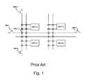
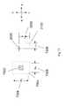
- FIG. 1is a circuit diagram illustration of a prior art
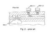
- FIG. 2is a cross-section illustration of a portion of a prior art represented by the circuit diagram of FIG. 1 ;
- FIG. 3Ais a drawing illustration of a programmable interconnect structure
- FIG. 3Bis a drawing illustration of a programmable interconnect structure
- FIG. 4Ais a drawing illustration of a programmable interconnect tile
- FIG. 4Bis a drawing illustration of a programmable interconnect of 2 ⁇ 2 tiles
- FIG. 5Ais a drawing illustration of an inverter logic cell
- FIG. 5Bis a drawing illustration of a buffer logic cell
- FIG. 5Cis a drawing illustration of a configurable strength buffer logic cell
- FIG. 5Dis a drawing illustration of a D-Flip Flop logic cell
- FIG. 6is a drawing illustration of a LUT 4 logic cell
- FIG. 6Ais a drawing illustration of a PLA logic cell
- FIG. 7is a drawing illustration of a programmable cell
- FIG. 8is a drawing illustration of a programmable device layers structure
- FIG. 8Ais a drawing illustration of a programmable device layers structure
- FIGS. 8B-8Iare drawing illustrations of the preprocessed wafers and layers and generalized layer transfer
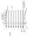
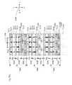
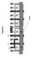
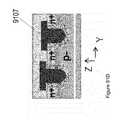
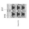
- FIGS. 9A through 9Care a drawing illustration of an IC system utilizing Through Silicon Via of a prior art
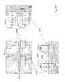
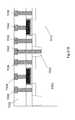
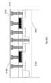
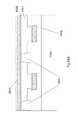
- FIG. 10Ais a drawing illustration of continuous array wafer of a prior art
- FIG. 10Bis a drawing illustration of continuous array portion of wafer of a prior art
- FIG. 10Cis a drawing illustration of continuous array portion of wafer of a prior art
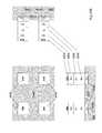
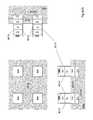
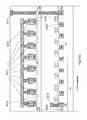
- FIGS. 11A through 11Fare a drawing illustration of one reticle site on a wafer
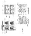
- FIGS. 12A through 12Eare a drawing illustration of Configurable system.
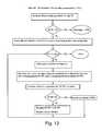
- FIG. 13a drawing illustration of a flow chart for 3D logic partitioning
- FIG. 14is a drawing illustration of a layer transfer process flow
- FIG. 15is a drawing illustration of an underlying programming circuits
- FIG. 16is a drawing illustration of an underlying isolation transistors circuits
- FIG. 17Ais a topology drawing illustration of underlying back bias circuitry
- FIG. 17Bis a drawing illustration of underlying back bias circuits
- FIG. 17Cis a drawing illustration of power control circuits
- FIG. 17Dis a drawing illustration of probe circuits
- FIG. 18is a drawing illustration of an underlying SRAM
- FIG. 19Ais a drawing illustration of an underlying I/O
- FIG. 19Bis a drawing illustration of side “cut”
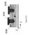
- FIG. 19Cis a drawing illustration of a 3D IC system
- FIG. 19Dis a drawing illustration of a 3D IC processor and DRAM system
- FIG. 19Eis a drawing illustration of a 3D IC processor and DRAM system
- FIG. 19Fis a drawing illustration of a custom SOI wafer used to build through-silicon connections
- FIG. 19Gis a drawing illustration of a prior art method to make through-silicon vias
- FIG. 19His a drawing illustration of a process flow for making custom SOI wafers
- FIG. 19Iis a drawing illustration of a processor-DRAM stack
- FIG. 19Jis a drawing illustration of a process flow for making custom SOI wafers
- FIG. 20is a drawing illustration of a layer transfer process flow
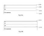
- FIG. 21Ais a drawing illustration of a pre-processed wafer used for a layer transfer
- FIG. 21Bis a drawing illustration of a pre-processed wafer ready for a layer transfer
- FIGS. 22A-22Hare drawing illustrations of formation of top planar transistors
- FIGS. 23A , 23 Bis a drawing illustration of a pre-processed wafer used for a layer transfer
- FIGS. 24A-24Fare drawing illustrations of formation of top planar transistors
- FIGS. 25A , 25 Bis a drawing illustration of a pre-processed wafer used for a layer transfer
- FIGS. 26A-26Eare drawing illustrations of formation of top planar transistors
- FIGS. 27A , 27 Bis a drawing illustration of a pre-processed wafer used for a layer transfer
- FIGS. 28A-28Eare drawing illustrations of formations of top transistors
- FIGS. 29A-29Gare drawing illustrations of formations of top planar transistors
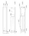
- FIG. 30is a drawing illustration of a donor wafer
- FIG. 31is a drawing illustration of a transferred layer on top of a main wafer
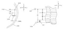
- FIG. 32is a drawing illustration of a measured alignment offset
- FIGS. 33A , 33 Bis a drawing illustration of a connection strip
- FIGS. 34A-34Eare drawing illustrations of pre-processed wafers used for a layer transfer
- FIGS. 35A-35Gare drawing illustrations of formations of top planar transistors
- FIG. 36is a drawing illustration of a tile array wafer
- FIG. 37is a drawing illustration of a programmable end device
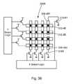
- FIG. 38is a drawing illustration of modified JTAG connections
- FIGS. 39A-39Care drawing illustration of pre-processed wafers used for vertical transistors
- FIGS. 40A-40Iare drawing illustrations of a vertical n-MOSFET top transistor
- FIG. 41is a drawing illustration of a 3D IC system with redundancy
- FIG. 42is a drawing illustration of an inverter cell
- FIGS. 43 A-Cis a drawing illustration of preparation steps for formation of a 3D cell
- FIGS. 44 A-Fis a drawing illustration of steps for formation of a 3D cell
- FIGS. 45 A-Gis a drawing illustration of steps for formation of a 3D cell
- FIGS. 46 A-Cis a drawing illustration of a layout and cross sections of a 3D inverter cell
- FIG. 47is a drawing illustration of a 2-input NOR cell
- FIGS. 48 A-Care drawing illustrations of a layout and cross sections of a 3D 2-input NOR cell
- FIGS. 49 A-Care drawing illustrations of a 3D 2-input NOR cell
- FIGS. 50 A-Dare drawing illustrations of a 3D CMOS Transmission cell
- FIGS. 51 A-Dare drawing illustrations of a 3D CMOS SRAM cell
- FIGS. 52A , 52 Bare device simulations of a junction-less transistor
- FIGS. 53 A-Eare drawing illustrations of a 3D CAM cell
- FIGS. 54 A-Care drawing illustrations of the formation of a junction-less transistor
- FIGS. 55 A-Iare drawing illustrations of the formation of a junction-less transistor
- FIGS. 56 A-Mare drawing illustrations of the formation of a junction-less transistor
- FIGS. 57A-Gare drawing illustrations of the formation of a junction-less transistor
- FIGS. 58 A-Gare drawing illustrations of the formation of a junction-less transistor
- FIG. 59is a drawing illustration of a metal interconnect stack prior art
- FIG. 60is a drawing illustration of a metal interconnect stack
- FIGS. 61 A-Iare drawing illustrations of a junction-less transistor
- FIGS. 62 A-Dare drawing illustrations of a 3D NAND2 cell
- FIGS. 63 A-Gare drawing illustrations of a 3D NAND8 cell
- FIGS. 64 A-Gare drawing illustrations of a 3D NOR8 cell
- FIGS. 65A-Care drawing illustrations of the formation of a junction-less transistor
- FIG. 66are drawing illustrations of recessed channel array transistors
- FIGS. 67A-Fare drawing illustrations of formation of recessed channel array transistors
- FIGS. 68A-Fare drawing illustrations of formation of spherical recessed channel array transistors
- FIG. 69is a drawing illustration of a donor wafer
- FIGS. 70 A, B, B- 1 , and C-Hare drawing illustrations of formation of top planar transistors
- FIG. 71is a drawing illustration of a layout for a donor wafer
- FIGS. 72 A-Fare drawing illustrations of formation of top planar transistors
- FIG. 73is a drawing illustration of a donor wafer
- FIG. 74is a drawing illustration of a measured alignment offset
- FIG. 75is a drawing illustration of a connection strip
- FIG. 76is a drawing illustration of a layout for a donor wafer
- FIG. 77is a drawing illustration of a connection strip
- FIGS. 78A , 78 Bare drawing illustrations of a layout for a donor wafer
- FIG. 79is a drawing illustration of a connection strip
- FIG. 80is a drawing illustration of a connection strip array structure
- FIGS. 81 A-Fare drawing illustrations of a formation of top planar transistors
- FIGS. 82 A-Gare drawing illustrations of a formation of top planar transistors
- FIGS. 83 A-Lare drawing illustrations of a formation of top planar transistors
- FIGS. 83 L 1 -L 4are drawing illustrations of a formation of top planar transistors
- FIGS. 84 A-Gare drawing illustrations of continuous transistor arrays
- FIGS. 85 A-Eare drawing illustrations of formation of top planar transistors
- FIG. 86Ais a drawing illustration of a 3D logic IC structured for repair
- FIG. 86Bis a drawing illustration of a 3D IC with scan chain confined to each layer
- FIG. 86Cis a drawing illustration of contact-less testing
- FIG. 87is a drawing illustration of a Flip Flop designed for repairable 3D IC logic
- FIGS. 88 A-Fare drawing illustrations of a formation of 3D DRAM
- FIGS. 89 A-Dare drawing illustrations of a formation of 3D DRAM
- FIGS. 90 A-Fare drawing illustrations of a formation of 3D DRAM
- FIGS. 91 A-Lare drawing illustrations of a formation of 3D DRAM
- FIGS. 92A-Fare drawing illustrations of a formation of 3D DRAM
- FIGS. 93 A-Dare drawing illustrations of an advanced TSV flow.
- FIGS. 94 A-Care drawing illustrations of an advanced TSV multi-connections flow.
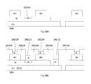
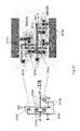
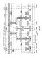
- FIG. 1illustrates a circuit diagram illustration of a prior art, where, for example, 860 - 1 to 860 - 4 are the programming transistors to program antifuse 850 - 1 , 1 .
- FIG. 2is a cross-section illustration of a portion of a prior art represented by the circuit diagram of FIG. 1 showing the programming transistor 860 - 1 built as part of the silicon substrate.
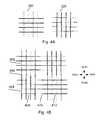
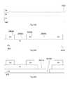
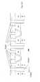
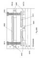
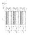
- FIG. 3Ais a drawing illustration of a programmable interconnect tile.
- 310 - 1is one of 4 horizontal metal strips, which form a band of strips.
- the typical IC todayhas many metal layers.
- the first two or three metal layerswill be used to construct the logic elements.
- metal 4 to metal 7will be used to construct the interconnection of those logic elements.
- the logic elementsare programmable, as well as the interconnects between the logic elements.
- the configurable interconnect of the current inventionis constructed from 4 metal layers or more. For example, metal 4 and 5 could be used for long strips and metal 6 and 7 would comprise short strips.
- the strips forming the programmable interconnecthave mostly the same length and are oriented in the same direction, forming a parallel band of strips as 310 - 1 , 310 - 2 , 310 - 3 and 310 - 4 .
- one bandwill comprise 10 to 40 strips.
- the strips of the following layerwill be oriented perpendicularly as illustrated in FIG. 3A , wherein strips 310 are of metal 6 and strips 308 are of metal 7 .
- the dielectric between metal 6 and metal 7comprises antifuse positions at the crossings between the strips of metal 6 and metal 7 .
- Tile 300comprises 16 such antifuses.
- 312 - 1is the antifuse at the cross of strip 310 - 4 and 308 - 4 . If activated, it will connect strip 310 - 4 with strip 308 - 4 .
- FIG. 3Awas made simplified, as the typical tile will comprise 10-40 strips in each layer and multiplicity of such tiles, which comprises the antifuse configurable interconnect structure.
- 304is one of the Y programming transistors connected to strip 310 - 1 .
- 318is one of the X programming transistors connected to strip 308 - 4 .
- 302is the Y select logic which at the programming phase allows the selection of a Y programming transistor.
- 316is the X select logic which at the programming phase allows the selection of an X programming transistor.
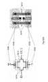
- FIG. 3Bis a drawing illustration of a programmable interconnect structure 300 B.
- 300 Bis variation of 300 A wherein some strips in the band are of a different length. Instead of strip 308 - 4 in this variation there are two shorter strips 308 - 4 B 1 and 308 - 4 B 2 . This might be useful for bringing signals in or out of the programmable interconnect structure 300 B in order to reduce the number of strips in the tile, that are dedicated to bringing signals in and out of the interconnect structure versus strips that are available to perform the routing. In such variation the programming circuit needs to be augmented to support the programming of antifuses 312 - 3 B and 312 - 4 B.
- various embodiments of the current inventionsuggest constructing the programming transistors not in the base silicon diffusion layer but rather above or below the antifuse configurable interconnect circuits.
- the programming voltage used to program the antifuseis typically significantly higher than the voltage used for the operational circuits of the device. This is part of the design of the antifuse structure so that the antifuse will not become accidentally activated.
- extra attention, design effort, and silicon resourcesmight be needed to make sure that the programming phase will not damage the operating circuits. Accordingly the incorporation of the antifuse programming transistors in the silicon substrate may require attention and extra silicon area.
- the programming circuitscould operate relatively slowly. Accordingly, a thin film transistor for the programming circuits could fit the required function and could reduce the require silicon area.
- Vacuum FETbipolar, etc.
- programming circuitscould be placed not in the base silicon but rather above or below the antifuse configurable interconnect.
- the programming transistors and the programming circuitscould be fabricated on SOI wafers which may then be bonded to the configurable logic wafer and connected to it by the use of through—silicon-via.
- An advantage of using an SOI wafer for the antifuse programming functionis that the high voltage transistors that could be built on it are very efficient and could be used for the programming circuit including support function such as the programming controller function.
- the programming circuitscould be fabricated on an older process on SOI wafers to further reduce cost. Or some other process technology and/or wafer fab located anywhere in the world.
- a common objectiveis to reduce cost for high volume production without redesign and with minimal additional mask cost.
- the use of thin-film-transistors, for the programming transistors,enables a relatively simple and direct volume cost reduction.
- a custom maskcould be used to define vias on all the locations that used to have their respective antifuse activated. Accordingly the same connection between the strips that used to be programmed is now connected by fixed vias. This may allow saving the cost associated with the fabrication of the antifuse programming layers and their programming circuits. It should be noted that there might be differences between the antifuse resistance and the mask defined via resistance.
- a conventional way to handle itis by providing the simulation models for both options so the designer could validate that the design will work properly in both cases.
- An additional objective for having the programming circuits above the antifuse layeris to achieve better circuit density. Many connections are needed to connect the programming transistors to their respective metal strips. If those connections are going upward they could reduce the circuit overhead by not blocking interconnection routes on the connection layers underneath.
- FIG. 3Ashows an interconnection structure of 4 ⁇ 4 strips
- the typical interconnection structurewill have far more strips and in many cases more than 20 ⁇ 30.
- For a 20 ⁇ 30 tile there is needed about 20+3050 programming transistors.
- one or two redistribution layersmight be needed in order to redistribute the connection within the available area and then bring those connections down, preferably aligned so to create minimum blockage as they are routed to the underlying strip 310 of the programmable interconnection structure.
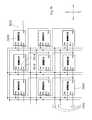
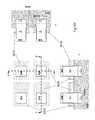
- FIG. 4Ais a drawing illustration, of a programmable interconnect tile 300 and another programmable interface tile 320 . As a higher silicon density is achieved it becomes desirable to construct the configurable interconnect in the most compact fashion.
- FIG. 4Bis a drawing illustration of a programmable interconnect of 2 ⁇ 2 tiles. It comprises checkerboard style of tiles 300 and tiles 320 which is a tile 300 rotated by 90 degrees. For a signal to travel South to North, south to north strips need to be connected with antifuses such as 406 . 406 and 410 are antifuses that are positioned at the end of a strip to allow it to connect to another strip in the same direction. The signal traveling from South to North is alternating from metal 6 to metal 7 . Once the direction needs to change, an antifuse such as 312 - 1 is used.
- the configurable interconnection structure functionmay be used to interconnect the output of logic cells to the input of logic cells to construct the desired semi-custom logic.
- the logic cellsthemselves are constructed by utilizing the first few metal layers to connect transistors that are built in the silicon substrate. Usually the metal 1 layer and metal 2 layer are used for the construction of the logic cells. Sometimes it is effective to also use metal 3 or a part of it.
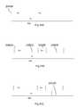
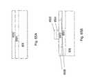
- FIG. 5Ais a drawing illustration of inverter 504 with an input 502 and an output 506 .
- An inverteris the simplest logic cell.
- the input 502 and the output 506might be connected to strips in the configurable interconnection structure.
- FIG. 5Bis a drawing illustration of a buffer 514 with an input 512 and an output 516 .
- the input 512 and the output 516might be connected to strips in the configurable interconnection structure.
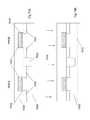
- FIG. 5Cis a drawing illustration of a configurable strength buffer 524 with an input 522 and an output 526 .
- the input 522 and the output 526might be connected to strips in the configurable interconnection structure.
- 524is configurable by means of antifuses 528 - 1 , 528 - 2 and 528 - 3 constructing an antifuse configurable drive cell.
- FIG. 5Dis a drawing illustration of D-Flip Flop 534 with inputs 532 - 2 , and output 536 with control inputs 532 - 1 , 532 - 3 , 532 - 4 and 532 - 5 .
- the control signalscould be connected to the configurable interconnects or to local or global control signals.
- FIG. 6is a drawing illustration of a LUT 4 .
- LUT 4 604is a well-known logic element in the FPGA art called a 16 bit Look-Up-Table or in short LUT 4 . It has 4 inputs 602 - 1 , 602 - 2 , 602 - 3 and 602 - 4 . It has an output 606 .
- a LUT 4can be programmed to perform any logic function of 4 inputs or less.
- the LUT function of FIG. 6may be implemented by 32 antifuses such as 608 - 1 . 604 - 5 is a two to one multiplexer.
- the common way to implement a LUT 4 in FPGAis by using 16 SRAM bit-cells and 15 multiplexers.
- FIG. 6demonstrates an antifuse configurable look-up-table implementation of a LUT 4 by 32 antifuses and 7 multiplexers.
- the programmable cell of FIG. 6may comprise additional inputs 602 - 6 , 602 - 7 with additional 8 antifuse for each input to allow some functionality in addition to just LUT 4 .
- FIG. 6Ais a drawing illustration of a PLA logic cell 6 A 00 . This used to be the most popular programmable logic primitive until LUT logic took the leadership. Other acronyms used for this type of logic are PLD and PAL.
- 6 A 01is one of the antifuses that enables the selection of the signal fed to the multi-input AND 6 A 14 . In this drawing any cross between vertical line and horizontal line comprises an antifuse to allow the connection to be made according to the desired end function.
- the large AND cell 6 A 14constructs the product term by performing the AND function on the selection of inputs 6 A 02 or their inverted replicas.
- a multi-input OR 6 A 15performs the OR function on a selection of those product terms to construct an output 6 A 06 .
- FIG. 6Aillustrates an antifuse configurable PLA logic.
- FIG. 5 , FIG. 6 and FIG. 6Aare just representatives. There exist many options for construction of programmable logic fabric including additional logic cells such as AND, MUX and many others, and variations on those cells. Also, in the construction of the logic fabric there might be variation with respect to which of their inputs and outputs are connected by the configurable interconnect fabric and which are connected directly in a non-configurable way.
- FIG. 7is a drawing illustration of a programmable cell 700 .
- a programmable fabricBy tiling such cells a programmable fabric is constructed. The tiling could be of the same cell being repeated over and over to form a homogenous fabric. Alternatively, a blend of different cells could be tiled for heterogeneous fabric.
- the logic cell 700could be any of those presented in FIGS. 5 and 6 , a mix and match of them or other primitives as discussed before.
- the logic cell 710 inputs 702 and output 706are connected to the configurable interconnection fabric 720 with input and output strips 708 with associated antifuses 701 .
- the short interconnects 722are comprising metal strips that are the length of the tile, they comprise horizontal strips 722 H, on one metal layer and vertical strips 722 V on another layer, with antifuse 701 HV in the cross between them, to allow selectively connecting horizontal strip to vertical strip.
- the connection of a horizontal strip to another horizontal stripis with antifuse 701 HH that functions like antifuse 410 of FIG. 4 .
- the connection of a vertical strip to another vertical stripis with antifuse 701 VV that functions like fuse 406 of FIG. 4 .
- the long horizontal strips 724are used to route signals that travel a longer distance, usually the length of 8 or more tiles.
- FIG. 7illustrates the programmable cell 700 as a two dimensional illustration.
- the logic cell 710utilizes the base silicon with Metal 1 , Metal 2 , and some times Metal 3 .
- the programmable interconnect fabric including the associated antifuseswill be constructed on top of it.
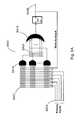
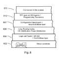
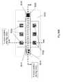
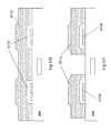
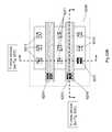
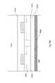
- FIG. 8is a drawing illustration of a programmable device layers structure according to an alternative of the current invention.
- the firstis designated to configure the logic terrain and, in some cases, to also configure the logic clock distribution.
- the first antifuse layercould also be used to manage some of the power distribution to save power by not providing power to unused circuits.
- This layercould also be used to connect some of the long routing tracks and/or connections to the inputs and outputs of the logic cells.
- the device fabrication of the example shown in FIG. 8starts with the semiconductor substrate 802 comprising the transistors used for the logic cells and also the first antifuse layer programming transistors. Then comes layers 804 comprising Metal 1 , dielectric, Metal 2 , and sometimes Metal 3 . These layers are used to construct the logic cells and often I/O and other analog cells.
- a plurality of first antifusesare incorporated in the isolation layer between metal 1 and metal 2 or in the isolation layer between metal 2 and metal 3 and their programming transistors could be embedded in the silicon substrate 802 being underneath the first antifuses.
- These first antifusescould be used to program logic cells such as 520 , 600 and 700 and to connect individual cells to construct larger logic functions. These first antifuses could also be used to configure the logic clock distribution.
- the first antifuse layercould also be used to manage some of the power distribution to save power by not providing power to unused circuits. This layer could also be used to connect some of the long routing tracks and/or one or more connections to the inputs and outputs of the cells.
- the following few layers 806could comprise long interconnection tracks for power distribution and clock networks, or a portion of these, in addition to what was fabricated in the first few layers 804 .
- the following few layers 807could comprise the antifuse configurable interconnection fabric. It might be called the short interconnection fabric, too. If metal 6 and metal 7 are used for the strips of this configurable interconnection fabric then the second antifuse may be embedded in the dielectric layer between metal 6 and metal 7 .
- the programming transistors and the other parts of the programming circuitcould be fabricated afterward and be on top of the configurable interconnection fabric 810 .
- the programming elementcould be a thin film transistor or other alternatives for over oxide transistors as was mentioned previously.
- the antifuse programming transistorsare placed over the antifuse layer, which may thereby enable the configurable interconnect 808 or 804 . It should be noted that in some cases it might be useful to construct part of the control logic for the second antifuse programming circuits, in the base layers 802 and 804 .
- connection to the outside 812could be pads for wire bonding, soldering balls for flip chip, optical, or other connection structures such as those required for TSV.
- the antifuse programmable interconnect structurecould be designed for multiple use.
- the same structurecould be used as a part of the interconnection fabric, or as a part of the PLA logic cell, or as part of a Read Only Memory (ROM) function.
- ROMRead Only Memory
- FPGA productit might be desirable to have an element that could be used for multiple purposes. Having resources that could be used for multiple functions could increase the utility of the FPGA device.
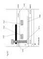
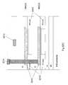
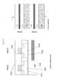
- FIG. 8Ais a drawing illustration of a programmable device layers structure according to another alternative of the current invention.
- this alternativethere is additional circuit 814 connected by contact connection 816 to the first antifuse layer 804 .
- This underlying deviceis providing the programming transistor for the first antifuse layer 804 .
- the programmable device substrate diffusion layer 816does not suffer the cost penalty of the programming transistors required for the first antifuse layer 804 .
- the programming connection of the first antifuse layer 804will be directed downward to connect to the underlying programming device 814 while the programming connection to the second antifuse layer 807 will be directed upward to connect to the programming circuits 810 . This could provide less congestion of the circuit internal interconnection routes.
- preprocessed wafer or layermay be generic and reference number 808 when used in a drawing figure to illustrate an embodiment of the present invention may represent many different preprocessed wafer or layer types including but not limited to underlying prefabricated layers, a lower layer interconnect wiring, a base layer, a substrate layer, a processed house wafer, an acceptor wafer, a logic house wafer, an acceptor wafer house, preprocessed circuitry, a preprocessed circuitry acceptor wafer, a base wafer layer, a lower layer, an underlying main wafer, a foundation layer, an attic layer, or a house wafer.
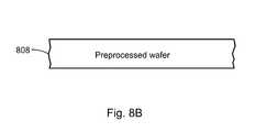
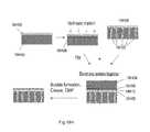
- FIG. 8Bis a drawing illustration of a generalized preprocessed wafer or layer 808 .
- the wafer or layer 808may have preprocessed circuitry, such as, for example, logic circuitry, microprocessors, circuitry comprising transistors of various types, and other types of digital or analog circuitry including, but not limited to, the various embodiments described herein.
- Preprocessed wafer or layer 808may have preprocessed metal interconnects.
- the preprocessed metal interconnectsmay be designed and prepared for layer transfer and electrical coupling from preprocessed wafer or layer 808 to the layer or layers to be transferred.
- FIG. 8Cis a drawing illustration of a generalized transfer layer 809 prior to being attached to preprocessed wafer or layer 808 .
- Transfer layer 809may be attached to a carrier wafer or substrate during layer transfer.
- Transfer layer 809may have metal interconnects designed and prepared for layer transfer and electrical coupling to preprocessed wafer or layer 808 .
- FIG. 8Dis a drawing illustration of a preprocessed wafer or layer 808 A created by the layer transfer of transfer layer 809 on top of preprocessed wafer or layer 808 .
- the top of preprocessed wafer or layer 808 Amay be further processed with metal interconnects designed and prepared for layer transfer and electrical coupling from preprocessed wafer or layer 808 A to the next layer or layers to be transferred.
- FIG. 8Eis a drawing illustration of a generalized transfer layer 809 A prior to being attached to preprocessed wafer or layer 808 A.
- Transfer layer 809 Amay be attached to a carrier wafer or substrate during layer transfer.
- Transfer layer 809 Amay have metal interconnects designed and prepared for layer transfer and electrical coupling to preprocessed wafer or layer 808 A.
- FIG. 8Fis a drawing illustration of a preprocessed wafer or layer 808 B created by the layer transfer of transfer layer 809 A on top of preprocessed wafer or layer 808 A.
- the top of preprocessed wafer or layer 808 Bmay be further processed with metal interconnects designed and prepared for layer transfer and electrical coupling from preprocessed wafer or layer 808 B to the next layer or layers to be transferred.
- FIG. 8Gis a drawing illustration of a generalized transfer layer 809 B prior to being attached to preprocessed wafer or layer 808 B.
- Transfer layer 809 Bmay be attached to a carrier wafer or substrate during layer transfer.
- Transfer layer 809 Bmay have metal interconnects designed and prepared for layer transfer and electrical coupling to preprocessed wafer or layer 808 B.
- FIG. 8His a drawing illustration of preprocessed wafer layer 808 C created by the layer transfer of transfer layer 809 B on top of preprocessed wafer or layer 808 B.
- the top of preprocessed wafer or layer 808 Cmay be further processed with metal interconnect designed and prepared for layer transfer and electrical coupling from preprocessed wafer or layer 808 C to the next layer or layers to be transferred.
- FIG. 8Iis a drawing illustration of preprocessed wafer or layer 808 C, a 3D IC stack, which may comprise transferred layers 809 A and 809 B on top of the original preprocessed wafer or layer 808 .
- Transferred layers 809 A and 809 B and the original preprocessed wafer or layer 808may comprise transistors of one or more types in one or more layers, metallization in one or more layers, interconnections to and between layers above and below, and interconnections within the layer.
- the transistorsmay be of various types that may be different from layer to layer or within the same layer.
- the transistorsmay be in various organized patterns.
- the transistorsmay be in various pattern repeats or bands.
- the transistorsmay be in multiple layers involved in the transfer layer.
- Transferred layers 809 A and 809 B and the original preprocessed wafer or layer 808may further comprise semiconductor devices such as resistors and capacitors and inductors, one or more programmable interconnects, memory structures and devices, sensors, radio frequency devices, or optical interconnect with associated transceivers.
- This layer transfer processcan be repeated many times, thereby creating preprocessed wafers comprising many different transfer layers which, when combined, can then become preprocessed wafers or layers for future transfers.
- This layer transfer processmay be sufficiently flexible and preprocessed wafers and transfer layers, if properly prepared, can be flipped over and processed on either side with further transfers in either direction as a matter of design choice.
- FIGS. 8 through 8Iare exemplary only and are not drawn to scale.
- the preprocessed wafer or layer 808may act as a base or substrate layer in a wafer transfer flow, or as a preprocessed or partially preprocessed circuitry acceptor wafer in a wafer transfer process flow.
- the inventionis to be limited only by the appended claims.
- the “SmartCut” processis a well understood technology used for fabrication of SOI wafers.
- the “SmartCut” processtogether with wafer bonding technology, enables a “Layer Transfer” whereby a thin layer of a silicon wafer is transferred from one wafer to another wafer.
- the “Layer Transfer”could be done at less than 400° C. and the resultant transferred layer could be even less than 100 nm thick.
- SoitecCrops, France
- SiGen—Silicon Genesis CorporationSan Jose, Calif.
- a room temperature wafer bonding process utilizing ion-beam preparation of the wafer surfaces in a vacuumhas been recently demonstrated by Mitsubishi Heavy Industries Ltd., Tokyo, Japan. This process allows room temperature layer transfer.
- the IBM's layer transfer methodemploys a SOI technology and utilizes glass handle wafers.
- the donor circuitmay be high-temperature processed on an SOI wafer, temporarily bonded to a borosilicate glass handle wafer, backside thinned by chemical mechanical polishing of the silicon and then the Buried Oxide (BOX) is selectively etched off.
- BOXBuried Oxide
- ELOepitaxial liftoff
- the to-be-transferred layer of GaAs or siliconmay be adhesively ‘rolled’ up on a cylinder or removed from the substrate by utilizing a flexible carrier, such as, for example, black wax, to bow up the to-be-transferred layer structure when the selective etch, such as, for example, diluted Hydrofluoric (HF) Acid, etches the exposed release layer, such as, for example, silicon oxide in SOI or AlAs. After liftoff, the transferred layer is then aligned and bonded to the desired acceptor substrate or wafer.
- a flexible carriersuch as, for example, black wax
- ELTRANepitaxial Layer TRaNsfer from porous silicon.
- ELTRANmay be utilized.
- the Electrochemical Society Meeting abstract No. 438 from year 2000 and the JSAP International July 2001 papershow a seed wafer being anodized in an HF/ethanol solution to create pores in the top layer of silicon, the pores are treated with a low temperature oxidation and then high temperature hydrogen annealed to seal the pores.
- Epitaxial siliconmay then be deposited on top of the porous silicon and then oxidized to form the SOI BOX.
- the seed wafermay be bonded to a handle wafer and the seed wafer may be split off by high pressure water directed at the porous silicon layer.
- the porous siliconmay then be selectively etched off leaving a uniform silicon layer.
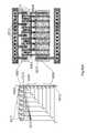
- FIG. 14is a drawing illustration of a layer transfer process flow.
- “Layer-Transfer”is used for construction of the underlying circuitry 814 .
- 1402is a wafer that was processed to construct the underlying circuitry.
- the wafer 1402could be of the most advanced process or more likely a few generations behind. It could comprise the programming circuits 814 and other useful structures.
- An oxide layer 1412is then deposited on top of the wafer 1402 and then is polished for better planarization and surface preparation.
- a donor wafer 1406is then brought in to be bonded to 1402 .
- the surfaces of both donor wafer 1406 and wafer 1402may have a plasma pretreatment to enhance the bond strength.
- the donor wafer 1406is pre-prepared for “SmartCut” by an ion implant of an atomic species, such as H+ ions, at the desired depth to prepare the SmartCut line 1408 .
- a SmartCut stepis performed to cleave and remove the top portion 1414 of the donor wafer 1406 along the cut layer 1408 .
- the resultis a 3D wafer 1410 which comprises wafer 1402 with an added layer 1404 of crystallized silicon. Layer 1404 could be quite thin at the range of 50-200 nm as desired.
- the described flowis called “layer transfer”. Layer transfer is commonly utilized in the fabrication of SOI—Silicon On Insulator—wafers. For SOI wafers the upper surface is oxidized so that after “layer transfer” a buried oxide—BOX—provides isolation between the top thin crystallized silicon layer and the bulk of the wafer.
- a “layer transfer” processis used to bond a thin crystallized silicon layer 1404 on top of the preprocessed wafer 1402 , a standard process could ensue to construct the rest of the desired circuits as is illustrated in FIG. 8A , starting with layer 802 on the transferred layer 1404 .
- the lithography stepwill use alignment marks on wafer 1402 so the following circuits 802 and 816 and so forth could be properly connected to the underlying circuits 814 .
- An aspect that should be accounted foris the high temperature that would be needed for the processing of circuits 802 .
- the pre-processed circuits on wafer 1402would need to withstand this high temperature needed for the activation of the semiconductor transistors 802 fabricated on the 1404 layer.
- Those foundation circuits on wafer 1402will comprise transistors and local interconnects of poly-silicon and some other type of interconnection that could withstand high temperature such as tungsten.
- An advantage of using layer transfer for the construction of the underlying circuitsis having the layer transferred 1404 be very thin which enables the through silicon via connections 816 to have low aspect ratios and be more like normal contacts, which could be made very small and with minimum area penalty.
- the thin transferred layeralso allows conventional direct thru-layer alignment techniques to be performed, thus increasing the density of silicon via connections 816 .
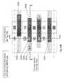
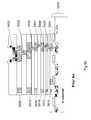
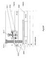
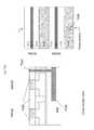
- FIG. 15is a drawing illustration of an underlying programming circuit.
- Programming Transistors 1501 and 1502are pre-fabricated on the foundation wafer 1402 and then the programmable logic circuits and the antifuse 1504 are built on the transferred layer 1404 .
- the programming connections 1506 , 1508are connected to the programming transistors by contact holes through layer 1404 as illustrated in FIG. 8A by 816 .
- the programming transistorsare designed to withstand the relatively higher programming voltage required for the antifuse 1504 programming.
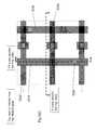
- FIG. 16is a drawing illustration of an underlying isolation transistor circuit.
- the higher voltage used to program the antifuse 1604might damage the logic transistors 1606 , 1608 .
- isolation transistors 1601 , 1602which are designed to withstand higher voltage, are used.
- the higher programming voltageis only used at the programming phase at which time the isolation transistors are turned off by the control circuit 1603 .
- the underlying wafer 1402could also be used to carry the isolation transistors. Having the relatively large programming transistors and isolation transistor on the foundation silicon 1402 allows far better use of the primary silicon 802 ( 1404 ). Usually the primary silicon will be built in an advanced process to provide high density and performance.
- the foundation siliconcould be built in a less advanced process to reduce costs and support the higher voltage transistors. It could also be built with other than CMOS transistors such as Double Diffused Metal Oxide Semiconductor (DMOS) or bi-polar junction transistors when such is advantageous for the programming and the isolation function.
- CMOS transistorssuch as Double Diffused Metal Oxide Semiconductor (DMOS) or bi-polar junction transistors when such is advantageous for the programming and the isolation function.
- DMOSDouble Diffused Metal Oxide Semiconductor
- bi-polar junction transistorswhen such is advantageous for the programming and the isolation function.
- protection diodes for the gate inputthat are called Antennas.
- Such protection diodescould be also effectively integrated in the foundation alongside the input related Isolation Transistors.
- the isolation transistors 1601 , 1602would provide the protection for the antenna effect so no additional diodes would be needed.
- An additional alternative embodiment of the inventionis where the foundation layer 1402 is pre-processed to carry a plurality of back bias voltage generators.
- a known challenge in advanced semiconductor logic devicesis die-to-die and within-a-die parameter variations. Various sites within the die might have different electrical characteristics due to dopant variations and such. The most critical of these parameters that affect the variation is the threshold voltage of the transistor. Threshold voltage variability across the die is mainly due to channel dopant, gate dielectric, and critical dimension variability. This variation becomes profound in sub 45 nm node devices. The usual implication is that the design should be done for the worst case, resulting in a quite significant performance penalty. Alternatively complete new designs of devices are being proposed to solve this variability problem with significant uncertainty in yield and cost. A possible solution is to use localized back bias to drive upward the performance of the worst zones and allow better overall performance with minimal additional power. The foundation-located back bias could also be used to minimize leakage due to process variation.
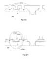
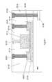
- FIG. 17Ais a topology drawing illustration of back bias circuitry.
- the foundation layer 1402carries back bias circuits 1711 to allow enhancing the performance of some of the zones 1710 on the primary device which otherwise will have lower performance.
- FIG. 17Bis a drawing illustration of back bias circuits.
- a back bias level control circuit 1720is controlling the oscillators 1727 and 1729 to drive the voltage generators 1721 .
- the negative voltage generator 1725will generate the desired negative bias which will be connected to the primary circuit by connection 1723 to back bias the N-channel Metal-Oxide-Semiconductor (NMOS) transistors 1732 on the primary silicon 1404 .
- the positive voltage generator 1726will generate the desired negative bias which will be connected to the primary circuit by connection 1724 to back bias the P-channel Metal-Oxide-Semiconductor (PMOS) transistors 1724 on the primary silicon 1404 .
- the setting of the proper back bias level per zonewill be done in the initiation phase.
- a non volatile memorywill be used to store the per zone back bias voltage level so the device could be properly initialized at power up.
- a dynamic schemecould be used where different back bias level(s) are used in different operating modes of the device. Having the back bias circuitry in the foundation allows better utilization of the primary device silicon resources and less distortion for the logic operation on the primary device.
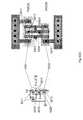
- FIG. 17Cillustrates an alternative circuit function that may fit well in the “Foundation.”
- a power control circuit cell 17 C 02may be constructed in the Foundation.
- Such power control 17 C 02may have its own higher voltage supply and control or regulate supply voltage for sections 17 C 10 and 17 C 08 in the “Primary” device.
- the controlmay come from the primary device 17 C 16 and be managed by control circuit 17 C 04 in the Foundation.
- FIG. 17Dillustrates an alternative circuit function that may fit well in the “Foundation.”
- Probe circuitshave been used in the prior art sharing the same transistor layer as the primary circuit.
- FIG. 17Dillustrates a probe circuit constructed in the Foundation underneath the active circuits in the primary layer.
- FIG. 17Dillustrates that the connections are made to the sequential active circuit elements 17 D 02 . Those connections are routed to the Foundation through interconnect lines 17 D 06 where high impedance probe circuits 17 D 08 will be used to sense the sequential element output.
- a selector circuit 17 D 12allows one or more of those sequential outputs to be routed out through one or more buffers 17 D 16 which may be controlled by signals from the Primary circuit to supply the drive of the sequential output signal to the probed signal output 17 D 14 for debugging or testing.
- buffers 17 D 16which may be controlled by signals from the Primary circuit to supply the drive of the sequential output signal to the probed signal output 17 D 14 for debugging or testing.
- Persons of ordinary skill in the artwill appreciate that other configurations are possible like, for example, having multiple groups of probe circuitry 17 D 08 , multiple probe output signals 17 D 14 , and controlling buffers 17 D 16 with signals not originating in the primary circuit.
- the foundation substrate 1402could additionally carry SRAM cells as illustrated in FIG. 18 .
- the SRAM cells 1802 pre-fabricated on the underlying substrate 1402could be connected 1812 to the primary logic circuit 1806 , 1808 built on 1404 .
- the layers built on 1404could be aligned to the pre-fabricated structure on the underlying substrate 1402 so that the logic cells could be properly connected to the underlying RAM cells.
- FIG. 19Ais a drawing illustration of an underlying I/O.
- the foundation 1402could also be preprocessed to carry the I/O circuits or part of it, such as the relatively large transistors of the output drive 1912 . Additionally TSV in the foundation could be used to bring the I/O connection 1914 all the way to the back side of the foundation.
- FIG. 19Bis a drawing illustration of a side “cut” of an integrated device of the present invention.
- the Output Driveris illustrated by PMOS and NMOS output transistors 19 B 06 coupled through TSV 19 B 10 to connect to a backside pad or pad bump 19 B 08 .
- the connection material used in the foundation 1402can be selected to withstand the temperature of the following process constructing the full device on 1404 as illustrated in FIG. 8 A— 802 , 804 , 806 , 807 , 810 , 812 , such as tungsten.
- the foundationcould also carry the input protection circuit 1916 connecting the pad 19 B 08 to the input logic 1920 in the primary circuits
- An additional embodiment of the present inventionmay be to use TSVs in the foundation such as TSV 19 B 10 to connect between wafers to form 3D Integrated Systems.
- each TSVtakes a relatively large area, typically a few square microns.
- the overall cost of the required area for these TSVsmight be high if the use of that area for high density transistors is precluded.
- Pre-processing these TSVs on the donor wafer on a relatively older process linewill significantly reduce the effective costs of the 3D TSV connections.
- the connection 1924 to the primary silicon circuitry 1920could be then made at the minimum contact size of few tens of square nanometers, which is two orders of magnitude lower than the few square microns required by the TSVs.
- FIG. 19Bis for illustration only and is not drawn to scale. Such skilled persons will understand there are many alternate embodiments and component arrangements that could be constructed using the inventive principles shown and that FIG. 19B is not limiting in any way.
- FIG. 19Cdemonstrates a 3D system comprising three dice 19 C 10 , 19 C 20 and 19 C 30 coupled together with TSVs 19 C 12 , 19 C 22 and 19 C 32 similar to TSV 19 B 10 as described in association with FIG. 19A .
- the stack of three diceutilize TSV in the Foundations 19 C 12 , 19 C 22 , and 19 C 32 for the 3D interconnect may allow for minimum effect or silicon area loss of the Primary silicon 19 C 14 , 19 C 24 and 19 C 34 connected to their respective Foundations with minimum size via connections.
- the three die stacksmay be connected to a PC Board using bumps 19 C 40 connected to the bottom die TSVs 19 C 32 .
- FIG. 19Cis for illustration only and is not drawn to scale.
- FIG. 19Cis not limiting in any way.
- a die stackcould be placed in a package using flip chip bonding or the bumps 19 C 40 could be replaced with bond pads and the part flipped over and bonded in a conventional package with bond wires.
- FIG. 19Dillustrates a 3D IC processor and DRAM system.
- a well known problem in the computing industryis known as the “memory wall” and relates to the speed the processor can access the DRAM.
- the prior art proposed solutionwas to connect a DRAM stack using TSV directly on top of the processor and use a heat spreader attached to the processor back to remove the processor heat. But in order to do so, a special via needs to go “through DRAM” so that the processor I/Os and power could be connected. Having many processor-related ‘through-DRAM vias” leads to a few severe disadvantages. First, it reduces the usable silicon area of the DRAM by a few percent. Second, it increases the power overhead by a few percent.
- FIG. 19Dillustrates one solution to mitigate the above mentioned disadvantages by having a foundation with TSVs as illustrated in FIGS. 19B and 19 C.
- the use of the foundation and primary structuremay enable the connections of the processor without going through the DRAM.
- the processor I/Os and powermay be coupled from the face-down microprocessor active area 19 D 14 —the primary layer, by vias 19 D 08 through heat spreader substrate 19 D 04 to an interposer 19 D 06 .
- a heat spreader 19 D 12 , the heat spreader substrate 19 D 04 , and heat sink 19 D 02are used to spread the heat generated on the processor active area 19 D 14 .
- TSVs 19 D 22 through the Foundation 19 D 16are used for the connection of the DRAM stack 19 D 24 .
- the DRAM stackcomprises multiple thinned DRAM 19 D 18 interconnected by TSV 19 D 20 . Accordingly the DRAM stack does not need to pass through the processor I/O and power planes and could be designed and produced independent of the processor design and layout.
- the DRAM chip 19 D 18 that is closest to the Foundation 19 D 16may be designed to connect to the Foundation TSVs 19 D 22 , or a separate ReDistribution Layer (or RDL, not shown) may be added in between, or the Foundation 19 D 16 could serve that function with preprocessed high temperature interconnect layers, such as Tungsten, as described previously. And the processor's active area is not compromised by having TSVs through it as those are done in the Foundation 19 D 16 .
- Foundation vias 19 D 22could be used to pass the processor I/O and power to the substrate 19 D 04 and to the interposer 19 D 06 while the DRAM stack would be coupled directly to the processor active area 19 D 14 .
- Persons of ordinary skill in the artwill appreciate that many more combinations are possible within the scope of the disclosed invention.
- FIG. 19Eillustrates another embodiment of the present invention wherein the DRAM stack 19 D 24 may be coupled by wire bonds 19 E 24 to an RDL (ReDistribution Layer) 19 E 26 that couples the DRAM to the Foundation vias 19 D 22 , and thus couples them to the face-down processor 19 D 14 .
- RDLDistribution Layer
- NuVias 19 F 00may be processed by the wafer supplier.
- NuVias 19 F 00may be conventional TSVs that may be 1 micron or larger in diameter and may be preprocessed by an SOI wafer vendor. This is illustrated in FIG. 19F with handle wafer 19 F 02 and Buried Oxide BOX 19 F 01 .
- the handle wafer 19 F 02may typically be many hundreds of microns thick, and the BOX 19 F 01 may typically be a few hundred nanometers thick.
- the Integrated Device Manufacturer (IDM) or foundrythen processes NuContacts 19 F 03 to connect to the NuVias 19 F 00 .
- IDMIntegrated Device Manufacturer
- NuContactsmay be conventionally dimensioned contacts etched thru the thin silicon 19 F 05 and the BOX 19 F 01 of the SOI and filled with metal.
- the NuContact diameter D NuContact 19 F 04 , in FIG. 19Fmay then be processed into the tens of nanometer range.
- the prior art of construction with bulk silicon wafers 19 G 00 as illustrated in FIG. 19Gtypically has a TSV diameter, D TSV — prior — art 19 G 02 , in the micron range.
- the reduced dimension of NuContact D NuContact 19 F 04 in FIG. 19Fmay have important implications for semiconductor designers.
- the use of NuContactsmay provide reduced die size penalty of through-silicon connections, reduced handling of very thin silicon wafers, and reduced design complexity.
- the arrangement of TSVs in custom SOI waferscan be based on a high-volume integrated device manufacturer (IDM) or foundry's request, or be based on a commonly agreed industry standard.
- IDMintegrated device manufacturer
- a process flow as illustrated in FIG. 19Hmay be utilized to manufacture these custom SOI wafers. Such a flow may be used by a wafer supplier.
- a silicon donor wafer 19 H 04is taken and its surface 19 H 05 may be oxidized.
- An atomic species, such as, for example, hydrogen,may then be implanted at a certain depth 19 H 06 .
- Oxide-to-oxide bonding as described in other embodimentsmay then be used to bond this wafer with an acceptor wafer 19 H 08 having pre-processed NuVias 19 H 07 .
- the NuVias 19 H 07may be constructed with a conductive material, such as tungsten or doped silicon, which can withstand high-temperature processing.
- An insulating barriersuch as, for example, silicon oxide, may be utilized to electrically isolate the NuVia 19 H 07 from the silicon of the acceptor wafer 19 H 08 .
- the wafer suppliermay construct NuVias 19 H 07 with silicon oxide.
- the integrated device manufacturer or foundryetches out this oxide after the high-temperature (more than 400° C.) transistor fabrication is complete and may replace this oxide with a metal such as copper or aluminum. This process may allow a low-melting point, but highly conductive metal, like copper to be used.
- a portion 19 H 10 of the donor silicon wafer 19 H 04may be cleaved at 19 H 06 and then chemically mechanically polished as described in other embodiments.
- FIG. 19Jdepicts another technique to manufacture custom SOI wafers.
- a standard SOI wafer with substrate 19 J 01 , box 19 F 01 , and top silicon layer 19 J 02may be taken and NuVias 19 F 00 may be formed from the back-side up to the oxide layer.
- This techniquemight require a thicker buried oxide 19 F 01 than a standard SOI process.
- FIG. 19Idepicts how a custom SOI wafer may be used for 3D stacking of a processor 19 I 09 and a DRAM 19 I 10 .
- a processor's power distribution and I/O connectionshave to pass from the substrate 19 I 12 , go through the DRAM 19 I 10 and then connect onto the processor 19 I 09 .
- the above described technique in FIG. 19Fmay result in a small contact area on the DRAM active silicon, which is very convenient for this processor-DRAM stacking application.
- the transistor area lost on the DRAM die due to the through-silicon connection 19 I 13 and 19 I 14is very small due to the tens of nanometer diameter of NuContact 19 I 13 in the active DRAM silicon.
- the foundation substrate 1402could additionally carry re-drive cells (often called buffers).
- Re-drive cellsare common in the industry for signals which is routed over a relatively long path. As the routing has a severe resistance and capacitance penalty it is helpful to insert re-drive circuits along the path to avoid a severe degradation of signal timing and shape.
- An advantage of having re-drivers in the foundation 1402is that these re-drivers could be constructed from transistors who could withstand the programming voltage. Otherwise isolation transistors such as 1601 and 1602 or other isolation scheme may be used at the logic cell input and output.
- FIG. 8Ais a cut illustration of a programmable device, with two antifuse layers.
- the programming transistors for the first one 804could be prefabricated on 814 , and then, utilizing “smart-cut”, a single crystal silicon layer 1404 is transferred on which the primary programmable logic 802 is fabricated with advanced logic transistors and other circuits. Then multi-metal layers are fabricated including a lower layer of antifuses 804 , interconnection layers 806 and second antifuse layer with its configurable interconnects 807 .
- the programming transistors 810could be fabricated also utilizing a second “smart-cut” layer transfer.
- FIG. 20is a drawing illustration of the second layer transfer process flow.
- the primary processed wafer 2002comprises all the prior layers- 814 , 802 , 804 , 806 , and 807 .
- An oxide layer 2012is then deposited on top of the wafer 2002 and then polished for better planarization and surface preparation.
- a donor wafer 2006(or cleavable wafer as labeled in the drawing) is then brought in to be bonded to 2002 .
- the donor wafer 2006is pre processed to comprise the semiconductor layers 2019 which will be later used to construct the top layer of programming transistors 810 as an alternative to the TFT transistors.
- the donor wafer 2006is also prepared for “SmartCut” by ion implant of an atomic species, such as H+, at the desired depth to prepare the SmartCut line 2008 .
- a SmartCut stepis performed to pull out the top portion 2014 of the donor wafer 2006 along the cut layer 2008 .
- This donor wafermay now also be processed and reused for more layer transfers.
- the resultis a 3D wafer 2010 which comprises wafer 2002 with an added layer 2004 of single crystal silicon pre-processed to carry additional semiconductor layers.
- the transferred slice 2004could be quite thin at the range of 10-200 nm as desired.
- Utilizing “SmartCut” layer transferprovides single crystal semiconductors layer on top of a pre-processed wafer without heating the pre-processed wafer to more than 400° C.
- top transistorsprecisely aligned to the underlying pre-fabricated layers such as pre-processed wafer or layer 808 , utilizing “SmartCut” layer transfer and not exceeding the temperature limit of the underlying pre-fabricated structure.
- layer transferis less than 200 nm thick, then the transistors defined on it could be aligned precisely to the top metal layer of the pre-processed wafer or layer 808 as required and those transistors have less than 40 nm misalignment.
- One alternative methodis to have a thin layer transfer of single crystal silicon which will be used for epitaxial Ge crystal growth using the transferred layer as the seed for the germanium.
- Another alternative methodis to use the thin layer transfer of crystallized silicon for epitaxial growth of Ge x Si 1-x .
- the percent Ge in Silicon of such layerwould be determined by the transistor specifications of the circuitry.
- Prior arthave presented approaches whereby the base silicon is used to epi-crystallize the germanium on top of the oxide by using holes in the oxide to drive seeding from the underlying silicon crystal. However, it is very hard to do such on top of multiple interconnection layers. By using layer transfer we can have the silicon crystal on top and make it relatively easy to seed and epi-crystallize an overlying germanium layer.
- Amorphous germaniumcould be conformally deposited by CVD at 300° C. and pattern aligned to the underlying layer, such as the pre-processed wafer or layer 808 , and then encapsulated by a low temperature oxide.
- a short ⁇ s-duration heat pulsemelts the Ge layer while keeping the underlying structure below 400° C.
- the Ge/Si interfacewill start the epi-growth to crystallize the germanium or Ge x Si 1-x layer. Then implants are made to form Ge transistors and activated by laser pulses without damaging the underlying structure taking advantage of the low melting temperature of germanium.
- FIG. 21Ais a drawing illustration of a pre-processed wafer used for a layer transfer.
- a lightly doped P-type wafer (P ⁇ wafer) 2102may be processed to have a “buried” layer of highly doped N-type silicon (N+) 2104 , by implant and activation, or by shallow N+ implant and diffusion followed by a P ⁇ epi growth (epitaxial growth) 2106 .
- N+highly doped N-type silicon
- P ⁇ epi growthepi growth
- 21Bis a drawing illustration of the pre-processed wafer made ready for a layer transfer by an implant of an atomic species, such as H+, preparing the SmartCut “cleaving plane” 2110 in the lower part of the N+ region and an oxide deposition or growth 2112 in preparation for oxide to oxide bonding.
- a layer-transfer-flowshould be performed to transfer the pre-processed single crystal P ⁇ silicon with N+ layer, on top of pre-processed wafer or layer 808 .
- the top of pre-processed wafer or layer 808may be prepared for bonding by deposition of an oxide, or surface treatments, or both.
- Persons of ordinary skill in the artwill appreciate that the processing methods presented above are illustrative only and that other embodiments of the inventive principles described herein are possible and thus the scope if the invention is only limited by the appended claims.
- FIGS. 22A-22Hare drawing illustrations of the formation of planar top source extension transistors.
- FIG. 22Aillustrates the layer transferred on top of preprocessed wafer or layer 808 after the smart cut wherein the N+ 2104 is on top.
- the top transistor source 22 B 04 and drain 22 B 06are defined by etching away the N+ from the region designated for gates 22 B 02 , leaving a thin more lightly doped N+ layer for the future source and drain extensions, and the isolation region between transistors 22 B 08 .
- the isolation region 22 B 08is defined by an etch all the way to the top of pre-processed wafer or layer 808 to provide full isolation between transistors or groups of transistors.
- FIG. 22Cillustrates the structure following a self aligned etch step preparation for gate formation 22 D 02 , thereby forming the source and drain extensions 22 D 04 .
- FIG. 22Dillustrates the structure following a self aligned etch step preparation for gate formation 22 D 02 , thereby forming the source and drain extensions 22 D 04 .
- the gate structure 22Eillustrates the structure following a low temperature microwave oxidation technique, such as the TEL SPA (Tokyo Electron Limited Slot Plane Antenna) oxygen radical plasma, that grows or deposits a low temperature Gate Dielectric 22 E 02 to serve as the MOSFET gate oxide, or an atomic layer deposition (ALD) technique may be utilized.
- the gate structuremay be formed by a high k metal gate process flow as follows. Following an industry standard HF/SC1/SC2 clean to create an atomically smooth surface, a high-k dielectric 22 E 02 is deposited.
- the semiconductor industryhas chosen Hafnium-based dielectrics as the leading material of choice to replace SiO 2 and Silicon oxynitride.
- the Hafnium-based family of dielectricsincludes hafnium oxide and hafnium silicate/hafnium silicon oxynitride.
- Hafnium oxide, HfO 2has a dielectric constant twice as much as that of hafnium silicate/hafnium silicon oxynitride (HfSiO/HfSiON k ⁇ 15).
- the choice of the metalis critical for the device to perform properly.
- a metal replacing N + poly as the gate electrodeneeds to have a work function of approximately 4.2 eV for the device to operate properly and at the right threshold voltage.
- a metal replacing P + poly as the gate electrodeneeds to have a work function of approximately 5.2 eV to operate properly.
- the TiAl and TiAlN based family of metalscould be used to tune the work function of the metal from 4.2 eV to 5.2 eV.
- FIG. 22Fillustrates the structure following deposition, mask, and etch of metal gate 22 F 02 .
- a targeted stress layer to induce a higher channel strainmay be employed.
- a tensile nitride layermay be deposited at low temperature to increase channel stress for the NMOS devices illustrated in FIG. 22 .
- a PMOS transistormay be constructed via the above process flow by changing the initial P ⁇ wafer or epi-formed P ⁇ on N+ layer 2104 to an N ⁇ wafer or an N ⁇ on P+ epi layer; and the N+ layer 2104 to a P+ layer. Then a compressively stressed nitride film would be deposited post metal gate formation to improve the PMOS transistor performance.
- a thick oxide 22 G 02may be deposited and contact openings may be masked and etched preparing the transistors to be connected as illustrated in FIG. 22G .
- This thick or any low-temperature oxide in this documentmay be deposited via Chemical Vapor Deposition (CVD), Physical Vapor Deposition (PVD), or Plasma Enhanced Chemical Vapor Deposition (PECVD) techniques. This flow enables the formation of fully crystallized top MOS transistors that could be connected to the underlying multi-metal layer semiconductor device without exposing the underlying devices and interconnects metals to high temperature.
- CVDChemical Vapor Deposition
- PVDPhysical Vapor Deposition
- PECVDPlasma Enhanced Chemical Vapor Deposition
- These transistorscould be used as programming transistors of the Antifuse on layer 807 , coupled to the pre-processed wafer or layer 808 to create a monolithic 3D circuit stack, or for other functions in a 3D integrated circuit.
- These transistorscan be considered “planar MOSFET transistors,” meaning that current flow in the transistor channel is in the horizontal direction. These transistors can also be referred to as horizontal transistors or lateral transistors.
- An additional advantage of this flowis that the SmartCut H+, or other atomic species, implant step is done prior to the formation of the MOS transistor gates avoiding potential damage to the gate function.
- the top layer of the pre-processed wafer or layer 808could comprise a ‘back-gate’ 22 F 02 - 1 whereby gate 22 F 02 may be aligned to be directly on top of the back-gate 22 F 02 - 1 as illustrated in FIG. 22H .
- the back gate 22 F 02 - 1may be formed from the top metal layer in the pre-processed wafer or layer 808 and may utilize the oxide layer deposited on top of the metal layer for the wafer bonding (not shown) to act as a gate oxide for the back gate.
- every new layeris aligned to the underlying layers using prior alignment marks.
- the alignment marks of one layercould be used for the alignment of multiple layers on top of it and sometimes the new layer will also have alignment marks to be used for the alignment of additional layers put on top of it in the following fabrication step.
- layers of 804are aligned to layers of 802
- layers of 806are aligned to layers of 804 and so forth.
- the transferred layermay be aligned to the alignment marks of the pre-processed wafer or layer 808 or those of underneath layers such as layers 806 , 804 , 802 , or other layers as required, to form the 3D IC. Therefore the ‘back-gate’ 22 F 02 - 1 which is part of the top metal layer of the pre-processed wafer or layer 808 would be precisely underneath gate 22 F 02 as all the layers are patterned as being aligned to each other. In this context alignment precision may be highly dependent on the equipment used for the patterning steps. For processes of 45 nm and below, overlay alignment of better than 5 nm is usually required. The alignment requirement only gets tighter with scaling where modern steppers now can do better than 2 nm.
- top-gate and back-gatewould be made through a top layer via. This may allow further reduction of leakage as both the gate 22 F 02 and the back-gate 22 F 02 - 1 could be connected together to better shut off the transistor 22 G 20 .
- one could create a sleep mode, a normal speed mode, and fast speed modeby dynamically changing the threshold voltage of the top gated transistor by independently changing the bias of the ‘back-gate’ 22 F 02 - 1 .
- an accumulation mode (fully depleted) MOSFET transistorcould be constructed via the above process flow by changing the initial P ⁇ wafer 2102 or epi-formed P- 2106 on N+ layer 2104 to an N ⁇ wafer or an N ⁇ epi layer on N+.
- An additional aspect of this technique for forming top transistorsis the size of the via used to connect the top transistors 22 G 20 to the metal layers in pre-processed wafer and layer 808 underneath.
- the general rule of thumbis that the size of a via should be larger than one tenth the thickness of the layer that the via is going through. Since the thickness of the layers in the structures presented in FIG. 12 is usually more than 50 micron, the TSV used in such structures are about 10 micron on the side.
- the thickness of the transferred layer in FIG. 22Ais less than 100 nm and accordingly the vias to connect top transistors 22 G 20 to the metal layers in pre-processed wafer and layer 808 underneath could be less than 50 nm on the side.
- the thickness of the transferred layer and accordingly the size of the via to connect to the underlying structurescould be scaled down. For some advanced processes, the end thickness of the transferred layer could be made below 10 nm.
- FIG. 29Aillustrates the layer transferred on top of pre-processed wafer or layer 808 after the smart cut wherein the N+ 2104 is on top, the P ⁇ 2106 , and P+ 2108 .
- the oxide layers used to facilitate the wafer to wafer bondare not shown.
- the substrate P+ source 29 B 04 contact opening and transistor isolation 29 B 02is masked and etched as shown in FIG. 29B .
- the isolation region 29 C 02is defined by etch all the way to the top of the pre-processed wafer or layer 808 to provide full isolation between transistors or groups of transistors in FIG. 29C . Etching away the P+ layer between transistors is helpful as the P+ layer is conducting. Then a Low-Temperature Oxide 29 C 04 is deposited and chemically mechanically polished. Then a thin polish stop layer 29 C 06 such as low temperature silicon nitride is deposited resulting in the structure illustrated in FIG. 29C .
- Source 29 D 02 , drain 29 D 04 and self-aligned Gate 29 D 06may be defined by masking and etching the thin polish stop layer 29 C 06 and then a sloped N+ etch as illustrated in FIG.
- FIG. 29Eillustrates the structure following deposition and densification of a low temperature based Gate Dielectric 29 E 02 , or alternately a low temperature microwave plasma oxidation of the silicon surfaces, or an atomic layer deposited (ALD) gate dielectric, to serve as the MOSFET gate oxide, and then deposition of a gate material 29 E 04 , such as aluminum or tungsten.
- a gate material 29 E 04such as aluminum or tungsten.
- a high-k metal gate structuremay be formed as follows. Following an industry standard HF/SC1/SC2 cleaning to create an atomically smooth surface, a high-k dielectric 29 E 02 is deposited.
- the semiconductor industryhas chosen Hafnium-based dielectrics as the leading material of choice to replace SiO 2 and Silicon oxynitride.
- the Hafnium-based family of dielectricsincludes hafnium oxide and hafnium silicate/hafnium silicon oxynitride.
- Hafnium oxide, HfO 2has a dielectric constant twice as much as that of hafnium silicate/hafnium silicon oxynitride (HfSiO/HfSiON k ⁇ 15).
- a metal replacing N + poly as the gate electrodeneeds to have a work function of approximately 4.2 eV for the device to operate properly and at the right threshold voltage.
- a metal replacing P + poly as the gate electrodeneeds to have a work function of approximately 5.2 eV to operate properly.
- the TiAl and TiAlN based family of metalscould be used to tune the work function of the metal from 4.2 eV to 5.2 eV.
- FIG. 29Fillustrates the structure following a chemical mechanical polishing of the metal gate 29 E 04 utilizing the nitride polish stop layer 29 C 06 .
- a PMOS transistorcould be constructed via the above process flow by changing the initial P ⁇ wafer or epi-formed P ⁇ on N+ layer 2104 to an N ⁇ wafer or an N ⁇ on P+ epi layer; and the N+ layer 2104 to a P+ layer. Similarly, layer 2108 would change from P+ to N+ if the substrate contact option was used.
- FIG. 29GThis figure also illustrates the layer transfer silicon via 29 G 04 masked and etched to provide interconnection of the top transistor wiring to the lower layer 808 interconnect wiring 29 G 06 .
- This flowenables the formation of fully crystallized top MOS transistors that may be connected to the underlying multi-metal layer semiconductor device without exposing the underlying devices and interconnects metals to high temperature. These transistors may be used as programming transistors of the antifuse on layer 807 , to couple with the pre-processed wafer or layer 808 to form monolithic 3DICs, or for other functions in a 3D integrated circuit.
- These transistorscan be considered to be “planar MOSFET transistors”, where current flow in the transistor channel is in the horizontal direction. These transistors can also be referred to as horizontal transistors or lateral transistors.
- An additional advantage of this flowis that the SmartCut H+, or other atomic species, implant step is done prior to the formation of the MOS transistor gates avoiding potential damage to the gate function.
- an accumulation mode (fully depleted) MOSFET transistormay be constructed via the above process flow by changing the initial P ⁇ wafer or epi-formed P ⁇ on N+ layer 2104 to an N ⁇ wafer or an N ⁇ epi layer on N+. Additionally, a back gate similar to that shown in FIG. 22H may be utilized.
- FIG. 23Ais a drawing illustration of a pre-processed wafer used for a layer transfer.
- An N ⁇ wafer 2302is processed to have a “buried” layer of N+ 2304 , by implant and activation, or by shallow N+ implant and diffusion followed by an N ⁇ epi growth (epitaxial growth).
- FIG. 23Bis a drawing illustration of the pre-processed wafer made ready for a layer transfer by a deposition or growth of an oxide 2308 and by an implant of an atomic species, such as H+, preparing the SmartCut cleaving plane 2306 in the lower part of the N+ region. Now a layer-transfer-flow should be performed to transfer the pre-processed crystallized N ⁇ silicon with N+ layer, on top of the pre-processed wafer or layer 808 .
- FIGS. 24A-24Fare drawing illustrations of the formation of planar Junction Gate Field Effect Transistor (JFET) top transistors.
- FIG. 24Aillustrates the structure after the layer is transferred on top of the pre-processed wafer or layer 808 . So, after the smart cut, the N+ 2304 is on top and now marked as 24 A 04 . Then the top transistor source 24 B 04 and drain 24 B 06 are defined by etching away the N+ from the region designated for gates 24 B 02 and the isolation region between transistors 24 B 08 . This step is aligned to the pre-processed wafer or layer 808 so the formed transistors could be properly connected to the underlying layers of pre-processed wafer or layer 808 .
- JFETplanar Junction Gate Field Effect Transistor
- FIG. 24Dillustrates an optional formation of shallow P+ region 24 D 02 for the JFET gate formation. In this option there might be a need for laser or other method of optical annealing to activate the P+.
- FIG. 24Eillustrates how to utilize the laser anneal and minimize the heat transfer to pre-processed wafer or layer 808 . After the thick oxide deposition 24 E 02 , a layer of Aluminum 24 D 04 , or other light reflecting material, is applied as a reflective layer.
- An opening 24 D 08 in the reflective layeris masked and etched, allowing the laser light 24 D 06 to heat the P+ 24 D 02 implanted area, and reflecting the majority of the laser energy 24 D 06 away from pre-processed wafer or layer 808 .
- the open area 24 D 08is less than 10% of the total wafer area.
- a copper layer 24 D 10or, alternatively, a reflective Aluminum layer or other reflective material, may be formed in the pre-processed wafer or layer 808 that will additionally reflect any of the unwanted laser energy 24 D 06 that might travel to pre-processed wafer or layer 808 .
- Layer 24 D 10could also be utilized as a ground plane or backgate electrically when the formed devices and circuits are in operation.
- a photonic energy absorbing layer 24 E 04such as amorphous carbon, may be deposited or sputtered at low temperature over the area that needs to be laser heated, and then masked and etched as appropriate.
- the laser annealingcould be done to cover the complete wafer surface or be directed to the specific regions where the gates are to further reduce the overall heat and further guarantee that no damage has been caused to the underlying layers.
- FIG. 24Fillustrates the structure, following etching away of the laser reflecting layer 24 D 04 , and the deposition, masking, and etch of a thick oxide 24 F 04 to open contacts 24 F 06 and 24 F 02 , and deposition and partial etch-back (or Chemical Mechanical Polishing (CMP)) of aluminum (or other metal as required to obtain an optimal Schottky or ohmic contact at 24 F 02 ) to form contacts 24 F 06 and gate 24 F 02 .
- CMPChemical Mechanical Polishing
- N+ contacts 24 F 06 and gate contact 24 F 02can be masked and etched separately to allow a different metal to be deposited in each to create a Schottky or ohmic contact in the gate 24 F 02 and ohmic connections in the N+ contacts 24 F 06 .
- the thick oxide 24 F 04is a non conducting dielectric material also filling the etched space 24 B 08 and 24 B 09 between the top transistors and could comprise other isolating material such as silicon nitride.
- the top transistorswill therefore end up being surrounded by isolating dielectric unlike conventional bulk integrated circuits transistors that are built in single crystal silicon wafer and only get covered by non conducting isolating material. This flow enables the formation of fully crystallized top JFET transistors that could be connected to the underlying multi-metal layer semiconductor device without exposing the underlying device to high temperature.
- pseudo-MOSFETutilizing a molecular monolayer that is covalently grafted onto the channel region between the drain and source. This is a process that can be done at relatively low temperatures (less than 400° C.).
- FIG. 25Ais a drawing illustration of a pre-processed wafer used for a layer transfer.
- An N ⁇ wafer 2502is processed to have a “buried” layer of N+ 2504 , by implant and activation, or by shallow N+ implant and diffusion followed by an N ⁇ epi growth (epitaxial growth) 2508 .
- An additional P+ layer 2510is processed on top. This P+ layer 2510 could again be processed, by implant and activation, or by P+ epi growth.
- FIG. 25Ais a drawing
- 25Bis a drawing illustration of the pre-processed wafer made ready for a layer transfer by a deposition or growth of an oxide 2512 and by an implant of an atomic species, such as H+, preparing the SmartCut cleaving plane 2506 in the lower part of the N+ 2504 region.
- an atomic speciessuch as H+
- FIGS. 26A-26Eare drawing illustrations of the formation of top planar JFET transistors with back bias or double gate.
- FIG. 26Aillustrates the layer transferred on top of the pre-processed wafer or layer 808 after the smart cut wherein the N+ 2504 is on top. Then the top transistor source 26 B 04 and drain 26 B 06 are defined by etching away the N+ from the region designated for gates 26 B 02 and the isolation region between transistors 26 B 08 . This step is aligned to the pre-processed wafer or layer 808 so that the formed transistors could be properly connected to the underlying layers of pre-processed wafer or layer 808 .
- FIG. 26Dillustrates an optional formation of a shallow P+ region 26 D 02 for gate formation. In this option there might be a need for laser anneal to activate the P+.
- 26Eillustrates the structure, following deposition and etch or CMP of a thick oxide 26 E 04 , and deposition and partial etch-back of aluminum (or other metal as required to obtain an optimal Schottky or ohmic contact at 26 E 02 ) contacts 26 E 06 , 26 E 12 and gate 26 E 02 .
- N+ contacts 26 E 06 and gate contact 26 E 02can be masked and etched separately to allow a different metal to be deposited in each to create a Schottky or ohmic contact in the gate 26 E 02 and Schottky or ohmic connections in the N+ contacts 26 E 06 & 26 E 12 .
- the thick oxide 26 E 04is a non conducting dielectric material also filling the etched space 26 B 08 and 26 C 09 between the top transistors and could be comprised from other isolating material such as silicon nitride.
- Contact 26 E 12is to allow a back bias of the transistor or can be connected to the gate 26 E 02 to provide a double gate JFET. Alternatively the connection for back bias could be included in layers of the pre-processed wafer or layer 808 connecting to layer 2510 from underneath. This flow enables the formation of fully crystallized top ultra thin body planar JFET transistors with back bias or double gate capabilities that may be connected to the underlying multi-metal layer semiconductor device without exposing the underlying device to high temperature.
- FIG. 27Ais a drawing illustration of a pre-processed wafer used for a layer transfer.
- An N+ wafer 2702is processed to have “buried” layers either by ion implantation and activation anneals, or by diffusion to create a vertical structure to be the building block for NPN (or PNP) bipolar junction transistors. Multi layer epitaxial growth of the layers may also be utilized to create the doping layered structure. Starting with P layer 2704 , then N ⁇ layer 2708 , and finally N+ layer 2710 and then activating these layers by heating to a high activation temperature.
- FIG. 27Ais a drawing illustration of a pre-processed wafer used for a layer transfer.
- An N+ wafer 2702is processed to have “buried” layers either by ion implantation and activation anneals, or by diffusion to create a vertical structure to be the building block for NPN (or PNP) bipolar junction transistors. Multi layer epitaxial growth of the layers may also be utilized to create the doping layered structure
- FIG. 27Bis a drawing illustration of the pre-processed wafer made ready for a layer transfer by a deposition or growth of an oxide 2712 and by an implant of an atomic species, such as H+, preparing the SmartCut cleaving plane 2706 in the N+ region. Now a layer-transfer-flow should be performed to transfer the pre-processed layers, on top of pre-processed wafer or layer 808 .
- FIGS. 28A-28Eare drawing illustrations of the formation of top layer bipolar junction transistors.
- FIG. 28Aillustrates the layer transferred on top of wafer or layer 808 after the smart cut wherein the N+ 28 A 02 which was part of 2702 is now on top. Effectively at this point there is a giant transistor overlaying the entire wafer.
- the following stepsare multiple etch steps as illustrated in FIG. 28B to 28D where the giant transistor is cut and defined as needed and aligned to the underlying layers of pre-processed wafer or layer 808 .
- etch stepsalso expose the different layers comprising the bipolar transistors to allow contacts to be made with the emitter 2806 , base 2802 and collector 2808 , and etching all the way to the top oxide of pre-processed wafer or layer 808 to isolate between transistors as 2809 in FIG. 28D .
- the top N+ doped layer 28 A 02may be masked and etched as illustrated in FIG. 28B to form the emitter 2806 .
- the p 2704 and N ⁇ 2706 doped layersmay be masked and etched as illustrated in FIG. 28C to form the base 2802 .
- the collector layer 2710may be masked and etched to the top oxide of pre-processed wafer or layer 808 , thereby creating isolation 2809 between transistors as illustrated in FIG. 28D .
- the entire structuremay be covered with a Low Temperature Oxide 2804 , the oxide planarized with CMP, and then masked and etched to form contacts to the emitter 2806 , base 2802 and collector 2808 as illustrated in FIG. 28E .
- the oxide 2804is a non conducting dielectric material also filling the etched space 2809 between the top transistors and could be comprised from other isolating material such as silicon nitride. This flow enables the formation of fully crystallized top bipolar transistors that could be connected to the underlying multi-metal layer semiconductor device without exposing the underlying device to high temperature.
- the bipolar transistors formed with reference to FIGS. 27 and 28may be used to form analog or digital BiCMOS circuits where the CMOS transistors are on the substrate primary layer 802 with pre-processed wafer or layer 808 and the bipolar transistors may be formed in the transferred top layer.
- junction-less transistorAnother class of devices that may be constructed partly at high temperature before layer transfer to a substrate with metal interconnects and then completed at low temperature after layer transfer is a junction-less transistor.
- a junction-less transistorFor example, in deep sub micron processes copper metallization is utilized, so a high temperature would be above approximately 400° C., whereby a low temperature would be approximately 400° C. and below.
- the junction-less transistor structureavoids the sharply graded junctions required as silicon technology scales, and provides the ability to have a thicker gate oxide for an equivalent performance when compared to a traditional MOSFET transistor.
- the junction-less transistoris also known as a nanowire transistor without junctions, or gated resistor, or nanowire transistor as described in a paper by Jean-Pierre Colinge, et.
- the junction-less transistorsmay be constructed whereby the transistor channel is a thin solid piece of evenly and heavily doped single crystal silicon.
- the doping concentration of the channelmay be identical to that of the source and drain.
- the considerationsmay include the nanowire channel must be thin and narrow enough to allow for full depletion of the carriers when the device is turned off, and the channel doping must be high enough to allow a reasonable current to flow when the device is on. These considerations may lead to tight process variation boundaries for channel thickness, width, and doping for a reasonably obtainable gate work function and gate oxide thickness.
- FIGS. 52 A and 52 Bshow, on logarithmic and linear scales respectively, simulated drain to source current Ids as a function of the gate voltage Vg for various junction-less transistor channel dopings where the total thickness of the n-channel is 20 nm.
- Two of the four curves in each figurecorrespond to evenly doping the 20 nm channel thickness to 1E17 and 1E18 atoms/cm3, respectively.
- the remaining two curvesshow simulation results where the 20 nm channel has two layers of 10 nm thickness each.
- the first numbercorresponds to the 10 nm portion of the channel that is the closest to the gate electrode.
- FIG. 52Bshows that at a Vg of 1 volt, the Ids of both doping patterns are within a few percent of each other.
- the junction-less transistor channelmay be constructed with even, graded, or discrete layers of doping.
- the channelmay be constructed with materials other than doped single crystal silicon, such as polysilicon, or other semi-conducting, insulating, or conducting material, and may be in combination with other layers of similar or different material.
- the center of the channelmay comprise a layer of oxide, or of lightly doped silicon, and the edges more heavily doped single crystal silicon. This may enhance the gate control effectiveness for the off state of the resistor, and may also increase the on-current due to strain effects on the other layer or layers in the channel. Strain techniques may also be employed from covering and insulator material above, below, and surrounding the transistor channel and gate.
- Lattice modifiersmay also be employed to strain the silicon, such as an embedded SiGe implantation and anneal.
- the cross section of the transistor channelmay be rectangular, circular, or oval shaped, to enhance the gate control of the channel.
- the donor wafermay be rotated 90 degrees with respect to the acceptor wafer prior to bonding to facilitate the creation of the P-channel in the ⁇ 110> silicon plane direction.
- n-type 4-sided gate junction-less transistora silicon wafer is preprocessed to be used for layer transfer as illustrated in FIG. 56A-56G . These processes may be at temperatures above 400 degree Centigrade as the layer transfer to the processed substrate with metal interconnects has yet to be done.
- an N ⁇ wafer 5600 Ais processed to have a layer of N+ 5604 A, by implant and activation, by an N+ epitaxial growth, or may be a deposited layer of heavily N+ doped polysilicon.
- a gate oxide 5602 Amay be grown before or after the implant, to a thickness approximately half of the desired final top-gate oxide thickness.
- 56Bis a drawing illustration of the pre-processed wafer made ready for a layer transfer by an implant 5606 of an atomic species, such as H+, preparing the “cleaving plane” 5608 in the N ⁇ region 5600 A of the substrate and plasma or other surface treatments to prepare the oxide surface for wafer oxide to oxide bonding.
- Another waferis prepared as above without the H+ implant and the two are bonded as illustrated in FIG. 56C , to transfer the pre-processed single crystal N ⁇ silicon with N+ layer and half gate oxide, on top of a similarly pre-processed, but not cleave implanted, N ⁇ wafer 5600 with N+ layer 5604 and oxide 5602 .
- the top waferis cleaved and removed from the bottom wafer.
- This top wafermay now also be processed and reused for more layer transfers to form the resistor layer.
- the remaining top wafer N ⁇ and N+ layersare chemically and mechanically polished to a very thin N+ silicon layer 5610 as illustrated in FIG. 56D .
- This thin N+ doped silicon layer 5610is on the order of 5 to 40 nm thick and will eventually form the resistor that will be gated on four sides.
- the two ‘half’ gate oxides 5602 , 5602 Amay now be atomically bonded together to form the gate oxide 5612 , which will eventually become the top gate oxide of the junction-less transistor in FIG. 56E .
- a high temperature annealmay be performed to remove any residual oxide or interface charges.
- the wafer that becomes the bottom wafer in FIG. 56Cmay be constructed wherein the N+ layer 5604 may be formed with heavily doped polysilicon and the half gate oxide 5602 is deposited or grown prior to layer transfer.
- the bottom wafer N+ silicon or polysilicon layer 5604will eventually become the top-gate of the junction-less transistor.
- the waferis conventionally processed, at temperatures higher than 400° C. as necessary, in preparation to layer transfer the junction-less transistor structure to the processed ‘house’ wafer 808 .
- a thin oxidemay be grown to protect the thin resistor silicon 5610 layer top, and then parallel wires 5614 of repeated pitch of the thin resistor layer may be masked and etched as illustrated in FIG. 56E and then the photoresist is removed.
- the thin oxideif present, may be striped in a dilute hydrofluoric acid (HF) solution and a conventional gate oxide 5616 is grown and polysilicon 5618 , doped or undoped, is deposited as illustrated in FIG. 56F .
- HFdilute hydrofluoric acid
- the polysiliconis chemically and mechanically polished (CMP'ed) flat and a thin oxide 5620 is grown or deposited to facilitate a low temperature oxide to oxide wafer bonding in the next step.
- the polysilicon 5618may be implanted for additional doping either before or after the CMP. This polysilicon will eventually become the bottom and side gates of the junction-less transistor.
- FIG. 56Gis a drawing illustration of the wafer being made ready for a layer transfer by an implant 5606 of an atomic species, such as H+, preparing the “cleaving plane” 5608 G in the N ⁇ region 5600 of the substrate and plasma or other surface treatments to prepare the oxide surface for wafer oxide to oxide bonding.
- the acceptor wafer 808 with logic transistors and metal interconnectsis prepared for a low temperature oxide to oxide wafer bond with surface treatments of the top oxide and the two are bonded as illustrated in FIG. 56H .
- the top donor waferis cleaved and removed from the bottom acceptor wafer 808 and the top N ⁇ substrate is removed by CMP (chemical mechanical polish).
- a metal interconnect strip 5622 in the house 808is also illustrated in FIG. 56H .
- FIG. 56Iis a top view of a wafer at the same step as FIG. 56H with two cross-sectional views I and II.
- the N+ layer 5604which will eventually form the top gate of the resistor, and the top gate oxide 5612 will gate one side of the resistor line 5614 , and the bottom and side gate oxide 5616 with the polysilicon bottom and side gates 5618 will gate the other three sides of the resistor 5614 .
- the logic house wafer 808has a top oxide layer 5624 that also encases the top metal interconnect strip 5622 , extent shown as dotted lines in the top view.
- a polish stop layer 5626 of a material such as oxide and silicon nitrideis deposited on the top surface of the wafer, and isolation openings 5628 are masked and etched to the depth of the house 808 oxide 5624 to fully isolate transistors.
- the isolation openings 5628are filled with a low temperature gap fill oxide, and chemically and mechanically polished (CMP'ed) flat.
- the top gate 5630is masked and etched as illustrated in FIG. 56K , and then the etched openings 5629 are filled with a low temperature gap fill oxide deposition, and chemically and mechanically (CMP'ed) polished flat, then an additional oxide layer is deposited to enable interconnect metal isolation.
- the contactsare masked and etched as illustrated in FIG. 56L .
- the gate contact 5632is masked and etched, so that the contact etches through the top gate layer 5630 , and during the metal opening mask and etch process the gate oxide is etched and the top 5630 and bottom 5618 gates are connected together.
- the contacts 5634 to the two terminals of the resistor layer 5614are masked and etched. And then the thru vias 5636 to the house wafer 808 and metal interconnect strip 5622 are masked and etched.
- the metal lines 5640are mask defined and etched, filled with barrier metals and copper interconnect, and CMP'ed in a normal metal interconnect scheme, thereby completing the contact via 5632 simultaneous coupling to the top 5630 and bottom 5618 gates, the two terminals 5634 of the resistor layer 5614 , and the thru via to the house wafer 808 metal interconnect strip 5622 .
- This flowenables the formation of a fully crystallized 4-sided gate junction-less transistor that could be connected to the underlying multi-metal layer semiconductor device without exposing the underlying devices to high temperature.
- an n-type 3-sided gate junction-less transistormay be constructed as illustrated in FIGS. 57 A to 57 G.
- a silicon waferis preprocessed to be used for layer transfer as illustrated in FIGS. 57A and 57B . These processes may be at temperatures above 400° C. as the layer transfer to the processed substrate with metal interconnects has yet to be done.
- an N ⁇ wafer 5700is processed to have a layer of N+ 5704 , by implant and activation, by an N+ epitaxial growth, or may be a deposited layer of heavily N+ doped polysilicon.
- a screen oxide 5702may be grown before the implant to protect the silicon from implant contamination and to provide an oxide surface for later wafer to wafer bonding.
- FIG. 57Bis a drawing illustration of the pre-processed wafer made ready for a layer transfer by an implant 5707 of an atomic species, such as H+, preparing the “cleaving plane” 5708 in the N ⁇ region 5700 of the donor substrate and plasma or other surface treatments to prepare the oxide surface for wafer oxide to oxide bonding.
- the acceptor wafer or house 808 with logic transistors and metal interconnectsis prepared for a low temperature oxide to oxide wafer bond with surface treatments of the top oxide and the two are bonded as illustrated in FIG. 57C .
- the top donor waferis cleaved and removed from the bottom acceptor wafer 808 and the top N ⁇ substrate is chemically and mechanically polished (CMP'ed) into the N+ layer 5704 to form the top gate layer of the junction-less transistor.
- CMP'edchemically and mechanically polished
- a metal interconnect layer 5706 in the acceptor wafer or house 808is also illustrated in FIG. 57C .
- the donor wafer oxide layer 5702will not be drawn independent of the acceptor wafer or house 808 oxides in FIGS. 57D through 57G .
- a thin oxidemay be grown to protect the thin transistor silicon 5704 layer top, and then the transistor channel elements 5708 are masked and etched as illustrated in FIG. 57D and then the photoresist is removed.
- the thin oxideis striped in a dilute HF solution and a low temperature based Gate Dielectric may be deposited and densified to serve as the junction-less transistor gate oxide 5710 .
- a low temperature microwave plasma oxidation of the silicon surfacesmay serve as the junction-less transistor gate oxide 5710 or an atomic layer deposition (ALD) technique may be utilized.
- a low temperature gate material 5712such as doped or undoped amorphous silicon as illustrated in FIG. 57E .
- a high-k metal gate structuremay be formed as described previously.
- the gate material 5712is then masked and etched to define the top and side gates 5714 of the transistor channel elements 5708 in a crossing manner, generally orthogonally as shown in FIG. 57F .
- the gate contact 5720connects to the gate 5714 .
- the two transistor channel terminal contacts 5722independently connect to transistor element 5708 on each side of the gate 5714 .
- the thru via 5724connects the transistor layer metallization to the acceptor wafer or house 808 at interconnect 5706 . This flow enables the formation of fully crystallized 3-sided gate junction-less transistor that may be formed and connected to the underlying multi-metal layer semiconductor device without exposing the underlying devices to a high temperature.
- an n-type 3-sided gate thin-side-up junction-less transistormay be constructed as follows in FIGS. 58 A to 58 G.
- a thin-side-up junction-less transistormay have the thinnest dimension of the channel cross-section facing up (oriented horizontally), that face being parallel to the silicon base substrate surface.
- Previously and subsequently described junction-less transistorsmay have the thinnest dimension of the channel cross section oriented vertically and perpendicular to the silicon base substrate surface.
- a silicon waferis preprocessed to be used for layer transfer, as illustrated in FIGS. 58A and 58B . These processes may be at temperatures above 400° C. as the layer transfer to the processed substrate with metal interconnects has yet to be done. As illustrated in FIG.
- an N ⁇ wafer 5800may be processed to have a layer of N+ 5804 , by ion implantation and activation, by an N+ epitaxial growth, or may be a deposited layer of heavily N+ doped polysilicon.
- a screen oxide 5802may be grown before the implant to protect the silicon from implant contamination and to provide an oxide surface for later wafer to wafer bonding.
- FIG. 58Bis a drawing illustration of the pre-processed wafer made ready for a layer transfer by an implant 5806 of an atomic species, such as H+, preparing the “cleaving plane” 5808 in the N ⁇ region 5800 of the donor substrate, and plasma or other surface treatments to prepare the oxide surface for wafer oxide to oxide bonding.
- the acceptor wafer 808 with logic transistors and metal interconnectsis prepared for a low temperature oxide to oxide wafer bond with surface treatments of the top oxide and the two are bonded as illustrated in FIG. 58C .
- the top donor waferis cleaved and removed from the bottom acceptor wafer 808 and the top N ⁇ substrate is chemically and mechanically polished (CMP'ed) into the N+ layer 5804 to form the junction-less transistor channel layer.
- FIG. 58Calso illustrates the deposition of a CMP and plasma etch stop layer 5805 , such as low temperature SiN on oxide, on top of the N+ layer 5804 .
- a metal interconnect layer 5806 in the acceptor wafer or house 808is also shown in FIG. 58C .
- the donor wafer oxide layer 5802will not be drawn independent of the acceptor wafer or house 808 oxide in FIGS. 58D through 58G .
- the transistor channel elements 5808are masked and etched as illustrated in FIG. 58D and then the photoresist is removed.
- a low temperature based Gate Dielectricmay be deposited and densified to serve as the junction-less transistor gate oxide 5810 .
- a low temperature microwave plasma oxidation of the silicon surfacesmay serve as the junction-less transistor gate oxide 5810 or an atomic layer deposition (ALD) technique may be utilized.
- ALDatomic layer deposition
- deposition of a low temperature gate material 5812such as P+ doped amorphous silicon may be performed.
- a high-k metal gate structuremay be formed as described previously.
- the gate material 5812is then masked and etched to define the top and side gates 5814 of the transistor channel elements 5808 .
- the entire structuremay be covered with a Low Temperature Oxide 5816 , the oxide planarized with chemical mechanical polishing (CMP), and then contacts and metal interconnects may be masked and etched.
- the gate contact 5820connects to the resistor gate 5814 (i.e., in front of and behind the plane of the other elements shown in FIG. 58G ).
- the two transistor channel terminal contacts 5822 per transistorindependently connect to the transistor channel element 5808 on each side of the gate 5814 .
- the thru via 5824connects the transistor layer metallization to the acceptor wafer or house 808 interconnect 5806 .
- This flowenables the formation of fully crystallized 3-gate sided thin-side-up junction-less transistor that may be formed and connected to the underlying multi-metal layer semiconductor device without exposing the underlying devices to a high temperature.
- FIGS. 57A through 57G and FIGS. 58A through 58Gare exemplary only and are not drawn to scale. Such skilled persons will further appreciate that many variations are possible like, for example, the process described in conjunction with FIGS.
- a two layer n-type 3-sided gate junction-less transistormay be constructed as shown in FIGS. 61A to 61I .
- This structuremay improve the source and drain contact resistance by providing for a higher doping at the contact surface than the channel. Additionally, this structure may be utilized to create a two layer channel wherein the layer closest to the gate is more highly doped.
- a silicon wafermay be preprocessed for layer transfer as illustrated in FIGS. 61A and 61B . These preprocessings may be performed at temperatures above 400° C. as the layer transfer to the processed substrate with metal interconnects has yet to be done. As illustrated in FIG.
- an N ⁇ wafer 6100is processed to have two layers of N+, the top layer 6104 with a lower doping concentration than the bottom N+ layer 6103 , by an implant and activation, or an N+ epitaxial growth, or combinations thereof.
- One or more depositions of in-situ doped amorphous siliconmay also be utilized to create the vertical dopant layers or gradients.
- a screen oxide 6102may be grown before the implant to protect the silicon from implant contamination and to provide an oxide surface for later wafer-to-wafer bonding.
- 61Bis a drawing illustration of the pre-processed wafer for a layer transfer by an implant 6107 of an atomic species, such as H+, preparing the “cleaving plane” 6109 in the N ⁇ region 6100 of the donor substrate and plasma or other surface treatments to prepare the oxide surface for wafer oxide to oxide bonding.
- an implant 6107 of an atomic speciessuch as H+
- the acceptor wafer or house 808 with logic transistors and metal interconnectsis prepared for a low temperature oxide-to-oxide wafer bond with surface treatments of the top oxide and the two are bonded as illustrated in FIG. 61C .
- the top donor waferis cleaved and removed from the bottom acceptor wafer 808 and the top N ⁇ substrate is chemically and mechanically polished (CMP'ed) into the more highly doped N+ layer 6103 .
- An etch hard mask layer of low temperature silicon nitride 6105may be deposited on the surface of 6103 , including a thin oxide stress buffer layer.
- a metal interconnect metal pad or strip 6106 in the acceptor wafer or house 808is also illustrated in FIG. 61C .
- the donor wafer oxide layer 6102will not be drawn independent of the acceptor wafer or house 808 oxide in subsequent FIGS. 61D through 61I .
- FIG. 61Dillustrates a two-layer channel, as described and simulated above in conjunction with FIGS. 52A and 52B , formed by thinning layer 6103 with the above etch process to almost complete removal, leaving some of layer 6103 remaining on top of 6104 and the full thickness of 6103 still remaining underneath 6105 .
- a complete removal of the top channel layer 6103may also be performed.
- This etch processmay also be utilized to adjust for wafer-to-wafer CMP variations of the remaining donor wafer layers, such as 6100 and 6103 , after the layer transfer cleave to provide less variability in the channel thickness.
- FIG. 61Eillustrates the photoresist 6150 definition of the source 6151 (one full thickness 6103 region), drain 6152 (the other full thickness 6103 region), and channel 5153 (region of partial 6130 thickness and full 6104 thickness) of the junction-less transistor.
- the exposed silicon remaining on layer 6104may be plasma etched and the photoresist 6150 may be removed. This process may provide for an isolation between devices and may define the channel width of the junction-less transistor channel 6108 .
- a low temperature based Gate Dielectricmay be deposited and densified to serve as the junction-less transistor gate oxide 6110 as illustrated in FIG. 61G .
- a low temperature microwave plasma oxidation of the silicon surfacesmay provide the junction-less transistor gate oxide 6110 or an atomic layer deposition (ALD) technique may be utilized.
- ALDatomic layer deposition
- deposition of a low temperature gate material 6112such as, for example, doped amorphous silicon, may be performed, as illustrated in FIG. 61G .
- a high-k metal gate structuremay be formed as described previously.
- the gate material 6112may then be masked and etched to define the top and side gates 6114 of the transistor channel elements 6108 in a crossing manner, generally orthogonally, as illustrated in FIG. 61H . Then the entire structure may be covered with a Low Temperature Oxide 6116 , the oxide may be planarized by chemical mechanical polishing.
- contacts and metal interconnectsmay be masked and etched as illustrated FIG. 61I .
- the gate contact 6120may be connected to the gate 6114 .
- the two transistor source/drain terminal contacts 6122may be independently connected to the heavier doped layer 6103 and then to transistor channel element 6108 on each side of the gate 6114 .
- the thru via 6124may connect the junction-less transistor layer metallization to the acceptor wafer or house 808 at interconnect pad or strip 6106 .
- the thru via 6124may be independently masked and etched to provide process margin with respect to the other contacts 6122 and 6120 . This flow may enable the formation of fully crystallized two layer 3-sided gate junction-less transistor that may be formed and connected to the underlying multi-metal layer semiconductor device without exposing the underlying devices to a high temperature.
- a 1-sided gate junction-less transistorcan be constructed as shown in FIG. 65A-C .
- a thin layer of heavily doped silicon 6503may be transferred on top of the acceptor wafer or house 808 using layer transfer techniques described previously wherein the donor wafer oxide layer 6501 may be utilized to form an oxide to oxide bond with the top of the acceptor wafer or house 808 .
- the transferred doped layer 6503may be N+ doped for an n-channel junction-less transistor or may be P+ doped for a p-channel junction-less transistor.
- oxide isolation 6506may be formed by masking and etching the N+ layer 6503 and subsequent deposition of a low temperature oxide which may be chemical mechanically polished to the channel silicon 6503 thickness.
- the channel thickness 6503may also be adjusted at this step.
- a low temperature gate dielectric 6504 and gate metal 6505are deposited or grown as previously described and then photo-lithographically defined and etched. As shown in FIG. 65C , a low temperature oxide 6508 may then be deposited, which also may provide a mechanical stress on the channel for improved carrier mobility. Contact openings 6510 may then be opened to various terminals of the junction-less transistor.
- a family of vertical devicescan also be constructed as top transistors that are precisely aligned to the underlying pre-fabricated acceptor wafer or house 808 .
- These vertical deviceshave implanted and annealed single crystal silicon layers in the transistor by utilizing the “SmartCut” layer transfer process that does not exceed the temperature limit of the underlying pre-fabricated structure.
- SmartCutlayer transfer process that does not exceed the temperature limit of the underlying pre-fabricated structure.
- vertical style MOSFET transistors, floating gate flash transistors, floating body DRAM, thyristor, bipolar, and Schottky gated JFET transistors, as well as memory devicescan be constructed.
- Junction-less transistorsmay also be constructed in a similar manner.
- the gates of the vertical transistors or resistorsmay be controlled by memory or logic elements such as MOSFET, DRAM, SRAM, floating flash, anti-fuse, floating body devices, etc. that are in layers above or below the vertical device, or in the same layer.
- memory or logic elementssuch as MOSFET, DRAM, SRAM, floating flash, anti-fuse, floating body devices, etc. that are in layers above or below the vertical device, or in the same layer.
- FIG. 39The donor wafer preprocessed for the general layer transfer process is illustrated in FIG. 39 .
- a P ⁇ wafer 3902is processed to have a “buried” layer of N+ 3904 , by either implant and activation, or by shallow N+ implant and diffusion. This process may be followed by depositing an P ⁇ epi growth (epitaxial growth) layer 3906 and finally an additional N+ layer 3908 may be processed on top.
- This N+ layer 2510could again be processed, by implant and activation, or by N+ epi growth.
- FIG. 39Bis a drawing illustration of the pre-processed wafer made ready for a conductive bond layer transfer by a deposition of a conductive barrier layer 3910 such as TiN or TaN on top of N+ layer 3908 and an implant of an atomic species, such as H+, preparing the SmartCut cleaving plane 3912 in the lower part of the N+ 3904 region.
- a conductive barrier layer 3910such as TiN or TaN
- an implant of an atomic speciessuch as H+
- the acceptor wafermay be prepared with an oxide pre-clean and deposition of a conductive barrier layer 3916 and Al—Ge layers 3914 .
- Al—Ge eutectic layer 3914may form an Al—Ge eutectic bond with the conductive barrier 3910 during a thermo-compressive wafer to wafer bonding process as part of the layer-transfer-flow, thereby transferring the pre-processed single crystal silicon with N+ and P ⁇ layers.
- a conductive pathis made from the house 808 top metal layers 3920 to the now bottom N+ layer 3908 of the transferred donor wafer.
- the Al—Ge eutectic layer 3914may be made with copper and a copper-to-copper or copper-to-barrier layer thermo-compressive bond is formed
- a conductive path from donor wafer to house 808may be made by house top metal lines 3920 of copper with barrier metal thermo-compressively bonded with the copper layer 3910 directly, where a majority of the bonded surface is donor copper to house oxide bonds and the remainder of the surface is donor copper to house 808 copper and barrier metal bonds.
- FIGS. 40A-40Iare drawing illustrations of the formation of a vertical gate-all-around n-MOSFET top transistor.
- FIG. 40Aillustrates the first step.
- a deposition of a CMP and plasma etch stop layer 4002such as low temperature SiN, may be deposited on top of the top N+ layer 3904 .
- the conductive barrier clad Al—Ge eutectic layers 3910 , 3914 , and 3916are represented by conductive layer 4004 in FIG. 40A .
- FIGS. 40B-Hare drawn as orthographic projections (i.e., as top views with horizontal and vertical cross sections) to illustrate some process and topographical details.
- the transistor illustratedis square shaped when viewed from the top, but may be constructed in various rectangular shapes to provide different transistor widths and gate control effects.
- the square shaped transistor illustratedmay be intentionally formed as a circle when viewed from the top and hence form a vertical cylinder shape, or it may become that shape during processing subsequent to forming the vertical towers.
- vertical transistor towers 4006are mask defined and then plasma/Reactive-ion Etching (RIE) etched thru the Chemical Mechanical Polishing (CMP) stop layer 4004 , N+ layers 3904 and 3908 , the P ⁇ layer 3906 , the conductive metal bonding layer 4004 , and into the house 808 oxide, and then the photoresist is removed as illustrated in FIG. 40B .
- This definition and etchnow creates N-P-N stacks where the bottom N+ layer 3908 is electrically coupled to the house metal layer 3920 through conductive layer 4004 .
- the area between the towersis partially filled with oxide 4010 via a Spin On Glass (SPG) spin, cure, and etch back sequence as illustrated in FIG. 40C .
- SPGSpin On Glass
- a low temperature CVD gap fill oxidemay be deposited, then Chemically Mechanically Polished (CMP'ed) flat, and then selectively etched back to achieve the same oxide shape 4010 as shown in FIG. 40C .
- the level of the oxide 4010is constructed such that a small amount of the bottom N+ tower layer 3908 is not covered by oxide.
- this stepmay also be accomplished by a conformal low temperature oxide CVD deposition and etch back sequence, creating a spacer profile coverage of the bottom N+ tower layer 3908 .
- the sidewall gate oxide 4014is formed by a low temperature microwave oxidation technique, such as the TEL SPA (Tokyo Electron Limited Slot Plane Antenna) oxygen radical plasma, stripped by wet chemicals such as dilute HF, and grown again 4014 as illustrated in FIG. 40D .
- TEL SPATokyo Electron Limited Slot Plane Antenna
- the gate electrodeis then deposited, such as a conformal doped amorphous silicon layer 4018 , as illustrated in FIG. 40E .
- the gate mask photoresist 4020may then be defined.
- the gate layer 4018is etched such that a spacer shaped gate electrode 4022 remains in regions not covered by the photoresist 4020 .
- the full thickness of gate layer 4018remains under area covered by the resist 4020 and the gate layer 4020 is also fully cleared from between the towers. Finally the photoresist 4020 is stripped. This approach minimizes the gate to drain overlap and eventually provides a clear contact connection to the gate electrode.
- the spaces between the towersare filled and the towers are covered with oxide 4030 by low temperature gap fill deposition and CMP.
- the via contacts 4034 to the tower N+ layer 3904are masked and etched, and then the via contacts 4036 to the gate electrode poly 4024 are masked and etch.
- the metal lines 4040are mask defined and etched, filled with barrier metals and copper interconnect, and CMP'd in a normal interconnect scheme, thereby completing the contact via connections to the tower N+ 3904 and the gate electrode 4024 as illustrated in FIG. 40I .
- This flowenables the formation of fully crystallized silicon top MOS transistors that are connected to the underlying multi-metal layer semiconductor device without exposing the underlying devices and interconnect metals to high temperature.
- These transistorscould be used as programming transistors of the Antifuse on layer 807 , or be coupled to metal layers in wafer or layer 808 to form monolithic 3D ICs, as a pass transistor for logic on wafer or layer 808 , or FPGA use, or for additional uses in a 3D semiconductor device.
- FIGS. 54 and 55a vertical gate all around junction-less transistor may be constructed as illustrated in FIGS. 54 and 55 .
- the donor wafer preprocessed for the general layer transfer processis illustrated in FIG. 54 .
- FIG. 54Ais a drawing illustration of a pre-processed wafer used for a layer transfer.
- An N ⁇ wafer 5402is processed to have a layer of N+ 5404 , by ion implantation and activation, or an N+ epitaxial growth.
- 54Bis a drawing illustration of the pre-processed wafer made ready for a conductive bond layer transfer by a deposition of a conductive barrier layer 5410 such as TiN or TaN and by an implant of an atomic species, such as H+, preparing the SmartCut cleaving plane 5412 in the lower part of the N+ 5404 region.
- a conductive barrier layer 5410such as TiN or TaN
- an implant of an atomic species, such as H+preparing the SmartCut cleaving plane 5412 in the lower part of the N+ 5404 region.
- the acceptor wafer or house 808is also prepared with an oxide pre-clean and deposition of a conductive barrier layer 5416 and Al and Ge layers to form a Ge—Al eutectic bond 5414 during a thermo-compressive wafer to wafer bonding as part of the layer-transfer-flow, thereby transferring the pre-processed single crystal silicon of FIG. 54B with an N+ layer 5404 , on top of acceptor wafer or house 808 , as illustrated in FIG. 54C .
- the N+ layer 5404may be polished to remove damage from the cleaving procedure.
- a conductive pathis made from the acceptor wafer or house 808 top metal layers 5420 to the N+ layer 5404 of the transferred donor wafer.
- the Al—Ge eutectic layer 5414may be made with copper and a copper-to-copper or copper-to-barrier layer thermo-compressive bond is formed.
- a conductive path from donor wafer to acceptor wafer or house 808may be made by house top metal lines 5420 of copper with associated barrier metal thermo-compressively bonded with the copper layer 5410 directly, where a majority of the bonded surface is donor copper to house oxide bonds and the remainder of the surface is donor copper to acceptor wafer or house 808 copper and barrier metal bonds.
- FIGS. 55A-55Iare drawing illustrations of the formation of a vertical gate-all-around junction-less transistor utilizing the above preprocessed acceptor wafer or house 808 of FIG. 54C .
- FIG. 55Aillustrates the deposition of a CMP and plasma etch stop layer 5502 , such as low temperature SiN, on top of the N+ layer 5504 .
- the barrier clad Al—Ge eutectic layers 5410 , 5414 , and 5416 of FIG. 54Care represented by one illustrated layer 5500 .
- FIGS. 55B-Hare drawn as an orthographic projection to illustrate some process and topographical details.
- the junction-less transistor illustratedis square shaped when viewed from the top, but may be constructed in various rectangular shapes to provide different transistor channel thicknesses, widths, and gate control effects.
- the square shaped transistor illustratedmay be intentionally formed as a circle when viewed from the top and hence form a vertical cylinder shape, or it may become that shape during processing subsequent to forming the vertical towers.
- the vertical transistor towers 5506are mask defined and then plasma/Reactive-ion Etching (RIE) etched thru the Chemical Mechanical Polishing (CMP) stop layer 5502 , N+ transistor channel layer 5504 , the metal bonding layer 5500 , and down to the acceptor wafer or house 808 oxide, and then the photoresist is removed, as illustrated in FIG. 55B .
- This definition and etchnow creates N+ transistor channel stacks that are electrically isolated from each other yet the bottom of N+ layer 5404 is electrically connected to the house metal layer 5420 .
- the area between the towersis then partially filled with oxide 5510 via a Spin On Glass (SPG) spin, low temperature cure, and etch back sequence as illustrated in FIG. 55C .
- SPGSpin On Glass
- a low temperature CVD gap fill oxidemay be deposited, then Chemically Mechanically Polished (CMP'ed) flat, and then selectively etched back to achieve the same shaped 5510 as shown in FIG. 55C .
- this stepmay also be accomplished by a conformal low temperature oxide CVD deposition and etch back sequence, creating a spacer profile coverage of the N+ resistor tower layer 5504 .
- the sidewall gate oxide 5514is formed by a low temperature microwave oxidation technique, such as the TEL SPA (Tokyo Electron Limited Slot Plane Antenna) oxygen radical plasma, stripped by wet chemicals such as dilute HF, and grown again 5514 as illustrated in FIG. 55D .
- TEL SPATokyo Electron Limited Slot Plane Antenna
- the gate electrodeis then deposited, such as a P+ doped amorphous silicon layer 5518 , then Chemically Mechanically Polished (CMP'ed) flat, and then selectively etched back to achieve the shape 5518 as shown in FIG. 55E , and then the gate mask photoresist 5520 may be defined as illustrated in FIG. 55E .
- CMP'edChemically Mechanically Polished
- the gate layer 5518is etched such that the gate layer is fully cleared from between the towers and then the photoresist is stripped as illustrated in FIG. 55F .
- oxide 5530by low temperature gap fill deposition, CMP, then another oxide deposition as illustrated in FIG. 55G .
- the contacts 5534 to the transistor channel tower N+ 5504are masked and etched, and then the contacts 5518 to the gate electrode 5518 are masked and etch.
- the metal lines 5540are mask defined and etched, filled with barrier metals and copper interconnect, and CMP'ed in a normal Dual Damascene interconnect scheme, thereby completing the contact via connections to the transistor channel tower N+ 5504 and the gate electrode 5518 as illustrated in FIG. 55I .
- junction-less transistorsthat are connected to the underlying multi-metal layer semiconductor device without exposing the underlying devices and interconnect metals to high temperature.
- These junction-less transistorsmay be used as programming transistors of the Antifuse on acceptor wafer or house 808 or as a pass transistor for logic or FPGA use, or for additional uses in a 3D semiconductor device.
- Recessed Channel Array Transistorsmay be another transistor family that can utilize layer transfer and etch definition to construct a low-temperature monolithic 3D Integrated Circuit.
- Two types of RCAT device structuresare shown in FIG. 66 . These were described by J. Kim, et al. at the Symposium on VLSI Technology, in 2003 and 2005. Note that this prior art from Kim, et al. are for a single layer of transistors and did not use any layer transfer techniques. Their work also used high-temperature processes such as source-drain activation anneals, wherein the temperatures were above 400° C. In contrast, some embodiments of the current invention employ this transistor family in a two-dimensional plane. All transistors (junction-less, recessed channel or depletion, etc.) with the source and the drain in the same two dimensional planes may be considered planar transistors.
- FIG. 67A-FA layer stacking approach to construct 3D integrated circuits with standard RCATs is illustrated in FIG. 67A-F .
- a p ⁇ silicon wafer 6700may be the starting point.
- a buried layer of n+ Si 6702may then be implanted as shown in FIG. 67A , resulting in a layer of p- 6703 that is at the surface of the donor wafer.
- An alternativeis to implant a shallow layer of n+ Si and then epitaxially deposit a layer of p ⁇ Si 6703 .
- the wafermay be annealed, with standard annealing procedures such as thermal, or spike, or laser anneal.
- An oxide layer 6701may be grown or deposited, as illustrated in FIG. 67B . Hydrogen is implanted into the wafer 6704 to enable “smart cut” process, as indicated in FIG. 67B .
- a layer transfer processmay be conducted to attach the donor wafer in FIG. 67B to a pre-processed circuits acceptor wafer 808 as illustrated in FIG. 67C .
- the implanted hydrogen layer 6704may now be utilized for cleaving away the remainder of the wafer 6700 .
- CMPchemical mechanical polishing
- a gate dielectric 6707may then be deposited, either through atomic layer deposition or through other low-temperature oxide formation procedures described previously.
- a metal gate 6708may then be deposited to fill the recessed channel, followed by a CMP and gate patterning as illustrated in FIG. 67E .
- a low temperature oxide 6709may be deposited and planarized by CMP. Contacts 6710 may be formed to connect to all electrodes of the transistor as illustrated in FIG. 67F . This flow enables the formation of a low temperature RCAT monolithically on top of pre-processed circuitry 808 .
- a p-channel MOSFETmay be formed with an analogous process. The p and n channel RCATs may be utilized to form a monolithic 3D CMOS circuit library as described later.
- FIG. 68A-FA layer stacking approach to construct 3D integrated circuits with spherical-RCATs (S-RCATs) is illustrated in FIG. 68A-F .
- a p ⁇ silicon wafer 6800may be the starting point.
- a buried layer of n+ Si 6802may then implanted as shown in FIG. 68A , resulting in a layer of p- 6803 at the surface of the donor wafer.
- An alternativeis to implant a shallow layer of n+ Si and then epitaxially deposit a layer of p ⁇ Si 6803 .
- the wafermay be annealed, with standard annealing procedures such as thermal, or spike, or laser anneal.
- An oxide layer 6801may be grown or deposited, as illustrated in FIG. 68B .
- Hydrogenmay be implanted into the wafer 6804 to enable “smart cut” process, as indicated in FIG. 68B .
- a layer transfer processmay be conducted to attach the donor wafer in FIG. 68B to a pre-processed circuits acceptor wafer 808 as illustrated in FIG. 68C .
- the implanted hydrogen layer 6804may now be utilized for cleaving away the remainder of the wafer 6800 . After the cut, chemical mechanical polishing (CMP) may be performed.
- CMPchemical mechanical polishing
- Oxide isolation regions 6805may be formed as illustrated in FIG. 68D .
- the eventual gate electrode recessed channelmay be masked and partially etched, and a spacer deposition 6806 may be performed with a conformal low temperature deposition such as silicon oxide or silicon nitride or a combination.
- An anisotropic etch of the spacermay be performed to leave spacer material only on the vertical sidewalls of the recessed gate channel opening.
- An isotropic silicon etchmay then be conducted to form the spherical recess 6807 as illustrated in FIG. 68E .
- the spacer on the sidewallmay be removed with a selective etch.
- a gate dielectric 6808may then be deposited, either through atomic layer deposition or through other low-temperature oxide formation procedures described previously.
- a metal gate 6809may be deposited to fill the recessed channel, followed by a CMP and gate patterning as illustrated in FIG. 68F .
- the gate materialmay also be doped amorphous silicon or other low temperature conductor with the proper work function.
- a low temperature oxide 6810may be deposited and planarized by the CMP.
- Contacts 6811may be formed to connect to all electrodes of the transistor as illustrated in FIG. 68F .
- a p-channel MOSFETmay be formed with an analogous process.
- the p and n channel S-RCATsmay be utilized to form a monolithic 3D CMOS circuit library as described later.
- SRAM circuits constructed with RCATsmay have different trench depths compared to logic circuits.
- the RCAT and S-RCAT devicesmay be utilized to form BiCMOS inverters and other mixed circuitry when the house 808 layer has conventional Bipolar Junction Transistors and the transferred layer or layers may be utilized to form the RCAT devices monolithically.
- Floating-body DRAMis a next generation DRAM being developed by many companies such as Innovative Silicon, Hynix, and Toshiba. These floating-body DRAMs store data as charge in the floating body of an SOI MOSFET or a multi-gate MOSFET. Further details of a floating body DRAM and its operation modes can be found in U.S. Pat. Nos. 7,541,616, 7,514,748, 7,499,358, 7,499,352, 7,492,632, 7,486,563, 7,477,540, and 7,476,939, besides other literature. A monolithic 3D integrated DRAM can be constructed with floating-body transistors.
- An alternative embodiment of this inventionmay be a monolithic 3D DRAM we call NuDRAM. It may utilize layer transfer and cleaving methods described in this document. It may provide high-quality single crystal silicon at low effective thermal budget, leading to considerable advantage over prior art.
- FIG. 88(A)describes the first step in the process.
- a p ⁇ wafer 8801may be implanted with n type dopant to form an n+ layer 8802 , following which an RTA may be performed.
- the n+ layer 8802may be formed by epitaxy.
- FIG. 88(B)shows the next step in the process. Hydrogen may be implanted into the wafer at a certain depth in the p ⁇ region 8801 . Final position of the hydrogen is depicted by the dotted line 8803 .
- FIG. 88(C)describes the next step in the process.
- the wafermay be attached to a temporary carrier wafer 8804 using an adhesive.
- an adhesiveFor example, one could use a polyimide adhesive from Dupont for this purpose along with a temporary carrier wafer 8804 made of glass.
- the wafermay then be cleaved at the hydrogen plane 8803 using any cleave method described in this document. After cleave, the cleaved surface is polished with CMP and an oxide 8805 is deposited on this surface.
- the structure of the wafer after all these processes are carried outis shown in FIG. 88(C) .
- FIG. 88(D)illustrates the next step in the process.
- a wafer with DRAM peripheral circuits 8806such as sense amplifiers, row decoders, etc. may now be used as a base on top of which the wafer in FIG. 88(C) is bonded, using oxide-to-oxide bonding at surface 8807 .
- the temporary carrier 8804may then be removed.
- a step of masking, etching, and oxidationmay be performed, to define rows of diffusion, isolated by oxide similarly to 8905 of FIG. 89 (B).
- the rows of diffusion and isolationmay be aligned with the underlying peripheral circuits 8806 .
- RCATsmay be constructed by etching, and then depositing gate dielectric 8809 and gate electrode 8808 . This procedure is further explained in the descriptions for FIG. 67 .
- the gate electrode maskmay be aligned to the underlying peripheral circuits 8806 .
- An oxide layer 8810may be deposited and polished with CMP.
- FIG. 88(E)shows the next step of the process.
- a second RCAT layer 8812may be formed atop the first RCAT layer 8811 using steps similar to FIG. 88 (A)-(D). These steps could be repeated multiple times to form the desired multilayer 3D DRAM.
- FIG. 88(F)The next step of the process is described with respect to FIG. 88(F) .
- Via holesmay be etched to source 8814 and drain 8815 through all of the layers of the stack.
- an etch stopcould be designed or no vulnerable element should be placed underneath the designated etch locations.
- Thisis similar to a conventional DRAM array wherein the gates 8816 of multiple RCAT transistors are connected by poly line or metal line perpendicular to the plane of the illustration in FIG. 88 .
- This connection of gate electrodesmay form the word-line, similar to that illustrated in FIG. 89A-D .
- the layoutmay spread the word-lines of the multilayer DRAM structure so that for each layer there may be one vertical contact hole connection to allow peripheral circuits 8806 to control each layer's word-line independently. Via holes may then be filled with heavily doped polysilicon 8813 .
- the heavily doped polysilicon 8813may be constructed using a low temperature (below 400° C.) process such as PECVD.
- PECVDlow temperature
- the heavily doped polysilicon 8813may not only improve the contact of multiple sources, drains, and word-lines of the 3D DRAM, but also serve the purpose of separating adjacent p ⁇ layers 8817 and 8818 .
- oxidemay be utilized for isolation.
- Bit-Lines 8815 and Source-Lines 8814may then be constructed to form Bit-Lines 8815 and Source-Lines 8814 to complete the DRAM array. While RCAT transistors are shown in FIG. 88 , a process flow similar to FIG. 88A-F can be developed for other types of low-temperature processed stackable transistors as well. For example, V-groove transistors and other transistors described in other embodiments of the current invention can be developed.
- FIG. 89 (A)-(D)show the side-views, layout, and schematic of one part of the NuDRAM array described in FIG. 88 (A)-(F).
- FIG. 89(A)shows one particular cross-sectional view of the NuDRAM array.
- the Bit-Lines (BL) 8902may run in a direction perpendicular to the word-lines (WL) 8904 and source-lines (SL) 8903 .
- Oxide isolation regions 8905may separate p ⁇ layers 8906 of adjacent transistors.
- WL 8907may essentially comprise of gate electrodes of each transistor connected together.
- FIG. 89(C)A layout of this array is shown in FIG. 89(C) .
- the WL wiring 8908 and SL wiring 8909may be perpendicular to the BL wiring 8910 .
- a schematic of the NuDRAM array( FIG. 89(D) ) reveals connections for WLs, BLs and SLs at the array level.
- FIG. 90(A)describes the first step in the process.
- a p ⁇ wafer 9001may include an n+ epi layer 9002 and a p ⁇ epi layer 9003 grown over the n+ epi layer. Alternatively, these layers could be formed with implant.
- An oxide layer 9004may be grown or deposited over the wafer as well.
- FIG. 90(B)shows the next step in the process. Hydrogen H+, or other atomic species, may be implanted into the wafer at a certain depth in the n+ region 9002 . The final position of the hydrogen is depicted by the dotted line 9005 .
- FIG. 90(C)describes the next step in the process.
- the wafermay be flipped and attached to a wafer with DRAM peripheral circuits 9006 using oxide-to-oxide bonding.
- the wafermay then be cleaved at the hydrogen plane 9005 using low temperature (less than 400° C.) cleave methods described in this document. After cleave, the cleaved surface may be polished with CMP.
- a step of masking, etching, and low temperature oxide depositionmay be performed, to define rows of diffusion, isolated by said oxide. Said rows of diffusion and isolation may be aligned with the underlying peripheral circuits 9006 .
- RCATsmay be constructed with masking, etch, gate dielectric 9009 and gate electrode 9008 deposition. The procedure for this is explained in the description for FIG. 67 . Said gates may be aligned to the underlying peripheral circuits 9006 .
- An oxide layer 9010may be deposited and polished with CMP.
- FIG. 90(E)shows the next step of the process.
- a second RCAT layer 9012may be formed atop the first RCAT layer 9011 using steps similar to FIG. 90 (A)-(D). These steps could be repeated multiple times to form the desired multilayer 3D DRAM.
- Via holesmay be etched to the source and drain connections through all of the layers in the stack, similar to a conventional DRAM array wherein the gate electrodes 9016 of multiple RCAT transistors are connected by poly line perpendicular to the plane of the illustration in FIG. 90 . This connection of gate electrodes may form the word-line.
- the layoutmay spread the word-lines of the multilayer DRAM structure so that for each layer there may be one vertical hole to allow the peripheral circuit 9006 to control each layer word-line independently.
- Via holesmay then be filled with heavily doped polysilicon 9013 .
- the heavily doped silicon 9013may be constructed using a low temperature process below 400° C. such as PECVD.
- bit-lines 9015 and source-lines 9014may then be constructed to form bit-lines 9015 and source-lines 9014 to complete the DRAM array.
- Array organization of the NuDRAM described in FIG. 90is similar to FIG. 89 .
- RCAT transistorsare shown in FIG. 90
- a process flow similar to FIG. 90can be developed for other types of low-temperature processed stackable transistors as well.
- V-groove transistors and other transistors previously described in other embodiments of this inventioncan be developed.
- FIG. 91A-LYet another flow for constructing NuDRAMs is shown in FIG. 91A-L .
- the process descriptionbegins in FIG. 91A with forming shallow trench isolation 9102 in an SOI p ⁇ wafer 9101 .
- the buried oxide layeris indicated as 9119 .
- FIG. 91Bshows a cross-sectional view of the NuDRAM in the YZ plane, compared to the XZ plane for FIG. 91A (therefore the shallow trench isolation 9102 is not shown in FIG. 91B ).
- a gate dielectric layer 9105may be formed and the RCAT gate electrode 9104 may be formed using procedures similar to FIG. 67E . Ion implantation may then be carried out to form source and drain n+ regions 9106 .
- FIG. 91Dshows an inter-layer dielectric 9107 formed and polished.
- FIG. 91Ereveals the next step in the process. Another p ⁇ wafer 9108 may be taken, an oxide 9109 may be grown on p ⁇ wafer 9108 following which hydrogen H+, or other atomic species, may be implanted at a certain depth 9110 for cleave purposes.
- This “higher layer” 9108may then be flipped and bonded to the lower wafer 9101 using oxide-to-oxide bonding. A cleave may then be performed at the hydrogen plane 9110 , following which a CMP may be performed resulting in the structure as illustrated in FIG. 91F .
- FIG. 91Gshows the next step in the process.
- Another layer of RCATs 9113may be constructed using procedures similar to those shown in FIG. 91B-D . This layer of RCATs may be aligned to features in the bottom wafer 9101 .
- one or more layers of RCATs 9114can then be constructed using procedures similar to those shown in FIG. 91E-G .
- FIG. 91Iillustrates vias 9115 being formed to different n+ regions and also to WL layers. These vias 9115 may be constructed with heavily doped polysilicon.
- FIG. 91Jshows the next step in the process where a Rapid Thermal Anneal (RTA) may be done to activate implanted dopants and to crystallize poly Si regions of all layers.
- RTARapid Thermal Anneal
- FIG. 91Killustrates bit-lines BLs 9116 and source-lines SLs 9117 being formed.
- FIG. 91Lshows a new layer of transistors and vias for DRAM peripheral circuits 9118 formed using procedures described previously (e.g., V-groove MOSFETs can be formed as described in FIG. 29A-G ). These peripheral circuits 9118 may be aligned to the DRAM transistor layers below. DRAM transistors for this embodiment can be of any type (either high temperature (i.e., >400° C.) processed or low temperature (i.e., ⁇ 400° C.) processed transistors), while peripheral circuits may be low temperature processed transistors since they are constructed after Aluminum or Copper wiring layers 9116 and 9117 .
- Array architecture for the embodiment shown in FIG. 91may be similar to the one indicated in FIG. 89 .
- a variation of the flow shown in FIG. 91A-Lmay be used as an alternate process for fabricating NuDRAMs.
- Peripheral circuit layersmay first be constructed with all steps complete for transistors except the RTA. One or more levels of tungsten metal may be used for local wiring of these peripheral circuits. Following this, multiple layers of RCATs may be constructed with layer transfer as described in FIG. 91 , after which an RTA may be conducted. Highly conductive copper or aluminum wire layers may then be added for the completion of the DRAM flow.
- This flowreduces the fabrication cost by sharing the RTA, the high temperature steps, doing them once for all crystallized layers and also allows the use of similar design for the 3D NuDRAM peripheral circuit as used in conventional 2D DRAM.
- DRAM transistorsmay be of any type, and are not restricted to low temperature etch-defined transistors such as RCAT or V-groove transistors.
- FIG. 92A-FAn illustration of a NuDRAM constructed with partially depleted SOI transistors is given in FIG. 92A-F .
- FIG. 92Adescribes the first step in the process.
- a p ⁇ wafer 9201may have an oxide layer 9202 grown over it.
- FIG. 92Bshows the next step in the process.
- Hydrogen H+may be implanted into the wafer at a certain depth in the p ⁇ region 9201 .
- the final position of the hydrogenis depicted by the dotted line 9203 .
- FIG. 92Cdescribes the next step in the process.
- a wafer with DRAM peripheral circuits 9204may be prepared. This wafer may have transistors that have not seen RTA processes. Alternately, a weak or partial RTA for the peripheral circuits may be used.
- FIG. 92Bshows the next step in the process.
- a step of masking, etching, and low temperature oxide depositionmay be performed, to define rows of diffusion, isolated by said oxide. Said rows of diffusion and isolation may be aligned with the underlying peripheral circuits 9204 .
- partially depleted SOI (PD-SOI) transistorsmay be constructed with formation of a gate dielectric 9207 , a gate electrode 9205 , and then patterning and etch of 9207 and 9205 followed by formation of ion implanted source/drain regions 9208 . Note that no RTA may be done at this step to activate the implanted source/drain regions 9208 .
- the masking step in FIG. 92Dmay be aligned to the underlying peripheral circuits 9204 .
- An oxide layer 9206may be deposited and polished with CMP.
- FIG. 92Eshows the next step of the process.
- a second PD-SOI transistor layer 9209may be formed atop the first PD-SOI transistor layer using steps similar to FIG.
- FIG. 92FVia holes 9210 may be masked and may be etched to word-lines and source and drain connections through all of the layers in the stack. Note that the gates of transistors 9213 are connected together to form word-lines in a similar fashion to FIG. 89 . Via holes may then be filled with a metal such as tungsten. Alternately, heavily doped polysilicon may be used. Multiple layers of interconnects and vias may be constructed to form Bit-Lines 9211 and Source-Lines 9212 to complete the DRAM array. Array organization of the NuDRAM described in FIG. 92 is similar to FIG. 89 .
- CMOS type logicFor the purpose of programming transistors, a single type of top transistor could be sufficient. Yet for logic type circuitry two complementing transistors might be helpful to allow CMOS type logic. Accordingly the above described various mono-type transistor flows could be performed twice. First perform all the steps to build the ‘n’ type, and than do an additional layer transfer to build the ‘p’ type on top of it.
- An additional alternativeis to build both ‘n’ type and ‘p’ type transistors on the same layer.
- the challengeis to form these transistors aligned to the underlying layers 808 .
- the innovative solutionis described with the help of FIGS. 30 to 33 .
- the flowcould be applied to any transistor constructed in a manner suitable for wafer transfer including, but not limited to horizontal or vertical MOSFETs, JFETs, horizontal and vertical junction-less transistors, RCATs, Spherical-RCATs, etc.
- the main differenceis that now the donor wafer 3000 is pre-processed to build not just one transistor type but both types by comprising alternating rows throughout donor wafer 3000 for the build of rows of ‘n’ type transistors 3004 and rows of ‘p’ type transistors 3006 as illustrated in FIG.
- FIG. 30also includes a four cardinal directions indicator 3040 , which will be used through FIG. 33 to assist the explanation.
- the width of the n-type rows 3004is Wn and the width of the p-type rows 3006 is Wp and their sum W 3008 is the width of the repeating pattern.
- the rowstraverse from East to West and the alternating repeats all the way from North to South.
- the donor wafer rows 3004 and 3006may extend in length East to West by the acceptor die width plus the maximum donor wafer to acceptor wafer misalignment, or alternatively, may extend the entire length of a donor wafer East to West. In fact the wafer could be considered as divided into reticle projections which in most cases may contain a few dies per image or step field.
- the scribe line designed for future dicing of the wafer to individual diesmay be more than 20 microns wide.
- the wafer to wafer misalignmentmay be about 1 micron. Accordingly, extending patterns into the scribe line may allow full use of the patterns within the die boundaries with minimal effect on the dicing scribe lines.
- Wn and Wpcould be set for the minimum width of the corresponding transistor plus its isolation in the selected process node.
- the wafer 3000also has an alignment mark 3020 which is on the same layers of the donor wafer as the n 3004 and p 3006 rows and accordingly could be used later to properly align additional patterning and processing steps to said n 3004 and p 3006 rows.
- the donor wafer 3000will be placed on top of the main wafer 3100 for a layer transfer as described previously.
- the state of the artallows for very good angular alignment of this bonding step but it is difficult to achieve a better than approximately 1 ⁇ m position alignment.
- the rows of ‘n’ type transistors 3004 and rows of ‘p’ type transistors 3006can each comprise a single row of transistors in parallel, multiple rows of transistors in parallel, multiple groups of transistors of different dimensions and orientations and types (either individually or in groups), and different ratios of transistor sizes or numbers between the rows of ‘n’ type transistors 3004 and rows of ‘p’ type transistors 3006 , etc.
- the scope of the inventionis to be limited only by the appended claims.
- FIG. 31illustrates the main wafer 3100 with its alignment mark 3120 and the transferred layer 3000 L of the donor wafer 3000 with its alignment mark 3020 .
- the misalignment in the East-West directionis DX 3124 and the misalignment in the North-South direction is DY 3122 .
- the alignment marks 3120 and 3020may be assumed set so that the alignment mark of the transferred layer 3020 is always north of the alignment mark of the base wafer 3120 , though the cases where alignment mark 3020 is either perfectly aligned with (within tolerances) or south of alignment mark 3120 are handled in an appropriately similar manner.
- these alignment marksmay be placed in only a few locations on each wafer, within each step field, within each die, within each repeating pattern W, or in other locations as a matter of design choice.
- the objectiveis to connect structures built on layer 3000 L to the underlying main wafer 3100 and to structures on 808 layers at about the same density and accuracy as the connections between layers in 808 , which requires alignment accuracies on the order of tens of nm or better.
- the approachwill be the same as was described before with respect to FIGS. 21 through 29 .
- the pre-fabricated structures on the donor wafer 3000are the same regardless of the misalignment DX 3124 . Therefore just like before, the pre-fabricated structures may be aligned using the underlying alignment mark 3120 to form the transistors out of the rows of ‘n’ type transistors 3004 and rows of ‘p’ type transistors 3006 by etching and additional processes as described regardless of DX.
- the North-South directionit is now different as the pattern does change.
- the advantage of the proposed structure of the repeating pattern in the North-South direction of alternating rows illustrated in FIG. 30arises from the fact that for every distance W 3008 , the pattern repeats. Accordingly the effective alignment uncertainty may be reduced to W 3008 as the pattern in the North-South direction keeps repeating every W.
- IRinfra-red
- the donor wafer alignment mark 3020may be replicated precisely every W 6920 in the North to South direction for a distance to cover the full extent of potential North to South misalignment M 6922 between the donor wafer and the acceptor wafer.
- the residue Rdy 3202may therefore be the North to South misalignment between the closest donor wafer alignment mark 6920 C and the acceptor wafer alignment mark 3120 . Accordingly, instead of alignment to the underlying alignment mark 3120 offset by Rdy 3202 , alignment can be to the donor layer's closest alignment mark 6920 C. Accordingly, the alignment may be done based on the misalignment between the alignment marks of the acceptor wafer alignment mark 3120 and the donor wafer alignment marks 6920 by choosing the closest alignment mark 6920 C on the donor wafer.
- FIG. 69The illustration in FIG. 69 was made to simplify the explanation, and in actual usage the alignment marks might take a larger area than W ⁇ W. In such a case, to avoid having the alignment marks 6920 overlapping each other, an offset could be used with proper marking to allow proper alignment.
- each wafer that will be processed accordingly through this flowwill have a specific Rdy 3202 which will be subject to the actual misalignment DY 3122 .
- the masks used for patterning the various patternsneed to be pre-designed and fabricated and remain the same for all wafers (processed for the same end-device) regardless of the actual misalignment.
- the underlying wafer 3100is designed to have a landing zone of a strip 33 A 04 going North-South of length W 3008 plus any extension required for the via design rules, as illustrated in FIG. 33A .
- the landing zone extensionin length or width, for via design rules may include compensation for angular misalignment due to the wafer to wafer bonding that is not compensated for by the stepper overlay algorithms, and may include uncompensated donor wafer bow and warp.
- the strip 33 A 04may be part of the base wafer 3100 and accordingly aligned to its alignment mark 3120 . Via 33 A 02 going down and being part of a top layer 3000 L pattern (aligned to the underlying alignment mark 3120 with Rdy offset) will be connected to the landing zone 33 A 04 .
- a North-South landing strip 33 B 04 with at least W length, plus extensions per the via design rules and other compensations described above,may be made on the upper layer 3000 L and accordingly aligned to the underlying alignment mark 3120 with Rdy offset, thus connected to the via 33 B 02 coming ‘up’ and being part of the underlying pattern aligned to the underlying alignment mark 3120 (with no offset).
- a donor wafermay be preprocessed to be prepared for the layer transfer.
- This complementary donor wafermay be specifically processed to create repeating rows 3400 of p and n wells whereby their combined widths is W 3008 as illustrated in FIG. 34A .
- Repeating rows 3400may be as long as an acceptor die width plus the maximum donor wafer to acceptor wafer misalignment, or alternatively, may extend the entire length of a donor wafer.
- FIG. 34Amay be rotated 90 degrees with respect to FIG. 30 as indicated by the four cardinal directions indicator, to be in the same orientation as subsequent FIGS. 34B through 35G .
- FIG. 34Bis a cross-sectional drawing illustration of a pre-processed wafer used for a layer transfer.
- a P ⁇ wafer 3402is processed to have a “buried” layer of N+ 3404 and of P+ 3406 by masking, ion implantation, and activation in repeated widths of W 3008 .
- a shallow P+ 3412 and N+ 3414are formed by mask, shallow ion implantation, and RTA activation as shown in FIG. 34D .
- FIG. 34Eis a drawing illustration of the pre-processed wafer for a layer transfer by an implant of an atomic species, such as H+, preparing the SmartCut “cleaving plane” 3416 in the lower part of the deep N+ & P+ regions.
- a thin layer of oxide 3418may be deposited or grown to facilitate the oxide-oxide bonding to the layer 808 .
- This oxide 3418may be deposited or grown before the H+ implant, and may comprise differing thicknesses over the P+ 3412 and N+ 3414 regions so as to allow an even H+ implant range stopping to facilitate a level and continuous Smart Cut cleave plane 3416 . Adjusting the depth of the H+ implant if needed could be achieved in other ways including different implant depth setting for the P+ 3412 and N+ 3414 regions.
- a layer-transfer-flowis performed, as illustrated in FIG. 20 , to transfer the pre-processed striped multi-well single crystal silicon wafer on top of 808 as shown in FIG. 35A .
- the cleaved surface 3502may or may not be smoothed by a combination of CMP and chemical polish techniques.
- a variation of the p & n well stripe donor wafer preprocessing aboveis to also preprocess the well isolations with shallow trench etching, dielectric fill, and CMP prior to the layer transfer.
- FIGS. 35A to 35GThe step by step low temperature formation side views of the planar CMOS transistors on the complementary donor wafer ( FIG. 34 ) is illustrated in FIGS. 35A to 35G .
- FIG. 35Aillustrates the layer transferred on top of wafer or layer 808 after the smart cut 3502 wherein the N+ 3404 & P+ 3406 are on top running in the East to West direction (i.e., perpendicular to the plane of the drawing) and repeating widths in the North to South direction as indicated by cardinal 3500 .
- FIG. 35BThis and all subsequent masking layers are aligned as described and shown above in FIGS. 30-32 and is illustrated in FIG. 35B where the layer alignment mark 3020 is aligned with offset Rdy to the base wafer layer 808 alignment mark 3120 .
- the isolation region 35 C 02is defined by etching all the way to the top of preprocessed wafer or layer 808 to provide full isolation between transistors or groups of transistors in FIG. 35C . Then a Low-Temperature Oxide 35 C 04 is deposited and chemically mechanically polished. Then a thin polish stop layer 35 C 06 such as low temperature silicon nitride is deposited resulting in the structure illustrated in FIG. 35C .
- the n-channel source 35 D 02 , drain 35 D 04 and self-aligned gate 35 D 06are defined by masking and etching the thin polish stop layer 35 C 06 and then a sloped N+ etch as illustrated in FIG. 35D .
- the aboveis repeated on the P+ to form the p-channel source 35 D 08 , drain 35 D 10 and self-aligned gate 35 D 12 to create the complementary devices and form Complimentary Metal Oxide Semiconductor (CMOS). Both sloped (35-90 degrees, 45 is shown) etches may be accomplished with wet chemistry or plasma etching techniques. This etch forms N+ angular source and drain extensions 35 D 12 and P+ angular source and drain extension 35 D 14 .
- FIG. 35Eillustrates the structure following deposition and densification of a low temperature based Gate Dielectric 35 E 02 , or alternately a low temperature microwave plasma oxidation of the silicon surfaces, to serve as the n & p MOSFET gate oxide, and then deposition of a gate material 35 E 04 , such as aluminum or tungsten.
- a high-k metal gate structuremay be formed as follows. Following an industry standard HF/SC1/SC2 clean to create an atomically smooth surface, a high-k dielectric 35 E 02 is deposited.
- the semiconductor industryhas chosen Hafnium-based dielectrics as the leading material of choice to replace SiO 2 and Silicon oxynitride.
- the Hafnium-based family of dielectricsincludes hafnium oxide and hafnium silicate/hafnium silicon oxynitride.
- Hafnium oxide, HfO 2has a dielectric constant twice as much as that of hafnium silicate/hafnium silicon oxynitride (HfSiO/HfSiON k ⁇ 15).
- the choice of the metalis critical for the device to perform properly.
- a metal replacing N + poly as the gate electrodeneeds to have a work function of approximately 4.2 eV for the device to operate properly and at the right threshold voltage.
- a metal replacing P + poly as the gate electrodeneeds to have a work function of approximately 5.2 eV to operate properly.
- the TiAl and TiAlN based family of metalscould be used to tune the work function of the metal from 4.2 eV to 5.2 eV.
- the gate oxides and gate metalsmay be different between the n and p channel devices, and is accomplished with selective removal of one type and replacement of the other type.
- FIG. 35Fillustrates the structure following a chemical mechanical polishing of the metal gate 35 E 04 utilizing the nitride polish stop layer 35 C 06 . Finally a thick oxide 35 G 02 is deposited and contact openings are masked and etched preparing the transistors to be connected as illustrated in FIG. 35G . This figure also illustrates the layer transfer silicon via 35 G 04 masked and etched to provide interconnection of the top transistor wiring to the lower layer 808 interconnect wiring 35 B 04 . This flow enables the formation of fully crystallized top CMOS transistors that could be connected to the underlying multi-metal layer semiconductor device without exposing the underlying devices and interconnects metals to high temperature.
- transistorscould be used as programming transistors of the antifuse on layer 807 or for other functions such as logic or memory in a 3D integrated circuit that may be electrically coupled to metal layers in preprocessed wafer or layer 808 .
- An additional advantage of this flowis that the SmartCut H+, or other atomic species, implant step is done prior to the formation of the MOS transistor gates avoiding potential damage to the gate function.
- transistors fabricated in FIGS. 34A through 35Gare shown with their conductive channels oriented in a north-south direction and their gate electrodes oriented in an east-west direction for clarity in explaining the simultaneous fabrication of P-channel and N-channel transistors, that other orientations and organizations are possible. Such skilled persons will further appreciate that the transistors may be rotated 90° with their gate electrodes oriented in a north-south direction. For example, it will be evident to such skilled persons that transistors aligned with each other along an east-west row can either be electrically isolated from each other with Low-Temperature Oxide 35 C 04 or share source and drain regions and contacts as a matter of design choice.
- rows of ‘n’ type transistors 3004may contain multiple N-channel transistors aligned in a north-south direction and rows of ‘p’ type transistors 3006 may contain multiple P-channel transistors aligned in a north-south direction, specifically to form back-to-back sub-rows of P-channel and N-channel transistors for efficient logic layouts in which adjacent sub-rows of the same type share power supply lines and connections.
- rows of ‘n’ type transistors 3004may contain multiple N-channel transistors aligned in a north-south direction and rows of ‘p’ type transistors 3006 may contain multiple P-channel transistors aligned in a north-south direction, specifically to form back-to-back sub-rows of P-channel and N-channel transistors for efficient logic layouts in which adjacent sub-rows of the same type share power supply lines and connections.
- An alternative method whereby to build both ‘n’ type and ‘p’ type transistors on the same layermay be to partially process the first phase of transistor formation on the donor wafer with normal CMOS processing including a ‘dummy gate’, a process known as gate-last transistors.
- a layer transfer of the monocrystalline siliconmay be performed after the dummy gate is completed and before the formation of a replacement gate. Processing prior to layer transfer may have no temperature restrictions and the processing during and after layer transfer may be limited to low temperatures, generally, for example, below 400° C.
- the dummy gate and the replacement gatemay include various materials such as silicon and silicon dioxide, or metal and low k materials such as TiAlN and HfO2.
- An examplemay be the high-k metal gate (HKMG) CMOS transistors that have been developed for the 45 nm, 32 nm, 22 nm, and future CMOS generations.
- Intel and TSMChave shown the advantages of a ‘gate-last’ approach to construct high performance HKMG CMOS transistors (C, Auth et al., VLSI 2008, pp 128-129 and C. H. Jan et al, 2009 IEDM p. 647).
- a bulk silicon donor wafer 7000may be processed in the normal state of the art HKMG gate-last manner up to the step prior to where CMP exposure of the polysilicon dummy gates takes place.
- FIG. 70Aillustrates a cross section of the bulk silicon donor wafer 7000 , the isolation 7002 between transistors, the polysilicon 7004 and gate oxide 7005 of both n-type and p-type CMOS dummy gates, their associated source and drains 7006 for NMOS and 7007 for PMOS, and the interlayer dielectric (ILD) 7008 .
- ILDinterlayer dielectric
- an implant of an atomic species 7010may prepare the cleaving plane 7012 in the bulk of the donor substrate for layer transfer suitability, as illustrated in FIG. 70B .
- the donor wafer 7000may be now temporarily bonded to carrier substrate 7014 at interface 7016 as illustrated in FIG. 70C with a low temperature process that may facilitate a low temperature release.
- the carrier substrate 7014may be a glass substrate to enable state of the art optical alignment with the acceptor wafer.
- a temporary bond between the carrier substrate 7014 and the donor wafer 7000 at interface 7016may be made with a polymeric material, such as polyimide DuPont HD 3007 , which can be released at a later step by laser ablation, Ultra-Violet radiation exposure, or thermal decomposition.
- a temporary bondmay be made with uni-polar or bi-polar electrostatic technology such as, for example, the Apache tool from Beam Services Inc.
- the donor wafer 7000may then be cleaved at the cleaving plane 7012 and may be thinned by chemical mechanical polishing (CMP) so that the transistor isolation 7002 may be exposed at the donor wafer face 7018 as illustrated in FIG. 70D .
- CMPchemical mechanical polishing
- the CMPcould continue to the bottom of the junctions to create a fully depleted SOI layer.
- the thin monocrystalline donor layer face 7018may be prepared for layer transfer by a low temperature oxidation or deposition of an oxide 7020 , and plasma or other surface treatments to prepare the oxide surface 7022 for wafer oxide-to-oxide bonding. Similar surface preparation may be performed on the 808 acceptor wafer in preparation for oxide-to-oxide bonding.
- a low temperature (for example, less than 400° C.) layer transfer flowmay be performed, as illustrated in FIG. 70E , to transfer the thinned and first phase of transistor formation pre-processed HKMG silicon layer 7001 with attached carrier substrate 7014 to the acceptor wafer 808 with a top metallization comprising metal strips 7024 to act as landing pads for connection between the circuits formed on the transferred layer with the underlying circuits—layers 808 .
- the carrier substrate 7014may then be released using a low temperature process such as laser ablation.
- the inter layer dielectric 7008may be chemical mechanically polished to expose the top of the polysilicon dummy gates.
- the dummy polysilicon gatesmay then be removed by etching and the hi-k gate dielectric 7026 and the PMOS specific work function metal gate 7028 may be deposited.
- the PMOS work function metal gatemay be removed from the NMOS transistors and the NMOS specific work function metal gate 7030 may be deposited.
- An aluminum fill 7032may be performed on both NMOS and PMOS gates and the metal CMP'ed.
- a dielectric layer 7032may be deposited and the normal gate 7034 and source/drain 7036 contact formation and metallization may now be performed to connect the transistors on that monocrystalline layer and to connect to the acceptor wafer 808 top metallization strip 7024 with through via 7040 providing connection through the transferred layer from the donor wafer to the acceptor wafer.
- the top metal layermay be formed to act as the acceptor wafer landing strips for a repeat of the above process flow to stack another preprocessed thin monocrystalline layer of two-phase formed transistors.
- the above process flowmay also be utilized to construct gates of other types, such as, for example, doped polysilicon on thermal oxide, doped polysilicon on oxynitride, or other metal gate configurations, as ‘dummy gates,’ perform a layer transfer of the thin monocrystalline layer, replace the gate electrode and gate oxide, and then proceed with low temperature interconnect processing.
- gates of other typessuch as, for example, doped polysilicon on thermal oxide, doped polysilicon on oxynitride, or other metal gate configurations, as ‘dummy gates,’ perform a layer transfer of the thin monocrystalline layer, replace the gate electrode and gate oxide, and then proceed with low temperature interconnect processing.
- the carrier substrate 7014may be a silicon wafer, and infra red light and optics could be utilized for alignments.
- FIGS. 82A-Gare used to illustrate the use of a carrier wafer.
- FIG. 82Aillustrates the first step of preparing transistors with dummy gates 8202 on first donor wafer 8206 . The first step may complete the first phase of transistor formation.
- FIG. 82Billustrates forming a cleave line 8208 by implant 8216 of atomic particles such as H+.
- FIG. 82Cillustrates permanently bonding the first donor wafer 8206 to a second donor wafer 8226 .
- the permanent bondingmay be oxide-to-oxide wafer bonding as described previously.
- FIG. 82Dillustrates the second donor wafer 8226 acting as a carrier wafer after cleaving the first donor wafer off; leaving a thin layer 8206 with the now buried dummy gate transistors 8202 .
- FIG. 82Eillustrates forming a second cleave line 8218 in the second donor wafer 8226 by implant 8246 of atomic species such as, for example, H+.
- FIG. 82Fillustrates the second layer transfer step to bring the dummy gate transistors 8202 ready to be permanently bonded to the house 808 .
- the steps of surface layer preparation done for each of these bonding stepshave been left out.
- FIG. 82Gillustrates the house 808 with the dummy gate transistor 8202 on top after cleaving off the second donor wafer and removing the layers on top of the dummy gate transistors. Now the flow may proceed to replace the dummy gates with the final gates, form the metal interconnection layers, and continue the 3D fabrication process.
- an SOI (Silicon On Insulator) donor wafer 8300may be processed according to normal state of the art using, e.g., a HKMG gate-last process, with adjusted thermal cycles to compensate for later thermal processing, up to the step prior to where CMP exposure of the polysilicon dummy gates takes place.
- the donor wafer 8300may start as a bulk silicon wafer and utilize an oxygen implantation and thermal anneal to form a buried oxide layer, such as the SIMOX process (i.e., separation by implantation of oxygen).
- 83Aillustrates a cross section of the SOI donor wafer substrate 8300 , the buried oxide (i.e., BOX) 8301 , the thin silicon layer 8302 of the SOI wafer, the isolation 8303 between transistors, the polysilicon 8304 and gate oxide 8305 of n-type CMOS dummy gates, their associated source and drains 8306 for NMOS, the NMOS transistor channel 8307 , and the NMOS interlayer dielectric (ILD) 8308 .
- PMOS devices or full CMOS devicesmay be constructed at this stage. This stage may complete the first phase of transistor formation.
- an implant of an atomic species 8310may prepare the cleaving plane 8312 in the bulk of the donor substrate for layer transfer suitability, as illustrated in FIG. 83B .
- the SOI donor wafer 8300may now be permanently bonded to a carrier wafer 8320 that has been prepared with an oxide layer 8316 for oxide-to-oxide bonding to the donor wafer surface 8314 as illustrated in FIG. 83C .
- the donor wafer 8300may then be cleaved at the cleaving plane 8312 and may be thinned by chemical mechanical polishing (CMP) and surface 8322 may be prepared for transistor formation.
- CMPchemical mechanical polishing
- the donor wafer layer 8300 at surface 8322may be processed in the normal state of the art gate last processing to form the PMOS transistors with dummy gates.
- FIG. 83Eillustrates the cross section after the PMOS devices are formed showing the buried oxide (BOX) 8301 , the now thin silicon layer 8300 of the SOI substrate, the isolation 8333 between transistors, the polysilicon 8334 and gate oxide 8335 of p-type CMOS dummy gates, their associated source and drains 8336 for PMOS, the PMOS transistor channel 8337 , and the PMOS interlayer dielectric (ILD) 8338 .
- BOXburied oxide
- ILDPMOS interlayer dielectric
- the PMOS transistorsmay be precisely aligned at state of the art tolerances to the NMOS transistors due to the shared substrate 8300 possessing the same alignment marks.
- the processing flowmay proceed to expose the PMOS polysilicon dummy gates or to planarize the oxide layer 8338 and not expose the dummy gates. Now the wafer could be put into a high temperature anneal to activate both the NMOS and the PMOS transistors.
- an implant of an atomic species 8340may prepare the cleaving plane 8321 in the bulk of the carrier wafer substrate 8320 for layer transfer suitability, as illustrated in FIG. 83F .
- the PMOS transistorsmay now be ready for normal state of the art gate-last transistor formation completion.
- the inter layer dielectric 8338may be chemical mechanically polished to expose the top of the polysilicon dummy gates.
- the dummy polysilicon gatesmay then be removed by etch and the PMOS hi-k gate dielectric 8340 and the PMOS specific work function metal gate 8341 may be deposited.
- An aluminum fill 8342may be performed on the PMOS gates and the metal CMP'ed.
- a dielectric layer 8339may be deposited and the normal gate 8343 and source/drain 8344 contact formation and metallization.
- the PMOS layer to NMOS layer via 8347 and metallizationmay be partially formed as illustrated in FIG. 83G and an oxide layer 8348 may be deposited to prepare for bonding.
- the carrier wafer and two sided n/p layermay then be aligned and permanently bonded to House acceptor wafer 808 with associated metal landing strip 8350 as illustrated in FIG. 83H .
- the carrier wafer 8320may then be cleaved at the cleaving plane 8321 and may be thinned by chemical mechanical polishing (CMP) to oxide layer 8316 as illustrated in FIG. 831 .
- CMPchemical mechanical polishing
- the NMOS inter layer dielectric 8308may be chemical mechanically polished to expose the top of the NMOS polysilicon dummy gates.
- the dummy polysilicon gatesmay then be removed by etching and the NMOS hi-k gate dielectric 8360 and the NMOS specific work function metal gate 8361 may be deposited.
- An aluminum fill 8362may be performed on the NMOS gates and the metal CMP'ed.
- a dielectric layer 8369may be deposited and the normal gate 8363 and source/drain 8364 contacts may be formed and metalized.
- the NMOS layer to PMOS layer via 8367 to connect to 8347 and the metallization of via 8367may be formed.
- a dielectric layer 8370may be deposited.
- Layer-to-layer through via 8372may then be aligned, masked, etched, and metalized to electrically connect to the acceptor wafer 808 and metal-landing strip 8350 .
- a topmost metal layer of the layer stack illustrated in FIG. 83Kmay be formed to act as the acceptor wafer landing strips for a repeat of the above process flow to stack another preprocessed thin monocrystalline layer of transistors.
- FIGS. 83A through 83Kare exemplary only and are not drawn to scale.
- the transistor layers on each side of box 8301may comprise full CMOS, or one side may be CMOS and the other n-type MOSFET transistors, or other combinations and types of semiconductor devices.
- the transistor layers on each side of box 8301may comprise full CMOS, or one side may be CMOS and the other n-type MOSFET transistors, or other combinations and types of semiconductor devices.
- FIG. 83Lis a top view drawing illustration of a repeating cell 83 L 00 as a building block for forming gate array, of two NMOS transistors 83 L 04 with shared diffusion 83 L 05 overlaying ‘face down’ two PMOS transistors 83 L 02 with shared diffusion.
- the NMOS transistors gatesoverlay the PMOS transistors gates 83 L 10 and the overlayed gates are connected to each other by via 83 L 12 .
- the Vdd power line 83 L 06could run as part of the face down generic structure with connection to the upper layer using vias 83 L 20 .
- the diffusion connection 83 L 08will be using the face down metal generic structure 83 L 17 and brought up by vias 83 L 14 , 83 L 16 , 83 L 18 .
- FIG. 83 L 1is a drawing illustration of the generic cell 83 L 00 customized by custom NMOS transistor contacts 83 L 22 , 83 L 24 and custom metal 83 L 26 to form a double inverter.
- the Vss power line 83 L 25may run on top of the NMOS transistors.
- FIG. 83 L 2is a drawing illustration of the generic cell 83 L 00 customized to a NOR function
- FIG. 83 L 3is a drawing illustration of the generic cell 83 L 00 customized to a NAND function
- FIG. 83 L 3is a drawing illustration of the generic cell 83 L 00 customized to a multiplexer function. Accordingly cell 83 L 00 could be customized to all the required logic function so a generic gate array using array of cells 83 L 00 could be customized with custom contacts vias and metal layers to any logic function.
- FIG. 70B-1Another alternative, with reference to FIG. 70 and description, is illustrated in FIG. 70B-1 whereby the implant of an atomic species 7010 , such as, for example, H+, may be screened from the sensitive gate areas 7003 by first masking and etching a shield implant stopping layer of a dense material 7050 , for example 5000 angstroms of Tantalum, and may be combined with 5,000 angstroms of photoresist 7052 . This may create a segmented cleave plane 7012 in the bulk of the donor wafer silicon wafer and may require additional polishing to provide a smooth bonding surface for layer transfer suitability.
- an atomic species 7010such as, for example, H+
- an SOI donor wafermay be employed to isolate transistors in the vertical direction.
- a pn junctionmay be formed between the vertically stacked transistors and may be biased.
- oxygen ionsmay be implanted between the vertically stacked transistors and annealed to form a buried oxide layer.
- a silicon-on-replacement-insulator techniquemay be utilized for the first formed dummy transistors wherein a buried SiGe layer is selectively etched out and refilled with oxide, thereby creating islands of electrically isolated silicon.
- FIGS. 81A to 81FAn alternative embodiment of the above process flow with reference to FIG. 70 is illustrated in FIGS. 81A to 81F and may provide a face down CMOS planar transistor layer on top of a preprocessed House substrate.
- the CMOS planar transistorsmay be fabricated with dummy gates and the cleave plane 7012 may be created in the donor wafer as described previously and illustrated in FIGS. 70A and 70B . Then the dummy gates may be replaced as described previously and illustrated in FIG. 81A .
- the contact and metallization stepsmay be performed as illustrated in FIG. 81B to allow future connections to the transistors once they are face down.
- the face 8102 of donor wafer 8100may be prepared for bonding by deposition of an oxide 8104 , and plasma or other surface treatments to prepare the oxide surface 8106 for wafer-to-wafer oxide-to-oxide bonding as illustrated in FIG. 81C .
- Similar surface preparationmay be performed on the 808 acceptor wafer in preparation for the oxide-to-oxide bonding.
- a low temperature (e.g., less than 400° C.) layer transfer flowmay be performed, as illustrated in FIG. 81D , to transfer the prepared donor wafer 8100 with top surface 8106 to the acceptor wafer 808 .
- Acceptor wafer 808may be preprocessed with transistor circuitry and metal interconnect and may have a top metallization comprising metal strips 8124 to act as landing pads for connection between the circuits formed on the transferred layer with the underlying circuit layers in house 808 .
- an additional STI (shallow trench isolation) isolation 8130 without via 7040may be added to the illustration.
- the donor wafer 8100may then be cleaved at the cleaving plane 7012 and may be thinned by chemical mechanical polishing (CMP) so that the transistor isolations 7002 and 8130 may be exposed as illustrated in FIG. 81E .
- CMPchemical mechanical polishing
- the CMPcould continue to the bottom of the junctions to create a fully depleted SOI layer.
- a low-temperature oxide or low-k dielectric 8136may be deposited and planarized.
- the through via 8128 to house 808 acceptor wafer landing strip 8124 and contact 8140 to thru via 7040may be etched, metalized, and connected by metal line 8150 to provide electrical connection from the donor wafer transistors to the acceptor wafer.
- the length of landing strips 8124may be at least the repeat width W plus margin per the proper via design rules as shown in FIGS. 32 and 33A .
- the landing zone strip extension for proper via design rulesmay include angular misalignment of the wafer-to-wafer bonding that is not compensated for by the stepper overlay algorithms, and may include uncompensated donor wafer bow and warp.
- a back gate for a double gate transistormay be constructed as illustrated in FIG. 81E-1 .
- a low temperature gate oxide 8160 with gate material 8162may be grown or deposited and defined by lithographic and etch processes as described previously.
- the metal hookupmay be constructed as illustrated in FIG. 81F-1 .
- fully depleted SOI transistors with junctions 8170 and 8171may be alternatively constructed in this flow as described in respect to CMP thinning illustrated in FIG. 81E .
- FIGS. 85A to 85EAn alternative embodiment of the above double gate process flow that may provide a back gate in a face-up flow is illustrated in FIGS. 85A to 85E with reference to FIG. 70 .
- the CMOS planar transistorsmay be fabricated with the dummy gates and the cleave plane 7012 may be created in the donor wafer, bulk or SOI, as described and illustrated in FIGS. 70A and 70B .
- the donor wafermay be attached either permanently or temporarily to the carrier substrate as described and illustrated in FIG. 70C and then cleaved and thinned to the STI 7002 as shown in FIG. 70D .
- the CMPcould continue to the bottom of the junctions to create a fully depleted SOI layer.
- a second gate oxide 8502may be grown or deposited as illustrated in FIG. 85A and a gate material 8504 may be deposited.
- the gate oxide 8502 and gate material 8504may be formed with low temperature (e.g., less than 400° C.) materials and processing, such as previously described TEL SPA gate oxide and amorphous silicon, ALD techniques, or hi-k metal gate stack (HKMG), or may be formed with a higher temperature gate oxide or oxynitride and doped polysilicon if the carrier substrate bond is permanent and the existing planar transistor dopant movement is accounted for.
- the gate stack 8506may be defined, a dielectric 8508 may be deposited and planarized, and then local contacts 8510 and layer to layer contacts 8512 and metallization 8516 may be formed as illustrated in FIG. 85B .
- the thin monocrystalline donor and carrier substrate stackmay be prepared for layer transfer by methods previously described including oxide layer 8520 . Similar surface preparation may be performed on house 808 acceptor wafer in preparation for oxide-to-oxide bonding. Now a low temperature (e.g., less than 400° C.) layer transfer flow may be performed, as illustrated in FIG. 85C , to transfer the thinned and first-phase-transistor-formation-pre-processed HKMG silicon layer 7001 and back gates 8506 with attached carrier substrate 7014 to the acceptor wafer 808 .
- the acceptor wafer 808may have a top metallization comprising metal strips 8124 to act as landing pads for connection between the circuits formed on the transferred layer with the underlying circuit layers 808 .
- the carrier substrate 7014may then be released at surface 7016 as previously described.
- the bonded combination of acceptor wafer 808 and HKMG transistor silicon layer 7001may now be ready for normal state of the art gate-last transistor formation completion as illustrated in FIG. 85E and connection to the acceptor wafer House 808 thru layer to layer via 7040 .
- the top transistor 8550may be back gated by connecting the top gate to the bottom gate thru gate contact 7034 to metal line 8536 and to contact 8522 to connect to the donor wafer layer through layer contact 8512 .
- the top transistor 8552may be back biased by connecting metal line 8516 to a back bias circuit that may be in the top transistor level or in the House 808 .
- the current inventionmay overcome the challenge of forming these planar transistors aligned to the underlying layers 808 as described in association with FIGS. 71 to 79 and FIGS. 30 to 33 .
- the general flowmay be applied to the transistor constructions described before as relating to FIGS. 70 A-H.
- the donor wafer 3000may be pre-processed to build not just one transistor type but both types by comprising alternating parallel rows that are the die width plus maximum donor wafer to acceptor wafer misalignment in length.
- the rowsmay be made wafer long for the first phase of transistor formation of ‘n’ type 3004 and ‘p’ type 3006 transistors as illustrated in FIG. 30 .
- the width of the n-type rows 3004is Wn and the width of the p-type rows 3006 is Wp and their sum W 3008 is the width of the repeating pattern.
- the rowstraverse from East to West and the alternating pattern repeats all the way across the wafer from North to South.
- Wn and Wpmay be set for the minimum width of the corresponding transistor plus its isolation in the selected process node.
- the wafer 3000may also have an alignment mark 3020 on the same layers of the donor wafer as the n 3004 and p 3006 rows and accordingly may be used later to properly align additional patterning and processing steps to the n 3004 and p 3006 rows.
- the width of the p type transistor row width repeat Wp 7106may be composed of two transistor isolations 7110 of width 2 F each, plus a transistor source 7112 of width 2.5 F, a PMOS gate 7113 of width F, and a transistor drain 7114 of width 2.5 F.
- the total Wpmay be 10 F, where F is 2 times lambda, the minimum design rule.
- the width of the n type transistor row width repeat Wn 7104may be composed of two transistor isolations 7110 of width 2 F each, plus a transistor source 7116 of width 2.5 F, a NMOS gate 7117 of width F, and a transistor drain 7118 of width 2.5 F.
- the total Wnmay be 10 F and the total repeat W 7108 may be 20 F.
- the donor wafer layer 3000 Lnow thinned and the first-phase-transistor-formation pre-processed HKMG silicon layer 7001 with the attached carrier substrate 7014 completed as described previously in relation to FIG. 70E , may be placed on top of the acceptor wafer 3100 as illustrated in FIG. 31 .
- the state of the art alignment methodsallow for very good angular alignment of this bonding step but it is difficult to achieve a better than approximately 1 ⁇ m position alignment.
- FIG. 31illustrates the acceptor wafer 3100 with its corresponding alignment mark 3120 and the transferred layer 3000 L of the donor wafer with its corresponding alignment mark 3020 .
- the misalignment in the East-West directionis DX 3124 and the misalignment in the North-South direction is DY 3122 .
- These alignment marks 3120 and 3020may be placed in only a few locations on each wafer, or within each step field, or within each die, or within each repeat W.
- the alignment approach involving residue Rdy 3202 and the landing zone stripes 33 A 04 and 33 B 04 as described previously in respect to FIGS. 32 , 33 A and 33 Bmay be utilized to improve the density and reliability of the electrical connection from the transferred donor wafer layer to the acceptor wafer.
- FIGS. 72A to 72FThe low temperature post layer transfer process flow for the donor wafer layout with gates parallel to the source and drains as shown in FIG. 71 is illustrated in FIGS. 72A to 72F .
- FIG. 72Aillustrates the top view and cross-sectional view of the wafer after layer transfer of the first phase of transistor formation, layer transfer & bonding of the thin monocrystalline preprocessed donor layer to the acceptor wafer, and release of the bonded structure from the carrier substrate, as previously described up to and including FIG. 70F .
- the interlayer dielectric (ILD) 7008may be chemical mechanical polished (CMP'd) to expose the top of the dummy polysilicon and the layer-to-layer via 7040 may be etched, metal filled, and CMP'd flat as illustrated in FIG. 72B .
- CMP'dchemical mechanical polished
- the long rows of pre-formed transistorsmay be etched into desired lengths or segments by forming isolation regions 7202 as illustrated in FIG. 72C .
- a low temperature oxidationmay be performed to repair damage to the transistor edge and the regions 7202 may be filled with a dielectric and CMP'd flat so to provide isolation between transistor segments.
- regions 7202may be selectively opened and filled for the PMOS and NMOS transistors separately to provide compressive or tensile stress enhancement to the transistor channels for carrier mobility enhancement.
- the polysilicon 7004 and oxide 7005 dummy gatesmay now be etched out to provide some gate overlap between the isolation 7202 edge and the normal replacement gate deposition of high-k dielectric 7026 , PMOS metal gate 7028 and NMOS metal gate 7030 .
- aluminum overfill 7032may be performed.
- the CMP of the Aluminum 7032may be performed to planarize the surface for the gate definition as illustrated in FIG. 72D .
- the replacement gates 7215may be patterned and etched as illustrated in FIG. 72E and may provide a gate contact landing area 7218 .
- An interlayer dielectricmay be deposited and planarized with CMP, and normal contact formation and metallization may be performed to make gate 7220 , source 7222 , drain 7224 , and interlayer via 7240 connections as illustrated in FIG. 72F .
- the donor wafer 7000may be pre-processed for the first phase of transistor formation to build n and p type dummy transistors comprising repeated patterns in both directions.
- FIGS. 73 , 74 , 75include a four cardinal directions 3040 indicator, which may be used to assist the explanation.
- the width Wy 7304corresponds to the repeating pattern rows that may traverse the acceptor die East to West width plus the maximum donor wafer to acceptor wafer misalignment length, or alternatively traverse the length of the donor wafer from East to West, and the repeats may extend all the way across the wafer from North to South.
- the width Wx 7306corresponds to the repeating pattern rows that may traverse the acceptor die North to South width plus the maximum donor wafer to acceptor wafer misalignment length, or alternatively traverse the length of the donor wafer from North to South, and the repeats may extend all the way across the wafer from East to West.
- the donor wafer 7000may also have an alignment mark 3020 on the same layers of the donor wafer as the Wx 7306 and Wy 7304 repeating patterns rows. Accordingly, alignment mark 3020 may be used later to properly align additional patterning and processing steps to said rows.
- the donor wafer layer 3000 Lnow thinned and comprising the first phase of transistor formation pre-processed HKMG silicon layer 7001 with attached carrier substrate 7014 completed as described previously in relation to FIG. 70E , may be placed on top of the acceptor wafer 3100 as illustrated in FIG. 31 .
- the state of the art alignmentmay allow for very good angular alignment of this bonding step but it is difficult to achieve a better than approximately 1 ⁇ m position alignment.
- FIG. 31illustrates the acceptor wafer 3100 with its corresponding alignment mark 3120 and the transferred layer 3000 L of the donor wafer with its corresponding alignment mark 3020 .
- the misalignment in the East-West directionis DX 3124 and the misalignment in the North-South direction is DY 3122 .
- These alignment marksmay be placed in only a few locations on each wafer, or within each step field, or within each die, or within each repeat W.
- the proposed structureillustrated in FIG. 74 , comprise repeating patterns in both the North-South and East-West direction of alternating rows of parallel transistor bands.
- the effective alignment uncertaintymay be reduced to Wx 7306 in the East to West direction.
- the East-West direction alignmentmay be performed to the underlying alignment mark 3120 offset by Rdx 7308 to properly align to the nearest Wx.
- Each wafer to be processed according to this flowmay have at least one specific Rdx 7308 and Rdy 3202 which may be subject to the actual misalignment DX 3124 and DY 3122 and Wx and Wy.
- the masks used for patterning the various circuit patternsmay be pre-designed and fabricated and remain the same for all wafers (processed for the same end-device) regardless of the actual wafer to wafer misalignment.
- the underlying wafer 808may be designed to have a landing zone rectangle 7504 extending North-South of length Wy 7304 plus any extension required for the via design rules, and extending East-West of length Wx 7306 plus any extension required for the via design rules, as illustrated in FIG. 75 .
- the landing zone rectangle extension for via design rulesmay also include angular misalignment of the wafer-to-wafer bonding not compensated by the stepper overlay algorithms, and may include uncompensated donor wafer bow and warp.
- the rectangle landing zone 7504may be part of the acceptor wafer 808 and may be accordingly aligned to its alignment mark 3120 . Through via 7502 going down and being part of the donor layer 7001 pattern may be aligned to the underlying alignment mark 3120 by offsets Rdx 7308 and Rdy 3202 respectively, providing connections to the landing zone 7504 .
- the rectangular landing zone 7504 in acceptor substrate 808may be replaced by a landing strip 77 A 04 in the acceptor wafer and an orthogonal landing strip 77 A 06 in the donor layer as illustrated in FIG. 77 .
- a landing strip 77 A 02 going down and being part of the donor layer 7001 patternmay be aligned to the underlying alignment mark 3120 by offsets Rdx 7308 and Rdy 3202 respectively, providing connections to the landing strip 77 A 06 .
- FIG. 76illustrates a repeating pattern in both the North-South and East-West direction.
- This repeating patternmay be a repeating pattern of transistors, of which each transistor has gate 7622 , forming a band of transistors along the East-West axis.
- the repeating pattern in the North-South directionmay comprise parallel bands of transistors, of which each transistor has active area 7612 or 7614 .
- the transistorsmay have their gates 7622 fully defined.
- the structuremay therefore be repeating in East-West with repetitions of Wx 7306 . In the North-South direction the structure may repeat every Wy 7304 .
- the width Wv 7602 of the layer to layer via channel 7618may be 5 F
- the width of the n type transistor row width repeat Wn 7604may be composed of two transistor isolations 7610 of 3 F width and shared isolation region 7616 of 1 F width, plus a transistor active area 7614 of width 2.5 F.
- the width of the p type transistor row width repeat Wp 7606may be composed of two transistor isolations 7610 of 3 F width and shared 7616 of 1 F, plus a transistor active area 7612 of width 2.5 F.
- the total Wy 7304may be 18 F, the addition of Wv+Wn+Wp, where F is two times lambda, the minimum design rule.
- the gates 7622may be of width F and spaced 4 F apart from each other in the East-West direction.
- the East-West repeat width Wx 7306may be 5 F.
- Adjacent transistors in the East-West directionmay be electrically isolated from each other by biasing the gate in-between to the appropriate off state; i.e., grounded gate for NMOS and Vdd gate for PMOS.
- the donor wafer layer 3000 Lnow thinned and comprising the first-phase-transistor-formation pre-processed HKMG silicon layer 7001 with attached carrier substrate 7014 completed as described previously in relation to FIG. 70E , may be placed on top of the acceptor wafer 3100 as illustrated in FIG. 31 .
- the DX 3124 and DY 3122 misalignment and, as described previously, the associated Rdx 7308 and Rdy 3202may be calculated.
- the connection between structures on the donor layer 7001 and the underlying wafer 808may be designed to have a landing strip 77 A 04 going North-South of length Wy 7304 plus any extension required for the via design rules, as illustrated in FIG. 77A .
- the landing strip extension for via design rulesmay include angular misalignment of the wafer to wafer bonding not compensated for by the stepper overlay algorithms, and may include uncompensated donor wafer bow and warp.
- the strip 77 A 04may be part of the wafer 808 and may be accordingly aligned to its alignment mark 3120 .
- the landing strip 77 A 06may be part of the donor wafer layers and may be oriented in parallel to the transistor bands and accordingly going East-West. Landing strip 77 A 06 may be aligned to the main wafer alignment mark 3120 with offsets of Rdx and Rdy (i.e., equivalent to alignment to donor wafer alignment mark 3020 ).
- Through via 77 A 02 connecting these two landing strips 77 A 04 and 77 A 06may be part of a top layer 7001 pattern.
- the via 77 A 02may be aligned to the main wafer 808 alignment mark in the West—East direction and to the main wafer alignment mark 3120 with Rdy offset in the North-South direction.
- the repeating pattern of continuous diffusion sea of gates described in FIG. 76may have an enlarged Wv 7802 for multiple rows of landing strips 77 A 06 as illustrated in FIG. 78A .
- the width Wv 7802 of the layer-to-layer via channel 7618may be 10 F, and the total Wy 7804 North-South pattern repeat may be 23 F.
- the gates 7622 Bmay be repeated in the East to West direction as pairs with an additional repeat of isolations 7810 as illustrated in FIG. 78B .
- This repeating pattern of transistors, of which each transistor has gate 7622 B,may form a band of transistors along the East-West axis.
- the repeating pattern in the North-South directioncomprises parallel bands of these transistor, of which each transistor has active area 7612 or 7614 .
- the East-West pattern repeat width Wx 7806may be 14 F and the length of the donor wafer landing strips 77 A 06 may be designed of length Wx 7806 plus any extension required by design rules as described previously.
- the donor wafer landing strip 77 A 06may be oriented parallel to the transistor bands and accordingly going East-West.
- the donor landing strip 77 A 06may be designed to be less than Wx 7306 in length by utilizing increases 7900 in the width of the landing strip in the House 77 A 04 and offsetting the through layer via 77 A 02 properly as illustrated in FIG. 79 .
- the landing strips 77 A 04 and 77 A 06may be aligned as described previously.
- Via 77 A 02may be aligned to the main wafer alignment mark 3120 with Rdy offset in the North-South direction, and in the East-West direction to the acceptor wafer 808 alignment mark 3120 as described previously plus an additional shift towards East.
- the offset sizemay be equal to the reduction of the donor wafer landing strip 77 A 06 .
- a block of a non repeating pattern device structuresmay be prepared on a donor wafer and layer transferred using the above described techniques.
- This donor wafer of non-repeating pattern device structuremay be a memory block of DRAM, or a block of Input-Output circuits, or any other block.
- a general connectivity structure 8002may be used to connect the donor wafer non-repeating pattern device structure 8004 to the acceptor wafer—house wafer die 8000 .
- House 808 wafer die 8000is illustrated in FIG. 80 .
- the connectivity structure 8002may be drawn inside or outside of the non-repeating structure 8004 .
- Mx 8006may be the maximum donor wafer to acceptor wafer 8000 misalignment plus any extension required by design rules as described previously in the East-West direction and My 8008 may be the maximum donor wafer to acceptor wafer misalignment plus any extension required by design rules as described previously in the North-South direction from the layer transfer process.
- Mx 8006 and My 8008may also include incremental misalignment resulting from the angular misalignment of the wafer to wafer bonding not compensated for by the stepper overlay algorithms, and may include uncompensated donor wafer bow and warp.
- the acceptor wafer North-South landing strip 8010may have a length of My 8008 aligned to the acceptor wafer alignment mark 3120 .
- the donor wafer East-West landing strip 8011may have a length of Mx 8006 aligned to the donor wafer alignment mark 3020 .
- the through layer via 8012 connecting themmay be aligned to the acceptor wafer alignment mark 3120 in the East West direction and to the donor wafer alignment mark 3020 in the North-South direction.
- the lower metal landing strip of the donor waferwas oriented East-West and the upper metal landing strip of the acceptor was oriented North-South. The orientation of the landing strips could be exchanged.
- the donor wafermay comprise sections of repeating device structure elements such as those illustrated in FIG. 76 and FIG. 78B in combination with device structure elements that do not repeat. These two elements, one repeating and the other non-repeating, would be patterned separately since the non-repeating elements pattern should be aligned to the donor wafer alignment mark 3020 , while the pattern for the repeating elements would be aligned to the acceptor wafer alignment mark 3120 with an offset (Rdx & Rdy) as was described previously. Accordingly, a variation of the general connectivity structure illustrated in FIG. 80 could be used to connect between to these two elements.
- the East-West landing strips 8011could be aligned to the donor wafer alignment marks 3020 together with the non repeating elements and the North-South landing strips 8010 would be aligned to the acceptor wafer alignment mark 3120 with the offset together with the repeating elements pattern.
- the vias 8012 connecting these stripswould need to be aligned in the North-South direction to the donor wafer alignment marks 3020 and in the East-West direction to the acceptor wafer alignment mark 3120 with the offset.
- the most common technologiesare, either using thin film transistors (TFT) to construct a monolithic 3D device, or stacking prefabricated wafers and then using a through silicon via (TSV) to connect the prefabricated wafers.
- TFTthin film transistors
- TSVthrough silicon via
- the TFT approachis limited by the performance of thin film transistors while the stacking approach is limited by the relatively large lateral size of the TSV via (on the order of a few microns) due to the relatively large thickness of the 3D layer (about 60 microns) and accordingly the relatively low density of the through silicon vias connecting them.
- the transferred layermay be a thin layer of less than 0.4 micron.
- This 3D IC with transferred layeraccording to some embodiments of the present invention is in sharp contrast to TSV based 3D ICs in the prior art where the layers connected by TSV are more than 5 microns thick and in most cases more than 50 microns thick.
- the alternative process flows presented in FIGS. 20 to 35 , 40 , 54 to 61 , and 65 to 94provides true monolithic 3D integrated circuits. It allows the use of layers of single crystal silicon transistors with the ability to have the upper transistors aligned to the underlying circuits as well as those layers aligned each to other and only limited by the Stepper capabilities. Similarly the contact pitch between the upper transistors and the underlying circuits is compatible with the contact pitch of the underlying layers. While in the best current stacking approach the stack wafers are a few microns thick, the alternative process flow presented in FIGS. 20 to 35 , 40 , 54 to 61 , and 65 to 94 suggests very thin layers of typically 100 nm, but recent work has demonstrated layers approximately 20 nm thin.
- This monolithic 3D technologyprovides the ability to integrate with full density, and to be scaled to tighter features, at the same pace as the semiconductor industry.
- true monolithic 3D devicesallow the formation of various sub-circuit structures in a spatially efficient configuration with higher performance than 2D equivalent structures. Illustrated below are some examples of how a 3D ‘library’ of cells may be constructed in the true monolithic 3D fashion.
- FIG. 42illustrates a typical 2D CMOS inverter layout and schematic diagram where the NMOS transistor 4202 and the PMOS transistor 4204 are laid out side by side and are in differently doped wells.
- the NMOS source 4206is typically grounded, the NMOS and PMOS drains 4208 are electrically tied together, the NMOS & PMOS gates 4210 are electrically tied together, and the PMOS 4207 source is tied to +Vdd.
- the structure built in 3D described belowwill take advantage of these connections in the 3 rd dimension.
- An acceptor waferis preprocessed as illustrated in FIG. 43A .
- a heavily doped N single crystal silicon wafer 4300may be implanted with a heavy dose of N+ species, and annealed to create an even lower resistivity layer 4302 .
- a high temperature resistant metalsuch as Tungsten may be added as a low resistance interconnect layer, as a sheet layer or as a defined geometry metallization.
- An oxide 4304is grown or deposited to prepare the wafer for bonding.
- a donor waferis preprocessed to prepare for layer transfer as illustrated in FIG. 43B .
- FIG. 43Bis a drawing illustration of the pre-processed donor wafer used for a layer transfer.
- a P ⁇ wafer 4310is processed to make it ready for a layer transfer by a deposition or growth of an oxide 4312 , surface plasma treatments, and by an implant of an atomic species such as H+ preparing the SmartCut cleaving plane 4314 .
- a layer-transfer-flowmay be performed to transfer the pre-processed single crystal silicon donor wafer on top of the acceptor wafer as illustrated in FIG. 43C .
- the cleaved surface 4316may or may not be smoothed by a combination of CMP, chemical polish, and epitaxial (EPI) smoothing techniques.
- FIGS. 44A to GA process flow to create devices and interconnect to build the 3D library is illustrated in FIGS. 44A to G.
- a polish stop layer 4404such as silicon nitride or amorphous carbon, may be deposited after a protecting oxide layer 4402 .
- the NMOS source to ground connection 4406is masked and etched to contact the heavily doped N+ layer 4302 that serves as a ground plane. This may be done at typical contact layer size and precision.
- the two oxide layers, 4304 from the acceptor and 4312 from the donor waferare combined and designated as 4400 .
- the NMOS source to ground connection 4406is filled with a deposition of heavily doped polysilicon or amorphous silicon, or a high melting point metal such as tungsten, and then chemically mechanically polished as illustrated in FIG. 44B to the level of the protecting oxide layer 4404 .
- a standard NMOS transistor formation process flowis performed, with two exceptions.
- Second, high temperature anneal stepsmay or may not be done during the NMOS formation, as some or all of the necessary anneals can be done after the PMOS formation described later.
- a typical shallow trench (STI) isolation region 4410is formed between the eventual NMOS transistors by masking, plasma etching of the unmasked regions of P ⁇ layer 4301 to the oxide layer 4400 , stripping the masking layer, depositing a gap-fill oxide, and chemical mechanically polishing the gap-fill oxide flat as illustrated in FIG. 44C .
- Threshold adjust implantsmay or may not be performed at this time.
- the silicon surfaceis cleaned of remaining oxide with an HF (Hydrofluoric Acid) etch.
- a gate oxide 4411is thermally grown and doped polysilicon is deposited to form the gate stack.
- the gate stackis lithographically defined and etched, creating NMOS gates 4412 and the poly on STI interconnect 4414 as illustrated in FIG. 44D .
- a high-k metal gate process sequencemay be utilized at this stage to form the gate stacks 4412 and interconnect over STI 4414 .
- Gate stack self aligned LDD (Lightly Doped Drain) and halo punch-thru implantsmay be performed at this time to adjust junction and transistor breakdown characteristics.
- FIG. 44Eillustrates a typical spacer deposition of oxide and nitride and a subsequent etchback, to form implant offset spacers 4416 on the gate stacks and then a self aligned N+ source and drain implant is performed to create the NMOS transistor source and drain 4418 .
- High temperature anneal stepsmay or may not be done at this time to activate the implants and set initial junction depths.
- a self aligned silicidemay then be formed.
- one or more metal interconnect layers with associated contacts and viasmay be constructed utilizing standard semiconductor manufacturing processes.
- the metal layermay be constructed at lower temperature using such metals as Copper or Aluminum, or may be constructed with refractory metals such as Tungsten to provide high temperature utility at greater than 400 degrees Centigrade.
- a thick oxide 4420may be deposited as illustrated in FIG. 44F and CMP'd (chemical mechanically polished) flat.
- the wafer surface 4422may be treated with a plasma activation in preparation to be an acceptor wafer for the next layer transfer.
- a donor wafer to create PMOS devicesis preprocessed to prepare for layer transfer as illustrated in FIG. 45A .
- An N ⁇ wafer 4502is processed to make it ready for a layer transfer by a deposition or growth of an oxide 4504 , surface plasma treatments, and by an implant of an atomic species, such as H+, preparing the SmartCut cleaving plane 4506 .
- a layer-transfer-flowmay be performed to transfer the pre-processed single crystal silicon donor wafer on top of the acceptor wafer as illustrated in FIG. 45B , bonding the acceptor wafer oxide 4420 to the donor wafer oxide 4504 .
- the donor wafermay be rotated 90 degrees with respect to the acceptor wafer as part of the bonding process to facilitate creation of the PMOS channel in the ⁇ 110> silicon plane direction.
- the cleaved surface 4508may or may not be smoothed by a combination of CMP, chemical polish, and epitaxial (EPI) smoothing techniques.
- the two oxide layers, 4420 from the acceptor and 4504 from the donor waferare combined and designated as 4500 .
- a standard PMOS transistor formation process flowis performed, with one exception. No photolithographic masking steps are used for the implant steps that differentiate NMOS and PMOS devices, as only the PMOS devices are being formed now.
- An advantage of this 3D cell structureis the independent formation of the PMOS transistors and the NMOS transistors. Therefore, each transistor formation may be optimized independently. This may be accomplished by the independent selection of the crystal orientation, various stress materials and techniques, such as, for example, doping profiles, material thicknesses and compositions, temperature cycles, and so forth.
- a polishing stop layersuch as silicon nitride or amorphous carbon, may be deposited after a protecting oxide layer 4510 .
- a typical shallow trench (STI) isolation region 4512is formed between the eventual PMOS transistors by lithographic definition, plasma etching to the oxide layer 4500 , depositing a gap-fill oxide, and chemical mechanically polishing flat as illustrated in FIG. 45C . Threshold adjust implants may or may not be performed at this time.
- STIshallow trench
- a gate oxide 4514is thermally grown and doped polysilicon is deposited to form the gate stack.
- the gate stackis lithographically defined and etched, creating PMOS gates 4516 and the poly on STI interconnect 4518 as illustrated in FIG. 45D .
- a high-k metal gate process sequencemay be utilized at this stage to form the gate stacks 4516 and interconnect over STI 4518 .
- Gate stack self aligned LDD (Lightly Doped Drain) and halo punch-thru implantsmay be performed at this time to adjust junction and transistor breakdown characteristics.
- FIG. 45Eillustrates a typical spacer deposition of oxide and nitride and a subsequent etchback, to form implant offset spacers 4520 on the gate stacks and then a self aligned P+ source and drain implant is performed to create the PMOS transistor source and drain regions 4522 .
- Thermal anneals to activate implants and set junctions in both the PMOS and NMOS devicesmay be performed with RTA (Rapid Thermal Anneal) or furnace thermal exposures. Alternatively, laser annealing may be utilized after the NMOS and PMOS sources and drain implants to activate implants and set the junctions.
- Optically absorptive and reflective layers as described previouslymay be employed to anneal implants and activate junctions.
- a thick oxide 4524is deposited as illustrated in FIG. 45F and CMP'ed (chemical mechanically polished) flat.
- FIG. 45Gillustrates the formation of the three groups of eight interlayer contacts.
- An etch stop and polishing stop layer or layers 4530may be deposited, such as silicon nitride or amorphous carbon.
- the deepest contact 4532 to the N+ ground plane layer 4302 , as well as the NMOS drain only contact 4540 and the NMOS only gate on STI contact 4546are masked and etched in a first contact step.
- the NMOS & PMOS gate on STI interconnect contact 4542 and the NMOS and PMOS drain contact 4544are masked and etched in a second contact step.
- the PMOS level contactsare masked and etched: the PMOS gate interconnect on STI contact 4550 , the PMOS only source contact 4552 , and the PMOS only drain contact 4554 in a third contact step.
- the shallowest contactsmay be masked and etched first, followed by the mid-level, and then the deepest contacts.
- the metal linesare mask defined and etched, filled with barrier metals and copper interconnect, and CMP'ed in a normal Dual Damascene interconnect scheme, thereby completing the eight types of contact connections.
- FIGS. 46A thru 46 CThe topside view of the 3D cell is illustrated in FIG. 46A where the STI (shallow trench isolation) 4600 for both NMOS and PMOS is drawn coincident and the PMOS is on top of the NMOS.
- STIshallow trench isolation
- the X direction cross sectional viewis illustrated in FIG. 46B and the Y direction cross sectional view is illustrated in FIG. 46C .
- the NMOS and PMOS gates 4602are drawn coincident and stacked, and are connected by an NMOS gate on STI to PMOS gate on STI contact 4604 , which is similar to contact 4542 in FIG. 45G .
- Thisis the connection for inverter input signal A as illustrated in FIG. 42 .
- the N+ source contact to the ground plane 4606which is similar to contact 4406 in FIG. 44B , in FIGS. 46A & C makes the NMOS source to ground connection 4206 illustrated in FIG. 42 .
- the PMOS source contacts 4608which are similar to contact 4552 in FIG.
- the NMOS and PMOS drain shared contacts 4610which are similar to contact 4544 in FIG. 45G , make the shared connection 4208 as the output Y in FIG. 42 .
- the ground to ground plane contactsimilar to contact 4532 in FIG. 45G , is not shown. This contact may not be needed in every cell and may be shared.
- FIG. 47An example of a typical 2D 2-input NOR cell schematic and layout is illustrated in FIG. 47 .
- the NMOS transistors 4702 and the PMOS transistors 4704are laid out side by side and are in differently doped wells.
- the NMOS sources 4706are typically grounded, both of the NMOS drains and one of the PMOS drains 4708 are electrically tied together to generate the output Y, and the NMOS & PMOS gates 4710 are electrically paired together for input A or input B.
- the structure built in 3D described belowwill take advantage of these connections in the 3 rd dimension.
- FIGS. 48A thru 48 CThe above process flow may be used to construct a compact 3D 2-input NOR cell example as illustrated in FIGS. 48A thru 48 C.
- the topside view of the 3D cellis illustrated in FIG. 48A where the STI (shallow trench isolation) 4800 for both NMOS and PMOS is drawn coincident on the bottom and sides, and not on the top silicon layer to allow NMOS drain only connections to be made.
- the cell X cross sectional viewis illustrated in FIG. 48B and the Y cross sectional view is illustrated in FIG. 48C .
- NMOS and PMOS gates 4802are drawn coincident and stacked, and each are connected by a NMOS gate on STI to PMOS gate on STI contact 4804 , which is similar to contact 4542 in FIG. 45G . These are the connections for input signals A & B as illustrated in FIG. 47 .
- the N+ source contact to the ground plane 4806 in FIGS. 48A & Cmakes the NMOS source to ground connection 4706 illustrated in FIG. 47 .
- the PMOS source contacts 4808which are similar to contact 4552 in FIG. 45G , make the PMOS source connection to +V 4707 as shown in FIG. 47 .
- the NMOS and PMOS drain shared contacts 4810which are similar to contact 4544 in FIG. 45G , make the shared connection 4708 as the output Y in FIG. 47 .
- the NMOS source contacts 4812which are similar to contact 4540 in FIG. 45 , make the NMOS connection to Output Y, which is connected to the NMOS and PMOS drain shared contacts 4810 with metal to form output Y in FIG. 47 .
- the ground to ground plane contactsimilar to contact 4532 in FIG. 45G , is not shown. This contact may not be needed in every cell and may be shared.
- FIGS. 49A thru 49 CThe above process flow may be used to construct an alternative compact 3D 2-input NOR cell example as illustrated in FIGS. 49A thru 49 C.
- the topside view of the 3D cellis illustrated in FIG. 49A where the STI (shallow trench isolation) 4900 for both NMOS and PMOS may be drawn coincident on the top and sides, but not on the bottom silicon layer to allow isolation between the NMOS-A and NMOS-B transistors and allow independent gate connections.
- the NMOS or PMOS transistors referred to with the letter -A or -Bidentify which NMOS or PMOS transistor gate is connected to, either the A input or the B input, as illustrated in FIG. 47 .
- the cell X cross sectional viewis illustrated in FIG. 49B and the Y cross sectional view is illustrated in FIG. 49C .
- the PMOS-B gate 4902may be drawn coincident and stacked with dummy gate 4904 , and the PMOS-B gate 4902 is connected to input B by PMOS gate only on STI contact 4908 . Both the NMOS-A gate 4910 and NMOS-B gate 4912 are drawn underneath the PMOS-A gate 4906 . The NMOS-A gate 4910 and the PMOS-A gate 4912 are connected together and to input A by NMOS gate on STI to PMOS gate on STI contact 4914 , which is similar to contact 4542 in FIG. 45G . The NMOS-B gate 4912 is connected to input B by a NMOS only gate on STI contact 4916 , which is similar to contact 4546 illustrated in FIG. 45G . These are the connections for input signals A & B 4710 as illustrated in FIG. 47 .
- the N+ source contact to the ground plane 4918 in FIGS. 49A & Cforms the NMOS source to ground connection 4706 illustrated in FIG. 47 and is similar to ground connection 4406 in FIG. 44B .
- the PMOS-B source contacts 4920 to Vddwhich are similar to contact 4552 in FIG. 45G , form the PMOS source connection to +V 4707 as shown in FIG. 47 .
- the NMOS-A, NMOS-B, and PMOS-B drain shared contacts 4922which are similar to contact 4544 in FIG. 45G , form the shared connection 4708 as the output Y in FIG. 47 .
- the ground to ground plane contactsimilar to contact 4532 in FIG. 45G , is not shown. This contact may not be needed in every cell and may be shared.
- FIG. 50AAn example of a typical 2D CMOS transmission gate schematic and layout is illustrated in FIG. 50A .
- the NMOS transistor 5002 and the PMOS transistor 5004are laid out side by side and are in differently doped wells.
- NMOS and PMOS sources 5010are electrically tied together and to the input, and the NMOS and PMOS drains 5012 are electrically tied together to generate the output.
- the structure built in 3D described belowwill take advantage of these connections in the 3 rd dimension.
- the above process flowmay be used to construct a compact 3D CMOS transmission cell example as illustrated in FIGS. 50B thru 50 D.
- the topside view of the 3D cellis illustrated in FIG. 50B where the STI (shallow trench isolation) 5000 for both NMOS and PMOS may be drawn coincident on the top and sides.
- the cell X cross sectional viewis illustrated in FIG. 50C and the Y cross sectional view is illustrated in FIG. 50D .
- the PMOS gate 5014may be drawn coincident and stacked with the NMOS gate 5016 .
- the PMOS gate 5014is connected to control signal A 5008 by PMOS gate only on STI contact 5018 .
- the NMOS gate 5016is connected to control signal A 5006 by NMOS gate only on STI contact 5020 .
- the NMOS and PMOS source shared contacts 5022make the shared connection 5010 for the input in FIG. 50A .
- the NMOS and PMOS drain shared contacts 5024make the shared connection 5012 for the output in FIG. 50A .
- Additional logic and memory cellssuch as a 2-input NAND gate, a transmission gate, an MOS driver, a flip-flop, a 6T SRAM, a floating body DRAM, a CAM (Content Addressable Memory) array, etc. may be similarly constructed with this 3D process flow and methodology.
- Another more compact 3D librarymay be constructed whereby one or more layers of metal interconnect may be allowed between the NMOS and PMOS devices.
- This methodologymay allow more compact cell construction especially when the cells are complex; however, the top PMOS devices should now be made with a low-temperature layer transfer and transistor formation process as shown previously, unless the metals between the NMOS and PMOS layers are constructed with refractory metals, such as, for example, Tungsten.
- the library process flowproceeds as described above for FIGS. 43 and 44 .
- the layer or layers of conventional metal interconnectmay be constructed on top of the NMOS devices, and then that wafer is treated as the acceptor wafer or ‘House’ wafer 808 and the PMOS devices may be layer transferred and constructed in one of the low temperature flows as shown in FIGS. 21 , 22 , 29 , 39 , and 40 .
- the above process flowmay be used to construct, for example, a compact 3D CMOS 6-Transistor SRAM (Static Random Access Memory) cell as illustrated, for example, in FIGS. 51A thru 51 D.
- the SRAM cell schematicis illustrated in FIG. 51A .
- Access to the cellis controlled by the word line transistors M 5 and M 6 where M 6 is labeled as 5106 . These access transistors control the connection to the bit line 5122 and the bit line bar line 5124 .
- the two cross coupled inverters M 1 -M 4are pulled high to Vdd 5108 with M 1 or M 2 5102 , and are pulled to ground 5110 thru transistors M 3 or M 4 5104 .
- FIG. 51BThe topside NMOS, with no metal shown, view of the 3D SRAM cell is illustrated in FIG. 51B , the SRAM cell X cross sectional view is illustrated in FIG. 51C , and the Y cross sectional view is illustrated in FIG. 51D .
- NMOS word line access transistor M 6 5106is connected to the bit line bar 5124 with a contact to NMOS metal 1 .
- the NMOS pull down transistor 5104is connected to the ground line 5110 by a contact to NMOS metal 1 and to the back plane N+ ground layer.
- the bit line 5122 in NMOS metal 1 and transistor isolation oxide 5100are illustrated.
- the Vdd supply 5108is brought into the cell on PMOS metal 1 and connected to M 2 5102 thru a contact to P+.
- the PMOS poly on STI to NMOS poly on STI contact 5112connects the gates of both M 2 5102 and M 4 5104 to illustrate the 3D cross coupling.
- the common drain connection of M 2 and M 4 to the bit bar access transistor M 6is made thru the PMOS P+ to NMOS N+ contact 5114 .
- the above process flowmay also be used to construct a compact 3D CMOS 2 Input NAND cell example as illustrated in FIGS. 62A thru 62 D.
- the NAND-2 cell schematic and 2D layoutis illustrated in FIG. 62A .
- the two PMOS transistor 6201 sources 6211are tied together and to V+ supply and the PMOS drains are tied together and to one NMOS drain 6213 and to the output Y.
- Input A 6203is tied to one PMOS gate and one NMOS gate.
- Input B 6204is tied to the other PMOS and NMOS gates.
- the NMOS A drainis tied 6220 to the NMOS B source, and the PMOS B drain 6212 is tied to ground.
- the structure built in 3D described belowwill take advantage of these connections in the 3 rd dimension.
- FIG. 62BThe topside view of the 3D NAND-2 cell, with no metal shown, is illustrated in FIG. 62B , the NAND-2 cell X cross sectional views is illustrated in FIG. 62C , and the Y cross sectional view is illustrated in FIG. 62D .
- the two PMOS sources 6211are tied together in the PMOS silicon layer and to the V+ supply metal 6216 in the PMOS metal 1 layer thru a contact.
- the NMOS A drain and the PMOS A drainare tied 6213 together with a thru P+ to N+ contact and to the Output Y metal 6217 in PMOS metal 2 , and also connected to the PMOS B drain contact thru PMOS metal 1 6215 .
- Input A on PMOS metal 2 6214is tied 6203 to both the PMOS A gate and the NMOS A gate with a PMOS gate on STI to NMOS gate on STI contact.
- Input Bis tied 6204 to the PMOS B gate and the NMOS B using a P+ gate on STI to NMOS gate on STI contact.
- the NMOS A source and the NMOS B drainare tied together 6220 in the NMOS silicon layer.
- the NMOS B source 6212is tied connected to the ground line 6218 by a contact to NMOS metal 1 and to the back plane N+ ground layer.
- the transistor isolation oxides 6200are illustrated.
- Another compact 3D librarymay be constructed whereby one or more layers of metal interconnect is allowed between more than two NMOS and PMOS device layers. This methodology allows a more compact cell construction especially when the cells are complex; however, devices above the first NMOS layer should now be made with a low temperature layer transfer and transistor formation process as shown previously.
- the library process flowproceeds as described above for FIGS. 43 and 44 .
- the layer or layers of conventional metal interconnectmay be constructed on top of the NMOS devices, and then that wafer is treated as the acceptor wafer or house 808 and the PMOS devices may be layer transferred and constructed in one of the low temperature flows as shown in FIGS. 21 , 22 , 29 , 39 , and 40 . And then this low temperature process may be repeated again to form another layer of PMOS or NMOS device, and so on.
- the above process flowmay also be used to construct a compact 3D CMOS Content Addressable Memory (CAM) array as illustrated in FIGS. 53A to 53E .
- the CAM cell schematicis illustrated in FIG. 53A .
- Access to the SRAM cellis controlled by the word line transistors M 5 and M 6 where M 6 is labeled as 5332 . These access transistors control the connection to the bit line 5342 and the bit line bar line 5340 .
- the two cross coupled inverters M 1 -M 4are pulled high to Vdd 5334 with M 1 or M 2 5304 , and are pulled to ground 5330 thru transistors M 3 or M 4 5306 .
- the match line 5336delivers comparison circuit match or mismatch state to the match address encoder.
- the detect line 5316 and detect line bar 5318select the comparison circuit cell for the address search and connect to the gates of the pull down transistors M 8 and M 10 5326 to ground 5322 .
- the SRAM state read transistors M 7 and M 9 5302 gatesare connected to the SRAM cell nodes n 1 and n 2 to read the SRAM cell state into the comparison cell.
- the structure built in 3D described belowmay take advantage of these connections in the 3 rd dimension.
- the topside top NMOS view of the 3D CAM cell, without metals shown,is illustrated in FIG. 53B
- the 3DCAM cell X cross sectional viewis illustrated in FIG. 53D
- the Y cross sectional viewis illustrated in FIG. 53E .
- the bottom NMOS word line access transistor M 6 5332is connected to the bit line bar 5342 with an N+ contact to NMOS metal 1
- the bottom NMOS pull down transistor 5306is connected to the ground line 5330 by an N+ contact to NMOS metal 1 and to the back plane N+ ground layer.
- the bit line 5340is in NMOS metal 1 and transistor isolation oxides 5300 are illustrated.
- the ground 5322is brought into the cell on top NMOS metal- 2 .
- the Vdd supply 5334is brought into the cell on PMOS metal- 1 5334 and connects to M 2 5304 thru a contact to P+.
- the PMOS poly on STI to bottom NMOS poly on STI contact 5314connects the gates of both M 2 5304 and M 4 5306 to illustrate the SRAM 3D cross coupling and connects to the comparison cell node n 1 thru PMOS metal- 1 5312 .
- the common drain connection of M 2 and M 4 to the bit bar access transistor M 6is made thru the PMOS P+ to NMOS N+ contact 5320 and connects node n 2 to the M 9 gate 5302 via PMOS metal- 1 5310 and metal to gate on STI contact 5308 .
- Top NMOS comparison cell ground pulldown transistor M 10 gate 5326is connected to detect line 5316 with a NMOS metal- 2 to gate poly on STI contact.
- the detect line bar 5318 in top NMOS metal- 2connects thru contact 5324 to the gate of M 8 in the top NMOS layer.
- the match line 5336 in top NMOS metal- 2connects to the drain side of M 9 and M 7 .
- Another compact 3D librarymay be constructed whereby one or more layers of metal interconnect is allowed between the NMOS and PMOS devices and one or more of the devices is constructed vertically.
- a compact 3D CMOS 8 Input NAND cellmay be constructed as illustrated in FIGS. 63A thru 63 G.
- the NAND-8 cell schematic and 2D layoutis illustrated in FIG. 63A .
- the eight PMOS transistor 6301 sources 6311are tied together and to V+ supply and the PMOS drains are tied together 6313 and to the NMOS A drain and to the output Y.
- Inputs A to Hare tied to one PMOS gate and one NMOS gate.
- Input Ais tied to the PMOS A gate and NMOS A gate
- input Bis tied to the PMOS B gate and NMOS B gate
- so forth through input His tied to the PMOS H gate and NMOS H gate.
- the eight NMOS transistorsare coupled in series between the output Y and the PMOS drains 6313 and ground. The structure built in 3D described below will take advantage of these connections in the 3 rd dimension.
- FIG. 63BThe topside view of the 3D NAND-8 cell, with no metal shown and with horizontal NMOS and PMOS devices, is illustrated in FIG. 63B , the cell X cross sectional views is illustrated in FIG. 63C , and the Y cross sectional view is illustrated in FIG. 63D .
- the NAND-8 cell with vertical PMOS and horizontal NMOS devicesare shown in FIG. 63E for topside view, 63 F for the X cross section view, and 63 H for the Y cross sectional view.
- the same reference numbersare used for analogous structures in the embodiment shown in FIGS. 63B through 63D and the embodiment shown in FIGS. 63E through 63G .
- the eight PMOS sources 6311are tied together in the PMOS silicon layer and to the V+ supply metal 6316 in the PMOS metal 1 layer thru P+ to Metal contacts.
- the NMOS A drain and the PMOS A drainare tied 6313 together with a thru P+ to N+ contact 6317 and to the output Y supply metal 6315 in PMOS metal 2 , and also connected to all of the PMOS drain contacts thru PMOS metal 1 6315 .
- Input A on PMOS metal 2 6314is tied 6303 to both the PMOS A gate and the NMOS A gate with a PMOS gate on STI to NMOS gate on STI contact 6314 . All the other inputs are tied to P and N gates in similar fashion.
- the NMOS A source and the NMOS B drainare tied together 6320 in the NMOS silicon layer.
- the NMOS H source 6232is tied connected to the ground line 6318 by a contact to NMOS metal 1 and to the back plane N+ ground layer.
- the transistor isolation oxides 6300are illustrated.
- a compact 3D CMOS 8 Input NORmay be constructed as illustrated in FIGS. 64A thru 64 G.
- the NOR-8 cell schematic and 2D layoutis illustrated in FIG. 64A .
- the PMOS H transistor source 6411may be tied to V+ supply.
- the NMOS drainsare tied together 6413 and to the drain of PMOS A and to Output Y.
- Inputs A to Hare tied to one PMOS gate and one NMOS gate.
- Input Ais tied 6403 to the PMOS A gate and NMOS A gate.
- the NMOS sourcesare all tied 6412 to ground.
- the PMOS H drainis tied 6420 to the next PMOS source in the stack, PMOS G, and repeated so forth.
- the structure built in 3D described belowwill take advantage of these connections in the 3 rd dimension.
- FIG. 64BThe topside view of the 3D NOR-8 cell, with no metal shown and with horizontal NMOS and PMOS devices, is illustrated in FIG. 64B , the cell X cross sectional views is illustrated in FIG. 64C , and the Y cross sectional view is illustrated in FIG. 64D .
- the NAND-8 cell with vertical PMOS and horizontal NMOS devicesare shown in FIG. 64E for topside view, 64 F for the X cross section view, and 64 G for the Y cross sectional view.
- the PMOS H source 6411is tied to the V+ supply metal 6416 in the PMOS metal 1 layer thru a P+ to Metal contact.
- the PMOS H drainis tied 6420 to PMOS G source in the PMOS silicon layer.
- the NMOS sources 6412are all tied to ground by N+ to NMOS metal- 1 contacts to metal lines 6418 and to the backplane N+ ground layer in the N ⁇ substrate.
- Input A on PMOS metal- 2is tied to both PMOS and NMOS gates 6403 with a gate on STI to gate on STI contact 6414 .
- the NMOS drainsare all tied together with NMOS metal- 2 6415 to the NMOS A drain and PMOS A drain 6413 by the P+ to N+ to PMOS metal- 2 contact 6417 , which is tied to output Y.
- FIG. 64Gillustrates the use of vertical PMOS transistors to compactly tie the stack sources and drain, and make a very compact area cell shown in FIG. 64E .
- the transistor isolation oxides 6400are illustrated.
- CMOS circuitmay be constructed where the various circuit cells are built on two silicon layers achieving a smaller circuit area and shorter intra and inter transistor interconnects. As interconnects become dominating for power and speed, packing circuits in a smaller area would result in a lower power and faster speed end device.
- a library of cellscould be created for use in a hand crafted or custom design as is well known in the art.
- any combination of libraries of logic cells tailored to these design approachescan be used in a particular design as a matter of design choice, the only requirement being that the libraries chosen employ the same process flow if they are to be used on the same layers of a 3D IC. Different flows may be used on different levels of a 3D IC, and one or more libraries of cells appropriate for each respective level may be used in a single design.
- CADcomputer aided design
- FIG. 59illustrates the prior art of silicon integrated circuit metallization schemes.
- the conventional transistor silicon layer 5902is connected to the first metal layer 5910 thru the contact 5904 .
- the dimensions of this interconnect pair of contact and metal linesgenerally are at the minimum line resolution of the lithography and etch capability for that technology process node. Traditionally, this is called a “1X′ design rule metal layer.
- next metal layeris also at the “1X′ design rule, the metal line 5912 and via below 5905 and via above 5906 that connects metals 5912 with 5910 or with 5914 where desired.
- next few layersare often constructed at twice the minimum lithographic and etch capability and called ‘2X’ metal layers, and have thicker metal for higher current carrying capability. These are illustrated with metal line 5914 paired with via 5907 and metal line 5916 paired with via 5908 in FIG. 59 .
- the metal via pairs of 5918 with 5909 , and 5920 with bond pad opening 5922represent the ‘4X’ metallization layers where the planar and thickness dimensions are again larger and thicker than the 2X and 1X layers.
- the precise number of 1X or 2X or 4X layersmay vary depending on interconnection needs and other requirements; however, the general flow is that of increasingly larger metal line, metal space, and via dimensions as the metal layers are farther from the silicon transistors and closer to the bond pads.
- the metallization layer schememay be improved for 3D circuits as illustrated in FIG. 60 .
- the first crystallized silicon device layer 6024is illustrated as the NMOS silicon transistor layer from the above 3D library cells, but may also be a conventional logic transistor silicon substrate or layer.
- the ‘1X’ metal layers 6020 and 6019are connected with contact 6010 to the silicon transistors and vias 6008 and 6009 to each other or metal line 6018 .
- the 2X layerpairs metal 6018 with via 6007 and metal 6017 with via 6006 .
- the 4X metal layer 6016is paired with via 6005 and metal 6015 , also at 4X.
- via 6004is constructed in 2X design rules to enable metal line 6014 to be at 2X.
- Metal line 6013 and via 6003are also at 2X design rules and thicknesses. Vias 6002 and 6001 are paired with metal lines 6012 and 6011 at the 1X minimum design rule dimensions and thickness.
- the thru silicon via 6000 of the illustrated PMOS layer transferred silicon 6022may then be constructed at the 1X minimum design rules and provide for maximum density of the top layer. The precise numbers of 1X or 2X or 4X layers may vary depending on circuit area and current carrying metallization requirements and tradeoffs.
- the layer transferred top transistor layer 6022may be any of the low temperature devices illustrated herein.
- each transistor layerenables the use of materials other than silicon to construct transistors.
- a thin III-V compound quantum well channelsuch as InGaAs and InSb may be utilized on one or more of the 3D layers described above by direct layer transfer or deposition and the use of buffer compounds such as GaAs and InAlAs to buffer the silicon and III-V lattice mismatches.
- buffer compoundssuch as GaAs and InAlAs to buffer the silicon and III-V lattice mismatches.
- the first layer silicon transistors and metallizationgenerally cannot be exposed to temperatures higher than 400° C.
- the III-V compounds, buffer layers, and dopingsgenerally require processing temperatures above that 400° C. threshold.
- III-V transistors and circuitsmay be constructed on top of silicon transistors and circuits without damaging said underlying silicon transistors and circuits.
- any stress mismatches between the dissimilar materials desired to be integrated, such as silicon and III-V compoundsmay be mitigated by the oxide layers, or specialized buffer layers, that are vertically in-between the dissimilar material layers.
- this 3D IC technologycould be used for many applications.
- the various structures presented in FIGS. 15 to 19 having been constructed in the ‘foundation,’ which may be below the main or primary or house layer,could be just as well be ‘fabricated’ in the “Attic,” which may be above the main or primary or house layer, by using the techniques described in relation to FIGS. 21 to 35 .
- the 3D programmable systemwhere the logic fabric is sized by dicing a wafer of tiled array as illustrated in FIG. 36 , could utilize the ‘monolithic’ 3D techniques related to FIG. 14 in respect to the ‘Foundation’, or to FIGS. 21 through 35 in respect to the Attic, to add IO or memories as presented in FIG. 11 . So while in many cases constructing a 3D programmable system using TSV could be preferable there might be cases where it will be better to use the ‘Foundation’ or ‘Attic”.
- a substrate wafer, carrier wafer, or donor waferis thinned by a cleaving method and a chemical mechanical polish (CMP) in this document
- CMPchemical mechanical polish
- a boron implant and annealmay be utilized to create a layer in the silicon substrate to be thinned that will provide a wet chemical etch stop plane.
- a dry etch, such as a halogen gas cluster beammay be employed to thin a silicon substrate and then smooth the silicon surface with an oxygen gas cluster beam.
- these thinning techniquesmay be utilized independently or in combination to achieve the proper thickness and defect free surface as required by the process flow.
- FIGS. 9A through 9Cillustrates alternative configurations for three-dimensional—3D integration of multiple dies constructing IC system and utilizing Through Silicon Via.
- FIG. 9Aillustrates an example in which the Through Silicon Via is continuing vertically through all the dies constructing a global cross-die connection.
- FIG. 9Bprovides an illustration of similar sized dies constructing a 3D system.
- FIG. 9Bshows that the Through Silicon Via 404 is at the same relative location in all the dies constructing a standard interface.
- FIG. 9Cillustrates a 3D system with dies having different sizes.
- FIG. 9Calso illustrates the use of wire bonding from all three dies in connecting the IC system to the outside.
- FIG. 10Ais a drawing illustration of a continuous array wafer of a prior art U.S. Pat. No. 7,337,425.
- the bubble 102shows the repeating tile of the continuous array, and the lines 104 are the horizontal and vertical potential dicing lines.
- the tile 102could be constructed as in FIG. 10B 102 - 1 with potential dicing line 104 - 1 or as in FIG. 10C with SerDes Quad 106 as part of the tile 102 - 2 and potential dicing lines 104 - 2 .
- logic devicescomprise varying quantities of logic elements, varying amounts of memories, and varying amounts of I/O.
- the continuous array of the prior artallows defining various die sizes out of the same wafers and accordingly varying amounts of logic, but it is far more difficult to vary the three-way ratio between logic, I/O, and memory.
- memoriessuch as SRAM, DRAM, Flash, and others
- I/Osuch as SerDes.
- Embodiments of the current inventionmay enable a different approach. Instead of trying to put all of these different functions onto one programmable die, which will require a large number of very expensive mask sets, it uses Through-Silicon Via to construct configurable systems.
- the technology of “Package of integrated circuits and vertical integration”has been described in U.S. Pat. No. 6,322,903 issued to Oleg Siniaguine and Sergey Savastiouk on Nov. 27, 2001.
- embodiments of the current inventionmay suggest the use of a continuous array of tiles focusing each one on a single, or very few types of, function. Then, it constructs the end-system by integrating the desired amount from each type of tiles, in a 3D IC system.
- FIG. 11Ais a drawing illustration of one reticle site on a wafer comprising tiles of programmable logic 1100 A denoted FPGA. Such wafer is a continuous array of programmable logic. 1102 are potential dicing lines to support various die sizes and the amount of logic to be constructed from one mask set. This die could be used as a base 1202 A, 1202 B, 1202 C or 1202 D of the 3D system as in FIG. 12 . In one alternative of this invention these dies may carry mostly logic, and the desired memory and I/O may be provided on other dies, which may be connected by means of Through-Silicon Via.
- the lithography over the waferis done by repeatedly projecting what is named reticle over the wafer in a “step-and-repeat” manner.
- reticleover the wafer in a “step-and-repeat” manner.
- the repeating tile 102could be of various sizes. For FPGA applications it may be reasonable to assume tile 1101 to have an edge size between 0.5 mm to 1 mm which allows good balance between the end-device size and acceptable relative area loss due to the unused potential dice lines 1102 .
- FIG. 36illustrates a wafer carrying an array of tiles 3601 with potential dice lines 3602 to be diced along actual dice lines 3612 to construct an end-device 3611 of 3 ⁇ 3 tiles.
- the end device 3611is bounded by the actual dice lines 3612 .
- FIG. 37is a drawing illustration of an end-device 3611 comprising 9 tiles 3701 such as 3601 .
- Each tile 3701contains a tiny micro control unit—MCU 3702 .
- the micro control unitcould have a common architecture such as an 8051 with its own program memory and data memory.
- the MCUs in each tilewill be used to load the FPGA tile 3701 with its programmed function and all its required initialization for proper operation of the device.
- the MCU of each tileis connected so to be controlled by the tile west of it or the tile south of it, in that order of priority. So, for example, the MCU 3702 - 11 will be controlled by MCU 3702 - 01 .
- the MCU 3702 - 01has no MCU west of it so it will be controlled by the MCU south of it 3702 - 00 . Accordingly the MCU 3702 - 00 which is in south-west corner has no tile MCU to control it and it will therefore be the master control unit of the end-device.
- FIG. 38illustrates a simple control connectivity utilizing a slightly modified Joint Test Action Group (JTAG)-based MCU architecture to support such a tiling approach.
- JTAGJoint Test Action Group
- Each MCUhas two Time-Delay-Integration (TDI) inputs, TDI 3816 from the device on its west side and TDIb 3814 from the MCU on its south side.
- TDITime-Delay-Integration
- the outputs of the end-device 3611are collected from the MCU of the tile at the north-east corner 3820 at the TDO output 3822 .
- These MCUs and their connectivitywould be used to load the end-device functions, initialize it, test it, debug it, program its clocks, and all other desired control functions. Once the end-device has completed its set up or other control and initialization functions such as testing or debugging, these MCUs could be then utilized for user functions as part of the end-device operation.
- An additional advantage for this construction of a tiled FPGA array with MCUsis in the construction of an SoC with embedded FPGA function.
- a single tile 3601could be connected to an SoC using Through Silicon Vias—TSVs and accordingly provides a self-contained embedded FPGA function.
- FIG. 11Bis a drawing illustration of an alternative reticle site on a wafer comprising tiles of Structured ASIC 1100 B.
- Such wafermay be, for example, a continuous array of configurable logic.
- 1102are potential dicing lines to support various die sizes and the amount of logic to be constructed. This die could be used as a base 1202 A, 1202 B, 1202 C or 1202 D of the 3D system as in FIG. 12 .
- FIG. 11Cis a drawing illustration of another reticle site on a wafer comprising tiles of RAM 1100 C.
- Such wafermay be a continuous array of memories.
- the die diced out of such wafermay be a memory die component of the 3D integrated system. It might include an antifuse layer or other form of configuration technique to function as a configurable memory die. Yet it might be constructed as a multiplicity of memories connected by a multiplicity of Through-Silicon Vias to the configurable die, which may also be used to configure the raw memories of the memory die to the desired function in the configurable system.
- FIG. 11Dis a drawing illustration of another reticle site on a wafer comprising tiles of DRAM 1100 D. Such wafer may be a continuous array of DRAM memories.
- FIG. 11Eis a drawing illustration of another reticle site on a wafer comprising tiles of microprocessor or microcontroller cores 1100 E. Such wafer may be a continuous array of Processors.
- FIG. 11Fis a drawing illustration of another reticle site on a wafer comprising tiles of I/Os 1100 F.
- Thiscould include groups of SerDes.
- Such a wafermay be a continuous tile of I/Os.
- the die diced out of such wafermay be an I/O die component of a 3D integrated system. It could include an antifuse layer or other form of configuration technique such as SRAM to configure these I/Os of the configurable I/O die to their function in the configurable system.
- itmight be constructed as a multiplicity of I/O connected by a multiplicity of Through-Silicon Vias to the configurable die, which may also be used to configure the raw I/Os of the I/O die to the desired function in the configurable system.
- I/O circuitsare a good example of where it could be advantageous to utilize an older generation process.
- the process driversare SRAM and logic circuits. It often takes longer to develop the analog function associated with I/O circuits, SerDes circuits, PLLs, and other linear functions. Additionally, while there may be an advantage to using smaller transistors for the logic functionality, I/O may require stronger drive and relatively larger transistors. Accordingly, using an older process may be more cost effective, as the older process wafer might cost less while still performing effectively.
- An additional function that it might be advantageous to pull out of the programmable logic die and onto one of the other dies in the 3D system, connected by Through-Silicon-Vias,may be the Clock circuits and their associated PLL, DLL, and control. Clock circuits and distribution. These circuits may often be area consuming and may also be challenging in view of noise generation. They also could in many cases be more effectively implemented using an older process.
- the Clock tree and distribution circuitscould be included in the I/O die.
- the clock signalcould be transferred to the programmable die using the Through-Silicon-Vias (TSVs) or by optical means.
- TSVsThrough-Silicon-Vias
- an optical clock distributioncould be used.
- An optical clock distributionmay be utilized to minimize the power used for clock signal distribution and would enable low skew and low noise for the rest of the digital system.
- Having the optical clock constructed on a different die and than connected to the digital die by means of Through-Silicon-Vias or by optical meansmake it very practical, when compared to the prior art of integrating optical clock distribution with logic on the same die.
- optical clock distribution guides and potentially some of the support electronicssuch as the conversion of the optical signal to electronic signal could be integrated by using layer transfer and smart cut approaches as been described before in FIGS. 14 and 20 .
- the optical clock distribution guides and potentially some of the support electronicscould be first built on the ‘Foundation’ wafer 1402 and then a thin layer 1404 may be transferred on top of it using the ‘smart cut’ flow, so all the following construction of the primary circuit would take place afterward.
- the optical guide and its support electronicswould be able to withstand the high temperatures required for the processing of transistors on layer 1404 .
- the optical guide, and the proper semiconductor structures on which at a later stage the support electronics would be processedcould be pre-built on layer 2019 .
- the optical guideshould be able to withstand the ion implant 2008 required for the ‘smart cut’ while the support electronics would be finalized in flows similar to the ones presented in FIGS. 21 to 35 , and 39 to 94 .
- This means that the landing target for the clock signalwill need to accommodate the approximately 1 micron misalignment of the transferred layer 2004 to the prefabricated—primary circuit and its upper layer 808 . Such misalignment could be acceptable for many designs.
- the base structure for the support electronicswould be pre-fabricated on layer 2019 and the optical guide will be constructed after the layer transfer along with finalized flows of the support electronics using flows similar to the ones presented in relating to FIGS. 21-35 , and 39 to 94 .
- the support electronicscould be fabricated on top of a fully processed wafer 808 by using flows similar to the ones presented in relating to FIGS. 21-35 , and 39 to 94 . Then an additional layer transfer on top of the support electronics would be utilized to construct the optical wave guides at low temperature.
- Using controlled power distribution by an external die connected by TSVsis advantageous as the power supply voltage to this external die could be higher because it is using an older process. Having a higher supply voltage allows easier and better control of power distribution to the controlled die.
- Those components of configurable systemscould be built by one vendor, or by multiple vendors, who agree on a standard physical interface to allow mix-and-match of various dies from various vendors.
- the construction of the 3D Programmable Systemcould be done for the general market use or custom-tailored for a specific customer.
- Another advantage of some embodiments of this inventionmay be an ability to mix and match various processes. It might be advantageous to use memory from a leading edge process, while the I/O, and maybe an analog function die, could be used from an older process of mature technology (e.g., as discussed above).
- FIGS. 12A through 12Eillustrate integrated circuit systems.
- An integrated circuit system that comprises configurable diecould be called a Configurable System.
- FIG. 12A through 12Eare drawings illustrating integrated circuit systems or Configurable Systems with various options of die sizes within the 3D system and alignments of the various dies.
- FIG. 12Epresents a 3D structure with some lateral options. In such case a few dies 1204 E, 1206 E, 1208 E are placed on the same underlying die 1202 E allowing relatively smaller die to be placed on the same mother die.
- die 1204 Ecould be a SerDes die while die 1206 E could be an analog data acquisition die. It could be advantageous to fabricate these die on different wafers using different process and than integrate them in one system. When the dies are relatively small then it might be useful to place them side by side (such as FIG. 12E ) instead of one on top of the other ( FIGS. 12A-D ).
- the Through Silicon Via technologyis constantly evolving. In the early generations such via would be 10 microns in diameter. Advanced work is now demonstrating Through Silicon Via with less than a 1-micron diameter. Yet, the density of connections horizontally within the die may typically still be far denser than the vertical connection using Through Silicon Via.
- the logic portioncould be broken up into multiple dies, which may be of the same size, to be integrated to a 3D configurable system. Similarly it could be advantageous to divide the memory into multiple dies, and so forth, with other function.
- Recent work on 3D integrationshows effective ways to bond wafers together and then dice those bonded wafers. This kind of assembly may lead to die structures like FIG. 12A or FIG. 12D . Alternatively for some 3D assembly techniques it may be better to have dies of different sizes. Furthermore, breaking the logic function into multiple vertically integrated dies may be used to reduce the average length of some of the heavily loaded wires such as clock signals and data buses, which may, in turn, improve performance.
- An additional variation of the inventionmay be the adaptation of the continuous array (presented in relation to FIGS. 10 and 11 ) to the general logic device and even more so for the 3D IC system.
- Lithography limitationsmay pose considerable concern to advanced device design. Accordingly regular structures may be highly desirable and layers may be constructed in a mostly regular fashion and in most cases with one orientation at a time. Additionally, highly vertically-connected 3D IC system could be most efficiently constructed by separating logic memories and I/O into dedicated layers.
- the structures presented in FIG. 76 or FIG. 78could be used extensively, as illustrated in FIG. 84 . In such a case, the repeating logic pattern 8402 could be made full reticle size.
- FIG. 76 or FIG. 78could be used extensively, as illustrated in FIG. 84 . In such a case, the repeating logic pattern 8402 could be made full reticle size.
- FIG. 84Aillustrates a repeating pattern of the logic cells of FIG. 78B wherein the logic cell is repeating 8 ⁇ 12 times.
- FIG. 84Billustrates the same logic repeating many more times to fully fill a reticle.
- the multiple masks used to construct the logic terraincould be used for multiple logic layers within one 3D IC and for multiple ICs. Such a repeating structure could comprise the logic P and N transistors, their corresponding contact layers, and even the landing strips for connecting to the underlying layers.
- the interconnect layers on top of these logic terraincould be made custom per design or partially custom depending on the design methodology used.
- the custom metal interconnectmay leave the logic terrain unused in the dicing streets area. Alternatively a dicing-streets mask could be used to etch away the unused transistors in the streets area 8404 as illustrated in FIG. 84C .
- the continuous logic terraincould use any transistor style including the various transistors previously presented.
- An additional advantage to some of the 3D layer transfer techniques previously presentedmay be the option to pre-build, in high volume, transistor terrains for further reduction of 3D custom IC manufacturing costs.
- a memory terraincould be constructed as a continuous repeating memory structure with a fully populated reticle.
- the non-repeating elements of most memoriesmay be the address decoder and some times the sense circuits. Those non repeating elements may be constructed using the logic transistors of the underlying or overlying layer.
- FIGS. 84D-Gare drawing illustrations of an SRAM memory terrain.
- FIG. 84Dillustrates a conventional 6 transistor SRAM cell 8420 controlled by Word Line (WL) 8422 and Bit Lines (BL, BLB) 8424 , 8426 .
- WLWord Line
- BLBit Lines
- 8426Usually the SRAM bit cell is specially designed to be very compact.
- the generic continuous array 8430may be a reticle step field sized terrain of SRAM bit cells 8420 wherein the transistor layers and even the Metal 1 layer may be used by all designs.
- FIG. 84Eillustrates such continuous array 8430 wherein a 4 ⁇ 4 memory block 8432 has been defined by etching the cells around it 8434 .
- the memorymay be customized by custom metal masks such metal 2 and metal 3 .
- To control the memory blockthe Word Lines 8438 and the Bit Lines 8436 may be connected by through vias to the logic terrain underneath or above it.
- FIG. 84Fillustrates the logic structure 8450 that may be constructed on the logic terrain to drive the Word Lines 8452 .
- FIG. 84Gillustrates the logic structure 8460 that may be constructed on the logic terrain to drive the Bit Lines 8462 .
- FIG. 84Galso illustrates the read sense circuit 8468 that may read the memory content from the bit lines 8462 .
- other memory structuresmay be constructed from the uncommitted memory terrain using the uncommitted logic terrain close to the intended memory structure.
- other types of memorysuch as flash or DRAM, may comprise the memory terrain.
- the memory terrainmay be etched away at the edge of the projected die borders to define dicing streets similar to that indicated in FIG. 84C for a logic terrain.
- Constructing 3D ICs utilizing multiple layers of different functionmay combine 3D layers using the layer transfer techniques according to some embodiments of the current invention, with fully prefabricated device connected by industry standard TSV technique.
- An additional aspect of the current inventionmay provide a yield repair for random logic.
- the 3D IC techniques thus presentedmay allow the construction of a very complex logic 3D IC by using multiple layers of logic. In such a complex 3D IC, enabling the repair of random defects common in IC manufacturing may be highly desirable. Repair of repeating structures is known and commonly used in memories and will be presented in respect to FIG. 41 .
- Another alternativeis a repair for random logic leveraging the attributes of the presented 3D IC techniques and Direct Write eBeam technology such as, for example, technologies offered by Advantest, Fujitsu Microelectronics and Vistec.
- FIG. 86illustrates a 3D logic IC structured for repair.
- the illustrated 3D logic ICmay comprise three logic layers 8602 , 8612 , 8622 and an upper layer of repair logic 8632 .
- the Flip Flop (FF) outputsmay be fed to the upper layer 8632 , the repair layer.
- the upper layer 8632initially may comprise a repeating structure of uncommitted logic transistors similar to those of FIGS. 76 and 78 .
- FIG. 87illustrates a Flip Flop designed for repairable 3D IC logic.
- Such Flip Flop 8702may include, in addition to its normal output 8704 , a branch 8706 going up to the top layer, and the repair logic layer 8632 .
- two linesmay originate from the top layer 8632 , namely, the repair input 8708 and the control 8710 .
- the normal input to the Flip Flop 8712may go in through a multiplexer 8714 designed to select the normal input 8712 as long as the top control 8710 is floating. But once the top control 8710 is active low the multiplexer 8714 may select the repair input 8708 .
- a faulty inputmay impact more than one primary input. The repair may then recreate all the required logic to replace all the faulty inputs in a similar fashion.
- the 3D IC wafermay go through a full scan test. If a fault is detected, a yield repair process would be applied.
- repair logicmay be built on the upper layer 8632 .
- the repair logichas access to all the primary outputs as they are all available on the top layer. Accordingly, those outputs needed for the repair may be used in the reconstruction of the exact logic found to be faulty.
- the reconstructed logicmay include some enhancement such as drive size or metal wires strength to compensate for the longer lines going up and then down.
- the repair logicas a de-facto replacement of the faulty logic ‘cone,’ may be built using the uncommitted transistors on the top layer.
- the top layermay be customized with a custom metal layer defined for each die on the wafer as required by utilizing the direct write eBeam.
- the replacement signal 8708may be connected to the proper Flip Flop and become active by having the top control signal 8710 active low.
- the repair flowmay also be used for performance enhancement. If the wafer test includes timing measurements, a slow performing logic ‘cone’ could be replaced in a similar manner to a faulty logic ‘cone’ described previously, e.g., in the preceding paragraph.
- FIG. 86Bis a drawing illustration of a 3D IC wherein the scan chains are designed so each is confined to one layer. This confinement may allow testing of each layer as it is fabricated and could be useful in many ways. For example, after a circuit layer is completed and then tested showing very bad yield, then the wafer could be removed and not continued for building additional 3D circuit layers on top of bad base. Alternatively, a design may be constructed to be very modular and therefore the next transferred circuit layer could comprise replacement modules for the underlying faulty base layer similar to what was suggested in respect to FIG. 41 .
- FIG. 86Cis a drawing illustration of an embodiment which provides for contact-less automated self testing.
- a contact-less power harvesting elementmight be used to harvest the electromagnetic energy directed at the circuit of interest by a coil base antenna 86 C 02 , an RF to DC conversion circuit 86 C 04 , and a power supply unit 86 C 06 to generate the required supply voltages to run the self test circuits and the various 3D IC circuits 86 C 08 to be tested.
- a tiny photo voltaic cell 86 C 10could be used to convert light beam energy to electric current which will be converted by the power supply unit 86 C 06 to the required voltages.
- a Micro Control Unit 86 C 12could perform a full scan test of all existing circuits 86 C 08 .
- the self testcould be full scan or other BIST (Built In Self Test) alternatives.
- the test resultcould be transmitted using wireless radio module 86 C 14 to a base unit outside of the 3D IC wafer. Such contact less wafer testing could be used for the test as was referenced in respect to FIG. 86A and FIG. 86B or for other application such as wafer to wafer or die to wafer integration using TSVs.
- contact-less testingcould be applied to various combinations of the invention.
- a carrier wafer methodmay be used to create a wafer transfer layer whereby transistors and the metal layers connecting them to form functional electronic circuits are constructed.
- Those functional circuitscould be contact-lessly tested to validate proper yield, and, if appropriate, actions to repair or activate built-in redundancy may be done.
- the tested functional circuit layermay be transferred on top of another processed wafer 808 , and then be connected be utilizing one of the approaches presented before.
- substantially all the primary outputs 8706may go up and substantially all primary inputs 8712 could be replaced by signals coming from the top 8708 .
- An additional advantage of this yield repair design methodologymay be the ability to reuse logic layers from one design to another design.
- a 3D IC systemmay be designed wherein one of the layers may comprise a WiFi transceiver receiver. And such circuit may now be needed for a completely different 3D IC.
- It might be advantageous to reuse the same WiFi transceiver receiver in the new designby just having the receiver as one of the new 3D IC design layers to save the redesign effort and the associated NRE (non recurring expense) for masks and etc.
- the reusecould be applied to many other functions, allowing the 3D IC to resemble the old way of integrating function—the PC (printed circuit) Board. For such a concept to work well, a connectivity standard for the connection of wires up and down may be desirable.
- Another application of these conceptscould be the use of the upper layer to modify the clock timing by adjusting the clock of the actual device and its various fabricated elements.
- Scan circuitscould be used to measure the clock skew and report it to an external design tool.
- the external design toolcould construct the timing modification that would be applied by the clock modification circuits.
- a direct write ebeamcould then be used to form the transistors and circuitry on the top layer to apply those clock modifications for a better yield and performance of the 3D IC end product.
- FIG. 13is a flow-chart illustration for 3D logic partitioning.
- the partitioning of a logic design to two or more vertically connected diespresents a different challenge for a Place and Route—P&R-tool.
- a place and route toolis a type of CAD software capable of operating on libraries of logic cells (as well as libraries of other types of cells) as previously discussed.
- the common layout flow of prior art P & R toolsmay typically start with planning the placement followed by the routing.
- the design of the logic of vertically connected diesmay give priority to the much-reduced frequency of connections between dies and may create a need for a special design flow and CAD software specifically to support the design flow.
- a 3D systemmight merit planning some of the routing first as presented in the flows of FIG. 13 .
- the flow chart of FIG. 13uses the following terms:
- K 1 and K 2are parameters that could be selected by the designer and could be modified in an iterative process.
- K 1should be high enough so to limit the number of nets put into the list.
- the flow's objectiveis to assign the TSVs to the nets that have tight timing constraints—critical nets. And also have many nodes whereby having the ability to spread the placement on multiple die help to reduce the overall physical length to meet the timing constraints.
- the number of nets in the listshould be close but smaller than the number of TSVs. Accordingly K 1 should be set high enough to achieve this objective.
- K 2is the upper boundary for nets with the number of nodes N(n) that would justify special treatment.
- Critical netsmay be identified usually by using static timing analysis of the design to identify the critical paths and the available “slack” time on these paths, and pass the constraints for these paths to the floor planning, layout, and routing tools so that the final design is not degraded beyond the requirement.
- the listis priority-ordered according to increasing slack, or the median slack, S(n), of the nets. Then, using a partitioning algorithm, such as, but not limited to, MinCut, the design may be split into two parts, with the highest priority nets split about equally between the two parts.
- the objectiveis to give the nets that have tight slack a better chance to be placed close enough to meet the timing challenge. Those nets that have higher than K 1 nodes tend to get spread over a larger area, and by spreading into three dimensions we get a better chance to meet the timing challenge.
- the Flow of FIG. 13suggests an iterative process of allocating the TSVs to those nets that have many nodes and are with the tightest timing challenge, or smallest slack.
- Constructing a 3D Configurable System comprising antifuse based logicalso provides features that may implement yield enhancement through utilizing redundancies. This may be even more convenient in a 3D structure of embodiments of the current invention because the memories may not be sprinkled between the logic but may rather be concentrated in the memory die, which may be vertically connected to the logic die. Constructing redundancy in the memory, and the proper self-repair flow, may have a smaller effect on the logic and system performance.
- the potential dicing streets of the continuous array of this inventionrepresent some loss of silicon area.
- An additional advantage of the 3D Configurable System of various embodiments of this inventionmay be a reduction in testing cost. This is the result of building a unique system by using standard ‘Lego®’ blocks. Testing standard blocks could reduce the cost of testing by using standard probe cards and standard test programs.
- the disclosurepresents two forms of 3D IC system, first by using TSV and second by using the method referred to herein as the ‘Attic’ described in FIGS. 21 to 35 and 39 to 40 .
- Those two methodscould even work together as a devices could have multiple layers of crystallized silicon produced using layer transfer and the techniques referred to herein as the ‘Foundation’ and the ‘Attic’ and then connected together using TSV.
- the most significant differenceis that prior TSVs are associated with a relatively large misalignment (approximately 1 micron) and limited connections (TSV) per mm sq.
- An additional alternative of the inventionis a method to allow redundancy so that the highly integrated 3D systems using the layer transfer technique could be produced with good yield.
- this redundancy inventionwe will use the programmable tile array presented in FIGS. 11A , 36 - 38 .
- FIG. 41is a drawing illustration of a 3D IC system with redundancy. It illustrates a 3D IC programmable system comprising: first programmable layer 4100 of 3 ⁇ 3 tiles 4102 , overlaid by second programmable layer 4110 of 3 ⁇ 3 tiles 4112 , overlaid by third programmable layer 4120 of 3 ⁇ 3 tiles 4122 . Between a tile and its neighbor tile in the layer there are many programmable connections 4104 .
- the programmable element 4106could be antifuse, pass transistor controlled driver, floating gate flash transistor, or similar electrically programmable element.
- Each inter-tile connection 4104has a branch out programmable connection 4105 connected to inter-layer vertical connection 4140 .
- the end productis designed so that at least one layer such as 4110 is left for redundancy.
- each tileWhen the end product programmable system is being programmed for the end application each tile will run its own Built-in Test using its own MCU. A tile that is detected to have a defect will be replaced by the tile in the redundancy layer 4110 . The replacement will be done by the tile that is at the same location but in the redundancy layer and therefore it should have an acceptable impact on the overall product functionality and performance. For example, if tile (1,0,0) has a defect then tile (1,0,1) will be programmed to have exactly the same function and will replace tile (1,0,0) by properly setting the inter tile programmable connections.
- programmable element 4106would be turned off and programmable elements 4116 , 4117 , 4107 will be turned on instead.
- a similar multilayer connection structureshould be used for any connection in or out of a repeating tile. So if the tile has a defect the redundant tile of the redundant layer would be programmed to the defected tile functionality and the multilayer inter tile structure would be activated to disconnect the faulty tile and connect the redundant tile.
- the inter layer vertical connection 4140could be also used when tile (2,0,0) is defective to insert tile (2,0,1), of the redundant layer, instead. In such case (2,0,1) will be programmed to have exactly the same function as tile (2,0,0), programmable element 4108 will be turned off and programmable elements 4118 , 4117 , 4107 will be turned on instead.
- An additional embodiment of the inventionmay be a modified TSV (Through Silicon Via) flow.
- This flowmay be for wafer-to-wafer TSV and may provide a technique whereby the thickness of the added wafer may be reduced to about 1 micrometer (micron).
- FIG. 93 A to Dillustrate such a technique.
- the first wafer 9302may be the base on top of which the ‘hybrid’ 3D structure may be built.
- a second wafer 9304may be bonded on top of the first wafer 9302 .
- the new top wafermay be face-down so that the circuits 9305 may be face-to-face with the first wafer 9302 circuits 9303 .
- the bondmay be oxide-to-oxide in some applications or copper-to-copper in other applications.
- the bondmay be by a hybrid bond wherein some of the bonding surface may be oxide and some may be copper.
- the top wafer 9304may be thinned down to about 60 micron in a conventional back-lap and CMP process.
- FIG. 93Billustrates the now thinned wafer 9306 bonded to the first wafer 9302 .
- the next stepmay comprise a high accuracy measurement of the top wafer 9306 thickness.
- a cleave plane 9310may be defined in the top wafer 9306 .
- the cleave plane 9310may be positioned approximately 1 micron above the bond surface as illustrated in FIG. 93C .
- This processmay be performed with a special high power implanter such as, for example, the implanter used by SiGen Corporation for their PV (PhotoVoltaic) application.
- Having the accurate measure of the top wafer 9306 thickness and the highly controlled implant processmay enable cleaving most of the top wafer 9306 out thereby leaving a very thin layer 9312 of about 1 micron, bonded on top of the first wafer 9302 as illustrated in FIG. 93D .
- An advantage of this process flowmay be that an additional wafer with circuits could now be placed and bonded on top of the bonded structure 9322 in a similar manner. But first a connection layer may be built on the back of 9312 to allow electrical connection to the bonded structure 9322 circuits. Having the top layer thinned to a single micron level may allow such electrical connection metal layers to be fully aligned to the top wafer 9312 electrical circuits 9305 and may allows the vias through the back side of top layer 9312 to be relatively small, of about 100 nm in diameter.
- the thinning of the top layer 9312may enable the modified TSV to be at the level of 100 nm vs. the 5 microns required for TSVs that need to go through 50 microns of silicon.
- the misalignment of the wafer-to-wafer bonding processmay still be quite significant at about +/ ⁇ 0.5 micron.
- a landing pad of approximately 1 ⁇ 1 micronsmay be used on the top of the first wafer 9302 to connect with a small metal contact on the face of the second wafer 9304 while using copper-to-copper bonding. This process may represent a connection density of approximately 1 connection per 1 square micron.
- FIG. 94illustrates a method and structures to address these issues.
- FIG. 94Aillustrates four metal landing strips 9402 exposed at the upper layer of the first wafer 9302 .
- the landing strips 9402may be oriented East-West at a length 9406 of the maximum East-West bonding misalignment Mx plus a delta D, which will be explained later.
- the pitch of the landing stripmay be twice the minimum pitch Py of this upper layer of the first wafer 9302 .
- 9403may indicate an unused potential room for an additional metal strip.
- FIG. 94Billustrates landing strips 9412 , 9413 exposed at the top of the second wafer 9312 .
- FIG. 94Balso shows two columns of landing strips, namely, A and B going North to South. The length of these landing strips is 1.25Py.
- the two wafers 9302 and 9312may be bonded copper-to-copper and the landing strips of FIG. 94A and FIG. 94B may be designed so that the bonding misalignment does not exceed the maximum misalignment Mx in the East-West direction and My in the North-South direction.
- the delta Dmay be the size from the East edge of landing strips 9413 of row B to the West edge of A landing strips 9412 .
- the number of landing strips 9412 and 9413 of FIG. 94Bmay be designed to cover the FIG. 94A landing strips 9402 plus My to cover maximum misalignment error in the North-South direction.
- Substantially all the landing strips 9412 and 9413 of FIG. 94Bmay be routed by the internal routing of the top wafer 9312 to the bottom of the wafer next to the transistor layers. The location on the bottom of the wafer is illustrated in FIG. 93D as the upper side of the 9322 structure.
- Now new vias 9432may be formed to connect the landing strips to the top surface of the bonded structure using conventional wafer processing steps.
- FIG. 94Cillustrates all the via connections routed to the landing strips of FIG. 94B , arranged in row A 9432 and row B 9433 .
- the vias 9436 for bringing in the signalsmay also be processed. All these vias may be aligned to the top wafer 9312 .
- a metal maskmay now be used to connect, for example, four of the vias 9432 and 9433 to the four vias 9436 using metal strips 9438 .
- This metal maskmay be aligned to the top wafer 9312 in the East-West direction.
- This metal maskmay also be aligned to the top wafer 9312 in the North-South direction but with a special offset that is based on the bonding misalignment in the North-South direction.
- the length of the metal structure 9438 in the North South directionmay be enough to cover the worst case North-South direction bonding misalignment.
- An additional variation of the programmable 3D systemmay comprise a tiled array of programmable logic tiles connected with I/O structures that are pre fabricated on the base wafer 1402 of FIG. 14 .
- the programmable 3D systemmay comprise a tiled array of programmable logic tiles connected with I/O structures that are pre-fabricated on top of the finished base wafer 1402 by using any of the techniques presented in conjunction to FIGS. 21-35 or FIGS. 39-40 .
- any of the alternative structures presented in FIG. 11may be fabricated on top of each other by the 3D techniques presented in conjunction with FIGS. 21-35 or FIGS. 39-40 .
- 3D programmable systemsmay be constructed with a limited set of masks by mixing different structures to form various 3D programmable systems by varying the amount and 3D position of logic and type of I/Os and type of memories and so forth.
- Additional flexibility and reuse of masksmay be achieved by utilizing only a portion of the full reticle exposure.
- Modern steppersallow covering portions of the reticle and hence projecting only a portion of the reticle. Accordingly a portion of a mask set may be used for one function while another portion of that same mask set would be used for another function.
- FIG. 37represent the logic portion of the end device of a 3D programmable system.
- I/O structurescould be built utilizing process techniques according to FIGS. 21-35 or FIGS. 39-40 .
- One portioncomprising simple I/Os, and another of Serializer/Deserializer (Ser/Des) I/Os.
- Ser/DesSerializer/Deserializer
- Each setis designed to provide tiles of I/O that perfectly overlay the programmable logic tiles. Then out of these two portions on one mask set, multiple variations of end systems could be produced, including one with all nine tiles as simple I/Os, another with SerDes overlaying tile (0,0) while simple I/Os are overlaying the other eight tiles, another with SerDes overlaying tiles (0,0), (0,1) and (0,2) while simple I/Os are overlaying the other 6 tiles, and so forth.
- the 3D antifuse Configurable Systemmay also comprise a Programming Die.
- a Programming DieIn some cases of FPGA products, and primarily in antifuse-based products, there is an external apparatus that may be used for the programming the device. In many cases it is a user convenience to integrate this programming function into the FPGA device. This may result in a significant die overhead as the programming process requires higher voltages as well as control logic.
- the programmer functioncould be designed into a dedicated Programming Die.
- Such a Programmer Diecould comprise the charge pump, to generate the higher programming voltage, and a controller with the associated programming to program the antifuse configurable dies within the 3D Configurable circuits, and the programming check circuits.
- the Programming Diemight be fabricated using a lower cost older semiconductor process.
- An additional advantage of this 3D architecture of the Configurable Systemmay be a high volume cost reduction option wherein the antifuse layer may be replaced with a custom layer and, therefore, the Programming Die could be removed from the 3D system for a more cost effective
- the present inventionis using the term antifuse as it is the common name in the industry, but it also refers in this invention to any micro element that functions like a switch, meaning a micro element that initially has highly resistive-OFF state, and electronically it could be made to switch to a very low resistance—ON state. It could also correspond to a device to switch ON-OFF multiple times—a re-programmable switch.
- a re-programmable switchAs an example there are new innovations, such as the electro-statically actuated Metal-Droplet micro-switch introduced by C. J. Kim of UCLA micro & nano manufacturing lab, that may be compatible for integration onto CMOS chips.
- Flash programmingmay also require higher voltages, and having the programming transistors and the programming circuits in the base diffusion layer may reduce the overall density of the base diffusion layer.
- Using various embodiments of the current inventionmay be useful and could allow a higher device density. It is therefore suggested to build the programming transistors and the programming circuits, not as part of the diffusion layer, but according to one or more embodiments of the present invention. In high volume production one or more custom masks could be used to replace the function of the Flash programming and accordingly save the need to add on the programming transistors and the programming circuits.
- Flash circuitsneed to be fabricated in the base diffusion layers. As such it might be less efficient to have the programming transistor in a layer far above.
- An alternative embodiment of the current inventionis to use Through-Silicon-Via 816 to connect the configurable logic device and its Flash devices to an underlying structure 804 comprising the programming transistors.
- houserefers to the first monocrystalline layer with its transistors and metal interconnection layer or layers.
- This first moncrystalline layerhas also been referred to as the main wafer and sometimes as the acceptor wafer and sometimes as the base wafer.
- Some embodiments of the present inventionmay include alternative techniques to build IC (Integrated Circuit) devices including techniques and methods to construct 3D IC systems. Some embodiments of the present invention may enable device solutions with far less power consumption than prior art. These device solutions could be very useful for the growing application of mobile electronic devices such as mobile phones, smart phone, cameras and the like. For example, incorporating the 3D IC semiconductor devices according to some embodiments of the present invention within these mobile electronic devices could provide superior mobile units that could operate much more efficiently and for a much longer time than with prior art technology.
- 3D ICs according to some embodiments of the present inventioncould also enable electronic and semiconductor devices with much a higher performance due to the shorter interconnect as well as semiconductor devices with far more complexity via multiple levels of logic and providing the ability to repair or use redundancy.
- the achievable complexity of the semiconductor devices according to some embodiments of the present inventioncould far exceed what was practical with the prior art technology.
- Some embodiments of the present inventionmay also enable the design of state of the art electronic systems at a greatly reduced non-recurring engineering (NRE) cost by the use of high density 3D FPGAs or various forms of 3D array base ICs with reduced custom masks as been described previously. These systems could be deployed in many products and in many market segments. Reduction of the NRE may enable new product family or application development and deployment early in the product lifecycle by lowering the risk of upfront investment prior to a market being developed. The above advantages may also be provided by various mixes. One example mix may be reducing NRE by using generic masks for layers of logic and other generic masks for layers of memories and building a very complex system using the repair technology to overcome the inherent yield limitation.
- NREnon-recurring engineering
- Another example mixcould be building a 3D FPGA and adding on it 3D layers of customizable logic and memory so that the end system could have field programmable logic on top of the factory customized logic.
- Such end systemcould be electronic-based products or other type of systems that include some level of embedded electronics, such as, for example, cars, remote controlled vehicle, etc.
Landscapes
- Engineering & Computer Science (AREA)
- Physics & Mathematics (AREA)
- General Physics & Mathematics (AREA)
- Condensed Matter Physics & Semiconductors (AREA)
- Computer Hardware Design (AREA)
- Microelectronics & Electronic Packaging (AREA)
- Power Engineering (AREA)
- Manufacturing & Machinery (AREA)
- Design And Manufacture Of Integrated Circuits (AREA)
Abstract
Description
- M—The number of TSVs available for logic;
- N(n)—The number of nodes connected to net n;
- S(n)—The median slack of net n;
- MinCut—a known algorithm to partition logic design (net-list) to two pieces about equal in size with a minimum number of nets (MC) connecting the pieces; MC—number of nets connecting the two partitions;
- K1, K2—Two parameters selected by the designer.
Claims (14)
Priority Applications (49)
| Application Number | Priority Date | Filing Date | Title |
|---|---|---|---|
| US12/859,665US8405420B2 (en) | 2009-04-14 | 2010-08-19 | System comprising a semiconductor device and structure |
| US12/900,379US8395191B2 (en) | 2009-10-12 | 2010-10-07 | Semiconductor device and structure |
| PCT/US2010/052093WO2011046844A1 (en) | 2009-10-12 | 2010-10-08 | System comprising a semiconductor device and structure |
| SG10201406527RASG10201406527RA (en) | 2009-10-12 | 2010-10-08 | System comprising a semiconductor device and structure |
| SG10201805793VASG10201805793VA (en) | 2009-10-12 | 2010-10-08 | System comprising a semiconductor device and structure |
| CN2010800460999ACN103003940A (en) | 2009-10-12 | 2010-10-08 | System with semiconductor device and structure |
| TW111147651ATW202315050A (en) | 2010-02-16 | 2010-10-13 | Method of manufacturing a 3d semiconductor wafer |
| TW111147649ATWI827396B (en) | 2010-02-16 | 2010-10-13 | 3d integrated circuit |
| TW099134901ATWI517355B (en) | 2010-02-16 | 2010-10-13 | System comprising a semiconductor device and structure |
| TW109104091ATWI798525B (en) | 2010-02-16 | 2010-10-13 | System comprising a semiconductor device and structure |
| TW107104022ATWI686923B (en) | 2010-02-16 | 2010-10-13 | 3D semiconductor device |
| TW107100797ATWI668837B (en) | 2010-02-16 | 2010-10-13 | System comprising a semiconductor device and structure |
| TW104138509ATWI654737B (en) | 2010-02-16 | 2010-10-13 | System comprising a semiconductor device and structure |
| TW113138421ATW202523122A (en) | 2010-02-16 | 2010-10-13 | Method to construct semiconductor device, method to process an integrated circuit device, method for processing a 3d integrated circuit, and 3d semiconductor device |
| TW111103740ATW202224142A (en) | 2010-02-16 | 2010-10-13 | System comprising a semiconductor device and structure |
| TW111147650ATWI900815B (en) | 2010-02-16 | 2010-10-13 | 3d semiconductor device and method of manufacturing a 3d semiconductor device |
| TW108114930ATWI787503B (en) | 2010-02-16 | 2010-10-13 | Method of manufacturing a 3d semiconductor wafer |
| US12/949,617US8754533B2 (en) | 2009-04-14 | 2010-11-18 | Monolithic three-dimensional semiconductor device and structure |
| US12/970,602US9711407B2 (en) | 2009-04-14 | 2010-12-16 | Method of manufacturing a three dimensional integrated circuit by transfer of a mono-crystalline layer |
| US13/016,313US8362482B2 (en) | 2009-04-14 | 2011-01-28 | Semiconductor device and structure |
| US13/098,997US8669778B1 (en) | 2009-04-14 | 2011-05-02 | Method for design and manufacturing of a 3D semiconductor device |
| PCT/US2011/042071WO2012015550A2 (en) | 2010-07-30 | 2011-06-28 | Semiconductor device and structure |
| EP11812914.7AEP2599112A4 (en) | 2010-07-30 | 2011-06-28 | Semiconductor device and structure |
| EP18195847.1AEP3460845A1 (en) | 2010-07-30 | 2011-06-28 | A 3d semiconductor device and system |
| US13/635,436US8642416B2 (en) | 2010-07-30 | 2011-06-28 | Method of forming three dimensional integrated circuit devices using layer transfer technique |
| US13/246,384US8237228B2 (en) | 2009-10-12 | 2011-09-27 | System comprising a semiconductor device and structure |
| US13/251,269US9099526B2 (en) | 2010-02-16 | 2011-10-02 | Integrated circuit device and structure |
| US13/492,382US8907442B2 (en) | 2009-10-12 | 2012-06-08 | System comprising a semiconductor device and structure |
| US13/593,620US8378715B2 (en) | 2009-04-14 | 2012-08-24 | Method to construct systems |
| US13/683,344US8987079B2 (en) | 2009-04-14 | 2012-11-21 | Method for developing a custom device |
| US14/200,061US9412645B1 (en) | 2009-04-14 | 2014-03-07 | Semiconductor devices and structures |
| US14/514,386US9406670B1 (en) | 2009-10-12 | 2014-10-15 | System comprising a semiconductor device and structure |
| US15/222,832US9887203B2 (en) | 2009-04-14 | 2016-07-28 | 3D semiconductor device and structure |
| US15/224,929US9853089B2 (en) | 2009-10-12 | 2016-08-01 | Semiconductor device and structure |
| US15/409,740US9941332B2 (en) | 2009-10-12 | 2017-01-19 | Semiconductor memory device and structure |
| US15/863,924US20180122686A1 (en) | 2009-04-14 | 2018-01-06 | 3d semiconductor device and structure |
| US15/922,913US10354995B2 (en) | 2009-10-12 | 2018-03-16 | Semiconductor memory device and structure |
| US16/242,300US10910364B2 (en) | 2009-10-12 | 2019-01-08 | 3D semiconductor device |
| US16/916,103US20200335399A1 (en) | 2010-07-30 | 2020-06-29 | 3d semiconductor device and structure |
| US16/936,352US11374118B2 (en) | 2009-10-12 | 2020-07-22 | Method to form a 3D integrated circuit |
| US16/945,796US11018133B2 (en) | 2009-10-12 | 2020-07-31 | 3D integrated circuit |
| US16/986,577US20200365463A1 (en) | 2010-07-30 | 2020-08-06 | 3d semiconductor device and structure |
| US17/026,146US11101266B2 (en) | 2009-10-12 | 2020-09-18 | 3D device and devices with bonding |
| US17/100,904US11605630B2 (en) | 2009-10-12 | 2020-11-22 | 3D integrated circuit device and structure with hybrid bonding |
| US17/827,705US11646309B2 (en) | 2009-10-12 | 2022-05-28 | 3D semiconductor devices and structures with metal layers |
| US18/128,505US11984445B2 (en) | 2009-10-12 | 2023-03-30 | 3D semiconductor devices and structures with metal layers |
| US18/603,526US12027518B1 (en) | 2009-10-12 | 2024-03-13 | 3D semiconductor devices and structures with metal layers |
| US18/668,218US12199093B2 (en) | 2009-10-12 | 2024-05-19 | 3D semiconductor devices and structures with metal layers |
| US18/959,033US12376382B2 (en) | 2009-10-12 | 2024-11-25 | 3D semiconductor devices and structures with metal layers |
Applications Claiming Priority (7)
| Application Number | Priority Date | Filing Date | Title |
|---|---|---|---|
| US12/423,214US8384426B2 (en) | 2009-04-14 | 2009-04-14 | Semiconductor device and structure |
| US12/577,532US20110031997A1 (en) | 2009-04-14 | 2009-10-12 | Method for fabrication of a semiconductor device and structure |
| US12/706,520US20110199116A1 (en) | 2010-02-16 | 2010-02-16 | Method for fabrication of a semiconductor device and structure |
| US12/792,673US7964916B2 (en) | 2009-04-14 | 2010-06-02 | Method for fabrication of a semiconductor device and structure |
| US12/847,911US7960242B2 (en) | 2009-04-14 | 2010-07-30 | Method for fabrication of a semiconductor device and structure |
| US12/849,272US7986042B2 (en) | 2009-04-14 | 2010-08-03 | Method for fabrication of a semiconductor device and structure |
| US12/859,665US8405420B2 (en) | 2009-04-14 | 2010-08-19 | System comprising a semiconductor device and structure |
Related Parent Applications (4)
| Application Number | Title | Priority Date | Filing Date |
|---|---|---|---|
| US12/847,911Continuation-In-PartUS7960242B2 (en) | 2009-04-14 | 2010-07-30 | Method for fabrication of a semiconductor device and structure |
| US12/849,272Continuation-In-PartUS7986042B2 (en) | 2009-04-14 | 2010-08-03 | Method for fabrication of a semiconductor device and structure |
| US12/894,252Continuation-In-PartUS8258810B2 (en) | 2009-04-14 | 2010-09-30 | 3D semiconductor device |
| US12/901,890Continuation-In-PartUS8026521B1 (en) | 2010-02-16 | 2010-10-11 | Semiconductor device and structure |
Related Child Applications (3)
| Application Number | Title | Priority Date | Filing Date |
|---|---|---|---|
| US12/847,911Continuation-In-PartUS7960242B2 (en) | 2009-04-14 | 2010-07-30 | Method for fabrication of a semiconductor device and structure |
| US12/849,272Continuation-In-PartUS7986042B2 (en) | 2009-04-14 | 2010-08-03 | Method for fabrication of a semiconductor device and structure |
| US12/900,379Continuation-In-PartUS8395191B2 (en) | 2009-04-14 | 2010-10-07 | Semiconductor device and structure |
Publications (2)
| Publication Number | Publication Date |
|---|---|
| US20110049577A1 US20110049577A1 (en) | 2011-03-03 |
| US8405420B2true US8405420B2 (en) | 2013-03-26 |
Family
ID=43623529
Family Applications (1)
| Application Number | Title | Priority Date | Filing Date |
|---|---|---|---|
| US12/859,665Active2030-07-15US8405420B2 (en) | 2009-04-14 | 2010-08-19 | System comprising a semiconductor device and structure |
Country Status (1)
| Country | Link |
|---|---|
| US (1) | US8405420B2 (en) |
Cited By (7)
| Publication number | Priority date | Publication date | Assignee | Title |
|---|---|---|---|---|
| US8866024B1 (en)* | 2012-06-22 | 2014-10-21 | Altera Corporation | Transceiver power distribution network |
| US9006740B1 (en)* | 2013-07-11 | 2015-04-14 | Inphi Corporation | Built-in self test for silicon photonics device |
| US20160124039A1 (en)* | 2014-10-30 | 2016-05-05 | Infineon Technologies Ag | Edge Damage Inspection |
| EP3460845A1 (en) | 2010-07-30 | 2019-03-27 | Monolithic 3D Inc. | A 3d semiconductor device and system |
| US10586765B2 (en) | 2017-06-22 | 2020-03-10 | Tokyo Electron Limited | Buried power rails |
| US11075619B2 (en)* | 2013-09-27 | 2021-07-27 | International Business Machines Corporation | Contactless readable programmable transponder to monitor chip join |
| US20210366921A1 (en)* | 2015-11-07 | 2021-11-25 | Monolithic 3D Inc. | Semiconductor memory device and structure |
Families Citing this family (20)
| Publication number | Priority date | Publication date | Assignee | Title |
|---|---|---|---|---|
| US7301242B2 (en) | 2004-11-04 | 2007-11-27 | Tabula, Inc. | Programmable system in package |
| US8201124B1 (en)* | 2005-03-15 | 2012-06-12 | Tabula, Inc. | System in package and method of creating system in package |
| JP5616636B2 (en)* | 2006-12-14 | 2014-10-29 | ラムバス・インコーポレーテッド | Multi-die memory device |
| US8089299B1 (en)* | 2008-05-19 | 2012-01-03 | Xilinx, Inc. | Integrated circuit with through-die via interface for die stacking and cross-track routing |
| US8014166B2 (en)* | 2008-09-06 | 2011-09-06 | Broadpak Corporation | Stacking integrated circuits containing serializer and deserializer blocks using through silicon via |
| US8148728B2 (en)* | 2009-10-12 | 2012-04-03 | Monolithic 3D, Inc. | Method for fabrication of a semiconductor device and structure |
| US12362219B2 (en)* | 2010-11-18 | 2025-07-15 | Monolithic 3D Inc. | 3D semiconductor memory device and structure |
| US8724364B2 (en)* | 2011-09-14 | 2014-05-13 | Semiconductor Components Industries, Llc | Electronic device including a nonvolatile memory structure having an antifuse component and a process of using the same |
| US8530283B2 (en)* | 2011-09-14 | 2013-09-10 | Semiconductor Components Industries, Llc | Process for forming an electronic device including a nonvolatile memory structure having an antifuse component |
| CN103050525B (en) | 2011-10-12 | 2015-06-17 | 中国科学院微电子研究所 | Mosfet and manufacturing method thereof |
| US9029173B2 (en)* | 2011-10-18 | 2015-05-12 | Monolithic 3D Inc. | Method for fabrication of a semiconductor device and structure |
| US8658444B2 (en)* | 2012-05-16 | 2014-02-25 | International Business Machines Corporation | Semiconductor active matrix on buried insulator |
| US9653615B2 (en)* | 2013-03-13 | 2017-05-16 | International Business Machines Corporation | Hybrid ETSOI structure to minimize noise coupling from TSV |
| US9401312B1 (en)* | 2015-06-11 | 2016-07-26 | Globalfoundries Inc. | TSV redundancy scheme and architecture using decoder/encoder |
| WO2020258116A1 (en) | 2019-06-27 | 2020-12-30 | Yangtze Memory Technologies Co., Ltd. | Marking pattern in forming staircase structure of three-dimensional memory device |
| US10868538B1 (en)* | 2019-07-29 | 2020-12-15 | Taiwan Semiconductor Manufacturing Company Ltd. | Logic cell structure and integrated circuit with the logic cell structure |
| US11362032B2 (en)* | 2019-08-01 | 2022-06-14 | Samsung Electronics Co., Ltd. | Semiconductor device |
| US11437489B2 (en) | 2019-09-27 | 2022-09-06 | International Business Machines Corporation | Techniques for forming replacement metal gate for VFET |
| JP2021056383A (en) | 2019-09-30 | 2021-04-08 | 日東電工株式会社 | Gap filling method, gap filling structure, and method of manufacturing the same |
| US11164787B2 (en) | 2019-12-19 | 2021-11-02 | International Business Machines Corporation | Two-stage top source drain epitaxy formation for vertical field effect transistors enabling gate last formation |
Citations (437)
| Publication number | Priority date | Publication date | Assignee | Title |
|---|---|---|---|---|
| US3007090A (en) | 1957-09-04 | 1961-10-31 | Ibm | Back resistance control for junction semiconductor devices |
| US3819959A (en) | 1970-12-04 | 1974-06-25 | Ibm | Two phase charge-coupled semiconductor device |
| US4197555A (en) | 1975-12-29 | 1980-04-08 | Fujitsu Limited | Semiconductor device |
| US4400715A (en) | 1980-11-19 | 1983-08-23 | International Business Machines Corporation | Thin film semiconductor device and method for manufacture |
| US4487635A (en) | 1982-03-25 | 1984-12-11 | Director-General Of The Agency Of Industrial Science & Technology | Method of fabricating a multi-layer type semiconductor device including crystal growth by spirally directing energy beam |
| US4522657A (en) | 1983-10-20 | 1985-06-11 | Westinghouse Electric Corp. | Low temperature process for annealing shallow implanted N+/P junctions |
| US4612083A (en) | 1984-07-20 | 1986-09-16 | Nec Corporation | Process of fabricating three-dimensional semiconductor device |
| US4643950A (en) | 1985-05-09 | 1987-02-17 | Agency Of Industrial Science And Technology | Semiconductor device |
| US4704785A (en) | 1986-08-01 | 1987-11-10 | Texas Instruments Incorporated | Process for making a buried conductor by fusing two wafers |
| US4711858A (en) | 1985-07-12 | 1987-12-08 | International Business Machines Corporation | Method of fabricating a self-aligned metal-semiconductor FET having an insulator spacer |
| US4721885A (en) | 1987-02-11 | 1988-01-26 | Sri International | Very high speed integrated microelectronic tubes |
| US4733288A (en) | 1982-06-30 | 1988-03-22 | Fujitsu Limited | Gate-array chip |
| US4732312A (en) | 1986-11-10 | 1988-03-22 | Grumman Aerospace Corporation | Method for diffusion bonding of alloys having low solubility oxides |
| US4829018A (en) | 1986-06-27 | 1989-05-09 | Wahlstrom Sven E | Multilevel integrated circuits employing fused oxide layers |
| US4854986A (en) | 1987-05-13 | 1989-08-08 | Harris Corporation | Bonding technique to join two or more silicon wafers |
| US4866304A (en) | 1988-05-23 | 1989-09-12 | Motorola, Inc. | BICMOS NAND gate |
| US4939568A (en) | 1986-03-20 | 1990-07-03 | Fujitsu Limited | Three-dimensional integrated circuit and manufacturing method thereof |
| US4956307A (en) | 1988-11-10 | 1990-09-11 | Texas Instruments, Incorporated | Thin oxide sidewall insulators for silicon-over-insulator transistors |
| US5012153A (en) | 1989-12-22 | 1991-04-30 | Atkinson Gary M | Split collector vacuum field effect transistor |
| US5032007A (en) | 1988-04-07 | 1991-07-16 | Honeywell, Inc. | Apparatus and method for an electronically controlled color filter for use in information display applications |
| US5047979A (en) | 1990-06-15 | 1991-09-10 | Integrated Device Technology, Inc. | High density SRAM circuit with ratio independent memory cells |
| US5087585A (en) | 1989-07-11 | 1992-02-11 | Nec Corporation | Method of stacking semiconductor substrates for fabrication of three-dimensional integrated circuit |
| US5093704A (en) | 1986-09-26 | 1992-03-03 | Canon Kabushiki Kaisha | Semiconductor device having a semiconductor region in which a band gap being continuously graded |
| US5106775A (en) | 1987-12-10 | 1992-04-21 | Hitachi, Ltd. | Process for manufacturing vertical dynamic random access memories |
| US5152857A (en) | 1990-03-29 | 1992-10-06 | Shin-Etsu Handotai Co., Ltd. | Method for preparing a substrate for semiconductor devices |
| US5162879A (en) | 1990-04-06 | 1992-11-10 | Texas Instruments Incorporated | Diffusionless conductor/oxide semiconductor field effect transistor and methods for making and using the same |
| US5217916A (en) | 1989-10-03 | 1993-06-08 | Trw Inc. | Method of making an adaptive configurable gate array |
| US5250460A (en) | 1991-10-11 | 1993-10-05 | Canon Kabushiki Kaisha | Method of producing semiconductor substrate |
| US5258643A (en) | 1991-07-25 | 1993-11-02 | Massachusetts Institute Of Technology | Electrically programmable link structures and methods of making same |
| US5265047A (en) | 1992-03-09 | 1993-11-23 | Monolithic System Technology | High density SRAM circuit with single-ended memory cells |
| US5266511A (en) | 1991-10-02 | 1993-11-30 | Fujitsu Limited | Process for manufacturing three dimensional IC's |
| US5277748A (en) | 1992-01-31 | 1994-01-11 | Canon Kabushiki Kaisha | Semiconductor device substrate and process for preparing the same |
| US5286670A (en) | 1991-05-08 | 1994-02-15 | Korea Electronics And Telecommunications Research Institute | Method of manufacturing a semiconductor device having buried elements with electrical characteristic |
| US5294556A (en) | 1990-07-20 | 1994-03-15 | Fujitsu Limited | Method for fabricating an SOI device in alignment with a device region formed in a semiconductor substrate |
| US5308782A (en) | 1992-03-02 | 1994-05-03 | Motorola | Semiconductor memory device and method of formation |
| US5312771A (en) | 1990-03-24 | 1994-05-17 | Canon Kabushiki Kaisha | Optical annealing method for semiconductor layer and method for producing semiconductor device employing the same semiconductor layer |
| US5317236A (en) | 1990-12-31 | 1994-05-31 | Kopin Corporation | Single crystal silicon arrayed devices for display panels |
| US5324980A (en) | 1989-09-22 | 1994-06-28 | Mitsubishi Denki Kabushiki Kaisha | Multi-layer type semiconductor device with semiconductor element layers stacked in opposite direction and manufacturing method thereof |
| US5355022A (en) | 1991-09-10 | 1994-10-11 | Mitsubishi Denki Kabushiki Kaisha | Stacked-type semiconductor device |
| US5371037A (en) | 1990-08-03 | 1994-12-06 | Canon Kabushiki Kaisha | Semiconductor member and process for preparing semiconductor member |
| US5374564A (en) | 1991-09-18 | 1994-12-20 | Commissariat A L'energie Atomique | Process for the production of thin semiconductor material films |
| US5374581A (en) | 1991-07-31 | 1994-12-20 | Canon Kabushiki Kaisha | Method for preparing semiconductor member |
| US5424560A (en) | 1994-05-31 | 1995-06-13 | Motorola, Inc. | Integrated multicolor organic led array |
| US5475280A (en) | 1992-03-04 | 1995-12-12 | Mcnc | Vertical microelectronic field emission devices |
| US5478762A (en) | 1995-03-16 | 1995-12-26 | Taiwan Semiconductor Manufacturing Company | Method for producing patterning alignment marks in oxide |
| US5485031A (en) | 1993-11-22 | 1996-01-16 | Actel Corporation | Antifuse structure suitable for VLSI application |
| US5498978A (en) | 1993-05-07 | 1996-03-12 | Kabushiki Kaisha Toshiba | Field programmable gate array |
| US5527423A (en) | 1994-10-06 | 1996-06-18 | Cabot Corporation | Chemical mechanical polishing slurry for metal layers |
| US5535342A (en) | 1992-11-05 | 1996-07-09 | Giga Operations Corporation | Pld connector for module having configuration of either first PLD or second PLD and reconfigurable bus for communication of two different bus protocols |
| US5554870A (en) | 1994-02-04 | 1996-09-10 | Motorola, Inc. | Integrated circuit having both vertical and horizontal devices and process for making the same |
| US5563084A (en) | 1994-09-22 | 1996-10-08 | Fraunhofer-Gesellschaft zur F orderung der angewandten Forschung e.V. | Method of making a three-dimensional integrated circuit |
| US5583349A (en) | 1995-11-02 | 1996-12-10 | Motorola | Full color light emitting diode display |
| US5583350A (en) | 1995-11-02 | 1996-12-10 | Motorola | Full color light emitting diode display assembly |
| US5594563A (en) | 1994-05-31 | 1997-01-14 | Honeywell Inc. | High resolution subtractive color projection system |
| US5604137A (en) | 1991-09-25 | 1997-02-18 | Semiconductor Energy Laboratory Co., Ltd. | Method for forming a multilayer integrated circuit |
| US5617991A (en) | 1995-12-01 | 1997-04-08 | Advanced Micro Devices, Inc. | Method for electrically conductive metal-to-metal bonding |
| US5627106A (en) | 1994-05-06 | 1997-05-06 | United Microelectronics Corporation | Trench method for three dimensional chip connecting during IC fabrication |
| US5656548A (en) | 1993-09-30 | 1997-08-12 | Kopin Corporation | Method for forming three dimensional processor using transferred thin film circuits |
| US5670411A (en) | 1992-01-31 | 1997-09-23 | Canon Kabushiki Kaisha | Process of making semiconductor-on-insulator substrate |
| US5695557A (en) | 1993-12-28 | 1997-12-09 | Canon Kabushiki Kaisha | Process for producing a semiconductor substrate |
| US5701027A (en) | 1991-04-26 | 1997-12-23 | Quicklogic Corporation | Programmable interconnect structures and programmable integrated circuits |
| US5707745A (en) | 1994-12-13 | 1998-01-13 | The Trustees Of Princeton University | Multicolor organic light emitting devices |
| US5714395A (en) | 1995-09-13 | 1998-02-03 | Commissariat A L'energie Atomique | Process for the manufacture of thin films of semiconductor material |
| US5737748A (en) | 1995-03-15 | 1998-04-07 | Texas Instruments Incorporated | Microprocessor unit having a first level write-through cache memory and a smaller second-level write-back cache memory |
| US5739552A (en) | 1994-10-24 | 1998-04-14 | Mitsubishi Denki Kabushiki Kaisha | Semiconductor light emitting diode producing visible light |
| US5744979A (en) | 1992-07-23 | 1998-04-28 | Xilinx, Inc. | FPGA having logic cells configured by SRAM memory cells and interconnect configured by antifuses |
| US5748161A (en) | 1996-03-04 | 1998-05-05 | Motorola, Inc. | Integrated electro-optical package with independent menu bar |
| US5770881A (en) | 1996-09-12 | 1998-06-23 | International Business Machines Coproration | SOI FET design to reduce transient bipolar current |
| US5781031A (en) | 1995-11-21 | 1998-07-14 | International Business Machines Corporation | Programmable logic array |
| US5829026A (en) | 1994-11-22 | 1998-10-27 | Monolithic System Technology, Inc. | Method and structure for implementing a cache memory using a DRAM array |
| US5835396A (en) | 1996-10-17 | 1998-11-10 | Zhang; Guobiao | Three-dimensional read-only memory |
| US5854123A (en) | 1995-10-06 | 1998-12-29 | Canon Kabushiki Kaisha | Method for producing semiconductor substrate |
| US5861929A (en) | 1990-12-31 | 1999-01-19 | Kopin Corporation | Active matrix color display with multiple cells and connection through substrate |
| US5877070A (en) | 1997-05-31 | 1999-03-02 | Max-Planck Society | Method for the transfer of thin layers of monocrystalline material to a desirable substrate |
| US5882987A (en) | 1997-08-26 | 1999-03-16 | International Business Machines Corporation | Smart-cut process for the production of thin semiconductor material films |
| US5883525A (en) | 1994-04-01 | 1999-03-16 | Xilinx, Inc. | FPGA architecture with repeatable titles including routing matrices and logic matrices |
| US5889903A (en) | 1996-12-31 | 1999-03-30 | Intel Corporation | Method and apparatus for distributing an optical clock in an integrated circuit |
| US5893721A (en) | 1997-03-24 | 1999-04-13 | Motorola, Inc. | Method of manufacture of active matrix LED array |
| US5915167A (en) | 1997-04-04 | 1999-06-22 | Elm Technology Corporation | Three dimensional structure memory |
| US5937312A (en) | 1995-03-23 | 1999-08-10 | Sibond L.L.C. | Single-etch stop process for the manufacture of silicon-on-insulator wafers |
| US5943574A (en) | 1998-02-23 | 1999-08-24 | Motorola, Inc. | Method of fabricating 3D multilayer semiconductor circuits |
| US5952681A (en) | 1997-11-24 | 1999-09-14 | Chen; Hsing | Light emitting diode emitting red, green and blue light |
| US5952680A (en) | 1994-10-11 | 1999-09-14 | International Business Machines Corporation | Monolithic array of light emitting diodes for the generation of light at multiple wavelengths and its use for multicolor display applications |
| US5965875A (en) | 1998-04-24 | 1999-10-12 | Foveon, Inc. | Color separation in an active pixel cell imaging array using a triple-well structure |
| US5977579A (en) | 1998-12-03 | 1999-11-02 | Micron Technology, Inc. | Trench dram cell with vertical device and buried word lines |
| US5977961A (en) | 1996-06-19 | 1999-11-02 | Sun Microsystems, Inc. | Method and apparatus for amplitude band enabled addressing arrayed elements |
| US5985742A (en) | 1997-05-12 | 1999-11-16 | Silicon Genesis Corporation | Controlled cleavage process and device for patterned films |
| US5998808A (en) | 1997-06-27 | 1999-12-07 | Sony Corporation | Three-dimensional integrated circuit device and its manufacturing method |
| US6001693A (en) | 1994-10-06 | 1999-12-14 | Yeouchung; Yen | Method of making a metal to metal antifuse |
| US6009496A (en) | 1997-10-30 | 1999-12-28 | Winbond Electronics Corp. | Microcontroller with programmable embedded flash memory |
| US6020263A (en) | 1996-10-31 | 2000-02-01 | Taiwan Semiconductor Manufacturing Company, Ltd. | Method of recovering alignment marks after chemical mechanical polishing of tungsten |
| US6020252A (en) | 1996-05-15 | 2000-02-01 | Commissariat A L'energie Atomique | Method of producing a thin layer of semiconductor material |
| US6027958A (en) | 1996-07-11 | 2000-02-22 | Kopin Corporation | Transferred flexible integrated circuit |
| US6052498A (en) | 1997-12-19 | 2000-04-18 | Intel Corporation | Method and apparatus providing an optical input/output bus through the back side of an integrated circuit die |
| US6057212A (en) | 1998-05-04 | 2000-05-02 | International Business Machines Corporation | Method for making bonded metal back-plane substrates |
| US6071795A (en) | 1998-01-23 | 2000-06-06 | The Regents Of The University Of California | Separation of thin films from transparent substrates by selective optical processing |
| US6103597A (en) | 1996-04-11 | 2000-08-15 | Commissariat A L'energie Atomique | Method of obtaining a thin film of semiconductor material |
| US6111260A (en) | 1997-06-10 | 2000-08-29 | Advanced Micro Devices, Inc. | Method and apparatus for in situ anneal during ion implant |
| US6125217A (en) | 1998-06-26 | 2000-09-26 | Intel Corporation | Clock distribution network |
| US6153495A (en) | 1998-03-09 | 2000-11-28 | Intersil Corporation | Advanced methods for making semiconductor devices by low temperature direct bonding |
| US6191007B1 (en) | 1997-04-28 | 2001-02-20 | Denso Corporation | Method for manufacturing a semiconductor substrate |
| US20010000005A1 (en) | 1994-12-13 | 2001-03-15 | Forrest Stephen R. | Transparent contacts for organic devices |
| US6222203B1 (en) | 1996-06-18 | 2001-04-24 | Sony Corporation | Selfluminous display device having light emission sources having substantially non-overlapping spectra levels |
| US6229161B1 (en) | 1998-06-05 | 2001-05-08 | Stanford University | Semiconductor capacitively-coupled NDR device and its applications in high-density high-speed memories and in power switches |
| US6242324B1 (en) | 1999-08-10 | 2001-06-05 | The United States Of America As Represented By The Secretary Of The Navy | Method for fabricating singe crystal materials over CMOS devices |
| US6259623B1 (en) | 1999-06-17 | 2001-07-10 | Nec Corporation | Static random access memory (SRAM) circuit |
| US6264805B1 (en) | 1994-12-13 | 2001-07-24 | The Trustees Of Princeton University | Method of fabricating transparent contacts for organic devices |
| US6281102B1 (en) | 2000-01-13 | 2001-08-28 | Integrated Device Technology, Inc. | Cobalt silicide structure for improving gate oxide integrity and method for fabricating same |
| US6294018B1 (en) | 1999-09-15 | 2001-09-25 | Lucent Technologies | Alignment techniques for epitaxial growth processes |
| US6306705B1 (en) | 1997-07-03 | 2001-10-23 | Micron Technology, Inc. | Methods of forming capacitors, DRAM arrays, and monolithic integrated circuits |
| US6321134B1 (en) | 1997-07-29 | 2001-11-20 | Silicon Genesis Corporation | Clustertool system software using plasma immersion ion implantation |
| US6322903B1 (en) | 1999-12-06 | 2001-11-27 | Tru-Si Technologies, Inc. | Package of integrated circuits and vertical integration |
| US6331790B1 (en) | 2000-03-10 | 2001-12-18 | Easic Corporation | Customizable and programmable cell array |
| US6331468B1 (en) | 1998-05-11 | 2001-12-18 | Lsi Logic Corporation | Formation of integrated circuit structure using one or more silicon layers for implantation and out-diffusion in formation of defect-free source/drain regions and also for subsequent formation of silicon nitride spacers |
| US20020024140A1 (en) | 2000-03-31 | 2002-02-28 | Takashi Nakajima | Semiconductor device |
| US20020025604A1 (en) | 2000-08-30 | 2002-02-28 | Sandip Tiwari | Low temperature semiconductor layering and three-dimensional electronic circuits using the layering |
| US6353492B2 (en) | 1997-08-27 | 2002-03-05 | The Microoptical Corporation | Method of fabrication of a torsional micro-mechanical mirror system |
| US6355501B1 (en) | 2000-09-21 | 2002-03-12 | International Business Machines Corporation | Three-dimensional chip stacking assembly |
| US6358631B1 (en) | 1994-12-13 | 2002-03-19 | The Trustees Of Princeton University | Mixed vapor deposited films for electroluminescent devices |
| US6376337B1 (en) | 1997-11-10 | 2002-04-23 | Nanodynamics, Inc. | Epitaxial SiOx barrier/insulation layer |
| US6380046B1 (en) | 1998-06-22 | 2002-04-30 | Semiconductor Energy Laboratory Co., Ltd. | Method of manufacturing a semiconductor device |
| US6392253B1 (en) | 1998-08-10 | 2002-05-21 | Arjun J. Saxena | Semiconductor device with single crystal films grown on arrayed nucleation sites on amorphous and/or non-single crystal surfaces |
| US6417108B1 (en) | 1998-02-04 | 2002-07-09 | Canon Kabushiki Kaisha | Semiconductor substrate and method of manufacturing the same |
| US6420215B1 (en) | 2000-04-28 | 2002-07-16 | Matrix Semiconductor, Inc. | Three-dimensional memory array and method of fabrication |
| US6423614B1 (en) | 1998-06-30 | 2002-07-23 | Intel Corporation | Method of delaminating a thin film using non-thermal techniques |
| US6429484B1 (en) | 2000-08-07 | 2002-08-06 | Advanced Micro Devices, Inc. | Multiple active layer structure and a method of making such a structure |
| US6430734B1 (en) | 1999-04-15 | 2002-08-06 | Sycon Design, Inc. | Method for determining bus line routing for components of an integrated circuit |
| US6429481B1 (en) | 1997-11-14 | 2002-08-06 | Fairchild Semiconductor Corporation | Field effect transistor and method of its manufacture |
| US20020141233A1 (en) | 2001-03-29 | 2002-10-03 | Keiji Hosotani | Semiconductor memory device including memory cell portion and peripheral circuit portion |
| US6476493B2 (en) | 1999-08-10 | 2002-11-05 | Easic Corp | Semiconductor device |
| US6475869B1 (en) | 2001-02-26 | 2002-11-05 | Advanced Micro Devices, Inc. | Method of forming a double gate transistor having an epitaxial silicon/germanium channel region |
| US6479821B1 (en) | 2000-09-11 | 2002-11-12 | Ultratech Stepper, Inc. | Thermally induced phase switch for laser thermal processing |
| EP1267594A2 (en) | 2000-02-09 | 2002-12-18 | Matsushita Electric Industrial Co., Ltd. | Transfer material, method for producing the same and wiring substrate produced by using the same |
| US20020190232A1 (en) | 2001-06-18 | 2002-12-19 | Motorola, Inc. | Structure and method for fabricating semiconductor structures and devices for detecting smoke |
| US20020199110A1 (en) | 2001-06-13 | 2002-12-26 | Algotronix Ltd. | Method of protecting intellectual property cores on field programmable gate array |
| US20030015713A1 (en) | 2001-07-17 | 2003-01-23 | Yoo Myung Cheol | Diode having high brightness and method thereof |
| US6515511B2 (en) | 2000-02-17 | 2003-02-04 | Nec Corporation | Semiconductor integrated circuit and semiconductor integrated circuit device |
| US6526559B2 (en) | 2001-04-13 | 2003-02-25 | Interface & Control Systems, Inc. | Method for creating circuit redundancy in programmable logic devices |
| US6534352B1 (en) | 2000-06-21 | 2003-03-18 | Hynix Semiconductor Inc. | Method for fabricating a MOSFET device |
| US6534382B1 (en) | 1996-12-18 | 2003-03-18 | Canon Kabushiki Kaisha | Process for producing semiconductor article |
| US20030060034A1 (en) | 1999-04-02 | 2003-03-27 | Imec Vzw, A Research Center In The Country Of Belgium | Method of transferring ultra-thin substrates and application of the method to the manufacture of a multi-layer thin film device |
| US20030059999A1 (en) | 2000-06-12 | 2003-03-27 | Fernando Gonzalez | Methods of forming semiconductor constructions |
| US6545314B2 (en) | 1997-11-13 | 2003-04-08 | Micron Technology, Inc. | Memory using insulator traps |
| US6544837B1 (en) | 2000-03-17 | 2003-04-08 | International Business Machines Corporation | SOI stacked DRAM logic |
| US20030067043A1 (en) | 2001-10-07 | 2003-04-10 | Guobiao Zhang | Three-dimensional memory |
| US6555901B1 (en) | 1996-10-04 | 2003-04-29 | Denso Corporation | Semiconductor device including eutectic bonding portion and method for manufacturing the same |
| US6563139B2 (en) | 2001-09-11 | 2003-05-13 | Chang Hsiu Hen | Package structure of full color LED form by overlap cascaded die bonding |
| US20030102079A1 (en) | 2000-01-17 | 2003-06-05 | Edvard Kalvesten | Method of joining components |
| US6580289B2 (en) | 2001-06-08 | 2003-06-17 | Viasic, Inc. | Cell architecture to reduce customization in a semiconductor device |
| US20030113963A1 (en) | 2001-07-24 | 2003-06-19 | Helmut Wurzer | Method for fabricating an integrated semiconductor circuit |
| US20030119279A1 (en) | 2000-03-22 | 2003-06-26 | Ziptronix | Three dimensional device integration method and integrated device |
| US20030139011A1 (en) | 2000-08-14 | 2003-07-24 | Matrix Semiconductor, Inc. | Multigate semiconductor device with vertical channel current and method of fabrication |
| US20030157748A1 (en) | 2002-02-20 | 2003-08-21 | Kim Sarah E. | Process of vertically stacking multiple wafers supporting different active integrated circuit (IC) devices |
| US6627518B1 (en) | 1998-02-27 | 2003-09-30 | Seiko Epson Corporation | Method for making three-dimensional device |
| US6630713B2 (en) | 1998-11-10 | 2003-10-07 | Micron Technology, Inc. | Low temperature silicon wafer bond process with bulk material bond strength |
| US6635588B1 (en) | 2000-06-12 | 2003-10-21 | Ultratech Stepper, Inc. | Method for laser thermal processing using thermally induced reflectivity switch |
| US6653209B1 (en) | 1999-09-30 | 2003-11-25 | Canon Kabushiki Kaisha | Method of producing silicon thin film, method of constructing SOI substrate and semiconductor device |
| US20030224582A1 (en) | 1996-08-27 | 2003-12-04 | Seiko Epson Corporation | Exfoliating method, transferring method of thin film device, and thin film device, thin film integrated circuit device, and liquid crystal display device produced by the same |
| US6661085B2 (en) | 2002-02-06 | 2003-12-09 | Intel Corporation | Barrier structure against corrosion and contamination in three-dimensional (3-D) wafer-to-wafer vertical stack |
| US20040014299A1 (en) | 2000-11-06 | 2004-01-22 | Hubert Moriceau | Method for making a stacked structure comprising a thin film adhering to a target substrate |
| US6686253B2 (en) | 1999-10-28 | 2004-02-03 | Easic Corporation | Method for design and manufacture of semiconductors |
| US20040033676A1 (en) | 2002-04-23 | 2004-02-19 | Stmicroelectronics S.A. | Electronic components and method of fabricating the same |
| US20040036126A1 (en) | 2002-08-23 | 2004-02-26 | Chau Robert S. | Tri-gate devices and methods of fabrication |
| US6703328B2 (en) | 2001-01-31 | 2004-03-09 | Renesas Technology Corporation | Semiconductor device manufacturing method |
| US20040047539A1 (en) | 1998-10-27 | 2004-03-11 | Akihiko Okubora | Optical waveguide and method for producing same |
| US20040061176A1 (en) | 2002-09-25 | 2004-04-01 | Yutaka Takafuji | Single-crystal silicon substrate, SOI substrate, semiconductor device, display device, and manufacturing method of semiconductor device |
| US20040113207A1 (en) | 2002-12-11 | 2004-06-17 | International Business Machines Corporation | Vertical MOSFET SRAM cell |
| US6756633B2 (en) | 2001-12-27 | 2004-06-29 | Silicon Storage Technology, Inc. | Semiconductor memory array of floating gate memory cells with horizontally oriented floating gate edges |
| US6756811B2 (en) | 2000-03-10 | 2004-06-29 | Easic Corporation | Customizable and programmable cell array |
| US6759282B2 (en) | 2001-06-12 | 2004-07-06 | International Business Machines Corporation | Method and structure for buried circuits and devices |
| US20040150068A1 (en)* | 1992-04-08 | 2004-08-05 | Elm Technology Corporation | Membrane 3D IC fabrication |
| US20040152272A1 (en) | 2001-03-23 | 2004-08-05 | Denis Fladre | Fabrication method of so1 semiconductor devices |
| US6774010B2 (en) | 2001-01-25 | 2004-08-10 | International Business Machines Corporation | Transferable device-containing layer for silicon-on-insulator applications |
| US20040156233A1 (en) | 2003-02-10 | 2004-08-12 | Arup Bhattacharyya | TFT-based random access memory cells comprising thyristors |
| US20040166649A1 (en) | 2003-01-24 | 2004-08-26 | Soitec & Cea | Layer transfer method |
| US20040178819A1 (en) | 2003-03-12 | 2004-09-16 | Xilinx, Inc. | Multi-chip programmable logic device having configurable logic circuitry and configuration data storage on different dice |
| US6806171B1 (en) | 2001-08-24 | 2004-10-19 | Silicon Wafer Technologies, Inc. | Method of producing a thin layer of crystalline material |
| US6805979B2 (en) | 2001-05-18 | 2004-10-19 | Sharp Kabushiki Kaisha | Transfer film and process for producing organic electroluminescent device using the same |
| US6815781B2 (en) | 2001-09-25 | 2004-11-09 | Matrix Semiconductor, Inc. | Inverted staggered thin film transistor with salicided source/drain structures and method of making same |
| US6821826B1 (en) | 2003-09-30 | 2004-11-23 | International Business Machines Corporation | Three dimensional CMOS integrated circuits having device layers built on different crystal oriented wafers |
| US20040259312A1 (en) | 2001-05-29 | 2004-12-23 | Till Schlosser | DRAM cell arrangement with vertical MOS transistors, and method for its fabrication |
| US20040262772A1 (en) | 2003-06-30 | 2004-12-30 | Shriram Ramanathan | Methods for bonding wafers using a metal interlayer |
| US20040262635A1 (en) | 2003-06-24 | 2004-12-30 | Sang-Yun Lee | Three-dimensional integrated circuit structure and method of making same |
| US20050003592A1 (en) | 2003-06-18 | 2005-01-06 | Jones A. Brooke | All-around MOSFET gate and methods of manufacture thereof |
| US20050023656A1 (en) | 2002-08-08 | 2005-02-03 | Leedy Glenn J. | Vertical system integration |
| US6864534B2 (en) | 2000-10-25 | 2005-03-08 | Renesas Technology Corp. | Semiconductor wafer |
| US20050067625A1 (en) | 2003-09-29 | 2005-03-31 | Sanyo Electric Co., Ltd. | Semiconductor light-emitting device |
| US6875671B2 (en) | 2001-09-12 | 2005-04-05 | Reveo, Inc. | Method of fabricating vertical integrated circuits |
| US20050073060A1 (en) | 2003-10-02 | 2005-04-07 | Suman Datta | Method and apparatus for improving stability of a 6T CMOS SRAM cell |
| US6888375B2 (en) | 2000-09-02 | 2005-05-03 | Actel Corporation | Tileable field-programmable gate array architecture |
| US20050098822A1 (en) | 2003-11-10 | 2005-05-12 | Leo Mathew | Transistor having three electrically isolated electrodes and method of formation |
| US20050110041A1 (en) | 2001-05-08 | 2005-05-26 | Boutros Karim S. | Integrated semiconductor circuits on photo-active Germanium substrates |
| US20050121676A1 (en) | 2001-12-04 | 2005-06-09 | Fried David M. | FinFET SRAM cell using low mobility plane for cell stability and method for forming |
| US20050130351A1 (en)* | 1992-04-08 | 2005-06-16 | Elm Technology Corporation | Methods for maskless lithography |
| US20050130429A1 (en) | 2003-12-10 | 2005-06-16 | Soitec | Surface treatment for multi-layer wafers formed from layers of materials chosen from among semiconducting materials |
| US20050148137A1 (en) | 2003-12-30 | 2005-07-07 | Brask Justin K. | Nonplanar transistors with metal gate electrodes |
| US6943067B2 (en) | 2002-01-08 | 2005-09-13 | Advanced Micro Devices, Inc. | Three-dimensional integrated semiconductor devices |
| US6943407B2 (en) | 2003-06-17 | 2005-09-13 | International Business Machines Corporation | Low leakage heterojunction vertical transistors and high performance devices thereof |
| US6953956B2 (en) | 2002-12-18 | 2005-10-11 | Easic Corporation | Semiconductor device having borderless logic array and flexible I/O |
| US20050225237A1 (en) | 2004-04-08 | 2005-10-13 | Eastman Kodak Company | Oled microcavity subpixels and color filter elements |
| US6967149B2 (en) | 2003-11-20 | 2005-11-22 | Hewlett-Packard Development Company, L.P. | Storage structure with cleaved layer |
| US20050280155A1 (en) | 2004-06-21 | 2005-12-22 | Sang-Yun Lee | Semiconductor bonding and layer transfer method |
| US20050280154A1 (en) | 2004-06-21 | 2005-12-22 | Sang-Yun Lee | Semiconductor memory device |
| US20050282019A1 (en) | 2004-06-18 | 2005-12-22 | Sharp Kabushiki Kaisha | Method for manufacturing semiconductor substrate and semiconductor substrate |
| US20050280061A1 (en) | 2004-06-21 | 2005-12-22 | Sang-Yun Lee | Vertical memory device structures |
| US20050280090A1 (en) | 2003-11-05 | 2005-12-22 | Anderson Brent A | Method of fabricating a FinFET |
| US20050280156A1 (en) | 2004-06-21 | 2005-12-22 | Sang-Yun Lee | Semiconductor device with base support structure |
| US20060014331A1 (en) | 2004-06-30 | 2006-01-19 | Intel Corporation | Floating-body DRAM in tri-gate technology |
| US20060024923A1 (en) | 2004-08-02 | 2006-02-02 | Chandrasekhar Sarma | Deep alignment marks on edge chips for subsequent alignment of opaque layers |
| US6995430B2 (en) | 2002-06-07 | 2006-02-07 | Amberwave Systems Corporation | Strained-semiconductor-on-insulator device structures |
| US6995456B2 (en) | 2004-03-12 | 2006-02-07 | International Business Machines Corporation | High-performance CMOS SOI devices on hybrid crystal-oriented substrates |
| US20060033110A1 (en) | 2004-08-16 | 2006-02-16 | Alam Syed M | Three dimensional integrated circuit and method of design |
| US7016569B2 (en) | 2002-07-31 | 2006-03-21 | Georgia Tech Research Corporation | Back-side-of-die, through-wafer guided-wave optical clock distribution networks, method of fabrication thereof, and uses thereof |
| US7015719B1 (en) | 2000-09-02 | 2006-03-21 | Actel Corporation | Tileable field-programmable gate array architecture |
| US7018875B2 (en) | 2002-07-08 | 2006-03-28 | Viciciv Technology | Insulated-gate field-effect thin film transistors |
| US7019557B2 (en) | 2003-12-24 | 2006-03-28 | Viciciv Technology | Look-up table based logic macro-cells |
| US20060067122A1 (en) | 2004-09-29 | 2006-03-30 | Martin Verhoeven | Charge-trapping memory cell |
| US20060071322A1 (en) | 2004-10-05 | 2006-04-06 | Tamotsu Kitamura | Automatic trace determination method and apparatus for automatically determining optimal trace positions on substrate using computation |
| US20060071332A1 (en) | 2004-09-29 | 2006-04-06 | Actel Corporation | Face-to-face bonded I/O circuit die and functional logic circuit die system |
| US20060083280A1 (en) | 2004-10-19 | 2006-04-20 | Commissariat A L'energie Atomique | Method for producing multilayers on a substrate |
| US7043106B2 (en) | 2002-07-22 | 2006-05-09 | Applied Materials, Inc. | Optical ready wafers |
| US20060113522A1 (en) | 2003-06-23 | 2006-06-01 | Sharp Laboratories Of America, Inc. | Strained silicon fin structure |
| US20060121690A1 (en) | 2002-12-20 | 2006-06-08 | Pogge H B | Three-dimensional device fabrication method |
| US7064579B2 (en) | 2002-07-08 | 2006-06-20 | Viciciv Technology | Alterable application specific integrated circuit (ASIC) |
| US7068072B2 (en) | 2003-06-30 | 2006-06-27 | Xilinx, Inc. | Integrated circuit with interface tile for coupling to a stacked-die second integrated circuit |
| US7078739B1 (en) | 2003-11-12 | 2006-07-18 | T-Ram Semiconductor, Inc. | Thyristor-based memory and its method of operation |
| US20060181202A1 (en) | 2004-02-06 | 2006-08-17 | Liang-Sheng Liao | Color organic OLED device |
| US7094667B1 (en) | 2000-12-28 | 2006-08-22 | Bower Robert W | Smooth thin film layers produced by low temperature hydrogen ion cut |
| US20060189095A1 (en) | 2000-11-27 | 2006-08-24 | S.O.I.Tec Silicon on Insulator Technologies S.A., a French company | Semiconductor substrates having useful and transfer layers |
| US7098691B2 (en) | 2004-07-27 | 2006-08-29 | Easic Corporation | Structured integrated circuit device |
| US20060194401A1 (en) | 2005-02-28 | 2006-08-31 | Texas Instruments, Incorporated | Method for manufacturing a semiconductor device having an alignment feature formed using an N-type dopant and a wet oxidation process |
| US20060195729A1 (en) | 2001-12-05 | 2006-08-31 | Arbor Company Llp | Reconfigurable processor module comprising hybrid stacked integrated circuit die elements |
| US7109092B2 (en) | 2003-05-19 | 2006-09-19 | Ziptronix, Inc. | Method of room temperature covalent bonding |
| US7110629B2 (en) | 2002-07-22 | 2006-09-19 | Applied Materials, Inc. | Optical ready substrates |
| US7111149B2 (en) | 2003-07-07 | 2006-09-19 | Intel Corporation | Method and apparatus for generating a device ID for stacked devices |
| US20060207087A1 (en) | 2005-03-21 | 2006-09-21 | Honeywell International, Inc. | Method of manufacturing vibrating micromechanical structures |
| US7115966B2 (en) | 2002-10-29 | 2006-10-03 | Renesas Technology Corp. | Semiconductor device |
| US20060249859A1 (en) | 2005-05-05 | 2006-11-09 | Eiles Travis M | Metrology system and method for stacked wafer alignment |
| US7148119B1 (en) | 1994-03-10 | 2006-12-12 | Canon Kabushiki Kaisha | Process for production of semiconductor substrate |
| US20070014508A1 (en) | 2005-07-13 | 2007-01-18 | Young-Kai Chen | Monlithically coupled waveguide and phototransistor |
| US7166520B1 (en) | 2005-08-08 | 2007-01-23 | Silicon Genesis Corporation | Thin handle substrate method and structure for fabricating devices using one or more films provided by a layer transfer process |
| US7170807B2 (en) | 2002-04-18 | 2007-01-30 | Innovative Silicon S.A. | Data storage device and refreshing method for use with such device |
| US7180091B2 (en) | 2001-08-01 | 2007-02-20 | Semiconductor Energy Laboratory Co., Ltd. | Semiconductor device and manufacturing method thereof |
| US7180379B1 (en) | 2004-05-03 | 2007-02-20 | National Semiconductor Corporation | Laser powered clock circuit with a substantially reduced clock skew |
| US7189489B2 (en) | 2001-06-11 | 2007-03-13 | Ciba Specialty Chemicals Corporation | Oxime ester photoiniators having a combined structure |
| US20070063259A1 (en) | 2004-09-02 | 2007-03-22 | Micron Technology, Inc. | Floating-gate memory cell |
| US20070072391A1 (en) | 2003-12-23 | 2007-03-29 | Commissariat A L'energie Atomique | Method of sealing two plates with the formation of an ohmic contact therebetween |
| US20070076509A1 (en) | 2002-08-28 | 2007-04-05 | Guobiao Zhang | Three-Dimensional Mask-Programmable Read-Only Memory |
| US20070077694A1 (en) | 2003-06-24 | 2007-04-05 | Sang-Yun Lee | Three-dimensional integrated circuit structure |
| US20070077743A1 (en) | 2005-09-30 | 2007-04-05 | Rao Rajesh A | Multiple fin formation |
| US7205204B2 (en) | 2003-10-22 | 2007-04-17 | Sharp Kabushiki Kaisha | Semiconductor device and fabrication method for the same |
| US7209384B1 (en) | 2005-12-08 | 2007-04-24 | Juhan Kim | Planar capacitor memory cell and its applications |
| US20070090416A1 (en) | 2005-09-28 | 2007-04-26 | Doyle Brian S | CMOS devices with a single work function gate electrode and method of fabrication |
| US20070102737A1 (en) | 2003-09-19 | 2007-05-10 | Mitsuhiro Kashiwabara | Display unit, method of manufacturing same, organic light emitting unit, and method of manufacturing same |
| US7217636B1 (en) | 2005-02-09 | 2007-05-15 | Translucent Inc. | Semiconductor-on-insulator silicon wafer |
| US20070111406A1 (en) | 2003-07-21 | 2007-05-17 | Joshi Rajiv V | FET Channel Having a Strained Lattice Structure Along Multiple Surfaces |
| US7223612B2 (en) | 2004-07-26 | 2007-05-29 | Infineon Technologies Ag | Alignment of MTJ stack to conductive lines in the absence of topography |
| US20070135013A1 (en) | 2001-09-12 | 2007-06-14 | Faris Sadeg M | Microchannel plate and method of manufacturing microchannel plate |
| US20070132049A1 (en) | 2005-12-12 | 2007-06-14 | Stipe Barry C | Unipolar resistance random access memory (RRAM) device and vertically stacked architecture |
| US20070158659A1 (en) | 2004-01-29 | 2007-07-12 | Rwe Space Solar Power Gmbh | Semiconductor Structure Comprising Active Zones |
| US7256104B2 (en) | 2003-05-21 | 2007-08-14 | Canon Kabushiki Kaisha | Substrate manufacturing method and substrate processing apparatus |
| US20070187775A1 (en) | 2006-02-16 | 2007-08-16 | Serguei Okhonin | Multi-bit memory cell having electrically floating body transistor, and method of programming and reading same |
| US7259091B2 (en) | 2004-07-30 | 2007-08-21 | Advanced Micro Devices, Inc. | Technique for forming a passivation layer prior to depositing a barrier layer in a copper metallization layer |
| US20070194453A1 (en) | 2006-01-27 | 2007-08-23 | Kanad Chakraborty | Integrated circuit architecture for reducing interconnect parasitics |
| US20070210336A1 (en) | 2002-07-08 | 2007-09-13 | Madurawe Raminda U | Semiconductor devices fabricated with different processing options |
| US7271420B2 (en) | 2004-07-07 | 2007-09-18 | Cao Group, Inc. | Monolitholic LED chip to emit multiple colors |
| US20070228383A1 (en) | 2006-03-31 | 2007-10-04 | Kerry Bernstein | 3-dimensional integrated circuit architecture, structure and method for fabrication thereof |
| US20070252203A1 (en) | 2004-09-30 | 2007-11-01 | International Business Machines Corporation | Structure and method for manufacturing mosfet with super-steep retrograded island |
| US7296201B2 (en) | 2005-10-29 | 2007-11-13 | Dafca, Inc. | Method to locate logic errors and defects in digital circuits |
| US20070262457A1 (en) | 1998-12-21 | 2007-11-15 | Mou-Shiung Lin | Top layers of metal for high performance IC's |
| US20070275520A1 (en) | 2006-05-25 | 2007-11-29 | Elpida Memory, Inc. | Method of manufacturing semiconductor device |
| US20070283298A1 (en) | 2006-03-31 | 2007-12-06 | Kerry Bernstein | Structure comprising 3-dimensional integrated circuit architecture, circuit structure, and instructions for fabrication thereof |
| US20070281439A1 (en) | 2003-10-15 | 2007-12-06 | International Business Machines Corporation | Techniques for Layer Transfer Processing |
| US7312109B2 (en) | 2002-07-08 | 2007-12-25 | Viciciv, Inc. | Methods for fabricating fuse programmable three dimensional integrated circuits |
| US7335573B2 (en) | 2001-11-30 | 2008-02-26 | Semiconductor Energy Laboratory Co., Ltd. | Vehicle, display device and manufacturing method for a semiconductor device |
| US7337425B2 (en) | 2004-06-04 | 2008-02-26 | Ami Semiconductor, Inc. | Structured ASIC device with configurable die size and selectable embedded functions |
| US20080048327A1 (en) | 2004-06-21 | 2008-02-28 | Sang-Yun Lee | Electronic circuit with embedded memory |
| US7338884B2 (en) | 2001-09-03 | 2008-03-04 | Nec Corporation | Interconnecting substrate for carrying semiconductor device, method of producing thereof and package of semiconductor device |
| EP1909311A2 (en) | 2006-10-04 | 2008-04-09 | Samsung Electronics Co., Ltd. | Charge trap memory device |
| US20080099780A1 (en) | 2006-10-26 | 2008-05-01 | Anh Chuong Tran | Method for producing group iii - group v vertical light-emitting diodes |
| US7369435B2 (en) | 2002-06-21 | 2008-05-06 | Micron Technology, Inc. | Write once read only memory employing floating gates |
| US20080124845A1 (en) | 2006-11-28 | 2008-05-29 | Taiwan Semiconductor Manufacturing Co., Ltd. | Stacked structures and methods of fabricating stacked structures |
| US20080128745A1 (en) | 2006-12-04 | 2008-06-05 | Mastro Michael A | Group iii-nitride growth on silicon or silicon germanium substrates and method and devices therefor |
| US20080136455A1 (en) | 2005-01-21 | 2008-06-12 | Novatrans Group Sa | Electronic Device and Method and Performing Logic Functions |
| US7393722B1 (en) | 2001-10-02 | 2008-07-01 | Actel Corporation | Reprogrammable metal-to-metal antifuse employing carbon-containing antifuse material |
| US20080160431A1 (en) | 2006-11-22 | 2008-07-03 | Jeffrey Scott | Apparatus and method for conformal mask manufacturing |
| US20080160726A1 (en) | 2006-12-27 | 2008-07-03 | Samsung Electronics Co., Ltd. | Methods of fabricating semiconductor devices including channel layers having improved defect density and surface roughness characteristics |
| US20080179678A1 (en) | 2007-01-26 | 2008-07-31 | International Business Machines Corporation | Two-sided semiconductor-on-insulator structures and methods of manufacturing the same |
| US20080191312A1 (en) | 2003-06-24 | 2008-08-14 | Oh Choonsik | Semiconductor circuit |
| US20080194068A1 (en) | 2007-02-13 | 2008-08-14 | Qimonda Ag | Method of manufacturing a 3-d channel field-effect transistor and an integrated circuit |
| US20080203452A1 (en) | 2007-02-26 | 2008-08-28 | Samsung Electronics Co., Ltd. | Cmos image sensors including backside illumination structure and method of manufacturing image sensor |
| US7419844B2 (en) | 2006-03-17 | 2008-09-02 | Sharp Laboratories Of America, Inc. | Real-time CMOS imager having stacked photodiodes fabricated on SOI wafer |
| US20080213982A1 (en) | 2007-03-02 | 2008-09-04 | Samsung Electronics Co., Ltd. | Method of fabricating semiconductor wafer |
| US20080220558A1 (en) | 2007-03-08 | 2008-09-11 | Integrated Photovoltaics, Inc. | Plasma spraying for semiconductor grade silicon |
| US20080220565A1 (en) | 2007-03-09 | 2008-09-11 | Chao-Shun Hsu | Design techniques for stacking identical memory dies |
| US20080224260A1 (en) | 2007-03-13 | 2008-09-18 | Easic Corporation | Programmable Vias for Structured ASICs |
| US20080251862A1 (en) | 2007-04-12 | 2008-10-16 | Fonash Stephen J | Accumulation field effect microelectronic device and process for the formation thereof |
| US20080254561A2 (en) | 2003-06-04 | 2008-10-16 | Myung Yoo | Method of fabricating vertical structure compound semiconductor devices |
| US7439773B2 (en) | 2005-10-11 | 2008-10-21 | Casic Corporation | Integrated circuit communication techniques |
| US20080261378A1 (en) | 2005-04-04 | 2008-10-23 | Tohoku Techno Arch Co., Ltd. | Method for Growth of Gan Single Crystal, Method for Preparation of Gan Substrate, Process for Producing Gan-Based Element, and Gan-Based Element |
| US7446563B2 (en) | 2002-07-08 | 2008-11-04 | Tier Logic | Three dimensional integrated circuits |
| US20080272492A1 (en) | 2007-05-01 | 2008-11-06 | Freescale Semiconductor, Inc. | Method of blocking a void during contact formation process and device having the same |
| US20080277778A1 (en) | 2007-05-10 | 2008-11-13 | Furman Bruce K | Layer Transfer Process and Functionally Enhanced Integrated Circuits Products Thereby |
| US20080283875A1 (en) | 2005-06-14 | 2008-11-20 | Koichi Mukasa | Field effect transistor, biosensor provided with it, and detecting method |
| US7459752B2 (en) | 2004-06-30 | 2008-12-02 | International Business Machines Corporation | Ultra thin body fully-depleted SOI MOSFETs |
| US20080296681A1 (en) | 2007-05-30 | 2008-12-04 | Infineon Technologies Agam Campeon | Contact structure for finfet device |
| US7463062B2 (en) | 2004-07-27 | 2008-12-09 | Easic Corporation | Structured integrated circuit device |
| US20080315351A1 (en) | 2007-06-20 | 2008-12-25 | Semiconductor Energy Laboratory Co., Ltd. | Semiconductor substrate and maehtod for manufacturing the same |
| US7470598B2 (en) | 2004-06-21 | 2008-12-30 | Sang-Yun Lee | Semiconductor layer structure and method of making the same |
| US7470142B2 (en) | 2004-06-21 | 2008-12-30 | Sang-Yun Lee | Wafer bonding method |
| US20090001469A1 (en) | 2007-06-29 | 2009-01-01 | Yasunori Yoshida | Display device and method for manufacturing the same |
| US20090001504A1 (en) | 2006-03-28 | 2009-01-01 | Michiko Takei | Method for Transferring Semiconductor Element, Method for Manufacturing Semiconductor Device, and Semiconductor Device |
| US7476939B2 (en) | 2004-11-04 | 2009-01-13 | Innovative Silicon Isi Sa | Memory cell having an electrically floating body transistor and programming technique therefor |
| US7477540B2 (en) | 2004-12-22 | 2009-01-13 | Innovative Silicon Isi Sa | Bipolar reading technique for a memory cell having an electrically floating body transistor |
| US20090016716A1 (en) | 2007-07-12 | 2009-01-15 | Aidi Corporation | Fiber array unit with integrated optical power monitor |
| US7485968B2 (en) | 2005-08-11 | 2009-02-03 | Ziptronix, Inc. | 3D IC method and device |
| US7486563B2 (en) | 2004-12-13 | 2009-02-03 | Innovative Silicon Isi Sa | Sense amplifier circuitry and architecture to write data into and/or read from memory cells |
| US20090032899A1 (en) | 2007-07-31 | 2009-02-05 | Nec Electronics Corporation | Integrated circuit design based on scan design technology |
| US7488980B2 (en) | 2003-09-18 | 2009-02-10 | Sharp Kabushiki Kaisha | Thin film semiconductor device and fabrication method therefor |
| US7492632B2 (en) | 2006-04-07 | 2009-02-17 | Innovative Silicon Isi Sa | Memory array having a programmable word length, and method of operating same |
| US7495473B2 (en) | 2004-12-29 | 2009-02-24 | Actel Corporation | Non-volatile look-up table for an FPGA |
| US20090052827A1 (en) | 2006-10-09 | 2009-02-26 | Colorado School Of Mines | Silicon-Compatible Surface Plasmon Optical Elements |
| US20090055789A1 (en) | 2005-07-26 | 2009-02-26 | Mcilrath Lisa G | Methods and systems for computer aided design of 3d integrated circuits |
| US7498675B2 (en) | 2003-03-31 | 2009-03-03 | Micron Technology, Inc. | Semiconductor component having plate, stacked dice and conductive vias |
| US7499358B2 (en) | 2005-09-19 | 2009-03-03 | Innovative Silicon Isi Sa | Method and circuitry to generate a reference current for reading a memory cell, and device implementing same |
| US7499352B2 (en) | 2006-05-19 | 2009-03-03 | Innovative Silicon Isi Sa | Integrated circuit having memory array including row redundancy, and method of programming, controlling and/or operating same |
| US20090061572A1 (en) | 2003-06-27 | 2009-03-05 | Intel Corporation | Nonplanar semiconductor device with partially or fully wrapped around gate electrode and methods of fabrication |
| US20090066366A1 (en) | 2007-09-12 | 2009-03-12 | Solomon Research Llc | Reprogrammable three dimensional intelligent system on a chip |
| US20090070727A1 (en) | 2007-09-12 | 2009-03-12 | Solomon Research Llc | Three dimensional integrated circuits and methods of fabrication |
| US20090066365A1 (en) | 2007-09-12 | 2009-03-12 | Solomon Research Llc | Reprogrammable three dimensional field programmable gate arrays |
| US20090081848A1 (en) | 2007-09-21 | 2009-03-26 | Varian Semiconductor Equipment Associates, Inc. | Wafer bonding activated by ion implantation |
| US20090079000A1 (en) | 2007-09-21 | 2009-03-26 | Semiconductor Energy Laboratory Co., Ltd. | Semiconductor device |
| US20090087759A1 (en) | 2005-12-01 | 2009-04-02 | Akira Matsumoto | Oxime Ester Photoinitiators |
| US7514748B2 (en) | 2002-04-18 | 2009-04-07 | Innovative Silicon Isi Sa | Semiconductor device |
| US20090096009A1 (en) | 2007-10-16 | 2009-04-16 | Promos Technologies Pte. Ltd. | Nonvolatile memories which combine a dielectric, charge-trapping layer with a floating gate |
| US20090096024A1 (en) | 2007-10-16 | 2009-04-16 | Semiconductor Energy Laboratory Co., Ltd. | Semiconductor device and manufacturing method thereof |
| US20090115042A1 (en) | 2004-06-04 | 2009-05-07 | Zycube Co., Ltd. | Semiconductor device having three-dimensional stacked structure and method of fabricating the same |
| US20090128189A1 (en) | 2007-11-19 | 2009-05-21 | Raminda Udaya Madurawe | Three dimensional programmable devices |
| US20090134397A1 (en) | 2007-11-27 | 2009-05-28 | Semiconductor Energy Laboratory Co., Ltd. | Method for manufacturing semiconductor device, semiconductor device and electronic appliance |
| US7541616B2 (en) | 2001-06-18 | 2009-06-02 | Innovative Silicon Isi Sa | Semiconductor device |
| US20090144678A1 (en) | 2007-11-30 | 2009-06-04 | International Business Machines Corporation | Method and on-chip control apparatus for enhancing process reliability and process variability through 3d integration |
| US20090144669A1 (en) | 2007-11-29 | 2009-06-04 | International Business Machines Corporation | Method and arrangement for enhancing process variability and lifetime reliability through 3d integration |
| US20090146172A1 (en) | 2007-12-05 | 2009-06-11 | Luminus Devices, Inc. | Component Attach Methods and Related Device Structures |
| US7547589B2 (en) | 2003-05-15 | 2009-06-16 | Seiko Epson Corporation | Method for fabricating semiconductor device, and electro-optical device, integrated circuit and electronic apparatus including the semiconductor device |
| US20090159870A1 (en) | 2007-12-20 | 2009-06-25 | Hung-Cheng Lin | Light emitting diode element and method for fabricating the same |
| US20090161401A1 (en) | 2007-12-24 | 2009-06-25 | Christoph Bilger | Multi-die Memory, Apparatus and Multi-die Memory Stack |
| US20090160482A1 (en) | 2007-12-20 | 2009-06-25 | Xilinx, Inc. | Formation of a hybrid integrated circuit device |
| US7557367B2 (en) | 2004-06-04 | 2009-07-07 | The Board Of Trustees Of The University Of Illinois | Stretchable semiconductor elements and stretchable electrical circuits |
| US20090179268A1 (en) | 2008-01-11 | 2009-07-16 | International Business Machines Corporation | Design structures for high-voltage integrated circuits |
| US7563659B2 (en) | 2003-12-06 | 2009-07-21 | Samsung Electronics Co., Ltd. | Method of fabricating poly-crystalline silicon thin film and method of fabricating transistor using the same |
| US7566855B2 (en) | 2005-08-25 | 2009-07-28 | Richard Ian Olsen | Digital camera with integrated infrared (IR) response |
| US20090194152A1 (en) | 2008-02-04 | 2009-08-06 | National Taiwan University | Thin-film solar cell having hetero-junction of semiconductor and method for fabricating the same |
| US20090204933A1 (en) | 2008-01-28 | 2009-08-13 | Actel Corporation | Single event transient mitigation and measurement in integrated circuits |
| US20090212317A1 (en) | 2008-02-27 | 2009-08-27 | Lumination Llc | Circuit board for direct flip chip attachment |
| US20090221110A1 (en) | 2006-10-23 | 2009-09-03 | Samsung Electro-Mechanics Co., Ltd. | Vertical light emitting diode and method of manufacturing the same |
| US20090218627A1 (en) | 2008-02-28 | 2009-09-03 | International Business Machines Corporation | Field effect device structure including self-aligned spacer shaped contact |
| US7586778B2 (en) | 2006-10-24 | 2009-09-08 | Macronix International Co., Ltd. | Methods of operating a bistable resistance random access memory with multiple memory layers and multilevel memory states |
| US20090224364A1 (en) | 2003-06-24 | 2009-09-10 | Oh Choonsik | Semiconductor circuit and method of fabricating the same |
| US7589375B2 (en) | 2005-03-22 | 2009-09-15 | Samsung Electronics Co., Ltd. | Non-volatile memory devices including etching protection layers and methods of forming the same |
| US20090234331A1 (en) | 2004-11-29 | 2009-09-17 | Koninklijke Philips Electronics, N.V. | Electronically controlled pill and system having at least one sensor for delivering at least one medicament |
| US20090242893A1 (en) | 2005-09-05 | 2009-10-01 | Kazuhide Tomiyasu | Semiconductor device, production method thereof, and display device |
| US20090250686A1 (en) | 2008-04-04 | 2009-10-08 | The Regents Of The University Of California | METHOD FOR FABRICATION OF SEMIPOLAR (Al, In, Ga, B)N BASED LIGHT EMITTING DIODES |
| US20090262583A1 (en) | 2008-04-18 | 2009-10-22 | Macronix International Co., Ltd. | Floating gate memory device with interpoly charge trapping structure |
| US20090263942A1 (en) | 2008-04-18 | 2009-10-22 | Semiconductor Energy Laboratory Co., Ltd. | Semiconductor device and method for manufacturing the same |
| US7608848B2 (en) | 2006-05-09 | 2009-10-27 | Macronix International Co., Ltd. | Bridge resistance random access memory device with a singular contact structure |
| US20090267233A1 (en) | 1996-11-04 | 2009-10-29 | Sang-Yun Lee | Bonded semiconductor structure and method of making the same |
| US20090272989A1 (en) | 2008-05-01 | 2009-11-05 | Frank Shum | Light emitting device having stacked multiple leds |
| US20090290434A1 (en) | 2006-12-22 | 2009-11-26 | Sidense Corp. | Dual function data register |
| US20090302394A1 (en) | 2008-06-10 | 2009-12-10 | Toshiba America Research, Inc. | Cmos integrated circuits with bonded layers containing functional electronic devices |
| US7632738B2 (en) | 2003-06-24 | 2009-12-15 | Sang-Yun Lee | Wafer bonding method |
| US20090309152A1 (en) | 2008-06-11 | 2009-12-17 | Roman Knoefler | Integrated Circuits Having a Contact Region and Methods for Manufacturing the Same |
| US20090321830A1 (en) | 2006-05-15 | 2009-12-31 | Carnegie Mellon University | Integrated circuit device, system, and method of fabrication |
| US20090321948A1 (en) | 2008-06-27 | 2009-12-31 | Taiwan Semiconductor Manufacturing Company, Ltd. | Method for stacking devices |
| US20090325343A1 (en) | 2003-06-24 | 2009-12-31 | Sang-Yun Lee | Bonded semiconductor structure and method of fabricating the same |
| US20100001282A1 (en) | 2008-07-03 | 2010-01-07 | Semiconductor Manufacturing International (Shanghai) Corporation | Tft floating gate memory cell structures |
| US20100031217A1 (en) | 2008-07-30 | 2010-02-04 | Synopsys, Inc. | Method and system for facilitating floorplanning for 3d ic |
| US20100025766A1 (en) | 2006-12-15 | 2010-02-04 | Nxp, B.V. | Transistor device and method of manufacturing such a transistor device |
| US20100038743A1 (en) | 2003-06-24 | 2010-02-18 | Sang-Yun Lee | Information storage system which includes a bonded semiconductor structure |
| US7666723B2 (en) | 2007-02-22 | 2010-02-23 | International Business Machines Corporation | Methods of forming wiring to transistor and related transistor |
| US7671460B2 (en) | 2006-01-25 | 2010-03-02 | Teledyne Licensing, Llc | Buried via technology for three dimensional integrated circuits |
| US20100052134A1 (en) | 2008-08-29 | 2010-03-04 | Thomas Werner | 3-d integrated semiconductor device comprising intermediate heat spreading capabilities |
| US7674687B2 (en) | 2005-07-27 | 2010-03-09 | Silicon Genesis Corporation | Method and structure for fabricating multiple tiled regions onto a plate using a controlled cleaving process |
| US20100058580A1 (en) | 2008-09-06 | 2010-03-11 | Farhang Yazdani | Stacking Integrated Circuits containing Serializer and Deserializer Blocks using Through Silicon Via |
| US7688619B2 (en) | 2005-11-28 | 2010-03-30 | Macronix International Co., Ltd. | Phase change memory cell and manufacturing method |
| US7687372B2 (en) | 2005-04-08 | 2010-03-30 | Versatilis Llc | System and method for manufacturing thick and thin film devices using a donee layer cleaved from a crystalline donor |
| US7697316B2 (en) | 2006-12-07 | 2010-04-13 | Macronix International Co., Ltd. | Multi-level cell resistance random access memory with metal oxides |
| US7709932B2 (en) | 2003-07-01 | 2010-05-04 | Renesas Technology Corp. | Semiconductor wafer having a separation portion on a peripheral area |
| US20100112810A1 (en) | 2007-09-13 | 2010-05-06 | Macronix International Co., Ltd. | Resistive random access memory and method for manufacturing the same |
| US20100112753A1 (en) | 2003-06-24 | 2010-05-06 | Sang-Yun Lee | Semiconductor memory device |
| US20100123202A1 (en) | 2008-11-14 | 2010-05-20 | Qimonda Ag | Integrated circuit with stacked devices |
| US7728326B2 (en) | 2001-06-20 | 2010-06-01 | Semiconductor Energy Laboratory Co., Ltd. | Light emitting device and electronic apparatus |
| US20100133704A1 (en) | 2008-12-01 | 2010-06-03 | Stats Chippac, Ltd. | Semiconductor Device and Method of Forming an Interposer Package with Through Silicon Vias |
| US20100133695A1 (en) | 2003-01-12 | 2010-06-03 | Sang-Yun Lee | Electronic circuit with embedded memory |
| US7732301B1 (en) | 2007-04-20 | 2010-06-08 | Pinnington Thomas Henry | Bonded intermediate substrate and method of making same |
| US7749884B2 (en) | 2008-05-06 | 2010-07-06 | Astrowatt, Inc. | Method of forming an electronic device using a separation-enhancing species |
| US7759043B2 (en) | 2004-08-18 | 2010-07-20 | Ciba Specialty Chemicals Corp. | Oxime ester photoinitiators |
| US20100190334A1 (en) | 2003-06-24 | 2010-07-29 | Sang-Yun Lee | Three-dimensional semiconductor structure and method of manufacturing the same |
| US7768115B2 (en) | 2006-01-26 | 2010-08-03 | Samsung Electronics Co., Ltd. | Stack chip and stack chip package having the same |
| US20100193884A1 (en) | 2009-02-02 | 2010-08-05 | Woo Tae Park | Method of Fabricating High Aspect Ratio Transducer Using Metal Compression Bonding |
| US20100193964A1 (en) | 2009-02-03 | 2010-08-05 | International Business Machines Corporation | method of making 3d integrated circuits and structures formed thereby |
| US7777330B2 (en) | 2008-02-05 | 2010-08-17 | Freescale Semiconductor, Inc. | High bandwidth cache-to-processing unit communication in a multiple processor/cache system |
| US7776715B2 (en) | 2005-07-26 | 2010-08-17 | Micron Technology, Inc. | Reverse construction memory cell |
| US7786460B2 (en) | 2005-11-15 | 2010-08-31 | Macronix International Co., Ltd. | Phase change memory device and manufacturing method |
| US7790524B2 (en) | 2008-01-11 | 2010-09-07 | International Business Machines Corporation | Device and design structures for memory cells in a non-volatile random access memory and methods of fabricating such device structures |
| US7795619B2 (en) | 2005-01-31 | 2010-09-14 | Fujitsu Semiconductor Limited | Semiconductor device |
| US7800099B2 (en) | 2001-10-01 | 2010-09-21 | Semiconductor Energy Laboratory Co., Ltd. | Light emitting device, electronic equipment, and organic polarizing film |
| US20100259296A1 (en)* | 2009-04-14 | 2010-10-14 | Zvi Or-Bach | Method for fabrication of a semiconductor device and structure |
| US20100276662A1 (en) | 2008-09-05 | 2010-11-04 | University College Cork, National University Of Ireland | Junctionless metal-oxide-semiconductor transistor |
| US20100308211A1 (en) | 2009-06-04 | 2010-12-09 | Samsung Electronics Co., Ltd. | Optoelectronic shutter, method of operating the same and optical apparatus including the optoelectronic shutter |
| US20100307572A1 (en) | 2009-06-09 | 2010-12-09 | International Business Machines Corporation | Heterojunction III-V Photovoltaic Cell Fabrication |
| US20110001172A1 (en) | 2005-03-29 | 2011-01-06 | Sang-Yun Lee | Three-dimensional integrated circuit structure |
| US20110003438A1 (en) | 2005-03-29 | 2011-01-06 | Sang-Yun Lee | Three-dimensional integrated circuit structure |
| US20110024724A1 (en) | 2008-02-21 | 2011-02-03 | Sunlight Photonics Inc. | Multi-layered electro-optic devices |
| US20110026263A1 (en) | 2008-06-27 | 2011-02-03 | Bridgelux, Inc. | Surface-textured encapsulations for use with light emitting diodes |
| US20110031997A1 (en)* | 2009-04-14 | 2011-02-10 | NuPGA Corporation | Method for fabrication of a semiconductor device and structure |
| US20110037052A1 (en) | 2006-12-11 | 2011-02-17 | The Regents Of The University Of California | Metalorganic chemical vapor deposition (mocvd) growth of high performance non-polar iii-nitride optical devices |
| US20110042696A1 (en) | 2004-08-04 | 2011-02-24 | Cambridge Display Technology Limited | Organic Electroluminescent Device |
| US20110050125A1 (en) | 2005-01-10 | 2011-03-03 | Cree, Inc. | Multi-chip light emitting device lamps for providing high-cri warm white light and light fixtures including the same |
| US20110053332A1 (en) | 2003-06-24 | 2011-03-03 | Sang-Yun Lee | Semiconductor circuit |
| US20110101537A1 (en) | 2009-10-29 | 2011-05-05 | International Business Machines Corporation | Hybrid bonding interface for 3-dimensional chip integration |
| US20110143506A1 (en) | 2009-12-10 | 2011-06-16 | Sang-Yun Lee | Method for fabricating a semiconductor memory device |
| US20110147791A1 (en) | 2009-12-21 | 2011-06-23 | Alliance For Sustainable Energy, Llc | Growth of coincident site lattice matched semiconductor layers and devices on crystalline substrates |
| US20110199116A1 (en)* | 2010-02-16 | 2011-08-18 | NuPGA Corporation | Method for fabrication of a semiconductor device and structure |
| US8014195B2 (en) | 2008-02-06 | 2011-09-06 | Micron Technology, Inc. | Single transistor memory cell |
| US20110221022A1 (en) | 2007-06-04 | 2011-09-15 | Sony Corporation | Optical member, solid-state imaging device, and manufacturing method |
| US8031544B2 (en) | 2008-01-15 | 2011-10-04 | Samsung Electronics Co., Ltd. | Semiconductor memory device with three-dimensional array and repair method thereof |
| US20110241082A1 (en) | 2006-05-16 | 2011-10-06 | International Business Machines Corporation | Double-sided integrated circuit chips |
| US20110284992A1 (en) | 2010-05-24 | 2011-11-24 | Institute of Microelectronics, Chinese Academy of Sciences | 3d integrated circuit and method of manufacturing the same |
| US20110286283A1 (en) | 2010-05-21 | 2011-11-24 | Macronix International Co., Ltd. | 3d two-bit-per-cell nand flash memory |
| US20120001184A1 (en) | 2010-07-02 | 2012-01-05 | Jae-Heung Ha | Organic light-emitting display device |
| US20120003815A1 (en) | 2010-07-02 | 2012-01-05 | Besang Inc. | Semiconductor structure and method of fabricating the same |
| US8129256B2 (en) | 2008-08-19 | 2012-03-06 | International Business Machines Corporation | 3D integrated circuit device fabrication with precisely controllable substrate removal |
| US20120074466A1 (en) | 2010-09-28 | 2012-03-29 | Seagate Technology Llc | 3d memory array with vertical transistor |
| US8203187B2 (en) | 2009-03-03 | 2012-06-19 | Macronix International Co., Ltd. | 3D memory array arranged for FN tunneling program and erase |
| US8208279B2 (en) | 2009-03-03 | 2012-06-26 | Macronix International Co., Ltd. | Integrated circuit self aligned 3D memory array and manufacturing method |
| US20120181654A1 (en) | 2011-01-19 | 2012-07-19 | Macronix International Co., Ltd. | Multi-Layer Single Crystal 3D Stackable Memory |
| US20120182801A1 (en) | 2011-01-19 | 2012-07-19 | Macronix International Co., Ltd. | Memory Architecture of 3D NOR Array |
- 2010
- 2010-08-19USUS12/859,665patent/US8405420B2/enactiveActive
Patent Citations (523)
| Publication number | Priority date | Publication date | Assignee | Title |
|---|---|---|---|---|
| US3007090A (en) | 1957-09-04 | 1961-10-31 | Ibm | Back resistance control for junction semiconductor devices |
| US3819959A (en) | 1970-12-04 | 1974-06-25 | Ibm | Two phase charge-coupled semiconductor device |
| US4197555A (en) | 1975-12-29 | 1980-04-08 | Fujitsu Limited | Semiconductor device |
| US4400715A (en) | 1980-11-19 | 1983-08-23 | International Business Machines Corporation | Thin film semiconductor device and method for manufacture |
| US4487635A (en) | 1982-03-25 | 1984-12-11 | Director-General Of The Agency Of Industrial Science & Technology | Method of fabricating a multi-layer type semiconductor device including crystal growth by spirally directing energy beam |
| US4733288A (en) | 1982-06-30 | 1988-03-22 | Fujitsu Limited | Gate-array chip |
| US4522657A (en) | 1983-10-20 | 1985-06-11 | Westinghouse Electric Corp. | Low temperature process for annealing shallow implanted N+/P junctions |
| US4612083A (en) | 1984-07-20 | 1986-09-16 | Nec Corporation | Process of fabricating three-dimensional semiconductor device |
| US4643950A (en) | 1985-05-09 | 1987-02-17 | Agency Of Industrial Science And Technology | Semiconductor device |
| US4711858A (en) | 1985-07-12 | 1987-12-08 | International Business Machines Corporation | Method of fabricating a self-aligned metal-semiconductor FET having an insulator spacer |
| US4939568A (en) | 1986-03-20 | 1990-07-03 | Fujitsu Limited | Three-dimensional integrated circuit and manufacturing method thereof |
| US4829018A (en) | 1986-06-27 | 1989-05-09 | Wahlstrom Sven E | Multilevel integrated circuits employing fused oxide layers |
| US4704785A (en) | 1986-08-01 | 1987-11-10 | Texas Instruments Incorporated | Process for making a buried conductor by fusing two wafers |
| US5093704A (en) | 1986-09-26 | 1992-03-03 | Canon Kabushiki Kaisha | Semiconductor device having a semiconductor region in which a band gap being continuously graded |
| US4732312A (en) | 1986-11-10 | 1988-03-22 | Grumman Aerospace Corporation | Method for diffusion bonding of alloys having low solubility oxides |
| US4721885A (en) | 1987-02-11 | 1988-01-26 | Sri International | Very high speed integrated microelectronic tubes |
| US4854986A (en) | 1987-05-13 | 1989-08-08 | Harris Corporation | Bonding technique to join two or more silicon wafers |
| US5106775A (en) | 1987-12-10 | 1992-04-21 | Hitachi, Ltd. | Process for manufacturing vertical dynamic random access memories |
| US5032007A (en) | 1988-04-07 | 1991-07-16 | Honeywell, Inc. | Apparatus and method for an electronically controlled color filter for use in information display applications |
| US4866304A (en) | 1988-05-23 | 1989-09-12 | Motorola, Inc. | BICMOS NAND gate |
| US4956307A (en) | 1988-11-10 | 1990-09-11 | Texas Instruments, Incorporated | Thin oxide sidewall insulators for silicon-over-insulator transistors |
| US5087585A (en) | 1989-07-11 | 1992-02-11 | Nec Corporation | Method of stacking semiconductor substrates for fabrication of three-dimensional integrated circuit |
| US5324980A (en) | 1989-09-22 | 1994-06-28 | Mitsubishi Denki Kabushiki Kaisha | Multi-layer type semiconductor device with semiconductor element layers stacked in opposite direction and manufacturing method thereof |
| US5217916A (en) | 1989-10-03 | 1993-06-08 | Trw Inc. | Method of making an adaptive configurable gate array |
| US5012153A (en) | 1989-12-22 | 1991-04-30 | Atkinson Gary M | Split collector vacuum field effect transistor |
| US5312771A (en) | 1990-03-24 | 1994-05-17 | Canon Kabushiki Kaisha | Optical annealing method for semiconductor layer and method for producing semiconductor device employing the same semiconductor layer |
| US5152857A (en) | 1990-03-29 | 1992-10-06 | Shin-Etsu Handotai Co., Ltd. | Method for preparing a substrate for semiconductor devices |
| US5162879A (en) | 1990-04-06 | 1992-11-10 | Texas Instruments Incorporated | Diffusionless conductor/oxide semiconductor field effect transistor and methods for making and using the same |
| US5047979A (en) | 1990-06-15 | 1991-09-10 | Integrated Device Technology, Inc. | High density SRAM circuit with ratio independent memory cells |
| US5294556A (en) | 1990-07-20 | 1994-03-15 | Fujitsu Limited | Method for fabricating an SOI device in alignment with a device region formed in a semiconductor substrate |
| US5371037A (en) | 1990-08-03 | 1994-12-06 | Canon Kabushiki Kaisha | Semiconductor member and process for preparing semiconductor member |
| US5861929A (en) | 1990-12-31 | 1999-01-19 | Kopin Corporation | Active matrix color display with multiple cells and connection through substrate |
| US5317236A (en) | 1990-12-31 | 1994-05-31 | Kopin Corporation | Single crystal silicon arrayed devices for display panels |
| US5701027A (en) | 1991-04-26 | 1997-12-23 | Quicklogic Corporation | Programmable interconnect structures and programmable integrated circuits |
| US5286670A (en) | 1991-05-08 | 1994-02-15 | Korea Electronics And Telecommunications Research Institute | Method of manufacturing a semiconductor device having buried elements with electrical characteristic |
| US5258643A (en) | 1991-07-25 | 1993-11-02 | Massachusetts Institute Of Technology | Electrically programmable link structures and methods of making same |
| US5374581A (en) | 1991-07-31 | 1994-12-20 | Canon Kabushiki Kaisha | Method for preparing semiconductor member |
| US5355022A (en) | 1991-09-10 | 1994-10-11 | Mitsubishi Denki Kabushiki Kaisha | Stacked-type semiconductor device |
| US5374564A (en) | 1991-09-18 | 1994-12-20 | Commissariat A L'energie Atomique | Process for the production of thin semiconductor material films |
| US5604137A (en) | 1991-09-25 | 1997-02-18 | Semiconductor Energy Laboratory Co., Ltd. | Method for forming a multilayer integrated circuit |
| US5266511A (en) | 1991-10-02 | 1993-11-30 | Fujitsu Limited | Process for manufacturing three dimensional IC's |
| US5250460A (en) | 1991-10-11 | 1993-10-05 | Canon Kabushiki Kaisha | Method of producing semiconductor substrate |
| US5277748A (en) | 1992-01-31 | 1994-01-11 | Canon Kabushiki Kaisha | Semiconductor device substrate and process for preparing the same |
| US5670411A (en) | 1992-01-31 | 1997-09-23 | Canon Kabushiki Kaisha | Process of making semiconductor-on-insulator substrate |
| US5308782A (en) | 1992-03-02 | 1994-05-03 | Motorola | Semiconductor memory device and method of formation |
| US5475280A (en) | 1992-03-04 | 1995-12-12 | Mcnc | Vertical microelectronic field emission devices |
| US5265047A (en) | 1992-03-09 | 1993-11-23 | Monolithic System Technology | High density SRAM circuit with single-ended memory cells |
| US20050130351A1 (en)* | 1992-04-08 | 2005-06-16 | Elm Technology Corporation | Methods for maskless lithography |
| US7242012B2 (en) | 1992-04-08 | 2007-07-10 | Elm Technology Corporation | Lithography device for semiconductor circuit pattern generator |
| US20040150068A1 (en)* | 1992-04-08 | 2004-08-05 | Elm Technology Corporation | Membrane 3D IC fabrication |
| US5744979A (en) | 1992-07-23 | 1998-04-28 | Xilinx, Inc. | FPGA having logic cells configured by SRAM memory cells and interconnect configured by antifuses |
| US5535342A (en) | 1992-11-05 | 1996-07-09 | Giga Operations Corporation | Pld connector for module having configuration of either first PLD or second PLD and reconfigurable bus for communication of two different bus protocols |
| US5498978A (en) | 1993-05-07 | 1996-03-12 | Kabushiki Kaisha Toshiba | Field programmable gate array |
| US6624046B1 (en) | 1993-09-30 | 2003-09-23 | Kopin Corporation | Three dimensional processor using transferred thin film circuits |
| US5656548A (en) | 1993-09-30 | 1997-08-12 | Kopin Corporation | Method for forming three dimensional processor using transferred thin film circuits |
| US5485031A (en) | 1993-11-22 | 1996-01-16 | Actel Corporation | Antifuse structure suitable for VLSI application |
| US5695557A (en) | 1993-12-28 | 1997-12-09 | Canon Kabushiki Kaisha | Process for producing a semiconductor substrate |
| US5980633A (en) | 1993-12-28 | 1999-11-09 | Canon Kabushiki Kaisha | Process for producing a semiconductor substrate |
| US5554870A (en) | 1994-02-04 | 1996-09-10 | Motorola, Inc. | Integrated circuit having both vertical and horizontal devices and process for making the same |
| US7148119B1 (en) | 1994-03-10 | 2006-12-12 | Canon Kabushiki Kaisha | Process for production of semiconductor substrate |
| US5883525A (en) | 1994-04-01 | 1999-03-16 | Xilinx, Inc. | FPGA architecture with repeatable titles including routing matrices and logic matrices |
| US5627106A (en) | 1994-05-06 | 1997-05-06 | United Microelectronics Corporation | Trench method for three dimensional chip connecting during IC fabrication |
| US5681756A (en) | 1994-05-31 | 1997-10-28 | Motorola | Method of fabricating an integrated multicolor organic led array |
| US5424560A (en) | 1994-05-31 | 1995-06-13 | Motorola, Inc. | Integrated multicolor organic led array |
| US5594563A (en) | 1994-05-31 | 1997-01-14 | Honeywell Inc. | High resolution subtractive color projection system |
| US5563084A (en) | 1994-09-22 | 1996-10-08 | Fraunhofer-Gesellschaft zur F orderung der angewandten Forschung e.V. | Method of making a three-dimensional integrated circuit |
| US5527423A (en) | 1994-10-06 | 1996-06-18 | Cabot Corporation | Chemical mechanical polishing slurry for metal layers |
| US6001693A (en) | 1994-10-06 | 1999-12-14 | Yeouchung; Yen | Method of making a metal to metal antifuse |
| US5952680A (en) | 1994-10-11 | 1999-09-14 | International Business Machines Corporation | Monolithic array of light emitting diodes for the generation of light at multiple wavelengths and its use for multicolor display applications |
| US5739552A (en) | 1994-10-24 | 1998-04-14 | Mitsubishi Denki Kabushiki Kaisha | Semiconductor light emitting diode producing visible light |
| US5829026A (en) | 1994-11-22 | 1998-10-27 | Monolithic System Technology, Inc. | Method and structure for implementing a cache memory using a DRAM array |
| US20020153243A1 (en) | 1994-12-13 | 2002-10-24 | Stephen R Forrest | Method of fabricating transparent contacts for organic devices |
| US6264805B1 (en) | 1994-12-13 | 2001-07-24 | The Trustees Of Princeton University | Method of fabricating transparent contacts for organic devices |
| US6365270B2 (en) | 1994-12-13 | 2002-04-02 | The Trustees Of Princeton University | Organic light emitting devices |
| US7173369B2 (en) | 1994-12-13 | 2007-02-06 | The Trustees Of Princeton University | Transparent contacts for organic devices |
| US20070132369A1 (en) | 1994-12-13 | 2007-06-14 | Forrest Stephen R | Transparent contacts for organic devices |
| US20010014391A1 (en) | 1994-12-13 | 2001-08-16 | Stephen Ross Forrest | Organic light emitting devices |
| US6030700A (en) | 1994-12-13 | 2000-02-29 | The Trustees Of Princeton University | Organic light emitting devices |
| US20010000005A1 (en) | 1994-12-13 | 2001-03-15 | Forrest Stephen R. | Transparent contacts for organic devices |
| US5757026A (en) | 1994-12-13 | 1998-05-26 | The Trustees Of Princeton University | Multicolor organic light emitting devices |
| US6358631B1 (en) | 1994-12-13 | 2002-03-19 | The Trustees Of Princeton University | Mixed vapor deposited films for electroluminescent devices |
| US20030213967A1 (en) | 1994-12-13 | 2003-11-20 | Forrest Stephen R. | Transparent contacts for organic devices |
| US5707745A (en) | 1994-12-13 | 1998-01-13 | The Trustees Of Princeton University | Multicolor organic light emitting devices |
| US5721160A (en) | 1994-12-13 | 1998-02-24 | The Trustees Of Princeton University | Multicolor organic light emitting devices |
| US5737748A (en) | 1995-03-15 | 1998-04-07 | Texas Instruments Incorporated | Microprocessor unit having a first level write-through cache memory and a smaller second-level write-back cache memory |
| US5478762A (en) | 1995-03-16 | 1995-12-26 | Taiwan Semiconductor Manufacturing Company | Method for producing patterning alignment marks in oxide |
| US5937312A (en) | 1995-03-23 | 1999-08-10 | Sibond L.L.C. | Single-etch stop process for the manufacture of silicon-on-insulator wafers |
| US5714395A (en) | 1995-09-13 | 1998-02-03 | Commissariat A L'energie Atomique | Process for the manufacture of thin films of semiconductor material |
| US5854123A (en) | 1995-10-06 | 1998-12-29 | Canon Kabushiki Kaisha | Method for producing semiconductor substrate |
| US5583349A (en) | 1995-11-02 | 1996-12-10 | Motorola | Full color light emitting diode display |
| US5583350A (en) | 1995-11-02 | 1996-12-10 | Motorola | Full color light emitting diode display assembly |
| US5781031A (en) | 1995-11-21 | 1998-07-14 | International Business Machines Corporation | Programmable logic array |
| US5617991A (en) | 1995-12-01 | 1997-04-08 | Advanced Micro Devices, Inc. | Method for electrically conductive metal-to-metal bonding |
| US5748161A (en) | 1996-03-04 | 1998-05-05 | Motorola, Inc. | Integrated electro-optical package with independent menu bar |
| US6103597A (en) | 1996-04-11 | 2000-08-15 | Commissariat A L'energie Atomique | Method of obtaining a thin film of semiconductor material |
| US7067396B2 (en) | 1996-05-15 | 2006-06-27 | Commissariat A L'energie Atomique | Method of producing a thin layer of semiconductor material |
| US6809009B2 (en) | 1996-05-15 | 2004-10-26 | Commissariat A L'energie Atomique | Method of producing a thin layer of semiconductor material |
| US6020252A (en) | 1996-05-15 | 2000-02-01 | Commissariat A L'energie Atomique | Method of producing a thin layer of semiconductor material |
| US6222203B1 (en) | 1996-06-18 | 2001-04-24 | Sony Corporation | Selfluminous display device having light emission sources having substantially non-overlapping spectra levels |
| US5977961A (en) | 1996-06-19 | 1999-11-02 | Sun Microsystems, Inc. | Method and apparatus for amplitude band enabled addressing arrayed elements |
| US6027958A (en) | 1996-07-11 | 2000-02-22 | Kopin Corporation | Transferred flexible integrated circuit |
| US20030224582A1 (en) | 1996-08-27 | 2003-12-04 | Seiko Epson Corporation | Exfoliating method, transferring method of thin film device, and thin film device, thin film integrated circuit device, and liquid crystal display device produced by the same |
| US5770881A (en) | 1996-09-12 | 1998-06-23 | International Business Machines Coproration | SOI FET design to reduce transient bipolar current |
| US6555901B1 (en) | 1996-10-04 | 2003-04-29 | Denso Corporation | Semiconductor device including eutectic bonding portion and method for manufacturing the same |
| US5835396A (en) | 1996-10-17 | 1998-11-10 | Zhang; Guobiao | Three-dimensional read-only memory |
| US6020263A (en) | 1996-10-31 | 2000-02-01 | Taiwan Semiconductor Manufacturing Company, Ltd. | Method of recovering alignment marks after chemical mechanical polishing of tungsten |
| US20090267233A1 (en) | 1996-11-04 | 2009-10-29 | Sang-Yun Lee | Bonded semiconductor structure and method of making the same |
| US6534382B1 (en) | 1996-12-18 | 2003-03-18 | Canon Kabushiki Kaisha | Process for producing semiconductor article |
| US5889903A (en) | 1996-12-31 | 1999-03-30 | Intel Corporation | Method and apparatus for distributing an optical clock in an integrated circuit |
| US5893721A (en) | 1997-03-24 | 1999-04-13 | Motorola, Inc. | Method of manufacture of active matrix LED array |
| US5915167A (en) | 1997-04-04 | 1999-06-22 | Elm Technology Corporation | Three dimensional structure memory |
| US6191007B1 (en) | 1997-04-28 | 2001-02-20 | Denso Corporation | Method for manufacturing a semiconductor substrate |
| US7371660B2 (en) | 1997-05-12 | 2008-05-13 | Silicon Genesis Corporation | Controlled cleaving process |
| US6528391B1 (en) | 1997-05-12 | 2003-03-04 | Silicon Genesis, Corporation | Controlled cleavage process and device for patterned films |
| US20020081823A1 (en) | 1997-05-12 | 2002-06-27 | Silicon Genesis Corporation | Generic layer transfer methodology by controlled cleavage process |
| US5985742A (en) | 1997-05-12 | 1999-11-16 | Silicon Genesis Corporation | Controlled cleavage process and device for patterned films |
| US5877070A (en) | 1997-05-31 | 1999-03-02 | Max-Planck Society | Method for the transfer of thin layers of monocrystalline material to a desirable substrate |
| US6111260A (en) | 1997-06-10 | 2000-08-29 | Advanced Micro Devices, Inc. | Method and apparatus for in situ anneal during ion implant |
| US5998808A (en) | 1997-06-27 | 1999-12-07 | Sony Corporation | Three-dimensional integrated circuit device and its manufacturing method |
| US6306705B1 (en) | 1997-07-03 | 2001-10-23 | Micron Technology, Inc. | Methods of forming capacitors, DRAM arrays, and monolithic integrated circuits |
| US6321134B1 (en) | 1997-07-29 | 2001-11-20 | Silicon Genesis Corporation | Clustertool system software using plasma immersion ion implantation |
| US5882987A (en) | 1997-08-26 | 1999-03-16 | International Business Machines Corporation | Smart-cut process for the production of thin semiconductor material films |
| US6353492B2 (en) | 1997-08-27 | 2002-03-05 | The Microoptical Corporation | Method of fabrication of a torsional micro-mechanical mirror system |
| US6009496A (en) | 1997-10-30 | 1999-12-28 | Winbond Electronics Corp. | Microcontroller with programmable embedded flash memory |
| US6376337B1 (en) | 1997-11-10 | 2002-04-23 | Nanodynamics, Inc. | Epitaxial SiOx barrier/insulation layer |
| US6545314B2 (en) | 1997-11-13 | 2003-04-08 | Micron Technology, Inc. | Memory using insulator traps |
| US6429481B1 (en) | 1997-11-14 | 2002-08-06 | Fairchild Semiconductor Corporation | Field effect transistor and method of its manufacture |
| US5952681A (en) | 1997-11-24 | 1999-09-14 | Chen; Hsing | Light emitting diode emitting red, green and blue light |
| US6052498A (en) | 1997-12-19 | 2000-04-18 | Intel Corporation | Method and apparatus providing an optical input/output bus through the back side of an integrated circuit die |
| US6071795A (en) | 1998-01-23 | 2000-06-06 | The Regents Of The University Of California | Separation of thin films from transparent substrates by selective optical processing |
| US6417108B1 (en) | 1998-02-04 | 2002-07-09 | Canon Kabushiki Kaisha | Semiconductor substrate and method of manufacturing the same |
| US7245002B2 (en) | 1998-02-04 | 2007-07-17 | Canon Kabushiki Kaisha | Semiconductor substrate having a stepped profile |
| US5943574A (en) | 1998-02-23 | 1999-08-24 | Motorola, Inc. | Method of fabricating 3D multilayer semiconductor circuits |
| US6627518B1 (en) | 1998-02-27 | 2003-09-30 | Seiko Epson Corporation | Method for making three-dimensional device |
| US6153495A (en) | 1998-03-09 | 2000-11-28 | Intersil Corporation | Advanced methods for making semiconductor devices by low temperature direct bonding |
| US5965875A (en) | 1998-04-24 | 1999-10-12 | Foveon, Inc. | Color separation in an active pixel cell imaging array using a triple-well structure |
| US6057212A (en) | 1998-05-04 | 2000-05-02 | International Business Machines Corporation | Method for making bonded metal back-plane substrates |
| US6331468B1 (en) | 1998-05-11 | 2001-12-18 | Lsi Logic Corporation | Formation of integrated circuit structure using one or more silicon layers for implantation and out-diffusion in formation of defect-free source/drain regions and also for subsequent formation of silicon nitride spacers |
| US6229161B1 (en) | 1998-06-05 | 2001-05-08 | Stanford University | Semiconductor capacitively-coupled NDR device and its applications in high-density high-speed memories and in power switches |
| US6380046B1 (en) | 1998-06-22 | 2002-04-30 | Semiconductor Energy Laboratory Co., Ltd. | Method of manufacturing a semiconductor device |
| US6125217A (en) | 1998-06-26 | 2000-09-26 | Intel Corporation | Clock distribution network |
| US6423614B1 (en) | 1998-06-30 | 2002-07-23 | Intel Corporation | Method of delaminating a thin film using non-thermal techniques |
| US6392253B1 (en) | 1998-08-10 | 2002-05-21 | Arjun J. Saxena | Semiconductor device with single crystal films grown on arrayed nucleation sites on amorphous and/or non-single crystal surfaces |
| US20040047539A1 (en) | 1998-10-27 | 2004-03-11 | Akihiko Okubora | Optical waveguide and method for producing same |
| US6630713B2 (en) | 1998-11-10 | 2003-10-07 | Micron Technology, Inc. | Low temperature silicon wafer bond process with bulk material bond strength |
| US5977579A (en) | 1998-12-03 | 1999-11-02 | Micron Technology, Inc. | Trench dram cell with vertical device and buried word lines |
| US20070262457A1 (en) | 1998-12-21 | 2007-11-15 | Mou-Shiung Lin | Top layers of metal for high performance IC's |
| US20030060034A1 (en) | 1999-04-02 | 2003-03-27 | Imec Vzw, A Research Center In The Country Of Belgium | Method of transferring ultra-thin substrates and application of the method to the manufacture of a multi-layer thin film device |
| US6430734B1 (en) | 1999-04-15 | 2002-08-06 | Sycon Design, Inc. | Method for determining bus line routing for components of an integrated circuit |
| US6259623B1 (en) | 1999-06-17 | 2001-07-10 | Nec Corporation | Static random access memory (SRAM) circuit |
| US6476493B2 (en) | 1999-08-10 | 2002-11-05 | Easic Corp | Semiconductor device |
| US6242324B1 (en) | 1999-08-10 | 2001-06-05 | The United States Of America As Represented By The Secretary Of The Navy | Method for fabricating singe crystal materials over CMOS devices |
| US6294018B1 (en) | 1999-09-15 | 2001-09-25 | Lucent Technologies | Alignment techniques for epitaxial growth processes |
| US6653209B1 (en) | 1999-09-30 | 2003-11-25 | Canon Kabushiki Kaisha | Method of producing silicon thin film, method of constructing SOI substrate and semiconductor device |
| US6686253B2 (en) | 1999-10-28 | 2004-02-03 | Easic Corporation | Method for design and manufacture of semiconductors |
| US6322903B1 (en) | 1999-12-06 | 2001-11-27 | Tru-Si Technologies, Inc. | Package of integrated circuits and vertical integration |
| US6281102B1 (en) | 2000-01-13 | 2001-08-28 | Integrated Device Technology, Inc. | Cobalt silicide structure for improving gate oxide integrity and method for fabricating same |
| US20030102079A1 (en) | 2000-01-17 | 2003-06-05 | Edvard Kalvesten | Method of joining components |
| EP1267594A2 (en) | 2000-02-09 | 2002-12-18 | Matsushita Electric Industrial Co., Ltd. | Transfer material, method for producing the same and wiring substrate produced by using the same |
| US6515511B2 (en) | 2000-02-17 | 2003-02-04 | Nec Corporation | Semiconductor integrated circuit and semiconductor integrated circuit device |
| US6989687B2 (en) | 2000-03-10 | 2006-01-24 | Easic Corporation | Customizable and programmable cell array |
| US6642744B2 (en) | 2000-03-10 | 2003-11-04 | Easic Corporation | Customizable and programmable cell array |
| US6985012B2 (en) | 2000-03-10 | 2006-01-10 | Easic Corporation | Customizable and programmable cell array |
| US6756811B2 (en) | 2000-03-10 | 2004-06-29 | Easic Corporation | Customizable and programmable cell array |
| US7068070B2 (en) | 2000-03-10 | 2006-06-27 | Easic Corporation | Customizable and programmable cell array |
| US6331790B1 (en) | 2000-03-10 | 2001-12-18 | Easic Corporation | Customizable and programmable cell array |
| US6930511B2 (en) | 2000-03-10 | 2005-08-16 | Easic Corporation | Array of programmable cells with customized interconnections |
| US6819136B2 (en) | 2000-03-10 | 2004-11-16 | Easic Corporation | Customizable and programmable cell array |
| US6544837B1 (en) | 2000-03-17 | 2003-04-08 | International Business Machines Corporation | SOI stacked DRAM logic |
| US20030119279A1 (en) | 2000-03-22 | 2003-06-26 | Ziptronix | Three dimensional device integration method and integrated device |
| US20020024140A1 (en) | 2000-03-31 | 2002-02-28 | Takashi Nakajima | Semiconductor device |
| US6420215B1 (en) | 2000-04-28 | 2002-07-16 | Matrix Semiconductor, Inc. | Three-dimensional memory array and method of fabrication |
| US6844243B1 (en) | 2000-06-12 | 2005-01-18 | Micron Technology, Inc. | Methods of forming semiconductor constructions |
| US6635552B1 (en) | 2000-06-12 | 2003-10-21 | Micron Technology, Inc. | Methods of forming semiconductor constructions |
| US6635588B1 (en) | 2000-06-12 | 2003-10-21 | Ultratech Stepper, Inc. | Method for laser thermal processing using thermally induced reflectivity switch |
| US6638834B2 (en) | 2000-06-12 | 2003-10-28 | Micron Technology, Inc. | Methods of forming semiconductor constructions |
| US20030059999A1 (en) | 2000-06-12 | 2003-03-27 | Fernando Gonzalez | Methods of forming semiconductor constructions |
| US6534352B1 (en) | 2000-06-21 | 2003-03-18 | Hynix Semiconductor Inc. | Method for fabricating a MOSFET device |
| US6429484B1 (en) | 2000-08-07 | 2002-08-06 | Advanced Micro Devices, Inc. | Multiple active layer structure and a method of making such a structure |
| US6677204B2 (en) | 2000-08-14 | 2004-01-13 | Matrix Semiconductor, Inc. | Multigate semiconductor device with vertical channel current and method of fabrication |
| US20030139011A1 (en) | 2000-08-14 | 2003-07-24 | Matrix Semiconductor, Inc. | Multigate semiconductor device with vertical channel current and method of fabrication |
| US20020025604A1 (en) | 2000-08-30 | 2002-02-28 | Sandip Tiwari | Low temperature semiconductor layering and three-dimensional electronic circuits using the layering |
| US6600173B2 (en) | 2000-08-30 | 2003-07-29 | Cornell Research Foundation, Inc. | Low temperature semiconductor layering and three-dimensional electronic circuits using the layering |
| US6888375B2 (en) | 2000-09-02 | 2005-05-03 | Actel Corporation | Tileable field-programmable gate array architecture |
| US7015719B1 (en) | 2000-09-02 | 2006-03-21 | Actel Corporation | Tileable field-programmable gate array architecture |
| US6479821B1 (en) | 2000-09-11 | 2002-11-12 | Ultratech Stepper, Inc. | Thermally induced phase switch for laser thermal processing |
| US6355501B1 (en) | 2000-09-21 | 2002-03-12 | International Business Machines Corporation | Three-dimensional chip stacking assembly |
| US6864534B2 (en) | 2000-10-25 | 2005-03-08 | Renesas Technology Corp. | Semiconductor wafer |
| US20040014299A1 (en) | 2000-11-06 | 2004-01-22 | Hubert Moriceau | Method for making a stacked structure comprising a thin film adhering to a target substrate |
| US20060189095A1 (en) | 2000-11-27 | 2006-08-24 | S.O.I.Tec Silicon on Insulator Technologies S.A., a French company | Semiconductor substrates having useful and transfer layers |
| US7094667B1 (en) | 2000-12-28 | 2006-08-22 | Bower Robert W | Smooth thin film layers produced by low temperature hydrogen ion cut |
| US6774010B2 (en) | 2001-01-25 | 2004-08-10 | International Business Machines Corporation | Transferable device-containing layer for silicon-on-insulator applications |
| US6703328B2 (en) | 2001-01-31 | 2004-03-09 | Renesas Technology Corporation | Semiconductor device manufacturing method |
| US6475869B1 (en) | 2001-02-26 | 2002-11-05 | Advanced Micro Devices, Inc. | Method of forming a double gate transistor having an epitaxial silicon/germanium channel region |
| US20040152272A1 (en) | 2001-03-23 | 2004-08-05 | Denis Fladre | Fabrication method of so1 semiconductor devices |
| US20020141233A1 (en) | 2001-03-29 | 2002-10-03 | Keiji Hosotani | Semiconductor memory device including memory cell portion and peripheral circuit portion |
| US6526559B2 (en) | 2001-04-13 | 2003-02-25 | Interface & Control Systems, Inc. | Method for creating circuit redundancy in programmable logic devices |
| US20050110041A1 (en) | 2001-05-08 | 2005-05-26 | Boutros Karim S. | Integrated semiconductor circuits on photo-active Germanium substrates |
| US6805979B2 (en) | 2001-05-18 | 2004-10-19 | Sharp Kabushiki Kaisha | Transfer film and process for producing organic electroluminescent device using the same |
| US20040259312A1 (en) | 2001-05-29 | 2004-12-23 | Till Schlosser | DRAM cell arrangement with vertical MOS transistors, and method for its fabrication |
| US6580289B2 (en) | 2001-06-08 | 2003-06-17 | Viasic, Inc. | Cell architecture to reduce customization in a semiconductor device |
| US7189489B2 (en) | 2001-06-11 | 2007-03-13 | Ciba Specialty Chemicals Corporation | Oxime ester photoiniators having a combined structure |
| US7141853B2 (en) | 2001-06-12 | 2006-11-28 | International Business Machines Corporation | Method and structure for buried circuits and devices |
| US6759282B2 (en) | 2001-06-12 | 2004-07-06 | International Business Machines Corporation | Method and structure for buried circuits and devices |
| US20020199110A1 (en) | 2001-06-13 | 2002-12-26 | Algotronix Ltd. | Method of protecting intellectual property cores on field programmable gate array |
| US20020190232A1 (en) | 2001-06-18 | 2002-12-19 | Motorola, Inc. | Structure and method for fabricating semiconductor structures and devices for detecting smoke |
| US7541616B2 (en) | 2001-06-18 | 2009-06-02 | Innovative Silicon Isi Sa | Semiconductor device |
| US7728326B2 (en) | 2001-06-20 | 2010-06-01 | Semiconductor Energy Laboratory Co., Ltd. | Light emitting device and electronic apparatus |
| US20030015713A1 (en) | 2001-07-17 | 2003-01-23 | Yoo Myung Cheol | Diode having high brightness and method thereof |
| US20030113963A1 (en) | 2001-07-24 | 2003-06-19 | Helmut Wurzer | Method for fabricating an integrated semiconductor circuit |
| US7180091B2 (en) | 2001-08-01 | 2007-02-20 | Semiconductor Energy Laboratory Co., Ltd. | Semiconductor device and manufacturing method thereof |
| US6806171B1 (en) | 2001-08-24 | 2004-10-19 | Silicon Wafer Technologies, Inc. | Method of producing a thin layer of crystalline material |
| US7338884B2 (en) | 2001-09-03 | 2008-03-04 | Nec Corporation | Interconnecting substrate for carrying semiconductor device, method of producing thereof and package of semiconductor device |
| US6563139B2 (en) | 2001-09-11 | 2003-05-13 | Chang Hsiu Hen | Package structure of full color LED form by overlap cascaded die bonding |
| US6875671B2 (en) | 2001-09-12 | 2005-04-05 | Reveo, Inc. | Method of fabricating vertical integrated circuits |
| US20070135013A1 (en) | 2001-09-12 | 2007-06-14 | Faris Sadeg M | Microchannel plate and method of manufacturing microchannel plate |
| US6815781B2 (en) | 2001-09-25 | 2004-11-09 | Matrix Semiconductor, Inc. | Inverted staggered thin film transistor with salicided source/drain structures and method of making same |
| US7800099B2 (en) | 2001-10-01 | 2010-09-21 | Semiconductor Energy Laboratory Co., Ltd. | Light emitting device, electronic equipment, and organic polarizing film |
| US7459763B1 (en) | 2001-10-02 | 2008-12-02 | Actel Corporation | Reprogrammable metal-to-metal antifuse employing carbon-containing antifuse material |
| US7393722B1 (en) | 2001-10-02 | 2008-07-01 | Actel Corporation | Reprogrammable metal-to-metal antifuse employing carbon-containing antifuse material |
| US20040155301A1 (en) | 2001-10-07 | 2004-08-12 | Guobiao Zhang | Three-dimensional-memory-based self-test integrated circuits and methods |
| US20030067043A1 (en) | 2001-10-07 | 2003-04-10 | Guobiao Zhang | Three-dimensional memory |
| US7304355B2 (en) | 2001-10-07 | 2007-12-04 | Guobiao Zhang | Three-dimensional-memory-based self-test integrated circuits and methods |
| US7335573B2 (en) | 2001-11-30 | 2008-02-26 | Semiconductor Energy Laboratory Co., Ltd. | Vehicle, display device and manufacturing method for a semiconductor device |
| US20050121676A1 (en) | 2001-12-04 | 2005-06-09 | Fried David M. | FinFET SRAM cell using low mobility plane for cell stability and method for forming |
| US7282951B2 (en) | 2001-12-05 | 2007-10-16 | Arbor Company Llp | Reconfigurable processor module comprising hybrid stacked integrated circuit die elements |
| US20060195729A1 (en) | 2001-12-05 | 2006-08-31 | Arbor Company Llp | Reconfigurable processor module comprising hybrid stacked integrated circuit die elements |
| US6756633B2 (en) | 2001-12-27 | 2004-06-29 | Silicon Storage Technology, Inc. | Semiconductor memory array of floating gate memory cells with horizontally oriented floating gate edges |
| US6882572B2 (en) | 2001-12-27 | 2005-04-19 | Silicon Storage Technology, Inc. | Method of operating a semiconductor memory array of floating gate memory cells with horizontally oriented edges |
| US6943067B2 (en) | 2002-01-08 | 2005-09-13 | Advanced Micro Devices, Inc. | Three-dimensional integrated semiconductor devices |
| US6661085B2 (en) | 2002-02-06 | 2003-12-09 | Intel Corporation | Barrier structure against corrosion and contamination in three-dimensional (3-D) wafer-to-wafer vertical stack |
| US20070111386A1 (en) | 2002-02-20 | 2007-05-17 | Kim Sarah E | Process of vertically stacking multiple wafers supporting different active integrated circuit (IC) devices |
| US7157787B2 (en) | 2002-02-20 | 2007-01-02 | Intel Corporation | Process of vertically stacking multiple wafers supporting different active integrated circuit (IC) devices |
| US20030157748A1 (en) | 2002-02-20 | 2003-08-21 | Kim Sarah E. | Process of vertically stacking multiple wafers supporting different active integrated circuit (IC) devices |
| US6762076B2 (en) | 2002-02-20 | 2004-07-13 | Intel Corporation | Process of vertically stacking multiple wafers supporting different active integrated circuit (IC) devices |
| US7170807B2 (en) | 2002-04-18 | 2007-01-30 | Innovative Silicon S.A. | Data storage device and refreshing method for use with such device |
| US7514748B2 (en) | 2002-04-18 | 2009-04-07 | Innovative Silicon Isi Sa | Semiconductor device |
| US20040033676A1 (en) | 2002-04-23 | 2004-02-19 | Stmicroelectronics S.A. | Electronic components and method of fabricating the same |
| US6995430B2 (en) | 2002-06-07 | 2006-02-07 | Amberwave Systems Corporation | Strained-semiconductor-on-insulator device structures |
| US7369435B2 (en) | 2002-06-21 | 2008-05-06 | Micron Technology, Inc. | Write once read only memory employing floating gates |
| US20060179417A1 (en) | 2002-07-08 | 2006-08-10 | Madurawe Raminda U | Alterable application specific integrated circuit (ASIC) |
| US7446563B2 (en) | 2002-07-08 | 2008-11-04 | Tier Logic | Three dimensional integrated circuits |
| US20090039918A1 (en) | 2002-07-08 | 2009-02-12 | Raminda Udaya Madurawe | Three dimensional integrated circuits |
| US7018875B2 (en) | 2002-07-08 | 2006-03-28 | Viciciv Technology | Insulated-gate field-effect thin film transistors |
| US7312109B2 (en) | 2002-07-08 | 2007-12-25 | Viciciv, Inc. | Methods for fabricating fuse programmable three dimensional integrated circuits |
| US7064579B2 (en) | 2002-07-08 | 2006-06-20 | Viciciv Technology | Alterable application specific integrated circuit (ASIC) |
| US7265421B2 (en) | 2002-07-08 | 2007-09-04 | Viciciv Technology | Insulated-gate field-effect thin film transistors |
| US20070210336A1 (en) | 2002-07-08 | 2007-09-13 | Madurawe Raminda U | Semiconductor devices fabricated with different processing options |
| US7043106B2 (en) | 2002-07-22 | 2006-05-09 | Applied Materials, Inc. | Optical ready wafers |
| US7110629B2 (en) | 2002-07-22 | 2006-09-19 | Applied Materials, Inc. | Optical ready substrates |
| US7016569B2 (en) | 2002-07-31 | 2006-03-21 | Georgia Tech Research Corporation | Back-side-of-die, through-wafer guided-wave optical clock distribution networks, method of fabrication thereof, and uses thereof |
| US20080284611A1 (en) | 2002-08-08 | 2008-11-20 | Elm Technology Corporation | Vertical system integration |
| US20090194768A1 (en) | 2002-08-08 | 2009-08-06 | Leedy Glenn J | Vertical system integration |
| US20080254572A1 (en) | 2002-08-08 | 2008-10-16 | Elm Technology Corporation | Vertical system integration |
| US20050023656A1 (en) | 2002-08-08 | 2005-02-03 | Leedy Glenn J. | Vertical system integration |
| US20080237591A1 (en) | 2002-08-08 | 2008-10-02 | Elm Technology Corporation | Vertical system integration |
| US20040036126A1 (en) | 2002-08-23 | 2004-02-26 | Chau Robert S. | Tri-gate devices and methods of fabrication |
| US20070076509A1 (en) | 2002-08-28 | 2007-04-05 | Guobiao Zhang | Three-Dimensional Mask-Programmable Read-Only Memory |
| US20040061176A1 (en) | 2002-09-25 | 2004-04-01 | Yutaka Takafuji | Single-crystal silicon substrate, SOI substrate, semiconductor device, display device, and manufacturing method of semiconductor device |
| US7508034B2 (en) | 2002-09-25 | 2009-03-24 | Sharp Kabushiki Kaisha | Single-crystal silicon substrate, SOI substrate, semiconductor device, display device, and manufacturing method of semiconductor device |
| US7115966B2 (en) | 2002-10-29 | 2006-10-03 | Renesas Technology Corp. | Semiconductor device |
| US20040113207A1 (en) | 2002-12-11 | 2004-06-17 | International Business Machines Corporation | Vertical MOSFET SRAM cell |
| US6953956B2 (en) | 2002-12-18 | 2005-10-11 | Easic Corporation | Semiconductor device having borderless logic array and flexible I/O |
| US20060033124A1 (en) | 2002-12-18 | 2006-02-16 | Easic Corporation | Method for fabrication of semiconductor device |
| US7105871B2 (en) | 2002-12-18 | 2006-09-12 | Easic Corporation | Semiconductor device |
| US20060121690A1 (en) | 2002-12-20 | 2006-06-08 | Pogge H B | Three-dimensional device fabrication method |
| US20100133695A1 (en) | 2003-01-12 | 2010-06-03 | Sang-Yun Lee | Electronic circuit with embedded memory |
| US20040166649A1 (en) | 2003-01-24 | 2004-08-26 | Soitec & Cea | Layer transfer method |
| US20040156233A1 (en) | 2003-02-10 | 2004-08-12 | Arup Bhattacharyya | TFT-based random access memory cells comprising thyristors |
| US20040178819A1 (en) | 2003-03-12 | 2004-09-16 | Xilinx, Inc. | Multi-chip programmable logic device having configurable logic circuitry and configuration data storage on different dice |
| US6917219B2 (en) | 2003-03-12 | 2005-07-12 | Xilinx, Inc. | Multi-chip programmable logic device having configurable logic circuitry and configuration data storage on different dice |
| US7498675B2 (en) | 2003-03-31 | 2009-03-03 | Micron Technology, Inc. | Semiconductor component having plate, stacked dice and conductive vias |
| US7547589B2 (en) | 2003-05-15 | 2009-06-16 | Seiko Epson Corporation | Method for fabricating semiconductor device, and electro-optical device, integrated circuit and electronic apparatus including the semiconductor device |
| US7109092B2 (en) | 2003-05-19 | 2006-09-19 | Ziptronix, Inc. | Method of room temperature covalent bonding |
| US20070190746A1 (en) | 2003-05-21 | 2007-08-16 | Canon Kabushiki Kaisha | Substrate processing apparatus |
| US7256104B2 (en) | 2003-05-21 | 2007-08-14 | Canon Kabushiki Kaisha | Substrate manufacturing method and substrate processing apparatus |
| US20080254561A2 (en) | 2003-06-04 | 2008-10-16 | Myung Yoo | Method of fabricating vertical structure compound semiconductor devices |
| US6943407B2 (en) | 2003-06-17 | 2005-09-13 | International Business Machines Corporation | Low leakage heterojunction vertical transistors and high performance devices thereof |
| US20050003592A1 (en) | 2003-06-18 | 2005-01-06 | Jones A. Brooke | All-around MOSFET gate and methods of manufacture thereof |
| US7115945B2 (en) | 2003-06-23 | 2006-10-03 | Sharp Laboratories Of America, Inc. | Strained silicon fin structure |
| US20060113522A1 (en) | 2003-06-23 | 2006-06-01 | Sharp Laboratories Of America, Inc. | Strained silicon fin structure |
| US20100038743A1 (en) | 2003-06-24 | 2010-02-18 | Sang-Yun Lee | Information storage system which includes a bonded semiconductor structure |
| US20070077694A1 (en) | 2003-06-24 | 2007-04-05 | Sang-Yun Lee | Three-dimensional integrated circuit structure |
| US7800199B2 (en) | 2003-06-24 | 2010-09-21 | Oh Choonsik | Semiconductor circuit |
| US20100190334A1 (en) | 2003-06-24 | 2010-07-29 | Sang-Yun Lee | Three-dimensional semiconductor structure and method of manufacturing the same |
| US20060275962A1 (en) | 2003-06-24 | 2006-12-07 | Sang-Yun Lee | Three-dimensional integrated circuit structure and method of making same |
| US20100112753A1 (en) | 2003-06-24 | 2010-05-06 | Sang-Yun Lee | Semiconductor memory device |
| US20080191312A1 (en) | 2003-06-24 | 2008-08-14 | Oh Choonsik | Semiconductor circuit |
| US7867822B2 (en) | 2003-06-24 | 2011-01-11 | Sang-Yun Lee | Semiconductor memory device |
| US7799675B2 (en) | 2003-06-24 | 2010-09-21 | Sang-Yun Lee | Bonded semiconductor structure and method of fabricating the same |
| US20090325343A1 (en) | 2003-06-24 | 2009-12-31 | Sang-Yun Lee | Bonded semiconductor structure and method of fabricating the same |
| US7888764B2 (en) | 2003-06-24 | 2011-02-15 | Sang-Yun Lee | Three-dimensional integrated circuit structure |
| US7052941B2 (en) | 2003-06-24 | 2006-05-30 | Sang-Yun Lee | Method for making a three-dimensional integrated circuit structure |
| US20110053332A1 (en) | 2003-06-24 | 2011-03-03 | Sang-Yun Lee | Semiconductor circuit |
| US20090224364A1 (en) | 2003-06-24 | 2009-09-10 | Oh Choonsik | Semiconductor circuit and method of fabricating the same |
| US20040262635A1 (en) | 2003-06-24 | 2004-12-30 | Sang-Yun Lee | Three-dimensional integrated circuit structure and method of making same |
| US7632738B2 (en) | 2003-06-24 | 2009-12-15 | Sang-Yun Lee | Wafer bonding method |
| US20090061572A1 (en) | 2003-06-27 | 2009-03-05 | Intel Corporation | Nonplanar semiconductor device with partially or fully wrapped around gate electrode and methods of fabrication |
| US20040262772A1 (en) | 2003-06-30 | 2004-12-30 | Shriram Ramanathan | Methods for bonding wafers using a metal interlayer |
| US7068072B2 (en) | 2003-06-30 | 2006-06-27 | Xilinx, Inc. | Integrated circuit with interface tile for coupling to a stacked-die second integrated circuit |
| US7709932B2 (en) | 2003-07-01 | 2010-05-04 | Renesas Technology Corp. | Semiconductor wafer having a separation portion on a peripheral area |
| US7111149B2 (en) | 2003-07-07 | 2006-09-19 | Intel Corporation | Method and apparatus for generating a device ID for stacked devices |
| US20070111406A1 (en) | 2003-07-21 | 2007-05-17 | Joshi Rajiv V | FET Channel Having a Strained Lattice Structure Along Multiple Surfaces |
| US7488980B2 (en) | 2003-09-18 | 2009-02-10 | Sharp Kabushiki Kaisha | Thin film semiconductor device and fabrication method therefor |
| US20070102737A1 (en) | 2003-09-19 | 2007-05-10 | Mitsuhiro Kashiwabara | Display unit, method of manufacturing same, organic light emitting unit, and method of manufacturing same |
| US20050067625A1 (en) | 2003-09-29 | 2005-03-31 | Sanyo Electric Co., Ltd. | Semiconductor light-emitting device |
| US20050067620A1 (en) | 2003-09-30 | 2005-03-31 | International Business Machines Corporation | Three dimensional CMOS integrated circuits having device layers built on different crystal oriented wafers |
| US6821826B1 (en) | 2003-09-30 | 2004-11-23 | International Business Machines Corporation | Three dimensional CMOS integrated circuits having device layers built on different crystal oriented wafers |
| US20050073060A1 (en) | 2003-10-02 | 2005-04-07 | Suman Datta | Method and apparatus for improving stability of a 6T CMOS SRAM cell |
| US20070281439A1 (en) | 2003-10-15 | 2007-12-06 | International Business Machines Corporation | Techniques for Layer Transfer Processing |
| US7436027B2 (en) | 2003-10-22 | 2008-10-14 | Sharp Kabushiki Kaisha | Semiconductor device and fabrication method for the same |
| US20070108523A1 (en) | 2003-10-22 | 2007-05-17 | Sharp Kabushiki Kaisha | Semiconductor device and fabrication method for the same |
| US7205204B2 (en) | 2003-10-22 | 2007-04-17 | Sharp Kabushiki Kaisha | Semiconductor device and fabrication method for the same |
| US20050280090A1 (en) | 2003-11-05 | 2005-12-22 | Anderson Brent A | Method of fabricating a FinFET |
| US20050098822A1 (en) | 2003-11-10 | 2005-05-12 | Leo Mathew | Transistor having three electrically isolated electrodes and method of formation |
| US7078739B1 (en) | 2003-11-12 | 2006-07-18 | T-Ram Semiconductor, Inc. | Thyristor-based memory and its method of operation |
| US6967149B2 (en) | 2003-11-20 | 2005-11-22 | Hewlett-Packard Development Company, L.P. | Storage structure with cleaved layer |
| US7563659B2 (en) | 2003-12-06 | 2009-07-21 | Samsung Electronics Co., Ltd. | Method of fabricating poly-crystalline silicon thin film and method of fabricating transistor using the same |
| US20050130429A1 (en) | 2003-12-10 | 2005-06-16 | Soitec | Surface treatment for multi-layer wafers formed from layers of materials chosen from among semiconducting materials |
| US20070072391A1 (en) | 2003-12-23 | 2007-03-29 | Commissariat A L'energie Atomique | Method of sealing two plates with the formation of an ohmic contact therebetween |
| US20070035329A1 (en) | 2003-12-24 | 2007-02-15 | Madurawe Raminda U | Look-up table based logic macro-cells |
| US7019557B2 (en) | 2003-12-24 | 2006-03-28 | Viciciv Technology | Look-up table based logic macro-cells |
| US7105390B2 (en) | 2003-12-30 | 2006-09-12 | Intel Corporation | Nonplanar transistors with metal gate electrodes |
| US20050148137A1 (en) | 2003-12-30 | 2005-07-07 | Brask Justin K. | Nonplanar transistors with metal gate electrodes |
| US20070158659A1 (en) | 2004-01-29 | 2007-07-12 | Rwe Space Solar Power Gmbh | Semiconductor Structure Comprising Active Zones |
| US7692202B2 (en) | 2004-01-29 | 2010-04-06 | Azur Space Solar Power Gmbh | Semiconductor structure comprising active zones |
| US20060181202A1 (en) | 2004-02-06 | 2006-08-17 | Liang-Sheng Liao | Color organic OLED device |
| US6995456B2 (en) | 2004-03-12 | 2006-02-07 | International Business Machines Corporation | High-performance CMOS SOI devices on hybrid crystal-oriented substrates |
| US20050225237A1 (en) | 2004-04-08 | 2005-10-13 | Eastman Kodak Company | Oled microcavity subpixels and color filter elements |
| US7180379B1 (en) | 2004-05-03 | 2007-02-20 | National Semiconductor Corporation | Laser powered clock circuit with a substantially reduced clock skew |
| US7557367B2 (en) | 2004-06-04 | 2009-07-07 | The Board Of Trustees Of The University Of Illinois | Stretchable semiconductor elements and stretchable electrical circuits |
| US7622367B1 (en) | 2004-06-04 | 2009-11-24 | The Board Of Trustees Of The University Of Illinois | Methods and devices for fabricating and assembling printable semiconductor elements |
| US7337425B2 (en) | 2004-06-04 | 2008-02-26 | Ami Semiconductor, Inc. | Structured ASIC device with configurable die size and selectable embedded functions |
| US20090115042A1 (en) | 2004-06-04 | 2009-05-07 | Zycube Co., Ltd. | Semiconductor device having three-dimensional stacked structure and method of fabricating the same |
| US20050282019A1 (en) | 2004-06-18 | 2005-12-22 | Sharp Kabushiki Kaisha | Method for manufacturing semiconductor substrate and semiconductor substrate |
| US7378702B2 (en) | 2004-06-21 | 2008-05-27 | Sang-Yun Lee | Vertical memory device structures |
| US7671371B2 (en) | 2004-06-21 | 2010-03-02 | Sang-Yun Lee | Semiconductor layer structure and method of making the same |
| US20080032463A1 (en) | 2004-06-21 | 2008-02-07 | Sang-Yun Lee | Semiconductor memory device |
| US7470598B2 (en) | 2004-06-21 | 2008-12-30 | Sang-Yun Lee | Semiconductor layer structure and method of making the same |
| US20050280154A1 (en) | 2004-06-21 | 2005-12-22 | Sang-Yun Lee | Semiconductor memory device |
| US7718508B2 (en) | 2004-06-21 | 2010-05-18 | Sang-Yun Lee | Semiconductor bonding and layer transfer method |
| US7633162B2 (en) | 2004-06-21 | 2009-12-15 | Sang-Yun Lee | Electronic circuit with embedded memory |
| US20080038902A1 (en) | 2004-06-21 | 2008-02-14 | Sang-Yun Lee | Semiconductor bonding and layer transfer method |
| US20050280155A1 (en) | 2004-06-21 | 2005-12-22 | Sang-Yun Lee | Semiconductor bonding and layer transfer method |
| US20050280156A1 (en) | 2004-06-21 | 2005-12-22 | Sang-Yun Lee | Semiconductor device with base support structure |
| US20050280061A1 (en) | 2004-06-21 | 2005-12-22 | Sang-Yun Lee | Vertical memory device structures |
| US7470142B2 (en) | 2004-06-21 | 2008-12-30 | Sang-Yun Lee | Wafer bonding method |
| US20080048327A1 (en) | 2004-06-21 | 2008-02-28 | Sang-Yun Lee | Electronic circuit with embedded memory |
| US7846814B2 (en) | 2004-06-21 | 2010-12-07 | Sang-Yun Lee | Semiconductor layer structure and method of making the same |
| US20060014331A1 (en) | 2004-06-30 | 2006-01-19 | Intel Corporation | Floating-body DRAM in tri-gate technology |
| US7459752B2 (en) | 2004-06-30 | 2008-12-02 | International Business Machines Corporation | Ultra thin body fully-depleted SOI MOSFETs |
| US7271420B2 (en) | 2004-07-07 | 2007-09-18 | Cao Group, Inc. | Monolitholic LED chip to emit multiple colors |
| US7223612B2 (en) | 2004-07-26 | 2007-05-29 | Infineon Technologies Ag | Alignment of MTJ stack to conductive lines in the absence of topography |
| US7157937B2 (en) | 2004-07-27 | 2007-01-02 | Easic Corporation | Structured integrated circuit device |
| US7098691B2 (en) | 2004-07-27 | 2006-08-29 | Easic Corporation | Structured integrated circuit device |
| US7463062B2 (en) | 2004-07-27 | 2008-12-09 | Easic Corporation | Structured integrated circuit device |
| US7259091B2 (en) | 2004-07-30 | 2007-08-21 | Advanced Micro Devices, Inc. | Technique for forming a passivation layer prior to depositing a barrier layer in a copper metallization layer |
| US20060024923A1 (en) | 2004-08-02 | 2006-02-02 | Chandrasekhar Sarma | Deep alignment marks on edge chips for subsequent alignment of opaque layers |
| US20110042696A1 (en) | 2004-08-04 | 2011-02-24 | Cambridge Display Technology Limited | Organic Electroluminescent Device |
| US20060033110A1 (en) | 2004-08-16 | 2006-02-16 | Alam Syed M | Three dimensional integrated circuit and method of design |
| US20070287224A1 (en) | 2004-08-16 | 2007-12-13 | International Business Machines Corperation | Three dimensional integrated circuit and method of design |
| US7723207B2 (en) | 2004-08-16 | 2010-05-25 | International Business Machines Corporation | Three dimensional integrated circuit and method of design |
| US7312487B2 (en) | 2004-08-16 | 2007-12-25 | International Business Machines Corporation | Three dimensional integrated circuit |
| US7759043B2 (en) | 2004-08-18 | 2010-07-20 | Ciba Specialty Chemicals Corp. | Oxime ester photoinitiators |
| US20070063259A1 (en) | 2004-09-02 | 2007-03-22 | Micron Technology, Inc. | Floating-gate memory cell |
| US7358601B1 (en) | 2004-09-29 | 2008-04-15 | Actel Corporation | Architecture for face-to-face bonding between substrate and multiple daughter chips |
| US20060071332A1 (en) | 2004-09-29 | 2006-04-06 | Actel Corporation | Face-to-face bonded I/O circuit die and functional logic circuit die system |
| US20060067122A1 (en) | 2004-09-29 | 2006-03-30 | Martin Verhoeven | Charge-trapping memory cell |
| US7459772B2 (en) | 2004-09-29 | 2008-12-02 | Actel Corporation | Face-to-face bonded I/O circuit die and functional logic circuit die system |
| US20070252203A1 (en) | 2004-09-30 | 2007-11-01 | International Business Machines Corporation | Structure and method for manufacturing mosfet with super-steep retrograded island |
| US20060071322A1 (en) | 2004-10-05 | 2006-04-06 | Tamotsu Kitamura | Automatic trace determination method and apparatus for automatically determining optimal trace positions on substrate using computation |
| US20060083280A1 (en) | 2004-10-19 | 2006-04-20 | Commissariat A L'energie Atomique | Method for producing multilayers on a substrate |
| US7476939B2 (en) | 2004-11-04 | 2009-01-13 | Innovative Silicon Isi Sa | Memory cell having an electrically floating body transistor and programming technique therefor |
| US20090234331A1 (en) | 2004-11-29 | 2009-09-17 | Koninklijke Philips Electronics, N.V. | Electronically controlled pill and system having at least one sensor for delivering at least one medicament |
| US7486563B2 (en) | 2004-12-13 | 2009-02-03 | Innovative Silicon Isi Sa | Sense amplifier circuitry and architecture to write data into and/or read from memory cells |
| US7477540B2 (en) | 2004-12-22 | 2009-01-13 | Innovative Silicon Isi Sa | Bipolar reading technique for a memory cell having an electrically floating body transistor |
| US7495473B2 (en) | 2004-12-29 | 2009-02-24 | Actel Corporation | Non-volatile look-up table for an FPGA |
| US20110050125A1 (en) | 2005-01-10 | 2011-03-03 | Cree, Inc. | Multi-chip light emitting device lamps for providing high-cri warm white light and light fixtures including the same |
| US20080136455A1 (en) | 2005-01-21 | 2008-06-12 | Novatrans Group Sa | Electronic Device and Method and Performing Logic Functions |
| US7795619B2 (en) | 2005-01-31 | 2010-09-14 | Fujitsu Semiconductor Limited | Semiconductor device |
| US7217636B1 (en) | 2005-02-09 | 2007-05-15 | Translucent Inc. | Semiconductor-on-insulator silicon wafer |
| US20060194401A1 (en) | 2005-02-28 | 2006-08-31 | Texas Instruments, Incorporated | Method for manufacturing a semiconductor device having an alignment feature formed using an N-type dopant and a wet oxidation process |
| US20060207087A1 (en) | 2005-03-21 | 2006-09-21 | Honeywell International, Inc. | Method of manufacturing vibrating micromechanical structures |
| US7589375B2 (en) | 2005-03-22 | 2009-09-15 | Samsung Electronics Co., Ltd. | Non-volatile memory devices including etching protection layers and methods of forming the same |
| US20110003438A1 (en) | 2005-03-29 | 2011-01-06 | Sang-Yun Lee | Three-dimensional integrated circuit structure |
| US20110001172A1 (en) | 2005-03-29 | 2011-01-06 | Sang-Yun Lee | Three-dimensional integrated circuit structure |
| US20080261378A1 (en) | 2005-04-04 | 2008-10-23 | Tohoku Techno Arch Co., Ltd. | Method for Growth of Gan Single Crystal, Method for Preparation of Gan Substrate, Process for Producing Gan-Based Element, and Gan-Based Element |
| US7687372B2 (en) | 2005-04-08 | 2010-03-30 | Versatilis Llc | System and method for manufacturing thick and thin film devices using a donee layer cleaved from a crystalline donor |
| US20060249859A1 (en) | 2005-05-05 | 2006-11-09 | Eiles Travis M | Metrology system and method for stacked wafer alignment |
| US20080283875A1 (en) | 2005-06-14 | 2008-11-20 | Koichi Mukasa | Field effect transistor, biosensor provided with it, and detecting method |
| US20070014508A1 (en) | 2005-07-13 | 2007-01-18 | Young-Kai Chen | Monlithically coupled waveguide and phototransistor |
| US20090055789A1 (en) | 2005-07-26 | 2009-02-26 | Mcilrath Lisa G | Methods and systems for computer aided design of 3d integrated circuits |
| US7776715B2 (en) | 2005-07-26 | 2010-08-17 | Micron Technology, Inc. | Reverse construction memory cell |
| US20090064058A1 (en) | 2005-07-26 | 2009-03-05 | Mcilrath Lisa G | Methods and systems for computer aided design of 3d integrated circuits |
| US7674687B2 (en) | 2005-07-27 | 2010-03-09 | Silicon Genesis Corporation | Method and structure for fabricating multiple tiled regions onto a plate using a controlled cleaving process |
| US7351644B2 (en) | 2005-08-08 | 2008-04-01 | Silicon Genesis Corporation | Thin handle substrate method and structure for fabricating devices using one or more films provided by a layer transfer process |
| US7166520B1 (en) | 2005-08-08 | 2007-01-23 | Silicon Genesis Corporation | Thin handle substrate method and structure for fabricating devices using one or more films provided by a layer transfer process |
| US7485968B2 (en) | 2005-08-11 | 2009-02-03 | Ziptronix, Inc. | 3D IC method and device |
| US7566855B2 (en) | 2005-08-25 | 2009-07-28 | Richard Ian Olsen | Digital camera with integrated infrared (IR) response |
| US20090242893A1 (en) | 2005-09-05 | 2009-10-01 | Kazuhide Tomiyasu | Semiconductor device, production method thereof, and display device |
| US7499358B2 (en) | 2005-09-19 | 2009-03-03 | Innovative Silicon Isi Sa | Method and circuitry to generate a reference current for reading a memory cell, and device implementing same |
| US20070090416A1 (en) | 2005-09-28 | 2007-04-26 | Doyle Brian S | CMOS devices with a single work function gate electrode and method of fabrication |
| US20070077743A1 (en) | 2005-09-30 | 2007-04-05 | Rao Rajesh A | Multiple fin formation |
| US7439773B2 (en) | 2005-10-11 | 2008-10-21 | Casic Corporation | Integrated circuit communication techniques |
| US7296201B2 (en) | 2005-10-29 | 2007-11-13 | Dafca, Inc. | Method to locate logic errors and defects in digital circuits |
| US7786460B2 (en) | 2005-11-15 | 2010-08-31 | Macronix International Co., Ltd. | Phase change memory device and manufacturing method |
| US7688619B2 (en) | 2005-11-28 | 2010-03-30 | Macronix International Co., Ltd. | Phase change memory cell and manufacturing method |
| US20090087759A1 (en) | 2005-12-01 | 2009-04-02 | Akira Matsumoto | Oxime Ester Photoinitiators |
| US7209384B1 (en) | 2005-12-08 | 2007-04-24 | Juhan Kim | Planar capacitor memory cell and its applications |
| US20070132049A1 (en) | 2005-12-12 | 2007-06-14 | Stipe Barry C | Unipolar resistance random access memory (RRAM) device and vertically stacked architecture |
| US7671460B2 (en) | 2006-01-25 | 2010-03-02 | Teledyne Licensing, Llc | Buried via technology for three dimensional integrated circuits |
| US7768115B2 (en) | 2006-01-26 | 2010-08-03 | Samsung Electronics Co., Ltd. | Stack chip and stack chip package having the same |
| US20070194453A1 (en) | 2006-01-27 | 2007-08-23 | Kanad Chakraborty | Integrated circuit architecture for reducing interconnect parasitics |
| US20070187775A1 (en) | 2006-02-16 | 2007-08-16 | Serguei Okhonin | Multi-bit memory cell having electrically floating body transistor, and method of programming and reading same |
| US7419844B2 (en) | 2006-03-17 | 2008-09-02 | Sharp Laboratories Of America, Inc. | Real-time CMOS imager having stacked photodiodes fabricated on SOI wafer |
| US20090001504A1 (en) | 2006-03-28 | 2009-01-01 | Michiko Takei | Method for Transferring Semiconductor Element, Method for Manufacturing Semiconductor Device, and Semiconductor Device |
| US7692944B2 (en) | 2006-03-31 | 2010-04-06 | International Business Machines Corporation | 3-dimensional integrated circuit architecture, structure and method for fabrication thereof |
| US20070228383A1 (en) | 2006-03-31 | 2007-10-04 | Kerry Bernstein | 3-dimensional integrated circuit architecture, structure and method for fabrication thereof |
| US20070283298A1 (en) | 2006-03-31 | 2007-12-06 | Kerry Bernstein | Structure comprising 3-dimensional integrated circuit architecture, circuit structure, and instructions for fabrication thereof |
| US7492632B2 (en) | 2006-04-07 | 2009-02-17 | Innovative Silicon Isi Sa | Memory array having a programmable word length, and method of operating same |
| US7608848B2 (en) | 2006-05-09 | 2009-10-27 | Macronix International Co., Ltd. | Bridge resistance random access memory device with a singular contact structure |
| US20090321830A1 (en) | 2006-05-15 | 2009-12-31 | Carnegie Mellon University | Integrated circuit device, system, and method of fabrication |
| US20110241082A1 (en) | 2006-05-16 | 2011-10-06 | International Business Machines Corporation | Double-sided integrated circuit chips |
| US7499352B2 (en) | 2006-05-19 | 2009-03-03 | Innovative Silicon Isi Sa | Integrated circuit having memory array including row redundancy, and method of programming, controlling and/or operating same |
| US20070275520A1 (en) | 2006-05-25 | 2007-11-29 | Elpida Memory, Inc. | Method of manufacturing semiconductor device |
| EP1909311A2 (en) | 2006-10-04 | 2008-04-09 | Samsung Electronics Co., Ltd. | Charge trap memory device |
| US20090052827A1 (en) | 2006-10-09 | 2009-02-26 | Colorado School Of Mines | Silicon-Compatible Surface Plasmon Optical Elements |
| US20090221110A1 (en) | 2006-10-23 | 2009-09-03 | Samsung Electro-Mechanics Co., Ltd. | Vertical light emitting diode and method of manufacturing the same |
| US7586778B2 (en) | 2006-10-24 | 2009-09-08 | Macronix International Co., Ltd. | Methods of operating a bistable resistance random access memory with multiple memory layers and multilevel memory states |
| US20080099780A1 (en) | 2006-10-26 | 2008-05-01 | Anh Chuong Tran | Method for producing group iii - group v vertical light-emitting diodes |
| US20080160431A1 (en) | 2006-11-22 | 2008-07-03 | Jeffrey Scott | Apparatus and method for conformal mask manufacturing |
| US20080124845A1 (en) | 2006-11-28 | 2008-05-29 | Taiwan Semiconductor Manufacturing Co., Ltd. | Stacked structures and methods of fabricating stacked structures |
| US20080128745A1 (en) | 2006-12-04 | 2008-06-05 | Mastro Michael A | Group iii-nitride growth on silicon or silicon germanium substrates and method and devices therefor |
| US7697316B2 (en) | 2006-12-07 | 2010-04-13 | Macronix International Co., Ltd. | Multi-level cell resistance random access memory with metal oxides |
| US20110037052A1 (en) | 2006-12-11 | 2011-02-17 | The Regents Of The University Of California | Metalorganic chemical vapor deposition (mocvd) growth of high performance non-polar iii-nitride optical devices |
| US20100025766A1 (en) | 2006-12-15 | 2010-02-04 | Nxp, B.V. | Transistor device and method of manufacturing such a transistor device |
| US20090290434A1 (en) | 2006-12-22 | 2009-11-26 | Sidense Corp. | Dual function data register |
| US20080160726A1 (en) | 2006-12-27 | 2008-07-03 | Samsung Electronics Co., Ltd. | Methods of fabricating semiconductor devices including channel layers having improved defect density and surface roughness characteristics |
| US20080179678A1 (en) | 2007-01-26 | 2008-07-31 | International Business Machines Corporation | Two-sided semiconductor-on-insulator structures and methods of manufacturing the same |
| US20080194068A1 (en) | 2007-02-13 | 2008-08-14 | Qimonda Ag | Method of manufacturing a 3-d channel field-effect transistor and an integrated circuit |
| US7666723B2 (en) | 2007-02-22 | 2010-02-23 | International Business Machines Corporation | Methods of forming wiring to transistor and related transistor |
| US20080203452A1 (en) | 2007-02-26 | 2008-08-28 | Samsung Electronics Co., Ltd. | Cmos image sensors including backside illumination structure and method of manufacturing image sensor |
| US20080213982A1 (en) | 2007-03-02 | 2008-09-04 | Samsung Electronics Co., Ltd. | Method of fabricating semiconductor wafer |
| US20080220558A1 (en) | 2007-03-08 | 2008-09-11 | Integrated Photovoltaics, Inc. | Plasma spraying for semiconductor grade silicon |
| US20080220565A1 (en) | 2007-03-09 | 2008-09-11 | Chao-Shun Hsu | Design techniques for stacking identical memory dies |
| US20080224260A1 (en) | 2007-03-13 | 2008-09-18 | Easic Corporation | Programmable Vias for Structured ASICs |
| US20080251862A1 (en) | 2007-04-12 | 2008-10-16 | Fonash Stephen J | Accumulation field effect microelectronic device and process for the formation thereof |
| US7732301B1 (en) | 2007-04-20 | 2010-06-08 | Pinnington Thomas Henry | Bonded intermediate substrate and method of making same |
| US20080272492A1 (en) | 2007-05-01 | 2008-11-06 | Freescale Semiconductor, Inc. | Method of blocking a void during contact formation process and device having the same |
| US20100081232A1 (en) | 2007-05-10 | 2010-04-01 | International Business Machines Corporation | Layer transfer process and functionally enhanced integrated circuits produced thereby |
| US20080277778A1 (en) | 2007-05-10 | 2008-11-13 | Furman Bruce K | Layer Transfer Process and Functionally Enhanced Integrated Circuits Products Thereby |
| US20080296681A1 (en) | 2007-05-30 | 2008-12-04 | Infineon Technologies Agam Campeon | Contact structure for finfet device |
| US20110221022A1 (en) | 2007-06-04 | 2011-09-15 | Sony Corporation | Optical member, solid-state imaging device, and manufacturing method |
| US20080315351A1 (en) | 2007-06-20 | 2008-12-25 | Semiconductor Energy Laboratory Co., Ltd. | Semiconductor substrate and maehtod for manufacturing the same |
| US20090001469A1 (en) | 2007-06-29 | 2009-01-01 | Yasunori Yoshida | Display device and method for manufacturing the same |
| US20090016716A1 (en) | 2007-07-12 | 2009-01-15 | Aidi Corporation | Fiber array unit with integrated optical power monitor |
| US20090032899A1 (en) | 2007-07-31 | 2009-02-05 | Nec Electronics Corporation | Integrated circuit design based on scan design technology |
| US7692448B2 (en) | 2007-09-12 | 2010-04-06 | Neal Solomon | Reprogrammable three dimensional field programmable gate arrays |
| US20090066366A1 (en) | 2007-09-12 | 2009-03-12 | Solomon Research Llc | Reprogrammable three dimensional intelligent system on a chip |
| US20090070727A1 (en) | 2007-09-12 | 2009-03-12 | Solomon Research Llc | Three dimensional integrated circuits and methods of fabrication |
| US20090066365A1 (en) | 2007-09-12 | 2009-03-12 | Solomon Research Llc | Reprogrammable three dimensional field programmable gate arrays |
| US20100112810A1 (en) | 2007-09-13 | 2010-05-06 | Macronix International Co., Ltd. | Resistive random access memory and method for manufacturing the same |
| US20090079000A1 (en) | 2007-09-21 | 2009-03-26 | Semiconductor Energy Laboratory Co., Ltd. | Semiconductor device |
| US8044464B2 (en) | 2007-09-21 | 2011-10-25 | Semiconductor Energy Laboratory Co., Ltd. | Semiconductor device |
| US20090081848A1 (en) | 2007-09-21 | 2009-03-26 | Varian Semiconductor Equipment Associates, Inc. | Wafer bonding activated by ion implantation |
| US20090096024A1 (en) | 2007-10-16 | 2009-04-16 | Semiconductor Energy Laboratory Co., Ltd. | Semiconductor device and manufacturing method thereof |
| US20090096009A1 (en) | 2007-10-16 | 2009-04-16 | Promos Technologies Pte. Ltd. | Nonvolatile memories which combine a dielectric, charge-trapping layer with a floating gate |
| US20090128189A1 (en) | 2007-11-19 | 2009-05-21 | Raminda Udaya Madurawe | Three dimensional programmable devices |
| US20090134397A1 (en) | 2007-11-27 | 2009-05-28 | Semiconductor Energy Laboratory Co., Ltd. | Method for manufacturing semiconductor device, semiconductor device and electronic appliance |
| US20090144669A1 (en) | 2007-11-29 | 2009-06-04 | International Business Machines Corporation | Method and arrangement for enhancing process variability and lifetime reliability through 3d integration |
| US20090144678A1 (en) | 2007-11-30 | 2009-06-04 | International Business Machines Corporation | Method and on-chip control apparatus for enhancing process reliability and process variability through 3d integration |
| US20090146172A1 (en) | 2007-12-05 | 2009-06-11 | Luminus Devices, Inc. | Component Attach Methods and Related Device Structures |
| US20090160482A1 (en) | 2007-12-20 | 2009-06-25 | Xilinx, Inc. | Formation of a hybrid integrated circuit device |
| US20090159870A1 (en) | 2007-12-20 | 2009-06-25 | Hung-Cheng Lin | Light emitting diode element and method for fabricating the same |
| US20090161401A1 (en) | 2007-12-24 | 2009-06-25 | Christoph Bilger | Multi-die Memory, Apparatus and Multi-die Memory Stack |
| US7790524B2 (en) | 2008-01-11 | 2010-09-07 | International Business Machines Corporation | Device and design structures for memory cells in a non-volatile random access memory and methods of fabricating such device structures |
| US7786535B2 (en) | 2008-01-11 | 2010-08-31 | International Business Machines Corporation | Design structures for high-voltage integrated circuits |
| US20090179268A1 (en) | 2008-01-11 | 2009-07-16 | International Business Machines Corporation | Design structures for high-voltage integrated circuits |
| US8031544B2 (en) | 2008-01-15 | 2011-10-04 | Samsung Electronics Co., Ltd. | Semiconductor memory device with three-dimensional array and repair method thereof |
| US20090204933A1 (en) | 2008-01-28 | 2009-08-13 | Actel Corporation | Single event transient mitigation and measurement in integrated circuits |
| US20090194152A1 (en) | 2008-02-04 | 2009-08-06 | National Taiwan University | Thin-film solar cell having hetero-junction of semiconductor and method for fabricating the same |
| US7777330B2 (en) | 2008-02-05 | 2010-08-17 | Freescale Semiconductor, Inc. | High bandwidth cache-to-processing unit communication in a multiple processor/cache system |
| US8014195B2 (en) | 2008-02-06 | 2011-09-06 | Micron Technology, Inc. | Single transistor memory cell |
| US20110024724A1 (en) | 2008-02-21 | 2011-02-03 | Sunlight Photonics Inc. | Multi-layered electro-optic devices |
| US20090212317A1 (en) | 2008-02-27 | 2009-08-27 | Lumination Llc | Circuit board for direct flip chip attachment |
| US20090218627A1 (en) | 2008-02-28 | 2009-09-03 | International Business Machines Corporation | Field effect device structure including self-aligned spacer shaped contact |
| US20090250686A1 (en) | 2008-04-04 | 2009-10-08 | The Regents Of The University Of California | METHOD FOR FABRICATION OF SEMIPOLAR (Al, In, Ga, B)N BASED LIGHT EMITTING DIODES |
| US20090262583A1 (en) | 2008-04-18 | 2009-10-22 | Macronix International Co., Ltd. | Floating gate memory device with interpoly charge trapping structure |
| US20090263942A1 (en) | 2008-04-18 | 2009-10-22 | Semiconductor Energy Laboratory Co., Ltd. | Semiconductor device and method for manufacturing the same |
| US20090272989A1 (en) | 2008-05-01 | 2009-11-05 | Frank Shum | Light emitting device having stacked multiple leds |
| US7749884B2 (en) | 2008-05-06 | 2010-07-06 | Astrowatt, Inc. | Method of forming an electronic device using a separation-enhancing species |
| US20090302394A1 (en) | 2008-06-10 | 2009-12-10 | Toshiba America Research, Inc. | Cmos integrated circuits with bonded layers containing functional electronic devices |
| US20090309152A1 (en) | 2008-06-11 | 2009-12-17 | Roman Knoefler | Integrated Circuits Having a Contact Region and Methods for Manufacturing the Same |
| US20110026263A1 (en) | 2008-06-27 | 2011-02-03 | Bridgelux, Inc. | Surface-textured encapsulations for use with light emitting diodes |
| US20090321948A1 (en) | 2008-06-27 | 2009-12-31 | Taiwan Semiconductor Manufacturing Company, Ltd. | Method for stacking devices |
| US20100001282A1 (en) | 2008-07-03 | 2010-01-07 | Semiconductor Manufacturing International (Shanghai) Corporation | Tft floating gate memory cell structures |
| US20100031217A1 (en) | 2008-07-30 | 2010-02-04 | Synopsys, Inc. | Method and system for facilitating floorplanning for 3d ic |
| US8129256B2 (en) | 2008-08-19 | 2012-03-06 | International Business Machines Corporation | 3D integrated circuit device fabrication with precisely controllable substrate removal |
| US20100052134A1 (en) | 2008-08-29 | 2010-03-04 | Thomas Werner | 3-d integrated semiconductor device comprising intermediate heat spreading capabilities |
| US20100276662A1 (en) | 2008-09-05 | 2010-11-04 | University College Cork, National University Of Ireland | Junctionless metal-oxide-semiconductor transistor |
| US20100058580A1 (en) | 2008-09-06 | 2010-03-11 | Farhang Yazdani | Stacking Integrated Circuits containing Serializer and Deserializer Blocks using Through Silicon Via |
| US20100123202A1 (en) | 2008-11-14 | 2010-05-20 | Qimonda Ag | Integrated circuit with stacked devices |
| US20100133704A1 (en) | 2008-12-01 | 2010-06-03 | Stats Chippac, Ltd. | Semiconductor Device and Method of Forming an Interposer Package with Through Silicon Vias |
| US20100193884A1 (en) | 2009-02-02 | 2010-08-05 | Woo Tae Park | Method of Fabricating High Aspect Ratio Transducer Using Metal Compression Bonding |
| US20100193964A1 (en) | 2009-02-03 | 2010-08-05 | International Business Machines Corporation | method of making 3d integrated circuits and structures formed thereby |
| US8158515B2 (en) | 2009-02-03 | 2012-04-17 | International Business Machines Corporation | Method of making 3D integrated circuits |
| US8208279B2 (en) | 2009-03-03 | 2012-06-26 | Macronix International Co., Ltd. | Integrated circuit self aligned 3D memory array and manufacturing method |
| US8203187B2 (en) | 2009-03-03 | 2012-06-19 | Macronix International Co., Ltd. | 3D memory array arranged for FN tunneling program and erase |
| US20110031997A1 (en)* | 2009-04-14 | 2011-02-10 | NuPGA Corporation | Method for fabrication of a semiconductor device and structure |
| US20100259296A1 (en)* | 2009-04-14 | 2010-10-14 | Zvi Or-Bach | Method for fabrication of a semiconductor device and structure |
| US20100308211A1 (en) | 2009-06-04 | 2010-12-09 | Samsung Electronics Co., Ltd. | Optoelectronic shutter, method of operating the same and optical apparatus including the optoelectronic shutter |
| US20100307572A1 (en) | 2009-06-09 | 2010-12-09 | International Business Machines Corporation | Heterojunction III-V Photovoltaic Cell Fabrication |
| US20110101537A1 (en) | 2009-10-29 | 2011-05-05 | International Business Machines Corporation | Hybrid bonding interface for 3-dimensional chip integration |
| US20110143506A1 (en) | 2009-12-10 | 2011-06-16 | Sang-Yun Lee | Method for fabricating a semiconductor memory device |
| US20110147791A1 (en) | 2009-12-21 | 2011-06-23 | Alliance For Sustainable Energy, Llc | Growth of coincident site lattice matched semiconductor layers and devices on crystalline substrates |
| US20110199116A1 (en)* | 2010-02-16 | 2011-08-18 | NuPGA Corporation | Method for fabrication of a semiconductor device and structure |
| US20110286283A1 (en) | 2010-05-21 | 2011-11-24 | Macronix International Co., Ltd. | 3d two-bit-per-cell nand flash memory |
| US20110284992A1 (en) | 2010-05-24 | 2011-11-24 | Institute of Microelectronics, Chinese Academy of Sciences | 3d integrated circuit and method of manufacturing the same |
| US20120001184A1 (en) | 2010-07-02 | 2012-01-05 | Jae-Heung Ha | Organic light-emitting display device |
| US20120003815A1 (en) | 2010-07-02 | 2012-01-05 | Besang Inc. | Semiconductor structure and method of fabricating the same |
| US20120074466A1 (en) | 2010-09-28 | 2012-03-29 | Seagate Technology Llc | 3d memory array with vertical transistor |
| US20120181654A1 (en) | 2011-01-19 | 2012-07-19 | Macronix International Co., Ltd. | Multi-Layer Single Crystal 3D Stackable Memory |
| US20120182801A1 (en) | 2011-01-19 | 2012-07-19 | Macronix International Co., Ltd. | Memory Architecture of 3D NOR Array |
Non-Patent Citations (251)
| Title |
|---|
| Ababei, C., et al., "Exploring Potential Benefits of 3D FPGA Integration", in book by Becker, J.et al. Eds., "Field Programmable Logic 2004", LNCS 3203, pp. 874-880, 2004, Springer-Verlag Berlin Heidelberg. |
| Abramovici, Breuer and Friedman, Digital Systems Testing and Testable Design, Computer Science Press, 1990, pp. 432-447. |
| Abramovici, M., "In-system silicon validation and debug", (2008) IEEE Design and Test of Computers, 25 (3), pp. 216-223. |
| Abrmovici, M., et al., A reconfigurable design-for-debug infrastructure for SoCs, (2006) Proceedings—Design Automation Conference, pp. 7-12. |
| Agarwal, A., et al., "Efficient production of silicon-on-insulator films by co-implantation of He+ with H+" Applied Physics Letters, vol. 72, No. 9, Mar. 1998, pp. 1086-1088. |
| Agoura Technologies white paper, "Wire Grid Polarizers: a New High Contrast Polarizer Technology for Liquid Crystal Displays", 2008, pp. 1-12. |
| Ahn, J., et al., "High-quality MOSFET's with ultrathin LPCVD gate SiO2," IEEE Electron Device Lett., vol. 13, No. 4, pp. 186-188, Apr. 1992. |
| Ahn, S.W., "Fabrication of a 50 nm half-pitch wire grid polarizer using nanoimprint lithography," Nanotechnology, 2005, pp. 1874-1877, vol. 16, No. 9. |
| Akasaka, Y., "Three Dimensional IC Trends," Proceedings of the IEEE, vol. 24, No. 12, Dec. 1986. |
| Anis, E., et al., "Low cost debug architecture using lossy compression for silicon debug", (2007) Proceedings of the IEEE/ACM Design, pp. 225-230. |
| Anis, E., et al., "On using lossless compression of debug data in embedded logic analysis", (2007) Proceedings of the IEEE International Test Conference, paper 18.3, pp. 1-10. |
| Aspar, B., et al., "Transfer of structured and patterned thin silicon films using the Smart-Cut process", Electronics Letters, Oct. 10, 1996, vol. 32, No. 21, pp. 1985-1986. |
| Austin, T., et al., "Reliable Systems on Unreliable Fabrics", IEEE Design & Test of Computers, Jul./Aug. 2008, vol. 25, issue 4, pp. 322-332. |
| Auth, C., et al., "45nm High-k + Metal Gate Strain-Enhanced Transistors," Symposium on VLSI Technology Digest of Technical Papers, 2008, pp. 128-129. |
| Awano, M., et al., "Advanced DSS MOSFET Technology for Ultrahigh Performance Applications", 2008 Symposium on VLSI Technology Digest of Technical Papers, pp. 24-25. |
| Azevedo, I. L., et al., "The Transition to Solid-State Lighting", Proc. IEEE, vol. 97, No. 3, Mar. 2009, pp. 481-510. |
| Bae, Y.-D., "A Single-Chip Programmable Platform Based on a Multithreaded Processor and Configurable Logic Clusters," 2002 IEEE International Solid-State Circuits Conference, Feb. 3-7, 2002, Digest of Technical Papers, Isscc, vol. 1, pp. 336-337. |
| Bakir and Meindl, "Integrated Interconnect Technologies for 3D Nanoelectronic Systems", Artech House, 2009, Chapter 13, pp. 389-419. |
| Bakir M., et al., "3D Device-Stacking Technology for Memory," pp. 407-410. |
| Bangsaruntip, S., et al., "Gate-all-around Silicon Nanowire 25-Stage CMOS Ring Oscillators with Diameter Down to 3 nm", 2010 Symposium on VLSI Technology Digest of papers, pp. 21-22. |
| Bangsaruntip, S., et al., "High performance and highly uniform gate-all-around silicon nanowire MOSFETs with wire size dependent scaling," Electron Devices Meeting (IEDM), 2009 IEEE International , pp. 297-300, Dec. 7-9, 2009. |
| Batude, P., et al., "Advances in 3D CMOS Sequential Integration," 2009 IEEE International Electron Devices Meeting (Baltimore, Maryland), Dec. 7-9, 2009, pp. 345-348. |
| Batude, P., et al., "Advances, Challenges and Opportunities in 3D CMOS Sequential Integration," 2011 IEEE International Electron Devices Meeting, paper 7.3, Dec. 2011, pp. 151-154. |
| Batude, P., et al., "Demonstration of low temperature 3D sequential FDSOI integration down to 50nm gate length," 2011 Symposium on VLSI Technology Digest of Technical Papers, pp. 158-159. |
| Bernard, E., et al., "Novel integration process and performances analysis of Low STandby Power (LSTP) 3D Multi-Channel CMOSFET (MCFET) on SOI with Metal / High-K Gate stack", 2008 Symposium on VLSI Technology Digest of Technical Papers, pp. 16-17. |
| Bez, R., et al., "Introduction to Flash memory," Proceedings IEEE, 91(4), 489-502 (2003). |
| Bobba, S., et al., "CELONCEL: Effective Design Technique for 3-D Monolithic Integration targeting High Performance Integrated Circuits", Asia pacific DAC 2011, paper 4A-4. |
| Bobba, S., et al., "Performance Analysis of 3-D Monolithic Integrated Circuits," 2010 IEEE International 3D Systems Integration Conference (3DIC), Nov. 2010, Munich, pp. 1-4. |
| Borkar, S., "Designing Reliable Systems from Unreliable Components: The Challenges of Transistor Variability and Degradation", IEEE Micro, IEEE Computer Society, Nov.-Dec. 2005, pp. 10-16. |
| Borland, J.O., "Low Temperature Activation of Ion Implanted Dopants: A Review", International Workshop on Junction technology 2002, S7-3, Japan Society of Applied Physics, pp. 85-88. |
| Boule, M., et al., "Adding debug enhancements to assertion checkers for hardware emulation and silicon debug", (2006) Proceedings of the IEEE International Conference on Computer Design, pp. 294-299. |
| Boule, M., et al., "Assertion checkers in verification, silicon debug and in-field diagnosis", (2007) Proceedings—Eighth International Symposium on Quality Electronic Design, ISQED 2007, pp. 613-618. |
| Brebner, G., "Tooling up for Reconfigurable System Design," IEE Colloquium on Reconfigurable Systems, 1999, Ref. No. 1999/061, pp. 2/1-2/4. |
| Brillouet, M., "Emerging Technologies on Silicon", IEDM 2004, pp. 17-24. |
| Brumfiel, G., "Solar cells sliced and diced", May 19, 2010, Nature News. |
| Brunschweiler, T., et al., "Forced Convective Interlayer Cooling in Vertically Integrated Packages," Proc. Intersoc. Conference on Thermal Management (ITHERM), 2008, pp. 1114-1125. |
| Burr, G. W., et al., "Overview of candidate device technologies for storage-class memory," IBM Journal of Research and Development, vol. 52, No. 4.5, pp. 449-464, Jul. 2008. |
| Burtscher, M., et al., "The VPC trace-compression algorithms", (2005) IEEE Transactions on Computers, 54 (11), Nov. 2005, pp. 1329-1344. |
| Celler, G.K., et al., "Frontiers of silicon-on-insulator," J. App. Phys., May 1, 2003, pp. 4955-4978, vol. 93, No. 9. |
| Chan, M., et al., "3-Dimensional Integration for Interconnect Reduction in for Nano-CMOS Technologies", IEEE Tencon, Nov. 23, 2006, Hong Kong. |
| Chen, P., et al., "Effects of Hydrogen Implantation Damage on the Performance of InP/InGaAs/InP p-i-n Photodiodes, Transferred on Silicon," Applied Physics Letters, vol. 94, No. 1, Jan. 2009, pp. 012101-1 to 012101-3. |
| Chen, W., et al., "InP Layer Transfer with Masked Implantation," Electrochemical and Solid-State Letters, Issue 12, No. 4, Apr. 2009, H149-150. |
| Chin, Y.K., et al., "Excimer Laser-Annealed Dopant Segregated Schottky (ELA-DSS) Si Nanowire Gate-All-Around (GAA) pFET with Near Zero Effective Schottky Barrier Height (SBH)", IEDM 2009, pp. 935-938. |
| Choi, S.-J., "A Novel TFT with a Laterally Engineered Bandgap for of 3D Logic and Flash Memory", 2010 Symposium of VLSI Technology Digest, pp. 111-112. |
| Choi, S.-J., et al., "High Speed Flash Memory and 1T-DRAM on Dopant Segregated Schottky Barrier (DSSB) FinFET SONOS Device for Multi-functional SoC Applications", 2008 IEDM, pp. 223-226. |
| Choi, S.-J., et al., "Performance Breakthrough in NOR Flash Memory with Dopant-Segregated Schottky-Barrier (DSSB) SONOS Devices", 2009 Symposium of VLSI Technology Digest, pp. 222-223. |
| Choudhury, D., "3D Integration Technologies for Emerging Microsystems", IEEE Proceedings of the IMS 2010, pp. 1-4. |
| Chuai, D. X., et al., "A Trichromatic Phosphor-Free White Light-Emitting Diode by Using Adhesive Bonding Scheme," Proc. SPIE, 2009, vol. 7635. |
| Chung, S.-W., et al., "Highly Scalable Saddle-Fin (S-Fin) Transistor for Sub-50nnn Dram Technology," 2006 Symposium on VLSI Technology Digest of Technical Papers, pp. 32-33. |
| Clavelier, L., et al., "Engineered Substrates for Future More Moore and More Than Moore Integrated Devices", IEDM 2010, paper 2.6.1, pp. 42-45. |
| Colinge, J. P., et al., "Nanowire transistors without Junctions", Nature Nanotechnology, Feb. 21, 2010, pp. 1-5. |
| Cong, J., et al., "Quantitative Studies of Impact of 3D IC Design on Repeater Usage", Proceedings of International VLSI/ULSI Multilevel Interconnection Conference, pp. 344-348, 2008. |
| Cook III, G. O., et al., "Overview of transient liquid phase and partial transient liquid phase bonding," Journal of Material Science, vol. 46, 2011, pp. 5305-5323. |
| Coudrain, P., et al., "Setting up 3D Sequential Integration for Back-Illuminated CMOS Image Sensors with Highly Miniaturized Pixels with Low Temperature Fully-Depleted SOI Transistors," IEDM, 2008, pp. 1-4. |
| Crawford, M.H., "LEDs for Solid-State Lighting: Performance Challenges and Recent Advances", IEEE Journal of Selected Topics in Quantum Electronics, vol. 15, No. 4, Jul./Aug. 2009, pp. 1028-1040. |
| Crnogorac, F., et al., "Nano-graphoepitaxy of semiconductors for 3D integration", Microelectronic Engineering 84 (2007) 891-894. |
| Crnogorac, F., et al., "Semiconductor crystal islands for three-dimensional integration", J. Vac. Sci. Technol. B 28(6), Nov./Dec. 2010, pp. C6P53-C6P58. |
| Davis, J.A., et.al., "Interconnect Limits on Gigascale Integration(GSI) in the 21st Century", Proc. IEEE, vol. 89, No. 3, pp. 305-324, Mar. 2001. |
| Davis, W.R., et al., "Demystifying 3D ICS: Pros and Cons of Going Vertical", IEEE Design and Test of Computers, Nov.-Dec. 2005, pp. 498-510. |
| Demeester, P., et al., "Epitaxial lift-off and its applications," Semicond. Sci. Technol., 1993, pp. 1124-1135, vol. 8. |
| Derakhshandeh, J., et al., "A Study of the CMP Effect on the Quality of Thin Silicon Films Crystallized by Using the u-Czochralski Process," Journal of the Korean Physical Society, vol. 54, No. 1, 2009, pp. 432-436. |
| Diamant, G., et al., "Integrated Circuits based on Nanoscale Vacuum Phototubes", Applied Physics Letters 92, 262903-1 to 262903-3 (2008). |
| Dicioccio, L., et. al., "Direct bonding for wafer level 3D integration", ICICDT 2010, pp. 110-113. |
| Dong, C., et al., "3-D nFPGA: A Reconfigurable Architecture for 3-D CMOS/Nanomaterial Hybrid Digital Circuits", IEEE Transactions on Circuits and Systems, vol. 54, No. 11, Nov. 2007, pp. 2489-2501. |
| Dong, C., et al., "Performance and Power Evaluation of a 3D CMOS/Nanomaterial Reconfigurable Architecture", ICCAD 2007, pp. 758-764. |
| Dong, C., et al., "Reconfigurable Circuit Design with Nanomaterials," Design, Automation & Test in Europe Conference & Exhibition, Apr. 20-24, 2009, pp. 442-447. |
| Dong, X., et al., "Chapter 10: System-Level 3D IC Cost Analysis and Design Exploration", in Xie, Y., et al., "Three-Dimensional Integrated Circuit Design", book in series "Integrated Circuits and Systems" ed. A. Andrakasan, Springer 2010. |
| Doucette, P., "Integrating Photonics: Hitachi, Oki Put LEDs on Silicon," Solid State Technology, Jan. 2007, p. 22, vol. 50, No. 1. |
| Dragoi, et al., "Plasma-activated wafer bonding: the new low-temperature tool for MEMS fabrication", Proc. SPIE, vol. 6589, 65890T (2007). |
| El-Gamal, A., "Trends in CMOS Image Sensor Technology and Design," International Electron Devices Meeting Digest of Technical Papers, Dec. 2002. |
| El-Maleh, A. H., et al., "Transistor-Level Defect Tolerant Digital System Design at the Nanoscale", Research Proposal Submitted to Internal Track Research Grant Programs, 2007. Internal Track Research Grant Programs. |
| En, W. G., et al., "The Genesis Process": A New SOI wafer fabrication method, Proceedings 1998 IEEE International SOI Conference, Oct. 1998, pp. 163-164. |
| Feng, J., et al., "Integration of Germanium-on-Insulator and Silicon MOSFETs on a Silicon Substrate," IEEE Electron Device Letters, vol. 27, No. 11, Nov. 2006, pp. 911-913. |
| Flamand, G., et al., "Towards Highly Efficient 4-Terminal Mechanical Photovoltaic Stacks," III-Vs Review, Sep.-Oct. 2006, pp. 24-27, vol. 19, Issue 7. |
| Franzon, P.D., et al., "Design and CAD for 3D Integrated Circuits," 45th ACM/IEEE Design, Automation Conference (DAC), Jun. 8-13, 2008, pp. 668-673. |
| Frieden, B., "Trace port on powerPC 405 cores", (2007) Electronic Product Design, 28 (6), pp. 12-14. |
| Froment, B., et al., "Nickel vs. Cobalt Silicide integration for sub-50nnn CMOS", IMEC ESS Circuits, 2003. pp. 215-219. |
| Gaillardon, P-E., et al., "Can We Go Towards True 3-D Architectures?," DAC 2011, paper 58, pp. 282-283. |
| Gaudin, G., et al., "Low temperature direct wafer to wafer bonding for 3D integration", 3D Systems Integration Conference (3DIC), IEEE, 2010, Munich, Nov. 16-18, 2010, pp. 1-4. |
| Gawlik, G., et al., "GaAs on Si: towards a low-temperature "smart-cut" technology", Vacuum, vol. 70, pp. 103-107 (2003). |
| Gojman, B., et al., "3D Nanowire-Based Programmable Logic", International Conference on Nano-Networks (Nanonets 2006), Sep. 14-16, 2006. |
| Golshani, N., et al., "Monolithic 3D Integration of Sram and Image Sensor Using Two Layers of Single Grain Silicon", 2010 IEEE International 3D Systems Integration Conference (3DIC), Nov. 16-18, 2010, pp. 1-4. |
| Goplen, B., et al., "Thermal Via Placement in 3DICs," Proceedings of the International Symposium on Physical Design, Apr. 3-6 2005, San Francisco. |
| Gosele, U., et al., "Semiconductor Wafer Bonding," Annual Review of Materials Science, Aug. 1998, pp. 215-241, vol. 28. |
| Guarini, K. W., et al., "Electrical Integrity of State-of-the-Art 0.13um SOI Device and Circuits Transferred for Three-Dimensional (3D) Integrated Circuit (IC) Fabrication," IEDM 2002, paper 16.6, pp. 943-945. |
| Guo, X., et al., "Cascade single-chip phosphor-free white light emitting diodes," Applied Physics Letters, 2008, pp. 013507-1-013507-3, vol. 92. |
| Guseynov, N. A., et al., "Ultrasonic Treatment Restores the Photoelectric Parameters of Silicon Solar Cells Degraded under the Action of 60Cobalt Gamma Radiation," Technical Physics Letters, vol. 33, No. 1, pp. 18-21 (2007). |
| Gutmann, R.J., et al., "Wafer-Level Three-Dimensional Monolithic Integration for Intelligent Wireless Terminals", Journal of Semiconductor Technology and Science, vol. 4, No. 3, Sep. 2004, pp. 196-203. |
| Hamamoto, T., et al., "Overview and future challenges of floating body RAM (FBRAM) technology for 32 nm technology node and beyond", Solid-State Electronics, vol. 53, Issue 7, Papers Selected from the 38th European Solid-State Device Research Conference-ESSDERC'08, Jul. 2009, pp. 676-683. |
| Hayashi, Y., et al., "A New Three Dimensional IC Fabrication Technology Stacking Thin Film Dual-CMOS Layers", IEDM 1991, paper 25.6.1, pp. 657-660. |
| Hayashi, Y., et al., "Fabrication of Three Dimensional IC Using "Cumulatively Bonded IC" (CUBIC) Technology", 1990 Symposium on VLSI Technology, pp. 95-96. |
| He, M., et al., "Large Polycrystalline Silicon Grains Prepared by Excimer Laser Crystallization of Sputtered Amorphous Silicon Film with Process Temperature at 100 C," Japanese Journal of Applied Physics, vol. 46, No. 3B, 2007, pp. 1245-1249. |
| He, T., et al., "Controllable Molecular Modulation of Conductivity in Silicon-Based Devices", J. Am. Chem. Soc. 2009, 131, 10023-10030. |
| Henley, F., "Engineered Substrates Using the Nanocleave Process", SemiconWest, TechXPOT Conference—Challenges in Device Scaling, Jul. 19, 2006, San Francisco. |
| Henttinen, K. et al., "Cold ion-cutting of hydrogen implanted Si," J. Nucl. Instr. and Meth. in Phys. Res. B, 2002, pp. 761-766, vol. 190. |
| Henttinen, K. et al., "Mechanically Induced Si Layer Transfer in Hydrogen-Implanted Si Wafers," Applied Physics Letters, Apr. 24, 2000, p. 2370-2372, vol. 76, No. 17. |
| Hoechbauer, T., et al., "Comparison of thermally and mechanically induced Si layer transfer in hydrogen-implanted Si wafers", Nuclear Instruments and Methods in Physics Research B, vol. 216 (2004), pp. 257-263. |
| Hopkins, A.B.T., et al., "Debug support for complex systems on-chip: A review", (2006) IEEE Proceedings: Computers and Digital Techniques, 153 (4), Jul. 2006, pp. 197-207. |
| Hsu, Y.-C., et al., "Visibility enhancement for silicon debug", (2006) Proceedings—Design Automation Conference, Jul. 24-28, 2006, San Francisco, pp. 13-18. |
| Hubert, A., et al., "A Stacked SONOS Technology, Up to 4 Levels and 6nm Crystalline Nanowires, with Gate-All-Around or Independent Gates (PhiFlash), Suitable for Full 3D Integration", International Electron Devices Meeting, 2009, pp. 637-640. |
| Hubert, A., et al., "A Stacked SONOS Technology, Up to 4 Levels and 6nm Crystalline Nanowires, with Gate-All-Around or Independent Gates (ΦFlash), Suitable for Full 3D Integration", International Electron Devices Meeting, 2009, pp. 637-640. |
| Huet, K., "Ultra Low Thermal Budget Laser Thermal Annealing for 3D Semiconductor and Photovoltaic Applications," NCCAVS 2012 Junction Technology Group, Semicon West, San Francisco, Jul. 12, 2012. |
| Hui, K. N., et al., "Design of vertically-stacked polychromatic light-emitting diodes," Optics Express, Jun. 8, 2009, pp. 9873-9878, vol. 17, No. 12. |
| Ishihara, R., et al., "Monolithic 3D-ICs with single grain Si thin film transistors," Solid-State Electronics 71 (2012) pp. 80-87. |
| Iwai, H., et.al., "NiSi Salicide Technology for Scaled CMOS," Microelectronic Engineering, 60 (2002), pp. 157-169. |
| James, D., "65 and 45-nm Devices-an Overview", Semicon West, Jul. 2008, paper No. ctr-024377. |
| Jan, C. H., et al., "A 32nm SoC Platform Technology with 2nd Generation High-k/Metal Gate Transistors Optimized for Ultra Low Power, High Performance, and High Density Product Applications," IEEE International Electronic Devices Meeting (IEDM), Dec. 7-9, 2009, pp. 1-4. |
| Johnson, R.C., "Switching LEDs on and off to enlighten wireless communications," EE Times, Jun. 2010, last accessed Oct. 11, 2010, . |
| Johnson, R.C., "Switching LEDs on and off to enlighten wireless communications," EE Times, Jun. 2010, last accessed Oct. 11, 2010, <http://www.embeddedinternetdesign.com/design/225402094>. |
| Josephson, D., et al., "The crazy mixed up world of silicon debug", (2004) Proceedings of the Custom Integrated Circuits Conference, paper 30-1, pp. 665-670. |
| Josephson, D.D., "The manic depression of microprocessor debug", (2002) IEEE International Test Conference (TC), paper 23.4, pp. 657-663. |
| Joyner, J.W., "Opportunities and Limitations of Three-dimensional Integration for Interconnect Design", PhD Thesis, Georgia Institute of Technology, Jul. 2003. |
| Jung, S.-M., et al., "Highly Area Efficient and Cost Effective Double Stacked S3( Stacked Single-crystal Si ) Peripheral CMOS SSTFT and SRAM Cell Technology for 512M bit density SRAM", IEDM 2003, pp. 265-268. |
| Jung, S.-M., et al., "Highly Cost Effective and High Performance 65nm S3( Stacked Single-crystal Si) SRAM Technology with 25F2, 0.16um2 cell and doubly Stacked SSTFT Cell Transistors for Ultra High Density and High Speed Applications", 2005 Symposium on VLSI Technology Digest of Technical papers, pp. 220-221. |
| Jung, S.-M., et al., "Soft Error Immune 0.46pm2 SRAM Cell with MIM Node Capacitor by 65nm CMOS Technology for Ultra High Speed SRAM", IEDM 2003, pp. 289-292. |
| Jung, S.-M., et al., "The revolutionary and truly 3-dimensional 25F2 SRAM technology with the smallest S3 (stacked single-crystal Si) cell, 0.16um2, and SSTFT (stacked single-crystal thin film transistor) for ultra high density SRAM," VLSI Technology, 2004. Digest of Technical Papers, pp. 228- 229, Jun. 15-17, 2004. |
| Jung, S.-M., et al., "Three Dimensionally Stacked NAND Flash Memory Technology Using Stacking Single Crystal Si Layers on ILD and TANOS Structure for Beyond 30nm Node", IEDM 2006, Dec. 11-13, 2006. |
| Kada, M., "Development of functionally innovative 3D-integrated circuit (dream chip) technology / high-density 3D-integration technology for multifunctional devices", (2009) IEEE International Conference on 3D System Integration, 3DIC 2009. |
| Kada, M., "Updated results of R&D on functionally innovative 3D-integrated circuit (dream chip) technology in FY2009", (2010) International Microsystems Packaging Assembly and Circuits Technology Conference, IMPACT 2010 and International 3D IC Conference, Proceedings. |
| Kaneko, A., et al., "High-Performance FinFET with Dopant-Segregated Schottky Source/Drain", IEDM 2006. |
| Khater, M.H., et al., "High-k/Metal-Gate Fully Depleted SOI CMOS With Single-Silicide Schottky Source/Drain With Sub-30-nm Gate Length", IEEE Electron Device Letters, vol. 31, No. 4, Apr. 2010, pp. 275-277. |
| Kim, G.-S., et al., "A 25-mV-sensitivity 2-Gb/s optimum-logic-threshold capacitive-coupling receiver for wireless wafer probing systems", (2009) IEEE Transactions on Circuits and Systems II: Express Briefs, 56 (9), pp. 709-713. |
| Kim, J.Y., et al., "S-RCAT (sphere-shaped-recess-channel-array transistor) technology for 70nm DRAM feature size and beyond," 2005 Symposium on VLSI Technology Digest of Technical Papers, 2005 pp. 34- 35, Jun. 14-16, 2005. |
| Kim, J.Y., et al., "The breakthrough in data retention time of DRAM using Recess-Channel-Array Transistor (RCAT) for 88 nm feature size and beyond," 2003 Symposium on VLSI Technology Digest of Technical Papers, pp. 11-12, Jun. 10-12, 2003. |
| Kim, J.Y., et al., "The excellent scalability of the RCAT (recess-channel-array-transistor) technology for sub-70nm DRAM feature size and beyond," 2005 IEEE VLSI-TSA International Symposium, pp. 33-34, Apr. 25-27, 2005. |
| Kim, K., "From the Future Si Technology Perspective: Challenges and Opportunities", IEDM 2010, pp. 1.1.1-1.1.9. |
| Kim, S.D., et al., "Advanced source/drain engineering for box-shaped ultra shallow junction formation using laser annealing and pre-amorphization implantation in sub-100-nm SOI CMOS," IEEE Trans. Electron Devices, vol. 49, No. 10, pp. 1748-1754, Oct. 2002. |
| Kim, W., et al., "Multi-layered Vertical Gate NAND Flash overcoming stacking limit for terabit density storage", Symposium on VLSI Technology Digest of Technical Papers, 2009, pp. 188-189. |
| Kim, W., et al., "Multi-Layered Vertical Gate NAND Flash Overcoming Stacking Limit for Terabit Density Storage," Symposium on VLSI Technology, 2009, pp. 188-189. |
| Kim, Y., et al., "Three-Dimensional NAND Flash Architecture Design Based on Single-Crystalline Stacked Array," IEEE Transactions on Electron Devices, vol. 59, No. 1, Jan. 2012, pp. 35-45. |
| Kinoshita, A., et al., "Comprehensive Study on Injection Velocity Enhancement in Dopant-Segregated Schottky MOSFETs", IEDM 2006. |
| Kinoshita, A., et al., "High-performance 50-nm-Gate-Length Schottky-Source/Drain MOSFETs with Dopant-Segregation Junctions", 2005 Symposium on VLSI Technology Digest of Technical Papers, pp. 158-159. |
| Kinoshita, A., et al., "Solution for High-Performance Schottky-Source/Drain MOSFETs: Schottky Barrier Height Engineering with Dopant Segregation Technique", 2004 Symposium on VLSI Technology Digest of Technical Papers, pp. 168-169. |
| Kinoshita, A., et al., "Ultra Low Voltage Operations in Bulk CMOS Logic Circuits with Dopant Segregated Schottky Source/Drain Transistors", IEDM 2006. |
| Ko, C.H., et al., "NiSi Schottky Barrier Process-Strained Si (SB-PSS) CMOS Technology for High Performance Applications", 2006 Symposium on VLSI Technology Digest of Technical Papers. |
| Ko, H.F., et al., "Algorithms for state restoration and trace-signal selection for data acquisition in silicon debug", (2009) IEEE Transactions on Computer-Aided Design of Integrated Circuits and Systems, 28 (2), pp. 285-297. |
| Ko, H.F., et al., "Distributed embedded logic analysis for post-silicon validation of SOCs", (2008) Proceedings of the IEEE International Test Conference, paper 16.3, pp. 755-763. |
| Ko, H.F., et al., "Functional scan chain design at RTL for skewed-load delay fault testing", (2004) Proceedings of the Asian Test Symposium, pp. 454-459. |
| Ko, H.F., et al., "Resource-efficient programmable trigger units for post-silicon validation", (2009) Proceedings of the 14th IEEE European Test Symposium, ETS 2009, pp. 17-22. |
| Koyanagi, M, "Different Approaches to 3D Chips", 3D IC Review, Stanford University, May 2005. |
| Koyanagi, M, "Three-Dimensional Integration Technology and Integrated Systems", ASPDAC 2009 presentation. |
| Koyanagi, M., et al., "Three-Dimensional Integration Technology and Integrated Systems", ASPDAC 2009, paper 4D-1, pp. 409-415. |
| Kunio, T., et al., "Three Dimensional ICs, Having Four Stacked Active Device Layers," IEDM 1989, paper 34.6, pp. 837-840. |
| Lajevardi, P., "Design of a 3-Dimension FPGA," Thesis paper, University of British Columbia, Submitted to Dept. of Electrical Engineering and Computer Science, Massachusetts Institute of Technology, Jul. 2005, pp. 1-71. |
| Landesberger, C., et al., "Carrier techniques for thin wafer processing", CS MANTECH Conference, May 14-17, 2007 Austin, Texas, pp. 33-36. |
| Larrieu, G., et al., "Arsenic-Segregated Rare-Earth Silicide Junctions: Reduction of Schottky Barrier and Integration in Metallic n-MOSFETs on SOI", IEEE Electron Device Letters, vol. 30, No. 12, Dec. 2009, pp. 1266-1268. |
| Larrieu, G., et al., "Low Temperature Implementation of Dopant-Segregated Band-edger Metallic S/D junctions in Thin-Body SOI p-MOSFETs", Proceedings IEDM, 2007, pp. 147-150. |
| Lee, C.-W., et al., "Junctionless multigate field-effect transistor," Applied Physics Letters, vol. 94, pp. 053511-1 to 053511-2, 2009. |
| Lee, D., et al., "Single-Crystalline Silicon Micromirrors Actuated by Self-Aligned Vertical Electrostatic Combdrives with Piston-Motion and Rotation Capability," Sensors and Actuators A114, 2004, pp. 423-428. |
| Lee, M. J., et al., "A Proposal on an Optimized Device Structure With Experimental Studies on Recent Devices for the DRAM Cell Transistor," IEEE Transactions on Electron Devices, vol. 54, No. 12, pp. 3325-3335, Dec. 2007. |
| Lee, R. T.P., et al., "Novel Epitaxial Nickel Aluminide-Silicide with Low Schottky-Barrier and Series Resistance for Enhanced Performance of Dopant-Segregated Source/Drain N-channel MuGFETs", 2007 Symposium on VLSI Technology Digest of Technical Papers, pp. 108-109. |
| Lee, S. Y., et al., "3D IC Architecture for High Density Memories," IEEE International Memory Workshop, p. 1-6, May 2010. |
| Lee, S. Y., et al., "Architecture of 3D Memory Cell Array on 3D IC," IEEE International Memory Workshop, May 20, 2012, Monterey, CA. |
| Lee, Y.-J., et. al, "3D 65nm CMOS with 320° C Microwave Dopant Activation", IEDM 2010, pp. 1-4. |
| Li, Y. A., et al., "Surface Roughness of Hydrogen Ion Cut Low Temperature Bonded Thin Film Layers", Japan Journal of Applied Physics, vol. 39 (2000), Part 1, No. 1, pp. 275-276. |
| Lin, M., et al., "Performance Benefits of Monolithically Stacked 3DFPGA", FPGA06, Feb. 22-24, 2006, Monterey, California, pp. 113-122. |
| Lin, X., et al., "Local Clustering 3-D Stacked CMOS Technology for Interconnect Loading Reduction", IEEE Transactions on electron Devices, vol. 53, No. 6, Jun. 2006, pp. 1405-1410. |
| Liu, X., et al., "On reusing test access mechanisms for debug data transfer in SoC post-silicon validation", (2008) Proceedings of the Asian Test Symposium, pp. 303-308. |
| Liu, X., et al., "Trace signal selection for visibility enhancement in post-silicon validation", (2009) Proceedings Date, pp. 1338-1343. |
| Lu, N.C.C., et al., "A Buried-Trench DRAM Cell Using a Self-aligned Epitaxy Over Trench Technology," Electron Devices Meeting, IEDM '88 Technical Digest, International, 1988, pp. 588-591. |
| Lue, H.-T., et al., "A Highly Scalable 8-Layer 3D Vertical-Gate (VG) TFT NAND Flash Using Junction-Free Buried Channel BE-SONOS Device," Symposium on VLSI Technology, 2010, pp. 131-132. |
| Luo, Z.S., et al., "Enhancement of (In, Ga)N Light-emitting Diode Performance by Laser Liftoff and Transfer from Sapphire to Silicon," Photonics Technology Letters, Oct. 2002, pp. 1400-1402, vol. 14, No. 10. |
| Ma, X., et al., "A high-quality SOI structure fabricated by low-temperature technology with B+/H+ co-implantation and plasma bonding", Semiconductor Science and Technology, vol. 21, 2006, pp. 959-963. |
| Madan, N., et al., "Leveraging 3D Technology for Improved Reliability," Proceedings of the 40th Annual IEEE/ACM International Symposium on Microarchitecture (MICRO 2007), IEEE Computer Society. |
| Maeda, N., et al., "Development of Sub 10-μm Ultra-Thinning Technology using Device Wafers for 3D Manufacturing of Terabit Memory", 2010 Symposium on VLSI Technology Digest of Technical Papers, pp. 105-106. |
| Marchal, P., et al., "3-D technology assessment: Path-finding the technology/design sweet-spot", (2009) Proceedings of the IEEE, 97 (1), pp. 96-107. |
| McLaughlin, R., et al., "Automated debug of speed path failures using functional tests", (2009) Proceedings of the IEEE VLSI Test Symposium, pp. 91-96. |
| Meindl, J. D., "Beyond Moore'S Law: The Interconnect Era", IEEE Computing in Science & Engineering, Jan./Feb. 2003, pp. 20-24. |
| Miller, D.A.B., "Optical interconnects to electronic chips," Applied Optics, vol. 49, No. 25, 1 Sep. 2010, pp. F59-F70. |
| Mistry, K., "A 45nm Logic Technology With High-K+Metal Gate Transistors, Strained Silicon, 9 Cu Interconnect Layers, 193nm Dry Patterning, and 100% Pb-Free Packaging," Electron Devices Meeting, 2007, IEDM 2007, IEEE International, Dec. 10-12, 2007, p. 247. |
| Moore, B., et al., "High Throughput Non-contact SiP Testing", (2007) Proceedings—International Test Conference, paper 12.3. |
| Morris, K., "On-Chip Debugging—Built-in Logic Analyzers on your FPGA", (2004) Journal of FPGA and Structured ASIC, 2 (3). |
| Motoyoshi, M., "3D-IC Integration," 3rd Stanford and Tohoku University Joint Open Workshop, Dec. 4, 2009, pp. 1-52. |
| Moustris, G. P., et al., "Evolution of autonomous and semi-autonomous robotic surgical systems: a review of the literature," International Journal of Medical Robotics and Computer Assisted Surgery, Wiley Online Library, 2011, DOI: 10.10002/rcs.408. |
| Naito, T., et al., "World's first monolithic 3D-FPGA with TFT SRAM over 90nm 9 layer Cu CMOS", 2010 Symposium on VLSI Technology Digest of Technical Papers, pp. 219-220. |
| Nguyen, P., et al., "Systematic study of the splitting kinetic of H/He co-implanted substrate", SOI Conference, 2003, pp. 132-134. |
| Nicolici, N., et al., "Design-for-debug for post-silicon validation: Can high-level descriptions help?", (2009) Proceedings—IEEE International High-Level Design Validation and Test Workshop, HLDVT, pp. 172-175. |
| Oh, H.J., et al., "High-density low-power-operating DRAM device adopting 6F2 cell scheme with novel S-RCAT structure on 80nm feature size and beyond," Solid-State Device Research Conference, ESSDERC 2005. Proceedings of 35th European , pp. 177- 180, Sep. 12-16, 2005. |
| Ohsawa, et al.,"Autonomous Refresh of Floating Body Cell (FBC)", International Electron Device Meeting, 2008, pp. 801-804. |
| Okhonin, S., et al., "New Generation of Z-RAM", Electron Devices Meeting, 2007. IEDM 2007. IEEE International, pp. 925-928, Dec. 10-12, 2007. |
| Park, J.-H., et al., "N-Channel Germanium MOSFET Fabricated Below 360 ?C by Cobalt-Induced Dopant Activation for Monolithic Three-Dimensional-ICs", IEEE Electron Device Letters, vol. 32, No. 3, Mar. 2011, pp. 234-236. |
| Park, S. G., et al., "Implementation of HfSiON gate dielectric for sub-60nm DRAM dual gate oxide with recess channel array transistor (RCAT) and tungsten gate," International Electron Devices Meeting, IEDM 2004, pp. 515- 518, Dec. 13-15, 2004. |
| Park, S.-B., et al., "IFRA: Instruction Footprint Recording and Analysis for Post-Silicon Bug Localization", (2008) Design Automation Conference (DAC08), Jun. 8-13, 2008, Anaheim, CA, USA, pp. 373-378. |
| Park, S.-B., et al., "Post-silicon bug localization in processors using instruction footprint recording and analysis (IFRA)", (2009) IEEE Transactions on Computer-Aided Design of Integrated Circuits and Systems, 28 (10), pp. 1545-1558. |
| Qui, Z., et al., "A Comparative Study of Two Different Schemes to Dopant Segregation at NiSi/Si and PtSi/Si Interfaces for Schottky Barrier Height Lowering", IEEE Transactions on Electron Devices, vol. 55, No. 1, Jan. 2008, pp. 396-403. |
| Radu, I., et al., "Recent Developments of Cu—Cu non-thermo compression bonding for wafer-to-wafer 3D stacking", IEEE 3D Systems Integration Conference (3DIC), Nov. 16-18, 2010. |
| Ragnarsson, L., et al., "Ultralow-EOT (5 Å) Gate-First and Gate-Last High Performance CMOS Achieved by Gate-Electrode Optimization," IEDM Tech. Dig., pp. 663-666, 2009. |
| Rajendran, B., "Sequential 3D IC Fabrication: Challenges and Prospects", Proceedings of VLSI Multi Level Interconnect Conference 2006, pp. 57-64. |
| Rajendran, B., et al., "CMOS transistor processing compatible with monolithic 3-D Integration," Proceedings VMIC 2005. |
| Rajendran, B., et al., "Electrical Integrity of MOS Devices in Laser Annealed 3D IC Structures", proceedings VLSI Multi Level Interconnect Conference 2004, pp. 73-74. |
| Rajendran, B., et al., "Thermal Simulation of laser Annealing for 3D Integration", Proceedings VMIC 2003. |
| Ramaswami, S., "3D TSV IC Processing", 3DIC Technology Forum Semicon Taiwan 2010, Sep. 9, 2010. |
| Razavi, S.A., et al., "A Tileable Switch Module Architecture for Homogeneous 3D FPGAs," IEEE International Conference on 3D System Integration (3DIC), Sep. 28-30, 2009, 4 pages. |
| Riley, M.W., et al., "Cell broadband engine debugging for unknown events", (2007) IEEE Design and Test of Computers, 24 (5), pp. 486-493. |
| Sadaka, M., et al., "Building Blocks for wafer level 3D integration", www.electroiq.com , Aug. 18, 2010, last accessed Aug. 18, 2010. |
| Saxena, P., et al., "Repeater Scaling and Its Impact on CAD", IEEE Transactions on Computer-Aided Design of Integrated Circuits and Systems, vol. 23, No. 4, Apr. 2004. |
| Sekar, D. C., et al., "A 3D-IC Technology with Integrated Microchannel Cooling", Proc. Intl. Interconnect Technology Conference, 2008, pp. 13-15. |
| Sellathamby, C.V., et al., "Non-contact wafer probe using wireless probe cards", (2005) Proceedings—International Test Conference, 2005, pp. 447-452. |
| Sen, P. & Kim, C.J., "A Fast Liquid-Metal Droplet Microswitch Using EWOD-Driven Contact-Line Sliding", Journal of Microelectromechanical Systems, vol. 18, No. 1, Feb. 2009, pp. 174-185. |
| Shen, W., et al., "Mercury Droplet Micro switch for Re-configurable Circuit Interconnect", The 12th International Conference on Solid State Sensors, Actuators and Microsystems. Boston, Jun. 8-12, 2003, pp. 464-467. |
| Shi, X., et al., "Characterization of Low-Temperature Processed Single-Crystalline Silicon Thin-Film Transistor on Glass," IEEE Electron Device Letters, vol. 24, No. 9, Sep. 2003, pp. 574-576. |
| Shino, T., et al., "Floating Body RAM Technology and its Scalability to 32nm Node and Beyond," Electron Devices Meeting, 2006, IEDM '06, International , pp. 1-4, Dec. 11-13, 2006. |
| Souri, S. J., "Interconnect Performance in 3-Dimensional Integrated Circuits", PhD Thesis, Stanford, Jul. 2003. |
| Souri, S., et al., "Multiple Si layers ICs: motivation, performance analysis, and design Implications", (2000) Proceedings—Design Automation Conference, pp. 213-220. |
| Spangler, L.J., et al., "A Technology for High Performance Single-Crystal Silicon-onInsulator Transistors," IEEE Electron Device Letters, Apr. 1987, pp. 137-139, vol. 8, No. 4. |
| Srivastava, P., et al., "Silicon Substrate Removal of GaN DHFET5 for enhanced (>1100V) Breakdown Voltage," Aug. 2010, IEEE Electron Device Letters, vol. 31, No. 8, pp. 851-852. |
| Steen, S.E., et al., "Overlay as the key to drive wafer scale 3D integration", Microelectronic Engineering 84 (2007) 1412-1415. |
| Subbarao, M., et al., "Depth from Defocus: A Spatial Domain Approach," International Journal of Computer Vision, vol. 13, No. 3, pp. 271-294 (1994). |
| Subbarao, M., et al., "Focused Image Recovery from Two Defocused Images Recorded with Different Camera Settings," IEEE Transactions on Image Processing, vol. 4, No. 12, Dec. 1995, pp. 1613-1628. |
| Suk, S. D., et al., "High performance 5 nm radius twin silicon nanowire MOSFET(TSNWFET): Fabrication on bulk Si wafer, characteristics, and reliability," in Proc. IEDM Tech. Dig., 2005, pp. 717-720. |
| Suntharalingam, V., et al., "Megapixel CMOS Image Sensor Fabricated in Three-Dimensional Integrated Circuit Technology," Solid-State Circuits Conference, Digest of Technical Papers, ISSCC, Aug. 29, 2005, pp. 356-357, vol. 1. |
| Takafuji, Y., et al., "Integration of Single Crystal Si TFTs and Circuits on a Large Glass Substrate," IEEE International Electron Devices Meeting (IEDM), Dec. 7-9, 2009, pp. 1-4. |
| Tan, C.S., et al., "Wafer Level 3-D ICs Process Technology," ISBN-10: 0387765328, Springer, 1st Ed., Sep. 19, 2008, pp. v-xii, 34, 58, and 59. |
| Tanaka, H., et al., "Bit Cost Scalable Technology with Punch and Plug Process for Ultra High Density Flash Memory," VLSI Technology, 2007 IEEE Symposium on , vol., no., pp. 14-15, Jun. 12-14, 2007. |
| Tong, Q.-Y., et al., "A "smarter-cut" approach to low temperature silicon layer transfer", Applied Physics Letters, vol. 72, No. 1, Jan. 5, 1998, pp. 49-51. |
| Tong, Q.-Y., et al., "Low Temperature Si Layer Splitting", Proceedings 1997 IEEE International SOI Conference, Oct. 1997, pp. 126-127. |
| Topol, A.W., et al., "Enabling SOI-Based Assembly Technology for Three-Dimensional (3D) Integrated Circuits (ICs)," IEDM Tech. Digest, Dec. 5, 2005, pp. 363-366. |
| Uchikoga, S., et al., "Low temperature poly-Si TFT-LCD by excimer laser anneal," Thin Solid Films, vol. 383 (2001), pp. 19-24. |
| Uemoto, Y., et al., "A High-Performance Stacked-CMOS SRAM Cell by Solid Phase Growth Technique", Symposium on VLSI Technology, 2010, pp. 21-22. |
| Unipixel Displays, Inc. white paper, "Time Multi-plexed Optical Shutter (TMOS) Displays", Jun. 2007, pp. 1-49. |
| Valsamakis, E.A., "Generator for a Custom Statistical Bipolar Transistor Model," IEEE Journal of Solid-State Circuits, Apr. 1985, pp. 586-589, vol. SC-20, No. 2. |
| Vanrootselaar, G. J., et al., "Silicon debug: scan chains alone are not enough", (1999) IEEE International Test Conference (TC), pp. 892-902. |
| Vengurlekar, A., et al., "Hydrogen Plasma Enhancement of Boron Activation in Shallow Junctions", Applied Physics Letters, vol. 85, No. 18, Nov. 1, 2004, pp. 4052-4054. |
| Vengurlekar, A., et al., "Mechanism of Dopant Activation Enhancement in Shallow Junctions by Hydrogen", Proceedings of the Materials Research Society, vol. 864, Spring 2005, E9.28.1-6. |
| Vermeulen, B., "Functional debug techniques for embedded systems", (2008) IEEE Design and Test of Computers, 25 (3), pp. 208-215. |
| Vermeulen, B., et al., "Automatic Generation of Breakpoint Hardware for Silicon Debug", Proceeding of the 41st Design Automation Conference, Jun. 7-11, 2004, p. 514-517. |
| Vermeulen, B., et al., "Core-based scan architecture for silicon debug", (2002) IEEE International Test Conference (TC), pp. 638-647. |
| Vermeulen, B., et al., "Design for debug: Catching design errors in digital chips", (2002) IEEE Design and Test of Computers, 19 (3), pp. 37-45. |
| Vinet, M., et.al., "3D monolithic integration: Technological challenges and electrical results", Microelectronic Engineering Apr. 2011 vol. 88, Issue 4, pp. 331-335. |
| Walker, A. J., "Sub-50nm Dual-Gate Thin-Film Transistors for Monolithic 3-D Flash", IEEE Trans. Elect. Dev., vol. 56, No. 11, pp. 2703-2710, Nov. 2009. |
| Weis, M., et al., "Stacked 3-Dimensional 6T SRAM Cell with Independent Double Gate Transistors," IC Design and Technology, May 18-20, 2009. |
| Weldon, M. K., et al., "Mechanism of Silicon Exfoliation Induced by Hydrogen/Helium Co-implantation," Applied Physics Letters, vol. 73, No. 25, pp. 3721-3723 (1998). |
| Wierer, J.J., et al., "High-power AlGaInN flip-chip light-emitting diodes," Applied Physics Letters, May 28, 2001, pp. 3379-3381, vol. 78, No. 22. |
| Wong, S., et al., "Monolithic 3D Integrated Circuits," VLSI Technology, Systems and Applications, 2007, International Symposium on VLSI-TSA 2007, pp. 1-4. |
| Woo, H.-J., et al., "Hydrogen Ion Implantation Mechanism in GaAs-on-insulator Wafer Formation by Ion-cut Process", Journal of Semiconductor Technology and Science, vol. 6, No. 2, Jun. 2006, pp. 95-100. |
| Xie, Y., et al., "Design space exploration for 3D architectures", (2006) ACM Journal on Emerging Technologies in Computing Systems, 2 (2), Apr. 2006, pp. 65-103. |
| Yamada, M., et al., "Phosphor Free High-Luminous-Efficiency White Light-Emitting Diodes Composed of InGaN Multi-Quantum Well," Japanese Journal of Applied Physics, 2002, pp. L246-L248, vol. 41. |
| Yonehara, T., et al., "Eltran: SOI-Epi Wafer by Epitaxial Layer transfer from porous Silicon", the 198th Electrochemical Society Meeting, abstract No. 438 (2000). |
| Yonehara, T., et al., "Eltran®, Novel SOI Wafer Technology," JSAP International, Jul. 2001, pp. 10-16, No. 4. |
| Yoon, J., et al., "GaAs Photovoltaics and optoelectronics using releasable multilayer epitaxial assemblies", Nature, vol. 465, May 20, 2010, pp. 329-334. |
| Yoon, S.W. et al., "Fabrication and Packaging of Microbump Interconnections for 3D TSV," IEEE International Conference on 3D System Integration (3DIC), Sep. 28-30, 2009, pp. 1-5. |
| Yu, C.Y., et al., "Low-temperature fabrication and characterization of Ge-on-insulator structures", Applied Physics Letters, vol. 89, 101913-1 to 101913-2 (2006). |
| Yu, H., et al., "Allocating Power Ground Vias in 3D ICs for Simultaneous Power and Thermal Integrity" ACM Transactions on Design Automation of Electronic Systems (TODAES), vol. 14, No. 3, Article 41, May 2009, pp. 41.1-41.31. |
| Yun, C. H., et al., "Transfer of patterned ion-cut silicon layers", Applied Physics Letters, vol. 73, No. 19, Nov. 1998, pp. 2772-2774. |
| Yun, J-G., et al., "Single-Crystalline Si Stacked Array (STAR) NAND Flash Memory," IEEE Transactions on Electron Devices, vol. 58, No. 4, Apr. 2011, pp. 1006-1014. |
| Zahler, J.M. et al., "Wafer Bonding and Layer Transfer Processes for High Efficiency Solar Cells," NCPV and Solar Program Review Meeting, 2003, pp. 723-726. |
| Zahler, J.M., et al., "Wafer Bonding and Layer Transfer Processes for High Efficiency Solar Cells," Photovoltaic Specialists Conference, Conference Record of the Twenty-Ninth IEEE, May 19-24, 2002, pp. 1039-1042. |
| Zhang, M., et al., "Schottky barrier height modulation using dopant segregation in Schottky-barrier SOI-MOSFETs", Proceeding of ESSDERC, Grenoble, France, 2005, pp. 457-460. |
| Zhang, S., et al., "Stacked CMOS Technology on SOI Substrate," IEEE Electron Device Letters, vol. 25, No. 9, Sep. 2004, pp. 661-663. |
| Zhang, Z., et al., "Sharp Reduction of Contact Resistivities by Effective Schottky Barrier Lowering With Silicides as Diffusion Sources," IEEE Electron Device Letters, vol. 31, No. 7, Jul. 2010, pp. 731-733. |
| Zhu, S., et al., "N-Type Schottky Barrier Source/Drain MOSFET Using Ytterbium Silicide", IEEE Electron Device Letters, vol. 25, No. 8, Aug. 2004, pp. 565-567. |
Cited By (10)
| Publication number | Priority date | Publication date | Assignee | Title |
|---|---|---|---|---|
| EP3460845A1 (en) | 2010-07-30 | 2019-03-27 | Monolithic 3D Inc. | A 3d semiconductor device and system |
| US8866024B1 (en)* | 2012-06-22 | 2014-10-21 | Altera Corporation | Transceiver power distribution network |
| US8937258B1 (en)* | 2012-06-22 | 2015-01-20 | Altera Corporation | Transceiver power distribution network |
| US9006740B1 (en)* | 2013-07-11 | 2015-04-14 | Inphi Corporation | Built-in self test for silicon photonics device |
| US11075619B2 (en)* | 2013-09-27 | 2021-07-27 | International Business Machines Corporation | Contactless readable programmable transponder to monitor chip join |
| US20160124039A1 (en)* | 2014-10-30 | 2016-05-05 | Infineon Technologies Ag | Edge Damage Inspection |
| US9658279B2 (en)* | 2014-10-30 | 2017-05-23 | Infineon Technologies Ag | Contactless damage inspection of perimeter region of semiconductor device |
| US20210366921A1 (en)* | 2015-11-07 | 2021-11-25 | Monolithic 3D Inc. | Semiconductor memory device and structure |
| US11937422B2 (en)* | 2015-11-07 | 2024-03-19 | Monolithic 3D Inc. | Semiconductor memory device and structure |
| US10586765B2 (en) | 2017-06-22 | 2020-03-10 | Tokyo Electron Limited | Buried power rails |
Also Published As
| Publication number | Publication date |
|---|---|
| US20110049577A1 (en) | 2011-03-03 |
Similar Documents
| Publication | Publication Date | Title |
|---|---|---|
| US9564432B2 (en) | 3D semiconductor device and structure | |
| US7986042B2 (en) | Method for fabrication of a semiconductor device and structure | |
| US7960242B2 (en) | Method for fabrication of a semiconductor device and structure | |
| US8405420B2 (en) | System comprising a semiconductor device and structure | |
| US8664042B2 (en) | Method for fabrication of configurable systems | |
| US7964916B2 (en) | Method for fabrication of a semiconductor device and structure | |
| US8115511B2 (en) | Method for fabrication of a semiconductor device and structure | |
| US8362482B2 (en) | Semiconductor device and structure | |
| US9406670B1 (en) | System comprising a semiconductor device and structure | |
| US9711407B2 (en) | Method of manufacturing a three dimensional integrated circuit by transfer of a mono-crystalline layer | |
| US8754533B2 (en) | Monolithic three-dimensional semiconductor device and structure | |
| TWI827396B (en) | 3d integrated circuit | |
| US20110199116A1 (en) | Method for fabrication of a semiconductor device and structure | |
| US20240222368A1 (en) | 3d semiconductor devices and structures with metal layers | |
| US11984445B2 (en) | 3D semiconductor devices and structures with metal layers | |
| US11605630B2 (en) | 3D integrated circuit device and structure with hybrid bonding |
Legal Events
| Date | Code | Title | Description |
|---|---|---|---|
| AS | Assignment | Owner name:NUPGA CORPORATION, CALIFORNIA Free format text:ASSIGNMENT OF ASSIGNORS INTEREST;ASSIGNORS:CRONQUIST, BRIAN;BEINGLASS, ISRAEL;DE JONG, J. L.;AND OTHERS;REEL/FRAME:025357/0248 Effective date:20100831 | |
| AS | Assignment | Owner name:MONOLITHIC 3D INC., CALIFORNIA Free format text:CHANGE OF NAME;ASSIGNOR:NUPGA CORPORATION;REEL/FRAME:025968/0910 Effective date:20110224 | |
| FEPP | Fee payment procedure | Free format text:PAYOR NUMBER ASSIGNED (ORIGINAL EVENT CODE: ASPN); ENTITY STATUS OF PATENT OWNER: SMALL ENTITY | |
| AS | Assignment | Owner name:MONOLITHIC 3D INC., CALIFORNIA Free format text:ASSIGNMENT OF ASSIGNORS INTEREST;ASSIGNOR:OR-BACH, ZVI;REEL/FRAME:029741/0884 Effective date:20110601 | |
| STCF | Information on status: patent grant | Free format text:PATENTED CASE | |
| FPAY | Fee payment | Year of fee payment:4 | |
| FEPP | Fee payment procedure | Free format text:7.5 YR SURCHARGE - LATE PMT W/IN 6 MO, SMALL ENTITY (ORIGINAL EVENT CODE: M2555); ENTITY STATUS OF PATENT OWNER: SMALL ENTITY | |
| MAFP | Maintenance fee payment | Free format text:PAYMENT OF MAINTENANCE FEE, 8TH YR, SMALL ENTITY (ORIGINAL EVENT CODE: M2552); ENTITY STATUS OF PATENT OWNER: SMALL ENTITY Year of fee payment:8 | |
| AS | Assignment | Owner name:SAMSUNG ELECTRONICS CO., LTD., KOREA, REPUBLIC OF Free format text:ASSIGNMENT OF ASSIGNORS INTEREST;ASSIGNOR:MONOLITHIC 3D INC.;REEL/FRAME:054576/0686 Effective date:20201117 | |
| AS | Assignment | Owner name:SAMSUNG ELECTRONICS CO., LTD., KOREA, REPUBLIC OF Free format text:ASSIGNMENT OF ASSIGNORS INTEREST;ASSIGNOR:SAMSUNG ELECTRONICS CO., LTD.;REEL/FRAME:058625/0664 Effective date:20220111 | |
| FEPP | Fee payment procedure | Free format text:ENTITY STATUS SET TO UNDISCOUNTED (ORIGINAL EVENT CODE: BIG.); ENTITY STATUS OF PATENT OWNER: LARGE ENTITY | |
| MAFP | Maintenance fee payment | Free format text:PAYMENT OF MAINTENANCE FEE, 12TH YEAR, LARGE ENTITY (ORIGINAL EVENT CODE: M1553); ENTITY STATUS OF PATENT OWNER: LARGE ENTITY Year of fee payment:12 |