US8404600B2 - Method for forming fine pitch structures - Google Patents
Method for forming fine pitch structuresDownload PDFInfo
- Publication number
- US8404600B2 US8404600B2US12/140,928US14092808AUS8404600B2US 8404600 B2US8404600 B2US 8404600B2US 14092808 AUS14092808 AUS 14092808AUS 8404600 B2US8404600 B2US 8404600B2
- Authority
- US
- United States
- Prior art keywords
- deposition
- mold
- seed
- inhibiting
- rows
- Prior art date
- Legal status (The legal status is an assumption and is not a legal conclusion. Google has not performed a legal analysis and makes no representation as to the accuracy of the status listed.)
- Active, expires
Links
Images


Classifications
- H—ELECTRICITY
- H01—ELECTRIC ELEMENTS
- H01L—SEMICONDUCTOR DEVICES NOT COVERED BY CLASS H10
- H01L21/00—Processes or apparatus adapted for the manufacture or treatment of semiconductor or solid state devices or of parts thereof
- H01L21/02—Manufacture or treatment of semiconductor devices or of parts thereof
- H01L21/027—Making masks on semiconductor bodies for further photolithographic processing not provided for in group H01L21/18 or H01L21/34
- H01L21/033—Making masks on semiconductor bodies for further photolithographic processing not provided for in group H01L21/18 or H01L21/34 comprising inorganic layers
- H01L21/0334—Making masks on semiconductor bodies for further photolithographic processing not provided for in group H01L21/18 or H01L21/34 comprising inorganic layers characterised by their size, orientation, disposition, behaviour, shape, in horizontal or vertical plane
- H01L21/0338—Process specially adapted to improve the resolution of the mask
- H—ELECTRICITY
- H01—ELECTRIC ELEMENTS
- H01L—SEMICONDUCTOR DEVICES NOT COVERED BY CLASS H10
- H01L21/00—Processes or apparatus adapted for the manufacture or treatment of semiconductor or solid state devices or of parts thereof
- H01L21/02—Manufacture or treatment of semiconductor devices or of parts thereof
- H01L21/027—Making masks on semiconductor bodies for further photolithographic processing not provided for in group H01L21/18 or H01L21/34
- H01L21/0271—Making masks on semiconductor bodies for further photolithographic processing not provided for in group H01L21/18 or H01L21/34 comprising organic layers
- H01L21/0273—Making masks on semiconductor bodies for further photolithographic processing not provided for in group H01L21/18 or H01L21/34 comprising organic layers characterised by the treatment of photoresist layers
- H01L21/0274—Photolithographic processes
- H—ELECTRICITY
- H01—ELECTRIC ELEMENTS
- H01L—SEMICONDUCTOR DEVICES NOT COVERED BY CLASS H10
- H01L21/00—Processes or apparatus adapted for the manufacture or treatment of semiconductor or solid state devices or of parts thereof
- H01L21/02—Manufacture or treatment of semiconductor devices or of parts thereof
- H01L21/027—Making masks on semiconductor bodies for further photolithographic processing not provided for in group H01L21/18 or H01L21/34
- H01L21/033—Making masks on semiconductor bodies for further photolithographic processing not provided for in group H01L21/18 or H01L21/34 comprising inorganic layers
- H01L21/0334—Making masks on semiconductor bodies for further photolithographic processing not provided for in group H01L21/18 or H01L21/34 comprising inorganic layers characterised by their size, orientation, disposition, behaviour, shape, in horizontal or vertical plane
- H01L21/0337—Making masks on semiconductor bodies for further photolithographic processing not provided for in group H01L21/18 or H01L21/34 comprising inorganic layers characterised by their size, orientation, disposition, behaviour, shape, in horizontal or vertical plane characterised by the process involved to create the mask, e.g. lift-off masks, sidewalls, or to modify the mask, e.g. pre-treatment, post-treatment
- H—ELECTRICITY
- H01—ELECTRIC ELEMENTS
- H01L—SEMICONDUCTOR DEVICES NOT COVERED BY CLASS H10
- H01L21/00—Processes or apparatus adapted for the manufacture or treatment of semiconductor or solid state devices or of parts thereof
- H01L21/02—Manufacture or treatment of semiconductor devices or of parts thereof
- H01L21/04—Manufacture or treatment of semiconductor devices or of parts thereof the devices having potential barriers, e.g. a PN junction, depletion layer or carrier concentration layer
- H01L21/18—Manufacture or treatment of semiconductor devices or of parts thereof the devices having potential barriers, e.g. a PN junction, depletion layer or carrier concentration layer the devices having semiconductor bodies comprising elements of Group IV of the Periodic Table or AIIIBV compounds with or without impurities, e.g. doping materials
- H01L21/30—Treatment of semiconductor bodies using processes or apparatus not provided for in groups H01L21/20 - H01L21/26
- H01L21/31—Treatment of semiconductor bodies using processes or apparatus not provided for in groups H01L21/20 - H01L21/26 to form insulating layers thereon, e.g. for masking or by using photolithographic techniques; After treatment of these layers; Selection of materials for these layers
- H01L21/3105—After-treatment
- H01L21/311—Etching the insulating layers by chemical or physical means
- H01L21/31144—Etching the insulating layers by chemical or physical means using masks
- H—ELECTRICITY
- H01—ELECTRIC ELEMENTS
- H01L—SEMICONDUCTOR DEVICES NOT COVERED BY CLASS H10
- H01L21/00—Processes or apparatus adapted for the manufacture or treatment of semiconductor or solid state devices or of parts thereof
- H01L21/02—Manufacture or treatment of semiconductor devices or of parts thereof
- H01L21/04—Manufacture or treatment of semiconductor devices or of parts thereof the devices having potential barriers, e.g. a PN junction, depletion layer or carrier concentration layer
- H01L21/18—Manufacture or treatment of semiconductor devices or of parts thereof the devices having potential barriers, e.g. a PN junction, depletion layer or carrier concentration layer the devices having semiconductor bodies comprising elements of Group IV of the Periodic Table or AIIIBV compounds with or without impurities, e.g. doping materials
- H01L21/30—Treatment of semiconductor bodies using processes or apparatus not provided for in groups H01L21/20 - H01L21/26
- H01L21/31—Treatment of semiconductor bodies using processes or apparatus not provided for in groups H01L21/20 - H01L21/26 to form insulating layers thereon, e.g. for masking or by using photolithographic techniques; After treatment of these layers; Selection of materials for these layers
- H01L21/3205—Deposition of non-insulating-, e.g. conductive- or resistive-, layers on insulating layers; After-treatment of these layers
- H01L21/321—After treatment
- H01L21/3213—Physical or chemical etching of the layers, e.g. to produce a patterned layer from a pre-deposited extensive layer
- H01L21/32139—Physical or chemical etching of the layers, e.g. to produce a patterned layer from a pre-deposited extensive layer using masks
- H—ELECTRICITY
- H01—ELECTRIC ELEMENTS
- H01L—SEMICONDUCTOR DEVICES NOT COVERED BY CLASS H10
- H01L21/00—Processes or apparatus adapted for the manufacture or treatment of semiconductor or solid state devices or of parts thereof
- H01L21/70—Manufacture or treatment of devices consisting of a plurality of solid state components formed in or on a common substrate or of parts thereof; Manufacture of integrated circuit devices or of parts thereof
- H01L21/71—Manufacture of specific parts of devices defined in group H01L21/70
- H01L21/768—Applying interconnections to be used for carrying current between separate components within a device comprising conductors and dielectrics
- H01L21/76801—Applying interconnections to be used for carrying current between separate components within a device comprising conductors and dielectrics characterised by the formation and the after-treatment of the dielectrics, e.g. smoothing
- H01L21/76802—Applying interconnections to be used for carrying current between separate components within a device comprising conductors and dielectrics characterised by the formation and the after-treatment of the dielectrics, e.g. smoothing by forming openings in dielectrics
- H01L21/76816—Aspects relating to the layout of the pattern or to the size of vias or trenches
- H—ELECTRICITY
- H01—ELECTRIC ELEMENTS
- H01L—SEMICONDUCTOR DEVICES NOT COVERED BY CLASS H10
- H01L21/00—Processes or apparatus adapted for the manufacture or treatment of semiconductor or solid state devices or of parts thereof
- H01L21/70—Manufacture or treatment of devices consisting of a plurality of solid state components formed in or on a common substrate or of parts thereof; Manufacture of integrated circuit devices or of parts thereof
- H01L21/71—Manufacture of specific parts of devices defined in group H01L21/70
- H01L21/768—Applying interconnections to be used for carrying current between separate components within a device comprising conductors and dielectrics
- H01L21/76838—Applying interconnections to be used for carrying current between separate components within a device comprising conductors and dielectrics characterised by the formation and the after-treatment of the conductors
- H01L21/76877—Filling of holes, grooves or trenches, e.g. vias, with conductive material
- H—ELECTRICITY
- H10—SEMICONDUCTOR DEVICES; ELECTRIC SOLID-STATE DEVICES NOT OTHERWISE PROVIDED FOR
- H10B—ELECTRONIC MEMORY DEVICES
- H10B12/00—Dynamic random access memory [DRAM] devices
- H10B12/01—Manufacture or treatment
- H10B12/02—Manufacture or treatment for one transistor one-capacitor [1T-1C] memory cells
- H10B12/03—Making the capacitor or connections thereto
- Y—GENERAL TAGGING OF NEW TECHNOLOGICAL DEVELOPMENTS; GENERAL TAGGING OF CROSS-SECTIONAL TECHNOLOGIES SPANNING OVER SEVERAL SECTIONS OF THE IPC; TECHNICAL SUBJECTS COVERED BY FORMER USPC CROSS-REFERENCE ART COLLECTIONS [XRACs] AND DIGESTS
- Y10—TECHNICAL SUBJECTS COVERED BY FORMER USPC
- Y10T—TECHNICAL SUBJECTS COVERED BY FORMER US CLASSIFICATION
- Y10T29/00—Metal working
- Y10T29/49—Method of mechanical manufacture
- Y10T29/49002—Electrical device making
- Y10T29/49117—Conductor or circuit manufacturing
- Y10T29/49124—On flat or curved insulated base, e.g., printed circuit, etc.
- Y10T29/4913—Assembling to base an electrical component, e.g., capacitor, etc.
- Y10T29/49146—Assembling to base an electrical component, e.g., capacitor, etc. with encapsulating, e.g., potting, etc.
- Y—GENERAL TAGGING OF NEW TECHNOLOGICAL DEVELOPMENTS; GENERAL TAGGING OF CROSS-SECTIONAL TECHNOLOGIES SPANNING OVER SEVERAL SECTIONS OF THE IPC; TECHNICAL SUBJECTS COVERED BY FORMER USPC CROSS-REFERENCE ART COLLECTIONS [XRACs] AND DIGESTS
- Y10—TECHNICAL SUBJECTS COVERED BY FORMER USPC
- Y10T—TECHNICAL SUBJECTS COVERED BY FORMER US CLASSIFICATION
- Y10T29/00—Metal working
- Y10T29/49—Method of mechanical manufacture
- Y10T29/49002—Electrical device making
- Y10T29/49117—Conductor or circuit manufacturing
- Y10T29/49124—On flat or curved insulated base, e.g., printed circuit, etc.
- Y10T29/49155—Manufacturing circuit on or in base
- Y10T29/49165—Manufacturing circuit on or in base by forming conductive walled aperture in base
Definitions
- This inventionrelates generally to techniques for fabricating closely spaced structures, such as, for example, features in an integrated circuit.
- DRAMdynamic random access memories
- SRAMstatic random access memories
- FEferroelectric
- a memory celltypically consists of two electrical devices: a storage capacitor and an access field effect transistor. Each memory cell is an addressable location that may store one bit (binary digit) of data. A bit may be written to a cell through the transistor and may be read by sensing charge in the capacitor.
- Some memory technologiesemploy elements that can act as both a storage device and a switch (e.g., dendritic memory employing silver-doped chalcogenide glass) and some nonvolatile memories do not require switches for each cell (e.g., magnetoresistive RAM) or incorporate switches into the memory element (e.g., EEPROM for flash memory).
- switches for each celle.g., magnetoresistive RAM
- switches into the memory elemente.g., EEPROM for flash memory
- flash memorytypically includes millions of flash memory cells containing floating gate field effect transistors that may retain a charge. The presence or absence of a charge in the floating gate determines the logic state of the memory cell. A bit may be written to a cell by injecting charge to or removing charge from a cell. Flash memory cells may be connected in different architecture configurations, each with different schemes for reading bits. In a “NOR” architecture configuration, each memory cell is coupled to a bit line and may be read individually. In a “NAND” architecture configuration, memory cells are aligned in a “string” of cells, and an entire bit line is activated to access data in one of the string of cells.
- the memory devicesmay be made smaller. Additionally, storage capacities may be increased by fitting more memory cells on a given area in the memory devices. The need for reductions in feature sizes, however, is more generally applicable to integrated circuits, including general purpose and specialty processors.
- photolithographyis commonly used to pattern these features.
- photolithographyinvolves passing light through a reticle and focusing the light onto a photochemically-active photoresist material.
- the ultimate resolution of lithography techniquesis limited by factors such as optics and light or radiation wavelength.
- photolithographyutilizes photoresist compatible with that radiation. After being developed, the photoresist acts as a mask to transfer a pattern to an underlying material.
- the photoresistis sufficiently robust to withstand the development step without deforming and is also sufficiently robust to withstand an etch for transferring the mask pattern to an underlying material.
- the widths of the photoresist mask featuresalso decrease, but typically without a corresponding decrease in the heights of these mask features. Due to the high aspect ratio of these mask features, it may be difficult to maintain the structural integrity of these thin mask features during the development and pattern transfer steps.
- the availability of sufficiently robust photoresist materialscan limit the ability of photolithography to print features, as those features continue to decrease in size.
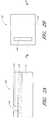
- FIGS. 1A and 1Bare schematic cross-sectional side and top plan views of a partially formed structure, in accordance with some embodiments of the invention.
- FIGS. 2A and 2Bare schematic cross-sectional side and top plan views of the partially formed structure of FIGS. 1A and 1B after forming an opening in a sacrificial layer, in accordance with some embodiments of the invention.
- FIGS. 3A and 3Bare schematic cross-sectional side and top plan views of the partially formed structure of FIGS. 2A and 2B after depositing a seed wall, in accordance with some embodiments of the invention.
- FIGS. 4A and 4Bare schematic cross-sectional side and top plan views of the partially formed structure of FIGS. 3A and 3B after defining openings for deposition inhibiting sidewalls, in accordance with some embodiments of the invention.
- FIGS. 5A , 5 B and 5 Care schematic cross-sectional side and top plan views of the partially formed structure of FIGS. 4A and 4B after forming deposition inhibiting sidewalls and a deposition inhibiting cap layer, in accordance with some embodiments of the invention.
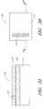
- FIGS. 6A and 6Bare schematic cross-sectional side and top plan views of the partially formed structure of FIGS. 5A and 5B after defining an opening exposing sacrificial material, in accordance with some embodiments of the invention.
- FIG. 7is a schematic, cross-sectional side view of the partially formed structure of FIGS. 6A and 6B after removing sacrificial material to form a mold having an open volume, in accordance with some embodiments of the invention.
- FIG. 8is a schematic perspective view of the partially formed structure of FIG. 7 , in accordance with some embodiments of the invention.
- FIGS. 9A and 9Bare schematic cross-sectional side and top plan views of the partially formed structure of FIGS. 7 and 8 after selectively depositing alternating rows of material in the mold, in accordance with some embodiments of the invention.
- FIGS. 10A , 10 B and 10 Care schematic cross-sectional side and top plan views of the partially formed structure of FIGS. 9A and 9B after selectively removing depositing inhibiting sidewalls, the depositing inhibiting cap layer and one of the alternating rows of material, in accordance with some embodiments of the invention.
- FIG. 11is a schematic perspective view of the partially formed structure of FIGS. 9A and 9B after forming another mold overlying the selectively deposited alternating rows and depositing a second set of alternating rows of material in the other mold, in accordance with some embodiments of the invention.
- FIG. 12is a schematic, cross-sectional side view of the partially formed structure of FIG. 11 after removing the sidewalls and cap layer of the other mold, in accordance with some embodiments of the invention.
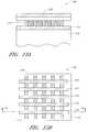
- FIGS. 13A and 13Bare schematic cross-sectional side and top plan views of the partially formed structure of FIG. 12 after selectively removing exposed parts of one of the rows in each of the sets of alternating rows, in accordance with some embodiments of the invention.
- Embodiments of the inventionallow for the formation of exceptionally small features by selectively depositing material.
- a vertically extending surfacee.g., a sidewall, provides a template and a seed surface for the selective deposition of a first material.
- a second materialis then selectively deposited on the first material.
- One of the deposited materialsis selectively removed.
- a plurality of materialscan be removed.
- the remaining rows of materialscan form structures in a final product, thereby avoiding the costs and lower throughput associated with the multiple pattern formation and pattern transfer steps common to some integrated circuit fabrication processes.
- the free-standing rowscan be used as hard masks for patterning an underlying substrate. In these applications, embodiments of the invention can avoid expensive and complicated lithography-based processes typically used to pattern small features.
- deposition processestypically deposit material on all exposed surfaces.
- other exposed surfacesare formed of, or coated by, deposition inhibiting material.
- the seed surfaceis formed of a conductive material that facilitates electrochemical deposition on that surface, while other surfaces are formed of an insulating material that inhibits electrochemical deposition on those surfaces.
- the seed surfaceis formed of a material that allows chemical vapor deposition on that surface, while the other exposed surfaces include deposition inhibiting materials.
- the seed surfaceis provided in a mold having an opening.
- the ceiling, floor and sidewalls that define the interior volume of the moldhaving exposed deposition inhibiting surfaces.
- the seed surfaceforms an interior sidewall of the mold and the opening allows deposition precursors to enter the mold and deposit on the seed sidewall.
- the deposited materialgrows laterally, so that alternating rows of material also grow laterally within the mold.
- the height of the mold openingdetermines the height of the rows and the length of the rows is determined by the distance between opposing deposition inhibiting sidewalls at opposite ends of the rows.
- the moldcan be selectively removed.
- desired rows of the deposited materialcan be removed to form free-standing, laterally-spaced rows formed of the remaining deposited material.
- the deposition processcontrols the widths of the rows.
- the deposition processcan form rows that are thinner than rows that can be directly patterned by typical lithographic processes, such as 193 nm or 248 nm wavelength systems.
- typical lithographic processessuch as 193 nm or 248 nm wavelength systems.
- sublithographic featurescan be formed. For example, features having a critical dimension in the range of about 1 nm to about 100 nm, or about 2 nm to about 50 nm, or about 3 nm to about 30 can be formed
- a mold having a seed wallis formed.
- FIGS. 1A and 1Bcross-sectional side and top plan views of a partially formed structure 100 are illustrated. It will be appreciated that the partially formed structure 100 is a partially formed integrated circuit in some embodiments.
- a substrate 110is overlaid by a bottom deposition inhibiting layer 120 , which is overlaid by a layer 130 of sacrificial material.
- the layers 120 , 130can be deposited by various deposition processes known in the art, the processes selected depending on the identity of the material to be deposited. Examples of deposition processes include vapor deposition processes, such as chemical vapor deposition (CVD), and spin on deposition processes.
- the substrate 110can be various objects over which a pattern will be formed.
- the substrate 110can include a single material, a plurality of layers of different materials, a layer or layers having regions of different materials or different structures in them, etc. In some embodiments, these materials can include semiconductors, insulators, conductors, or combinations thereof.
- the substratecan comprise doped polysilicon, a single crystal electrical device active area, a silicide, or a metal layer, such as a tungsten, aluminum or copper layer, or combinations thereof.
- the substrate 110includes a silicon wafer.
- the bottom deposition inhibiting layer 120can be deposited over the substrate 110 as a separate material, or can be formed by reaction of the substrate 110 to form a deposition inhibiting surface.
- the bottom deposition inhibiting layer 120is chosen based upon the material to be deposited on the seed surface, the deposition process used to deposit the material and processing compatibility with other materials utilized with the partially formed structure 100 .
- the sacrificial material forming the sacrificial layer 130is selectively removable relative to other exposed materials in the partially fabricated structure 100 .
- An etchis “selective” to a material if the etch removes that material without removing a substantial amount of other material(s) exposed to the same etch.
- An example of a sacrificial materialis, without limitation, molybdenum.
- the sacrificial layer 130is etched to form a seed trench 140 .
- the seed trench 140is sized and shaped to accommodate a later-formed seed material, as discussed herein.
- the seed trench 140can be formed by subjecting the sacrificial layer 130 to various pattern forming processes.
- a selectively definable layer(not shown) is provided over the layer 130 .
- the selectively definable layercan be a photoresist layer.
- the photoresist layeris exposed to radiation through a reticle and then developed to leave a pattern including openings corresponding to the seed trench 140 .
- the pattern in the photoresist layeris then transferred to the sacrificial layer 130 to form the seed trench 140 .
- a seed materialis formed in the seed trench 140 .
- the seed materialcan be deposited into the trench, e.g., by chemical vapor deposition, to form a seed wall 150 .
- sidewall trenches 160 a, 160 bare formed by various pattern forming processes known in the art.
- a selectively definable layer(not shown), e.g., a photoresist layer, is provided over the layer 130 .
- the photoresist layeris then exposed to radiation through a reticle and then developed to leave a pattern with openings corresponding to the sidewall trenches 160 a, 160 b.
- the patternis transferred to the sacrificial layer 130 to form the sidewall trenches 160 a, 160 b.
- the sidewall trenches 160 a, 160 bare subsequently filled with deposition inhibiting material to form deposition inhibiting sidewalls.
- the sidewall trenches 160 a, 160 bcontact at least a portion of the seed wall 150 and partially partition off a mass or volume of sacrificial material 132 in the layer 130 .
- a deposition-inhibiting cap layer 170is formed over the sacrificial layer 130 and the seed wall 150 .
- the deposition inhibiting cap layer 170is deposited directly on the sacrificial layer 130 and the seed wall 150 .
- the deposited deposition inhibiting materialfills the trenches 160 a, 160 b ( FIG. 4B ) to form deposition inhibiting sidewalls 170 a, 170 b.
- FIG. 5Bshows, in dotted lines, the locations of the sidewalls 170 a, 170 b underneath the layer 170 a.
- the deposition inhibiting cap layer 170is etched to define an opening 180 that exposes the sacrificial material 132 .
- the location of the opening 180is chosen to facilitate later removal of the sacrificial layer 130 and also to facilitate later selective deposition of materials beneath the layer 170 .
- the opening 180can be formed by various patterning forming and etching methods known in the art. For example, in some embodiments, a photoresist layer (not shown) is deposited over the deposition inhibiting cap layer 170 . The photoresist layer is then patterned to form openings corresponding to the sidewall openings 180 . The pattern is then transferred to the deposition inhibiting cap layer 170 to form the openings 180 . The transfer can be accomplished using an anisotropic etch.
- the sacrificial layer 130is removed, leaving a cavity 180 a.
- the cavity 180 ais delimited by the deposition inhibiting layers 120 , 170 (forming a floor and ceiling, respectively, of the cavity 180 a ) and the deposition inhibiting sidewalls 170 a, 170 b, which together form a mold 172 , with the cavity 180 a being an interior volume of the mold 172 .
- the seed sidewall 150is disposed at one end of the cavity 180 a.
- a plurality of alternating mask materialsare formed.
- two materialsare deposited.
- a first masking materialis deposited on the seed wall 150 .
- the first masking materialis chosen to preferentially deposit on the seed wall 150 relative to the deposition inhibiting layers 120 , 170 and also relative to the deposition inhibiting sidewalls 170 a, 170 b.
- the deposited first masking materialforms a first row 200 .
- the depositioncontinues until the row 200 reaches a desired width 202 .
- the width 202is approximately equal to the desired critical dimension of a feature formed using the row 200 , or to an open volume having a desired width, in embodiments where the row 200 is removed.
- the first row 200roughly tracks the contours of the seed wall 150 . While the seed wall 150 is illustrated extending lengthwise in a straight line for ease of illustration and description, in other embodiments, the seed wall 150 can curve or some portions of the wall 150 can extend at an angle relative to other portions. In some embodiments, the path of the wall 150 corresponds to the shape of the desired path of interconnects in an integrated circuit.
- a second materialis deposited on an exposed side of the first row 200 .
- the second materialis chosen to preferentially deposit on the second row relative to the deposition inhibiting layers 120 , 170 and also relative to the deposition inhibiting sidewalls 170 a, 170 b.
- the deposition of the second materialcontinues to form a second row 210 having a desired width 212 .
- the width 212is equal to the desired critical dimension of a feature formed using the second rows 210 or, where the second rows 210 are to be removed, the width 212 is equal to a desired spacing between the first rows 200 .
- the deposition of the first and second materialscontinues in alternating fashion to form a plurality of alternating first rows 200 of the first material and second rows 210 of the second material.
- the alternating depositionsare continued until a desired number of rows 200 , 210 are formed.
- the depositioncan be accomplished by, e.g., electrochemical deposition, chemical vapor deposition, or atomic layer deposition, depending on the materials forming the seed wall 150 and the first and second masking materials of the rows 200 , 210 , respectively.
- the lateral distance between the opening 180 and the seed wall 150( FIGS. 6A and 6B ) is sufficiently large to extend over all desired rows 200 , 210 .
- the first and second materials for the first and second rows 200 , 210are chosen to be selectively removable relative to each other.
- the materials forming the deposition inhibiting cap layer 170 and the sidewalls 170 a, 170 bare also chosen to be selectively removable relative to the row of the rows 200 , 210 that is to be retained. In the illustrated embodiment, the row 200 is to be retained and other exposed materials are selectively removable relative to that row 200 .
- the deposition inhibiting cap layer 170 and the sidewalls 170 a, 170 bare selectively removed.
- the removalcan be accomplished using a wet or dry etch.
- the second rows 210are removed. Separated, free-standing layers 200 are left remaining over the bottom deposition inhibiting layer 170 .
- the rows 200can be used as mask features to allow a pattern transfer to an underlying material.
- the rows 200can be used to define a pattern in the bottom deposition inhibiting layer 120 .
- the pattern transfercan be accomplished using an anisotropic etch selective for the bottom deposition inhibiting layer 120 .
- the patterncan be further transferred to the substrate 100 .
- the pattern transfercan define various features in the partially formed structure 100 , including, without limitation, interconnects for connecting electrical devices, preferably devices arranged in an array, such as the electrical devices which form a logic array or memory cells in the array region of a memory circuit.
- substrate 100includes a metal and the rows 200 directly define interconnects in the metal.
- the substrate 100includes an insulator and the rows 200 define trenches that are later filled with metal to form interconnects.
- the rows 200can be used as mandrels in a pitch multiplication process.
- Pitch multiplicationis disclosed in U.S. Pat. No. 5,328,810 to Lowrey et al. and U.S. Pat. No. 7,253,118 to Tran et al.
- a blanket layer of spacer materialcan be deposited on the rows 200 .
- the blanket layeris anisotropically etched to define spacers on sidewalls of the rows 200 .
- the rows 200are selectively removed, thereby forming free-standing spacers.
- the free-standing spacersare used as masking features to define patterns in underlying materials.
- the spacerscan be used as mask features to etch an underlying substrate
- the rows 200can form a part of a final structure.
- the rows 200can be used as interconnects.
- the rows 200are formed of an insulator, metal can be deposited in the spaces between the rows 200 to form conductive interconnects.
- multiple levels of selectively deposited rowscan be formed.
- An underlying level of rows including the rows 200 , 210is formed as discussed above with reference to FIGS. 1A-9A .
- the deposition inhibiting cap layer 170is retained and a new mold is formed overlying the layer 170 , in a similar manner as discussed above with reference to FIGS. 1A-8 .
- FIG. 11shows a cross-sectional perspective view in which one of the depositing inhibiting sidewalls on each level is not shown, to allow illustrate of the orientation of rows on each level.
- the new moldincludes a seed sidewall 131 , a deposition-inhibiting sidewall 173 , a depositing-inhibiting cap layer 175 and the deposition inhibiting layer 170 .
- the materials forming the seed sidewall 131 , the deposition-inhibiting sidewall 173 , and the depositing-inhibiting cap layer 175can be the same as that forming the seed sidewall 130 , the deposition-inhibiting sidewall 170 a and the deposition inhibiting layer 170 , respectively.
- the new moldis formed at a desired orientation relative to the underlying rows 200 , 210 . In some embodiments, the new mold is oriented to form alternating rows of different masking materials which crisscross the rows 200 , 210 .
- rows 204 formed of the first materialare formed alternating with rows 214 formed of the second material.
- the rows 204 and 214are exposed.
- the rows 204 and 214are exposed by removing the sidewalls (including the illustrated sidewall 173 of FIG. 11 ) and the cap layer 175 .
- a crisscrossing pattern of rows 200 and 204is formed.
- the rows 200 , 204define open columns in the spaces between them.
- the crisscrossing patterncan be utilized as part of a final structure (e.g., crossing interconnects), or as a mask to form a pattern in underlying materials.
- the openings in the crisscrossing patterncan be filled to form isolated pillar shapes, including pillars having rectangular or cubic horizontal cross-sectional areas. Such an arrangement can be useful for forming, e.g., contact plugs.
- the pillarscan advantageously be applied in some arrangements for patterning arrays of features, particularly dense arrays of features, such as capacitors for memory applications, including DRAM, or as memory elements for MRAM or STTRAM.
- the various materials for the deposition inhibiting layers 120 , 170 , the deposition inhibiting sidewalls 170 a, 170 b, and the seed sidewall 150are chosen based upon the materials that will be deposited in the cavity 180 a ( FIG. 7 ), and based upon, e.g., etch and deposition compatibility with the other materials forming the partially formed structure 100 .
- the bottom deposition inhibiting layer 120is formed of an insulator and the seed wall 150 is formed of a conductor.
- the first and second materialsare deposited by electrochemical deposition.
- gold and silverare used as the first and second materials.
- gold and nickelare used.
- Plating solutions including the desired metal speciescan be introduced into the opening 180 .
- the plating solutioncontains both materials.
- the seed wall 150can be connected to a power source and deposition occurs when current is flowed through the solution.
- the seed wall 150can be connected to a power source through the substrate 110 .
- the seed wall 150can be made to extend through the deposition inhibiting layer 120 to contact the substrate 110 , which may be formed of conductive or semiconductive material and which is connected to one of the electrodes of the power source.
- the width of each rowcan be controlled by selection of the charge passed during the deposition and by selection of the concentrations of the metal species. For example, to increase the width of a row formed by one of the metals, the concentration of that metal can be increased. Suitable selective deposition methods are discussed in Qin et al., Science, Vol. 309, Jul. 1, 2005, pp. 113-115.
- one of the metalscan be removed by an appropriate etch.
- Nican be selectively removed relative to gold using a wet etch, such as a wet etch including concentrated HNO 3 .
- silver rowscan be selectively removed using a wet etch formed of methanol, 30% ammonium hydroxide and 30% hydrogen peroxide (4:1:1 v/v/v). Suitable etch methods are discussed in Qin et al., Science, Vol. 309, Jul. 1, 2005, pp. 113-115.
- materialsare selectively deposited in the cavity 180 a by atomic layer deposition (ALD).
- ALDatomic layer deposition
- the seed sidewall 150is formed of silicon
- the deposition inhibiting layers 120 , 170 , and the deposition inhibiting sidewalls 170 a, 170 bare formed of silicon oxide having a chemically modified surface.
- the deposition inhibiting layers 120 , 170 , and the deposition inhibiting sidewalls 170 a, 170 bare formed as described above, and then exposed to another chemical species to form a deposition inhibiting layer on exposed silicon oxide surfaces.
- ODTSoctadecyltrichlorosilane
- SAMself-assmbled monolayer
- the row 200is formed by selective atomic layer deposition on the seed sidewall 150 .
- the row 200can be formed of HfO 2 deposited using tetrakis(dimethylamido)hafnium(IV) (Hf[N(CH 3 ) 2 ] 4 and water. Suitable methods for forming deposition inhibiting surfaces and depositing HfO 2 are discussed in Chen, Applied Physics Letters 86, 191910 (2005).
- the row 210is subsequently selectively deposited by atomic layer deposition on the deposited row 200 .
- rutheniumdeposited on the sidewall of the HfO 2 row 200 to form the row 210 .
- Suitable methods for selectively depositing Ruare discussed in Park, Applied Physics Letters 86, 051903 (2005).
- the deposition of the HfO 2 and the Ruare alternately repeated to form a desired number of rows 200 , 210 . Subsequently, the rows 200 , 210 are exposed, as discussed herein, and one of the rows is removed by exposure to etchant, e.g., in a wet etch selective for the material of one of the rows 200 , 210 relative to other exposed materials.
- etchante.g., in a wet etch selective for the material of one of the rows 200 , 210 relative to other exposed materials.
- the inside surfaces of the cavity 180 aare exposed to ODTS one or more times during the deposition of the rows 200 , 210 to build up the ODTS layer on those inside surfaces.
- atomic layer depositionallows the rows 200 , 210 to be formed with high precision regarding the widths 202 , 212 , since the widths can be controlled by the number of deposition cycles performed, as known in the art. As a result, exceptionally uniform rows 200 , 210 can be formed.
- the layer by layer deposition mechanism of ALDallows the formation, as desired, of rows 200 , 210 having different widths.
- the selectively deposited rows disclosed hereincan be used in various other applications where the formation of patterns with very small features is desired.
- the preferred embodimentscan be applied to form gratings, disk drives, storage media or templates or masks for other lithography techniques, including X-ray or imprint lithography.
- multiple levels of the rowscan be utilized in various light bending applications, in which spatially isolated blocks of material are formed “floating” and separated from other blocks of materials.
- Floating blocks of materialcan be formed by depositing material into vias formed by crisscrossing rows of masking material ( FIG. 13B ) and the vias can be overlaid with material and additional vias can be formed and filled at a higher level.
- the blocks of materialcan be the first or second masking materials themselves, with the molds dimensioned to form short blocks, rather than long rows of masking material.
- the deposition inhibiting materialcan be used to separate neighboring pluralities of the blocks.
- a plurality of the molds 172can be formed across the surface of the substrate 110 in a desired pattern.
- the molds 172can be formed in a regular array over the substrate 110 to pattern a regular array of features.
- these featurescan be advantageously applied to form features in integrated circuit utilizing arrays of features, e.g., to form logic circuitry or memory devices, including flash memory or DRAM.
- processing through the maskcan involve subjecting material(s) underlying the mask materials to any semiconductor fabrication process.
- processingcan involve ion implantation, diffusion doping, depositing, oxidizing (particularly with use of a hard mask under the polymer mask), nitridizing, etc. through the mask layers and onto underlying layers.
- the maskcan be used as a stop or barrier for chemical mechanical polishing (CMP) or CMP can be performed on various material(s) to allow for both planarization and etching.
- CMPchemical mechanical polishing
- a patterning methodcomprises providing a substrate having a top surface that comprises a deposition inhibiting material.
- a mass of a sacrificial materialis provided over the deposition inhibiting material.
- a seed wallis formed on one side of the mass of the sacrificial material.
- First and second deposition inhibiting wallsare formed on opposite sides of the mass of the sacrificial material.
- the seed wallis disposed between and contacting the first and second deposition inhibiting walls.
- a deposition inhibiting cap layeris formed over the mass of the sacrificial material.
- the mass of the sacrificial materialis selectively removed to form an open volume at least partially bounded by the seed wall, the first and second deposition inhibiting walls, the deposition inhibiting material and the cap layer.
- First and second materialsare alternatingly deposited in the open volume.
- a method for forming a patterncomprises providing a substrate.
- a hollow moldis provided overlying the substrate.
- the moldhas an opening into an open internal volume and a seed sidewall partially delimiting the open volume.
- a first materialis selectively deposited on the seed sidewall in the open volume.
- a second materialis selectively deposited on a side of the first material in the open volume.
- a method for depositing materials in a desired patterncomprises providing a substrate.
- the substrateis alternatingly exposed to first and second material precursors to deposit first and second materials on a first level.
- Depositing the first and second materialssequentially laterally grows a first plurality of alternating rows of the first and the second materials.
- One of the first and second materialsis selectively removed relative to the other of the first and second materials.
Landscapes
- Engineering & Computer Science (AREA)
- Physics & Mathematics (AREA)
- Condensed Matter Physics & Semiconductors (AREA)
- General Physics & Mathematics (AREA)
- Manufacturing & Machinery (AREA)
- Computer Hardware Design (AREA)
- Microelectronics & Electronic Packaging (AREA)
- Power Engineering (AREA)
- Chemical & Material Sciences (AREA)
- Inorganic Chemistry (AREA)
- Internal Circuitry In Semiconductor Integrated Circuit Devices (AREA)
- Semiconductor Memories (AREA)
Abstract
Description
Claims (16)
Priority Applications (8)
| Application Number | Priority Date | Filing Date | Title |
|---|---|---|---|
| US12/140,928US8404600B2 (en) | 2008-06-17 | 2008-06-17 | Method for forming fine pitch structures |
| PCT/US2009/045515WO2009155067A2 (en) | 2008-06-17 | 2009-05-28 | Method for forming fine pitch structures |
| CN200980122694.3ACN102067282B (en) | 2008-06-17 | 2009-05-28 | Method for forming fine pitch structures |
| EP09767378AEP2304771A2 (en) | 2008-06-17 | 2009-05-28 | Method for forming fine pitch structures |
| KR1020117001126AKR20110030599A (en) | 2008-06-17 | 2009-05-28 | How to Form Fine Pitch Structures |
| TW098119261ATWI518740B (en) | 2008-06-17 | 2009-06-09 | Method of forming a fine pitch structure |
| US13/794,084US8846537B2 (en) | 2008-06-17 | 2013-03-11 | Method for forming fine pitch structures |
| US14/497,773US20150011085A1 (en) | 2008-06-17 | 2014-09-26 | Method for forming fine pitch structures |
Applications Claiming Priority (1)
| Application Number | Priority Date | Filing Date | Title |
|---|---|---|---|
| US12/140,928US8404600B2 (en) | 2008-06-17 | 2008-06-17 | Method for forming fine pitch structures |
Related Child Applications (1)
| Application Number | Title | Priority Date | Filing Date |
|---|---|---|---|
| US13/794,084DivisionUS8846537B2 (en) | 2008-06-17 | 2013-03-11 | Method for forming fine pitch structures |
Publications (2)
| Publication Number | Publication Date |
|---|---|
| US20090311867A1 US20090311867A1 (en) | 2009-12-17 |
| US8404600B2true US8404600B2 (en) | 2013-03-26 |
Family
ID=41415184
Family Applications (3)
| Application Number | Title | Priority Date | Filing Date |
|---|---|---|---|
| US12/140,928Active2032-01-25US8404600B2 (en) | 2008-06-17 | 2008-06-17 | Method for forming fine pitch structures |
| US13/794,084ActiveUS8846537B2 (en) | 2008-06-17 | 2013-03-11 | Method for forming fine pitch structures |
| US14/497,773AbandonedUS20150011085A1 (en) | 2008-06-17 | 2014-09-26 | Method for forming fine pitch structures |
Family Applications After (2)
| Application Number | Title | Priority Date | Filing Date |
|---|---|---|---|
| US13/794,084ActiveUS8846537B2 (en) | 2008-06-17 | 2013-03-11 | Method for forming fine pitch structures |
| US14/497,773AbandonedUS20150011085A1 (en) | 2008-06-17 | 2014-09-26 | Method for forming fine pitch structures |
Country Status (6)
| Country | Link |
|---|---|
| US (3) | US8404600B2 (en) |
| EP (1) | EP2304771A2 (en) |
| KR (1) | KR20110030599A (en) |
| CN (1) | CN102067282B (en) |
| TW (1) | TWI518740B (en) |
| WO (1) | WO2009155067A2 (en) |
Cited By (1)
| Publication number | Priority date | Publication date | Assignee | Title |
|---|---|---|---|---|
| US20100227018A1 (en)* | 2009-03-03 | 2010-09-09 | Commissariat A L' Energie Atomique | Method to fabricate a mould for lithography by nano-imprinting |
Families Citing this family (14)
| Publication number | Priority date | Publication date | Assignee | Title |
|---|---|---|---|---|
| KR20130002527A (en)* | 2011-06-29 | 2013-01-08 | 엘지이노텍 주식회사 | Method of manufacturing a nanowire |
| US20140065838A1 (en)* | 2012-08-31 | 2014-03-06 | Carolyn R. Ellinger | Thin film dielectric layer formation |
| US8927434B2 (en)* | 2012-08-31 | 2015-01-06 | Eastman Kodak Company | Patterned thin film dielectric stack formation |
| US8791023B2 (en)* | 2012-08-31 | 2014-07-29 | Eastman Kodak Company | Patterned thin film dielectric layer formation |
| US9793159B2 (en) | 2013-09-27 | 2017-10-17 | Intel Corporation | Previous layer self-aligned via and plug patterning for back end of line (BEOL) interconnects |
| EP3050087B1 (en)* | 2013-09-27 | 2020-04-29 | Intel Corporation | Subtractive self-aligned via and plug patterning for back end of line (beol) interconnects |
| CN105518837B (en) | 2013-09-27 | 2019-04-16 | 英特尔公司 | Self-aligned via and plug patterning for back-end-of-line (BEOL) interconnects |
| KR102171263B1 (en)* | 2014-08-21 | 2020-10-28 | 삼성전자 주식회사 | Integrated circuit device having single crystal silicon thin film and method of manufacturing the same |
| US10043672B2 (en)* | 2016-03-29 | 2018-08-07 | Lam Research Corporation | Selective self-aligned patterning of silicon germanium, germanium and type III/V materials using a sulfur-containing mask |
| US9607886B1 (en)* | 2016-06-30 | 2017-03-28 | International Business Machines Corporation | Self aligned conductive lines with relaxed overlay |
| US9941118B2 (en)* | 2016-08-22 | 2018-04-10 | International Business Machines Corporation | Dense vertical nanosheet |
| TWI721231B (en)* | 2016-11-16 | 2021-03-11 | 日商東京威力科創股份有限公司 | Methods of sub-resolution substrate patterning |
| US10515896B2 (en)* | 2017-08-31 | 2019-12-24 | Taiwan Semiconductor Manufacturing Co., Ltd. | Interconnect structure for semiconductor device and methods of fabrication thereof |
| CN113991017B (en)* | 2021-09-18 | 2025-02-11 | 长鑫存储技术有限公司 | A capacitor array structure, a manufacturing method thereof and a semiconductor memory device |
Citations (23)
| Publication number | Priority date | Publication date | Assignee | Title |
|---|---|---|---|---|
| JPH02143527A (en) | 1988-11-25 | 1990-06-01 | Sony Corp | Wiring formation |
| JPH033375A (en) | 1989-05-31 | 1991-01-09 | Fujitsu Ltd | Manufacture of oxide superconducting device |
| US5328810A (en) | 1990-05-07 | 1994-07-12 | Micron Technology, Inc. | Method for reducing, by a factor or 2-N, the minimum masking pitch of a photolithographic process |
| US5772905A (en) | 1995-11-15 | 1998-06-30 | Regents Of The University Of Minnesota | Nanoimprint lithography |
| US6319853B1 (en) | 1998-01-09 | 2001-11-20 | Mitsubishi Denki Kabushiki Kaisha | Method of manufacturing a semiconductor device using a minute resist pattern, and a semiconductor device manufactured thereby |
| JP2003155365A (en) | 2001-11-22 | 2003-05-27 | Toshiba Corp | Processing method and molded body |
| US20030170995A1 (en) | 1995-11-15 | 2003-09-11 | Chou Stephen Y. | Method and apparatus for high density nanostructures |
| US6667237B1 (en) | 2000-10-12 | 2003-12-23 | Vram Technologies, Llc | Method and apparatus for patterning fine dimensions |
| US20050112886A1 (en) | 2001-12-28 | 2005-05-26 | Kabushiki Kaisha Toshiba | Light-emitting device and method for manufacturing the same |
| US6911400B2 (en) | 2002-11-05 | 2005-06-28 | International Business Machines Corporation | Nonlithographic method to produce self-aligned mask, articles produced by same and compositions for same |
| US6926953B2 (en) | 2001-10-05 | 2005-08-09 | Wisconsin Alumni Research Foundation | Guided self-assembly of block copolymer films on interferometrically nanopatterned substrates |
| US20050280118A1 (en) | 2004-06-18 | 2005-12-22 | Taiwan Semiconductor Manufacturing Company, Ltd. | Methods of manufacturing metal-silicide features |
| US20060216923A1 (en) | 2005-03-28 | 2006-09-28 | Tran Luan C | Integrated circuit fabrication |
| WO2006101695A1 (en) | 2005-03-15 | 2006-09-28 | Micron Technology, Inc. | Pitch reduced patterns relative to photolithography features |
| US7115525B2 (en) | 2004-09-02 | 2006-10-03 | Micron Technology, Inc. | Method for integrated circuit fabrication using pitch multiplication |
| US7141866B1 (en)* | 2004-04-16 | 2006-11-28 | Hewlett-Packard Development Company, L.P. | Apparatus for imprinting lithography and fabrication thereof |
| US20060281266A1 (en) | 2005-06-09 | 2006-12-14 | Wells David H | Method and apparatus for adjusting feature size and position |
| WO2007027686A2 (en) | 2005-09-01 | 2007-03-08 | Micron Technology, Inc. | Mask patterns with spacers for pitch multiplication and methods of forming the same |
| US7208379B2 (en) | 2004-11-29 | 2007-04-24 | Texas Instruments Incorporated | Pitch multiplication process |
| US20070249170A1 (en) | 2006-04-25 | 2007-10-25 | David Kewley | Process for improving critical dimension uniformity of integrated circuit arrays |
| US20070281219A1 (en) | 2006-06-01 | 2007-12-06 | Sandhu Gurtej S | Masking techniques and contact imprint reticles for dense semiconductor fabrication |
| US20080057687A1 (en) | 2006-09-01 | 2008-03-06 | Ngimat Co., A Georgia Corporation | Selective area deposition and devices formed therefrom |
| US20120138571A1 (en)* | 2008-02-05 | 2012-06-07 | International Business Machines Corporation | Pattern formation employing self-assembled material |
Family Cites Families (11)
| Publication number | Priority date | Publication date | Assignee | Title |
|---|---|---|---|---|
| IL131037A (en)* | 1999-07-22 | 2004-06-20 | Israel Atomic Energy Comm | Method for making threedimensional photonic band-gap crystals |
| US7252861B2 (en)* | 2002-05-07 | 2007-08-07 | Microfabrica Inc. | Methods of and apparatus for electrochemically fabricating structures via interlaced layers or via selective etching and filling of voids |
| US20080105646A1 (en)* | 2002-05-07 | 2008-05-08 | Microfabrica Inc. | Multi-step Release Method for Electrochemically Fabricated Structures |
| US7195989B2 (en)* | 2003-05-07 | 2007-03-27 | Microfabrica Inc. | Electrochemical fabrication methods using transfer plating of masks |
| US6638879B2 (en)* | 2001-12-06 | 2003-10-28 | Macronix International Co., Ltd. | Method for forming nitride spacer by using atomic layer deposition |
| US20080283405A1 (en)* | 2003-05-01 | 2008-11-20 | Johns Hopkins University | Method for Producing Patterned Structures by Printing a Surfactant Resist on a Substrate for Electrodeposition |
| US7258895B2 (en)* | 2003-08-06 | 2007-08-21 | Micron Technology, Inc. | Methods of forming material on a substrate, and a method of forming a field effect transistor gate oxide on a substrate |
| US7018917B2 (en)* | 2003-11-20 | 2006-03-28 | Asm International N.V. | Multilayer metallization |
| KR100674970B1 (en)* | 2005-04-21 | 2007-01-26 | 삼성전자주식회사 | Fine pitch pattern formation method using double spacers |
| US8084087B2 (en)* | 2007-02-14 | 2011-12-27 | The Board Of Trustees Of The Leland Stanford Junior University | Fabrication method of size-controlled, spatially distributed nanostructures by atomic layer deposition |
| US8262916B1 (en)* | 2009-06-30 | 2012-09-11 | Microfabrica Inc. | Enhanced methods for at least partial in situ release of sacrificial material from cavities or channels and/or sealing of etching holes during fabrication of multi-layer microscale or millimeter-scale complex three-dimensional structures |
- 2008
- 2008-06-17USUS12/140,928patent/US8404600B2/enactiveActive
- 2009
- 2009-05-28KRKR1020117001126Apatent/KR20110030599A/ennot_activeAbandoned
- 2009-05-28EPEP09767378Apatent/EP2304771A2/ennot_activeWithdrawn
- 2009-05-28WOPCT/US2009/045515patent/WO2009155067A2/enactiveApplication Filing
- 2009-05-28CNCN200980122694.3Apatent/CN102067282B/enactiveActive
- 2009-06-09TWTW098119261Apatent/TWI518740B/enactive
- 2013
- 2013-03-11USUS13/794,084patent/US8846537B2/enactiveActive
- 2014
- 2014-09-26USUS14/497,773patent/US20150011085A1/ennot_activeAbandoned
Patent Citations (25)
| Publication number | Priority date | Publication date | Assignee | Title |
|---|---|---|---|---|
| JPH02143527A (en) | 1988-11-25 | 1990-06-01 | Sony Corp | Wiring formation |
| JPH033375A (en) | 1989-05-31 | 1991-01-09 | Fujitsu Ltd | Manufacture of oxide superconducting device |
| US5328810A (en) | 1990-05-07 | 1994-07-12 | Micron Technology, Inc. | Method for reducing, by a factor or 2-N, the minimum masking pitch of a photolithographic process |
| US5772905A (en) | 1995-11-15 | 1998-06-30 | Regents Of The University Of Minnesota | Nanoimprint lithography |
| US20030170995A1 (en) | 1995-11-15 | 2003-09-11 | Chou Stephen Y. | Method and apparatus for high density nanostructures |
| US6319853B1 (en) | 1998-01-09 | 2001-11-20 | Mitsubishi Denki Kabushiki Kaisha | Method of manufacturing a semiconductor device using a minute resist pattern, and a semiconductor device manufactured thereby |
| US6667237B1 (en) | 2000-10-12 | 2003-12-23 | Vram Technologies, Llc | Method and apparatus for patterning fine dimensions |
| US6926953B2 (en) | 2001-10-05 | 2005-08-09 | Wisconsin Alumni Research Foundation | Guided self-assembly of block copolymer films on interferometrically nanopatterned substrates |
| JP2003155365A (en) | 2001-11-22 | 2003-05-27 | Toshiba Corp | Processing method and molded body |
| US20050112886A1 (en) | 2001-12-28 | 2005-05-26 | Kabushiki Kaisha Toshiba | Light-emitting device and method for manufacturing the same |
| US6911400B2 (en) | 2002-11-05 | 2005-06-28 | International Business Machines Corporation | Nonlithographic method to produce self-aligned mask, articles produced by same and compositions for same |
| US7141866B1 (en)* | 2004-04-16 | 2006-11-28 | Hewlett-Packard Development Company, L.P. | Apparatus for imprinting lithography and fabrication thereof |
| TW200601458A (en) | 2004-06-18 | 2006-01-01 | Taiwan Semiconductor Mfg Co Ltd | Microelectronic devices and fabrication methods thereof |
| US20050280118A1 (en) | 2004-06-18 | 2005-12-22 | Taiwan Semiconductor Manufacturing Company, Ltd. | Methods of manufacturing metal-silicide features |
| US7268065B2 (en)* | 2004-06-18 | 2007-09-11 | Taiwan Semiconductor Manufacturing Company, Ltd. | Methods of manufacturing metal-silicide features |
| US7115525B2 (en) | 2004-09-02 | 2006-10-03 | Micron Technology, Inc. | Method for integrated circuit fabrication using pitch multiplication |
| US7208379B2 (en) | 2004-11-29 | 2007-04-24 | Texas Instruments Incorporated | Pitch multiplication process |
| WO2006101695A1 (en) | 2005-03-15 | 2006-09-28 | Micron Technology, Inc. | Pitch reduced patterns relative to photolithography features |
| US20060216923A1 (en) | 2005-03-28 | 2006-09-28 | Tran Luan C | Integrated circuit fabrication |
| US20060281266A1 (en) | 2005-06-09 | 2006-12-14 | Wells David H | Method and apparatus for adjusting feature size and position |
| WO2007027686A2 (en) | 2005-09-01 | 2007-03-08 | Micron Technology, Inc. | Mask patterns with spacers for pitch multiplication and methods of forming the same |
| US20070249170A1 (en) | 2006-04-25 | 2007-10-25 | David Kewley | Process for improving critical dimension uniformity of integrated circuit arrays |
| US20070281219A1 (en) | 2006-06-01 | 2007-12-06 | Sandhu Gurtej S | Masking techniques and contact imprint reticles for dense semiconductor fabrication |
| US20080057687A1 (en) | 2006-09-01 | 2008-03-06 | Ngimat Co., A Georgia Corporation | Selective area deposition and devices formed therefrom |
| US20120138571A1 (en)* | 2008-02-05 | 2012-06-07 | International Business Machines Corporation | Pattern formation employing self-assembled material |
Non-Patent Citations (41)
| Title |
|---|
| "Molecular Thermodynamics & Statistical Mechanics (MTSM) Research Group"; www.engr.wisc.edu/groups/mtsm/research.shtml; Oct. 28, 2005; 7 pgs. |
| "Polymer Research Laboratory"; www.princeton.edu/~polymer/block.html; Oct. 27, 2005; 2 pgs. |
| "Polymer Research Laboratory"; www.princeton.edu/˜polymer/block.html; Oct. 27, 2005; 2 pgs. |
| Bates et al.; "Block Copolymers-Designer Soft Materials"; Physics Today; Feb. 1999, vol. 52, No. 2; pp. 32-38. |
| Black et al. "IBM demos new nanotechnology method to build chip components. Creates nanocrystal memory devices using self assembly technique compatible with conventional semiconductor processing," http://domino.research.ibm.com/comm/pr.nsf/pages/news.20031208-selfassembly.html; Dec. 8, 2003. |
| Black et al. "Nanometer-Scale Pattern Registration and Aignment by Directed Diblock Copolymer Self-Assembly," IEEE Transactions on Nanotechnology, vol. 3, No. 3 (Sep. 2004); pp. 412-415. |
| Callahan, Tim; "Pattern Formation"; Mathematics Department; www.math.lsa.umich.edu/~timcall/patterns/; Oct. 28, 2005; 5 pgs. |
| Callahan, Tim; "Pattern Formation"; Mathematics Department; www.math.lsa.umich.edu/˜timcall/patterns/; Oct. 28, 2005; 5 pgs. |
| Carcia et al., "Thin films for Phase-shift Masks," Vacuum and Thin Film, IHS Publishing Group, 14-21 (Sep. 1999). |
| Cerofolini et al., "Strategies for nanoelectronics", Microelectronic Engineering, 81 (2005), pg. 405-419.* |
| Chen et al., Achieving area-selective atomic layer deposition on patterned substrates by selective surface modification, Applied Physics Letters 86, 191910-1-191910-3 (2005). |
| Cheng et al. "Fabrication of nanostructures with long-range order using block copolymer lithography," Applied Physics Letters, vol. 81, No. 19, pp. 3657-3659 (Nov. 4, 2002). |
| Chou et al., Nanoimprint lithography, J.Vac. Sci. Technol. B 14(6), Nov./Dec. 1996, American Vacuum Society. |
| Cochran, Eric W.; Chemical Engineering-Iowa State University; www.iastate.edu/~ch-e/faculty/cochran.htm; Oct. 28, 2005; 2 pgs. |
| Cochran, Eric W.; Chemical Engineering—Iowa State University; www.iastate.edu/˜ch—e/faculty/cochran.htm; Oct. 28, 2005; 2 pgs. |
| Edwards et al., "Precise Control over Molecular Dimensions of Block-Copolymer Domains Using the Interfacial Energy of Chemically Nanopatterned Substrates," Advanced Materials, 16, No. 15, (Aug. 4, 2004); pp. 1315-1319. |
| Fasolka et al.; "Block Copolymer Thin Films: Physics and Applications"; Annu. Rev. Mater. Res. 2001.31:323-355. |
| Guarini et al., "Low voltage, scalable nanocrystal FLASH memory fabricated by templated self-assembly," Electron Devices Meeting 2003, IEDM 03 Technical Digest. IEEE International Dec. 8-10, 2003, pp. 22.2.1-22.2.4. |
| Guarini et al.; "Optimization of Diblock Copolymer Thin Film Self Assembly"; Adv. Mater. 2002, 14, No. 1, Sep. 16; pp. 1290-1294. |
| Herr, Daniel J.C.; "The Extensibility of Optical Patterning Via Directed Self-Assembly of Nano-Engineered Imaging Materials"; Future Fab Intl.; www.future-fab.corn; 8 pgs.; Oct. 27, 2005. |
| http://mrsec.uchicago.edu/Nuggets/Stripes/; Oct. 27, 2005; 3 pgs. |
| International Search Report (International Application No. PCT/US2007/011524). |
| International Search Report dated Jan. 12, 2010 in counterpart PCT Application No. PCT/US2009/045515. |
| Jeong et al.; "Asymmetric Block Copolymers with Homopolymers: Routes to Multiple Length Scale Nanostructures"; Adv. Mater. 2002, 14, No. 4, Feb. 19; pp. 274-276. |
| Jeong et al.; "Volume Contractions Induced by Crosslinking: A Novel Route to Nanoporous Polymer Films"; Adv. Mater. 2003, 15, No. 15, Aug. 5; pp. 1247-1250. |
| Kim et al., "Epitaxial self-assembly of block copolymers on lithographically defined nanopatterned substrates," Nature 424, 411-414 (Jul. 24, 2003). |
| Limary et al.; "Block Copolymer Thin Films Above and Below the Order-Disorder Transition Temperature"; Mat.Res.Soc.Symp. vol. 629; (2000) Materials Research Society; 6 pgs. |
| Nealy et al, "Directed assembly of imaging layers for sub-30 nm lithography", First International Nanotechnology Conference on Communication and Cooperation, Jun. 2005, 2 pages. |
| Ngandu, K., "Resolution Enhancement Techniques for Optical Lithography," NNIN REU Research Accomplishments, 90-91 (2004). |
| Office Action dated Sep. 18, 2012 in corresponding PRC (China) Patent Application No. 200980122694.3. |
| Park et al., "Enabling Nanotechnology with Self-Assembled Block Copolymer Patterns," Polymer, Elsevier Science Publishers, B.V., GB, vol. 44, No. 22 pp. 6725-6760 (Oct. 2003). |
| Park et al., Microcontact patterning of ruthenium gate electrodes by selective area atomic layer deposition, Applied Physics Letters 86, 051903 (2005). |
| Qin et al., On Wire Lithography, www.sciencemag.org, vol. 309, Jul. 1, 2005, p. 113-115. |
| Rockford et al., "Polymers on Nanoperiodic, Heterogeneous Surfaces," Physical Review Letters APS USA, vol. 82, No. 12 (Mar. 22, 1999). |
| Sinha et al., Area-Selective ALD of Titanium Dioxide Using Lithographically Defind Poly (methyl methacrylate) Films, Journal of the Electrochemical Society, 153 (5) G465-G469 (2006). |
| Sony CS-News vol. 29, 2002, Next Generation Low-Cost Electron Beam Lithography Fabrication Technology, wvvw.sony.net/Products/SC-HP/cx-news/vol29/pdf/mask.pdf. |
| Stoykovich et al., "Directed Assembly of Block Copolymer Blends into Nonregular Device-Oriented Structures," Science, vol. 308, 1442-1446 (Jun. 3, 2005). |
| Tirrell et al.; "Self-Assembly in Materials Synthesis"; MRS Bulletin; vol. 30; Oct. 2005; pp. 700-704. |
| U.S. Office Action of Apr. 17, 2008 in U.S. Appl. No. 11/389,581, filed Mar. 23, 2006. |
| Wang et al., "Symmetric diblock copolymer thin films confined between homogenous and patterned surfaces: Simulations and theory," Journal of Chemical Physics vol. 112, No. 22 (2000); pp. 9996-10010. |
| Zheng et al.; "Structural Evolution and Alignment of Cylinder-Forming PS-b-PEP Thin Films in Confinement Studied by Time-Lapse Atomic Force Microscopy"; Mater.Res.Soc.Symp.Proc. vol. 854E (2005) Materials Research Society; 4 pgs. |
Cited By (2)
| Publication number | Priority date | Publication date | Assignee | Title |
|---|---|---|---|---|
| US20100227018A1 (en)* | 2009-03-03 | 2010-09-09 | Commissariat A L' Energie Atomique | Method to fabricate a mould for lithography by nano-imprinting |
| US8778195B2 (en)* | 2009-03-03 | 2014-07-15 | Commissariat A L' Energie Atomique | Method to fabricate a mould for lithography by nano-imprinting |
Also Published As
| Publication number | Publication date |
|---|---|
| US20130252420A1 (en) | 2013-09-26 |
| WO2009155067A2 (en) | 2009-12-23 |
| US8846537B2 (en) | 2014-09-30 |
| CN102067282A (en) | 2011-05-18 |
| US20090311867A1 (en) | 2009-12-17 |
| TW201003739A (en) | 2010-01-16 |
| EP2304771A2 (en) | 2011-04-06 |
| CN102067282B (en) | 2013-08-14 |
| KR20110030599A (en) | 2011-03-23 |
| WO2009155067A3 (en) | 2010-02-25 |
| US20150011085A1 (en) | 2015-01-08 |
| TWI518740B (en) | 2016-01-21 |
Similar Documents
| Publication | Publication Date | Title |
|---|---|---|
| US8404600B2 (en) | Method for forming fine pitch structures | |
| KR101603800B1 (en) | Integrated circuit, electrical device comprising the same and methods for forming the same | |
| US7759197B2 (en) | Method of forming isolated features using pitch multiplication | |
| US9082829B2 (en) | Methods for forming arrays of small, closely spaced features | |
| CN100483768C (en) | Semiconductor unit, memory unit and memory unit array and forming method thereof | |
| US8663532B2 (en) | Masking techniques and contact imprint reticles for dense semiconductor fabrication | |
| KR101449772B1 (en) | Efficient pitch multiplication process | |
| KR20080045729A (en) | Mask patterns with spacers for pitch multiplication and method of forming the same | |
| CN111466023A (en) | Three-dimensional memory device including three-dimensional bit line discharge transistor and method of making the same | |
| CN101772832A (en) | Semiconductor structures including tight pitch contacts and methods to form same | |
| US12255154B2 (en) | Three-dimensional memory device with orthogonal memory opening and support opening arrays and method of making thereof | |
| CN116825838A (en) | Semiconductor structure and manufacturing method thereof, memory and manufacturing method thereof | |
| CN105448926B (en) | Memory element and manufacturing method thereof | |
| US20250176179A1 (en) | Three-dimensional memory device with dummy slit regions and methods of making the same | |
| JP5229588B2 (en) | Simplified pitch doubling process | |
| JP5229588B6 (en) | Simplified pitch doubling process |
Legal Events
| Date | Code | Title | Description |
|---|---|---|---|
| AS | Assignment | Owner name:MICRON TECHNOLOGY, INC., IDAHO Free format text:ASSIGNMENT OF ASSIGNORS INTEREST;ASSIGNOR:SANDHU, GURTEJ;REEL/FRAME:021116/0583 Effective date:20080612 | |
| FEPP | Fee payment procedure | Free format text:PAYOR NUMBER ASSIGNED (ORIGINAL EVENT CODE: ASPN); ENTITY STATUS OF PATENT OWNER: LARGE ENTITY | |
| STCF | Information on status: patent grant | Free format text:PATENTED CASE | |
| AS | Assignment | Owner name:U.S. BANK NATIONAL ASSOCIATION, AS COLLATERAL AGENT, CALIFORNIA Free format text:SECURITY INTEREST;ASSIGNOR:MICRON TECHNOLOGY, INC.;REEL/FRAME:038669/0001 Effective date:20160426 Owner name:U.S. BANK NATIONAL ASSOCIATION, AS COLLATERAL AGEN Free format text:SECURITY INTEREST;ASSIGNOR:MICRON TECHNOLOGY, INC.;REEL/FRAME:038669/0001 Effective date:20160426 | |
| AS | Assignment | Owner name:MORGAN STANLEY SENIOR FUNDING, INC., AS COLLATERAL AGENT, MARYLAND Free format text:PATENT SECURITY AGREEMENT;ASSIGNOR:MICRON TECHNOLOGY, INC.;REEL/FRAME:038954/0001 Effective date:20160426 Owner name:MORGAN STANLEY SENIOR FUNDING, INC., AS COLLATERAL Free format text:PATENT SECURITY AGREEMENT;ASSIGNOR:MICRON TECHNOLOGY, INC.;REEL/FRAME:038954/0001 Effective date:20160426 | |
| FPAY | Fee payment | Year of fee payment:4 | |
| AS | Assignment | Owner name:U.S. BANK NATIONAL ASSOCIATION, AS COLLATERAL AGENT, CALIFORNIA Free format text:CORRECTIVE ASSIGNMENT TO CORRECT THE REPLACE ERRONEOUSLY FILED PATENT #7358718 WITH THE CORRECT PATENT #7358178 PREVIOUSLY RECORDED ON REEL 038669 FRAME 0001. ASSIGNOR(S) HEREBY CONFIRMS THE SECURITY INTEREST;ASSIGNOR:MICRON TECHNOLOGY, INC.;REEL/FRAME:043079/0001 Effective date:20160426 Owner name:U.S. BANK NATIONAL ASSOCIATION, AS COLLATERAL AGEN Free format text:CORRECTIVE ASSIGNMENT TO CORRECT THE REPLACE ERRONEOUSLY FILED PATENT #7358718 WITH THE CORRECT PATENT #7358178 PREVIOUSLY RECORDED ON REEL 038669 FRAME 0001. ASSIGNOR(S) HEREBY CONFIRMS THE SECURITY INTEREST;ASSIGNOR:MICRON TECHNOLOGY, INC.;REEL/FRAME:043079/0001 Effective date:20160426 | |
| AS | Assignment | Owner name:JPMORGAN CHASE BANK, N.A., AS COLLATERAL AGENT, ILLINOIS Free format text:SECURITY INTEREST;ASSIGNORS:MICRON TECHNOLOGY, INC.;MICRON SEMICONDUCTOR PRODUCTS, INC.;REEL/FRAME:047540/0001 Effective date:20180703 Owner name:JPMORGAN CHASE BANK, N.A., AS COLLATERAL AGENT, IL Free format text:SECURITY INTEREST;ASSIGNORS:MICRON TECHNOLOGY, INC.;MICRON SEMICONDUCTOR PRODUCTS, INC.;REEL/FRAME:047540/0001 Effective date:20180703 | |
| AS | Assignment | Owner name:MICRON TECHNOLOGY, INC., IDAHO Free format text:RELEASE BY SECURED PARTY;ASSIGNOR:U.S. BANK NATIONAL ASSOCIATION, AS COLLATERAL AGENT;REEL/FRAME:047243/0001 Effective date:20180629 | |
| AS | Assignment | Owner name:MICRON TECHNOLOGY, INC., IDAHO Free format text:RELEASE BY SECURED PARTY;ASSIGNOR:MORGAN STANLEY SENIOR FUNDING, INC., AS COLLATERAL AGENT;REEL/FRAME:050937/0001 Effective date:20190731 | |
| AS | Assignment | Owner name:MICRON TECHNOLOGY, INC., IDAHO Free format text:RELEASE BY SECURED PARTY;ASSIGNOR:JPMORGAN CHASE BANK, N.A., AS COLLATERAL AGENT;REEL/FRAME:051028/0001 Effective date:20190731 Owner name:MICRON SEMICONDUCTOR PRODUCTS, INC., IDAHO Free format text:RELEASE BY SECURED PARTY;ASSIGNOR:JPMORGAN CHASE BANK, N.A., AS COLLATERAL AGENT;REEL/FRAME:051028/0001 Effective date:20190731 | |
| MAFP | Maintenance fee payment | Free format text:PAYMENT OF MAINTENANCE FEE, 8TH YEAR, LARGE ENTITY (ORIGINAL EVENT CODE: M1552); ENTITY STATUS OF PATENT OWNER: LARGE ENTITY Year of fee payment:8 | |
| MAFP | Maintenance fee payment | Free format text:PAYMENT OF MAINTENANCE FEE, 12TH YEAR, LARGE ENTITY (ORIGINAL EVENT CODE: M1553); ENTITY STATUS OF PATENT OWNER: LARGE ENTITY Year of fee payment:12 |