US8404521B2 - Disabling electrical connections using pass-through 3D interconnects and associated systems and methods - Google Patents
Disabling electrical connections using pass-through 3D interconnects and associated systems and methodsDownload PDFInfo
- Publication number
- US8404521B2 US8404521B2US13/572,461US201213572461AUS8404521B2US 8404521 B2US8404521 B2US 8404521B2US 201213572461 AUS201213572461 AUS 201213572461AUS 8404521 B2US8404521 B2US 8404521B2
- Authority
- US
- United States
- Prior art keywords
- die
- substrate
- esd
- interconnect
- hole
- Prior art date
- Legal status (The legal status is an assumption and is not a legal conclusion. Google has not performed a legal analysis and makes no representation as to the accuracy of the status listed.)
- Active
Links
Images


Classifications
- H—ELECTRICITY
- H01—ELECTRIC ELEMENTS
- H01L—SEMICONDUCTOR DEVICES NOT COVERED BY CLASS H10
- H01L23/00—Details of semiconductor or other solid state devices
- H01L23/48—Arrangements for conducting electric current to or from the solid state body in operation, e.g. leads, terminal arrangements ; Selection of materials therefor
- H01L23/481—Internal lead connections, e.g. via connections, feedthrough structures
- H—ELECTRICITY
- H01—ELECTRIC ELEMENTS
- H01L—SEMICONDUCTOR DEVICES NOT COVERED BY CLASS H10
- H01L21/00—Processes or apparatus adapted for the manufacture or treatment of semiconductor or solid state devices or of parts thereof
- H01L21/02—Manufacture or treatment of semiconductor devices or of parts thereof
- H01L21/04—Manufacture or treatment of semiconductor devices or of parts thereof the devices having potential barriers, e.g. a PN junction, depletion layer or carrier concentration layer
- H01L21/50—Assembly of semiconductor devices using processes or apparatus not provided for in a single one of the groups H01L21/18 - H01L21/326 or H10D48/04 - H10D48/07 e.g. sealing of a cap to a base of a container
- H—ELECTRICITY
- H01—ELECTRIC ELEMENTS
- H01L—SEMICONDUCTOR DEVICES NOT COVERED BY CLASS H10
- H01L21/00—Processes or apparatus adapted for the manufacture or treatment of semiconductor or solid state devices or of parts thereof
- H01L21/70—Manufacture or treatment of devices consisting of a plurality of solid state components formed in or on a common substrate or of parts thereof; Manufacture of integrated circuit devices or of parts thereof
- H01L21/71—Manufacture of specific parts of devices defined in group H01L21/70
- H01L21/768—Applying interconnections to be used for carrying current between separate components within a device comprising conductors and dielectrics
- H01L21/76898—Applying interconnections to be used for carrying current between separate components within a device comprising conductors and dielectrics formed through a semiconductor substrate
- H—ELECTRICITY
- H01—ELECTRIC ELEMENTS
- H01L—SEMICONDUCTOR DEVICES NOT COVERED BY CLASS H10
- H01L23/00—Details of semiconductor or other solid state devices
- H01L23/52—Arrangements for conducting electric current within the device in operation from one component to another, i.e. interconnections, e.g. wires, lead frames
- H01L23/522—Arrangements for conducting electric current within the device in operation from one component to another, i.e. interconnections, e.g. wires, lead frames including external interconnections consisting of a multilayer structure of conductive and insulating layers inseparably formed on the semiconductor body
- H01L23/525—Arrangements for conducting electric current within the device in operation from one component to another, i.e. interconnections, e.g. wires, lead frames including external interconnections consisting of a multilayer structure of conductive and insulating layers inseparably formed on the semiconductor body with adaptable interconnections
- H—ELECTRICITY
- H01—ELECTRIC ELEMENTS
- H01L—SEMICONDUCTOR DEVICES NOT COVERED BY CLASS H10
- H01L23/00—Details of semiconductor or other solid state devices
- H01L23/58—Structural electrical arrangements for semiconductor devices not otherwise provided for, e.g. in combination with batteries
- H01L23/60—Protection against electrostatic charges or discharges, e.g. Faraday shields
- H—ELECTRICITY
- H01—ELECTRIC ELEMENTS
- H01L—SEMICONDUCTOR DEVICES NOT COVERED BY CLASS H10
- H01L23/00—Details of semiconductor or other solid state devices
- H01L23/58—Structural electrical arrangements for semiconductor devices not otherwise provided for, e.g. in combination with batteries
- H01L23/62—Protection against overvoltage, e.g. fuses, shunts
- H—ELECTRICITY
- H01—ELECTRIC ELEMENTS
- H01L—SEMICONDUCTOR DEVICES NOT COVERED BY CLASS H10
- H01L24/00—Arrangements for connecting or disconnecting semiconductor or solid-state bodies; Methods or apparatus related thereto
- H01L24/01—Means for bonding being attached to, or being formed on, the surface to be connected, e.g. chip-to-package, die-attach, "first-level" interconnects; Manufacturing methods related thereto
- H01L24/10—Bump connectors ; Manufacturing methods related thereto
- H01L24/15—Structure, shape, material or disposition of the bump connectors after the connecting process
- H01L24/17—Structure, shape, material or disposition of the bump connectors after the connecting process of a plurality of bump connectors
- H—ELECTRICITY
- H01—ELECTRIC ELEMENTS
- H01L—SEMICONDUCTOR DEVICES NOT COVERED BY CLASS H10
- H01L25/00—Assemblies consisting of a plurality of semiconductor or other solid state devices
- H01L25/03—Assemblies consisting of a plurality of semiconductor or other solid state devices all the devices being of a type provided for in a single subclass of subclasses H10B, H10D, H10F, H10H, H10K or H10N, e.g. assemblies of rectifier diodes
- H01L25/04—Assemblies consisting of a plurality of semiconductor or other solid state devices all the devices being of a type provided for in a single subclass of subclasses H10B, H10D, H10F, H10H, H10K or H10N, e.g. assemblies of rectifier diodes the devices not having separate containers
- H01L25/065—Assemblies consisting of a plurality of semiconductor or other solid state devices all the devices being of a type provided for in a single subclass of subclasses H10B, H10D, H10F, H10H, H10K or H10N, e.g. assemblies of rectifier diodes the devices not having separate containers the devices being of a type provided for in group H10D89/00
- H01L25/0657—Stacked arrangements of devices
- H—ELECTRICITY
- H01—ELECTRIC ELEMENTS
- H01L—SEMICONDUCTOR DEVICES NOT COVERED BY CLASS H10
- H01L25/00—Assemblies consisting of a plurality of semiconductor or other solid state devices
- H01L25/50—Multistep manufacturing processes of assemblies consisting of devices, the devices being individual devices of subclass H10D or integrated devices of class H10
- H—ELECTRICITY
- H10—SEMICONDUCTOR DEVICES; ELECTRIC SOLID-STATE DEVICES NOT OTHERWISE PROVIDED FOR
- H10D—INORGANIC ELECTRIC SEMICONDUCTOR DEVICES
- H10D84/00—Integrated devices formed in or on semiconductor substrates that comprise only semiconducting layers, e.g. on Si wafers or on GaAs-on-Si wafers
- H10D84/01—Manufacture or treatment
- H—ELECTRICITY
- H10—SEMICONDUCTOR DEVICES; ELECTRIC SOLID-STATE DEVICES NOT OTHERWISE PROVIDED FOR
- H10D—INORGANIC ELECTRIC SEMICONDUCTOR DEVICES
- H10D89/00—Aspects of integrated devices not covered by groups H10D84/00 - H10D88/00
- H10D89/60—Integrated devices comprising arrangements for electrical or thermal protection, e.g. protection circuits against electrostatic discharge [ESD]
- H—ELECTRICITY
- H01—ELECTRIC ELEMENTS
- H01L—SEMICONDUCTOR DEVICES NOT COVERED BY CLASS H10
- H01L2224/00—Indexing scheme for arrangements for connecting or disconnecting semiconductor or solid-state bodies and methods related thereto as covered by H01L24/00
- H01L2224/01—Means for bonding being attached to, or being formed on, the surface to be connected, e.g. chip-to-package, die-attach, "first-level" interconnects; Manufacturing methods related thereto
- H01L2224/02—Bonding areas; Manufacturing methods related thereto
- H01L2224/023—Redistribution layers [RDL] for bonding areas
- H01L2224/0237—Disposition of the redistribution layers
- H01L2224/02372—Disposition of the redistribution layers connecting to a via connection in the semiconductor or solid-state body
- H—ELECTRICITY
- H01—ELECTRIC ELEMENTS
- H01L—SEMICONDUCTOR DEVICES NOT COVERED BY CLASS H10
- H01L2224/00—Indexing scheme for arrangements for connecting or disconnecting semiconductor or solid-state bodies and methods related thereto as covered by H01L24/00
- H01L2224/01—Means for bonding being attached to, or being formed on, the surface to be connected, e.g. chip-to-package, die-attach, "first-level" interconnects; Manufacturing methods related thereto
- H01L2224/02—Bonding areas; Manufacturing methods related thereto
- H01L2224/04—Structure, shape, material or disposition of the bonding areas prior to the connecting process
- H01L2224/0401—Bonding areas specifically adapted for bump connectors, e.g. under bump metallisation [UBM]
- H—ELECTRICITY
- H01—ELECTRIC ELEMENTS
- H01L—SEMICONDUCTOR DEVICES NOT COVERED BY CLASS H10
- H01L2224/00—Indexing scheme for arrangements for connecting or disconnecting semiconductor or solid-state bodies and methods related thereto as covered by H01L24/00
- H01L2224/01—Means for bonding being attached to, or being formed on, the surface to be connected, e.g. chip-to-package, die-attach, "first-level" interconnects; Manufacturing methods related thereto
- H01L2224/10—Bump connectors; Manufacturing methods related thereto
- H01L2224/12—Structure, shape, material or disposition of the bump connectors prior to the connecting process
- H01L2224/13—Structure, shape, material or disposition of the bump connectors prior to the connecting process of an individual bump connector
- H01L2224/13001—Core members of the bump connector
- H01L2224/13005—Structure
- H01L2224/13009—Bump connector integrally formed with a via connection of the semiconductor or solid-state body
- H—ELECTRICITY
- H01—ELECTRIC ELEMENTS
- H01L—SEMICONDUCTOR DEVICES NOT COVERED BY CLASS H10
- H01L2224/00—Indexing scheme for arrangements for connecting or disconnecting semiconductor or solid-state bodies and methods related thereto as covered by H01L24/00
- H01L2224/01—Means for bonding being attached to, or being formed on, the surface to be connected, e.g. chip-to-package, die-attach, "first-level" interconnects; Manufacturing methods related thereto
- H01L2224/10—Bump connectors; Manufacturing methods related thereto
- H01L2224/12—Structure, shape, material or disposition of the bump connectors prior to the connecting process
- H01L2224/13—Structure, shape, material or disposition of the bump connectors prior to the connecting process of an individual bump connector
- H01L2224/13001—Core members of the bump connector
- H01L2224/1302—Disposition
- H01L2224/13025—Disposition the bump connector being disposed on a via connection of the semiconductor or solid-state body
- H—ELECTRICITY
- H01—ELECTRIC ELEMENTS
- H01L—SEMICONDUCTOR DEVICES NOT COVERED BY CLASS H10
- H01L2224/00—Indexing scheme for arrangements for connecting or disconnecting semiconductor or solid-state bodies and methods related thereto as covered by H01L24/00
- H01L2224/01—Means for bonding being attached to, or being formed on, the surface to be connected, e.g. chip-to-package, die-attach, "first-level" interconnects; Manufacturing methods related thereto
- H01L2224/10—Bump connectors; Manufacturing methods related thereto
- H01L2224/15—Structure, shape, material or disposition of the bump connectors after the connecting process
- H01L2224/16—Structure, shape, material or disposition of the bump connectors after the connecting process of an individual bump connector
- H01L2224/161—Disposition
- H01L2224/16135—Disposition the bump connector connecting between different semiconductor or solid-state bodies, i.e. chip-to-chip
- H01L2224/16145—Disposition the bump connector connecting between different semiconductor or solid-state bodies, i.e. chip-to-chip the bodies being stacked
- H—ELECTRICITY
- H01—ELECTRIC ELEMENTS
- H01L—SEMICONDUCTOR DEVICES NOT COVERED BY CLASS H10
- H01L2224/00—Indexing scheme for arrangements for connecting or disconnecting semiconductor or solid-state bodies and methods related thereto as covered by H01L24/00
- H01L2224/01—Means for bonding being attached to, or being formed on, the surface to be connected, e.g. chip-to-package, die-attach, "first-level" interconnects; Manufacturing methods related thereto
- H01L2224/10—Bump connectors; Manufacturing methods related thereto
- H01L2224/15—Structure, shape, material or disposition of the bump connectors after the connecting process
- H01L2224/16—Structure, shape, material or disposition of the bump connectors after the connecting process of an individual bump connector
- H01L2224/161—Disposition
- H01L2224/16151—Disposition the bump connector connecting between a semiconductor or solid-state body and an item not being a semiconductor or solid-state body, e.g. chip-to-substrate, chip-to-passive
- H01L2224/16221—Disposition the bump connector connecting between a semiconductor or solid-state body and an item not being a semiconductor or solid-state body, e.g. chip-to-substrate, chip-to-passive the body and the item being stacked
- H01L2224/16225—Disposition the bump connector connecting between a semiconductor or solid-state body and an item not being a semiconductor or solid-state body, e.g. chip-to-substrate, chip-to-passive the body and the item being stacked the item being non-metallic, e.g. insulating substrate with or without metallisation
- H—ELECTRICITY
- H01—ELECTRIC ELEMENTS
- H01L—SEMICONDUCTOR DEVICES NOT COVERED BY CLASS H10
- H01L2224/00—Indexing scheme for arrangements for connecting or disconnecting semiconductor or solid-state bodies and methods related thereto as covered by H01L24/00
- H01L2224/01—Means for bonding being attached to, or being formed on, the surface to be connected, e.g. chip-to-package, die-attach, "first-level" interconnects; Manufacturing methods related thereto
- H01L2224/10—Bump connectors; Manufacturing methods related thereto
- H01L2224/15—Structure, shape, material or disposition of the bump connectors after the connecting process
- H01L2224/17—Structure, shape, material or disposition of the bump connectors after the connecting process of a plurality of bump connectors
- H01L2224/1705—Shape
- H01L2224/17051—Bump connectors having different shapes
- H—ELECTRICITY
- H01—ELECTRIC ELEMENTS
- H01L—SEMICONDUCTOR DEVICES NOT COVERED BY CLASS H10
- H01L2224/00—Indexing scheme for arrangements for connecting or disconnecting semiconductor or solid-state bodies and methods related thereto as covered by H01L24/00
- H01L2224/01—Means for bonding being attached to, or being formed on, the surface to be connected, e.g. chip-to-package, die-attach, "first-level" interconnects; Manufacturing methods related thereto
- H01L2224/10—Bump connectors; Manufacturing methods related thereto
- H01L2224/15—Structure, shape, material or disposition of the bump connectors after the connecting process
- H01L2224/17—Structure, shape, material or disposition of the bump connectors after the connecting process of a plurality of bump connectors
- H01L2224/171—Disposition
- H01L2224/1718—Disposition being disposed on at least two different sides of the body, e.g. dual array
- H01L2224/17181—On opposite sides of the body
- H—ELECTRICITY
- H01—ELECTRIC ELEMENTS
- H01L—SEMICONDUCTOR DEVICES NOT COVERED BY CLASS H10
- H01L2225/00—Details relating to assemblies covered by the group H01L25/00 but not provided for in its subgroups
- H01L2225/03—All the devices being of a type provided for in the same main group of the same subclass of class H10, e.g. assemblies of rectifier diodes
- H01L2225/04—All the devices being of a type provided for in the same main group of the same subclass of class H10, e.g. assemblies of rectifier diodes the devices not having separate containers
- H01L2225/065—All the devices being of a type provided for in the same main group of the same subclass of class H10
- H01L2225/06503—Stacked arrangements of devices
- H01L2225/06513—Bump or bump-like direct electrical connections between devices, e.g. flip-chip connection, solder bumps
- H—ELECTRICITY
- H01—ELECTRIC ELEMENTS
- H01L—SEMICONDUCTOR DEVICES NOT COVERED BY CLASS H10
- H01L2225/00—Details relating to assemblies covered by the group H01L25/00 but not provided for in its subgroups
- H01L2225/03—All the devices being of a type provided for in the same main group of the same subclass of class H10, e.g. assemblies of rectifier diodes
- H01L2225/04—All the devices being of a type provided for in the same main group of the same subclass of class H10, e.g. assemblies of rectifier diodes the devices not having separate containers
- H01L2225/065—All the devices being of a type provided for in the same main group of the same subclass of class H10
- H01L2225/06503—Stacked arrangements of devices
- H01L2225/06517—Bump or bump-like direct electrical connections from device to substrate
- H—ELECTRICITY
- H01—ELECTRIC ELEMENTS
- H01L—SEMICONDUCTOR DEVICES NOT COVERED BY CLASS H10
- H01L2225/00—Details relating to assemblies covered by the group H01L25/00 but not provided for in its subgroups
- H01L2225/03—All the devices being of a type provided for in the same main group of the same subclass of class H10, e.g. assemblies of rectifier diodes
- H01L2225/04—All the devices being of a type provided for in the same main group of the same subclass of class H10, e.g. assemblies of rectifier diodes the devices not having separate containers
- H01L2225/065—All the devices being of a type provided for in the same main group of the same subclass of class H10
- H01L2225/06503—Stacked arrangements of devices
- H01L2225/06541—Conductive via connections through the device, e.g. vertical interconnects, through silicon via [TSV]
- H—ELECTRICITY
- H01—ELECTRIC ELEMENTS
- H01L—SEMICONDUCTOR DEVICES NOT COVERED BY CLASS H10
- H01L2225/00—Details relating to assemblies covered by the group H01L25/00 but not provided for in its subgroups
- H01L2225/03—All the devices being of a type provided for in the same main group of the same subclass of class H10, e.g. assemblies of rectifier diodes
- H01L2225/04—All the devices being of a type provided for in the same main group of the same subclass of class H10, e.g. assemblies of rectifier diodes the devices not having separate containers
- H01L2225/065—All the devices being of a type provided for in the same main group of the same subclass of class H10
- H01L2225/06503—Stacked arrangements of devices
- H01L2225/06593—Mounting aids permanently on device; arrangements for alignment
- H—ELECTRICITY
- H01—ELECTRIC ELEMENTS
- H01L—SEMICONDUCTOR DEVICES NOT COVERED BY CLASS H10
- H01L2924/00—Indexing scheme for arrangements or methods for connecting or disconnecting semiconductor or solid-state bodies as covered by H01L24/00
- H01L2924/10—Details of semiconductor or other solid state devices to be connected
- H01L2924/11—Device type
- H01L2924/13—Discrete devices, e.g. 3 terminal devices
- H01L2924/1301—Thyristor
- H01L2924/13034—Silicon Controlled Rectifier [SCR]
Definitions
- the present disclosureis directed generally to microelectronic die packages, and more particularly to stacked microelectronic dies having through-die or through-layer interconnects.
- Packaged microelectronic assembliestypically include a microelectronic die mounted to a substrate and encased in a plastic protective covering.
- the dieincludes functional features, such as memory cells, processor circuits, and interconnecting circuitry.
- the diealso typically includes bond pads electrically coupled to the functional features.
- the bond padsare electrically connected to pins or other types of terminals that extend outside the protective covering for connecting the die to busses, circuits, or other microelectronic assemblies.
- the dieis mounted (face down) to a supporting substrate (e.g., a printed circuit board), and the die bond pads are electrically coupled to corresponding bond pads of the substrate with metal bumps (e.g., solder balls or other suitable connections).
- metal bumpse.g., solder balls or other suitable connections.
- a ball-grid array on the backside of the substrate or other arrays of additional metal bumpscan electrically connect the substrate to one or more external devices. Accordingly, the substrate supports the die and electrically connects the die
- Die manufacturershave come under increasing pressure to reduce the volume occupied by the dies and yet increase the capacity of the resulting encapsulated assemblies. To meet these demands, die manufacturers often stack multiple dies on top of each other to increase the capacity or performance of the device within the limited surface area on the circuit board or other element to which the dies are mounted.
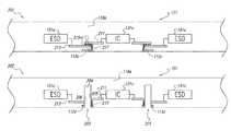
- FIG. 1Ais a cross-sectional side view of a system of stacked microelectronic dies having electrostatic discharge components configured in accordance with an embodiment of the disclosure.
- FIG. 1Bis a schematic view of a system of stacked microelectronic dies in accordance with an embodiment of the disclosure.
- FIGS. 2A-Fillustrate stages of methods for forming the system of FIG. 1A in accordance with several embodiments of the disclosure.
- FIG. 3is a cross-sectional side view of a microelectronic workpiece configured in accordance with another embodiment of the disclosure.
- FIG. 4is a cross-sectional side view of a microelectronic workpiece configured in accordance with yet another embodiment of the disclosure.
- FIG. 5is a schematic illustration of a system in which embodiments of microelectronic dies having electrostatic discharge components with disabled electrical connections may be incorporated.
- interconnectmay encompass various types of conductive structures that extend at least partially through a substrate of a microelectronic die and electrically couple together conductive contacts located at opposing ends of the interconnect.
- substratemay encompass any of a variety of conductive and/or nonconductive layers (e.g., metallic, semi-conductive, and/or dielectric materials) that are situated upon and/or within one another.
- Such substratescan include any of a myriad of electrical devices (e.g., transistors, resistors, capacitors, etc.) or systems of such devices (e.g., an integrated circuit, a memory, a processor, etc.) formed in the conductive and/or nonconductive layers of an individual substrate.
- electrical devicese.g., transistors, resistors, capacitors, etc.
- systems of such devicese.g., an integrated circuit, a memory, a processor, etc.
- Other embodiments of pass-through interconnects, substrates, and microelectronic dies and/or systems of dies that include such interconnects and substratesin addition to or in lieu of the embodiments described in this section, may have several additional features or may not include many of the features shown and described below with reference to FIGS. 1-5 .
- FIG. 1Ais a cross-sectional side view of an embodiment of a system 100 having a first microelectronic die 101 and a second microelectronic die 102 stacked on the first die 101 .
- the first die 101includes a first substrate 110 a , a plurality of pass-through 3D interconnects 120 extending through the first substrate 110 a , and a first integrated circuit 130 a electrically coupled to the interconnects 120 .
- the first substrate 110 acan be a silicon substrate or another suitable semiconductor substrate.
- the first integrated circuit 130 ais shown schematically, and it will be appreciated that the first integrated circuit 130 a is within a large portion of the first substrate 110 a .
- the first die 101can also include a plurality of first substrate pads 112 a located at corresponding interconnects 120 and electrically coupled to the first integrated circuit 130 a .
- the first die 101further includes dielectric liners 122 along the interconnects 120 , a backside dielectric layer 114 defining a backside surface 115 , and a redistribution layer (RDL) 140 having RDL traces 142 with contacts 144 .
- the dielectric liners 122electrically isolate the individual interconnects 120 from the first substrate 110 a and the first substrate pads 112 a
- the RDL traces 142electrically couple the first substrate pads 112 a and the corresponding interconnects 120 to the contacts 144 .
- the second die 102can have a second substrate 110 b with second contact pads 112 b and a front side structure 180 having front side contacts 184 arranged in the pattern of the interconnects 120 of the first die 101 .
- the second die 102can also optionally include a second integrated circuit 130 b electrically coupled to the second substrate pads 112 b .
- the second substrate 110 bcan also be a silicon substrate or another suitable semiconductor substrate, and the second integrated circuit 130 b is also shown schematically and can be within a large portion of the second substrate 110 b .
- metal bonds 166can electrically coupled the front side contacts 184 of the second die 102 to corresponding interconnects 120 of the first die 101 .
- electrical connectorssuch as solder balls, can be used in lieu of the metal bonds 166 .
- FIG. 1Bschematically illustrates an embodiment of the first and second integrated circuits 130 a - b in greater detail.
- the first integrated circuit 130 a of the first die 101can include internal circuitry 131 a and a first electrostatic discharge system 150 a
- the second integrated circuit 130 b of the second die 102can include internal circuitry 131 b and a second electrostatic discharge system 150 b
- the first electrostatic discharge system 150 acan include one or more first electrostatic discharge (ESD) devices 151 a
- the first ESD devices 151 acan include temporary ESD devices and/or permanent ESD devices depending on the application.
- the temporary first ESD devices 151 acan be current ESD devices (ESDi) that are temporarily coupled to the first substrate pad 112 a and power or ground, and the permanent first ESD devices 151 a can be voltage ESD devices (ESDV) coupled to the first substrate pad 112 a via a resistor 153 a and the internal circuitry 131 a .
- the second electrostatic discharge system 150 bcan include one or more second ESD devices 151 b that can include current ESD devices (ESDi) coupled by lines 154 and voltage ESD devices (ESDV) coupled via a resistor 155 b ; in many embodiments all of the second ESD devices 151 b remain electrically coupled to internal circuitry.
- the electrostatic discharge systems 150 a - bhave one or more ESD devices associated with each substrate pad (e.g., one or more current and/or voltage ESD device for each substrate pad).
- selected first ESD devices 151 aare electrically isolated from the other components of the first integrated circuit 130 a at one or more stages of the fabrication process.
- the ESDi deviceshave been electrically isolated from the substrate pad 112 a and interconnect 120 , but ESDV devices remain electrically connected to the internal circuitry 131 a .
- all of the first ESD devices 151 acan be temporary devices that are eventually disconnected from the other components of the first integrated circuit 130 a.
- the selected first ESD devices 151 acan be electrically isolated from the other components of the first integrated circuit 130 a by forming the dielectric liners 122 between the selected first ESD devices 151 a and the interconnects 120 .
- a dielectric liner 122can be formed to cause a break in a line 154 that previously connected a selected first ESD device 151 a to a corresponding first substrate pad 112 a .
- selected first ESD devices 151 acan be effectively disabled or disconnected in the packaged system 100 .
- all of the first ESD devices 151 acan be electrically disconnected or disabled at one or more stages of the fabrication process.
- the second ESD devices 151 bare not electrically isolated from an integrated circuit.
- the second ESD devices 151 bcan remain electrically coupled to the other components of the second integrated circuit 130 b , and the second ESD devices 151 b can also be electrically coupled to the first integrated circuit 130 a via a conductive path that includes an individual contact 184 , a conductive layer 185 , an individual metal bond 166 , and an individual interconnect 120 .
- the second ESD devices 151 bcan be separate components in the second die 102 that are not electrically coupled to the second integrated circuit 130 b.
- the ESD systems 150 a - bare configured to protect an integrated circuit from an ESD event.
- An ESD eventtypically involves the transfer of energy between an integrated circuit and another body that is at a different electrical potential than the integrated circuit.
- an equipment operatorcan inadvertently touch and transfer an electrostatic potential to one of the substrate pads 112 b .
- the transferred electrostatic potentialcan deliver a large electrical charge that could damage charge-sensitive portions of the second integrated circuit 130 b .
- ESD eventscan also be caused by ionized ambient discharges (e.g., sparks) between a substrate pad and other charged bodies brought into close proximity with the substrate pad.
- Embodiments of the ESD systems 150 a - bcan include circuit elements that divert potentially damaging charges away from a corresponding integrated circuit and/or charge-sensitive portions of the integrated circuit.
- individual ESD devicesinclude one or more diodes, metal-oxide-silicon (MOS) devices, and/or silicon-controlled rectifiers (SCRs) that are electrically coupled with a corresponding integrated circuit.
- MOSmetal-oxide-silicon
- SCRssilicon-controlled rectifiers
- the second ESD devices 151 bare components of the second integrated circuit 130 b and in a parallel circuit configuration with the first integrated circuit 130 a .
- disabling the electrical connections associated with the selected first ESD devices 151 acan be carried out when forming the interconnects 120 , and in this case the first ESD devices 151 a that remain electrically coupled to the first integrated circuit can protect the first integrated circuit during formation of the interconnects 120 (e.g., the ESDV devices shown in FIG. 1B ).
- conventional dies in stacked packagestypically have an ESD device dedicated to each connection between a substrate pad and an integrated circuit.
- the ESD devices at one level of the conventional die stackare coupled to the ESD devices at another level of the conventional die stack. This creates multiple levels of ESD devices interconnected with one another. In general, a large number of ESD devices are redundant, and a single ESD device for each group of interconnected substrate pads is sufficient for protecting integrated circuits at all levels of the die stack. Removing or disabling ESD devices from only some of these dies and not others would require that the dies have a different configuration of integrated circuitry. This would accordingly require die manufacturers to fabricate separate workpieces to create the different integrated circuits.
- Embodiments of the system 100overcome the tradeoff between overall performance and manufacturing costs.
- electrical connections with ESD devicescan be disabled at little or no additional cost such that the system 100 does not employ redundant ESD devices.
- the ESD devicescan be selectively disable in the normal process of fabrication interconnects by forming selected interconnects through one or more metal layers, traces, and/or vias that complete the temporary conductive path between an ESD device and an integrated circuit. This process not only forms the interconnect but also removes conductive material to disconnect or otherwise disable the ESD device at the same time.
- electrical isolationcan also be provided by a dielectric layer that separates the interconnect from the substrate.
- Embodiments of the system 100can also include a dielectric casing 198 encapsulating the first and second dies 101 and 102 and an interposer substrate 190 carrying the first and second dies 101 and 102 .
- the interposer substrate 190can be a printed circuit board or other substrate that includes die bond pads 192 and package bond pads 194 electrically coupled to the die bond pads 192 through the interposer substrate 190 .
- individual bump bonds 196 or other electrical connectorsare aligned with and attached to individual RDL contacts 144 of the first die 101 and individual die bond pads 192 of the interposer substrate 190 . Accordingly, individual package bond pads 194 can provide an electrical coupling to the first integrated circuit 130 a of the first die 101 , the second integrated circuit 130 b , and the second ESD devices 151 b of the second die 102 .
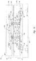
- FIGS. 2A-Fillustrate stages of methods for forming the system 100 and selectively disabling electrical connections with ESD devices in accordance with several embodiments of the disclosure.
- FIG. 2Ais a cross-sectional side view of a microelectronic workpiece 202 (e.g., a semiconductor or microelectronic wafer) at a stage of forming an embodiment of the first die 101 .
- the workpiece 202includes the first substrate 110 a , the internal circuitry 131 a , selected first ESD devices 151 a , and corresponding first substrate pads 112 a .
- FIG. 2Ais a cross-sectional side view of a microelectronic workpiece 202 (e.g., a semiconductor or microelectronic wafer) at a stage of forming an embodiment of the first die 101 .
- the workpiece 202includes the first substrate 110 a , the internal circuitry 131 a , selected first ESD devices 151 a , and corresponding first substrate pads
- the internal circuitry 131 ais electrically coupled to a first metal layer 211 and the first ESD devices 151 a are electrically coupled to a second metal layer 213 .
- the first metal layer 211can be electrically coupled to the second metal layer 213 by conductive vias 215 , and thus the first ESD devices 151 a are electrically coupled to the internal circuitry 131 a at this stage of the process.
- the workpiece 202also includes second vias 217 that electrically couple the internal circuitry 131 a and the first ESD devices 151 a to the first substrate pads 112 a.
- the first metal layer 211 , the second metal layer 213 , the first vias 215 , and the second via 217are formed during a back end of the line (BEOL) process.
- the first and second metal layers 211 and 213can include aluminum, copper, or another metal that has been formed above semiconductor devices (not shown) of the integrated circuit. This metal can be patterned to define electrical connections of the integrated circuit and can include passivation layers (not shown) that separate individual levels of metal from one another.
- the first and second vias 215 and 217can also be formed in a BEOL process and can include a metallic material (e.g., copper or tungsten).
- the vias 215 and 217can extend through individual passivation layers to provide the electrical couplings between (a) the first and second metal layers 211 and 213 and (b) the first metal layer 211 and the first substrate pads 112 a .
- other arrangements of vias or interconnect structurescan be used to interconnect metal layers and substrate pads.
- two or more viascan couple the first metal layer 211 to the substrate pad 144 and/or a single via can couple the first metal layer 211 to the second metal layer 213 .
- the number of vias and interconnect structurescan also be based on the magnitude of a typical electrical current carried by the first metal layer 211 and/or the second metal layer 213 .
- FIG. 2Bis a cross-sectional side view of the workpiece 202 at a subsequent stage after forming holes 203 extending at least partially through the workpiece 202 .
- An individual hole 203is formed through the substrate pad 112 a , and the hole 203 includes an endwall 204 , a first sidewall 205 that is adjacent to the first metal layer 211 , and a second sidewall 206 that is adjacent to the second metal layer 213 .
- an etching processforms the hole 203 using single- or multi-step wet/dry etching techniques, laser drilling/ablation methods and/or silicon machining techniques (e.g., micro-electro-discharge-machining, abrasive machining, sand blasting, and/or cryogenic etches).
- the etching processcan form the holes 203 such that the first vias 215 ( FIG. 2A ) are removed from the workpiece 202 and the selected first ESD devices 151 a are disconnected from the internal circuitry 131 a .
- the etching processdoes not remove the second vias 217 from the workpiece 202 so that the internal circuitry 131 a remains electrically coupled to the substrate pads 112 a .
- the holes 203can be formed other locations in the workpiece 202 to disconnect the selected first ESD device 151 a without removing the first vias 215 .
- an etching processcan form the holes 203 in the second metal layer 213 such that a portion of the second metal layer 213 is removed from the workpiece 202 and the selected first ESD devices 151 a are electrically disconnected from the internal circuitry 131 a.
- FIG. 2Cis a cross-sectional side view of the workpiece 202 at a subsequent stage after forming a dielectric liner 122 along the endwall 204 and the sidewalls 205 and 206 of the hole 203 .
- the dielectric liner 122may initially be globally deposited on the workpiece 202 , and a wet/dry etch can remove portions of the dielectric layer 122 that are not located within the hole 203 .
- the dielectric liner 122includes a nonconductive material that can be deposited at low temperatures, such as materials that can be deposited using chemical vapor and/or physical vapor deposition (CVD and/or PVD) processes.
- the dielectric liner 122can include a phosphosilicate glass (PSG) or other type of organic or inorganic dielectric coating material.
- PSGphosphosilicate glass
- FIG. 2Dis a cross-sectional side view of the workpiece 202 at a subsequent stage after forming the interconnects 120 .
- a seed layer(not shown) can be formed on the surfaces of the dielectric liner 122 within the hole 203 ( FIG. 2C ), and individual metal layers 224 can be plated onto the seed layer.
- the seed layercan be a conductive material, such as copper, and may receive an electrical potential for initiating plating of the metal layer 224 . In other embodiments, however, an electroless plating process can form the metal layer 224 .
- the interconnect 120is shown as being completely filled by the metal layer 224 , in other examples, the interconnect 120 may be only partially filled by the metal layer 224 .
- the interconnect 120can include an opening extending through the center of the metal layer 224 .
- the metal layer 224can include copper, gold, nickel, and/or palladium.
- FIG. 2Eis a cross-sectional side view of the workpiece 202 at a subsequent stage after thinning the first substrate 110 a and depositing the dielectric layer 114 .
- the first substrate 110 acan be thinned using chemical etching, backgrinding, chemical-mechanical polishing, and/or plasma thinning techniques. Such a process can be carried out in single or multiple steps and can also include selectively removing substrate material from the first substrate 110 a to define a projection portion 227 of the interconnect 120 .
- the dielectric layer 114can be deposited at the back-side surface of the first substrate 110 a .
- the dielectric layer 114can be spun-on such that the dielectric layer 114 covers the back-side surface of the first substrate 110 a but does not cover the projection portion of the interconnect 227 .
- an additional etching processcan remove portions of the dielectric liner 122 from the sidewalls of the projection portion 227 using, for example, a dilute hydrofluoric (HF) etch.
- FIG. 2Ealso shows the redistribution layer 140 including the RDL traces 142 , the RDL contacts 144 , and a passivation layer 256 encapsulating the RDL traces 142 and defining locations of the RDL contacts 144 .
- FIG. 2Fis a partially exploded, cross-sectional side view of the workpiece 202 during inter-die bonding and the die singulation stage.
- second die 102is aligned with and electrically connected to the first die 101 by forming the metal bonds 166 between the RDL contacts 184 of the second die 102 and the interconnects 120 of the first die 101 .
- the substrate 110 amay include fiducials or other types of alignment markers for accurate alignment between the RDL contacts 184 and the interconnects 120 , and various types of direct bonding techniques can be employed for forming the metal bonds 166 .
- bonding techniquessuch as copper-to-copper bonding, copper-to-tin bonding, oxide bonding, and electroplating may be used to electrically intercouple the RDL connects 184 with the interconnects 120 .
- the second die 102can also be optionally attached to the first die 101 with an adhesive layer (not shown). After electrically connecting the second die 102 to the first die 101 , the first die 101 can be singulated from the workpiece 202 via a die cutting process at substrate cutting lanes 248 to separate the assembly of the first and second dies 101 and 102 from the workpiece 202 .
- the assembly of the first and second dies 101 and 102can then be mounted and electrically coupled to a variety of substrates, such as the interposer substrate 190 ( FIG. 1A ). In other embodiments, this assembly can be coupled with other types of structures for carrying and/or electrically coupling with the first and second dies 101 and 102 .
- FIG. 3is a cross-sectional side view showing an embodiment of a workpiece 302 carrying internal circuitry 333 , a temporary ESD device 335 a electrically isolated from the internal circuitry 333 , and a permanent ESD device 335 b electrically coupled to the internal circuitry 333 .
- the embodiment shown in FIG. 3can be similar to the first die 101 shown in FIG. 1B .
- the temporary ESD device 335 acan be electrically isolated from the internal circuitry 333 in a similar manner to that described with reference to FIGS. 2A-F .
- the permanent ESD device 335 bcan provide ESD protection to the internal circuitry 333 during subsequent manufacturing of the workpiece 302 .
- the permanent ESD device 335 bhas a smaller footprint than the temporary ESD device 335 a and introduces less signal delay than the temporary ESD device 335 a .
- the permanent ESD device 335 bmay not be as effective at ESD protection as the temporary ESD device 335 a , but the permanent ESD device 335 b can provide a measure of ESD protection during manufacturing between the time when the temporary ESD device 335 a is electrically isolated from the internal circuitry 333 and the time when the internal circuitry 333 is electrically coupled to the second ESD device 335 b of the second die 102 ( FIG. 1A ).
- FIG. 4is a cross-sectional side view showing an embodiment of a workpiece 402 carrying a memory 433 , a first memory component 435 a electrically isolated from the memory 433 , and a second memory component 435 b electrically coupled to the memory 433 .
- the memory 433can be a programmable memory, and the process of forming the interconnect 120 can be used to program the memory 433 by disabling the functionality of the first memory component 435 a .
- Such a programming implementationcan be similar in nature to permanently programming a field programmable gate array (FPGA). However, instead of using electrical potentials to selectively hardwire the memory, the process of forming the interconnect can selectively hardwire the memory 433 .
- FPGAfield programmable gate array
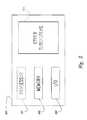
- any one of the microelectronic dies having ESD devices with disabled electrical connections described above with reference to FIGS. 1A-4can be incorporated into any of a myriad of larger or more complex systems 500 , a representative one of which is shown schematically in FIG. 5 .
- the system 500can include a processor 501 , a memory 502 (e.g., SRAM, DRAM, Flash, or other memory device), input/output devices 503 , or other subsystems or components 504 .
- Microelectronic devicesmay be included in any of the components shown in FIG. 5 .
- the resulting system 500can perform any of a wide variety of computing, processing, storage, sensor, imaging, or other functions.
- representative systems 500include, without limitation, computers or other data processors, for example, desktop computers, laptop computers, Internet appliances, hand-held devices (e.g., palm-top computers, wearable computers, cellular or mobile phones, and personal digital assistants), multi-processor systems, processor-based or programmable consumer electronics, network computers, and minicomputers.
- Other representative systems 500include cameras, light or other radiation sensors, servers and associated server subsystems, display devices, or memory devices.
- individual diescan include imager arrays, such as CMOS imagers.
- Components of the system 500may be housed in a single unit or distributed over multiple, interconnected units, e.g., through a communications network. Components can accordingly include local or remote memory storage devices and any of a wide variety of computer-readable media.
- embodiments of the stacked system 100can employ other types of intra-die electrical couplings between dies or between a die and an interposer substrate.
- the described methods of disabling electrical connections to ESD devicescan include various modifications. Referring to FIG. 1A , for example, electrical connections can be disabled at metal layers located within the substrate 140 or at metal layers located within a redistribution layer 140 .
- many of the elements of one embodimentcan be combined with other embodiments in addition to, or in lieu of, the elements of the other embodiments. Accordingly, the invention is not limited except as by the appended claims.
Landscapes
- Engineering & Computer Science (AREA)
- Microelectronics & Electronic Packaging (AREA)
- Power Engineering (AREA)
- Computer Hardware Design (AREA)
- Physics & Mathematics (AREA)
- Condensed Matter Physics & Semiconductors (AREA)
- General Physics & Mathematics (AREA)
- Manufacturing & Machinery (AREA)
- Semiconductor Integrated Circuits (AREA)
- Internal Circuitry In Semiconductor Integrated Circuit Devices (AREA)
Abstract
Description
Claims (14)
Priority Applications (4)
| Application Number | Priority Date | Filing Date | Title |
|---|---|---|---|
| US13/572,461US8404521B2 (en) | 2008-05-15 | 2012-08-10 | Disabling electrical connections using pass-through 3D interconnects and associated systems and methods |
| US13/850,803US8772086B2 (en) | 2008-05-15 | 2013-03-26 | Disabling electrical connections using pass-through 3D interconnects and associated systems and methods |
| US14/324,958US9343368B2 (en) | 2008-05-15 | 2014-07-07 | Disabling electrical connections using pass-through 3D interconnects and associated systems and methods |
| US15/144,065US9607930B2 (en) | 2008-05-15 | 2016-05-02 | Disabling electrical connections using pass-through 3D interconnects and associated systems and methods |
Applications Claiming Priority (2)
| Application Number | Priority Date | Filing Date | Title |
|---|---|---|---|
| US12/121,654US8253230B2 (en) | 2008-05-15 | 2008-05-15 | Disabling electrical connections using pass-through 3D interconnects and associated systems and methods |
| US13/572,461US8404521B2 (en) | 2008-05-15 | 2012-08-10 | Disabling electrical connections using pass-through 3D interconnects and associated systems and methods |
Related Parent Applications (1)
| Application Number | Title | Priority Date | Filing Date |
|---|---|---|---|
| US12/121,654DivisionUS8253230B2 (en) | 2008-05-15 | 2008-05-15 | Disabling electrical connections using pass-through 3D interconnects and associated systems and methods |
Related Child Applications (1)
| Application Number | Title | Priority Date | Filing Date |
|---|---|---|---|
| US13/850,803ContinuationUS8772086B2 (en) | 2008-05-15 | 2013-03-26 | Disabling electrical connections using pass-through 3D interconnects and associated systems and methods |
Publications (2)
| Publication Number | Publication Date |
|---|---|
| US20120309128A1 US20120309128A1 (en) | 2012-12-06 |
| US8404521B2true US8404521B2 (en) | 2013-03-26 |
Family
ID=41315390
Family Applications (5)
| Application Number | Title | Priority Date | Filing Date |
|---|---|---|---|
| US12/121,654Active2029-10-14US8253230B2 (en) | 2008-05-15 | 2008-05-15 | Disabling electrical connections using pass-through 3D interconnects and associated systems and methods |
| US13/572,461ActiveUS8404521B2 (en) | 2008-05-15 | 2012-08-10 | Disabling electrical connections using pass-through 3D interconnects and associated systems and methods |
| US13/850,803ActiveUS8772086B2 (en) | 2008-05-15 | 2013-03-26 | Disabling electrical connections using pass-through 3D interconnects and associated systems and methods |
| US14/324,958ActiveUS9343368B2 (en) | 2008-05-15 | 2014-07-07 | Disabling electrical connections using pass-through 3D interconnects and associated systems and methods |
| US15/144,065ActiveUS9607930B2 (en) | 2008-05-15 | 2016-05-02 | Disabling electrical connections using pass-through 3D interconnects and associated systems and methods |
Family Applications Before (1)
| Application Number | Title | Priority Date | Filing Date |
|---|---|---|---|
| US12/121,654Active2029-10-14US8253230B2 (en) | 2008-05-15 | 2008-05-15 | Disabling electrical connections using pass-through 3D interconnects and associated systems and methods |
Family Applications After (3)
| Application Number | Title | Priority Date | Filing Date |
|---|---|---|---|
| US13/850,803ActiveUS8772086B2 (en) | 2008-05-15 | 2013-03-26 | Disabling electrical connections using pass-through 3D interconnects and associated systems and methods |
| US14/324,958ActiveUS9343368B2 (en) | 2008-05-15 | 2014-07-07 | Disabling electrical connections using pass-through 3D interconnects and associated systems and methods |
| US15/144,065ActiveUS9607930B2 (en) | 2008-05-15 | 2016-05-02 | Disabling electrical connections using pass-through 3D interconnects and associated systems and methods |
Country Status (1)
| Country | Link |
|---|---|
| US (5) | US8253230B2 (en) |
Cited By (3)
| Publication number | Priority date | Publication date | Assignee | Title |
|---|---|---|---|---|
| US20120153437A1 (en)* | 2010-12-20 | 2012-06-21 | National Chiao Tung University | Esd protection structure for 3d ic |
| US20130214421A1 (en)* | 2008-05-15 | 2013-08-22 | Micron Technology, Inc. | Disabling electrical connections using pass-through 3d interconnects and associated systems and methods |
| US9209158B2 (en) | 2007-12-28 | 2015-12-08 | Micron Technology, Inc. | Pass-through 3D interconnect for microelectronic dies and associated systems and methods |
Families Citing this family (108)
| Publication number | Priority date | Publication date | Assignee | Title |
|---|---|---|---|---|
| SG120200A1 (en) | 2004-08-27 | 2006-03-28 | Micron Technology Inc | Slanted vias for electrical circuits on circuit boards and other substrates |
| US7795134B2 (en) | 2005-06-28 | 2010-09-14 | Micron Technology, Inc. | Conductive interconnect structures and formation methods using supercritical fluids |
| US7863187B2 (en) | 2005-09-01 | 2011-01-04 | Micron Technology, Inc. | Microfeature workpieces and methods for forming interconnects in microfeature workpieces |
| US20070045120A1 (en)* | 2005-09-01 | 2007-03-01 | Micron Technology, Inc. | Methods and apparatus for filling features in microfeature workpieces |
| US7262134B2 (en) | 2005-09-01 | 2007-08-28 | Micron Technology, Inc. | Microfeature workpieces and methods for forming interconnects in microfeature workpieces |
| US7629249B2 (en) | 2006-08-28 | 2009-12-08 | Micron Technology, Inc. | Microfeature workpieces having conductive interconnect structures formed by chemically reactive processes, and associated systems and methods |
| US7902643B2 (en) | 2006-08-31 | 2011-03-08 | Micron Technology, Inc. | Microfeature workpieces having interconnects and conductive backplanes, and associated systems and methods |
| SG149710A1 (en) | 2007-07-12 | 2009-02-27 | Micron Technology Inc | Interconnects for packaged semiconductor devices and methods for manufacturing such devices |
| US7884015B2 (en) | 2007-12-06 | 2011-02-08 | Micron Technology, Inc. | Methods for forming interconnects in microelectronic workpieces and microelectronic workpieces formed using such methods |
| US7745920B2 (en) | 2008-06-10 | 2010-06-29 | Micron Technology, Inc. | Packaged microelectronic devices and methods for manufacturing packaged microelectronic devices |
| US8334599B2 (en)* | 2008-08-21 | 2012-12-18 | Qimonda Ag | Electronic device having a chip stack |
| US8455357B2 (en)* | 2008-10-10 | 2013-06-04 | Taiwan Semiconductor Manufacturing Co., Ltd. | Method of plating through wafer vias in a wafer for 3D packaging |
| US8080885B2 (en)* | 2008-11-19 | 2011-12-20 | Stats Chippac Ltd. | Integrated circuit packaging system with multi level contact and method of manufacture thereof |
| JP2010129958A (en)* | 2008-12-01 | 2010-06-10 | Seiko Epson Corp | Semiconductor device, and manufacturing method thereof |
| JP2010135391A (en)* | 2008-12-02 | 2010-06-17 | Seiko Epson Corp | Semiconductor device and method for manufacturing the same |
| US8513119B2 (en) | 2008-12-10 | 2013-08-20 | Taiwan Semiconductor Manufacturing Company, Ltd. | Method of forming bump structure having tapered sidewalls for stacked dies |
| US20100171197A1 (en)* | 2009-01-05 | 2010-07-08 | Hung-Pin Chang | Isolation Structure for Stacked Dies |
| US8232625B2 (en)* | 2009-03-26 | 2012-07-31 | International Business Machines Corporation | ESD network circuit with a through wafer via structure and a method of manufacture |
| KR101069287B1 (en)* | 2009-04-29 | 2011-10-04 | 주식회사 하이닉스반도체 | Semiconductor package and method of manufacturing the same |
| US8054597B2 (en)* | 2009-06-23 | 2011-11-08 | International Business Machines Corporation | Electrostatic discharge structures and methods of manufacture |
| US8148813B2 (en)* | 2009-07-31 | 2012-04-03 | Altera Corporation | Integrated circuit package architecture |
| US8743561B2 (en) | 2009-08-26 | 2014-06-03 | Taiwan Semiconductor Manufacturing Company, Ltd. | Wafer-level molded structure for package assembly |
| US8791549B2 (en) | 2009-09-22 | 2014-07-29 | Taiwan Semiconductor Manufacturing Company, Ltd. | Wafer backside interconnect structure connected to TSVs |
| US8053898B2 (en)* | 2009-10-05 | 2011-11-08 | Samsung Electronics Co., Ltd. | Connection for off-chip electrostatic discharge protection |
| US8951839B2 (en)* | 2010-03-15 | 2015-02-10 | Stats Chippac, Ltd. | Semiconductor device and method of forming conductive vias through interconnect structures and encapsulant of WLCSP |
| US8466059B2 (en) | 2010-03-30 | 2013-06-18 | Taiwan Semiconductor Manufacturing Company, Ltd. | Multi-layer interconnect structure for stacked dies |
| WO2011140082A1 (en)* | 2010-05-03 | 2011-11-10 | Georgia Tech Research Corporation | Cmut devices and fabrication methods |
| TWI427753B (en)* | 2010-05-20 | 2014-02-21 | Advanced Semiconductor Eng | Package structure and package process |
| KR101190744B1 (en) | 2010-05-27 | 2012-10-12 | 에스케이하이닉스 주식회사 | Semiconductor integrated circuit having multi-chip structure |
| KR101211044B1 (en) | 2010-05-27 | 2012-12-12 | 에스케이하이닉스 주식회사 | Semiconductor integrated circuit having multi-chip structure |
| US8754516B2 (en) | 2010-08-26 | 2014-06-17 | Intel Corporation | Bumpless build-up layer package with pre-stacked microelectronic devices |
| KR101690487B1 (en)* | 2010-11-08 | 2016-12-28 | 삼성전자주식회사 | Semiconductor device and fabrication method thereof |
| WO2012125681A2 (en)* | 2011-03-14 | 2012-09-20 | Tufts University | Method to mitigate through-silicon via-induced substrate noise |
| US8803269B2 (en) | 2011-05-05 | 2014-08-12 | Cisco Technology, Inc. | Wafer scale packaging platform for transceivers |
| US8367478B2 (en)* | 2011-06-02 | 2013-02-05 | International Business Machines Corporation | Method and system for internal layer-layer thermal enhancement |
| JP2012256639A (en)* | 2011-06-07 | 2012-12-27 | Toshiba Corp | Semiconductor device manufacturing method |
| US8552518B2 (en)* | 2011-06-09 | 2013-10-08 | Optiz, Inc. | 3D integrated microelectronic assembly with stress reducing interconnects |
| US8900994B2 (en) | 2011-06-09 | 2014-12-02 | Taiwan Semiconductor Manufacturing Company, Ltd. | Method for producing a protective structure |
| KR20130004783A (en) | 2011-07-04 | 2013-01-14 | 삼성전자주식회사 | Stacked semiconductor device including esd protection circuits and method of fabricating the stacked semiconductor device |
| US8730626B2 (en)* | 2011-10-04 | 2014-05-20 | Taiwan Semiconductor Manufacturing Company, Ltd. | Electrostatic discharge protection |
| DE102012101606B4 (en)* | 2011-10-28 | 2024-11-21 | Tdk Electronics Ag | ESD protection component and component with an ESD protection component and an LED |
| US9070700B2 (en)* | 2011-11-04 | 2015-06-30 | Broadcom Corporation | Apparatus for electrostatic discharge protection and noise suppression in circuits |
| US9741645B2 (en)* | 2011-12-21 | 2017-08-22 | Intel Corporation | Dense interconnect with solder cap (DISC) formation with laser ablation and resulting semiconductor structures and packages |
| TWI467736B (en)* | 2012-01-04 | 2015-01-01 | Univ Nat Chiao Tung | Three-dimensional integrated circuit device |
| WO2013118426A1 (en)* | 2012-02-09 | 2013-08-15 | パナソニック株式会社 | Semiconductor device and method for manufacturing same |
| US20130228867A1 (en)* | 2012-03-02 | 2013-09-05 | Kabushiki Kaisha Toshiba | Semiconductor device protected from electrostatic discharge |
| KR101931115B1 (en)* | 2012-07-05 | 2018-12-20 | 삼성전자주식회사 | Semiconductor device and method of forming the same |
| US8692289B2 (en)* | 2012-07-25 | 2014-04-08 | Taiwan Semiconductor Manufacturing Company, Ltd. | Fast turn on silicon controlled rectifiers for ESD protection |
| KR102010909B1 (en)* | 2012-08-30 | 2019-08-14 | 삼성전자주식회사 | Package substrates, semiconductor packages having the package substrates, and methods for fabricating the semiconductor packages |
| JP5543567B2 (en)* | 2012-10-22 | 2014-07-09 | 誠 雫石 | Manufacturing method of semiconductor device |
| US20140175657A1 (en)* | 2012-12-21 | 2014-06-26 | Mihir A. Oka | Methods to improve laser mark contrast on die backside film in embedded die packages |
| US8701496B1 (en)* | 2013-02-27 | 2014-04-22 | Honeywell International Inc. | Systems and methods for a pressure sensor having a two layer die structure |
| US9832883B2 (en) | 2013-04-25 | 2017-11-28 | Intel Corporation | Integrated circuit package substrate |
| US9147663B2 (en) | 2013-05-28 | 2015-09-29 | Intel Corporation | Bridge interconnection with layered interconnect structures |
| US10151647B2 (en) | 2013-06-19 | 2018-12-11 | Honeywell International Inc. | Integrated SOI pressure sensor having silicon stress isolation member |
| US20140374877A1 (en)* | 2013-06-21 | 2014-12-25 | Altera Corporation | Integrated Circuits With On-Die Decoupling Capacitors |
| US9472545B2 (en)* | 2014-01-31 | 2016-10-18 | Taiwan Semiconductor Manufacturing Company Limited | Semiconductor arrangement with electrostatic discharge (ESD) protection |
| US9768147B2 (en) | 2014-02-03 | 2017-09-19 | Micron Technology, Inc. | Thermal pads between stacked semiconductor dies and associated systems and methods |
| US9391110B2 (en)* | 2014-08-13 | 2016-07-12 | Taiwan Semiconductor Manufacturing Company, Ltd. | Wafer on wafer stack method of forming and method of using the same |
| US9373585B2 (en)* | 2014-09-17 | 2016-06-21 | Invensas Corporation | Polymer member based interconnect |
| TWI581325B (en)* | 2014-11-12 | 2017-05-01 | 精材科技股份有限公司 | Chip package and manufacturing method thereof |
| US11069734B2 (en) | 2014-12-11 | 2021-07-20 | Invensas Corporation | Image sensor device |
| US9922970B2 (en)* | 2015-02-13 | 2018-03-20 | Qualcomm Incorporated | Interposer having stacked devices |
| US9666514B2 (en) | 2015-04-14 | 2017-05-30 | Invensas Corporation | High performance compliant substrate |
| US9741620B2 (en)* | 2015-06-24 | 2017-08-22 | Invensas Corporation | Structures and methods for reliable packages |
| WO2017048219A1 (en)* | 2015-09-14 | 2017-03-23 | Intel IP Corporation | Advanced node cost reduction by esd interposer |
| US9818726B2 (en)* | 2015-12-28 | 2017-11-14 | International Business Machines Corporation | Chip stack cooling structure |
| US10074731B2 (en)* | 2016-03-07 | 2018-09-11 | Taiwan Semiconductor Manufacturing Co., Ltd | Method for forming semiconductor device structure |
| US10411006B2 (en)* | 2016-05-09 | 2019-09-10 | Infineon Technologies Ag | Poly silicon based interface protection |
| US10204893B2 (en) | 2016-05-19 | 2019-02-12 | Invensas Bonding Technologies, Inc. | Stacked dies and methods for forming bonded structures |
| US20180005887A1 (en)* | 2016-06-30 | 2018-01-04 | International Business Machines Corporation | Through-silicon via with injection molded fill |
| US10325906B2 (en)* | 2016-09-23 | 2019-06-18 | Taiwan Semiconductor Manufacturing Company, Ltd. | ESD testing structure, method of using same and method of forming same |
| DE102016118709B3 (en)* | 2016-10-04 | 2018-01-25 | Infineon Technologies Ag | PROTECTION DEVICE BEFORE ELECTROSTATIC DISCHARGE AND ELECTRONIC SWITCHING DEVICE |
| JP6658441B2 (en)* | 2016-10-06 | 2020-03-04 | 三菱電機株式会社 | Semiconductor device |
| US10593563B2 (en)* | 2017-04-13 | 2020-03-17 | Invensas Corporation | Fan-out wafer level package with resist vias |
| US10879212B2 (en) | 2017-05-11 | 2020-12-29 | Invensas Bonding Technologies, Inc. | Processed stacked dies |
| US10217720B2 (en) | 2017-06-15 | 2019-02-26 | Invensas Corporation | Multi-chip modules formed using wafer-level processing of a reconstitute wafer |
| CN112164688B (en)* | 2017-07-21 | 2023-06-13 | 联华电子股份有限公司 | Chip stacking structure and manufacturing method of chip stacking structure |
| US10128229B1 (en) | 2017-11-13 | 2018-11-13 | Micron Technology, Inc. | Semiconductor devices with package-level configurability |
| US10283462B1 (en) | 2017-11-13 | 2019-05-07 | Micron Technology, Inc. | Semiconductor devices with post-probe configurability |
| TWI672791B (en) | 2018-05-07 | 2019-09-21 | 財團法人工業技術研究院 | Chip package structure and manufacturing method thereof |
| US11276676B2 (en) | 2018-05-15 | 2022-03-15 | Invensas Bonding Technologies, Inc. | Stacked devices and methods of fabrication |
| US10483241B1 (en) | 2018-06-27 | 2019-11-19 | Micron Technology, Inc. | Semiconductor devices with through silicon vias and package-level configurability |
| US11158606B2 (en) | 2018-07-06 | 2021-10-26 | Invensas Bonding Technologies, Inc. | Molded direct bonded and interconnected stack |
| US11462419B2 (en) | 2018-07-06 | 2022-10-04 | Invensas Bonding Technologies, Inc. | Microelectronic assemblies |
| US20200058646A1 (en)* | 2018-08-14 | 2020-02-20 | Intel Corporation | Structures and methods for large integrated circuit dies |
| US10867991B2 (en)* | 2018-12-27 | 2020-12-15 | Micron Technology, Inc. | Semiconductor devices with package-level configurability |
| US10978426B2 (en)* | 2018-12-31 | 2021-04-13 | Micron Technology, Inc. | Semiconductor packages with pass-through clock traces and associated systems and methods |
| CN113330557A (en) | 2019-01-14 | 2021-08-31 | 伊文萨思粘合技术公司 | Bonding structure |
| US11296053B2 (en) | 2019-06-26 | 2022-04-05 | Invensas Bonding Technologies, Inc. | Direct bonded stack structures for increased reliability and improved yield in microelectronics |
| CN110491851A (en)* | 2019-08-22 | 2019-11-22 | 武汉新芯集成电路制造有限公司 | First wafer and forming method thereof, stacked wafer structure |
| US11211348B2 (en) | 2019-08-22 | 2021-12-28 | Wuhan Xinxin Semiconductor Manufacturing Co., Ltd. | First wafer, fabricating method thereof and wafer stack |
| US20210098987A1 (en)* | 2019-09-26 | 2021-04-01 | Priya Walimbe | Electrostatic discharge protection for stacked-die system |
| US12080672B2 (en) | 2019-09-26 | 2024-09-03 | Adeia Semiconductor Bonding Technologies Inc. | Direct gang bonding methods including directly bonding first element to second element to form bonded structure without adhesive |
| US11804479B2 (en)* | 2019-09-27 | 2023-10-31 | Advanced Micro Devices, Inc. | Scheme for enabling die reuse in 3D stacked products |
| US11393790B2 (en)* | 2019-12-06 | 2022-07-19 | Micron Technology, Inc. | Memory with TSV health monitor circuitry |
| US11264373B2 (en) | 2019-12-21 | 2022-03-01 | Intel Corporation | Die backend diodes for electrostatic discharge (ESD) protection |
| US11424239B2 (en)* | 2019-12-21 | 2022-08-23 | Intel Corporation | Diodes for package substrate electrostatic discharge (ESD) protection |
| DE102021101251A1 (en)* | 2020-03-31 | 2021-09-30 | Taiwan Semiconductor Manufacturing Co., Ltd. | PROTECTION AGAINST ANTENNA EFFECTS AND PROTECTION AGAINST ELECTROSTATIC DISCHARGE FOR THREE-DIMENSIONAL INTEGRATED CIRCUITS |
| US11616052B2 (en)* | 2020-04-23 | 2023-03-28 | Innolux Corporation | Method for manufacturing electronic device with ESD protection unit |
| US11631647B2 (en) | 2020-06-30 | 2023-04-18 | Adeia Semiconductor Bonding Technologies Inc. | Integrated device packages with integrated device die and dummy element |
| US11728273B2 (en) | 2020-09-04 | 2023-08-15 | Adeia Semiconductor Bonding Technologies Inc. | Bonded structure with interconnect structure |
| US11764177B2 (en) | 2020-09-04 | 2023-09-19 | Adeia Semiconductor Bonding Technologies Inc. | Bonded structure with interconnect structure |
| US20220199449A1 (en)* | 2020-12-23 | 2022-06-23 | Intel Corporation | Carrier for microelectronic assemblies having direct bonding |
| US12142510B2 (en) | 2020-12-23 | 2024-11-12 | Intel Corporation | Carrier for microelectronic assemblies having direct bonding |
| US11855076B2 (en)* | 2021-01-15 | 2023-12-26 | Taiwan Semiconductor Manufacturing Co., Ltd. | Electrostatic discharge (ESD) array with back end of line (BEOL) connection in a carrier wafer |
| KR20230027833A (en)* | 2021-08-20 | 2023-02-28 | 에스케이하이닉스 주식회사 | Semiconductor Device Including Re-distribution Pads Disposed at Different Levels and A method of Manufacturing the Same |
| US11848278B2 (en)* | 2021-10-14 | 2023-12-19 | Nanya Technology Corporation | Package device comprising electrostatic discharge protection element |
Citations (144)
| Publication number | Priority date | Publication date | Assignee | Title |
|---|---|---|---|---|
| US5145099A (en) | 1990-07-13 | 1992-09-08 | Micron Technology, Inc. | Method for combining die attach and lead bond in the assembly of a semiconductor package |
| US5233448A (en) | 1992-05-04 | 1993-08-03 | Industrial Technology Research Institute | Method of manufacturing a liquid crystal display panel including photoconductive electrostatic protection |
| US5654221A (en) | 1994-10-17 | 1997-08-05 | International Business Machines Corporation | Method for forming semiconductor chip and electronic module with integrated surface interconnects/components |
| US5776824A (en) | 1995-12-22 | 1998-07-07 | Micron Technology, Inc. | Method for producing laminated film/metal structures for known good die ("KG") applications |
| US5821532A (en) | 1997-06-16 | 1998-10-13 | Eastman Kodak Company | Imager package substrate |
| US5851845A (en) | 1995-12-18 | 1998-12-22 | Micron Technology, Inc. | Process for packaging a semiconductor die using dicing and testing |
| US6008070A (en) | 1998-05-21 | 1999-12-28 | Micron Technology, Inc. | Wafer level fabrication and assembly of chip scale packages |
| US6097087A (en) | 1997-10-31 | 2000-08-01 | Micron Technology, Inc. | Semiconductor package including flex circuit, interconnects and dense array external contacts |
| US6103547A (en) | 1997-01-17 | 2000-08-15 | Micron Technology, Inc. | High speed IC package configuration |
| US6114240A (en) | 1997-12-18 | 2000-09-05 | Micron Technology, Inc. | Method for fabricating semiconductor components using focused laser beam |
| US6124634A (en) | 1996-03-07 | 2000-09-26 | Micron Technology, Inc. | Micromachined chip scale package |
| US6159764A (en) | 1997-07-02 | 2000-12-12 | Micron Technology, Inc. | Varied-thickness heat sink for integrated circuit (IC) packages and method of fabricating IC packages |
| US6184465B1 (en) | 1998-11-12 | 2001-02-06 | Micron Technology, Inc. | Semiconductor package |
| US20010000013A1 (en) | 1999-03-01 | 2001-03-15 | Mou-Shiung Lin | High performance sub-system design and assembly |
| US6222270B1 (en) | 1997-06-24 | 2001-04-24 | Samsung Electronics Co., Ltd. | Integrated circuit bonding pads including closed vias and closed conductive patterns |
| US6228687B1 (en) | 1999-06-28 | 2001-05-08 | Micron Technology, Inc. | Wafer-level package and methods of fabricating |
| US6229202B1 (en) | 2000-01-10 | 2001-05-08 | Micron Technology, Inc. | Semiconductor package having downset leadframe for reducing package bow |
| US6246108B1 (en) | 1997-09-15 | 2001-06-12 | Micron Technology, Inc. | Integrated circuit package including lead frame with electrically isolated alignment feature |
| US6271580B1 (en) | 1996-12-30 | 2001-08-07 | Micron Technology, Inc. | Leads under chip in conventional IC package |
| US6291894B1 (en) | 1998-08-31 | 2001-09-18 | Micron Technology, Inc. | Method and apparatus for a semiconductor package for vertical surface mounting |
| US6294837B1 (en) | 1997-12-18 | 2001-09-25 | Micron Technology, Inc. | Semiconductor interconnect having laser machined contacts |
| KR20020022122A (en) | 2000-07-27 | 2002-03-25 | 크리스띠앙 쥘랭 | Process for fabricating a multilevel circuitry comprising tracks and microvias |
| US20020130390A1 (en) | 2001-03-13 | 2002-09-19 | Ming-Dou Ker | ESD protection circuit with very low input capacitance for high-frequency I/O ports |
| US6576531B2 (en) | 2001-08-24 | 2003-06-10 | Micron Technology, Inc. | Method for cutting semiconductor wafers |
| US6582992B2 (en) | 2001-11-16 | 2003-06-24 | Micron Technology, Inc. | Stackable semiconductor package and wafer level fabrication method |
| US6620731B1 (en) | 1997-12-18 | 2003-09-16 | Micron Technology, Inc. | Method for fabricating semiconductor components and interconnects with contacts on opposing sides |
| US20030199119A1 (en) | 1999-03-01 | 2003-10-23 | Megic Corporation | High performance sub-system design and assembly |
| US20030216023A1 (en) | 1997-03-26 | 2003-11-20 | Wark James M. | Projected contact structures for engaging bumped semiconductor devices and methods of making the same |
| US20040043607A1 (en) | 2002-08-29 | 2004-03-04 | Farnworth Warren M. | Methods for creating electrophoretically insulated vias in semiconductive substrates and resulting structures |
| US20040041261A1 (en) | 2002-08-29 | 2004-03-04 | Kinsman Larry D. | Flip-chip image sensor packages and methods of fabrication |
| US6774486B2 (en) | 2001-10-10 | 2004-08-10 | Micron Technology, Inc. | Circuit boards containing vias and methods for producing same |
| US20040178491A1 (en) | 1997-12-18 | 2004-09-16 | Salman Akram | Method for fabricating semiconductor components by forming conductive members using solder |
| US20040198033A1 (en) | 2002-08-20 | 2004-10-07 | Lee Teck Kheng | Double bumping of flexible substrate for first and second level interconnects |
| US6809025B2 (en) | 1997-02-18 | 2004-10-26 | Micron Technology, Inc. | Method of making a void-free aluminum film |
| US6828175B2 (en) | 2002-08-29 | 2004-12-07 | Micron Technology, Inc. | Semiconductor component with backside contacts and method of fabrication |
| US6858891B2 (en) | 2002-03-06 | 2005-02-22 | Micron Technology, Inc. | Nanotube semiconductor devices and methods for making the same |
| US20050046002A1 (en) | 2003-08-26 | 2005-03-03 | Kang-Wook Lee | Chip stack package and manufacturing method thereof |
| US20050069782A1 (en) | 2003-09-26 | 2005-03-31 | Flip Chip Technologies, L.L.C. | Forming partial-depth features in polymer film |
| WO2005036940A1 (en) | 2003-10-09 | 2005-04-21 | Qualcomm Incorporated | Telescoping blind via in three-layer core |
| US20050104228A1 (en) | 2003-11-13 | 2005-05-19 | Rigg Sidney B. | Microelectronic devices, methods for forming vias in microelectronic devices, and methods for packaging microelectronic devices |
| US20050110095A1 (en) | 2003-11-20 | 2005-05-26 | Taiwan Semiconductor Manufacturing Co. | Novel stacked string for power protection and power connection |
| US20050110889A1 (en) | 2003-11-26 | 2005-05-26 | Tuttle Mark E. | Packaged microelectronic imagers and methods of packaging microelectronic imagers |
| US20050127478A1 (en) | 2003-12-10 | 2005-06-16 | Hiatt William M. | Microelectronic devices and methods for filling vias in microelectronic devices |
| US6913952B2 (en) | 2003-07-03 | 2005-07-05 | Micron Technology, Inc. | Methods of forming circuit traces and contact pads for interposers utilized in semiconductor packages |
| US20050150683A1 (en) | 2004-01-12 | 2005-07-14 | Farnworth Warren M. | Methods of fabricating substrates and substrate precursor structures resulting therefrom |
| US20050164500A1 (en) | 2002-08-13 | 2005-07-28 | Lindgren Joseph T. | Selective passivation of exposed silicon |
| US20050184219A1 (en) | 2004-02-23 | 2005-08-25 | Kirby Kyle K. | Packaged microelectronic imagers and methods of packaging microelectronic imagers |
| US6946325B2 (en) | 2003-03-14 | 2005-09-20 | Micron Technology, Inc. | Methods for packaging microelectronic devices |
| US20050208766A1 (en) | 2004-03-19 | 2005-09-22 | Kirby Kyle K | Etch solution for selectively removing silicon and methods of selectively removing silicon |
| US20050227382A1 (en) | 2004-04-02 | 2005-10-13 | Hui Angela T | In-situ surface treatment for memory cell formation |
| US20050236708A1 (en) | 2004-04-27 | 2005-10-27 | Farnworth Warren M | Microelectronic imaging devices and methods of packaging microelectronic imaging devices |
| US20050247894A1 (en) | 2004-05-05 | 2005-11-10 | Watkins Charles M | Systems and methods for forming apertures in microfeature workpieces |
| US20050254133A1 (en) | 2004-05-13 | 2005-11-17 | Salman Akram | Integrated optics units and methods of manufacturing integrated optics units for use with microelectronic imagers |
| US20050253213A1 (en) | 2004-05-13 | 2005-11-17 | Tongbi Jiang | Covers for microelectronic imagers and methods for wafer-level packaging of microelectronics imagers |
| US20050275049A1 (en) | 2004-06-10 | 2005-12-15 | Kirby Kyle K | Packaged microelectronic imagers and methods of packging microelectronic imagers |
| US20050275750A1 (en) | 2004-06-09 | 2005-12-15 | Salman Akram | Wafer-level packaged microelectronic imagers and processes for wafer-level packaging |
| US20050275051A1 (en) | 2004-06-14 | 2005-12-15 | Farnworth Warren M | Prefabricated housings for microelectronic imagers and methods for packaging microelectronic imagers |
| US20050275048A1 (en) | 2004-06-14 | 2005-12-15 | Farnworth Warren M | Microelectronic imagers and methods of packaging microelectronic imagers |
| US20050285154A1 (en) | 2004-06-29 | 2005-12-29 | Salman Akram | Packaged microelectronic imagers and methods of packaging microelectronic imagers |
| US20060014313A1 (en) | 2004-07-16 | 2006-01-19 | Hall Frank L | Microelectronic imaging units and methods of manufacturing microelectronic imaging units |
| US20060011809A1 (en) | 2004-07-19 | 2006-01-19 | Farnworth Warren M | Microelectronic imagers with optical devices and methods of manufacturing such microelectronic imagers |
| US20060024856A1 (en) | 2004-07-28 | 2006-02-02 | Derderian James M | Microelectronic imaging units and methods of manufacturing microelectronic imaging units |
| US20060023107A1 (en) | 2004-08-02 | 2006-02-02 | Bolken Todd O | Microelectronic imagers with optics supports having threadless interfaces and methods for manufacturing such microelectronic imagers |
| US20060035415A1 (en) | 2004-08-16 | 2006-02-16 | Wood Alan G | Frame structure and semiconductor attach process for use therewith for fabrication of image sensor packages and the like, and resulting packages |
| US20060035402A1 (en) | 2004-08-10 | 2006-02-16 | Street Bret K | Microelectronic imaging units and methods of manufacturing microelectronic imaging units |
| US20060040421A1 (en) | 2004-08-19 | 2006-02-23 | Farnworth Warren M | Spacers for packaged microelectronic imagers and methods of making and using spacers for wafer-level packaging of imagers |
| US20060040428A1 (en) | 2004-08-19 | 2006-02-23 | Johnson Mark S | Conductive structures for microfeature devices and methods for fabricating microfeature devices |
| US20060038183A1 (en) | 2004-08-19 | 2006-02-23 | Oliver Steven D | Microelectronic imagers with curved image sensors and methods for manufacturing microelectronic imagers |
| US20060046468A1 (en) | 2004-08-31 | 2006-03-02 | Salman Akram | Through-substrate interconnect fabrication methods and resulting structures and assemblies |
| US20060043509A1 (en) | 2004-08-24 | 2006-03-02 | Watkins Charles M | Packaged microelectronic imaging devices and methods of packaging microelectronic imaging devices |
| US20060046438A1 (en) | 2004-08-31 | 2006-03-02 | Kirby Kyle K | Wafer reinforcement structure and methods of fabrication |
| US20060043262A1 (en) | 2004-08-30 | 2006-03-02 | Micron Technology, Inc. | Microelectronic imagers with integrated optical devices and methods for manufacturing such microelectronic imagers |
| US20060046332A1 (en) | 2004-08-26 | 2006-03-02 | Derderian James M | Microelectronic Imaging units and methods of manufacturing microelectronic imaging units |
| US20060043535A1 (en) | 2004-08-24 | 2006-03-02 | Hiatt William M | Pass through via technology for use during the manufacture of a semiconductor device |
| US20060043569A1 (en) | 2004-08-27 | 2006-03-02 | Benson Peter A | Low temperature methods of forming back side redistribution layers in association with through wafer interconnects, semiconductor devices including same, and assemblies |
| US20060043512A1 (en) | 2004-08-24 | 2006-03-02 | Oliver Steven D | Microelectronic imagers with optical devices having integral reference features and methods for manufacturing such microelectronic imagers |
| US20060044433A1 (en) | 2004-08-31 | 2006-03-02 | Micron Technology, Inc. | Microelectronic imagers having front side contacts and methods of packaging such microelectronic imagers |
| US20060046471A1 (en) | 2004-08-27 | 2006-03-02 | Kirby Kyle K | Methods for forming vias of varying lateral dimensions and semiconductor components and assemblies including same |
| US20060042952A1 (en) | 2004-08-24 | 2006-03-02 | Oliver Steven D | Methods for forming interconnects in vias and microelectronic workpieces including such interconnects |
| US7023090B2 (en) | 2003-01-29 | 2006-04-04 | Taiwan Semiconductor Manufacturing Company, Ltd. | Bonding pad and via structure design |
| US7037836B2 (en) | 2002-12-16 | 2006-05-02 | Dongbuanam Semiconductor Inc. | Method of manufacturing a semiconductor device without oxidized copper layer |
| WO2006053036A2 (en) | 2004-11-10 | 2006-05-18 | Unitive International Limited | Non-circular via holes for bumping pads and related structures |
| US20060148250A1 (en)* | 2004-12-30 | 2006-07-06 | Micron Technology, Inc. | Methods for forming interconnects in microelectronic workpieces and microelectronic workpieces formed using such methods |
| US20060151880A1 (en) | 2005-01-10 | 2006-07-13 | Micron Technology, Inc. | Interconnect structures with bond-pads and methods of forming bump sites on bond-pads |
| US20060154153A1 (en) | 2005-01-10 | 2006-07-13 | Taiwan Semiconductor Manufacturing Co., Ltd. | Anti-ESD photomask blank |
| US7084073B2 (en) | 2002-11-12 | 2006-08-01 | Samsung Electronics Co., Ltd. | Method of forming a via hole through a glass wafer |
| US7083425B2 (en) | 2004-08-27 | 2006-08-01 | Micron Technology, Inc. | Slanted vias for electrical circuits on circuit boards and other substrates |
| US20060177999A1 (en) | 2005-02-10 | 2006-08-10 | Micron Technology, Inc. | Microelectronic workpieces and methods for forming interconnects in microelectronic workpieces |
| US20060177959A1 (en) | 2005-02-10 | 2006-08-10 | Micron Technology, Inc. | Microfeature workpieces having microlenses and methods of forming microlenses on microfeature workpieces |
| US20060180941A1 (en) | 2004-08-31 | 2006-08-17 | Kirby Kyle K | Substrate, semiconductor die, multichip module, and system including a via structure comprising a plurality of conductive elements |
| US20060186492A1 (en) | 2005-02-18 | 2006-08-24 | Micron Technology, Inc. | Microelectronic imagers with shaped image sensors and methods for manufacturing microelectronic imagers |
| US20060199363A1 (en) | 2004-06-29 | 2006-09-07 | Micron Technology, Inc. | Microelectronic devices and methods for forming interconnects in microelectronic devices |
| US20060208360A1 (en) | 2005-03-17 | 2006-09-21 | Taiwan Semiconductor Manufacturing Co., Ltd. | Top via pattern for bond pad structure |
| US20060270108A1 (en) | 2003-03-31 | 2006-11-30 | Farnworth Warren M | Method for fabricating semiconductor components with thinned substrate, circuit side contacts, conductive vias and backside contacts |
| US20060292877A1 (en) | 2005-06-28 | 2006-12-28 | Lake Rickie C | Semiconductor substrates including vias of nonuniform cross section, methods of forming and associated structures |
| US20060290001A1 (en) | 2005-06-28 | 2006-12-28 | Micron Technology, Inc. | Interconnect vias and associated methods of formation |
| US20060289968A1 (en) | 2005-06-28 | 2006-12-28 | Micron Technology, Inc. | Conductive interconnect structures and formation methods using supercritical fluids |
| US20070004079A1 (en) | 2005-06-30 | 2007-01-04 | Geefay Frank S | Method for making contact through via contact to an offset contactor inside a cap for the wafer level packaging of FBAR chips |
| US7164565B2 (en) | 2002-11-29 | 2007-01-16 | Sigmatel, Inc. | ESD protection circuit |
| US20070032061A1 (en) | 2005-08-05 | 2007-02-08 | Farnworth Warren M | Methods of forming through-wafer interconnects and structures resulting therefrom |
| US7183653B2 (en) | 2003-12-17 | 2007-02-27 | Intel Corporation | Via including multiple electrical paths |
| US20070045826A1 (en) | 2005-09-01 | 2007-03-01 | Micron Technology, Inc. | Microfeature workpiece substrates having through-substrate vias, and associated methods of formation |
| US20070045388A1 (en) | 2005-08-31 | 2007-03-01 | Micron Technology, Inc. | Microfeature workpieces having alloyed conductive structures, and associated methods |
| US20070045632A1 (en) | 2005-09-01 | 2007-03-01 | Micron Technology, Inc. | Microelectronic imaging units and methods of manufacturing microelectronic imaging units at the wafer level |
| US20070045779A1 (en) | 2005-09-01 | 2007-03-01 | Hiatt W M | Methods for forming through-wafer interconnects, intermediate structures so formed, and devices and systems having at least one solder dam structure |
| US20070048994A1 (en) | 2005-09-01 | 2007-03-01 | Tuttle Mark E | Methods for forming through-wafer interconnects and structures resulting therefrom |
| US20070045515A1 (en) | 2005-09-01 | 2007-03-01 | Micron Technology, Inc. | Microelectronic imaging devices and associated methods for attaching transmissive elements |
| US20070045834A1 (en) | 2005-08-31 | 2007-03-01 | Micron Technology, Inc. | Interconnecting substrates for microelectronic dies, methods for forming vias in such substrates, and methods for packaging microelectronic devices |
| US20070049016A1 (en) | 2005-09-01 | 2007-03-01 | Micron Technology, Inc. | Microfeature workpieces and methods for forming interconnects in microfeature workpieces |
| US20070045812A1 (en) | 2005-08-31 | 2007-03-01 | Micron Technology, Inc. | Microfeature assemblies including interconnect structures and methods for forming such interconnect structures |
| US20070048896A1 (en) | 2005-08-30 | 2007-03-01 | International Business Machines Corporation | Conductive through via structure and process for electronic device carriers |
| US7190061B2 (en) | 2003-01-03 | 2007-03-13 | Samsung Electronics Co., Ltd. | stack package made of chip scale packages |
| US20070057028A1 (en) | 2005-08-30 | 2007-03-15 | Micron Technology, Inc. | Systems and methods for depositing conductive material into openings in microfeature workpieces |
| US20070077753A1 (en) | 2004-09-09 | 2007-04-05 | Iwatake Michael M | Fabrication of via contacts having dual silicide layers |
| US7217596B2 (en) | 2002-05-08 | 2007-05-15 | Micron Technology, Inc. | Stacked die module and techniques for forming a stacked die module |
| US7217888B2 (en) | 2002-11-26 | 2007-05-15 | Shinko Electric Industries Co., Ltd. | Electronic parts packaging structure and method of manufacturing the same |
| US20070126091A1 (en) | 2005-12-07 | 2007-06-07 | Wood Alan G | Semiconductor components having through wire interconnects (TWI) |
| US20070152342A1 (en) | 2005-12-30 | 2007-07-05 | Taiwan Semiconductor Manufacturing Co., Ltd. | Via structure and process for forming the same |
| US20070158853A1 (en) | 2002-10-09 | 2007-07-12 | Micron Technology, Inc. | Device with novel conductive via structure |
| US20070166991A1 (en) | 2003-09-23 | 2007-07-19 | Nishant Sinha | Methods for forming conductive vias in semiconductor device components |
| US20070170574A1 (en) | 2006-01-25 | 2007-07-26 | Teledyne Licensing, Llc | Buried via technology for three dimensional integrated circuits |
| US20070190803A1 (en) | 2004-05-21 | 2007-08-16 | Agere Systems Inc. | Device and method to eliminate shorting induced by via to metal misalignment |
| US20070197013A1 (en) | 2005-06-14 | 2007-08-23 | Cubic Wafer, Inc. | Processed Wafer Via |
| US7262134B2 (en) | 2005-09-01 | 2007-08-28 | Micron Technology, Inc. | Microfeature workpieces and methods for forming interconnects in microfeature workpieces |
| US20070202617A1 (en) | 2005-04-08 | 2007-08-30 | Hembree David R | Method for fabricating stacked semiconductor components with through wire interconnects |
| US20070222050A1 (en) | 2006-03-17 | 2007-09-27 | Seung Hyun Lee | Stack package utilizing through vias and re-distribution lines |
| US7300857B2 (en) | 2004-09-02 | 2007-11-27 | Micron Technology, Inc. | Through-wafer interconnects for photoimager and memory wafers |
| US20080050904A1 (en) | 2006-08-28 | 2008-02-28 | Micron Technology, Inc. | Methods for attaching microfeature dies to external devices |
| US20080050911A1 (en) | 2006-08-28 | 2008-02-28 | Micron Technology, Inc. | Microfeature workpieces having conductive interconnect structures formed by chemically reactive processes, and associated systems and methods |
| US20080054444A1 (en)* | 2006-08-31 | 2008-03-06 | Micron Technology, Inc. | Microfeature workpieces having interconnects and conductive backplanes, and associated systems and methods |
| US20080057620A1 (en) | 2006-08-30 | 2008-03-06 | Micron Technology, Inc. | Redistribution layers for microfeature workpieces, and associated systems and methods |
| US20080081398A1 (en) | 2006-10-02 | 2008-04-03 | Fionix Inc. | Cap Wafer for Wafer Bonded Packaging and Method for Manufacturing the Same |
| US20080150089A1 (en) | 2006-11-06 | 2008-06-26 | Yong-Chai Kwon | Semiconductor device having through vias and method of manufacturing the same |
| US20090007934A1 (en) | 2007-07-06 | 2009-01-08 | Micron Technology, Inc. | Systems and methods for exposing semiconductor workpieces to vapors for through-hole cleaning and/or other processes |
| US20090014859A1 (en) | 2007-07-12 | 2009-01-15 | Micron Technology, Inc. | Interconnects for packaged semiconductor devices and methods for manufacturing such devices |
| US20090057912A1 (en) | 2007-08-31 | 2009-03-05 | Micron Technology, Inc. | Partitioned through-layer via and associated systems and methods |
| US20090146312A1 (en) | 2007-12-06 | 2009-06-11 | Micron Technology, Inc. | Methods for forming interconnects in microelectronic workpieces and microelectronic workpieces formed using such methods |
| US20090166846A1 (en) | 2007-12-28 | 2009-07-02 | Micron Technology, Inc. | Pass-through 3d interconnect for microelectronic dies and associated systems and methods |
| US20090243045A1 (en)* | 2008-03-27 | 2009-10-01 | Stats Chippac, Ltd. | Through Hole Vias at Saw Streets Including Protrusions or Recesses for Interconnection |
| US20090283898A1 (en) | 2008-05-15 | 2009-11-19 | Janzen Jeffery W | Disabling electrical connections using pass-through 3d interconnects and associated systems and methods |
| US20090315154A1 (en) | 2008-06-19 | 2009-12-24 | Micron Technology, Inc. | Semiconductor with through-substrate interconnect |
| US20090321947A1 (en) | 2008-06-27 | 2009-12-31 | Micron Technology, Inc. | Surface depressions for die-to-die interconnects and associated systems and methods |
| US20100096759A1 (en) | 2008-10-16 | 2010-04-22 | Micron Technology, Inc. | Semiconductor substrates with unitary vias and via terminals, and associated systems and methods |
| US7808075B1 (en)* | 2006-02-07 | 2010-10-05 | Marvell International Ltd. | Integrated circuit devices with ESD and I/O protection |
Family Cites Families (5)
| Publication number | Priority date | Publication date | Assignee | Title |
|---|---|---|---|---|
| US5644167A (en)* | 1996-03-01 | 1997-07-01 | National Semiconductor Corporation | Integrated circuit package assemblies including an electrostatic discharge interposer |
| DE10120408B4 (en)* | 2001-04-25 | 2006-02-02 | Infineon Technologies Ag | Electronic component with a semiconductor chip, electronic assembly of stacked semiconductor chips and method for their production |
| JP4105524B2 (en)* | 2002-10-23 | 2008-06-25 | 株式会社東芝 | Semiconductor device |
| US8367471B2 (en)* | 2007-06-15 | 2013-02-05 | Micron Technology, Inc. | Semiconductor assemblies, stacked semiconductor devices, and methods of manufacturing semiconductor assemblies and stacked semiconductor devices |
| US7968431B2 (en)* | 2008-07-15 | 2011-06-28 | Taiwan Semiconductor Manufacturing Company, Ltd. | Diffusion region routing for narrow scribe-line devices |
- 2008
- 2008-05-15USUS12/121,654patent/US8253230B2/enactiveActive
- 2012
- 2012-08-10USUS13/572,461patent/US8404521B2/enactiveActive
- 2013
- 2013-03-26USUS13/850,803patent/US8772086B2/enactiveActive
- 2014
- 2014-07-07USUS14/324,958patent/US9343368B2/enactiveActive
- 2016
- 2016-05-02USUS15/144,065patent/US9607930B2/enactiveActive
Patent Citations (164)
| Publication number | Priority date | Publication date | Assignee | Title |
|---|---|---|---|---|
| US5145099A (en) | 1990-07-13 | 1992-09-08 | Micron Technology, Inc. | Method for combining die attach and lead bond in the assembly of a semiconductor package |
| US5233448A (en) | 1992-05-04 | 1993-08-03 | Industrial Technology Research Institute | Method of manufacturing a liquid crystal display panel including photoconductive electrostatic protection |
| US5654221A (en) | 1994-10-17 | 1997-08-05 | International Business Machines Corporation | Method for forming semiconductor chip and electronic module with integrated surface interconnects/components |
| US5851845A (en) | 1995-12-18 | 1998-12-22 | Micron Technology, Inc. | Process for packaging a semiconductor die using dicing and testing |
| US5776824A (en) | 1995-12-22 | 1998-07-07 | Micron Technology, Inc. | Method for producing laminated film/metal structures for known good die ("KG") applications |
| US6124634A (en) | 1996-03-07 | 2000-09-26 | Micron Technology, Inc. | Micromachined chip scale package |
| US6271580B1 (en) | 1996-12-30 | 2001-08-07 | Micron Technology, Inc. | Leads under chip in conventional IC package |
| US6133622A (en) | 1997-01-17 | 2000-10-17 | Micron Technology, Inc. | High speed IC package configuration |
| US6103547A (en) | 1997-01-17 | 2000-08-15 | Micron Technology, Inc. | High speed IC package configuration |
| US6809025B2 (en) | 1997-02-18 | 2004-10-26 | Micron Technology, Inc. | Method of making a void-free aluminum film |
| US20030216023A1 (en) | 1997-03-26 | 2003-11-20 | Wark James M. | Projected contact structures for engaging bumped semiconductor devices and methods of making the same |
| US5821532A (en) | 1997-06-16 | 1998-10-13 | Eastman Kodak Company | Imager package substrate |
| US6222270B1 (en) | 1997-06-24 | 2001-04-24 | Samsung Electronics Co., Ltd. | Integrated circuit bonding pads including closed vias and closed conductive patterns |
| US6159764A (en) | 1997-07-02 | 2000-12-12 | Micron Technology, Inc. | Varied-thickness heat sink for integrated circuit (IC) packages and method of fabricating IC packages |
| US6246108B1 (en) | 1997-09-15 | 2001-06-12 | Micron Technology, Inc. | Integrated circuit package including lead frame with electrically isolated alignment feature |
| US6097087A (en) | 1997-10-31 | 2000-08-01 | Micron Technology, Inc. | Semiconductor package including flex circuit, interconnects and dense array external contacts |
| US6294837B1 (en) | 1997-12-18 | 2001-09-25 | Micron Technology, Inc. | Semiconductor interconnect having laser machined contacts |
| US6903443B2 (en) | 1997-12-18 | 2005-06-07 | Micron Technology, Inc. | Semiconductor component and interconnect having conductive members and contacts on opposing sides |
| US6114240A (en) | 1997-12-18 | 2000-09-05 | Micron Technology, Inc. | Method for fabricating semiconductor components using focused laser beam |
| US6620731B1 (en) | 1997-12-18 | 2003-09-16 | Micron Technology, Inc. | Method for fabricating semiconductor components and interconnects with contacts on opposing sides |
| US20040178491A1 (en) | 1997-12-18 | 2004-09-16 | Salman Akram | Method for fabricating semiconductor components by forming conductive members using solder |
| US6008070A (en) | 1998-05-21 | 1999-12-28 | Micron Technology, Inc. | Wafer level fabrication and assembly of chip scale packages |
| US6326697B1 (en) | 1998-05-21 | 2001-12-04 | Micron Technology, Inc. | Hermetically sealed chip scale packages formed by wafer level fabrication and assembly |
| US6291894B1 (en) | 1998-08-31 | 2001-09-18 | Micron Technology, Inc. | Method and apparatus for a semiconductor package for vertical surface mounting |
| US6184465B1 (en) | 1998-11-12 | 2001-02-06 | Micron Technology, Inc. | Semiconductor package |
| US20030199119A1 (en) | 1999-03-01 | 2003-10-23 | Megic Corporation | High performance sub-system design and assembly |
| US20010000013A1 (en) | 1999-03-01 | 2001-03-15 | Mou-Shiung Lin | High performance sub-system design and assembly |
| US6228687B1 (en) | 1999-06-28 | 2001-05-08 | Micron Technology, Inc. | Wafer-level package and methods of fabricating |
| US6229202B1 (en) | 2000-01-10 | 2001-05-08 | Micron Technology, Inc. | Semiconductor package having downset leadframe for reducing package bow |
| KR20020022122A (en) | 2000-07-27 | 2002-03-25 | 크리스띠앙 쥘랭 | Process for fabricating a multilevel circuitry comprising tracks and microvias |
| US20020130390A1 (en) | 2001-03-13 | 2002-09-19 | Ming-Dou Ker | ESD protection circuit with very low input capacitance for high-frequency I/O ports |
| US6576531B2 (en) | 2001-08-24 | 2003-06-10 | Micron Technology, Inc. | Method for cutting semiconductor wafers |
| US6774486B2 (en) | 2001-10-10 | 2004-08-10 | Micron Technology, Inc. | Circuit boards containing vias and methods for producing same |
| US6797616B2 (en) | 2001-10-10 | 2004-09-28 | Micron Technology, Inc. | Circuit boards containing vias and methods for producing same |
| US6582992B2 (en) | 2001-11-16 | 2003-06-24 | Micron Technology, Inc. | Stackable semiconductor package and wafer level fabrication method |
| US6858891B2 (en) | 2002-03-06 | 2005-02-22 | Micron Technology, Inc. | Nanotube semiconductor devices and methods for making the same |
| US7217596B2 (en) | 2002-05-08 | 2007-05-15 | Micron Technology, Inc. | Stacked die module and techniques for forming a stacked die module |
| US20050164500A1 (en) | 2002-08-13 | 2005-07-28 | Lindgren Joseph T. | Selective passivation of exposed silicon |
| US20040198033A1 (en) | 2002-08-20 | 2004-10-07 | Lee Teck Kheng | Double bumping of flexible substrate for first and second level interconnects |
| US6885107B2 (en) | 2002-08-29 | 2005-04-26 | Micron Technology, Inc. | Flip-chip image sensor packages and methods of fabrication |
| US20040043607A1 (en) | 2002-08-29 | 2004-03-04 | Farnworth Warren M. | Methods for creating electrophoretically insulated vias in semiconductive substrates and resulting structures |
| US20040041261A1 (en) | 2002-08-29 | 2004-03-04 | Kinsman Larry D. | Flip-chip image sensor packages and methods of fabrication |
| US6828175B2 (en) | 2002-08-29 | 2004-12-07 | Micron Technology, Inc. | Semiconductor component with backside contacts and method of fabrication |
| US6903442B2 (en) | 2002-08-29 | 2005-06-07 | Micron Technology, Inc. | Semiconductor component having backside pin contacts |
| US7265052B2 (en) | 2002-10-09 | 2007-09-04 | Micron Technology, Inc. | Methods of forming conductive through-wafer vias |
| US20070158853A1 (en) | 2002-10-09 | 2007-07-12 | Micron Technology, Inc. | Device with novel conductive via structure |
| US7084073B2 (en) | 2002-11-12 | 2006-08-01 | Samsung Electronics Co., Ltd. | Method of forming a via hole through a glass wafer |
| US7217888B2 (en) | 2002-11-26 | 2007-05-15 | Shinko Electric Industries Co., Ltd. | Electronic parts packaging structure and method of manufacturing the same |
| US7164565B2 (en) | 2002-11-29 | 2007-01-16 | Sigmatel, Inc. | ESD protection circuit |
| US7037836B2 (en) | 2002-12-16 | 2006-05-02 | Dongbuanam Semiconductor Inc. | Method of manufacturing a semiconductor device without oxidized copper layer |
| US7190061B2 (en) | 2003-01-03 | 2007-03-13 | Samsung Electronics Co., Ltd. | stack package made of chip scale packages |
| US7023090B2 (en) | 2003-01-29 | 2006-04-04 | Taiwan Semiconductor Manufacturing Company, Ltd. | Bonding pad and via structure design |
| US6946325B2 (en) | 2003-03-14 | 2005-09-20 | Micron Technology, Inc. | Methods for packaging microelectronic devices |
| US20060270108A1 (en) | 2003-03-31 | 2006-11-30 | Farnworth Warren M | Method for fabricating semiconductor components with thinned substrate, circuit side contacts, conductive vias and backside contacts |
| US6913952B2 (en) | 2003-07-03 | 2005-07-05 | Micron Technology, Inc. | Methods of forming circuit traces and contact pads for interposers utilized in semiconductor packages |
| US20050046002A1 (en) | 2003-08-26 | 2005-03-03 | Kang-Wook Lee | Chip stack package and manufacturing method thereof |
| US20070166991A1 (en) | 2003-09-23 | 2007-07-19 | Nishant Sinha | Methods for forming conductive vias in semiconductor device components |
| US20050069782A1 (en) | 2003-09-26 | 2005-03-31 | Flip Chip Technologies, L.L.C. | Forming partial-depth features in polymer film |
| WO2005036940A1 (en) | 2003-10-09 | 2005-04-21 | Qualcomm Incorporated | Telescoping blind via in three-layer core |
| US20060264041A1 (en) | 2003-11-13 | 2006-11-23 | Micron Technology, Inc. | Microelectronic devices, methods for forming vias in microelectronic devices, and methods for packaging microelectronic devices |
| US20060216862A1 (en) | 2003-11-13 | 2006-09-28 | Micron Technology, Inc. | Microelectronic devices, methods for forming vias in microelectronic devices, and methods for packaging microelectronic devices |
| US20050104228A1 (en) | 2003-11-13 | 2005-05-19 | Rigg Sidney B. | Microelectronic devices, methods for forming vias in microelectronic devices, and methods for packaging microelectronic devices |
| US7091124B2 (en) | 2003-11-13 | 2006-08-15 | Micron Technology, Inc. | Methods for forming vias in microelectronic devices, and methods for packaging microelectronic devices |
| US20050110095A1 (en) | 2003-11-20 | 2005-05-26 | Taiwan Semiconductor Manufacturing Co. | Novel stacked string for power protection and power connection |
| US20050110889A1 (en) | 2003-11-26 | 2005-05-26 | Tuttle Mark E. | Packaged microelectronic imagers and methods of packaging microelectronic imagers |
| US20050231626A1 (en) | 2003-11-26 | 2005-10-20 | Micron Technology, Inc. | Packaged microelectronic imagers and methods of packaging microelectronic imagers |
| US20050127478A1 (en) | 2003-12-10 | 2005-06-16 | Hiatt William M. | Microelectronic devices and methods for filling vias in microelectronic devices |
| US7183653B2 (en) | 2003-12-17 | 2007-02-27 | Intel Corporation | Via including multiple electrical paths |
| US20050150683A1 (en) | 2004-01-12 | 2005-07-14 | Farnworth Warren M. | Methods of fabricating substrates and substrate precursor structures resulting therefrom |
| US20050184219A1 (en) | 2004-02-23 | 2005-08-25 | Kirby Kyle K. | Packaged microelectronic imagers and methods of packaging microelectronic imagers |
| US20050208766A1 (en) | 2004-03-19 | 2005-09-22 | Kirby Kyle K | Etch solution for selectively removing silicon and methods of selectively removing silicon |
| US20050227382A1 (en) | 2004-04-02 | 2005-10-13 | Hui Angela T | In-situ surface treatment for memory cell formation |
| US20050236708A1 (en) | 2004-04-27 | 2005-10-27 | Farnworth Warren M | Microelectronic imaging devices and methods of packaging microelectronic imaging devices |
| US20060186097A1 (en) | 2004-05-05 | 2006-08-24 | Micron Technology, Inc. | Systems and methods for forming apertures in microfeature workpieces |
| US20050247894A1 (en) | 2004-05-05 | 2005-11-10 | Watkins Charles M | Systems and methods for forming apertures in microfeature workpieces |
| US20060191882A1 (en) | 2004-05-05 | 2006-08-31 | Micron Technology, Inc. | Systems and methods for forming apertures in microfeature workpieces |
| US20050253213A1 (en) | 2004-05-13 | 2005-11-17 | Tongbi Jiang | Covers for microelectronic imagers and methods for wafer-level packaging of microelectronics imagers |
| US20050254133A1 (en) | 2004-05-13 | 2005-11-17 | Salman Akram | Integrated optics units and methods of manufacturing integrated optics units for use with microelectronic imagers |
| US20070190803A1 (en) | 2004-05-21 | 2007-08-16 | Agere Systems Inc. | Device and method to eliminate shorting induced by via to metal misalignment |
| US20050275750A1 (en) | 2004-06-09 | 2005-12-15 | Salman Akram | Wafer-level packaged microelectronic imagers and processes for wafer-level packaging |
| US20050275049A1 (en) | 2004-06-10 | 2005-12-15 | Kirby Kyle K | Packaged microelectronic imagers and methods of packging microelectronic imagers |
| US20050275051A1 (en) | 2004-06-14 | 2005-12-15 | Farnworth Warren M | Prefabricated housings for microelectronic imagers and methods for packaging microelectronic imagers |
| US20050275048A1 (en) | 2004-06-14 | 2005-12-15 | Farnworth Warren M | Microelectronic imagers and methods of packaging microelectronic imagers |
| US7232754B2 (en) | 2004-06-29 | 2007-06-19 | Micron Technology, Inc. | Microelectronic devices and methods for forming interconnects in microelectronic devices |
| US20060199363A1 (en) | 2004-06-29 | 2006-09-07 | Micron Technology, Inc. | Microelectronic devices and methods for forming interconnects in microelectronic devices |
| US20050285154A1 (en) | 2004-06-29 | 2005-12-29 | Salman Akram | Packaged microelectronic imagers and methods of packaging microelectronic imagers |
| US20060014313A1 (en) | 2004-07-16 | 2006-01-19 | Hall Frank L | Microelectronic imaging units and methods of manufacturing microelectronic imaging units |
| US20060011809A1 (en) | 2004-07-19 | 2006-01-19 | Farnworth Warren M | Microelectronic imagers with optical devices and methods of manufacturing such microelectronic imagers |
| US20060024856A1 (en) | 2004-07-28 | 2006-02-02 | Derderian James M | Microelectronic imaging units and methods of manufacturing microelectronic imaging units |
| US20060023107A1 (en) | 2004-08-02 | 2006-02-02 | Bolken Todd O | Microelectronic imagers with optics supports having threadless interfaces and methods for manufacturing such microelectronic imagers |
| US20060035402A1 (en) | 2004-08-10 | 2006-02-16 | Street Bret K | Microelectronic imaging units and methods of manufacturing microelectronic imaging units |
| US20060035415A1 (en) | 2004-08-16 | 2006-02-16 | Wood Alan G | Frame structure and semiconductor attach process for use therewith for fabrication of image sensor packages and the like, and resulting packages |
| US20060040428A1 (en) | 2004-08-19 | 2006-02-23 | Johnson Mark S | Conductive structures for microfeature devices and methods for fabricating microfeature devices |
| US20060040421A1 (en) | 2004-08-19 | 2006-02-23 | Farnworth Warren M | Spacers for packaged microelectronic imagers and methods of making and using spacers for wafer-level packaging of imagers |
| US20060038183A1 (en) | 2004-08-19 | 2006-02-23 | Oliver Steven D | Microelectronic imagers with curved image sensors and methods for manufacturing microelectronic imagers |
| US20060043512A1 (en) | 2004-08-24 | 2006-03-02 | Oliver Steven D | Microelectronic imagers with optical devices having integral reference features and methods for manufacturing such microelectronic imagers |
| US7199050B2 (en) | 2004-08-24 | 2007-04-03 | Micron Technology, Inc. | Pass through via technology for use during the manufacture of a semiconductor device |
| US20060043509A1 (en) | 2004-08-24 | 2006-03-02 | Watkins Charles M | Packaged microelectronic imaging devices and methods of packaging microelectronic imaging devices |
| US20070178694A1 (en) | 2004-08-24 | 2007-08-02 | Hiatt William M | Pass through via technology for use during the manufacture of a semiconductor device |
| US20060043535A1 (en) | 2004-08-24 | 2006-03-02 | Hiatt William M | Pass through via technology for use during the manufacture of a semiconductor device |
| US20060042952A1 (en) | 2004-08-24 | 2006-03-02 | Oliver Steven D | Methods for forming interconnects in vias and microelectronic workpieces including such interconnects |
| US20060046332A1 (en) | 2004-08-26 | 2006-03-02 | Derderian James M | Microelectronic Imaging units and methods of manufacturing microelectronic imaging units |
| US20060043569A1 (en) | 2004-08-27 | 2006-03-02 | Benson Peter A | Low temperature methods of forming back side redistribution layers in association with through wafer interconnects, semiconductor devices including same, and assemblies |
| US20060046471A1 (en) | 2004-08-27 | 2006-03-02 | Kirby Kyle K | Methods for forming vias of varying lateral dimensions and semiconductor components and assemblies including same |
| US7083425B2 (en) | 2004-08-27 | 2006-08-01 | Micron Technology, Inc. | Slanted vias for electrical circuits on circuit boards and other substrates |
| US20060043262A1 (en) | 2004-08-30 | 2006-03-02 | Micron Technology, Inc. | Microelectronic imagers with integrated optical devices and methods for manufacturing such microelectronic imagers |
| US7109068B2 (en) | 2004-08-31 | 2006-09-19 | Micron Technology, Inc. | Through-substrate interconnect fabrication methods |
| US20060044433A1 (en) | 2004-08-31 | 2006-03-02 | Micron Technology, Inc. | Microelectronic imagers having front side contacts and methods of packaging such microelectronic imagers |
| US20060180941A1 (en) | 2004-08-31 | 2006-08-17 | Kirby Kyle K | Substrate, semiconductor die, multichip module, and system including a via structure comprising a plurality of conductive elements |
| US20060046438A1 (en) | 2004-08-31 | 2006-03-02 | Kirby Kyle K | Wafer reinforcement structure and methods of fabrication |
| US20060046468A1 (en) | 2004-08-31 | 2006-03-02 | Salman Akram | Through-substrate interconnect fabrication methods and resulting structures and assemblies |
| US7300857B2 (en) | 2004-09-02 | 2007-11-27 | Micron Technology, Inc. | Through-wafer interconnects for photoimager and memory wafers |
| US20070077753A1 (en) | 2004-09-09 | 2007-04-05 | Iwatake Michael M | Fabrication of via contacts having dual silicide layers |
| WO2006053036A2 (en) | 2004-11-10 | 2006-05-18 | Unitive International Limited | Non-circular via holes for bumping pads and related structures |
| US20060148250A1 (en)* | 2004-12-30 | 2006-07-06 | Micron Technology, Inc. | Methods for forming interconnects in microelectronic workpieces and microelectronic workpieces formed using such methods |
| US7271482B2 (en) | 2004-12-30 | 2007-09-18 | Micron Technology, Inc. | Methods for forming interconnects in microelectronic workpieces and microelectronic workpieces formed using such methods |
| US20060154153A1 (en) | 2005-01-10 | 2006-07-13 | Taiwan Semiconductor Manufacturing Co., Ltd. | Anti-ESD photomask blank |
| US20060151880A1 (en) | 2005-01-10 | 2006-07-13 | Micron Technology, Inc. | Interconnect structures with bond-pads and methods of forming bump sites on bond-pads |
| US20060177999A1 (en) | 2005-02-10 | 2006-08-10 | Micron Technology, Inc. | Microelectronic workpieces and methods for forming interconnects in microelectronic workpieces |
| US20060177959A1 (en) | 2005-02-10 | 2006-08-10 | Micron Technology, Inc. | Microfeature workpieces having microlenses and methods of forming microlenses on microfeature workpieces |
| US20060186492A1 (en) | 2005-02-18 | 2006-08-24 | Micron Technology, Inc. | Microelectronic imagers with shaped image sensors and methods for manufacturing microelectronic imagers |
| US20060208360A1 (en) | 2005-03-17 | 2006-09-21 | Taiwan Semiconductor Manufacturing Co., Ltd. | Top via pattern for bond pad structure |
| US20070202617A1 (en) | 2005-04-08 | 2007-08-30 | Hembree David R | Method for fabricating stacked semiconductor components with through wire interconnects |
| US20070222054A1 (en) | 2005-04-08 | 2007-09-27 | Hembree David R | Semiconductor components with through wire interconnects |
| US20070197013A1 (en) | 2005-06-14 | 2007-08-23 | Cubic Wafer, Inc. | Processed Wafer Via |
| US20060290001A1 (en) | 2005-06-28 | 2006-12-28 | Micron Technology, Inc. | Interconnect vias and associated methods of formation |
| US20060289968A1 (en) | 2005-06-28 | 2006-12-28 | Micron Technology, Inc. | Conductive interconnect structures and formation methods using supercritical fluids |
| US20060292877A1 (en) | 2005-06-28 | 2006-12-28 | Lake Rickie C | Semiconductor substrates including vias of nonuniform cross section, methods of forming and associated structures |
| US20070004079A1 (en) | 2005-06-30 | 2007-01-04 | Geefay Frank S | Method for making contact through via contact to an offset contactor inside a cap for the wafer level packaging of FBAR chips |
| US20070032061A1 (en) | 2005-08-05 | 2007-02-08 | Farnworth Warren M | Methods of forming through-wafer interconnects and structures resulting therefrom |
| US20070048896A1 (en) | 2005-08-30 | 2007-03-01 | International Business Machines Corporation | Conductive through via structure and process for electronic device carriers |
| US20070057028A1 (en) | 2005-08-30 | 2007-03-15 | Micron Technology, Inc. | Systems and methods for depositing conductive material into openings in microfeature workpieces |
| US20070045834A1 (en) | 2005-08-31 | 2007-03-01 | Micron Technology, Inc. | Interconnecting substrates for microelectronic dies, methods for forming vias in such substrates, and methods for packaging microelectronic devices |
| US20070045388A1 (en) | 2005-08-31 | 2007-03-01 | Micron Technology, Inc. | Microfeature workpieces having alloyed conductive structures, and associated methods |
| US20070045812A1 (en) | 2005-08-31 | 2007-03-01 | Micron Technology, Inc. | Microfeature assemblies including interconnect structures and methods for forming such interconnect structures |
| US20070048994A1 (en) | 2005-09-01 | 2007-03-01 | Tuttle Mark E | Methods for forming through-wafer interconnects and structures resulting therefrom |
| US20070045779A1 (en) | 2005-09-01 | 2007-03-01 | Hiatt W M | Methods for forming through-wafer interconnects, intermediate structures so formed, and devices and systems having at least one solder dam structure |
| US20070045826A1 (en) | 2005-09-01 | 2007-03-01 | Micron Technology, Inc. | Microfeature workpiece substrates having through-substrate vias, and associated methods of formation |
| US20070262424A1 (en) | 2005-09-01 | 2007-11-15 | Micron Technology, Inc. | Methods for forming through-wafer interconnects and devices and systems having at least one dam structure |
| US7262134B2 (en) | 2005-09-01 | 2007-08-28 | Micron Technology, Inc. | Microfeature workpieces and methods for forming interconnects in microfeature workpieces |
| US20070049016A1 (en) | 2005-09-01 | 2007-03-01 | Micron Technology, Inc. | Microfeature workpieces and methods for forming interconnects in microfeature workpieces |
| US20070045515A1 (en) | 2005-09-01 | 2007-03-01 | Micron Technology, Inc. | Microelectronic imaging devices and associated methods for attaching transmissive elements |
| US20070045632A1 (en) | 2005-09-01 | 2007-03-01 | Micron Technology, Inc. | Microelectronic imaging units and methods of manufacturing microelectronic imaging units at the wafer level |
| US20070126091A1 (en) | 2005-12-07 | 2007-06-07 | Wood Alan G | Semiconductor components having through wire interconnects (TWI) |
| US20070152342A1 (en) | 2005-12-30 | 2007-07-05 | Taiwan Semiconductor Manufacturing Co., Ltd. | Via structure and process for forming the same |
| US20070170574A1 (en) | 2006-01-25 | 2007-07-26 | Teledyne Licensing, Llc | Buried via technology for three dimensional integrated circuits |
| US7808075B1 (en)* | 2006-02-07 | 2010-10-05 | Marvell International Ltd. | Integrated circuit devices with ESD and I/O protection |
| US20070222050A1 (en) | 2006-03-17 | 2007-09-27 | Seung Hyun Lee | Stack package utilizing through vias and re-distribution lines |
| US20080050904A1 (en) | 2006-08-28 | 2008-02-28 | Micron Technology, Inc. | Methods for attaching microfeature dies to external devices |
| US20080050911A1 (en) | 2006-08-28 | 2008-02-28 | Micron Technology, Inc. | Microfeature workpieces having conductive interconnect structures formed by chemically reactive processes, and associated systems and methods |
| US20080057620A1 (en) | 2006-08-30 | 2008-03-06 | Micron Technology, Inc. | Redistribution layers for microfeature workpieces, and associated systems and methods |
| US20080054444A1 (en)* | 2006-08-31 | 2008-03-06 | Micron Technology, Inc. | Microfeature workpieces having interconnects and conductive backplanes, and associated systems and methods |
| US20080081398A1 (en) | 2006-10-02 | 2008-04-03 | Fionix Inc. | Cap Wafer for Wafer Bonded Packaging and Method for Manufacturing the Same |
| US20080150089A1 (en) | 2006-11-06 | 2008-06-26 | Yong-Chai Kwon | Semiconductor device having through vias and method of manufacturing the same |
| US20090007934A1 (en) | 2007-07-06 | 2009-01-08 | Micron Technology, Inc. | Systems and methods for exposing semiconductor workpieces to vapors for through-hole cleaning and/or other processes |
| US20090014859A1 (en) | 2007-07-12 | 2009-01-15 | Micron Technology, Inc. | Interconnects for packaged semiconductor devices and methods for manufacturing such devices |
| US20090057912A1 (en) | 2007-08-31 | 2009-03-05 | Micron Technology, Inc. | Partitioned through-layer via and associated systems and methods |
| US20090146312A1 (en) | 2007-12-06 | 2009-06-11 | Micron Technology, Inc. | Methods for forming interconnects in microelectronic workpieces and microelectronic workpieces formed using such methods |
| US20090166846A1 (en) | 2007-12-28 | 2009-07-02 | Micron Technology, Inc. | Pass-through 3d interconnect for microelectronic dies and associated systems and methods |
| US20090243045A1 (en)* | 2008-03-27 | 2009-10-01 | Stats Chippac, Ltd. | Through Hole Vias at Saw Streets Including Protrusions or Recesses for Interconnection |
| US20090283898A1 (en) | 2008-05-15 | 2009-11-19 | Janzen Jeffery W | Disabling electrical connections using pass-through 3d interconnects and associated systems and methods |
| US20090315154A1 (en) | 2008-06-19 | 2009-12-24 | Micron Technology, Inc. | Semiconductor with through-substrate interconnect |
| US20090321947A1 (en) | 2008-06-27 | 2009-12-31 | Micron Technology, Inc. | Surface depressions for die-to-die interconnects and associated systems and methods |
| US20100096759A1 (en) | 2008-10-16 | 2010-04-22 | Micron Technology, Inc. | Semiconductor substrates with unitary vias and via terminals, and associated systems and methods |
Non-Patent Citations (5)
| Title |
|---|
| Bernstein, K. et al., "Interconnects in the Third Dimension: Design Challenges for 3D ICs," Design Automation Conference, 2007, DAC '07, 44th ACM/IEEE, Jun. 4-8, 2007, pp. 562-567. |
| Cheung, T.S.D. et al., "On-Chip Interconnect for mm-Wave Applications Using an All-Copper Technology and Wavelength Reduction," 2003 IEEE International Solid-State Circuits Conference. |
| Lee, T.K. et al., "A Novel Joint-in-Via Flip-Chip Chip-Scale Package," IEEE Transactions on Advanced Packaging, vol. 29, No. 1, pp. 186-194, Feb. 2006. |
| Trigas, C., "System-In-Package or System-On-Chip?," EE Times, Sep. 19, 2003, . |
| Trigas, C., "System-In-Package or System-On-Chip?," EE Times, Sep. 19, 2003, <http://www.eetimes.com/story/OEG20030919S0049>. |
Cited By (7)
| Publication number | Priority date | Publication date | Assignee | Title |
|---|---|---|---|---|
| US9209158B2 (en) | 2007-12-28 | 2015-12-08 | Micron Technology, Inc. | Pass-through 3D interconnect for microelectronic dies and associated systems and methods |
| US10020287B2 (en) | 2007-12-28 | 2018-07-10 | Micron Technology, Inc. | Pass-through interconnect structure for microelectronic dies and associated systems and methods |
| US20130214421A1 (en)* | 2008-05-15 | 2013-08-22 | Micron Technology, Inc. | Disabling electrical connections using pass-through 3d interconnects and associated systems and methods |
| US8772086B2 (en)* | 2008-05-15 | 2014-07-08 | Micron Technology, Inc. | Disabling electrical connections using pass-through 3D interconnects and associated systems and methods |
| US9343368B2 (en) | 2008-05-15 | 2016-05-17 | Micron Technology, Inc. | Disabling electrical connections using pass-through 3D interconnects and associated systems and methods |
| US9607930B2 (en)* | 2008-05-15 | 2017-03-28 | Micron Technologies, Inc. | Disabling electrical connections using pass-through 3D interconnects and associated systems and methods |
| US20120153437A1 (en)* | 2010-12-20 | 2012-06-21 | National Chiao Tung University | Esd protection structure for 3d ic |
Also Published As
| Publication number | Publication date |
|---|---|
| US9607930B2 (en) | 2017-03-28 |
| US8772086B2 (en) | 2014-07-08 |
| US20140319697A1 (en) | 2014-10-30 |
| US20130214421A1 (en) | 2013-08-22 |
| US20090283898A1 (en) | 2009-11-19 |
| US20160247747A1 (en) | 2016-08-25 |
| US20120309128A1 (en) | 2012-12-06 |
| US8253230B2 (en) | 2012-08-28 |
| US9343368B2 (en) | 2016-05-17 |
Similar Documents
| Publication | Publication Date | Title |
|---|---|---|
| US9607930B2 (en) | Disabling electrical connections using pass-through 3D interconnects and associated systems and methods | |
| US11626388B2 (en) | Interconnect structure with redundant electrical connectors and associated systems and methods | |
| TWI831969B (en) | Semiconductor structure and method manufacturing the same | |
| TWI727463B (en) | Package and methods of forming the same | |
| US9209158B2 (en) | Pass-through 3D interconnect for microelectronic dies and associated systems and methods | |
| KR101861414B1 (en) | Electrostatic discharge protection structure and method | |
| US9209048B2 (en) | Two step molding grinding for packaging applications | |
| CN110034106A (en) | Encapsulating structure and its manufacturing method | |
| US11817305B2 (en) | Front end of line interconnect structures and associated systems and methods | |
| TW201724418A (en) | Method of forming integrated circuit package | |
| US9412708B2 (en) | Enhanced ESD protection of integrated circuit in 3DIC package | |
| TW202010084A (en) | Semiconductor package and manufacturing method thereof | |
| US20140008785A1 (en) | Package Redistribution Layer Structure and Method of Forming Same | |
| US20180358315A1 (en) | Multi-device packages and related semiconductor devices | |
| TWM601902U (en) | Integrated circuit device with electrostatic discharge (esd) protection | |
| US20250174604A1 (en) | Three-dimensional stacking semiconductor assemblies and methods of manufacturing the same | |
| US9543270B1 (en) | Multi-device package and manufacturing method thereof | |
| US20250054906A1 (en) | Semiconductor device | |
| US20250132296A1 (en) | Semiconductor package and manufacturing method thereof | |
| TW202512385A (en) | Semiconductor device and methods of forming the same |
Legal Events
| Date | Code | Title | Description |
|---|---|---|---|
| FEPP | Fee payment procedure | Free format text:PAYOR NUMBER ASSIGNED (ORIGINAL EVENT CODE: ASPN); ENTITY STATUS OF PATENT OWNER: LARGE ENTITY | |
| STCF | Information on status: patent grant | Free format text:PATENTED CASE | |
| CC | Certificate of correction | ||
| AS | Assignment | Owner name:U.S. BANK NATIONAL ASSOCIATION, AS COLLATERAL AGENT, CALIFORNIA Free format text:SECURITY INTEREST;ASSIGNOR:MICRON TECHNOLOGY, INC.;REEL/FRAME:038669/0001 Effective date:20160426 Owner name:U.S. BANK NATIONAL ASSOCIATION, AS COLLATERAL AGEN Free format text:SECURITY INTEREST;ASSIGNOR:MICRON TECHNOLOGY, INC.;REEL/FRAME:038669/0001 Effective date:20160426 | |
| AS | Assignment | Owner name:MORGAN STANLEY SENIOR FUNDING, INC., AS COLLATERAL AGENT, MARYLAND Free format text:PATENT SECURITY AGREEMENT;ASSIGNOR:MICRON TECHNOLOGY, INC.;REEL/FRAME:038954/0001 Effective date:20160426 Owner name:MORGAN STANLEY SENIOR FUNDING, INC., AS COLLATERAL Free format text:PATENT SECURITY AGREEMENT;ASSIGNOR:MICRON TECHNOLOGY, INC.;REEL/FRAME:038954/0001 Effective date:20160426 | |
| FPAY | Fee payment | Year of fee payment:4 | |
| AS | Assignment | Owner name:U.S. BANK NATIONAL ASSOCIATION, AS COLLATERAL AGENT, CALIFORNIA Free format text:CORRECTIVE ASSIGNMENT TO CORRECT THE REPLACE ERRONEOUSLY FILED PATENT #7358718 WITH THE CORRECT PATENT #7358178 PREVIOUSLY RECORDED ON REEL 038669 FRAME 0001. ASSIGNOR(S) HEREBY CONFIRMS THE SECURITY INTEREST;ASSIGNOR:MICRON TECHNOLOGY, INC.;REEL/FRAME:043079/0001 Effective date:20160426 Owner name:U.S. BANK NATIONAL ASSOCIATION, AS COLLATERAL AGEN Free format text:CORRECTIVE ASSIGNMENT TO CORRECT THE REPLACE ERRONEOUSLY FILED PATENT #7358718 WITH THE CORRECT PATENT #7358178 PREVIOUSLY RECORDED ON REEL 038669 FRAME 0001. ASSIGNOR(S) HEREBY CONFIRMS THE SECURITY INTEREST;ASSIGNOR:MICRON TECHNOLOGY, INC.;REEL/FRAME:043079/0001 Effective date:20160426 | |
| AS | Assignment | Owner name:JPMORGAN CHASE BANK, N.A., AS COLLATERAL AGENT, ILLINOIS Free format text:SECURITY INTEREST;ASSIGNORS:MICRON TECHNOLOGY, INC.;MICRON SEMICONDUCTOR PRODUCTS, INC.;REEL/FRAME:047540/0001 Effective date:20180703 Owner name:JPMORGAN CHASE BANK, N.A., AS COLLATERAL AGENT, IL Free format text:SECURITY INTEREST;ASSIGNORS:MICRON TECHNOLOGY, INC.;MICRON SEMICONDUCTOR PRODUCTS, INC.;REEL/FRAME:047540/0001 Effective date:20180703 | |
| AS | Assignment | Owner name:MICRON TECHNOLOGY, INC., IDAHO Free format text:RELEASE BY SECURED PARTY;ASSIGNOR:U.S. BANK NATIONAL ASSOCIATION, AS COLLATERAL AGENT;REEL/FRAME:047243/0001 Effective date:20180629 | |
| AS | Assignment | Owner name:MICRON TECHNOLOGY, INC., IDAHO Free format text:RELEASE BY SECURED PARTY;ASSIGNOR:MORGAN STANLEY SENIOR FUNDING, INC., AS COLLATERAL AGENT;REEL/FRAME:050937/0001 Effective date:20190731 | |
| AS | Assignment | Owner name:MICRON TECHNOLOGY, INC., IDAHO Free format text:RELEASE BY SECURED PARTY;ASSIGNOR:JPMORGAN CHASE BANK, N.A., AS COLLATERAL AGENT;REEL/FRAME:051028/0001 Effective date:20190731 Owner name:MICRON SEMICONDUCTOR PRODUCTS, INC., IDAHO Free format text:RELEASE BY SECURED PARTY;ASSIGNOR:JPMORGAN CHASE BANK, N.A., AS COLLATERAL AGENT;REEL/FRAME:051028/0001 Effective date:20190731 | |
| MAFP | Maintenance fee payment | Free format text:PAYMENT OF MAINTENANCE FEE, 8TH YEAR, LARGE ENTITY (ORIGINAL EVENT CODE: M1552); ENTITY STATUS OF PATENT OWNER: LARGE ENTITY Year of fee payment:8 | |
| MAFP | Maintenance fee payment | Free format text:PAYMENT OF MAINTENANCE FEE, 12TH YEAR, LARGE ENTITY (ORIGINAL EVENT CODE: M1553); ENTITY STATUS OF PATENT OWNER: LARGE ENTITY Year of fee payment:12 |