US8404049B2 - Epitaxial barrel susceptor having improved thickness uniformity - Google Patents
Epitaxial barrel susceptor having improved thickness uniformityDownload PDFInfo
- Publication number
- US8404049B2 US8404049B2US11/965,521US96552107AUS8404049B2US 8404049 B2US8404049 B2US 8404049B2US 96552107 AUS96552107 AUS 96552107AUS 8404049 B2US8404049 B2US 8404049B2
- Authority
- US
- United States
- Prior art keywords
- susceptor
- recess
- wafer
- ledges
- supporting
- Prior art date
- Legal status (The legal status is an assumption and is not a legal conclusion. Google has not performed a legal analysis and makes no representation as to the accuracy of the status listed.)
- Active, expires
Links
Images


Classifications
- C—CHEMISTRY; METALLURGY
- C30—CRYSTAL GROWTH
- C30B—SINGLE-CRYSTAL GROWTH; UNIDIRECTIONAL SOLIDIFICATION OF EUTECTIC MATERIAL OR UNIDIRECTIONAL DEMIXING OF EUTECTOID MATERIAL; REFINING BY ZONE-MELTING OF MATERIAL; PRODUCTION OF A HOMOGENEOUS POLYCRYSTALLINE MATERIAL WITH DEFINED STRUCTURE; SINGLE CRYSTALS OR HOMOGENEOUS POLYCRYSTALLINE MATERIAL WITH DEFINED STRUCTURE; AFTER-TREATMENT OF SINGLE CRYSTALS OR A HOMOGENEOUS POLYCRYSTALLINE MATERIAL WITH DEFINED STRUCTURE; APPARATUS THEREFOR
- C30B25/00—Single-crystal growth by chemical reaction of reactive gases, e.g. chemical vapour-deposition growth
- C30B25/02—Epitaxial-layer growth
- C30B25/12—Substrate holders or susceptors
- C—CHEMISTRY; METALLURGY
- C23—COATING METALLIC MATERIAL; COATING MATERIAL WITH METALLIC MATERIAL; CHEMICAL SURFACE TREATMENT; DIFFUSION TREATMENT OF METALLIC MATERIAL; COATING BY VACUUM EVAPORATION, BY SPUTTERING, BY ION IMPLANTATION OR BY CHEMICAL VAPOUR DEPOSITION, IN GENERAL; INHIBITING CORROSION OF METALLIC MATERIAL OR INCRUSTATION IN GENERAL
- C23C—COATING METALLIC MATERIAL; COATING MATERIAL WITH METALLIC MATERIAL; SURFACE TREATMENT OF METALLIC MATERIAL BY DIFFUSION INTO THE SURFACE, BY CHEMICAL CONVERSION OR SUBSTITUTION; COATING BY VACUUM EVAPORATION, BY SPUTTERING, BY ION IMPLANTATION OR BY CHEMICAL VAPOUR DEPOSITION, IN GENERAL
- C23C16/00—Chemical coating by decomposition of gaseous compounds, without leaving reaction products of surface material in the coating, i.e. chemical vapour deposition [CVD] processes
- C23C16/44—Chemical coating by decomposition of gaseous compounds, without leaving reaction products of surface material in the coating, i.e. chemical vapour deposition [CVD] processes characterised by the method of coating
- C23C16/458—Chemical coating by decomposition of gaseous compounds, without leaving reaction products of surface material in the coating, i.e. chemical vapour deposition [CVD] processes characterised by the method of coating characterised by the method used for supporting substrates in the reaction chamber
- C23C16/4582—Rigid and flat substrates, e.g. plates or discs
- C23C16/4587—Rigid and flat substrates, e.g. plates or discs the substrate being supported substantially vertically
- C23C16/4588—Rigid and flat substrates, e.g. plates or discs the substrate being supported substantially vertically the substrate being rotated
Definitions
- the present inventiongenerally relates to an epitaxial barrel susceptor and more particularly to an epitaxial barrel susceptor including modified pockets.
- Chemical vapor depositionis a process for growing a thin layer of material on a semiconductor wafer so lattice structures of the deposited material are identical to the wafer. Using this process, a layer having different conductivity may be applied to the semiconductor wafer to achieve the necessary electrical properties.
- Chemical vapor depositionis widely used in semiconductor wafer production to build up epitaxial layers so devices can be fabricated directly on the epitaxial layer. For example, a lightly doped epitaxial layer deposited over a heavily doped substrate permits a CMOS device to be optimized for latch up immunity as a result of a low electrical resistance of the substrate. Other advantages, such as precise control of a dopant concentration profile and freedom from oxygen are achieved.
- Conventional epitaxial deposition processesare disclosed in U.S. Pat. Nos. 5,904,769 and 5,769,942, which are incorporated by reference.
- FIG. 1illustrates a conventional barrel susceptor, which is designated in its entirety by the reference number 10 .
- the susceptor 10has generally vertical but slightly sloping faces 12 .
- Each face 12has two or more shallow recesses 14 aligned in a generally vertical column.
- Each recess 14is generally circular and has a diameter suitable for receiving a single wafer (not shown).
- Each recessalso has a planar surface 16 on which a back surface of the corresponding wafer rests.
- the susceptor 10is constructed of silicon-carbide-coated graphite to reduce contaminants such as iron from the graphite being released into the surrounding process gases.
- Conventional barrel susceptorsare described in U.S. Pat. No. 6,129,048, which is incorporated by reference.
- the epitaxial deposition processbegins by introducing a cleaning gas, such as hydrogen or a hydrogen and hydrochloric acid mixture, to a front surface of the wafer (i.e., a surface facing away from the susceptor) to pre-heat and clean the front surface of the wafer.
- a cleaning gassuch as hydrogen or a hydrogen and hydrochloric acid mixture
- the cleaning gasremoves native oxide from the front surface, permitting the epitaxial silicon layer to grow continuously and evenly on the surface during a subsequent step of the deposition process.
- the epitaxial deposition processcontinues by introducing a vaporous silicon source gas, such as silane or a chlorinated silane, to the front surface of the wafer to deposit and grow an epitaxial layer of silicon on the front surface.
- a vaporous silicon source gassuch as silane or a chlorinated silane
- the recesses of the susceptormay include orifices for simultaneously injecting hydrogen gas over a back surface of the wafer. During both steps, the susceptor rotates in the reaction chamber.
- Barrel reactorsare advantageous because they can simultaneously process a plurality of wafers and thus have a higher throughput, typically between six and fifteen wafers in a single run.
- one problem encountered using conventional barrel reactorsis that frequently wafers processed do not meet current thickness uniformity requirements.
- Current thickness uniformity requirementsmandate a thickness uniformity of less than about two percent and preferably, less than about one percent.
- Typical thickness uniformity of wafers processed in a barrel reactor using a conventional barrel susceptoris between about two percent and about five percent for a 200 millimeter (mm) diameter wafer having a ten millimeter edge exclusion.
- mmmillimeter
- most silicon wafersare processed in single wafer reactors to meet the stricter thickness uniformity requirements.
- the single wafer reactorhas a much lower throughput than the barrel reactor because only one wafer is processed in a single run in the single wafer reactor.
- the present inventionincludes a barrel susceptor for supporting a plurality of semiconductor wafers in a heated chamber having an interior space.
- Each of the wafershas a front surface, a back surface opposite the front surface and a circumferential side extending around the front surface and the back surface.
- the susceptoris sized and shaped for receipt within the interior space of the chamber and for supporting the plurality of semiconductor wafers.
- the susceptorcomprises a body having a plurality of faces arranged around an imaginary central axis of the body. Each face has an outer surface and a recess extending laterally inward into the body from the outer surface. Each recess is surrounded by a rim defining the respective recess.
- the susceptorcomprises a plurality of ledges extending outward from the body.
- Each of the ledgesis positioned in one of the recesses and includes an upward facing support surface for supporting a semiconductor wafer received in the recess.
- Each of the support surfacesis separate from the outer surface of the respective face.
- the present inventionincludes a barrel susceptor for supporting a plurality of semiconductor wafers in a heated chamber having an interior space.
- Each of the wafershas a front surface, a back surface opposite the front surface and a circumferential side extending around the front surface and the back surface.
- the susceptoris sized and shaped for receipt within the interior space of the chamber and for supporting the plurality of semiconductor wafers.
- the susceptorcomprises a body having a plurality of faces arranged around an imaginary central axis of the body. Each face has an outer surface and a recess extending laterally inward into the body from the outer surface. Each recess is surrounded by a rim defining the respective recess.
- the susceptorcomprises a plurality of ledges extending outward from the body in each of the recesses. Each of the ledges includes an upward facing support surface for supporting a semiconductor wafer received in the recess.
- the present inventionalso includes a barrel susceptor for supporting a plurality of semiconductor wafers in a heated chamber having an interior space.
- Each of the wafershas a front surface, a back surface opposite the front surface and a circumferential side extending around the front surface and the back surface.
- the susceptoris sized and shaped for receipt within the interior space of the chamber and for supporting the plurality of semiconductor wafers.
- the susceptorcomprises a body having a plurality of faces arranged around an imaginary central axis of the body. Each face has an outer surface and a plurality of adjoining recesses extending laterally inward into the body from the outer surface. Each recess is at least partially surrounded by a rim defining the respective recess.
- the susceptorcomprises a plurality of ledges extending outward from the body.
- Each of the ledgesis defined by at least one of the rims defining the recesses and including an upward facing support surface for supporting a semiconductor wafer received in at least one of the recesses.
- the present inventionincludes a barrel susceptor for supporting a plurality of semiconductor wafers in a heated chamber having an interior space.
- Each of the wafershas a front surface, a back surface opposite the front surface and a circumferential side extending around the front surface and the back surface.
- the susceptoris sized and shaped for receipt within the interior space of the chamber and for supporting the semiconductor wafers.
- the susceptorcomprises a body having a plurality of faces arranged around an imaginary central axis of the body. Each face has an outer surface and a recess extending laterally inward into the body from the outer surface. Each recess is no more than about 0.045 inch deep.
- the susceptorfurther comprises a plurality of ledges extending outward from the body. Each of the ledges includes an upward facing support surface for supporting a semiconductor wafer received in one of the recesses.
- the present inventionincludes a barrel susceptor for supporting a plurality of semiconductor wafers in a heated chamber having an interior space.
- Each of the wafershas a front surface, a back surface opposite the front surface, a thickness measured between the front surface and the back surface, and a circumferential side extending around the front surface and the back surface.
- the susceptoris sized and shaped for receipt within the interior space of the chamber and for supporting the plurality of semiconductor wafers.
- the susceptorcomprises a body having a plurality of faces arranged around an imaginary central axis of the body. Each face has an outer surface and a recess extending laterally inward into the body from the outer surface to a depth equal to the thickness of the respective wafer.
- the susceptoralso includes a plurality of ledges extending outward from the body. Each of the ledges includes an upward facing support surface for supporting a semiconductor wafer received in one of the recesses.
- FIG. 1is a perspective of a conventional barrel reactor susceptor
- FIG. 2is a perspective of a susceptor of a first embodiment of the present invention
- FIG. 3is a perspective of a susceptor of a second embodiment
- FIG. 4is a perspective of a susceptor of a third embodiment.
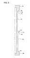
- FIG. 5is a partial sectional view taken along axis 42 of the susceptor illustrated in FIG. 2 .
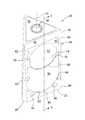
- a barrel susceptor for supporting a plurality of wafers in a barrel reactoris generally indicated by the reference number 20 .
- the susceptor 20includes a polyhedral body 22 having a plurality (e.g., three) trapezoidal faces, generally designated by 24 , positioned symmetrically about an imaginary central axis 26 of the body. Triangular corner pieces 28 may separate the faces 24 of the susceptor 20 .
- the body 22may have other shapes without departing from the scope of the present invention.
- the body 22has a hollow interior (not shown) that is in fluid communication with a port 30 through a top 32 of the body.
- each face 24 of the susceptor 20includes a planar outer surface 40 having an imaginary longitudinal axis 42 extending from a bottom 44 of the face to a top 46 of the face opposite the bottom. Each face 24 slopes inward toward the central axis 26 of the body 22 at the top 46 .
- Each face 24also has a column of shallow recesses 50 , 52 , 54 centered on the corresponding longitudinal axis 42 and two evaluation piece recesses 56 adjacent the bottom 44 of the face.
- the evaluation piece recesses 56may have other dimensions without departing from the scope of the present invention, in one embodiment each evaluation recess has a depth of about 0.050 inch and a diameter of about 1.3 inch. The evaluation recesses are used for holding smaller evaluation wafers, which can be destructively tested to evaluate the epitaxial process without sacrificing a production wafer.
- the bottom recess 50may have other depths without departing from the scope of the present invention, in one embodiment the bottom recess has a depth of about 0.045 inch.
- the bottom recess 50is bordered by a rim, generally designated by 60 , having a narrow rounded lower portion 62 adapted for holding a semiconductor wafer (not shown) during epitaxial processing.
- the rim 60 of the bottom recess 50has narrow straight side portions 64 and a rounded upper portion 66 , all of which are spaced from the wafer during epitaxial processing to allow gas circulation at an upper edge as well as at leading and trailing edges of the wafer in the bottom recess 50 .
- the middle recess 52is positioned above the bottom recess 50 .
- the middle recess 52may have other depths without departing from the scope of the present invention, in one embodiment the middle recess has a depth of about 0.045 inch.
- the middle recess 52has a generally circular rim 70 adapted to hold and surround a semiconductor wafer (not shown) during epitaxial processing.
- the bottom and middle recesses 50 , 52are separated by a curved ledge or protrusion 72 formed between the circular rim 70 of the middle recess and the rounded upper portion 66 of the rim 60 of the bottom recess.
- the ledge 72may have other dimensions without departing from the scope of the present invention, in one embodiment the ledge has a width of about 0.138 inch and is flush with the face 24 of the susceptor 20 . Accordingly, the ledge 72 has an upward facing support surface 74 having a width of about 0.045 inch for supporting a circumferential side of a semiconductor wafer during epitaxial processing.
- the top recess 54surrounds an upper portion of the middle recess 52 .
- the top recess 54may have other depths without departing from the scope of the present invention, in one embodiment the top recess has a depth of about 0.0165 inch.
- the top recess 54is bordered by a rim 80 having narrow straight side portions 82 and a narrow straight upper portion 84 spaced from the wafer during epitaxial processing to allow gas circulation at an upper edge as well as at leading and trailing edges of the wafer.
- each of theses featureshas an arc length of about 120° and a radius approximately equal to that of the wafers intended to be processed using the susceptor 20 (e.g., about 3.97 inches).
- the dimensions of the different recessesmay differ from each other.
- the use and manufacture of the susceptor 20are conventional and well known in the art, they will not be described in further detail.
- a difference between the depth of the middle recess 52 and the depth of the top recess 54generally equals a thickness of the wafer so the outer surface of the wafer is substantially flush with the surface of the top recess.
- Tests using the susceptor 20 described aboveyielded epitaxial thickness profiles that varied by less than about one micrometer over a 200 millimeter (mm) diameter wafer having a three millimeter edge exclusion. Moreover, the actual epitaxial thickness increased near the leading and trailing side edges of the wafer. This compares favorably with tests performed on the conventional susceptor 10 described in the background.
- the conventional susceptoryielded epitaxial thickness profiles that varied by more than about 1.2 micrometers ( ⁇ m) over a 200 millimeter diameter wafer having a three millimeter edge exclusion. Further, the epitaxial thickness decreased by nearly one micrometer near the edges of the wafer compared to the thickness locations spaced from the edge.
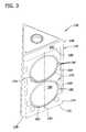
- FIG. 3illustrates a second embodiment of the present invention, in which a barrel susceptor for supporting a plurality of wafers in a barrel reactor is generally indicated by the reference number 120 .
- the susceptor 120is similar to the susceptor 20 of the previous embodiment, like components will be indicated by corresponding reference numerals incremented by 100.
- the susceptor 120includes a polyhedral body 122 having a plurality trapezoidal faces, generally designated by 124 , positioned symmetrically about an imaginary central axis 126 of the body. Triangular corner pieces 128 may separate the faces 124 of the susceptor 120 .
- the body 122may have other shapes without departing from the scope of the present invention.
- Each face 124 of the susceptor 120has a planar outer surface 140 having an imaginary longitudinal axis 142 extending from a bottom 144 of the face to a top 146 of the face opposite the bottom.
- Each face 124also has a shallow recess 150 centered on the corresponding longitudinal axis 142 .
- Each face 124slopes inward toward the central axis 126 of the body 122 at the top 146 .
- each face 124has two evaluation piece recesses 156 adjacent the bottom 144 of the face.
- the recess 150may have other depths without departing from the scope of the present invention, in one embodiment the recess has a depth of about 0.045 inch.
- the recess 150is bordered by a rim, generally designated by 160 , having a narrow rounded lower portion 162 adapted for holding a semiconductor wafer (not shown) during epitaxial processing.
- the rim 160 of the recess 150has narrow straight side portions 164 and a straight upper portion 166 .
- a curved ledge or protrusion 172is provided in the recess 150 for holding a second semiconductor wafer (not shown) during epitaxial processing.
- the ledge 172may have other dimensions without departing from the scope of the present invention, in one embodiment the ledge has a width of about 0.138 inch and is flush with the face 124 of the susceptor 120 .
- the ledge 172has an upward facing support surface 174 having a width of about 0.045 inch for supporting a circumferential side of a semiconductor wafer during epitaxial processing.
- the side portions 164 and upper portion 166 of the rim 160 of the recess 150are spaced from the wafers during epitaxial processing to allow gas circulation at an upper edge as well as at leading and trailing edges of the wafers in the recess.
- the ledge 172 and the rounded lower portion 162 of the rim 160 of the recess 150may have other dimensions without departing from the scope of the present invention, in one embodiment each of these features has an arc length of about 120° and a radius of about 3.97 inches.
- the dimensions of the different recessesmay differ from each other.
- a series of holes 180 arranged in a concentric circular patternis positioned in the recess 150 above the ledge 172 and the rounded lower portion 162 of the rim 160 .
- the holes 190are positioned behind the wafers when positioned in the recess 150 to reduce autodoping.
- the holes 190 and other features of the susceptor 120are conventional, they will not be described further.
- Tests on a susceptor 120 having the configuration described aboveyielded epitaxial thickness profiles that varied by less than about one micrometer over a 200 millimeter (mm) diameter wafer having a three millimeter edge exclusion. As with the susceptor 20 of the first embodiment, the actual epitaxial thickness increased near the leading and trailing side edges of the wafer.
- FIG. 4illustrates a third embodiment of the present invention, in which a barrel susceptor for supporting a plurality of wafers in a barrel reactor is generally indicated by the reference number 220 .
- the susceptor 220is similar to the susceptor 120 of the previous embodiment, like components will be indicated by corresponding reference numerals incremented by 100.
- the susceptor 220includes a polyhedral body 222 having trapezoidal faces 224 positioned symmetrically about an imaginary central axis 226 of the body. Triangular corner pieces 228 separate the faces 224 of the susceptor 220 .
- the body 222may have other shapes without departing from the scope of the present invention.
- Each face 224 of the susceptor 220has a planar outer surface 240 having an imaginary longitudinal axis 242 extending from a bottom 244 of the face to a top 246 of the face opposite the bottom.
- Each face 224also has a shallow rectangular recess 250 centered on the corresponding longitudinal axis 242 and bordered by a rim, generally designated by 260 .
- Each face 224slopes inward toward the central axis 226 of the body 222 at the top 246 .
- the recess 250may have other depths without departing from the scope of the present invention, in one embodiment the recess has a depth of about 0.045 inch.
- a plurality of ledges or protrusions 272is provided in the recess 250 for holding semiconductor wafers (not shown) during epitaxial processing.
- the ledges 272may have other dimensions without departing from the scope of the present invention, in one embodiment each ledge has a width of about 0.125 inch, a length of about 0.250 inch and is flush with the face 224 of the susceptor 220 . Accordingly, each ledge 272 has an upward facing support surface 274 having a width of about 0.045 inch for supporting a circumferential side of a semiconductor wafer during epitaxial processing.
- the ledges 272are positioned at about 50° from the longitudinal axis 242 of the face 224 and at a radius of about 3.94 inches.
- the rim 260 of the recess 250is spaced from the wafers during epitaxial processing to allow gas circulation completely around the wafers in the recess.
- a series of holes 290is positioned in the recess 250 to reduce autodoping.
- Tests on a susceptor 220 having the configuration described aboveyielded epitaxial thickness profiles that varied by less than about one micrometer over a 200 millimeter (mm) diameter wafer having a three millimeter edge exclusion. As with the susceptor 20 of the first embodiment, the actual epitaxial thickness increased near the leading and trailing side edges of the wafer.
Landscapes
- Chemical & Material Sciences (AREA)
- Chemical Kinetics & Catalysis (AREA)
- General Chemical & Material Sciences (AREA)
- Engineering & Computer Science (AREA)
- Materials Engineering (AREA)
- Metallurgy (AREA)
- Organic Chemistry (AREA)
- Crystallography & Structural Chemistry (AREA)
- Mechanical Engineering (AREA)
- Chemical Vapour Deposition (AREA)
- Container, Conveyance, Adherence, Positioning, Of Wafer (AREA)
- Crystals, And After-Treatments Of Crystals (AREA)
Abstract
Description
Claims (7)
Priority Applications (9)
| Application Number | Priority Date | Filing Date | Title |
|---|---|---|---|
| US11/965,521US8404049B2 (en) | 2007-12-27 | 2007-12-27 | Epitaxial barrel susceptor having improved thickness uniformity |
| CN200880122656.3ACN101910475B (en) | 2007-12-27 | 2008-12-22 | Epitaxial cylindrical susceptor with improved thickness uniformity |
| PCT/US2008/087930WO2009086259A1 (en) | 2007-12-27 | 2008-12-22 | Epitaxial barrel susceptor having improved thickness uniformity |
| EP08866204AEP2222901B1 (en) | 2007-12-27 | 2008-12-22 | Epitaxial barrel susceptor producing improved thickness uniformity in an epitaxial coating |
| AT08866204TATE529544T1 (en) | 2007-12-27 | 2008-12-22 | EPITACTIC BARREL SUSCEPTOR FOR IMPROVED UNIFORM THICKNESS OF AN EPITACTIC LAYER |
| MYPI2010002351AMY160289A (en) | 2007-12-27 | 2008-12-22 | Epitaxial barrel susceptor having improved thickness uniformity |
| KR20107014189AKR101478863B1 (en) | 2007-12-27 | 2008-12-22 | Epitaxial barrel susceptor having improved thickness uniformity |
| JP2010540824AJP5237390B2 (en) | 2007-12-27 | 2008-12-22 | Epitaxial barrel susceptor with improved film thickness uniformity |
| TW097151004ATWI416650B (en) | 2007-12-27 | 2008-12-26 | Epitaxial barrel susceptor having improved thickness uniformity |
Applications Claiming Priority (1)
| Application Number | Priority Date | Filing Date | Title |
|---|---|---|---|
| US11/965,521US8404049B2 (en) | 2007-12-27 | 2007-12-27 | Epitaxial barrel susceptor having improved thickness uniformity |
Publications (2)
| Publication Number | Publication Date |
|---|---|
| US20090165719A1 US20090165719A1 (en) | 2009-07-02 |
| US8404049B2true US8404049B2 (en) | 2013-03-26 |
Family
ID=40350145
Family Applications (1)
| Application Number | Title | Priority Date | Filing Date |
|---|---|---|---|
| US11/965,521Active2031-04-30US8404049B2 (en) | 2007-12-27 | 2007-12-27 | Epitaxial barrel susceptor having improved thickness uniformity |
Country Status (9)
| Country | Link |
|---|---|
| US (1) | US8404049B2 (en) |
| EP (1) | EP2222901B1 (en) |
| JP (1) | JP5237390B2 (en) |
| KR (1) | KR101478863B1 (en) |
| CN (1) | CN101910475B (en) |
| AT (1) | ATE529544T1 (en) |
| MY (1) | MY160289A (en) |
| TW (1) | TWI416650B (en) |
| WO (1) | WO2009086259A1 (en) |
Cited By (7)
| Publication number | Priority date | Publication date | Assignee | Title |
|---|---|---|---|---|
| US20110155055A1 (en)* | 2009-12-24 | 2011-06-30 | Hon Hai Precision Industry Co., Ltd. | Cvd device |
| US20110277690A1 (en)* | 2010-05-14 | 2011-11-17 | Sierra Solar Power, Inc. | Multi-channel gas-delivery system |
| US9748434B1 (en) | 2016-05-24 | 2017-08-29 | Tesla, Inc. | Systems, method and apparatus for curing conductive paste |
| US9954136B2 (en) | 2016-08-03 | 2018-04-24 | Tesla, Inc. | Cassette optimized for an inline annealing system |
| US9972740B2 (en) | 2015-06-07 | 2018-05-15 | Tesla, Inc. | Chemical vapor deposition tool and process for fabrication of photovoltaic structures |
| US10115856B2 (en) | 2016-10-31 | 2018-10-30 | Tesla, Inc. | System and method for curing conductive paste using induction heating |
| US10184193B2 (en) | 2015-05-18 | 2019-01-22 | Globalwafers Co., Ltd. | Epitaxy reactor and susceptor system for improved epitaxial wafer flatness |
Families Citing this family (4)
| Publication number | Priority date | Publication date | Assignee | Title |
|---|---|---|---|---|
| CN205845916U (en)* | 2013-07-09 | 2016-12-28 | 应用材料公司 | Equipment for handling substrates |
| CN106575636A (en)* | 2014-08-22 | 2017-04-19 | 应用材料公司 | High-speed epitaxy systems and methods |
| CN106906455A (en)* | 2017-03-30 | 2017-06-30 | 河北普兴电子科技股份有限公司 | The trapezoidal pedestal of silicon epitaxial reaction cavity |
| CN110494215A (en) | 2017-04-11 | 2019-11-22 | 株式会社科特拉 | Exhaust gas purification catalyst |
Citations (62)
| Publication number | Priority date | Publication date | Assignee | Title |
|---|---|---|---|---|
| US3675619A (en) | 1969-02-25 | 1972-07-11 | Monsanto Co | Apparatus for production of epitaxial films |
| US3806360A (en) | 1966-12-15 | 1974-04-23 | Western Electric Co | Methods for heating and/or coating articles |
| US4322592A (en)* | 1980-08-22 | 1982-03-30 | Rca Corporation | Susceptor for heating semiconductor substrates |
| JPS58217495A (en) | 1982-06-11 | 1983-12-17 | Toshiba Corp | Heating base for vapor phase growth furnace |
| US4496609A (en) | 1969-10-15 | 1985-01-29 | Applied Materials, Inc. | Chemical vapor deposition coating process employing radiant heat and a susceptor |
| US4728389A (en) | 1985-05-20 | 1988-03-01 | Applied Materials, Inc. | Particulate-free epitaxial process |
| EP0289560A1 (en) | 1986-11-10 | 1988-11-09 | Ncr Co | Terminator for a transceiver device. |
| US4823736A (en) | 1985-07-22 | 1989-04-25 | Air Products And Chemicals, Inc. | Barrel structure for semiconductor epitaxial reactor |
| US5192371A (en) | 1991-05-21 | 1993-03-09 | Asm Japan K.K. | Substrate supporting apparatus for a CVD apparatus |
| US5200157A (en) | 1986-02-17 | 1993-04-06 | Toshiba Ceramics Co., Ltd. | Susceptor for vapor-growth deposition |
| US5242501A (en) | 1982-09-10 | 1993-09-07 | Lam Research Corporation | Susceptor in chemical vapor deposition reactors |
| US5288364A (en) | 1992-08-20 | 1994-02-22 | Motorola, Inc. | Silicon epitaxial reactor and control method |
| US5298107A (en) | 1992-02-27 | 1994-03-29 | Applied Materials, Inc. | Processing method for growing thick films |
| WO1994017353A1 (en) | 1993-01-21 | 1994-08-04 | Moore Epitaxial, Inc. | A rapid thermal processing apparatus for processing semiconductor wafers |
| US5350455A (en) | 1993-02-25 | 1994-09-27 | Leybold Aktiengesellschaft | Device for holding disk-shaped substrates in the vacuum chamber of a coating or etching apparatus |
| JPH06310431A (en) | 1993-04-27 | 1994-11-04 | Fuji Electric Co Ltd | Barrel type vapor phase growth equipment |
| US5373806A (en) | 1985-05-20 | 1994-12-20 | Applied Materials, Inc. | Particulate-free epitaxial process |
| US5374159A (en) | 1989-05-19 | 1994-12-20 | Applied Materials, Inc. | Robotically loaded epitaxial deposition apparatus |
| JPH0774114A (en)* | 1993-09-03 | 1995-03-17 | Komatsu Electron Metals Co Ltd | Barrel type susceptor for vapor phase epitaxy |
| US5439523A (en) | 1994-02-14 | 1995-08-08 | Memc Electronic Materials, Inc. | Device for suppressing particle splash onto a semiconductor wafer |
| US5441571A (en) | 1992-09-28 | 1995-08-15 | Shin-Etsu Handotai Co., Ltd. | Cylindrical apparatus for growth of epitaxial layers |
| WO1996010659A2 (en) | 1994-09-30 | 1996-04-11 | Lpe Spa | An epitaxial reactor, susceptor and gas-flow system |
| US5516367A (en) | 1993-04-05 | 1996-05-14 | Applied Materials, Inc. | Chemical vapor deposition chamber with a purge guide |
| US5518549A (en) | 1995-04-18 | 1996-05-21 | Memc Electronic Materials, Inc. | Susceptor and baffle therefor |
| US5527393A (en) | 1990-03-19 | 1996-06-18 | Kabushiki Kaisha Toshiba | Vapor-phase deposition apparatus and vapor-phase deposition method |
| US5580388A (en) | 1993-01-21 | 1996-12-03 | Moore Epitaxial, Inc. | Multi-layer susceptor for rapid thermal process reactors |
| EP0757117A1 (en) | 1995-08-01 | 1997-02-05 | MEMC Electronic Materials, Inc. | Method and apparatus for deposition of material on a semiconductor wafer |
| WO1997008743A1 (en) | 1995-08-22 | 1997-03-06 | Advanced Semiconductor Materials America, Inc. | Low mass susceptor |
| US5679405A (en) | 1990-07-16 | 1997-10-21 | National Semiconductor Corp. | Method for preventing substrate backside deposition during a chemical vapor deposition operation |
| US5769942A (en) | 1994-09-29 | 1998-06-23 | Semiconductor Process Laboratory Co. | Method for epitaxial growth |
| US5785764A (en) | 1996-09-10 | 1998-07-28 | Shin-Etsu Handotai Co., Ltd. | Susceptor for a gas phase growth apparatus |
| EP0863541A1 (en) | 1994-02-12 | 1998-09-09 | Shin-Etsu Handotai Company Limited | Method for the production of a semiconductor single crystalline substrate having a chamfer and a protecting film |
| US5820686A (en) | 1993-01-21 | 1998-10-13 | Moore Epitaxial, Inc. | Multi-layer susceptor for rapid thermal process reactors |
| US5897380A (en) | 1994-11-09 | 1999-04-27 | Tokyo Electron Limited | Method for isolating a susceptor heating element from a chemical vapor deposition environment |
| WO1999023691A2 (en) | 1997-11-03 | 1999-05-14 | Asm America, Inc. | Improved low mass wafer support system |
| US5904769A (en) | 1996-01-12 | 1999-05-18 | Toshiba Ceramics Co., Ltd. | Epitaxial growth method |
| US5960555A (en) | 1996-07-24 | 1999-10-05 | Applied Materials, Inc. | Method and apparatus for purging the back side of a substrate during chemical vapor processing |
| US5968277A (en) | 1997-10-10 | 1999-10-19 | Seh America, Inc. | Susceptor apparatus for epitaxial deposition and method for reducing slip formation on semiconductor substrates |
| WO2000000664A1 (en) | 1998-06-30 | 2000-01-06 | Memc Electronic Materials, Inc. | Susceptor for barrel reactor |
| JP2000133187A (en) | 1998-10-22 | 2000-05-12 | Hitachi Ltd | Sample stage of electron microscope |
| US6110289A (en)* | 1997-02-25 | 2000-08-29 | Moore Epitaxial, Inc. | Rapid thermal processing barrel reactor for processing substrates |
| WO2000058533A1 (en) | 1999-03-25 | 2000-10-05 | Lpe Spa | Reaction chamber for an epitaxial reactor |
| US6129047A (en) | 1997-02-07 | 2000-10-10 | Sumitomo Metal Industries, Ltd. | Susceptor for vapor-phase growth apparatus |
| US6184154B1 (en) | 1999-10-13 | 2001-02-06 | Seh America, Inc. | Method of processing the backside of a wafer within an epitaxial reactor chamber |
| US20020088389A1 (en) | 2000-11-17 | 2002-07-11 | Memc Electronic Materials, Inc. | High throughput epitaxial growth by chemical vapor deposition |
| US6444027B1 (en) | 2000-05-08 | 2002-09-03 | Memc Electronic Materials, Inc. | Modified susceptor for use in chemical vapor deposition process |
| EP1308989A2 (en) | 1997-11-03 | 2003-05-07 | ASM America, Inc. | Improved low mass wafer support system |
| US20040266181A1 (en) | 2003-06-26 | 2004-12-30 | Siltronic Ag | Coated semiconductor wafer, and process and device for producing the semiconductor wafer |
| US20050160991A1 (en) | 2003-12-22 | 2005-07-28 | Toshiba Ceramics Co., Ltd. | Barrel type susceptor |
| US20060079089A1 (en) | 2003-06-26 | 2006-04-13 | Siltronic Ag | Coated semiconductor wafer, and process and apparatus for producing the semiconductor wafer |
| US7048316B1 (en) | 2002-07-12 | 2006-05-23 | Novellus Systems, Inc. | Compound angled pad end-effector |
| US7081165B2 (en) | 2001-05-18 | 2006-07-25 | Lg.Philips Lcd Co., Ltd. | Chemical vapor deposition apparatus having a susceptor with a grounded lift pin |
| US20060201623A1 (en) | 2005-03-09 | 2006-09-14 | Yoo Woo S | Low temperature wafer backside cleaning |
| US7122844B2 (en) | 2002-05-13 | 2006-10-17 | Cree, Inc. | Susceptor for MOCVD reactor |
| US20060231035A1 (en) | 2005-04-15 | 2006-10-19 | Memc Electronic Materials, Inc. | Modified susceptor for barrel reactor |
| EP1732111A1 (en) | 2004-03-31 | 2006-12-13 | Toyo Tanso Co., Ltd. | Susceptor |
| US20060291835A1 (en) | 2005-06-23 | 2006-12-28 | Dainippon Screen Mfg., Co., Ltd. | Susceptor for heat treatment and heat treatment apparatus |
| US20070218702A1 (en) | 2006-03-15 | 2007-09-20 | Asm Japan K.K. | Semiconductor-processing apparatus with rotating susceptor |
| US7276123B2 (en) | 2003-07-28 | 2007-10-02 | Asm Japan K.K. | Semiconductor-processing apparatus provided with susceptor and placing block |
| US20080110401A1 (en) | 2004-05-18 | 2008-05-15 | Sumco Corporation | Susceptor For Vapor-Phase Growth Reactor |
| US7393417B1 (en) | 1999-10-29 | 2008-07-01 | Applied Materials, Inc. | Semiconductor-manufacturing apparatus |
| US20080206464A1 (en) | 2004-12-04 | 2008-08-28 | Aixtron Inc. | Method and Device for the Depositing of Gallium Nitrite Layers on a Sapphire Substrate and Associated Substrate Holder |
Family Cites Families (2)
| Publication number | Priority date | Publication date | Assignee | Title |
|---|---|---|---|---|
| JPS61171242U (en)* | 1985-04-11 | 1986-10-24 | ||
| JPH07120628B2 (en)* | 1988-04-08 | 1995-12-20 | 三菱化学株式会社 | Barrel type susceptor |
- 2007
- 2007-12-27USUS11/965,521patent/US8404049B2/enactiveActive
- 2008
- 2008-12-22WOPCT/US2008/087930patent/WO2009086259A1/enactiveApplication Filing
- 2008-12-22MYMYPI2010002351Apatent/MY160289A/enunknown
- 2008-12-22KRKR20107014189Apatent/KR101478863B1/enactiveActive
- 2008-12-22EPEP08866204Apatent/EP2222901B1/enactiveActive
- 2008-12-22ATAT08866204Tpatent/ATE529544T1/ennot_activeIP Right Cessation
- 2008-12-22JPJP2010540824Apatent/JP5237390B2/enactiveActive
- 2008-12-22CNCN200880122656.3Apatent/CN101910475B/enactiveActive
- 2008-12-26TWTW097151004Apatent/TWI416650B/enactive
Patent Citations (86)
| Publication number | Priority date | Publication date | Assignee | Title |
|---|---|---|---|---|
| US3806360A (en) | 1966-12-15 | 1974-04-23 | Western Electric Co | Methods for heating and/or coating articles |
| US3675619A (en) | 1969-02-25 | 1972-07-11 | Monsanto Co | Apparatus for production of epitaxial films |
| US4496609A (en) | 1969-10-15 | 1985-01-29 | Applied Materials, Inc. | Chemical vapor deposition coating process employing radiant heat and a susceptor |
| US4322592A (en)* | 1980-08-22 | 1982-03-30 | Rca Corporation | Susceptor for heating semiconductor substrates |
| JPS58217495A (en) | 1982-06-11 | 1983-12-17 | Toshiba Corp | Heating base for vapor phase growth furnace |
| US5242501A (en) | 1982-09-10 | 1993-09-07 | Lam Research Corporation | Susceptor in chemical vapor deposition reactors |
| US4728389A (en) | 1985-05-20 | 1988-03-01 | Applied Materials, Inc. | Particulate-free epitaxial process |
| US5373806A (en) | 1985-05-20 | 1994-12-20 | Applied Materials, Inc. | Particulate-free epitaxial process |
| US4823736A (en) | 1985-07-22 | 1989-04-25 | Air Products And Chemicals, Inc. | Barrel structure for semiconductor epitaxial reactor |
| US5200157A (en) | 1986-02-17 | 1993-04-06 | Toshiba Ceramics Co., Ltd. | Susceptor for vapor-growth deposition |
| EP0289560A1 (en) | 1986-11-10 | 1988-11-09 | Ncr Co | Terminator for a transceiver device. |
| US5374159A (en) | 1989-05-19 | 1994-12-20 | Applied Materials, Inc. | Robotically loaded epitaxial deposition apparatus |
| US5476359A (en) | 1989-05-19 | 1995-12-19 | Applied Materials, Inc. | Robotically loaded epitaxial deposition apparatus |
| US5527393A (en) | 1990-03-19 | 1996-06-18 | Kabushiki Kaisha Toshiba | Vapor-phase deposition apparatus and vapor-phase deposition method |
| US5679405A (en) | 1990-07-16 | 1997-10-21 | National Semiconductor Corp. | Method for preventing substrate backside deposition during a chemical vapor deposition operation |
| US5192371A (en) | 1991-05-21 | 1993-03-09 | Asm Japan K.K. | Substrate supporting apparatus for a CVD apparatus |
| US5298107A (en) | 1992-02-27 | 1994-03-29 | Applied Materials, Inc. | Processing method for growing thick films |
| US5288364A (en) | 1992-08-20 | 1994-02-22 | Motorola, Inc. | Silicon epitaxial reactor and control method |
| US5441571A (en) | 1992-09-28 | 1995-08-15 | Shin-Etsu Handotai Co., Ltd. | Cylindrical apparatus for growth of epitaxial layers |
| EP1154039A1 (en) | 1993-01-21 | 2001-11-14 | Moore Epitaxial, Inc. | A rapid thermal processing apparatus for processing semiconductor wafers |
| EP0633997B1 (en) | 1993-01-21 | 2001-11-28 | Moore Epitaxial, Inc. | A rapid thermal processing apparatus for processing semiconductor wafers |
| WO1994017353A1 (en) | 1993-01-21 | 1994-08-04 | Moore Epitaxial, Inc. | A rapid thermal processing apparatus for processing semiconductor wafers |
| EP1154039B1 (en) | 1993-01-21 | 2006-06-21 | Moore Epitaxial, Inc. | A rapid thermal processing apparatus for processing semiconductor wafers |
| US5820686A (en) | 1993-01-21 | 1998-10-13 | Moore Epitaxial, Inc. | Multi-layer susceptor for rapid thermal process reactors |
| US5580388A (en) | 1993-01-21 | 1996-12-03 | Moore Epitaxial, Inc. | Multi-layer susceptor for rapid thermal process reactors |
| US5350455A (en) | 1993-02-25 | 1994-09-27 | Leybold Aktiengesellschaft | Device for holding disk-shaped substrates in the vacuum chamber of a coating or etching apparatus |
| US5516367A (en) | 1993-04-05 | 1996-05-14 | Applied Materials, Inc. | Chemical vapor deposition chamber with a purge guide |
| JPH06310431A (en) | 1993-04-27 | 1994-11-04 | Fuji Electric Co Ltd | Barrel type vapor phase growth equipment |
| JPH0774114A (en)* | 1993-09-03 | 1995-03-17 | Komatsu Electron Metals Co Ltd | Barrel type susceptor for vapor phase epitaxy |
| EP0863541A1 (en) | 1994-02-12 | 1998-09-09 | Shin-Etsu Handotai Company Limited | Method for the production of a semiconductor single crystalline substrate having a chamfer and a protecting film |
| US5439523A (en) | 1994-02-14 | 1995-08-08 | Memc Electronic Materials, Inc. | Device for suppressing particle splash onto a semiconductor wafer |
| US5769942A (en) | 1994-09-29 | 1998-06-23 | Semiconductor Process Laboratory Co. | Method for epitaxial growth |
| EP0730679B1 (en) | 1994-09-30 | 2001-12-12 | Lpe Spa | An epitaxial reactor, susceptor and gas-flow system |
| WO1996010659A2 (en) | 1994-09-30 | 1996-04-11 | Lpe Spa | An epitaxial reactor, susceptor and gas-flow system |
| US5897380A (en) | 1994-11-09 | 1999-04-27 | Tokyo Electron Limited | Method for isolating a susceptor heating element from a chemical vapor deposition environment |
| EP0738789A2 (en) | 1995-04-18 | 1996-10-23 | MEMC Electronic Materials, Inc. | Susceptor and baffle therefor |
| US5518549A (en) | 1995-04-18 | 1996-05-21 | Memc Electronic Materials, Inc. | Susceptor and baffle therefor |
| JPH08325093A (en) | 1995-04-18 | 1996-12-10 | Memc Electron Materials Inc | Suscepter |
| EP0746009B1 (en) | 1995-05-30 | 2003-01-02 | Moore Epitaxial, Inc. | Multi-layer susceptor for rapid thermal process reactors |
| EP0746009A1 (en) | 1995-05-30 | 1996-12-04 | Moore Epitaxial, Inc. | Multi-layer susceptor for rapid thermal process reactors |
| EP0757117A1 (en) | 1995-08-01 | 1997-02-05 | MEMC Electronic Materials, Inc. | Method and apparatus for deposition of material on a semiconductor wafer |
| EP0757117B1 (en) | 1995-08-01 | 1999-07-07 | MEMC Electronic Materials, Inc. | Method and apparatus for deposition of material on a semiconductor wafer |
| WO1997008743A1 (en) | 1995-08-22 | 1997-03-06 | Advanced Semiconductor Materials America, Inc. | Low mass susceptor |
| US6086680A (en) | 1995-08-22 | 2000-07-11 | Asm America, Inc. | Low-mass susceptor |
| US5904769A (en) | 1996-01-12 | 1999-05-18 | Toshiba Ceramics Co., Ltd. | Epitaxial growth method |
| US5960555A (en) | 1996-07-24 | 1999-10-05 | Applied Materials, Inc. | Method and apparatus for purging the back side of a substrate during chemical vapor processing |
| US5785764A (en) | 1996-09-10 | 1998-07-28 | Shin-Etsu Handotai Co., Ltd. | Susceptor for a gas phase growth apparatus |
| TW391999B (en) | 1996-09-10 | 2000-06-01 | Shinetsu Handotai Kk | A susceptor for a gas phase growth apparatus |
| US6129047A (en) | 1997-02-07 | 2000-10-10 | Sumitomo Metal Industries, Ltd. | Susceptor for vapor-phase growth apparatus |
| US6110289A (en)* | 1997-02-25 | 2000-08-29 | Moore Epitaxial, Inc. | Rapid thermal processing barrel reactor for processing substrates |
| US5968277A (en) | 1997-10-10 | 1999-10-19 | Seh America, Inc. | Susceptor apparatus for epitaxial deposition and method for reducing slip formation on semiconductor substrates |
| US6454865B1 (en) | 1997-11-03 | 2002-09-24 | Asm America, Inc. | Low mass wafer support system |
| WO1999023691A2 (en) | 1997-11-03 | 1999-05-14 | Asm America, Inc. | Improved low mass wafer support system |
| US20050183829A1 (en) | 1997-11-03 | 2005-08-25 | Goodman Matthew G. | Low-mass susceptor improvements |
| EP1308989A2 (en) | 1997-11-03 | 2003-05-07 | ASM America, Inc. | Improved low mass wafer support system |
| US20020043337A1 (en) | 1997-11-03 | 2002-04-18 | Goodman Matthew G. | Low mass wafer support system |
| WO2000000664A1 (en) | 1998-06-30 | 2000-01-06 | Memc Electronic Materials, Inc. | Susceptor for barrel reactor |
| US6129048A (en)* | 1998-06-30 | 2000-10-10 | Memc Electronic Materials, Inc. | Susceptor for barrel reactor |
| JP2000133187A (en) | 1998-10-22 | 2000-05-12 | Hitachi Ltd | Sample stage of electron microscope |
| EP1173632B1 (en) | 1999-03-25 | 2003-10-22 | Lpe Spa | Reaction chamber for an epitaxial reactor |
| WO2000058533A1 (en) | 1999-03-25 | 2000-10-05 | Lpe Spa | Reaction chamber for an epitaxial reactor |
| US6184154B1 (en) | 1999-10-13 | 2001-02-06 | Seh America, Inc. | Method of processing the backside of a wafer within an epitaxial reactor chamber |
| US7393417B1 (en) | 1999-10-29 | 2008-07-01 | Applied Materials, Inc. | Semiconductor-manufacturing apparatus |
| US6596095B2 (en) | 2000-05-08 | 2003-07-22 | Memc Electronic Materials, Inc. | Epitaxial silicon wafer free from autodoping and backside halo and a method and apparatus for the preparation thereof |
| US6652650B2 (en) | 2000-05-08 | 2003-11-25 | Memc Electronic Materials, Inc. | Modified susceptor for use in chemical vapor deposition process |
| US6444027B1 (en) | 2000-05-08 | 2002-09-03 | Memc Electronic Materials, Inc. | Modified susceptor for use in chemical vapor deposition process |
| US20020088389A1 (en) | 2000-11-17 | 2002-07-11 | Memc Electronic Materials, Inc. | High throughput epitaxial growth by chemical vapor deposition |
| US20030037723A9 (en) | 2000-11-17 | 2003-02-27 | Memc Electronic Materials, Inc. | High throughput epitaxial growth by chemical vapor deposition |
| US7081165B2 (en) | 2001-05-18 | 2006-07-25 | Lg.Philips Lcd Co., Ltd. | Chemical vapor deposition apparatus having a susceptor with a grounded lift pin |
| US7122844B2 (en) | 2002-05-13 | 2006-10-17 | Cree, Inc. | Susceptor for MOCVD reactor |
| US7048316B1 (en) | 2002-07-12 | 2006-05-23 | Novellus Systems, Inc. | Compound angled pad end-effector |
| US7285483B2 (en) | 2003-06-26 | 2007-10-23 | Silitronic Ag | Coated semiconductor wafer, and process and apparatus for producing the semiconductor wafer |
| US20060079089A1 (en) | 2003-06-26 | 2006-04-13 | Siltronic Ag | Coated semiconductor wafer, and process and apparatus for producing the semiconductor wafer |
| US7101794B2 (en) | 2003-06-26 | 2006-09-05 | Siltronic Ag | Coated semiconductor wafer, and process and device for producing the semiconductor wafer |
| US20040266181A1 (en) | 2003-06-26 | 2004-12-30 | Siltronic Ag | Coated semiconductor wafer, and process and device for producing the semiconductor wafer |
| US7276123B2 (en) | 2003-07-28 | 2007-10-02 | Asm Japan K.K. | Semiconductor-processing apparatus provided with susceptor and placing block |
| US20050160991A1 (en) | 2003-12-22 | 2005-07-28 | Toshiba Ceramics Co., Ltd. | Barrel type susceptor |
| US7276125B2 (en) | 2003-12-22 | 2007-10-02 | Toshiba Ceramics Co., Ltd. | Barrel type susceptor |
| US20070186858A1 (en) | 2004-03-31 | 2007-08-16 | Toyo Tanso Co., Ltd. | Susceptor |
| EP1732111A1 (en) | 2004-03-31 | 2006-12-13 | Toyo Tanso Co., Ltd. | Susceptor |
| US20080110401A1 (en) | 2004-05-18 | 2008-05-15 | Sumco Corporation | Susceptor For Vapor-Phase Growth Reactor |
| US20080206464A1 (en) | 2004-12-04 | 2008-08-28 | Aixtron Inc. | Method and Device for the Depositing of Gallium Nitrite Layers on a Sapphire Substrate and Associated Substrate Holder |
| US20060201623A1 (en) | 2005-03-09 | 2006-09-14 | Yoo Woo S | Low temperature wafer backside cleaning |
| US20060231035A1 (en) | 2005-04-15 | 2006-10-19 | Memc Electronic Materials, Inc. | Modified susceptor for barrel reactor |
| US20060291835A1 (en) | 2005-06-23 | 2006-12-28 | Dainippon Screen Mfg., Co., Ltd. | Susceptor for heat treatment and heat treatment apparatus |
| US20070218702A1 (en) | 2006-03-15 | 2007-09-20 | Asm Japan K.K. | Semiconductor-processing apparatus with rotating susceptor |
Non-Patent Citations (4)
| Title |
|---|
| Chinese Office Action dated Nov. 11, 2011 regarding Application No. 200880122656.3 filed on Jun. 24, 2010, 13 pages. |
| International Search Report and Written Opinion from related application No. PCT/US2008/087930, dated Mar. 3, 2009. |
| Japanese Office Action dated Jan. 24, 2012 regarding Application No. 2010-540824; 6 pages. |
| Singapore Written Opinion from Singapore Patent Application No. 201003884-2 filed on Dec. 22, 2008, dated Jun. 8, 2011; 5 pages. |
Cited By (10)
| Publication number | Priority date | Publication date | Assignee | Title |
|---|---|---|---|---|
| US20110155055A1 (en)* | 2009-12-24 | 2011-06-30 | Hon Hai Precision Industry Co., Ltd. | Cvd device |
| US8608854B2 (en)* | 2009-12-24 | 2013-12-17 | Hon Hai Precision Industry Co., Ltd. | CVD device |
| US20110277690A1 (en)* | 2010-05-14 | 2011-11-17 | Sierra Solar Power, Inc. | Multi-channel gas-delivery system |
| US9441295B2 (en)* | 2010-05-14 | 2016-09-13 | Solarcity Corporation | Multi-channel gas-delivery system |
| US10184193B2 (en) | 2015-05-18 | 2019-01-22 | Globalwafers Co., Ltd. | Epitaxy reactor and susceptor system for improved epitaxial wafer flatness |
| US9972740B2 (en) | 2015-06-07 | 2018-05-15 | Tesla, Inc. | Chemical vapor deposition tool and process for fabrication of photovoltaic structures |
| US9748434B1 (en) | 2016-05-24 | 2017-08-29 | Tesla, Inc. | Systems, method and apparatus for curing conductive paste |
| US10074765B2 (en) | 2016-05-24 | 2018-09-11 | Tesla, Inc. | Systems, method and apparatus for curing conductive paste |
| US9954136B2 (en) | 2016-08-03 | 2018-04-24 | Tesla, Inc. | Cassette optimized for an inline annealing system |
| US10115856B2 (en) | 2016-10-31 | 2018-10-30 | Tesla, Inc. | System and method for curing conductive paste using induction heating |
Also Published As
| Publication number | Publication date |
|---|---|
| EP2222901B1 (en) | 2011-10-19 |
| JP2011508455A (en) | 2011-03-10 |
| TW200939384A (en) | 2009-09-16 |
| CN101910475A (en) | 2010-12-08 |
| MY160289A (en) | 2017-02-28 |
| JP5237390B2 (en) | 2013-07-17 |
| KR101478863B1 (en) | 2015-01-02 |
| US20090165719A1 (en) | 2009-07-02 |
| EP2222901A1 (en) | 2010-09-01 |
| KR20100113067A (en) | 2010-10-20 |
| ATE529544T1 (en) | 2011-11-15 |
| WO2009086259A1 (en) | 2009-07-09 |
| CN101910475B (en) | 2013-06-12 |
| TWI416650B (en) | 2013-11-21 |
Similar Documents
| Publication | Publication Date | Title |
|---|---|---|
| US8404049B2 (en) | Epitaxial barrel susceptor having improved thickness uniformity | |
| US11885019B2 (en) | Susceptor with ring to limit backside deposition | |
| KR102417931B1 (en) | Substrate supporting device and substrate processing apparatus including the same | |
| EP2165358B1 (en) | Susceptor for improving throughput and reducing wafer damage | |
| JP5158093B2 (en) | Vapor growth susceptor and vapor growth apparatus | |
| KR101608947B1 (en) | Semiconductor substrate support susceptor for vapor-phase epitaxy, epitaxial wafer manufacturing device, and epitaxial wafer manufacturing method | |
| US20100107974A1 (en) | Substrate holder with varying density | |
| US8088225B2 (en) | Substrate support system for reduced autodoping and backside deposition | |
| US20090165721A1 (en) | Susceptor with Support Bosses | |
| US8940094B2 (en) | Methods for fabricating a semiconductor wafer processing device | |
| US10184193B2 (en) | Epitaxy reactor and susceptor system for improved epitaxial wafer flatness | |
| TWI628734B (en) | Susceptor for improved epitaxial wafer flatness and methods for fabricating a semiconductor wafer processing device | |
| CN108630594B (en) | Substrate processing apparatus | |
| US12351940B2 (en) | Liner and epitaxial reactor comprising same | |
| US20150284847A1 (en) | Method of Forming an Epitaxial Layer and Apparatus for Processing a Substrate Used for the Method | |
| US20130263779A1 (en) | Susceptor For Improved Epitaxial Wafer Flatness | |
| KR101259006B1 (en) | Susceptor device for manufacturing semiconductor | |
| KR20120079315A (en) | Susceptor for chemical vapor deposition apparatus | |
| KR20130080645A (en) | Susceptor for manufacturing semiconductor | |
| KR20120108092A (en) | Barrel susceptor | |
| KR20130083319A (en) | Susceptor |
Legal Events
| Date | Code | Title | Description |
|---|---|---|---|
| AS | Assignment | Owner name:MEMC ELECTRONIC MATERIALS, INC., MISSOURI Free format text:ASSIGNMENT OF ASSIGNORS INTEREST;ASSIGNORS:HELLWIG, LANCE G.;KOMMU, SRIKANTH;PITNEY, JOHN A.;REEL/FRAME:020483/0271;SIGNING DATES FROM 20080116 TO 20080205 Owner name:MEMC ELECTRONIC MATERIALS, INC., MISSOURI Free format text:ASSIGNMENT OF ASSIGNORS INTEREST;ASSIGNORS:HELLWIG, LANCE G.;KOMMU, SRIKANTH;PITNEY, JOHN A.;SIGNING DATES FROM 20080116 TO 20080205;REEL/FRAME:020483/0271 | |
| AS | Assignment | Owner name:BANK OF AMERICA, N.A., MASSACHUSETTS Free format text:SECURITY AGREEMENT;ASSIGNORS:MEMC ELECTRONIC MATERIALS, INC.;SUNEDISON LLC;SOLAICX;REEL/FRAME:026064/0720 Effective date:20110317 | |
| AS | Assignment | Owner name:GOLDMAN SACHS BANK USA, NEW JERSEY Free format text:SECURITY AGREEMENT;ASSIGNORS:NVT, LLC;SUN EDISON LLC;SOLAICX, INC.;AND OTHERS;REEL/FRAME:029057/0810 Effective date:20120928 | |
| STCF | Information on status: patent grant | Free format text:PATENTED CASE | |
| AS | Assignment | Owner name:SOLAICX, OREGON Free format text:RELEASE BY SECURED PARTY;ASSIGNOR:BANK OF AMERICA, N.A.;REEL/FRAME:031870/0031 Effective date:20131220 Owner name:SUN EDISON LLC, CALIFORNIA Free format text:RELEASE BY SECURED PARTY;ASSIGNOR:GOLDMAN SACHS BANK USA;REEL/FRAME:031870/0092 Effective date:20131220 Owner name:NVT, LLC, CALIFORNIA Free format text:RELEASE BY SECURED PARTY;ASSIGNOR:GOLDMAN SACHS BANK USA;REEL/FRAME:031870/0092 Effective date:20131220 Owner name:ENFLEX CORPORATION, CALIFORNIA Free format text:RELEASE BY SECURED PARTY;ASSIGNOR:BANK OF AMERICA, N.A.;REEL/FRAME:031870/0031 Effective date:20131220 Owner name:SUN EDISON LLC, CALIFORNIA Free format text:RELEASE BY SECURED PARTY;ASSIGNOR:BANK OF AMERICA, N.A.;REEL/FRAME:031870/0031 Effective date:20131220 Owner name:SUNEDISON, INC. (F/K/A MEMC ELECTRONIC MATERIALS, Free format text:RELEASE BY SECURED PARTY;ASSIGNOR:GOLDMAN SACHS BANK USA;REEL/FRAME:031870/0092 Effective date:20131220 Owner name:SOLAICX, OREGON Free format text:RELEASE BY SECURED PARTY;ASSIGNOR:GOLDMAN SACHS BANK USA;REEL/FRAME:031870/0092 Effective date:20131220 Owner name:SUNEDISON, INC. (F/K/A MEMC ELECTRONIC MATERIALS, Free format text:RELEASE BY SECURED PARTY;ASSIGNOR:BANK OF AMERICA, N.A.;REEL/FRAME:031870/0031 Effective date:20131220 | |
| AS | Assignment | Owner name:DEUTSCHE BANK AG NEW YORK BRANCH, NEW JERSEY Free format text:SECURITY AGREEMENT;ASSIGNORS:SUNEDISON, INC.;SOLAICX;SUN EDISON, LLC;AND OTHERS;REEL/FRAME:032177/0359 Effective date:20140115 | |
| AS | Assignment | Owner name:SOLAICX, OREGON Free format text:RELEASE BY SECURED PARTY;ASSIGNOR:DEUTSCHE BANK AG NEW YORK BRANCH;REEL/FRAME:032382/0724 Effective date:20140228 Owner name:NVT, LLC, MARYLAND Free format text:RELEASE BY SECURED PARTY;ASSIGNOR:DEUTSCHE BANK AG NEW YORK BRANCH;REEL/FRAME:032382/0724 Effective date:20140228 Owner name:SUN EDISON LLC, CALIFORNIA Free format text:RELEASE BY SECURED PARTY;ASSIGNOR:DEUTSCHE BANK AG NEW YORK BRANCH;REEL/FRAME:032382/0724 Effective date:20140228 Owner name:SUNEDISON, INC., MISSOURI Free format text:RELEASE BY SECURED PARTY;ASSIGNOR:DEUTSCHE BANK AG NEW YORK BRANCH;REEL/FRAME:032382/0724 Effective date:20140228 | |
| AS | Assignment | Owner name:SUNEDISON SEMICONDUCTOR LIMITED (UEN201334164H), S Free format text:ASSIGNMENT OF ASSIGNORS INTEREST;ASSIGNOR:MEMC ELECTRONIC MATERIALS, INC.;REEL/FRAME:033023/0430 Effective date:20140523 | |
| AS | Assignment | Owner name:SUNEDISON SEMICONDUCTOR TECHNOLOGY PTE. LTD., MISS Free format text:NOTICE OF LICENSE AGREEMENT;ASSIGNOR:SUNEDISON SEMICONDUCTOR LIMITED;REEL/FRAME:033099/0001 Effective date:20140527 | |
| CC | Certificate of correction | ||
| FPAY | Fee payment | Year of fee payment:4 | |
| AS | Assignment | Owner name:GLOBALWAFERS CO., LTD., TAIWAN Free format text:ASSIGNMENT OF ASSIGNORS INTEREST;ASSIGNORS:SUNEDISON SEMICONDUCTOR LIMITED;MEMC JAPAN LIMITED;MEMC ELECTRONIC MATERIALS S.P.A.;REEL/FRAME:046327/0001 Effective date:20180606 | |
| MAFP | Maintenance fee payment | Free format text:PAYMENT OF MAINTENANCE FEE, 8TH YEAR, LARGE ENTITY (ORIGINAL EVENT CODE: M1552); ENTITY STATUS OF PATENT OWNER: LARGE ENTITY Year of fee payment:8 | |
| MAFP | Maintenance fee payment | Free format text:PAYMENT OF MAINTENANCE FEE, 12TH YEAR, LARGE ENTITY (ORIGINAL EVENT CODE: M1553); ENTITY STATUS OF PATENT OWNER: LARGE ENTITY Year of fee payment:12 |