US8402918B2 - Showerhead electrode with centering feature - Google Patents
Showerhead electrode with centering featureDownload PDFInfo
- Publication number
- US8402918B2 US8402918B2US12/419,878US41987809AUS8402918B2US 8402918 B2US8402918 B2US 8402918B2US 41987809 AUS41987809 AUS 41987809AUS 8402918 B2US8402918 B2US 8402918B2
- Authority
- US
- United States
- Prior art keywords
- electrode
- wall
- centering ring
- backing plate
- showerhead electrode
- Prior art date
- Legal status (The legal status is an assumption and is not a legal conclusion. Google has not performed a legal analysis and makes no representation as to the accuracy of the status listed.)
- Active, expires
Links
Images


Classifications
- H—ELECTRICITY
- H01—ELECTRIC ELEMENTS
- H01J—ELECTRIC DISCHARGE TUBES OR DISCHARGE LAMPS
- H01J37/00—Discharge tubes with provision for introducing objects or material to be exposed to the discharge, e.g. for the purpose of examination or processing thereof
- H01J37/32—Gas-filled discharge tubes
- H01J37/32431—Constructional details of the reactor
- H01J37/3244—Gas supply means
- H01J37/32449—Gas control, e.g. control of the gas flow
- H—ELECTRICITY
- H01—ELECTRIC ELEMENTS
- H01J—ELECTRIC DISCHARGE TUBES OR DISCHARGE LAMPS
- H01J37/00—Discharge tubes with provision for introducing objects or material to be exposed to the discharge, e.g. for the purpose of examination or processing thereof
- H01J37/32—Gas-filled discharge tubes
- H01J37/32431—Constructional details of the reactor
- H01J37/32532—Electrodes
- H01J37/3255—Material
- H—ELECTRICITY
- H01—ELECTRIC ELEMENTS
- H01J—ELECTRIC DISCHARGE TUBES OR DISCHARGE LAMPS
- H01J37/00—Discharge tubes with provision for introducing objects or material to be exposed to the discharge, e.g. for the purpose of examination or processing thereof
- H01J37/32—Gas-filled discharge tubes
- H01J37/32431—Constructional details of the reactor
- H01J37/3244—Gas supply means
Definitions
- the inventionrelates to a showerhead electrode used as an upper electrode in a plasma processing chamber in which semiconductor components can be manufactured.
- the showerhead electrodecan be clamped to a backing plate with a clamp ring as described in U.S. application Ser. No. 12/216,526 entitled Clamped showerhead Electrode Assembly, filed Jul. 7, 2008, the entire content of which is hereby incorporated by reference.
- a showerhead electrode used as an upper electrode of a capacitively coupled plasma processing chambercomprises a circular plate having a plasma exposed surface on a lower face thereof and a mounting surface on an upper face thereof.
- the lower faceincludes inner and outer steps at an outer periphery of the plate.
- the inner stephas a smaller diameter than the outer step and the outer step is located between the inner step and the mounting surface.
- the outer stepis configured to mate with an inwardly extending flange of a clamp ring and the inner step is configured to mate with an inner step of an outer electrode which surrounds the showerhead electrode such that an inner tapered surface of the outer electrode extends from the outer edge of the plasma exposed surface.
- the mounting surfaceincludes an annular channel configured to receive a centering ring and a plurality of alignment pin recesses configured to receive alignment pins arranged in a pattern matching alignment pin holes in a backing plate against which the plate is held by the clamp ring and the plate includes process gas outlets arranged in a pattern matching gas supply holes in the backing plate.
- FIG. 1Ashows a front planar view of the upper face 522 with the 13 rows of gas holes, annular channel 522 and 5 pin holes 520 .
- FIG. 1Bshows a front planar view showing the plasma exposed surface of the electrode 504 with a center gas hole and 13 rows of gas holes.
- FIG. 1Cshows a side view with the inner step closest to the plasma exposed surface and the outer step closest to the upper face of the electrode.
- FIG. 1Dshows an enlarged view of detail D of FIG. 1C .
- FIG. 1Eis a cross section near the outer periphery of the electrode showing an alignment pin recess 520 .
- FIG. 1Fis a cross section at an inner portion of the electrode showing an alignment pin recess 520 .
- FIG. 1Gis a cross section at the center of the electrode showing the annular channel 522 located between the center gas hole and the first row of gas holes (not shown).
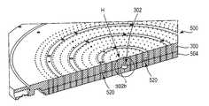
- FIG. 2shows a perspective view of a centering ring 200 (from detail H in FIG. 3 ) which can be used to align a backing plate 300 and showerhead electrode 504 .
- FIG. 3shows a cross sectional perspective view of a showerhead electrode assembly 500 with the centering ring located in opposed channels of the backing plate and the showerhead electrode.
- the fabrication of an integrated circuit chiptypically begins with a thin, polished slice of high-purity, single-crystal semiconductor material substrate (such as silicon or germanium) called a “wafer.” Each wafer is subjected to a sequence of physical and chemical processing steps that form the various circuit structures on the wafer. During the fabrication process, various types of thin films may be deposited on the wafer using various techniques such as thermal oxidation to produce silicon dioxide films, chemical vapor deposition to produce silicon, silicon dioxide, and silicon nitride films, and sputtering or other techniques to produce other metal films.
- various techniquessuch as thermal oxidation to produce silicon dioxide films, chemical vapor deposition to produce silicon, silicon dioxide, and silicon nitride films, and sputtering or other techniques to produce other metal films.
- the unique electrical properties of semiconductorsare produced by substituting selected impurities into the semiconductor crystal lattice using a process called doping.
- the doped silicon wafermay then be uniformly coated with a thin layer of photosensitive, or radiation sensitive material, called a “resist.”
- Small geometric patterns defining the electron paths in the circuitmay then be transferred onto the resist using a process known as lithography.
- the integrated circuit patternmay be drawn on a glass plate called a “mask” and then optically reduced, projected, and transferred onto the photosensitive coating.
- etchingThe lithographed resist pattern is then transferred onto the underlying crystalline surface of the semiconductor material through a process known as etching.
- Vacuum processing chambersare generally used for etching and chemical vapor deposition (CVD) of materials on substrates by supplying an etching or deposition gas to the vacuum chamber and application of a radio frequency (RF) field to the gas to energize the gas into a plasma state.
- RFradio frequency
- a reactive ion etching systemtypically consists of an etching chamber with an upper electrode or anode and a lower electrode or cathode positioned therein.
- the cathodeis negatively biased with respect to the anode and the container walls.
- the wafer to be etchedis covered by a suitable mask and placed directly on the cathode.
- a chemically reactive gassuch as CF 4 , CHF 3 , CClF 3 , HBr, Cl 2 and SF 6 or mixtures thereof with O 2 , N 2 , He or Ar is introduced into the etching chamber and maintained at a pressure which is typically in the millitorr range.
- the upper electrodeis provided with gas hole(s), which permit the gas to be uniformly dispersed through the electrode into the chamber.
- the electric field established between the anode and the cathodewill dissociate the reactive gas forming plasma.
- the surface of the waferis etched by chemical interaction with the active ions and by momentum transfer of the ions striking the surface of the wafer.
- the electric field created by the electrodeswill attract the ions to the cathode, causing the ions to strike the surface in a predominantly vertical direction so that the process produces well-defined vertically etched sidewalls.
- the etching reactor electrodesmay often be fabricated by bonding two or more dissimilar members with mechanically compliant and/or thermally conductive adhesives, allowing for a multiplicity of function.
- FIGS. 1A-Dshow details of showerhead electrode 504 .
- the electrode 504is preferably a plate of high purity (less than 10 ppm impurities) low resistivity (0.005 to 0.02 ohm-cm) single crystal silicon with alignment pin holes 520 in an upper face (mounting surface) 523 which receive alignment pins (not shown) and steps in an outer edge 526 which mate with a clamp ring (not shown) and an inner lip of an outer electrode (not shown).
- Gas holes 528 of suitable diameter and/or configurationextend from the upper face to the lower face (plasma exposed surface) 530 and can be arranged in any suitable pattern.
- a single gas holeis located at the center of the electrode and the remaining gas holes are evenly spaced circumferentially apart in 13 concentric rows with 10 gas holes in the first row located about 0.5 inch from the center of the electrode, 18 gas holes in the second row located about 1 inch from the center, 28 gas holes in the third row located about 1.4 inches from the center, 38 gas holes in the fourth row located about 1.8 inches from the center, 46 gas holes in the fifth row located about 2.3 inches from the center, 56 gas holes in the sixth row located about 2.7 inches from the center, 66 gas holes in the seventh row located about 3.2 inches from the center, 74 gas holes in the eighth row located about 3.6 inches from the center, 84 gas holes in the ninth row located about 4.1 inches from the center, 94 gas holes in the tenth row located about 4.6 inches from the center, 104 gas holes in the eleventh row located about 5.1 inches from the center, 110 gas holes in the twelfth row located about 5.4 inches from the center and 120 holes in the thirteenth row located about 5.7
- a preferred gas hole arrangementhas 40 to 80%, preferably about 60% of the gas holes in an inner zone and 20 to 60%, preferably about 40% of the gas holes in an outer zone separated from the inner zone by a gas seal such as an O-ring.
- a gas sealsuch as an O-ring.
- the upper face of the electrodeincludes 5 alignment pin holes 520 with 2 pin holes near the center and 3 pin holes near the outer edge of the electrode.
- the pin holescan have diameters of about 0.116 inch.
- the 2 central pin holesare radially aligned and are about 0.200 inch deep located about 1.6 inches from the center at locations between the third and fourth row of gas holes.
- the outer pin holesare about 0.100 inch deep and include one pin hole radially aligned with the central pin holes about 6 inches from the center and two other pin holes offset 97.5° and 170° therefrom with the second and the third outer pin holes the same distance from the center but offset 92.5° from each other.
- annular channel 522is located between the center gas hole and the first row of gas holes.
- the channelpreferably has an inner diameter of about 0.24 inch, an outer diameter of about 0.44 inch and depth of about 0.100 inch with an outward taper at the inlet of the channel and an inward taper at the bottom of the channel.
- the outer stepsinclude an inner step 532 and an outer step 534 machined into the silicon plate so as to extend completely around the silicon plate.
- the silicon platehas a thickness of about 0.400 inch and an outer diameter of about 12.560 inch
- the inner step 532has an inner diameter of about 12.004 inches
- the outer step 534has an inner diameter of about 12.135 inches and an outer diameter of about 12.560 inches and extends about 0.24 inch into the plasma exposed surface 530 .
- the inner step 532has a vertical surface 532 a about 0.13 inch long and a horizontal surface 532 b about 0.065 inch long and the outer step 534 has a vertical surface 534 a about 0.11 inch long and a horizontal surface 534 b about 0.218 inch long.
- FIG. 1Bshows a front planar view showing the plasma exposed surface 530 of the electrode 504 with the 13 rows of gas holes.
- FIG. 1Ashows a front planar view of the upper face 523 with the 13 rows of gas holes and 6 pin holes 520 .
- FIG. 1Cshows a side view with the inner step closest to the plasma exposed surface and the outer step closest to the upper face of the electrode.
- FIG. 1Dshows an enlarged view of detail D of FIG.
- 1Cshowing the inner and outer steps with 6 rounded corners provided at the outer edge of the upper face 523 , the outer edge of the lower face 530 and transitions between the horizontal and vertical surfaces 532 a , 532 b , 534 a , 534 b with corners of each other and the upper and lower faces 522 , 530 (e.g., rounded with a 0.025 inch radius).
- FIGS. 1E , F and Gshow cross sections of the showerhead electrode 504 at the outer periphery ( FIG. 1E ), inner zone ( FIG. 1F ) and center ( FIG. 1G ) of the showerhead electrode.
- alignment pin recess 522is aligned with inner step 532 .
- the alignment pin recess 522 in FIG. 1Fis deeper than the pin recess in FIG. 1E and is located between the third and fourth rows of gas outlets.
- the annular channel 522has the same depth as the outer pin recess 520 and the channel 522 is concentric around the center gas outlet 528 .
- FIG. 2is an enlarged view of a centering ring 200 (from detail H of FIG. 3 ) which can be used to align the showerhead electrode 504 with a backing plate 300 .
- the ring 200is preferably configured such that an inner wall 200 a of the ring 200 provides a friction fit with the inner wall 522 a of channel 522 and the outer wall 200 b of the ring 200 provides a friction fit with the outer wall 302 b of channel 302 in backing plate 300 .
- the ringmay also provide a gas seal between the electrode 504 and backing plate 300 .
- the ring 200is preferably of a dielectric material such as “TORLON 5030” which is compatible with the elevated temperatures and high purity requirements in semiconductor processing environments.
- the ring 200is preferably configured to (a) center against the outer wall 302 b of the annular channel 302 in the aluminum backing plate 300 and (b) center against the inner wall 522 a of the annular channel 522 in the silicon electrode.
- the electrode 504 and backing plate 300heat up and differential thermal expansion places high loads on the ring 200 .
- the ring 200is tapered at its top and bottom and channels 522 , 302 include similar tapers which mate with the tapers on the ring.
- the ring 200bears against the inner wall 522 a of channel 522 and outer wall 302 b of channel 302 and the outer wall 522 b of channel 522 need not frictionally engage the outer wall 200 b of the ring 200 and the inner wall (not shown) of the channel 302 need not frictionally engage the inner wall 200 a of ring 200 .
- the ring 200disengages the inner wall 522 a of channel 522 and instead bears against the inner wall (not shown) of channel 302 in the backing plate.
- alignment of the gas holes in the showerhead electrode with the gas outlets in the backing platecan be maintained.
Landscapes
- Physics & Mathematics (AREA)
- Engineering & Computer Science (AREA)
- Plasma & Fusion (AREA)
- Chemical & Material Sciences (AREA)
- Analytical Chemistry (AREA)
- Drying Of Semiconductors (AREA)
- Plasma Technology (AREA)
- Chemical Vapour Deposition (AREA)
Abstract
Description
The invention relates to a showerhead electrode used as an upper electrode in a plasma processing chamber in which semiconductor components can be manufactured. The showerhead electrode can be clamped to a backing plate with a clamp ring as described in U.S. application Ser. No. 12/216,526 entitled Clamped Showerhead Electrode Assembly, filed Jul. 7, 2008, the entire content of which is hereby incorporated by reference.
A showerhead electrode used as an upper electrode of a capacitively coupled plasma processing chamber comprises a circular plate having a plasma exposed surface on a lower face thereof and a mounting surface on an upper face thereof. The lower face includes inner and outer steps at an outer periphery of the plate. The inner step has a smaller diameter than the outer step and the outer step is located between the inner step and the mounting surface. The outer step is configured to mate with an inwardly extending flange of a clamp ring and the inner step is configured to mate with an inner step of an outer electrode which surrounds the showerhead electrode such that an inner tapered surface of the outer electrode extends from the outer edge of the plasma exposed surface. The mounting surface includes an annular channel configured to receive a centering ring and a plurality of alignment pin recesses configured to receive alignment pins arranged in a pattern matching alignment pin holes in a backing plate against which the plate is held by the clamp ring and the plate includes process gas outlets arranged in a pattern matching gas supply holes in the backing plate.
The fabrication of an integrated circuit chip typically begins with a thin, polished slice of high-purity, single-crystal semiconductor material substrate (such as silicon or germanium) called a “wafer.” Each wafer is subjected to a sequence of physical and chemical processing steps that form the various circuit structures on the wafer. During the fabrication process, various types of thin films may be deposited on the wafer using various techniques such as thermal oxidation to produce silicon dioxide films, chemical vapor deposition to produce silicon, silicon dioxide, and silicon nitride films, and sputtering or other techniques to produce other metal films.
After depositing a film on the semiconductor wafer, the unique electrical properties of semiconductors are produced by substituting selected impurities into the semiconductor crystal lattice using a process called doping. The doped silicon wafer may then be uniformly coated with a thin layer of photosensitive, or radiation sensitive material, called a “resist.” Small geometric patterns defining the electron paths in the circuit may then be transferred onto the resist using a process known as lithography. During the lithographic process, the integrated circuit pattern may be drawn on a glass plate called a “mask” and then optically reduced, projected, and transferred onto the photosensitive coating.
The lithographed resist pattern is then transferred onto the underlying crystalline surface of the semiconductor material through a process known as etching. Vacuum processing chambers are generally used for etching and chemical vapor deposition (CVD) of materials on substrates by supplying an etching or deposition gas to the vacuum chamber and application of a radio frequency (RF) field to the gas to energize the gas into a plasma state.
A reactive ion etching system typically consists of an etching chamber with an upper electrode or anode and a lower electrode or cathode positioned therein. The cathode is negatively biased with respect to the anode and the container walls. The wafer to be etched is covered by a suitable mask and placed directly on the cathode. A chemically reactive gas such as CF4, CHF3, CClF3, HBr, Cl2and SF6or mixtures thereof with O2, N2, He or Ar is introduced into the etching chamber and maintained at a pressure which is typically in the millitorr range. The upper electrode is provided with gas hole(s), which permit the gas to be uniformly dispersed through the electrode into the chamber. The electric field established between the anode and the cathode will dissociate the reactive gas forming plasma. The surface of the wafer is etched by chemical interaction with the active ions and by momentum transfer of the ions striking the surface of the wafer. The electric field created by the electrodes will attract the ions to the cathode, causing the ions to strike the surface in a predominantly vertical direction so that the process produces well-defined vertically etched sidewalls. The etching reactor electrodes may often be fabricated by bonding two or more dissimilar members with mechanically compliant and/or thermally conductive adhesives, allowing for a multiplicity of function.
A preferred gas hole arrangement has 40 to 80%, preferably about 60% of the gas holes in an inner zone and 20 to 60%, preferably about 40% of the gas holes in an outer zone separated from the inner zone by a gas seal such as an O-ring. Thus, inner and outer zones above a wafer undergoing plasma etching can be fed the same or different etch gas at the same or different flow rates to optimize etch uniformity.
The upper face of the electrode includes 5alignment pin holes 520 with 2 pin holes near the center and 3 pin holes near the outer edge of the electrode. The pin holes can have diameters of about 0.116 inch. The 2 central pin holes are radially aligned and are about 0.200 inch deep located about 1.6 inches from the center at locations between the third and fourth row of gas holes. The outer pin holes are about 0.100 inch deep and include one pin hole radially aligned with the central pin holes about 6 inches from the center and two other pin holes offset 97.5° and 170° therefrom with the second and the third outer pin holes the same distance from the center but offset 92.5° from each other.
For receipt of a centering ring, anannular channel 522 is located between the center gas hole and the first row of gas holes. The channel preferably has an inner diameter of about 0.24 inch, an outer diameter of about 0.44 inch and depth of about 0.100 inch with an outward taper at the inlet of the channel and an inward taper at the bottom of the channel.
The outer steps include aninner step 532 and anouter step 534 machined into the silicon plate so as to extend completely around the silicon plate. In a preferred embodiment, the silicon plate has a thickness of about 0.400 inch and an outer diameter of about 12.560 inch, theinner step 532 has an inner diameter of about 12.004 inches, an outer diameter of about 12.135 inch and extends about 0.13 inch into the plasma exposedsurface 530 and theouter step 534 has an inner diameter of about 12.135 inches and an outer diameter of about 12.560 inches and extends about 0.24 inch into the plasma exposedsurface 530. Theinner step 532 has avertical surface 532aabout 0.13 inch long and ahorizontal surface 532babout 0.065 inch long and theouter step 534 has avertical surface 534aabout 0.11 inch long and ahorizontal surface 534babout 0.218 inch long.
Thering 200 is preferably of a dielectric material such as “TORLON 5030” which is compatible with the elevated temperatures and high purity requirements in semiconductor processing environments. Thering 200 is preferably configured to (a) center against theouter wall 302bof theannular channel 302 in thealuminum backing plate 300 and (b) center against theinner wall 522aof theannular channel 522 in the silicon electrode. During wafer processing such as plasma etching, theelectrode 504 andbacking plate 300 heat up and differential thermal expansion places high loads on thering 200. To accommodate the thermal stresses, thering 200 is tapered at its top and bottom andchannels ring 200 bears against theinner wall 522aofchannel 522 andouter wall 302bofchannel 302 and theouter wall 522bofchannel 522 need not frictionally engage theouter wall 200bof thering 200 and the inner wall (not shown) of thechannel 302 need not frictionally engage theinner wall 200aofring 200. However, as thesilicon electrode 504 and aluminum backing plate heat up, thering 200 disengages theinner wall 522aofchannel 522 and instead bears against the inner wall (not shown) ofchannel 302 in the backing plate. Thus, alignment of the gas holes in the showerhead electrode with the gas outlets in the backing plate can be maintained.
While the invention has been described in detail with reference to specific embodiments thereof, it will be apparent to those skilled in the art that various changes and modifications can be made, and equivalents employed, without departing from the scope of the appended claims.
Claims (14)
1. A showerhead electrode for use as an upper electrode of a capacitively coupled plasma processing chamber, comprising:
a circular plate having a plasma exposed surface on a lower face thereof, a mounting surface on an upper face thereof;
the mounting surface including an annular channel configured to receive a centering ring and a plurality of alignment pin recesses configured to receive alignment pins arranged in a pattern matching alignment pin holes in a backing plate;
the circular plate including process gas outlets arranged in a pattern matching gas supply holes in the backing plate, the gas outlets communicating with gas passages extending between the upper and lower faces.
2. The electrode ofclaim 1 , wherein the annular channel is located between a center gas outlet at the center of the circular plate and a row of circumferentially spaced apart gas outlets and the alignment pin recesses include at least one intermediate pin recess on opposite sides of the annular channel, and a plurality of pin recesses circumferentially spaced apart in an outer zone of the upper face.
3. The electrode ofclaim 1 , wherein the circular plate is of single crystal silicon.
4. The electrode ofclaim 1 , wherein the gas outlets include a pattern of 13 circumferential rows.
5. The electrode ofclaim 4 , wherein the 13 circumferential rows include 10 inner rows equally spaced apart by a distance greater than the distance separating the 3 outer rows.
6. The electrode ofclaim 1 , wherein the lower face includes inner and outer steps at an outer periphery of the circular plate and the inner step having a smaller diameter than the outer step and the outer step being located between the inner step and the mounting surface, the outer step includes a horizontal surface which extends inwardly from the outer periphery by a first distance, the inner step includes a horizontal surface which extends inward from the outer step by a second distance, the first distance being at least two times larger than the second distance.
7. The electrode ofclaim 6 , wherein the circular plate has parallel upper and lower faces with a thickness between the upper and lower faces of no greater than 0.5 inch, the horizontal surface of the outer step is spaced from the upper face by a first vertical distance, the horizontal surface of the inner step is spaced from the lower face by a second vertical distance, and the horizontal surface of the outer step is separated from the horizontal surface of the inner step by a third distance, the first vertical distance being greater than the second vertical distance and the second vertical distance being greater than the third vertical distance.
8. The electrode ofclaim 1 , wherein the annular channel has an inner diameter of about 0.24 inch, an outer diameter of about 0.44 inch and a depth of about 0.1 inch.
9. A showerhead electrode assembly comprising the electrode ofclaim 1 , a backing plate and a centering ring, the backing plate including an annular channel configured to receive the centering ring and an inner wall of the centering ring being frictionally engaged with an inner wall of the annular channel in the showerhead electrode and an outer wall of the centering ring being frictionally engaged with an outer wall of the annular channel in the backing plate at ambient temperature.
10. The electrode assembly ofclaim 9 , wherein the showerhead electrode is silicon and the backing plate is aluminum, the showerhead electrode assembly being operable at temperatures of 20 to 200° C. and the centering ring being of a material which expands more than the silicon such that a lower portion of the inner wall of the centering ring disengages from the inner wall of the channel in the showerhead electrode while an upper portion of the inner wall of the centering ring frictionally engages the inner wall of the channel in the backing plate to thereby maintain alignment of gas holes in the showerhead electrode and the backing plate.
11. A centering ring operable to frictionally hold a backing plate to a showerhead electrode, the centering ring being of a polymer material with a height of about 0.3 inch, inner diameter of about 0.24 inch and outer diameter of about 0.44 inch.
12. The centering ring ofclaim 11 , wherein an inner wall of the centering ring is operable to frictionally engage an inner wall of an annular channel in the showerhead electrode and an outer wall of the centering ring is operable to frictionally engage an outer wall of an annular channel in the backing plate at ambient temperature.
13. The centering ring ofclaim 12 , wherein the centering ring is of a material which expands more than the showerhead electrode so that a lower portion of the inner wall of the centering ring disengages from the inner wall of the channel in the showerhead electrode while an upper portion of the inner wall of the centering ring frictionally engages the inner wall of the channel in the backing plate.
14. A showerhead electrode ofclaim 1 , wherein the lower face includes inner and outer steps at an outer periphery of the plate and the inner step having a smaller diameter than the outer step and the outer step being located between the inner step and the mounting surface.
Priority Applications (5)
| Application Number | Priority Date | Filing Date | Title |
|---|---|---|---|
| US12/419,878US8402918B2 (en) | 2009-04-07 | 2009-04-07 | Showerhead electrode with centering feature |
| JP2010002240UJP3162880U (en) | 2009-04-07 | 2010-04-02 | Shower head electrode with centering function |
| KR2020100003580UKR200468262Y1 (en) | 2009-04-07 | 2010-04-06 | Showerhead electrode with centering feature |
| TW099206024UTWM397124U (en) | 2009-04-07 | 2010-04-06 | Showerhead electrode, showerhead electrode assembly, and centering ring |
| CN2010201760428UCN201898113U (en) | 2009-04-07 | 2010-04-07 | Spray header electrode with centralized positioning characteristic and spray header electrode assembly |
Applications Claiming Priority (1)
| Application Number | Priority Date | Filing Date | Title |
|---|---|---|---|
| US12/419,878US8402918B2 (en) | 2009-04-07 | 2009-04-07 | Showerhead electrode with centering feature |
Publications (2)
| Publication Number | Publication Date |
|---|---|
| US20100252197A1 US20100252197A1 (en) | 2010-10-07 |
| US8402918B2true US8402918B2 (en) | 2013-03-26 |
Family
ID=42825209
Family Applications (1)
| Application Number | Title | Priority Date | Filing Date |
|---|---|---|---|
| US12/419,878Active2031-09-27US8402918B2 (en) | 2009-04-07 | 2009-04-07 | Showerhead electrode with centering feature |
Country Status (5)
| Country | Link |
|---|---|
| US (1) | US8402918B2 (en) |
| JP (1) | JP3162880U (en) |
| KR (1) | KR200468262Y1 (en) |
| CN (1) | CN201898113U (en) |
| TW (1) | TWM397124U (en) |
Cited By (332)
| Publication number | Priority date | Publication date | Assignee | Title |
|---|---|---|---|---|
| US20120055632A1 (en)* | 2010-09-03 | 2012-03-08 | Lam Research Corporation | Showerhead electrode |
| US20130133580A1 (en)* | 2011-11-29 | 2013-05-30 | Intermolecular, Inc. | High productivity vapor processing system |
| US8796153B2 (en) | 2008-07-07 | 2014-08-05 | Lam Research Corporation | Clamped monolithic showerhead electrode |
| USD787458S1 (en)* | 2015-11-18 | 2017-05-23 | Asm Ip Holding B.V. | Gas supply plate for semiconductor manufacturing apparatus |
| USD793572S1 (en)* | 2015-06-10 | 2017-08-01 | Tokyo Electron Limited | Electrode plate for plasma processing apparatus |
| US9911579B2 (en)* | 2014-07-03 | 2018-03-06 | Applied Materials, Inc. | Showerhead having a detachable high resistivity gas distribution plate |
| USD829306S1 (en)* | 2016-07-06 | 2018-09-25 | Asm Ip Holding B.V. | Shower plate |
| USD834686S1 (en)* | 2016-12-15 | 2018-11-27 | Asm Ip Holding B.V. | Shower plate |
| US10262834B2 (en) | 2009-10-13 | 2019-04-16 | Lam Research Corporation | Edge-clamped and mechanically fastened inner electrode of showerhead electrode assembly |
| US20190284695A1 (en)* | 2018-03-15 | 2019-09-19 | Taiwan Semiconductor Manufacturing Company Ltd. | Film formation apparatus and method for forming semiconductor structure |
| US10559458B1 (en) | 2018-11-26 | 2020-02-11 | Asm Ip Holding B.V. | Method of forming oxynitride film |
| US10561975B2 (en) | 2014-10-07 | 2020-02-18 | Asm Ip Holdings B.V. | Variable conductance gas distribution apparatus and method |
| USD876504S1 (en) | 2017-04-03 | 2020-02-25 | Asm Ip Holding B.V. | Exhaust flow control ring for semiconductor deposition apparatus |
| US10590535B2 (en) | 2017-07-26 | 2020-03-17 | Asm Ip Holdings B.V. | Chemical treatment, deposition and/or infiltration apparatus and method for using the same |
| US10600673B2 (en) | 2015-07-07 | 2020-03-24 | Asm Ip Holding B.V. | Magnetic susceptor to baseplate seal |
| US10604847B2 (en) | 2014-03-18 | 2020-03-31 | Asm Ip Holding B.V. | Gas distribution system, reactor including the system, and methods of using the same |
| USD880437S1 (en)* | 2018-02-01 | 2020-04-07 | Asm Ip Holding B.V. | Gas supply plate for semiconductor manufacturing apparatus |
| US10612136B2 (en) | 2018-06-29 | 2020-04-07 | ASM IP Holding, B.V. | Temperature-controlled flange and reactor system including same |
| US10622375B2 (en) | 2016-11-07 | 2020-04-14 | Asm Ip Holding B.V. | Method of processing a substrate and a device manufactured by using the method |
| US10643826B2 (en) | 2016-10-26 | 2020-05-05 | Asm Ip Holdings B.V. | Methods for thermally calibrating reaction chambers |
| US10643904B2 (en) | 2016-11-01 | 2020-05-05 | Asm Ip Holdings B.V. | Methods for forming a semiconductor device and related semiconductor device structures |
| US10655221B2 (en) | 2017-02-09 | 2020-05-19 | Asm Ip Holding B.V. | Method for depositing oxide film by thermal ALD and PEALD |
| US10658205B2 (en) | 2017-09-28 | 2020-05-19 | Asm Ip Holdings B.V. | Chemical dispensing apparatus and methods for dispensing a chemical to a reaction chamber |
| US10658181B2 (en) | 2018-02-20 | 2020-05-19 | Asm Ip Holding B.V. | Method of spacer-defined direct patterning in semiconductor fabrication |
| US10665452B2 (en) | 2016-05-02 | 2020-05-26 | Asm Ip Holdings B.V. | Source/drain performance through conformal solid state doping |
| US10672636B2 (en) | 2017-08-09 | 2020-06-02 | Asm Ip Holding B.V. | Cassette holder assembly for a substrate cassette and holding member for use in such assembly |
| US10685834B2 (en) | 2017-07-05 | 2020-06-16 | Asm Ip Holdings B.V. | Methods for forming a silicon germanium tin layer and related semiconductor device structures |
| US10683571B2 (en) | 2014-02-25 | 2020-06-16 | Asm Ip Holding B.V. | Gas supply manifold and method of supplying gases to chamber using same |
| US10692741B2 (en) | 2017-08-08 | 2020-06-23 | Asm Ip Holdings B.V. | Radiation shield |
| US10707106B2 (en) | 2011-06-06 | 2020-07-07 | Asm Ip Holding B.V. | High-throughput semiconductor-processing apparatus equipped with multiple dual-chamber modules |
| US10714315B2 (en) | 2012-10-12 | 2020-07-14 | Asm Ip Holdings B.V. | Semiconductor reaction chamber showerhead |
| US10714350B2 (en) | 2016-11-01 | 2020-07-14 | ASM IP Holdings, B.V. | Methods for forming a transition metal niobium nitride film on a substrate by atomic layer deposition and related semiconductor device structures |
| US10714385B2 (en) | 2016-07-19 | 2020-07-14 | Asm Ip Holding B.V. | Selective deposition of tungsten |
| US10714335B2 (en) | 2017-04-25 | 2020-07-14 | Asm Ip Holding B.V. | Method of depositing thin film and method of manufacturing semiconductor device |
| US10720331B2 (en) | 2016-11-01 | 2020-07-21 | ASM IP Holdings, B.V. | Methods for forming a transition metal nitride film on a substrate by atomic layer deposition and related semiconductor device structures |
| US10720322B2 (en) | 2016-02-19 | 2020-07-21 | Asm Ip Holding B.V. | Method for forming silicon nitride film selectively on top surface |
| US10734497B2 (en) | 2017-07-18 | 2020-08-04 | Asm Ip Holding B.V. | Methods for forming a semiconductor device structure and related semiconductor device structures |
| US10731249B2 (en) | 2018-02-15 | 2020-08-04 | Asm Ip Holding B.V. | Method of forming a transition metal containing film on a substrate by a cyclical deposition process, a method for supplying a transition metal halide compound to a reaction chamber, and related vapor deposition apparatus |
| US10734223B2 (en) | 2017-10-10 | 2020-08-04 | Asm Ip Holding B.V. | Method for depositing a metal chalcogenide on a substrate by cyclical deposition |
| US10734244B2 (en) | 2017-11-16 | 2020-08-04 | Asm Ip Holding B.V. | Method of processing a substrate and a device manufactured by the same |
| US10741385B2 (en) | 2016-07-28 | 2020-08-11 | Asm Ip Holding B.V. | Method and apparatus for filling a gap |
| US10755922B2 (en) | 2018-07-03 | 2020-08-25 | Asm Ip Holding B.V. | Method for depositing silicon-free carbon-containing film as gap-fill layer by pulse plasma-assisted deposition |
| US10755923B2 (en) | 2018-07-03 | 2020-08-25 | Asm Ip Holding B.V. | Method for depositing silicon-free carbon-containing film as gap-fill layer by pulse plasma-assisted deposition |
| US10770336B2 (en) | 2017-08-08 | 2020-09-08 | Asm Ip Holding B.V. | Substrate lift mechanism and reactor including same |
| US10767789B2 (en) | 2018-07-16 | 2020-09-08 | Asm Ip Holding B.V. | Diaphragm valves, valve components, and methods for forming valve components |
| US10770286B2 (en) | 2017-05-08 | 2020-09-08 | Asm Ip Holdings B.V. | Methods for selectively forming a silicon nitride film on a substrate and related semiconductor device structures |
| US10784102B2 (en) | 2016-12-22 | 2020-09-22 | Asm Ip Holding B.V. | Method of forming a structure on a substrate |
| US10787741B2 (en) | 2014-08-21 | 2020-09-29 | Asm Ip Holding B.V. | Method and system for in situ formation of gas-phase compounds |
| US10797133B2 (en) | 2018-06-21 | 2020-10-06 | Asm Ip Holding B.V. | Method for depositing a phosphorus doped silicon arsenide film and related semiconductor device structures |
| US10801106B2 (en) | 2016-12-15 | 2020-10-13 | Asm Ip Holding B.V. | Shower plate structure for exhausting deposition inhibiting gas |
| US10804098B2 (en) | 2009-08-14 | 2020-10-13 | Asm Ip Holding B.V. | Systems and methods for thin-film deposition of metal oxides using excited nitrogen-oxygen species |
| US10811256B2 (en) | 2018-10-16 | 2020-10-20 | Asm Ip Holding B.V. | Method for etching a carbon-containing feature |
| USD900036S1 (en) | 2017-08-24 | 2020-10-27 | Asm Ip Holding B.V. | Heater electrical connector and adapter |
| US10818758B2 (en) | 2018-11-16 | 2020-10-27 | Asm Ip Holding B.V. | Methods for forming a metal silicate film on a substrate in a reaction chamber and related semiconductor device structures |
| US10829852B2 (en) | 2018-08-16 | 2020-11-10 | Asm Ip Holding B.V. | Gas distribution device for a wafer processing apparatus |
| US10832903B2 (en) | 2011-10-28 | 2020-11-10 | Asm Ip Holding B.V. | Process feed management for semiconductor substrate processing |
| US10847366B2 (en) | 2018-11-16 | 2020-11-24 | Asm Ip Holding B.V. | Methods for depositing a transition metal chalcogenide film on a substrate by a cyclical deposition process |
| US10844484B2 (en) | 2017-09-22 | 2020-11-24 | Asm Ip Holding B.V. | Apparatus for dispensing a vapor phase reactant to a reaction chamber and related methods |
| US10844486B2 (en) | 2009-04-06 | 2020-11-24 | Asm Ip Holding B.V. | Semiconductor processing reactor and components thereof |
| US10847371B2 (en) | 2018-03-27 | 2020-11-24 | Asm Ip Holding B.V. | Method of forming an electrode on a substrate and a semiconductor device structure including an electrode |
| US10847365B2 (en) | 2018-10-11 | 2020-11-24 | Asm Ip Holding B.V. | Method of forming conformal silicon carbide film by cyclic CVD |
| US10851456B2 (en) | 2016-04-21 | 2020-12-01 | Asm Ip Holding B.V. | Deposition of metal borides |
| USD903477S1 (en) | 2018-01-24 | 2020-12-01 | Asm Ip Holdings B.V. | Metal clamp |
| US10854498B2 (en) | 2011-07-15 | 2020-12-01 | Asm Ip Holding B.V. | Wafer-supporting device and method for producing same |
| US10858737B2 (en) | 2014-07-28 | 2020-12-08 | Asm Ip Holding B.V. | Showerhead assembly and components thereof |
| US10867788B2 (en) | 2016-12-28 | 2020-12-15 | Asm Ip Holding B.V. | Method of forming a structure on a substrate |
| US10865475B2 (en) | 2016-04-21 | 2020-12-15 | Asm Ip Holding B.V. | Deposition of metal borides and silicides |
| US10867786B2 (en) | 2018-03-30 | 2020-12-15 | Asm Ip Holding B.V. | Substrate processing method |
| US10872771B2 (en) | 2018-01-16 | 2020-12-22 | Asm Ip Holding B. V. | Method for depositing a material film on a substrate within a reaction chamber by a cyclical deposition process and related device structures |
| US10883175B2 (en) | 2018-08-09 | 2021-01-05 | Asm Ip Holding B.V. | Vertical furnace for processing substrates and a liner for use therein |
| US10892156B2 (en) | 2017-05-08 | 2021-01-12 | Asm Ip Holding B.V. | Methods for forming a silicon nitride film on a substrate and related semiconductor device structures |
| US10896820B2 (en) | 2018-02-14 | 2021-01-19 | Asm Ip Holding B.V. | Method for depositing a ruthenium-containing film on a substrate by a cyclical deposition process |
| US10910262B2 (en) | 2017-11-16 | 2021-02-02 | Asm Ip Holding B.V. | Method of selectively depositing a capping layer structure on a semiconductor device structure |
| US10914004B2 (en) | 2018-06-29 | 2021-02-09 | Asm Ip Holding B.V. | Thin-film deposition method and manufacturing method of semiconductor device |
| US10923344B2 (en) | 2017-10-30 | 2021-02-16 | Asm Ip Holding B.V. | Methods for forming a semiconductor structure and related semiconductor structures |
| US10928731B2 (en) | 2017-09-21 | 2021-02-23 | Asm Ip Holding B.V. | Method of sequential infiltration synthesis treatment of infiltrateable material and structures and devices formed using same |
| US10934619B2 (en) | 2016-11-15 | 2021-03-02 | Asm Ip Holding B.V. | Gas supply unit and substrate processing apparatus including the gas supply unit |
| USD911985S1 (en)* | 2018-06-08 | 2021-03-02 | Tokyo Electron Limited | Gas introduction plate for plasma etching apparatus for etching semiconductor wafer |
| US10941490B2 (en) | 2014-10-07 | 2021-03-09 | Asm Ip Holding B.V. | Multiple temperature range susceptor, assembly, reactor and system including the susceptor, and methods of using the same |
| US10975470B2 (en) | 2018-02-23 | 2021-04-13 | Asm Ip Holding B.V. | Apparatus for detecting or monitoring for a chemical precursor in a high temperature environment |
| US11001925B2 (en) | 2016-12-19 | 2021-05-11 | Asm Ip Holding B.V. | Substrate processing apparatus |
| US11004977B2 (en) | 2017-07-19 | 2021-05-11 | Asm Ip Holding B.V. | Method for depositing a group IV semiconductor and related semiconductor device structures |
| US11018002B2 (en) | 2017-07-19 | 2021-05-25 | Asm Ip Holding B.V. | Method for selectively depositing a Group IV semiconductor and related semiconductor device structures |
| US11018047B2 (en) | 2018-01-25 | 2021-05-25 | Asm Ip Holding B.V. | Hybrid lift pin |
| US11015245B2 (en) | 2014-03-19 | 2021-05-25 | Asm Ip Holding B.V. | Gas-phase reactor and system having exhaust plenum and components thereof |
| US11022879B2 (en) | 2017-11-24 | 2021-06-01 | Asm Ip Holding B.V. | Method of forming an enhanced unexposed photoresist layer |
| US11024523B2 (en) | 2018-09-11 | 2021-06-01 | Asm Ip Holding B.V. | Substrate processing apparatus and method |
| US11031242B2 (en) | 2018-11-07 | 2021-06-08 | Asm Ip Holding B.V. | Methods for depositing a boron doped silicon germanium film |
| USD922229S1 (en) | 2019-06-05 | 2021-06-15 | Asm Ip Holding B.V. | Device for controlling a temperature of a gas supply unit |
| US11049751B2 (en) | 2018-09-14 | 2021-06-29 | Asm Ip Holding B.V. | Cassette supply system to store and handle cassettes and processing apparatus equipped therewith |
| US11053591B2 (en) | 2018-08-06 | 2021-07-06 | Asm Ip Holding B.V. | Multi-port gas injection system and reactor system including same |
| US11056344B2 (en) | 2017-08-30 | 2021-07-06 | Asm Ip Holding B.V. | Layer forming method |
| US11056567B2 (en) | 2018-05-11 | 2021-07-06 | Asm Ip Holding B.V. | Method of forming a doped metal carbide film on a substrate and related semiconductor device structures |
| US11069510B2 (en) | 2017-08-30 | 2021-07-20 | Asm Ip Holding B.V. | Substrate processing apparatus |
| US11081345B2 (en) | 2018-02-06 | 2021-08-03 | Asm Ip Holding B.V. | Method of post-deposition treatment for silicon oxide film |
| US11088002B2 (en) | 2018-03-29 | 2021-08-10 | Asm Ip Holding B.V. | Substrate rack and a substrate processing system and method |
| US11087997B2 (en) | 2018-10-31 | 2021-08-10 | Asm Ip Holding B.V. | Substrate processing apparatus for processing substrates |
| US11094582B2 (en) | 2016-07-08 | 2021-08-17 | Asm Ip Holding B.V. | Selective deposition method to form air gaps |
| US11094546B2 (en) | 2017-10-05 | 2021-08-17 | Asm Ip Holding B.V. | Method for selectively depositing a metallic film on a substrate |
| US11101370B2 (en) | 2016-05-02 | 2021-08-24 | Asm Ip Holding B.V. | Method of forming a germanium oxynitride film |
| US11114283B2 (en) | 2018-03-16 | 2021-09-07 | Asm Ip Holding B.V. | Reactor, system including the reactor, and methods of manufacturing and using same |
| US11114294B2 (en) | 2019-03-08 | 2021-09-07 | Asm Ip Holding B.V. | Structure including SiOC layer and method of forming same |
| USD930782S1 (en) | 2019-08-22 | 2021-09-14 | Asm Ip Holding B.V. | Gas distributor |
| US11127617B2 (en) | 2017-11-27 | 2021-09-21 | Asm Ip Holding B.V. | Storage device for storing wafer cassettes for use with a batch furnace |
| US11127589B2 (en) | 2019-02-01 | 2021-09-21 | Asm Ip Holding B.V. | Method of topology-selective film formation of silicon oxide |
| USD931978S1 (en) | 2019-06-27 | 2021-09-28 | Asm Ip Holding B.V. | Showerhead vacuum transport |
| US11139191B2 (en) | 2017-08-09 | 2021-10-05 | Asm Ip Holding B.V. | Storage apparatus for storing cassettes for substrates and processing apparatus equipped therewith |
| US11139308B2 (en) | 2015-12-29 | 2021-10-05 | Asm Ip Holding B.V. | Atomic layer deposition of III-V compounds to form V-NAND devices |
| US11158513B2 (en) | 2018-12-13 | 2021-10-26 | Asm Ip Holding B.V. | Methods for forming a rhenium-containing film on a substrate by a cyclical deposition process and related semiconductor device structures |
| US11171025B2 (en) | 2019-01-22 | 2021-11-09 | Asm Ip Holding B.V. | Substrate processing device |
| USD935572S1 (en) | 2019-05-24 | 2021-11-09 | Asm Ip Holding B.V. | Gas channel plate |
| US11205585B2 (en) | 2016-07-28 | 2021-12-21 | Asm Ip Holding B.V. | Substrate processing apparatus and method of operating the same |
| US11217444B2 (en) | 2018-11-30 | 2022-01-04 | Asm Ip Holding B.V. | Method for forming an ultraviolet radiation responsive metal oxide-containing film |
| US11222772B2 (en) | 2016-12-14 | 2022-01-11 | Asm Ip Holding B.V. | Substrate processing apparatus |
| USD940837S1 (en) | 2019-08-22 | 2022-01-11 | Asm Ip Holding B.V. | Electrode |
| US11227782B2 (en) | 2019-07-31 | 2022-01-18 | Asm Ip Holding B.V. | Vertical batch furnace assembly |
| US11227789B2 (en) | 2019-02-20 | 2022-01-18 | Asm Ip Holding B.V. | Method and apparatus for filling a recess formed within a substrate surface |
| US11230766B2 (en) | 2018-03-29 | 2022-01-25 | Asm Ip Holding B.V. | Substrate processing apparatus and method |
| US11232963B2 (en) | 2018-10-03 | 2022-01-25 | Asm Ip Holding B.V. | Substrate processing apparatus and method |
| US11233133B2 (en) | 2015-10-21 | 2022-01-25 | Asm Ip Holding B.V. | NbMC layers |
| US11242598B2 (en) | 2015-06-26 | 2022-02-08 | Asm Ip Holding B.V. | Structures including metal carbide material, devices including the structures, and methods of forming same |
| US11251040B2 (en) | 2019-02-20 | 2022-02-15 | Asm Ip Holding B.V. | Cyclical deposition method including treatment step and apparatus for same |
| US11251068B2 (en) | 2018-10-19 | 2022-02-15 | Asm Ip Holding B.V. | Substrate processing apparatus and substrate processing method |
| USD944946S1 (en) | 2019-06-14 | 2022-03-01 | Asm Ip Holding B.V. | Shower plate |
| US11270899B2 (en) | 2018-06-04 | 2022-03-08 | Asm Ip Holding B.V. | Wafer handling chamber with moisture reduction |
| US11274369B2 (en) | 2018-09-11 | 2022-03-15 | Asm Ip Holding B.V. | Thin film deposition method |
| US11282698B2 (en) | 2019-07-19 | 2022-03-22 | Asm Ip Holding B.V. | Method of forming topology-controlled amorphous carbon polymer film |
| US11289326B2 (en) | 2019-05-07 | 2022-03-29 | Asm Ip Holding B.V. | Method for reforming amorphous carbon polymer film |
| US11286562B2 (en) | 2018-06-08 | 2022-03-29 | Asm Ip Holding B.V. | Gas-phase chemical reactor and method of using same |
| US11286558B2 (en) | 2019-08-23 | 2022-03-29 | Asm Ip Holding B.V. | Methods for depositing a molybdenum nitride film on a surface of a substrate by a cyclical deposition process and related semiconductor device structures including a molybdenum nitride film |
| USD947913S1 (en) | 2019-05-17 | 2022-04-05 | Asm Ip Holding B.V. | Susceptor shaft |
| US11295980B2 (en) | 2017-08-30 | 2022-04-05 | Asm Ip Holding B.V. | Methods for depositing a molybdenum metal film over a dielectric surface of a substrate by a cyclical deposition process and related semiconductor device structures |
| USD948463S1 (en) | 2018-10-24 | 2022-04-12 | Asm Ip Holding B.V. | Susceptor for semiconductor substrate supporting apparatus |
| US11306395B2 (en) | 2017-06-28 | 2022-04-19 | Asm Ip Holding B.V. | Methods for depositing a transition metal nitride film on a substrate by atomic layer deposition and related deposition apparatus |
| USD949319S1 (en) | 2019-08-22 | 2022-04-19 | Asm Ip Holding B.V. | Exhaust duct |
| US11315794B2 (en) | 2019-10-21 | 2022-04-26 | Asm Ip Holding B.V. | Apparatus and methods for selectively etching films |
| US11339476B2 (en) | 2019-10-08 | 2022-05-24 | Asm Ip Holding B.V. | Substrate processing device having connection plates, substrate processing method |
| US11342216B2 (en) | 2019-02-20 | 2022-05-24 | Asm Ip Holding B.V. | Cyclical deposition method and apparatus for filling a recess formed within a substrate surface |
| US11345999B2 (en) | 2019-06-06 | 2022-05-31 | Asm Ip Holding B.V. | Method of using a gas-phase reactor system including analyzing exhausted gas |
| US11355338B2 (en) | 2019-05-10 | 2022-06-07 | Asm Ip Holding B.V. | Method of depositing material onto a surface and structure formed according to the method |
| US11361990B2 (en) | 2018-05-28 | 2022-06-14 | Asm Ip Holding B.V. | Substrate processing method and device manufactured by using the same |
| US11374112B2 (en) | 2017-07-19 | 2022-06-28 | Asm Ip Holding B.V. | Method for depositing a group IV semiconductor and related semiconductor device structures |
| US11378337B2 (en) | 2019-03-28 | 2022-07-05 | Asm Ip Holding B.V. | Door opener and substrate processing apparatus provided therewith |
| US11393690B2 (en) | 2018-01-19 | 2022-07-19 | Asm Ip Holding B.V. | Deposition method |
| US11390950B2 (en) | 2017-01-10 | 2022-07-19 | Asm Ip Holding B.V. | Reactor system and method to reduce residue buildup during a film deposition process |
| US11390945B2 (en) | 2019-07-03 | 2022-07-19 | Asm Ip Holding B.V. | Temperature control assembly for substrate processing apparatus and method of using same |
| US11390946B2 (en) | 2019-01-17 | 2022-07-19 | Asm Ip Holding B.V. | Methods of forming a transition metal containing film on a substrate by a cyclical deposition process |
| US11401605B2 (en) | 2019-11-26 | 2022-08-02 | Asm Ip Holding B.V. | Substrate processing apparatus |
| US11410851B2 (en) | 2017-02-15 | 2022-08-09 | Asm Ip Holding B.V. | Methods for forming a metallic film on a substrate by cyclical deposition and related semiconductor device structures |
| US11414760B2 (en) | 2018-10-08 | 2022-08-16 | Asm Ip Holding B.V. | Substrate support unit, thin film deposition apparatus including the same, and substrate processing apparatus including the same |
| US11424119B2 (en) | 2019-03-08 | 2022-08-23 | Asm Ip Holding B.V. | Method for selective deposition of silicon nitride layer and structure including selectively-deposited silicon nitride layer |
| US11430640B2 (en) | 2019-07-30 | 2022-08-30 | Asm Ip Holding B.V. | Substrate processing apparatus |
| US11430674B2 (en) | 2018-08-22 | 2022-08-30 | Asm Ip Holding B.V. | Sensor array, apparatus for dispensing a vapor phase reactant to a reaction chamber and related methods |
| US11437241B2 (en) | 2020-04-08 | 2022-09-06 | Asm Ip Holding B.V. | Apparatus and methods for selectively etching silicon oxide films |
| US11443926B2 (en) | 2019-07-30 | 2022-09-13 | Asm Ip Holding B.V. | Substrate processing apparatus |
| US11447861B2 (en) | 2016-12-15 | 2022-09-20 | Asm Ip Holding B.V. | Sequential infiltration synthesis apparatus and a method of forming a patterned structure |
| US11447864B2 (en) | 2019-04-19 | 2022-09-20 | Asm Ip Holding B.V. | Layer forming method and apparatus |
| USD965044S1 (en) | 2019-08-19 | 2022-09-27 | Asm Ip Holding B.V. | Susceptor shaft |
| US11453943B2 (en) | 2016-05-25 | 2022-09-27 | Asm Ip Holding B.V. | Method for forming carbon-containing silicon/metal oxide or nitride film by ALD using silicon precursor and hydrocarbon precursor |
| USD965524S1 (en) | 2019-08-19 | 2022-10-04 | Asm Ip Holding B.V. | Susceptor support |
| US11469098B2 (en) | 2018-05-08 | 2022-10-11 | Asm Ip Holding B.V. | Methods for depositing an oxide film on a substrate by a cyclical deposition process and related device structures |
| US11476109B2 (en) | 2019-06-11 | 2022-10-18 | Asm Ip Holding B.V. | Method of forming an electronic structure using reforming gas, system for performing the method, and structure formed using the method |
| US11473195B2 (en) | 2018-03-01 | 2022-10-18 | Asm Ip Holding B.V. | Semiconductor processing apparatus and a method for processing a substrate |
| US11482418B2 (en) | 2018-02-20 | 2022-10-25 | Asm Ip Holding B.V. | Substrate processing method and apparatus |
| US11482533B2 (en) | 2019-02-20 | 2022-10-25 | Asm Ip Holding B.V. | Apparatus and methods for plug fill deposition in 3-D NAND applications |
| US11482412B2 (en) | 2018-01-19 | 2022-10-25 | Asm Ip Holding B.V. | Method for depositing a gap-fill layer by plasma-assisted deposition |
| US11488854B2 (en) | 2020-03-11 | 2022-11-01 | Asm Ip Holding B.V. | Substrate handling device with adjustable joints |
| US11488819B2 (en) | 2018-12-04 | 2022-11-01 | Asm Ip Holding B.V. | Method of cleaning substrate processing apparatus |
| US11492703B2 (en) | 2018-06-27 | 2022-11-08 | Asm Ip Holding B.V. | Cyclic deposition methods for forming metal-containing material and films and structures including the metal-containing material |
| US11495459B2 (en) | 2019-09-04 | 2022-11-08 | Asm Ip Holding B.V. | Methods for selective deposition using a sacrificial capping layer |
| US11501968B2 (en) | 2019-11-15 | 2022-11-15 | Asm Ip Holding B.V. | Method for providing a semiconductor device with silicon filled gaps |
| US11499226B2 (en) | 2018-11-02 | 2022-11-15 | Asm Ip Holding B.V. | Substrate supporting unit and a substrate processing device including the same |
| US11499222B2 (en) | 2018-06-27 | 2022-11-15 | Asm Ip Holding B.V. | Cyclic deposition methods for forming metal-containing material and films and structures including the metal-containing material |
| US11515188B2 (en) | 2019-05-16 | 2022-11-29 | Asm Ip Holding B.V. | Wafer boat handling device, vertical batch furnace and method |
| US11515187B2 (en) | 2020-05-01 | 2022-11-29 | Asm Ip Holding B.V. | Fast FOUP swapping with a FOUP handler |
| US11521851B2 (en) | 2020-02-03 | 2022-12-06 | Asm Ip Holding B.V. | Method of forming structures including a vanadium or indium layer |
| US11527403B2 (en) | 2019-12-19 | 2022-12-13 | Asm Ip Holding B.V. | Methods for filling a gap feature on a substrate surface and related semiconductor structures |
| US11527400B2 (en) | 2019-08-23 | 2022-12-13 | Asm Ip Holding B.V. | Method for depositing silicon oxide film having improved quality by peald using bis(diethylamino)silane |
| US11530876B2 (en) | 2020-04-24 | 2022-12-20 | Asm Ip Holding B.V. | Vertical batch furnace assembly comprising a cooling gas supply |
| US11530483B2 (en) | 2018-06-21 | 2022-12-20 | Asm Ip Holding B.V. | Substrate processing system |
| US11532757B2 (en) | 2016-10-27 | 2022-12-20 | Asm Ip Holding B.V. | Deposition of charge trapping layers |
| US11551925B2 (en) | 2019-04-01 | 2023-01-10 | Asm Ip Holding B.V. | Method for manufacturing a semiconductor device |
| US11551912B2 (en) | 2020-01-20 | 2023-01-10 | Asm Ip Holding B.V. | Method of forming thin film and method of modifying surface of thin film |
| USD975665S1 (en) | 2019-05-17 | 2023-01-17 | Asm Ip Holding B.V. | Susceptor shaft |
| US11557474B2 (en) | 2019-07-29 | 2023-01-17 | Asm Ip Holding B.V. | Methods for selective deposition utilizing n-type dopants and/or alternative dopants to achieve high dopant incorporation |
| US11562901B2 (en) | 2019-09-25 | 2023-01-24 | Asm Ip Holding B.V. | Substrate processing method |
| US11572620B2 (en) | 2018-11-06 | 2023-02-07 | Asm Ip Holding B.V. | Methods for selectively depositing an amorphous silicon film on a substrate |
| US11581186B2 (en) | 2016-12-15 | 2023-02-14 | Asm Ip Holding B.V. | Sequential infiltration synthesis apparatus |
| US11587814B2 (en) | 2019-07-31 | 2023-02-21 | Asm Ip Holding B.V. | Vertical batch furnace assembly |
| US11587815B2 (en) | 2019-07-31 | 2023-02-21 | Asm Ip Holding B.V. | Vertical batch furnace assembly |
| US11594450B2 (en) | 2019-08-22 | 2023-02-28 | Asm Ip Holding B.V. | Method for forming a structure with a hole |
| US11594600B2 (en) | 2019-11-05 | 2023-02-28 | Asm Ip Holding B.V. | Structures with doped semiconductor layers and methods and systems for forming same |
| USD979506S1 (en) | 2019-08-22 | 2023-02-28 | Asm Ip Holding B.V. | Insulator |
| USD980814S1 (en) | 2021-05-11 | 2023-03-14 | Asm Ip Holding B.V. | Gas distributor for substrate processing apparatus |
| US11605528B2 (en) | 2019-07-09 | 2023-03-14 | Asm Ip Holding B.V. | Plasma device using coaxial waveguide, and substrate treatment method |
| USD980813S1 (en) | 2021-05-11 | 2023-03-14 | Asm Ip Holding B.V. | Gas flow control plate for substrate processing apparatus |
| US11610774B2 (en) | 2019-10-02 | 2023-03-21 | Asm Ip Holding B.V. | Methods for forming a topographically selective silicon oxide film by a cyclical plasma-enhanced deposition process |
| US11610775B2 (en) | 2016-07-28 | 2023-03-21 | Asm Ip Holding B.V. | Method and apparatus for filling a gap |
| US11615970B2 (en) | 2019-07-17 | 2023-03-28 | Asm Ip Holding B.V. | Radical assist ignition plasma system and method |
| USD981973S1 (en) | 2021-05-11 | 2023-03-28 | Asm Ip Holding B.V. | Reactor wall for substrate processing apparatus |
| US11626316B2 (en) | 2019-11-20 | 2023-04-11 | Asm Ip Holding B.V. | Method of depositing carbon-containing material on a surface of a substrate, structure formed using the method, and system for forming the structure |
| US11626308B2 (en) | 2020-05-13 | 2023-04-11 | Asm Ip Holding B.V. | Laser alignment fixture for a reactor system |
| US11629407B2 (en) | 2019-02-22 | 2023-04-18 | Asm Ip Holding B.V. | Substrate processing apparatus and method for processing substrates |
| US11629406B2 (en) | 2018-03-09 | 2023-04-18 | Asm Ip Holding B.V. | Semiconductor processing apparatus comprising one or more pyrometers for measuring a temperature of a substrate during transfer of the substrate |
| US11637014B2 (en) | 2019-10-17 | 2023-04-25 | Asm Ip Holding B.V. | Methods for selective deposition of doped semiconductor material |
| US11637011B2 (en) | 2019-10-16 | 2023-04-25 | Asm Ip Holding B.V. | Method of topology-selective film formation of silicon oxide |
| US11639811B2 (en) | 2017-11-27 | 2023-05-02 | Asm Ip Holding B.V. | Apparatus including a clean mini environment |
| US11639548B2 (en) | 2019-08-21 | 2023-05-02 | Asm Ip Holding B.V. | Film-forming material mixed-gas forming device and film forming device |
| US11646205B2 (en) | 2019-10-29 | 2023-05-09 | Asm Ip Holding B.V. | Methods of selectively forming n-type doped material on a surface, systems for selectively forming n-type doped material, and structures formed using same |
| US11643724B2 (en) | 2019-07-18 | 2023-05-09 | Asm Ip Holding B.V. | Method of forming structures using a neutral beam |
| US11646184B2 (en) | 2019-11-29 | 2023-05-09 | Asm Ip Holding B.V. | Substrate processing apparatus |
| US11644758B2 (en) | 2020-07-17 | 2023-05-09 | Asm Ip Holding B.V. | Structures and methods for use in photolithography |
| US11646204B2 (en) | 2020-06-24 | 2023-05-09 | Asm Ip Holding B.V. | Method for forming a layer provided with silicon |
| US11649546B2 (en) | 2016-07-08 | 2023-05-16 | Asm Ip Holding B.V. | Organic reactants for atomic layer deposition |
| US11658035B2 (en) | 2020-06-30 | 2023-05-23 | Asm Ip Holding B.V. | Substrate processing method |
| US11658030B2 (en) | 2017-03-29 | 2023-05-23 | Asm Ip Holding B.V. | Method for forming doped metal oxide films on a substrate by cyclical deposition and related semiconductor device structures |
| US11658029B2 (en) | 2018-12-14 | 2023-05-23 | Asm Ip Holding B.V. | Method of forming a device structure using selective deposition of gallium nitride and system for same |
| US11664245B2 (en) | 2019-07-16 | 2023-05-30 | Asm Ip Holding B.V. | Substrate processing device |
| US11664199B2 (en) | 2018-10-19 | 2023-05-30 | Asm Ip Holding B.V. | Substrate processing apparatus and substrate processing method |
| US11664267B2 (en) | 2019-07-10 | 2023-05-30 | Asm Ip Holding B.V. | Substrate support assembly and substrate processing device including the same |
| US11674220B2 (en) | 2020-07-20 | 2023-06-13 | Asm Ip Holding B.V. | Method for depositing molybdenum layers using an underlayer |
| US11680839B2 (en) | 2019-08-05 | 2023-06-20 | Asm Ip Holding B.V. | Liquid level sensor for a chemical source vessel |
| US11688603B2 (en) | 2019-07-17 | 2023-06-27 | Asm Ip Holding B.V. | Methods of forming silicon germanium structures |
| USD990441S1 (en) | 2021-09-07 | 2023-06-27 | Asm Ip Holding B.V. | Gas flow control plate |
| US11685991B2 (en) | 2018-02-14 | 2023-06-27 | Asm Ip Holding B.V. | Method for depositing a ruthenium-containing film on a substrate by a cyclical deposition process |
| USD990534S1 (en) | 2020-09-11 | 2023-06-27 | Asm Ip Holding B.V. | Weighted lift pin |
| US11705333B2 (en) | 2020-05-21 | 2023-07-18 | Asm Ip Holding B.V. | Structures including multiple carbon layers and methods of forming and using same |
| US11718913B2 (en) | 2018-06-04 | 2023-08-08 | Asm Ip Holding B.V. | Gas distribution system and reactor system including same |
| US11725280B2 (en) | 2020-08-26 | 2023-08-15 | Asm Ip Holding B.V. | Method for forming metal silicon oxide and metal silicon oxynitride layers |
| US11725277B2 (en) | 2011-07-20 | 2023-08-15 | Asm Ip Holding B.V. | Pressure transmitter for a semiconductor processing environment |
| US11735422B2 (en) | 2019-10-10 | 2023-08-22 | Asm Ip Holding B.V. | Method of forming a photoresist underlayer and structure including same |
| US11742189B2 (en) | 2015-03-12 | 2023-08-29 | Asm Ip Holding B.V. | Multi-zone reactor, system including the reactor, and method of using the same |
| US11742198B2 (en) | 2019-03-08 | 2023-08-29 | Asm Ip Holding B.V. | Structure including SiOCN layer and method of forming same |
| US11767589B2 (en) | 2020-05-29 | 2023-09-26 | Asm Ip Holding B.V. | Substrate processing device |
| US11769682B2 (en) | 2017-08-09 | 2023-09-26 | Asm Ip Holding B.V. | Storage apparatus for storing cassettes for substrates and processing apparatus equipped therewith |
| US11776846B2 (en) | 2020-02-07 | 2023-10-03 | Asm Ip Holding B.V. | Methods for depositing gap filling fluids and related systems and devices |
| US11781243B2 (en) | 2020-02-17 | 2023-10-10 | Asm Ip Holding B.V. | Method for depositing low temperature phosphorous-doped silicon |
| US11781221B2 (en) | 2019-05-07 | 2023-10-10 | Asm Ip Holding B.V. | Chemical source vessel with dip tube |
| US11804364B2 (en) | 2020-05-19 | 2023-10-31 | Asm Ip Holding B.V. | Substrate processing apparatus |
| US11814747B2 (en) | 2019-04-24 | 2023-11-14 | Asm Ip Holding B.V. | Gas-phase reactor system-with a reaction chamber, a solid precursor source vessel, a gas distribution system, and a flange assembly |
| US11823866B2 (en) | 2020-04-02 | 2023-11-21 | Asm Ip Holding B.V. | Thin film forming method |
| US11823876B2 (en) | 2019-09-05 | 2023-11-21 | Asm Ip Holding B.V. | Substrate processing apparatus |
| US11821078B2 (en) | 2020-04-15 | 2023-11-21 | Asm Ip Holding B.V. | Method for forming precoat film and method for forming silicon-containing film |
| US11828707B2 (en) | 2020-02-04 | 2023-11-28 | Asm Ip Holding B.V. | Method and apparatus for transmittance measurements of large articles |
| US11827981B2 (en) | 2020-10-14 | 2023-11-28 | Asm Ip Holding B.V. | Method of depositing material on stepped structure |
| US11830738B2 (en) | 2020-04-03 | 2023-11-28 | Asm Ip Holding B.V. | Method for forming barrier layer and method for manufacturing semiconductor device |
| US11830730B2 (en) | 2017-08-29 | 2023-11-28 | Asm Ip Holding B.V. | Layer forming method and apparatus |
| US11840761B2 (en) | 2019-12-04 | 2023-12-12 | Asm Ip Holding B.V. | Substrate processing apparatus |
| US11873557B2 (en) | 2020-10-22 | 2024-01-16 | Asm Ip Holding B.V. | Method of depositing vanadium metal |
| US11876356B2 (en) | 2020-03-11 | 2024-01-16 | Asm Ip Holding B.V. | Lockout tagout assembly and system and method of using same |
| US11885013B2 (en) | 2019-12-17 | 2024-01-30 | Asm Ip Holding B.V. | Method of forming vanadium nitride layer and structure including the vanadium nitride layer |
| US11885020B2 (en) | 2020-12-22 | 2024-01-30 | Asm Ip Holding B.V. | Transition metal deposition method |
| USD1012873S1 (en) | 2020-09-24 | 2024-01-30 | Asm Ip Holding B.V. | Electrode for semiconductor processing apparatus |
| US11887857B2 (en) | 2020-04-24 | 2024-01-30 | Asm Ip Holding B.V. | Methods and systems for depositing a layer comprising vanadium, nitrogen, and a further element |
| US11885023B2 (en) | 2018-10-01 | 2024-01-30 | Asm Ip Holding B.V. | Substrate retaining apparatus, system including the apparatus, and method of using same |
| US11891696B2 (en) | 2020-11-30 | 2024-02-06 | Asm Ip Holding B.V. | Injector configured for arrangement within a reaction chamber of a substrate processing apparatus |
| US11901179B2 (en) | 2020-10-28 | 2024-02-13 | Asm Ip Holding B.V. | Method and device for depositing silicon onto substrates |
| US11898243B2 (en) | 2020-04-24 | 2024-02-13 | Asm Ip Holding B.V. | Method of forming vanadium nitride-containing layer |
| US11915929B2 (en) | 2019-11-26 | 2024-02-27 | Asm Ip Holding B.V. | Methods for selectively forming a target film on a substrate comprising a first dielectric surface and a second metallic surface |
| US11923181B2 (en) | 2019-11-29 | 2024-03-05 | Asm Ip Holding B.V. | Substrate processing apparatus for minimizing the effect of a filling gas during substrate processing |
| US11929251B2 (en) | 2019-12-02 | 2024-03-12 | Asm Ip Holding B.V. | Substrate processing apparatus having electrostatic chuck and substrate processing method |
| US11946137B2 (en) | 2020-12-16 | 2024-04-02 | Asm Ip Holding B.V. | Runout and wobble measurement fixtures |
| US11959168B2 (en) | 2020-04-29 | 2024-04-16 | Asm Ip Holding B.V. | Solid source precursor vessel |
| US11961741B2 (en) | 2020-03-12 | 2024-04-16 | Asm Ip Holding B.V. | Method for fabricating layer structure having target topological profile |
| US11967488B2 (en) | 2013-02-01 | 2024-04-23 | Asm Ip Holding B.V. | Method for treatment of deposition reactor |
| USD1023959S1 (en) | 2021-05-11 | 2024-04-23 | Asm Ip Holding B.V. | Electrode for substrate processing apparatus |
| US11976359B2 (en) | 2020-01-06 | 2024-05-07 | Asm Ip Holding B.V. | Gas supply assembly, components thereof, and reactor system including same |
| US11987881B2 (en) | 2020-05-22 | 2024-05-21 | Asm Ip Holding B.V. | Apparatus for depositing thin films using hydrogen peroxide |
| US11986868B2 (en) | 2020-02-28 | 2024-05-21 | Asm Ip Holding B.V. | System dedicated for parts cleaning |
| US11996292B2 (en) | 2019-10-25 | 2024-05-28 | Asm Ip Holding B.V. | Methods for filling a gap feature on a substrate surface and related semiconductor structures |
| US11996289B2 (en) | 2020-04-16 | 2024-05-28 | Asm Ip Holding B.V. | Methods of forming structures including silicon germanium and silicon layers, devices formed using the methods, and systems for performing the methods |
| US11993847B2 (en) | 2020-01-08 | 2024-05-28 | Asm Ip Holding B.V. | Injector |
| US11996309B2 (en) | 2019-05-16 | 2024-05-28 | Asm Ip Holding B.V. | Wafer boat handling device, vertical batch furnace and method |
| US11993843B2 (en) | 2017-08-31 | 2024-05-28 | Asm Ip Holding B.V. | Substrate processing apparatus |
| US12009224B2 (en) | 2020-09-29 | 2024-06-11 | Asm Ip Holding B.V. | Apparatus and method for etching metal nitrides |
| US12009241B2 (en) | 2019-10-14 | 2024-06-11 | Asm Ip Holding B.V. | Vertical batch furnace assembly with detector to detect cassette |
| US12006572B2 (en) | 2019-10-08 | 2024-06-11 | Asm Ip Holding B.V. | Reactor system including a gas distribution assembly for use with activated species and method of using same |
| US12020934B2 (en) | 2020-07-08 | 2024-06-25 | Asm Ip Holding B.V. | Substrate processing method |
| US12025484B2 (en) | 2018-05-08 | 2024-07-02 | Asm Ip Holding B.V. | Thin film forming method |
| US12027365B2 (en) | 2020-11-24 | 2024-07-02 | Asm Ip Holding B.V. | Methods for filling a gap and related systems and devices |
| US12033885B2 (en) | 2020-01-06 | 2024-07-09 | Asm Ip Holding B.V. | Channeled lift pin |
| US20240234192A1 (en)* | 2023-01-10 | 2024-07-11 | Taiwan Semiconductor Manufacturing Co., Ltd. | Method and Treatment System for Uniform Processing of Semiconductor Devices |
| US12040200B2 (en) | 2017-06-20 | 2024-07-16 | Asm Ip Holding B.V. | Semiconductor processing apparatus and methods for calibrating a semiconductor processing apparatus |
| US12040199B2 (en) | 2018-11-28 | 2024-07-16 | Asm Ip Holding B.V. | Substrate processing apparatus for processing substrates |
| US12040177B2 (en) | 2020-08-18 | 2024-07-16 | Asm Ip Holding B.V. | Methods for forming a laminate film by cyclical plasma-enhanced deposition processes |
| US12051567B2 (en) | 2020-10-07 | 2024-07-30 | Asm Ip Holding B.V. | Gas supply unit and substrate processing apparatus including gas supply unit |
| US12051602B2 (en) | 2020-05-04 | 2024-07-30 | Asm Ip Holding B.V. | Substrate processing system for processing substrates with an electronics module located behind a door in a front wall of the substrate processing system |
| US12057314B2 (en) | 2020-05-15 | 2024-08-06 | Asm Ip Holding B.V. | Methods for silicon germanium uniformity control using multiple precursors |
| US12074022B2 (en) | 2020-08-27 | 2024-08-27 | Asm Ip Holding B.V. | Method and system for forming patterned structures using multiple patterning process |
| US12087586B2 (en) | 2020-04-15 | 2024-09-10 | Asm Ip Holding B.V. | Method of forming chromium nitride layer and structure including the chromium nitride layer |
| US12107005B2 (en) | 2020-10-06 | 2024-10-01 | Asm Ip Holding B.V. | Deposition method and an apparatus for depositing a silicon-containing material |
| US12106944B2 (en) | 2020-06-02 | 2024-10-01 | Asm Ip Holding B.V. | Rotating substrate support |
| US12112940B2 (en) | 2019-07-19 | 2024-10-08 | Asm Ip Holding B.V. | Method of forming topology-controlled amorphous carbon polymer film |
| US12125700B2 (en) | 2020-01-16 | 2024-10-22 | Asm Ip Holding B.V. | Method of forming high aspect ratio features |
| US12131885B2 (en) | 2020-12-22 | 2024-10-29 | Asm Ip Holding B.V. | Plasma treatment device having matching box |
| US12129545B2 (en) | 2020-12-22 | 2024-10-29 | Asm Ip Holding B.V. | Precursor capsule, a vessel and a method |
| US12148609B2 (en) | 2020-09-16 | 2024-11-19 | Asm Ip Holding B.V. | Silicon oxide deposition method |
| US12154824B2 (en) | 2020-08-14 | 2024-11-26 | Asm Ip Holding B.V. | Substrate processing method |
| US12159788B2 (en) | 2020-12-14 | 2024-12-03 | Asm Ip Holding B.V. | Method of forming structures for threshold voltage control |
| US12169361B2 (en) | 2019-07-30 | 2024-12-17 | Asm Ip Holding B.V. | Substrate processing apparatus and method |
| US12173404B2 (en) | 2020-03-17 | 2024-12-24 | Asm Ip Holding B.V. | Method of depositing epitaxial material, structure formed using the method, and system for performing the method |
| US12195852B2 (en) | 2020-11-23 | 2025-01-14 | Asm Ip Holding B.V. | Substrate processing apparatus with an injector |
| US12209308B2 (en) | 2020-11-12 | 2025-01-28 | Asm Ip Holding B.V. | Reactor and related methods |
| US12211742B2 (en) | 2020-09-10 | 2025-01-28 | Asm Ip Holding B.V. | Methods for depositing gap filling fluid |
| USD1060598S1 (en) | 2021-12-03 | 2025-02-04 | Asm Ip Holding B.V. | Split showerhead cover |
| US12217946B2 (en) | 2020-10-15 | 2025-02-04 | Asm Ip Holding B.V. | Method of manufacturing semiconductor device, and substrate treatment apparatus using ether-CAT |
| US12218269B2 (en) | 2020-02-13 | 2025-02-04 | Asm Ip Holding B.V. | Substrate processing apparatus including light receiving device and calibration method of light receiving device |
| US12218000B2 (en) | 2020-09-25 | 2025-02-04 | Asm Ip Holding B.V. | Semiconductor processing method |
| US12217954B2 (en) | 2020-08-25 | 2025-02-04 | Asm Ip Holding B.V. | Method of cleaning a surface |
| US12221357B2 (en) | 2020-04-24 | 2025-02-11 | Asm Ip Holding B.V. | Methods and apparatus for stabilizing vanadium compounds |
| US12230531B2 (en) | 2018-04-09 | 2025-02-18 | Asm Ip Holding B.V. | Substrate supporting apparatus, substrate processing apparatus including the same, and substrate processing method |
| US12241158B2 (en) | 2020-07-20 | 2025-03-04 | Asm Ip Holding B.V. | Method for forming structures including transition metal layers |
| US12243747B2 (en) | 2020-04-24 | 2025-03-04 | Asm Ip Holding B.V. | Methods of forming structures including vanadium boride and vanadium phosphide layers |
| US12243742B2 (en) | 2020-04-21 | 2025-03-04 | Asm Ip Holding B.V. | Method for processing a substrate |
| US12243757B2 (en) | 2020-05-21 | 2025-03-04 | Asm Ip Holding B.V. | Flange and apparatus for processing substrates |
| US12240760B2 (en) | 2016-03-18 | 2025-03-04 | Asm Ip Holding B.V. | Aligned carbon nanotubes |
| US12247286B2 (en) | 2019-08-09 | 2025-03-11 | Asm Ip Holding B.V. | Heater assembly including cooling apparatus and method of using same |
| US12252785B2 (en) | 2019-06-10 | 2025-03-18 | Asm Ip Holding B.V. | Method for cleaning quartz epitaxial chambers |
| US12255053B2 (en) | 2020-12-10 | 2025-03-18 | Asm Ip Holding B.V. | Methods and systems for depositing a layer |
| US12266524B2 (en) | 2020-06-16 | 2025-04-01 | Asm Ip Holding B.V. | Method for depositing boron containing silicon germanium layers |
| US12272527B2 (en) | 2018-05-09 | 2025-04-08 | Asm Ip Holding B.V. | Apparatus for use with hydrogen radicals and method of using same |
| US12278129B2 (en) | 2020-03-04 | 2025-04-15 | Asm Ip Holding B.V. | Alignment fixture for a reactor system |
| US12276023B2 (en) | 2017-08-04 | 2025-04-15 | Asm Ip Holding B.V. | Showerhead assembly for distributing a gas within a reaction chamber |
| US12288710B2 (en) | 2020-12-18 | 2025-04-29 | Asm Ip Holding B.V. | Wafer processing apparatus with a rotatable table |
| US12322591B2 (en) | 2020-07-27 | 2025-06-03 | Asm Ip Holding B.V. | Thin film deposition process |
| US12378665B2 (en) | 2018-10-26 | 2025-08-05 | Asm Ip Holding B.V. | High temperature coatings for a preclean and etch apparatus and related methods |
| US12406846B2 (en) | 2020-05-26 | 2025-09-02 | Asm Ip Holding B.V. | Method for depositing boron and gallium containing silicon germanium layers |
| US12410515B2 (en) | 2020-01-29 | 2025-09-09 | Asm Ip Holding B.V. | Contaminant trap system for a reactor system |
| US12428726B2 (en) | 2019-10-08 | 2025-09-30 | Asm Ip Holding B.V. | Gas injection system and reactor system including same |
| US12431354B2 (en) | 2020-07-01 | 2025-09-30 | Asm Ip Holding B.V. | Silicon nitride and silicon oxide deposition methods using fluorine inhibitor |
| US12431334B2 (en) | 2020-02-13 | 2025-09-30 | Asm Ip Holding B.V. | Gas distribution assembly |
| US12444599B2 (en) | 2021-12-08 | 2025-10-14 | Asm Ip Holding B.V. | Method for forming an ultraviolet radiation responsive metal oxide-containing film |
Families Citing this family (18)
| Publication number | Priority date | Publication date | Assignee | Title |
|---|---|---|---|---|
| US8161906B2 (en) | 2008-07-07 | 2012-04-24 | Lam Research Corporation | Clamped showerhead electrode assembly |
| US8206506B2 (en)* | 2008-07-07 | 2012-06-26 | Lam Research Corporation | Showerhead electrode |
| US8402918B2 (en)* | 2009-04-07 | 2013-03-26 | Lam Research Corporation | Showerhead electrode with centering feature |
| US8272346B2 (en) | 2009-04-10 | 2012-09-25 | Lam Research Corporation | Gasket with positioning feature for clamped monolithic showerhead electrode |
| SG169960A1 (en) | 2009-09-18 | 2011-04-29 | Lam Res Corp | Clamped monolithic showerhead electrode |
| US8470127B2 (en) | 2011-01-06 | 2013-06-25 | Lam Research Corporation | Cam-locked showerhead electrode and assembly |
| CN103377867A (en)* | 2012-04-14 | 2013-10-30 | 靖江先锋半导体科技有限公司 | Top electrode in etching electrode mechanism |
| JP6078354B2 (en)* | 2013-01-24 | 2017-02-08 | 東京エレクトロン株式会社 | Plasma processing equipment |
| US20140262031A1 (en)* | 2013-03-12 | 2014-09-18 | Sergey G. BELOSTOTSKIY | Multi-mode etch chamber source assembly |
| US9761416B2 (en)* | 2013-03-15 | 2017-09-12 | Applied Materials, Inc. | Apparatus and methods for reducing particles in semiconductor process chambers |
| US9484190B2 (en) | 2014-01-25 | 2016-11-01 | Yuri Glukhoy | Showerhead-cooler system of a semiconductor-processing chamber for semiconductor wafers of large area |
| US9275840B2 (en) | 2014-01-25 | 2016-03-01 | Yuri Glukhoy | Method for providing uniform distribution of plasma density in a plasma treatment apparatus |
| US20150361582A1 (en)* | 2014-06-17 | 2015-12-17 | Veeco Instruments, Inc. | Gas Flow Flange For A Rotating Disk Reactor For Chemical Vapor Deposition |
| JP6868616B2 (en)* | 2015-10-08 | 2021-05-12 | アプライド マテリアルズ インコーポレイテッドApplied Materials,Incorporated | Shower head with reduced plasma ignition on the back |
| CN110923644B (en)* | 2020-02-12 | 2020-06-19 | 上海陛通半导体能源科技股份有限公司 | Physical vapor deposition apparatus for reactive sputtering |
| USD1035598S1 (en)* | 2020-09-02 | 2024-07-16 | Applied Materials, Inc. | Gas distribution plate for a semiconductor processing chamber |
| US12338530B2 (en)* | 2021-07-09 | 2025-06-24 | Applied Materials, Inc. | Shaped showerhead for edge plasma modulation |
| KR102589286B1 (en)* | 2021-08-17 | 2023-10-12 | 에스케이엔펄스 주식회사 | Gas sprayer and plasma treatment apparatus including the same |
Citations (142)
| Publication number | Priority date | Publication date | Assignee | Title |
|---|---|---|---|---|
| US4585920A (en) | 1982-05-21 | 1986-04-29 | Tegal Corporation | Plasma reactor removable insert |
| US4612077A (en) | 1985-07-29 | 1986-09-16 | The Perkin-Elmer Corporation | Electrode for plasma etching system |
| US4793975A (en)* | 1985-05-20 | 1988-12-27 | Tegal Corporation | Plasma Reactor with removable insert |
| US4908095A (en) | 1988-05-02 | 1990-03-13 | Tokyo Electron Limited | Etching device, and etching method |
| US5074456A (en) | 1990-09-18 | 1991-12-24 | Lam Research Corporation | Composite electrode for plasma processes |
| US5200016A (en) | 1990-10-12 | 1993-04-06 | Seiko Epson Corporation | Semiconductor device manufacturing apparatus |
| US5356515A (en) | 1990-10-19 | 1994-10-18 | Tokyo Electron Limited | Dry etching method |
| US5423936A (en) | 1992-10-19 | 1995-06-13 | Hitachi, Ltd. | Plasma etching system |
| USD363464S (en) | 1992-08-27 | 1995-10-24 | Tokyo Electron Yamanashi Limited | Electrode for a semiconductor processing apparatus |
| US5500256A (en) | 1994-08-16 | 1996-03-19 | Fujitsu Limited | Dry process apparatus using plural kinds of gas |
| US5534751A (en) | 1995-07-10 | 1996-07-09 | Lam Research Corporation | Plasma etching apparatus utilizing plasma confinement |
| US5558717A (en)* | 1994-11-30 | 1996-09-24 | Applied Materials | CVD Processing chamber |
| US5569356A (en) | 1995-05-19 | 1996-10-29 | Lam Research Corporation | Electrode clamping assembly and method for assembly and use thereof |
| US5589002A (en) | 1994-03-24 | 1996-12-31 | Applied Materials, Inc. | Gas distribution plate for semiconductor wafer processing apparatus with means for inhibiting arcing |
| US5590975A (en) | 1994-12-06 | 1997-01-07 | Horntvedt; Earl | Fastening assembly |
| US5624498A (en) | 1993-12-22 | 1997-04-29 | Samsung Electronics Co., Ltd. | Showerhead for a gas supplying apparatus |
| US5740009A (en) | 1996-11-29 | 1998-04-14 | Applied Materials, Inc. | Apparatus for improving wafer and chuck edge protection |
| US5746875A (en) | 1994-09-16 | 1998-05-05 | Applied Materials, Inc. | Gas injection slit nozzle for a plasma process reactor |
| US5766364A (en) | 1996-07-17 | 1998-06-16 | Matsushita Electric Industrial Co., Ltd. | Plasma processing apparatus |
| US5792269A (en) | 1995-10-31 | 1998-08-11 | Applied Materials, Inc. | Gas distribution for CVD systems |
| USD411516S (en) | 1996-03-15 | 1999-06-29 | Tokyo Electron Limited | Gas diffusion plate for electrode of semiconductor wafer processing apparatus |
| USD412513S (en) | 1997-01-29 | 1999-08-03 | Tokyo Electron Limited | Upper electrode for manufacturing semiconductors |
| US5959409A (en) | 1994-03-15 | 1999-09-28 | Applied Materials, Inc. | Ceramic protection for heated metal surfaces of plasma processing chamber exposed to chemically aggressive gaseous environment therein and method protecting such heated metal surfaces |
| US5993597A (en) | 1996-06-28 | 1999-11-30 | Nisshinbo Industries, Inc. | Plasma etching electrode |
| US5997649A (en) | 1998-04-09 | 1999-12-07 | Tokyo Electron Limited | Stacked showerhead assembly for delivering gases and RF power to a reaction chamber |
| USD420022S (en) | 1997-12-24 | 2000-02-01 | Applied Materials, Inc. | Electrostatic chuck with improved spacing and charge migration reduction mask |
| US6024799A (en) | 1997-07-11 | 2000-02-15 | Applied Materials, Inc. | Chemical vapor deposition manifold |
| US6036782A (en) | 1997-10-07 | 2000-03-14 | Tokyo Electron Limited | Shower head |
| US6039836A (en) | 1997-12-19 | 2000-03-21 | Lam Research Corporation | Focus rings |
| US6050506A (en) | 1998-02-13 | 2000-04-18 | Applied Materials, Inc. | Pattern of apertures in a showerhead for chemical vapor deposition |
| US6050216A (en)* | 1998-08-21 | 2000-04-18 | M.E.C. Technology, Inc. | Showerhead electrode for plasma processing |
| USD425919S (en) | 1997-11-14 | 2000-05-30 | Applied Materials, Inc. | Electrostatic chuck with improved spacing mask and workpiece detection device |
| US6079356A (en) | 1997-12-02 | 2000-06-27 | Applied Materials, Inc. | Reactor optimized for chemical vapor deposition of titanium |
| US6086710A (en) | 1995-04-07 | 2000-07-11 | Seiko Epson Corporation | Surface treatment apparatus |
| US6110556A (en)* | 1997-10-17 | 2000-08-29 | Applied Materials, Inc. | Lid assembly for a process chamber employing asymmetric flow geometries |
| US6110287A (en) | 1993-03-31 | 2000-08-29 | Tokyo Electron Limited | Plasma processing method and plasma processing apparatus |
| US6132512A (en) | 1997-01-08 | 2000-10-17 | Ebara Corporation | Vapor-phase film growth apparatus and gas ejection head |
| US6170432B1 (en) | 2000-01-24 | 2001-01-09 | M.E.C. Technology, Inc. | Showerhead electrode assembly for plasma processing |
| US6173673B1 (en)* | 1999-03-31 | 2001-01-16 | Tokyo Electron Limited | Method and apparatus for insulating a high power RF electrode through which plasma discharge gases are injected into a processing chamber |
| US6200415B1 (en) | 1999-06-30 | 2001-03-13 | Lam Research Corporation | Load controlled rapid assembly clamp ring |
| US6206972B1 (en) | 1999-07-08 | 2001-03-27 | Genus, Inc. | Method and apparatus for providing uniform gas delivery to substrates in CVD and PECVD processes |
| JP2001085398A (en) | 1999-09-13 | 2001-03-30 | Kobe Steel Ltd | Plasma treatment apparatus |
| US20010000104A1 (en) | 1998-12-28 | 2001-04-05 | Lumin Li | Perforated plasma confinement ring in plasma reactors |
| USD441348S1 (en) | 1999-11-30 | 2001-05-01 | Applied Materials, Inc. | Process chamber lid |
| US6228208B1 (en) | 1998-08-12 | 2001-05-08 | Applied Materials, Inc. | Plasma density and etch rate enhancing semiconductor processing chamber |
| US6237528B1 (en)* | 2000-01-24 | 2001-05-29 | M.E.C. Technology, Inc. | Showerhead electrode assembly for plasma processing |
| US6302964B1 (en) | 1998-06-16 | 2001-10-16 | Applied Materials, Inc. | One-piece dual gas faceplate for a showerhead in a semiconductor wafer processing system |
| US6368450B2 (en) | 1997-05-20 | 2002-04-09 | Tokyo Electron Limited | Processing apparatus |
| US20020048963A1 (en) | 2000-08-18 | 2002-04-25 | Campbell Philip H. | Plasma enhanced chemical vapor deposition process |
| US6389677B1 (en) | 1999-03-30 | 2002-05-21 | Lam Research Corporation | Perimeter wafer lifting |
| US6391787B1 (en) | 2000-10-13 | 2002-05-21 | Lam Research Corporation | Stepped upper electrode for plasma processing uniformity |
| US6432261B2 (en) | 2000-01-14 | 2002-08-13 | Anelva Corporation | Plasma etching system |
| US6444037B1 (en) | 1996-11-13 | 2002-09-03 | Applied Materials, Inc. | Chamber liner for high temperature processing chamber |
| US20020139479A1 (en) | 2001-04-02 | 2002-10-03 | Antolik Jerrel K. | Twist-N-Lock wafer area pressure ring and assembly |
| US6461435B1 (en) | 2000-06-22 | 2002-10-08 | Applied Materials, Inc. | Showerhead with reduced contact area |
| US6477980B1 (en) | 2000-01-20 | 2002-11-12 | Applied Materials, Inc. | Flexibly suspended gas distribution manifold for plasma chamber |
| US20020179245A1 (en) | 1999-03-17 | 2002-12-05 | Toshio Masuda | Plasma processing apparatus and maintenance method therefor |
| US6495233B1 (en) | 1999-07-09 | 2002-12-17 | Applied Materials, Inc. | Apparatus for distributing gases in a chemical vapor deposition system |
| US6506686B2 (en) | 2000-03-06 | 2003-01-14 | Hitachi, Ltd. | Plasma processing apparatus and plasma processing method |
| US6550126B1 (en) | 1998-07-30 | 2003-04-22 | Sony Electronics, Inc | Method for mounting electrode assembly |
| US6553932B2 (en) | 2000-05-12 | 2003-04-29 | Applied Materials, Inc. | Reduction of plasma edge effect on plasma enhanced CVD processes |
| US6558506B1 (en) | 1999-02-01 | 2003-05-06 | Tokyo Electron Limited | Etching system and etching chamber |
| US6586886B1 (en) | 2001-12-19 | 2003-07-01 | Applied Materials, Inc. | Gas distribution plate electrode for a plasma reactor |
| US20030127806A1 (en) | 2001-12-27 | 2003-07-10 | Belchuk Mark A. | Alignment feature for a fuel cell seal |
| US20030143841A1 (en)* | 2002-01-26 | 2003-07-31 | Yang Michael X. | Integration of titanium and titanium nitride layers |
| US20030185729A1 (en) | 2002-03-29 | 2003-10-02 | Ho Ko | Electrode assembly for processing a semiconductor substrate and processing apparatus having the same |
| US6653734B2 (en) | 2000-02-11 | 2003-11-25 | Lam Research Corporation | Convertible hot edge ring to improve low-K dielectric etch |
| US6723202B2 (en) | 2000-04-25 | 2004-04-20 | Tokyo Electron Limited | Worktable device and plasma processing apparatus for semiconductor process |
| US20040074609A1 (en) | 2002-05-23 | 2004-04-22 | Andreas Fischer | Multi-part electrode for a semiconductor processing plasma reactor and method of replacing a portion of a multi-part electrode |
| USD490450S1 (en) | 2002-05-20 | 2004-05-25 | Tokyo Electron Limited | Exhaust ring for semiconductor equipment |
| US20040108301A1 (en) | 1999-12-30 | 2004-06-10 | Fangli Hao | Linear drive system for use in a plasma processing system |
| US6753498B2 (en) | 2000-07-20 | 2004-06-22 | Tokyo Electron Limited | Automated electrode replacement apparatus for a plasma processing system |
| USD493873S1 (en) | 2002-05-24 | 2004-08-03 | Tokyo Electron Limited | Heating gas supplier for semiconductor manufacturing equipment |
| US6786175B2 (en) | 2001-08-08 | 2004-09-07 | Lam Research Corporation | Showerhead electrode design for semiconductor processing reactor |
| US20040173313A1 (en) | 2003-03-03 | 2004-09-09 | Bradley Beach | Fire polished showerhead electrode |
| US6818096B2 (en)* | 2001-04-12 | 2004-11-16 | Michael Barnes | Plasma reactor electrode |
| US6827815B2 (en) | 2002-01-15 | 2004-12-07 | Applied Materials, Inc. | Showerhead assembly for a processing chamber |
| US6830624B2 (en)* | 2003-05-02 | 2004-12-14 | Applied Materials, Inc. | Blocker plate by-pass for remote plasma clean |
| US6872258B2 (en) | 2001-07-16 | 2005-03-29 | Samsung Electronics Co., Ltd. | Shower head of a wafer treatment apparatus having a gap controller |
| US6899786B2 (en) | 2000-05-17 | 2005-05-31 | Tokyo Electron Limited | Processing device and method of maintaining the device, mechanism and method for assembling processing device part, and lock mechanism and method for locking the lock mechanism |
| US20050116427A1 (en) | 2003-11-25 | 2005-06-02 | Francis Seidel | Corrugated gasket core with profiled surface |
| US20050133160A1 (en) | 2003-12-23 | 2005-06-23 | Kennedy William S. | Showerhead electrode assembly for plasma processing apparatuses |
| US6936135B2 (en) | 2002-04-17 | 2005-08-30 | Lam Research Corporation | Twist-N-Lock wafer area pressure ring and assembly for reducing particulate contaminant in a plasma processing chamber |
| US6942753B2 (en) | 2003-04-16 | 2005-09-13 | Applied Materials, Inc. | Gas distribution plate assembly for large area plasma enhanced chemical vapor deposition |
| US20050241765A1 (en) | 2004-04-30 | 2005-11-03 | Rajinder Dhindsa | Apparatus including showerhead electrode and heater for plasma processing |
| US20050276928A1 (en) | 2003-02-03 | 2005-12-15 | Octec Inc. | Plasma processing apparatus, electrode plate for plasma processing apparatus, and electrode plate manufacturing method |
| US20060000803A1 (en) | 2002-11-26 | 2006-01-05 | Akira Koshiishi | Plasma processing method and apparatus |
| US20060016559A1 (en) | 2004-07-26 | 2006-01-26 | Hitachi, Ltd. | Plasma processing apparatus |
| US6998014B2 (en)* | 2002-01-26 | 2006-02-14 | Applied Materials, Inc. | Apparatus and method for plasma assisted deposition |
| US20060037701A1 (en) | 2004-06-21 | 2006-02-23 | Tokyo Electron Limited | Plasma processing apparatus and method |
| US20060043067A1 (en) | 2004-08-26 | 2006-03-02 | Lam Research Corporation | Yttria insulator ring for use inside a plasma chamber |
| US20060042754A1 (en) | 2004-07-30 | 2006-03-02 | Tokyo Electron Limited | Plasma etching apparatus |
| US20060066247A1 (en) | 2004-06-21 | 2006-03-30 | Tokyo Electron Limited | Plasma processing apparatus and method |
| US20060075969A1 (en) | 2004-10-13 | 2006-04-13 | Lam Research Corporation | Heat transfer system for improved semiconductor processing uniformity |
| US20060090704A1 (en) | 2004-10-29 | 2006-05-04 | Tetsuya Ide | Plasma processing apparatus |
| US20060108069A1 (en) | 2004-11-19 | 2006-05-25 | Samsung Electronics Co., Ltd. | Plasma reaction chamber and captive silicon electrode plate for processing semiconductor wafers |
| US7083702B2 (en) | 2003-06-12 | 2006-08-01 | Applied Materials, Inc. | RF current return path for a large area substrate plasma reactor |
| US20060207502A1 (en) | 2005-03-18 | 2006-09-21 | Rajinder Dhindsa | Plasma confinement ring assemblies having reduced polymer deposition characteristics |
| US20060236934A1 (en) | 2004-05-12 | 2006-10-26 | Choi Soo Y | Plasma uniformity control by gas diffuser hole design |
| US20060283551A1 (en) | 2005-06-17 | 2006-12-21 | Sung-Ku Son | Confinement ring assembly of plasma processing apparatus |
| US20060283552A1 (en) | 2005-06-20 | 2006-12-21 | Rogers James H | Plasma confinement rings including RF absorbing material for reducing polymer deposition |
| US20060288934A1 (en)* | 2005-06-22 | 2006-12-28 | Tokyo Electron Limited | Electrode assembly and plasma processing apparatus |
| US7159537B2 (en) | 2003-06-25 | 2007-01-09 | Anelva Corporation | Device for fixing a gas showerhead or target plate to an electrode in plasma processing systems |
| US7166200B2 (en) | 2002-09-30 | 2007-01-23 | Tokyo Electron Limited | Method and apparatus for an improved upper electrode plate in a plasma processing system |
| US20070032081A1 (en) | 2005-08-08 | 2007-02-08 | Jeremy Chang | Edge ring assembly with dielectric spacer ring |
| US20070044716A1 (en) | 2005-08-24 | 2007-03-01 | Tsutomu Tetsuka | Plasma processing apparatus |
| US7196283B2 (en) | 2000-03-17 | 2007-03-27 | Applied Materials, Inc. | Plasma reactor overhead source power electrode with low arcing tendency, cylindrical gas outlets and shaped surface |
| US20070068629A1 (en) | 2005-09-23 | 2007-03-29 | Hong Shih | Actively heated aluminum baffle component having improved particle performance and methods of use and manufacture thereof |
| US20070128863A1 (en)* | 2005-11-04 | 2007-06-07 | Paul Ma | Apparatus and process for plasma-enhanced atomic layer deposition |
| US20070131350A1 (en) | 2005-07-19 | 2007-06-14 | Anthony Ricci | Method of protecting a bond layer in a substrate support adapted for use in a plasma processing system |
| US20070137573A1 (en)* | 2005-12-21 | 2007-06-21 | Arnold Kholodenko | Apparatus for an optimized plasma chamber grounded electrode assembly |
| US20070181868A1 (en) | 2004-04-01 | 2007-08-09 | Sumco Corporation | Silicon electrode plate for plasma etching with superior durability |
| US20070187038A1 (en) | 2006-02-13 | 2007-08-16 | Daxing Ren | Sealed elastomer bonded Si electrodes and the like for reduced particle contamination in dielectric etch |
| US7270713B2 (en) | 2003-01-07 | 2007-09-18 | Applied Materials, Inc. | Tunable gas distribution plate assembly |
| US20070215580A1 (en) | 2006-03-16 | 2007-09-20 | Tokyo Electron Limited | Plasma processing apparatus and electrode used therein |
| US20070235660A1 (en) | 2006-03-31 | 2007-10-11 | Lam Research Corporation | Tunable uniformity in a plasma processing system |
| US7296534B2 (en) | 2003-04-30 | 2007-11-20 | Tokyo Electron Limited | Hybrid ball-lock attachment apparatus |
| US20070284045A1 (en) | 2006-06-08 | 2007-12-13 | Andreas Fischer | Methods and apparatus for preventing plasma un-confinement events in a plasma processing chamber |
| US20070284246A1 (en) | 2006-06-07 | 2007-12-13 | Lam Research Corporation | Method and apparatus to detect fault conditions of plasma processing reactor |
| US20080090417A1 (en) | 2006-10-16 | 2008-04-17 | Lam Research Corporation | Upper electrode backing member with particle reducing features |
| US20080087641A1 (en) | 2006-10-16 | 2008-04-17 | Lam Research Corporation | Components for a plasma processing apparatus |
| US20080099120A1 (en) | 2006-10-16 | 2008-05-01 | Lam Research Corporation, Fremont, California Usa. | Quartz guard ring centering features |
| US20080141941A1 (en) | 2006-12-18 | 2008-06-19 | Lam Research Corporation | Showerhead electrode assembly with gas flow modification for extended electrode life |
| US20080227301A1 (en) | 2007-01-26 | 2008-09-18 | Lam Research Corporation | Control of bevel etch film profile using plasma exclusion zone rings larger than the wafer diameter |
| US20080308229A1 (en) | 2007-06-13 | 2008-12-18 | Lam Research Corporation | Electrode assembly and plasma processing chamber utilizing thermally conductive gasket and o-rings |
| US20080308228A1 (en) | 2007-06-13 | 2008-12-18 | Lam Research Corporation | Showerhead electrode assemblies for plasma processing apparatuses |
| US20090081878A1 (en) | 2007-09-25 | 2009-03-26 | Lam Research Corporation | Temperature control modules for showerhead electrode assemblies for plasma processing apparatuses |
| US20090095220A1 (en) | 2007-10-16 | 2009-04-16 | Novellus Systems Inc. | Temperature controlled showerhead |
| US20090095424A1 (en)* | 2007-10-12 | 2009-04-16 | Lam Research Corporation | Showerhead electrode assemblies and plasma processing chambers incorporating the same |
| US7543547B1 (en)* | 2002-07-31 | 2009-06-09 | Lam Research Corporation | Electrode assembly for plasma processing apparatus |
| US20090163034A1 (en) | 2007-12-19 | 2009-06-25 | Lam Research Corporation | Composite showerhead electrode assembly for a plasma processing apparatus |
| US20090223932A1 (en) | 2008-03-05 | 2009-09-10 | Tokyo Electron Limited | Electrode unit, substrate processing apparatus, and temperature control method for electrode unit |
| WO2009114175A2 (en) | 2008-03-14 | 2009-09-17 | Lam Research Corporation | Cam lock electrode clamp |
| US20090236040A1 (en) | 2008-03-18 | 2009-09-24 | Lam Research Corporation | Electrode assembly and plasma processing chamber utilizing thermally conductive gasket |
| US20100003824A1 (en)* | 2008-07-07 | 2010-01-07 | Lam Research Corporation | Clamped showerhead electrode assembly |
| US20100000683A1 (en) | 2008-07-07 | 2010-01-07 | Lam Research Corporation | Showerhead electrode |
| US20100003829A1 (en)* | 2008-07-07 | 2010-01-07 | Lam Research Corporation | Clamped monolithic showerhead electrode |
| US20100038033A1 (en) | 2007-10-12 | 2010-02-18 | Lam Research Corporation | Anchoring inserts, electrode assemblies, and plasma processing chambers |
| US20100252197A1 (en)* | 2009-04-07 | 2010-10-07 | Lam Reseach Corporation | Showerhead electrode with centering feature |
| US20100261354A1 (en) | 2009-04-10 | 2010-10-14 | Lam Research Corporation | Gasket with positioning feature for clamped monolithic showerhead electrode |
| US20120073501A1 (en)* | 2006-05-30 | 2012-03-29 | Applied Materials, Inc. | Process chamber for dielectric gapfill |
| US8147648B2 (en)* | 2008-08-15 | 2012-04-03 | Lam Research Corporation | Composite showerhead electrode assembly for a plasma processing apparatus |
- 2009
- 2009-04-07USUS12/419,878patent/US8402918B2/enactiveActive
- 2010
- 2010-04-02JPJP2010002240Upatent/JP3162880U/ennot_activeExpired - Lifetime
- 2010-04-06TWTW099206024Upatent/TWM397124U/ennot_activeIP Right Cessation
- 2010-04-06KRKR2020100003580Upatent/KR200468262Y1/ennot_activeExpired - Lifetime
- 2010-04-07CNCN2010201760428Upatent/CN201898113U/ennot_activeExpired - Lifetime
Patent Citations (148)
| Publication number | Priority date | Publication date | Assignee | Title |
|---|---|---|---|---|
| US4585920A (en) | 1982-05-21 | 1986-04-29 | Tegal Corporation | Plasma reactor removable insert |
| US4793975A (en)* | 1985-05-20 | 1988-12-27 | Tegal Corporation | Plasma Reactor with removable insert |
| US4612077A (en) | 1985-07-29 | 1986-09-16 | The Perkin-Elmer Corporation | Electrode for plasma etching system |
| US4908095A (en) | 1988-05-02 | 1990-03-13 | Tokyo Electron Limited | Etching device, and etching method |
| US5074456A (en) | 1990-09-18 | 1991-12-24 | Lam Research Corporation | Composite electrode for plasma processes |
| US5200016A (en) | 1990-10-12 | 1993-04-06 | Seiko Epson Corporation | Semiconductor device manufacturing apparatus |
| US5356515A (en) | 1990-10-19 | 1994-10-18 | Tokyo Electron Limited | Dry etching method |
| USD363464S (en) | 1992-08-27 | 1995-10-24 | Tokyo Electron Yamanashi Limited | Electrode for a semiconductor processing apparatus |
| US5423936A (en) | 1992-10-19 | 1995-06-13 | Hitachi, Ltd. | Plasma etching system |
| US5593540A (en) | 1992-10-19 | 1997-01-14 | Hitachi, Ltd. | Plasma etching system and plasma etching method |
| US6110287A (en) | 1993-03-31 | 2000-08-29 | Tokyo Electron Limited | Plasma processing method and plasma processing apparatus |
| US5624498A (en) | 1993-12-22 | 1997-04-29 | Samsung Electronics Co., Ltd. | Showerhead for a gas supplying apparatus |
| US5959409A (en) | 1994-03-15 | 1999-09-28 | Applied Materials, Inc. | Ceramic protection for heated metal surfaces of plasma processing chamber exposed to chemically aggressive gaseous environment therein and method protecting such heated metal surfaces |
| US5589002A (en) | 1994-03-24 | 1996-12-31 | Applied Materials, Inc. | Gas distribution plate for semiconductor wafer processing apparatus with means for inhibiting arcing |
| US5500256A (en) | 1994-08-16 | 1996-03-19 | Fujitsu Limited | Dry process apparatus using plural kinds of gas |
| US5746875A (en) | 1994-09-16 | 1998-05-05 | Applied Materials, Inc. | Gas injection slit nozzle for a plasma process reactor |
| US5558717A (en)* | 1994-11-30 | 1996-09-24 | Applied Materials | CVD Processing chamber |
| US5590975A (en) | 1994-12-06 | 1997-01-07 | Horntvedt; Earl | Fastening assembly |
| US6086710A (en) | 1995-04-07 | 2000-07-11 | Seiko Epson Corporation | Surface treatment apparatus |
| US5569356A (en) | 1995-05-19 | 1996-10-29 | Lam Research Corporation | Electrode clamping assembly and method for assembly and use thereof |
| US5534751A (en) | 1995-07-10 | 1996-07-09 | Lam Research Corporation | Plasma etching apparatus utilizing plasma confinement |
| US5792269A (en) | 1995-10-31 | 1998-08-11 | Applied Materials, Inc. | Gas distribution for CVD systems |
| USD411516S (en) | 1996-03-15 | 1999-06-29 | Tokyo Electron Limited | Gas diffusion plate for electrode of semiconductor wafer processing apparatus |
| US5993597A (en) | 1996-06-28 | 1999-11-30 | Nisshinbo Industries, Inc. | Plasma etching electrode |
| US5766364A (en) | 1996-07-17 | 1998-06-16 | Matsushita Electric Industrial Co., Ltd. | Plasma processing apparatus |
| US6444037B1 (en) | 1996-11-13 | 2002-09-03 | Applied Materials, Inc. | Chamber liner for high temperature processing chamber |
| US5740009A (en) | 1996-11-29 | 1998-04-14 | Applied Materials, Inc. | Apparatus for improving wafer and chuck edge protection |
| US6132512A (en) | 1997-01-08 | 2000-10-17 | Ebara Corporation | Vapor-phase film growth apparatus and gas ejection head |
| USD412513S (en) | 1997-01-29 | 1999-08-03 | Tokyo Electron Limited | Upper electrode for manufacturing semiconductors |
| US6368450B2 (en) | 1997-05-20 | 2002-04-09 | Tokyo Electron Limited | Processing apparatus |
| US6024799A (en) | 1997-07-11 | 2000-02-15 | Applied Materials, Inc. | Chemical vapor deposition manifold |
| US6036782A (en) | 1997-10-07 | 2000-03-14 | Tokyo Electron Limited | Shower head |
| US6110556A (en)* | 1997-10-17 | 2000-08-29 | Applied Materials, Inc. | Lid assembly for a process chamber employing asymmetric flow geometries |
| USD425919S (en) | 1997-11-14 | 2000-05-30 | Applied Materials, Inc. | Electrostatic chuck with improved spacing mask and workpiece detection device |
| US6079356A (en) | 1997-12-02 | 2000-06-27 | Applied Materials, Inc. | Reactor optimized for chemical vapor deposition of titanium |
| US6039836A (en) | 1997-12-19 | 2000-03-21 | Lam Research Corporation | Focus rings |
| USD420022S (en) | 1997-12-24 | 2000-02-01 | Applied Materials, Inc. | Electrostatic chuck with improved spacing and charge migration reduction mask |
| US6050506A (en) | 1998-02-13 | 2000-04-18 | Applied Materials, Inc. | Pattern of apertures in a showerhead for chemical vapor deposition |
| US5997649A (en) | 1998-04-09 | 1999-12-07 | Tokyo Electron Limited | Stacked showerhead assembly for delivering gases and RF power to a reaction chamber |
| US6302964B1 (en) | 1998-06-16 | 2001-10-16 | Applied Materials, Inc. | One-piece dual gas faceplate for a showerhead in a semiconductor wafer processing system |
| US6550126B1 (en) | 1998-07-30 | 2003-04-22 | Sony Electronics, Inc | Method for mounting electrode assembly |
| US6228208B1 (en) | 1998-08-12 | 2001-05-08 | Applied Materials, Inc. | Plasma density and etch rate enhancing semiconductor processing chamber |
| US6050216A (en)* | 1998-08-21 | 2000-04-18 | M.E.C. Technology, Inc. | Showerhead electrode for plasma processing |
| US20010000104A1 (en) | 1998-12-28 | 2001-04-05 | Lumin Li | Perforated plasma confinement ring in plasma reactors |
| US6558506B1 (en) | 1999-02-01 | 2003-05-06 | Tokyo Electron Limited | Etching system and etching chamber |
| US20020179245A1 (en) | 1999-03-17 | 2002-12-05 | Toshio Masuda | Plasma processing apparatus and maintenance method therefor |
| US6389677B1 (en) | 1999-03-30 | 2002-05-21 | Lam Research Corporation | Perimeter wafer lifting |
| US6173673B1 (en)* | 1999-03-31 | 2001-01-16 | Tokyo Electron Limited | Method and apparatus for insulating a high power RF electrode through which plasma discharge gases are injected into a processing chamber |
| US6200415B1 (en) | 1999-06-30 | 2001-03-13 | Lam Research Corporation | Load controlled rapid assembly clamp ring |
| US6206972B1 (en) | 1999-07-08 | 2001-03-27 | Genus, Inc. | Method and apparatus for providing uniform gas delivery to substrates in CVD and PECVD processes |
| US6495233B1 (en) | 1999-07-09 | 2002-12-17 | Applied Materials, Inc. | Apparatus for distributing gases in a chemical vapor deposition system |
| JP2001085398A (en) | 1999-09-13 | 2001-03-30 | Kobe Steel Ltd | Plasma treatment apparatus |
| USD441348S1 (en) | 1999-11-30 | 2001-05-01 | Applied Materials, Inc. | Process chamber lid |
| US20040108301A1 (en) | 1999-12-30 | 2004-06-10 | Fangli Hao | Linear drive system for use in a plasma processing system |
| US6432261B2 (en) | 2000-01-14 | 2002-08-13 | Anelva Corporation | Plasma etching system |
| US6477980B1 (en) | 2000-01-20 | 2002-11-12 | Applied Materials, Inc. | Flexibly suspended gas distribution manifold for plasma chamber |
| US6170432B1 (en) | 2000-01-24 | 2001-01-09 | M.E.C. Technology, Inc. | Showerhead electrode assembly for plasma processing |
| US6237528B1 (en)* | 2000-01-24 | 2001-05-29 | M.E.C. Technology, Inc. | Showerhead electrode assembly for plasma processing |
| US6653734B2 (en) | 2000-02-11 | 2003-11-25 | Lam Research Corporation | Convertible hot edge ring to improve low-K dielectric etch |
| US6506686B2 (en) | 2000-03-06 | 2003-01-14 | Hitachi, Ltd. | Plasma processing apparatus and plasma processing method |
| US7196283B2 (en) | 2000-03-17 | 2007-03-27 | Applied Materials, Inc. | Plasma reactor overhead source power electrode with low arcing tendency, cylindrical gas outlets and shaped surface |
| US6723202B2 (en) | 2000-04-25 | 2004-04-20 | Tokyo Electron Limited | Worktable device and plasma processing apparatus for semiconductor process |
| US6553932B2 (en) | 2000-05-12 | 2003-04-29 | Applied Materials, Inc. | Reduction of plasma edge effect on plasma enhanced CVD processes |
| US6899786B2 (en) | 2000-05-17 | 2005-05-31 | Tokyo Electron Limited | Processing device and method of maintaining the device, mechanism and method for assembling processing device part, and lock mechanism and method for locking the lock mechanism |
| US20050150456A1 (en) | 2000-05-17 | 2005-07-14 | Tokyo Electron Limited | Processing device and method of maintaining the device, mechanism and method for assembling processing device parts, and lock mechanism and method for locking the lock mechanism |
| US6461435B1 (en) | 2000-06-22 | 2002-10-08 | Applied Materials, Inc. | Showerhead with reduced contact area |
| US6753498B2 (en) | 2000-07-20 | 2004-06-22 | Tokyo Electron Limited | Automated electrode replacement apparatus for a plasma processing system |
| US20020048963A1 (en) | 2000-08-18 | 2002-04-25 | Campbell Philip H. | Plasma enhanced chemical vapor deposition process |
| US6391787B1 (en) | 2000-10-13 | 2002-05-21 | Lam Research Corporation | Stepped upper electrode for plasma processing uniformity |
| US20020139479A1 (en) | 2001-04-02 | 2002-10-03 | Antolik Jerrel K. | Twist-N-Lock wafer area pressure ring and assembly |
| US6818096B2 (en)* | 2001-04-12 | 2004-11-16 | Michael Barnes | Plasma reactor electrode |
| US6872258B2 (en) | 2001-07-16 | 2005-03-29 | Samsung Electronics Co., Ltd. | Shower head of a wafer treatment apparatus having a gap controller |
| US6786175B2 (en) | 2001-08-08 | 2004-09-07 | Lam Research Corporation | Showerhead electrode design for semiconductor processing reactor |
| US6586886B1 (en) | 2001-12-19 | 2003-07-01 | Applied Materials, Inc. | Gas distribution plate electrode for a plasma reactor |
| US20030127806A1 (en) | 2001-12-27 | 2003-07-10 | Belchuk Mark A. | Alignment feature for a fuel cell seal |
| US6827815B2 (en) | 2002-01-15 | 2004-12-07 | Applied Materials, Inc. | Showerhead assembly for a processing chamber |
| US6998014B2 (en)* | 2002-01-26 | 2006-02-14 | Applied Materials, Inc. | Apparatus and method for plasma assisted deposition |
| US20030143841A1 (en)* | 2002-01-26 | 2003-07-31 | Yang Michael X. | Integration of titanium and titanium nitride layers |
| US20030185729A1 (en) | 2002-03-29 | 2003-10-02 | Ho Ko | Electrode assembly for processing a semiconductor substrate and processing apparatus having the same |
| US6936135B2 (en) | 2002-04-17 | 2005-08-30 | Lam Research Corporation | Twist-N-Lock wafer area pressure ring and assembly for reducing particulate contaminant in a plasma processing chamber |
| USD490450S1 (en) | 2002-05-20 | 2004-05-25 | Tokyo Electron Limited | Exhaust ring for semiconductor equipment |
| US20040074609A1 (en) | 2002-05-23 | 2004-04-22 | Andreas Fischer | Multi-part electrode for a semiconductor processing plasma reactor and method of replacing a portion of a multi-part electrode |
| USD493873S1 (en) | 2002-05-24 | 2004-08-03 | Tokyo Electron Limited | Heating gas supplier for semiconductor manufacturing equipment |
| US7543547B1 (en)* | 2002-07-31 | 2009-06-09 | Lam Research Corporation | Electrode assembly for plasma processing apparatus |
| US7827657B2 (en)* | 2002-07-31 | 2010-11-09 | Lam Research Corporation | Method of making an electrode assembly for plasma processing apparatus |
| US7166200B2 (en) | 2002-09-30 | 2007-01-23 | Tokyo Electron Limited | Method and apparatus for an improved upper electrode plate in a plasma processing system |
| US20060000803A1 (en) | 2002-11-26 | 2006-01-05 | Akira Koshiishi | Plasma processing method and apparatus |
| US7270713B2 (en) | 2003-01-07 | 2007-09-18 | Applied Materials, Inc. | Tunable gas distribution plate assembly |
| US20050276928A1 (en) | 2003-02-03 | 2005-12-15 | Octec Inc. | Plasma processing apparatus, electrode plate for plasma processing apparatus, and electrode plate manufacturing method |
| US20040173313A1 (en) | 2003-03-03 | 2004-09-09 | Bradley Beach | Fire polished showerhead electrode |
| US6942753B2 (en) | 2003-04-16 | 2005-09-13 | Applied Materials, Inc. | Gas distribution plate assembly for large area plasma enhanced chemical vapor deposition |
| US7296534B2 (en) | 2003-04-30 | 2007-11-20 | Tokyo Electron Limited | Hybrid ball-lock attachment apparatus |
| US6830624B2 (en)* | 2003-05-02 | 2004-12-14 | Applied Materials, Inc. | Blocker plate by-pass for remote plasma clean |
| US7083702B2 (en) | 2003-06-12 | 2006-08-01 | Applied Materials, Inc. | RF current return path for a large area substrate plasma reactor |
| US7159537B2 (en) | 2003-06-25 | 2007-01-09 | Anelva Corporation | Device for fixing a gas showerhead or target plate to an electrode in plasma processing systems |
| US20050116427A1 (en) | 2003-11-25 | 2005-06-02 | Francis Seidel | Corrugated gasket core with profiled surface |
| US20050133160A1 (en) | 2003-12-23 | 2005-06-23 | Kennedy William S. | Showerhead electrode assembly for plasma processing apparatuses |
| US20070181868A1 (en) | 2004-04-01 | 2007-08-09 | Sumco Corporation | Silicon electrode plate for plasma etching with superior durability |
| US20050241765A1 (en) | 2004-04-30 | 2005-11-03 | Rajinder Dhindsa | Apparatus including showerhead electrode and heater for plasma processing |
| US20060236934A1 (en) | 2004-05-12 | 2006-10-26 | Choi Soo Y | Plasma uniformity control by gas diffuser hole design |
| US20060037701A1 (en) | 2004-06-21 | 2006-02-23 | Tokyo Electron Limited | Plasma processing apparatus and method |
| US20060066247A1 (en) | 2004-06-21 | 2006-03-30 | Tokyo Electron Limited | Plasma processing apparatus and method |
| US20060016559A1 (en) | 2004-07-26 | 2006-01-26 | Hitachi, Ltd. | Plasma processing apparatus |
| US20060042754A1 (en) | 2004-07-30 | 2006-03-02 | Tokyo Electron Limited | Plasma etching apparatus |
| US20060043067A1 (en) | 2004-08-26 | 2006-03-02 | Lam Research Corporation | Yttria insulator ring for use inside a plasma chamber |
| US20060075969A1 (en) | 2004-10-13 | 2006-04-13 | Lam Research Corporation | Heat transfer system for improved semiconductor processing uniformity |
| US20060090704A1 (en) | 2004-10-29 | 2006-05-04 | Tetsuya Ide | Plasma processing apparatus |
| US20060108069A1 (en) | 2004-11-19 | 2006-05-25 | Samsung Electronics Co., Ltd. | Plasma reaction chamber and captive silicon electrode plate for processing semiconductor wafers |
| US20060207502A1 (en) | 2005-03-18 | 2006-09-21 | Rajinder Dhindsa | Plasma confinement ring assemblies having reduced polymer deposition characteristics |
| US20060283551A1 (en) | 2005-06-17 | 2006-12-21 | Sung-Ku Son | Confinement ring assembly of plasma processing apparatus |
| US20060283552A1 (en) | 2005-06-20 | 2006-12-21 | Rogers James H | Plasma confinement rings including RF absorbing material for reducing polymer deposition |
| US20060288934A1 (en)* | 2005-06-22 | 2006-12-28 | Tokyo Electron Limited | Electrode assembly and plasma processing apparatus |
| US20070131350A1 (en) | 2005-07-19 | 2007-06-14 | Anthony Ricci | Method of protecting a bond layer in a substrate support adapted for use in a plasma processing system |
| US20070032081A1 (en) | 2005-08-08 | 2007-02-08 | Jeremy Chang | Edge ring assembly with dielectric spacer ring |
| US20070044716A1 (en) | 2005-08-24 | 2007-03-01 | Tsutomu Tetsuka | Plasma processing apparatus |
| US20070068629A1 (en) | 2005-09-23 | 2007-03-29 | Hong Shih | Actively heated aluminum baffle component having improved particle performance and methods of use and manufacture thereof |
| US20070128863A1 (en)* | 2005-11-04 | 2007-06-07 | Paul Ma | Apparatus and process for plasma-enhanced atomic layer deposition |
| US7850779B2 (en)* | 2005-11-04 | 2010-12-14 | Applied Materisals, Inc. | Apparatus and process for plasma-enhanced atomic layer deposition |
| US7682946B2 (en)* | 2005-11-04 | 2010-03-23 | Applied Materials, Inc. | Apparatus and process for plasma-enhanced atomic layer deposition |
| US20070137573A1 (en)* | 2005-12-21 | 2007-06-21 | Arnold Kholodenko | Apparatus for an optimized plasma chamber grounded electrode assembly |
| US20070187038A1 (en) | 2006-02-13 | 2007-08-16 | Daxing Ren | Sealed elastomer bonded Si electrodes and the like for reduced particle contamination in dielectric etch |
| US20070215580A1 (en) | 2006-03-16 | 2007-09-20 | Tokyo Electron Limited | Plasma processing apparatus and electrode used therein |
| US20070235660A1 (en) | 2006-03-31 | 2007-10-11 | Lam Research Corporation | Tunable uniformity in a plasma processing system |
| US20120073501A1 (en)* | 2006-05-30 | 2012-03-29 | Applied Materials, Inc. | Process chamber for dielectric gapfill |
| US20070284246A1 (en) | 2006-06-07 | 2007-12-13 | Lam Research Corporation | Method and apparatus to detect fault conditions of plasma processing reactor |
| US20070284045A1 (en) | 2006-06-08 | 2007-12-13 | Andreas Fischer | Methods and apparatus for preventing plasma un-confinement events in a plasma processing chamber |
| US20080087641A1 (en) | 2006-10-16 | 2008-04-17 | Lam Research Corporation | Components for a plasma processing apparatus |
| US20080099120A1 (en) | 2006-10-16 | 2008-05-01 | Lam Research Corporation, Fremont, California Usa. | Quartz guard ring centering features |
| US20080090417A1 (en) | 2006-10-16 | 2008-04-17 | Lam Research Corporation | Upper electrode backing member with particle reducing features |
| US20080141941A1 (en) | 2006-12-18 | 2008-06-19 | Lam Research Corporation | Showerhead electrode assembly with gas flow modification for extended electrode life |
| US20080227301A1 (en) | 2007-01-26 | 2008-09-18 | Lam Research Corporation | Control of bevel etch film profile using plasma exclusion zone rings larger than the wafer diameter |
| US20080308228A1 (en) | 2007-06-13 | 2008-12-18 | Lam Research Corporation | Showerhead electrode assemblies for plasma processing apparatuses |
| US20080308229A1 (en) | 2007-06-13 | 2008-12-18 | Lam Research Corporation | Electrode assembly and plasma processing chamber utilizing thermally conductive gasket and o-rings |
| US20090081878A1 (en) | 2007-09-25 | 2009-03-26 | Lam Research Corporation | Temperature control modules for showerhead electrode assemblies for plasma processing apparatuses |
| US20100038033A1 (en) | 2007-10-12 | 2010-02-18 | Lam Research Corporation | Anchoring inserts, electrode assemblies, and plasma processing chambers |
| US20090095424A1 (en)* | 2007-10-12 | 2009-04-16 | Lam Research Corporation | Showerhead electrode assemblies and plasma processing chambers incorporating the same |
| US20090095220A1 (en) | 2007-10-16 | 2009-04-16 | Novellus Systems Inc. | Temperature controlled showerhead |
| US20090163034A1 (en) | 2007-12-19 | 2009-06-25 | Lam Research Corporation | Composite showerhead electrode assembly for a plasma processing apparatus |
| US20090223932A1 (en) | 2008-03-05 | 2009-09-10 | Tokyo Electron Limited | Electrode unit, substrate processing apparatus, and temperature control method for electrode unit |
| WO2009114175A2 (en) | 2008-03-14 | 2009-09-17 | Lam Research Corporation | Cam lock electrode clamp |
| US20090236040A1 (en) | 2008-03-18 | 2009-09-24 | Lam Research Corporation | Electrode assembly and plasma processing chamber utilizing thermally conductive gasket |
| US20100003829A1 (en)* | 2008-07-07 | 2010-01-07 | Lam Research Corporation | Clamped monolithic showerhead electrode |
| US20100000683A1 (en) | 2008-07-07 | 2010-01-07 | Lam Research Corporation | Showerhead electrode |
| US20100003824A1 (en)* | 2008-07-07 | 2010-01-07 | Lam Research Corporation | Clamped showerhead electrode assembly |
| US8161906B2 (en)* | 2008-07-07 | 2012-04-24 | Lam Research Corporation | Clamped showerhead electrode assembly |
| US8147648B2 (en)* | 2008-08-15 | 2012-04-03 | Lam Research Corporation | Composite showerhead electrode assembly for a plasma processing apparatus |
| US20100252197A1 (en)* | 2009-04-07 | 2010-10-07 | Lam Reseach Corporation | Showerhead electrode with centering feature |
| US20100261354A1 (en) | 2009-04-10 | 2010-10-14 | Lam Research Corporation | Gasket with positioning feature for clamped monolithic showerhead electrode |
Non-Patent Citations (11)
| Title |
|---|
| Commonly owned U.S. Appl. No. 11/896,375, filed Aug. 31, 2007. |
| Commonly owned U.S. Appl. No. 12/216,526, filed Jul. 7, 2008. |
| Commonly Owned U.S. Appl. No. 12/872,980, filed Aug. 31, 2010. |
| Commonly Owned U.S. Appl. No. 12/872,982, filed Aug. 31, 2010. |
| Commonly Owned U.S. Appl. No. 12/872,984, filed Aug. 31, 2010. |
| Commonly Owned U.S. Appl. No. 12/875,869, filed Sep. 3, 2010. |
| Commonly Owned U.S. Appl. No. 12/884,269, filed Sep. 17, 2010. |
| Commonly Owned U.S. Appl. No. 12/903,412, filed Oct. 13, 2010. |
| Commonly owned U.S. Appl. No. 61/036,862, filed Mar. 14, 2008. |
| International Search Report and Written Opinion mailed Feb. 24, 2010 for PCT/US2009/003953. |
| Official Action dated Jan. 22, 2010 for Chinese Patent Appln. No. 201020114128.8. |
Cited By (421)
| Publication number | Priority date | Publication date | Assignee | Title |
|---|---|---|---|---|
| US8796153B2 (en) | 2008-07-07 | 2014-08-05 | Lam Research Corporation | Clamped monolithic showerhead electrode |
| US10844486B2 (en) | 2009-04-06 | 2020-11-24 | Asm Ip Holding B.V. | Semiconductor processing reactor and components thereof |
| US10804098B2 (en) | 2009-08-14 | 2020-10-13 | Asm Ip Holding B.V. | Systems and methods for thin-film deposition of metal oxides using excited nitrogen-oxygen species |
| US10262834B2 (en) | 2009-10-13 | 2019-04-16 | Lam Research Corporation | Edge-clamped and mechanically fastened inner electrode of showerhead electrode assembly |
| US8573152B2 (en)* | 2010-09-03 | 2013-11-05 | Lam Research Corporation | Showerhead electrode |
| US20120055632A1 (en)* | 2010-09-03 | 2012-03-08 | Lam Research Corporation | Showerhead electrode |
| US10707106B2 (en) | 2011-06-06 | 2020-07-07 | Asm Ip Holding B.V. | High-throughput semiconductor-processing apparatus equipped with multiple dual-chamber modules |
| US10854498B2 (en) | 2011-07-15 | 2020-12-01 | Asm Ip Holding B.V. | Wafer-supporting device and method for producing same |
| US11725277B2 (en) | 2011-07-20 | 2023-08-15 | Asm Ip Holding B.V. | Pressure transmitter for a semiconductor processing environment |
| US10832903B2 (en) | 2011-10-28 | 2020-11-10 | Asm Ip Holding B.V. | Process feed management for semiconductor substrate processing |
| US8900364B2 (en)* | 2011-11-29 | 2014-12-02 | Intermolecular, Inc. | High productivity vapor processing system |
| US20130133580A1 (en)* | 2011-11-29 | 2013-05-30 | Intermolecular, Inc. | High productivity vapor processing system |
| US10714315B2 (en) | 2012-10-12 | 2020-07-14 | Asm Ip Holdings B.V. | Semiconductor reaction chamber showerhead |
| US11501956B2 (en) | 2012-10-12 | 2022-11-15 | Asm Ip Holding B.V. | Semiconductor reaction chamber showerhead |
| US11967488B2 (en) | 2013-02-01 | 2024-04-23 | Asm Ip Holding B.V. | Method for treatment of deposition reactor |
| US10683571B2 (en) | 2014-02-25 | 2020-06-16 | Asm Ip Holding B.V. | Gas supply manifold and method of supplying gases to chamber using same |
| US10604847B2 (en) | 2014-03-18 | 2020-03-31 | Asm Ip Holding B.V. | Gas distribution system, reactor including the system, and methods of using the same |
| US11015245B2 (en) | 2014-03-19 | 2021-05-25 | Asm Ip Holding B.V. | Gas-phase reactor and system having exhaust plenum and components thereof |
| US10607816B2 (en) | 2014-07-03 | 2020-03-31 | Applied Materials, Inc. | Showerhead having a detachable high resistivity gas distribution plate |
| US9911579B2 (en)* | 2014-07-03 | 2018-03-06 | Applied Materials, Inc. | Showerhead having a detachable high resistivity gas distribution plate |
| US10790120B2 (en) | 2014-07-03 | 2020-09-29 | Applied Materials, Inc. | Showerhead having a detachable high resistivity gas distribution plate |
| US10858737B2 (en) | 2014-07-28 | 2020-12-08 | Asm Ip Holding B.V. | Showerhead assembly and components thereof |
| US10787741B2 (en) | 2014-08-21 | 2020-09-29 | Asm Ip Holding B.V. | Method and system for in situ formation of gas-phase compounds |
| US11795545B2 (en) | 2014-10-07 | 2023-10-24 | Asm Ip Holding B.V. | Multiple temperature range susceptor, assembly, reactor and system including the susceptor, and methods of using the same |
| US10561975B2 (en) | 2014-10-07 | 2020-02-18 | Asm Ip Holdings B.V. | Variable conductance gas distribution apparatus and method |
| US10941490B2 (en) | 2014-10-07 | 2021-03-09 | Asm Ip Holding B.V. | Multiple temperature range susceptor, assembly, reactor and system including the susceptor, and methods of using the same |
| US11742189B2 (en) | 2015-03-12 | 2023-08-29 | Asm Ip Holding B.V. | Multi-zone reactor, system including the reactor, and method of using the same |
| USD793572S1 (en)* | 2015-06-10 | 2017-08-01 | Tokyo Electron Limited | Electrode plate for plasma processing apparatus |
| US11242598B2 (en) | 2015-06-26 | 2022-02-08 | Asm Ip Holding B.V. | Structures including metal carbide material, devices including the structures, and methods of forming same |
| US10600673B2 (en) | 2015-07-07 | 2020-03-24 | Asm Ip Holding B.V. | Magnetic susceptor to baseplate seal |
| US11233133B2 (en) | 2015-10-21 | 2022-01-25 | Asm Ip Holding B.V. | NbMC layers |
| USD787458S1 (en)* | 2015-11-18 | 2017-05-23 | Asm Ip Holding B.V. | Gas supply plate for semiconductor manufacturing apparatus |
| US11139308B2 (en) | 2015-12-29 | 2021-10-05 | Asm Ip Holding B.V. | Atomic layer deposition of III-V compounds to form V-NAND devices |
| US11956977B2 (en) | 2015-12-29 | 2024-04-09 | Asm Ip Holding B.V. | Atomic layer deposition of III-V compounds to form V-NAND devices |
| US10720322B2 (en) | 2016-02-19 | 2020-07-21 | Asm Ip Holding B.V. | Method for forming silicon nitride film selectively on top surface |
| US11676812B2 (en) | 2016-02-19 | 2023-06-13 | Asm Ip Holding B.V. | Method for forming silicon nitride film selectively on top/bottom portions |
| US12240760B2 (en) | 2016-03-18 | 2025-03-04 | Asm Ip Holding B.V. | Aligned carbon nanotubes |
| US10851456B2 (en) | 2016-04-21 | 2020-12-01 | Asm Ip Holding B.V. | Deposition of metal borides |
| US10865475B2 (en) | 2016-04-21 | 2020-12-15 | Asm Ip Holding B.V. | Deposition of metal borides and silicides |
| US11101370B2 (en) | 2016-05-02 | 2021-08-24 | Asm Ip Holding B.V. | Method of forming a germanium oxynitride film |
| US10665452B2 (en) | 2016-05-02 | 2020-05-26 | Asm Ip Holdings B.V. | Source/drain performance through conformal solid state doping |
| US11453943B2 (en) | 2016-05-25 | 2022-09-27 | Asm Ip Holding B.V. | Method for forming carbon-containing silicon/metal oxide or nitride film by ALD using silicon precursor and hydrocarbon precursor |
| USD829306S1 (en)* | 2016-07-06 | 2018-09-25 | Asm Ip Holding B.V. | Shower plate |
| US11094582B2 (en) | 2016-07-08 | 2021-08-17 | Asm Ip Holding B.V. | Selective deposition method to form air gaps |
| US11749562B2 (en) | 2016-07-08 | 2023-09-05 | Asm Ip Holding B.V. | Selective deposition method to form air gaps |
| US11649546B2 (en) | 2016-07-08 | 2023-05-16 | Asm Ip Holding B.V. | Organic reactants for atomic layer deposition |
| US10714385B2 (en) | 2016-07-19 | 2020-07-14 | Asm Ip Holding B.V. | Selective deposition of tungsten |
| US10741385B2 (en) | 2016-07-28 | 2020-08-11 | Asm Ip Holding B.V. | Method and apparatus for filling a gap |
| US11694892B2 (en) | 2016-07-28 | 2023-07-04 | Asm Ip Holding B.V. | Method and apparatus for filling a gap |
| US11610775B2 (en) | 2016-07-28 | 2023-03-21 | Asm Ip Holding B.V. | Method and apparatus for filling a gap |
| US11107676B2 (en) | 2016-07-28 | 2021-08-31 | Asm Ip Holding B.V. | Method and apparatus for filling a gap |
| US11205585B2 (en) | 2016-07-28 | 2021-12-21 | Asm Ip Holding B.V. | Substrate processing apparatus and method of operating the same |
| US10943771B2 (en) | 2016-10-26 | 2021-03-09 | Asm Ip Holding B.V. | Methods for thermally calibrating reaction chambers |
| US10643826B2 (en) | 2016-10-26 | 2020-05-05 | Asm Ip Holdings B.V. | Methods for thermally calibrating reaction chambers |
| US11532757B2 (en) | 2016-10-27 | 2022-12-20 | Asm Ip Holding B.V. | Deposition of charge trapping layers |
| US11810788B2 (en) | 2016-11-01 | 2023-11-07 | Asm Ip Holding B.V. | Methods for forming a transition metal niobium nitride film on a substrate by atomic layer deposition and related semiconductor device structures |
| US10720331B2 (en) | 2016-11-01 | 2020-07-21 | ASM IP Holdings, B.V. | Methods for forming a transition metal nitride film on a substrate by atomic layer deposition and related semiconductor device structures |
| US10643904B2 (en) | 2016-11-01 | 2020-05-05 | Asm Ip Holdings B.V. | Methods for forming a semiconductor device and related semiconductor device structures |
| US10714350B2 (en) | 2016-11-01 | 2020-07-14 | ASM IP Holdings, B.V. | Methods for forming a transition metal niobium nitride film on a substrate by atomic layer deposition and related semiconductor device structures |
| US10622375B2 (en) | 2016-11-07 | 2020-04-14 | Asm Ip Holding B.V. | Method of processing a substrate and a device manufactured by using the method |
| US10644025B2 (en) | 2016-11-07 | 2020-05-05 | Asm Ip Holding B.V. | Method of processing a substrate and a device manufactured by using the method |
| US10934619B2 (en) | 2016-11-15 | 2021-03-02 | Asm Ip Holding B.V. | Gas supply unit and substrate processing apparatus including the gas supply unit |
| US11396702B2 (en) | 2016-11-15 | 2022-07-26 | Asm Ip Holding B.V. | Gas supply unit and substrate processing apparatus including the gas supply unit |
| US11222772B2 (en) | 2016-12-14 | 2022-01-11 | Asm Ip Holding B.V. | Substrate processing apparatus |
| US11581186B2 (en) | 2016-12-15 | 2023-02-14 | Asm Ip Holding B.V. | Sequential infiltration synthesis apparatus |
| US10801106B2 (en) | 2016-12-15 | 2020-10-13 | Asm Ip Holding B.V. | Shower plate structure for exhausting deposition inhibiting gas |
| US12000042B2 (en) | 2016-12-15 | 2024-06-04 | Asm Ip Holding B.V. | Sequential infiltration synthesis apparatus and a method of forming a patterned structure |
| US11447861B2 (en) | 2016-12-15 | 2022-09-20 | Asm Ip Holding B.V. | Sequential infiltration synthesis apparatus and a method of forming a patterned structure |
| USD834686S1 (en)* | 2016-12-15 | 2018-11-27 | Asm Ip Holding B.V. | Shower plate |
| US11851755B2 (en) | 2016-12-15 | 2023-12-26 | Asm Ip Holding B.V. | Sequential infiltration synthesis apparatus and a method of forming a patterned structure |
| US11970766B2 (en) | 2016-12-15 | 2024-04-30 | Asm Ip Holding B.V. | Sequential infiltration synthesis apparatus |
| US11001925B2 (en) | 2016-12-19 | 2021-05-11 | Asm Ip Holding B.V. | Substrate processing apparatus |
| US11251035B2 (en) | 2016-12-22 | 2022-02-15 | Asm Ip Holding B.V. | Method of forming a structure on a substrate |
| US10784102B2 (en) | 2016-12-22 | 2020-09-22 | Asm Ip Holding B.V. | Method of forming a structure on a substrate |
| US10867788B2 (en) | 2016-12-28 | 2020-12-15 | Asm Ip Holding B.V. | Method of forming a structure on a substrate |
| US12043899B2 (en) | 2017-01-10 | 2024-07-23 | Asm Ip Holding B.V. | Reactor system and method to reduce residue buildup during a film deposition process |
| US11390950B2 (en) | 2017-01-10 | 2022-07-19 | Asm Ip Holding B.V. | Reactor system and method to reduce residue buildup during a film deposition process |
| US10655221B2 (en) | 2017-02-09 | 2020-05-19 | Asm Ip Holding B.V. | Method for depositing oxide film by thermal ALD and PEALD |
| US11410851B2 (en) | 2017-02-15 | 2022-08-09 | Asm Ip Holding B.V. | Methods for forming a metallic film on a substrate by cyclical deposition and related semiconductor device structures |
| US12106965B2 (en) | 2017-02-15 | 2024-10-01 | Asm Ip Holding B.V. | Methods for forming a metallic film on a substrate by cyclical deposition and related semiconductor device structures |
| US11658030B2 (en) | 2017-03-29 | 2023-05-23 | Asm Ip Holding B.V. | Method for forming doped metal oxide films on a substrate by cyclical deposition and related semiconductor device structures |
| USD876504S1 (en) | 2017-04-03 | 2020-02-25 | Asm Ip Holding B.V. | Exhaust flow control ring for semiconductor deposition apparatus |
| US10950432B2 (en) | 2017-04-25 | 2021-03-16 | Asm Ip Holding B.V. | Method of depositing thin film and method of manufacturing semiconductor device |
| US10714335B2 (en) | 2017-04-25 | 2020-07-14 | Asm Ip Holding B.V. | Method of depositing thin film and method of manufacturing semiconductor device |
| US10770286B2 (en) | 2017-05-08 | 2020-09-08 | Asm Ip Holdings B.V. | Methods for selectively forming a silicon nitride film on a substrate and related semiconductor device structures |
| US11848200B2 (en) | 2017-05-08 | 2023-12-19 | Asm Ip Holding B.V. | Methods for selectively forming a silicon nitride film on a substrate and related semiconductor device structures |
| US10892156B2 (en) | 2017-05-08 | 2021-01-12 | Asm Ip Holding B.V. | Methods for forming a silicon nitride film on a substrate and related semiconductor device structures |
| US12040200B2 (en) | 2017-06-20 | 2024-07-16 | Asm Ip Holding B.V. | Semiconductor processing apparatus and methods for calibrating a semiconductor processing apparatus |
| US11976361B2 (en) | 2017-06-28 | 2024-05-07 | Asm Ip Holding B.V. | Methods for depositing a transition metal nitride film on a substrate by atomic layer deposition and related deposition apparatus |
| US11306395B2 (en) | 2017-06-28 | 2022-04-19 | Asm Ip Holding B.V. | Methods for depositing a transition metal nitride film on a substrate by atomic layer deposition and related deposition apparatus |
| US10685834B2 (en) | 2017-07-05 | 2020-06-16 | Asm Ip Holdings B.V. | Methods for forming a silicon germanium tin layer and related semiconductor device structures |
| US11164955B2 (en) | 2017-07-18 | 2021-11-02 | Asm Ip Holding B.V. | Methods for forming a semiconductor device structure and related semiconductor device structures |
| US11695054B2 (en) | 2017-07-18 | 2023-07-04 | Asm Ip Holding B.V. | Methods for forming a semiconductor device structure and related semiconductor device structures |
| US10734497B2 (en) | 2017-07-18 | 2020-08-04 | Asm Ip Holding B.V. | Methods for forming a semiconductor device structure and related semiconductor device structures |
| US12363960B2 (en) | 2017-07-19 | 2025-07-15 | Asm Ip Holding B.V. | Method for depositing a Group IV semiconductor and related semiconductor device structures |
| US11018002B2 (en) | 2017-07-19 | 2021-05-25 | Asm Ip Holding B.V. | Method for selectively depositing a Group IV semiconductor and related semiconductor device structures |
| US11374112B2 (en) | 2017-07-19 | 2022-06-28 | Asm Ip Holding B.V. | Method for depositing a group IV semiconductor and related semiconductor device structures |
| US11004977B2 (en) | 2017-07-19 | 2021-05-11 | Asm Ip Holding B.V. | Method for depositing a group IV semiconductor and related semiconductor device structures |
| US11802338B2 (en) | 2017-07-26 | 2023-10-31 | Asm Ip Holding B.V. | Chemical treatment, deposition and/or infiltration apparatus and method for using the same |
| US10590535B2 (en) | 2017-07-26 | 2020-03-17 | Asm Ip Holdings B.V. | Chemical treatment, deposition and/or infiltration apparatus and method for using the same |
| US12276023B2 (en) | 2017-08-04 | 2025-04-15 | Asm Ip Holding B.V. | Showerhead assembly for distributing a gas within a reaction chamber |
| US10770336B2 (en) | 2017-08-08 | 2020-09-08 | Asm Ip Holding B.V. | Substrate lift mechanism and reactor including same |
| US10692741B2 (en) | 2017-08-08 | 2020-06-23 | Asm Ip Holdings B.V. | Radiation shield |
| US11587821B2 (en) | 2017-08-08 | 2023-02-21 | Asm Ip Holding B.V. | Substrate lift mechanism and reactor including same |
| US11417545B2 (en) | 2017-08-08 | 2022-08-16 | Asm Ip Holding B.V. | Radiation shield |
| US11139191B2 (en) | 2017-08-09 | 2021-10-05 | Asm Ip Holding B.V. | Storage apparatus for storing cassettes for substrates and processing apparatus equipped therewith |
| US10672636B2 (en) | 2017-08-09 | 2020-06-02 | Asm Ip Holding B.V. | Cassette holder assembly for a substrate cassette and holding member for use in such assembly |
| US11769682B2 (en) | 2017-08-09 | 2023-09-26 | Asm Ip Holding B.V. | Storage apparatus for storing cassettes for substrates and processing apparatus equipped therewith |
| USD900036S1 (en) | 2017-08-24 | 2020-10-27 | Asm Ip Holding B.V. | Heater electrical connector and adapter |
| US11830730B2 (en) | 2017-08-29 | 2023-11-28 | Asm Ip Holding B.V. | Layer forming method and apparatus |
| US11295980B2 (en) | 2017-08-30 | 2022-04-05 | Asm Ip Holding B.V. | Methods for depositing a molybdenum metal film over a dielectric surface of a substrate by a cyclical deposition process and related semiconductor device structures |
| US11056344B2 (en) | 2017-08-30 | 2021-07-06 | Asm Ip Holding B.V. | Layer forming method |
| US11069510B2 (en) | 2017-08-30 | 2021-07-20 | Asm Ip Holding B.V. | Substrate processing apparatus |
| US11581220B2 (en) | 2017-08-30 | 2023-02-14 | Asm Ip Holding B.V. | Methods for depositing a molybdenum metal film over a dielectric surface of a substrate by a cyclical deposition process and related semiconductor device structures |
| US11993843B2 (en) | 2017-08-31 | 2024-05-28 | Asm Ip Holding B.V. | Substrate processing apparatus |
| US10928731B2 (en) | 2017-09-21 | 2021-02-23 | Asm Ip Holding B.V. | Method of sequential infiltration synthesis treatment of infiltrateable material and structures and devices formed using same |
| US10844484B2 (en) | 2017-09-22 | 2020-11-24 | Asm Ip Holding B.V. | Apparatus for dispensing a vapor phase reactant to a reaction chamber and related methods |
| US10658205B2 (en) | 2017-09-28 | 2020-05-19 | Asm Ip Holdings B.V. | Chemical dispensing apparatus and methods for dispensing a chemical to a reaction chamber |
| US11387120B2 (en) | 2017-09-28 | 2022-07-12 | Asm Ip Holding B.V. | Chemical dispensing apparatus and methods for dispensing a chemical to a reaction chamber |
| US12033861B2 (en) | 2017-10-05 | 2024-07-09 | Asm Ip Holding B.V. | Method for selectively depositing a metallic film on a substrate |
| US11094546B2 (en) | 2017-10-05 | 2021-08-17 | Asm Ip Holding B.V. | Method for selectively depositing a metallic film on a substrate |
| US10734223B2 (en) | 2017-10-10 | 2020-08-04 | Asm Ip Holding B.V. | Method for depositing a metal chalcogenide on a substrate by cyclical deposition |
| US10923344B2 (en) | 2017-10-30 | 2021-02-16 | Asm Ip Holding B.V. | Methods for forming a semiconductor structure and related semiconductor structures |
| US12040184B2 (en) | 2017-10-30 | 2024-07-16 | Asm Ip Holding B.V. | Methods for forming a semiconductor structure and related semiconductor structures |
| US10734244B2 (en) | 2017-11-16 | 2020-08-04 | Asm Ip Holding B.V. | Method of processing a substrate and a device manufactured by the same |
| US10910262B2 (en) | 2017-11-16 | 2021-02-02 | Asm Ip Holding B.V. | Method of selectively depositing a capping layer structure on a semiconductor device structure |
| US11022879B2 (en) | 2017-11-24 | 2021-06-01 | Asm Ip Holding B.V. | Method of forming an enhanced unexposed photoresist layer |
| US11639811B2 (en) | 2017-11-27 | 2023-05-02 | Asm Ip Holding B.V. | Apparatus including a clean mini environment |
| US11682572B2 (en) | 2017-11-27 | 2023-06-20 | Asm Ip Holdings B.V. | Storage device for storing wafer cassettes for use with a batch furnace |
| US11127617B2 (en) | 2017-11-27 | 2021-09-21 | Asm Ip Holding B.V. | Storage device for storing wafer cassettes for use with a batch furnace |
| US10872771B2 (en) | 2018-01-16 | 2020-12-22 | Asm Ip Holding B. V. | Method for depositing a material film on a substrate within a reaction chamber by a cyclical deposition process and related device structures |
| US11501973B2 (en) | 2018-01-16 | 2022-11-15 | Asm Ip Holding B.V. | Method for depositing a material film on a substrate within a reaction chamber by a cyclical deposition process and related device structures |
| US12119228B2 (en) | 2018-01-19 | 2024-10-15 | Asm Ip Holding B.V. | Deposition method |
| US11393690B2 (en) | 2018-01-19 | 2022-07-19 | Asm Ip Holding B.V. | Deposition method |
| US11482412B2 (en) | 2018-01-19 | 2022-10-25 | Asm Ip Holding B.V. | Method for depositing a gap-fill layer by plasma-assisted deposition |
| US11972944B2 (en) | 2018-01-19 | 2024-04-30 | Asm Ip Holding B.V. | Method for depositing a gap-fill layer by plasma-assisted deposition |
| USD903477S1 (en) | 2018-01-24 | 2020-12-01 | Asm Ip Holdings B.V. | Metal clamp |
| US11018047B2 (en) | 2018-01-25 | 2021-05-25 | Asm Ip Holding B.V. | Hybrid lift pin |
| USD880437S1 (en)* | 2018-02-01 | 2020-04-07 | Asm Ip Holding B.V. | Gas supply plate for semiconductor manufacturing apparatus |
| USD913980S1 (en)* | 2018-02-01 | 2021-03-23 | Asm Ip Holding B.V. | Gas supply plate for semiconductor manufacturing apparatus |
| US11081345B2 (en) | 2018-02-06 | 2021-08-03 | Asm Ip Holding B.V. | Method of post-deposition treatment for silicon oxide film |
| US11735414B2 (en) | 2018-02-06 | 2023-08-22 | Asm Ip Holding B.V. | Method of post-deposition treatment for silicon oxide film |
| US11685991B2 (en) | 2018-02-14 | 2023-06-27 | Asm Ip Holding B.V. | Method for depositing a ruthenium-containing film on a substrate by a cyclical deposition process |
| US10896820B2 (en) | 2018-02-14 | 2021-01-19 | Asm Ip Holding B.V. | Method for depositing a ruthenium-containing film on a substrate by a cyclical deposition process |
| US11387106B2 (en) | 2018-02-14 | 2022-07-12 | Asm Ip Holding B.V. | Method for depositing a ruthenium-containing film on a substrate by a cyclical deposition process |
| US12173402B2 (en) | 2018-02-15 | 2024-12-24 | Asm Ip Holding B.V. | Method of forming a transition metal containing film on a substrate by a cyclical deposition process, a method for supplying a transition metal halide compound to a reaction chamber, and related vapor deposition apparatus |
| US10731249B2 (en) | 2018-02-15 | 2020-08-04 | Asm Ip Holding B.V. | Method of forming a transition metal containing film on a substrate by a cyclical deposition process, a method for supplying a transition metal halide compound to a reaction chamber, and related vapor deposition apparatus |
| US11482418B2 (en) | 2018-02-20 | 2022-10-25 | Asm Ip Holding B.V. | Substrate processing method and apparatus |
| US10658181B2 (en) | 2018-02-20 | 2020-05-19 | Asm Ip Holding B.V. | Method of spacer-defined direct patterning in semiconductor fabrication |
| US10975470B2 (en) | 2018-02-23 | 2021-04-13 | Asm Ip Holding B.V. | Apparatus for detecting or monitoring for a chemical precursor in a high temperature environment |
| US11939673B2 (en) | 2018-02-23 | 2024-03-26 | Asm Ip Holding B.V. | Apparatus for detecting or monitoring for a chemical precursor in a high temperature environment |
| US11473195B2 (en) | 2018-03-01 | 2022-10-18 | Asm Ip Holding B.V. | Semiconductor processing apparatus and a method for processing a substrate |
| US11629406B2 (en) | 2018-03-09 | 2023-04-18 | Asm Ip Holding B.V. | Semiconductor processing apparatus comprising one or more pyrometers for measuring a temperature of a substrate during transfer of the substrate |
| US11041242B2 (en)* | 2018-03-15 | 2021-06-22 | Taiwan Semiconductor Manufacturing Company Ltd. | Gas shower head with plural hole patterns and with corresponding different plural hole densities and film formation method |
| US20200141004A1 (en)* | 2018-03-15 | 2020-05-07 | Taiwan Semiconductor Manufacturing Company Ltd. | Gas shower head and method for forming semiconductor structure |
| US10526703B2 (en)* | 2018-03-15 | 2020-01-07 | Taiwan Semiconductor Manufacturing Company Ltd. | Film formation apparatus for forming semiconductor structure having shower head with plural hole patterns and with corresponding different plural hole densities |
| US20190284695A1 (en)* | 2018-03-15 | 2019-09-19 | Taiwan Semiconductor Manufacturing Company Ltd. | Film formation apparatus and method for forming semiconductor structure |
| US11114283B2 (en) | 2018-03-16 | 2021-09-07 | Asm Ip Holding B.V. | Reactor, system including the reactor, and methods of manufacturing and using same |
| US11398382B2 (en) | 2018-03-27 | 2022-07-26 | Asm Ip Holding B.V. | Method of forming an electrode on a substrate and a semiconductor device structure including an electrode |
| US12020938B2 (en) | 2018-03-27 | 2024-06-25 | Asm Ip Holding B.V. | Method of forming an electrode on a substrate and a semiconductor device structure including an electrode |
| US10847371B2 (en) | 2018-03-27 | 2020-11-24 | Asm Ip Holding B.V. | Method of forming an electrode on a substrate and a semiconductor device structure including an electrode |
| US11088002B2 (en) | 2018-03-29 | 2021-08-10 | Asm Ip Holding B.V. | Substrate rack and a substrate processing system and method |
| US11230766B2 (en) | 2018-03-29 | 2022-01-25 | Asm Ip Holding B.V. | Substrate processing apparatus and method |
| US10867786B2 (en) | 2018-03-30 | 2020-12-15 | Asm Ip Holding B.V. | Substrate processing method |
| US12230531B2 (en) | 2018-04-09 | 2025-02-18 | Asm Ip Holding B.V. | Substrate supporting apparatus, substrate processing apparatus including the same, and substrate processing method |
| US11469098B2 (en) | 2018-05-08 | 2022-10-11 | Asm Ip Holding B.V. | Methods for depositing an oxide film on a substrate by a cyclical deposition process and related device structures |
| US12025484B2 (en) | 2018-05-08 | 2024-07-02 | Asm Ip Holding B.V. | Thin film forming method |
| US12272527B2 (en) | 2018-05-09 | 2025-04-08 | Asm Ip Holding B.V. | Apparatus for use with hydrogen radicals and method of using same |
| US11056567B2 (en) | 2018-05-11 | 2021-07-06 | Asm Ip Holding B.V. | Method of forming a doped metal carbide film on a substrate and related semiconductor device structures |
| US11908733B2 (en) | 2018-05-28 | 2024-02-20 | Asm Ip Holding B.V. | Substrate processing method and device manufactured by using the same |
| US11361990B2 (en) | 2018-05-28 | 2022-06-14 | Asm Ip Holding B.V. | Substrate processing method and device manufactured by using the same |
| US11270899B2 (en) | 2018-06-04 | 2022-03-08 | Asm Ip Holding B.V. | Wafer handling chamber with moisture reduction |
| US11718913B2 (en) | 2018-06-04 | 2023-08-08 | Asm Ip Holding B.V. | Gas distribution system and reactor system including same |
| US11837483B2 (en) | 2018-06-04 | 2023-12-05 | Asm Ip Holding B.V. | Wafer handling chamber with moisture reduction |
| USD911985S1 (en)* | 2018-06-08 | 2021-03-02 | Tokyo Electron Limited | Gas introduction plate for plasma etching apparatus for etching semiconductor wafer |
| US11286562B2 (en) | 2018-06-08 | 2022-03-29 | Asm Ip Holding B.V. | Gas-phase chemical reactor and method of using same |
| US11296189B2 (en) | 2018-06-21 | 2022-04-05 | Asm Ip Holding B.V. | Method for depositing a phosphorus doped silicon arsenide film and related semiconductor device structures |
| US11530483B2 (en) | 2018-06-21 | 2022-12-20 | Asm Ip Holding B.V. | Substrate processing system |
| US10797133B2 (en) | 2018-06-21 | 2020-10-06 | Asm Ip Holding B.V. | Method for depositing a phosphorus doped silicon arsenide film and related semiconductor device structures |
| US11492703B2 (en) | 2018-06-27 | 2022-11-08 | Asm Ip Holding B.V. | Cyclic deposition methods for forming metal-containing material and films and structures including the metal-containing material |
| US11814715B2 (en) | 2018-06-27 | 2023-11-14 | Asm Ip Holding B.V. | Cyclic deposition methods for forming metal-containing material and films and structures including the metal-containing material |
| US11952658B2 (en) | 2018-06-27 | 2024-04-09 | Asm Ip Holding B.V. | Cyclic deposition methods for forming metal-containing material and films and structures including the metal-containing material |
| US11499222B2 (en) | 2018-06-27 | 2022-11-15 | Asm Ip Holding B.V. | Cyclic deposition methods for forming metal-containing material and films and structures including the metal-containing material |
| US11168395B2 (en) | 2018-06-29 | 2021-11-09 | Asm Ip Holding B.V. | Temperature-controlled flange and reactor system including same |
| US10612136B2 (en) | 2018-06-29 | 2020-04-07 | ASM IP Holding, B.V. | Temperature-controlled flange and reactor system including same |
| US10914004B2 (en) | 2018-06-29 | 2021-02-09 | Asm Ip Holding B.V. | Thin-film deposition method and manufacturing method of semiconductor device |
| US11646197B2 (en) | 2018-07-03 | 2023-05-09 | Asm Ip Holding B.V. | Method for depositing silicon-free carbon-containing film as gap-fill layer by pulse plasma-assisted deposition |
| US11923190B2 (en) | 2018-07-03 | 2024-03-05 | Asm Ip Holding B.V. | Method for depositing silicon-free carbon-containing film as gap-fill layer by pulse plasma-assisted deposition |
| US10755923B2 (en) | 2018-07-03 | 2020-08-25 | Asm Ip Holding B.V. | Method for depositing silicon-free carbon-containing film as gap-fill layer by pulse plasma-assisted deposition |
| US10755922B2 (en) | 2018-07-03 | 2020-08-25 | Asm Ip Holding B.V. | Method for depositing silicon-free carbon-containing film as gap-fill layer by pulse plasma-assisted deposition |
| US10767789B2 (en) | 2018-07-16 | 2020-09-08 | Asm Ip Holding B.V. | Diaphragm valves, valve components, and methods for forming valve components |
| US11053591B2 (en) | 2018-08-06 | 2021-07-06 | Asm Ip Holding B.V. | Multi-port gas injection system and reactor system including same |
| US10883175B2 (en) | 2018-08-09 | 2021-01-05 | Asm Ip Holding B.V. | Vertical furnace for processing substrates and a liner for use therein |
| US10829852B2 (en) | 2018-08-16 | 2020-11-10 | Asm Ip Holding B.V. | Gas distribution device for a wafer processing apparatus |
| US11430674B2 (en) | 2018-08-22 | 2022-08-30 | Asm Ip Holding B.V. | Sensor array, apparatus for dispensing a vapor phase reactant to a reaction chamber and related methods |
| US11024523B2 (en) | 2018-09-11 | 2021-06-01 | Asm Ip Holding B.V. | Substrate processing apparatus and method |
| US11804388B2 (en) | 2018-09-11 | 2023-10-31 | Asm Ip Holding B.V. | Substrate processing apparatus and method |
| US11274369B2 (en) | 2018-09-11 | 2022-03-15 | Asm Ip Holding B.V. | Thin film deposition method |
| US11049751B2 (en) | 2018-09-14 | 2021-06-29 | Asm Ip Holding B.V. | Cassette supply system to store and handle cassettes and processing apparatus equipped therewith |
| US11885023B2 (en) | 2018-10-01 | 2024-01-30 | Asm Ip Holding B.V. | Substrate retaining apparatus, system including the apparatus, and method of using same |
| US11232963B2 (en) | 2018-10-03 | 2022-01-25 | Asm Ip Holding B.V. | Substrate processing apparatus and method |
| US11414760B2 (en) | 2018-10-08 | 2022-08-16 | Asm Ip Holding B.V. | Substrate support unit, thin film deposition apparatus including the same, and substrate processing apparatus including the same |
| US10847365B2 (en) | 2018-10-11 | 2020-11-24 | Asm Ip Holding B.V. | Method of forming conformal silicon carbide film by cyclic CVD |
| US10811256B2 (en) | 2018-10-16 | 2020-10-20 | Asm Ip Holding B.V. | Method for etching a carbon-containing feature |
| US11664199B2 (en) | 2018-10-19 | 2023-05-30 | Asm Ip Holding B.V. | Substrate processing apparatus and substrate processing method |
| US11251068B2 (en) | 2018-10-19 | 2022-02-15 | Asm Ip Holding B.V. | Substrate processing apparatus and substrate processing method |
| USD948463S1 (en) | 2018-10-24 | 2022-04-12 | Asm Ip Holding B.V. | Susceptor for semiconductor substrate supporting apparatus |
| US12378665B2 (en) | 2018-10-26 | 2025-08-05 | Asm Ip Holding B.V. | High temperature coatings for a preclean and etch apparatus and related methods |
| US11087997B2 (en) | 2018-10-31 | 2021-08-10 | Asm Ip Holding B.V. | Substrate processing apparatus for processing substrates |
| US11735445B2 (en) | 2018-10-31 | 2023-08-22 | Asm Ip Holding B.V. | Substrate processing apparatus for processing substrates |
| US11866823B2 (en) | 2018-11-02 | 2024-01-09 | Asm Ip Holding B.V. | Substrate supporting unit and a substrate processing device including the same |
| US11499226B2 (en) | 2018-11-02 | 2022-11-15 | Asm Ip Holding B.V. | Substrate supporting unit and a substrate processing device including the same |
| US11572620B2 (en) | 2018-11-06 | 2023-02-07 | Asm Ip Holding B.V. | Methods for selectively depositing an amorphous silicon film on a substrate |
| US11031242B2 (en) | 2018-11-07 | 2021-06-08 | Asm Ip Holding B.V. | Methods for depositing a boron doped silicon germanium film |
| US11411088B2 (en) | 2018-11-16 | 2022-08-09 | Asm Ip Holding B.V. | Methods for forming a metal silicate film on a substrate in a reaction chamber and related semiconductor device structures |
| US11244825B2 (en) | 2018-11-16 | 2022-02-08 | Asm Ip Holding B.V. | Methods for depositing a transition metal chalcogenide film on a substrate by a cyclical deposition process |
| US10847366B2 (en) | 2018-11-16 | 2020-11-24 | Asm Ip Holding B.V. | Methods for depositing a transition metal chalcogenide film on a substrate by a cyclical deposition process |
| US11798999B2 (en) | 2018-11-16 | 2023-10-24 | Asm Ip Holding B.V. | Methods for forming a metal silicate film on a substrate in a reaction chamber and related semiconductor device structures |
| US10818758B2 (en) | 2018-11-16 | 2020-10-27 | Asm Ip Holding B.V. | Methods for forming a metal silicate film on a substrate in a reaction chamber and related semiconductor device structures |
| US10559458B1 (en) | 2018-11-26 | 2020-02-11 | Asm Ip Holding B.V. | Method of forming oxynitride film |
| US12040199B2 (en) | 2018-11-28 | 2024-07-16 | Asm Ip Holding B.V. | Substrate processing apparatus for processing substrates |
| US11217444B2 (en) | 2018-11-30 | 2022-01-04 | Asm Ip Holding B.V. | Method for forming an ultraviolet radiation responsive metal oxide-containing film |
| US11488819B2 (en) | 2018-12-04 | 2022-11-01 | Asm Ip Holding B.V. | Method of cleaning substrate processing apparatus |
| US11769670B2 (en) | 2018-12-13 | 2023-09-26 | Asm Ip Holding B.V. | Methods for forming a rhenium-containing film on a substrate by a cyclical deposition process and related semiconductor device structures |
| US11158513B2 (en) | 2018-12-13 | 2021-10-26 | Asm Ip Holding B.V. | Methods for forming a rhenium-containing film on a substrate by a cyclical deposition process and related semiconductor device structures |
| US11658029B2 (en) | 2018-12-14 | 2023-05-23 | Asm Ip Holding B.V. | Method of forming a device structure using selective deposition of gallium nitride and system for same |
| US11959171B2 (en) | 2019-01-17 | 2024-04-16 | Asm Ip Holding B.V. | Methods of forming a transition metal containing film on a substrate by a cyclical deposition process |
| US11390946B2 (en) | 2019-01-17 | 2022-07-19 | Asm Ip Holding B.V. | Methods of forming a transition metal containing film on a substrate by a cyclical deposition process |
| US11171025B2 (en) | 2019-01-22 | 2021-11-09 | Asm Ip Holding B.V. | Substrate processing device |
| US11127589B2 (en) | 2019-02-01 | 2021-09-21 | Asm Ip Holding B.V. | Method of topology-selective film formation of silicon oxide |
| US11251040B2 (en) | 2019-02-20 | 2022-02-15 | Asm Ip Holding B.V. | Cyclical deposition method including treatment step and apparatus for same |
| US11482533B2 (en) | 2019-02-20 | 2022-10-25 | Asm Ip Holding B.V. | Apparatus and methods for plug fill deposition in 3-D NAND applications |
| US11342216B2 (en) | 2019-02-20 | 2022-05-24 | Asm Ip Holding B.V. | Cyclical deposition method and apparatus for filling a recess formed within a substrate surface |
| US12176243B2 (en) | 2019-02-20 | 2024-12-24 | Asm Ip Holding B.V. | Method and apparatus for filling a recess formed within a substrate surface |
| US11227789B2 (en) | 2019-02-20 | 2022-01-18 | Asm Ip Holding B.V. | Method and apparatus for filling a recess formed within a substrate surface |
| US11798834B2 (en) | 2019-02-20 | 2023-10-24 | Asm Ip Holding B.V. | Cyclical deposition method and apparatus for filling a recess formed within a substrate surface |
| US11615980B2 (en) | 2019-02-20 | 2023-03-28 | Asm Ip Holding B.V. | Method and apparatus for filling a recess formed within a substrate surface |
| US12410522B2 (en) | 2019-02-22 | 2025-09-09 | Asm Ip Holding B.V. | Substrate processing apparatus and method for processing substrates |
| US11629407B2 (en) | 2019-02-22 | 2023-04-18 | Asm Ip Holding B.V. | Substrate processing apparatus and method for processing substrates |
| US11424119B2 (en) | 2019-03-08 | 2022-08-23 | Asm Ip Holding B.V. | Method for selective deposition of silicon nitride layer and structure including selectively-deposited silicon nitride layer |
| US11901175B2 (en) | 2019-03-08 | 2024-02-13 | Asm Ip Holding B.V. | Method for selective deposition of silicon nitride layer and structure including selectively-deposited silicon nitride layer |
| US11742198B2 (en) | 2019-03-08 | 2023-08-29 | Asm Ip Holding B.V. | Structure including SiOCN layer and method of forming same |
| US11114294B2 (en) | 2019-03-08 | 2021-09-07 | Asm Ip Holding B.V. | Structure including SiOC layer and method of forming same |
| US11378337B2 (en) | 2019-03-28 | 2022-07-05 | Asm Ip Holding B.V. | Door opener and substrate processing apparatus provided therewith |
| US11551925B2 (en) | 2019-04-01 | 2023-01-10 | Asm Ip Holding B.V. | Method for manufacturing a semiconductor device |
| US11447864B2 (en) | 2019-04-19 | 2022-09-20 | Asm Ip Holding B.V. | Layer forming method and apparatus |
| US11814747B2 (en) | 2019-04-24 | 2023-11-14 | Asm Ip Holding B.V. | Gas-phase reactor system-with a reaction chamber, a solid precursor source vessel, a gas distribution system, and a flange assembly |
| US11781221B2 (en) | 2019-05-07 | 2023-10-10 | Asm Ip Holding B.V. | Chemical source vessel with dip tube |
| US11289326B2 (en) | 2019-05-07 | 2022-03-29 | Asm Ip Holding B.V. | Method for reforming amorphous carbon polymer film |
| US11355338B2 (en) | 2019-05-10 | 2022-06-07 | Asm Ip Holding B.V. | Method of depositing material onto a surface and structure formed according to the method |
| US11515188B2 (en) | 2019-05-16 | 2022-11-29 | Asm Ip Holding B.V. | Wafer boat handling device, vertical batch furnace and method |
| US11996309B2 (en) | 2019-05-16 | 2024-05-28 | Asm Ip Holding B.V. | Wafer boat handling device, vertical batch furnace and method |
| USD947913S1 (en) | 2019-05-17 | 2022-04-05 | Asm Ip Holding B.V. | Susceptor shaft |
| USD975665S1 (en) | 2019-05-17 | 2023-01-17 | Asm Ip Holding B.V. | Susceptor shaft |
| USD935572S1 (en) | 2019-05-24 | 2021-11-09 | Asm Ip Holding B.V. | Gas channel plate |
| USD922229S1 (en) | 2019-06-05 | 2021-06-15 | Asm Ip Holding B.V. | Device for controlling a temperature of a gas supply unit |
| US11345999B2 (en) | 2019-06-06 | 2022-05-31 | Asm Ip Holding B.V. | Method of using a gas-phase reactor system including analyzing exhausted gas |
| US12195855B2 (en) | 2019-06-06 | 2025-01-14 | Asm Ip Holding B.V. | Gas-phase reactor system including a gas detector |
| US11453946B2 (en) | 2019-06-06 | 2022-09-27 | Asm Ip Holding B.V. | Gas-phase reactor system including a gas detector |
| US12252785B2 (en) | 2019-06-10 | 2025-03-18 | Asm Ip Holding B.V. | Method for cleaning quartz epitaxial chambers |
| US11908684B2 (en) | 2019-06-11 | 2024-02-20 | Asm Ip Holding B.V. | Method of forming an electronic structure using reforming gas, system for performing the method, and structure formed using the method |
| US11476109B2 (en) | 2019-06-11 | 2022-10-18 | Asm Ip Holding B.V. | Method of forming an electronic structure using reforming gas, system for performing the method, and structure formed using the method |
| USD944946S1 (en) | 2019-06-14 | 2022-03-01 | Asm Ip Holding B.V. | Shower plate |
| USD931978S1 (en) | 2019-06-27 | 2021-09-28 | Asm Ip Holding B.V. | Showerhead vacuum transport |
| US11390945B2 (en) | 2019-07-03 | 2022-07-19 | Asm Ip Holding B.V. | Temperature control assembly for substrate processing apparatus and method of using same |
| US11746414B2 (en) | 2019-07-03 | 2023-09-05 | Asm Ip Holding B.V. | Temperature control assembly for substrate processing apparatus and method of using same |
| US11605528B2 (en) | 2019-07-09 | 2023-03-14 | Asm Ip Holding B.V. | Plasma device using coaxial waveguide, and substrate treatment method |
| US12107000B2 (en) | 2019-07-10 | 2024-10-01 | Asm Ip Holding B.V. | Substrate support assembly and substrate processing device including the same |
| US11664267B2 (en) | 2019-07-10 | 2023-05-30 | Asm Ip Holding B.V. | Substrate support assembly and substrate processing device including the same |
| US11996304B2 (en) | 2019-07-16 | 2024-05-28 | Asm Ip Holding B.V. | Substrate processing device |
| US11664245B2 (en) | 2019-07-16 | 2023-05-30 | Asm Ip Holding B.V. | Substrate processing device |
| US11615970B2 (en) | 2019-07-17 | 2023-03-28 | Asm Ip Holding B.V. | Radical assist ignition plasma system and method |
| US11688603B2 (en) | 2019-07-17 | 2023-06-27 | Asm Ip Holding B.V. | Methods of forming silicon germanium structures |
| US11643724B2 (en) | 2019-07-18 | 2023-05-09 | Asm Ip Holding B.V. | Method of forming structures using a neutral beam |
| US12129548B2 (en) | 2019-07-18 | 2024-10-29 | Asm Ip Holding B.V. | Method of forming structures using a neutral beam |
| US12112940B2 (en) | 2019-07-19 | 2024-10-08 | Asm Ip Holding B.V. | Method of forming topology-controlled amorphous carbon polymer film |
| US11282698B2 (en) | 2019-07-19 | 2022-03-22 | Asm Ip Holding B.V. | Method of forming topology-controlled amorphous carbon polymer film |
| US11557474B2 (en) | 2019-07-29 | 2023-01-17 | Asm Ip Holding B.V. | Methods for selective deposition utilizing n-type dopants and/or alternative dopants to achieve high dopant incorporation |
| US11430640B2 (en) | 2019-07-30 | 2022-08-30 | Asm Ip Holding B.V. | Substrate processing apparatus |
| US11443926B2 (en) | 2019-07-30 | 2022-09-13 | Asm Ip Holding B.V. | Substrate processing apparatus |
| US12169361B2 (en) | 2019-07-30 | 2024-12-17 | Asm Ip Holding B.V. | Substrate processing apparatus and method |
| US11587814B2 (en) | 2019-07-31 | 2023-02-21 | Asm Ip Holding B.V. | Vertical batch furnace assembly |
| US11587815B2 (en) | 2019-07-31 | 2023-02-21 | Asm Ip Holding B.V. | Vertical batch furnace assembly |
| US11876008B2 (en) | 2019-07-31 | 2024-01-16 | Asm Ip Holding B.V. | Vertical batch furnace assembly |
| US11227782B2 (en) | 2019-07-31 | 2022-01-18 | Asm Ip Holding B.V. | Vertical batch furnace assembly |
| US11680839B2 (en) | 2019-08-05 | 2023-06-20 | Asm Ip Holding B.V. | Liquid level sensor for a chemical source vessel |
| US12247286B2 (en) | 2019-08-09 | 2025-03-11 | Asm Ip Holding B.V. | Heater assembly including cooling apparatus and method of using same |
| USD965044S1 (en) | 2019-08-19 | 2022-09-27 | Asm Ip Holding B.V. | Susceptor shaft |
| USD965524S1 (en) | 2019-08-19 | 2022-10-04 | Asm Ip Holding B.V. | Susceptor support |
| US11639548B2 (en) | 2019-08-21 | 2023-05-02 | Asm Ip Holding B.V. | Film-forming material mixed-gas forming device and film forming device |
| USD949319S1 (en) | 2019-08-22 | 2022-04-19 | Asm Ip Holding B.V. | Exhaust duct |
| USD940837S1 (en) | 2019-08-22 | 2022-01-11 | Asm Ip Holding B.V. | Electrode |
| USD979506S1 (en) | 2019-08-22 | 2023-02-28 | Asm Ip Holding B.V. | Insulator |
| US12040229B2 (en) | 2019-08-22 | 2024-07-16 | Asm Ip Holding B.V. | Method for forming a structure with a hole |
| USD930782S1 (en) | 2019-08-22 | 2021-09-14 | Asm Ip Holding B.V. | Gas distributor |
| US11594450B2 (en) | 2019-08-22 | 2023-02-28 | Asm Ip Holding B.V. | Method for forming a structure with a hole |
| US12033849B2 (en) | 2019-08-23 | 2024-07-09 | Asm Ip Holding B.V. | Method for depositing silicon oxide film having improved quality by PEALD using bis(diethylamino)silane |
| US11898242B2 (en) | 2019-08-23 | 2024-02-13 | Asm Ip Holding B.V. | Methods for forming a polycrystalline molybdenum film over a surface of a substrate and related structures including a polycrystalline molybdenum film |
| US11527400B2 (en) | 2019-08-23 | 2022-12-13 | Asm Ip Holding B.V. | Method for depositing silicon oxide film having improved quality by peald using bis(diethylamino)silane |
| US11286558B2 (en) | 2019-08-23 | 2022-03-29 | Asm Ip Holding B.V. | Methods for depositing a molybdenum nitride film on a surface of a substrate by a cyclical deposition process and related semiconductor device structures including a molybdenum nitride film |
| US11827978B2 (en) | 2019-08-23 | 2023-11-28 | Asm Ip Holding B.V. | Methods for depositing a molybdenum nitride film on a surface of a substrate by a cyclical deposition process and related semiconductor device structures including a molybdenum nitride film |
| US11495459B2 (en) | 2019-09-04 | 2022-11-08 | Asm Ip Holding B.V. | Methods for selective deposition using a sacrificial capping layer |
| US11823876B2 (en) | 2019-09-05 | 2023-11-21 | Asm Ip Holding B.V. | Substrate processing apparatus |
| US11562901B2 (en) | 2019-09-25 | 2023-01-24 | Asm Ip Holding B.V. | Substrate processing method |
| US11610774B2 (en) | 2019-10-02 | 2023-03-21 | Asm Ip Holding B.V. | Methods for forming a topographically selective silicon oxide film by a cyclical plasma-enhanced deposition process |
| US12230497B2 (en) | 2019-10-02 | 2025-02-18 | Asm Ip Holding B.V. | Methods for forming a topographically selective silicon oxide film by a cyclical plasma-enhanced deposition process |
| US12006572B2 (en) | 2019-10-08 | 2024-06-11 | Asm Ip Holding B.V. | Reactor system including a gas distribution assembly for use with activated species and method of using same |
| US11339476B2 (en) | 2019-10-08 | 2022-05-24 | Asm Ip Holding B.V. | Substrate processing device having connection plates, substrate processing method |
| US12428726B2 (en) | 2019-10-08 | 2025-09-30 | Asm Ip Holding B.V. | Gas injection system and reactor system including same |
| US11735422B2 (en) | 2019-10-10 | 2023-08-22 | Asm Ip Holding B.V. | Method of forming a photoresist underlayer and structure including same |
| US12009241B2 (en) | 2019-10-14 | 2024-06-11 | Asm Ip Holding B.V. | Vertical batch furnace assembly with detector to detect cassette |
| US11637011B2 (en) | 2019-10-16 | 2023-04-25 | Asm Ip Holding B.V. | Method of topology-selective film formation of silicon oxide |
| US11637014B2 (en) | 2019-10-17 | 2023-04-25 | Asm Ip Holding B.V. | Methods for selective deposition of doped semiconductor material |
| US11315794B2 (en) | 2019-10-21 | 2022-04-26 | Asm Ip Holding B.V. | Apparatus and methods for selectively etching films |
| US11996292B2 (en) | 2019-10-25 | 2024-05-28 | Asm Ip Holding B.V. | Methods for filling a gap feature on a substrate surface and related semiconductor structures |
| US11646205B2 (en) | 2019-10-29 | 2023-05-09 | Asm Ip Holding B.V. | Methods of selectively forming n-type doped material on a surface, systems for selectively forming n-type doped material, and structures formed using same |
| US12266695B2 (en) | 2019-11-05 | 2025-04-01 | Asm Ip Holding B.V. | Structures with doped semiconductor layers and methods and systems for forming same |
| US11594600B2 (en) | 2019-11-05 | 2023-02-28 | Asm Ip Holding B.V. | Structures with doped semiconductor layers and methods and systems for forming same |
| US11501968B2 (en) | 2019-11-15 | 2022-11-15 | Asm Ip Holding B.V. | Method for providing a semiconductor device with silicon filled gaps |
| US11626316B2 (en) | 2019-11-20 | 2023-04-11 | Asm Ip Holding B.V. | Method of depositing carbon-containing material on a surface of a substrate, structure formed using the method, and system for forming the structure |
| US11915929B2 (en) | 2019-11-26 | 2024-02-27 | Asm Ip Holding B.V. | Methods for selectively forming a target film on a substrate comprising a first dielectric surface and a second metallic surface |
| US11401605B2 (en) | 2019-11-26 | 2022-08-02 | Asm Ip Holding B.V. | Substrate processing apparatus |
| US11923181B2 (en) | 2019-11-29 | 2024-03-05 | Asm Ip Holding B.V. | Substrate processing apparatus for minimizing the effect of a filling gas during substrate processing |
| US11646184B2 (en) | 2019-11-29 | 2023-05-09 | Asm Ip Holding B.V. | Substrate processing apparatus |
| US11929251B2 (en) | 2019-12-02 | 2024-03-12 | Asm Ip Holding B.V. | Substrate processing apparatus having electrostatic chuck and substrate processing method |
| US11840761B2 (en) | 2019-12-04 | 2023-12-12 | Asm Ip Holding B.V. | Substrate processing apparatus |
| US11885013B2 (en) | 2019-12-17 | 2024-01-30 | Asm Ip Holding B.V. | Method of forming vanadium nitride layer and structure including the vanadium nitride layer |
| US12119220B2 (en) | 2019-12-19 | 2024-10-15 | Asm Ip Holding B.V. | Methods for filling a gap feature on a substrate surface and related semiconductor structures |
| US11527403B2 (en) | 2019-12-19 | 2022-12-13 | Asm Ip Holding B.V. | Methods for filling a gap feature on a substrate surface and related semiconductor structures |
| US12033885B2 (en) | 2020-01-06 | 2024-07-09 | Asm Ip Holding B.V. | Channeled lift pin |
| US11976359B2 (en) | 2020-01-06 | 2024-05-07 | Asm Ip Holding B.V. | Gas supply assembly, components thereof, and reactor system including same |
| US11993847B2 (en) | 2020-01-08 | 2024-05-28 | Asm Ip Holding B.V. | Injector |
| US12125700B2 (en) | 2020-01-16 | 2024-10-22 | Asm Ip Holding B.V. | Method of forming high aspect ratio features |
| US11551912B2 (en) | 2020-01-20 | 2023-01-10 | Asm Ip Holding B.V. | Method of forming thin film and method of modifying surface of thin film |
| US12410515B2 (en) | 2020-01-29 | 2025-09-09 | Asm Ip Holding B.V. | Contaminant trap system for a reactor system |
| US11521851B2 (en) | 2020-02-03 | 2022-12-06 | Asm Ip Holding B.V. | Method of forming structures including a vanadium or indium layer |
| US11828707B2 (en) | 2020-02-04 | 2023-11-28 | Asm Ip Holding B.V. | Method and apparatus for transmittance measurements of large articles |
| US11776846B2 (en) | 2020-02-07 | 2023-10-03 | Asm Ip Holding B.V. | Methods for depositing gap filling fluids and related systems and devices |
| US12431334B2 (en) | 2020-02-13 | 2025-09-30 | Asm Ip Holding B.V. | Gas distribution assembly |
| US12218269B2 (en) | 2020-02-13 | 2025-02-04 | Asm Ip Holding B.V. | Substrate processing apparatus including light receiving device and calibration method of light receiving device |
| US11781243B2 (en) | 2020-02-17 | 2023-10-10 | Asm Ip Holding B.V. | Method for depositing low temperature phosphorous-doped silicon |
| US11986868B2 (en) | 2020-02-28 | 2024-05-21 | Asm Ip Holding B.V. | System dedicated for parts cleaning |
| US12278129B2 (en) | 2020-03-04 | 2025-04-15 | Asm Ip Holding B.V. | Alignment fixture for a reactor system |
| US11837494B2 (en) | 2020-03-11 | 2023-12-05 | Asm Ip Holding B.V. | Substrate handling device with adjustable joints |
| US11488854B2 (en) | 2020-03-11 | 2022-11-01 | Asm Ip Holding B.V. | Substrate handling device with adjustable joints |
| US11876356B2 (en) | 2020-03-11 | 2024-01-16 | Asm Ip Holding B.V. | Lockout tagout assembly and system and method of using same |
| US11961741B2 (en) | 2020-03-12 | 2024-04-16 | Asm Ip Holding B.V. | Method for fabricating layer structure having target topological profile |
| US12173404B2 (en) | 2020-03-17 | 2024-12-24 | Asm Ip Holding B.V. | Method of depositing epitaxial material, structure formed using the method, and system for performing the method |
| US11823866B2 (en) | 2020-04-02 | 2023-11-21 | Asm Ip Holding B.V. | Thin film forming method |
| US11830738B2 (en) | 2020-04-03 | 2023-11-28 | Asm Ip Holding B.V. | Method for forming barrier layer and method for manufacturing semiconductor device |
| US11437241B2 (en) | 2020-04-08 | 2022-09-06 | Asm Ip Holding B.V. | Apparatus and methods for selectively etching silicon oxide films |
| US12087586B2 (en) | 2020-04-15 | 2024-09-10 | Asm Ip Holding B.V. | Method of forming chromium nitride layer and structure including the chromium nitride layer |
| US11821078B2 (en) | 2020-04-15 | 2023-11-21 | Asm Ip Holding B.V. | Method for forming precoat film and method for forming silicon-containing film |
| US11996289B2 (en) | 2020-04-16 | 2024-05-28 | Asm Ip Holding B.V. | Methods of forming structures including silicon germanium and silicon layers, devices formed using the methods, and systems for performing the methods |
| US12243742B2 (en) | 2020-04-21 | 2025-03-04 | Asm Ip Holding B.V. | Method for processing a substrate |
| US11887857B2 (en) | 2020-04-24 | 2024-01-30 | Asm Ip Holding B.V. | Methods and systems for depositing a layer comprising vanadium, nitrogen, and a further element |
| US11530876B2 (en) | 2020-04-24 | 2022-12-20 | Asm Ip Holding B.V. | Vertical batch furnace assembly comprising a cooling gas supply |
| US11898243B2 (en) | 2020-04-24 | 2024-02-13 | Asm Ip Holding B.V. | Method of forming vanadium nitride-containing layer |
| US12243747B2 (en) | 2020-04-24 | 2025-03-04 | Asm Ip Holding B.V. | Methods of forming structures including vanadium boride and vanadium phosphide layers |
| US12221357B2 (en) | 2020-04-24 | 2025-02-11 | Asm Ip Holding B.V. | Methods and apparatus for stabilizing vanadium compounds |
| US12130084B2 (en) | 2020-04-24 | 2024-10-29 | Asm Ip Holding B.V. | Vertical batch furnace assembly comprising a cooling gas supply |
| US11959168B2 (en) | 2020-04-29 | 2024-04-16 | Asm Ip Holding B.V. | Solid source precursor vessel |
| US11515187B2 (en) | 2020-05-01 | 2022-11-29 | Asm Ip Holding B.V. | Fast FOUP swapping with a FOUP handler |
| US11798830B2 (en) | 2020-05-01 | 2023-10-24 | Asm Ip Holding B.V. | Fast FOUP swapping with a FOUP handler |
| US12051602B2 (en) | 2020-05-04 | 2024-07-30 | Asm Ip Holding B.V. | Substrate processing system for processing substrates with an electronics module located behind a door in a front wall of the substrate processing system |
| US11626308B2 (en) | 2020-05-13 | 2023-04-11 | Asm Ip Holding B.V. | Laser alignment fixture for a reactor system |
| US12057314B2 (en) | 2020-05-15 | 2024-08-06 | Asm Ip Holding B.V. | Methods for silicon germanium uniformity control using multiple precursors |
| US11804364B2 (en) | 2020-05-19 | 2023-10-31 | Asm Ip Holding B.V. | Substrate processing apparatus |
| US12243757B2 (en) | 2020-05-21 | 2025-03-04 | Asm Ip Holding B.V. | Flange and apparatus for processing substrates |
| US11705333B2 (en) | 2020-05-21 | 2023-07-18 | Asm Ip Holding B.V. | Structures including multiple carbon layers and methods of forming and using same |
| US11987881B2 (en) | 2020-05-22 | 2024-05-21 | Asm Ip Holding B.V. | Apparatus for depositing thin films using hydrogen peroxide |
| US12406846B2 (en) | 2020-05-26 | 2025-09-02 | Asm Ip Holding B.V. | Method for depositing boron and gallium containing silicon germanium layers |
| US11767589B2 (en) | 2020-05-29 | 2023-09-26 | Asm Ip Holding B.V. | Substrate processing device |
| US12106944B2 (en) | 2020-06-02 | 2024-10-01 | Asm Ip Holding B.V. | Rotating substrate support |
| US12266524B2 (en) | 2020-06-16 | 2025-04-01 | Asm Ip Holding B.V. | Method for depositing boron containing silicon germanium layers |
| US11646204B2 (en) | 2020-06-24 | 2023-05-09 | Asm Ip Holding B.V. | Method for forming a layer provided with silicon |
| US11658035B2 (en) | 2020-06-30 | 2023-05-23 | Asm Ip Holding B.V. | Substrate processing method |
| US12431354B2 (en) | 2020-07-01 | 2025-09-30 | Asm Ip Holding B.V. | Silicon nitride and silicon oxide deposition methods using fluorine inhibitor |
| US12020934B2 (en) | 2020-07-08 | 2024-06-25 | Asm Ip Holding B.V. | Substrate processing method |
| US11644758B2 (en) | 2020-07-17 | 2023-05-09 | Asm Ip Holding B.V. | Structures and methods for use in photolithography |
| US12055863B2 (en) | 2020-07-17 | 2024-08-06 | Asm Ip Holding B.V. | Structures and methods for use in photolithography |
| US11674220B2 (en) | 2020-07-20 | 2023-06-13 | Asm Ip Holding B.V. | Method for depositing molybdenum layers using an underlayer |
| US12241158B2 (en) | 2020-07-20 | 2025-03-04 | Asm Ip Holding B.V. | Method for forming structures including transition metal layers |
| US12322591B2 (en) | 2020-07-27 | 2025-06-03 | Asm Ip Holding B.V. | Thin film deposition process |
| US12154824B2 (en) | 2020-08-14 | 2024-11-26 | Asm Ip Holding B.V. | Substrate processing method |
| US12040177B2 (en) | 2020-08-18 | 2024-07-16 | Asm Ip Holding B.V. | Methods for forming a laminate film by cyclical plasma-enhanced deposition processes |
| US12217954B2 (en) | 2020-08-25 | 2025-02-04 | Asm Ip Holding B.V. | Method of cleaning a surface |
| US11725280B2 (en) | 2020-08-26 | 2023-08-15 | Asm Ip Holding B.V. | Method for forming metal silicon oxide and metal silicon oxynitride layers |
| US12074022B2 (en) | 2020-08-27 | 2024-08-27 | Asm Ip Holding B.V. | Method and system for forming patterned structures using multiple patterning process |
| US12211742B2 (en) | 2020-09-10 | 2025-01-28 | Asm Ip Holding B.V. | Methods for depositing gap filling fluid |
| USD990534S1 (en) | 2020-09-11 | 2023-06-27 | Asm Ip Holding B.V. | Weighted lift pin |
| US12148609B2 (en) | 2020-09-16 | 2024-11-19 | Asm Ip Holding B.V. | Silicon oxide deposition method |
| USD1012873S1 (en) | 2020-09-24 | 2024-01-30 | Asm Ip Holding B.V. | Electrode for semiconductor processing apparatus |
| US12218000B2 (en) | 2020-09-25 | 2025-02-04 | Asm Ip Holding B.V. | Semiconductor processing method |
| US12009224B2 (en) | 2020-09-29 | 2024-06-11 | Asm Ip Holding B.V. | Apparatus and method for etching metal nitrides |
| US12107005B2 (en) | 2020-10-06 | 2024-10-01 | Asm Ip Holding B.V. | Deposition method and an apparatus for depositing a silicon-containing material |
| US12051567B2 (en) | 2020-10-07 | 2024-07-30 | Asm Ip Holding B.V. | Gas supply unit and substrate processing apparatus including gas supply unit |
| US11827981B2 (en) | 2020-10-14 | 2023-11-28 | Asm Ip Holding B.V. | Method of depositing material on stepped structure |
| US12217946B2 (en) | 2020-10-15 | 2025-02-04 | Asm Ip Holding B.V. | Method of manufacturing semiconductor device, and substrate treatment apparatus using ether-CAT |
| US11873557B2 (en) | 2020-10-22 | 2024-01-16 | Asm Ip Holding B.V. | Method of depositing vanadium metal |
| US11901179B2 (en) | 2020-10-28 | 2024-02-13 | Asm Ip Holding B.V. | Method and device for depositing silicon onto substrates |
| US12209308B2 (en) | 2020-11-12 | 2025-01-28 | Asm Ip Holding B.V. | Reactor and related methods |
| US12195852B2 (en) | 2020-11-23 | 2025-01-14 | Asm Ip Holding B.V. | Substrate processing apparatus with an injector |
| US12027365B2 (en) | 2020-11-24 | 2024-07-02 | Asm Ip Holding B.V. | Methods for filling a gap and related systems and devices |
| US11891696B2 (en) | 2020-11-30 | 2024-02-06 | Asm Ip Holding B.V. | Injector configured for arrangement within a reaction chamber of a substrate processing apparatus |
| US12255053B2 (en) | 2020-12-10 | 2025-03-18 | Asm Ip Holding B.V. | Methods and systems for depositing a layer |
| US12159788B2 (en) | 2020-12-14 | 2024-12-03 | Asm Ip Holding B.V. | Method of forming structures for threshold voltage control |
| US11946137B2 (en) | 2020-12-16 | 2024-04-02 | Asm Ip Holding B.V. | Runout and wobble measurement fixtures |
| US12288710B2 (en) | 2020-12-18 | 2025-04-29 | Asm Ip Holding B.V. | Wafer processing apparatus with a rotatable table |
| US12131885B2 (en) | 2020-12-22 | 2024-10-29 | Asm Ip Holding B.V. | Plasma treatment device having matching box |
| US11885020B2 (en) | 2020-12-22 | 2024-01-30 | Asm Ip Holding B.V. | Transition metal deposition method |
| US12129545B2 (en) | 2020-12-22 | 2024-10-29 | Asm Ip Holding B.V. | Precursor capsule, a vessel and a method |
| US12442082B2 (en) | 2021-05-04 | 2025-10-14 | Asm Ip Holding B.V. | Reactor system comprising a tuning circuit |
| USD980813S1 (en) | 2021-05-11 | 2023-03-14 | Asm Ip Holding B.V. | Gas flow control plate for substrate processing apparatus |
| USD1023959S1 (en) | 2021-05-11 | 2024-04-23 | Asm Ip Holding B.V. | Electrode for substrate processing apparatus |
| USD981973S1 (en) | 2021-05-11 | 2023-03-28 | Asm Ip Holding B.V. | Reactor wall for substrate processing apparatus |
| USD980814S1 (en) | 2021-05-11 | 2023-03-14 | Asm Ip Holding B.V. | Gas distributor for substrate processing apparatus |
| USD990441S1 (en) | 2021-09-07 | 2023-06-27 | Asm Ip Holding B.V. | Gas flow control plate |
| USD1060598S1 (en) | 2021-12-03 | 2025-02-04 | Asm Ip Holding B.V. | Split showerhead cover |
| US12444599B2 (en) | 2021-12-08 | 2025-10-14 | Asm Ip Holding B.V. | Method for forming an ultraviolet radiation responsive metal oxide-containing film |
| US20240234192A1 (en)* | 2023-01-10 | 2024-07-11 | Taiwan Semiconductor Manufacturing Co., Ltd. | Method and Treatment System for Uniform Processing of Semiconductor Devices |
Also Published As
| Publication number | Publication date |
|---|---|
| KR200468262Y1 (en) | 2013-08-01 |
| CN201898113U (en) | 2011-07-13 |
| JP3162880U (en) | 2010-09-24 |
| KR20100010132U (en) | 2010-10-15 |
| US20100252197A1 (en) | 2010-10-07 |
| TWM397124U (en) | 2011-01-21 |
Similar Documents
| Publication | Publication Date | Title |
|---|---|---|
| US8402918B2 (en) | Showerhead electrode with centering feature | |
| US8206506B2 (en) | Showerhead electrode | |
| KR101411753B1 (en) | Quartz guard ring | |
| US8796153B2 (en) | Clamped monolithic showerhead electrode | |
| US8419959B2 (en) | Clamped monolithic showerhead electrode | |
| US8536071B2 (en) | Gasket with positioning feature for clamped monolithic showerhead electrode | |
| EP1989727B1 (en) | SEALED ELASTOMER BONDED Si ELECTRODES AND THE LIKE FOR REDUCED PARTICLE CONTAMINATION IN DIELECTRIC ETCH | |
| US7998296B2 (en) | Method of protecting a bond layer in a substrate support adapted for use in a plasma processing system | |
| TWI504317B (en) | Clamped showerhead electrode assembly | |
| US8573152B2 (en) | Showerhead electrode | |
| US8158068B2 (en) | Plasma reactor | |
| US20080289766A1 (en) | Hot edge ring apparatus and method for increased etch rate uniformity and reduced polymer buildup | |
| US20030219986A1 (en) | Substrate carrier for processing substrates |
Legal Events
| Date | Code | Title | Description |
|---|---|---|---|
| AS | Assignment | Owner name:LAM RESEARCH CORPORATION, CALIFORNIA Free format text:ASSIGNMENT OF ASSIGNORS INTEREST;ASSIGNORS:KADKHODAYAN, BABAK;DE LA LLERA, ANTHONY;REEL/FRAME:022666/0567 Effective date:20090427 | |
| FEPP | Fee payment procedure | Free format text:PAYOR NUMBER ASSIGNED (ORIGINAL EVENT CODE: ASPN); ENTITY STATUS OF PATENT OWNER: LARGE ENTITY | |
| STCF | Information on status: patent grant | Free format text:PATENTED CASE | |
| FPAY | Fee payment | Year of fee payment:4 | |
| MAFP | Maintenance fee payment | Free format text:PAYMENT OF MAINTENANCE FEE, 8TH YEAR, LARGE ENTITY (ORIGINAL EVENT CODE: M1552); ENTITY STATUS OF PATENT OWNER: LARGE ENTITY Year of fee payment:8 | |
| MAFP | Maintenance fee payment | Free format text:PAYMENT OF MAINTENANCE FEE, 12TH YEAR, LARGE ENTITY (ORIGINAL EVENT CODE: M1553); ENTITY STATUS OF PATENT OWNER: LARGE ENTITY Year of fee payment:12 |