US8400627B2 - Photo-detector and method of measuring light - Google Patents
Photo-detector and method of measuring lightDownload PDFInfo
- Publication number
- US8400627B2 US8400627B2US12/922,721US92272109AUS8400627B2US 8400627 B2US8400627 B2US 8400627B2US 92272109 AUS92272109 AUS 92272109AUS 8400627 B2US8400627 B2US 8400627B2
- Authority
- US
- United States
- Prior art keywords
- aperture
- light
- photo
- light sensor
- detector
- Prior art date
- Legal status (The legal status is an assumption and is not a legal conclusion. Google has not performed a legal analysis and makes no representation as to the accuracy of the status listed.)
- Expired - Fee Related, expires
Links
- 238000000034methodMethods0.000titledescription4
- 230000003595spectral effectEffects0.000claimsdescription32
- 238000001228spectrumMethods0.000claimsdescription25
- 230000005540biological transmissionEffects0.000claimsdescription14
- 230000003287optical effectEffects0.000claimsdescription8
- 238000001429visible spectrumMethods0.000claimsdescription7
- 210000004027cellAnatomy0.000claimsdescription6
- BJQHLKABXJIVAM-UHFFFAOYSA-Nbis(2-ethylhexyl) phthalateChemical compoundCCCCC(CC)COC(=O)C1=CC=CC=C1C(=O)OCC(CC)CCCCBJQHLKABXJIVAM-UHFFFAOYSA-N0.000claimsdescription4
- 210000002858crystal cellAnatomy0.000claimsdescription3
- 238000001962electrophoresisMethods0.000claimsdescription3
- 239000004973liquid crystal related substanceSubstances0.000claimsdescription3
- 238000009736wettingMethods0.000claimsdescription3
- 230000001419dependent effectEffects0.000abstractdescription3
- 238000003491arrayMethods0.000description8
- 230000035945sensitivityEffects0.000description5
- 238000005259measurementMethods0.000description3
- 230000002349favourable effectEffects0.000description2
- 238000005286illuminationMethods0.000description2
- 230000003247decreasing effectEffects0.000description1
- 230000001066destructive effectEffects0.000description1
- 238000001514detection methodMethods0.000description1
- 230000003467diminishing effectEffects0.000description1
- 239000000463materialSubstances0.000description1
- 239000002245particleSubstances0.000description1
Images


Classifications
- G—PHYSICS
- G01—MEASURING; TESTING
- G01J—MEASUREMENT OF INTENSITY, VELOCITY, SPECTRAL CONTENT, POLARISATION, PHASE OR PULSE CHARACTERISTICS OF INFRARED, VISIBLE OR ULTRAVIOLET LIGHT; COLORIMETRY; RADIATION PYROMETRY
- G01J1/00—Photometry, e.g. photographic exposure meter
- G01J1/02—Details
- G01J1/04—Optical or mechanical part supplementary adjustable parts
- G01J1/06—Restricting the angle of incident light
- G—PHYSICS
- G01—MEASURING; TESTING
- G01J—MEASUREMENT OF INTENSITY, VELOCITY, SPECTRAL CONTENT, POLARISATION, PHASE OR PULSE CHARACTERISTICS OF INFRARED, VISIBLE OR ULTRAVIOLET LIGHT; COLORIMETRY; RADIATION PYROMETRY
- G01J1/00—Photometry, e.g. photographic exposure meter
- G01J1/02—Details
- G—PHYSICS
- G01—MEASURING; TESTING
- G01J—MEASUREMENT OF INTENSITY, VELOCITY, SPECTRAL CONTENT, POLARISATION, PHASE OR PULSE CHARACTERISTICS OF INFRARED, VISIBLE OR ULTRAVIOLET LIGHT; COLORIMETRY; RADIATION PYROMETRY
- G01J1/00—Photometry, e.g. photographic exposure meter
- G01J1/02—Details
- G01J1/0204—Compact construction
- G—PHYSICS
- G01—MEASURING; TESTING
- G01J—MEASUREMENT OF INTENSITY, VELOCITY, SPECTRAL CONTENT, POLARISATION, PHASE OR PULSE CHARACTERISTICS OF INFRARED, VISIBLE OR ULTRAVIOLET LIGHT; COLORIMETRY; RADIATION PYROMETRY
- G01J3/00—Spectrometry; Spectrophotometry; Monochromators; Measuring colours
- G01J3/02—Details
- G01J3/0205—Optical elements not provided otherwise, e.g. optical manifolds, diffusers, windows
- G01J3/0208—Optical elements not provided otherwise, e.g. optical manifolds, diffusers, windows using focussing or collimating elements, e.g. lenses or mirrors; performing aberration correction
- G—PHYSICS
- G01—MEASURING; TESTING
- G01J—MEASUREMENT OF INTENSITY, VELOCITY, SPECTRAL CONTENT, POLARISATION, PHASE OR PULSE CHARACTERISTICS OF INFRARED, VISIBLE OR ULTRAVIOLET LIGHT; COLORIMETRY; RADIATION PYROMETRY
- G01J3/00—Spectrometry; Spectrophotometry; Monochromators; Measuring colours
- G01J3/02—Details
- G01J3/0205—Optical elements not provided otherwise, e.g. optical manifolds, diffusers, windows
- G01J3/0229—Optical elements not provided otherwise, e.g. optical manifolds, diffusers, windows using masks, aperture plates, spatial light modulators or spatial filters, e.g. reflective filters
- G—PHYSICS
- G01—MEASURING; TESTING
- G01J—MEASUREMENT OF INTENSITY, VELOCITY, SPECTRAL CONTENT, POLARISATION, PHASE OR PULSE CHARACTERISTICS OF INFRARED, VISIBLE OR ULTRAVIOLET LIGHT; COLORIMETRY; RADIATION PYROMETRY
- G01J3/00—Spectrometry; Spectrophotometry; Monochromators; Measuring colours
- G01J3/02—Details
- G01J3/0205—Optical elements not provided otherwise, e.g. optical manifolds, diffusers, windows
- G01J3/0237—Adjustable, e.g. focussing
- G—PHYSICS
- G01—MEASURING; TESTING
- G01J—MEASUREMENT OF INTENSITY, VELOCITY, SPECTRAL CONTENT, POLARISATION, PHASE OR PULSE CHARACTERISTICS OF INFRARED, VISIBLE OR ULTRAVIOLET LIGHT; COLORIMETRY; RADIATION PYROMETRY
- G01J3/00—Spectrometry; Spectrophotometry; Monochromators; Measuring colours
- G01J3/02—Details
- G01J3/0256—Compact construction
- G—PHYSICS
- G01—MEASURING; TESTING
- G01J—MEASUREMENT OF INTENSITY, VELOCITY, SPECTRAL CONTENT, POLARISATION, PHASE OR PULSE CHARACTERISTICS OF INFRARED, VISIBLE OR ULTRAVIOLET LIGHT; COLORIMETRY; RADIATION PYROMETRY
- G01J3/00—Spectrometry; Spectrophotometry; Monochromators; Measuring colours
- G01J3/02—Details
- G01J3/06—Scanning arrangements arrangements for order-selection
- G—PHYSICS
- G01—MEASURING; TESTING
- G01J—MEASUREMENT OF INTENSITY, VELOCITY, SPECTRAL CONTENT, POLARISATION, PHASE OR PULSE CHARACTERISTICS OF INFRARED, VISIBLE OR ULTRAVIOLET LIGHT; COLORIMETRY; RADIATION PYROMETRY
- G01J3/00—Spectrometry; Spectrophotometry; Monochromators; Measuring colours
- G01J3/46—Measurement of colour; Colour measuring devices, e.g. colorimeters
- G01J3/50—Measurement of colour; Colour measuring devices, e.g. colorimeters using electric radiation detectors
- G01J3/505—Measurement of colour; Colour measuring devices, e.g. colorimeters using electric radiation detectors measuring the colour produced by lighting fixtures other than screens, monitors, displays or CRTs
- G—PHYSICS
- G01—MEASURING; TESTING
- G01J—MEASUREMENT OF INTENSITY, VELOCITY, SPECTRAL CONTENT, POLARISATION, PHASE OR PULSE CHARACTERISTICS OF INFRARED, VISIBLE OR ULTRAVIOLET LIGHT; COLORIMETRY; RADIATION PYROMETRY
- G01J3/00—Spectrometry; Spectrophotometry; Monochromators; Measuring colours
- G01J3/46—Measurement of colour; Colour measuring devices, e.g. colorimeters
- G01J3/50—Measurement of colour; Colour measuring devices, e.g. colorimeters using electric radiation detectors
- G01J3/51—Measurement of colour; Colour measuring devices, e.g. colorimeters using electric radiation detectors using colour filters
- G01J3/513—Measurement of colour; Colour measuring devices, e.g. colorimeters using electric radiation detectors using colour filters having fixed filter-detector pairs
- G—PHYSICS
- G02—OPTICS
- G02B—OPTICAL ELEMENTS, SYSTEMS OR APPARATUS
- G02B13/00—Optical objectives specially designed for the purposes specified below
- G02B13/22—Telecentric objectives or lens systems
- G—PHYSICS
- G01—MEASURING; TESTING
- G01J—MEASUREMENT OF INTENSITY, VELOCITY, SPECTRAL CONTENT, POLARISATION, PHASE OR PULSE CHARACTERISTICS OF INFRARED, VISIBLE OR ULTRAVIOLET LIGHT; COLORIMETRY; RADIATION PYROMETRY
- G01J1/00—Photometry, e.g. photographic exposure meter
- G01J1/02—Details
- G01J1/04—Optical or mechanical part supplementary adjustable parts
- G01J1/0407—Optical elements not provided otherwise, e.g. manifolds, windows, holograms, gratings
- G01J1/0411—Optical elements not provided otherwise, e.g. manifolds, windows, holograms, gratings using focussing or collimating elements, i.e. lenses or mirrors; Aberration correction
- G—PHYSICS
- G01—MEASURING; TESTING
- G01J—MEASUREMENT OF INTENSITY, VELOCITY, SPECTRAL CONTENT, POLARISATION, PHASE OR PULSE CHARACTERISTICS OF INFRARED, VISIBLE OR ULTRAVIOLET LIGHT; COLORIMETRY; RADIATION PYROMETRY
- G01J1/00—Photometry, e.g. photographic exposure meter
- G01J1/02—Details
- G01J1/04—Optical or mechanical part supplementary adjustable parts
- G01J1/0407—Optical elements not provided otherwise, e.g. manifolds, windows, holograms, gratings
- G01J1/0437—Optical elements not provided otherwise, e.g. manifolds, windows, holograms, gratings using masks, aperture plates, spatial light modulators, spatial filters, e.g. reflective filters
- G—PHYSICS
- G01—MEASURING; TESTING
- G01J—MEASUREMENT OF INTENSITY, VELOCITY, SPECTRAL CONTENT, POLARISATION, PHASE OR PULSE CHARACTERISTICS OF INFRARED, VISIBLE OR ULTRAVIOLET LIGHT; COLORIMETRY; RADIATION PYROMETRY
- G01J1/00—Photometry, e.g. photographic exposure meter
- G01J1/02—Details
- G01J1/04—Optical or mechanical part supplementary adjustable parts
- G01J1/0407—Optical elements not provided otherwise, e.g. manifolds, windows, holograms, gratings
- G01J1/0448—Adjustable, e.g. focussing
- G—PHYSICS
- G02—OPTICS
- G02B—OPTICAL ELEMENTS, SYSTEMS OR APPARATUS
- G02B26/00—Optical devices or arrangements for the control of light using movable or deformable optical elements
- G02B26/004—Optical devices or arrangements for the control of light using movable or deformable optical elements based on a displacement or a deformation of a fluid
Definitions
- the inventionrelates to a light sensor comprising at least one wavelength selective photo-detector for detecting light within a predefined wavelength range falling on the sensor, a lens for projecting the light onto the photo-detector, and an aperture for defining the field of view of the sensor. Furthermore, the invention relates to a method of measuring light. Such light sensors are used in particular in the detection and control of illumination patterns.
- Interference filtersfor example based on a stack of dielectric layers, and so called Fabry-Perot etalons constitute the most common type of narrow band colour filters.
- these filterscan have a very narrow spectral response.
- the central wavelength of the filterdepends strongly on the angle of incidence of the light. Consequently, the spectral response of a light sensor will differ for light rays impinging on it from different directions. This clearly constitutes a drawback, preventing an accurate measurement of the light spectrum.
- the narrow band filterstransmit only a small amount of the spectrum, diminishing the sensitivity of the photo-sensor. Moreover, determining the spectrum with a high resolution requires a large amount of these filters.
- a light sensorcomprising at least one wavelength selective photo-detector for detecting light within a predefined wavelength range falling on the sensor, a lens for projecting the light onto the photo-detector, an aperture for defining the field of view of the sensor, characterised in that the photo-detector, the lens, and the aperture are arranged in a telecentric configuration. In such a configuration both the photo-detector and the aperture are positioned at a distance from the lens equal to its focal length.
- the inventionis characterized in that the lens has a first and second focal plane, and the photo-detector and the aperture are arranged in the first and second focal plane, respectively.
- the lightwill impinge on the wavelength selective photo-detector within a predefined range of angles (f.i. at near normal incidence) irrespective of the direction of the light incident on the aperture, thus removing the angle dependent response.
- the aperture and the lenscan be much larger than the wavelength selective photo-detector more light can be collected, thus improving the sensitivity.
- the apertureis arranged to be controllable in size, shape or position.
- thisallows controlling the range of angles with which the light impinges on the photo-detector, thus enabling control of the spectral response of the wavelength selective photo-detector and light sensor.
- controlling the spectral responseallows reducing the number of photo-detectors while maintaining high resolution capabilities. This allows making the sensor simpler and smaller.
- the aperturecomprises an electro-optical light modulator.
- the electro-optical light modulatorcomprises a liquid crystal cell, an electro-wetting cell, or an electrophoresis cell.
- thisallows implementing a dynamic and controllable aperture system which enables spectral scanning capabilities.
- the apertureis arranged to be ring-shaped.
- the ring diameterdefines the peak transmission wavelength of the light sensor.
- the ring widthdefines the width of the spectral response of the light sensor.
- the wavelength selective photo-detectorcomprises an interference filter or Fabry-Perot etalon.
- the lenshas an optical axis and the position of the aperture is arranged to be controllable in a plane perpendicular to the optical axis to allow scanning the spectrum of the light falling on the sensor.
- thisallows determining both spectral and angular information of the light falling on the light sensor.
- the inventionprovides a method to measure light comprising the steps (i) providing at least one wavelength selective photo-detector for detecting light within a predefined wavelength range, (ii) providing a lens for projecting the light onto the photo-detector, and (iii) providing an aperture for defining a field of view of the photo-detector, characterised by positioning the photo-detector, the lens, and the aperture in a telecentric configuration.
- the methodfurther comprises the step adjusting shape, size or position of the aperture in a plane perpendicular to the optical axis of the lens to allow scanning the spectrum of the light falling on the sensor.
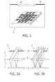
- FIG. 1schematically shows a prior art light sensor with an array of wavelength selective photo-detectors
- FIG. 2schematically shows an embodiment of a light sensor according to the invention
- FIG. 3schematically shows another embodiment of a light sensor according to the invention
- FIG. 4schematically shows a third embodiment of a light sensor according to the invention
- FIG. 5schematically shows a fourth embodiment of a light sensor according to the invention
- FIG. 6schemetically shows two embodiments of an aperture useable in a light sensor according to the invention.
- FIG. 7illustrates an embodiment of a light sensor according to the invention
- FIG. 1schematically shows a light sensor 1 with an array of wavelength selective photo-detectors 10 .
- the light sensorfurther more comprises a lens 20 for projecting the light onto the photo-detectors 10 , and an aperture 30 for defining the field of view of the sensor.
- the light sensor 1further comprises appropriate electronics and a user interface (not shown) for further processing and presentation of the detected light to a user.
- the wavelength selective photo-detectors 10may be made of a diode or charge coupled device covered by an interference filter or Fabry-Perot etalon.
- the varying transmission function (i.e. the wavelength selectivity) of these filtersis caused by interference between the multiple reflections of light between two (or more) reflecting surfaces. Constructive interference occurs if the transmitted beams are in phase. This corresponds to a high-transmission peak of the filter. If the transmitted beams are out-of-phase destructive interference occurs, corresponding to a transmission minimum.
- the multiply-reflected beamsare in-phase or not depends on the wavelength ( ⁇ ) of the light, the angle ( ⁇ ) the light travels through the filter, the thickness (t) of the filter(layers) and the refractive index (n) of the material between the reflecting surfaces.
- Maximum transmissionoccurs when the optical path length difference (2nt cos ⁇ ) between each transmitted beam is an integer multiple of ⁇ .
- the wavelength range over which a filter transmitscan be made quite selective through control of its finesse. This allows the design of an array of photo-detectors 10 having a multitude of filters with different (layer)thicknesses. Such an array enables an accurate measurement of light spectrum falling on the sensor.
- the transmission relation aboveclearly shows that the peak transmission wavelength shifts to the blue for increasing angle of incidence of the light. Hence, such a light sensor 1 will measure and determine different spectral ranges for light falling on the sensor at non-normal angles.
- the wavelength selective photo-detector 10 , the lens 20 , and the aperture 30are arranged in a telecentric configuration.
- both the photo-detector 10 and the aperture 30are positioned at a distance from the lens 20 equal to its focal length f (see FIGS. 2A&B ).
- Positioning the aperture 30 in the focal plane of the lens 20results in light rays refracted towards the optical axis 21 of the lens 20 .
- Positioning the photo-detector 10 in the focal plane of the lens 20results in light rays focussed on the photo-detector.
- the size of the aperture 30determines the width of the cone. Since the spectral response of the wavelength selective photo-detector 10 depends on the cone width, adjustment of the aperture width or size allows controlling the spectral sensitivity of the sensor 1 .
- varying the aperture 30 width/sizeallows making a trade-off between the (intensity) sensitivity of the sensor and the spectral resolution.
- Varying not only the size of the aperture 30 but also the position of the aperture in the focal plane of the lens 20allows an even larger control of the spectral response of the light sensor 1 .
- the ring diameter 40sets the average angle (defining the peak transmission wavelength of the light sensor 1 ) with which the light impinges on the wavelength selective photo-detector 10
- the ring width 50sets the width of the angular distribution (defining the width of the spectral response of the light sensor 1 ) with which the light impinges.
- scanning the ring diameter 40equates to making a spectral scan over a predetermined wavelength range.
- an electro-optical light modulator 18constitutes such a dynamic and controllable aperture system.
- the electro-optical modulator 18could be a liquid crystal cell, an electro-wetting cell, an in-plane electrophoresis cell moving ink particles in the focal plane under the influence of a control voltage, or even a mechanically operated aperture.
- FIGS. 3A&Bshow, (i) the position of the aperture 30 in a plane perpendicular to the optical axis 21 of lens 20 directly relates to the average angle with which the light impinges on the array of wavelength selective photo-detectors 10 and (ii) the position of the photo-detector 10 in the array directly relates to the direction of light incident on the aperture 30 .
- repositioning or scanning the aperture in/through the focal plane of the lens 20allows determining both spectral and angular information of the light falling on the light sensor 1 .
- FIG. 4schematically shows in a further embodiment a light sensor 100 essentially comprising an array of light sensors 1 according to the invention.
- the light sensor 100comprises an array of wavelength selective photo-detectors 110 , an array of lenses 120 and an array of apertures 130 , where these three arrays are arranged in a telecentric configuration.
- Arranging the array of wavelength dependent photo-detectors 110 in sub-arrays 111 , 112 , 113allows assigning the sub-arrays to a single lens and a single aperture.
- the sub-arrayscomprise photo-detectors all having the same spectral response.
- sub-array 111comprises wavelength selective photo-detectors 11 having a response mainly in the red part of the visible spectrum.
- photo-detectors 12 in sub-array 112have their spectral response mainly in the green part
- the photo-detectors 13 in sub-array 113have theirs in the blue part of the visible spectrum.
- the light sensor 200 shown in FIG. 5comprises an array of wavelength selective photo-detectors 210 , a lens 220 and an aperture 230 , again arranged in a telecentric configuration.
- the array of photo-detectors 210is arranged in sub-arrays 211 , 212 , 213 each comprising wavelength selective photo-detectors 11 , 12 , 13 having their main spectral response in different parts of the visible spectrum.
- the wavelength selective photo-detectors 11 , 12 , 13 in each sub-array 211 , 212 , 213may, for instance, be arranged in a Bayer pattern (i.e. one ‘red’, one ‘blue’, two ‘green’ pixels).
- this embodimentallows interpolating the signals from the various colour filters to obtain full resolution angular and spectral information.
- This embodimenthas the main advantage that only one lens and aperture are needed.
- the size of the variable aperturecontrols the angle of incidence (or more precisely the width of the angular distribution) of the light on photo-detector 10 , and hence the width of the spectral response can be tuned. Consequently, in controlling the aperture size a trade-off is made: a large aperture provides a lot of light, but also a wide angular and hence wide spectral distribution, while a small aperture gives low transmission (and thus noise), but good resolution. Effectively, the resulting power distribution on the photo-detector plane is a convolution of the spectral power distribution and the aperture shape. In an embodiment, instead of a single (uncoded) the aperture 30 ( FIG.
- the light sensor 1comprises a coded ring shaped aperture ( FIG. 6B ).
- the fourier transform of the coded aperture(spatial frequency response of the aperture) is changed in a favorable way, such that de-convolution of the spectrum becomes much easier: a convolution in real space is most easily calculated in frequency / fourier space, since a convolution in real space is a simple multiplication in fourier space.
- the fourier transform of a 1-dimentional block shaped slit transmission function and a 2-dimentional circular apertureis the sinc function and Airy function, respectively.
- the measured spectrumis a convolution of the real spectrum with the transmission function of the slit or aperture.
- the light sensorcomprises a signal processing unit 70 (see FIG. 7 ) that performs this de-convolution.
- the coded ring shape apertureincreases the transmission and hence the sensitivity of light sensor 1 without decreasing the spectral resolution or increasing its size.
Landscapes
- Physics & Mathematics (AREA)
- Spectroscopy & Molecular Physics (AREA)
- General Physics & Mathematics (AREA)
- Optics & Photonics (AREA)
- Spectrometry And Color Measurement (AREA)
- Photometry And Measurement Of Optical Pulse Characteristics (AREA)
Abstract
Description
Claims (15)
Applications Claiming Priority (4)
| Application Number | Priority Date | Filing Date | Title |
|---|---|---|---|
| EP08153115.4 | 2008-03-20 | ||
| EP08153115 | 2008-03-20 | ||
| EP08153115 | 2008-03-20 | ||
| PCT/IB2009/051013WO2009115945A1 (en) | 2008-03-20 | 2009-03-11 | Photo-detector and method of measuring light |
Publications (2)
| Publication Number | Publication Date |
|---|---|
| US20110007306A1 US20110007306A1 (en) | 2011-01-13 |
| US8400627B2true US8400627B2 (en) | 2013-03-19 |
Family
ID=40639561
Family Applications (1)
| Application Number | Title | Priority Date | Filing Date |
|---|---|---|---|
| US12/922,721Expired - Fee RelatedUS8400627B2 (en) | 2008-03-20 | 2009-03-11 | Photo-detector and method of measuring light |
Country Status (7)
| Country | Link |
|---|---|
| US (1) | US8400627B2 (en) |
| EP (1) | EP2260276B1 (en) |
| JP (1) | JP5657517B2 (en) |
| KR (1) | KR101649579B1 (en) |
| CN (1) | CN101978247B (en) |
| TW (1) | TW200946882A (en) |
| WO (1) | WO2009115945A1 (en) |
Cited By (3)
| Publication number | Priority date | Publication date | Assignee | Title |
|---|---|---|---|---|
| US20160118509A1 (en)* | 2014-10-28 | 2016-04-28 | Silicon Laboratories Inc. | Light Detector Using an On-Die Interference Filter |
| US9627424B2 (en) | 2014-11-19 | 2017-04-18 | Silicon Laboratories Inc. | Photodiodes for ambient light sensing and proximity sensing |
| US11175010B2 (en) | 2018-09-20 | 2021-11-16 | Samsung Electronics Co., Ltd. | Illumination device and electronic apparatus including the same |
Families Citing this family (16)
| Publication number | Priority date | Publication date | Assignee | Title |
|---|---|---|---|---|
| CN101964866B (en)* | 2009-07-24 | 2013-03-20 | 鸿富锦精密工业(深圳)有限公司 | Computation and image pickup type digital camera |
| JP5734776B2 (en)* | 2011-07-15 | 2015-06-17 | 株式会社東芝 | The camera module |
| JP5937799B2 (en)* | 2011-09-28 | 2016-06-22 | 株式会社トプコン | Spectral image acquisition device |
| WO2013047627A1 (en) | 2011-09-28 | 2013-04-04 | 株式会社 トプコン | Image acquisition device |
| JP5786672B2 (en)* | 2011-11-18 | 2015-09-30 | セイコーエプソン株式会社 | Spectrometer |
| US9568362B2 (en)* | 2012-12-19 | 2017-02-14 | Viavi Solutions Inc. | Spectroscopic assembly and method |
| CN103162828B (en)* | 2013-02-26 | 2015-10-21 | 浙江大学 | Based on the ultrahigh resolution spectrometer of tunable enamel Pohle-perot filter and array type detector spectrometer |
| US20150090909A1 (en)* | 2013-09-30 | 2015-04-02 | Capella Microsystems (Taiwan), Inc. | Selectable view angle optical sensor |
| JP6161522B2 (en)* | 2013-11-20 | 2017-07-12 | オリンパス株式会社 | Image sensor |
| CN105302286B (en)* | 2014-06-04 | 2020-03-03 | 昇佳电子股份有限公司 | Light sensing device and method for arranging light sensing assembly |
| WO2016203573A1 (en)* | 2015-06-17 | 2016-12-22 | 日立マクセル株式会社 | Image capture device |
| JP7200936B2 (en)* | 2017-06-15 | 2023-01-10 | コニカミノルタ株式会社 | Measuring optics, luminance and colorimeters |
| JP6636663B2 (en)* | 2019-02-28 | 2020-01-29 | マクセル株式会社 | Imaging device and image generation method |
| JP6947891B2 (en)* | 2019-12-18 | 2021-10-13 | マクセル株式会社 | Mobile information terminal |
| US11549847B2 (en)* | 2020-08-19 | 2023-01-10 | Richard Fauconier | Method for restricting laser beams entering an aperture to a chosen dyad and measuring their separation |
| WO2025051513A1 (en)* | 2023-09-05 | 2025-03-13 | Ams-Osram Ag | Optical system, multispectral optical sensor and electric device |
Citations (13)
| Publication number | Priority date | Publication date | Assignee | Title |
|---|---|---|---|---|
| EP0132342A2 (en) | 1983-07-22 | 1985-01-30 | Crosfield Electronics Limited | Controlling light beam spectrum |
| US4783593A (en)* | 1985-12-26 | 1988-11-08 | General Electric Company | Optical system for wide angle IR imager |
| EP0355219A1 (en) | 1988-08-16 | 1990-02-28 | Itek Graphix Corp. | Optical system for stagger compensation in an optical scanner |
| US5258618A (en) | 1991-12-12 | 1993-11-02 | General Electric Company | Infrared imager forming two narrow waveband images of the same object field |
| US5281797A (en)* | 1991-12-26 | 1994-01-25 | Hitachi, Ltd. | Short wavelength optical disk head having a changeable aperture |
| EP1494047A1 (en) | 2003-07-02 | 2005-01-05 | Berner Fachhochschule Hochsschule für Technik und Architektur Biel-Bienne | Aperture for coded-aperture imaging |
| US20050052649A1 (en) | 2003-08-19 | 2005-03-10 | Fuji Photo Film Co., Ltd. | Spectral image measurement apparatus and method using the same |
| US6911637B1 (en) | 2002-05-23 | 2005-06-28 | The United States Of America As Represented By The Secretary Of The Army | Wavefront phase sensors using optically or electrically controlled phase spatial light modulators |
| US20050260741A1 (en)* | 2004-05-20 | 2005-11-24 | The Regents Of The University Of California | Wide field image for quantitative analysis of microarrays |
| US7095009B2 (en) | 2002-05-21 | 2006-08-22 | 3M Innovative Properties Company | Photopic detector system and filter therefor |
| US20070081158A1 (en) | 2005-01-19 | 2007-04-12 | David Brady | Static two-dimensional aperture coding for multimodal multiplex spectroscopy |
| US7280205B2 (en) | 2005-03-02 | 2007-10-09 | Li-Cor, Inc. | On-chip spectral filtering using CCD array for imaging and spectroscopy |
| US7292341B2 (en) | 2002-05-09 | 2007-11-06 | Nova Measuring Instruments Ltd. | Optical system operating with variable angle of incidence |
Family Cites Families (8)
| Publication number | Priority date | Publication date | Assignee | Title |
|---|---|---|---|---|
| US3278752A (en)* | 1963-06-17 | 1966-10-11 | Berlyn B Brixner | Wide angle optical system having a telecentric stop and an interference filter |
| JPH04113235A (en)* | 1990-09-04 | 1992-04-14 | Minolta Camera Co Ltd | Photosensor |
| JPH07226825A (en)* | 1994-02-15 | 1995-08-22 | Fuji Xerox Co Ltd | Color image reader |
| JP4454098B2 (en)* | 2000-03-21 | 2010-04-21 | 株式会社トプコン | Photometric device |
| JP2001296180A (en)* | 2000-04-12 | 2001-10-26 | Mitsubishi Electric Corp | Spectral image acquisition device |
| JP2004279140A (en)* | 2003-03-13 | 2004-10-07 | Omron Corp | Plasma spectrophotometer |
| US7283232B2 (en)* | 2005-06-06 | 2007-10-16 | Duke University | Optical spectroscopy with overlapping images |
| US7286232B2 (en)* | 2006-02-15 | 2007-10-23 | Li-Cor, Inc. | Fluorescence filtering system and method for molecular imaging |
- 2009
- 2009-03-11USUS12/922,721patent/US8400627B2/ennot_activeExpired - Fee Related
- 2009-03-11EPEP09723266.4Apatent/EP2260276B1/ennot_activeNot-in-force
- 2009-03-11KRKR1020107023463Apatent/KR101649579B1/ennot_activeExpired - Fee Related
- 2009-03-11CNCN2009801099543Apatent/CN101978247B/ennot_activeExpired - Fee Related
- 2009-03-11WOPCT/IB2009/051013patent/WO2009115945A1/enactiveApplication Filing
- 2009-03-11JPJP2011500319Apatent/JP5657517B2/ennot_activeExpired - Fee Related
- 2009-03-19TWTW098108961Apatent/TW200946882A/enunknown
Patent Citations (14)
| Publication number | Priority date | Publication date | Assignee | Title |
|---|---|---|---|---|
| EP0132342A2 (en) | 1983-07-22 | 1985-01-30 | Crosfield Electronics Limited | Controlling light beam spectrum |
| US4783593A (en)* | 1985-12-26 | 1988-11-08 | General Electric Company | Optical system for wide angle IR imager |
| EP0355219A1 (en) | 1988-08-16 | 1990-02-28 | Itek Graphix Corp. | Optical system for stagger compensation in an optical scanner |
| US5258618A (en) | 1991-12-12 | 1993-11-02 | General Electric Company | Infrared imager forming two narrow waveband images of the same object field |
| US5281797A (en)* | 1991-12-26 | 1994-01-25 | Hitachi, Ltd. | Short wavelength optical disk head having a changeable aperture |
| US7292341B2 (en) | 2002-05-09 | 2007-11-06 | Nova Measuring Instruments Ltd. | Optical system operating with variable angle of incidence |
| US7095009B2 (en) | 2002-05-21 | 2006-08-22 | 3M Innovative Properties Company | Photopic detector system and filter therefor |
| US6911637B1 (en) | 2002-05-23 | 2005-06-28 | The United States Of America As Represented By The Secretary Of The Army | Wavefront phase sensors using optically or electrically controlled phase spatial light modulators |
| EP1494047A1 (en) | 2003-07-02 | 2005-01-05 | Berner Fachhochschule Hochsschule für Technik und Architektur Biel-Bienne | Aperture for coded-aperture imaging |
| US20050052649A1 (en) | 2003-08-19 | 2005-03-10 | Fuji Photo Film Co., Ltd. | Spectral image measurement apparatus and method using the same |
| US20050260741A1 (en)* | 2004-05-20 | 2005-11-24 | The Regents Of The University Of California | Wide field image for quantitative analysis of microarrays |
| US20070081158A1 (en) | 2005-01-19 | 2007-04-12 | David Brady | Static two-dimensional aperture coding for multimodal multiplex spectroscopy |
| US20080106732A1 (en) | 2005-01-19 | 2008-05-08 | Duke University | Static two-dimensional aperture coding for multimodal multiplex spectroscopy |
| US7280205B2 (en) | 2005-03-02 | 2007-10-09 | Li-Cor, Inc. | On-chip spectral filtering using CCD array for imaging and spectroscopy |
Non-Patent Citations (2)
| Title |
|---|
| Veeraraghavan et al: "Non-Refractive Modulators for Encoding and Capturing Scene Appearance and Depth"; IEEE Conference on Computer Vision and Pattern Recognition, CVPR 2008, pp. 1-8. |
| Zomet et al: "Lensless Imaging With a Controllable Aperture"; Proceedings of the 2006 IEEE Computer Society Conference on Computer Vision and Pattern Recognition 2006 (CVPR'06), 8 Page Document. |
Cited By (6)
| Publication number | Priority date | Publication date | Assignee | Title |
|---|---|---|---|---|
| US20160118509A1 (en)* | 2014-10-28 | 2016-04-28 | Silicon Laboratories Inc. | Light Detector Using an On-Die Interference Filter |
| US9978887B2 (en)* | 2014-10-28 | 2018-05-22 | Silicon Laboratories Inc. | Light detector using an on-die interference filter |
| US9627424B2 (en) | 2014-11-19 | 2017-04-18 | Silicon Laboratories Inc. | Photodiodes for ambient light sensing and proximity sensing |
| US11175010B2 (en) | 2018-09-20 | 2021-11-16 | Samsung Electronics Co., Ltd. | Illumination device and electronic apparatus including the same |
| US11441755B2 (en) | 2018-09-20 | 2022-09-13 | Samsung Electronics Co., Ltd. | Illumination device and electronic apparatus including the same |
| US12104894B2 (en) | 2018-09-20 | 2024-10-01 | Samsung Electronics Co., Ltd. | Illumination device and electronic apparatus including the same |
Also Published As
| Publication number | Publication date |
|---|---|
| CN101978247A (en) | 2011-02-16 |
| JP2011515675A (en) | 2011-05-19 |
| CN101978247B (en) | 2012-03-21 |
| KR20100125434A (en) | 2010-11-30 |
| EP2260276B1 (en) | 2018-05-16 |
| EP2260276A1 (en) | 2010-12-15 |
| TW200946882A (en) | 2009-11-16 |
| KR101649579B1 (en) | 2016-08-19 |
| JP5657517B2 (en) | 2015-01-21 |
| WO2009115945A1 (en) | 2009-09-24 |
| US20110007306A1 (en) | 2011-01-13 |
Similar Documents
| Publication | Publication Date | Title |
|---|---|---|
| US8400627B2 (en) | Photo-detector and method of measuring light | |
| KR102780276B1 (en) | Spectrometer on a chip | |
| JP7154230B2 (en) | Optical Imaging Transmitter with Enhanced Brightness | |
| CN112985603B (en) | Reference switch architecture for non-contact sensing of substances | |
| US20180188110A1 (en) | Fabry-perot spectrometer apparatus and methods | |
| US9417132B2 (en) | Multispectral imaging color measurement system and method for processing imaging signals thereof | |
| US9307127B2 (en) | Image capturing device and image capturing system | |
| JP5694339B2 (en) | Spectral detection device for detecting spectral components of received light | |
| JPH10185688A (en) | Fabry-Perot spectrometer for detecting the spectral signature of a distributed light source that changes in space | |
| JPH04213403A (en) | Variable wavelength optical filter and sensor system | |
| CA2330311A1 (en) | Corrected concentric spectrometer | |
| EP2473826A1 (en) | High spectral resolution color sensor using non-dispersive elements | |
| JP2014095688A (en) | Imaging device and imaging system | |
| CN114599946B (en) | Spectrometers and imaging devices | |
| WO2020239481A1 (en) | Spectral reconstruction with multi-channel color sensors | |
| KR20120120174A (en) | Microarray-based spatial filter | |
| US5914777A (en) | Apparatus for and method of measuring a distribution of luminous intensity of light source | |
| US10139339B2 (en) | Colour sensor with angle-selective structures | |
| JP2003114107A (en) | Film thickness measuring device | |
| US12271004B2 (en) | Imager and spot sampler with translatable stage | |
| US20240063240A1 (en) | Light state imaging pixel | |
| US11454708B2 (en) | Lidar device | |
| JP6331986B2 (en) | Optical property measuring device | |
| US20210172802A1 (en) | Optical device allowing the angular and spectral emission of an object to be measured simultaneously | |
| JPH05231931A (en) | Illuminance measurement receiver and radiance meter |
Legal Events
| Date | Code | Title | Description |
|---|---|---|---|
| AS | Assignment | Owner name:KONINKLIJKE PHILIPS ELECTRONICS N V, NETHERLANDS Free format text:ASSIGNMENT OF ASSIGNORS INTEREST;ASSIGNORS:JAK, MARTIN JACOBUS JOHAN;VAN DEN BIGGELAAR, THEODORUS JOHANNES PETRUS;MEIJER, EDUARD JOHANNES;AND OTHERS;REEL/FRAME:024989/0782 Effective date:20090312 | |
| STCF | Information on status: patent grant | Free format text:PATENTED CASE | |
| AS | Assignment | Owner name:KONINKLIJKE PHILIPS N.V., NETHERLANDS Free format text:CHANGE OF NAME;ASSIGNOR:KONINKLIJKE PHILIPS ELECTRONICS N.V.;REEL/FRAME:039428/0606 Effective date:20130515 | |
| FPAY | Fee payment | Year of fee payment:4 | |
| AS | Assignment | Owner name:PHILIPS LIGHTING HOLDING B.V., NETHERLANDS Free format text:ASSIGNMENT OF ASSIGNORS INTEREST;ASSIGNOR:KONINKLIJKE PHILIPS N.V.;REEL/FRAME:040060/0009 Effective date:20160607 | |
| FEPP | Fee payment procedure | Free format text:MAINTENANCE FEE REMINDER MAILED (ORIGINAL EVENT CODE: REM.); ENTITY STATUS OF PATENT OWNER: LARGE ENTITY | |
| LAPS | Lapse for failure to pay maintenance fees | Free format text:PATENT EXPIRED FOR FAILURE TO PAY MAINTENANCE FEES (ORIGINAL EVENT CODE: EXP.); ENTITY STATUS OF PATENT OWNER: LARGE ENTITY | |
| STCH | Information on status: patent discontinuation | Free format text:PATENT EXPIRED DUE TO NONPAYMENT OF MAINTENANCE FEES UNDER 37 CFR 1.362 | |
| FP | Lapsed due to failure to pay maintenance fee | Effective date:20210319 |