US8400555B1 - Focused plenoptic camera employing microlenses with different focal lengths - Google Patents
Focused plenoptic camera employing microlenses with different focal lengthsDownload PDFInfo
- Publication number
- US8400555B1 US8400555B1US12/628,437US62843709AUS8400555B1US 8400555 B1US8400555 B1US 8400555B1US 62843709 AUS62843709 AUS 62843709AUS 8400555 B1US8400555 B1US 8400555B1
- Authority
- US
- United States
- Prior art keywords
- microlenses
- camera
- microlens
- array
- different
- Prior art date
- Legal status (The legal status is an assumption and is not a legal conclusion. Google has not performed a legal analysis and makes no representation as to the accuracy of the status listed.)
- Expired - Fee Related, expires
Links
Images


Classifications
- H—ELECTRICITY
- H04—ELECTRIC COMMUNICATION TECHNIQUE
- H04N—PICTORIAL COMMUNICATION, e.g. TELEVISION
- H04N23/00—Cameras or camera modules comprising electronic image sensors; Control thereof
- H04N23/95—Computational photography systems, e.g. light-field imaging systems
- H04N23/957—Light-field or plenoptic cameras or camera modules
- H—ELECTRICITY
- H04—ELECTRIC COMMUNICATION TECHNIQUE
- H04N—PICTORIAL COMMUNICATION, e.g. TELEVISION
- H04N23/00—Cameras or camera modules comprising electronic image sensors; Control thereof
- H04N23/60—Control of cameras or camera modules
- H04N23/67—Focus control based on electronic image sensor signals
- H04N23/676—Bracketing for image capture at varying focusing conditions
Definitions
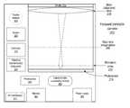
- FIG. 1illustrates imaging in a conventional camera.
- “Inside world”represents inside the camera.
- the shaded oval regionsrepresent the order of depths in the outside world, and the corresponding depths inside the camera.
- One particular image plane inside the camerais shown.
- the mapping of the 3D world of the scene outside camera into a 3D world inside camerais governed by the lens equation:
- a and Bare respectively the distances from the lens to the object plane and from the lens to the image plane.
- a and Bare respectively the distances from the lens to the object plane and from the lens to the image plane.
- This equationis normally used to describe the effect of a single image mapping between two fixed planes. In reality, however, the lens equation describes an infinite number of mappings—it constrains the relationship between, but does not fix, the values of the distances A and B. That is, every plane in the outside scene (which is described as being at some distance A from the objective lens) is mapped by the objective lens to a corresponding plane inside of the camera at a distance B.
- a sensore.g., conventional film, a charge-coupled device (CCD), etc.
- CCDcharge-coupled device
- Conventional camerasrender a three-dimensional scene onto a two-dimensional sensor.
- a conventional digital cameracaptures a two-dimensional (2-D) image representing a total amount of light that strikes each point on a photosensor within the camera.
- this 2-D imagecontains no information about the direction of the light that strikes the photosensor.
- the image captured by a conventional cameraessentially integrates the radiance function over its angular portion, resulting in a two-dimensional intensity as a function of position. The angular information of the original radiance is lost.
- conventional camerasfail to capture a large amount of optical information.
- light-field, or radiance capturingcameras sample the four-dimensional (4-D) optical phase space or light-field, and in doing so capture information about the directional distribution of the light rays.
- This information captured by light-field camerasmay be referred to as the light-field, the plenoptic function, or radiance.
- a light-fieldis a 4-D record of all light rays in 3-D.
- Radiancedescribes both spatial and angular information, and is defined as density of energy per unit of area per unit of stereo angle (in radians).
- a light-field cameracaptures radiance; therefore, light-field images originally taken out-of-focus may be refocused, noise may be reduced, viewpoints may be changed, and other light-field effects may be achieved.
- Light-fieldsmay be captured with a conventional camera.
- M ⁇ N images of a scenemay be captured from different positions with a conventional camera. If, for example, 8 ⁇ 8 images are captured from 64 different positions, 64 images are produced. The pixel from each position (i, j) in each image are taken and placed into blocks, to generate 64 blocks.
- FIG. 2illustrates an example prior art light-field camera, or camera array, which employs an array of two or more objective lenses 110 . Each objective lens focuses on a particular region of photosensor 108 , or alternatively on a separate photosensor 108 .
- This light-field camera 100may be viewed as a combination of two or more conventional cameras that each simultaneously records an image of a subject on a particular region of photosensor 108 or alternatively on a particular photosensor 108 . The captured images may then be combined to form one image.
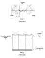
- FIG. 3illustrates an example prior art plenoptic camera, another type of radiance capturing camera, that employs a single objective lens and a microlens or lenslet array 106 that includes, for example, about 100,000 lenslets.
- lenslet array 106is fixed at a small distance ( ⁇ 0.5 mm) from a photosensor 108 , e.g. a charge-coupled device (CCD).
- CCDcharge-coupled device
- the microlensesare placed and adjusted accurately to be exactly at one focal length f from the sensor 108 . This is done by placing the array of microlenses at distance f from the sensor, where f is the focal length of the microlenses.
- the raw image captured with plenoptic camera 102is made up of an array of small images, typically circular, of the main lens 108 . These small images may be referred to as microimages.
- each microlensdoes not create an image of the internal world on the sensor 108 , but instead creates an image of the main camera lens 104 .
- the lenslet array 106enables the plenoptic camera 102 to capture the light-field, i.e. to record not only image intensity, but also the distribution of intensity in different directions at each point.
- Each lensletsplits a beam coming to it from the main lens 104 into rays coming from different locations on the aperture of the main lens 108 .
- Each of these raysis recorded as a pixel on photosensor 108 , and the pixels under each lenslet collectively form an n-pixel image.
- This n-pixel area under each lensletmay be referred to as a macropixel, and the camera 102 generates a microimage at each macropixel.
- the plenoptic photograph captured by a camera 102 with, for example, 100,000 lensletswill contain 100,000 macropixels, and thus generate 100,000 microimages of a subject.
- Each macropixelcontains different angular samples of the light rays coming to a given microlens.
- Each macropixelcontributes to only one pixel in the different angular views of the scene; that is, only one pixel from a macropixel is used in a given angular view.
- each angular viewcontains 100,000 pixels, each pixel contributed from a different macropixel.
- Another type of integral or light-field camerais similar to the plenoptic camera of FIG. 3 , except that an array of pinholes is used between the main lens and the photosensor instead of an array of lenslets.
- FIG. 4further illustrates an example prior art plenoptic camera model.
- conventional plenoptic camera 102the microlens-space system swaps positional and angular coordinates of the radiance at the microlens. For clarity, only the rays through one of the microlenses are illustrated.
- the conventional optical analysis of such a plenoptic cameraconsiders it as a cascade of a main lens system followed by a microlens system. The basic operation of the cascade system is as follows. Rays focused by the main lens 104 are separated by the microlenses 106 and captured on the sensor 108 . At their point of intersection, the rays have the same position but different slopes.
- each microlensfunctions to swap the positional and angular coordinates of the radiance, then this new positional information is captured by the sensor 108 . Because of the swap, it represents the angular information at the microlens. As a result, each microlens image captured by sensor 108 represents the angular information for the radiance at the position of the optical axis of the corresponding microlens.
- the light-fieldis the radiance density function describing the flow of energy along all rays in three-dimensional (3D) space. Since the description of a ray's position and orientation requires four parameters (e.g., two-dimensional positional information and two-dimensional angular information), the radiance is a four-dimensional (4D) function. This function may be referred to as the plenoptic function.
- Image sensor technologyon the other hand, is only two-dimensional, and light-field imagery must therefore be captured and represented in flat (two dimensional) form.
- a variety of techniqueshave been developed to transform and capture the 4D radiance in a manner compatible with 2D sensor technology. This may be referred to as a flat representation of the 4D radiance (or light-field), or simply as a flat.
- Focus bracketinginvolves taking multiple images without moving the camera while focusing at different depths. The images may then be appropriately combined to generate an image that is in-focus at different depths (e.g., foreground and background). Focus bracketing is thus a conventional technique for increasing depth of field. Some conventional cameras have an automatic setting to capture three or more images while changing the focus in a rapid sequence, thus achieving automatic focus bracketing. However, focus bracketing and other similar conventional techniques cannot compensate for the fact that the images are consecutive in time, and if the field of view being captured is changing, the images do not represent the same scene.
- Conventional plenoptic camerasmay provide the ability to focus and refocus images from a single flat after the flat is captured.
- conventional plenoptic camerasrequire extremely high pixel count for the captured image in order to create quality refocused images.
- Embodimentsmay leverage the characteristics of a focused plenoptic camera as described herein to produce quality output images that are in-focus at different depths. Considering the fact that the focused plenoptic camera simultaneously captures multiple, almost identical, microimages, embodiments of a focused plenoptic camera that include microlenses with at least two different focal lengths may be used to simultaneously capture microimages from at least two different planes at different distances from the microlens array.
- a focused plenoptic camera that includes microlenses with two different focal lengthsmay capture some of the microimages from one plane at a distance a from the microlens array, and capture others of the microimages from another plane at a different distance a′ from the microlens array.
- a focused plenoptic camera that includes microlenses with n different focal lengthsmay be considered as essentially the equivalent of n focused plenoptic cameras in one.
- Each of these n “cameras”has some amount of 3D capability, but each “camera” is focused at a different depth. Image operations such as refocusing and focus bracketing are thus made possible from such “multiple camera” data. Since all of the microimages in a flat are captured by the focused plenoptic camera at the same time, there is no problem with dynamic scenes in the field of view as there is when using conventional cameras to perform focus bracketing by capturing a sequence of temporally different images.
- imagesmay be constructed from subsets of the microimages captured using each type of microlens, thus creating n images each focused at a different depth.
- One or more image processing techniquesmay be applied to two or more of these n images to produce a combined image that incorporates in-focus regions of the two or more images.
- Embodimentsare described in which an array of single microlenses including at least two different microlenses with different focal lengths are employed; in these embodiments, each single lens may be considered an optical element.
- Embodimentsare also described in which an array of stacks of two (or potentially more) microlenses including at least two different stacks that provide different focal lengths are employed; in these embodiments, each stack of two (or more) microlenses may be considered an optical element.
- the lens stacksmay be provided by stacking two microlenses arrays on top of each other in the camera.
- one of the two microlens arraysincludes microlenses all of the same focal length, while the other microlens array includes at least two different microlenses of different focal lengths.
- the different microlensesmay also provide different depths of field.
- FIG. 1illustrates imaging in a conventional camera.
- FIG. 2illustrates an example prior art light-field camera, or camera array, which employs an array of two or more objective lenses.
- FIG. 3illustrates an example prior art plenoptic camera that employs a single objective lens and a microlens array.
- FIG. 4further illustrates an example prior art plenoptic camera.
- FIG. 5Ashows a raw light-field image, or flat, as captured by a plenoptic camera.
- FIG. 5Bshows a final image rendered from the flat of FIG. 5A according to a conventional rendering method.
- FIG. 5Cshows a final image rendered from the flat of FIG. 5A according to an embodiment of the full-resolution light-field rendering method.
- FIG. 6is a block diagram illustrating a focused plenoptic camera according to one embodiment.
- FIG. 7illustrates an example embodiment of a focused plenoptic camera with various other elements that may be integrated in the camera.
- FIG. 8illustrates an example embodiment of a focused plenoptic camera based on a large-format film camera.
- FIG. 9shows an example crop from a flat captured with a plenoptic camera.
- FIG. 10illustrates the Keplerian telescopic case for a plenoptic camera.
- FIG. 11shows a crop from the roof area in FIG. 9 , and visually illustrates the Keplerian telescopic behavior in light-field cameras.
- FIG. 12illustrates the Galilean telescopic case for a plenoptic camera.
- FIG. 13shows a crop from the tree area in FIG. 9 , and visually illustrates the Galilean telescopic behavior in light-field cameras.
- FIG. 15illustrates a lens circle (or microimage) of diameter D and a patch or crop of size m 1 ⁇ m 2 , where at least one of m 1 and m 2 is an integer greater than or equal to 2.
- FIG. 16shows a zoom into an example microlens array.
- FIG. 17shows a portion of a digitized flat.
- FIGS. 18A through 18Cshow output images rendered from a flat using conventional rendering methods.
- FIG. 19shows a full-resolution rendering of a light-field, rendered assuming the Keplerian telescopic case according to one embodiment of the full-resolution light-field rendering method.
- FIG. 20shows a full-resolution rendering of a light-field, rendered assuming the Galilean telescopic case according to one embodiment of the full-resolution light-field rendering method.
- FIG. 21is a flow chart illustrating how light is directed within a focused plenoptic camera according to one embodiment.
- FIG. 22is a flowchart of a full-resolution light-field rendering method according to one embodiment.
- FIG. 23illustrates a rendering module rendering a high-resolution image from a flat captured, for example, by a focused plenoptic camera, according to some embodiments.
- FIG. 24illustrates an example computer system that may be used in embodiments.
- FIG. 25is a flowchart of a full-resolution light-field rendering method in which multiple images are rendered from a flat and combined to produce a final high-resolution output image, according to some embodiments.
- FIG. 26shows an example full-resolution rendering of a light-field in which foreground and background portions of the images shown in FIGS. 19 and 20 have been combined, according to one embodiment of the full-resolution light-field rendering method.
- FIGS. 27A and 27Billustrate the different modes or configurations of a focused plenoptic camera according to some embodiments.
- FIG. 28is a block diagram illustrating a focused plenoptic camera including different microlenses with different focal lengths and depths of focus, according to some embodiments.
- FIG. 29illustrates a portion of a microlens array including and alternating pattern of microlenses of two different focal lengths, according to some embodiments.
- FIG. 30shows a portion of an example microlens array including an alternating pattern of microlenses of four different focal lengths, according to some embodiments.
- FIG. 31is a block diagram illustrating a focused plenoptic camera including stacks of two or more microlenses in a microlens array with different focal lengths provided by different microlens stacks, according to some embodiments.
- FIG. 32illustrates a portion of an example array including an alternating pattern of microlens stacks that provide different focal lengths, according to some embodiments.
- FIG. 33illustrates portions of two example microlens arrays that may be combined to form an array of microlens stacks, according to some embodiments.
- FIG. 34Ashows two example microlens arrays with the microlenses facing each other, according to some embodiments.
- FIG. 34Billustrates an arrangement in which the microlenses in the microlens array with microlenses of different focal lengths are facing the flat side of the microlens array including microlenses all of the same focal length, according to some embodiments.
- FIG. 35is an optical representation of the arrangement shown in FIG. 34A .
- FIG. 36is an optical representation of the arrangement shown in FIG. 34B .
- FIG. 37shows the arrangement of FIG. 34B in which the main microlens array is positioned one focal lengths from the photosensor, according to some embodiments.
- FIG. 38is a block diagram illustrating an example embodiment of a focused plenoptic camera that includes an array of optical elements in which different ones of the optical elements provide different focal lengths.
- FIG. 39shows an example microlens array that may be used as a second microlens array in a stack of microlens arrays and that includes four different microlenses with different focal lengths arranged in a checkerboard pattern, according to some embodiments.
- FIG. 40graphically illustrates a portion of a flat including circular microimages that may be captured using a microlens array similar to the example microlens array shown in FIG. 39 .
- FIG. 41graphically illustrates a portion of a flat including rectangular microimages that may be captured using a microlens array similar to the example microlens array shown in FIG. 39 .
- FIG. 42is a block diagram illustrating a focused plenoptic camera, for example as illustrated in FIG. 6 , including an array of optical elements that provides two or more different focal lengths, according to some embodiments.
- FIG. 43is a flowchart illustrating how light is directed within a focused plenoptic camera including an array of optical elements that provides two or more different focal lengths, according to some embodiments.
- FIG. 44is a flowchart illustrating a method in which microimages captured at different focal lengths are first combined to produce two or more separate images, according to some embodiments.
- FIG. 45graphically illustrates a method in which microimages captured at different focal lengths are first combined to produce two or more separate images, according to some embodiments.
- FIG. 46illustrates an example optical element array that includes microlens arrays on both sides of a wafer, according to some embodiments.
- FIGS. 47A and 47Billustrate an example optical element array that includes three stacked microlens arrays according to some embodiments.
- FIGS. 48A through 48Dillustrate several example modes or configurations of a focused plenoptic camera employing microlenses with different focal lengths, according to various embodiments.
- such quantitiesmay take the form of electrical or magnetic signals capable of being stored, transferred, combined, compared or otherwise manipulated. It has proven convenient at times, principally for reasons of common usage, to refer to such signals as bits, data, values, elements, symbols, characters, terms, numbers, numerals or the like. It should be understood, however, that all of these or similar terms are to be associated with appropriate physical quantities and are merely convenient labels. Unless specifically stated otherwise, as apparent from the following discussion, it is appreciated that throughout this specification discussions utilizing terms such as “processing,” “computing,” “calculating,” “determining” or the like refer to actions or processes of a specific apparatus, such as a special purpose computer or a similar special purpose electronic computing device.
- a special purpose computer or a similar special purpose electronic computing deviceis capable of manipulating or transforming signals, typically represented as physical electronic or magnetic quantities within memories, registers, or other information storage devices, transmission devices, or display devices of the special purpose computer or similar special purpose electronic computing device.
- Embodiments of a full-resolution radiance camerawhich may also be referred to as a radiance camera or a focused plenoptic camera, and of a method for rendering high-resolution images from flat 2D representations of the 4D lightfield, referred to herein as flats, captured by embodiments of the focused plenoptic camera, are described.
- the method for rendering high-resolution images from flats captured by embodiments of the focused plenoptic cameramay be referred to as a full-resolution light-field rendering method, or simply as the light-field rendering method.
- full resolutiondoes not directly refer to sensor resolution of the camera, but instead refers to resolution as supported by the captured radiance data.
- Light-field photographyenables many new possibilities for digital imaging because it captures both spatial and angular information, i.e., the full four-dimensional radiance, of a scene.
- High-resolutionis required in order to capture four-dimensional data with a two-dimensional sensor.
- images rendered from this data as projections of the four-dimensional radiance onto two spatial dimensions using conventional light-field cameras and conventional light-field rendering methodsare at significantly lower resolutions.
- Embodiments of the focused plenoptic camera and of the full-resolution light-field rendering methodmore adequately meet the resolution and image size expectations of modern photography than do conventional light-field cameras and rendering methods.
- the microlenses in the microlens arrayare focused on the image plane of the main camera lens, rather than on the main camera lens itself as in conventional plenoptic cameras.
- the image planethere is a real image of a scene in front of the camera and refracted by the main lens to the image plane, but there is nothing there physically (other than light); the image plane is simply a plane location in space that can be considered to have an image “in the air” as created by the main lens.
- the microlenses, being focused on the image plane instead of on the main lens,can capture the image of the scene at the image plane.
- Each microlenscaptures a small area or region of the image at the image plane and maps or projects the captured region onto a corresponding region of the photosensor.
- the imaging property of the focused plenoptic cameramay be viewed as two steps: from the world through the main lens to the image plane, and then from the image plane through the microlenses to the photosensor. This is similar to a cascade of two cameras, but the second camera is actually many small cameras, as each microlens is effectively a little camera that captures a small image from the image plane. This is also similar to the way a telescope operates.
- embodiments of the focused plenoptic cameraare able to fully capture the positional information of the radiance.
- Embodiments of the full-resolution light-field rendering methodmay be used to render full-resolution images from flats captured by embodiments of the focused plenoptic camera, producing output images at a dramatically higher resolution than conventional light-field rendering techniques.
- Embodimentsmay render images at spatial resolutions that meet the expectations of modern photography (e.g., 10 megapixel and beyond), making light-field photography much more practical.
- embodimentsexploit the fact that, at every plane of depth, the radiance contains a considerable amount of positional information about the scene, encoded in the angular information at that plane. Accordingly, embodiments may be referred to as full-resolution because embodiments make full use of both angular and positional information that is available in the four-dimensional radiance, as shown in the analysis. In contrast to super-resolution techniques, which create high-resolution images from sub-pixel shifted low-resolution images, embodiments render high-resolution images directly from the radiance data. Moreover, embodiments may generate light-field images that are amenable to radiance processing techniques such as Fourier slice refocusing.
- FIGS. 5A through 5Cshow, for comparison, results from a conventional plenoptic camera and rendering method and results from example embodiments of a focused plenoptic camera and full-resolution light-field rendering method as described herein.
- FIG. 5Ashows a raw light-field image as captured by a plenoptic camera. Note that, to the untrained human eye, the raw light-field image captured by a conventional plenoptic camera may look similar to the raw light-field image captured by an embodiment of the focused plenoptic camera.
- FIG. 5Bshows a conventionally rendered final image
- FIG. 5Cshows a final image rendered according to an embodiment of the full-resolution light-field rendering method as described herein. Even in this small, grayscale format, a drastic improvement in spatial resolution in FIG. 5C when compared to the spatial resolution in FIG. 5B is easily observable.
- a focused plenoptic cameraVarious embodiments of a focused plenoptic camera are described.
- the microlensesare placed and adjusted accurately to be exactly at one focal length f from the photosensor, where f is the focal length of the microlenses.
- the microlens arrayis fixed at the image plane of the main or objective lens of the camera, and the microlenses in the array are focused at infinity.
- the microlensesare focused on the image created by the main lens inside the camera and in front of the microlenses (the image plane of the main lens), instead of being focused on the main lens itself, as in conventional plenoptic cameras.
- the microlenses in embodiments of the focused plenoptic camera described hereinmay be located at, or may be moved to, distances greater than for less than f from the photosensor, where f is the focal length of the microlenses.
- the array of microlensesmay be placed at distance 4/3 f from the photosensor. Other embodiments may place the array of microlenses at other distances that are multiples of f e.g. 1.5 f or 3 ⁇ 4 f.
- embodiments of focused plenoptic cameras in which the distance of the microlens array from the photosensor is variable or adjustable, and in which other characteristics of the camera may be adjustableare described.
- the distance of the microlens array from the photosensormay be adjustable within the range 0.5 f to 1.5 f.
- a maximum useful distancemay be 1.5 f, although distances greater than 1.5 f may be possible, if not practical.
- a practical range for the distance of the microlens array from the photosensormay be f ⁇ b ⁇ 1.5 f.
- the photosensoris a digital light-capturing device or medium such as a charge-coupled device (CCD) that captures and records the light in digital format.
- CCDcharge-coupled device
- the photosensoris a film.
- photosensorrefers to digital media that are used in digital cameras to capture light and to film media that are used in film cameras to capture light, and more generally to any device or medium that may be used to capture light.
- Light-field images captured on a film using film camera embodimentsmay subsequently be digitized, for example using a high-resolution scanner, so that the captured light-field may be rendered, for example using the full-resolution light-field rendering method described herein, to produce high-resolution output images.
- Light-field images captured using digital camera embodimentsmay be directly rendered.
- the photosensor and the microlens arrayare at a fixed distance b from each other (the distance b is a multiple of f, for example 4/3 f 3 ⁇ 4 f, or 1.5 f, where f is the focal length of the microlenses).
- bis used herein to designate the distance between the microlenses and the photosensor, while a is used herein to designate the distance between the microlenses and the image plane of the main or objective lens.
- the microlens array/photosensor combinationmay be fixed at a location in the camera body.
- the microlens arraymay be fixed in optical characteristics as well as in its physical location.
- the main lens of the cameramay also be fixed in optical characteristics and location, while possibly allowing for changes in shutter speed, aperture, focusing, etc.
- various manual or automatic mechanismsmay be employed to change the distance b between the photosensor and the microlens array, to change the location of the microlens array/photosensor combination in the camera body, to change the distance from the main lens to the microlens array, to change the distance a between the microlenses and the image plane, and/or to swap or replace various components such as the microlens array and the main lens.
- the main lens of the cameramay be swappable to use different main lenses, and may be adjustable according to aperture, shutter speed, focusing, distance from the microlens array, and so on.
- the microlens arraymay be swappable, so that microlens arrays with different numbers of microlenses and/or microlenses with different optical characteristics may be used, are also possible.
- the optical characteristics of the optical systemis important in capturing light-fields that may be rendered to yield high-resolution output images as described herein.
- the microlenses, main lens, photosensor, and the relative physical location of these components in the cameramay be determined according to the formulas and equations described herein to capture appropriate and satisfactory light-field images.
- some embodimentsmay include automated mechanisms that automatically adjust the positioning or other aspects of one or more of the components to capture appropriate and satisfactory light-field images. For example, if the user adjusts or replaces one component, the camera may automatically adjust one or more other components to compensate for the change.
- a human operator of an adjustable focused plenoptic cameramay manually adjust the positioning or other aspects of one or more of the components, may replace one or more components with units that have different characteristics, or may insert other components (e.g., microsheet glass, as described below) to capture appropriate and satisfactory light-field images.
- other componentse.g., microsheet glass, as described below
- FIGS. 6 through 8illustrate example film camera and digital camera embodiments of a focused plenoptic camera as described herein, and further illustrate both fixed and adjustable embodiments of the focused plenoptic camera. It is noted that these are example embodiments, and are not intended to be limiting. Other embodiments are possible and anticipated.
- FIG. 6is a block diagram illustrating a focused plenoptic camera according to one embodiment.
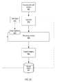
- Focused plenoptic camera 200may include a main (objective) lens 230 , a microlens array 220 , and a photosensor 210 .
- Microlens array 220may be located at a distance greater than f from photosensor 210 , where f is the focal length of the microlenses in array 220 .
- the microlenses in array 220are focused on the image plane 240 of the main lens 230 .
- conventional plenoptic camerassuch as plenoptic camera 102 of FIGS.
- the microlens array 106is fixed at distance f from photosensor 108 , and the microlenses in array 106 are focused on the main lens 104 .
- photosensor 210may be conventional film; in other embodiments, photosensor 210 may be a device for digitally capturing light, for example a CCD.
- the microlens array 220may include 146,000 microlenses of diameter 0.25 mm and focal length 0.7 mm.
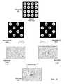
- FIG. 16shows a zoom into an example microlens array, and shows individual microlenses and (black) chromium mask between the microlenses.
- FIG. 7illustrates an example embodiment of focused plenoptic camera 200 with various other elements that may be integrated in the camera 200 .
- the objective lens 230 , the microlens array 220 , and the photosensor 210may be fixed.
- one or more of the above elementsmay be replaceable and/or adjustable.
- photosensor 210may be conventional film; in other embodiments, photosensor 210 may be a device for digitally capturing light, for example a CCD.
- a focused plenoptic camera 200 as described hereinmay include, in addition to main lens 230 , microlens array 220 , and photosensor 210 , any other type of elements and features commonly found in digital cameras or other cameras including light-field and plenoptic cameras and large-format film cameras, and may also include additional elements and features not generally found in conventional cameras.
- a full-resolution light-field rendering method for rendering high-resolution images from light-fields captured by focused plenoptic camera 200may be implemented in captured data processing module 260 .
- Captured data processing module 260may be implemented in hardware, software, or a combination thereof.
- light-fields captured by focused plenoptic camera 200may be rendered according to the full-resolution light-field rendering method implemented in a rendering module executing on a separate device, e.g. a computer system, to generate one or more high-resolution output images of a captured scene, as described herein.
- An example computer system in which embodiments of the full-resolution light-field rendering method may be implementedis illustrated in FIG. 24 .
- a focused plenoptic camera 200may include a shutter 314 . Shutter 314 may be located in front of or behind objective lens 230 .
- a focused plenoptic camera 200may include one or more processors 300 .
- a focused plenoptic camera 200may include a power supply or power source 304 , such as one or more replaceable or rechargeable batteries.
- a focused plenoptic camera 200may include a memory storage device or system 302 for storing captured light-field images and/or rendered final images or other information such as software.
- the memory 302may be a removable/swappable storage device such as a memory stick.
- a focused plenoptic camera 200may include a screen 306 (e.g., an LCD screen) for viewing scenes in front of the camera prior to capture and/or for viewing previously captured and/or rendered images. The screen 306 may also be used to display one or more menus or other information to the user.
- a focused plenoptic camera 200may include one or more I/O interfaces 312 , such as FireWire or Universal Serial Bus (USB) interfaces, for transferring information, e.g. captured light-field images, software updates, and so on, to and from external devices such as computer systems or even other cameras.
- a focused plenoptic camera 200may include a shutter release 308 that is activated to capture a light-field image of a subject or scene.
- a focused plenoptic camera 200may include one or more controls 310 , for example controls for controlling optical aspects of the focused plenoptic camera 200 such as shutter speed, one or more controls for viewing and otherwise managing and manipulating captured images stored in a memory on the camera, etc.
- An adjustable focused plenoptic camera 200may include one or more controls for adjusting the relative location of (the distance between) the components in the camera 200 , such as the distance b between microlens array 220 and photosensor 210 .
- An adjustable focused plenoptic camera 200may include one or more manual or automatic adjusting mechanism(s) 320 , or adjusters, configured to adjust the relative location of (the distance between) the components in the camera 200 , such as the distance b between microlens array 220 and photosensor 210 .
- the adjusting mechanisms 320may act to adjust one or more components responsively to controls 310 .
- FIG. 8illustrates an example embodiment of a focused plenoptic camera 200 based on a large-format film camera.
- large-format film camera embodimentsare capable of up to 1 gigapixel, or even higher, resolution for the flat (a flat is a 2D representation of the 4D radiance).
- An example embodimentmay, for example, be implemented in large-format film camera using a 135 mm objective lens 430 and 4 ⁇ 5 format film as the “photosensor” (in large-format cameras, single negatives of film are generally placed in a film holder 402 or cartridge that can be inserted into and removed from the camera body).
- Focused plenoptic camera 400includes a microlens array 406 .
- FIG. 16shows a zoom into an example microlens array, and shows individual microlenses and (black) chromium mask between the microlenses.
- the microlens array 406may include 146,000 microlenses of diameter 0.25 mm and focal length 0.7 mm.
- Other configurations of microlens array 406including different numbers of microlenses and/or microlenses with different optical characteristics, are possible and anticipated.
- a mechanism inside a film holder 402 of the large-format film cameraholds the microlens array 406 so that the flat side of the glass base of the array 406 is pressed against the film.
- the thickness of the microlens array 406is such that, when placed against the film, the microlenses are distance f from the film.
- Other configurations of microlens arrays 406are possible, and the configuration of the large-format film camera makes it possible to easily change configurations of microlenses by simply using a different microlens array 406 .
- Microsheets 404 of glassmay be used in the assembly as spacers or shims between the microlens array 406 and the film in film holder 402 to increase the distance from the microlenses and the film to be greater than f (e.g., 4/3 f).
- An example thickness of a microsheet 404 that may be usedis 0.23 mm.
- Inserting microsheet glass 404provides spacing in a rigorously controlled manner. In one embodiment, additional spacing may be created by adding a single microsheet 404 between the film holder 402 and the microlens array 406 in order to displace the microlenses by an additional 1 ⁇ 3 f, approximately 0.2 mm from the sensor. Additional microsheets 404 may be added to provide additional spacing. In some embodiments, other mechanisms than microsheet glass may be used as spacers between the microlens array 406 and film holder 402 to adjust the distance between the microlens array 406 and film holder 402 .
- the film holder 402 and microlens array 406may be coupled to create assembly 410 .
- One or more microsheets 404may optionally be inserted between the film holder 402 and microlens array 406 to provide additional spacing as necessary or desired.
- the assembly 410may then be inserted into the large-format film camera.
- the combination of the large-format film camera and the assembly 410effectively forms a focused plenoptic camera 400 .
- Focused plenoptic camera 400may then be used to capture a flat of a scene on the film in film holder 402 .
- a flatis a 2D representation of the 4D lightfield.
- the assembly 410may then be removed from the camera 400 , disassembled, and the film may be appropriately processed.
- the film negative and/or a print of the flatmay then be digitized, for example using a high-resolution scanner or a device that generates digital images from negatives.
- the digitized flatmay be stored to a storage device, such as a disk drive, DVD, CD, etc.
- the digitized flatmay be rendered according to the full-resolution light-field rendering method, implemented in a rendering module executing on a computer system, to generate one or more high-resolution output images of the scene as described herein.
- An example computer system in which embodiments of the full-resolution light-field rendering method may be implementedis illustrated in FIG. 24 .
- Embodiments of a method and apparatus for rendering high-resolution images from a light-fieldare described.
- the method for rendering high-resolution images from the light-fieldmay be referred to as a full-resolution light-field rendering method.
- the light-field rendering methodmay be referred to as full-resolution because the method makes full use of both positional and angular information available in the captured radiance data.
- the full-resolution light-field rendering methodmay be implemented as or in a tool, module, library function, plug-in, stand-alone application, etc.
- implementations of embodiments of the full-resolution light-field rendering methodmay be referred to as a rendering module.
- other light-field rendering or processing techniquesmay be applied to captured flats by a rendering module, and/or by other modules.
- FIG. 24illustrates an example computer system on which embodiments of a rendering module may be implemented.
- the full-resolution light-field rendering methodmay be derived by analyzing the optical system of the plenoptic camera. First, some observations of captured flats, which are 2D representations of the 4D light-field, are presented, and these observations are used to motivate the subsequent analysis.
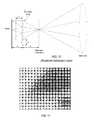
- FIG. 9shows an example crop from a raw flat captured with a plenoptic camera.
- repeated edges inside multiple circlesmay be observed.
- Each microlens in the microlens arraycreates a microimage; the resulting flat is thus an array of microimages.
- the overall imagemay be perceived, whereas the correspondence between the individual microlens images and the large scale scene is less obvious.
- edgesare often repeated from one circle to the next.
- the same edge (or feature)may be seen in multiple circles, in a slightly different position that shifts from circle to circle. If the main camera lens is manually refocused, a given edge can be made to move and, in fact, change its multiplicity across a different number of consecutive circles.
- Repetition of features across microlensesis an indication that that part of the scene is out of focus.
- the same featureappears only once in the array of microimages.
- Keplerian telescopicwhere the distance between the photosensor and the microlens array, b, is greater than the focal length f of the microlenses in the array
- Galilean telescopicalso referred to as binocular
- bis less than f
- FIG. 10illustrates the Keplerian telescopic case (b>f) for a plenoptic camera.
- a plenoptic cameramay be considered as an array of (Keplerian) telescopes with a common objective lens. (For the moment the issue of microlenses not being exactly focused for that purpose will be ignored.)
- Each individual telescope in the arrayhas a microcamera (an eyepiece lens and the eye) inside the big camera. Just like any other camera, this microcamera is focused onto one single plane, and maps the image from the plane onto the retina, inverted and reduced in size.
- a cameracan be focused only for planes at distances ranging from f to infinity ( ⁇ ) according to the lens equation:
- a, b, and fhave the same meaning as for the big camera, except on a smaller scale. It can be seen that since a and b must be positive, it is not possible to focus closer than f. In a conventional plenoptic camera, the image plane is fixed at the microlenses. It may be more natural to consider the image plane fixed at distance f in front of the microlenses. In both cases, microimages are out of focus.
- FIG. 11shows a crop from the roof area in FIG. 9 .
- FIG. 11may be used to visually illustrate the Keplerian “telescopic” behavior. It is possible to observe in FIG. 11 that the edge is repeated two times when moving away from the roof. The farther from the roof a circle is, the farther the edge appears inside that circle. Moving in any given direction, the edge moves relative to the circle centers in the same direction. Once detected in a given area, this behavior is consistent (valid in all directions in that area). Careful observation shows that images in the small circles are indeed inverted patches from the high-resolution image, as if observed through a telescope.
- a practical range for bmay be f ⁇ b ⁇ 1.5 f.
- FIG. 12illustrates the Galilean telescopic, or binocular, case (b ⁇ f) for a plenoptic camera.
- FIG. 13shows a crop from the tree area in FIG. 9 , and is used to illustrate details of Galilean telescopic imaging in light-field cameras. Note that the image is not inverted in FIG. 13 .
- a plenoptic cameramay also be considered as an “incompletely focused” camera, i.e., a camera focused behind the film plane (as in a Galilean telescope and in binoculars). If an appropriate positive lens is placed in front of the film, the image would be focused on the film. For a Galilean telescope, this is the lens of the eye that focuses the image onto the retina.
- the microlensesFor a plenoptic camera, this role is played by the microlenses with focal length f.
- the microlensesIn the Galilean telescopic case, the microlenses would need to be placed at a distance smaller than f from the film. Note also that while the Keplerian telescopic operation inverts the inside image, the Galilean telescopic operation does not invert it.
- Keplerian telescopic imagingcharacteristic behavior of Galilean telescopic imaging can be observed in the plenoptic camera. See FIG. 13 , which is a crop from the top left corner in FIG. 9 .
- FIG. 13it can be observed that edges are repeated about two or three times when moving away from the branch. The farther from the branch, the closer to the branch the edge appears inside the circle. Moving in any given direction, the edge moves relative to the circle centers in the opposite direction. Once detected in a given area, this behavior is consistent (valid in all directions in that area). This is due to the depth in the image at that location. Careful observation shows that images in the small circles are in fact patches from the corresponding area in the high-resolution image, only reduced in size. The more times the feature is repeated in the circles, the smaller it appears and thus a bigger area is imaged inside each individual circle.
- an approximately focused plenoptic camerai.e., a plenoptic camera where b ⁇ f
- a plenoptic camerawhere b ⁇ f
- Each microcameraimages only a small part of that plane. The shift between those small images is obvious from the geometry, as explained below in the section titled Analysis. If at least one microcamera could image this entire plane, it could directly capture a high-resolution image. However, the small images are limited in size by the main lens aperture.
- the magnification of these microcamera images, and the shift between them,is defined by the distance to the image plane.
- This distancecan be at positive or negative distance from the microlenses, corresponding to the Keplerian telescopic (positive) and Galilean telescopic (negative) cases described above.
- embodimentscan make use of the Keplerian telescopic or Galilean telescopic behavior to generate a high-resolution image from the flat. This process is described in the following sections.
- microlensesmay not be focused exactly on the plane that is to be imaged, causing the individual microlens images to be blurry. This may limit the amount of resolution that can be achieved. One way to improve such results would be deconvolution. Another way would be to stop down the microlens apertures.
- FIGS. 14A and 14Bthe case of a “plenoptic” camera using a pinhole array instead of microlens array is considered.
- pinhole imagesproduce no defocus blur, and in this way are perfect. But this is in theory; in the real world, pinholes are replaced with finite but small apertures and microlenses.
- the full-resolution light-field rendering methodmay execute a different action based on which behavior is observed in the microimages contained in the flat captured by a focused plenoptic camera.
- the full-resolution light-field rendering methoddetects edges (or features) moving relative to the microimage centers (the microimages are generally circular, so may be referred to as circles) in the same direction as the direction of movement, all microimages in that area are inverted relative to their individual centers (this is the Keplerian telescopic case).
- examination of the microimages to determine the direction of movement of edgesmay be performed by a user via a user interface.
- the usermay mark or otherwise indicate areas that the user determines need be inverted via the user interface.
- examination of the microimages to determine the direction of movement of edgesmay be performed automatically in software.
- the small circles, or microimages, in a flatare, effectively, puzzle pieces of the big image, and embodiments of the full-resolution light-field rendering method reproduce the big image by bringing the microimages sufficiently close together.
- the big imagemay also be reproduced by enlarging the pieces so that features from any given piece match those of adjacent pieces. Assembling the resized pieces reproduces exactly the high-resolution image.
- FIG. 15illustrates a lens circle (or microimage) of diameter D and a patch of size m 1 ⁇ m 2 , where at least one of m 1 and m 2 is an integer greater than or equal to 2.
- Embodiments of the full-resolution light-field rendering methodusing the algorithm described above, produce a gain in resolution that is approximately equal to the number of pixels m 1 ⁇ m 2 in the original patches. That is, embodiments produce m 1 ⁇ m 2 pixels, instead of one pixel, per microimage
- the distance (measured in number of focal lengths) to the image plane in front of the microlensis related to D and m.
- the optics of the microlens as a camerais the main factor in determining the quality of each microimage.
- Blurry images from optical devicesmay be deconvolved and the sharp image recovered to some extent.
- the effective kernel of the optical systemshould be known. While there are limitations in this related to bit depth and noise, embodiments may increase resolution up to m 1 ⁇ m 2 times the resolution of a conventional plenoptic camera and conventional rendering method. Example embodiments have demonstrated a 27 ⁇ increase of resolution in one plane, and a 10 ⁇ increase of resolution in another plane, when compared to conventional methods and apparatus, and without any deconvolution. Other embodiments may yield other increases in resolution when compared to conventional methods and apparatus.
- a focused plenoptic camera as described hereinmay be implemented in film cameras.
- Embodimentsmay, for example, be implemented in large-format film cameras.
- An example large-format film camera embodimentis illustrated in FIG. 8 .
- One example embodimentmay, for example, be implemented in large-format film camera using a 135 mm objective lens and 4 ⁇ 5 format film.
- a focused plenoptic camera based on a large-format film camera rather than on a digital cameramay be used for experimental purposes in order to avoid resolution constraint of digital sensors.
- film camera embodiments of the focused plenoptic camera designare practical and may have practical applications.
- large-format film camera embodimentsare capable of 1 gigapixel, or even higher, resolution for the flat (2D) representation of the 4D radiance (the raw flat).
- a component of the focused plenoptic camerais a microlens array.
- FIG. 16shows a zoom into an example microlens array, and shows individual microlenses and (black) chromium mask between the microlenses.
- the microlens arrayincludes 146,000 microlenses of diameter 0.25 mm and focal length 0.7 mm.
- a mechanism inside a 4 ⁇ 5 inch film holder of the large-format film cameraholds the microlens array so that the flat side of the glass base is pressed against the film.
- the thickness of the microlens arrayis such that, when placed against the film, the microlenses are distance f from the film.
- Other configurations of microlens arraysare possible, and the configuration of the large-format film camera makes it possible to easily change configurations of microlenses by simply using a different microlens array.
- Microsheets of glassmay be used in the assembly as spacers or shims between the microlens array and the film to increase the distance from the microlenses and the film to be greater than f (e.g., 4/3 f).
- An example thickness of a microsheet that may be usedis 0.23 mm. Inserting microsheet glass provides spacing in a rigorously controlled manner.
- additional spacingmay be created by adding a single microsheet between the film and the microlenses in order to displace the microlenses by an additional 1 ⁇ 3 f, approximately 0.2 mm from the sensor. Additional microsheets may be added to provide additional spacing.
- FIGS. 17 through 20are used to illustrate experimental results from applying the full-resolution rendering method to flats captured with the example focused plenoptic camera based on a large-format film camera described above.
- the operation of rendering in both the Keplerian telescopic case and the Galilean telescopic caseis illustrated and described.
- the original, unrendered flatwas generated by capturing the image on film using the example focused plenoptic camera based on a large-format film camera, and digitizing the image via a scanning process using a high-resolution scanner. A portion of the digitized flat is shown in FIG. 17 . After digitization, the full original flat is 24,862 ⁇ 21,818 pixels, of which 2,250 ⁇ 1,950 pixels are shown in FIG. 17 . The approximate region of the original flat extracted to produce FIG. 17 is shown by small solid white rectangle in FIG. 18C .
- FIGS. 18A through 18COutput images rendered from the flat using conventional rendering methods are shown in FIGS. 18A through 18C .
- the entire flatwas rendered with the conventional method, resulting in a 408 ⁇ 357 pixel image.
- FIG. 18Ais rendered at 300 ppi
- FIG. 18Cis rendered at 72 ppi. At 300 ppi, the image is only about 1 inch by 1 inch.
- FIG. 18Bshows a 27 ⁇ magnification of a crop of the curb area from the 300 ppi image in FIG. 18A .
- the solid white rectangle in FIG. 18Cshows the region from the light-field shown in FIG. 17 .
- the dashed white rectangle in FIG. 18Cshows a region that is rendered according to an embodiment of the full-resolution light-field method as shown in FIGS. 19 and 20 .
- FIG. 19show a full-resolution rendering of the experimental light-field, rendered assuming the Keplerian telescopic case according to one embodiment of the full-resolution light-field rendering method described herein.
- This region of the imageis shown by the dashed white rectangle in FIG. 18C .
- the scaling-down factorwas taken to be approximately 2.4, so that the full-resolution rendered image measured 11016 ⁇ 9666, i.e., over 100 megapixels. Even though the image is at 300 dpi, only a 2,250 ⁇ 1,950 region is shown in FIG. 19 .
- the imageis well-focused at full-resolution in the region of the house, but not well-focused on the tree branches.
- FIG. 20shows a full-resolution rendering of the experimental light-field, rendered assuming the Galilean telescopic case according to one embodiment of the full-resolution light-field rendering method described herein. This region of the image is shown by the dashed white rectangle in FIG. 18C . Note that, in contrast to the image in FIG. 20 , this image is well-focused at full-resolution in the region of the tree branches but not well-focused on the house.
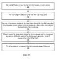
- FIG. 21is a flow chart illustrating how light is directed within a focused plenoptic camera according to one embodiment.
- light from a sceneis received at the main lens of a focused plenoptic camera.
- FIGS. 6 , 7 and 8illustrate example focused plenoptic cameras.
- the received lightis refracted by the main lens to an image plane.
- an array of microlenses, the microlenses of which are focused on the image planerefracts light from the image plane onto a photosensor located, relative to the microlenses, at a distance that is a multiple of the focal length f of the microlenses.
- the distance between the microlenses and the photosensormay be 3 ⁇ 4 f, 4/3 f, 5/3 f, 1.5 f, and so on.
- different views of the image plane, refracted by the microlenses onto the photosensorare captured at different regions of the photosensor to generate a flat, which is a 2D representation of the 4D light-field.
- the photosensormay be a device configured to digitally capture light such as a CCD, while in other embodiments the photosensor may be conventional film.
- the captured flatmay be rendered to produce a final high-resolution image, or images, of the scene, for example using a full-resolution light-field rendering method as described in FIG. 22 .
- the flatmay be digitized to generate a digitized flat before rendering.
- FIG. 22is a flowchart of a full-resolution light-field rendering method according to one embodiment.
- a flat captured by a focused plenoptic cameramay be obtained (see, e.g., FIG. 9 for an example of what such a flat may look like to a human observer).
- microimages in areas of the flatmay be examined (manually or automatically, as described below) to determine the direction of movement of edges in the microimages relative to a direction of movement of the algorithm.
- the microimages in that areamay be inverted relative to their individual centers. If the edges are not moving relative to the microimage centers in the same direction as the direction of movement (i.e., if the edges are moving in the opposite direction as the direction of movement), then the microimages in the area are not inverted.
- examination of the microimages to determine the direction of movement of edgesmay be performed manually by a user via a user interface. The user may mark or otherwise indicate areas that the user determines need be inverted via the user interface.
- examination of the microimages to determine the direction of movement of edgesmay be performed automatically in software.
- an automated software methodmay examine the microimages to determine noise in the microimages, for example using a Fourier transform to detect peaks at certain frequencies. An excessive amount of noise in an area of the final rendered image may indicate that microimages in that area are flipped, and thus need to be inverted. Microimages that include noise over a specified threshold may be marked to be inverted.
- the microimagesmay each be cropped to produce an m 1 ⁇ m 2 subregion or crop of each microimage, where at least one of m 1 and m 2 is an integer greater than two.
- the subregions or crops from the microimagesmay be appropriately assembled to produce a final high-resolution image of the scene.
- the microimagesthemselves may be appropriately assembled to produce a final high-resolution image of the scene.
- element 806is not performed; at 808 , the microimages are assembled to produce an output image.
- overlapping portions of adjacent microimagesmay be merged, blended, or otherwise handled.
- two or more images rendered from a flat according to rendering methods described hereinmay be combined to produce a higher-quality output image.
- the microimages in a flatmay all be inverted, and the inverted microimages appropriately assembled to produce a first intermediate image.
- a second intermediate imagemay be generated without inverting the microimages prior to assembling.
- the two intermediate imagesmay then be combined to produce a higher-quality output image.
- the combination of the two imagesmay be performed manually by a user via a user interface, for example using a selection tool to select portions of an image to be combined with the other image, or alternatively may be performed automatically in software, for example using a noise detection technique as described above to find excessively noisy regions of one or both intermediate images.
- the usermay manually (or software may automatically) select areas in one intermediate image that are of higher quality than the same areas in the other image, and then combine the selected areas with the other image to produce an output image that includes the highest quality portions of the two intermediate images.
- a mape.g., a bitmap
- the output imagemay be generated from the two intermediate images according to the map.
- more than two intermediate imagesmay be generated, and a similar method may be used to generate a higher-quality output image from the intermediate images.
- FIG. 25is a flowchart of a full-resolution light-field rendering method in which multiple images are rendered from a flat and combined to produce a final high-resolution output image, according to some embodiments.
- a flat captured by a focused plenoptic cameramay be obtained (see, e.g., FIG. 9 for an example of what such a flat may look like to a human observer).
- the plurality of microimagesmay be assembled to produce a first high-resolution image.
- each of the microimagesmay be inverted relative to their respective centers to produce a plurality of inverted microimages.
- the plurality of inverted microimagesmay be assembled to produce a second high-resolution image.
- the first high-resolution imagemay be combined with the second high-resolution image to produce a final high-resolution image.
- the combination of the two imagesmay be performed manually by a user via a user interface, for example using a selection tool to select portions of an image to be combined with the other image, or alternatively may be performed automatically in software, for example using a noise detection technique as described above to find excessively noisy regions of one or both intermediate images.
- FIG. 26shows an example full-resolution rendering of a light-field in which foreground and background portions of the example images shown in FIGS. 19 and 20 have been combined to produce a higher-quality output image.
- the foreground portion (the tree) of FIG. 19has been replaced with the corresponding foreground portion of FIG. 19 .
- the selectionmay be performed manually, for example by a user via a user interface, or alternatively may be performed automatically in software, for example using a noise detection technique as described above to select images with lower levels of noise in one or more frequencies.
- two or more of the imagesmay be selected and combined to generate a higher-quality output image.
- the combination of the imagesmay be performed manually or automatically.
- inversion and cropping of microimagesmay be combined in a single automatic operation.
- a negative value for (m 1 , m 2 )may be used to indicate that the microimages in the input flat or area are to be inverted, with a positive value for (m 1 , m 2 ) indicating that the microimages are not to be inverted.
- Other methods to indicate whether microimages are to be invertedmay be used.
- inversion and cropping of microimagesmay be performed in various combinations on an input flat to render multiple rendered images according to the combinations.
- some imagesmay be rendered using a range of values for m 1 and m 2 as described above while also inverting the microimages, while other images may be rendered using a range of values for m 1 and m 2 as described above in which the microimages are not inverted.
- One or more of the rendered imagesmay then be manually or automatically selected as output image(s).
- two or more of the rendered imagesmay be combined as previously described (see, e.g., FIG. 26 ) to produce an output image.
- microlenses with different focal lengthsare described.
- all of the microimagesare captured at the same time in a single image (referred to as a flat) at the sensor.
- the microlenses with different focal lengthsfocus on different planes within the image created by the main lens of the camera, and project microimages from these different planes onto the photosensor.
- multiple microimages of the same scenemay be captured at different focal lengths in a single flat at the same time with a focused plenoptic camera.
- Different ones of the microimages captured at different focal lengthsare in focus at different planes of the image created by the main lens of the camera.
- Flats captured using embodiments of a focused plenoptic camera with microlenses of different focal lengthsmay be used to generate multiple images each captured at a different focal length.
- the different views of the scene captured by the different microlensesare identical or nearly identical 3D views of the scene, that is identical or nearly identical images all captured at the same time, but captured at different focal lengths.
- Imaging functions, such as focus bracketing and refocusingmay be performed on the flat to produce precise and high quality output images.
- the main camera lenscreates an image “in the air” at the focal plane. This may be referred to as the main image.
- This imageis observed by an array of microlenses that are focused on the main image (and not on the main lens). Based on the multiple microlenses (which may be viewed as multiple microcameras), each point in the main image is re-imaged two or more times on to the sensor, and thus each point in the main image is captured in two or more of the microimages at the sensor. This is true for both the Keplerian telescopic mode and the Galilean telescopic (or binocular) mode of a focused plenoptic camera.
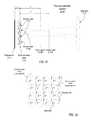
- FIGS. 27A and 27Billustrate the different modes or configurations of a focused plenoptic camera according to some embodiments.
- FIG. 27Aillustrates the Keplerian telescopic mode
- FIG. 27Billustrates the Galilean telescopic, or binocular, mode.
- the main imagein the Keplerian telescopic mode, the main image is real and is in front of the sensor.
- FIG. 27Bin Galilean telescopic mode, the main image is virtual, and is behind the sensor. In both modes, the main image is re-imaged to the sensor multiple times.
- the unobstructed diameters of the microlensesare the same, denoted as d.
- the distances a and b and the focal length of the microlensessatisfy the lens equation. Note that, in Galilean mode, a is negative.
- Conventional plenoptic camerasprovide the capability to focus and refocus images from a single flat after the flat is captured.
- conventional plenoptic camerasrequire extremely high pixel size of the captured image in order to create quality refocused images.
- embodiments of the focused plenoptic camera as previously describedare more efficient than conventional plenoptic cameras.
- artifactsmay still be observed with large changes in focus if the input data is insufficient.
- Embodiments of focused plenoptic cameras employing microlenses with different focal lengthsare described that may leverage the characteristics of the focused plenoptic camera as described herein to produce quality output images that are in-focus at different depths.
- the focused plenoptic camerasimultaneously captures multiple, almost identical, microimages
- embodiments of a focused plenoptic camera that include microlenses with at least two different focal lengthsmay be used to simultaneously capture microimages from at least two different focal planes created by the main camera lens at different distances from the microlens array.
- a focused plenoptic camera that includes microlenses with two different focal lengthsmay capture some of the microimages from one focal plane at a distance a from the microlens array, and capture others of the microimages from another focal plane at a different distance a′ from the microlens array.
- a focused plenoptic camera that includes microlenses with n different focal lengthsmay be considered as essentially the equivalent of n focused plenoptic cameras in one.
- Each of these n “cameras”has an amount of 3D capability, but each “camera” is focused at a different depth. Image operations such as refocusing and focus bracketing are thus made possible from such “multiple camera” data. Since all of the microimages in a flat are captured by the focused plenoptic camera at the same time, there is no problem with changing scenes in the field of view as there is when using conventional cameras to perform focus bracketing by capturing a sequence of temporally different images.
- imagesmay be constructed from subsets of the microimages captured using each type of microlens, thus creating n images each focused at a different depth.
- An advantage of this approach when compared to a focused plenoptic camera with microlenses all of the same focal length and with infinite depth of field in each microlensis that larger apertures may be used, and thus a lower F-number may be used. This results in a faster camera (capturing more of the light), which generally results in better quality images.
- focusingis performed optically and not digitally, thus requiring less data to be saved and less data processing to be performed.
- different optical elements that provide two or more different focal lengthsmay be used in a focused plenoptic camera such as camera 200 illustrated in FIGS. 6 and 7 and camera 400 illustrated in FIG. 8 .
- a focused plenoptic camerasuch as camera 200 illustrated in FIGS. 6 and 7 and camera 400 illustrated in FIG. 8 .
- an alternating pattern (or some other pattern) of microlenses of two or more different focal lengthsmay be provided in a microlens array.
- a raw image or “flat” captured using the microlens arrayincludes multiple microimages captured at the different focal lengths according to the two or more different microlenses of different focal lengths.
- One or more different imagesmay then be assembled from the microimages, with each image assembled from microimages captured using the microlenses of one of the different focal lengths.
- Each of these images“captures” the scene in front of the camera at a different focal plane.
- a final imagemay then be generated by appropriately combining two or more of the images assembled from the microimages, for example by combining in-focus regions of one image with in-focus regions of another object.
- imagesmay be assembled from the microimages by first combining the microimages and then assembling the combined microimages to produce one or more output images.
- Example methods for assembling microimages from a flat captured by a focused plenoptic camera to generate an image or imagesare shown in FIGS. 22 and 25 .
- a single image or “flat”may be captured using the camera.
- the flatconsists of multiple microimages, each corresponding to a microlens in the microlens array. From this single flat, two or more different images may be generated by appropriately assembling the microimages. The two or more images exhibit different focusing characteristics according to the respective microlenses that captured the microimages from which the images are assembled. This allows, for example, a single flat to be captured of an action scene, such as a sporting event or wildlife; from that flat, multiple images captured at different focal lengths and thus exhibiting different focusing characteristics may be generated.
- Thisallows a photographer to take a single “snapshot” of an action scene, and from that single image (the flat), produce two or more images of the same scene. Since the images were all captured at the same time in a single flat, the images are essentially identical except that each is focused differently. The photographer may then select a best-focused image from among the different images. Alternatively, using appropriate image processing tools, the photographer may choose to assemble a composite image from the multiple images that incorporates different regions from different images that are in-focus.
- the microimages from a raw flat captured with a focused plenoptic camera employing microlenses with different focal lengthsmay first be combined to generate a combined flat (a flat including the combined microimages).
- the microimages from the combined flatmay then be appropriately assembled to produce one or more output images.
- Combining the microimages to generate a combined flatmay allow the combined flat to be used in generating 3D views, parallax generation, and in general in any of various light-field operations that may be performed on a flat captured with a focused plenoptic camera.
- Embodimentsare described in which an array of single microlenses including at least two different microlenses with different focal lengths are employed; in these embodiments, each single lens may be considered an optical element.
- Embodimentsare also described in which an array of stacks of two (or potentially more) microlenses including at least two different stacks that provide different focal lengths are employed; in these embodiments, each stack of two (or more) microlenses may in combination be considered as a single optical element.
- the lens stacksmay be provided by stacking two microlenses arrays, for example microlens arrays manufactured on silica wafers as described later in this document, on top of each other in the camera.
- one of the two microlens arraysincludes microlenses all of the same focal length, while the other microlens array includes at least two different microlenses of different focal lengths.
- the different microlensesmay also provide different depths of field.
- FIG. 28is a block diagram illustrating a focused plenoptic camera, for example as illustrated in FIG. 6 , including different microlenses with different focal lengths and depths of focus, according to some embodiments. Note that, in FIG. 28 , as in the other Figures, the distances between elements, the sizes of the elements, and the relative sizes of the elements when compared to each other are illustrative and are not intended to be limiting.
- Focused plenoptic camera 2000may include a main (objective) lens 2030 , a microlens array 2020 , and a photosensor 2010 .
- photosensor 2010may be conventional film; in other embodiments, photosensor 2010 may be a device for digitally capturing light, for example a CCD.
- the microlens array 2020includes microlenses 2022 of two different focal lengths, designated by f and f′.
- Microlenses 2022 fhave a shorter focal length f than microlenses 2022 f ′ with focal length f′.
- Microlenses 2022 fare focused on focal plane 2040 a of the main lens 2030 ; focal plane 2040 a is at distance a from the microlens array 2020 .
- Microlenses 2022 f ′are focused on focal plane 2040 a ′ of the main lens 2030 ; focal plane 2040 a ′ is at distance a′ from the microlens array 2020 .
- FIG. 29illustrates a portion of a microlens array including and alternating pattern of microlenses of two different focal lengths f and f′, according to some embodiments.
- the microlens arraymay be manufactured as a wafer, for example a glass or fused silica wafer, with the microlenses integrated into or deposited onto the wafer.
- FIG. 16shows a zoom into an actual image of an example microlens array, and shows individual microlenses and (black) chromium mask between the microlenses. Referring to FIG. 29 , the white circles represent microlenses in the array.
- Each microlensmay have a diameter of, for example, 240 microns.
- the distance between the centers (the optical axes) of the microlensesmay be, for example, 250 microns. Other diameters and/or pitches may be used in various embodiments. While FIG. 29 shows the microlenses arranged in a regular grid pattern, other patterns or arrangements of microlenses may be used in various embodiments. Also, while FIG. 29 shows the microlenses as all the same diameter, microlenses of different focal lengths may have different diameters.
- microlenses with different focal lengths in the microlens arrayone or more of microlens diameter, microlens thickness, and microlens material may be varied.
- Various manufacturing techniquesmay be employed to create microlenses with different focal lengths in an array, for example on a silica wafer.
- the black region of FIG. 29represents a mask or masking on the microlens array to prevent light passing through the microlens array except through the microlenses.
- the appropriate masked regionmay be coated with an opaque material or substance, such as black chromium.
- the maskmay be deposited on one wafer, while the microlenses are manufactured on another wafer; the two wafers may then be combined to create the microlens array.
- Other methods of manufacturing a microlens array and/or of applying a mask to a microlens arraymay be used.
- the maskis deposited so that all of the microlenses, including the microlenses of different focal lengths, have the same aperture to within the precision of the manufacturing process.
- FIGS. 28 and 29show microlenses of two different focal lengths in a microlens array
- embodimentsmay include microlenses of n different focal lengths producing n different planes of focus, or focal planes.
- FIG. 30shows an example microlens array including an alternating pattern of microlenses of four different focal lengths (f, f′, f′′, and f′′′), according to some embodiments, which would produce four different focal planes.
- the parameters a, b, and fmay vary.
- the parameter bis fixed.
- a minification metric Mmay be defined as:
- Ma b
- Mspecifies how many times the main image in front of the microlenses is reduced when mapped to the sensor. Since the microlenses in the microlens array are at the same pitch (the distance between the optical axes), and each point in the main image should be imaged at least once by each type of microlens, for the microlens arrangement of FIGS. 28 and 29 with two different focal lengths, M should be greater than 2 (M>2).
- M>nfor a one-dimensional camera (i.e., a row of different microlenses in a microlens array), where n is the number of different cameras in the row. Note that the same applies to a column.
- the parameters f and b of the microlens arraydefine both M and the plane of best focus, a.
- imagesmay be constructed from subsets of the microimages captured using each type of microlens, thus creating n images each focused at a different depth.
- One or more image processing techniquesmay be applied to two or more of these n images to produce a combined image that incorporates in-focus regions of the two or more images.
- FIG. 28illustrates embodiments of a focused plenoptic camera with a microlens array including different microlenses with different focal lengths. These embodiments employ an array that provides a pattern of single microlenses with different focal lengths.
- Embodiments of a focused plenoptic camera that employ stacks of two or more microlenses in a microlens array, or alternatively two or more microlens arrays that when combined provide the microlens stacks,are described.
- stacks of two or more microlensesmay be used in an array of optical elements (considering the two or more microlenses in a stack as one optical element) that provide different focal lengths and depths of field.
- FIG. 31is a block diagram illustrating a focused plenoptic camera, for example as illustrated in FIG. 6 , including stacks of two or more microlenses in a microlens array with different focal lengths provided by different microlens stacks, according to some embodiments. Note that, in FIG. 31 , the distances between elements the sizes of the elements, and the relative sizes of the elements when compared to each other are illustrative and are not intended to be limiting.
- Focused plenoptic camera 2100may include a main (objective) lens 2130 , an array 2120 of microlens stacks, and a photosensor 2110 .
- photosensor 2110may be conventional film; in other embodiments, photosensor 2110 may be a device for digitally capturing light, for example a CCD.
- array 2120includes microlens stacks 2122 that provide two different focal lengths, which may be designated by ⁇ and ⁇ ′.
- Microlens stack 2122 Aprovides a shorter focal length ⁇ than microlens stack 2122 B, which provides focal length ⁇ ′.
- Microlens stacks 2122 Aare focused on focal plane 2140 a of the main lens 2130 ; focal plane 2140 a is at distance a from the microlens array 2120 .
- Microlens stacks 2122 Bare focused on focal plane 2140 a ′ of the main lens 2130 ; focal plane 2140 a ′ is at distance a′ from the microlens array 2120 .
- the microlenses on the sensor side of the microlens stacksmay all be identical, while the microlenses on the main lens side of the microlens stacks may differ to provide the different focal lengths.
- Other arrangements of microlenses in the stacksare possible.
- FIG. 32illustrates a portion of an example array including an alternating pattern of microlens stacks that provide different focal lengths ⁇ and ⁇ ′, according to some embodiments.
- the white circlesrepresent microlenses in the microlens stacks.
- the array of microlens stacksmay be viewed as two separate arrays of microlenses, with one of the two arrays closer to the photosensor, and the other array closer to the main lens.
- the microlenses in the array closer to the sensorall have a focal length of f.
- the microlenses in the array closer to the main lenshave alternating focal lengths of f′ and f′′. Note that embodiments in which both arrays include microlenses with different focal lengths are possible.
- Stack 2222 Aincludes a microlens with a focal lengths of f′; the microlenses in stack 2222 A act together to produce a focal length of ⁇ .
- Stack 2222 Bincludes a microlens with a focal lengths of f′′; the microlenses in stack 2222 B act together to produce a focal length of ⁇ ′. While FIG. 32 shows the microlens stacks arranged in a regular grid pattern, other patterns or arrangements of microlens stacks may be used in various embodiments.
- an array of microlens stacksmay be formed by combining two separate microlens arrays. For example, one microlens array that includes microlenses all of the same focal length may be combined with another microlens array that includes microlenses of n different focal lengths, with the microlenses in the arrays aligned on their optical axes, to form an array of microlens stacks.
- FIG. 33illustrates portions of two example microlens arrays that may be combined to form an array of microlens stacks, according to some embodiments.
- Microlens array 2300includes an alternating pattern of microlenses of two different focal lengths f′ and f′′.
- Microlens array 2310includes a pattern of microlenses of focal length f.
- the microlens arraysmay be manufactured as wafers, for example as glass or fused silica wafers, with the microlenses integrated into or deposited onto the wafer.
- FIG. 16shows a zoom into an actual image of an example microlens array, and shows individual microlenses and (black) chromium mask between the microlenses. Referring to FIG. 33 , the white circles represent microlenses in the array.
- Each microlensmay have a diameter of, for example, 240 microns.
- the distance between the centers (the optical axes) of the microlenses(referred to as the pitch) may be, for example, 250 microns.
- both microlens arrayshave the same pitch. Other diameters and/or pitches may be used in various embodiments. While FIG. 33 shows the microlenses arranged in the microlens arrays in a regular grid pattern, other patterns or arrangements of microlenses may be used in various embodiments. Note that the centers of the microlenses in array 2300 are aligned with the centers of the microlenses in array 2310 .
- microlensesmay be varied.
- microlensesmay be created by depositing an array of very small droplets of an appropriate material on a silica wafer, and then evenly heating the wafer to cause the droplets to spread. If the same amount of material is used in each droplet, then all of the resulting microlenses will be of the same diameter and thus of the same focal length, to within the precision of the manufacturing process. By depositing different amounts of material in different droplets, the resulting microlenses will be of different diameters and thus of different focal lengths.
- the black region of the microlens arrays shown in FIG. 33represents masking on the microlens arrays to prevent light passing through the microlens arrays except through the microlenses.
- the appropriate masked regionmay be coated with an opaque material or substance, such as black chromium.
- the maskmay be deposited on one wafer, while the microlenses are manufactured on another wafer; the two wafers may then be combined to create the microlens array.
- Other methods of manufacturing a microlens array and/or of applying a mask to a microlens arraymay be used.
- the maskis deposited so that all of the microlenses, including the microlenses of different focal lengths, have the same aperture to within the precision of the manufacturing process.
- FIG. 33show microlenses of two different focal lengths in microlens array 2300
- embodimentsmay include microlenses of n different focal lengths producing n different planes of focus, or focal planes.
- FIG. 30shows an example microlens array including an alternating pattern of microlenses of four different focal lengths (f, f′, f′′, and f′′′), according to some embodiments, which would produce four different focal planes; a similar microlens array could be used in combination with a microlens array such as array 2310 to produce an array of microlens stacks.
- the microlensesare formed on one side of the wafer.
- one side of a microlens arraywill generally be flat, with the other side including the microlenses.
- the microlens arraysmay be placed with the microlenses facing each other, with one array's microlenses facing the other array's flat side, or with both flat sides facing each other. While all these arrangements are possible, an arrangement with the microlenses facing each other, as shown in FIG.
- microlenses in the microlens array with microlenses of different focal lengthsare facing the flat side of the microlens array including microlenses all of the same focal length, as shown in FIG. 34B , are discussed below.
- FIG. 34Ashows two example microlens arrays with the microlenses facing each other, according to some embodiments.
- FIG. 34Ashows a cross-section of a row of four microlenses in each of two microlens arrays 2300 and 2310 that have been combined with the microlenses facing each other. In this arrangement, there may essentially be zero distance between the arrays of lenses. The distance between two stacked microlenses in this arrangement may thus be assumed to be zero.
- Array 2300may have two or more types of longer focal length microlenses that are used as corrections to the focal length of the microlenses in array 2310 . In this example, microlenses of two focal lengths, f′ and f′′, are shown. The following analysis is performed using the microlens with focal length f′.
- the combined focal length of two lenses, f and f′, placed on top of each other as shown in FIG. 34Amay be given by:
- FIG. 35graphically illustrates the above.
- lenses, f and f′are assumed to be placed at the same location. Note that the focal length f′ of the long-focus lens is exactly equal to the distance from the lens plane to the plane of best focus, and that minification (M) is
- FIGS. 34A and 35illustrate the case where the microlenses are placed next to each other, and thus the distance between the stacked microlenses may be assumed to be zero.
- FIG. 34Billustrates an arrangement in which the microlenses in the microlens array with microlenses of different focal lengths are facing the flat side of the microlens array including microlenses all of the same focal length, according to some embodiments.
- FIG. 34Bshows a cross-section of a row of four microlenses in each of two microlens arrays 2300 and 2310 that have been combined with the microlenses of array 2300 facing the flat side of array 2310 . Thus there is some finite, non-zero distance between the stacked microlenses.
- Array 2300may have two or more types of longer focal length microlenses that are used as corrections to the focal length of the microlenses in array 2310 .
- microlenses of two focal lengths, f′ and f′′,are shown.
- the arrangement shown in FIG. 34Bis a more complex case than that shown in FIG. 34A .
- the microlenses in array 2310which have a short focal length, may need to be positioned close to the photosensor. Because the wafer may be relatively thick (for example 1 mm), and the focal length of the microlenses in the main microlens array (array 2310 ) is relatively short, the main microlens array (array 2310 ) may be positioned so that the microlenses are facing the photosensor.
- the longer focal length microlenses of the second arrayare positioned next to the flat side of array 2310 , and thus are at a finite but non-zero distance D from the shorter focal length microlenses of array 2310 due to the wafer thickness. This distance D needs to be accounted for in the calculations.
- focal length f′is a longer focal length than f.
- the total optical transfer matrix of a system consisting of two lenses and distance D between the lensesis:
- the processmay be represented in terms of principal planes, i.e. an imaginary system that is equivalent to the above but consists of two travels, x and y as shown in FIG. 36 , and one lens:
- T ⁇ ( y ) ⁇ L ⁇ ( ⁇ ) ⁇ T ⁇ ( x )[ 1 - y ⁇ x + y - x ⁇ ⁇ y ⁇ - 1 ⁇ 1 - x ⁇ ] ( 5 )
- the location of the effective lensis at distance f+y, where y is given by equation (8).
- the focal length of the effective lensis given by equation (6).
- the plane that is in focussatisfies the lens equation:
- the minification for the systemis given by:
- Equations (9) and (10)are exactly the same as equations (2) and (3).
- the distance D between the microlens arraysdoes not influence the focusing properties if the microlens array that is closer to the photosensor (e.g., microlens array 2310 of FIG. 34B ) is positioned one focal length from the photosensor, as shown in FIG. 37 .
- the size of a pixel in a photosensormay be designated as p.
- the image-side F-number(designated by F#) is approximately:
- FIG. 38is a block diagram illustrating an example embodiment of a focused plenoptic camera that includes an array of optical elements in which different ones of the optical elements provide different focal lengths.
- This embodimentemploys microlens stacks, each including two microlenses, formed by stacking two microlens arrays 2420 on top of each other, similar to the examples shown in FIGS. 33 , 34 B, and 37 .
- the number of elements, the distances between elements, the sizes of the elements, and the relative sizes of the elements when compared to each otherare illustrative and are not intended to be limiting.
- values for various dimensions, optical numbers (such as F-numbers), distances, and so onare given by way of example, and are not intended to be limiting.
- the first microlens array 2420 Ais placed directly on the photosensor cover glass 2412 with the mircolenses facing the glass 2412 .
- the focal length f of each of the microlenses in array 2420 Ais equal to the optical distance from the lens plane to the photosensor pixel surface.
- the pitch(the distance between microlens centers) is 0.5 mm
- the focal length of the microlenses in array 2420 Ais 1.5 mm.
- a photosensor 2410 with pixels 2414 of pixel size 6.8 micronsmay be used.
- a configuration of photosensor 2410 and microlens array 2420 A as or similar to that shown in FIG. 38may work with a main lens of relatively low F-number, for example F/3.
- the main lenshas an F-number of F/2.
- the camera 2400includes an aperture 2440 via which the F-number is limited to F/3.
- a rectangular or square aperturemay be used. Using a rectangular or square aperture may allow the array of microimages projected onto the photosensor 2410 by the microlens arrays to substantially fill the sensor space without empty black areas or gaps between the microimages.
- Low F-numbersmay require a smaller number of microlenses because the distance between microlens axes needs to be larger.
- a conventional plenoptic camerasuch as camera 102 of FIGS. 3 and 4
- the number of pixels in a final imageis equal to the number of microlenses; thus, using fewer microlenses would result in lower-resolution output images.
- the photosensor cover glassis removed so that the microlenses can be placed closer to the sensor pixels.
- a focused plenoptic camerasuch as the example embodiment illustrated in FIG.
- the cover glass of the photosensordoes not need to be removed; the microlenses of the microlens array are placed against the cover glass, instead of placing the microlens array directly against the pixel surface after removing the glass as is done in many conventional plenoptic cameras.
- the photosensorremains protected by the cover glass. This allows users of the camera to install, remove, or replace microlens arrays in the camera with little or no risk of damaging the photosensor, which remains protected by the cover glass.
- the microlenses in microlens array 2420 A as illustrated in FIG. 38may have circular apertures of up to 0.5 mm.
- the microlenses in microlens array 2420 Amay have circular apertures of 0.2 mm.
- the apertures of the microlensesmay be provided by a mask applied to the microlens array. See, for example, FIG. 29 and the discussion thereof for a description of example methods of applying a mask to a microlens array.
- the second microlens array 2420 Bis placed on top of microlens array 2420 A, with the microlens centers in the two arrays aligned. See, for example, FIG. 33 .
- the two microlens arrayswhen combined, essentially form an array of optical elements, with each optical element including two stacked microlenses.
- the distance between the two microlens arraysis not critical; however, the distance should be short enough so that the apertures of the microlenses in array 2420 B does not affect the optical characteristics of the camera.
- the second microlens array 2420 Bmay include n different microlenses that provide n different focal lengths, where n is an integer greater than or equal to two.
- FIG. 39shows an example microlens array that may be used as the second microlens array 2420 B and that includes four different microlenses with respective focal lengths fa, fb, fc, and fd arranged in a checkerboard pattern, according to some embodiments. Other numbers of focal lengths may be used, and/or other patterns and arrangements of the microlenses may be used. Also, while FIG. 39 shows the microlenses as all the same diameter, microlenses of different focal lengths may have different diameters.
- the four different microlensesmay provide different focal lengths and depth of field (DOF) as shown in Table 1 below:
- microlenses of different focal lengthsmay be of different diameters and/or different thicknesses.
- the range of depths that is sampled by the microlenses listed in Table 1is approximately 5 mm.
- a main camera lens focal lengthneeds to be chosen such that it forms the important part of the image within this range of depths.
- the values in Table 1may be computed based on equations (9), (10), and (11) assuming an aperture of 0.2 mm. Larger apertures would give proportionally smaller depths of field, which would require less difference between fa, fb, fc, and fd.
- Embodiments of a microlens array including n different microlenses that provide n different focal lengthsmay generally include a first type of microlens covering a certain range of depth, a second type of microlens covering an additional range of depth, and so on, without leaving gaps in the range covered. Leaving a gap or gaps in the range of depths covered may result in some objects of a scene being blurry at certain depths.
- each capture flatscomprising multiple microimages, where each microimage corresponds to one of the optical elements in the array of optical elements (whether a single microlens or a stack of microlenses). See FIG. 9 for an example of what such a flat may look like to a human observer.
- Each type of optical elementcaptures microimages from a particular focal plane of the main lens that corresponds to the focal length of the optical element. From a flat captured with a focused plenoptic camera including optical elements that provide n different focal lengths, images may be constructed from subsets of the microimages captured using each type of optical element, thus creating n images each focused at a different depth.
- Rendering techniquessuch as those shown in FIGS. 22 and 25 , may be applied to the microimages in the captured flat to generate the n images.
- One or more image processing techniquesmay be applied to two or more of these n images to produce a combined image that incorporates in-focus regions of the two or more regions.
- the microimages in the flatmay be substantially circular due to the circular apertures of the camera.
- FIG. 40graphically illustrates a portion of a flat including circular microimages that may be captured using a microlens array similar to the example microlens array shown in FIG. 39 . Note that different ones of the microimages are captured at different focal lengths (fa, fb, fc, and fd) according to the respective optical element in the array of optical elements.
- the microimages in the flatmay be substantially rectangular or square due to a rectangular or square aperture of the camera.
- the focused plenoptic cameramay include an aperture at the main lens.
- a rectangular or square aperturemay be used. Using a rectangular or square aperture may allow the array of microimages projected onto the photosensor by the array of optical elements to substantially fill the sensor space without empty black areas or gaps between the microimages.
- FIG. 41graphically illustrates a portion of a flat including rectangular microimages that may be captured using a microlens array similar to the example microlens array shown in FIG. 39 . Note that different ones of the microimages are captured at different focal lengths (fa, fb, fc, and fd) according to the respective optical element in the array of optical elements.
- FIG. 42is a block diagram illustrating a focused plenoptic camera, for example as illustrated in FIG. 6 , including an array of optical elements that provides two or more different focal lengths, according to some embodiments.
- Focused plenoptic camera 2500may include a main (objective) lens 2530 , an optical element array 2550 , and a photosensor 2510 . Different ones of the optical elements in array 2550 are focused on different image planes 2540 A and 2540 B of the main lens 2230 .
- photosensor 2510may be conventional film; in other embodiments, photosensor 2510 may be a device for digitally capturing light, for example a CCD.
- Focused plenoptic camera 2500includes an optical element array 2550 proximate to the microlens array 2520 .
- Optical element array 2550includes a plurality of optical elements such as single microlenses or stacks of two or more microlenses as described herein.
- optical element array 2250is shown as positioned some distance from photosensor 2510 . However, in some embodiments, optical element array 2250 may be positioned directly adjacent to photosensor 2510 .
- the camera 2500may be configured so that an optical element array 2550 or a component thereof (for example, one microlens array in a stack of two microlenses arrays that together form the optical element array 2550 ) may be inserted or removed from the camera 2500 or replaced with a different optical element array 2550 or component thereof.
- an optical element array 2550may include two different microlenses arrays as shown in FIG. 38 .
- the second microlens array(e.g., array 2420 B in FIG. 38 ) may be removed or swapped for a different microlens array including microlenses of different focal lengths.
- FIG. 43is a flowchart illustrating how light is directed within a focused plenoptic camera including an array of optical elements that provides two or more different focal lengths, such as camera 2500 illustrated in FIG. 42 , according to some embodiments.
- a focused plenoptic cameraincluding an array of optical elements that provides two or more different focal lengths, such as camera 2500 illustrated in FIG. 42 , according to some embodiments.
- FIGS. 28 , 31 , 38 and 42illustrate examples of focused plenoptic cameras each including an array of optical elements that provides two or more different focal lengths.
- the received lightis refracted by the main lens to multiple image planes.
- an array of optical elements focused on n different ones of the image planesrefracts light from the image plane (n is an integer greater than or equal to 2).
- nis an integer greater than or equal to 2.
- different views of the n different image planes, refracted by the optical elementsare captured at different regions of the photosensor to generate a flat; the flat includes one microimage for each optical element in the optical element array.
- FIGS. 44 and 45illustrate a general method for rendering flats captured with a focused plenoptic camera including an array of optical elements that provides two or more different focal lengths as described above.
- FIG. 44is a flowchart illustrating a method in which microimages captured at different focal lengths are first combined to produce two or more separate images, according to some embodiments. The separate images may then be combined to produce one or more output images.
- a flat captured by a focused plenoptic camera including array of optical elements that provides two or more different focal lengthsmay be obtained.
- the microimages from the flatmay be appropriately assembled to produce two or more images (each “captured” at a different focal length) according to the different focal lengths used.
- Example methods for assembling microimages from a flat to generate an image or imagesare shown in FIGS. 22 and 25 .
- the two or more imagesmay be appropriately combined to produce an output image.
- in-focus regions from different ones of two or more imagesmay be combined to produce an image in which objects within the scene are in focus at various depths.
- FIG. 45graphically illustrates a method in which microimages captured at different focal lengths are first combined to produce two or more separate images, according to some embodiments.
- the separate imagesmay be combined to produce one or more output images.
- FIG. 45shows a flat 2700 captured by a focused plenoptic camera that includes an array of optical elements of different focal lengths.
- the circles in captured flat 2700 labeled farepresent microimages captured using optical elements of focal length fa
- the circles in flat 2700 labeled fbrepresent microimages captured using optical elements of focal length fb.
- the microimages from the flat 2700may be separated to generate separate intermediate flats 2702 , with each intermediate flat 2702 including microimages captured at one focal length.
- the microimages from each intermediate flat 2702may be appropriately assembled to produce intermediate images 2704 at the corresponding focal lengths.
- the methodmay work directly from captured flat 2700 to assemble intermediate images 2704 without generating intermediate flats by appropriately selecting the microimages for each focal length from the captured flat and assembling the selected microimages.
- Example methods for assembling microimages to generate an image or imagesare shown in FIGS. 22 and 25 .
- assembling the microimages from a flat 2702may include cropping the microimages and then moving the cropped regions together.
- Intermediate images 2704may be appropriately combined to produce a final image 2706 . For example, in-focus regions from different ones of two or more images may be combined to produce an image in which objects within the scene are in focus at various depths.
- FIG. 45shows substantially circular microimages in captured flat 2800
- the flat 2800may instead include substantially square or rectangular microimages, as shown in FIG. 41 .
- the methods described in FIGS. 44 and 45may also be applied to flats including substantially square or rectangular microimages.
- the microimages captured at different focal lengthsmay first be combined to produce a combined flat and then assembled to produce one or more output images.
- a flat that includes microimages captured at different focal lengthsmay be obtained.
- the captured microimagesmay be combined to create a combined flat.
- the combined microimages from the combined flatmay be appropriately assembled to produce an output image or images.
- Example methods for assembling microimages from a flat to generate an image or imagesare shown in FIGS. 22 and 25 .
- FIGS. 29 , 30 , 33 , 34 A- 34 B, and 37 - 39illustrate various configurations of microlens arrays and optical element arrays that may be used in various embodiments. Other configurations of microlens arrays and optical element arrays are possible. FIGS. 46 and 47 A- 47 B illustrate two such configurations that may be used. However, note that other configurations are possible.
- FIG. 46illustrates an example optical element array that is manufactured, for example as a silica wafer, with microlens arrays on both sides of the wafer 2900 , according to some embodiments.
- Microlenses on opposite sides of the waferare aligned on their optical axes.
- the microlenses on one side of the waferare all of the same focal length f.
- the microlenses on the other side of the waferare manufactured in a pattern of alternating focal lengths f′ and f′′. Note that microlenses of more than two different focal lengths may be included on this other side of the wafer.
- this single wafer 2900may be substituted for the two wafers that implement first microlens array 2420 A and second microlens array 2420 B.
- FIGS. 47A and 47Billustrate an example optical element array that includes three stacked microlens arrays, for example manufactured as three separate silica wafers, according to some embodiments.
- Microlens array 3010is similar to first microlens array 2420 A of FIG. 38 ; all of the microlenses of array 3010 are of the same focal length f.
- the other two microlens arrays 3000 A and 3000 Bare manufactured with gaps between the microlenses.
- the microlenses in arrays 3000 A and 3000 Bare manufactured with a pitch (the distance between the centers of the microlenses) twice that of the pitch used in microlens array 3010 .
- the gaps between the microlensesmay either be clear glass to allow light to pass through, or alternatively may be holes through the wafer.
- the microlenses of array 3000 Aare aligned along the optical axis with some of the microlenses on array 3010
- the microlenses of array 3000 Bare aligned along the optical axis with the other microlenses on array 3010 , as shown in FIGS. 47A and 47B .
- the microlenses on microlens array 3000 Aare of focal length f′
- the microlenses on microlens array 3000 Bare of focal length f′′.
- the microlenses of the two arrays 3000 A and 3000 Bprovide a pattern of alternating focal lengths f′ and f′′.
- the three microlens arrays in combinationthus form an optical element array that provides different focal lengths at different optical elements.
- the optical element array arrangement of FIGS. 47A and 47Bmay be substituted for first microlens array 2420 A and second microlens array 2420 B.
- an optical element array similar to the one shown in FIGS. 47A and 47Bmay be configured in various ways to provide more than two different focal lengths.
- at least one of microlens arrays 3000may include microlenses of two or more different focal lengths.
- an optical element arraymay include more than two microlens arrays 3000 similar to those shown in FIGS. 47A and 47B .
- an optical element arraymay be formed by combining two microlens arrays similar to arrays 3000 A and 3000 B but not including microlens array 3010 . Other variations than these examples are possible.
- FIGS. 48A through 48Dillustrate several example modes or configurations of a focused plenoptic camera employing microlenses with different focal lengths, according to various embodiments. These various modes may be directed to different applications. The various modes may be achieved by various configurations of the optical element arrays that provide different focal lengths as described above. Embodiments of a focused plenoptic camera may be configured to operate in one, two, or more of these modes. In addition, some embodiments of a focused plenoptic camera may be configured so that the camera may be modified to operate in two or more of the modes, for example by swapping out an optical element array for a different optical element array, or by swapping out a component (e.g., one wafer) of an optical element array for another component.
- a componente.g., one wafer
- FIGS. 48A through 48Drepresent the virtual 3D image of a real scene in front of the camera that is created inside the camera by the main camera lens.
- FIGS. 48A through 48Dshow the Keplerian telescopic mode of a focused plenoptic camera, but note that the modes shown in FIGS. 48A through 48D may be used in Galilean telescopic mode as well.
- the dashed vertical lines in FIGS. 48A through 48Drepresent different focal planes of the main camera lens within the virtual 3D image.
- FIG. 48Aillustrates a focused plenoptic camera mode in which two different focal lengths are implemented in an optical element array 3100 to capture microimages at two different focal planes that are spaced relatively far apart, according to some embodiments.
- this modefor example, two images of the scene may be captured at the same time, with the foreground of the scene in focus in one of the images and the background of the scene in focus in the other image.
- FIG. 48Billustrates a focused plenoptic camera mode in which more than two different focal lengths are implemented in an optical element array 3200 to capture microimages at more than two different focal planes that are spaced relatively far apart so that a wide range of depth is covered, according to some embodiments.
- four different focal lengthsare used. This mode allows a sampling of different focal planes and a wide range of depth to be captured simultaneously in one flat.
- Table 1illustrates an example configuration of microlenses that may be used in the mode illustrated in FIG. 48B .
- FIG. 48Cillustrates a focused plenoptic camera mode in which more than two different focal lengths are implemented in an optical element array 3300 to capture microimages at more than two different focal planes that are relatively close together, according to some embodiments.
- the different focal planesmay thus cover a relatively narrow depth of field.
- This modemay be useful, for example, for capturing an image of a scene in the field without worrying about precisely focusing the camera. Instead of capturing only one image of a scene, for example an action scene, which the photographer and/or camera may not have gotten into precise focus, a focused plenoptic camera in this mode captures multiple images of the scene within a single flat with slight differences in focusing. The focus may be then fine tuned later from the captured flat.
- a focused plenoptic camerain this mode, the photographer does not have to worry about precisely focusing the camera, which due to the limitations of the photographer's vision and of the scene-viewing apparatus of cameras is difficult to do and takes time.
- Some camerasprovide autofocus capabilities; however, autofocus mechanisms often do not focus as precisely as desired, and autofocus mechanisms take time to operate.
- the photographercan literally “point and shoot” a scene and fine tune the focusing of the image of the scene later using the captured flat.
- FIG. 48Dillustrates a focused plenoptic camera mode in which many different focal lengths are implemented in an optical element array 3400 to capture microimages at may different focal planes that are relatively close together; the many different focal planes thus cover a wide depth of field, according to some embodiments.
- This modeallows virtually the entire range of 3D image created by the main camera lens to be captured in a single flat.
- FIG. 48Dshows 16 different focal planes captured by optical elements with 16 different focal lengths. Fewer or more than 16 different focal lengths, for example 100 or more different focal lengths, may be captured in some embodiments.
- FIG. 23illustrates a rendering module rendering images from a flat captured, for example, by various embodiments of a focused plenoptic camera as described herein.
- Rendering module 920may, for example, implement full-resolution light-field rendering methods as described in FIG. 22 and/or as described in FIG. 25 .
- Rendering module 920may also implement methods for rendering images from flats captured using optical elements with different focal lengths, such as the methods described in FIGS. 44 and 45 .
- FIG. 24illustrates an example computer system on which embodiments of rendering module 920 may be implemented.
- rendering module 920may be implemented in the camera, e.g. in captured data processing module 260 of focused plenoptic camera 200 illustrated in FIG. 7 .
- rendering module 920receives an input flat 910 captured by a focused plenoptic camera, such as one of the embodiments of focused plenoptic cameras described herein. Example portions of a flat as may be captured by various embodiments of a focused plenoptic camera are illustrated in FIGS. 9 and 17 .
- Rendering module 920then processes the input image 910 according to an appropriate rendering method or methods as described herein. Rendering module 920 generates as output one or more images 930 .
- FIGS. 19 and 20illustrate example high-resolution images that may be rendered and output by rendering module 920 .
- Output image 930may, for example, be stored to a storage medium 940 , such as system memory, a disk drive, DVD, CD, etc.
- the dashed line from input image 910 to storage medium 940indicates that the original (input) flat 910 may also be stored.
- the dashed line from storage medium 940 to rendering module 920indicates that stored images may be retrieved and further processed by rendering module 920 .
- rendering module 920may provide a user interface 922 via which a user may interact with the module 920 , for example to specify or otherwise manage input flats 910 and output images 930 as described herein.
- examination of microimages to determine the direction of movement of edgesmay be performed by a user via the user interface 922 .
- the usermay mark or otherwise indicate areas that the user determines need be inverted via the user interface 922 .
- examination of the microimages to determine the direction of movement of edgesmay be performed automatically by rendering module 920 .
- Some embodimentsmay allow either manual or automatic examination and detection, or a combination thereof, to be used.
- the user interface 922may also provide tools whereby a user may specify areas of two or more rendered images that are to be combined to produce a higher-quality output image.
- the time required to render an imageis proportional to the number of microlenses times the number of pixels sampled under each microlens. In other words, the time required to render an image is directly proportional to the size of the output image 930 .
- Embodiments of a rendering module and/or of the various rendering methods as described hereinmay be executed on one or more computer systems, which may interact with various other devices.
- One such computer systemis illustrated by FIG. 24 .
- computer system 1000may be any of various types of devices, including, but not limited to, a personal computer system, desktop computer, laptop, notebook, or netbook computer, mainframe computer system, handheld computer, workstation, network computer, a camera, a set top box, a mobile device, a consumer device, video game console, handheld video game device, application server, storage device, a peripheral device such as a switch, modem, router, or in general any type of computing or electronic device.
- computer system 1000includes one or more processors 1010 coupled to a system memory 1020 via an input/output (I/O) interface 1030 .
- Computer system 1000further includes a network interface 1040 coupled to I/O interface 1030 , and one or more input/output devices 1050 , such as cursor control device 1060 , keyboard 1070 , audio device 1090 , and display(s) 1080 .
- input/output devices 1050such as cursor control device 1060 , keyboard 1070 , audio device 1090 , and display(s) 1080 .
- embodimentsmay be implemented using a single instance of computer system 1000 , while in other embodiments multiple such systems, or multiple nodes making up computer system 1000 , may be configured to host different portions or instances of embodiments.
- some elementsmay be implemented via one or more nodes of computer system 1000 that are distinct from those nodes implementing other elements.
- computer system 1000may be a uniprocessor system including one processor 1010 , or a multiprocessor system including several processors 1010 (e.g., two, four, eight, or another suitable number).
- Processors 1010may be any suitable processor capable of executing instructions.
- processors 1010may be general-purpose or embedded processors implementing any of a variety of instruction set architectures (ISAs), such as the x86, PowerPC, SPARC, or MIPS ISAs, or any other suitable ISA.
- ISAsinstruction set architectures
- each of processors 1010may commonly, but not necessarily, implement the same ISA.
- computer system 1000may be a digital camera.
- At least one processor 1010may be a graphics processing unit.
- a graphics processing unit or GPUmay be considered a dedicated graphics-rendering device for a personal computer, workstation, game console or other computing or electronic device.
- Modern GPUsmay be very efficient at manipulating and displaying computer graphics, and their highly parallel structure may make them more effective than typical CPUs for a range of complex graphical algorithms.
- a graphics processormay implement a number of graphics primitive operations in a way that makes executing them much faster than drawing directly to the screen with a host central processing unit (CPU).
- the various rendering methods disclosed hereinmay be implemented at least in part by program instructions configured for execution on one of, or parallel execution on two or more of, such GPUs.
- the GPU(s)may implement one or more application programmer interfaces (APIs) that permit programmers to invoke the functionality of the GPU(s). Suitable GPUs may be commercially available from vendors such as NVIDIA Corporation, ATI Technologies, and others.
- APIsapplication programmer interfaces
- System memory 1020may be configured to store program instructions and/or data accessible by processor 1010 .
- system memory 1020may be implemented using any suitable memory technology, such as static random access memory (SRAM), synchronous dynamic RAM (SDRAM), nonvolatile/Flash-type memory, or any other type of memory.
- SRAMstatic random access memory
- SDRAMsynchronous dynamic RAM
- program instructions and data implementing desired functions, such as those described above for embodiments of a rendering moduleare shown stored within system memory 1020 as program instructions 1025 and data storage 1035 , respectively.
- program instructions and/or datamay be received, sent or stored upon different types of computer-accessible media or on similar media separate from system memory 1020 or computer system 1000 .
- a computer-accessible mediummay include storage media or memory media such as magnetic or optical media, e.g., disk or CD/DVD-ROM coupled to computer system 1000 via I/O interface 1030 .
- Program instructions and data stored via a computer-accessible mediummay be transmitted by transmission media or signals such as electrical, electromagnetic, or digital signals, which may be conveyed via a communication medium such as a network and/or a wireless link, such as may be implemented via network interface 1040 .
- I/O interface 1030may be configured to coordinate I/O traffic between processor 1010 , system memory 1020 , and any peripheral devices in the device, including network interface 1040 or other peripheral interfaces, such as input/output devices 1050 .
- I/O interface 1030may perform any necessary protocol, timing or other data transformations to convert data signals from one component (e.g., system memory 1020 ) into a format suitable for use by another component (e.g., processor 1010 ).
- I/O interface 1030may include support for devices attached through various types of peripheral buses, such as a variant of the Peripheral Component Interconnect (PCI) bus standard or the Universal Serial Bus (USB) standard, for example.
- PCIPeripheral Component Interconnect
- USBUniversal Serial Bus
- I/O interface 1030may be split into two or more separate components, such as a north bridge and a south bridge, for example.
- some or all of the functionality of I/O interface 1030such as an interface to system memory 1020 , may be incorporated directly into processor 1010 .
- Network interface 1040may be configured to allow data to be exchanged between computer system 1000 and other devices attached to a network, such as other computer systems, or between nodes of computer system 1000 .
- network interface 1040may support communication via wired or wireless general data networks, such as any suitable type of Ethernet network, for example; via telecommunications/telephony networks such as analog voice networks or digital fiber communications networks; via storage area networks such as Fibre Channel SANs, or via any other suitable type of network and/or protocol.
- Input/output devices 1050may, in some embodiments, include one or more display terminals, keyboards, keypads, touchpads, scanning devices, voice or optical recognition devices, or any other devices suitable for entering or retrieving data by one or more computer system 1000 .
- Multiple input/output devices 1050may be present in computer system 1000 or may be distributed on various nodes of computer system 1000 .
- similar input/output devicesmay be separate from computer system 1000 and may interact with one or more nodes of computer system 1000 through a wired or wireless connection, such as over network interface 1040 .
- memory 1020may include program instructions 1025 , configured to implement embodiments of a rendering module as described herein, and data storage 1035 , comprising various data accessible by program instructions 1025 .
- program instructions 1025may include software elements of embodiments of a rendering module as illustrated in the above Figures.
- Data storage 1035may include data that may be used in embodiments. In other embodiments, other or different software elements and data may be included.
- computer system 1000is merely illustrative and is not intended to limit the scope of a rendering module as described herein.
- the computer system and devicesmay include any combination of hardware or software that can perform the indicated functions, including computers, network devices, internet appliances, PDAs, wireless phones, pagers, etc.
- Computer system 1000may also be connected to other devices that are not illustrated, or instead may operate as a stand-alone system.
- the functionality provided by the illustrated componentsmay in some embodiments be combined in fewer components or distributed in additional components.
- the functionality of some of the illustrated componentsmay not be provided and/or other additional functionality may be available.
- instructions stored on a computer-accessible medium separate from computer system 1000may be transmitted to computer system 1000 via transmission media or signals such as electrical, electromagnetic, or digital signals, conveyed via a communication medium such as a network and/or a wireless link.
- Various embodimentsmay further include receiving, sending or storing instructions and/or data implemented in accordance with the foregoing description upon a computer-accessible medium. Accordingly, the present invention may be practiced with other computer system configurations.
- a computer-accessible mediummay include storage media or memory media such as magnetic or optical media, e.g., disk or DVD/CD-ROM, volatile or non-volatile media such as RAM (e.g. SDRAM, DDR, RDRAM, SRAM, etc.), ROM, etc., as well as transmission media or signals such as electrical, electromagnetic, or digital signals, conveyed via a communication medium such as network and/or a wireless link.
- storage media or memory mediasuch as magnetic or optical media, e.g., disk or DVD/CD-ROM, volatile or non-volatile media such as RAM (e.g. SDRAM, DDR, RDRAM, SRAM, etc.), ROM, etc.
- RAMe.g. SDRAM, DDR, RDRAM, SRAM, etc.
- ROMetc.
- transmission media or signalssuch as electrical, electromagnetic, or digital signals
Landscapes
- Engineering & Computer Science (AREA)
- Multimedia (AREA)
- Signal Processing (AREA)
- Computing Systems (AREA)
- Theoretical Computer Science (AREA)
- Studio Devices (AREA)
Abstract
Description
where A and B are respectively the distances from the lens to the object plane and from the lens to the image plane. This equation is normally used to describe the effect of a single image mapping between two fixed planes. In reality, however, the lens equation describes an infinite number of mappings—it constrains the relationship between, but does not fix, the values of the distances A and B. That is, every plane in the outside scene (which is described as being at some distance A from the objective lens) is mapped by the objective lens to a corresponding plane inside of the camera at a distance B. When a sensor (e.g., conventional film, a charge-coupled device (CCD), etc.) is placed at a distance B between F and ∞ (infinity) inside the camera, the sensor captures an in-focus image of the corresponding plane at A that was mapped from the scene in front of the lens.
it can be seen that, if the distance to the object is a=nf, the distance to the image would be:
M=n−1
1/a+1/b=1/f
1/a′+1/b=1/f
where a is the distance from the focal plane of the microlenses and b is the distance from the microlenses to the sensor. M specifies how many times the main image in front of the microlenses is reduced when mapped to the sensor. Since the microlenses in the microlens array are at the same pitch (the distance between the optical axes), and each point in the main image should be imaged at least once by each type of microlens, for the microlens arrangement of
Using equation (1):
and:
and lens refraction is described by:
where a is the distance from the rightmost lens to that plane. Substituting from equations (6), (7) and (8):
a=f′ (9)
where d is the microlens aperture. The image is in focus if it is formed within distance pF# from the photosensor. This distance is related to a distance DOF (depth of field) in object space:
DOF=M2pF# (11)
| TABLE 1 | |||
| Focal Length | DOF | ||
| fa = 4 mm | 0.35 mm | ||
| fb = 5 mm | 0.55 mm | ||
| fc = 6 mm | 0.80 mm | ||
| fd = 8 mm | 1.40 mm | ||
Claims (19)
Priority Applications (1)
| Application Number | Priority Date | Filing Date | Title |
|---|---|---|---|
| US12/628,437US8400555B1 (en) | 2009-12-01 | 2009-12-01 | Focused plenoptic camera employing microlenses with different focal lengths |
Applications Claiming Priority (1)
| Application Number | Priority Date | Filing Date | Title |
|---|---|---|---|
| US12/628,437US8400555B1 (en) | 2009-12-01 | 2009-12-01 | Focused plenoptic camera employing microlenses with different focal lengths |
Publications (1)
| Publication Number | Publication Date |
|---|---|
| US8400555B1true US8400555B1 (en) | 2013-03-19 |
Family
ID=47844733
Family Applications (1)
| Application Number | Title | Priority Date | Filing Date |
|---|---|---|---|
| US12/628,437Expired - Fee RelatedUS8400555B1 (en) | 2009-12-01 | 2009-12-01 | Focused plenoptic camera employing microlenses with different focal lengths |
Country Status (1)
| Country | Link |
|---|---|
| US (1) | US8400555B1 (en) |
Cited By (200)
| Publication number | Priority date | Publication date | Assignee | Title |
|---|---|---|---|---|
| US20090041381A1 (en)* | 2007-08-06 | 2009-02-12 | Georgiev Todor G | Method and Apparatus for Radiance Processing by Demultiplexing in the Frequency Domain |
| US20120056987A1 (en)* | 2010-09-03 | 2012-03-08 | Luke Fedoroff | 3d camera system and method |
| US20120229688A1 (en)* | 2011-03-09 | 2012-09-13 | Sony Corporation | Image pickup apparatus |
| US20120274834A1 (en)* | 2011-04-28 | 2012-11-01 | Commissariat A L'energie Atomique Et Aux Ene Alt | Imager device for evaluating distances of elements in an image |
| US20120300989A1 (en)* | 2011-05-26 | 2012-11-29 | Seiko Epson Corporation | Imaging device, biometric authentication device, electronic equipment |
| US20120320160A1 (en)* | 2011-06-17 | 2012-12-20 | Valter Drazic | Device for estimating the depth of elements of a 3d scene |
| US20130033577A1 (en)* | 2011-08-05 | 2013-02-07 | 3Dv Co. Ltd. | Multi-lens camera with a single image sensor |
| US20130044234A1 (en)* | 2011-08-19 | 2013-02-21 | Canon Kabushiki Kaisha | Image capturing apparatus, image processing apparatus, and image processing method for generating auxiliary information for captured image |
| US20130120621A1 (en)* | 2011-11-10 | 2013-05-16 | Research In Motion Limited | Apparatus and associated method for forming color camera image |
| US8471920B2 (en) | 2009-07-15 | 2013-06-25 | Adobe Systems Incorporated | Focused plenoptic camera employing different apertures or filtering at different microlenses |
| US20130250159A1 (en)* | 2012-03-21 | 2013-09-26 | Casio Computer Co., Ltd. | Image capturing apparatus |
| US20130250167A1 (en)* | 2012-03-21 | 2013-09-26 | Casio Computer Co., Ltd. | Image capturing apparatus, image processing method, and storage medium |
| US8611693B2 (en) | 2008-05-30 | 2013-12-17 | Adobe Systems Incorporated | Managing artifacts in frequency domain processing of light-field images |
| US20140002688A1 (en)* | 2012-07-02 | 2014-01-02 | Canon Kabushiki Kaisha | Image pickup apparatus and lens apparatus |
| US20140002674A1 (en)* | 2012-06-30 | 2014-01-02 | Pelican Imaging Corporation | Systems and Methods for Manufacturing Camera Modules Using Active Alignment of Lens Stack Arrays and Sensors |
| US8665341B2 (en) | 2010-08-27 | 2014-03-04 | Adobe Systems Incorporated | Methods and apparatus for rendering output images with simulated artistic effects from focused plenoptic camera data |
| US8724000B2 (en) | 2010-08-27 | 2014-05-13 | Adobe Systems Incorporated | Methods and apparatus for super-resolution in integral photography |
| US8749694B2 (en) | 2010-08-27 | 2014-06-10 | Adobe Systems Incorporated | Methods and apparatus for rendering focused plenoptic camera data using super-resolved demosaicing |
| US8803918B2 (en) | 2010-08-27 | 2014-08-12 | Adobe Systems Incorporated | Methods and apparatus for calibrating focused plenoptic camera data |
| US8817015B2 (en) | 2010-03-03 | 2014-08-26 | Adobe Systems Incorporated | Methods, apparatus, and computer-readable storage media for depth-based rendering of focused plenoptic camera data |
| US20140267863A1 (en)* | 2011-11-29 | 2014-09-18 | Lenovo (Beijing) Co., Ltd. | Electronic Device and Imaging Method Thereof |
| US20140375788A1 (en)* | 2013-06-19 | 2014-12-25 | Thaddeus Gabara | Method and Apparatus for a Self-Focusing Camera and Eyeglass System |
| US8947584B2 (en) | 2010-12-01 | 2015-02-03 | Blackberry Limited | Apparatus, and associated method, for a camera module of electronic device |
| US20150042790A1 (en)* | 2013-08-08 | 2015-02-12 | Hexagon Technology Center Gmbh | Geodetic surveying device with a microlens array |
| US9030550B2 (en) | 2011-03-25 | 2015-05-12 | Adobe Systems Incorporated | Thin plenoptic cameras using solid immersion lenses |
| US20150138402A1 (en)* | 2008-12-08 | 2015-05-21 | Lytro, Inc. | Light Field Data Acquisition |
| US9100635B2 (en) | 2012-06-28 | 2015-08-04 | Pelican Imaging Corporation | Systems and methods for detecting defective camera arrays and optic arrays |
| US9100586B2 (en) | 2013-03-14 | 2015-08-04 | Pelican Imaging Corporation | Systems and methods for photometric normalization in array cameras |
| US9113043B1 (en)* | 2011-10-24 | 2015-08-18 | Disney Enterprises, Inc. | Multi-perspective stereoscopy from light fields |
| US9124864B2 (en) | 2013-03-10 | 2015-09-01 | Pelican Imaging Corporation | System and methods for calibration of an array camera |
| US20150264249A1 (en)* | 2014-03-14 | 2015-09-17 | Canon Kabushiki Kaisha | Image processing apparatus and image processing method |
| US9165401B1 (en) | 2011-10-24 | 2015-10-20 | Disney Enterprises, Inc. | Multi-perspective stereoscopy from light fields |
| US9185276B2 (en) | 2013-11-07 | 2015-11-10 | Pelican Imaging Corporation | Methods of manufacturing array camera modules incorporating independently aligned lens stacks |
| US9188765B2 (en) | 2008-05-20 | 2015-11-17 | Pelican Imaging Corporation | Capturing and processing of images including occlusions focused on an image sensor by a lens stack array |
| US9210392B2 (en) | 2012-05-01 | 2015-12-08 | Pelican Imaging Coporation | Camera modules patterned with pi filter groups |
| US9214013B2 (en) | 2012-09-14 | 2015-12-15 | Pelican Imaging Corporation | Systems and methods for correcting user identified artifacts in light field images |
| US9235900B2 (en) | 2012-08-21 | 2016-01-12 | Pelican Imaging Corporation | Systems and methods for estimating depth and visibility from a reference viewpoint for pixels in a set of images captured from different viewpoints |
| US20160014335A1 (en)* | 2010-12-16 | 2016-01-14 | Massachusetts Institute Of Technology | Imaging system for immersive surveillance |
| US9247117B2 (en) | 2014-04-07 | 2016-01-26 | Pelican Imaging Corporation | Systems and methods for correcting for warpage of a sensor array in an array camera module by introducing warpage into a focal plane of a lens stack array |
| US9253380B2 (en) | 2013-02-24 | 2016-02-02 | Pelican Imaging Corporation | Thin form factor computational array cameras and modular array cameras |
| US9294672B2 (en) | 2014-06-20 | 2016-03-22 | Qualcomm Incorporated | Multi-camera system using folded optics free from parallax and tilt artifacts |
| US9316840B2 (en) | 2009-01-20 | 2016-04-19 | Adobe Systems Incorporated | Methods and apparatus for reducing plenoptic camera artifacts |
| US9374516B2 (en) | 2014-04-04 | 2016-06-21 | Qualcomm Incorporated | Auto-focus in low-profile folded optics multi-camera system |
| US9383550B2 (en) | 2014-04-04 | 2016-07-05 | Qualcomm Incorporated | Auto-focus in low-profile folded optics multi-camera system |
| US9386222B2 (en) | 2014-06-20 | 2016-07-05 | Qualcomm Incorporated | Multi-camera system using folded optics free from parallax artifacts |
| US9398264B2 (en) | 2012-10-19 | 2016-07-19 | Qualcomm Incorporated | Multi-camera system using folded optics |
| US9412206B2 (en) | 2012-02-21 | 2016-08-09 | Pelican Imaging Corporation | Systems and methods for the manipulation of captured light field image data |
| US9426361B2 (en) | 2013-11-26 | 2016-08-23 | Pelican Imaging Corporation | Array camera configurations incorporating multiple constituent array cameras |
| US9423880B2 (en) | 2013-08-21 | 2016-08-23 | Sony Computer Entertainment Europe Limited | Head-mountable apparatus and systems |
| US9432656B2 (en) | 2011-01-06 | 2016-08-30 | Sony Corporation | Image capturing device including lens array and processing |
| US9438889B2 (en) | 2011-09-21 | 2016-09-06 | Qualcomm Incorporated | System and method for improving methods of manufacturing stereoscopic image sensors |
| US9485495B2 (en) | 2010-08-09 | 2016-11-01 | Qualcomm Incorporated | Autofocus for stereo images |
| US9485496B2 (en) | 2008-05-20 | 2016-11-01 | Pelican Imaging Corporation | Systems and methods for measuring depth using images captured by a camera array including cameras surrounding a central camera |
| US9497370B2 (en) | 2013-03-15 | 2016-11-15 | Pelican Imaging Corporation | Array camera architecture implementing quantum dot color filters |
| US9497429B2 (en) | 2013-03-15 | 2016-11-15 | Pelican Imaging Corporation | Extended color processing on pelican array cameras |
| US9516222B2 (en) | 2011-06-28 | 2016-12-06 | Kip Peli P1 Lp | Array cameras incorporating monolithic array camera modules with high MTF lens stacks for capture of images used in super-resolution processing |
| US9521319B2 (en) | 2014-06-18 | 2016-12-13 | Pelican Imaging Corporation | Array cameras and array camera modules including spectral filters disposed outside of a constituent image sensor |
| US9536166B2 (en) | 2011-09-28 | 2017-01-03 | Kip Peli P1 Lp | Systems and methods for decoding image files containing depth maps stored as metadata |
| US9538075B2 (en) | 2013-12-30 | 2017-01-03 | Indiana University Research And Technology Corporation | Frequency domain processing techniques for plenoptic images |
| US9541740B2 (en) | 2014-06-20 | 2017-01-10 | Qualcomm Incorporated | Folded optic array camera using refractive prisms |
| US9549107B2 (en) | 2014-06-20 | 2017-01-17 | Qualcomm Incorporated | Autofocus for folded optic array cameras |
| US9554107B2 (en) | 2014-02-07 | 2017-01-24 | Sony Corporation | Method and apparatus for reducing color fringing in composite images |
| WO2017023552A1 (en)* | 2015-08-06 | 2017-02-09 | Qualcomm Incorporated | Methods and apparatus having a two-surface microlens array for low f-number plenoptic cameras |
| US9578259B2 (en) | 2013-03-14 | 2017-02-21 | Fotonation Cayman Limited | Systems and methods for reducing motion blur in images or video in ultra low light with array cameras |
| US20170059307A1 (en)* | 2014-06-19 | 2017-03-02 | Lavision Gmbh | Method for determining a spatial displacement vector field |
| US9638883B1 (en) | 2013-03-04 | 2017-05-02 | Fotonation Cayman Limited | Passive alignment of array camera modules constructed from lens stack arrays and sensors based upon alignment information obtained during manufacture of array camera modules using an active alignment process |
| US9733486B2 (en) | 2013-03-13 | 2017-08-15 | Fotonation Cayman Limited | Systems and methods for controlling aliasing in images captured by an array camera for use in super-resolution processing |
| US9741118B2 (en) | 2013-03-13 | 2017-08-22 | Fotonation Cayman Limited | System and methods for calibration of an array camera |
| US9749568B2 (en) | 2012-11-13 | 2017-08-29 | Fotonation Cayman Limited | Systems and methods for array camera focal plane control |
| US9774789B2 (en) | 2013-03-08 | 2017-09-26 | Fotonation Cayman Limited | Systems and methods for high dynamic range imaging using array cameras |
| US9794476B2 (en) | 2011-09-19 | 2017-10-17 | Fotonation Cayman Limited | Systems and methods for controlling aliasing in images captured by an array camera for use in super resolution processing using pixel apertures |
| US9800856B2 (en) | 2013-03-13 | 2017-10-24 | Fotonation Cayman Limited | Systems and methods for synthesizing images from image data captured by an array camera using restricted depth of field depth maps in which depth estimation precision varies |
| US9800859B2 (en) | 2013-03-15 | 2017-10-24 | Fotonation Cayman Limited | Systems and methods for estimating depth using stereo array cameras |
| US9813616B2 (en) | 2012-08-23 | 2017-11-07 | Fotonation Cayman Limited | Feature based high resolution motion estimation from low resolution images captured using an array source |
| US9819863B2 (en) | 2014-06-20 | 2017-11-14 | Qualcomm Incorporated | Wide field of view array camera for hemispheric and spherical imaging |
| US9832381B2 (en) | 2014-10-31 | 2017-11-28 | Qualcomm Incorporated | Optical image stabilization for thin cameras |
| US9843787B2 (en) | 2014-04-24 | 2017-12-12 | Qualcomm Incorporated | Generation and use of a 3D radon image |
| US9866739B2 (en) | 2011-05-11 | 2018-01-09 | Fotonation Cayman Limited | Systems and methods for transmitting and receiving array camera image data |
| CN107637061A (en)* | 2015-04-27 | 2018-01-26 | 汤姆逊许可公司 | Method and apparatus for processing light field content |
| US9888194B2 (en) | 2013-03-13 | 2018-02-06 | Fotonation Cayman Limited | Array camera architecture implementing quantum film image sensors |
| US9898856B2 (en) | 2013-09-27 | 2018-02-20 | Fotonation Cayman Limited | Systems and methods for depth-assisted perspective distortion correction |
| US9906771B2 (en) | 2015-02-17 | 2018-02-27 | Samsung Electronics Co., Ltd. | Light-field camera |
| US20180081150A1 (en)* | 2016-09-19 | 2018-03-22 | Samsung Electronics Co., Ltd. | Planar varifocal lens |
| US9936148B2 (en) | 2010-05-12 | 2018-04-03 | Fotonation Cayman Limited | Imager array interfaces |
| US9942474B2 (en) | 2015-04-17 | 2018-04-10 | Fotonation Cayman Limited | Systems and methods for performing high speed video capture and depth estimation using array cameras |
| US9955070B2 (en) | 2013-03-15 | 2018-04-24 | Fotonation Cayman Limited | Systems and methods for synthesizing high resolution images using image deconvolution based on motion and depth information |
| US10009538B2 (en) | 2013-02-21 | 2018-06-26 | Fotonation Cayman Limited | Systems and methods for generating compressed light field representation data using captured light fields, array geometry, and parallax information |
| US10013764B2 (en) | 2014-06-19 | 2018-07-03 | Qualcomm Incorporated | Local adaptive histogram equalization |
| US10089740B2 (en) | 2014-03-07 | 2018-10-02 | Fotonation Limited | System and methods for depth regularization and semiautomatic interactive matting using RGB-D images |
| US10095183B2 (en) | 2013-06-21 | 2018-10-09 | University Of South Florida | Full-color incoherent digital holography |
| US10122993B2 (en) | 2013-03-15 | 2018-11-06 | Fotonation Limited | Autofocus system for a conventional camera that uses depth information from an array camera |
| US10119808B2 (en) | 2013-11-18 | 2018-11-06 | Fotonation Limited | Systems and methods for estimating depth from projected texture using camera arrays |
| US10156706B2 (en) | 2014-08-10 | 2018-12-18 | Corephotonics Ltd. | Zoom dual-aperture camera with folded lens |
| US10178373B2 (en) | 2013-08-16 | 2019-01-08 | Qualcomm Incorporated | Stereo yaw correction using autofocus feedback |
| US10203661B2 (en) | 2014-07-10 | 2019-02-12 | University Of South Florida | Systems and methods for performing self-interference incoherent digital holography |
| US10205896B2 (en) | 2015-07-24 | 2019-02-12 | Google Llc | Automatic lens flare detection and correction for light-field images |
| US10225479B2 (en) | 2013-06-13 | 2019-03-05 | Corephotonics Ltd. | Dual aperture zoom digital camera |
| US10230898B2 (en) | 2015-08-13 | 2019-03-12 | Corephotonics Ltd. | Dual aperture zoom camera with video support and switching / non-switching dynamic control |
| US10250871B2 (en) | 2014-09-29 | 2019-04-02 | Fotonation Limited | Systems and methods for dynamic calibration of array cameras |
| US10250797B2 (en) | 2013-08-01 | 2019-04-02 | Corephotonics Ltd. | Thin multi-aperture imaging system with auto-focus and methods for using same |
| US10275892B2 (en) | 2016-06-09 | 2019-04-30 | Google Llc | Multi-view scene segmentation and propagation |
| US10275898B1 (en) | 2015-04-15 | 2019-04-30 | Google Llc | Wedge-based light-field video capture |
| US10284780B2 (en) | 2015-09-06 | 2019-05-07 | Corephotonics Ltd. | Auto focus and optical image stabilization with roll compensation in a compact folded camera |
| US10288897B2 (en) | 2015-04-02 | 2019-05-14 | Corephotonics Ltd. | Dual voice coil motor structure in a dual-optical module camera |
| US10288840B2 (en) | 2015-01-03 | 2019-05-14 | Corephotonics Ltd | Miniature telephoto lens module and a camera utilizing such a lens module |
| US10288896B2 (en) | 2013-07-04 | 2019-05-14 | Corephotonics Ltd. | Thin dual-aperture zoom digital camera |
| US10298834B2 (en) | 2006-12-01 | 2019-05-21 | Google Llc | Video refocusing |
| US10306120B2 (en) | 2009-11-20 | 2019-05-28 | Fotonation Limited | Capturing and processing of images captured by camera arrays incorporating cameras with telephoto and conventional lenses to generate depth maps |
| CN109842758A (en)* | 2017-11-29 | 2019-06-04 | 超威半导体公司 | computing sensor |
| US10334151B2 (en) | 2013-04-22 | 2019-06-25 | Google Llc | Phase detection autofocus using subaperture images |
| US10341632B2 (en) | 2015-04-15 | 2019-07-02 | Google Llc. | Spatial random access enabled video system with a three-dimensional viewing volume |
| US10354399B2 (en) | 2017-05-25 | 2019-07-16 | Google Llc | Multi-view back-projection to a light-field |
| US10366472B2 (en) | 2010-12-14 | 2019-07-30 | Fotonation Limited | Systems and methods for synthesizing high resolution images using images captured by an array of independently controllable imagers |
| US10371928B2 (en) | 2015-04-16 | 2019-08-06 | Corephotonics Ltd | Auto focus and optical image stabilization in a compact folded camera |
| US10375292B2 (en) | 2014-03-13 | 2019-08-06 | Samsung Electronics Co., Ltd. | Image pickup apparatus and method for generating image having depth information |
| US10379371B2 (en) | 2015-05-28 | 2019-08-13 | Corephotonics Ltd | Bi-directional stiffness for optical image stabilization in a dual-aperture digital camera |
| US10390005B2 (en) | 2012-09-28 | 2019-08-20 | Fotonation Limited | Generating images from light fields utilizing virtual viewpoints |
| US10412373B2 (en) | 2015-04-15 | 2019-09-10 | Google Llc | Image capture for virtual reality displays |
| US10419737B2 (en) | 2015-04-15 | 2019-09-17 | Google Llc | Data structures and delivery methods for expediting virtual reality playback |
| US10440407B2 (en) | 2017-05-09 | 2019-10-08 | Google Llc | Adaptive control for immersive experience delivery |
| US10446600B2 (en)* | 2017-03-29 | 2019-10-15 | Panasonic Intellectual Property Management Co., Ltd. | Imaging system and imaging device having a random optical filter array |
| US10444931B2 (en) | 2017-05-09 | 2019-10-15 | Google Llc | Vantage generation and interactive playback |
| US10469873B2 (en) | 2015-04-15 | 2019-11-05 | Google Llc | Encoding and decoding virtual reality video |
| US10474227B2 (en) | 2017-05-09 | 2019-11-12 | Google Llc | Generation of virtual reality with 6 degrees of freedom from limited viewer data |
| US10482618B2 (en) | 2017-08-21 | 2019-11-19 | Fotonation Limited | Systems and methods for hybrid depth regularization |
| US10488631B2 (en) | 2016-05-30 | 2019-11-26 | Corephotonics Ltd. | Rotational ball-guided voice coil motor |
| US10534153B2 (en) | 2017-02-23 | 2020-01-14 | Corephotonics Ltd. | Folded camera lens designs |
| US10540818B2 (en) | 2015-04-15 | 2020-01-21 | Google Llc | Stereo image generation and interactive playback |
| US10546424B2 (en) | 2015-04-15 | 2020-01-28 | Google Llc | Layered content delivery for virtual and augmented reality experiences |
| US10545215B2 (en)* | 2017-09-13 | 2020-01-28 | Google Llc | 4D camera tracking and optical stabilization |
| US10552947B2 (en) | 2012-06-26 | 2020-02-04 | Google Llc | Depth-based image blurring |
| US10567464B2 (en) | 2015-04-15 | 2020-02-18 | Google Llc | Video compression with adaptive view-dependent lighting removal |
| US10565734B2 (en) | 2015-04-15 | 2020-02-18 | Google Llc | Video capture, processing, calibration, computational fiber artifact removal, and light-field pipeline |
| US10578948B2 (en) | 2015-12-29 | 2020-03-03 | Corephotonics Ltd. | Dual-aperture zoom digital camera with automatic adjustable tele field of view |
| US10594945B2 (en) | 2017-04-03 | 2020-03-17 | Google Llc | Generating dolly zoom effect using light field image data |
| US10616484B2 (en) | 2016-06-19 | 2020-04-07 | Corephotonics Ltd. | Frame syncrhonization in a dual-aperture camera system |
| US10645286B2 (en) | 2017-03-15 | 2020-05-05 | Corephotonics Ltd. | Camera with panoramic scanning range |
| US10679361B2 (en) | 2016-12-05 | 2020-06-09 | Google Llc | Multi-view rotoscope contour propagation |
| US10694168B2 (en) | 2018-04-22 | 2020-06-23 | Corephotonics Ltd. | System and method for mitigating or preventing eye damage from structured light IR/NIR projector systems |
| US10706518B2 (en) | 2016-07-07 | 2020-07-07 | Corephotonics Ltd. | Dual camera system with improved video smooth transition by image blending |
| CN111650759A (en)* | 2019-12-31 | 2020-09-11 | 北京大学 | Near-infrared spot projection multi-focal length microlens array remote sensing light field imaging system |
| US10783652B2 (en)* | 2016-05-06 | 2020-09-22 | Arizona Board Of Regents On Behalf Of The University Of Arizona | Plenoptic imaging apparatus, method, and applications |
| US10845565B2 (en) | 2016-07-07 | 2020-11-24 | Corephotonics Ltd. | Linear ball guided voice coil motor for folded optic |
| US10884321B2 (en) | 2017-01-12 | 2021-01-05 | Corephotonics Ltd. | Compact folded camera |
| US10904512B2 (en) | 2017-09-06 | 2021-01-26 | Corephotonics Ltd. | Combined stereoscopic and phase detection depth mapping in a dual aperture camera |
| USRE48444E1 (en) | 2012-11-28 | 2021-02-16 | Corephotonics Ltd. | High resolution thin multi-aperture imaging systems |
| US10951834B2 (en) | 2017-10-03 | 2021-03-16 | Corephotonics Ltd. | Synthetically enlarged camera aperture |
| US10965862B2 (en) | 2018-01-18 | 2021-03-30 | Google Llc | Multi-camera navigation interface |
| US10976567B2 (en) | 2018-02-05 | 2021-04-13 | Corephotonics Ltd. | Reduced height penalty for folded camera |
| CN112839149A (en)* | 2020-12-31 | 2021-05-25 | 光沦科技(深圳)有限公司 | Heterogeneous micro-optical imaging module and image reconstruction method and device thereof |
| US20210314509A1 (en)* | 2020-04-07 | 2021-10-07 | SK Hynix Inc. | Image sensing device |
| US11268829B2 (en) | 2018-04-23 | 2022-03-08 | Corephotonics Ltd | Optical-path folding-element with an extended two degree of freedom rotation range |
| US11270110B2 (en) | 2019-09-17 | 2022-03-08 | Boston Polarimetrics, Inc. | Systems and methods for surface modeling using polarization cues |
| US11290658B1 (en) | 2021-04-15 | 2022-03-29 | Boston Polarimetrics, Inc. | Systems and methods for camera exposure control |
| US11287081B2 (en) | 2019-01-07 | 2022-03-29 | Corephotonics Ltd. | Rotation mechanism with sliding joint |
| US11302012B2 (en) | 2019-11-30 | 2022-04-12 | Boston Polarimetrics, Inc. | Systems and methods for transparent object segmentation using polarization cues |
| US11315276B2 (en) | 2019-03-09 | 2022-04-26 | Corephotonics Ltd. | System and method for dynamic stereoscopic calibration |
| EP3988971A1 (en)* | 2020-10-22 | 2022-04-27 | Samsung Electronics Co., Ltd. | Imaging device |
| US11328446B2 (en) | 2015-04-15 | 2022-05-10 | Google Llc | Combining light-field data with active depth data for depth map generation |
| US11333955B2 (en) | 2017-11-23 | 2022-05-17 | Corephotonics Ltd. | Compact folded camera structure |
| US11363180B2 (en) | 2018-08-04 | 2022-06-14 | Corephotonics Ltd. | Switchable continuous display information system above camera |
| US11368631B1 (en) | 2019-07-31 | 2022-06-21 | Corephotonics Ltd. | System and method for creating background blur in camera panning or motion |
| US11525906B2 (en) | 2019-10-07 | 2022-12-13 | Intrinsic Innovation Llc | Systems and methods for augmentation of sensor systems and imaging systems with polarization |
| US11531209B2 (en) | 2016-12-28 | 2022-12-20 | Corephotonics Ltd. | Folded camera structure with an extended light-folding-element scanning range |
| US11580667B2 (en) | 2020-01-29 | 2023-02-14 | Intrinsic Innovation Llc | Systems and methods for characterizing object pose detection and measurement systems |
| CN115914810A (en)* | 2022-10-25 | 2023-04-04 | 天津津航技术物理研究所 | A Zero Crosstalk F# Matching Method for Focused Light Field Cameras |
| US11637977B2 (en) | 2020-07-15 | 2023-04-25 | Corephotonics Ltd. | Image sensors and sensing methods to obtain time-of-flight and phase detection information |
| US11635596B2 (en) | 2018-08-22 | 2023-04-25 | Corephotonics Ltd. | Two-state zoom folded camera |
| US20230125255A1 (en)* | 2020-10-30 | 2023-04-27 | Beijing Zitiao Network Technology Co., Ltd. | Image-based lighting effect processing method and apparatus, and device, and storage medium |
| US11640047B2 (en) | 2018-02-12 | 2023-05-02 | Corephotonics Ltd. | Folded camera with optical image stabilization |
| US11659135B2 (en) | 2019-10-30 | 2023-05-23 | Corephotonics Ltd. | Slow or fast motion video using depth information |
| US11689813B2 (en) | 2021-07-01 | 2023-06-27 | Intrinsic Innovation Llc | Systems and methods for high dynamic range imaging using crossed polarizers |
| US11693064B2 (en) | 2020-04-26 | 2023-07-04 | Corephotonics Ltd. | Temperature control for Hall bar sensor correction |
| US11770618B2 (en) | 2019-12-09 | 2023-09-26 | Corephotonics Ltd. | Systems and methods for obtaining a smart panoramic image |
| US11770609B2 (en) | 2020-05-30 | 2023-09-26 | Corephotonics Ltd. | Systems and methods for obtaining a super macro image |
| US11792538B2 (en) | 2008-05-20 | 2023-10-17 | Adeia Imaging Llc | Capturing and processing of images including occlusions focused on an image sensor by a lens stack array |
| US11797863B2 (en) | 2020-01-30 | 2023-10-24 | Intrinsic Innovation Llc | Systems and methods for synthesizing data for training statistical models on different imaging modalities including polarized images |
| US11832018B2 (en) | 2020-05-17 | 2023-11-28 | Corephotonics Ltd. | Image stitching in the presence of a full field of view reference image |
| US11910089B2 (en) | 2020-07-15 | 2024-02-20 | Corephotonics Lid. | Point of view aberrations correction in a scanning folded camera |
| US11949976B2 (en) | 2019-12-09 | 2024-04-02 | Corephotonics Ltd. | Systems and methods for obtaining a smart panoramic image |
| US11946775B2 (en) | 2020-07-31 | 2024-04-02 | Corephotonics Ltd. | Hall sensor—magnet geometry for large stroke linear position sensing |
| US11953700B2 (en) | 2020-05-27 | 2024-04-09 | Intrinsic Innovation Llc | Multi-aperture polarization optical systems using beam splitters |
| US11954886B2 (en) | 2021-04-15 | 2024-04-09 | Intrinsic Innovation Llc | Systems and methods for six-degree of freedom pose estimation of deformable objects |
| US11968453B2 (en) | 2020-08-12 | 2024-04-23 | Corephotonics Ltd. | Optical image stabilization in a scanning folded camera |
| US12007671B2 (en) | 2021-06-08 | 2024-06-11 | Corephotonics Ltd. | Systems and cameras for tilting a focal plane of a super-macro image |
| US12007668B2 (en) | 2020-02-22 | 2024-06-11 | Corephotonics Ltd. | Split screen feature for macro photography |
| US12020455B2 (en) | 2021-03-10 | 2024-06-25 | Intrinsic Innovation Llc | Systems and methods for high dynamic range image reconstruction |
| US12069227B2 (en) | 2021-03-10 | 2024-08-20 | Intrinsic Innovation Llc | Multi-modal and multi-spectral stereo camera arrays |
| US12067746B2 (en) | 2021-05-07 | 2024-08-20 | Intrinsic Innovation Llc | Systems and methods for using computer vision to pick up small objects |
| US12081856B2 (en) | 2021-03-11 | 2024-09-03 | Corephotonics Lid. | Systems for pop-out camera |
| US12101575B2 (en) | 2020-12-26 | 2024-09-24 | Corephotonics Ltd. | Video support in a multi-aperture mobile camera with a scanning zoom camera |
| US12175741B2 (en) | 2021-06-22 | 2024-12-24 | Intrinsic Innovation Llc | Systems and methods for a vision guided end effector |
| US12172310B2 (en) | 2021-06-29 | 2024-12-24 | Intrinsic Innovation Llc | Systems and methods for picking objects using 3-D geometry and segmentation |
| US12293535B2 (en) | 2021-08-03 | 2025-05-06 | Intrinsic Innovation Llc | Systems and methods for training pose estimators in computer vision |
| US12328523B2 (en) | 2018-07-04 | 2025-06-10 | Corephotonics Ltd. | Cameras with scanning optical path folding elements for automotive or surveillance |
| US12328505B2 (en) | 2022-03-24 | 2025-06-10 | Corephotonics Ltd. | Slim compact lens optical image stabilization |
| US12335637B2 (en) | 2023-01-25 | 2025-06-17 | Adeia Imaging Llc | Non-planar lenticular arrays for light field image capture |
| US12340538B2 (en) | 2021-06-25 | 2025-06-24 | Intrinsic Innovation Llc | Systems and methods for generating and using visual datasets for training computer vision models |
| US12439174B2 (en)* | 2023-01-25 | 2025-10-07 | Adeia Imaging Llc | Non-planar lenticular arrays for light field image capture |
| US12443091B2 (en) | 2024-05-13 | 2025-10-14 | Corephotonics Ltd. | Split screen feature for macro photography |
Citations (46)
| Publication number | Priority date | Publication date | Assignee | Title |
|---|---|---|---|---|
| US3985419A (en) | 1970-10-05 | 1976-10-12 | Canon Kabushiki Kaisha | Method of making a synthetic focused image hologram |
| US4193093A (en) | 1978-08-03 | 1980-03-11 | The United States Of America As Represented By The Secretary Of The Navy | CCD camera interface circuit |
| US4230942A (en) | 1979-03-26 | 1980-10-28 | Honeywell Inc. | Crossed cylindrical lens |
| US4580219A (en) | 1983-05-02 | 1986-04-01 | General Electric Company | Method for reducing image artifacts due to projection measurement inconsistencies |
| US4849782A (en) | 1985-06-28 | 1989-07-18 | Canon Kabushiki Kaisha | Focus detecting device |
| US5076687A (en) | 1990-08-28 | 1991-12-31 | Massachusetts Institute Of Technology | Optical ranging apparatus |
| US5361127A (en) | 1992-08-07 | 1994-11-01 | Hughes Aircraft Company | Multi-image single sensor depth recovery system |
| US5400093A (en) | 1992-12-28 | 1995-03-21 | U.S. Philips Corporation | Image projection system with autofocusing |
| JPH07270791A (en) | 1994-03-25 | 1995-10-20 | Nikon Corp | Projection device |
| US5729011A (en) | 1995-02-24 | 1998-03-17 | Olympus Optical Co., Ltd. | Spectroscopic apparatus and spectroscopic image recording apparatus |
| US6097394A (en) | 1997-04-28 | 2000-08-01 | Board Of Trustees, Leland Stanford, Jr. University | Method and system for light field rendering |
| US6137535A (en) | 1996-11-04 | 2000-10-24 | Eastman Kodak Company | Compact digital camera with segmented fields of view |
| US20010012149A1 (en) | 1997-10-30 | 2001-08-09 | Shawn-Yu Lin | Optical elements comprising photonic crystals and applications thereof |
| JP2001330769A (en) | 2000-05-24 | 2001-11-30 | Canon Inc | Imaging device and control method thereof |
| US20010050813A1 (en) | 1996-05-09 | 2001-12-13 | Pierre Allio | Autostereoscopic imaging device and system comprising it |
| US6339506B1 (en) | 1998-11-06 | 2002-01-15 | Oni Systems Corp. | Microlens array with spatially varying optical property |
| US6351269B1 (en) | 1998-04-17 | 2002-02-26 | Adobe Systems Incorporated | Multiple image morphing |
| US20030231255A1 (en) | 2002-06-12 | 2003-12-18 | Eastman Kodak Company | Imaging using silver halide films with micro-lens capture, scanning and digital reconstruction |
| JP2004239932A (en) | 2003-02-03 | 2004-08-26 | Noriji Ooishi | Stereoscopic image photographing device |
| US20050088714A1 (en) | 1997-07-08 | 2005-04-28 | Kremen Stanley H. | Method for creating a holographic screen that reconstructs uniformly magnified three-dimensional images from projected integral photographs |
| US7019671B2 (en) | 2002-12-18 | 2006-03-28 | Canon Kabushiki Kaisha | Image-taking apparatus and monitoring system |
| US20060104542A1 (en) | 2004-11-12 | 2006-05-18 | Microsoft Corporation | Image tapestry |
| WO2006057838A1 (en) | 2004-11-24 | 2006-06-01 | Kremen Stanley H | Modular integral magnifier |
| US7085062B2 (en) | 2003-06-18 | 2006-08-01 | Hentz-Lissotschenko Patentverwaltungs Gmbh & Co. Kg | Apparatus for shaping a light beam |
| US20070091197A1 (en) | 2003-11-04 | 2007-04-26 | Hiroaki Okayama | Imaging device |
| US20070252074A1 (en) | 2004-10-01 | 2007-11-01 | The Board Of Trustees Of The Leland Stanford Junio | Imaging Arrangements and Methods Therefor |
| US20080007839A1 (en)* | 2006-07-10 | 2008-01-10 | Taiwan Semiconductor Manufacturing Company, Ltd. | Novel microlens structure for cis sensitivity improvement |
| US20080056549A1 (en) | 2006-08-29 | 2008-03-06 | Siemens Medical Solutions Usa, Inc. | System and Method for Reducing Circular Artifacts in Tomographic Imaging |
| US20080107231A1 (en) | 2005-02-25 | 2008-05-08 | Hitachi Medical Corporation | X-Ray Ct Apparatus |
| US20080142685A1 (en)* | 2006-12-13 | 2008-06-19 | Gazeley William G | Integrated image sensor having a color-filtering microlens, and related system and method |
| US20080166063A1 (en) | 2007-01-09 | 2008-07-10 | Gengsheng Lawrence Zeng | Systems And Methods For Deblurring Data Corrupted By Shift Variant Blurring |
| US20080165270A1 (en) | 2007-01-09 | 2008-07-10 | Sony Corporation | Image pickup apparatus |
| US20080187305A1 (en) | 2007-02-06 | 2008-08-07 | Ramesh Raskar | 4D light field cameras |
| US20080218610A1 (en) | 2005-09-30 | 2008-09-11 | Glenn Harrison Chapman | Methods and Apparatus for Detecting Defects in Imaging Arrays by Image Analysis |
| US20080247623A1 (en) | 2005-09-13 | 2008-10-09 | Koninklijke Philips Electronics N. V. | Automatic Generation of Optimal Views For Computed Tomography Thoracic Diagnosis |
| US20090027542A1 (en)* | 2007-07-13 | 2009-01-29 | Sony Corporation | Image pickup apparatus |
| US20090086304A1 (en) | 2007-08-31 | 2009-04-02 | Samsung Electro-Mechanics Co., Ltd. | Diffraction-type optical modulator and display apparatus including the same |
| US20090128658A1 (en)* | 2007-11-12 | 2009-05-21 | Sony Corporation | Image pickup apparatus |
| US20090127440A1 (en)* | 2007-09-05 | 2009-05-21 | Sharp Kabushiki Kaisha | Colored microlens array and manufacturing method for colored microlens array, color solid-state image capturing device and manufacturing method for color solid-state image capturing device, color display apparatus and manufacturing method for color display apparatus, and electronic information device |
| US20090140131A1 (en) | 2005-06-23 | 2009-06-04 | Nikon Corporation | Image input apparatus, photodetection apparatus, and image synthesis method |
| US7620309B2 (en) | 2006-04-04 | 2009-11-17 | Adobe Systems, Incorporated | Plenoptic camera |
| US20090295829A1 (en) | 2008-01-23 | 2009-12-03 | Georgiev Todor G | Methods and Apparatus for Full-Resolution Light-Field Capture and Rendering |
| US20100205388A1 (en) | 2003-05-21 | 2010-08-12 | Macinnis Alexander Garland | Method and system for scalable video data width |
| US7880794B2 (en) | 2005-03-24 | 2011-02-01 | Panasonic Corporation | Imaging device including a plurality of lens elements and a imaging sensor |
| US7962033B2 (en) | 2008-01-23 | 2011-06-14 | Adobe Systems Incorporated | Methods and apparatus for full-resolution light-field capture and rendering |
| US8019215B2 (en) | 2007-08-06 | 2011-09-13 | Adobe Systems Incorporated | Method and apparatus for radiance capture by multiplexing in the frequency domain |
- 2009
- 2009-12-01USUS12/628,437patent/US8400555B1/ennot_activeExpired - Fee Related
Patent Citations (48)
| Publication number | Priority date | Publication date | Assignee | Title |
|---|---|---|---|---|
| US3985419A (en) | 1970-10-05 | 1976-10-12 | Canon Kabushiki Kaisha | Method of making a synthetic focused image hologram |
| US4193093A (en) | 1978-08-03 | 1980-03-11 | The United States Of America As Represented By The Secretary Of The Navy | CCD camera interface circuit |
| US4230942A (en) | 1979-03-26 | 1980-10-28 | Honeywell Inc. | Crossed cylindrical lens |
| US4580219A (en) | 1983-05-02 | 1986-04-01 | General Electric Company | Method for reducing image artifacts due to projection measurement inconsistencies |
| US4849782A (en) | 1985-06-28 | 1989-07-18 | Canon Kabushiki Kaisha | Focus detecting device |
| US5076687A (en) | 1990-08-28 | 1991-12-31 | Massachusetts Institute Of Technology | Optical ranging apparatus |
| US5361127A (en) | 1992-08-07 | 1994-11-01 | Hughes Aircraft Company | Multi-image single sensor depth recovery system |
| US5400093A (en) | 1992-12-28 | 1995-03-21 | U.S. Philips Corporation | Image projection system with autofocusing |
| JPH07270791A (en) | 1994-03-25 | 1995-10-20 | Nikon Corp | Projection device |
| US5729011A (en) | 1995-02-24 | 1998-03-17 | Olympus Optical Co., Ltd. | Spectroscopic apparatus and spectroscopic image recording apparatus |
| US20010050813A1 (en) | 1996-05-09 | 2001-12-13 | Pierre Allio | Autostereoscopic imaging device and system comprising it |
| US6137535A (en) | 1996-11-04 | 2000-10-24 | Eastman Kodak Company | Compact digital camera with segmented fields of view |
| US6097394A (en) | 1997-04-28 | 2000-08-01 | Board Of Trustees, Leland Stanford, Jr. University | Method and system for light field rendering |
| US20050088714A1 (en) | 1997-07-08 | 2005-04-28 | Kremen Stanley H. | Method for creating a holographic screen that reconstructs uniformly magnified three-dimensional images from projected integral photographs |
| US20010012149A1 (en) | 1997-10-30 | 2001-08-09 | Shawn-Yu Lin | Optical elements comprising photonic crystals and applications thereof |
| US6351269B1 (en) | 1998-04-17 | 2002-02-26 | Adobe Systems Incorporated | Multiple image morphing |
| US6339506B1 (en) | 1998-11-06 | 2002-01-15 | Oni Systems Corp. | Microlens array with spatially varying optical property |
| JP2001330769A (en) | 2000-05-24 | 2001-11-30 | Canon Inc | Imaging device and control method thereof |
| US20030231255A1 (en) | 2002-06-12 | 2003-12-18 | Eastman Kodak Company | Imaging using silver halide films with micro-lens capture, scanning and digital reconstruction |
| US7019671B2 (en) | 2002-12-18 | 2006-03-28 | Canon Kabushiki Kaisha | Image-taking apparatus and monitoring system |
| JP2004239932A (en) | 2003-02-03 | 2004-08-26 | Noriji Ooishi | Stereoscopic image photographing device |
| US20100205388A1 (en) | 2003-05-21 | 2010-08-12 | Macinnis Alexander Garland | Method and system for scalable video data width |
| US7085062B2 (en) | 2003-06-18 | 2006-08-01 | Hentz-Lissotschenko Patentverwaltungs Gmbh & Co. Kg | Apparatus for shaping a light beam |
| US20070091197A1 (en) | 2003-11-04 | 2007-04-26 | Hiroaki Okayama | Imaging device |
| US20070252074A1 (en) | 2004-10-01 | 2007-11-01 | The Board Of Trustees Of The Leland Stanford Junio | Imaging Arrangements and Methods Therefor |
| US20060104542A1 (en) | 2004-11-12 | 2006-05-18 | Microsoft Corporation | Image tapestry |
| WO2006057838A1 (en) | 2004-11-24 | 2006-06-01 | Kremen Stanley H | Modular integral magnifier |
| US20080107231A1 (en) | 2005-02-25 | 2008-05-08 | Hitachi Medical Corporation | X-Ray Ct Apparatus |
| US7880794B2 (en) | 2005-03-24 | 2011-02-01 | Panasonic Corporation | Imaging device including a plurality of lens elements and a imaging sensor |
| US20090140131A1 (en) | 2005-06-23 | 2009-06-04 | Nikon Corporation | Image input apparatus, photodetection apparatus, and image synthesis method |
| US20080247623A1 (en) | 2005-09-13 | 2008-10-09 | Koninklijke Philips Electronics N. V. | Automatic Generation of Optimal Views For Computed Tomography Thoracic Diagnosis |
| US20080218610A1 (en) | 2005-09-30 | 2008-09-11 | Glenn Harrison Chapman | Methods and Apparatus for Detecting Defects in Imaging Arrays by Image Analysis |
| US7620309B2 (en) | 2006-04-04 | 2009-11-17 | Adobe Systems, Incorporated | Plenoptic camera |
| US20080007839A1 (en)* | 2006-07-10 | 2008-01-10 | Taiwan Semiconductor Manufacturing Company, Ltd. | Novel microlens structure for cis sensitivity improvement |
| US20080056549A1 (en) | 2006-08-29 | 2008-03-06 | Siemens Medical Solutions Usa, Inc. | System and Method for Reducing Circular Artifacts in Tomographic Imaging |
| US20080142685A1 (en)* | 2006-12-13 | 2008-06-19 | Gazeley William G | Integrated image sensor having a color-filtering microlens, and related system and method |
| US20080166063A1 (en) | 2007-01-09 | 2008-07-10 | Gengsheng Lawrence Zeng | Systems And Methods For Deblurring Data Corrupted By Shift Variant Blurring |
| US20080165270A1 (en) | 2007-01-09 | 2008-07-10 | Sony Corporation | Image pickup apparatus |
| US20080187305A1 (en) | 2007-02-06 | 2008-08-07 | Ramesh Raskar | 4D light field cameras |
| US7792423B2 (en) | 2007-02-06 | 2010-09-07 | Mitsubishi Electric Research Laboratories, Inc. | 4D light field cameras |
| US20100265386A1 (en) | 2007-02-06 | 2010-10-21 | Ramesh Raskar | 4D Light Field Cameras |
| US20090027542A1 (en)* | 2007-07-13 | 2009-01-29 | Sony Corporation | Image pickup apparatus |
| US8019215B2 (en) | 2007-08-06 | 2011-09-13 | Adobe Systems Incorporated | Method and apparatus for radiance capture by multiplexing in the frequency domain |
| US20090086304A1 (en) | 2007-08-31 | 2009-04-02 | Samsung Electro-Mechanics Co., Ltd. | Diffraction-type optical modulator and display apparatus including the same |
| US20090127440A1 (en)* | 2007-09-05 | 2009-05-21 | Sharp Kabushiki Kaisha | Colored microlens array and manufacturing method for colored microlens array, color solid-state image capturing device and manufacturing method for color solid-state image capturing device, color display apparatus and manufacturing method for color display apparatus, and electronic information device |
| US20090128658A1 (en)* | 2007-11-12 | 2009-05-21 | Sony Corporation | Image pickup apparatus |
| US20090295829A1 (en) | 2008-01-23 | 2009-12-03 | Georgiev Todor G | Methods and Apparatus for Full-Resolution Light-Field Capture and Rendering |
| US7962033B2 (en) | 2008-01-23 | 2011-06-14 | Adobe Systems Incorporated | Methods and apparatus for full-resolution light-field capture and rendering |
Non-Patent Citations (19)
| Title |
|---|
| Adelson, T., and Wang, J., "Single lens stereo with a plenoptic camera," IEEE Transactions on Pattern Analysis and Machine Intelligence 14, issue 2, 99-106, 1992. |
| Adelson, T., et al., "Single Lens Sterio witha Plenoptic Camera," IEEE Transactions on Pattern Analysis and machine Intelligence 14, 2, Feb. 1992, pp. 99-106. |
| Borman, S., and Stevenson, R., "Super-resolution from image sequences-a review", Proceedings of the 1998 Midwest Symposium on Circuits and Systems, Publication Date: Aug. 9-12, 1998, on pp. 374-378. |
| Elad, M., and Feuer, A., "Restoration of a single superresolution image from several blurred, noisy, and undersampled measured images," IEEE Transactions on Image Processing Dec. 1997. |
| Farsiu, S., Robinson, D., Elad, M., and Milanfar, P., "Advances and challenges in super-resolution," International Journal of Imaging Systems and Technology, 2004. |
| Georgiev, et al. "Light-Field Capture by Multiplexing in the Frequency Domain," ADOBE Technical Report, Apr. 2007, all pages. |
| Georgiev, T., Zheng, K., Curless, B., Salesin, D., and et al., "Spatio-angular resolution tradeoff in integral photography," Proc. Eurographics Symposium on Rendering, 2006. |
| Gortler, S. J., Grzeszczuk, R., Szeliski, R., and Cohen, M. F., "The lumigraph," ACM Trans. Graph., 43-54, 1996. |
| Isaksen, A., McMillan, L., and Gortler, S. J., "Dynamically reparameterized light fields," ACM Trans. Graph., 297-306, 2000. |
| JP504669 (1975), all pages, english equivalent is U.S. Patent 3985419, dated Oct. 12, 1976 by Matsumoto, et al. |
| Levoy, M., and Hanrahan, P., Light field rendering, ACM Trans. Graph., 31-42, 1996. |
| Ng, "Digital Light Field Photography," Jul. 2006, A Dissertation Submitted to the Dept. of Computer Science and the Committee on Graduate Studies of Stanford Univ in Partial fulfillment of the requirements for the degree of Doctor of Philosophy, 203. |
| Ng, R., "Fourier slice photography," International Conference on Computer Graphics and Interactive Techniques Proceedings of ACM SIGGRAPH 2005. |
| Ng, R., et al., "Light Field Photography with a Hand-Held Plenoptic Camera," Stanford Univ. Computer Science Tech Report CSTR Feb. 2005, Apr. 2005. |
| Ng, R., Levoy, M., Brdif, M., Duval, G., Horowitz, M., and Hanrahan, P., "Light field photography with a hand-held plenoptic camera," 2005. |
| Park, S., Park, M., and Kang, M., "Super-resolution image reconstruction: a technical overview," Signal Processing Magazine, 2003. |
| U.S. Appl. No. 12/271,389, filed Nov. 14, 2008. |
| U.S. Appl. No. 12/503,803, filed Jul. 15, 2009. |
| Veeraraghavan, A., Mohan, A., Agrawal, A., Raskar, R., and Tumblin, J., "Dappled photography: Mask enhanced cameras for heterodyned light fields and coded aperture refocusing," ACM Trans. Graph. 26, 3, 69, 2007. |
Cited By (446)
| Publication number | Priority date | Publication date | Assignee | Title |
|---|---|---|---|---|
| US10298834B2 (en) | 2006-12-01 | 2019-05-21 | Google Llc | Video refocusing |
| US8559756B2 (en) | 2007-08-06 | 2013-10-15 | Adobe Systems Incorporated | Radiance processing by demultiplexing in the frequency domain |
| US20090041381A1 (en)* | 2007-08-06 | 2009-02-12 | Georgiev Todor G | Method and Apparatus for Radiance Processing by Demultiplexing in the Frequency Domain |
| US9749547B2 (en) | 2008-05-20 | 2017-08-29 | Fotonation Cayman Limited | Capturing and processing of images using camera array incorperating Bayer cameras having different fields of view |
| US12022207B2 (en) | 2008-05-20 | 2024-06-25 | Adeia Imaging Llc | Capturing and processing of images including occlusions focused on an image sensor by a lens stack array |
| US11412158B2 (en) | 2008-05-20 | 2022-08-09 | Fotonation Limited | Capturing and processing of images including occlusions focused on an image sensor by a lens stack array |
| US10142560B2 (en) | 2008-05-20 | 2018-11-27 | Fotonation Limited | Capturing and processing of images including occlusions focused on an image sensor by a lens stack array |
| US12041360B2 (en) | 2008-05-20 | 2024-07-16 | Adeia Imaging Llc | Capturing and processing of images including occlusions focused on an image sensor by a lens stack array |
| US9576369B2 (en) | 2008-05-20 | 2017-02-21 | Fotonation Cayman Limited | Systems and methods for generating depth maps using images captured by camera arrays incorporating cameras having different fields of view |
| US9712759B2 (en) | 2008-05-20 | 2017-07-18 | Fotonation Cayman Limited | Systems and methods for generating depth maps using a camera arrays incorporating monochrome and color cameras |
| US11792538B2 (en) | 2008-05-20 | 2023-10-17 | Adeia Imaging Llc | Capturing and processing of images including occlusions focused on an image sensor by a lens stack array |
| US9485496B2 (en) | 2008-05-20 | 2016-11-01 | Pelican Imaging Corporation | Systems and methods for measuring depth using images captured by a camera array including cameras surrounding a central camera |
| US9188765B2 (en) | 2008-05-20 | 2015-11-17 | Pelican Imaging Corporation | Capturing and processing of images including occlusions focused on an image sensor by a lens stack array |
| US10027901B2 (en) | 2008-05-20 | 2018-07-17 | Fotonation Cayman Limited | Systems and methods for generating depth maps using a camera arrays incorporating monochrome and color cameras |
| US8611693B2 (en) | 2008-05-30 | 2013-12-17 | Adobe Systems Incorporated | Managing artifacts in frequency domain processing of light-field images |
| US20150138402A1 (en)* | 2008-12-08 | 2015-05-21 | Lytro, Inc. | Light Field Data Acquisition |
| US9467607B2 (en)* | 2008-12-08 | 2016-10-11 | Lytro, Inc. | Light field data acquisition |
| US9316840B2 (en) | 2009-01-20 | 2016-04-19 | Adobe Systems Incorporated | Methods and apparatus for reducing plenoptic camera artifacts |
| US8471920B2 (en) | 2009-07-15 | 2013-06-25 | Adobe Systems Incorporated | Focused plenoptic camera employing different apertures or filtering at different microlenses |
| US10306120B2 (en) | 2009-11-20 | 2019-05-28 | Fotonation Limited | Capturing and processing of images captured by camera arrays incorporating cameras with telephoto and conventional lenses to generate depth maps |
| US8817015B2 (en) | 2010-03-03 | 2014-08-26 | Adobe Systems Incorporated | Methods, apparatus, and computer-readable storage media for depth-based rendering of focused plenoptic camera data |
| US8860833B2 (en) | 2010-03-03 | 2014-10-14 | Adobe Systems Incorporated | Blended rendering of focused plenoptic camera data |
| US10455168B2 (en) | 2010-05-12 | 2019-10-22 | Fotonation Limited | Imager array interfaces |
| US9936148B2 (en) | 2010-05-12 | 2018-04-03 | Fotonation Cayman Limited | Imager array interfaces |
| US9485495B2 (en) | 2010-08-09 | 2016-11-01 | Qualcomm Incorporated | Autofocus for stereo images |
| US8724000B2 (en) | 2010-08-27 | 2014-05-13 | Adobe Systems Incorporated | Methods and apparatus for super-resolution in integral photography |
| US8803918B2 (en) | 2010-08-27 | 2014-08-12 | Adobe Systems Incorporated | Methods and apparatus for calibrating focused plenoptic camera data |
| US8749694B2 (en) | 2010-08-27 | 2014-06-10 | Adobe Systems Incorporated | Methods and apparatus for rendering focused plenoptic camera data using super-resolved demosaicing |
| US8665341B2 (en) | 2010-08-27 | 2014-03-04 | Adobe Systems Incorporated | Methods and apparatus for rendering output images with simulated artistic effects from focused plenoptic camera data |
| CN103124926A (en)* | 2010-09-03 | 2013-05-29 | 卢克·费多罗夫 | 3D camera system and method |
| US20120056987A1 (en)* | 2010-09-03 | 2012-03-08 | Luke Fedoroff | 3d camera system and method |
| US8947584B2 (en) | 2010-12-01 | 2015-02-03 | Blackberry Limited | Apparatus, and associated method, for a camera module of electronic device |
| US10366472B2 (en) | 2010-12-14 | 2019-07-30 | Fotonation Limited | Systems and methods for synthesizing high resolution images using images captured by an array of independently controllable imagers |
| US11875475B2 (en) | 2010-12-14 | 2024-01-16 | Adeia Imaging Llc | Systems and methods for synthesizing high resolution images using images captured by an array of independently controllable imagers |
| US12243190B2 (en) | 2010-12-14 | 2025-03-04 | Adeia Imaging Llc | Systems and methods for synthesizing high resolution images using images captured by an array of independently controllable imagers |
| US11423513B2 (en) | 2010-12-14 | 2022-08-23 | Fotonation Limited | Systems and methods for synthesizing high resolution images using images captured by an array of independently controllable imagers |
| US20180007264A1 (en)* | 2010-12-16 | 2018-01-04 | Massachusetts Institute Of Technology | Imaging system for immersive surveillance |
| US9749526B2 (en)* | 2010-12-16 | 2017-08-29 | Massachusetts Institute Of Technology | Imaging system for immersive surveillance |
| US10630899B2 (en)* | 2010-12-16 | 2020-04-21 | Massachusetts Institute Of Technology | Imaging system for immersive surveillance |
| US20160014335A1 (en)* | 2010-12-16 | 2016-01-14 | Massachusetts Institute Of Technology | Imaging system for immersive surveillance |
| US9432656B2 (en) | 2011-01-06 | 2016-08-30 | Sony Corporation | Image capturing device including lens array and processing |
| US9116271B2 (en)* | 2011-03-09 | 2015-08-25 | Sony Corporation | Image pickup apparatus |
| US20120229688A1 (en)* | 2011-03-09 | 2012-09-13 | Sony Corporation | Image pickup apparatus |
| US9030550B2 (en) | 2011-03-25 | 2015-05-12 | Adobe Systems Incorporated | Thin plenoptic cameras using solid immersion lenses |
| US9197798B2 (en) | 2011-03-25 | 2015-11-24 | Adobe Systems Incorporated | Thin plenoptic cameras using microspheres |
| US8780257B2 (en)* | 2011-04-28 | 2014-07-15 | Commissariat à l'énergie atmoque et aux énergies alternatives | Imager device for evaluating distances of elements in an image |
| US20120274834A1 (en)* | 2011-04-28 | 2012-11-01 | Commissariat A L'energie Atomique Et Aux Ene Alt | Imager device for evaluating distances of elements in an image |
| US10742861B2 (en) | 2011-05-11 | 2020-08-11 | Fotonation Limited | Systems and methods for transmitting and receiving array camera image data |
| US9866739B2 (en) | 2011-05-11 | 2018-01-09 | Fotonation Cayman Limited | Systems and methods for transmitting and receiving array camera image data |
| US10218889B2 (en) | 2011-05-11 | 2019-02-26 | Fotonation Limited | Systems and methods for transmitting and receiving array camera image data |
| US20120300989A1 (en)* | 2011-05-26 | 2012-11-29 | Seiko Epson Corporation | Imaging device, biometric authentication device, electronic equipment |
| US20120320160A1 (en)* | 2011-06-17 | 2012-12-20 | Valter Drazic | Device for estimating the depth of elements of a 3d scene |
| US9516222B2 (en) | 2011-06-28 | 2016-12-06 | Kip Peli P1 Lp | Array cameras incorporating monolithic array camera modules with high MTF lens stacks for capture of images used in super-resolution processing |
| US9578237B2 (en) | 2011-06-28 | 2017-02-21 | Fotonation Cayman Limited | Array cameras incorporating optics with modulation transfer functions greater than sensor Nyquist frequency for capture of images used in super-resolution processing |
| US11025886B2 (en) | 2011-08-05 | 2021-06-01 | 3D Media Ltd. | Multi-lens camera with a single image sensor |
| US20190373246A1 (en)* | 2011-08-05 | 2019-12-05 | 3D Media Ltd. | Multi-lens camera with a single image sensor |
| US20130033577A1 (en)* | 2011-08-05 | 2013-02-07 | 3Dv Co. Ltd. | Multi-lens camera with a single image sensor |
| US10412367B2 (en)* | 2011-08-05 | 2019-09-10 | 3D Media Ltd | Multi-lens camera with a single image sensor |
| US20130044234A1 (en)* | 2011-08-19 | 2013-02-21 | Canon Kabushiki Kaisha | Image capturing apparatus, image processing apparatus, and image processing method for generating auxiliary information for captured image |
| US9456118B2 (en)* | 2011-08-19 | 2016-09-27 | Canon Kabushiki Kaisha | Image capturing apparatus, image processing apparatus, and image processing method for generating auxiliary information for captured image |
| US9794476B2 (en) | 2011-09-19 | 2017-10-17 | Fotonation Cayman Limited | Systems and methods for controlling aliasing in images captured by an array camera for use in super resolution processing using pixel apertures |
| US10375302B2 (en) | 2011-09-19 | 2019-08-06 | Fotonation Limited | Systems and methods for controlling aliasing in images captured by an array camera for use in super resolution processing using pixel apertures |
| US9438889B2 (en) | 2011-09-21 | 2016-09-06 | Qualcomm Incorporated | System and method for improving methods of manufacturing stereoscopic image sensors |
| US10430682B2 (en) | 2011-09-28 | 2019-10-01 | Fotonation Limited | Systems and methods for decoding image files containing depth maps stored as metadata |
| US11729365B2 (en) | 2011-09-28 | 2023-08-15 | Adela Imaging LLC | Systems and methods for encoding image files containing depth maps stored as metadata |
| US10984276B2 (en) | 2011-09-28 | 2021-04-20 | Fotonation Limited | Systems and methods for encoding image files containing depth maps stored as metadata |
| US9811753B2 (en) | 2011-09-28 | 2017-11-07 | Fotonation Cayman Limited | Systems and methods for encoding light field image files |
| US20180197035A1 (en) | 2011-09-28 | 2018-07-12 | Fotonation Cayman Limited | Systems and Methods for Encoding Image Files Containing Depth Maps Stored as Metadata |
| US10019816B2 (en) | 2011-09-28 | 2018-07-10 | Fotonation Cayman Limited | Systems and methods for decoding image files containing depth maps stored as metadata |
| US10275676B2 (en) | 2011-09-28 | 2019-04-30 | Fotonation Limited | Systems and methods for encoding image files containing depth maps stored as metadata |
| US12052409B2 (en) | 2011-09-28 | 2024-07-30 | Adela Imaging LLC | Systems and methods for encoding image files containing depth maps stored as metadata |
| US9864921B2 (en) | 2011-09-28 | 2018-01-09 | Fotonation Cayman Limited | Systems and methods for encoding image files containing depth maps stored as metadata |
| US9536166B2 (en) | 2011-09-28 | 2017-01-03 | Kip Peli P1 Lp | Systems and methods for decoding image files containing depth maps stored as metadata |
| US9843776B2 (en)* | 2011-10-24 | 2017-12-12 | Disney Enterprises, Inc. | Multi-perspective stereoscopy from light fields |
| US9113043B1 (en)* | 2011-10-24 | 2015-08-18 | Disney Enterprises, Inc. | Multi-perspective stereoscopy from light fields |
| US9165401B1 (en) | 2011-10-24 | 2015-10-20 | Disney Enterprises, Inc. | Multi-perspective stereoscopy from light fields |
| US20150319423A1 (en)* | 2011-10-24 | 2015-11-05 | Disney Enterprises, Inc. | Multi-perspective stereoscopy from light fields |
| US20130120621A1 (en)* | 2011-11-10 | 2013-05-16 | Research In Motion Limited | Apparatus and associated method for forming color camera image |
| US20140267863A1 (en)* | 2011-11-29 | 2014-09-18 | Lenovo (Beijing) Co., Ltd. | Electronic Device and Imaging Method Thereof |
| US9942479B2 (en)* | 2011-11-29 | 2018-04-10 | Beijing Lenovo Software Ltd. | Electronic device and imaging method thereof |
| US10311649B2 (en) | 2012-02-21 | 2019-06-04 | Fotonation Limited | Systems and method for performing depth based image editing |
| US9754422B2 (en) | 2012-02-21 | 2017-09-05 | Fotonation Cayman Limited | Systems and method for performing depth based image editing |
| US9412206B2 (en) | 2012-02-21 | 2016-08-09 | Pelican Imaging Corporation | Systems and methods for the manipulation of captured light field image data |
| US8947585B2 (en)* | 2012-03-21 | 2015-02-03 | Casio Computer Co., Ltd. | Image capturing apparatus, image processing method, and storage medium |
| US20130250159A1 (en)* | 2012-03-21 | 2013-09-26 | Casio Computer Co., Ltd. | Image capturing apparatus |
| US20130250167A1 (en)* | 2012-03-21 | 2013-09-26 | Casio Computer Co., Ltd. | Image capturing apparatus, image processing method, and storage medium |
| US9535193B2 (en) | 2012-03-21 | 2017-01-03 | Casio Computer Co., Ltd. | Image processing apparatus, image processing method, and storage medium |
| US9706132B2 (en) | 2012-05-01 | 2017-07-11 | Fotonation Cayman Limited | Camera modules patterned with pi filter groups |
| US9210392B2 (en) | 2012-05-01 | 2015-12-08 | Pelican Imaging Coporation | Camera modules patterned with pi filter groups |
| US10552947B2 (en) | 2012-06-26 | 2020-02-04 | Google Llc | Depth-based image blurring |
| US9100635B2 (en) | 2012-06-28 | 2015-08-04 | Pelican Imaging Corporation | Systems and methods for detecting defective camera arrays and optic arrays |
| US10334241B2 (en) | 2012-06-28 | 2019-06-25 | Fotonation Limited | Systems and methods for detecting defective camera arrays and optic arrays |
| US9807382B2 (en) | 2012-06-28 | 2017-10-31 | Fotonation Cayman Limited | Systems and methods for detecting defective camera arrays and optic arrays |
| US20140002674A1 (en)* | 2012-06-30 | 2014-01-02 | Pelican Imaging Corporation | Systems and Methods for Manufacturing Camera Modules Using Active Alignment of Lens Stack Arrays and Sensors |
| US9766380B2 (en) | 2012-06-30 | 2017-09-19 | Fotonation Cayman Limited | Systems and methods for manufacturing camera modules using active alignment of lens stack arrays and sensors |
| US11022725B2 (en) | 2012-06-30 | 2021-06-01 | Fotonation Limited | Systems and methods for manufacturing camera modules using active alignment of lens stack arrays and sensors |
| US10261219B2 (en) | 2012-06-30 | 2019-04-16 | Fotonation Limited | Systems and methods for manufacturing camera modules using active alignment of lens stack arrays and sensors |
| US8988538B2 (en)* | 2012-07-02 | 2015-03-24 | Canon Kabushiki Kaisha | Image pickup apparatus and lens apparatus |
| US20140002688A1 (en)* | 2012-07-02 | 2014-01-02 | Canon Kabushiki Kaisha | Image pickup apparatus and lens apparatus |
| US9235900B2 (en) | 2012-08-21 | 2016-01-12 | Pelican Imaging Corporation | Systems and methods for estimating depth and visibility from a reference viewpoint for pixels in a set of images captured from different viewpoints |
| US9858673B2 (en) | 2012-08-21 | 2018-01-02 | Fotonation Cayman Limited | Systems and methods for estimating depth and visibility from a reference viewpoint for pixels in a set of images captured from different viewpoints |
| US12002233B2 (en) | 2012-08-21 | 2024-06-04 | Adeia Imaging Llc | Systems and methods for estimating depth and visibility from a reference viewpoint for pixels in a set of images captured from different viewpoints |
| US10380752B2 (en) | 2012-08-21 | 2019-08-13 | Fotonation Limited | Systems and methods for estimating depth and visibility from a reference viewpoint for pixels in a set of images captured from different viewpoints |
| US12437432B2 (en) | 2012-08-21 | 2025-10-07 | Adeia Imaging Llc | Systems and methods for estimating depth and visibility from a reference viewpoint for pixels in a set of images captured from different viewpoints |
| US9813616B2 (en) | 2012-08-23 | 2017-11-07 | Fotonation Cayman Limited | Feature based high resolution motion estimation from low resolution images captured using an array source |
| US10462362B2 (en) | 2012-08-23 | 2019-10-29 | Fotonation Limited | Feature based high resolution motion estimation from low resolution images captured using an array source |
| US9214013B2 (en) | 2012-09-14 | 2015-12-15 | Pelican Imaging Corporation | Systems and methods for correcting user identified artifacts in light field images |
| US10390005B2 (en) | 2012-09-28 | 2019-08-20 | Fotonation Limited | Generating images from light fields utilizing virtual viewpoints |
| US10165183B2 (en) | 2012-10-19 | 2018-12-25 | Qualcomm Incorporated | Multi-camera system using folded optics |
| US9838601B2 (en) | 2012-10-19 | 2017-12-05 | Qualcomm Incorporated | Multi-camera system using folded optics |
| US9398264B2 (en) | 2012-10-19 | 2016-07-19 | Qualcomm Incorporated | Multi-camera system using folded optics |
| US9749568B2 (en) | 2012-11-13 | 2017-08-29 | Fotonation Cayman Limited | Systems and methods for array camera focal plane control |
| USRE48444E1 (en) | 2012-11-28 | 2021-02-16 | Corephotonics Ltd. | High resolution thin multi-aperture imaging systems |
| USRE49256E1 (en) | 2012-11-28 | 2022-10-18 | Corephotonics Ltd. | High resolution thin multi-aperture imaging systems |
| USRE48697E1 (en) | 2012-11-28 | 2021-08-17 | Corephotonics Ltd. | High resolution thin multi-aperture imaging systems |
| USRE48945E1 (en) | 2012-11-28 | 2022-02-22 | Corephotonics Ltd. | High resolution thin multi-aperture imaging systems |
| USRE48477E1 (en) | 2012-11-28 | 2021-03-16 | Corephotonics Ltd | High resolution thin multi-aperture imaging systems |
| US10009538B2 (en) | 2013-02-21 | 2018-06-26 | Fotonation Cayman Limited | Systems and methods for generating compressed light field representation data using captured light fields, array geometry, and parallax information |
| US9253380B2 (en) | 2013-02-24 | 2016-02-02 | Pelican Imaging Corporation | Thin form factor computational array cameras and modular array cameras |
| US9743051B2 (en) | 2013-02-24 | 2017-08-22 | Fotonation Cayman Limited | Thin form factor computational array cameras and modular array cameras |
| US9774831B2 (en) | 2013-02-24 | 2017-09-26 | Fotonation Cayman Limited | Thin form factor computational array cameras and modular array cameras |
| US9374512B2 (en) | 2013-02-24 | 2016-06-21 | Pelican Imaging Corporation | Thin form factor computational array cameras and modular array cameras |
| US9638883B1 (en) | 2013-03-04 | 2017-05-02 | Fotonation Cayman Limited | Passive alignment of array camera modules constructed from lens stack arrays and sensors based upon alignment information obtained during manufacture of array camera modules using an active alignment process |
| US9917998B2 (en) | 2013-03-08 | 2018-03-13 | Fotonation Cayman Limited | Systems and methods for measuring scene information while capturing images using array cameras |
| US9774789B2 (en) | 2013-03-08 | 2017-09-26 | Fotonation Cayman Limited | Systems and methods for high dynamic range imaging using array cameras |
| US9986224B2 (en) | 2013-03-10 | 2018-05-29 | Fotonation Cayman Limited | System and methods for calibration of an array camera |
| US11570423B2 (en) | 2013-03-10 | 2023-01-31 | Adeia Imaging Llc | System and methods for calibration of an array camera |
| US10958892B2 (en) | 2013-03-10 | 2021-03-23 | Fotonation Limited | System and methods for calibration of an array camera |
| US10225543B2 (en) | 2013-03-10 | 2019-03-05 | Fotonation Limited | System and methods for calibration of an array camera |
| US9124864B2 (en) | 2013-03-10 | 2015-09-01 | Pelican Imaging Corporation | System and methods for calibration of an array camera |
| US11272161B2 (en) | 2013-03-10 | 2022-03-08 | Fotonation Limited | System and methods for calibration of an array camera |
| US11985293B2 (en) | 2013-03-10 | 2024-05-14 | Adeia Imaging Llc | System and methods for calibration of an array camera |
| US9888194B2 (en) | 2013-03-13 | 2018-02-06 | Fotonation Cayman Limited | Array camera architecture implementing quantum film image sensors |
| US9800856B2 (en) | 2013-03-13 | 2017-10-24 | Fotonation Cayman Limited | Systems and methods for synthesizing images from image data captured by an array camera using restricted depth of field depth maps in which depth estimation precision varies |
| US10127682B2 (en) | 2013-03-13 | 2018-11-13 | Fotonation Limited | System and methods for calibration of an array camera |
| US9733486B2 (en) | 2013-03-13 | 2017-08-15 | Fotonation Cayman Limited | Systems and methods for controlling aliasing in images captured by an array camera for use in super-resolution processing |
| US9741118B2 (en) | 2013-03-13 | 2017-08-22 | Fotonation Cayman Limited | System and methods for calibration of an array camera |
| US10412314B2 (en) | 2013-03-14 | 2019-09-10 | Fotonation Limited | Systems and methods for photometric normalization in array cameras |
| US9100586B2 (en) | 2013-03-14 | 2015-08-04 | Pelican Imaging Corporation | Systems and methods for photometric normalization in array cameras |
| US9578259B2 (en) | 2013-03-14 | 2017-02-21 | Fotonation Cayman Limited | Systems and methods for reducing motion blur in images or video in ultra low light with array cameras |
| US10547772B2 (en) | 2013-03-14 | 2020-01-28 | Fotonation Limited | Systems and methods for reducing motion blur in images or video in ultra low light with array cameras |
| US10091405B2 (en) | 2013-03-14 | 2018-10-02 | Fotonation Cayman Limited | Systems and methods for reducing motion blur in images or video in ultra low light with array cameras |
| US9787911B2 (en) | 2013-03-14 | 2017-10-10 | Fotonation Cayman Limited | Systems and methods for photometric normalization in array cameras |
| US10638099B2 (en) | 2013-03-15 | 2020-04-28 | Fotonation Limited | Extended color processing on pelican array cameras |
| US10122993B2 (en) | 2013-03-15 | 2018-11-06 | Fotonation Limited | Autofocus system for a conventional camera that uses depth information from an array camera |
| US9497370B2 (en) | 2013-03-15 | 2016-11-15 | Pelican Imaging Corporation | Array camera architecture implementing quantum dot color filters |
| US10455218B2 (en) | 2013-03-15 | 2019-10-22 | Fotonation Limited | Systems and methods for estimating depth using stereo array cameras |
| US9497429B2 (en) | 2013-03-15 | 2016-11-15 | Pelican Imaging Corporation | Extended color processing on pelican array cameras |
| US9800859B2 (en) | 2013-03-15 | 2017-10-24 | Fotonation Cayman Limited | Systems and methods for estimating depth using stereo array cameras |
| US10542208B2 (en) | 2013-03-15 | 2020-01-21 | Fotonation Limited | Systems and methods for synthesizing high resolution images using image deconvolution based on motion and depth information |
| US10182216B2 (en) | 2013-03-15 | 2019-01-15 | Fotonation Limited | Extended color processing on pelican array cameras |
| US9955070B2 (en) | 2013-03-15 | 2018-04-24 | Fotonation Cayman Limited | Systems and methods for synthesizing high resolution images using image deconvolution based on motion and depth information |
| US10674138B2 (en) | 2013-03-15 | 2020-06-02 | Fotonation Limited | Autofocus system for a conventional camera that uses depth information from an array camera |
| US10334151B2 (en) | 2013-04-22 | 2019-06-25 | Google Llc | Phase detection autofocus using subaperture images |
| US12069371B2 (en) | 2013-06-13 | 2024-08-20 | Corephotonics Lid. | Dual aperture zoom digital camera |
| US10225479B2 (en) | 2013-06-13 | 2019-03-05 | Corephotonics Ltd. | Dual aperture zoom digital camera |
| US10904444B2 (en) | 2013-06-13 | 2021-01-26 | Corephotonics Ltd. | Dual aperture zoom digital camera |
| US10841500B2 (en) | 2013-06-13 | 2020-11-17 | Corephotonics Ltd. | Dual aperture zoom digital camera |
| US10326942B2 (en) | 2013-06-13 | 2019-06-18 | Corephotonics Ltd. | Dual aperture zoom digital camera |
| US11470257B2 (en) | 2013-06-13 | 2022-10-11 | Corephotonics Ltd. | Dual aperture zoom digital camera |
| US11838635B2 (en) | 2013-06-13 | 2023-12-05 | Corephotonics Ltd. | Dual aperture zoom digital camera |
| US12262120B2 (en) | 2013-06-13 | 2025-03-25 | Corephotonics Ltd. | Dual aperture zoom digital camera |
| US20140375788A1 (en)* | 2013-06-19 | 2014-12-25 | Thaddeus Gabara | Method and Apparatus for a Self-Focusing Camera and Eyeglass System |
| US9319665B2 (en)* | 2013-06-19 | 2016-04-19 | TrackThings LLC | Method and apparatus for a self-focusing camera and eyeglass system |
| US10095183B2 (en) | 2013-06-21 | 2018-10-09 | University Of South Florida | Full-color incoherent digital holography |
| US10288896B2 (en) | 2013-07-04 | 2019-05-14 | Corephotonics Ltd. | Thin dual-aperture zoom digital camera |
| US10620450B2 (en) | 2013-07-04 | 2020-04-14 | Corephotonics Ltd | Thin dual-aperture zoom digital camera |
| US11614635B2 (en) | 2013-07-04 | 2023-03-28 | Corephotonics Ltd. | Thin dual-aperture zoom digital camera |
| US12265234B2 (en) | 2013-07-04 | 2025-04-01 | Corephotonics Ltd. | Thin dual-aperture zoom digital camera |
| US11287668B2 (en) | 2013-07-04 | 2022-03-29 | Corephotonics Ltd. | Thin dual-aperture zoom digital camera |
| US11852845B2 (en) | 2013-07-04 | 2023-12-26 | Corephotonics Ltd. | Thin dual-aperture zoom digital camera |
| US12164115B2 (en) | 2013-07-04 | 2024-12-10 | Corephotonics Ltd. | Thin dual-aperture zoom digital camera |
| US10250797B2 (en) | 2013-08-01 | 2019-04-02 | Corephotonics Ltd. | Thin multi-aperture imaging system with auto-focus and methods for using same |
| US11991444B2 (en) | 2013-08-01 | 2024-05-21 | Corephotonics Ltd. | Thin multi-aperture imaging system with auto-focus and methods for using same |
| US10694094B2 (en) | 2013-08-01 | 2020-06-23 | Corephotonics Ltd. | Thin multi-aperture imaging system with auto-focus and methods for using same |
| US10469735B2 (en) | 2013-08-01 | 2019-11-05 | Corephotonics Ltd. | Thin multi-aperture imaging system with auto-focus and methods for using same |
| US11856291B2 (en) | 2013-08-01 | 2023-12-26 | Corephotonics Ltd. | Thin multi-aperture imaging system with auto-focus and methods for using same |
| US12114068B2 (en) | 2013-08-01 | 2024-10-08 | Corephotonics Ltd. | Thin multi-aperture imaging system with auto-focus and methods for using same |
| US11716535B2 (en) | 2013-08-01 | 2023-08-01 | Corephotonics Ltd. | Thin multi-aperture imaging system with auto-focus and methods for using same |
| US12267588B2 (en) | 2013-08-01 | 2025-04-01 | Corephotonics Ltd. | Thin multi-aperture imaging system with auto-focus and methods for using same |
| US10107624B2 (en)* | 2013-08-08 | 2018-10-23 | Hexagon Technology Center Gmbh | Geodetic surveying device with a microlens array |
| US20150042790A1 (en)* | 2013-08-08 | 2015-02-12 | Hexagon Technology Center Gmbh | Geodetic surveying device with a microlens array |
| US10178373B2 (en) | 2013-08-16 | 2019-01-08 | Qualcomm Incorporated | Stereo yaw correction using autofocus feedback |
| US9423880B2 (en) | 2013-08-21 | 2016-08-23 | Sony Computer Entertainment Europe Limited | Head-mountable apparatus and systems |
| US9898856B2 (en) | 2013-09-27 | 2018-02-20 | Fotonation Cayman Limited | Systems and methods for depth-assisted perspective distortion correction |
| US10540806B2 (en) | 2013-09-27 | 2020-01-21 | Fotonation Limited | Systems and methods for depth-assisted perspective distortion correction |
| US9924092B2 (en) | 2013-11-07 | 2018-03-20 | Fotonation Cayman Limited | Array cameras incorporating independently aligned lens stacks |
| US9264592B2 (en) | 2013-11-07 | 2016-02-16 | Pelican Imaging Corporation | Array camera modules incorporating independently aligned lens stacks |
| US9185276B2 (en) | 2013-11-07 | 2015-11-10 | Pelican Imaging Corporation | Methods of manufacturing array camera modules incorporating independently aligned lens stacks |
| US11486698B2 (en) | 2013-11-18 | 2022-11-01 | Fotonation Limited | Systems and methods for estimating depth from projected texture using camera arrays |
| US10119808B2 (en) | 2013-11-18 | 2018-11-06 | Fotonation Limited | Systems and methods for estimating depth from projected texture using camera arrays |
| US10767981B2 (en) | 2013-11-18 | 2020-09-08 | Fotonation Limited | Systems and methods for estimating depth from projected texture using camera arrays |
| US9813617B2 (en) | 2013-11-26 | 2017-11-07 | Fotonation Cayman Limited | Array camera configurations incorporating constituent array cameras and constituent cameras |
| US10708492B2 (en) | 2013-11-26 | 2020-07-07 | Fotonation Limited | Array camera configurations incorporating constituent array cameras and constituent cameras |
| US9426361B2 (en) | 2013-11-26 | 2016-08-23 | Pelican Imaging Corporation | Array camera configurations incorporating multiple constituent array cameras |
| US9538075B2 (en) | 2013-12-30 | 2017-01-03 | Indiana University Research And Technology Corporation | Frequency domain processing techniques for plenoptic images |
| US9554107B2 (en) | 2014-02-07 | 2017-01-24 | Sony Corporation | Method and apparatus for reducing color fringing in composite images |
| US10574905B2 (en) | 2014-03-07 | 2020-02-25 | Fotonation Limited | System and methods for depth regularization and semiautomatic interactive matting using RGB-D images |
| US10089740B2 (en) | 2014-03-07 | 2018-10-02 | Fotonation Limited | System and methods for depth regularization and semiautomatic interactive matting using RGB-D images |
| US10375292B2 (en) | 2014-03-13 | 2019-08-06 | Samsung Electronics Co., Ltd. | Image pickup apparatus and method for generating image having depth information |
| US20150264249A1 (en)* | 2014-03-14 | 2015-09-17 | Canon Kabushiki Kaisha | Image processing apparatus and image processing method |
| US9591202B2 (en)* | 2014-03-14 | 2017-03-07 | Canon Kabushiki Kaisha | Image processing apparatus and image processing method for generating recomposed images |
| US9383550B2 (en) | 2014-04-04 | 2016-07-05 | Qualcomm Incorporated | Auto-focus in low-profile folded optics multi-camera system |
| US9860434B2 (en) | 2014-04-04 | 2018-01-02 | Qualcomm Incorporated | Auto-focus in low-profile folded optics multi-camera system |
| US9973680B2 (en) | 2014-04-04 | 2018-05-15 | Qualcomm Incorporated | Auto-focus in low-profile folded optics multi-camera system |
| US9374516B2 (en) | 2014-04-04 | 2016-06-21 | Qualcomm Incorporated | Auto-focus in low-profile folded optics multi-camera system |
| US9247117B2 (en) | 2014-04-07 | 2016-01-26 | Pelican Imaging Corporation | Systems and methods for correcting for warpage of a sensor array in an array camera module by introducing warpage into a focal plane of a lens stack array |
| US9843787B2 (en) | 2014-04-24 | 2017-12-12 | Qualcomm Incorporated | Generation and use of a 3D radon image |
| US9521319B2 (en) | 2014-06-18 | 2016-12-13 | Pelican Imaging Corporation | Array cameras and array camera modules including spectral filters disposed outside of a constituent image sensor |
| US20170059307A1 (en)* | 2014-06-19 | 2017-03-02 | Lavision Gmbh | Method for determining a spatial displacement vector field |
| US9939257B2 (en)* | 2014-06-19 | 2018-04-10 | Lavision Gmbh | Method for determining a spatial displacement vector field |
| US10013764B2 (en) | 2014-06-19 | 2018-07-03 | Qualcomm Incorporated | Local adaptive histogram equalization |
| US9854182B2 (en) | 2014-06-20 | 2017-12-26 | Qualcomm Incorporated | Folded optic array camera using refractive prisms |
| US9843723B2 (en) | 2014-06-20 | 2017-12-12 | Qualcomm Incorporated | Parallax free multi-camera system capable of capturing full spherical images |
| US9541740B2 (en) | 2014-06-20 | 2017-01-10 | Qualcomm Incorporated | Folded optic array camera using refractive prisms |
| US9549107B2 (en) | 2014-06-20 | 2017-01-17 | Qualcomm Incorporated | Autofocus for folded optic array cameras |
| US9386222B2 (en) | 2014-06-20 | 2016-07-05 | Qualcomm Incorporated | Multi-camera system using folded optics free from parallax artifacts |
| US10084958B2 (en) | 2014-06-20 | 2018-09-25 | Qualcomm Incorporated | Multi-camera system using folded optics free from parallax and tilt artifacts |
| US9733458B2 (en) | 2014-06-20 | 2017-08-15 | Qualcomm Incorporated | Multi-camera system using folded optics free from parallax artifacts |
| US9294672B2 (en) | 2014-06-20 | 2016-03-22 | Qualcomm Incorporated | Multi-camera system using folded optics free from parallax and tilt artifacts |
| US9819863B2 (en) | 2014-06-20 | 2017-11-14 | Qualcomm Incorporated | Wide field of view array camera for hemispheric and spherical imaging |
| US10203661B2 (en) | 2014-07-10 | 2019-02-12 | University Of South Florida | Systems and methods for performing self-interference incoherent digital holography |
| US11002947B2 (en) | 2014-08-10 | 2021-05-11 | Corephotonics Ltd. | Zoom dual-aperture camera with folded lens |
| US11042011B2 (en) | 2014-08-10 | 2021-06-22 | Corephotonics Ltd. | Zoom dual-aperture camera with folded lens |
| US11982796B2 (en) | 2014-08-10 | 2024-05-14 | Corephotonics Ltd. | Zoom dual-aperture camera with folded lens |
| US11543633B2 (en) | 2014-08-10 | 2023-01-03 | Corephotonics Ltd. | Zoom dual-aperture camera with folded lens |
| US10156706B2 (en) | 2014-08-10 | 2018-12-18 | Corephotonics Ltd. | Zoom dual-aperture camera with folded lens |
| US12105268B2 (en) | 2014-08-10 | 2024-10-01 | Corephotonics Ltd. | Zoom dual-aperture camera with folded lens |
| US11703668B2 (en) | 2014-08-10 | 2023-07-18 | Corephotonics Ltd. | Zoom dual-aperture camera with folded lens |
| US10571665B2 (en) | 2014-08-10 | 2020-02-25 | Corephotonics Ltd. | Zoom dual-aperture camera with folded lens |
| US11262559B2 (en) | 2014-08-10 | 2022-03-01 | Corephotonics Ltd | Zoom dual-aperture camera with folded lens |
| US12007537B2 (en) | 2014-08-10 | 2024-06-11 | Corephotonics Lid. | Zoom dual-aperture camera with folded lens |
| US10509209B2 (en) | 2014-08-10 | 2019-12-17 | Corephotonics Ltd. | Zoom dual-aperture camera with folded lens |
| US10976527B2 (en) | 2014-08-10 | 2021-04-13 | Corephotonics Ltd. | Zoom dual-aperture camera with folded lens |
| US10250871B2 (en) | 2014-09-29 | 2019-04-02 | Fotonation Limited | Systems and methods for dynamic calibration of array cameras |
| US11546576B2 (en) | 2014-09-29 | 2023-01-03 | Adeia Imaging Llc | Systems and methods for dynamic calibration of array cameras |
| US9832381B2 (en) | 2014-10-31 | 2017-11-28 | Qualcomm Incorporated | Optical image stabilization for thin cameras |
| US11994654B2 (en) | 2015-01-03 | 2024-05-28 | Corephotonics Ltd. | Miniature telephoto lens module and a camera utilizing such a lens module |
| US11125975B2 (en) | 2015-01-03 | 2021-09-21 | Corephotonics Ltd. | Miniature telephoto lens module and a camera utilizing such a lens module |
| US12259524B2 (en) | 2015-01-03 | 2025-03-25 | Corephotonics Ltd. | Miniature telephoto lens module and a camera utilizing such a lens module |
| US12216246B2 (en) | 2015-01-03 | 2025-02-04 | Corephotonics Ltd. | Miniature telephoto lens module and a camera utilizing such a lens module |
| US10288840B2 (en) | 2015-01-03 | 2019-05-14 | Corephotonics Ltd | Miniature telephoto lens module and a camera utilizing such a lens module |
| US12405448B2 (en) | 2015-01-03 | 2025-09-02 | Corephotonics Ltd. | Miniature telephoto lens module and a camera utilizing such a lens module |
| US9906771B2 (en) | 2015-02-17 | 2018-02-27 | Samsung Electronics Co., Ltd. | Light-field camera |
| US10558058B2 (en) | 2015-04-02 | 2020-02-11 | Corephontonics Ltd. | Dual voice coil motor structure in a dual-optical module camera |
| US10288897B2 (en) | 2015-04-02 | 2019-05-14 | Corephotonics Ltd. | Dual voice coil motor structure in a dual-optical module camera |
| US10469873B2 (en) | 2015-04-15 | 2019-11-05 | Google Llc | Encoding and decoding virtual reality video |
| US11328446B2 (en) | 2015-04-15 | 2022-05-10 | Google Llc | Combining light-field data with active depth data for depth map generation |
| US10546424B2 (en) | 2015-04-15 | 2020-01-28 | Google Llc | Layered content delivery for virtual and augmented reality experiences |
| US10341632B2 (en) | 2015-04-15 | 2019-07-02 | Google Llc. | Spatial random access enabled video system with a three-dimensional viewing volume |
| US10540818B2 (en) | 2015-04-15 | 2020-01-21 | Google Llc | Stereo image generation and interactive playback |
| US10412373B2 (en) | 2015-04-15 | 2019-09-10 | Google Llc | Image capture for virtual reality displays |
| US10567464B2 (en) | 2015-04-15 | 2020-02-18 | Google Llc | Video compression with adaptive view-dependent lighting removal |
| US10419737B2 (en) | 2015-04-15 | 2019-09-17 | Google Llc | Data structures and delivery methods for expediting virtual reality playback |
| US10565734B2 (en) | 2015-04-15 | 2020-02-18 | Google Llc | Video capture, processing, calibration, computational fiber artifact removal, and light-field pipeline |
| US10275898B1 (en) | 2015-04-15 | 2019-04-30 | Google Llc | Wedge-based light-field video capture |
| US10571666B2 (en) | 2015-04-16 | 2020-02-25 | Corephotonics Ltd. | Auto focus and optical image stabilization in a compact folded camera |
| US10459205B2 (en) | 2015-04-16 | 2019-10-29 | Corephotonics Ltd | Auto focus and optical image stabilization in a compact folded camera |
| US11808925B2 (en) | 2015-04-16 | 2023-11-07 | Corephotonics Ltd. | Auto focus and optical image stabilization in a compact folded camera |
| US10962746B2 (en) | 2015-04-16 | 2021-03-30 | Corephotonics Ltd. | Auto focus and optical image stabilization in a compact folded camera |
| US10656396B1 (en) | 2015-04-16 | 2020-05-19 | Corephotonics Ltd. | Auto focus and optical image stabilization in a compact folded camera |
| US12105267B2 (en) | 2015-04-16 | 2024-10-01 | Corephotonics Ltd. | Auto focus and optical image stabilization in a compact folded camera |
| US10613303B2 (en) | 2015-04-16 | 2020-04-07 | Corephotonics Ltd. | Auto focus and optical image stabilization in a compact folded camera |
| US10371928B2 (en) | 2015-04-16 | 2019-08-06 | Corephotonics Ltd | Auto focus and optical image stabilization in a compact folded camera |
| US12222474B2 (en) | 2015-04-16 | 2025-02-11 | Corephotonics Ltd. | Auto focus and optical image stabilization in a compact folded camera |
| US12422651B2 (en) | 2015-04-16 | 2025-09-23 | Corephotonics Ltd. | Auto focus and optical image stabilization in a compact folded camera |
| US9942474B2 (en) | 2015-04-17 | 2018-04-10 | Fotonation Cayman Limited | Systems and methods for performing high speed video capture and depth estimation using array cameras |
| CN107637061B (en)* | 2015-04-27 | 2020-11-06 | 交互数字Ce专利控股公司 | Method and apparatus for processing light field content |
| US10719948B2 (en)* | 2015-04-27 | 2020-07-21 | Interdigital Ce Patent Holdings | Method and device for processing a lightfield content |
| CN107637061A (en)* | 2015-04-27 | 2018-01-26 | 汤姆逊许可公司 | Method and apparatus for processing light field content |
| US20180144492A1 (en)* | 2015-04-27 | 2018-05-24 | Thomson Licensing | Method and device for processing a lightfield content |
| JP2018523328A (en)* | 2015-04-27 | 2018-08-16 | トムソン ライセンシングThomson Licensing | Method and apparatus for processing light field content |
| US10670879B2 (en) | 2015-05-28 | 2020-06-02 | Corephotonics Ltd. | Bi-directional stiffness for optical image stabilization in a dual-aperture digital camera |
| US10379371B2 (en) | 2015-05-28 | 2019-08-13 | Corephotonics Ltd | Bi-directional stiffness for optical image stabilization in a dual-aperture digital camera |
| US10205896B2 (en) | 2015-07-24 | 2019-02-12 | Google Llc | Automatic lens flare detection and correction for light-field images |
| WO2017023552A1 (en)* | 2015-08-06 | 2017-02-09 | Qualcomm Incorporated | Methods and apparatus having a two-surface microlens array for low f-number plenoptic cameras |
| CN107852450A (en)* | 2015-08-06 | 2018-03-27 | 高通股份有限公司 | Method and apparatus with double surface microlens arrays for the full light camera of relatively low F numbers |
| US10230898B2 (en) | 2015-08-13 | 2019-03-12 | Corephotonics Ltd. | Dual aperture zoom camera with video support and switching / non-switching dynamic control |
| US10917576B2 (en) | 2015-08-13 | 2021-02-09 | Corephotonics Ltd. | Dual aperture zoom camera with video support and switching / non-switching dynamic control |
| US10567666B2 (en) | 2015-08-13 | 2020-02-18 | Corephotonics Ltd. | Dual aperture zoom camera with video support and switching / non-switching dynamic control |
| US11546518B2 (en) | 2015-08-13 | 2023-01-03 | Corephotonics Ltd. | Dual aperture zoom camera with video support and switching / non-switching dynamic control |
| US12401904B2 (en) | 2015-08-13 | 2025-08-26 | Corephotonics Ltd. | Dual aperture zoom camera with video support and switching / non-switching dynamic control |
| US12022196B2 (en) | 2015-08-13 | 2024-06-25 | Corephotonics Ltd. | Dual aperture zoom camera with video support and switching / non-switching dynamic control |
| US11350038B2 (en) | 2015-08-13 | 2022-05-31 | Corephotonics Ltd. | Dual aperture zoom camera with video support and switching / non-switching dynamic control |
| US11770616B2 (en) | 2015-08-13 | 2023-09-26 | Corephotonics Ltd. | Dual aperture zoom camera with video support and switching / non-switching dynamic control |
| US12231772B2 (en) | 2015-08-13 | 2025-02-18 | Corephotonics Ltd. | Dual aperture zoom camera with video support and switching/non-switching dynamic control |
| US10356332B2 (en) | 2015-08-13 | 2019-07-16 | Corephotonics Ltd. | Dual aperture zoom camera with video support and switching / non-switching dynamic control |
| US10284780B2 (en) | 2015-09-06 | 2019-05-07 | Corephotonics Ltd. | Auto focus and optical image stabilization with roll compensation in a compact folded camera |
| US10498961B2 (en) | 2015-09-06 | 2019-12-03 | Corephotonics Ltd. | Auto focus and optical image stabilization with roll compensation in a compact folded camera |
| US11726388B2 (en) | 2015-12-29 | 2023-08-15 | Corephotonics Ltd. | Dual-aperture zoom digital camera with automatic adjustable tele field of view |
| US10578948B2 (en) | 2015-12-29 | 2020-03-03 | Corephotonics Ltd. | Dual-aperture zoom digital camera with automatic adjustable tele field of view |
| US11599007B2 (en) | 2015-12-29 | 2023-03-07 | Corephotonics Ltd. | Dual-aperture zoom digital camera with automatic adjustable tele field of view |
| US10935870B2 (en) | 2015-12-29 | 2021-03-02 | Corephotonics Ltd. | Dual-aperture zoom digital camera with automatic adjustable tele field of view |
| US11314146B2 (en) | 2015-12-29 | 2022-04-26 | Corephotonics Ltd. | Dual-aperture zoom digital camera with automatic adjustable tele field of view |
| US11392009B2 (en) | 2015-12-29 | 2022-07-19 | Corephotonics Ltd. | Dual-aperture zoom digital camera with automatic adjustable tele field of view |
| US10783652B2 (en)* | 2016-05-06 | 2020-09-22 | Arizona Board Of Regents On Behalf Of The University Of Arizona | Plenoptic imaging apparatus, method, and applications |
| US12372758B2 (en) | 2016-05-30 | 2025-07-29 | Corephotonics Ltd. | Rotational ball-guided voice coil motor |
| US11650400B2 (en) | 2016-05-30 | 2023-05-16 | Corephotonics Ltd. | Rotational ball-guided voice coil motor |
| US10488631B2 (en) | 2016-05-30 | 2019-11-26 | Corephotonics Ltd. | Rotational ball-guided voice coil motor |
| US11977210B2 (en) | 2016-05-30 | 2024-05-07 | Corephotonics Ltd. | Rotational ball-guided voice coil motor |
| US10275892B2 (en) | 2016-06-09 | 2019-04-30 | Google Llc | Multi-view scene segmentation and propagation |
| US10616484B2 (en) | 2016-06-19 | 2020-04-07 | Corephotonics Ltd. | Frame syncrhonization in a dual-aperture camera system |
| US12200359B2 (en) | 2016-06-19 | 2025-01-14 | Corephotonics Ltd. | Frame synchronization in a dual-aperture camera system |
| US11689803B2 (en) | 2016-06-19 | 2023-06-27 | Corephotonics Ltd. | Frame synchronization in a dual-aperture camera system |
| US11172127B2 (en) | 2016-06-19 | 2021-11-09 | Corephotonics Ltd. | Frame synchronization in a dual-aperture camera system |
| US10706518B2 (en) | 2016-07-07 | 2020-07-07 | Corephotonics Ltd. | Dual camera system with improved video smooth transition by image blending |
| US11550119B2 (en) | 2016-07-07 | 2023-01-10 | Corephotonics Ltd. | Linear ball guided voice coil motor for folded optic |
| US11048060B2 (en) | 2016-07-07 | 2021-06-29 | Corephotonics Ltd. | Linear ball guided voice coil motor for folded optic |
| US12298590B2 (en) | 2016-07-07 | 2025-05-13 | Corephotonics Ltd. | Linear ball guided voice coil motor for folded optic |
| US10845565B2 (en) | 2016-07-07 | 2020-11-24 | Corephotonics Ltd. | Linear ball guided voice coil motor for folded optic |
| US12124106B2 (en) | 2016-07-07 | 2024-10-22 | Corephotonics Ltd. | Linear ball guided voice coil motor for folded optic |
| US11977270B2 (en) | 2016-07-07 | 2024-05-07 | Corephotonics Lid. | Linear ball guided voice coil motor for folded optic |
| US10330889B2 (en)* | 2016-09-19 | 2019-06-25 | Samsung Electronics Co., Ltd. | Planar varifocal lens |
| US20180081150A1 (en)* | 2016-09-19 | 2018-03-22 | Samsung Electronics Co., Ltd. | Planar varifocal lens |
| US10679361B2 (en) | 2016-12-05 | 2020-06-09 | Google Llc | Multi-view rotoscope contour propagation |
| US12092841B2 (en) | 2016-12-28 | 2024-09-17 | Corephotonics Ltd. | Folded camera structure with an extended light-folding-element scanning range |
| US11531209B2 (en) | 2016-12-28 | 2022-12-20 | Corephotonics Ltd. | Folded camera structure with an extended light-folding-element scanning range |
| US12366762B2 (en) | 2016-12-28 | 2025-07-22 | Corephotonics Ltd. | Folded camera structure with an extended light- folding-element scanning range |
| US12259639B2 (en) | 2017-01-12 | 2025-03-25 | Corephotonics Ltd. | Compact folded camera |
| US11809065B2 (en) | 2017-01-12 | 2023-11-07 | Corephotonics Ltd. | Compact folded camera |
| US12038671B2 (en) | 2017-01-12 | 2024-07-16 | Corephotonics Ltd. | Compact folded camera |
| US11815790B2 (en) | 2017-01-12 | 2023-11-14 | Corephotonics Ltd. | Compact folded camera |
| US11693297B2 (en) | 2017-01-12 | 2023-07-04 | Corephotonics Ltd. | Compact folded camera |
| US10884321B2 (en) | 2017-01-12 | 2021-01-05 | Corephotonics Ltd. | Compact folded camera |
| US10670827B2 (en) | 2017-02-23 | 2020-06-02 | Corephotonics Ltd. | Folded camera lens designs |
| US10534153B2 (en) | 2017-02-23 | 2020-01-14 | Corephotonics Ltd. | Folded camera lens designs |
| US10571644B2 (en) | 2017-02-23 | 2020-02-25 | Corephotonics Ltd. | Folded camera lens designs |
| US12309496B2 (en) | 2017-03-15 | 2025-05-20 | Corephotonics Ltd. | Camera with panoramic scanning range |
| US11671711B2 (en) | 2017-03-15 | 2023-06-06 | Corephotonics Ltd. | Imaging system with panoramic scanning range |
| US10645286B2 (en) | 2017-03-15 | 2020-05-05 | Corephotonics Ltd. | Camera with panoramic scanning range |
| US10446600B2 (en)* | 2017-03-29 | 2019-10-15 | Panasonic Intellectual Property Management Co., Ltd. | Imaging system and imaging device having a random optical filter array |
| US10594945B2 (en) | 2017-04-03 | 2020-03-17 | Google Llc | Generating dolly zoom effect using light field image data |
| US10474227B2 (en) | 2017-05-09 | 2019-11-12 | Google Llc | Generation of virtual reality with 6 degrees of freedom from limited viewer data |
| US10444931B2 (en) | 2017-05-09 | 2019-10-15 | Google Llc | Vantage generation and interactive playback |
| US10440407B2 (en) | 2017-05-09 | 2019-10-08 | Google Llc | Adaptive control for immersive experience delivery |
| US10354399B2 (en) | 2017-05-25 | 2019-07-16 | Google Llc | Multi-view back-projection to a light-field |
| US11562498B2 (en) | 2017-08-21 | 2023-01-24 | Adela Imaging LLC | Systems and methods for hybrid depth regularization |
| US10482618B2 (en) | 2017-08-21 | 2019-11-19 | Fotonation Limited | Systems and methods for hybrid depth regularization |
| US11983893B2 (en) | 2017-08-21 | 2024-05-14 | Adeia Imaging Llc | Systems and methods for hybrid depth regularization |
| US10818026B2 (en) | 2017-08-21 | 2020-10-27 | Fotonation Limited | Systems and methods for hybrid depth regularization |
| US10904512B2 (en) | 2017-09-06 | 2021-01-26 | Corephotonics Ltd. | Combined stereoscopic and phase detection depth mapping in a dual aperture camera |
| US10545215B2 (en)* | 2017-09-13 | 2020-01-28 | Google Llc | 4D camera tracking and optical stabilization |
| US11695896B2 (en) | 2017-10-03 | 2023-07-04 | Corephotonics Ltd. | Synthetically enlarged camera aperture |
| US10951834B2 (en) | 2017-10-03 | 2021-03-16 | Corephotonics Ltd. | Synthetically enlarged camera aperture |
| US11619864B2 (en) | 2017-11-23 | 2023-04-04 | Corephotonics Ltd. | Compact folded camera structure |
| US11333955B2 (en) | 2017-11-23 | 2022-05-17 | Corephotonics Ltd. | Compact folded camera structure |
| US12007672B2 (en) | 2017-11-23 | 2024-06-11 | Corephotonics Ltd. | Compact folded camera structure |
| US11809066B2 (en) | 2017-11-23 | 2023-11-07 | Corephotonics Ltd. | Compact folded camera structure |
| US12189274B2 (en) | 2017-11-23 | 2025-01-07 | Corephotonics Ltd. | Compact folded camera structure |
| US12372856B2 (en) | 2017-11-23 | 2025-07-29 | Corephotonics Ltd. | Compact folded camera structure |
| CN109842758A (en)* | 2017-11-29 | 2019-06-04 | 超威半导体公司 | computing sensor |
| US10965862B2 (en) | 2018-01-18 | 2021-03-30 | Google Llc | Multi-camera navigation interface |
| US10976567B2 (en) | 2018-02-05 | 2021-04-13 | Corephotonics Ltd. | Reduced height penalty for folded camera |
| US11686952B2 (en) | 2018-02-05 | 2023-06-27 | Corephotonics Ltd. | Reduced height penalty for folded camera |
| US12007582B2 (en) | 2018-02-05 | 2024-06-11 | Corephotonics Ltd. | Reduced height penalty for folded camera |
| US12352931B2 (en) | 2018-02-12 | 2025-07-08 | Corephotonics Ltd. | Folded camera with optical image stabilization |
| US11640047B2 (en) | 2018-02-12 | 2023-05-02 | Corephotonics Ltd. | Folded camera with optical image stabilization |
| US10694168B2 (en) | 2018-04-22 | 2020-06-23 | Corephotonics Ltd. | System and method for mitigating or preventing eye damage from structured light IR/NIR projector systems |
| US10911740B2 (en) | 2018-04-22 | 2021-02-02 | Corephotonics Ltd. | System and method for mitigating or preventing eye damage from structured light IR/NIR projector systems |
| US11867535B2 (en) | 2018-04-23 | 2024-01-09 | Corephotonics Ltd. | Optical-path folding-element with an extended two degree of freedom rotation range |
| US12085421B2 (en) | 2018-04-23 | 2024-09-10 | Corephotonics Ltd. | Optical-path folding-element with an extended two degree of freedom rotation range |
| US11976949B2 (en) | 2018-04-23 | 2024-05-07 | Corephotonics Lid. | Optical-path folding-element with an extended two degree of freedom rotation range |
| US11268830B2 (en) | 2018-04-23 | 2022-03-08 | Corephotonics Ltd | Optical-path folding-element with an extended two degree of freedom rotation range |
| US11733064B1 (en) | 2018-04-23 | 2023-08-22 | Corephotonics Ltd. | Optical-path folding-element with an extended two degree of freedom rotation range |
| US12379230B2 (en) | 2018-04-23 | 2025-08-05 | Corephotonics Ltd. | Optical-path folding-element with an extended two degree of freedom rotation range |
| US11359937B2 (en) | 2018-04-23 | 2022-06-14 | Corephotonics Ltd. | Optical-path folding-element with an extended two degree of freedom rotation range |
| US11268829B2 (en) | 2018-04-23 | 2022-03-08 | Corephotonics Ltd | Optical-path folding-element with an extended two degree of freedom rotation range |
| US12328523B2 (en) | 2018-07-04 | 2025-06-10 | Corephotonics Ltd. | Cameras with scanning optical path folding elements for automotive or surveillance |
| US11363180B2 (en) | 2018-08-04 | 2022-06-14 | Corephotonics Ltd. | Switchable continuous display information system above camera |
| US11852790B2 (en) | 2018-08-22 | 2023-12-26 | Corephotonics Ltd. | Two-state zoom folded camera |
| US11635596B2 (en) | 2018-08-22 | 2023-04-25 | Corephotonics Ltd. | Two-state zoom folded camera |
| US12025260B2 (en) | 2019-01-07 | 2024-07-02 | Corephotonics Ltd. | Rotation mechanism with sliding joint |
| US11287081B2 (en) | 2019-01-07 | 2022-03-29 | Corephotonics Ltd. | Rotation mechanism with sliding joint |
| US11315276B2 (en) | 2019-03-09 | 2022-04-26 | Corephotonics Ltd. | System and method for dynamic stereoscopic calibration |
| US11527006B2 (en) | 2019-03-09 | 2022-12-13 | Corephotonics Ltd. | System and method for dynamic stereoscopic calibration |
| US11368631B1 (en) | 2019-07-31 | 2022-06-21 | Corephotonics Ltd. | System and method for creating background blur in camera panning or motion |
| US12177596B2 (en) | 2019-07-31 | 2024-12-24 | Corephotonics Ltd. | System and method for creating background blur in camera panning or motion |
| US11699273B2 (en) | 2019-09-17 | 2023-07-11 | Intrinsic Innovation Llc | Systems and methods for surface modeling using polarization cues |
| US11270110B2 (en) | 2019-09-17 | 2022-03-08 | Boston Polarimetrics, Inc. | Systems and methods for surface modeling using polarization cues |
| US11525906B2 (en) | 2019-10-07 | 2022-12-13 | Intrinsic Innovation Llc | Systems and methods for augmentation of sensor systems and imaging systems with polarization |
| US12099148B2 (en) | 2019-10-07 | 2024-09-24 | Intrinsic Innovation Llc | Systems and methods for surface normals sensing with polarization |
| US11982775B2 (en) | 2019-10-07 | 2024-05-14 | Intrinsic Innovation Llc | Systems and methods for augmentation of sensor systems and imaging systems with polarization |
| US11659135B2 (en) | 2019-10-30 | 2023-05-23 | Corephotonics Ltd. | Slow or fast motion video using depth information |
| US12380568B2 (en) | 2019-11-30 | 2025-08-05 | Intrinsic Innovation Llc | Systems and methods for transparent object segmentation using polarization cues |
| US11842495B2 (en) | 2019-11-30 | 2023-12-12 | Intrinsic Innovation Llc | Systems and methods for transparent object segmentation using polarization cues |
| US11302012B2 (en) | 2019-11-30 | 2022-04-12 | Boston Polarimetrics, Inc. | Systems and methods for transparent object segmentation using polarization cues |
| US11949976B2 (en) | 2019-12-09 | 2024-04-02 | Corephotonics Ltd. | Systems and methods for obtaining a smart panoramic image |
| US11770618B2 (en) | 2019-12-09 | 2023-09-26 | Corephotonics Ltd. | Systems and methods for obtaining a smart panoramic image |
| US12075151B2 (en) | 2019-12-09 | 2024-08-27 | Corephotonics Ltd. | Systems and methods for obtaining a smart panoramic image |
| US12328496B2 (en) | 2019-12-09 | 2025-06-10 | Corephotonics Ltd. | Systems and methods for obtaining a smart panoramic image |
| CN111650759A (en)* | 2019-12-31 | 2020-09-11 | 北京大学 | Near-infrared spot projection multi-focal length microlens array remote sensing light field imaging system |
| US11632535B2 (en)* | 2019-12-31 | 2023-04-18 | Peking University | Light field imaging system by projecting near-infrared spot in remote sensing based on multifocal microlens array |
| US11580667B2 (en) | 2020-01-29 | 2023-02-14 | Intrinsic Innovation Llc | Systems and methods for characterizing object pose detection and measurement systems |
| US11797863B2 (en) | 2020-01-30 | 2023-10-24 | Intrinsic Innovation Llc | Systems and methods for synthesizing data for training statistical models on different imaging modalities including polarized images |
| US12007668B2 (en) | 2020-02-22 | 2024-06-11 | Corephotonics Ltd. | Split screen feature for macro photography |
| US11678071B2 (en)* | 2020-04-07 | 2023-06-13 | SK Hynix Inc. | Image sensing device for acquiring a light field image |
| US20210314509A1 (en)* | 2020-04-07 | 2021-10-07 | SK Hynix Inc. | Image sensing device |
| US11693064B2 (en) | 2020-04-26 | 2023-07-04 | Corephotonics Ltd. | Temperature control for Hall bar sensor correction |
| US12174272B2 (en) | 2020-04-26 | 2024-12-24 | Corephotonics Ltd. | Temperature control for hall bar sensor correction |
| US12096150B2 (en) | 2020-05-17 | 2024-09-17 | Corephotonics Ltd. | Image stitching in the presence of a full field of view reference image |
| US11832018B2 (en) | 2020-05-17 | 2023-11-28 | Corephotonics Ltd. | Image stitching in the presence of a full field of view reference image |
| US11953700B2 (en) | 2020-05-27 | 2024-04-09 | Intrinsic Innovation Llc | Multi-aperture polarization optical systems using beam splitters |
| US11770609B2 (en) | 2020-05-30 | 2023-09-26 | Corephotonics Ltd. | Systems and methods for obtaining a super macro image |
| US12167130B2 (en) | 2020-05-30 | 2024-12-10 | Corephotonics Ltd. | Systems and methods for obtaining a super macro image |
| US11962901B2 (en) | 2020-05-30 | 2024-04-16 | Corephotonics Ltd. | Systems and methods for obtaining a super macro image |
| US12395733B2 (en) | 2020-05-30 | 2025-08-19 | Corephotonics Ltd. | Systems and methods for obtaining a super macro image |
| US11832008B2 (en) | 2020-07-15 | 2023-11-28 | Corephotonics Ltd. | Image sensors and sensing methods to obtain time-of-flight and phase detection information |
| US12192654B2 (en) | 2020-07-15 | 2025-01-07 | Corephotonics Ltd. | Image sensors and sensing methods to obtain time-of-flight and phase detection information |
| US11910089B2 (en) | 2020-07-15 | 2024-02-20 | Corephotonics Lid. | Point of view aberrations correction in a scanning folded camera |
| US12108151B2 (en) | 2020-07-15 | 2024-10-01 | Corephotonics Ltd. | Point of view aberrations correction in a scanning folded camera |
| US11637977B2 (en) | 2020-07-15 | 2023-04-25 | Corephotonics Ltd. | Image sensors and sensing methods to obtain time-of-flight and phase detection information |
| US12003874B2 (en) | 2020-07-15 | 2024-06-04 | Corephotonics Ltd. | Image sensors and sensing methods to obtain Time-of-Flight and phase detection information |
| US12368975B2 (en) | 2020-07-15 | 2025-07-22 | Corephotonics Ltd. | Image sensors and sensing methods to obtain time-of-flight and phase detection information |
| US11946775B2 (en) | 2020-07-31 | 2024-04-02 | Corephotonics Ltd. | Hall sensor—magnet geometry for large stroke linear position sensing |
| US12247851B2 (en) | 2020-07-31 | 2025-03-11 | Corephotonics Ltd. | Hall sensor—magnet geometry for large stroke linear position sensing |
| US12184980B2 (en) | 2020-08-12 | 2024-12-31 | Corephotonics Ltd. | Optical image stabilization in a scanning folded camera |
| US11968453B2 (en) | 2020-08-12 | 2024-04-23 | Corephotonics Ltd. | Optical image stabilization in a scanning folded camera |
| US12222476B2 (en) | 2020-10-22 | 2025-02-11 | Samsung Electronics Co., Ltd. | Imaging device |
| EP3988971A1 (en)* | 2020-10-22 | 2022-04-27 | Samsung Electronics Co., Ltd. | Imaging device |
| US20220128803A1 (en)* | 2020-10-22 | 2022-04-28 | Samsung Electronics Co., Ltd. | Imaging device |
| US11726306B2 (en)* | 2020-10-22 | 2023-08-15 | Samsung Electronics Co., Ltd. | Imaging device |
| US12205226B2 (en)* | 2020-10-30 | 2025-01-21 | Beijing Zitiao Network Technology Co., Ltd. | Image-based lighting effect processing method and apparatus, and device, and storage medium |
| US20230125255A1 (en)* | 2020-10-30 | 2023-04-27 | Beijing Zitiao Network Technology Co., Ltd. | Image-based lighting effect processing method and apparatus, and device, and storage medium |
| US12101575B2 (en) | 2020-12-26 | 2024-09-24 | Corephotonics Ltd. | Video support in a multi-aperture mobile camera with a scanning zoom camera |
| CN112839149A (en)* | 2020-12-31 | 2021-05-25 | 光沦科技(深圳)有限公司 | Heterogeneous micro-optical imaging module and image reconstruction method and device thereof |
| WO2022143571A1 (en)* | 2020-12-31 | 2022-07-07 | 光沦科技(深圳)有限公司 | Heterogeneous micro-optics imaging module, and image reconstruction method and apparatus therefor |
| US12020455B2 (en) | 2021-03-10 | 2024-06-25 | Intrinsic Innovation Llc | Systems and methods for high dynamic range image reconstruction |
| US12069227B2 (en) | 2021-03-10 | 2024-08-20 | Intrinsic Innovation Llc | Multi-modal and multi-spectral stereo camera arrays |
| US12439142B2 (en) | 2021-03-11 | 2025-10-07 | Corephotonics Ltd . | Systems for pop-out camera |
| US12081856B2 (en) | 2021-03-11 | 2024-09-03 | Corephotonics Lid. | Systems for pop-out camera |
| US11683594B2 (en) | 2021-04-15 | 2023-06-20 | Intrinsic Innovation Llc | Systems and methods for camera exposure control |
| US11954886B2 (en) | 2021-04-15 | 2024-04-09 | Intrinsic Innovation Llc | Systems and methods for six-degree of freedom pose estimation of deformable objects |
| US11290658B1 (en) | 2021-04-15 | 2022-03-29 | Boston Polarimetrics, Inc. | Systems and methods for camera exposure control |
| US12067746B2 (en) | 2021-05-07 | 2024-08-20 | Intrinsic Innovation Llc | Systems and methods for using computer vision to pick up small objects |
| US12007671B2 (en) | 2021-06-08 | 2024-06-11 | Corephotonics Ltd. | Systems and cameras for tilting a focal plane of a super-macro image |
| US12175741B2 (en) | 2021-06-22 | 2024-12-24 | Intrinsic Innovation Llc | Systems and methods for a vision guided end effector |
| US12340538B2 (en) | 2021-06-25 | 2025-06-24 | Intrinsic Innovation Llc | Systems and methods for generating and using visual datasets for training computer vision models |
| US12172310B2 (en) | 2021-06-29 | 2024-12-24 | Intrinsic Innovation Llc | Systems and methods for picking objects using 3-D geometry and segmentation |
| US11689813B2 (en) | 2021-07-01 | 2023-06-27 | Intrinsic Innovation Llc | Systems and methods for high dynamic range imaging using crossed polarizers |
| US12293535B2 (en) | 2021-08-03 | 2025-05-06 | Intrinsic Innovation Llc | Systems and methods for training pose estimators in computer vision |
| US12328505B2 (en) | 2022-03-24 | 2025-06-10 | Corephotonics Ltd. | Slim compact lens optical image stabilization |
| CN115914810A (en)* | 2022-10-25 | 2023-04-04 | 天津津航技术物理研究所 | A Zero Crosstalk F# Matching Method for Focused Light Field Cameras |
| US12335637B2 (en) | 2023-01-25 | 2025-06-17 | Adeia Imaging Llc | Non-planar lenticular arrays for light field image capture |
| US12439174B2 (en)* | 2023-01-25 | 2025-10-07 | Adeia Imaging Llc | Non-planar lenticular arrays for light field image capture |
| US12443091B2 (en) | 2024-05-13 | 2025-10-14 | Corephotonics Ltd. | Split screen feature for macro photography |
| US12442665B2 (en) | 2025-02-06 | 2025-10-14 | Corephotonics Ltd. | Hall sensor—magnet geometry for large stroke linear position sensing |
Similar Documents
| Publication | Publication Date | Title |
|---|---|---|
| US8400555B1 (en) | Focused plenoptic camera employing microlenses with different focal lengths | |
| US7962033B2 (en) | Methods and apparatus for full-resolution light-field capture and rendering | |
| US8189065B2 (en) | Methods and apparatus for full-resolution light-field capture and rendering | |
| US8315476B1 (en) | Super-resolution with the focused plenoptic camera | |
| US9316840B2 (en) | Methods and apparatus for reducing plenoptic camera artifacts | |
| US8265478B1 (en) | Plenoptic camera with large depth of field | |
| US8228417B1 (en) | Focused plenoptic camera employing different apertures or filtering at different microlenses | |
| US8724000B2 (en) | Methods and apparatus for super-resolution in integral photography | |
| JP4981124B2 (en) | Improved plenoptic camera | |
| EP2227896B1 (en) | Fast computational camera based on two arrays of lenses | |
| US9197798B2 (en) | Thin plenoptic cameras using microspheres | |
| US9063345B2 (en) | Super light-field lens with doublet lenslet array element | |
| US8345144B1 (en) | Methods and apparatus for rich image capture with focused plenoptic cameras | |
| US9063323B2 (en) | Super light-field lens and image processing methods | |
| WO2009020977A1 (en) | Method and apparatus for radiance capture by multiplexing in the frequency domain | |
| Chen et al. | Light field based digital refocusing using a DSLR camera with a pinhole array mask | |
| Lam | Computational photography: Advances and challenges | |
| AU2011213803A1 (en) | Super light-field lens with focus control and non-spherical lenslet arrays | |
| US9197799B2 (en) | Super light field lens with focus control and non spherical lenslet arrays |
Legal Events
| Date | Code | Title | Description |
|---|---|---|---|
| AS | Assignment | Owner name:ADOBE SYSTEMS INCORPORATED, CALIFORNIA Free format text:ASSIGNMENT OF ASSIGNORS INTEREST;ASSIGNORS:GEORGIEV, TODOR G.;LUMSDAINE, ANDREW;SIGNING DATES FROM 20091101 TO 20091102;REEL/FRAME:023585/0175 | |
| STCF | Information on status: patent grant | Free format text:PATENTED CASE | |
| FPAY | Fee payment | Year of fee payment:4 | |
| AS | Assignment | Owner name:ADOBE INC., CALIFORNIA Free format text:CHANGE OF NAME;ASSIGNOR:ADOBE SYSTEMS INCORPORATED;REEL/FRAME:048867/0882 Effective date:20181008 | |
| MAFP | Maintenance fee payment | Free format text:PAYMENT OF MAINTENANCE FEE, 8TH YEAR, LARGE ENTITY (ORIGINAL EVENT CODE: M1552); ENTITY STATUS OF PATENT OWNER: LARGE ENTITY Year of fee payment:8 | |
| FEPP | Fee payment procedure | Free format text:MAINTENANCE FEE REMINDER MAILED (ORIGINAL EVENT CODE: REM.); ENTITY STATUS OF PATENT OWNER: LARGE ENTITY | |
| LAPS | Lapse for failure to pay maintenance fees | Free format text:PATENT EXPIRED FOR FAILURE TO PAY MAINTENANCE FEES (ORIGINAL EVENT CODE: EXP.); ENTITY STATUS OF PATENT OWNER: LARGE ENTITY | |
| STCH | Information on status: patent discontinuation | Free format text:PATENT EXPIRED DUE TO NONPAYMENT OF MAINTENANCE FEES UNDER 37 CFR 1.362 | |
| FP | Lapsed due to failure to pay maintenance fee | Effective date:20250319 |