US8400402B2 - Electronic device housing with integrated user input capability - Google Patents
Electronic device housing with integrated user input capabilityDownload PDFInfo
- Publication number
- US8400402B2 US8400402B2US12/566,768US56676809AUS8400402B2US 8400402 B2US8400402 B2US 8400402B2US 56676809 AUS56676809 AUS 56676809AUS 8400402 B2US8400402 B2US 8400402B2
- Authority
- US
- United States
- Prior art keywords
- housing
- user input
- conductive
- capacitance
- electronic device
- Prior art date
- Legal status (The legal status is an assumption and is not a legal conclusion. Google has not performed a legal analysis and makes no representation as to the accuracy of the status listed.)
- Expired - Fee Related, expires
Links
Images


Classifications
- G—PHYSICS
- G06—COMPUTING OR CALCULATING; COUNTING
- G06F—ELECTRIC DIGITAL DATA PROCESSING
- G06F3/00—Input arrangements for transferring data to be processed into a form capable of being handled by the computer; Output arrangements for transferring data from processing unit to output unit, e.g. interface arrangements
- G06F3/01—Input arrangements or combined input and output arrangements for interaction between user and computer
- G06F3/03—Arrangements for converting the position or the displacement of a member into a coded form
- G06F3/041—Digitisers, e.g. for touch screens or touch pads, characterised by the transducing means
- G06F3/044—Digitisers, e.g. for touch screens or touch pads, characterised by the transducing means by capacitive means
- G06F3/0447—Position sensing using the local deformation of sensor cells
- G—PHYSICS
- G06—COMPUTING OR CALCULATING; COUNTING
- G06F—ELECTRIC DIGITAL DATA PROCESSING
- G06F3/00—Input arrangements for transferring data to be processed into a form capable of being handled by the computer; Output arrangements for transferring data from processing unit to output unit, e.g. interface arrangements
- G06F3/01—Input arrangements or combined input and output arrangements for interaction between user and computer
- G06F3/03—Arrangements for converting the position or the displacement of a member into a coded form
- G06F3/041—Digitisers, e.g. for touch screens or touch pads, characterised by the transducing means
- G06F3/044—Digitisers, e.g. for touch screens or touch pads, characterised by the transducing means by capacitive means
- G06F3/0445—Digitisers, e.g. for touch screens or touch pads, characterised by the transducing means by capacitive means using two or more layers of sensing electrodes, e.g. using two layers of electrodes separated by a dielectric layer
Definitions
- the present inventiongenerally relates to electronic devices with housings incorporating user input means based on contact force sensing. More specifically, the invention relates to a hand-held electronic device with a portion of a housing adapted to serve as a contact force-sensitive user input zone.
- the user input zonecomprises a capacitance tactile sensor built using the housing itself as one of the electrodes thus obviating the need for separate input devices to protrude through the housing.
- the user interfacetypically includes an output device in the form of a fixed display such as an LCD and one or more input devices, which can be mechanically actuated as for example, switches, buttons, keys, dials, joysticks, navigation pads, or electrically activated as for example touch pads and touch screens.
- the displayis typically configured to present visual information such as text and graphics, and the input devices are typically configured to perform operations such as issuing commands, making selections or moving a cursor in the consumer electronic device.
- Each of these well known deviceshas considerations such as size and shape limitations, costs, functionality, complexity, etc. that must be taken into account when designing the consumer electronic device.
- the user interfaceis positioned on the front face of the electronic device for easy viewing of the display and easy manipulation of the input devices. Examples of hand-held electronic devices include mobile phones, PDAs, remote controls, various media and game players, and other navigation and communication devices.
- Modern seamless lookis one of the desired marketing aspects of present-day electronic devices.
- Incorporation of user input into the design of such devices without resorting to traditional buttons and switchesallows manufacturers to present their devices to consumers in the most positive light.
- Force-sensitive zones on the device housingmay serve just such purpose.
- the present inventionallows force-controlled proportional signal recognition that can be used to enhance the user operation of the electronic device. Examples of such enhancements include pressure-based scroll, zoom, and multiple activation levels: light touch+motion only moves a cursor while hard touch+motion grabs and moves an object simulating real world environments.
- Conventional touch-sensitive proximity sensorsinclude a conductive electrode covered with an insulating dielectric layer. Touching the proximity sensor by a finger causes a change in capacitance of the electrode because the finger serves as an electrical ground due to a slightly conductive nature of human tissue. That change and the location of the touch point are then detected by the control circuitry and used as an input signal for the electronic device.
- the level of signaldoes not correlate well with the actual amount of force applied to the sensor: a small finger can exert much higher force yet yield a smaller amount of signal when compared to a larger finger causing a larger contact area.
- using a conventional touch-sensitive proximity sensor for applications such as on an Iphone or Ipodis not suitable as a proportional force-sensitive input device.
- touch-sensitive zones incorporated in the device housingare made using proximity sensors such as capacitance electrode on the inside surface of the housing.
- proximity sensorssuch as capacitance electrode on the inside surface of the housing.
- a gloveinsulates the finger from the sensor precluding the proper function of the device. The need exists therefore for a touch-sensitive input device capable of working with both conductive and non-conductive user input objects such as a gloved finger or a stylus.
- Another known method of sensing the touch of the user through the housingis done by having a thin compressible portion of the housing placed in firm contact with the strain gauge sensor located inside the device. Piezoelectric strip can be used as such a sensor. Pressure from the finger of the user is transmitted as deflection through the deformable housing and sensed as a changed strain through the housing surface by the strain gauge sensor. The signal from the sensor is then used as an input command by the electronic circuitry of the device.
- This approachrequires the device to incorporate several separate components that have to be assembled together to make it work, making manufacturing processes quite complicated and costly.
- a proximity sensor of the second typeindependently of mechanical deformation of the sensor surface makes it easy for incorporating into a housing of an electronic device.
- using of a sensor of the first type in the same configurationis much more problematic and not obvious due to the reliance of this sensor on a repeatable and consistent deformation of at least one conductive layer to achieve satisfactory performance.
- Housing of an electronic devicetypically has a highly complicated and curved surface as can be easily appreciated by observing various typical examples of these devices like cell phones, PDAs, music players, etc. Due to their small size, it is desirable to extend user input area into curved areas of the housing. Curvature of these surfaces would make the operation of the touch sensor of the first type questionable as it still relies on consistent deformation in various places thereof in response to the same force applied over various locations.
- the present inventionaddresses the above need by providing a housing for an electronic device with integrated proportional user input capability. More specifically, disclosed herein is a sensing device where the electronic housing itself (which is either made from metal or has an inside conductive surface) is used as a deformable structure for a tactile sensor device.
- a capacitance force sensoris created between the conductive inside surface of the housing serving as a first conductive layer and a rigid non-deformable base having a second conductive layer facing the first conductive layer and spaced apart therefrom at a predetermined gap.
- Compression of the housingdeforms the first conductive layer and brings it closer to the second conductive layer changing therefore the level of capacitance therebetween. This in turn allows for capacitance-based electrical detection of both the event of user-applied pressure or force on a selected user input zone of the housing as well as the level of force applied to the housing. Both the event of compression of the housing in a particular location and the degree of this compression can be used as user input signals for the electronic device.
- this inventionallows the product design to be clean and free of lines and seams associated with conventional buttons.
- this approachis also able to work with non-conductive objects such as a person wearing a glove and measure the level of force applied by the user in a proportional sense.
- Prior art resistive touch screensare flat and use two transparent conductive layers that deform with applied pressure. They have not been implemented into a complex curved shape such as a seemless electronic housing. They also have not been able to measure proportional force that is applied onto them since the physical contact between the two layers needs to occur for it to provide an input signal. By sensing the capcitance between the two electrodes, a proportional analog signal can be measured and smaller amounts of deflections can be used to provide a more robust seamless housing design in comparison to resistive touch screens.
- the input of the present inventionalso does not have to have a flat surface or noticible surface transitions as present in membrane switches.
- manufacturing processhave developed methods allowing metalization of the inside and embedded into the housing, even if the housing is very organic and curved in shape, for example a co-laminated/molded process or pre-printed and then formed process such as RF antennas and metallic decorative prints. This allows more flexibility in defining the location, shape, and grounding methods of the electrode embedded into the housing versus the traditional spray and sputtered coated processes.
- Implementation of this inventionrequires availability of a sensitive capacitance sensing circuit that can detect very small (less than 0.001′′) deflections in the housing as well as an integrated sensor housing design that controls deflection levels, peak versus average deformation, cross talk between adjacent elements, compensation for sensitivity differences between the center of the housing versus the corner, etc.
- an aluminum covercan be made to deflect identically to ABS cover. If the ABS cover has uniform thickness of 1.00 mm, the corresponding thickness values for aluminum cover are 0.31 mm, following a rule that displacement results are consistent for constant values of the product Et 3 , where E is the modulus of elasticity of the cover material and t is the cover thickness.
- This inventionmay be used advantageously with reconfigurable or other tactile sensor input devices disclosed elsewhere by the same inventor and also those that are known in the art. It can also be configured to work together with a vibration or tactile feedback mechanism where the activation threshold of a button is software-controlled. This allows a strong person to set the activation level at a higher force level than a person with more gentle touch or to adjust the activation threshold based on the amount of sensed acceleration due to activity.
- This inventioncan be used to replace or improve the following technologies and devices:
- FIG. 1is a cross-section of the first preferred embodiment of the invention
- FIG. 2is a cross-section of the second preferred embodiment of the invention.
- FIG. 3is a cross-section of the third preferred embodiment of the invention.
- FIG. 4is a general example of an electronic device with housing incorporating a user input zone
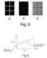
- FIG. 5shows one advantageous example of the electrode patterns for the fourth embodiment of the housing of the present invention.
- FIG. 6shows a typical signal vs. force chart
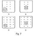
- FIG. 7shows various deflection contour maps with same level of force and contact area.
- a capacitance sensing electrodecan be used in conjunction with a metalized or metal housing that deflects under applied force. Since the amount of deflection is very small, on the order of about 0.001 of an inch, conventional electronic device housing can be converted to incorporate a user input zone using the fact that many of these types of housings are typically made from a polymer material and are plated with a conductive metal already present for electro-magnetic emissions and susceptibility requirements. Another more recent trend is to use metal as the housing structure. When this housing is connected to the ground reference of a circuit that measures capacitance, a deflection of the housing relative to the capacitance electrode can form a basis for a user input device.
- FIG. 1shows a first preferred embodiment of the invention where the deformable contact force-sensitive zone of the electronic housing 110 is shown suspended by a linear support means protruding therefrom such as a ridge 112 at an offset distance from the rigid non-deformable base 120 forming a gap.
- the design of the linear support meanscan outline a predetermined selection and size of buttons and switches for each particular application as needed.
- the first conductive layer 116is formed on the inside surface of the housing.
- the inside surface 116 of the contact force-sensitive user input housing zone 110can be metalized, printed, vacuum-deposited, sprayed or painted with a conductive material if the housing isn't made entirely from a conductive material such as metal in the first place.
- the electrode of the second conductive layer 122can be formed by printed circuit board 120 etching method or by printing a conductive paint over a rigid base 120 . Since the first conductive layer is separated from the second conductive layer with a predefined gap distance, a capacitance sensor is therefore formed therebetween and incorporated into the housing itself.
- the user input zone of the housing bodycontains the housing sections between the linear support means which are all made relatively thin and deformable under pressure.
- the housingWhen a user applies force on that section, the housing deflects down proportionally to the force applied as shown from the normal undeflected state indicated by a pair of dashed lines 114 .
- This deflectionchanges the capacitance between the two conductive layers, which can be measured by the above described circuit and interpreted as an input signal for the electronic device at a particular location on the housing.
- the degree of deflectioncan also be detected by the same circuit such that the input device can detect the level of force applied to the housing.
- Various dielectric compressible structurescan be placed optionally between the two conductive layers to fill the air gap and to form a more comprehensive capacitance sensor.
- FIG. 2shows a second embodiment of the invention where the electronic housing 210 has a contact force-sensitive deformable zone made sufficiently thin such that when a user applies force over that zone, the housing deflects as shown from the normal undeflected state indicated by a pair of dashed lines 214 .
- the capacitance sensoris formed between the inside conductive surface 216 of the housing 210 (first conductive layer) and the second conductive layer 222 of the rigid base 220 .
- the thin housingcould be made from plastic or metal and is supported by a linear support means such as columns 224 with an air gap separating it from the rigid base 220 .
- linear support meansare incorporated into the rigid base 220 as opposed to being a part of the housing 210 .
- the sections between the support meansform the buttons of the user input zone.
- the inside surface of the housing 210is metalized or painted with a conductive material if it isn't made entirely from a conductive material already. It is then connected to the ground reference of a circuit that can measure the capacitance between by the first conductive layer 216 and second conductive layer 222 .
- the second conductive layer 222can be formed by printed circuit board 220 etching method or by printing a conductive paint over the base 220 .
- the linear support meanscan be made rigid or compressible and can also be optionally made as a separate part altogether, such as for example a plurality of rubber strips. Further, more than one of such linear support means can be used together to resist deflection of the housing over a single button area (not shown).
- FIG. 3shows a third embodiment of the invention where the electronic housing 310 is suspended in a cantilever fashion away from the opening in the housing such that when a user applies force on a user input zone 310 , the housing deflects as shown from the nominal non-compressed state indicated by dashed lines 314 .
- the thin housingcould be made from plastic or metal.
- This embodimentshows an element 330 protruding from the rigid base 320 through the opening in the housing 310 .
- This elementmay be a display module, a high resolution input device or may serve other function for the electronic device.
- the inside surface of the housing 310is again metalized or painted with a conductive material if it isn't made from a conductive material and connected to the ground reference of a circuit that can measure the capacitance formed by 316 and electrode 322 .
- the electrode 322can be formed by printed circuit board 320 etching method or by printing a conductive paint over a base 320 .
- Optional linear supporting meanscan be used to support certain regions of the touch-sensitive zone of the housing (not shown) as may be dictated by the outline of the user input buttons.
- Metal sheetscan be used to form the housing of the electronic device. Finite Element Analysis has indicated that for the best performance of this invention, the range of stainless steel sheet thickness usable to construct the housing is between 0.001 and 0.007 of an inch, preferably about 0.004-0.005 of an inch. For aluminum, this range is about 0.001 to 0.012 of an inch, and preferably about 0.006 to 0.008 of an inch. For plastics, this range is broader at about 0.001 to 0.040 of an inch, with the preferred range of about 0.015 to 0.025 of an inch depending on the polymer.
- FIG. 4shows a general example of an electronic device using a housing of the present invention.
- the housing 400 of the electronic devicecomprises a bottom half 415 and the top half having a deformable contact force-sensitive user input zone 430 .
- the zone 430is made to have a conductive inside surface forming a first conductive layer.
- the rigid base 401has button-shaped electrodes 440 forming a second conductive layer and facing the inside surface of the housing 400 while spaced apart therefrom.
- a capacitance sensoris therefore formed having a number of buttons therein.
- Each button location 440is equipped with a separate electrical connection 441 connecting this location to a capacitance measuring circuit (not shown).
- the user input zone 430may have an indicia indicating the location and size of the buttons to the user (not shown).
- FIG. 5shows a fourth embodiment of the invention combining a touch-sensitive proximity sensor functionality in addition to the housing as a contact force input device. This is achieved by making the first conductive layer of the inside surface of the housing to have a mesh or some other similar non-solid pattern defining areas of its presence and absence.
- FIG. 5 ashows the button-shaped pattern of electrodes for the second conductive layer on the rigid base made for example as a printed circuit board (PCB).
- FIG. 5 bshows the corresponding traditional first conductive layer on the inside surface of the housing, which is a continuous metalized surface.
- FIG. 5 cAn example of such mesh electrode design is shown on FIG. 5 c .
- the mesh conductive layerdeflects closer to the rigid base pcb thus increasing the capacitance even further as described previously.
- the percentage of the housing acting like a proximity sensor in the areas of absence of the first electrode layer or a force sensor in the areas of its presencecan be tuned for the needs of a particular application.
- This dual mode of operationcan provide the benefits of a light touch scroll realized by a proximity touch sensor while allowing a more definitive push button selection though the housing as a second input mode of operation.
- FIG. 6shows an example of such sensor output—the first zone of input comes from proximity function and the second zone of input comes from capacitance measurement.
- FIG. 7shows two different designs of the present invention where the support structure shape is optimized to provide more uniform and localized deformation.
- panel Adue to a larger area not supported at the corners, pressing the lower left button causes a response from the adjacent upper button therefore potentially causing unwanted errors.
- panel CSimilar effects can be seen for panel B where a circular contact area created an elongated deformation due to the spacing of the support not being square.
- panel Dmaking the supports wider localized the deformation and made it more confined to the contact area while maintaining the non-square buttons typically found on cell phones.
Landscapes
- Engineering & Computer Science (AREA)
- General Engineering & Computer Science (AREA)
- Theoretical Computer Science (AREA)
- Human Computer Interaction (AREA)
- Physics & Mathematics (AREA)
- General Physics & Mathematics (AREA)
- Switches That Are Operated By Magnetic Or Electric Fields (AREA)
- Push-Button Switches (AREA)
- Switches With Compound Operations (AREA)
Abstract
Description
- Deformation-based capacitive sensors that generate a signal responsive to deformation of at least one of the conductive layers whereby causing these layers to come closer together at the location of such deformation, and
- Non-deformation based proximity sensors detecting a presence in their vicinity of a ground electrode object such as a conductive pointing device or a finger of a user—a change in capacitance is detected at a location of such ground object without any physical deformation of the sensor itself.
- Descrete button switches that at present require separate components and are only binary;
- Mechanical dome switches located under compliant skin or other flexible membranes;
- Touch pads on laptops that at present only detect contact location and not force;
- Ipod scroll wheel that at present does not detect force;
- Side keys on a phone; and
- Analog joysticks such as found on a Thinkpad Laptop
Claims (10)
Priority Applications (2)
| Application Number | Priority Date | Filing Date | Title |
|---|---|---|---|
| US12/566,768US8400402B2 (en) | 2006-04-14 | 2009-09-25 | Electronic device housing with integrated user input capability |
| PCT/US2010/050425WO2011038357A2 (en) | 2009-09-25 | 2010-09-27 | An electronic device housing with integrated user input capability |
Applications Claiming Priority (3)
| Application Number | Priority Date | Filing Date | Title |
|---|---|---|---|
| US79237906P | 2006-04-14 | 2006-04-14 | |
| US11/697,026US7595788B2 (en) | 2006-04-14 | 2007-04-05 | Electronic device housing with integrated user input capability |
| US12/566,768US8400402B2 (en) | 2006-04-14 | 2009-09-25 | Electronic device housing with integrated user input capability |
Related Parent Applications (1)
| Application Number | Title | Priority Date | Filing Date |
|---|---|---|---|
| US11/697,026Continuation-In-PartUS7595788B2 (en) | 2006-04-14 | 2007-04-05 | Electronic device housing with integrated user input capability |
Publications (2)
| Publication Number | Publication Date |
|---|---|
| US20100013775A1 US20100013775A1 (en) | 2010-01-21 |
| US8400402B2true US8400402B2 (en) | 2013-03-19 |
Family
ID=43796521
Family Applications (1)
| Application Number | Title | Priority Date | Filing Date |
|---|---|---|---|
| US12/566,768Expired - Fee RelatedUS8400402B2 (en) | 2006-04-14 | 2009-09-25 | Electronic device housing with integrated user input capability |
Country Status (2)
| Country | Link |
|---|---|
| US (1) | US8400402B2 (en) |
| WO (1) | WO2011038357A2 (en) |
Cited By (33)
| Publication number | Priority date | Publication date | Assignee | Title |
|---|---|---|---|---|
| US8547339B2 (en) | 2008-01-04 | 2013-10-01 | Tactus Technology, Inc. | System and methods for raised touch screens |
| US8553005B2 (en) | 2008-01-04 | 2013-10-08 | Tactus Technology, Inc. | User interface system |
| US8570295B2 (en) | 2008-01-04 | 2013-10-29 | Tactus Technology, Inc. | User interface system |
| US8587548B2 (en) | 2009-07-03 | 2013-11-19 | Tactus Technology, Inc. | Method for adjusting the user interface of a device |
| US8619035B2 (en) | 2010-02-10 | 2013-12-31 | Tactus Technology, Inc. | Method for assisting user input to a device |
| US8922510B2 (en) | 2008-01-04 | 2014-12-30 | Tactus Technology, Inc. | User interface system |
| US8922502B2 (en) | 2008-01-04 | 2014-12-30 | Tactus Technology, Inc. | User interface system |
| US8922503B2 (en) | 2008-01-04 | 2014-12-30 | Tactus Technology, Inc. | User interface system |
| US8928621B2 (en) | 2008-01-04 | 2015-01-06 | Tactus Technology, Inc. | User interface system and method |
| US8947383B2 (en) | 2008-01-04 | 2015-02-03 | Tactus Technology, Inc. | User interface system and method |
| US8970403B2 (en) | 2008-01-04 | 2015-03-03 | Tactus Technology, Inc. | Method for actuating a tactile interface layer |
| US9019228B2 (en) | 2008-01-04 | 2015-04-28 | Tactus Technology, Inc. | User interface system |
| US9052790B2 (en) | 2008-01-04 | 2015-06-09 | Tactus Technology, Inc. | User interface and methods |
| US9063627B2 (en) | 2008-01-04 | 2015-06-23 | Tactus Technology, Inc. | User interface and methods |
| US9075525B2 (en) | 2008-01-04 | 2015-07-07 | Tactus Technology, Inc. | User interface system |
| US9098141B2 (en) | 2008-01-04 | 2015-08-04 | Tactus Technology, Inc. | User interface system |
| US9116617B2 (en) | 2009-07-03 | 2015-08-25 | Tactus Technology, Inc. | User interface enhancement system |
| US9239623B2 (en) | 2010-01-05 | 2016-01-19 | Tactus Technology, Inc. | Dynamic tactile interface |
| US9274612B2 (en) | 2008-01-04 | 2016-03-01 | Tactus Technology, Inc. | User interface system |
| US9280224B2 (en) | 2012-09-24 | 2016-03-08 | Tactus Technology, Inc. | Dynamic tactile interface and methods |
| US9298261B2 (en) | 2008-01-04 | 2016-03-29 | Tactus Technology, Inc. | Method for actuating a tactile interface layer |
| US9372565B2 (en) | 2008-01-04 | 2016-06-21 | Tactus Technology, Inc. | Dynamic tactile interface |
| US9405417B2 (en) | 2012-09-24 | 2016-08-02 | Tactus Technology, Inc. | Dynamic tactile interface and methods |
| US9423875B2 (en) | 2008-01-04 | 2016-08-23 | Tactus Technology, Inc. | Dynamic tactile interface with exhibiting optical dispersion characteristics |
| US9477308B2 (en) | 2008-01-04 | 2016-10-25 | Tactus Technology, Inc. | User interface system |
| US9552065B2 (en) | 2008-01-04 | 2017-01-24 | Tactus Technology, Inc. | Dynamic tactile interface |
| US9557915B2 (en) | 2008-01-04 | 2017-01-31 | Tactus Technology, Inc. | Dynamic tactile interface |
| US9557813B2 (en) | 2013-06-28 | 2017-01-31 | Tactus Technology, Inc. | Method for reducing perceived optical distortion |
| US9588683B2 (en) | 2008-01-04 | 2017-03-07 | Tactus Technology, Inc. | Dynamic tactile interface |
| US9588684B2 (en) | 2009-01-05 | 2017-03-07 | Tactus Technology, Inc. | Tactile interface for a computing device |
| US9612659B2 (en) | 2008-01-04 | 2017-04-04 | Tactus Technology, Inc. | User interface system |
| US9720501B2 (en) | 2008-01-04 | 2017-08-01 | Tactus Technology, Inc. | Dynamic tactile interface |
| US9760172B2 (en) | 2008-01-04 | 2017-09-12 | Tactus Technology, Inc. | Dynamic tactile interface |
Families Citing this family (26)
| Publication number | Priority date | Publication date | Assignee | Title |
|---|---|---|---|---|
| US8136402B2 (en)* | 2007-11-28 | 2012-03-20 | International Business Machines Corporation | Accelerometer module for use with a touch sensitive device |
| US8284170B2 (en)* | 2008-09-30 | 2012-10-09 | Apple Inc. | Touch screen device, method, and graphical user interface for moving on-screen objects without using a cursor |
| US8872771B2 (en)* | 2009-07-07 | 2014-10-28 | Apple Inc. | Touch sensing device having conductive nodes |
| US9632622B2 (en)* | 2009-07-16 | 2017-04-25 | Apple Inc. | Ground detection for touch sensitive device |
| US8780537B2 (en) | 2010-05-07 | 2014-07-15 | Tyco Electronics Corporation | Integrated connection system for an electronic device |
| EP2395414B1 (en)* | 2010-06-11 | 2014-08-13 | BlackBerry Limited | Portable electronic device including touch-sensitive display and method of changing tactile feedback |
| US8351993B2 (en) | 2010-10-08 | 2013-01-08 | Research In Motion Limited | Device having side sensor |
| CA2849432A1 (en)* | 2010-10-20 | 2012-04-26 | Yota Devices Ipr Ltd | Mobile device |
| US9569002B2 (en) | 2010-12-17 | 2017-02-14 | Blackberry Limited | Portable electronic device having a sensor arrangement for gesture recognition |
| WO2013068791A1 (en)* | 2011-11-11 | 2013-05-16 | Nokia Corporation | User interface method and apparatus for providing deformation-sensitive input |
| US9405319B2 (en)* | 2011-12-16 | 2016-08-02 | Nokia Technologies Oy | Casing |
| WO2013123310A1 (en) | 2012-02-15 | 2013-08-22 | Intuitive Surgical Operations, Inc. | User selection of robotic system operating modes using mode distinguishing operator actions |
| US20140085217A1 (en)* | 2012-09-27 | 2014-03-27 | Htc Corporation | Electronic apparatus and control method thereof |
| US9285889B2 (en)* | 2012-12-10 | 2016-03-15 | Intel Corporation | Electrode arrangement for a keyboard proximity and tracking sensor |
| KR102043370B1 (en)* | 2012-12-18 | 2019-11-13 | 삼성디스플레이 주식회사 | controlling method of user input using pressure sensor unit for flexible display device |
| JP6086380B2 (en)* | 2013-01-15 | 2017-03-01 | Nltテクノロジー株式会社 | Touch panel and display device having touch panel |
| US10743620B2 (en) | 2015-05-28 | 2020-08-18 | Nike, Inc. | Automated tensioning system for an article of footwear |
| US10088906B2 (en)* | 2015-11-10 | 2018-10-02 | Joyhaptics Oy | Method and apparatus for recognizing swipe operation of a user on a user interface |
| US20170262110A1 (en)* | 2016-03-10 | 2017-09-14 | Synaptics Incorporated | Hybrid force sensor |
| US11202484B2 (en)* | 2016-03-15 | 2021-12-21 | Nike, Inc. | Standoff unit for a control device in an article of footwear |
| KR102552294B1 (en)* | 2016-07-15 | 2023-07-10 | 삼성디스플레이 주식회사 | Pressure sensor and display device including the same |
| KR102552283B1 (en) | 2016-07-15 | 2023-07-10 | 삼성디스플레이 주식회사 | Pressure sensor and display device including the same |
| GB201708210D0 (en) | 2017-05-22 | 2017-07-05 | Tangi0 Ltd | Sensor device and method |
| KR102702870B1 (en)* | 2019-08-14 | 2024-09-05 | 삼성전자주식회사 | Electronic device including opening |
| WO2021137334A1 (en)* | 2020-01-02 | 2021-07-08 | 엘지전자 주식회사 | Mobile terminal |
| US11269457B1 (en) | 2021-02-03 | 2022-03-08 | Apple Inc. | Systems and methods for improved touch screen selectivity and sensitivity |
Citations (4)
| Publication number | Priority date | Publication date | Assignee | Title |
|---|---|---|---|---|
| US4224615A (en)* | 1978-09-14 | 1980-09-23 | Texas Instruments Incorporated | Method of using a liquid crystal display device as a data input device |
| US20030234769A1 (en)* | 2002-06-25 | 2003-12-25 | Cross Elisa M. | Touch sensor |
| US20060197750A1 (en)* | 2005-03-04 | 2006-09-07 | Apple Computer, Inc. | Hand held electronic device with multiple touch sensing devices |
| US20060274042A1 (en)* | 2005-06-03 | 2006-12-07 | Apple Computer, Inc. | Mouse with improved input mechanisms |
Family Cites Families (3)
| Publication number | Priority date | Publication date | Assignee | Title |
|---|---|---|---|---|
| JP3827875B2 (en)* | 1999-01-27 | 2006-09-27 | アルプス電気株式会社 | Membrane switch |
| US7046230B2 (en)* | 2001-10-22 | 2006-05-16 | Apple Computer, Inc. | Touch pad handheld device |
| US6600120B1 (en)* | 2002-07-01 | 2003-07-29 | Koninklijke Philips Electronics N.V. | Membrane switch arrangement with chamber venting |
- 2009
- 2009-09-25USUS12/566,768patent/US8400402B2/ennot_activeExpired - Fee Related
- 2010
- 2010-09-27WOPCT/US2010/050425patent/WO2011038357A2/enactiveApplication Filing
Patent Citations (4)
| Publication number | Priority date | Publication date | Assignee | Title |
|---|---|---|---|---|
| US4224615A (en)* | 1978-09-14 | 1980-09-23 | Texas Instruments Incorporated | Method of using a liquid crystal display device as a data input device |
| US20030234769A1 (en)* | 2002-06-25 | 2003-12-25 | Cross Elisa M. | Touch sensor |
| US20060197750A1 (en)* | 2005-03-04 | 2006-09-07 | Apple Computer, Inc. | Hand held electronic device with multiple touch sensing devices |
| US20060274042A1 (en)* | 2005-06-03 | 2006-12-07 | Apple Computer, Inc. | Mouse with improved input mechanisms |
Cited By (45)
| Publication number | Priority date | Publication date | Assignee | Title |
|---|---|---|---|---|
| US9274612B2 (en) | 2008-01-04 | 2016-03-01 | Tactus Technology, Inc. | User interface system |
| US9063627B2 (en) | 2008-01-04 | 2015-06-23 | Tactus Technology, Inc. | User interface and methods |
| US8570295B2 (en) | 2008-01-04 | 2013-10-29 | Tactus Technology, Inc. | User interface system |
| US9760172B2 (en) | 2008-01-04 | 2017-09-12 | Tactus Technology, Inc. | Dynamic tactile interface |
| US9720501B2 (en) | 2008-01-04 | 2017-08-01 | Tactus Technology, Inc. | Dynamic tactile interface |
| US8717326B2 (en) | 2008-01-04 | 2014-05-06 | Tactus Technology, Inc. | System and methods for raised touch screens |
| US8922510B2 (en) | 2008-01-04 | 2014-12-30 | Tactus Technology, Inc. | User interface system |
| US8922502B2 (en) | 2008-01-04 | 2014-12-30 | Tactus Technology, Inc. | User interface system |
| US8922503B2 (en) | 2008-01-04 | 2014-12-30 | Tactus Technology, Inc. | User interface system |
| US8928621B2 (en) | 2008-01-04 | 2015-01-06 | Tactus Technology, Inc. | User interface system and method |
| US8947383B2 (en) | 2008-01-04 | 2015-02-03 | Tactus Technology, Inc. | User interface system and method |
| US8970403B2 (en) | 2008-01-04 | 2015-03-03 | Tactus Technology, Inc. | Method for actuating a tactile interface layer |
| US9019228B2 (en) | 2008-01-04 | 2015-04-28 | Tactus Technology, Inc. | User interface system |
| US9626059B2 (en) | 2008-01-04 | 2017-04-18 | Tactus Technology, Inc. | User interface system |
| US9052790B2 (en) | 2008-01-04 | 2015-06-09 | Tactus Technology, Inc. | User interface and methods |
| US9619030B2 (en) | 2008-01-04 | 2017-04-11 | Tactus Technology, Inc. | User interface system and method |
| US9075525B2 (en) | 2008-01-04 | 2015-07-07 | Tactus Technology, Inc. | User interface system |
| US9098141B2 (en) | 2008-01-04 | 2015-08-04 | Tactus Technology, Inc. | User interface system |
| US9612659B2 (en) | 2008-01-04 | 2017-04-04 | Tactus Technology, Inc. | User interface system |
| US9207795B2 (en) | 2008-01-04 | 2015-12-08 | Tactus Technology, Inc. | User interface system |
| US9229571B2 (en) | 2008-01-04 | 2016-01-05 | Tactus Technology, Inc. | Method for adjusting the user interface of a device |
| US9588683B2 (en) | 2008-01-04 | 2017-03-07 | Tactus Technology, Inc. | Dynamic tactile interface |
| US8553005B2 (en) | 2008-01-04 | 2013-10-08 | Tactus Technology, Inc. | User interface system |
| US8547339B2 (en) | 2008-01-04 | 2013-10-01 | Tactus Technology, Inc. | System and methods for raised touch screens |
| US9035898B2 (en) | 2008-01-04 | 2015-05-19 | Tactus Technology, Inc. | System and methods for raised touch screens |
| US9298261B2 (en) | 2008-01-04 | 2016-03-29 | Tactus Technology, Inc. | Method for actuating a tactile interface layer |
| US9372565B2 (en) | 2008-01-04 | 2016-06-21 | Tactus Technology, Inc. | Dynamic tactile interface |
| US9372539B2 (en) | 2008-01-04 | 2016-06-21 | Tactus Technology, Inc. | Method for actuating a tactile interface layer |
| US9557915B2 (en) | 2008-01-04 | 2017-01-31 | Tactus Technology, Inc. | Dynamic tactile interface |
| US9423875B2 (en) | 2008-01-04 | 2016-08-23 | Tactus Technology, Inc. | Dynamic tactile interface with exhibiting optical dispersion characteristics |
| US9430074B2 (en) | 2008-01-04 | 2016-08-30 | Tactus Technology, Inc. | Dynamic tactile interface |
| US9448630B2 (en) | 2008-01-04 | 2016-09-20 | Tactus Technology, Inc. | Method for actuating a tactile interface layer |
| US9477308B2 (en) | 2008-01-04 | 2016-10-25 | Tactus Technology, Inc. | User interface system |
| US9495055B2 (en) | 2008-01-04 | 2016-11-15 | Tactus Technology, Inc. | User interface and methods |
| US9524025B2 (en) | 2008-01-04 | 2016-12-20 | Tactus Technology, Inc. | User interface system and method |
| US9552065B2 (en) | 2008-01-04 | 2017-01-24 | Tactus Technology, Inc. | Dynamic tactile interface |
| US9588684B2 (en) | 2009-01-05 | 2017-03-07 | Tactus Technology, Inc. | Tactile interface for a computing device |
| US9116617B2 (en) | 2009-07-03 | 2015-08-25 | Tactus Technology, Inc. | User interface enhancement system |
| US8587548B2 (en) | 2009-07-03 | 2013-11-19 | Tactus Technology, Inc. | Method for adjusting the user interface of a device |
| US9239623B2 (en) | 2010-01-05 | 2016-01-19 | Tactus Technology, Inc. | Dynamic tactile interface |
| US9298262B2 (en) | 2010-01-05 | 2016-03-29 | Tactus Technology, Inc. | Dynamic tactile interface |
| US8619035B2 (en) | 2010-02-10 | 2013-12-31 | Tactus Technology, Inc. | Method for assisting user input to a device |
| US9405417B2 (en) | 2012-09-24 | 2016-08-02 | Tactus Technology, Inc. | Dynamic tactile interface and methods |
| US9280224B2 (en) | 2012-09-24 | 2016-03-08 | Tactus Technology, Inc. | Dynamic tactile interface and methods |
| US9557813B2 (en) | 2013-06-28 | 2017-01-31 | Tactus Technology, Inc. | Method for reducing perceived optical distortion |
Also Published As
| Publication number | Publication date |
|---|---|
| WO2011038357A2 (en) | 2011-03-31 |
| WO2011038357A3 (en) | 2011-08-18 |
| US20100013775A1 (en) | 2010-01-21 |
Similar Documents
| Publication | Publication Date | Title |
|---|---|---|
| US8400402B2 (en) | Electronic device housing with integrated user input capability | |
| US7595788B2 (en) | Electronic device housing with integrated user input capability | |
| US9069426B2 (en) | Sensing capacitance changes of a housing of an electronic device | |
| US5942733A (en) | Stylus input capacitive touchpad sensor | |
| US20230015526A1 (en) | Keyless keyboard with force sensing and haptic feedback | |
| EP2307947B1 (en) | Single sided capacitive force sensor for electronic devices | |
| CN114741007B (en) | Input device with force sensor | |
| JP5611282B2 (en) | Force imaging input devices and systems | |
| KR102014561B1 (en) | Touch sensitive film, touch sensing device, and electronic device | |
| US6943705B1 (en) | Method and apparatus for providing an integrated membrane switch and capacitive sensor | |
| US6002389A (en) | Touch and pressure sensing method and apparatus | |
| US10353485B1 (en) | Multifunction input device with an embedded capacitive sensing layer | |
| US7609178B2 (en) | Reconfigurable tactile sensor input device | |
| US20130093681A1 (en) | Capacitive touch key panel | |
| JP2012529126A (en) | Input device and method with pressure sensitive layer | |
| KR20100022747A (en) | Touch sensor comprising piezorisistive layer and input device comprising the same, and input detection method thereof | |
| KR20130103254A (en) | The touch screen and key which can measure the coordinate and strength of touch position by deflection or viration sensors | |
| KR100932428B1 (en) | touch screen using the tactile sensor and method for manufacturing the same | |
| KR102550768B1 (en) | Integrated system comprising capacity sensor and vibration actuator based on magnetorheological elastomer | |
| KR20150085396A (en) | Complex-type input device with touch sensing features | |
| CN222562014U (en) | Capacitive sensing track pad with force sensing and tactile features | |
| US10761622B2 (en) | Pressure sensing on a touch sensor using capacitance | |
| KR101673135B1 (en) | Digitizer system | |
| HK1197842A (en) | Touch sensitive film, touch sensing device, and electronic device |
Legal Events
| Date | Code | Title | Description |
|---|---|---|---|
| AS | Assignment | Owner name:PRESSURE PROFILE SYSTEMS, INC.,CALIFORNIA Free format text:ASSIGNMENT OF ASSIGNORS INTEREST;ASSIGNOR:SON, JAE S;REEL/FRAME:023295/0388 Effective date:20090924 Owner name:PRESSURE PROFILE SYSTEMS, INC., CALIFORNIA Free format text:ASSIGNMENT OF ASSIGNORS INTEREST;ASSIGNOR:SON, JAE S;REEL/FRAME:023295/0388 Effective date:20090924 | |
| STCF | Information on status: patent grant | Free format text:PATENTED CASE | |
| FPAY | Fee payment | Year of fee payment:4 | |
| AS | Assignment | Owner name:WISETOUCH CO, LTD, KOREA, REPUBLIC OF Free format text:ASSIGNMENT OF ASSIGNORS INTEREST;ASSIGNOR:PRESSURE PROFILE SYSTEMS INC.;REEL/FRAME:041537/0511 Effective date:20170123 | |
| MAFP | Maintenance fee payment | Free format text:PAYMENT OF MAINTENANCE FEE, 8TH YR, SMALL ENTITY (ORIGINAL EVENT CODE: M2552); ENTITY STATUS OF PATENT OWNER: SMALL ENTITY Year of fee payment:8 | |
| FEPP | Fee payment procedure | Free format text:MAINTENANCE FEE REMINDER MAILED (ORIGINAL EVENT CODE: REM.); ENTITY STATUS OF PATENT OWNER: SMALL ENTITY | |
| LAPS | Lapse for failure to pay maintenance fees | Free format text:PATENT EXPIRED FOR FAILURE TO PAY MAINTENANCE FEES (ORIGINAL EVENT CODE: EXP.); ENTITY STATUS OF PATENT OWNER: SMALL ENTITY | |
| STCH | Information on status: patent discontinuation | Free format text:PATENT EXPIRED DUE TO NONPAYMENT OF MAINTENANCE FEES UNDER 37 CFR 1.362 | |
| FP | Lapsed due to failure to pay maintenance fee | Effective date:20250319 |