US8397043B2 - Memory mapping system, request controller, multi-processing arrangement, central interrupt request controller, apparatus, method for controlling memory access and computer program product - Google Patents
Memory mapping system, request controller, multi-processing arrangement, central interrupt request controller, apparatus, method for controlling memory access and computer program productDownload PDFInfo
- Publication number
- US8397043B2 US8397043B2US12/808,382US80838210AUS8397043B2US 8397043 B2US8397043 B2US 8397043B2US 80838210 AUS80838210 AUS 80838210AUS 8397043 B2US8397043 B2US 8397043B2
- Authority
- US
- United States
- Prior art keywords
- memory
- processing unit
- memory section
- write access
- processing
- Prior art date
- Legal status (The legal status is an assumption and is not a legal conclusion. Google has not performed a legal analysis and makes no representation as to the accuracy of the status listed.)
- Expired - Fee Related, expires
Links
Images


Classifications
- G—PHYSICS
- G06—COMPUTING OR CALCULATING; COUNTING
- G06F—ELECTRIC DIGITAL DATA PROCESSING
- G06F12/00—Accessing, addressing or allocating within memory systems or architectures
- G06F12/02—Addressing or allocation; Relocation
- G06F12/0223—User address space allocation, e.g. contiguous or non contiguous base addressing
- G06F12/0284—Multiple user address space allocation, e.g. using different base addresses
- G—PHYSICS
- G06—COMPUTING OR CALCULATING; COUNTING
- G06F—ELECTRIC DIGITAL DATA PROCESSING
- G06F12/00—Accessing, addressing or allocating within memory systems or architectures
- G06F12/14—Protection against unauthorised use of memory or access to memory
- G06F12/1416—Protection against unauthorised use of memory or access to memory by checking the object accessibility, e.g. type of access defined by the memory independently of subject rights
Definitions
- This inventionrelates to a memory mapping system, to a request controller, to a multi-processing arrangement, to a Central Interrupt Request Controller, to an apparatus, to a method for controlling memory access and to a computer program product.
- Multi-processing arrangementsare known in the art.
- microprocessors and microcontrollerswhich include two or more processing cores.
- Such microprocessors and microcontrollersare referred to in the art as multi-core processors.
- multi-processing arrangementsrequire optimization of other components such as, in the case of multi-core processors the interrupt controller and the memory. Different methods have been disclosed in the art to optimize interrupt controllers for multi-core processors.
- WO 97/44738discloses a multi-processing computer system which includes an interrupt controller coupled to an expansion bus.
- the programmable interrupt controllerhas multiple storage locations at the same address for multiple central processing units or CPUs.
- the CPUsare coupled to a host bus which in turn is coupled to the expansion bus by means of a bus bridge.
- An arbiteris coupled to the host bus for arbitrating bus mastership amongst the CPUs.
- CPU host owner identificationis transferred across the bus bridge to the programmable interrupt controller.
- the programmable interrupt controlleruses the CPU host owner identification to determine which storage location is to be accessed.
- the present inventionprovides a memory mapping system, a request controller, a multi-processing arrangement, an apparatus, a method for controlling memory access and a computer program product as described in the accompanying claims.
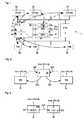
- FIG. 1shows a block diagram of an example of an embodiment of a multi-processing arrangement
- FIG. 2shows an example of an embodiment of a memory mapping system suitable for the example of FIG. 1 ;
- FIG. 3illustrates a write access to the example of FIG. 2 ;
- FIGS. 4-7illustrate handling of different types of interrupt requests involving a multiple of processing units of the example of FIG. 1
- FIG. 8shows a block diagram of an access protection unit suitable for the peripheral bridge of the example of FIG. 1 .
- FIG. 9schematically shows an example of an embodiment of an apparatus including a multi-processing arrangement.
- the example of a multi-processing arrangement 1 shown thereinincludes a plurality of processing units 2 a - 2 n .
- the multi-processing arrangement 1may include any suitable number of processing units.
- the multiprocessor system 1may for example include two or more, such as three or more, such as four or more processing units.
- the multi-processing arrangement 1may for example be implemented as single package composed of a single die, or of two or more dies packaged together.
- multi-processing arrangement 1may include a request controller 3 .
- the request controller 3may include a memory mapping system 30 .
- the shown memory mapping system 30is connected to the processing units 2 a - 2 n .
- the memory mapping system 30may be provided as a separate component which can be connected to the multi-processing arrangement 1 .
- the memory mapping system 30may include a main memory.
- the main memorymay include a first memory section 31 and a second memory section 32 .
- one or more processing units 2 a - 2 nmay be designated first processing unit, which have write access to the main memory.
- One or more processing units 2 a - 2 nmay be designated second processing unit(s), which do not have write access to the main memory.
- the memory mapping system 30may include one or more associated memories 9 a - 9 m , which are associated with the second memory section 32 .
- the associated memories 9 a - 9 mmay each include a memory section to which a respective one of the second processing units has write access.
- the memory mapping system 30may include a consistency control unit 33 .
- the consistency control unit 33may maintain consistency between data stored in the associated memory 9 a - 9 m and the second memory section 32 .
- the first memory section 31is protected against inadvertent modification by a respective second processing unit. Accordingly, in the first memory section 31 data may be stored which has to be protected, such as configuration data of the multi-processing arrangement 1 or other critical data.
- the data in the first memory section 31may for example be stored before operation, and for example be protected from writing by any of the processing units.
- the first processing unitmay have write access to at least the first memory section of the main memory.
- the information in the second memory section 32 and the associated memory 9 a - 9 mremains consistent, thereby enabling usage by the first processing unit of data stored in the associated memory 9 a - 9 m and enabling usage by the second processing unit of data stored in the second memory section.
- critical datamay be protected in a simple manner whereas non-critical data can be shared and/or exchanged and/or used by both the first and second processing units in a relatively simple manner.
- the memory mapping system 30may be implemented in any manner suitable for the specific implementation.
- the number of the associated memoriesmay for instance correspond to the number of the processing units.
- the memory mapping system 30may include two or more associated memories, to each of which a respective second processing unit has write access and to which the other processing units in the multi-processing arrangement 1 do not have write access.
- the main memory 30 and the associated memories 9 a - 9 mmay for example both be part of a memory of the request controller 3 and/or of the multi-processing arrangement 1 .
- the request controller 3may include a set of registers. which may be split up in a number of register sets, such as a set A which forms the first memory section 31 , a set B which forms the section memory section 32 and a respective set M# 1 -M#m for each associated memory 9 a - 9 m .
- the register set which forms the first memory section 31may for example contain configuration registers of the controller 3 which are to stay unmodified during the handling of a request, e.g. during the execution of an interrupt by one or more of the processing units 2 a - 2 n .
- the register set which forms the second memory section 32may include registers which are allowed to be modified during the handling of a request without affecting the operation of the arrangement of which the memory mapping systems forms a part.
- the second memory sectionmay include registers which contain status information about the handling of a request, which may be updated by a respective processing unit.
- the associated memories 9 a - 9 mmay for example be implemented in the memory of the request controller 3 by allocating to each associated memory 9 a - 9 m a set of registers M# 1 -M#m. For each set M# 1 -M#m, for example write access may be set per bit location, and for example only those bit locations may be released which are allowed to be modified by the corresponding processing unit.
- a configuration fielde.g. a bit, in register set A may be used to determine whether a processing unit is allowed to write in the set B and/or in the sets M# 1 -M#m.
- the access rights to register set B and to the sets M# 1 -M#mwill correspond to the settings of the configuration field. If a processing unit is not allowed to make access to a respective associated memory, its write accesses to register set B may be blocked.
- the configuration bits and the access rightsmay for example be set such that only the processing unit with the highest safety level has write access to the register sets A and B, while every other processing unit only has write access to a respective associated memory 9 a - 9 m.
- the second memory section 32 and the associated memor(y)(ies) 9 a - 9 mmay be spaced apart.
- the distance between the second memory section and the associated memorymay exceed a granularity of a memory protection scheme, e.g. as used by a memory management unit or a memory protection unit, thereby obviating the need to provide a memory protection scheme with a finer granularity.
- the memory protection schememay provide protection at a byte level (that is: write control and/or read control may be set per byte of data) and second memory section 32 and the associated memories 9 a - 9 m may have no overlap in bytes.
- the memory section 32 and the associated memory 9 a - 9 mmay for example be assigned different address ranges of a memory, between which there is a spacing which is at least as large as the granularity of the protection scheme.
- the main and/or associated memorymay be on-chip memory and include a number of registers with a certain size, for example X bits.
- the memorymay for example be provided with an access control mechanism which allows read and/or write access to be set per register.
- the main memorymay use different registers than the associated memory, without any overlap in registers.
- the main memorymay use a register set and the associated memories 9 a - 9 m may use respective registers sets which do not overlap with the main memory.
- the consistency control unit 33may include synchronization paths 201 - 203 between the second memory section 32 and the associated memories 9 i , 9 j . Via the synchronization paths 201 - 203 , data consistency between second memory section 32 and the associated memories may be maintained. For instance, if a processing unit changes e.g. bit locations of a register in the associated memory 9 i , the corresponding bit locations may be updated by way of the signal path 202 in the part (e.g. the register) of the second memory section 32 which are associated with the respective part in the associated memory 9 i .
- Signal path 200allows updating bit locations in the associated memory 9 i after the first processing unit (CPU #y) has written corresponding bit locations in the second memory section 32 . As shown with the updating paths 201 and 203 , for other register associated memory 9 i a similar function may be present.
- a processing unitmay for example terminate the execution of an interrupt routine with a write access to an EOI (End of Interrupt) register.
- EOIEnd of Interrupt
- a second processing unitCPU #x
- CPU #xmay write an interrupt complete notification into an associated EOI register (M-EOI) 90 i in the associated memory 9 i .
- M-EOIassociated EOI register
- an EOI register 320may be present which is associated with the M-EOI 90 i .
- the content of the EOI register 320may then be updated via a signal path 202 ′ which connects the MEOI 90 i and the EOI 320 .
- the end of the execution of the interrupt service routinebecomes effective and all processing units can read in the respective memory that the interrupt has been handled.
- any data suitable for the specific implementationmay be stored.
- the first memory sectionmay for example contain configuration data and the first processing unit may have exclusive write access to the first memory section.
- the second memory section and the associated memorymay for example both include a request handling memory in which data about a handling of requests is stored. Referring to FIGS. 4-7 examples of embodiments which are capable of inter-processor request handing are shown.
- the memory mapping systemmay be used for inter processor interrupt (IPI) handling, e.g. for interrupts generated by a processing unit which are to be handled by another processing unit in the multiprocessing unit.
- IPIinter processor interrupt
- the first processing unit(CPU #y in those examples) may have write access to a part (xset 0 . . . x-set 5 ) of the second memory section 32 associated with blocked memory section ( 92 , 92 ′)s (Mxset 0 . . . Mx-set 5 ) in an associated memory 9 i , in order to store, for example, request demand messages.
- the second processing unitthen may have write access to an un-blocked part (e.g. Mx-clr 0 . . . MX-Clr 5 ) of the associated memory 9 i in order to store request handled messages.
- the first processing unitcan ask the second processing unit to execute a certain request, e.g. to execute a software routine, and the second processing unit can notify the first processing unit about the status of the request (e.g. that the request is handled).
- the processing unit CPU #yhas the highest priority and is designated first processing unit. Accordingly, CPU #y has exclusive write access to the second memory section B, while the other processing units CPU #x (and in FIG. 7 CPU #z) have write access to the respective associated memories 9 i , 9 j and not to the second memory section B.
- sets of two bits 92 , 93 ; 92 ′; 93 ′; 321 , 322 ; 321 ′, 322 ′(indicated with set and clr respectively in the figures) or other types of field may be provided for the same IPI in both the associated memor(y)(ies) 9 i and the second memory section 32 .
- the CPU #ymay request an interrupt of the CPU #x by writing e.g. one of the two dedicated bits x_SET 0 321 or x_SET 1 321 ′ in the IPI memory 32 .
- the CPU #xAfter the execution of the interrupt service routine, the CPU #x writes on the corresponding bit Mx_CLR 0 92 or Mx_CLR 1 92 ′ in the IPI associated memory 320 .
- the changes of the bits Mx_CLR 0 and Mx_CLR 1are transmitted to the bits x_CLR 0 and x_CLR 1 through the signal paths 204 and 204 ′.
- the software running on the second processing unit CPU #xmay request an interrupt of the processors by writing e.g. one of the two dedicated bits Mx_SET 2 94 or Mx_SET 3 94 ′ in the IPI associated memory 91 .
- the value of the changed bit Mx_SET 2 or Mx_SET 3is transmitted via a respective signal path 205 , 205 ′ for registration in the bit location x_SET 2 323 or x_SET 3 323 ′ of the IPI memory 320 .
- the interrupt requestis then activated in the system based on the IPI memory 320 .
- the CPU #xmay write on the corresponding bit Mx_CLR 2 95 or Mx_CLR 3 95 ′ in the IPI associated memory 91 .
- the changes to the bits Mx_CLR 2 and Mx_CLR 3may then be transferred to the bits x_CLR 2 and x_CLR 3 via the signal paths 206 and 206 ′.
- the second processing unit CPU #xmay request an interrupt of the first processing unit CPU #y by describing e.g. one of the two dedicated bits Mx_SET 4 96 or Mx_SET 5 96 ′ in the associated IPI (Inter-Processor Interrupt) memory 91 .
- Bit x_SET 4 96 or x_SET 5 96 ′may be set in the IPI memory 91 via path 207 , 207 ′.
- the CPU #ymay reset the corresponding bit x_CLR 4 326 or x_CLR 5 326 ′ in the IPI memory 320 .
- the reset valueis registered in the associated IPI (Inter-Processor Interrupt) memory by way of signal path 208 , 208 ′.
- the processing unit CPU #zmay adopt an interrupt requested by the processing unit #x.
- the processing unit CPU #xmay set the bit Mxz_SET 0 98 or Mxz_SET 1 98 ′ in the IPI associated memory 91 .
- Bit xz_SET 0 96 or xz_SET 1 96 ′ in the IPI register 320may be synchronized to the set values by way of a respective signal path 209 , 209 ′. Thereafter, the processing unit CPU #z can start to execute the interrupt.
- the processing unit CPU #zmay write on the corresponding bit Nxz_CLR 0 101 or Nxz_CLR 1 101 in to the IPI associated register 91 assigned to the processing unit CPU #z. Via the signal path 211 , 211 ′, this writing may be registered in the IPI register 320 , and from there the bit value may be made visible in the associated IPI register 91 via the signal path 210 or 210 ′, e.g. by synchronizing fields Mxz-clr 0 and Mxz-clr 1 to the fields in the IPI register 320 of the second memory section 32 .
- the request controller 3may be implemented in any manner suitable for the specific implementation.
- the request controller 3may for example control a processing of requests by one or more first processing units and by one or more second processing units.
- the requestsmay for example be an interrupt request, a context switch request, a task switch request, a thread switch request, a process switch request or another suitable type of request.
- the request controllermay be arranged to control one of more of: inter processor interrupt requests, software interrupt requests, hardware interrupt requests.
- the request controlleris a central request controller (CRC).
- the CRCmay receive requests from peripheral devices in the arrangement 1 or from devices outside the arrangement 1 and control the handling of the interrupts.
- the CRCmay for example perform functions such as prioritizing requests, assigning requests to a specific processing unit for all the requests which are sent to (all) the processing units.
- the multi-processing arrangement 1may be implemented in any manner suitable for the specific implementation.
- the multi-processing arrangementmay be implemented as a single integrated circuit.
- the multi-processing arrangementmay for instance be implemented as a multi-core microprocessor or microcontroller used in a safety related application, such as, for example, a braking system, an electronic control unit, a seat belt, an air traffic control system, a fly-by-wire system, a life support system or in a central control node in a control system.
- a safety related applicationsuch as, for example, a braking system, an electronic control unit, a seat belt, an air traffic control system, a fly-by-wire system, a life support system or in a central control node in a control system.
- a safety related applicationsuch as, for example, a braking system, an electronic control unit, a seat belt, an air traffic control system, a fly-by-wire system, a life support system or in a central control node in a control system.
- a processing unitmay be designated as a main processor which may, for instance, configure the multi-processing arrangement 1 .
- At least a part of the data used by the main processore.g. the configuration data, may be protected against inadvertent modification by other processing units (which thus are second processing units for the main processor, which thus forms a first processing unit).
- the multi-processing arrangementmay for instance include a plurality of processing units of which a main safety processing unit forms the first processing unit is and a redundant processing unit forms the second processing unit.
- different safety levels(SIL1, SIL2, SIL3, or SIL4) according to IEC standard 61508 can be allocated to the processing units, with SIL4 representing the highest and SIL1 the lowest safety level.
- the safety level of a processing unitcan be increased by an internal redundancy of hardware resources, for example.
- Two processor cores, monitoring each other reciprocally within a processing unitoffer a higher rate of safety than one single processor core.
- a SIL2 processing unitcan modify data of an SIL3 processing unit in the interrupt controller 23 .
- the less safe processing unitcan impair the safety level of the safer processing unit.
- such impairmentmay be prevented or at least the risk thereof reduced.
- the selection of the main safety processing unitmay be configurable, for example by writing in a configuration part of the first memory section 31 .
- the processing unitsmay be designated first and second processing units based upon the safety level of the combination of the hardware system and software implementation on each processing unit. For instance, a processing unit with the highest safety level may be designated first processing unit for all other processing units. Also, one or more processing units with a second safety level below the highest safety level may act as a first processing unit with respect to other processing units with a safety level below the second safety level or all processing units with a safety level below the highest safety level may be designated second processing units.
- the safety levelmay for example be the Safety Integrity Level as defined by International Standard IEC 61508, with SIL 4 being the highest safety level and SIL 1 being the lowest safety level.
- the first processing unit and/or the second processing unitmay be arranged to execute a software application.
- the memory mapping systemmay be transparent for the software application.
- the software applicationmay receive interrupts, handle interrupts or generate interrupts without having to e.g. assign data to a specific one of the second memory section 32 or an associated memory.
- the arrangement 1may include a plurality of processor cores CPU# 1 -CPU#N which are connected to a Central Interrupt Request Controller (CIRC).
- CIRCCentral Interrupt Request Controller
- the processor coresare connected to the CIRC, as indicated with the dash-dotted arrows, (and each other) via a processor bus 4 .
- CIRCCentral Interrupt Request Controller
- other suitable types of connectionsmay be provided between the processor cores an the CIRC.
- peripheral units (P# 1 -P#k) 6 a - 6 kmay be present.
- the peripheral unit(s)may for example be non-core components of the multi-core processor such as inputs/outputs or other components, such as and/or communication interfaces and/or coprocessors and/or analog-to-digital converters and/or clocks and reset generation units, voltage regulators, memory (such as for instance flash, EEPROM, RAM), error correction code logic and/or timers or other suitable components.
- the peripheral unit(s)may be connected to the CIRC 3 (and each other), as indicated with the dotted arrows, e.g. via a peripheral bus 5 .
- the peripheral units P# 1 -P#kare connected to the CIRC 3 via a peripheral bus 5 , however it will be apparent that other suitable types of connections may be provided between the peripheral units and the CIRC.
- the peripheral bus 5 and the processor bus 4may be connected to each other via a peripheral bridge (P-Br) 7 , which operates as an interface between the peripheral bus 5 and the processor bus 4 .
- P-Brperipheral bridge
- a processing unit 2 a - 2 nmay make access to memory of the CIRC 3 .
- the processing unit 2 a - 2 ncan e.g. write into an EOI (End of Interrupt) memory in order to inform about the end of the execution of the interrupt.
- Interrupts between processing unitsIPI: Inter-Processor Interrupt
- IPIInter-Processor Interrupt
- the memory of the CIRC 3is protected by an access protection unit 8 against unauthorized accesses.
- an access protection unit (Acc Prot) 8may be present which verifies the origin of a write request and allows access to the main memory or an associated memory 9 a - 9 m depending on the origin.
- an identification of a current device that is allowed to use the bus 4 , 5may be sent to the access protection unit 8 , for example by using the Advanced Microcontroller Bus System (AMBA) bus protocol.
- AMBAAdvanced Microcontroller Bus System
- processing coreshave the same read and write access rights to the register set of the Central Interrupt Request Controller.
- FIG. 8illustrates the access protection unit 8 .
- the access rightsare fixed per section of the CIRC memory for each processing unit.
- the access rightse.g. read (r), write (w), execute (s), for the processing unit # 1 to sections Per# 1 . . . Per #k peripheries are realized by means of a set 81 whereas the access rights for the processing unit # 2 to sections Per# 1 . . . Per #k are realized by means of set 82 .
- the example shown in FIG. 1is a motorised vehicle, and more in particular is a car.
- the carmay include a network 300 which, for example, processes data or control actuators in the network.
- the network 300may include a central control unit (CCU) 301 which controls and supervises the components in the network.
- the componentsmay for example include brake controllers 303 which control brakes 304 , an engine controller 305 which controls an engine 306 , a display controller 307 which controls the display of information at the dashboard, or other suitable components.
- One or more of the controllers and the CCUmay be provided with a memory mapping system 30 , and for instance be implemented as illustrated in FIG. 1 .
- the inventionmay also be implemented in a computer program for running on a computer system, at least including code portions for performing steps of a method according to the invention when run on a programmable apparatus, such as a computer system or enabling a programmable apparatus to perform functions of a device or system according to the invention.
- the computer programmay for instance include one or more of: a subroutine, a function, a procedure, an object method, an object implementation, an executable application, an applet, a servlet, a source code, an object code, a shared library/dynamic load library and/or other sequence of instructions designed for execution on a computer system.
- the computer programmay be provided on a data carrier, such as a CD-rom or diskette, stored with data loadable in a memory of a computer system, the data representing the computer program.
- the data carriermay further be a data connection, such as a telephone cable or a wireless connection.
- connectionsmay be an type of connection suitable to transfer signals from or to the respective nodes, units or devices, for example via intermediate devices. Accordingly, unless implied or stated otherwise the connections may for example be direct connections or indirect connections.
- the multi-processing arrangement 1may include a multiple of first processing units and/or a multiple of second processing units, that a processing unit may act as a second processing unit with respect to some of the other processing units while acting as a first processing unit with respect to another processing unit.
- the inventionis not limited to physical devices or units implemented in non-programmable hardware but can also be applied in programmable devices or units able to perform the desired device functions by operating in accordance with suitable program code.
- the devicesmay be physically distributed over a number of apparatuses, while functionally operating as a single device.
- the multi-processor system 1may be include a number of separate microprocessors or microcontrollers connected in a manner suitable to form the multi-processor system 1 .
- devices functionally forming separate devicesmay be integrated in a single physical device.
- the multi-processing arrangementmay be implemented as a single integrated circuit.
- any reference signs placed between parenthesesshall not be construed as limiting the claim.
- the word ‘comprising’does not exclude the presence of other elements or steps then those listed in a claim.
- the words ‘a’ and ‘an’shall not be construed as limited to ‘only one’, but instead are used to mean ‘one or more’, and do not exclude a plurality.
- the mere fact that certain measures are recited in mutually different claimsdoes not indicate that a combination of these measures cannot be used to advantage.
Landscapes
- Engineering & Computer Science (AREA)
- Theoretical Computer Science (AREA)
- Physics & Mathematics (AREA)
- General Engineering & Computer Science (AREA)
- General Physics & Mathematics (AREA)
- Computer Security & Cryptography (AREA)
- Storage Device Security (AREA)
- Memory System Of A Hierarchy Structure (AREA)
Abstract
Description
Claims (19)
Applications Claiming Priority (1)
| Application Number | Priority Date | Filing Date | Title |
|---|---|---|---|
| PCT/IB2007/055170WO2009077813A1 (en) | 2007-12-17 | 2007-12-17 | Memory mapping system, request controller, multi-processing arrangement, central interrupt request controller, apparatus, method for controlling memory access and computer program product |
Publications (2)
| Publication Number | Publication Date |
|---|---|
| US20100268905A1 US20100268905A1 (en) | 2010-10-21 |
| US8397043B2true US8397043B2 (en) | 2013-03-12 |
Family
ID=39747253
Family Applications (1)
| Application Number | Title | Priority Date | Filing Date |
|---|---|---|---|
| US12/808,382Expired - Fee RelatedUS8397043B2 (en) | 2007-12-17 | 2007-12-17 | Memory mapping system, request controller, multi-processing arrangement, central interrupt request controller, apparatus, method for controlling memory access and computer program product |
Country Status (5)
| Country | Link |
|---|---|
| US (1) | US8397043B2 (en) |
| EP (1) | EP2225645B1 (en) |
| CN (1) | CN101903867B (en) |
| AT (1) | ATE518191T1 (en) |
| WO (1) | WO2009077813A1 (en) |
Cited By (1)
| Publication number | Priority date | Publication date | Assignee | Title |
|---|---|---|---|---|
| US20130019032A1 (en)* | 2011-07-11 | 2013-01-17 | Samsung Electronics Co. Ltd. | Apparatus and method for generating interrupt signal that supports multi-processor |
Families Citing this family (12)
| Publication number | Priority date | Publication date | Assignee | Title |
|---|---|---|---|---|
| GB2479915B (en)* | 2010-04-29 | 2016-03-23 | Ge Oil & Gas Uk Ltd | Well production shut down |
| US20120110303A1 (en)* | 2010-10-28 | 2012-05-03 | International Business Machines Corporation | Method for Process Synchronization of Embedded Applications in Multi-Core Systems |
| US9659110B2 (en)* | 2011-10-20 | 2017-05-23 | The Boeing Company | Associative memory technology for analysis of requests for proposal |
| JP5845902B2 (en)* | 2012-01-04 | 2016-01-20 | トヨタ自動車株式会社 | Information processing apparatus and memory access management method |
| US9740518B2 (en) | 2012-09-12 | 2017-08-22 | Nxp Usa, Inc. | Conflict detection circuit for resolving access conflict to peripheral device by multiple virtual machines |
| WO2014080248A1 (en) | 2012-11-23 | 2014-05-30 | Freescale Semiconductor, Inc. | System on chip |
| US9104472B2 (en) | 2013-02-04 | 2015-08-11 | Freescale Semiconductor, Inc. | Write transaction interpretation for interrupt assertion |
| US9781120B2 (en) | 2013-07-18 | 2017-10-03 | Nxp Usa, Inc. | System on chip and method therefor |
| DE102014201682A1 (en)* | 2014-01-30 | 2015-07-30 | Robert Bosch Gmbh | Method for coexistence of software with different security levels in a multicore processor system |
| US9690719B2 (en) | 2014-09-11 | 2017-06-27 | Nxp Usa, Inc. | Mechanism for managing access to at least one shared integrated peripheral of a processing unit and a method of operating thereof |
| US9578054B1 (en) | 2015-08-31 | 2017-02-21 | Newman H-R Computer Design, LLC | Hacking-resistant computer design |
| US12437095B2 (en)* | 2021-12-20 | 2025-10-07 | Intel Corporation | Register interface for computer processor |
Citations (15)
| Publication number | Priority date | Publication date | Assignee | Title |
|---|---|---|---|---|
| US5109329A (en) | 1987-02-06 | 1992-04-28 | At&T Bell Laboratories | Multiprocessing method and arrangement |
| US5367689A (en) | 1992-10-02 | 1994-11-22 | Compaq Computer Corporation | Apparatus for strictly ordered input/output operations for interrupt system integrity |
| US5437047A (en) | 1991-06-28 | 1995-07-25 | Fujitsu Limited | System for gathering and safeguarding program run information of each individual processor by transferring information to an external storage |
| US5446910A (en) | 1991-06-26 | 1995-08-29 | Ast Reasearch, Inc. | Interrupt controller with automatic distribution of interrupts for a multiple processor computer system |
| WO1997044738A1 (en) | 1996-05-17 | 1997-11-27 | Advanced Micro Devices, Inc. | Multiprocessing interrupt controller on i/o bus |
| US20020087500A1 (en)* | 1998-08-18 | 2002-07-04 | Brian T. Berkowitz | In-memory database system |
| US6775730B2 (en) | 2001-04-18 | 2004-08-10 | Sony Corporation | System and method for implementing a flexible interrupt mechanism |
| US6845419B1 (en) | 2000-01-24 | 2005-01-18 | Freescale Semiconductor, Inc. | Flexible interrupt controller that includes an interrupt force register |
| US20050190192A1 (en)* | 2001-01-24 | 2005-09-01 | Emmot Darel N. | Unified memory distributed across multiple nodes in a computer graphics system |
| US6952749B2 (en) | 2001-05-02 | 2005-10-04 | Portalplayer, Inc. | Multiprocessor interrupt handling system and method |
| US20060026443A1 (en) | 2004-07-29 | 2006-02-02 | Mcmahan Larry N | Communication among partitioned devices |
| US7073173B1 (en) | 2000-12-04 | 2006-07-04 | Microsoft Corporation | Code and thread differential addressing via multiplex page maps |
| US20080109593A1 (en)* | 2006-11-04 | 2008-05-08 | Virident Systems Inc. | Writing to asymmetric memory |
| US20080244206A1 (en)* | 2007-03-30 | 2008-10-02 | Samsung Electronics Co., Ltd. | Method of controlling memory access |
| US20080282051A1 (en)* | 2007-05-08 | 2008-11-13 | On Demand Microelectronics | Methods and arrangements for controlling results of memory retrival requests |
- 2007
- 2007-12-17CNCN200780101971.3Apatent/CN101903867B/enactiveActive
- 2007-12-17USUS12/808,382patent/US8397043B2/ennot_activeExpired - Fee Related
- 2007-12-17EPEP07859405Apatent/EP2225645B1/enactiveActive
- 2007-12-17ATAT07859405Tpatent/ATE518191T1/ennot_activeIP Right Cessation
- 2007-12-17WOPCT/IB2007/055170patent/WO2009077813A1/enactiveApplication Filing
Patent Citations (16)
| Publication number | Priority date | Publication date | Assignee | Title |
|---|---|---|---|---|
| US5109329A (en) | 1987-02-06 | 1992-04-28 | At&T Bell Laboratories | Multiprocessing method and arrangement |
| US5446910A (en) | 1991-06-26 | 1995-08-29 | Ast Reasearch, Inc. | Interrupt controller with automatic distribution of interrupts for a multiple processor computer system |
| US5437047A (en) | 1991-06-28 | 1995-07-25 | Fujitsu Limited | System for gathering and safeguarding program run information of each individual processor by transferring information to an external storage |
| US5367689A (en) | 1992-10-02 | 1994-11-22 | Compaq Computer Corporation | Apparatus for strictly ordered input/output operations for interrupt system integrity |
| WO1997044738A1 (en) | 1996-05-17 | 1997-11-27 | Advanced Micro Devices, Inc. | Multiprocessing interrupt controller on i/o bus |
| US5778236A (en) | 1996-05-17 | 1998-07-07 | Advanced Micro Devices, Inc. | Multiprocessing interrupt controller on I/O bus |
| US20020087500A1 (en)* | 1998-08-18 | 2002-07-04 | Brian T. Berkowitz | In-memory database system |
| US6845419B1 (en) | 2000-01-24 | 2005-01-18 | Freescale Semiconductor, Inc. | Flexible interrupt controller that includes an interrupt force register |
| US7073173B1 (en) | 2000-12-04 | 2006-07-04 | Microsoft Corporation | Code and thread differential addressing via multiplex page maps |
| US20050190192A1 (en)* | 2001-01-24 | 2005-09-01 | Emmot Darel N. | Unified memory distributed across multiple nodes in a computer graphics system |
| US6775730B2 (en) | 2001-04-18 | 2004-08-10 | Sony Corporation | System and method for implementing a flexible interrupt mechanism |
| US6952749B2 (en) | 2001-05-02 | 2005-10-04 | Portalplayer, Inc. | Multiprocessor interrupt handling system and method |
| US20060026443A1 (en) | 2004-07-29 | 2006-02-02 | Mcmahan Larry N | Communication among partitioned devices |
| US20080109593A1 (en)* | 2006-11-04 | 2008-05-08 | Virident Systems Inc. | Writing to asymmetric memory |
| US20080244206A1 (en)* | 2007-03-30 | 2008-10-02 | Samsung Electronics Co., Ltd. | Method of controlling memory access |
| US20080282051A1 (en)* | 2007-05-08 | 2008-11-13 | On Demand Microelectronics | Methods and arrangements for controlling results of memory retrival requests |
Non-Patent Citations (1)
| Title |
|---|
| International Search Report and Written Opinion correlating to PCT/IB2007/055170 dated Dec. 1, 2008. |
Cited By (4)
| Publication number | Priority date | Publication date | Assignee | Title |
|---|---|---|---|---|
| US20130019032A1 (en)* | 2011-07-11 | 2013-01-17 | Samsung Electronics Co. Ltd. | Apparatus and method for generating interrupt signal that supports multi-processor |
| KR20130007792A (en)* | 2011-07-11 | 2013-01-21 | 삼성전자주식회사 | Apparatus and method for generating interrupt which supports multi processors |
| US9170963B2 (en)* | 2011-07-11 | 2015-10-27 | Samsung Electronics Co., Ltd. | Apparatus and method for generating interrupt signal that supports multi-processor |
| KR101867336B1 (en)* | 2011-07-11 | 2018-06-15 | 삼성전자주식회사 | Apparatus and method for generating interrupt which supports multi processors |
Also Published As
| Publication number | Publication date |
|---|---|
| ATE518191T1 (en) | 2011-08-15 |
| US20100268905A1 (en) | 2010-10-21 |
| CN101903867A (en) | 2010-12-01 |
| EP2225645B1 (en) | 2011-07-27 |
| CN101903867B (en) | 2012-12-12 |
| WO2009077813A1 (en) | 2009-06-25 |
| EP2225645A1 (en) | 2010-09-08 |
Similar Documents
| Publication | Publication Date | Title |
|---|---|---|
| US8397043B2 (en) | Memory mapping system, request controller, multi-processing arrangement, central interrupt request controller, apparatus, method for controlling memory access and computer program product | |
| US12141435B2 (en) | Configurable cache for coherent system | |
| US11782720B2 (en) | Processor architecture with micro-threading control by hardware-accelerated kernel thread | |
| US9727497B2 (en) | Resolving contention between data bursts | |
| US9690719B2 (en) | Mechanism for managing access to at least one shared integrated peripheral of a processing unit and a method of operating thereof | |
| US20120110303A1 (en) | Method for Process Synchronization of Embedded Applications in Multi-Core Systems | |
| KR20150067380A (en) | Interface for interchanging data between redundant programs for controlling a motor vehicle | |
| JP4656347B2 (en) | Computer system | |
| JP2008033893A (en) | Multiprocessor system and access right setting method in multiprocessor system | |
| KR20220014276A (en) | Storage device and method for processing commands | |
| JP5699896B2 (en) | Information processing apparatus and abnormality determination method | |
| CN104346306B (en) | The system and method for high integrality dma operation | |
| JP2015158936A (en) | Data processor | |
| JP2012113632A (en) | Information processor and method of managing exclusive access right of information processor | |
| JP2012133458A (en) | Microcomputer and resource allocation method | |
| JP5703505B2 (en) | Computer with bus partition structure | |
| JP2025520053A (en) | Doorbell physical interrupt control | |
| CN118227344A (en) | Shared memory protection method and micro-processing chip |
Legal Events
| Date | Code | Title | Description |
|---|---|---|---|
| AS | Assignment | Owner name:FREESCALE SEMICONDUCTOR INC., TEXAS Free format text:ASSIGNMENT OF ASSIGNORS INTEREST;ASSIGNORS:REIPOLD, ANTHONY;AMJADI, HOUMAN;KABULEPA, LUKUSA;AND OTHERS;SIGNING DATES FROM 20080108 TO 20080121;REEL/FRAME:024542/0065 | |
| AS | Assignment | Owner name:CONTINENTAL TEVES AG & CO. OHG, GERMANY Free format text:CORRECTIVE ASSIGNMENT TO CORRECT THE ASSIGNEE FREESCALE SEMICONDUCTOR, INC. PREVIOUSLY RECORDED ON REEL 024542 FRAME 0065. ASSIGNOR(S) HEREBY CONFIRMS THE ASSIGNEES ARE FREESCALE SEMICONDUCTOR, INC. AND CONTINENTAL TEVES AG & CO. OHG;ASSIGNORS:REIPOLD, ANTHONY;AMJADI, HOUMAN;KABULEPA, LUKUSA;AND OTHERS;SIGNING DATES FROM 20080108 TO 20080121;REEL/FRAME:027531/0787 Owner name:FREESCALE SEMICONDUCTOR, INC., TEXAS Free format text:CORRECTIVE ASSIGNMENT TO CORRECT THE ASSIGNEE FREESCALE SEMICONDUCTOR, INC. PREVIOUSLY RECORDED ON REEL 024542 FRAME 0065. ASSIGNOR(S) HEREBY CONFIRMS THE ASSIGNEES ARE FREESCALE SEMICONDUCTOR, INC. AND CONTINENTAL TEVES AG & CO. OHG;ASSIGNORS:REIPOLD, ANTHONY;AMJADI, HOUMAN;KABULEPA, LUKUSA;AND OTHERS;SIGNING DATES FROM 20080108 TO 20080121;REEL/FRAME:027531/0787 | |
| AS | Assignment | Owner name:CITIBANK, N.A., AS COLLATERAL AGENT, NEW YORK Free format text:SECURITY AGREEMENT;ASSIGNOR:FREESCALE SEMICONDUCTOR, INC.;REEL/FRAME:027621/0928 Effective date:20120116 Owner name:CITIBANK, N.A., AS COLLATERAL AGENT, NEW YORK Free format text:SECURITY AGREEMENT;ASSIGNOR:FREESCALE SEMICONDUCTOR, INC.;REEL/FRAME:027622/0075 Effective date:20120116 Owner name:CITIBANK, N.A., AS COLLATERAL AGENT, NEW YORK Free format text:SECURITY AGREEMENT;ASSIGNOR:FREESCALE SEMICONDUCTOR, INC.;REEL/FRAME:027622/0477 Effective date:20120116 | |
| FEPP | Fee payment procedure | Free format text:PAYOR NUMBER ASSIGNED (ORIGINAL EVENT CODE: ASPN); ENTITY STATUS OF PATENT OWNER: LARGE ENTITY | |
| STCF | Information on status: patent grant | Free format text:PATENTED CASE | |
| AS | Assignment | Owner name:CITIBANK, N.A., AS NOTES COLLATERAL AGENT, NEW YORK Free format text:SECURITY AGREEMENT;ASSIGNOR:FREESCALE SEMICONDUCTOR, INC.;REEL/FRAME:030633/0424 Effective date:20130521 Owner name:CITIBANK, N.A., AS NOTES COLLATERAL AGENT, NEW YOR Free format text:SECURITY AGREEMENT;ASSIGNOR:FREESCALE SEMICONDUCTOR, INC.;REEL/FRAME:030633/0424 Effective date:20130521 | |
| AS | Assignment | Owner name:CITIBANK, N.A., AS NOTES COLLATERAL AGENT, NEW YORK Free format text:SECURITY AGREEMENT;ASSIGNOR:FREESCALE SEMICONDUCTOR, INC.;REEL/FRAME:031591/0266 Effective date:20131101 Owner name:CITIBANK, N.A., AS NOTES COLLATERAL AGENT, NEW YOR Free format text:SECURITY AGREEMENT;ASSIGNOR:FREESCALE SEMICONDUCTOR, INC.;REEL/FRAME:031591/0266 Effective date:20131101 | |
| AS | Assignment | Owner name:FREESCALE SEMICONDUCTOR, INC., TEXAS Free format text:PATENT RELEASE;ASSIGNOR:CITIBANK, N.A., AS COLLATERAL AGENT;REEL/FRAME:037357/0334 Effective date:20151207 Owner name:FREESCALE SEMICONDUCTOR, INC., TEXAS Free format text:PATENT RELEASE;ASSIGNOR:CITIBANK, N.A., AS COLLATERAL AGENT;REEL/FRAME:037357/0387 Effective date:20151207 Owner name:FREESCALE SEMICONDUCTOR, INC., TEXAS Free format text:PATENT RELEASE;ASSIGNOR:CITIBANK, N.A., AS COLLATERAL AGENT;REEL/FRAME:037357/0285 Effective date:20151207 | |
| AS | Assignment | Owner name:MORGAN STANLEY SENIOR FUNDING, INC., MARYLAND Free format text:ASSIGNMENT AND ASSUMPTION OF SECURITY INTEREST IN PATENTS;ASSIGNOR:CITIBANK, N.A.;REEL/FRAME:037518/0292 Effective date:20151207 | |
| AS | Assignment | Owner name:MORGAN STANLEY SENIOR FUNDING, INC., MARYLAND Free format text:SECURITY AGREEMENT SUPPLEMENT;ASSIGNOR:NXP B.V.;REEL/FRAME:038017/0058 Effective date:20160218 | |
| FPAY | Fee payment | Year of fee payment:4 | |
| AS | Assignment | Owner name:MORGAN STANLEY SENIOR FUNDING, INC., MARYLAND Free format text:CORRECTIVE ASSIGNMENT TO CORRECT THE REMOVE APPLICATION 12092129 PREVIOUSLY RECORDED ON REEL 038017 FRAME 0058. ASSIGNOR(S) HEREBY CONFIRMS THE SECURITY AGREEMENT SUPPLEMENT;ASSIGNOR:NXP B.V.;REEL/FRAME:039361/0212 Effective date:20160218 | |
| AS | Assignment | Owner name:NXP USA, INC., TEXAS Free format text:CHANGE OF NAME;ASSIGNOR:FREESCALE SEMICONDUCTOR INC.;REEL/FRAME:040652/0180 Effective date:20161107 | |
| AS | Assignment | Owner name:NXP USA, INC., TEXAS Free format text:CORRECTIVE ASSIGNMENT TO CORRECT THE NATURE OF CONVEYANCE LISTED CHANGE OF NAME SHOULD BE MERGER AND CHANGE PREVIOUSLY RECORDED AT REEL: 040652 FRAME: 0180. ASSIGNOR(S) HEREBY CONFIRMS THE MERGER AND CHANGE OF NAME;ASSIGNOR:FREESCALE SEMICONDUCTOR INC.;REEL/FRAME:041354/0148 Effective date:20161107 | |
| AS | Assignment | Owner name:MORGAN STANLEY SENIOR FUNDING, INC., MARYLAND Free format text:CORRECTIVE ASSIGNMENT TO CORRECT THE REMOVE PATENTS 8108266 AND 8062324 AND REPLACE THEM WITH 6108266 AND 8060324 PREVIOUSLY RECORDED ON REEL 037518 FRAME 0292. ASSIGNOR(S) HEREBY CONFIRMS THE ASSIGNMENT AND ASSUMPTION OF SECURITY INTEREST IN PATENTS;ASSIGNOR:CITIBANK, N.A.;REEL/FRAME:041703/0536 Effective date:20151207 | |
| AS | Assignment | Owner name:MORGAN STANLEY SENIOR FUNDING, INC., MARYLAND Free format text:CORRECTIVE ASSIGNMENT TO CORRECT THE REMOVE APPLICATION 12681366 PREVIOUSLY RECORDED ON REEL 039361 FRAME 0212. ASSIGNOR(S) HEREBY CONFIRMS THE SECURITY AGREEMENT SUPPLEMENT;ASSIGNOR:NXP B.V.;REEL/FRAME:042762/0145 Effective date:20160218 Owner name:MORGAN STANLEY SENIOR FUNDING, INC., MARYLAND Free format text:CORRECTIVE ASSIGNMENT TO CORRECT THE REMOVE APPLICATION 12681366 PREVIOUSLY RECORDED ON REEL 038017 FRAME 0058. ASSIGNOR(S) HEREBY CONFIRMS THE SECURITY AGREEMENT SUPPLEMENT;ASSIGNOR:NXP B.V.;REEL/FRAME:042985/0001 Effective date:20160218 | |
| AS | Assignment | Owner name:SHENZHEN XINGUODU TECHNOLOGY CO., LTD., CHINA Free format text:CORRECTIVE ASSIGNMENT TO CORRECT THE TO CORRECT THE APPLICATION NO. FROM 13,883,290 TO 13,833,290 PREVIOUSLY RECORDED ON REEL 041703 FRAME 0536. ASSIGNOR(S) HEREBY CONFIRMS THE THE ASSIGNMENT AND ASSUMPTION OF SECURITYINTEREST IN PATENTS.;ASSIGNOR:MORGAN STANLEY SENIOR FUNDING, INC.;REEL/FRAME:048734/0001 Effective date:20190217 | |
| AS | Assignment | Owner name:NXP B.V., NETHERLANDS Free format text:RELEASE BY SECURED PARTY;ASSIGNOR:MORGAN STANLEY SENIOR FUNDING, INC.;REEL/FRAME:050745/0001 Effective date:20190903 | |
| AS | Assignment | Owner name:MORGAN STANLEY SENIOR FUNDING, INC., MARYLAND Free format text:CORRECTIVE ASSIGNMENT TO CORRECT THE REMOVE APPLICATION 12298143 PREVIOUSLY RECORDED ON REEL 042985 FRAME 0001. ASSIGNOR(S) HEREBY CONFIRMS THE SECURITY AGREEMENT SUPPLEMENT;ASSIGNOR:NXP B.V.;REEL/FRAME:051029/0001 Effective date:20160218 Owner name:MORGAN STANLEY SENIOR FUNDING, INC., MARYLAND Free format text:CORRECTIVE ASSIGNMENT TO CORRECT THE REMOVE APPLICATION 12298143 PREVIOUSLY RECORDED ON REEL 042762 FRAME 0145. ASSIGNOR(S) HEREBY CONFIRMS THE SECURITY AGREEMENT SUPPLEMENT;ASSIGNOR:NXP B.V.;REEL/FRAME:051145/0184 Effective date:20160218 Owner name:MORGAN STANLEY SENIOR FUNDING, INC., MARYLAND Free format text:CORRECTIVE ASSIGNMENT TO CORRECT THE REMOVE APPLICATION 12298143 PREVIOUSLY RECORDED ON REEL 039361 FRAME 0212. ASSIGNOR(S) HEREBY CONFIRMS THE SECURITY AGREEMENT SUPPLEMENT;ASSIGNOR:NXP B.V.;REEL/FRAME:051029/0387 Effective date:20160218 Owner name:MORGAN STANLEY SENIOR FUNDING, INC., MARYLAND Free format text:CORRECTIVE ASSIGNMENT TO CORRECT THE REMOVE APPLICATION12298143 PREVIOUSLY RECORDED ON REEL 039361 FRAME 0212. ASSIGNOR(S) HEREBY CONFIRMS THE SECURITY AGREEMENT SUPPLEMENT;ASSIGNOR:NXP B.V.;REEL/FRAME:051029/0387 Effective date:20160218 Owner name:MORGAN STANLEY SENIOR FUNDING, INC., MARYLAND Free format text:CORRECTIVE ASSIGNMENT TO CORRECT THE REMOVE APPLICATION 12298143 PREVIOUSLY RECORDED ON REEL 038017 FRAME 0058. ASSIGNOR(S) HEREBY CONFIRMS THE SECURITY AGREEMENT SUPPLEMENT;ASSIGNOR:NXP B.V.;REEL/FRAME:051030/0001 Effective date:20160218 Owner name:MORGAN STANLEY SENIOR FUNDING, INC., MARYLAND Free format text:CORRECTIVE ASSIGNMENT TO CORRECT THE REMOVE APPLICATION12298143 PREVIOUSLY RECORDED ON REEL 042985 FRAME 0001. ASSIGNOR(S) HEREBY CONFIRMS THE SECURITY AGREEMENT SUPPLEMENT;ASSIGNOR:NXP B.V.;REEL/FRAME:051029/0001 Effective date:20160218 Owner name:MORGAN STANLEY SENIOR FUNDING, INC., MARYLAND Free format text:CORRECTIVE ASSIGNMENT TO CORRECT THE REMOVE APPLICATION12298143 PREVIOUSLY RECORDED ON REEL 042762 FRAME 0145. ASSIGNOR(S) HEREBY CONFIRMS THE SECURITY AGREEMENT SUPPLEMENT;ASSIGNOR:NXP B.V.;REEL/FRAME:051145/0184 Effective date:20160218 | |
| MAFP | Maintenance fee payment | Free format text:PAYMENT OF MAINTENANCE FEE, 8TH YEAR, LARGE ENTITY (ORIGINAL EVENT CODE: M1552); ENTITY STATUS OF PATENT OWNER: LARGE ENTITY Year of fee payment:8 | |
| FEPP | Fee payment procedure | Free format text:MAINTENANCE FEE REMINDER MAILED (ORIGINAL EVENT CODE: REM.); ENTITY STATUS OF PATENT OWNER: LARGE ENTITY | |
| LAPS | Lapse for failure to pay maintenance fees | Free format text:PATENT EXPIRED FOR FAILURE TO PAY MAINTENANCE FEES (ORIGINAL EVENT CODE: EXP.); ENTITY STATUS OF PATENT OWNER: LARGE ENTITY | |
| STCH | Information on status: patent discontinuation | Free format text:PATENT EXPIRED DUE TO NONPAYMENT OF MAINTENANCE FEES UNDER 37 CFR 1.362 | |
| FP | Lapsed due to failure to pay maintenance fee | Effective date:20250312 |