US8396208B2 - Memory system with in stream data encryption/decryption and error correction - Google Patents
Memory system with in stream data encryption/decryption and error correctionDownload PDFInfo
- Publication number
- US8396208B2 US8396208B2US11/313,428US31342805AUS8396208B2US 8396208 B2US8396208 B2US 8396208B2US 31342805 AUS31342805 AUS 31342805AUS 8396208 B2US8396208 B2US 8396208B2
- Authority
- US
- United States
- Prior art keywords
- data
- error
- volatile memory
- buffer
- buffers
- Prior art date
- Legal status (The legal status is an assumption and is not a legal conclusion. Google has not performed a legal analysis and makes no representation as to the accuracy of the status listed.)
- Active, expires
Links
Images


Classifications
- H—ELECTRICITY
- H04—ELECTRIC COMMUNICATION TECHNIQUE
- H04L—TRANSMISSION OF DIGITAL INFORMATION, e.g. TELEGRAPHIC COMMUNICATION
- H04L9/00—Cryptographic mechanisms or cryptographic arrangements for secret or secure communications; Network security protocols
- H04L9/06—Cryptographic mechanisms or cryptographic arrangements for secret or secure communications; Network security protocols the encryption apparatus using shift registers or memories for block-wise or stream coding, e.g. DES systems or RC4; Hash functions; Pseudorandom sequence generators
- H04L9/065—Encryption by serially and continuously modifying data stream elements, e.g. stream cipher systems, RC4, SEAL or A5/3
- H—ELECTRICITY
- H04—ELECTRIC COMMUNICATION TECHNIQUE
- H04L—TRANSMISSION OF DIGITAL INFORMATION, e.g. TELEGRAPHIC COMMUNICATION
- H04L2209/00—Additional information or applications relating to cryptographic mechanisms or cryptographic arrangements for secret or secure communication H04L9/00
- H04L2209/34—Encoding or coding, e.g. Huffman coding or error correction
Definitions
- This inventionrelates in general to memory systems, and in particular to a memory system with in stream data encryption/decryption and error correction.
- the mobile device marketis developing in the direction of including content storage so as to increase the average revenue by generating more data exchanges. This means that the content has to be protected when stored on a mobile device.
- Portable storage devicesare in commercial use for many years. They carry data from one computing device to another or to store back-up data. More sophisticated portable storage devices, such as portable hard disc drives, portable flash memory disks and flash memory cards, include a microprocessor for controlling the storage management.
- the data storedis typically encrypted and only authorized users are allowed to decrypt the data.
- the data stored in the memory cellsmay contain errors for a number of reasons. It is therefore common to perform error correction when data from the memory cells are read. Error correction may also detect the positions of the errors in the data stream.
- the cryptographic processes performed by a circuitmay shift the positions of the bits in the data stream so that if the bit errors in the data stream have not been corrected when such processes are performed, information on the positions of the bit errors will no longer be accurate after the processes so that error correction may no longer be possible after the cryptographic processes have been performed.
- the bit errors in the data in the data stream passing between the cells and the cryptographic circuitare preferably corrected prior to any cryptographic process performed by the circuit.
- at least one bufferis used to store data in the data stream passing between the cells and the circuit and any error or errors in the data stored in the buffer and originating from the cells are corrected prior to cryptographic processing of the data by the circuit.
- FIG. 1is a block diagram of a memory system in communication with a host device to illustrate the invention.
- FIG. 2is a block diagram of some of the blocks of the memory system in FIG. 1 .
- FIG. 3is a circuit diagram illustrating in more detail a preferred configuration of the error correction buffer unit of FIG. 2 .
- FIG. 4is a flow chart illustrating the operation of the system in FIG. 2 to illustrate the preferred embodiment of one aspect of the invention.
- the memory system 10includes a central processing unit (CPU) 12 , a buffer management unit (BMU) 14 , a host interface module (HIM) 16 and a flash interface module (FIM) 18 , a flash memory 20 and a peripheral access module (PAM) 22 .
- Memory system 10communicates with a host device 24 through a host interface bus 26 and port 26 a .
- the flash memory 20which may be of the NAND type, provides data storage for the host device 24 .
- the software code for CPU 12may also be stored in flash memory 20 .
- FIM 18connects to the flash memory 20 through a flash interface bus 28 and port 28 a .
- HIM 16is suitable for connection to a host system like a digital camera, personal computer, personal digital assistant (PDA), digital media player, MP-3 player, and cellular telephone or other digital devices.
- the peripheral access module 22selects the appropriate controller module such as FIM, HIM and BMU for communication with the CPU 12 .
- all of the components of system 10 within the dotted line boxmay be enclosed in a single unit such as in memory card or stick 10 ′ and preferably encapsulated in the card or stick.
- the buffer management unit 14includes a host direct memory access (HDMA) 32 , a flash direct memory access (FDMA) controller 34 , an arbiter 36 , a buffer random access memory (BRAM) 38 and a crypto-engine 40 .
- the arbiter 36is a shared bus arbiter so that only one master or initiator (which can be HDMA 32 , FDMA 34 or CPU 12 ) can be active at any time and the slave or target is BRAM 38 .
- the arbiteris responsible for channeling the appropriate initiator request to the BRAM 38 .
- the HDMA 32 and FDMA 34are responsible for data transported between the HIM 16 , FIM 18 and BRAM 38 or the CPU random access memory (CPU RAM) 12 a .
- the operation of the HDMA 32 and of the FDMA 34is conventional and need not be described in detail herein.
- the BRAM 38is used to buffer data passed between the host device 24 , flash memory 20 and the CPU RAM 12 a .
- the HDMA 32 and FDMA 34are responsible for transferring the data between HIM 16 /FIM 18 and BRAM 38 or the CPU RAM 12 a and for indicating sector transfer completion.
- the FIM 18also has the capability of detecting errors in the data read from the flash memory 20 and notifying the CPU 12 when errors are discovered.
- encrypted data in memory 20is fetched through bus 28 , FIM 18 , FDMA 34 , crypto engine 40 where the encrypted data is decrypted and stored in BRAM 38 .
- the decrypted datais then sent from BRAM 38 , through HDMA 32 , HIM 16 , bus 26 to the host device 24 .
- the data fetched from BRAM 38may again be encrypted by means of crypto engine 40 before it is passed to HDMA 32 so that the data sent to the host device 24 is again encrypted but by means of a different key and/or algorithm compared to those whereby the data stored in memory 20 is decrypted.
- the data from memory 20may be decrypted and encrypted again by crypto engine 40 before it is sent to BRAM 38 .
- the encrypted data in BRAM 38is then sent to host device 24 as before. This illustrates the data stream during a reading process.
- the memory system 10 in FIG. 1contains a flash memory
- the systemmay alternatively contain another type of non-volatile memory instead, such as magnetic disks, optical CDs, as well as all other types of rewrite-able non volatile memory systems, and the various advantages described above will equally apply to such alternative embodiment.
- the memoryis also preferably encapsulated within the same physical body (such as a memory card or stick) along with the remaining components of the memory system.
- FIM 18may contain an error correction (ECC) circuit 102 that detects which bit or bits of the data stream from memory 20 contain errors, including the locations of the errors in the bit stream.
- ECCerror correction
- FIG. 2which is a block diagram of a memory system 100 to illustrate another aspect of the invention.
- FIM 18sends an interrupt signal to CPU 12 when error(s) is detected in the bit stream, and circuit 102 sends information concerning the locations of the bits in error to CPU 12 .
- the errorsare corrected by the CPU in BRAM 38 .
- the cryptographic process(es)may cause the locations and/or value(s) of the data bits in the processed data stream to change, so that the location(s) and/or value(s) of the bit errors after the cryptographic processing may be different from those sent to the CPU 12 by circuit 102 . This may render it impossible to correct the errors when the cryptographically processed data reach the BRAM 38 .
- An aspect of the inventionstems from the recognition that the error(s) detected is corrected before the data is cryptographically processed, so that this problem is avoided.
- An error buffer unit (EBU) 104is used to store data from the data stream passing between the BMU 14 and FIM 18 , so that when the CPU 12 receives an interrupt from FIM 18 indicating the presence of error(s) in the data stream, the CPU corrects the error(s) in EBU 104 , instead of at the BRAM 38 .
- the bits in errorare simply “flipped” (i.e. turning “1” to “0” and “0” to “1”) at the locations of error(s) detected by circuit 102 .
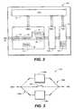
- two or more buffersmay be employed in the EBU 104 , such as shown in FIG. 3 .
- two buffers 104 a and 104 bare used, where one of the two buffers is receiving data from the memory 20 through FIM 18 and the other is sending data to the Crypto-Engine 40 through FDMA 34 in BMU 14 .
- two switches 106 a and 106 bare used. When the two switches are in the solid line positions as shown in FIG. 3 , buffer 104 a is supplying data to the BMU 14 and buffer 104 b is receiving data from FIM 18 . When the two switches are in the dotted line positions as shown in FIG.
- buffer 104 bis supplying data to the BMU 14 and buffer 104 a is receiving data from FIM 18 .
- Each of the bufferscan first be filled with data before data stored in it is sent to the BMU.
- the CPUcorrects the error(s) in the buffer(s) 104 a and 104 b when data is sent from or received by them. In this manner, the only latency is the time required to fill one of the two buffers when the data stream is started. After that, there will be no interruption in the data stream even when error(s) have been detected by circuit 102 , if the time taken by the CPU to correct the error(s) is small compared to the time needed to fill each buffer.
- a buffer-empty signal(not shown) connecting between the EBU 104 and the FDMA 34 signals the latter that the data stream is interrupted and no more data is available.
- the FDMA 34 as well as the crypto engine 40will then pause and wait for the data stream to resume.
- switch 108When data is written by the host device 24 to memory 20 , there may be no need for error correction, so that it would be desirable to bypass the EBU. This may be accomplished by switch 108 .
- switch 108When switch 108 is closed, the data from HIM 16 (not completely shown in FIG. 2 ) simply bypasses the two buffers 104 a and 104 b .
- Switch 108may also be closed in a bypass mode where no cryptographic processing is needed when data is read from or written to memory 20 . In this mode, HDMA and FDMA are connected directly to arbiter 36 as if crypto-engine 40 is eliminated from system 10 , and the data stream bypasses both the EBU 104 and the Crypto-Engine 40 . This may be accomplished also by using switches.
- a logic circuit(not shown) in system 100 under the control of CPU 12 causes the data stream to bypass block 40 and causes switch 108 to close.
- the error correction processis illustrated by the flow chart of FIG. 4 .
- the CPU 12starts a read operation after receiving a read command from the host device 24 (ellipse 150 ). It then configures the Crypto-Engine 40 by writing appropriate security configuration information or record to register 52 , and configures the BMU 14 for a reading operation, and other parameters such as the allocation of memory space in BRAM 38 for the operation (blocks 152 , 154 ). It also configures the FIM 18 , such as by specifying the locations in memory 20 where data is to be read (block 156 ). The HDMA and FDMA engines 32 and 34 are then started. See Block 158 . When the CPU receives an interrupt, it checks to see whether it is a FIM interrupt (diamond 160 ).
- the CPUchecks to see whether the interrupt is one indicating that there is one or more errors in the data stream ( 162 ). If error(s) is indicated, it proceeds to correct the error(s) (block 164 ) in buffers 104 a and/or 104 b and returns to configure the FIM 18 to change the locations in memory 20 where data is to be read next (block 156 ).
- the FIM interruptdoes not indicate error(s) in the data stream, it means the FIM has completed its operation and the CPU also returns to block 156 to re-configure and restart the FIM.
- the interrupt detected by the CPUis not a FIM interrupt, it checks to see if it is an end of data interrupt (diamond 166 ). If it is, then the read operation ends (ellipse 168 ). If not, this interrupt is irrelevant to the cryptographic processing of the data (i.e. clock interrupt) and the CPU 12 services it (not shown) and returns to diamond 160 to check for interrupts.
- FIG. 4needs only to be modified slightly for a write operation. Since there is no handling of ECC errors in the data to be written to memory 20 , the CPU 12 can skip the processes in diamond 162 and block 164 in a write operation. If a FIM interrupt is received by the CPU 12 during a write operation, this means that the FIM completed its operation and the CPU also returns to block 156 to re-configure the FIM. Aside from this difference, the write operation is substantially similar to the read operation.
Landscapes
- Engineering & Computer Science (AREA)
- Computer Security & Cryptography (AREA)
- Computer Networks & Wireless Communication (AREA)
- Signal Processing (AREA)
- Techniques For Improving Reliability Of Storages (AREA)
Abstract
Description
Claims (12)
Priority Applications (7)
| Application Number | Priority Date | Filing Date | Title |
|---|---|---|---|
| US11/313,428US8396208B2 (en) | 2004-12-21 | 2005-12-20 | Memory system with in stream data encryption/decryption and error correction |
| CN2005800484386ACN101124545B (en) | 2004-12-21 | 2005-12-21 | Memory system with in-stream data encryption/decryption and error correction |
| JP2007548490AJP2008524754A (en) | 2004-12-21 | 2005-12-21 | Memory system having in-stream data encryption / decryption and error correction functions |
| EP05855273AEP1828898A2 (en) | 2004-12-21 | 2005-12-21 | Memory system with in stream data encryption/decryption and error correction |
| TW094145661ATWI391945B (en) | 2004-12-21 | 2005-12-21 | Memory system with in stream data encryption/decryption and error correction and method for correcting data in the memory system |
| PCT/US2005/046688WO2006069273A2 (en) | 2004-12-21 | 2005-12-21 | Memory system with in stream data encryption/decryption and error correction |
| KR1020077016699AKR101254136B1 (en) | 2004-12-21 | 2005-12-21 | Memory System with In Stream Data Encryption/Decryption and Error Correction |
Applications Claiming Priority (2)
| Application Number | Priority Date | Filing Date | Title |
|---|---|---|---|
| US63848504P | 2004-12-21 | 2004-12-21 | |
| US11/313,428US8396208B2 (en) | 2004-12-21 | 2005-12-20 | Memory system with in stream data encryption/decryption and error correction |
Publications (2)
| Publication Number | Publication Date |
|---|---|
| US20060239449A1 US20060239449A1 (en) | 2006-10-26 |
| US8396208B2true US8396208B2 (en) | 2013-03-12 |
Family
ID=37186904
Family Applications (1)
| Application Number | Title | Priority Date | Filing Date |
|---|---|---|---|
| US11/313,428Active2028-06-28US8396208B2 (en) | 2004-12-21 | 2005-12-20 | Memory system with in stream data encryption/decryption and error correction |
Country Status (1)
| Country | Link |
|---|---|
| US (1) | US8396208B2 (en) |
Cited By (2)
| Publication number | Priority date | Publication date | Assignee | Title |
|---|---|---|---|---|
| US20120321088A1 (en)* | 2009-11-09 | 2012-12-20 | Siemens Aktiengesellschaft | Method And System For The Accelerated Decryption Of Cryptographically Protected User Data Units |
| US20190165929A1 (en)* | 2016-07-29 | 2019-05-30 | Permanent Privacy Ltd | Applications in connection with secure encryption |
Families Citing this family (7)
| Publication number | Priority date | Publication date | Assignee | Title |
|---|---|---|---|---|
| US8108691B2 (en) | 2005-02-07 | 2012-01-31 | Sandisk Technologies Inc. | Methods used in a secure memory card with life cycle phases |
| US8423788B2 (en) | 2005-02-07 | 2013-04-16 | Sandisk Technologies Inc. | Secure memory card with life cycle phases |
| US8321686B2 (en)* | 2005-02-07 | 2012-11-27 | Sandisk Technologies Inc. | Secure memory card with life cycle phases |
| US7748031B2 (en) | 2005-07-08 | 2010-06-29 | Sandisk Corporation | Mass storage device with automated credentials loading |
| WO2011064883A1 (en)* | 2009-11-27 | 2011-06-03 | 株式会社東芝 | Memory chip |
| KR101052600B1 (en) | 2010-02-22 | 2011-07-29 | 주식회사 셀픽 | Encrypted data storage device and its storage method |
| US20120237024A1 (en)* | 2011-03-18 | 2012-09-20 | Wei-Ti Liu | Security System Using Physical Key for Cryptographic Processes |
Citations (43)
| Publication number | Priority date | Publication date | Assignee | Title |
|---|---|---|---|---|
| US4375664A (en)* | 1980-06-03 | 1983-03-01 | Burroughs Corporation | Apparatus for detecting, correcting and logging single bit memory read errors using syndrome generating and decoding circuitry |
| US4506362A (en)* | 1978-12-22 | 1985-03-19 | Gould Inc. | Systematic memory error detection and correction apparatus and method |
| US4506365A (en)* | 1982-11-22 | 1985-03-19 | Ncr Corporation | Error correction system |
| JPS642136A (en) | 1987-06-25 | 1989-01-06 | Fujitsu Ltd | System for controlling fifo buffer |
| US5438575A (en)* | 1992-11-16 | 1995-08-01 | Ampex Corporation | Data storage system with stale data detector and method of operation |
| WO1998026535A1 (en) | 1996-12-12 | 1998-06-18 | Intel Corporation | Cryptographically protected paging subsystem |
| JPH113284A (en) | 1997-06-10 | 1999-01-06 | Mitsubishi Electric Corp | Information storage medium and security method thereof |
| EP1074906A1 (en) | 1999-08-05 | 2001-02-07 | Sony Corporation | Card-shaped semiconductor storage device and operation setting method of the same |
| US20010016875A1 (en)* | 1997-07-11 | 2001-08-23 | Schwartz Bruce V. | Reducing perceived latency in servicing user requests on low-bandwidth communication channels |
| US20010018741A1 (en) | 1997-07-17 | 2001-08-30 | Hogan Josh N. | Method and apparatus for performing data encryption and error code correction |
| JP2002229861A (en) | 2001-02-07 | 2002-08-16 | Hitachi Ltd | Recording device with copyright protection function |
| JP2002329180A (en) | 2001-04-27 | 2002-11-15 | Toshiba Corp | Memory card having wireless communication function and data communication method thereof |
| US20020188812A1 (en)* | 2001-06-12 | 2002-12-12 | Akila Sadhasivan | Implementing a dual partition flash with suspend/resume capabilities |
| US20030018664A1 (en)* | 2001-05-04 | 2003-01-23 | Wee Susie J. | Method and system for midstream transcoding of scalable packets in response to downstream requirements |
| US20030016875A1 (en)* | 2001-07-10 | 2003-01-23 | Nec Corporation | Image encoder, image encoding method, recording medium and computer data signal embodied in a carrier wave |
| US20030085289A1 (en)* | 2001-11-08 | 2003-05-08 | Yoshio Kaneko | Memory card and contents distributing system and method |
| US20030097344A1 (en) | 1994-01-11 | 2003-05-22 | David Chaum | Multi-purpose transaction card system |
| US20030097655A1 (en)* | 2001-11-21 | 2003-05-22 | Novak Robert E. | System and method for providing conditional access to digital content |
| US20030196028A1 (en)* | 1999-10-21 | 2003-10-16 | Takuji Maeda | Semiconductor memory card access apparatus, a computer-readable recording medium, an initialization method, and a semiconductor memory card |
| US20030233545A1 (en) | 2002-06-13 | 2003-12-18 | Avigdor Eldar | Diagnostic method for security records in networking application |
| JP2004110253A (en) | 2002-09-17 | 2004-04-08 | Ricoh Co Ltd | File management device |
| US20040105549A1 (en)* | 2002-11-15 | 2004-06-03 | Nec Corporation | Key mangement system and multicast delivery system using the same |
| US6754765B1 (en) | 2001-05-14 | 2004-06-22 | Integrated Memory Logic, Inc. | Flash memory controller with updateable microcode |
| US20040139380A1 (en) | 2001-04-27 | 2004-07-15 | Yoichiro Sako | Method of recording on recording medium and recording device, and method of reproducing from recording meidumand reproducing device |
| US20040153918A1 (en) | 2002-04-08 | 2004-08-05 | Matsushita Electric Industrial Co., | Tamper-resistant computer program product |
| US20040172538A1 (en) | 2002-12-18 | 2004-09-02 | International Business Machines Corporation | Information processing with data storage |
| US20040223618A1 (en)* | 2003-02-04 | 2004-11-11 | Stmicroelectronics Limited | Decryption semiconductor circuit |
| US20040250092A1 (en)* | 2003-03-28 | 2004-12-09 | Yoshihiro Hori | Method and apparatus for encrypting data to be secured and inputting/outputting the same |
| US20050060602A1 (en)* | 2003-08-06 | 2005-03-17 | Stmicroelectronics S.R.L. | Memory system with error detection device |
| US20050063265A1 (en) | 2003-09-11 | 2005-03-24 | Jun Akiyama | Data storage medium reproducing device and method for reproducing data storage medium |
| US6928599B2 (en)* | 2001-12-05 | 2005-08-09 | Intel Corporation | Method and apparatus for decoding data |
| US20050273618A1 (en) | 2002-09-11 | 2005-12-08 | Itaru Takemura | Information recording medium, information recording device, information reproduction device, information delivery device, their methods, their programs, and recording medium recording programs thereon |
| US20060031722A1 (en) | 2004-08-04 | 2006-02-09 | International Business Machines Corporation | Apparatus, system, and method for active data verification in a storage system |
| US20060036897A1 (en)* | 2004-08-13 | 2006-02-16 | Chanson Lin | Data storage device |
| US7036020B2 (en) | 2001-07-25 | 2006-04-25 | Antique Books, Inc | Methods and systems for promoting security in a computer system employing attached storage devices |
| US20060107047A1 (en)* | 2004-11-12 | 2006-05-18 | Hagai Bar-El | Method, device, and system of securely storing data |
| US20060232826A1 (en)* | 2005-04-13 | 2006-10-19 | Hagai Bar-El | Method, device, and system of selectively accessing data |
| US20060262928A1 (en)* | 2005-05-23 | 2006-11-23 | Hagai Bar-El | Method, device, and system of encrypting/decrypting data |
| US20060294513A1 (en) | 2005-06-22 | 2006-12-28 | Hagai Bar-El | System, device, and method of selectively allowing a host processor to access host-executable code |
| US20060294236A1 (en) | 2005-06-22 | 2006-12-28 | Hagai Bar-El | System, device, and method of selectively operating a host connected to a token |
| US7180843B2 (en)* | 2002-06-07 | 2007-02-20 | Fujitsu Limited | Information recording and reproduction apparatus, optical disk apparatus and data reproduction method |
| US7215771B1 (en) | 2000-06-30 | 2007-05-08 | Western Digital Ventures, Inc. | Secure disk drive comprising a secure drive key and a drive ID for implementing secure communication over a public network |
| US7493656B2 (en) | 2005-06-02 | 2009-02-17 | Seagate Technology Llc | Drive security session manager |
Family Cites Families (1)
| Publication number | Priority date | Publication date | Assignee | Title |
|---|---|---|---|---|
| US8398668B2 (en)* | 2006-04-19 | 2013-03-19 | Vibrynt, Inc. | Devices and methods for treatment of obesity |
- 2005
- 2005-12-20USUS11/313,428patent/US8396208B2/enactiveActive
Patent Citations (53)
| Publication number | Priority date | Publication date | Assignee | Title |
|---|---|---|---|---|
| US4506362A (en)* | 1978-12-22 | 1985-03-19 | Gould Inc. | Systematic memory error detection and correction apparatus and method |
| US4375664A (en)* | 1980-06-03 | 1983-03-01 | Burroughs Corporation | Apparatus for detecting, correcting and logging single bit memory read errors using syndrome generating and decoding circuitry |
| US4506365A (en)* | 1982-11-22 | 1985-03-19 | Ncr Corporation | Error correction system |
| JPS642136A (en) | 1987-06-25 | 1989-01-06 | Fujitsu Ltd | System for controlling fifo buffer |
| US5438575A (en)* | 1992-11-16 | 1995-08-01 | Ampex Corporation | Data storage system with stale data detector and method of operation |
| US20030097344A1 (en) | 1994-01-11 | 2003-05-22 | David Chaum | Multi-purpose transaction card system |
| WO1998026535A1 (en) | 1996-12-12 | 1998-06-18 | Intel Corporation | Cryptographically protected paging subsystem |
| JP2001508893A (en) | 1996-12-12 | 2001-07-03 | インテル・コーポレーション | Paging system protected by cryptography |
| JPH113284A (en) | 1997-06-10 | 1999-01-06 | Mitsubishi Electric Corp | Information storage medium and security method thereof |
| US6158004A (en)* | 1997-06-10 | 2000-12-05 | Mitsubishi Denki Kabushiki Kaisha | Information storage medium and security method thereof |
| US20010016875A1 (en)* | 1997-07-11 | 2001-08-23 | Schwartz Bruce V. | Reducing perceived latency in servicing user requests on low-bandwidth communication channels |
| US20010018741A1 (en) | 1997-07-17 | 2001-08-30 | Hogan Josh N. | Method and apparatus for performing data encryption and error code correction |
| US6513719B1 (en) | 1999-08-05 | 2003-02-04 | Sony Corporation | Card-shaped semiconductor storage device and operation setting method of the same |
| JP2001051903A (en) | 1999-08-05 | 2001-02-23 | Sony Corp | Semiconductor storage device and operation setting method for semiconductor storage device |
| EP1074906A1 (en) | 1999-08-05 | 2001-02-07 | Sony Corporation | Card-shaped semiconductor storage device and operation setting method of the same |
| US6829676B2 (en)* | 1999-10-21 | 2004-12-07 | Matsushita Electric Industrial Co., Ltd. | Semiconductor memory card access apparatus, a computer-readable recording medium, an initialization method, and a semiconductor memory card |
| US20030196028A1 (en)* | 1999-10-21 | 2003-10-16 | Takuji Maeda | Semiconductor memory card access apparatus, a computer-readable recording medium, an initialization method, and a semiconductor memory card |
| US7215771B1 (en) | 2000-06-30 | 2007-05-08 | Western Digital Ventures, Inc. | Secure disk drive comprising a secure drive key and a drive ID for implementing secure communication over a public network |
| JP2002229861A (en) | 2001-02-07 | 2002-08-16 | Hitachi Ltd | Recording device with copyright protection function |
| US20020169960A1 (en) | 2001-02-07 | 2002-11-14 | Shinya Iguchi | Storage device including a non-volatile memory |
| US20020174337A1 (en)* | 2001-04-27 | 2002-11-21 | Tadahiro Aihara | Memory card with wireless communication function and data communication method |
| JP2002329180A (en) | 2001-04-27 | 2002-11-15 | Toshiba Corp | Memory card having wireless communication function and data communication method thereof |
| US20040139380A1 (en) | 2001-04-27 | 2004-07-15 | Yoichiro Sako | Method of recording on recording medium and recording device, and method of reproducing from recording meidumand reproducing device |
| US20030018664A1 (en)* | 2001-05-04 | 2003-01-23 | Wee Susie J. | Method and system for midstream transcoding of scalable packets in response to downstream requirements |
| US6754765B1 (en) | 2001-05-14 | 2004-06-22 | Integrated Memory Logic, Inc. | Flash memory controller with updateable microcode |
| US20020188812A1 (en)* | 2001-06-12 | 2002-12-12 | Akila Sadhasivan | Implementing a dual partition flash with suspend/resume capabilities |
| US7062616B2 (en)* | 2001-06-12 | 2006-06-13 | Intel Corporation | Implementing a dual partition flash with suspend/resume capabilities |
| US20030016875A1 (en)* | 2001-07-10 | 2003-01-23 | Nec Corporation | Image encoder, image encoding method, recording medium and computer data signal embodied in a carrier wave |
| US7426747B2 (en) | 2001-07-25 | 2008-09-16 | Antique Books, Inc. | Methods and systems for promoting security in a computer system employing attached storage devices |
| US7036020B2 (en) | 2001-07-25 | 2006-04-25 | Antique Books, Inc | Methods and systems for promoting security in a computer system employing attached storage devices |
| US6832731B2 (en)* | 2001-11-08 | 2004-12-21 | Kabushiki Kaisha Toshiba | Memory card and contents distributing system and method |
| US20030085289A1 (en)* | 2001-11-08 | 2003-05-08 | Yoshio Kaneko | Memory card and contents distributing system and method |
| US20030097655A1 (en)* | 2001-11-21 | 2003-05-22 | Novak Robert E. | System and method for providing conditional access to digital content |
| US6928599B2 (en)* | 2001-12-05 | 2005-08-09 | Intel Corporation | Method and apparatus for decoding data |
| US20040153918A1 (en) | 2002-04-08 | 2004-08-05 | Matsushita Electric Industrial Co., | Tamper-resistant computer program product |
| US7180843B2 (en)* | 2002-06-07 | 2007-02-20 | Fujitsu Limited | Information recording and reproduction apparatus, optical disk apparatus and data reproduction method |
| US20030233545A1 (en) | 2002-06-13 | 2003-12-18 | Avigdor Eldar | Diagnostic method for security records in networking application |
| US20050273618A1 (en) | 2002-09-11 | 2005-12-08 | Itaru Takemura | Information recording medium, information recording device, information reproduction device, information delivery device, their methods, their programs, and recording medium recording programs thereon |
| JP2004110253A (en) | 2002-09-17 | 2004-04-08 | Ricoh Co Ltd | File management device |
| US20040105549A1 (en)* | 2002-11-15 | 2004-06-03 | Nec Corporation | Key mangement system and multicast delivery system using the same |
| US20040172538A1 (en) | 2002-12-18 | 2004-09-02 | International Business Machines Corporation | Information processing with data storage |
| US20040223618A1 (en)* | 2003-02-04 | 2004-11-11 | Stmicroelectronics Limited | Decryption semiconductor circuit |
| US20040250092A1 (en)* | 2003-03-28 | 2004-12-09 | Yoshihiro Hori | Method and apparatus for encrypting data to be secured and inputting/outputting the same |
| US20050060602A1 (en)* | 2003-08-06 | 2005-03-17 | Stmicroelectronics S.R.L. | Memory system with error detection device |
| US20050063265A1 (en) | 2003-09-11 | 2005-03-24 | Jun Akiyama | Data storage medium reproducing device and method for reproducing data storage medium |
| US20060031722A1 (en) | 2004-08-04 | 2006-02-09 | International Business Machines Corporation | Apparatus, system, and method for active data verification in a storage system |
| US20060036897A1 (en)* | 2004-08-13 | 2006-02-16 | Chanson Lin | Data storage device |
| US20060107047A1 (en)* | 2004-11-12 | 2006-05-18 | Hagai Bar-El | Method, device, and system of securely storing data |
| US20060232826A1 (en)* | 2005-04-13 | 2006-10-19 | Hagai Bar-El | Method, device, and system of selectively accessing data |
| US20060262928A1 (en)* | 2005-05-23 | 2006-11-23 | Hagai Bar-El | Method, device, and system of encrypting/decrypting data |
| US7493656B2 (en) | 2005-06-02 | 2009-02-17 | Seagate Technology Llc | Drive security session manager |
| US20060294513A1 (en) | 2005-06-22 | 2006-12-28 | Hagai Bar-El | System, device, and method of selectively allowing a host processor to access host-executable code |
| US20060294236A1 (en) | 2005-06-22 | 2006-12-28 | Hagai Bar-El | System, device, and method of selectively operating a host connected to a token |
Non-Patent Citations (19)
| Title |
|---|
| Invitation to Pay Additional Fees and a Partial International Search Report for PCT/US2005/046586, dated Jul. 11, 2006, 8 pages. |
| Notification of Transmittal of the International Search Report and the Written Opinion of the International Searching Authority, or the Declaration for PCT/US2005/046586, dated Oct. 12, 2006, 5 pages. |
| Notification of Transmittal of the International Search Report and the Written Opinion of the International Searching Authority, or the Declaration, in corresponding PCT/US2005/046688, dated Sep. 19, 2006, 14 pages. |
| Office Action for Chinese Patent Application Serial No. 200580048239.5, dated Sep. 27, 2012, 5 pages. |
| Office Action for Japanese Patent Application Serial No. 2007-548469, dated May 17, 2011, 22 pages. |
| Office Action for Japanese Patent Application Serial No. 2007-548490, dated Feb. 7, 2012, 5 pages. |
| Office Action for Japanese Patent Application Serial No. 2007-548490, dated Jun. 14, 2011, 7 pages. |
| Office Action for Japanese Patent Application Serial No. 2007-548490, dated Sep. 4, 2012, 2 pages. |
| Office Action for Japanese Patent Application Serial No. JP 2007-548469, dated Mar. 21, 2012, 9 pages. |
| Office Action for Korean Patent Application Serial No. KR 10-2007-7016699, dated Jun. 20, 2012, 6 pages. |
| Office Action for Korean Patent Application Serial No. KR 10-2007-7016700, dated Jun. 19, 2010, 5 pages. |
| Office Action for Taiwanese Patent Application Serial No. 094145661, dated Sep. 12, 2012, 15 pages. |
| Office Action for Taiwanese Patent Application Serial No. 094145713, dated Mar. 26, 2012, 20 pages. |
| Office Action for U.S. Appl. No. 11/313,447, 13 pages, Apr. 14, 2009. |
| Office Action for U.S. Appl. No. 11/314,030, dated Dec. 9, 2010, 20 pages. |
| Office Action for U.S. Appl. No. 11/314,030, dated Mar. 30, 2010, 14 pages. |
| Office Action for U.S. Appl. No. 11/314,032, dated Mar. 30, 2010, 15 pages. |
| Search Report for European Patent Application Serial No. 10177325.7, dated Dec. 27, 2010, 4 pages. |
| Search Report for European Patent Application Serial No. EP10182649, dated Apr. 1, 2011, 5 pages. |
Cited By (4)
| Publication number | Priority date | Publication date | Assignee | Title |
|---|---|---|---|---|
| US20120321088A1 (en)* | 2009-11-09 | 2012-12-20 | Siemens Aktiengesellschaft | Method And System For The Accelerated Decryption Of Cryptographically Protected User Data Units |
| US9571273B2 (en)* | 2009-11-09 | 2017-02-14 | Siemens Aktiengesellschaft | Method and system for the accelerated decryption of cryptographically protected user data units |
| US20190165929A1 (en)* | 2016-07-29 | 2019-05-30 | Permanent Privacy Ltd | Applications in connection with secure encryption |
| US11784793B2 (en)* | 2016-07-29 | 2023-10-10 | Permanent Privacy Ltd. | Applications in connection with secure encryption |
Also Published As
| Publication number | Publication date |
|---|---|
| US20060239449A1 (en) | 2006-10-26 |
Similar Documents
| Publication | Publication Date | Title |
|---|---|---|
| US6769087B2 (en) | Data storage device and method for controlling the device | |
| US20060239450A1 (en) | In stream data encryption / decryption and error correction method | |
| US20060242429A1 (en) | In stream data encryption / decryption method | |
| US8291295B2 (en) | NAND flash memory controller exporting a NAND interface | |
| US20140250348A1 (en) | Controller and Method for Interfacing Between a Host Controller in a Host and a Flash Memory Device | |
| US20110040924A1 (en) | Controller and Method for Detecting a Transmission Error Over a NAND Interface Using Error Detection Code | |
| US20230004649A1 (en) | Memory device having safety boot capability | |
| US20110041005A1 (en) | Controller and Method for Providing Read Status and Spare Block Management Information in a Flash Memory System | |
| US7835518B2 (en) | System and method for write failure recovery | |
| US8396208B2 (en) | Memory system with in stream data encryption/decryption and error correction | |
| KR101254136B1 (en) | Memory System with In Stream Data Encryption/Decryption and Error Correction | |
| US20070230690A1 (en) | System for write failure recovery | |
| EP1828948B1 (en) | Memory system with in-stream data encryption/decryption | |
| US12086457B2 (en) | Managing secure writes in semiconductor devices | |
| US7966539B2 (en) | Digital content protection systems and methods | |
| WO2007118034A2 (en) | System and method for write failure recovery |
Legal Events
| Date | Code | Title | Description |
|---|---|---|---|
| AS | Assignment | Owner name:SANDISK CORPORATION, CALIFORNIA Free format text:ASSIGNMENT OF ASSIGNORS INTEREST;ASSIGNORS:HOLTZMAN, MICHAEL;COHEN, BARUCH BORIS;RIJWANE UL ISLAM, MUHAMMED;AND OTHERS;SIGNING DATES FROM 20060613 TO 20060621;REEL/FRAME:018244/0872 Owner name:SANDISK CORPORATION, CALIFORNIA Free format text:ASSIGNMENT OF ASSIGNORS INTEREST;ASSIGNORS:HOLTZMAN, MICHAEL;COHEN, BARUCH BORIS;RIJWANE UL ISLAM, MUHAMMED;AND OTHERS;REEL/FRAME:018244/0872;SIGNING DATES FROM 20060613 TO 20060621 | |
| AS | Assignment | Owner name:SANDISK TECHNOLOGIES INC., TEXAS Free format text:ASSIGNMENT OF ASSIGNORS INTEREST;ASSIGNOR:SANDISK CORPORATION;REEL/FRAME:026346/0224 Effective date:20110404 | |
| STCF | Information on status: patent grant | Free format text:PATENTED CASE | |
| AS | Assignment | Owner name:SANDISK TECHNOLOGIES LLC, TEXAS Free format text:CHANGE OF NAME;ASSIGNOR:SANDISK TECHNOLOGIES INC;REEL/FRAME:038809/0472 Effective date:20160516 | |
| FPAY | Fee payment | Year of fee payment:4 | |
| MAFP | Maintenance fee payment | Free format text:PAYMENT OF MAINTENANCE FEE, 8TH YEAR, LARGE ENTITY (ORIGINAL EVENT CODE: M1552); ENTITY STATUS OF PATENT OWNER: LARGE ENTITY Year of fee payment:8 | |
| MAFP | Maintenance fee payment | Free format text:PAYMENT OF MAINTENANCE FEE, 12TH YEAR, LARGE ENTITY (ORIGINAL EVENT CODE: M1553); ENTITY STATUS OF PATENT OWNER: LARGE ENTITY Year of fee payment:12 | |
| AS | Assignment | Owner name:SANDISK TECHNOLOGIES, INC., CALIFORNIA Free format text:ASSIGNMENT OF ASSIGNORS INTEREST;ASSIGNOR:SANDISK TECHNOLOGIES LLC;REEL/FRAME:069796/0423 Effective date:20241227 | |
| AS | Assignment | Owner name:SANDISK TECHNOLOGIES, INC., CALIFORNIA Free format text:PARTIAL RELEASE OF SECURITY INTERESTS;ASSIGNOR:JPMORGAN CHASE BANK, N.A., AS AGENT;REEL/FRAME:071382/0001 Effective date:20250424 Owner name:JPMORGAN CHASE BANK, N.A., AS COLLATERAL AGENT, ILLINOIS Free format text:SECURITY AGREEMENT;ASSIGNOR:SANDISK TECHNOLOGIES, INC.;REEL/FRAME:071050/0001 Effective date:20250424 |