US8395942B2 - Junctionless TFT NAND flash memory - Google Patents
Junctionless TFT NAND flash memoryDownload PDFInfo
- Publication number
- US8395942B2 US8395942B2US12/848,458US84845810AUS8395942B2US 8395942 B2US8395942 B2US 8395942B2US 84845810 AUS84845810 AUS 84845810AUS 8395942 B2US8395942 B2US 8395942B2
- Authority
- US
- United States
- Prior art keywords
- channel
- charge storage
- erase
- memory
- dielectric layer
- Prior art date
- Legal status (The legal status is an assumption and is not a legal conclusion. Google has not performed a legal analysis and makes no representation as to the accuracy of the status listed.)
- Expired - Fee Related, expires
Links
Images


Classifications
- H—ELECTRICITY
- H10—SEMICONDUCTOR DEVICES; ELECTRIC SOLID-STATE DEVICES NOT OTHERWISE PROVIDED FOR
- H10D—INORGANIC ELECTRIC SEMICONDUCTOR DEVICES
- H10D30/00—Field-effect transistors [FET]
- H10D30/01—Manufacture or treatment
- H10D30/021—Manufacture or treatment of FETs having insulated gates [IGFET]
- H10D30/0411—Manufacture or treatment of FETs having insulated gates [IGFET] of FETs having floating gates
- H—ELECTRICITY
- H10—SEMICONDUCTOR DEVICES; ELECTRIC SOLID-STATE DEVICES NOT OTHERWISE PROVIDED FOR
- H10D—INORGANIC ELECTRIC SEMICONDUCTOR DEVICES
- H10D86/00—Integrated devices formed in or on insulating or conducting substrates, e.g. formed in silicon-on-insulator [SOI] substrates or on stainless steel or glass substrates
- H10D86/40—Integrated devices formed in or on insulating or conducting substrates, e.g. formed in silicon-on-insulator [SOI] substrates or on stainless steel or glass substrates characterised by multiple TFTs
- B—PERFORMING OPERATIONS; TRANSPORTING
- B82—NANOTECHNOLOGY
- B82Y—SPECIFIC USES OR APPLICATIONS OF NANOSTRUCTURES; MEASUREMENT OR ANALYSIS OF NANOSTRUCTURES; MANUFACTURE OR TREATMENT OF NANOSTRUCTURES
- B82Y10/00—Nanotechnology for information processing, storage or transmission, e.g. quantum computing or single electron logic
- G—PHYSICS
- G11—INFORMATION STORAGE
- G11C—STATIC STORES
- G11C16/00—Erasable programmable read-only memories
- G11C16/02—Erasable programmable read-only memories electrically programmable
- G11C16/04—Erasable programmable read-only memories electrically programmable using variable threshold transistors, e.g. FAMOS
- G11C16/0483—Erasable programmable read-only memories electrically programmable using variable threshold transistors, e.g. FAMOS comprising cells having several storage transistors connected in series
- H—ELECTRICITY
- H10—SEMICONDUCTOR DEVICES; ELECTRIC SOLID-STATE DEVICES NOT OTHERWISE PROVIDED FOR
- H10B—ELECTRONIC MEMORY DEVICES
- H10B20/00—Read-only memory [ROM] devices
- H—ELECTRICITY
- H10—SEMICONDUCTOR DEVICES; ELECTRIC SOLID-STATE DEVICES NOT OTHERWISE PROVIDED FOR
- H10B—ELECTRONIC MEMORY DEVICES
- H10B20/00—Read-only memory [ROM] devices
- H10B20/20—Programmable ROM [PROM] devices comprising field-effect components
- H—ELECTRICITY
- H10—SEMICONDUCTOR DEVICES; ELECTRIC SOLID-STATE DEVICES NOT OTHERWISE PROVIDED FOR
- H10B—ELECTRONIC MEMORY DEVICES
- H10B20/00—Read-only memory [ROM] devices
- H10B20/20—Programmable ROM [PROM] devices comprising field-effect components
- H10B20/25—One-time programmable ROM [OTPROM] devices, e.g. using electrically-fusible links
- H—ELECTRICITY
- H10—SEMICONDUCTOR DEVICES; ELECTRIC SOLID-STATE DEVICES NOT OTHERWISE PROVIDED FOR
- H10B—ELECTRONIC MEMORY DEVICES
- H10B41/00—Electrically erasable-and-programmable ROM [EEPROM] devices comprising floating gates
- H10B41/20—Electrically erasable-and-programmable ROM [EEPROM] devices comprising floating gates characterised by three-dimensional arrangements, e.g. with cells on different height levels
- H10B41/23—Electrically erasable-and-programmable ROM [EEPROM] devices comprising floating gates characterised by three-dimensional arrangements, e.g. with cells on different height levels with source and drain on different levels, e.g. with sloping channels
- H10B41/27—Electrically erasable-and-programmable ROM [EEPROM] devices comprising floating gates characterised by three-dimensional arrangements, e.g. with cells on different height levels with source and drain on different levels, e.g. with sloping channels the channels comprising vertical portions, e.g. U-shaped channels
- H—ELECTRICITY
- H10—SEMICONDUCTOR DEVICES; ELECTRIC SOLID-STATE DEVICES NOT OTHERWISE PROVIDED FOR
- H10B—ELECTRONIC MEMORY DEVICES
- H10B41/00—Electrically erasable-and-programmable ROM [EEPROM] devices comprising floating gates
- H10B41/30—Electrically erasable-and-programmable ROM [EEPROM] devices comprising floating gates characterised by the memory core region
- H10B41/35—Electrically erasable-and-programmable ROM [EEPROM] devices comprising floating gates characterised by the memory core region with a cell select transistor, e.g. NAND
- H—ELECTRICITY
- H10—SEMICONDUCTOR DEVICES; ELECTRIC SOLID-STATE DEVICES NOT OTHERWISE PROVIDED FOR
- H10B—ELECTRONIC MEMORY DEVICES
- H10B43/00—EEPROM devices comprising charge-trapping gate insulators
- H10B43/20—EEPROM devices comprising charge-trapping gate insulators characterised by three-dimensional arrangements, e.g. with cells on different height levels
- H—ELECTRICITY
- H10—SEMICONDUCTOR DEVICES; ELECTRIC SOLID-STATE DEVICES NOT OTHERWISE PROVIDED FOR
- H10B—ELECTRONIC MEMORY DEVICES
- H10B63/00—Resistance change memory devices, e.g. resistive RAM [ReRAM] devices
- H10B63/10—Phase change RAM [PCRAM, PRAM] devices
- H—ELECTRICITY
- H10—SEMICONDUCTOR DEVICES; ELECTRIC SOLID-STATE DEVICES NOT OTHERWISE PROVIDED FOR
- H10D—INORGANIC ELECTRIC SEMICONDUCTOR DEVICES
- H10D30/00—Field-effect transistors [FET]
- H10D30/01—Manufacture or treatment
- H10D30/021—Manufacture or treatment of FETs having insulated gates [IGFET]
- H10D30/0413—Manufacture or treatment of FETs having insulated gates [IGFET] of FETs having charge-trapping gate insulators, e.g. MNOS transistors
- H—ELECTRICITY
- H10—SEMICONDUCTOR DEVICES; ELECTRIC SOLID-STATE DEVICES NOT OTHERWISE PROVIDED FOR
- H10D—INORGANIC ELECTRIC SEMICONDUCTOR DEVICES
- H10D30/00—Field-effect transistors [FET]
- H10D30/60—Insulated-gate field-effect transistors [IGFET]
- H10D30/68—Floating-gate IGFETs
- H10D30/681—Floating-gate IGFETs having only two programming levels
- H—ELECTRICITY
- H10—SEMICONDUCTOR DEVICES; ELECTRIC SOLID-STATE DEVICES NOT OTHERWISE PROVIDED FOR
- H10D—INORGANIC ELECTRIC SEMICONDUCTOR DEVICES
- H10D30/00—Field-effect transistors [FET]
- H10D30/60—Insulated-gate field-effect transistors [IGFET]
- H10D30/69—IGFETs having charge trapping gate insulators, e.g. MNOS transistors
- H—ELECTRICITY
- H10—SEMICONDUCTOR DEVICES; ELECTRIC SOLID-STATE DEVICES NOT OTHERWISE PROVIDED FOR
- H10D—INORGANIC ELECTRIC SEMICONDUCTOR DEVICES
- H10D84/00—Integrated devices formed in or on semiconductor substrates that comprise only semiconducting layers, e.g. on Si wafers or on GaAs-on-Si wafers
- H10D84/01—Manufacture or treatment
- H10D84/02—Manufacture or treatment characterised by using material-based technologies
- H10D84/03—Manufacture or treatment characterised by using material-based technologies using Group IV technology, e.g. silicon technology or silicon-carbide [SiC] technology
- H10D84/038—Manufacture or treatment characterised by using material-based technologies using Group IV technology, e.g. silicon technology or silicon-carbide [SiC] technology using silicon technology, e.g. SiGe
- H—ELECTRICITY
- H10—SEMICONDUCTOR DEVICES; ELECTRIC SOLID-STATE DEVICES NOT OTHERWISE PROVIDED FOR
- H10D—INORGANIC ELECTRIC SEMICONDUCTOR DEVICES
- H10D86/00—Integrated devices formed in or on insulating or conducting substrates, e.g. formed in silicon-on-insulator [SOI] substrates or on stainless steel or glass substrates
- H10D86/01—Manufacture or treatment
- H—ELECTRICITY
- H10—SEMICONDUCTOR DEVICES; ELECTRIC SOLID-STATE DEVICES NOT OTHERWISE PROVIDED FOR
- H10D—INORGANIC ELECTRIC SEMICONDUCTOR DEVICES
- H10D86/00—Integrated devices formed in or on insulating or conducting substrates, e.g. formed in silicon-on-insulator [SOI] substrates or on stainless steel or glass substrates
- H10D86/201—Integrated devices formed in or on insulating or conducting substrates, e.g. formed in silicon-on-insulator [SOI] substrates or on stainless steel or glass substrates the substrates comprising an insulating layer on a semiconductor body, e.g. SOI
- H—ELECTRICITY
- H10—SEMICONDUCTOR DEVICES; ELECTRIC SOLID-STATE DEVICES NOT OTHERWISE PROVIDED FOR
- H10D—INORGANIC ELECTRIC SEMICONDUCTOR DEVICES
- H10D86/00—Integrated devices formed in or on insulating or conducting substrates, e.g. formed in silicon-on-insulator [SOI] substrates or on stainless steel or glass substrates
- H10D86/40—Integrated devices formed in or on insulating or conducting substrates, e.g. formed in silicon-on-insulator [SOI] substrates or on stainless steel or glass substrates characterised by multiple TFTs
- H10D86/60—Integrated devices formed in or on insulating or conducting substrates, e.g. formed in silicon-on-insulator [SOI] substrates or on stainless steel or glass substrates characterised by multiple TFTs wherein the TFTs are in active matrices
- H—ELECTRICITY
- H10—SEMICONDUCTOR DEVICES; ELECTRIC SOLID-STATE DEVICES NOT OTHERWISE PROVIDED FOR
- H10D—INORGANIC ELECTRIC SEMICONDUCTOR DEVICES
- H10D88/00—Three-dimensional [3D] integrated devices
- H—ELECTRICITY
- H10—SEMICONDUCTOR DEVICES; ELECTRIC SOLID-STATE DEVICES NOT OTHERWISE PROVIDED FOR
- H10D—INORGANIC ELECTRIC SEMICONDUCTOR DEVICES
- H10D88/00—Three-dimensional [3D] integrated devices
- H10D88/01—Manufacture or treatment
- H—ELECTRICITY
- H10—SEMICONDUCTOR DEVICES; ELECTRIC SOLID-STATE DEVICES NOT OTHERWISE PROVIDED FOR
- H10B—ELECTRONIC MEMORY DEVICES
- H10B43/00—EEPROM devices comprising charge-trapping gate insulators
- H10B43/30—EEPROM devices comprising charge-trapping gate insulators characterised by the memory core region
Definitions
- the present inventionis directed to semiconductor devices, particularly memory devices, and methods of fabricating and using same.
- RAMrandom-access memory
- ROMread only memory
- SDRAMsynchronous dynamic random access memory
- DRAMdynamic random access memory
- flash memoryas described, for example, in U.S. Pat. No. 5,677,556 and US published application 2006/0278913 A1, both of which are incorporated herein by reference in their entirety.
- Flash memoryis a type of non-volatile memory that can be rewritten electronically for multiple times.
- Typical flash memory devicesare based on MOSFET technologies having architectures similar to those of NOR or NAND gates.
- TFTsThin-film transistors
- NOR type memory devicescan be employed in NAND type or NOR type memory devices.
- a TFThas a thin film semiconductor active layer over a dielectric layer, which can be deposited over a variety of semiconductor, insulating or conductive substrates.
- NAND flash memory devicestypically include multiple strings of memory cells.
- a conventional string of memory cellsis fabricated on a substrate, such as a p-type silicon substrate. Multiple n+ regions in a p-type substrate or in p-well in the substrate act as source and drain regions for the cells.
- Each memory cellhas a floating gate formed over a tunnel dielectric layer and configured to store electrical charge. Control gates, formed over a blocking dielectric layer over the floating gates, are used to control reading, writing (programming), or erasing processes of the memory cells.
- the drain side of the NAND stringcan be connected to the bit line through a selection transistor.
- the source side of the NAND stringcan be connected to a source line through another selection transistor.
- the control gates of an array of memory cells in the row directioncan serve as a word line.
- the write operationcan be sequentially performed to a memory cell at the source line.
- a high voltageabout 20 V
- An intermediate voltageabout 10 V
- the potentialis transmitted to the drain of the selected memory cell to cause charge injection from the substrate to the floating gate through the dielectric tunnel layer.
- the threshold of the selected memory cellis shifted in the positive direction, and the state of the cell can be identified through its increased threshold voltage.
- the intermediate voltagedoes not cause the charge injection, and thus the not-selected cells have an unchanged threshold value.
- Erase operationcan be performed for a plurality of cells at the same time.
- all the control gatescan be set to 0 V, and a high voltage of 20 V can be applied on the p-well.
- Select gates and bit linesare left floating. Negative charges in the floating gates can thus be released to the substrate, and the threshold value is shifted to the negative direction.
- a voltage of 0.1-1.2 Vcan be applied to the bit line and the control and selection gates of the cells in unselected NAND memory blocks, and a voltage of 0 V is applied to the source line and to the control gate of the selected memory cell, while unselected wordlines in selected NAND memory blocks have a voltage of about 3-8 V. If a current flow is detected at the selected cell, then the selected cell is read as the “1” state.
- a non-volatile memory deviceincludes at least one junctionless transistor and a storage region.
- the junctionless transistorincludes a junctionless, heavily doped semiconductor channel having at least two dimensions less than 100 nm.
- FIG. 1is a perspective view of a 2D NAND memory device according to one embodiment of the invention.
- FIGS. 2A-2B and 2 C- 2 Dare schematic diagrams illustrating sequential erase operations in a memory device according to embodiments of the invention.
- FIGS. 3A and 3Bare schematic diagrams illustrating a word line erase operation in a memory device according to another embodiment of the invention.
- FIG. 4is a side cross-sectional view of a memory device according to another embodiment of the invention.
- FIG. 5is a schematic diagram of a 3D vertically stacked junctionless NAND memory device according to another embodiment of the invention.
- FIG. 6is a perspective view of a resistivity switching type memory device according to another embodiment of the invention.
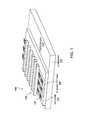
- FIG. 1is a perspective view of one embodiment of NAND flash type memory device 100 employing a junctionless transistor.
- the device 100can be fabricated on a semiconductor substrate 102 , or any other substrate.
- the substrate 102can be any semiconductor substrate known in the art, such as monocrystalline silicon, IV-IV compounds such as silicon-germanium or silicon carbide, III-V compounds, II-VI compounds, epitaxial layers over such substrates, or any other semiconducting or non-semiconducting material, such as glass, plastic, metal or ceramic substrate.
- the substratemay include integrated circuits fabricated thereon, such as CMOS driver circuits (CMOS circuits) and/or electrodes for the memory device.
- CMOS circuitsCMOS driver circuits
- FIG. 1a semiconductor-on-insulator (SOI) structure for a TFT type memory device is shown in FIG. 1 .
- the semiconductor substrate 102can be a p-type silicon substrate or n-type silicon substrate.
- CMOS driver circuits for controlling the memory device 100can also be built over or in the substrate 102 .
- An insulating layer 104such as a BOX oxide layer or another suitable insulating layer is formed over the substrate 102 .
- a plurality of junctionless semiconductor channel regions 106are formed over the insulating layer.
- the term “junctionless”means that the channel lacks a doped p-n junction in the boundary of the transistor. However, the channel may contain higher and lower doped regions of the same conductivity type.
- the channel regionsmay be made of any suitable semiconductor material, such as silicon, germanium, silicon-germanium, silicon carbide, III-V semiconductor materials, such as GaAs, GaN, etc., II-VI semiconductor materials, such as ZnSe, etc. Other semiconductor materials, such as semiconducting carbon nanotubes, may also be used.
- suitable semiconductor materialsuch as silicon, germanium, silicon-germanium, silicon carbide, III-V semiconductor materials, such as GaAs, GaN, etc., II-VI semiconductor materials, such as ZnSe, etc.
- Other semiconductor materialssuch as semiconducting carbon nanotubes, may also be used.
- the semiconductor materialmay be single crystalline, polycrystalline or amorphous.
- the semiconductor material 106is deposited as a amorphous silicon or polysilicon and then crystallized or recrystallized using thermal or laser annealing.
- the channels 106may be formed in a single crystal semiconductor substrate or in a single crystal layer directly on a surface of a single crystal substrate.
- the channels 106may be formed by depositing a semiconductor layer, followed by photolithographic patterning (e.g., masking and etching) of the layer into the elongated or strip shaped channels 106 .
- each channel 106comprises a semiconductor nanowire which is formed by photolithographic patterning described above or by growth on a separate substrate in nanowire form followed by transfer of the nanowire to the device substrate 102 .
- the semiconductor channelsare preferably narrow and can have two dimensions less than 100 nm.
- the channel 106can be a nanowire channel having a height of 2 to 20 nm, a width of 5 to 50 nm, a length larger than 50 nm, such as larger than 100 nm.
- the channels 106are preferably substantially uniformly doped (e.g., n or p-type doped) along their elongated direction.
- each channel 106is n or p-type doped to degeneracy.
- a degenerate semiconductoris a semiconductor with such a high doping level that the material starts to act more like a metal than as a semiconductor. At high enough impurity concentrations the individual impurity atoms may become close enough neighbors that their doping levels merge into an impurity band and the behavior of such a system ceases to show the typical traits of a semiconductor, e.g. its increase in conductivity with temperature. On the other hand, a degenerate semiconductor still has far fewer charge carriers than a true metal so that its behavior is in many ways intermediary between semiconductor and metal.
- the doping levelcan be at least 2 ⁇ 10 18 cm ⁇ 3 , or at least 1 ⁇ 10 19 cm ⁇ 3 , preferably in the range of 1-5 ⁇ 10 19 cm ⁇ 3 for n-type silicon (i.e., silicon doped with P, As and/or Sb).
- Each charge storage region 107comprises one of a dielectric isolated floating gate, an oxide-nitride-oxide charge trapping film (ONO CTF), or conductive nanodots, such as metal nanodots in an insulating matrix.
- O CTFoxide-nitride-oxide charge trapping film
- conductive nanodotssuch as metal nanodots in an insulating matrix.
- any suitable materialssuch as polysilicon, can be used so long as the work function of the floating gate allows electron injection, and the work function affects the threshold of the device.
- control gate electrodes 108are formed over the charge storage regions 107 and over the channels 106 .
- the control gate electrodesmay be made of any suitable conductive material, such as polysilicon or metal.
- the metal electrodescan comprise tungsten, copper, aluminum, tantalum, titanium, cobalt, titanium nitride or alloys thereof. In some embodiments, tungsten is preferred to allow processing under a relatively high temperature. In some other embodiments, copper or aluminum is a preferred material. Barrier and adhesion layers, such as TiN layers, may be included.
- the control gate materialis selected to have a work function that disfavors electron injection from the control gate.
- the NAND flash memory device 100includes at least one NAND string. For example, three adjacent NAND stings are shown. Each NAND string includes the junctionless, heavily doped semiconductor channel 106 , a plurality of control gate electrodes 108 adjacent to the channel, and one of a plurality of charge storage regions 107 located between the channel and each of the plurality of control gate electrodes. For example, as shown in FIG. 1 , each NAND string includes six control gates 108 .
- Each NAND stringcan be viewed as a plurality of junctionless thin film transistors containing a common junctionless nanowire channel 106 , and a charge storage region 107 between the channel 106 and each control gate 108 .
- the nanowire channellacks a doped p-n junction (i.e., source or drain diffusion).
- Such junctionless transistorsare also known as gated resistors.
- the channel 106has a nanoscale cross-sectional dimension such that a voltage on the order of about ⁇ 3 V to 3 V applied to a control gate electrode can deplete the free carriers or cause inversion in the channel. If the bias or electric field is absent in the channel, the channel can be conductive or “on.” Thus, the channel is gated (i.e., controlled by the gates) and can be switched between on and off states without the need for a diffusion junction.
- the memory device 100 of FIG. 1is a “horizontal” type, two dimensional NAND flash memory device.
- Each NAND stringis located substantially parallel to a major surface 103 of the substrate 102 .
- each channelis elongated in a direction parallel to this major surface 103 .
- the junctionless TFT structurecomprises depletion type (n+ body) cell transistors. Without the junctions and the resulting doping diffusion, short channel effects can be reduced, and the structure can be scaled to below 20 nm. As will be described below, three dimensional memory devices can also use the junctionless transistor in accordance with embodiments of the invention.
- each device levelincludes dopant ion implantation followed by the activation anneal.
- the activation anneal in each higher device levelnegatively affects the dopant distribution in the lower levels. With the junctionless devices, the activation anneals may be avoided.
- junctionless NAND flash memory devicesinclude, for example, low aspect ratio active area and control gate process, programming and reading being the same as conventional NAND flash memory, improved coupling ratio (e.g., a ratio of at least about 0.5), and n-body TFT NAND flash memory built in silicon on insulator (SOI).
- SOIsilicon on insulator
- the n-bodyis also advantageous for 3D vertical NAND integration, as will be described below. However, it is noted that because the erase potential drops along the n-type body, a modified erase operation may be needed.
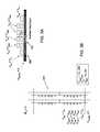
- FIG. 2A and 2Bare schematic diagrams illustrating a sequential erase operation in a memory device 200 .
- FIG. 2Ashows a cross-sectional view of a string of memory cells of a horizontal NAND device, such as that of FIG. 1 .
- FIG. 2Bshows a circuit schematic of a plurality (e.g., two) memory strings coupled together.
- the memory device 200comprises a first access gate electrode (also referred to as a selection gate electrode), such as a source side selection gate electrode 202 adjacent to one end (e.g., source side) of the channel 204 .
- the memory device 200can comprise a plurality of memory strings, as illustrated in FIG. 2B .
- the first access gate electrode 202can be located at the source end for selecting, for example, the plurality of control gate electrodes 208 .
- the plurality of control gate electrodes 208 having a common channel 218can be grouped into a plurality of strings.
- a second access gate electrode (e.g., drain selection gate electrode) 210can be located adjacent to another end (drain side) of the channel 204 .
- One of a plurality of charge storage regions 216is located between the channel 204 and each of the plurality of control gate electrodes 208 .
- No charge storage regionis located between the access gate electrodes 202 , 210 and the channel 204 .
- application of a voltage on the order of ⁇ 3 V to 3V to the channel 204may deplete the free carriers or cause inversion in the channel 204 , such as a depleted n+ body or inversion (hole) layers.
- the memory device 200further comprises a first contact 212 contacting the first end (source side) of the channel 204 adjacent to the first access gate electrode 202 , and a second contact 214 electrically contacting the second end (drain side) of the channel 204 adjacent to the second access gate electrode 210 .
- the first and second contacts 212 , 214can be made from a metal or a heavily doped n++ semiconductor layer.
- the NAND string of the memory device 200 as showncomprises a string of memory cells coupled to each other through the junctionless semiconductor channel 204 .
- V eraseerase voltage
- V erasemay be 5-20 V, such as 10-15 V.
- V CELSRCV erase
- FIGS. 2C and 2Dare schematic circuit diagrams illustrating exemplary erase sequences with positive voltages and negative voltages, respectively, for a NAND string 220 based on an n-type channel 240 .
- FIG. 2Cis a schematic diagram illustrating a variant of the sequential erase operation described above with respect to FIGS. 2A and 2B
- FIG. 2Dis a schematic diagram illustrating an alternative sequential erase operation described above with respect to FIGS. 2A and 2B
- the string 220includes a source line 222 , a source side selection (i.e., access) gate 224 , and control gate electrodes 226 for four cells 228 , 230 , 232 , 234 .
- V eraseis applied to the source line 222 and the source selection gate 224 .
- the first cell 228has a 0 volts applied to its control gate.
- the other cells 230 to 234have control gates that can be allowed to float.
- the first cell 228is erased, with the electrons stored in its storage region tunneling through the tunneling dielectric layer and into the channel 240 .
- the channel between the first cell 228 and the source line 222is “open” because the selection gate 224 has the V erase applied thereon as docs the source line 222 .
- the electrons injected from the storage region of the first cell 228can flow through the channel 240 to the source line 222 .
- source line 222 , the source selection gate 224 , and the control gate of the first cell 228have V erase applied thereon.
- the second cell 230has 0 V applied to its control gate while the remaining cells 232 , 234 control gates are allowed to float. In this case, the second cell 230 is erased.
- the V erasecan thus be sequentially applied to the cells 228 , 230 , . . . until the last cell in the string 220 is erased.
- the same sequencecan apply but the polarity of the voltages will change to negative.
- a p-type channelemits electrons in erase, and thus should be inverted under V erase .
- the doping concentrationshould not be much above the onset of degeneracy, i.e., the concentration should not be greater than about 10 19 cm ⁇ 3 .
- the method of FIG. 2Cincludes applying an erase voltage to a source line 222 of the NAND string 220 , applying at substantially the same time the erase voltage to a source side access gate 224 of the NAND string, and erasing a first memory cell 228 located adjacent to the source side access gate 224 by applying zero volts to a control gate 226 of the first memory cell 228 while allowing control gates 226 of remaining memory cells 230 - 234 of the NAND string 220 to float.
- the methodalso includes erasing a second memory cell 230 located adjacent to the first memory cell 228 by applying the erase voltage to a control gate 226 of the first memory cell 228 and applying zero volts to a control gate 226 of the second memory cell 230 while allowing control gates of remaining memory cells 232 , 234 of the NAND string to float.
- the methodfurther includes erasing a third memory cell 232 of the NAND string located adjacent to the second memory cell by applying the erase voltage to the control gates 226 of the first 228 and the second 230 memory cells, applying zero volts to the control gate 226 of the third memory cell 232 and letting the control gate of the last cell 234 float. The process is then repeated to erase the last cell 234 .
- the erase voltagecan be continuously applied or reapplied to the source line 222 of the NAND string and to the source side access gate 224 of the NAND string during the steps of erasing the first, the second, the third and the fourth memory cells 228 - 234 .
- the erase voltagecomprises a positive voltage (e.g., 10 to 20V) for an n-type doped channel or a negative voltage (e.g., ⁇ 10 to ⁇ 20V) for a p-type doped channel.
- unselected blockshave their source select gate held at a low voltage, e.g., less than 4 V while common array source electrode rises to the high positive voltage V erase . Therefore the select gate oxide must be sufficiently thick to withstand the ensuing high voltage stress over successive erase operations and cycles without degradation.
- FIG. 2Dan alternative sequential erase method is shown.
- a negative voltage ⁇ V eraseis applied to the control gate of cell 234 adjacent to the drain select gate 242 .
- the drain select gate 242has a voltage of 1-2 V applied thereto.
- the channel and the source select gate 224has 0 V applied thereto.
- the other cells 230 , 228 , 232have 0 V applied to their control gates.
- the cell 234is erased.
- ⁇ V eraseis applied to the control gate of cell 232 , while the other cells 228 , 230 , 234 and the source select gate 224 have 0 V applied thereon.
- cell 232is erased.
- the NAND string 220can thus be sequentially erased from the drain side. For a p-type substrate, the polarity of the voltage will be reversed while the sequence remains the same.
- the erase methodincludes applying zero volts to the channel, applying zero volts to a source side access gate 224 , applying a voltage of, e.g., 1 to 2V, to a drain side access gate 242 of the NAND string, erasing a first memory cell 234 located adjacent to the drain side access gate 242 by applying an erase voltage to a control gate of the first memory cell 234 while applying zero volts to control gates of remaining memory cells 228 - 232 of the NAND string.
- the methodalso includes erasing a second memory cell 232 of the NAND string located adjacent to the first memory cell 234 by applying an erase voltage to a control gate of the second memory cell 232 while applying zero volts to control gates of remaining memory cells 228 , 230 , 234 of the NAND string.
- the methodalso includes erasing a third memory cell 230 located adjacent to the second memory cell 232 by applying an erase voltage to a control gate of the third memory cell while applying zero volts to control gates of remaining memory cells 228 , 232 , 234 .
- the fourth memory cell 228can be erased using the same method as described above.
- the zero voltsis applied or reapplied to the channel and to the source side access gate of the NAND string and a voltage of 1-2 V is applied or reapplied to the drain side access gate of the NAND string during the steps of erasing the first, the second and the third memory cells.
- the erase voltagecomprises a negative voltage for an n-type doped channel or a positive voltage for a p-type doped channel.
- an erase-verify operationcan be applied to the row that was just erased.
- the erase-verify operationcan be, for example, reading the row of memory cells. Once successful erase in the row is verified, the next row is erased and then verified. If the row does not pass the erase-verify, the row alone can be erased again, for example, by being pulsed again to a higher voltage. This advantageously can save time as compared with the erase-verify process in conventional NAND memory devices, where erase-verify is performed after the erase operation has been applied to a whole block of memory cells.
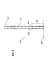
- FIGS. 3A and 3Bare schematic diagrams illustrating a word line erase operation (e.g., a random single word line erase operation) in a memory device 300 .
- the single word line processcan possibly be used for both erase and programming.
- a positive V erasecan be used if the channel is p-type rather than n-type as shown. This method is especially suited for devices with nanodot charge storage regions. Further, as above, a voltage applied to the channel 204 may deplete the free carriers or cause inversion in the channel 204 , such as an inversion (hole) layer in a n+body.
- FIG. 4is a cross-sectional view of a monolithic, three dimensional NAND memory device 400 which contains horizontal NAND strings in each device level.
- an insulating layersuch as an oxide layer 404 can be formed on a major surface of a substrate 402 .
- a semiconductor layercan be formed over the oxide layer 406 , and is then patterned into elongated highly n-doped TFT channel areas 406 , which can have a nanowire shape and extend substantially parallel to the major surface of the substrate 402 .
- a tunnel dielectric layer 408such as a silicon oxide layer can be formed over the channel 406 .
- a plurality of charge storage regions 410can be formed over the tunneling dielectric layer 408 .
- Regions 410may comprise metal floating gates or conductive nanodots. Regions 410 and layer 408 may be patterned into discrete regions using photolithographic patterning.
- an undercut 412is formed in the channel 406 using the plurality of charge storage regions 410 as a mask, thereby narrowing the width of the channel 406 relative to the storage region 410 .
- the undercutmay be formed by selective wet etching using a liquid etching medium which selectively etches the semiconductor material of the channel 406 over that of the dielectric layer 408 or the charge storage regions 410 .
- the undercuthas a width of 2-15 nm, such as 2-10 nm.
- An overhang portion 414 of each of the plurality of charge storage regions 408therefore overhangs the channel 406 .
- a blocking dielectric layer 416such as a silicon oxide layer, is then formed over the plurality of charge storage regions 410 , such that the blocking dielectric layer 416 fills a space (i.e., the undercut) 412 below the overhanging portion 414 of each of the plurality of charge storage regions 410 and the tunneling dielectric layer 408 .
- a plurality of control gates 418can then be formed over the blocking dielectric layer 416 by depositing a conductive layer and pattering it into gate strips, as shown in FIG. 1 . This completes the first device level 421 .
- Each device levelincludes one or more horizontal NAND strings parallel to the major surface of the substrate 402 .
- a narrowed width of the n-doped TFT channelhelps the channel to become depleted completely, thereby improving the coupling ratio.
- the coupling ratio of the devicecan be, for example, at least 0.5.
- Prior art nanodot flash memory devices or thin metal sheet floating gate memory devicessuffer from low program/erase window due to a low coupling ratio.
- a shallow trench isolation (STI) fillsuch as a silicon oxide fill, can be formed over the floating gates and filling the undercut areas.
- the control gate layer 418can then be formed over the STI layer 416 .
- FIG. 5is a schematic circuit diagram of a vertical, stacked, three dimensional junctionless NAND memory device 500 comprising a plurality of NAND strings 502 located substantially perpendicular to a major surface 504 of a substrate.
- the channel 506 of the strings 502in this case extends substantially perpendicular to the major surface 504 of the substrate.
- the plurality of control gate electrodes 508are also stacked in a direction substantially perpendicular to the major surface 504 of the substrate.
- the plurality of strings 502 as shown in FIG. 5are stacked in the direction substantially perpendicular to the major surface 504 of the substrate.
- Each of the plurality of NAND strings 502comprises the channel 506 which extends substantially perpendicular to the major surface 504 of the substrate, the plurality of control gate electrodes 508 which are stacked in the direction substantially perpendicular to the major surface 504 of a substrate, and access gate electrodes 510 adjacent to each respective end of the channel 506 .
- a gateless semiconductor (e.g., n-type polysilicon) transfer region 512can be located between adjacent ends of channels of adjacent NAND strings 502 .
- the two stings 502 adjacent to the major surface 504 of the substratecan be connected thereby forming a longer string.
- junctionless memory devices in accordance with embodiments of the inventioncan employ heavily doped n-type body, thereby solving the problems when the p-type body is used.
- a transistorIn a junctionless NAND memory device, individual memory cells are connected to the bitline (metal line) through other memory cells of the NAND string. Thus, overall string conductance is limited by the conductivity of cell regions between adjacent gate stacks, and the channels cannot be easily turned on by voltage applied on unselected wordlines in read, V read .
- a transistorIn comparison, a transistor usually has its source and drain connected to a metal line, so the resistance of the connecting path from the transistor channel to the metal line can be minimized by proper device and circuit layout.
- MOSFETs in logic and analog circuitsare designed not to emit electrons in surrounding dielectric layers during their normal operation.
- NAND cellsare required to emit electrons to and from charge storage nodes such as the floating gate, nanodot, or charge storage layers. These emitted electrons may accumulate over program/erase cycles in dielectric layers between gate stacks, causing string current degradation.
- design considerations in accordance with embodiments of the inventioninclude the doping level in the channels. If the doping were too low, the NAND string is likely difficult to erase and can be prone to erase degradation after program/erase cycling, due to the low conductivity associated with the low doping and the resulting difficulty in electrically coupling neighboring cells.
- the heavily doped channel throughout the entire string, including the regions in between gate stacks,allows the NAND string to erase more easily, with less cycling-induced degradation.
- the memory devicemay comprise a so-called resistivity switching non-volatile memory device (also referred to sometimes as a ReRAM device).
- An exemplary deviceis shown in FIG. 6 .
- a non-volatile memory cell 600includes a junctionless transistor 610 steering element located in series with the storage element 618 .
- the transistor 610 and the storage element 618are disposed between two electrodes 601 and 602 .
- the resistivity switching materialcomprises at least one of a fuse, antifuse dielectric, switchable metal oxide (e.g., nickel or vanadium oxide), complex metal oxide layer, carbon nanotube material, graphene resistivity switchable material, carbon resistivity switchable material, phase change material, conductive bridge element, or switchable polymer material.
- switchable metal oxidee.g., nickel or vanadium oxide
- complex metal oxide layercarbon nanotube material, graphene resistivity switchable material, carbon resistivity switchable material, phase change material, conductive bridge element, or switchable polymer material.
- FIG. 6illustrates the perspective view of a memory cell formed according to an embodiment of the present invention.
- a bottom conductor 601is formed of a conductive material, for example tungsten, and extends in a first direction. Barrier and adhesion layers, such as TiN layers, may be included in bottom conductor 601 .
- the junctionless transistor 610contains a junctionless channel in a shape of a nanowire extending perpendicular to the bottom conductor 601 .
- the channel ends 112 , 116are visible in FIG. 6 .
- the middle portion of the channelis covered by a circular wrap control gate 114 .
- the resistivity switching layer 618is disposed over or below the transistor 610 .
- Top conductor 602may be formed in the same manner and of the same materials as bottom conductor 601 , and extends in a second direction different from the first direction.
- the transistor 610is vertically disposed between bottom conductor 601 and top conductor 602 .
- the transistor and the storage elementmay have a cylindrical shape as illustrated in FIG. 6 , or a shape other than cylindrical.
- a design of a resistivity switching memory cellcomprising a diode and a metal oxide, see for example U.S. patent application Ser. No. 11/125,939 filed on May 9, 2005 (which corresponds to US Published Application No. 2006/0250836 to Herner et al.), and U.S. patent application Ser. No. 11/395,995 filed on Mar. 31, 2006 (which corresponds to US Patent Published Application No. 2006/0250837 to Herner et al.), each of which is hereby incorporated by reference.
- the above described memory cell shown in FIG. 6may be located in a one memory level device. If desired, additional memory levels can be formed above the first memory level to form a monolithic three dimensional memory array. In some embodiments, conductors can be shared between memory levels; i.e. top conductor 602 shown in FIG. 6 would serve as the bottom conductor of the next memory level. In other embodiments, an interlevel dielectric is formed above the first memory level, its surface planarized, and construction of a second memory level begins on this planarized interlevel dielectric, with no shared conductors.
- a monolithic three dimensional memory arrayis one in which multiple memory levels are formed above a single substrate, such as a wafer, with no intervening substrates.
- the layers forming one memory levelare deposited or grown directly over the layers of an existing level or levels.
- stacked memorieshave been constructed by forming memory levels on separate substrates and adhering the memory levels atop each other, as in Leedy, U.S. Pat. No. 5,915,167, “Three dimensional structure memory.”
- the substratesmay be thinned or removed from the memory levels before bonding, but as the memory levels are initially formed over separate substrates, such memories are not true monolithic three dimensional memory arrays.
- a monolithic three dimensional memory array formed above a substratecomprises at least a first memory level formed at a first height above the substrate and a second memory level formed at a second height different from the first height. Three, four, eight, or indeed any number of memory levels can be formed above the substrate in such a multilevel array.
Landscapes
- Engineering & Computer Science (AREA)
- Microelectronics & Electronic Packaging (AREA)
- Chemical & Material Sciences (AREA)
- Nanotechnology (AREA)
- Physics & Mathematics (AREA)
- Mathematical Physics (AREA)
- Theoretical Computer Science (AREA)
- Crystallography & Structural Chemistry (AREA)
- Non-Volatile Memory (AREA)
- Semiconductor Memories (AREA)
Abstract
Description
| T | ||||
| step | 1 | 2 | 3 | 4 |
| 0 | 0 | 0 | 0 | |
| 0 | 0 | 0 | Verase | |
| VCG | 0 | 0 | Verase | Verase |
| VCG | 0 | Verase | Verase | Verase |
| TABLE II | |||
| Vsgd | Von | ||
| VCGn+2 | Vpass | ||
| YCGn+1 | Vpass | ||
| VCGn | −Verase | ||
| VCGn−1 | Vpass | ||
| Vsgs | Von | ||
Claims (2)
Priority Applications (7)
| Application Number | Priority Date | Filing Date | Title |
|---|---|---|---|
| US12/848,458US8395942B2 (en) | 2010-05-17 | 2010-08-02 | Junctionless TFT NAND flash memory |
| CN201180024699XACN102893382A (en) | 2010-05-17 | 2011-04-29 | Memory device including junctionless thin film transistors |
| JP2013511180AJP2013531881A (en) | 2010-05-17 | 2011-04-29 | Memory device including junctionless thin film transistor |
| EP11718635AEP2572371A1 (en) | 2010-05-17 | 2011-04-29 | Memory device comprising a junctionless thin- film transistor |
| PCT/US2011/034517WO2011152938A1 (en) | 2010-05-17 | 2011-04-29 | Memory device comprising a junctionless thin- film transistor |
| KR1020127032579AKR101795826B1 (en) | 2010-05-17 | 2011-04-29 | Memory device comprising a junctionless thin-film transistor |
| TW100117253ATW201203524A (en) | 2010-05-17 | 2011-05-17 | Junctionless TFT NAND flash memory |
Applications Claiming Priority (2)
| Application Number | Priority Date | Filing Date | Title |
|---|---|---|---|
| US34535210P | 2010-05-17 | 2010-05-17 | |
| US12/848,458US8395942B2 (en) | 2010-05-17 | 2010-08-02 | Junctionless TFT NAND flash memory |
Publications (2)
| Publication Number | Publication Date |
|---|---|
| US20110280076A1 US20110280076A1 (en) | 2011-11-17 |
| US8395942B2true US8395942B2 (en) | 2013-03-12 |
Family
ID=44911655
Family Applications (1)
| Application Number | Title | Priority Date | Filing Date |
|---|---|---|---|
| US12/848,458Expired - Fee RelatedUS8395942B2 (en) | 2010-05-17 | 2010-08-02 | Junctionless TFT NAND flash memory |
Country Status (7)
| Country | Link |
|---|---|
| US (1) | US8395942B2 (en) |
| EP (1) | EP2572371A1 (en) |
| JP (1) | JP2013531881A (en) |
| KR (1) | KR101795826B1 (en) |
| CN (1) | CN102893382A (en) |
| TW (1) | TW201203524A (en) |
| WO (1) | WO2011152938A1 (en) |
Cited By (26)
| Publication number | Priority date | Publication date | Assignee | Title |
|---|---|---|---|---|
| US20130248956A1 (en)* | 2012-03-20 | 2013-09-26 | Samsung Electronics Co., Ltd. | Semiconductor devices and methods of manufacturing the same |
| US20130272069A1 (en)* | 2012-04-13 | 2013-10-17 | Sandisk Technologies Inc. | 3d non-volatile storage with transistor decoding structure |
| WO2015108742A1 (en) | 2014-01-15 | 2015-07-23 | Apple Inc. | Improved storage in charge-trap memory structures using additional electrically-charged regions |
| US9240420B2 (en) | 2013-09-06 | 2016-01-19 | Sandisk Technologies Inc. | 3D non-volatile storage with wide band gap transistor decoder |
| US9419115B2 (en) | 2014-11-10 | 2016-08-16 | International Business Machines Corporation | Junctionless tunnel fet with metal-insulator transition material |
| US10559563B2 (en) | 2017-06-26 | 2020-02-11 | Taiwan Semiconductor Manufacturing Co., Ltd. | Method for manufacturing monolithic three-dimensional (3D) integrated circuits |
| US11069696B2 (en) | 2018-07-12 | 2021-07-20 | Sunrise Memory Corporation | Device structure for a 3-dimensional NOR memory array and methods for improved erase operations applied thereto |
| WO2022046219A1 (en)* | 2020-08-31 | 2022-03-03 | Sandisk Technologies Llc | Read time reduction with p-well bias in memory device |
| US11302406B2 (en) | 2015-09-30 | 2022-04-12 | Sunrise Memory Corporation | Array of nor memory strings and system for rapid data retrieval |
| US11387364B2 (en) | 2020-11-03 | 2022-07-12 | Globalfoundries U.S. Inc. | Transistor with phase transition material region between channel region and each source/drain region |
| US11488676B2 (en) | 2015-09-30 | 2022-11-01 | Sunrise Memory Corporation | Implementing logic function and generating analog signals using NOR memory strings |
| US11705496B2 (en) | 2020-04-08 | 2023-07-18 | Sunrise Memory Corporation | Charge-trapping layer with optimized number of charge-trapping sites for fast program and erase of a memory cell in a 3-dimensional NOR memory string array |
| US11729980B2 (en) | 2017-06-20 | 2023-08-15 | Sunrise Memory Corporation | 3-dimensional NOR memory array architecture and methods for fabrication thereof |
| US11730000B2 (en) | 2017-06-20 | 2023-08-15 | Sunrise Memory Corporation | 3-dimensional nor string arrays in segmented stacks |
| US11749344B2 (en) | 2015-09-30 | 2023-09-05 | Sunrise Memory Corporation | Three-dimensional vertical nor flash thin-film transistor strings |
| US11751388B2 (en) | 2017-06-20 | 2023-09-05 | Sunrise Memory Corporation | 3-dimensional nor strings with segmented shared source regions |
| US11758727B2 (en) | 2018-02-02 | 2023-09-12 | Sunrise Memory Corporation | Three-dimensional vertical nor flash thin-film transistor strings |
| US11817156B2 (en) | 2015-09-30 | 2023-11-14 | Sunrise Memory Corporation | Multi-gate nor flash thin-film transistor strings arranged in stacked horizontal active strips with vertical control gates |
| US11839086B2 (en) | 2021-07-16 | 2023-12-05 | Sunrise Memory Corporation | 3-dimensional memory string array of thin-film ferroelectric transistors |
| US11844217B2 (en) | 2018-12-07 | 2023-12-12 | Sunrise Memory Corporation | Methods for forming multi-layer vertical nor-type memory string arrays |
| US11842777B2 (en) | 2020-11-17 | 2023-12-12 | Sunrise Memory Corporation | Methods for reducing disturb errors by refreshing data alongside programming or erase operations |
| US11844204B2 (en) | 2019-12-19 | 2023-12-12 | Sunrise Memory Corporation | Process for preparing a channel region of a thin-film transistor in a 3-dimensional thin-film transistor array |
| US11848056B2 (en) | 2020-12-08 | 2023-12-19 | Sunrise Memory Corporation | Quasi-volatile memory with enhanced sense amplifier operation |
| US12073082B2 (en) | 2020-02-07 | 2024-08-27 | Sunrise Memory Corporation | High capacity memory circuit with low effective latency |
| US12183834B2 (en) | 2020-01-22 | 2024-12-31 | Sunrise Memory Corporation | Cool electron erasing in thin-film storage transistors |
| US12402319B2 (en) | 2021-09-14 | 2025-08-26 | Sunrise Memory Corporation | Three-dimensional memory string array of thin-film ferroelectric transistors formed with an oxide semiconductor channel |
Families Citing this family (41)
| Publication number | Priority date | Publication date | Assignee | Title |
|---|---|---|---|---|
| US9406574B1 (en)* | 2007-08-09 | 2016-08-02 | Cypress Semiconductor Corporation | Oxide formation in a plasma process |
| US20190067109A1 (en)* | 2011-06-28 | 2019-02-28 | Monolithic 3D Inc. | 3d semiconductor device and system |
| US10497713B2 (en)* | 2010-11-18 | 2019-12-03 | Monolithic 3D Inc. | 3D semiconductor memory device and structure |
| JP5271372B2 (en)* | 2011-03-18 | 2013-08-21 | 株式会社東芝 | Manufacturing method of semiconductor device |
| US8742481B2 (en) | 2011-08-16 | 2014-06-03 | Micron Technology, Inc. | Apparatuses and methods comprising a channel region having different minority carrier lifetimes |
| CN102544073A (en)* | 2011-12-16 | 2012-07-04 | 北京大学深圳研究生院 | Knot-free nanowire field effect transistor |
| JP2014013634A (en)* | 2012-07-03 | 2014-01-23 | Toshiba Corp | Nonvolatile semiconductor memory device and operation method thereof |
| KR20140029024A (en) | 2012-08-31 | 2014-03-10 | 에스케이하이닉스 주식회사 | Junctionless semiconductor device having buried gate, module and system having the device and manufacturing method of the device |
| KR102091713B1 (en) | 2012-09-27 | 2020-03-20 | 삼성전자 주식회사 | Non-volatile memory device and fabricating method thereof |
| TWI524825B (en) | 2012-10-29 | 2016-03-01 | 財團法人工業技術研究院 | Method of transferring carbon conductive film |
| US8984463B2 (en) | 2012-11-28 | 2015-03-17 | Qualcomm Incorporated | Data transfer across power domains |
| US9064077B2 (en)* | 2012-11-28 | 2015-06-23 | Qualcomm Incorporated | 3D floorplanning using 2D and 3D blocks |
| US8988941B2 (en) | 2012-12-18 | 2015-03-24 | SanDisk Tehcnologies Inc. | Select transistor tuning |
| CN103915342B (en)* | 2013-01-08 | 2016-08-31 | 中芯国际集成电路制造(上海)有限公司 | Nodeless mesh body pipe and the forming method of complementary nodeless mesh body pipe |
| US8877586B2 (en) | 2013-01-31 | 2014-11-04 | Sandisk 3D Llc | Process for forming resistive switching memory cells using nano-particles |
| US9536840B2 (en) | 2013-02-12 | 2017-01-03 | Qualcomm Incorporated | Three-dimensional (3-D) integrated circuits (3DICS) with graphene shield, and related components and methods |
| US9041448B2 (en) | 2013-03-05 | 2015-05-26 | Qualcomm Incorporated | Flip-flops in a monolithic three-dimensional (3D) integrated circuit (IC) (3DIC) and related methods |
| US9177890B2 (en) | 2013-03-07 | 2015-11-03 | Qualcomm Incorporated | Monolithic three dimensional integration of semiconductor integrated circuits |
| US9171608B2 (en) | 2013-03-15 | 2015-10-27 | Qualcomm Incorporated | Three-dimensional (3D) memory cell separation among 3D integrated circuit (IC) tiers, and related 3D integrated circuits (3DICS), 3DIC processor cores, and methods |
| WO2014162018A1 (en)* | 2013-04-05 | 2014-10-09 | University College Cork - National University Of Ireland, Cork | Junctionless nanowire transistors for 3d monolithic integration of cmos inverters |
| CN104701321B (en)* | 2013-12-09 | 2017-12-08 | 旺宏电子股份有限公司 | Integrated circuit with memory array and method of operating the same |
| CN103972300B (en)* | 2014-05-14 | 2015-09-30 | 京东方科技集团股份有限公司 | A kind of thin-film transistor and preparation method thereof, array base palte, display unit |
| US9484086B2 (en) | 2014-07-10 | 2016-11-01 | Sandisk Technologies Llc | Determination of word line to local source line shorts |
| US9443612B2 (en) | 2014-07-10 | 2016-09-13 | Sandisk Technologies Llc | Determination of bit line to low voltage signal shorts |
| US9460809B2 (en)* | 2014-07-10 | 2016-10-04 | Sandisk Technologies Llc | AC stress mode to screen out word line to word line shorts |
| US9613973B2 (en)* | 2014-10-03 | 2017-04-04 | Micron Technology, Inc. | Memory having a continuous channel |
| CN105514110B (en)* | 2014-10-15 | 2018-01-05 | 国家纳米科学中心 | A kind of nonvolatile memory based on single more wall carbon pipes and preparation method thereof |
| CN104462729B (en)* | 2014-12-31 | 2018-04-03 | 中国电子科技集团公司第四十七研究所 | A kind of layout method of antifuse series on-site programmable gate array |
| US9659963B2 (en)* | 2015-06-29 | 2017-05-23 | International Business Machines Corporation | Contact formation to 3D monolithic stacked FinFETs |
| KR101802055B1 (en)* | 2016-02-16 | 2017-11-27 | 한국과학기술원 | Vertically integrated gate-all-around multiple nanowire junctionless transistor and manufacturing method thereof |
| US9660107B1 (en)* | 2016-08-31 | 2017-05-23 | Taiwan Semiconductor Manufacturing Co., Ltd. | 3D cross-bar nonvolatile memory |
| CN107887262B (en)* | 2016-09-30 | 2020-01-14 | 中芯国际集成电路制造(北京)有限公司 | Semiconductor device and method for manufacturing the same |
| KR101852424B1 (en)* | 2016-10-07 | 2018-04-27 | 재단법인 다차원 스마트 아이티 융합시스템 연구단 | The method for enhancing the driving current of junctionless transistor |
| CN108257968A (en)* | 2016-12-28 | 2018-07-06 | 上海新昇半导体科技有限公司 | A kind of no pn junction p n trench gate array memory structure and preparation method thereof |
| CN108257961A (en)* | 2016-12-28 | 2018-07-06 | 上海新昇半导体科技有限公司 | A kind of grid array is without pn junction p n channel transistor structure structure and preparation method thereof |
| CN108305877B (en)* | 2017-01-13 | 2020-09-25 | 上海新昇半导体科技有限公司 | A gate-last junctionless NAND flash memory and method of making the same |
| US11367731B2 (en)* | 2017-11-24 | 2022-06-21 | Taiwan Semiconductor Manufacturing Company Ltd. | Memory device and method of manufacturing the same |
| KR102071363B1 (en) | 2018-07-30 | 2020-01-30 | 고려대학교 산학협력단 | Junctionless Field Effect Transistor with Metal-Interlayer-Semiconductor Structure and Method thereof |
| US11164890B2 (en)* | 2020-01-09 | 2021-11-02 | Sandisk Technologies Llc | Cross-point array of ferroelectric field effect transistors and method of making the same |
| JP2022181756A (en) | 2021-05-27 | 2022-12-08 | ウィンボンド エレクトロニクス コーポレーション | semiconductor storage device |
| JP7074417B1 (en)* | 2021-06-16 | 2022-05-24 | ウィンボンド エレクトロニクス コーポレーション | Semiconductor storage device |
Citations (12)
| Publication number | Priority date | Publication date | Assignee | Title |
|---|---|---|---|---|
| US5677556A (en) | 1993-06-29 | 1997-10-14 | Kabushiki Kaisha Toshiba | Semiconductor device having inversion inducing gate |
| US5915167A (en) | 1997-04-04 | 1999-06-22 | Elm Technology Corporation | Three dimensional structure memory |
| US20060250836A1 (en) | 2005-05-09 | 2006-11-09 | Matrix Semiconductor, Inc. | Rewriteable memory cell comprising a diode and a resistance-switching material |
| US20060278913A1 (en) | 2005-06-08 | 2006-12-14 | Micron Technology, Inc. | Non-volatile memory cells without diffusion junctions |
| US20090321830A1 (en) | 2006-05-15 | 2009-12-31 | Carnegie Mellon University | Integrated circuit device, system, and method of fabrication |
| EP2161755A1 (en) | 2008-09-05 | 2010-03-10 | University College Cork-National University of Ireland, Cork | Junctionless Metal-Oxide-Semiconductor Transistor |
| US7679960B2 (en)* | 2006-12-22 | 2010-03-16 | Samsung Elecronics Co., Ltd. | Non-volatile memory device and method of operating the same |
| US7701780B2 (en)* | 2007-05-31 | 2010-04-20 | Micron Technology, Inc. | Non-volatile memory cell healing |
| US7812404B2 (en) | 2005-05-09 | 2010-10-12 | Sandisk 3D Llc | Nonvolatile memory cell comprising a diode and a resistance-switching material |
| US8017991B2 (en)* | 2006-07-28 | 2011-09-13 | Samsung Electronics Co., Ltd. | Non-volatile memory device and methods of operating and fabricating the same |
| US8114757B1 (en)* | 2010-10-11 | 2012-02-14 | Monolithic 3D Inc. | Semiconductor device and structure |
| US8203148B2 (en)* | 2010-10-11 | 2012-06-19 | Monolithic 3D Inc. | Semiconductor device and structure |
- 2010
- 2010-08-02USUS12/848,458patent/US8395942B2/ennot_activeExpired - Fee Related
- 2011
- 2011-04-29KRKR1020127032579Apatent/KR101795826B1/enactiveActive
- 2011-04-29CNCN201180024699XApatent/CN102893382A/enactivePending
- 2011-04-29WOPCT/US2011/034517patent/WO2011152938A1/enactiveApplication Filing
- 2011-04-29JPJP2013511180Apatent/JP2013531881A/ennot_activeWithdrawn
- 2011-04-29EPEP11718635Apatent/EP2572371A1/ennot_activeWithdrawn
- 2011-05-17TWTW100117253Apatent/TW201203524A/enunknown
Patent Citations (13)
| Publication number | Priority date | Publication date | Assignee | Title |
|---|---|---|---|---|
| US5677556A (en) | 1993-06-29 | 1997-10-14 | Kabushiki Kaisha Toshiba | Semiconductor device having inversion inducing gate |
| US5915167A (en) | 1997-04-04 | 1999-06-22 | Elm Technology Corporation | Three dimensional structure memory |
| US7812404B2 (en) | 2005-05-09 | 2010-10-12 | Sandisk 3D Llc | Nonvolatile memory cell comprising a diode and a resistance-switching material |
| US20060250836A1 (en) | 2005-05-09 | 2006-11-09 | Matrix Semiconductor, Inc. | Rewriteable memory cell comprising a diode and a resistance-switching material |
| US20060278913A1 (en) | 2005-06-08 | 2006-12-14 | Micron Technology, Inc. | Non-volatile memory cells without diffusion junctions |
| US20090321830A1 (en) | 2006-05-15 | 2009-12-31 | Carnegie Mellon University | Integrated circuit device, system, and method of fabrication |
| US8017991B2 (en)* | 2006-07-28 | 2011-09-13 | Samsung Electronics Co., Ltd. | Non-volatile memory device and methods of operating and fabricating the same |
| US7679960B2 (en)* | 2006-12-22 | 2010-03-16 | Samsung Elecronics Co., Ltd. | Non-volatile memory device and method of operating the same |
| US7701780B2 (en)* | 2007-05-31 | 2010-04-20 | Micron Technology, Inc. | Non-volatile memory cell healing |
| EP2161755A1 (en) | 2008-09-05 | 2010-03-10 | University College Cork-National University of Ireland, Cork | Junctionless Metal-Oxide-Semiconductor Transistor |
| US8178862B2 (en)* | 2008-09-05 | 2012-05-15 | University College Cork, National University Of Ireland Cork | Junctionless metal-oxide-semiconductor transistor |
| US8114757B1 (en)* | 2010-10-11 | 2012-02-14 | Monolithic 3D Inc. | Semiconductor device and structure |
| US8203148B2 (en)* | 2010-10-11 | 2012-06-19 | Monolithic 3D Inc. | Semiconductor device and structure |
Non-Patent Citations (7)
| Title |
|---|
| Colinge, Jean-Pierre, "Nanowire Transistors Without Junctions", Nature Nanotechnology, pp. 1-5, Feb. 21, 2010. |
| Colinge, Jean-Pierre, et al. "Nanowire Transistors Without Junctions"; Nature Nanotechnology, vol. 5, No. 3, Mar. 1, 2010. |
| Huang, Po-Chun, et al. "Eletric-Field Enhancement of a Gate-All-Around Nanowire Thin-Film Transistor Memory"; IEEE Electron Device Letters, vol. 31, No. 3, Mar. 2010. |
| International Search Report issued in PCT Application PCT/US2011/034517, mailed on Sep. 20, 2011. |
| U.S. Appl. No. 11/125,939, filed May 9, 2005. |
| U.S. Appl. No. 11/395,995, filed Mar. 31, 2006. |
| Weis, Marcus, et al. "Stacked 3-Dimensional 6T SRAM Cell with Independent Double Gate Transistors"; IC Design and Technology; IEEE International Conference-May 18, 2009. |
Cited By (41)
| Publication number | Priority date | Publication date | Assignee | Title |
|---|---|---|---|---|
| US8686485B2 (en)* | 2012-03-20 | 2014-04-01 | Samsung Electronics Co., Ltd. | Semiconductor devices and methods of manufacturing the same |
| US20140179073A1 (en)* | 2012-03-20 | 2014-06-26 | Samsung Electronics Co., Ltd. | Semiconductor devices and methods of manufacturing the same |
| US8980736B2 (en)* | 2012-03-20 | 2015-03-17 | Samsung Electronics Co., Ltd. | Semiconductor devices and methods of manufacturing the same |
| US20130248956A1 (en)* | 2012-03-20 | 2013-09-26 | Samsung Electronics Co., Ltd. | Semiconductor devices and methods of manufacturing the same |
| US9406781B2 (en) | 2012-04-13 | 2016-08-02 | Sandisk Technologies Llc | Thin film transistor |
| US20130272069A1 (en)* | 2012-04-13 | 2013-10-17 | Sandisk Technologies Inc. | 3d non-volatile storage with transistor decoding structure |
| US8865535B2 (en) | 2012-04-13 | 2014-10-21 | Sandisk Technologies Inc. | Fabricating 3D non-volatile storage with transistor decoding structure |
| US8923048B2 (en)* | 2012-04-13 | 2014-12-30 | Sandisk Technologies Inc. | 3D non-volatile storage with transistor decoding structure |
| US9123420B2 (en) | 2012-04-13 | 2015-09-01 | Sandisk Technologies Inc. | 3D non-volatile storage with transistor decoding structure |
| US9129681B2 (en) | 2012-04-13 | 2015-09-08 | Sandisk Technologies Inc. | Thin film transistor |
| US9240420B2 (en) | 2013-09-06 | 2016-01-19 | Sandisk Technologies Inc. | 3D non-volatile storage with wide band gap transistor decoder |
| US9312017B2 (en) | 2014-01-15 | 2016-04-12 | Apple Inc. | Storage in charge-trap memory structures using additional electrically-charged regions |
| US9672925B2 (en) | 2014-01-15 | 2017-06-06 | Apple Inc. | Storage in charge-trap memory structures using additional electrically-charged regions |
| WO2015108742A1 (en) | 2014-01-15 | 2015-07-23 | Apple Inc. | Improved storage in charge-trap memory structures using additional electrically-charged regions |
| US9419115B2 (en) | 2014-11-10 | 2016-08-16 | International Business Machines Corporation | Junctionless tunnel fet with metal-insulator transition material |
| US9419016B2 (en) | 2014-11-10 | 2016-08-16 | International Business Machines Corporation | Junctionless tunnel FET with metal-insulator transition material |
| US11749344B2 (en) | 2015-09-30 | 2023-09-05 | Sunrise Memory Corporation | Three-dimensional vertical nor flash thin-film transistor strings |
| US11915768B2 (en) | 2015-09-30 | 2024-02-27 | Sunrise Memory Corporation | Memory circuit, system and method for rapid retrieval of data sets |
| US11817156B2 (en) | 2015-09-30 | 2023-11-14 | Sunrise Memory Corporation | Multi-gate nor flash thin-film transistor strings arranged in stacked horizontal active strips with vertical control gates |
| US12002523B2 (en) | 2015-09-30 | 2024-06-04 | Sunrise Memory Corporation | Memory circuit, system and method for rapid retrieval of data sets |
| US11302406B2 (en) | 2015-09-30 | 2022-04-12 | Sunrise Memory Corporation | Array of nor memory strings and system for rapid data retrieval |
| US11488676B2 (en) | 2015-09-30 | 2022-11-01 | Sunrise Memory Corporation | Implementing logic function and generating analog signals using NOR memory strings |
| US11508445B2 (en) | 2015-09-30 | 2022-11-22 | Sunrise Memory Corporation | Capacitive-coupled non-volatile thin-film transistor strings in three dimensional arrays |
| US11751388B2 (en) | 2017-06-20 | 2023-09-05 | Sunrise Memory Corporation | 3-dimensional nor strings with segmented shared source regions |
| US11729980B2 (en) | 2017-06-20 | 2023-08-15 | Sunrise Memory Corporation | 3-dimensional NOR memory array architecture and methods for fabrication thereof |
| US11730000B2 (en) | 2017-06-20 | 2023-08-15 | Sunrise Memory Corporation | 3-dimensional nor string arrays in segmented stacks |
| US10559563B2 (en) | 2017-06-26 | 2020-02-11 | Taiwan Semiconductor Manufacturing Co., Ltd. | Method for manufacturing monolithic three-dimensional (3D) integrated circuits |
| US11758727B2 (en) | 2018-02-02 | 2023-09-12 | Sunrise Memory Corporation | Three-dimensional vertical nor flash thin-film transistor strings |
| US12245430B2 (en) | 2018-02-02 | 2025-03-04 | Sunrise Memory Corporation | Three-dimensional vertical nor flash thin-film transistor strings |
| US11069696B2 (en) | 2018-07-12 | 2021-07-20 | Sunrise Memory Corporation | Device structure for a 3-dimensional NOR memory array and methods for improved erase operations applied thereto |
| US11844217B2 (en) | 2018-12-07 | 2023-12-12 | Sunrise Memory Corporation | Methods for forming multi-layer vertical nor-type memory string arrays |
| US11844204B2 (en) | 2019-12-19 | 2023-12-12 | Sunrise Memory Corporation | Process for preparing a channel region of a thin-film transistor in a 3-dimensional thin-film transistor array |
| US12183834B2 (en) | 2020-01-22 | 2024-12-31 | Sunrise Memory Corporation | Cool electron erasing in thin-film storage transistors |
| US12073082B2 (en) | 2020-02-07 | 2024-08-27 | Sunrise Memory Corporation | High capacity memory circuit with low effective latency |
| US11705496B2 (en) | 2020-04-08 | 2023-07-18 | Sunrise Memory Corporation | Charge-trapping layer with optimized number of charge-trapping sites for fast program and erase of a memory cell in a 3-dimensional NOR memory string array |
| WO2022046219A1 (en)* | 2020-08-31 | 2022-03-03 | Sandisk Technologies Llc | Read time reduction with p-well bias in memory device |
| US11387364B2 (en) | 2020-11-03 | 2022-07-12 | Globalfoundries U.S. Inc. | Transistor with phase transition material region between channel region and each source/drain region |
| US11842777B2 (en) | 2020-11-17 | 2023-12-12 | Sunrise Memory Corporation | Methods for reducing disturb errors by refreshing data alongside programming or erase operations |
| US11848056B2 (en) | 2020-12-08 | 2023-12-19 | Sunrise Memory Corporation | Quasi-volatile memory with enhanced sense amplifier operation |
| US11839086B2 (en) | 2021-07-16 | 2023-12-05 | Sunrise Memory Corporation | 3-dimensional memory string array of thin-film ferroelectric transistors |
| US12402319B2 (en) | 2021-09-14 | 2025-08-26 | Sunrise Memory Corporation | Three-dimensional memory string array of thin-film ferroelectric transistors formed with an oxide semiconductor channel |
Also Published As
| Publication number | Publication date |
|---|---|
| KR20130119327A (en) | 2013-10-31 |
| US20110280076A1 (en) | 2011-11-17 |
| JP2013531881A (en) | 2013-08-08 |
| CN102893382A (en) | 2013-01-23 |
| TW201203524A (en) | 2012-01-16 |
| EP2572371A1 (en) | 2013-03-27 |
| KR101795826B1 (en) | 2017-11-08 |
| WO2011152938A1 (en) | 2011-12-08 |
Similar Documents
| Publication | Publication Date | Title |
|---|---|---|
| US8395942B2 (en) | Junctionless TFT NAND flash memory | |
| US12293794B2 (en) | Multi-gate nor flash thin-film transistor strings arranged in stacked horizontal active strips with vertical control gates | |
| US11456297B2 (en) | Semiconductor memory device, method of driving the same and method of fabricating the same | |
| US9893076B2 (en) | Access transistor of a nonvolatile memory device and method for fabricating same | |
| US11683935B2 (en) | NOR flash memory | |
| JP4601287B2 (en) | Nonvolatile semiconductor memory device | |
| CN1677675B (en) | Nonvolatile semiconductor memory device | |
| US9343152B2 (en) | Cell array with a manufacturable select gate for a nonvolatile semiconductor memory device | |
| KR20220133333A (en) | Three-dimensional vertical nor flash thin-film transistor strings | |
| US20160086970A1 (en) | Three-dimensional non-volatile nor-type flash memory | |
| US20160049421A1 (en) | Three dimensional nand device having dummy memory holes and method of making thereof | |
| US20120008400A1 (en) | Non-volatile semiconductor storage device and method of manufacturing the same | |
| US20080128780A1 (en) | Non-volatile semiconductor storage device | |
| KR20080032025A (en) | TF charge storage memory cell with highly mobile corrugated channel | |
| KR101073640B1 (en) | High-density vertical-type semiconductor memory cell string, cell string array and fabricating method thereof | |
| US20080191263A1 (en) | Nonvolatile memory devices and methods of fabricating the same | |
| US12254915B1 (en) | Integrated circuit structure and method for forming and operating the same | |
| KR20090006097A (en) | Semiconductor Field Effect Transistors, Memory Cells, and Memory Devices |
Legal Events
| Date | Code | Title | Description |
|---|---|---|---|
| AS | Assignment | Owner name:SANDISK CORPORATION, CALIFORNIA Free format text:ASSIGNMENT OF ASSIGNORS INTEREST;ASSIGNORS:SAMACHISA, GEORGE;ALSMEIER, JOHANN;MIHNEA, ANDREI;REEL/FRAME:025538/0629 Effective date:20100729 | |
| AS | Assignment | Owner name:SANDISK TECHNOLOGIES INC., TEXAS Free format text:ASSIGNMENT OF ASSIGNORS INTEREST;ASSIGNOR:SANDISK CORPORATION;REEL/FRAME:026259/0144 Effective date:20110404 | |
| STCF | Information on status: patent grant | Free format text:PATENTED CASE | |
| AS | Assignment | Owner name:SANDISK TECHNOLOGIES LLC, TEXAS Free format text:CHANGE OF NAME;ASSIGNOR:SANDISK TECHNOLOGIES INC;REEL/FRAME:038807/0850 Effective date:20160516 | |
| FPAY | Fee payment | Year of fee payment:4 | |
| MAFP | Maintenance fee payment | Free format text:PAYMENT OF MAINTENANCE FEE, 8TH YEAR, LARGE ENTITY (ORIGINAL EVENT CODE: M1552); ENTITY STATUS OF PATENT OWNER: LARGE ENTITY Year of fee payment:8 | |
| FEPP | Fee payment procedure | Free format text:MAINTENANCE FEE REMINDER MAILED (ORIGINAL EVENT CODE: REM.); ENTITY STATUS OF PATENT OWNER: LARGE ENTITY | |
| LAPS | Lapse for failure to pay maintenance fees | Free format text:PATENT EXPIRED FOR FAILURE TO PAY MAINTENANCE FEES (ORIGINAL EVENT CODE: EXP.); ENTITY STATUS OF PATENT OWNER: LARGE ENTITY | |
| STCH | Information on status: patent discontinuation | Free format text:PATENT EXPIRED DUE TO NONPAYMENT OF MAINTENANCE FEES UNDER 37 CFR 1.362 | |
| FP | Lapsed due to failure to pay maintenance fee | Effective date:20250312 |