US8395935B2 - Cross-point self-aligned reduced cell size phase change memory - Google Patents
Cross-point self-aligned reduced cell size phase change memoryDownload PDFInfo
- Publication number
- US8395935B2 US8395935B2US12/899,232US89923210AUS8395935B2US 8395935 B2US8395935 B2US 8395935B2US 89923210 AUS89923210 AUS 89923210AUS 8395935 B2US8395935 B2US 8395935B2
- Authority
- US
- United States
- Prior art keywords
- memory
- memory array
- region
- programmable
- phase change
- Prior art date
- Legal status (The legal status is an assumption and is not a legal conclusion. Google has not performed a legal analysis and makes no representation as to the accuracy of the status listed.)
- Active, expires
Links
Images


Classifications
- H—ELECTRICITY
- H10—SEMICONDUCTOR DEVICES; ELECTRIC SOLID-STATE DEVICES NOT OTHERWISE PROVIDED FOR
- H10B—ELECTRONIC MEMORY DEVICES
- H10B63/00—Resistance change memory devices, e.g. resistive RAM [ReRAM] devices
- H10B63/30—Resistance change memory devices, e.g. resistive RAM [ReRAM] devices comprising selection components having three or more electrodes, e.g. transistors
- H—ELECTRICITY
- H10—SEMICONDUCTOR DEVICES; ELECTRIC SOLID-STATE DEVICES NOT OTHERWISE PROVIDED FOR
- H10B—ELECTRONIC MEMORY DEVICES
- H10B63/00—Resistance change memory devices, e.g. resistive RAM [ReRAM] devices
- H10B63/10—Phase change RAM [PCRAM, PRAM] devices
- H—ELECTRICITY
- H10—SEMICONDUCTOR DEVICES; ELECTRIC SOLID-STATE DEVICES NOT OTHERWISE PROVIDED FOR
- H10B—ELECTRONIC MEMORY DEVICES
- H10B63/00—Resistance change memory devices, e.g. resistive RAM [ReRAM] devices
- H10B63/80—Arrangements comprising multiple bistable or multi-stable switching components of the same type on a plane parallel to the substrate, e.g. cross-point arrays
- G—PHYSICS
- G11—INFORMATION STORAGE
- G11C—STATIC STORES
- G11C13/00—Digital stores characterised by the use of storage elements not covered by groups G11C11/00, G11C23/00, or G11C25/00
- G11C13/0002—Digital stores characterised by the use of storage elements not covered by groups G11C11/00, G11C23/00, or G11C25/00 using resistive RAM [RRAM] elements
- G11C13/0004—Digital stores characterised by the use of storage elements not covered by groups G11C11/00, G11C23/00, or G11C25/00 using resistive RAM [RRAM] elements comprising amorphous/crystalline phase transition cells
Definitions
- This inventionrelates to high density memory devices based on phase change memory materials, including chalcogenide based materials, and on other programmable resistance materials, and methods for manufacturing such devices.
- Phase change based memory materialssuch as chalcogenide based materials and similar materials, can be caused to change phase between an amorphous state and a crystalline state by application of electrical current at levels suitable for implementation in integrated circuits.
- the generally amorphous stateis characterized by higher electrical resistivity than the generally crystalline state, which can be readily sensed to indicate data.
- the change from the amorphous to the crystalline stateis generally a lower current operation.
- the change from crystalline to amorphous, referred to as reset herein,is generally a higher current operation, which includes a short high current density pulse to melt or breakdown the crystalline structure, after which the phase change material cools quickly, quenching the phase change process and allowing at least a portion of the phase change material to stabilize in the amorphous state.
- the magnitude of the current needed for resetcan be reduced by reducing the size of the phase change material element in the cell and/or the contact area between electrodes and the phase change material, such that higher current densities are achieved with small absolute current values through the phase change material element.
- a cross-point programmable memory arrayin which the programmable memory cells are aligned at the access devices and at the cross-points of the bit lines and the word lines.
- a layer of peripheral logic devicesis formed at the surface of the semiconductor substrate body and the programmable memory elements are formed over the surface of the semiconductor substrate body, so that a plane defined by the peripheral logic gates intersects the programmable memory elements.
- a method for making the memory arrayemploys a damascene process in forming one or both the bit lines and the word lines; and the bit line is (or both the bit line and the word line are) self-aligned with the access devices and the programmable memory elements.
- the bit linesare defined in the substrate between first isolation structures formed in trenches parallel to the bit line direction.
- Second isolation structuresare formed in trenches parallel to the word line direction, shallower than the first isolation trenches.
- the first and second isolation structuresextend above the semiconductor surface.
- the memory cell access devicesare formed in the semiconductor substrate, and they are confined in one direction between the first isolation structures and in a perpendicular direction between the second isolation structures.
- the word lines and the programmable memory elementsare formed in word line trenches overlying the memory cell access devices, and are confined between the first isolation structures above the semiconductor substrate surface. As a result, the programmable memory elements and the access devices and the bit lines are all “self-aligned”.
- a hard maskis used to define the second (word line) isolation trenches, and this hard mask can be left in place until the programmable memory elements and the word lines are to be formed; in these embodiments a fill can be formed over the second isolation trenches, and portions of the hard mask overlying the memory cell access devices can be selectively removed to form the word line trenches.
- the word lines, the programmable memory elements and the access devicesare all “self-aligned”.
- the word lines and the programmable memory elementsare “self-aligned” (they are formed in the word line trench by a damascene process), but the word lines and programmable memory elements are not self-aligned with the memory cell access devices.
- a method for making the memory arrayemploys a damascene process in forming one or both the bit lines and the word lines; and the bit line is (or both the bit line and the word line are) self-aligned with the access devices and the programmable memory elements.
- the inventionfeatures a programmable memory device including a semiconductor substrate body having a surface including a periphery region and a memory array region, the device including a programmable memory array in the memory array region and a layer of logic devices at the substrate surface in the periphery region, the memory array including access devices formed in the substrate body and programmable memory elements formed over the substrate surface, in which the access devices and memory elements are aligned at cross-points of bit lines and word lines, and the bit lines are self-aligned with the programmable memory elements and the access devices.
- the word linesare self-aligned with the programmable memory elements and the access devices.
- the inventionfeatures a programmable memory device including a semiconductor substrate body having a surface including a periphery region and a memory array region, the device including a programmable memory array in the memory array region and a layer of logic devices at the substrate surface in the periphery region, the memory array including access devices formed in the substrate body and programmable memory elements formed over the substrate surface, in which a plane defined by peripheral logic gates intersects the programmable memory elements.
- the access devices and memory elementsare aligned at cross-points of bit lines and word lines, and the bit lines are self-aligned with the programmable memory elements and the access devices.
- the word linesare self-aligned with the programmable memory elements and the access devices.
- the inventionfeatures a method for making a programmable memory array, by: providing a semiconductor substrate having a surface overlying a memory array region and a periphery region; depositing a gate oxide layer and a gate layer over the substrate surface; forming first trench isolation structures parallel to a first direction using a common mask over both the memory array region and the periphery region; removing the common mask and forming a silicon nitride layer over the gate layer and the first trench isolation structures; forming second trenches parallel to a second direction perpendicular to the first direction; forming a dielectric fill over the memory array region; patterning the periphery gate oxide layer and gate layer using a logic mask over the periphery region to form logic gates; performing a device implant in the periphery region to form source and drain regions; forming a dielectric fill over the memory array region and the periphery region and planarizing the dielectric fill; removing the silicon nitride layer and the gate layer and gate oxide layer over the memory
- the inventionfeatures a method for making a programmable memory array, by: providing a semiconductor substrate having a surface overlying a memory array region and a periphery region; depositing a gate oxide layer and a gate layer over the substrate surface; forming first trench isolation structures parallel to a first direction using a common mask over both the memory array region and the periphery region; removing the common mask and forming second trenches parallel to a second direction perpendicular to the first direction; forming a dielectric fill over the memory array region; patterning the periphery gate oxide layer and gate layer using a logic mask over the periphery region to form logic gates; performing a device implant in the periphery region to form source and drain regions; forming a dielectric fill over the memory array region and the periphery region and planarizing the dielectric fill; removing the gate layer and gate oxide layer over the memory array to form word line trenches; forming spacers on the first and second trench isolation structures in the memory array region to form pores;
- the methodfurther includes one or more of: following forming the second trenches, forming a first memory array salicide; prior to forming the dielectric fill over the memory array region and the periphery region, forming a peripheral region salicide; prior to forming the spacers in the memory array region, forming a second memory array salicide.
- the methodfurther includes forming memory access device implants at one or more stages: prior to depositing the gate oxide layer over the substrate surface, following forming the second trenches, prior to forming spacers in the memory array region. In some embodiments the method further includes forming peripheral device implants in the substrate underlying the peripheral region at one or more stages: prior to depositing the gate oxide layer over the substrate surface, following forming the logic gates.
- forming the second trenchesincludes forming a mask over the silicon nitride layer and, using the mask, etching to form the second trenches.
- forming the memory cellsincludes depositing a programmable memory material over the second memory array salicide in the word line trenches and forming a top electrode over the programmable memory material. In some embodiments forming the memory cells includes depositing a bottom electrode material over the second memory array salicide in the word line trenches, depositing a programmable memory material over the bottom electrode material, and forming a top electrode over the programmable memory material.
- forming memory cells over the second memory array salicideincludes forming a mask over the memory array region and the periphery region, patterned to form word line trenches overlying the second memory array salicide; and depositing a programmable memory material and a top electrode in the word line trenches.
- forming the memory cellsincludes depositing a programmable memory material over the second memory array salicide and forming a top electrode over the programmable memory material. In some embodiments forming the memory cells includes depositing a bottom electrode material over the second memory array salicide, depositing a programmable memory material over the bottom electrode material, and forming a top electrode over the programmable memory material.
- the methodfurther includes, following forming memory cells, forming a passivation layer over the memory array region and the periphery region; and forming contacts through the passivation layer to top electrodes in the memory array region and to source/drain regions in the periphery region.
- memory cells in the memory arrayhave an area equal to 4D 2 , where D is about one half the sum of the word line width and the separation distance between word lines, typically about the minimum feature size for a lithographic process used in manufacturing the memory cells.
- the structurecan be formed using a self-aligned process in which the word lines and memory elements are aligned with the vertical transistors without additional patterning steps. Also, the memory material is not exposed to etching chemistry during processing, leaving the memory elements damage free.
- the disclosed methodsprovide a memory array of cells having reduced cell size, and the methods have a low processing cost, as a reduced number of masks are required.
- FIG. 1is a flow diagram outlining stages in a process for making a phase change memory according to an embodiment.
- FIGS. 2A , 2 B, 2 Care diagrammatic sketches showing a phase change memory according to an embodiment.
- FIG. 2Ais a plan view
- FIG. 2Bis a transverse sectional view as indicated at B-B in FIG. 2A
- FIG. 2Cis a transverse sectional view as indicated at C-C in FIG. 2A .
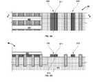
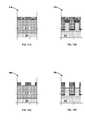
- FIGS. 3 , 4 , 5 A, 5 B, 6 A, 6 B, 6 C, 7 A, 7 B, 7 C, 7 D, 7 E, 8 A, 8 B, 8 C, 8 D, 8 E, 9 A, 9 B, 10 A, 10 B, 11 A, 11 B, 11 C, 11 D, 12 A, 12 B, 12 C, 12 D, 13 A, 13 B, 13 C, 13 D, 14 A, 14 B, 14 C, 14 D, 15 A, 15 B, 16 A, 16 B, 17are diagrammatic sketches showing stages in a process for making a phase change memory according to an embodiment.
- FIG. labeled A(for example, 7 A) is a plan view
- a FIG. labeled Bis a transverse sectional view as indicated at B-B in the corresponding plan view
- a FIG. labeled C, D, or Eis a transverse sectional view as indicated at C-C, D-D, or E-E, in a corresponding view.
- FIG. 7Bis a transverse sectional view as indicated at B-B in FIG. 7A
- FIG. 7Cis a transverse sectional view as indicated at C-C in FIG. 7A
- FIG. 7Dis a transverse sectional view as indicated at D-D in FIGS. 7A and 7B
- FIG. 7Eis a transverse sectional view as indicated at E-E in FIGS. 7A and 7C .
- FIG. 18is a flow diagram outlining stages in a process for making a phase change memory according to another embodiment.
- FIGS. 19A , 19 B, 19 C, 20 A, 20 B, 21 A, 21 B, 22 A, 22 B, 23 A, 23 B, 24 A, 24 B, 25 A, 25 B, 26 A, 26 B, 26 C, 27 A, 27 B, 28 A, 28 B,are diagrammatic sketches showing stages in a process for making a phase change memory according to an embodiment. (The various views are identified according the scheme outlined above.)
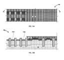
- FIGS. 29 , 30are diagrammatic sketches in sectional view illustrating examples of embodiments.
- FIG. 31is a schematic diagram for a memory array implemented using memory cells as described herein.
- FIG. 32is a simplified block diagram of an integrated circuit including an array of memory cells having access devices and memory elements as described herein.
- FIG. 31is a schematic illustration of a memory array 310 , which can be implemented using memory cells as described herein.
- each memory cell 317includes a diode access device 318 and a programmable resistance memory element 316 (represented as a variable resistor) arranged in series along a current path between a corresponding word line 312 and a corresponding bit line 314 .
- the memory element in a given memory cellis programmable to a plurality of resistance states including a first and a second resistance state.
- the arraycomprises a plurality of word lines 312 including word lines 312 a , 312 b , and 312 c extending in parallel in a first direction, and a plurality of bit lines 314 including bit lines 314 a , 314 b , and 314 c extending in parallel in a second direction perpendicular to the first direction.
- the array 310is referred to as a cross-point array because the word lines 312 and bit lines 314 cross each other but do not physically intersect, and the memory cells 317 are located at these cross-point locations of the word lines 312 and bit lines 314 .
- Memory cell 317is representative of the memory cells of array 310 and is arranged at the cross-point location of the word line ′ 312 b and the bit line 314 b , the memory cell 317 including (in this example) a diode 318 and a memory element 316 arranged in series.
- the diode 318is electrically coupled to the word line 312 b and the memory element 316 is electrically coupled to the bit line 314 b.
- Reading or writing to memory cell 317 of array 310can be achieved by applying appropriate voltage pulses to the corresponding word line 312 b and bit line 314 b to induce a current through the selected memory cell 317 .
- the level and duration of the voltages appliedis dependent upon the operation performed, e.g., a reading operation or a programming operation.
- bias circuitryIn a read (or sense) operation of the data value stored in the memory cell 317 , bias circuitry (see, e.g., biasing arrangement supply voltages, current sources 3236 of FIG. 32 ) coupled to the corresponding word line 312 b and bit line 314 b to apply bias arrangements across the memory cell 317 of suitable amplitude and duration to induce current to flow which does not result in the memory element 316 undergoing a change in resistive state.
- the current through the memory cell 317is dependent upon the resistance of the memory element 316 and, thus, upon the data value stored in the memory cell 317 .
- the data valuemay be determined, for example, by comparison of the current on the bit line 314 b with a suitable reference current by sense amplifiers (see, e.g., sense amplifiers/data in structures 3224 of FIG. 32 ).
- bias circuitryIn a program operation of a data value to be stored in the memory cell 317 , bias circuitry (see, e.g., biasing arrangement supply voltages, current sources 3236 of FIG. 32 ) coupled to the corresponding word line 312 b and bit line 314 b to apply bias arrangements across the memory cell 317 of suitable amplitude and duration to induce a programmable change in the memory element 316 to store the data value in the memory cell 317 , the electrical resistance of the memory element 316 corresponding to the data value stored in the memory cell 317 .
- bias circuitrysee, e.g., biasing arrangement supply voltages, current sources 3236 of FIG. 32 ) coupled to the corresponding word line 312 b and bit line 314 b to apply bias arrangements across the memory cell 317 of suitable amplitude and duration to induce a programmable change in the memory element 316 to store the data value in the memory cell 317 , the electrical resistance of the memory element 316 corresponding to the data value stored in the memory cell 317
- the bias arrangementsinclude a first bias arrangement sufficient to forward bias the diode 318 and change the resistance state of the memory element 317 from a resistance corresponding to a first programmed state to a resistance corresponding to a second programmed state.
- the bias arrangementsalso include a second bias arrangement sufficient to forward bias the diode 318 and change the resistance state of the memory element 317 from a resistance corresponding to the second programmed state to a resistance corresponding to the first programmed state.
- the bias arrangements for unipolar operation of the memory element 317may each comprise one or more voltage pulses, and the voltage levels and pulse times can be determined empirically for each embodiment.
- FIG. 32is a simplified block diagram of an integrated circuit 3201 including a cross-point memory array 310 of memory cells.
- each memory cellincludes a diode access device and a programmable resistance memory element.
- a word line (row) decoder 3214is coupled to and in electrical communication with a plurality of word lines 3216 .
- a bit line (column) decoder 3218is in electrical communication with a plurality of bit lines 3220 to read data from, and write data to, the memory cells (not shown) in array 310 . Addresses are supplied on bus 3222 to word line decoder and devices 3214 and bit line decoder 3218 .
- Sense amplifiers and data-in structures in block 3224are coupled to bit line decoder 3218 via data bus 3226 .
- Dataare supplied via a data-in line 3228 from input/output ports on integrated circuit 3201 , or from other data sources internal or external to integrated circuit 3201 , to data-in structures in block 3224 .
- Other circuitry 3230may be included on integrated circuit 3201 , such as a general purpose processor or special purpose application circuitry, or a combination of modules providing system-on-a-chip functionality supported by array 310 .
- Dataare supplied via a data-out line 3232 from the sense amplifiers in block 3224 to input/output ports on integrated circuit 3201 , or to other data destinations internal or external to integrated circuit 3201 .
- Controller 3234may be implemented using special-purpose logic circuitry as known in the art.
- controller 3234comprises a general-purpose processor, which may be implemented on the same integrated circuit to execute a computer program to control the operations of the device.
- a combination of special-purpose logic circuitry and a general-purpose processormay be utilized for implementation of controller 3234 .
- Embodiments of the programmable resistance material of the memory material elementinclude phase change based memory materials, including chalcogenide based materials and other materials.
- Chalcogensinclude any of the four elements oxygen (O), sulfur (S), selenium (Se), and tellurium (Te), forming part of group VIA of the periodic table.
- Chalcogenidescomprise compounds of a chalcogen with a more electropositive element or radical.
- Chalcogenide alloyscomprise combinations of chalcogenides with other materials such as transition metals.
- a chalcogenide alloyusually contains one or more elements from group IVA of the periodic table of elements, such as germanium (Ge) and tin (Sn).
- chalcogenide alloysinclude combinations including one or more of antimony (Sb), gallium (Ga), indium (In), and silver (Ag).
- Sbantimony
- Gagallium
- Inindium
- silversilver
- phase change based memory materialsinclude alloys of: Ga/Sb, In/Sb, In/Se, Sb/Te, Ge/Te, Ge/Sb/Te, In/Sb/Te, Ga/Se/Te, Sn/Sb/Te, In/Sb/Ge, Ag/In/Sb/Te, Ge/Sn/Sb/Te, Ge/Sb/Se/Te and Te/Ge/Sb/S.
- compositionscan be workable.
- the compositionscan be characterized as Te a Ge b Sb 100-(a+b) .
- One researcherhas described the most useful alloys as having an average concentration of Te in the deposited materials well below 70%, typically below about 60% and ranged in general from as low as about 23% up to about 58% Te and most preferably about 48% to 58% Te.
- Concentrations of Gewere above about 5% and ranged from a low of about 8% to about 30% average in the material, remaining generally below 50%. Most preferably, concentrations of Ge ranged from about 8% to about 40%. The remainder of the principal constituent elements in this composition was Sb.
- a transition metalsuch as chromium (Cr), iron (Fe), nickel (Ni), niobium (Nb), palladium (Pd), platinum (Pt) and mixtures or alloys thereof may be combined with Ge/Sb/Te to form a phase change alloy that has programmable resistance properties.
- chromium (Cr)iron (Fe), nickel (Ni), niobium (Nb), palladium (Pd), platinum (Pt) and mixtures or alloys thereof
- Ge/Sb/TeGe/Sb/Te
- Specific examples of memory materials that may be usefulare given in Ovshinsky '112 at columns 11-13, which examples are hereby incorporated by reference.
- impuritiesmay be added to chalcogenides and other phase change materials in some embodiments to modify conductivity, transition temperature, melting temperature, and other properties of memory elements using the additive-modified chalcogenides.
- impurities used as additives for chalcogenidesinclude nitrogen, silicon, oxygen, silicon dioxide, silicon nitride, copper, silver, gold, aluminum, aluminum oxide, tantalum, tantalum oxide, tantalum nitride, titanium and titanium oxide. See, e.g., U.S. Pat. No. 6,800,504, and U.S. Patent Application Publication No. U.S. 2005/0029502.
- Phase change alloysare capable of being switched between a first structural state in which the material is in a generally amorphous solid phase, and a second structural state in which the material is in a generally crystalline solid phase in its local order in the active channel region of the cell. These alloys are at least bistable.
- amorphousis used to refer to a relatively less ordered structure, more disordered than a single crystal, which has the detectable characteristics such as higher electrical resistivity than the crystalline phase.
- crystallineis used to refer to a relatively more ordered structure, more ordered than in an amorphous structure, which has detectable characteristics such as lower electrical resistivity than the amorphous phase.
- phase change materialsmay be electrically switched between different detectable states of local order across the spectrum between completely amorphous and completely crystalline states.
- Other material characteristics affected by the change between amorphous and crystalline phasesinclude atomic order, free electron density and activation energy.
- the materialmay be switched either into different solid phases or into mixtures of two or more solid phases, providing a gray scale between completely amorphous and completely crystalline states.
- the electrical properties in the materialmay vary accordingly.
- Phase change alloyscan be changed from one phase state to another by application of electrical pulses. It has been observed that a shorter, higher amplitude pulse tends to change the phase change material to a generally amorphous state. A longer, lower amplitude pulse tends to change the phase change material to a generally crystalline state. The energy in a shorter, higher amplitude pulse is high enough to allow for bonds of the crystalline structure to be broken and short enough to prevent the atoms from realigning into a crystalline state. Appropriate profiles for pulses can be determined, without undue experimentation, specifically adapted to a particular phase change alloy. In following sections of the disclosure, the phase change material is referred to as GST, and it will be understood that other types of phase change materials can be used. A material useful for implementation of a PCRAM described herein is Ge 2 Sb 2 Te 5 .
- RRAMresistance random access memory
- metal-oxidesincluding tungsten-oxide (WO x ), NiO, Nb 2 O 5 , CuO 2 , Ta 2 O 5 , Al 2 O 3 , CoO, Fe 2 O 3 , HfO 2 , TiO 2 , SrTiO 3 , SrZrO 3 , (BaSr)TiO 3 .
- MRAMmagnetoresistance random access memory
- STTspin-torque-transfer
- Additional examplesinclude solid electrolyte materials used for programmable-metallization-cell (PMC) memory, or nano-ionic memory, such as silver-doped germanium sulfide electrolytes and copper-doped germanium sulfide electrolytes.
- PMCprogrammable-metallization-cell
- nano-ionic memorysuch as silver-doped germanium sulfide electrolytes and copper-doped germanium sulfide electrolytes.
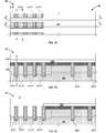
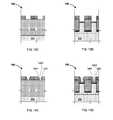
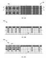
- FIGS. 2A , 2 B, 2 Cshow portions of a memory 20 including a memory cell array and of peripheral logic circuitry, in a plan view ( FIG. 2A ), and in sectional views ( FIGS. 2B , 2 C).
- the memory 20includes a memory region 2100 and a periphery region 2200 on the single-crystalline semiconductor substrate 202 .
- the substrate 202has a substantially planar top surface.
- the term “substantially planar”is intended to accommodate manufacturing tolerances during the formation of the substrate 202 .
- the term “substantially planar”is also intended to accommodate manufacturing processes performed following the formation of the substrate 202 which may cause variations in the planarity of the top surface.
- the periphery region 2200includes logic devices, isolated by trench isolations, for example trench isolation 2217 .
- Each logic devicesuch as logic device 2210 , for example, has a gate structure on a gate dielectric layer 2213 .
- the gate dielectric layer 2213is on the top surface of the substrate 202 .
- the gate structureincludes a layer 2211 of doped polysilicon on the gate dielectric layer 2213 , and a layer 2212 of silicide on the doped polysilicon.
- the logic device 2210includes doped regions 2214 , 2215 within the substrate 202 acting as the source and drain regions.
- a dielectric 206comprising one or more layers of dielectric material overlies the logic device 2210 . (The structure is presented in FIG. 2A as if the dielectric 206 were transparent, so that features beneath it can be seen.)
- Contact 2216is coupled to doped region 2215 and extends to the top surface of dielectric 206 where it can access overlying circuitry.
- the memory region 2100includes an array of access devices (not shown in these FIGs.; the position of one such device is suggested by the arrow 2111 ), formed in the single-crystalline silicon substrate 202 and isolated by trench isolations, for example trench isolations 2117 , 2117 ′, 2117 ′′, 2117 ′′′.
- a salicide layer 2114overlies the access devices at the surface of the substrate 202 overlying the access devices.
- the phase change memory cellsare constructed over the salicide layer at the top surface of the substrate 202 ; that is, the phase change memory cells are in the same layer (suggested by the bracket 2110 ) as the gate structures of the peripheral logic.
- phase change memory cell configurationsare contemplated (and some examples are described below); in the example shown in these FIGs., the memory material is a “pore structure”, including a horizontal portion 2113 and vertical portions 2112 ; the vertical portions are formed in pores in a surrounding dielectric layer 204 .
- the horizontal portion 2113 of the phase change memory material elementis overlain by a top electrode 2115 .
- Contact 2116is coupled to top electrode 2115 and extends to the top surface of dielectric 206 where it can access overlying circuitry.
- the bit lines 2115are designed to have a specified bit line width and to be separated by a specified first separation distance.
- the word linesare designed to have a specified word line width and to be separated by a specified second separation distance.
- the summation of the specified bit line width and the specified first separation distanceequals about twice a feature size D, wherein D is a nominal feature size for the lithographic process used to create the word lines and bit lines; and the summation of the specified word line width and the specified second separation distance equals about twice the feature size D.
- the memory cellhas an area 2500 equal to about 4D 2 .
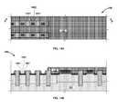
- FIG. 1is a flow diagram outlining stages in a process for making a phase change memory; and FIGS. 3-17 illustrate, in various views, stages in construction of a phase change memory according to an embodiment of the invention.
- a semiconductor substrate 202is provided; typically the substrate is a single-crystal silicon substrate, but other semiconductors are contemplated.
- a device implantis carried out in a memory array region 2100 and in a peripheral region 2200 of the semiconductor substrate ( FIG. 3 , at 30 ).
- First device implantsmay be performed at this stage: to form P or N wells for access devices in the memory array region, and P or N wells for peripheral logic devices in the peripheral region.
- One or more additional implantsmay be performed at this stage including: an implant to form bit lines in the memory array region (by, for example, a N+ implant where the well is P), and implants to form elements of diode access devices or transistor access devices (by, for example, a P implant over a N+ implant, to form a N-P diode; or a P implant over a N+ implant, followed by an additional shallow N+ implant).
- an implant to form bit lines in the memory array regionby, for example, a N+ implant where the well is P
- implants to form elements of diode access devices or transistor access devicesby, for example, a P implant over a N+ implant, to form a N-P diode; or a P implant over a N+ implant, followed by an additional shallow N+ implant.
- one or more device implantsmay be performed at one or more subsequent stages.
- Suitable access devicesinclude, for example, vertically-constructed devices, such as vertical diodes, vertical field effect transistors (FET), vertical bipolar junction transistors (BJT), vertical metal oxide semiconductors (MOS).
- vertically-constructed devicessuch as vertical diodes, vertical field effect transistors (FET), vertical bipolar junction transistors (BJT), vertical metal oxide semiconductors (MOS).
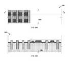
- a gate oxide layer 402is formed over the substrate surface in both the memory array region 2100 and in a peripheral region 2200 ; and in a subsequent stage a gate layer 404 is formed over the gate oxide layer 402 .
- a resultis shown at 40 in FIG. 4 .
- the gate oxide layer and the gate layerwill be patterned to form gate structures in the peripheral logic. Suitable materials for the gate layer include polysilicon, for example, and the gate layer may be formed by low-pressure chemical-vapor deposition, for example.
- first trench isolationsare formed in the memory array region (trench isolations 2117 ) and in the peripheral region (trench isolations 2217 ).
- a suitable technique for forming the trenchesresults in substantially planar, approximately vertical sidewalls, and may be carried out in two or more steps.
- Suitable techniques for forming the trenchinclude, for example, a directional etch such as, for example, an RIE.
- the RIEmay be controlled by selection of process parameters; employing lower pressure and higher substrate bias may provide better control of the shape and dimensions of the trench. Where RIE is employed, it may be followed by a cleaning process.
- a double-patterning or manifold patterning lithographic techniquemay be employed; examples of such techniques are outlined in Ping Xie et al. (2009) “Analysis of higher-order pitch division for sub-32 nm lithography”, Proc. of SPIE , Vol. 7274, pp. 72741Y-1 through 72741Y-8.
- the isolation trenches in both the periphery region and the memory array regionmay be patterned using a common (shared) mask.
- Suitable materials for filling the trenchesare dielectric, and suitable dielectric materials include, for example, oxides (e.g., silicon oxides, such as SiO 2 ) and nitrides (e.g., silicon nitrides, such as SiN); low-K dielectric materials (such as a doped SiO 2 , for example) may be preferred; and materials having low thermal conductivity may be preferred.
- the dielectriccan be formed by, for example, a physical vapor deposition (PVD) process, or a chemical vapor deposition (CVD) process.
- PVDphysical vapor deposition
- CVDchemical vapor deposition
- a planarizing stepby, for example, a chemical mechanical polish, CMP may be carried out following trench filling.
- a resultis shown at 50 in FIGS. 5A , 5 B.
- a silicon nitride layer 602is formed over the structure resulting from trench isolation. Suitable techniques for forming the silicon nitride layer include low pressure chemical vapor deposition, for example.
- the silicon nitrideis patterned in a subsequent step, and the patterned silicon nitride serves as a hard mask for trench formation (see below). Materials other than silicon nitride, suitable for use as a hard mask, may be used to form this layer.
- a resultis shown at 60 in FIGS. 6A , 6 B, 6 C.
- second trenchesare formed in the memory array region, using a mask-and etch procedure to form patterned trenches through the SiN and through selected underlying layers.
- the mask for patterning the hard mask layer (silicon nitride) in this stepis not shown in the FIGs.
- Suitable techniques for forming the second trenchesinclude techniques that selectively remove the unmasked SiN 602 , the unmasked gate material 504 , the unmasked gate oxide material 502 , and the unmasked semiconductor substrate 202 material; but do not remove the dielectric fill in the first trench isolations.
- the etchmay be carried out in more than one step, using etch techniques and/or etch parameters suitable for the various materials being etched.
- Suitable techniques for forming the trenchinclude, for example, a directional etch such as, for example an RIE.
- the RIEmay be controlled by selection of process parameters; employing lower pressure and higher substrate bias may provide better control of the shape and dimensions of the trench.
- a double-patterning or manifold patterning lithographic techniquemay be employed; examples of such techniques are outlined in Ping Xie et al. (2009), cited above.
- the final stage of the etchmay be timed, to establish an etch stop at the bottom of the trench.
- a resultis shown at 70 in FIGS. 7A , 7 B, 7 C.
- a memory array device implantationmay be carried out.
- the memory array implantmust be carried out before formation of the silicon nitride mask.
- a salicide 820is formed on the memory array; and a dielectric fill 840 is formed.
- suitable materials for filling the trenchesare dielectric, and suitable dielectric materials include, for example, oxides (e.g., silicon oxides, such as SiO 2 ) and nitrides (e.g., silicon nitrides, such as SiN); low-K dielectric materials (such as a doped SiO 2 , for example) may be preferred; and materials having low thermal conductivity may be preferred.
- the dielectriccan be formed by, for example, a physical vapor deposition (PVD) process, or a chemical vapor deposition (CVD) process.
- a planarizing step(by, for example, a chemical mechanical polish, CMP) may be carried out following trench filling.
- a resultis shown at 80 in FIGS. 8A , 8 B, 8 C.
- logic gatese.g., 910 , 910 ′
- Each patterned gateincludes a gate structure 911 stacked over a gate oxide 913 .
- a resultis shown at 90 in FIGS. 9A , 9 B. Suitable materials for the logic gate mask and suitable techniques for etching, that remove unmasked gate material but do not remove the isolation structures, are known.
- the strips 920 of SiN remaining over the memory array regionprotect the gate and gate oxide that overlies the memory cell devices.
- a peripheral device implantationis carried out to form source and drain regions, and thereafter in the peripheral region dielectric spacers are formed adjacent the gate stacks ( 1001 ) and at exposed surfaces of the dielectric trench isolation structures ( 1002 ). Thereafter a salicide 1010 is formed on exposed areas of the substrate adjacent the spacers and on the exposed surfaces of the gates. A result is shown at 110 in FIGS. 10A , 10 B.
- the peripheral regionis filled with a dielectric 112 and the resulting structure is planarized, for example by CMP.
- Suitable materials for the dielectricinclude, for example, oxides (e.g., silicon oxides, such as SiO 2 ) and nitrides (e.g., silicon nitrides, such as SiN); low-K dielectric materials (such as a doped SiO 2 , for example) may be preferred; and materials having low thermal conductivity may be preferred.
- the dielectric support layercan be formed by, for example, a physical vapor deposition (PVD) process, or a chemical vapor deposition (CVD) process. A result is shown at 110 in FIGS. 11A , 11 B.
- a subsequent stage 112the gate oxide layer and silicon oxide layer are removed from the memory array region, by for example a selective etch.
- a resultis shown in FIGS. 12A , 12 B.
- an additional memory array implantmay be carried out, optionally followed by a salicide, e.g. salicide 1302 .
- a resultis shown at 130 in FIGS. 13A , 13 B.
- oxide spacersare formed on oxide sidewalls in the memory array region, with a result as shown for example at 140 in FIGS. 14A , 14 B, 14 C, 14 D.
- the oxide spacerse.g., spacers 1401
- This small contact areais, as a result of the process, aligned (“self-aligned”) with the underlying access device, and also will be aligned with the intersection of the word and bit lines, as described below.
- phase change material 1502is deposited over the memory array region, filling in the openings over the small contact areas of exposed salicide.
- a chalcogenide materialis employed.
- the chalcogenide material filmmay be formed by vapor deposition, such as physical vapor deposition (PVD) or chemical vapor deposition (CVD), for example.
- PVDphysical vapor deposition
- CVDchemical vapor deposition
- An example of a method for forming a chalcogenide material filmuses a PVD-sputtering or magnetron-sputtering method with source gas(es) of Ar, N 2 , and/or He, etc. at the pressure in the range 1 mTorr ⁇ 100 mTorr.
- the depositionis usually done at room temperature.
- a collimator with an aspect ratio of 1 ⁇ 5can be used to improve the fill-in performance.
- a DC bias of several tens of volts to several hundreds of voltsmay also be used.
- the combination of DC bias and the collimatorcan be used simultaneously.
- Another example of a method for forming a chalcogenide material filmuses CVD such as that disclosed in U.S. Patent Application Publication No. 2006/0172067, titled “Chemical Vapor Deposition of Chalcogenide Materials”, which is incorporated by reference herein.
- Suitable materials for the top electrodeinclude conductive materials such as a metal or metal-based material or a non-metal material, such as, e.g.: copper; aluminum; titanium (Ti) and titanium-based materials such as titanium nitride (TiN), titanium ox nitride (TON); tantalum (Ta) and tantalum-based materials such as tantalum nitride (TaN); polysilicon, tungsten-based materials such as tungsten silicide (WSi x ); and, for a low thermal conductivity electrode, materials such as LNO (LaNiO3) and LSMO (LaSrMnO 3 ).
- conductive materialssuch as a metal or metal-based material or a non-metal material, such as, e.g.: copper; aluminum; titanium (Ti) and titanium-based materials such as titanium nitride (TiN), titanium ox nitride (TON); tantalum (Ta) and tantalum-based materials
- the top electrode layermay be formed by any of a variety of techniques suited to the particular material. Such techniques include, by way of example, sputtering and plating and CVD.
- the top electrodemay have a thickness, for example, in a range about 200 ⁇ to about 5000 ⁇ , usually about 2000 ⁇ .
- a post-deposition annealing treatment in a vacuum or in an N 2 ambientis optionally performed to improve the crystalline state of chalcogenide material.
- the annealing temperaturetypically ranges from 100° C. to 400° C. with an anneal time of less than 30 minutes.
- a dielectric coatingfor example of borophosphosilicate glass (BPSG) is formed over the structure, and the BPSG is planarized.
- contactsare formed to couple structures in the memory array and in the periphery to the top surface of the structure.
- Contact 2616is coupled to doped region 2615 and extends to the top surface of dielectric 206 where it can access overlying circuitry.
- Contact 1616is coupled to top electrode 1615 and extends to the top surface of dielectric 206 where it can access overlying circuitry.
- phase change memory array constructsare contemplated.
- a lower electrode materialmay be deposited in the narrowed openings formed by the dielectric spacers over the contact layer; and a phase change material may be deposited over the lower electrode material.
- a configurationis illustrated in FIG. 17 , for example.
- the lower electrode material 1725contacts the narrowed surface of the salicide 1302 .
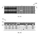
- FIG. 18is a flow diagram outlining stages in a process for making a phase change memory according to another embodiment; and FIGS. 19A-28B illustrate, in various views, stages in construction of a phase change memory according to another embodiment of the invention.
- the phase change memory elementis self-aligned only to the bit line.
- stagesare similar to earlier stages of the process outlined with reference to FIG. 1 ; and reference is made to earlier FIGs. in the discussion following.
- a common maskmay be employed for forming the first trench isolations (parallel to the bit line direction) in both the memory array region and the peripheral region.
- no silicon nitride hard maskis employed, and two different masks are employed to form second trench isolations and structures parallel to the word line direction in the memory array region.
- the bit linesare self-aligned with at least the access devices and the bottom electrodes; but the word line is not self-aligned.
- a semiconductor substrate 202is provided; typically the substrate is a single-crystal silicon substrate, but other semiconductors are contemplated.
- a device implantis carried out in a memory array region 2100 and in a peripheral region 2200 of the semiconductor substrate ( FIG. 3 , at 30 ).
- First device implantsmay be performed at this stage: to form P or N wells for access devices in the memory array region, and P or N wells for peripheral logic devices in the peripheral region.
- One or more additional implantsmay be performed at this stage including: an implant to form bit lines in the memory array region (by, for example, a N+ implant where the well is P), and implants to form elements of diode access devices or transistor access devices (by, for example, a P implant over a N+ implant, to form a N-P diode; or a P implant over a N+ implant, followed by an additional shallow N+ implant).
- one or more device implantsmay be performed at one or more subsequent stages.
- the access devices in the memory array region 2100are not shown in these FIGs. Suitable access devices include, for example, vertically-constructed devices, such as vertical diodes, vertical field effect transistors (FET), vertical bipolar junction transistors (BJT), vertical metal oxide semiconductors (MOS).
- a gate oxide layer 402is formed over the substrate surface in both the memory array region 2100 and in a peripheral region 2200 ; and in a subsequent stage a gate layer 404 is formed over the gate oxide layer 402 .
- a resultis shown at 40 in FIG. 4 .
- the gate oxide layer and the gate layerwill be patterned to form gate structures in the peripheral logic. Suitable materials for the gate layer include polysilicon, for example, and the gate layer may be formed by low pressure chemical-vapor deposition, for example.
- first trench isolationsare formed in the memory array region (trench isolations 2117 ) and in the peripheral region (trench isolations 2217 ).
- a suitable technique for forming the trenchesresults in substantially planar, approximately vertical sidewalls, and may be carried out in two or more steps.
- Suitable techniques for forming the trenchesinclude, for example, a directional etch such as, for example, an RIE.
- the RIEmay be controlled by selection of process parameters; employing lower pressure and higher substrate bias may provide better control of the shape and dimensions of the trench. Where RIE is employed, it may be followed by a cleaning process.
- a double-patterning or manifold patterning lithographic techniquemay be employed; examples of such techniques are outlined in Ping Xie et al. (2009), cited above.
- the isolation trenches in both the periphery region and the memory array regionmay be patterned using a common (shared) mask.
- Suitable materials for filling the trenchesare dielectric, and suitable dielectric materials include, for example, oxides (e.g., silicon oxides, such as SiO 2 ) and nitrides (e.g., silicon nitrides, such as SiN); low-K dielectric materials (such as a doped SiO 2 , for example) may be preferred; and materials having low thermal conductivity may be preferred.
- the dielectriccan be formed by, for example, a physical vapor deposition (PVD) process, or a chemical vapor deposition (CVD) process.
- PVDphysical vapor deposition
- CVDchemical vapor deposition
- a planarizing stepby, for example, a chemical mechanical polish, CMP may be carried out following trench filling.
- a resultis shown at 50 in FIGS. 5A , 5 B.
- second trenchesare formed in the memory array region, using a mask-and etch procedure to form patterned trenches through the SiN and through selected underlying layers.
- Preferred first critical mask materialsinclude a photoresist.
- the mask for patterning the hard mask layer (silicon nitride) in this stepis not shown in the FIGs. This constitutes a (first) critical mask step for the array; that is, the dimensions of this mask establish the array density and position.
- Suitable techniques for forming the second trenchesinclude techniques that selectively remove the unmasked SiN 602 , the unmasked gate material 504 , the unmasked gate oxide material 502 , and the unmasked semiconductor substrate 202 material; but do not remove the dielectric fill in the first trench isolations.
- the etchmay be carried out in more than one step, using etch techniques and/or etch parameters suitable for the various materials being etched.
- Suitable techniques for forming the trenchinclude, for example, a directional etch such as, for example an RIE.
- the RIEmay be controlled by selection of process parameters; employing lower pressure and higher substrate bias may provide better control of the shape and dimensions of the trench.
- a double-patterning or manifold patterning lithographic techniquemay be employed; examples of such techniques are outlined in Ping Xie et al. (2009), cited above.
- the final stage of the etchmay be timed, to establish an etch stop at the bottom of the trench.
- a memory array device implantation 1808is carried out.
- a salicide 1920is formed over the memory array, and a dielectric fill 1940 is formed.
- suitable dielectric materialsinclude, for example, oxides (e.g., silicon oxides, such as SiO 2 ) and nitrides (e.g., silicon nitrides, such as SiN); low-K dielectric materials (such as a doped SiO 2 , for example) may be preferred; and materials having low thermal conductivity may be preferred.
- the dielectriccan be formed by, for example, a physical vapor deposition (PVD) process, or a chemical vapor deposition (CVD) process.
- a planarizing step(by, for example, a chemical mechanical polish, CMP) may be carried out following trench filling.
- a resultis shown at 190 in FIGS. 19A , 19 B, 19 C.
- logic gatesare patterned (masked and etched) in the peripheral region.
- Each patterned gate(e.g., gate 2010 ) includes a gate structure 2011 stacked over a gate oxide 2013 .
- a resultis shown at 200 in FIGS. 20A , 20 B.
- Suitable materials for the logic gate maskinclude a photoresist; suitable techniques for etching include techniques that remove unmasked gate material but do not remove the isolation structures.
- a peripheral device implantationis carried out to form source and drain regions, and thereafter in the peripheral region dielectric spacers are formed adjacent the gate stacks ( 2010 ) and at exposed surfaces of the dielectric trench isolation structures ( 2012 ).
- a resultis shown at 210 in FIGS. 21A , 21 B.
- an additional array device implantis carried out, followed by formation of a salicide 2310 , 2320 over the peripheral region and the memory array region.
- a resultis shown at 230 in FIGS. 23A , 23 B.
- spacersare formed over the memory array region, to reduce the size of the exposed areas of the salicides 2310 overlying the access devices, so that only a small contact area is left exposed.
- the spacersmay be formed by, for example, depositing a layer of dielectric material over the surface and then employing an anisotropic etch to form pores to expose small areas of the underlying salicide for contact. This small contact area is, as a result of the process, aligned (“self-aligned”) with the underlying access device, and also will be aligned with the intersection of the word and bit lines, as described below.
- a word line dielectric layer 2602is formed over the planarized surface resulting from the stage 1815 , and in a stage 1817 word line trenches are formed through the word line dielectric in a second critical mask step.
- a resultis shown at 260 in FIGS. 26A , 26 B, 26 C.
- phase change material 2702is deposited into the word line trenches, in contact with the bottom electrodes, and a top electrode material 2704 is deposited over and in contact with the phase change material 2702 .
- the resulting structureis planarized. A result is shown at 270 in FIGS. 27A , 27 B.
- a dielectric coating 2802for example of borophosphosilicate glass (BPSG) is formed over the structure, and the BPSG is planarized. Then contacts are formed to couple structures in the memory array and in the periphery to the top surface of the structure.
- Contact 2816is coupled to doped region 2815 and extends to the top surface of dielectric 2802 where it can access overlying circuitry.
- Contact 2616is coupled to top electrode 2704 and extends to the top surface of dielectric 206 where it can access overlying circuitry.
- FIG. 29shows a construct having a pore structure, in which a plug of phase change material 2910 in the pore contacts the salicide beneath and contacts an overlying strip of phase change material 2902 , which is turn is overlain by an electrode 2904 .
- a contact 2916is coupled to the top electrode 2904 and extends to the top surface of dielectric 2922 where it can access overlying circuitry.
- FIG. 30shows a construct having a pore structure, in which a plug of phase change material 3010 in the pore contacts the salicide beneath and contacts an overlying electrode 3004 .
- a contact 3016is coupled to the top electrode 3004 and extends to the top surface of dielectric 3022 where it can access overlying circuitry.
Landscapes
- Semiconductor Memories (AREA)
Abstract
Description
International Business Machines Corporation, a New York corporation and Macronix International Corporation, Ltd., a Taiwan corporation, are parties to a Joint Research Agreement
This invention relates to high density memory devices based on phase change memory materials, including chalcogenide based materials, and on other programmable resistance materials, and methods for manufacturing such devices.
Phase change based memory materials, such as chalcogenide based materials and similar materials, can be caused to change phase between an amorphous state and a crystalline state by application of electrical current at levels suitable for implementation in integrated circuits. The generally amorphous state is characterized by higher electrical resistivity than the generally crystalline state, which can be readily sensed to indicate data. These properties have generated interest in using programmable resistive material to form nonvolatile memory circuits, which can be read and written with random access.
The change from the amorphous to the crystalline state is generally a lower current operation. The change from crystalline to amorphous, referred to as reset herein, is generally a higher current operation, which includes a short high current density pulse to melt or breakdown the crystalline structure, after which the phase change material cools quickly, quenching the phase change process and allowing at least a portion of the phase change material to stabilize in the amorphous state. The magnitude of the current needed for reset can be reduced by reducing the size of the phase change material element in the cell and/or the contact area between electrodes and the phase change material, such that higher current densities are achieved with small absolute current values through the phase change material element.
It is desirable to increase the density of memory cells in a memory cell array. As feature sizes are reduced, proper alignment of the memory cells with the corresponding access devices and with the word lines and bit lines presents challenges.
It is also desirable to reduce process cost in the manufacture of memory devices.
In general, a cross-point programmable memory array is disclosed in which the programmable memory cells are aligned at the access devices and at the cross-points of the bit lines and the word lines. A layer of peripheral logic devices is formed at the surface of the semiconductor substrate body and the programmable memory elements are formed over the surface of the semiconductor substrate body, so that a plane defined by the peripheral logic gates intersects the programmable memory elements. A method for making the memory array employs a damascene process in forming one or both the bit lines and the word lines; and the bit line is (or both the bit line and the word line are) self-aligned with the access devices and the programmable memory elements.
The bit lines are defined in the substrate between first isolation structures formed in trenches parallel to the bit line direction. Second isolation structures are formed in trenches parallel to the word line direction, shallower than the first isolation trenches. The first and second isolation structures extend above the semiconductor surface. The memory cell access devices are formed in the semiconductor substrate, and they are confined in one direction between the first isolation structures and in a perpendicular direction between the second isolation structures.
The word lines and the programmable memory elements are formed in word line trenches overlying the memory cell access devices, and are confined between the first isolation structures above the semiconductor substrate surface. As a result, the programmable memory elements and the access devices and the bit lines are all “self-aligned”.
In some embodiments a hard mask is used to define the second (word line) isolation trenches, and this hard mask can be left in place until the programmable memory elements and the word lines are to be formed; in these embodiments a fill can be formed over the second isolation trenches, and portions of the hard mask overlying the memory cell access devices can be selectively removed to form the word line trenches. As a result, in such embodiments the word lines, the programmable memory elements and the access devices are all “self-aligned”.
In other embodiments no hard mask is left in place, and an additional mask is used to define the word line trenches overlying the memory cell access devices. In such embodiments, the word lines and the programmable memory elements are “self-aligned” (they are formed in the word line trench by a damascene process), but the word lines and programmable memory elements are not self-aligned with the memory cell access devices.
A method for making the memory array employs a damascene process in forming one or both the bit lines and the word lines; and the bit line is (or both the bit line and the word line are) self-aligned with the access devices and the programmable memory elements.
In one aspect the invention features a programmable memory device including a semiconductor substrate body having a surface including a periphery region and a memory array region, the device including a programmable memory array in the memory array region and a layer of logic devices at the substrate surface in the periphery region, the memory array including access devices formed in the substrate body and programmable memory elements formed over the substrate surface, in which the access devices and memory elements are aligned at cross-points of bit lines and word lines, and the bit lines are self-aligned with the programmable memory elements and the access devices. In some such devices the word lines are self-aligned with the programmable memory elements and the access devices.
In another aspect the invention features a programmable memory device including a semiconductor substrate body having a surface including a periphery region and a memory array region, the device including a programmable memory array in the memory array region and a layer of logic devices at the substrate surface in the periphery region, the memory array including access devices formed in the substrate body and programmable memory elements formed over the substrate surface, in which a plane defined by peripheral logic gates intersects the programmable memory elements. In some such embodiments the access devices and memory elements are aligned at cross-points of bit lines and word lines, and the bit lines are self-aligned with the programmable memory elements and the access devices. In some such devices the word lines are self-aligned with the programmable memory elements and the access devices.
In another aspect the invention features a method for making a programmable memory array, by: providing a semiconductor substrate having a surface overlying a memory array region and a periphery region; depositing a gate oxide layer and a gate layer over the substrate surface; forming first trench isolation structures parallel to a first direction using a common mask over both the memory array region and the periphery region; removing the common mask and forming a silicon nitride layer over the gate layer and the first trench isolation structures; forming second trenches parallel to a second direction perpendicular to the first direction; forming a dielectric fill over the memory array region; patterning the periphery gate oxide layer and gate layer using a logic mask over the periphery region to form logic gates; performing a device implant in the periphery region to form source and drain regions; forming a dielectric fill over the memory array region and the periphery region and planarizing the dielectric fill; removing the silicon nitride layer and the gate layer and gate oxide layer over the memory array to form word line trenches; forming spacers on the first and second trench isolation structures in the memory array region to form pores; and forming at least one of memory cells or word lines in the word line trenches.
In another aspect the invention features a method for making a programmable memory array, by: providing a semiconductor substrate having a surface overlying a memory array region and a periphery region; depositing a gate oxide layer and a gate layer over the substrate surface; forming first trench isolation structures parallel to a first direction using a common mask over both the memory array region and the periphery region; removing the common mask and forming second trenches parallel to a second direction perpendicular to the first direction; forming a dielectric fill over the memory array region; patterning the periphery gate oxide layer and gate layer using a logic mask over the periphery region to form logic gates; performing a device implant in the periphery region to form source and drain regions; forming a dielectric fill over the memory array region and the periphery region and planarizing the dielectric fill; removing the gate layer and gate oxide layer over the memory array to form word line trenches; forming spacers on the first and second trench isolation structures in the memory array region to form pores; and forming at least one of memory cells or word lines in the word line trenches.
In some embodiments the method further includes one or more of: following forming the second trenches, forming a first memory array salicide; prior to forming the dielectric fill over the memory array region and the periphery region, forming a peripheral region salicide; prior to forming the spacers in the memory array region, forming a second memory array salicide.
In some embodiments the method further includes forming memory access device implants at one or more stages: prior to depositing the gate oxide layer over the substrate surface, following forming the second trenches, prior to forming spacers in the memory array region. In some embodiments the method further includes forming peripheral device implants in the substrate underlying the peripheral region at one or more stages: prior to depositing the gate oxide layer over the substrate surface, following forming the logic gates.
In some embodiments forming the second trenches includes forming a mask over the silicon nitride layer and, using the mask, etching to form the second trenches.
In some embodiments forming the memory cells includes depositing a programmable memory material over the second memory array salicide in the word line trenches and forming a top electrode over the programmable memory material. In some embodiments forming the memory cells includes depositing a bottom electrode material over the second memory array salicide in the word line trenches, depositing a programmable memory material over the bottom electrode material, and forming a top electrode over the programmable memory material.
In some embodiments forming memory cells over the second memory array salicide includes forming a mask over the memory array region and the periphery region, patterned to form word line trenches overlying the second memory array salicide; and depositing a programmable memory material and a top electrode in the word line trenches.
In some embodiments forming the memory cells includes depositing a programmable memory material over the second memory array salicide and forming a top electrode over the programmable memory material. In some embodiments forming the memory cells includes depositing a bottom electrode material over the second memory array salicide, depositing a programmable memory material over the bottom electrode material, and forming a top electrode over the programmable memory material.
In some embodiments the method further includes, following forming memory cells, forming a passivation layer over the memory array region and the periphery region; and forming contacts through the passivation layer to top electrodes in the memory array region and to source/drain regions in the periphery region.
In some embodiments memory cells in the memory array have an area equal to 4D2, where D is about one half the sum of the word line width and the separation distance between word lines, typically about the minimum feature size for a lithographic process used in manufacturing the memory cells.
The structure can be formed using a self-aligned process in which the word lines and memory elements are aligned with the vertical transistors without additional patterning steps. Also, the memory material is not exposed to etching chemistry during processing, leaving the memory elements damage free.
The disclosed methods provide a memory array of cells having reduced cell size, and the methods have a low processing cost, as a reduced number of masks are required.
(The various views are identified according to the following scheme: in each instance a FIG. labeled A (for example,7A) is a plan view, a FIG. labeled B is a transverse sectional view as indicated at B-B in the corresponding plan view, and a FIG. labeled C, D, or E is a transverse sectional view as indicated at C-C, D-D, or E-E, in a corresponding view. For example,FIG. 7B is a transverse sectional view as indicated at B-B inFIG. 7A ,FIG. 7C is a transverse sectional view as indicated at C-C inFIG. 7A ,FIG. 7D is a transverse sectional view as indicated at D-D inFIGS. 7A and 7B ,FIG. 7E is a transverse sectional view as indicated at E-E inFIGS. 7A and 7C .)
The invention will now be described in further detail by reference to the drawings, which illustrate alternative specific embodiments and methods. The drawings are diagrammatic, showing features of the embodiments and their relation to other features and structures, and are not made to scale. For improved clarity of presentation, in the FIGs. illustrating various embodiments, elements corresponding to elements shown in other drawings are not all particularly renumbered, although they are all readily identifiable in all the FIGs. Also for clarity of presentation certain features are not shown in the figures, where not necessary for an understanding of the invention. It is to be understood that there is no intention to limit the invention to the specifically disclosed embodiments and methods and that the invention may be practiced using other features, elements, methods and embodiments. Particular embodiments are described to illustrate the present invention, not to limit its scope, which is defined by the claims. Those of ordinary skill in the art will recognize a variety of equivalent variations on the description that follows.
The array comprises a plurality of word lines312 includingword lines bit lines array 310 is referred to as a cross-point array because the word lines312 and bit lines314 cross each other but do not physically intersect, and thememory cells 317 are located at these cross-point locations of the word lines312 and bit lines314.
Reading or writing tomemory cell 317 ofarray 310 can be achieved by applying appropriate voltage pulses to thecorresponding word line 312bandbit line 314bto induce a current through the selectedmemory cell 317. The level and duration of the voltages applied is dependent upon the operation performed, e.g., a reading operation or a programming operation.
In a read (or sense) operation of the data value stored in thememory cell 317, bias circuitry (see, e.g., biasing arrangement supply voltages,current sources 3236 ofFIG. 32 ) coupled to thecorresponding word line 312bandbit line 314bto apply bias arrangements across thememory cell 317 of suitable amplitude and duration to induce current to flow which does not result in thememory element 316 undergoing a change in resistive state. The current through thememory cell 317 is dependent upon the resistance of thememory element 316 and, thus, upon the data value stored in thememory cell 317. The data value may be determined, for example, by comparison of the current on thebit line 314bwith a suitable reference current by sense amplifiers (see, e.g., sense amplifiers/data instructures 3224 ofFIG. 32 ).
In a program operation of a data value to be stored in thememory cell 317, bias circuitry (see, e.g., biasing arrangement supply voltages,current sources 3236 ofFIG. 32 ) coupled to thecorresponding word line 312bandbit line 314bto apply bias arrangements across thememory cell 317 of suitable amplitude and duration to induce a programmable change in thememory element 316 to store the data value in thememory cell 317, the electrical resistance of thememory element 316 corresponding to the data value stored in thememory cell 317.
The bias arrangements include a first bias arrangement sufficient to forward bias thediode 318 and change the resistance state of thememory element 317 from a resistance corresponding to a first programmed state to a resistance corresponding to a second programmed state. The bias arrangements also include a second bias arrangement sufficient to forward bias thediode 318 and change the resistance state of thememory element 317 from a resistance corresponding to the second programmed state to a resistance corresponding to the first programmed state. In various embodiments the bias arrangements for unipolar operation of thememory element 317 may each comprise one or more voltage pulses, and the voltage levels and pulse times can be determined empirically for each embodiment.
Acontroller 3234 implemented in this example, using a bias arrangement state machine, controls the application of biasarrangement supply voltages 3236, such as read, program, and program verify voltages.Controller 3234 may be implemented using special-purpose logic circuitry as known in the art. In alternative embodiments,controller 3234 comprises a general-purpose processor, which may be implemented on the same integrated circuit to execute a computer program to control the operations of the device. In yet other embodiments, a combination of special-purpose logic circuitry and a general-purpose processor may be utilized for implementation ofcontroller 3234.
Embodiments of the programmable resistance material of the memory material element include phase change based memory materials, including chalcogenide based materials and other materials. Chalcogens include any of the four elements oxygen (O), sulfur (S), selenium (Se), and tellurium (Te), forming part of group VIA of the periodic table. Chalcogenides comprise compounds of a chalcogen with a more electropositive element or radical. Chalcogenide alloys comprise combinations of chalcogenides with other materials such as transition metals. A chalcogenide alloy usually contains one or more elements from group IVA of the periodic table of elements, such as germanium (Ge) and tin (Sn). Often, chalcogenide alloys include combinations including one or more of antimony (Sb), gallium (Ga), indium (In), and silver (Ag). Many phase change based memory materials have been described in technical literature, including alloys of: Ga/Sb, In/Sb, In/Se, Sb/Te, Ge/Te, Ge/Sb/Te, In/Sb/Te, Ga/Se/Te, Sn/Sb/Te, In/Sb/Ge, Ag/In/Sb/Te, Ge/Sn/Sb/Te, Ge/Sb/Se/Te and Te/Ge/Sb/S. In the family of Ge/Sb/Te alloys, a wide range of alloy compositions may be workable. The compositions can be characterized as TeaGebSb100-(a+b). One researcher has described the most useful alloys as having an average concentration of Te in the deposited materials well below 70%, typically below about 60% and ranged in general from as low as about 23% up to about 58% Te and most preferably about 48% to 58% Te. Concentrations of Ge were above about 5% and ranged from a low of about 8% to about 30% average in the material, remaining generally below 50%. Most preferably, concentrations of Ge ranged from about 8% to about 40%. The remainder of the principal constituent elements in this composition was Sb. These percentages are atomic percentages that total 100% of the atoms of the constituent elements. (Ovshinsky U.S. Pat. No. 5,687,112, columns 10-11.) Particular alloys evaluated by another researcher include Ge2Sb2Te5, GeSb2Te4and GeSb4Te7(Noboru Yamada, “Potential of Ge—Sb—Te Phase-Change Optical Disks for High-Data-Rate Recording”, SPIE v. 3109, pp. 28-37 (1997).) More generally, a transition metal such as chromium (Cr), iron (Fe), nickel (Ni), niobium (Nb), palladium (Pd), platinum (Pt) and mixtures or alloys thereof may be combined with Ge/Sb/Te to form a phase change alloy that has programmable resistance properties. Specific examples of memory materials that may be useful are given in Ovshinsky '112 at columns 11-13, which examples are hereby incorporated by reference.
Other materials, which may be termed “impurities” may be added to chalcogenides and other phase change materials in some embodiments to modify conductivity, transition temperature, melting temperature, and other properties of memory elements using the additive-modified chalcogenides. Representative impurities used as additives for chalcogenides include nitrogen, silicon, oxygen, silicon dioxide, silicon nitride, copper, silver, gold, aluminum, aluminum oxide, tantalum, tantalum oxide, tantalum nitride, titanium and titanium oxide. See, e.g., U.S. Pat. No. 6,800,504, and U.S. Patent Application Publication No. U.S. 2005/0029502.
Phase change alloys are capable of being switched between a first structural state in which the material is in a generally amorphous solid phase, and a second structural state in which the material is in a generally crystalline solid phase in its local order in the active channel region of the cell. These alloys are at least bistable. The term amorphous is used to refer to a relatively less ordered structure, more disordered than a single crystal, which has the detectable characteristics such as higher electrical resistivity than the crystalline phase. The term crystalline is used to refer to a relatively more ordered structure, more ordered than in an amorphous structure, which has detectable characteristics such as lower electrical resistivity than the amorphous phase. Typically, phase change materials may be electrically switched between different detectable states of local order across the spectrum between completely amorphous and completely crystalline states. Other material characteristics affected by the change between amorphous and crystalline phases include atomic order, free electron density and activation energy. The material may be switched either into different solid phases or into mixtures of two or more solid phases, providing a gray scale between completely amorphous and completely crystalline states. The electrical properties in the material may vary accordingly.
Phase change alloys can be changed from one phase state to another by application of electrical pulses. It has been observed that a shorter, higher amplitude pulse tends to change the phase change material to a generally amorphous state. A longer, lower amplitude pulse tends to change the phase change material to a generally crystalline state. The energy in a shorter, higher amplitude pulse is high enough to allow for bonds of the crystalline structure to be broken and short enough to prevent the atoms from realigning into a crystalline state. Appropriate profiles for pulses can be determined, without undue experimentation, specifically adapted to a particular phase change alloy. In following sections of the disclosure, the phase change material is referred to as GST, and it will be understood that other types of phase change materials can be used. A material useful for implementation of a PCRAM described herein is Ge2Sb2Te5.
Other programmable resistance memory materials may be used in other embodiments of the invention, including other materials that use different crystal phase changes to determine resistance, or other memory materials that use an electrical pulse to change the resistance state. Examples include materials for use in resistance random access memory (RRAM) such as metal-oxides including tungsten-oxide (WOx), NiO, Nb2O5, CuO2, Ta2O5, Al2O3, CoO, Fe2O3, HfO2, TiO2, SrTiO3, SrZrO3, (BaSr)TiO3. Additional examples include materials for use in magnetoresistance random access memory (MRAM) such as spin-torque-transfer (STT) MRAM, for example at least one of CoFeB, Fe, Co, Ni, Gd, Dy, CoFe, NiFe, MnAs, MnBi, MnSb, CrO2, MnOFe2O3, FeOFe2O5, NiOFe2O3, MgOFe2, EuO, and Y3Fe5O12. See, e.g., U.S. Patent Application Publication No. 2007/0176251, titled “Magnetic Memory Device and Method of Fabricating the Same”, which is incorporated by reference herein. Additional examples include solid electrolyte materials used for programmable-metallization-cell (PMC) memory, or nano-ionic memory, such as silver-doped germanium sulfide electrolytes and copper-doped germanium sulfide electrolytes. See, e.g., N. E. Gilbert et al., “A macro model of programmable metallization cell devices,” Solid-State Electronics 49 (2005) 1813-1819, which is incorporated by reference herein.
Thememory 20 includes amemory region 2100 and aperiphery region 2200 on the single-crystalline semiconductor substrate 202. Thesubstrate 202 has a substantially planar top surface. As used herein, the term “substantially planar” is intended to accommodate manufacturing tolerances during the formation of thesubstrate 202. The term “substantially planar” is also intended to accommodate manufacturing processes performed following the formation of thesubstrate 202 which may cause variations in the planarity of the top surface.
Theperiphery region 2200 includes logic devices, isolated by trench isolations, forexample trench isolation 2217. Each logic device, such aslogic device 2210, for example, has a gate structure on agate dielectric layer 2213. Thegate dielectric layer 2213 is on the top surface of thesubstrate 202. The gate structure includes alayer 2211 of doped polysilicon on thegate dielectric layer 2213, and alayer 2212 of silicide on the doped polysilicon.
Thelogic device 2210 includes dopedregions substrate 202 acting as the source and drain regions. A dielectric206 comprising one or more layers of dielectric material overlies thelogic device 2210. (The structure is presented inFIG. 2A as if the dielectric206 were transparent, so that features beneath it can be seen.)
Thememory region 2100 includes an array of access devices (not shown in these FIGs.; the position of one such device is suggested by the arrow2111), formed in the single-crystalline silicon substrate 202 and isolated by trench isolations, forexample trench isolations salicide layer 2114 overlies the access devices at the surface of thesubstrate 202 overlying the access devices. The phase change memory cells are constructed over the salicide layer at the top surface of thesubstrate 202; that is, the phase change memory cells are in the same layer (suggested by the bracket2110) as the gate structures of the peripheral logic. A variety of phase change memory cell configurations are contemplated (and some examples are described below); in the example shown in these FIGs., the memory material is a “pore structure”, including ahorizontal portion 2113 andvertical portions 2112; the vertical portions are formed in pores in a surroundingdielectric layer 204. In the example shown here, thehorizontal portion 2113 of the phase change memory material element is overlain by atop electrode 2115.Contact 2116 is coupled totop electrode 2115 and extends to the top surface ofdielectric 206 where it can access overlying circuitry.
Thebit lines 2115 are designed to have a specified bit line width and to be separated by a specified first separation distance. The word lines are designed to have a specified word line width and to be separated by a specified second separation distance. In some embodiments the summation of the specified bit line width and the specified first separation distance equals about twice a feature size D, wherein D is a nominal feature size for the lithographic process used to create the word lines and bit lines; and the summation of the specified word line width and the specified second separation distance equals about twice the feature size D. In these size constraints the memory cell has anarea 2500 equal to about 4D2.
Referring toFIG. 1 , in a stage101asemiconductor substrate 202 is provided; typically the substrate is a single-crystal silicon substrate, but other semiconductors are contemplated. In a stage103 a device implant is carried out in amemory array region 2100 and in aperipheral region 2200 of the semiconductor substrate (FIG. 3 , at30). First device implants may be performed at this stage: to form P or N wells for access devices in the memory array region, and P or N wells for peripheral logic devices in the peripheral region. One or more additional implants may be performed at this stage including: an implant to form bit lines in the memory array region (by, for example, a N+ implant where the well is P), and implants to form elements of diode access devices or transistor access devices (by, for example, a P implant over a N+ implant, to form a N-P diode; or a P implant over a N+ implant, followed by an additional shallow N+ implant). Or, one or more device implants may be performed at one or more subsequent stages.
The access devices in thememory array region 2100 are not shown in these FIGs. Suitable access devices include, for example, vertically-constructed devices, such as vertical diodes, vertical field effect transistors (FET), vertical bipolar junction transistors (BJT), vertical metal oxide semiconductors (MOS).
Subsequently, in a stage104 a gate oxide layer402 is formed over the substrate surface in both thememory array region 2100 and in aperipheral region 2200; and in a subsequent stage a gate layer404 is formed over the gate oxide layer402. A result is shown at40 inFIG. 4 . In later stages (outlined below), the gate oxide layer and the gate layer will be patterned to form gate structures in the peripheral logic. Suitable materials for the gate layer include polysilicon, for example, and the gate layer may be formed by low-pressure chemical-vapor deposition, for example.
In asubsequent stage 105 first trench isolations (parallel to the bit line direction) are formed in the memory array region (trench isolations2117) and in the peripheral region (trench isolations2217). A suitable technique for forming the trenches results in substantially planar, approximately vertical sidewalls, and may be carried out in two or more steps. Suitable techniques for forming the trench include, for example, a directional etch such as, for example, an RIE. The RIE may be controlled by selection of process parameters; employing lower pressure and higher substrate bias may provide better control of the shape and dimensions of the trench. Where RIE is employed, it may be followed by a cleaning process. A double-patterning or manifold patterning lithographic technique may be employed; examples of such techniques are outlined in Ping Xie et al. (2009) “Analysis of higher-order pitch division for sub-32 nm lithography”,Proc. of SPIE, Vol. 7274, pp. 72741Y-1 through 72741Y-8. The isolation trenches in both the periphery region and the memory array region may be patterned using a common (shared) mask.
Suitable materials for filling the trenches are dielectric, and suitable dielectric materials include, for example, oxides (e.g., silicon oxides, such as SiO2) and nitrides (e.g., silicon nitrides, such as SiN); low-K dielectric materials (such as a doped SiO2, for example) may be preferred; and materials having low thermal conductivity may be preferred. The dielectric can be formed by, for example, a physical vapor deposition (PVD) process, or a chemical vapor deposition (CVD) process. A planarizing step (by, for example, a chemical mechanical polish, CMP) may be carried out following trench filling. A result is shown at50 inFIGS. 5A ,5B.
In a subsequent stage106 asilicon nitride layer 602 is formed over the structure resulting from trench isolation. Suitable techniques for forming the silicon nitride layer include low pressure chemical vapor deposition, for example. The silicon nitride is patterned in a subsequent step, and the patterned silicon nitride serves as a hard mask for trench formation (see below). Materials other than silicon nitride, suitable for use as a hard mask, may be used to form this layer. A result is shown at60 inFIGS. 6A ,6B,6C.
In asubsequent stage 107 second trenches (parallel to the word line direction) are formed in the memory array region, using a mask-and etch procedure to form patterned trenches through the SiN and through selected underlying layers. The mask for patterning the hard mask layer (silicon nitride) in this step is not shown in the FIGs. This constitutes a (first) critical mask step for the array; that is, the dimensions of this mask establish the array density and position. Suitable techniques for forming the second trenches include techniques that selectively remove the unmaskedSiN 602, theunmasked gate material 504, the unmaskedgate oxide material 502, and theunmasked semiconductor substrate 202 material; but do not remove the dielectric fill in the first trench isolations. The etch may be carried out in more than one step, using etch techniques and/or etch parameters suitable for the various materials being etched. Suitable techniques for forming the trench include, for example, a directional etch such as, for example an RIE. The RIE may be controlled by selection of process parameters; employing lower pressure and higher substrate bias may provide better control of the shape and dimensions of the trench. A double-patterning or manifold patterning lithographic technique may be employed; examples of such techniques are outlined in Ping Xie et al. (2009), cited above. The final stage of the etch may be timed, to establish an etch stop at the bottom of the trench. A result is shown at70 inFIGS. 7A ,7B,7C.
In a subsequent stage108 a memory array device implantation may be carried out. As will be appreciated, the memory array implant must be carried out before formation of the silicon nitride mask.
In asubsequent stage 108′ optionally asalicide 820 is formed on the memory array; and adielectric fill 840 is formed. Suitable materials for filling the trenches are dielectric, and suitable dielectric materials include, for example, oxides (e.g., silicon oxides, such as SiO2) and nitrides (e.g., silicon nitrides, such as SiN); low-K dielectric materials (such as a doped SiO2, for example) may be preferred; and materials having low thermal conductivity may be preferred. The dielectric can be formed by, for example, a physical vapor deposition (PVD) process, or a chemical vapor deposition (CVD) process. A planarizing step (by, for example, a chemical mechanical polish, CMP) may be carried out following trench filling. A result is shown at80 inFIGS. 8A ,8B,8C.
The portion of theSiN layer 602 overlying the periphery region is removed, leaving in place strips920 of the SiN layer overlying the access devices. In asubsequent stage 109 logic gates (e.g.,910,910′) are patterned (masked and etched) in the peripheral region. Each patterned gate (e.g., gate910) includes agate structure 911 stacked over agate oxide 913. A result is shown at90 inFIGS. 9A ,9B. Suitable materials for the logic gate mask and suitable techniques for etching, that remove unmasked gate material but do not remove the isolation structures, are known. Thestrips 920 of SiN remaining over the memory array region protect the gate and gate oxide that overlies the memory cell devices.
In a subsequent stage110 a peripheral device implantation is carried out to form source and drain regions, and thereafter in the peripheral region dielectric spacers are formed adjacent the gate stacks (1001) and at exposed surfaces of the dielectric trench isolation structures (1002). Thereafter asalicide 1010 is formed on exposed areas of the substrate adjacent the spacers and on the exposed surfaces of the gates. A result is shown at110 inFIGS. 10A ,10B.
In asubsequent stage 111 the peripheral region is filled with a dielectric112 and the resulting structure is planarized, for example by CMP. Suitable materials for the dielectric include, for example, oxides (e.g., silicon oxides, such as SiO2) and nitrides (e.g., silicon nitrides, such as SiN); low-K dielectric materials (such as a doped SiO2, for example) may be preferred; and materials having low thermal conductivity may be preferred. The dielectric support layer can be formed by, for example, a physical vapor deposition (PVD) process, or a chemical vapor deposition (CVD) process. A result is shown at110 inFIGS. 11A ,11B.
In asubsequent stage 112 the gate oxide layer and silicon oxide layer are removed from the memory array region, by for example a selective etch. A result is shown inFIGS. 12A ,12B. In asubsequent stage 113 optionally an additional memory array implant may be carried out, optionally followed by a salicide, e.g. salicide1302. A result is shown at130 inFIGS. 13A ,13B.
In asubsequent stage 114 oxide spacers are formed on oxide sidewalls in the memory array region, with a result as shown for example at140 inFIGS. 14A ,14B,14C,14D. The oxide spacers (e.g., spacers1401) obscure much of the salicide overlying the access devices in the memory array region, so that only asmall contact area 1402 is left exposed. This small contact area is, as a result of the process, aligned (“self-aligned”) with the underlying access device, and also will be aligned with the intersection of the word and bit lines, as described below.
In asubsequent stage 115 thephase change material 1502 is deposited over the memory array region, filling in the openings over the small contact areas of exposed salicide.
In the example shown, a chalcogenide material is employed. The chalcogenide material film may be formed by vapor deposition, such as physical vapor deposition (PVD) or chemical vapor deposition (CVD), for example.
An example of a method for forming a chalcogenide material film uses a PVD-sputtering or magnetron-sputtering method with source gas(es) of Ar, N2, and/or He, etc. at the pressure in the range 1 mTorr˜100 mTorr. The deposition is usually done at room temperature. A collimator with an aspect ratio of 1˜5 can be used to improve the fill-in performance. To improve conformity with the surfaces, a DC bias of several tens of volts to several hundreds of volts may also be used. On the other hand, the combination of DC bias and the collimator can be used simultaneously.
Another example of a method for forming a chalcogenide material film uses CVD such as that disclosed in U.S. Patent Application Publication No. 2006/0172067, titled “Chemical Vapor Deposition of Chalcogenide Materials”, which is incorporated by reference herein.
Thereafter atop electrode material 1504 is deposited in contact with the phase change material, and the structure is planarized, for example by CMP. A result is shown at150 inFIGS. 15A ,15B. Suitable materials for the top electrode include conductive materials such as a metal or metal-based material or a non-metal material, such as, e.g.: copper; aluminum; titanium (Ti) and titanium-based materials such as titanium nitride (TiN), titanium ox nitride (TON); tantalum (Ta) and tantalum-based materials such as tantalum nitride (TaN); polysilicon, tungsten-based materials such as tungsten silicide (WSix); and, for a low thermal conductivity electrode, materials such as LNO (LaNiO3) and LSMO (LaSrMnO3). The top electrode layer may be formed by any of a variety of techniques suited to the particular material. Such techniques include, by way of example, sputtering and plating and CVD. The top electrode may have a thickness, for example, in a range about 200 Å to about 5000 Å, usually about 2000 Å.
A post-deposition annealing treatment in a vacuum or in an N2ambient is optionally performed to improve the crystalline state of chalcogenide material. The annealing temperature typically ranges from 100° C. to 400° C. with an anneal time of less than 30 minutes.
In a subsequent stage116 a dielectric coating, for example of borophosphosilicate glass (BPSG) is formed over the structure, and the BPSG is planarized. Then contacts are formed to couple structures in the memory array and in the periphery to the top surface of the structure.Contact 2616 is coupled to dopedregion 2615 and extends to the top surface ofdielectric 206 where it can access overlying circuitry.Contact 1616 is coupled totop electrode 1615 and extends to the top surface ofdielectric 206 where it can access overlying circuitry.
As noted above, other phase change memory array constructs are contemplated. For example, a lower electrode material may be deposited in the narrowed openings formed by the dielectric spacers over the contact layer; and a phase change material may be deposited over the lower electrode material. Such a configuration is illustrated inFIG. 17 , for example. Here thelower electrode material 1725 contacts the narrowed surface of thesalicide 1302.
Referring toFIG. 18 , stages are similar to earlier stages of the process outlined with reference toFIG. 1 ; and reference is made to earlier FIGs. in the discussion following. In this embodiment, as in the embodiment illustrated inFIG. 1 , a common mask may be employed for forming the first trench isolations (parallel to the bit line direction) in both the memory array region and the peripheral region. However, unlike the embodiment illustrated inFIG. 1 , in this embodiment no silicon nitride hard mask is employed, and two different masks are employed to form second trench isolations and structures parallel to the word line direction in the memory array region. Accordingly, in this embodiment the bit lines are self-aligned with at least the access devices and the bottom electrodes; but the word line is not self-aligned.
Particularly, in a stage1801 asemiconductor substrate 202 is provided; typically the substrate is a single-crystal silicon substrate, but other semiconductors are contemplated. In a stage1803 a device implant is carried out in amemory array region 2100 and in aperipheral region 2200 of the semiconductor substrate (FIG. 3 , at30). First device implants may be performed at this stage: to form P or N wells for access devices in the memory array region, and P or N wells for peripheral logic devices in the peripheral region. One or more additional implants may be performed at this stage including: an implant to form bit lines in the memory array region (by, for example, a N+ implant where the well is P), and implants to form elements of diode access devices or transistor access devices (by, for example, a P implant over a N+ implant, to form a N-P diode; or a P implant over a N+ implant, followed by an additional shallow N+ implant). Or, one or more device implants may be performed at one or more subsequent stages. The access devices in thememory array region 2100 are not shown in these FIGs. Suitable access devices include, for example, vertically-constructed devices, such as vertical diodes, vertical field effect transistors (FET), vertical bipolar junction transistors (BJT), vertical metal oxide semiconductors (MOS).
Subsequently, in a stage1804 a gate oxide layer402 is formed over the substrate surface in both thememory array region 2100 and in aperipheral region 2200; and in a subsequent stage a gate layer404 is formed over the gate oxide layer402. A result is shown at40 inFIG. 4 . In later stages (outlined below), the gate oxide layer and the gate layer will be patterned to form gate structures in the peripheral logic. Suitable materials for the gate layer include polysilicon, for example, and the gate layer may be formed by low pressure chemical-vapor deposition, for example.
In asubsequent stage 1805 first trench isolations (parallel to the bit line direction) are formed in the memory array region (trench isolations2117) and in the peripheral region (trench isolations2217). A suitable technique for forming the trenches results in substantially planar, approximately vertical sidewalls, and may be carried out in two or more steps. Suitable techniques for forming the trenches include, for example, a directional etch such as, for example, an RIE. The RIE may be controlled by selection of process parameters; employing lower pressure and higher substrate bias may provide better control of the shape and dimensions of the trench. Where RIE is employed, it may be followed by a cleaning process. A double-patterning or manifold patterning lithographic technique may be employed; examples of such techniques are outlined in Ping Xie et al. (2009), cited above. The isolation trenches in both the periphery region and the memory array region may be patterned using a common (shared) mask.
Suitable materials for filling the trenches are dielectric, and suitable dielectric materials include, for example, oxides (e.g., silicon oxides, such as SiO2) and nitrides (e.g., silicon nitrides, such as SiN); low-K dielectric materials (such as a doped SiO2, for example) may be preferred; and materials having low thermal conductivity may be preferred. The dielectric can be formed by, for example, a physical vapor deposition (PVD) process, or a chemical vapor deposition (CVD) process. A planarizing step (by, for example, a chemical mechanical polish, CMP) may be carried out following trench filling. A result is shown at50 inFIGS. 5A ,5B.
In asubsequent stage 1807 second trenches (parallel to the word line direction) are formed in the memory array region, using a mask-and etch procedure to form patterned trenches through the SiN and through selected underlying layers. Preferred first critical mask materials include a photoresist. The mask for patterning the hard mask layer (silicon nitride) in this step is not shown in the FIGs. This constitutes a (first) critical mask step for the array; that is, the dimensions of this mask establish the array density and position. Suitable techniques for forming the second trenches include techniques that selectively remove the unmaskedSiN 602, theunmasked gate material 504, the unmaskedgate oxide material 502, and theunmasked semiconductor substrate 202 material; but do not remove the dielectric fill in the first trench isolations. The etch may be carried out in more than one step, using etch techniques and/or etch parameters suitable for the various materials being etched. Suitable techniques for forming the trench include, for example, a directional etch such as, for example an RIE. The RIE may be controlled by selection of process parameters; employing lower pressure and higher substrate bias may provide better control of the shape and dimensions of the trench. A double-patterning or manifold patterning lithographic technique may be employed; examples of such techniques are outlined in Ping Xie et al. (2009), cited above. The final stage of the etch may be timed, to establish an etch stop at the bottom of the trench.
Thereafter a memoryarray device implantation 1808 is carried out. Optionally thereafter in aprocedure 1808′ asalicide 1920 is formed over the memory array, and adielectric fill 1940 is formed. Suitable materials for filling the trenches are dielectric, and suitable dielectric materials include, for example, oxides (e.g., silicon oxides, such as SiO2) and nitrides (e.g., silicon nitrides, such as SiN); low-K dielectric materials (such as a doped SiO2, for example) may be preferred; and materials having low thermal conductivity may be preferred. The dielectric can be formed by, for example, a physical vapor deposition (PVD) process, or a chemical vapor deposition (CVD) process. A planarizing step (by, for example, a chemical mechanical polish, CMP) may be carried out following trench filling. A result is shown at190 inFIGS. 19A ,19B,19C.
In asubsequent stage 1809 logic gates (e.g.,2010,2010′) are patterned (masked and etched) in the peripheral region. Each patterned gate (e.g., gate2010) includes agate structure 2011 stacked over agate oxide 2013. A result is shown at200 inFIGS. 20A ,20B. Suitable materials for the logic gate mask include a photoresist; suitable techniques for etching include techniques that remove unmasked gate material but do not remove the isolation structures.
In a subsequent stage1810 a peripheral device implantation is carried out to form source and drain regions, and thereafter in the peripheral region dielectric spacers are formed adjacent the gate stacks (2010) and at exposed surfaces of the dielectric trench isolation structures (2012). A result is shown at210 inFIGS. 21A ,21B.
In asubsequent stage 1812 the gate oxide layer and the silicon nitride are removed from the memory array region. A result is shown inFIGS. 22A ,22B.
In asubsequent stage 1813 optionally an additional array device implant is carried out, followed by formation of asalicide FIGS. 23A ,23B.
In asubsequent stage 1814 the peripheral region is protected by amask 2402; a result is shown at240 inFIGS. 24A ,24B.
In asubsequent stage 1815 spacers are formed over the memory array region, to reduce the size of the exposed areas of thesalicides 2310 overlying the access devices, so that only a small contact area is left exposed. A result is shown inFIGS. 25A ,25B. The spacers may be formed by, for example, depositing a layer of dielectric material over the surface and then employing an anisotropic etch to form pores to expose small areas of the underlying salicide for contact. This small contact area is, as a result of the process, aligned (“self-aligned”) with the underlying access device, and also will be aligned with the intersection of the word and bit lines, as described below.
This is followed by filling the pores or narrowed openings with abottom electrode material 2706 such as, for example, TiN and then planarizing. A result is shown at250 inFIGS. 25A ,25B.
In a subsequent stage1816 a wordline dielectric layer 2602 is formed over the planarized surface resulting from thestage 1815, and in astage 1817 word line trenches are formed through the word line dielectric in a second critical mask step. A result is shown at260 inFIGS. 26A ,26B,26C.
Thereafter aphase change material 2702 is deposited into the word line trenches, in contact with the bottom electrodes, and atop electrode material 2704 is deposited over and in contact with thephase change material 2702. The resulting structure is planarized. A result is shown at270 inFIGS. 27A ,27B.
In a subsequent stage1819 adielectric coating 2802, for example of borophosphosilicate glass (BPSG) is formed over the structure, and the BPSG is planarized. Then contacts are formed to couple structures in the memory array and in the periphery to the top surface of the structure.Contact 2816 is coupled to dopedregion 2815 and extends to the top surface of dielectric2802 where it can access overlying circuitry.Contact 2616 is coupled totop electrode 2704 and extends to the top surface ofdielectric 206 where it can access overlying circuitry.
As noted above, other phase change memory array constructs are contemplated. For example,FIG. 29 shows a construct having a pore structure, in which a plug ofphase change material 2910 in the pore contacts the salicide beneath and contacts an overlying strip ofphase change material 2902, which is turn is overlain by anelectrode 2904. Acontact 2916 is coupled to thetop electrode 2904 and extends to the top surface of dielectric2922 where it can access overlying circuitry. And, for example,FIG. 30 shows a construct having a pore structure, in which a plug ofphase change material 3010 in the pore contacts the salicide beneath and contacts anoverlying electrode 3004. Acontact 3016 is coupled to thetop electrode 3004 and extends to the top surface of dielectric3022 where it can access overlying circuitry.
Other embodiments are within the claims.
Claims (6)
1. A programmable memory device, comprising
a semiconductor substrate body having a substrate surface including a periphery region and a memory array region,
a plurality of trench isolation structures in the substrate body in both the periphery region and the memory array region, each trench isolation structure extending into the substrate body, and having a top surface that is above the substrate surface, so that inter-trench regions bounded by a plane level with the top surfaces of adjacent trench isolations structures, by sides of adjacent trench isolation structures and by the substrate surface are defined in both the periphery region and the memory array region,
a programmable memory array in the memory array region and transistors at the substrate surface in the periphery region, the transistors at the substrate surface including gates inside the inter-trench regions,
the memory array region having insulating material with pores in the inter-trench regions, the memory array comprising access devices in the substrate body and programmable memory elements over the substrate surface, wherein the access devices and memory elements are aligned at cross-points of bit lines and word lines, and at least one of a electrode element connecting the memory element with a corresponding access device, and at least a part of the memory element fill said each of said pores.
2. The programmable memory device ofclaim 1 wherein the word lines are self-aligned with the programmable memory elements and the access devices.
3. The programmable memory device ofclaim 1 wherein memory cells in the memory array have an area equal to 4D2, where D is about one half the sum of the word line width and the separation distance between word lines.
4. The programmable memory device ofclaim 1 wherein memory cells in the memory array have an area equal to 4D2, where D is about the nominal feature size for a lithographic process used in manufacturing the memory cells.
5. The programmable memory device ofclaim 1 , wherein the electrode element connecting the memory element with a corresponding access device fill said each of said pores.
6. The programmable memory device ofclaim 1 , wherein at least a portion of the memory element fill said each of said pores.
Priority Applications (3)
| Application Number | Priority Date | Filing Date | Title |
|---|---|---|---|
| US12/899,232US8395935B2 (en) | 2010-10-06 | 2010-10-06 | Cross-point self-aligned reduced cell size phase change memory |
| TW099146717ATWI426632B (en) | 2010-10-06 | 2010-12-29 | Cross-point self-aligned reduced cell size phase change memory |
| CN201110043837.0ACN102446547B (en) | 2010-10-06 | 2011-02-22 | Intersection Self-Aligned Programmable Memory Device |
Applications Claiming Priority (1)
| Application Number | Priority Date | Filing Date | Title |
|---|---|---|---|
| US12/899,232US8395935B2 (en) | 2010-10-06 | 2010-10-06 | Cross-point self-aligned reduced cell size phase change memory |
Publications (2)
| Publication Number | Publication Date |
|---|---|
| US20120087181A1 US20120087181A1 (en) | 2012-04-12 |
| US8395935B2true US8395935B2 (en) | 2013-03-12 |
Family
ID=45925028
Family Applications (1)
| Application Number | Title | Priority Date | Filing Date |
|---|---|---|---|
| US12/899,232Active2031-05-14US8395935B2 (en) | 2010-10-06 | 2010-10-06 | Cross-point self-aligned reduced cell size phase change memory |
Country Status (3)
| Country | Link |
|---|---|
| US (1) | US8395935B2 (en) |
| CN (1) | CN102446547B (en) |
| TW (1) | TWI426632B (en) |
Cited By (10)
| Publication number | Priority date | Publication date | Assignee | Title |
|---|---|---|---|---|
| US20120248529A1 (en)* | 2011-04-01 | 2012-10-04 | Jun Liu | Methods of forming vertical field-effect transistor with self-aligned contacts for memory devices with planar periphery/array and intermediate structures formed thereby |
| US9082966B2 (en) | 2013-09-26 | 2015-07-14 | Micron Technology, Inc. | Methods of forming semiconductor devices and structures with improved planarization, uniformity |
| US9306165B2 (en) | 2014-03-27 | 2016-04-05 | Micron Technology, Inc. | Replacement materials processes for forming cross point memory |
| US9454997B2 (en) | 2010-12-02 | 2016-09-27 | Micron Technology, Inc. | Array of nonvolatile memory cells having at least five memory cells per unit cell, having a plurality of the unit cells which individually comprise three elevational regions of programmable material, and/or having a continuous volume having a combination of a plurality of vertically oriented memory cells and a plurality of horizontally oriented memory cells; array of vertically stacked tiers of nonvolatile memory cells |
| US9627611B2 (en) | 2012-11-21 | 2017-04-18 | Micron Technology, Inc. | Methods for forming narrow vertical pillars and integrated circuit devices having the same |
| US9941333B2 (en) | 2016-02-22 | 2018-04-10 | Samsung Electronics Co., Ltd. | Memory device and method of manufacturing the same |
| US10297750B1 (en) | 2017-11-16 | 2019-05-21 | International Business Machines Corporation | Wraparound top electrode line for crossbar array resistive switching device |
| US10741560B2 (en) | 2017-10-26 | 2020-08-11 | International Business Machines Corporation | High resistance readout FET for cognitive device |
| US10803933B2 (en) | 2018-08-21 | 2020-10-13 | International Business Machines Corporation | Self-aligned high density and size adjustable phase change memory |
| US11751407B2 (en) | 2018-06-21 | 2023-09-05 | Macronix International Co., Ltd. | 3D memory with confined cell |
Families Citing this family (10)
| Publication number | Priority date | Publication date | Assignee | Title |
|---|---|---|---|---|
| US8603891B2 (en)* | 2012-01-20 | 2013-12-10 | Micron Technology, Inc. | Methods for forming vertical memory devices and apparatuses |
| US8946018B2 (en)* | 2012-08-21 | 2015-02-03 | Micron Technology, Inc. | Methods of forming memory arrays and semiconductor constructions |
| US8921195B2 (en) | 2012-10-26 | 2014-12-30 | International Business Machines Corporation | Isolation scheme for bipolar transistors in BiCMOS technology |
| US9601577B1 (en)* | 2015-10-08 | 2017-03-21 | Samsung Electronics Co., Ltd. | Three-dimensionally integrated circuit devices including oxidation suppression layers |
| CN109687864A (en)* | 2017-10-19 | 2019-04-26 | 成都海存艾匹科技有限公司 | Programmable gate array containing programmable computing unit |
| KR101825318B1 (en)* | 2017-01-03 | 2018-02-05 | 고려대학교 산학협력단 | Magnetic Tunnel Junction Device With Spin-Filter Structure |
| DE112017008120T5 (en)* | 2017-09-29 | 2020-11-26 | Intel Corporation | Self-aligned, embedded phase change memory cell |
| TWI735031B (en) | 2019-08-26 | 2021-08-01 | 華邦電子股份有限公司 | Resistive random access memory structure and manufacturing method thereof |
| CN112041997B (en)* | 2020-07-27 | 2024-01-12 | 长江先进存储产业创新中心有限责任公司 | New cell structure with reduced programming current and thermal cross-talk for 3D X-Point memory |
| WO2022077176A1 (en)* | 2020-10-12 | 2022-04-21 | Yangtze Advanced Memory Industrial Innovation Center Co., Ltd | A new constriction cell structure and fabrication method with reduced programming current and thermal cross talk for 3d x-point memory |
Citations (337)
| Publication number | Priority date | Publication date | Assignee | Title |
|---|---|---|---|---|
| US3271591A (en) | 1963-09-20 | 1966-09-06 | Energy Conversion Devices Inc | Symmetrical current controlling device |
| US3530441A (en) | 1969-01-15 | 1970-09-22 | Energy Conversion Devices Inc | Method and apparatus for storing and retrieving information |
| US3846767A (en) | 1973-10-24 | 1974-11-05 | Energy Conversion Devices Inc | Method and means for resetting filament-forming memory semiconductor device |
| US4452592A (en) | 1982-06-01 | 1984-06-05 | General Motors Corporation | Cyclic phase change coupling |
| US4599705A (en) | 1979-12-13 | 1986-07-08 | Energy Conversion Devices, Inc. | Programmable cell for use in programmable electronic arrays |
| US4676220A (en) | 1985-02-19 | 1987-06-30 | Pietraszek Mitchell E | Arrow rest |
| US4876220A (en) | 1986-05-16 | 1989-10-24 | Actel Corporation | Method of making programmable low impedance interconnect diode element |
| US4959812A (en) | 1987-12-28 | 1990-09-25 | Kabushiki Kaisha Toshiba | Electrically erasable programmable read-only memory with NAND cell structure |
| US5106775A (en) | 1987-12-10 | 1992-04-21 | Hitachi, Ltd. | Process for manufacturing vertical dynamic random access memories |
| US5166758A (en) | 1991-01-18 | 1992-11-24 | Energy Conversion Devices, Inc. | Electrically erasable phase change memory |
| US5166096A (en) | 1991-10-29 | 1992-11-24 | International Business Machines Corporation | Process for fabricating self-aligned contact studs for semiconductor structures |
| US5177567A (en) | 1991-07-19 | 1993-01-05 | Energy Conversion Devices, Inc. | Thin-film structure for chalcogenide electrical switching devices and process therefor |
| US5332923A (en) | 1991-08-06 | 1994-07-26 | Nec Corporation | Semiconductor memory |
| US5391901A (en) | 1992-10-30 | 1995-02-21 | Nec Corporation | Semiconductor memory with oblique folded bit-line arrangement |
| US5515488A (en) | 1994-08-30 | 1996-05-07 | Xerox Corporation | Method and apparatus for concurrent graphical visualization of a database search and its search history |
| US5534712A (en) | 1991-01-18 | 1996-07-09 | Energy Conversion Devices, Inc. | Electrically erasable memory elements characterized by reduced current and improved thermal stability |
| US5550396A (en) | 1992-01-24 | 1996-08-27 | Mitsubishi Denki Kabushiki Kaisha | Vertical field effect transistor with a trench structure |
| US5688713A (en) | 1996-08-26 | 1997-11-18 | Vanguard International Semiconductor Corporation | Method of manufacturing a DRAM cell having a double-crown capacitor using polysilicon and nitride spacers |
| US5716883A (en) | 1996-11-06 | 1998-02-10 | Vanguard International Semiconductor Corporation | Method of making increased surface area, storage node electrode, with narrow spaces between polysilicon columns |
| US5754472A (en) | 1995-12-27 | 1998-05-19 | Hyundai Electronics Industries Co., Ltd. | Flash memory device having a program path the same as a read pre-condition path |
| US5789758A (en) | 1995-06-07 | 1998-08-04 | Micron Technology, Inc. | Chalcogenide memory cell with a plurality of chalcogenide electrodes |
| US5789277A (en) | 1996-07-22 | 1998-08-04 | Micron Technology, Inc. | Method of making chalogenide memory device |
| US5814527A (en) | 1996-07-22 | 1998-09-29 | Micron Technology, Inc. | Method of making small pores defined by a disposable internal spacer for use in chalcogenide memories |
| US5831276A (en) | 1995-06-07 | 1998-11-03 | Micron Technology, Inc. | Three-dimensional container diode for use with multi-state material in a non-volatile memory cell |
| US5837564A (en) | 1995-11-01 | 1998-11-17 | Micron Technology, Inc. | Method for optimal crystallization to obtain high electrical performance from chalcogenides |
| US5869843A (en) | 1995-06-07 | 1999-02-09 | Micron Technology, Inc. | Memory array having a multi-state element and method for forming such array or cells thereof |
| US5879955A (en) | 1995-06-07 | 1999-03-09 | Micron Technology, Inc. | Method for fabricating an array of ultra-small pores for chalcogenide memory cells |
| US5902704A (en) | 1997-07-02 | 1999-05-11 | Lsi Logic Corporation | Process for forming photoresist mask over integrated circuit structures with critical dimension control |
| US5933365A (en) | 1997-06-19 | 1999-08-03 | Energy Conversion Devices, Inc. | Memory element with energy control mechanism |
| US5952671A (en) | 1997-05-09 | 1999-09-14 | Micron Technology, Inc. | Small electrode for a chalcogenide switching device and method for fabricating same |
| US5958358A (en) | 1992-07-08 | 1999-09-28 | Yeda Research And Development Co., Ltd. | Oriented polycrystalline thin films of transition metal chalcogenides |
| US5970336A (en) | 1996-08-22 | 1999-10-19 | Micron Technology, Inc. | Method of making memory cell incorporating a chalcogenide element |
| US5985698A (en) | 1996-07-22 | 1999-11-16 | Micron Technology, Inc. | Fabrication of three dimensional container diode for use with multi-state material in a non-volatile memory cell |
| US6011725A (en) | 1997-08-01 | 2000-01-04 | Saifun Semiconductors, Ltd. | Two bit non-volatile electrically erasable and programmable semiconductor memory cell utilizing asymmetrical charge trapping |
| US6031267A (en) | 1997-02-24 | 2000-02-29 | Integrated Device Technology, Inc. | Compact static RAM cell |
| US6031287A (en) | 1997-06-18 | 2000-02-29 | Micron Technology, Inc. | Contact structure and memory element incorporating the same |
| US6034882A (en) | 1998-11-16 | 2000-03-07 | Matrix Semiconductor, Inc. | Vertically stacked field programmable nonvolatile memory and method of fabrication |
| US6046951A (en) | 1998-01-23 | 2000-04-04 | Stmicroelectronics S.A. | Process for controlling the read circuit of a memory plane and corresponding memory device |
| US6066870A (en) | 1996-07-16 | 2000-05-23 | Micron Technology, Inc. | Single digit line with cell contact interconnect |
| US6075719A (en) | 1999-06-22 | 2000-06-13 | Energy Conversion Devices, Inc. | Method of programming phase-change memory element |
| US6077674A (en) | 1999-10-27 | 2000-06-20 | Agilent Technologies Inc. | Method of producing oligonucleotide arrays with features of high purity |
| US6087269A (en) | 1998-04-20 | 2000-07-11 | Advanced Micro Devices, Inc. | Method of making an interconnect using a tungsten hard mask |
| US6087674A (en) | 1996-10-28 | 2000-07-11 | Energy Conversion Devices, Inc. | Memory element with memory material comprising phase-change material and dielectric material |
| US6114713A (en) | 1997-01-28 | 2000-09-05 | Zahorik; Russell C. | Integrated circuit memory cell having a small active area and method of forming same |
| US6117720A (en) | 1995-06-07 | 2000-09-12 | Micron Technology, Inc. | Method of making an integrated circuit electrode having a reduced contact area |
| US6147395A (en) | 1996-10-02 | 2000-11-14 | Micron Technology, Inc. | Method for fabricating a small area of contact between electrodes |
| US6177317B1 (en) | 1999-04-14 | 2001-01-23 | Macronix International Co., Ltd. | Method of making nonvolatile memory devices having reduced resistance diffusion regions |
| US6214958B1 (en) | 1999-07-21 | 2001-04-10 | Arco Chemical Technology, L.P. | Process for preparing comb-branched polymers |
| WO2001045108A1 (en) | 1999-12-16 | 2001-06-21 | Ovonyx, Inc. | Programmable resistance memory arrays with reference cells |
| USRE37259E1 (en) | 1996-04-19 | 2001-07-03 | Energy Conversion Devices, Inc. | Multibit single cell memory element having tapered contact |
| US6271090B1 (en) | 2000-12-22 | 2001-08-07 | Macronix International Co., Ltd. | Method for manufacturing flash memory device with dual floating gates and two bits per cell |
| US6280684B1 (en) | 1994-12-13 | 2001-08-28 | Ricoh Company, Ltd. | Sputtering target, method of producing the target, optical recording medium fabricated by using the sputtering target, and method of fabricating the optical recording medium |
| US6291137B1 (en) | 1999-01-20 | 2001-09-18 | Advanced Micro Devices, Inc. | Sidewall formation for sidewall patterning of sub 100 nm structures |
| US6316348B1 (en) | 1999-02-05 | 2001-11-13 | Taiwan Semiconductor Manufacturing Company | High selectivity Si-rich SiON etch-stop layer |
| US6320786B1 (en) | 2000-12-22 | 2001-11-20 | Macronix International Co., Ltd. | Method of controlling multi-state NROM |
| US6326307B1 (en) | 1999-11-15 | 2001-12-04 | Appllied Materials, Inc. | Plasma pretreatment of photoresist in an oxide etch process |
| US6337266B1 (en) | 1996-07-22 | 2002-01-08 | Micron Technology, Inc. | Small electrode for chalcogenide memories |
| US6339544B1 (en) | 2000-09-29 | 2002-01-15 | Intel Corporation | Method to enhance performance of thermal resistor device |
| US20020017701A1 (en) | 1999-03-25 | 2002-02-14 | Patrick Klersy | Electrically programmable memory element with raised pore |
| US6351406B1 (en) | 1998-11-16 | 2002-02-26 | Matrix Semiconductor, Inc. | Vertically stacked field programmable nonvolatile memory and method of fabrication |
| US6372651B1 (en) | 1998-07-17 | 2002-04-16 | Advanced Micro Devices, Inc. | Method for trimming a photoresist pattern line for memory gate etching |
| US6380068B2 (en) | 2000-01-05 | 2002-04-30 | Macronix International Co., Ltd. | Method for planarizing a flash memory device |
| US20020070457A1 (en) | 2000-12-09 | 2002-06-13 | Samsung Electronics Co., Ltd. | Metal contact structure in semiconductor device and method for forming the same |
| US6420216B1 (en) | 2000-03-14 | 2002-07-16 | International Business Machines Corporation | Fuse processing using dielectric planarization pillars |
| US6420215B1 (en) | 2000-04-28 | 2002-07-16 | Matrix Semiconductor, Inc. | Three-dimensional memory array and method of fabrication |
| US6429064B1 (en) | 2000-09-29 | 2002-08-06 | Intel Corporation | Reduced contact area of sidewall conductor |
| US20020113273A1 (en) | 2001-02-22 | 2002-08-22 | Samsung Electronics Co., Ltd. | Semiconductor device having contact plug and method for manufacturing the same |
| US6440837B1 (en) | 2000-07-14 | 2002-08-27 | Micron Technology, Inc. | Method of forming a contact structure in a semiconductor device |
| US20020168852A1 (en) | 2001-05-11 | 2002-11-14 | Harshfield Steven T. | PCRAM memory cell and method of making same |
| US6483736B2 (en) | 1998-11-16 | 2002-11-19 | Matrix Semiconductor, Inc. | Vertically stacked field programmable nonvolatile memory and method of fabrication |
| US6487114B2 (en) | 2001-02-28 | 2002-11-26 | Macronix International Co., Ltd. | Method of reading two-bit memories of NROM cell |
| US6487106B1 (en) | 1999-01-12 | 2002-11-26 | Arizona Board Of Regents | Programmable microelectronic devices and method of forming and programming same |
| US20020182835A1 (en) | 2001-05-29 | 2002-12-05 | Quinn Robert M. | Method for manufacturing contacts for a Chalcogenide memory device |
| US6501111B1 (en) | 2000-06-30 | 2002-12-31 | Intel Corporation | Three-dimensional (3D) programmable device |
| US6512241B1 (en) | 2001-12-31 | 2003-01-28 | Intel Corporation | Phase change material memory device |
| US6512263B1 (en) | 2000-09-22 | 2003-01-28 | Sandisk Corporation | Non-volatile memory cell array having discontinuous source and drain diffusions contacted by continuous bit line conductors and methods of forming |
| US6511867B2 (en) | 2001-06-30 | 2003-01-28 | Ovonyx, Inc. | Utilizing atomic layer deposition for programmable device |
| US6514820B2 (en) | 1998-08-27 | 2003-02-04 | Micron Technology, Inc. | Method for forming single electron resistor memory |
| US6534781B2 (en) | 2000-12-26 | 2003-03-18 | Ovonyx, Inc. | Phase-change memory bipolar array utilizing a single shallow trench isolation for creating an individual active area region for two memory array elements and one bipolar base contact |
| US6545903B1 (en) | 2001-12-17 | 2003-04-08 | Texas Instruments Incorporated | Self-aligned resistive plugs for forming memory cell with phase change material |
| US20030072195A1 (en) | 2001-06-12 | 2003-04-17 | Thomas Mikolajick | Semiconductor memory device and fabrication method |
| US6551866B1 (en) | 1998-11-27 | 2003-04-22 | Mitsubishi Denki Kabushiki Kaisha | Method of manufacturing a semiconductor memory device |
| US6555860B2 (en) | 2000-09-29 | 2003-04-29 | Intel Corporation | Compositionally modified resistive electrode |
| US6563156B2 (en) | 2001-03-15 | 2003-05-13 | Micron Technology, Inc. | Memory elements and methods for making same |
| US6567293B1 (en) | 2000-09-29 | 2003-05-20 | Ovonyx, Inc. | Single level metal memory cell using chalcogenide cladding |
| US6566700B2 (en) | 2001-10-11 | 2003-05-20 | Ovonyx, Inc. | Carbon-containing interfacial layer for phase-change memory |
| US20030095426A1 (en) | 2001-11-20 | 2003-05-22 | Glen Hush | Complementary bit PCRAM sense amplifier and method of operation |
| US6576546B2 (en) | 1999-12-22 | 2003-06-10 | Texas Instruments Incorporated | Method of enhancing adhesion of a conductive barrier layer to an underlying conductive plug and contact for ferroelectric applications |
| US6579760B1 (en) | 2002-03-28 | 2003-06-17 | Macronix International Co., Ltd. | Self-aligned, programmable phase change memory |
| US20030116794A1 (en) | 2001-08-31 | 2003-06-26 | Lowrey Tyler A. | Elevated pore phase-change memory |
| US6586761B2 (en) | 2001-09-07 | 2003-07-01 | Intel Corporation | Phase change material memory device |
| US6589714B2 (en) | 2001-06-26 | 2003-07-08 | Ovonyx, Inc. | Method for making programmable resistance memory element using silylated photoresist |
| US6596589B2 (en) | 2001-04-30 | 2003-07-22 | Vanguard International Semiconductor Corporation | Method of manufacturing a high coupling ratio stacked gate flash memory with an HSG-SI layer |
| US6605527B2 (en) | 2001-06-30 | 2003-08-12 | Intel Corporation | Reduced area intersection between electrode and programming element |
| US6605821B1 (en) | 2002-05-10 | 2003-08-12 | Hewlett-Packard Development Company, L.P. | Phase change material electronic memory structure and method for forming |
| US6613604B2 (en) | 2001-08-02 | 2003-09-02 | Ovonyx, Inc. | Method for making small pore for use in programmable resistance memory element |
| US6617192B1 (en) | 1997-10-01 | 2003-09-09 | Ovonyx, Inc. | Electrically programmable memory element with multi-regioned contact |
| US6620715B1 (en) | 2002-03-29 | 2003-09-16 | Cypress Semiconductor Corp. | Method for forming sub-critical dimension structures in an integrated circuit |
| US6627530B2 (en) | 2000-12-22 | 2003-09-30 | Matrix Semiconductor, Inc. | Patterning three dimensional structures |
| US6639849B2 (en) | 2002-02-28 | 2003-10-28 | Fujitsu Limited | Nonvolatile semiconductor memory device programming second dynamic reference cell according to threshold value of first dynamic reference cell |
| US6674115B2 (en) | 2001-08-31 | 2004-01-06 | Intel Corporation | Multiple layer phrase-change memory |
| US6673700B2 (en) | 2001-06-30 | 2004-01-06 | Ovonyx, Inc. | Reduced area intersection between electrode and programming element |
| US6677678B2 (en) | 2000-03-14 | 2004-01-13 | International Business Machines Corporation | Damascene structure using a sacrificial conductive layer |
| US6687307B1 (en) | 2000-02-24 | 2004-02-03 | Cisco Technology, Inc | Low memory and low latency cyclic prefix addition |
| US20040026686A1 (en) | 2002-08-09 | 2004-02-12 | Macronix International Co., Ltd. | Spacer chalcogenide memory method and device |
| US20040051094A1 (en) | 2002-09-13 | 2004-03-18 | Mitsubishi Denki Kabushiki Kaisha | Non-volatile semiconductor memory device allowing shrinking of memory cell |
| WO2004025659A1 (en) | 2002-09-11 | 2004-03-25 | Ovonyx, Inc. | Programming a phase-change material memory |
| US6744088B1 (en) | 2002-12-13 | 2004-06-01 | Intel Corporation | Phase change memory device on a planar composite layer |
| US6746892B2 (en) | 2002-04-04 | 2004-06-08 | Hewlett-Packard Development Company, L.P. | Low heat loss and small contact area composite electrode for a phase change media memory device |
| US6750079B2 (en) | 1999-03-25 | 2004-06-15 | Ovonyx, Inc. | Method for making programmable resistance memory element |
| US20040113137A1 (en) | 2002-12-13 | 2004-06-17 | Lowrey Tyler A. | Memory and access device and method therefor |
| US20040114317A1 (en) | 2002-12-13 | 2004-06-17 | Chien Chiang | Forming phase change memories |
| US20040165422A1 (en) | 2003-02-24 | 2004-08-26 | Horii Hideki | Phase changeable memory devices and methods for fabricating the same |
| US6791102B2 (en) | 2002-12-13 | 2004-09-14 | Intel Corporation | Phase change memory |
| US6789277B2 (en) | 2000-06-02 | 2004-09-14 | A. Robert Spitzer | No drip bedpan |
| US6797979B2 (en) | 2000-12-21 | 2004-09-28 | Intel Corporation | Metal structure for a phase-change memory device |
| US6800563B2 (en) | 2001-10-11 | 2004-10-05 | Ovonyx, Inc. | Forming tapered lower electrode phase-change memories |
| US6800504B2 (en) | 2001-08-30 | 2004-10-05 | Micron Technology, Inc. | Integrated circuit device and fabrication using metal-doped chalcogenide materials |
| US6805563B2 (en) | 2002-09-10 | 2004-10-19 | Enplas Corporation | Socket for electrical parts |
| US6808991B1 (en) | 2003-11-19 | 2004-10-26 | Macronix International Co., Ltd. | Method for forming twin bit cell flash memory |
| US6815704B1 (en) | 2003-09-04 | 2004-11-09 | Silicon Storage Technology, Inc. | Phase change memory device employing thermally insulating voids |
| US20040248339A1 (en) | 2003-06-06 | 2004-12-09 | Lung Hsiang Lan | High density chalcogenide memory cells |
| US20040256610A1 (en) | 2003-06-23 | 2004-12-23 | Hsiang-Lan Lung | Chalcogenide memory device with multiple bits per cell |
| US20050018526A1 (en) | 2003-07-21 | 2005-01-27 | Heon Lee | Phase-change memory device and manufacturing method thereof |
| US6850432B2 (en) | 2002-08-20 | 2005-02-01 | Macronix International Co., Ltd. | Laser programmable electrically readable phase-change memory method and device |
| US20050029502A1 (en) | 2003-08-04 | 2005-02-10 | Hudgens Stephen J. | Processing phase change material to improve programming speed |
| US20050029267A1 (en) | 2003-08-05 | 2005-02-10 | Sonoco Development, Inc. | Container having a cut panel lid with a pull feature |
| US6859389B2 (en) | 2002-10-31 | 2005-02-22 | Dai Nippon Printing Co., Ltd. | Phase change-type memory element and process for producing the same |
| US6861267B2 (en) | 2001-09-17 | 2005-03-01 | Intel Corporation | Reducing shunts in memories with phase-change material |
| US6864500B2 (en) | 2002-04-10 | 2005-03-08 | Micron Technology, Inc. | Programmable conductor memory cell structure |
| US20050052904A1 (en) | 2003-09-08 | 2005-03-10 | Samsung Electronics Co., Ltd. | Initial firing method and phase change memory device for performing firing effectively |
| US6867638B2 (en) | 2002-01-10 | 2005-03-15 | Silicon Storage Technology, Inc. | High voltage generation and regulation system for digital multilevel nonvolatile memory |
| US20050062087A1 (en) | 2003-09-19 | 2005-03-24 | Yi-Chou Chen | Chalcogenide phase-change non-volatile memory, memory device and method for fabricating the same |
| US6888750B2 (en) | 2000-04-28 | 2005-05-03 | Matrix Semiconductor, Inc. | Nonvolatile memory on SOI and compound semiconductor substrates and method of fabrication |
| US6894304B2 (en) | 2001-08-27 | 2005-05-17 | Micron Technology, Inc. | Apparatus and method for dual cell common electrode PCRAM memory device |
| US6894305B2 (en) | 2003-02-24 | 2005-05-17 | Samsung Electronics Co., Ltd. | Phase-change memory devices with a self-heater structure |
| US6900517B2 (en) | 2002-04-09 | 2005-05-31 | Matsushita Electric Industrial Co., Ltd. | Non-volatile memory with phase-change recording layer |
| US6903362B2 (en) | 2001-05-09 | 2005-06-07 | Science Applications International Corporation | Phase change switches and circuits coupling to electromagnetic waves containing phase change switches |
| US20050127349A1 (en) | 2003-12-10 | 2005-06-16 | Horak David V. | Phase change tip storage cell |
| US20050127347A1 (en) | 2003-12-12 | 2005-06-16 | Suk-Hun Choi | Methods for fabricating memory devices using sacrificial layers and memory devices fabricated by same |
| US6909107B2 (en) | 2002-12-30 | 2005-06-21 | Bae Systems, Information And Electronic Systems Integration, Inc. | Method for manufacturing sidewall contacts for a chalcogenide memory device |
| US6910907B2 (en) | 2003-11-18 | 2005-06-28 | Agere Systems Inc. | Contact for use in an integrated circuit and a method of manufacture therefor |
| US20050141261A1 (en) | 2003-12-30 | 2005-06-30 | Su-Jin Ahn | Set programming methods and write driver circuits for a phase-change memory array |
| US20050145984A1 (en) | 2004-01-06 | 2005-07-07 | Yi-Chou Chen | Horizontal chalcogenide element defined by a pad for use in solid-state memories |
| US20050167656A1 (en) | 2004-01-30 | 2005-08-04 | International Business Machines Corporation | Phase-change memory cell and method of fabricating the phase-change memory cell |
| US6928022B2 (en) | 2003-11-27 | 2005-08-09 | Samsung Electronics Co., Ltd. | Write driver circuit in phase change memory device and method for applying write current |
| US6927410B2 (en) | 2003-09-04 | 2005-08-09 | Silicon Storage Technology, Inc. | Memory device with discrete layers of phase change memory material |
| US6936544B2 (en) | 2003-03-11 | 2005-08-30 | Taiwan Semiconductor Manufacturing Co., Ltd. | Method of removing metal etching residues following a metal etchback process to improve a CMP process |
| US6937507B2 (en) | 2003-12-05 | 2005-08-30 | Silicon Storage Technology, Inc. | Memory device and method of operating same |
| US20050191804A1 (en) | 2004-03-01 | 2005-09-01 | Taiwan Semiconductor Manufacturing Co., Ltd. | Method for forming a reduced active area in a phase change memory structure |
| US20050195633A1 (en) | 2004-03-05 | 2005-09-08 | Byung-Gil Choi | Method for programming phase-change memory array to set state and circuit of a phase-change memory device |
| US6943365B2 (en) | 1999-03-25 | 2005-09-13 | Ovonyx, Inc. | Electrically programmable memory element with reduced area of contact and method for making same |
| US20050201182A1 (en) | 2004-03-12 | 2005-09-15 | Kenichi Osada | Semiconductor device |
| US20050212026A1 (en) | 2004-03-26 | 2005-09-29 | Suk-Jin Chung | Trench capacitors with insulating layer collars in undercut regions and method of fabricating the same |
| US20050212024A1 (en) | 2004-03-24 | 2005-09-29 | Infineon Technologies Ag | Memory device with an active material embedded in an insulating material |
| US20050215009A1 (en) | 2004-03-19 | 2005-09-29 | Sung-Lae Cho | Methods of forming phase-change memory devices |
| US6969866B1 (en) | 1997-10-01 | 2005-11-29 | Ovonyx, Inc. | Electrically programmable memory element with improved contacts |
| US20050263829A1 (en) | 2004-05-27 | 2005-12-01 | Yoon-Jong Song | Semiconductor devices having phase change memory cells, electronic systems employing the same and methods of fabricating the same |
| US6972428B2 (en) | 2001-06-26 | 2005-12-06 | Ovonyx, Inc. | Programmable resistance memory element |
| US6972430B2 (en) | 2002-02-20 | 2005-12-06 | Stmicroelectronics S.R.L. | Sublithographic contact structure, phase change memory cell with optimized heater shape, and manufacturing method thereof |
| US6977181B1 (en) | 2004-06-17 | 2005-12-20 | Infincon Technologies Ag | MTJ stack with crystallization inhibiting layer |
| US20060006472A1 (en) | 2003-06-03 | 2006-01-12 | Hai Jiang | Phase change memory with extra-small resistors |
| US20060018156A1 (en) | 2004-07-23 | 2006-01-26 | Thomas Happ | Memory device with thermal insulating layers |
| US6992932B2 (en) | 2002-10-29 | 2006-01-31 | Saifun Semiconductors Ltd | Method circuit and system for read error detection in a non-volatile memory array |
| US20060038221A1 (en) | 2004-08-21 | 2006-02-23 | Samsung Electronics Co., Ltd. | Antiferromagnetic/paramagnetic resistive device, non-volatile memory and method for fabricating the same |
| US20060066156A1 (en) | 2004-09-30 | 2006-03-30 | Dong Qimin J | Motor rotor cooling with rotation heat pipes |
| US7023009B2 (en) | 1997-10-01 | 2006-04-04 | Ovonyx, Inc. | Electrically programmable memory element with improved contacts |
| US7023008B1 (en) | 2004-09-30 | 2006-04-04 | Infineon Technologies Ag | Resistive memory element |
| US20060073642A1 (en) | 2003-07-21 | 2006-04-06 | Macronix International Co., Ltd. | Method for manufacturing a multiple-bit-per-cell memory |
| US7038938B2 (en) | 2003-12-13 | 2006-05-02 | Hynix Semiconductor Inc. | Phase change resistor cell and nonvolatile memory device using the same |
| US20060094154A1 (en) | 2004-10-29 | 2006-05-04 | Hsiang-Lan Lung | Common word line edge contact phase-change memory |
| US20060091476A1 (en) | 2004-10-29 | 2006-05-04 | Cay-Uwe Pinnow | Sub-lithographic structures, devices including such structures, and methods for producing the same |
| US7042001B2 (en) | 2004-01-29 | 2006-05-09 | Samsung Electronics Co., Ltd. | Phase change memory devices including memory elements having variable cross-sectional areas |
| US20060110888A1 (en) | 2004-10-19 | 2006-05-25 | Byeong-Ok Cho | Phase changeable memory device and method of formation thereof |
| US20060108667A1 (en) | 2004-11-22 | 2006-05-25 | Macronix International Co., Ltd. | Method for manufacturing a small pin on integrated circuits or other devices |
| US7054183B2 (en) | 2002-10-31 | 2006-05-30 | Unity Semiconductor Corporation | Adaptive programming technique for a re-writable conductive memory device |
| US20060113520A1 (en) | 2004-12-01 | 2006-06-01 | Renesas Technology Corp. | Semiconductor integrated circuit device and method of manufacturing the same |
| US20060113521A1 (en) | 2004-11-30 | 2006-06-01 | Hsiang-Lan Lung | Chalcogenide memory having a small active region |
| US20060118913A1 (en) | 2004-12-06 | 2006-06-08 | Samsung Electronics Co., Ltd. | Phase changeable memory cells and methods of forming the same |
| US20060126395A1 (en) | 2004-12-10 | 2006-06-15 | Shih-Hung Chen | Non-volatile memory cell and operating method thereof |
| US20060124916A1 (en) | 2004-12-09 | 2006-06-15 | Macronix International Co., Ltd. | Self-aligned small contact phase-change memory method and device |
| US20060131555A1 (en) | 2004-12-22 | 2006-06-22 | Micron Technology, Inc. | Resistance variable devices with controllable channels |
| US7067837B2 (en) | 2003-04-02 | 2006-06-27 | Samsung Electronics Co., Ltd. | Phase-change memory devices |
| US7067864B2 (en) | 2001-01-30 | 2006-06-27 | Renesas Technology Corp. | SRAM having an improved capacitor |
| US20060138467A1 (en) | 2004-12-29 | 2006-06-29 | Hsiang-Lan Lung | Method of forming a small contact in phase-change memory and a memory cell produced by the method |
| US20060154185A1 (en) | 2005-01-11 | 2006-07-13 | Taiwan Semiconductor Manufacturing Co., Ltd. | Method for forming a finely patterned resist |
| US7078273B2 (en) | 2002-02-01 | 2006-07-18 | Hitachi, Ltd. | Semiconductor memory cell and method of forming same |
| US20060157680A1 (en) | 2003-05-22 | 2006-07-20 | Norikatsu Takaura | Semiconductor integrated circuit device |
| US20060163554A1 (en) | 2002-10-11 | 2006-07-27 | Koninklijke Philips Electronics N.C. | Electric device comprising phase change material |
| US20060169968A1 (en) | 2005-02-01 | 2006-08-03 | Thomas Happ | Pillar phase change memory cell |
| US20060172067A1 (en) | 2005-01-28 | 2006-08-03 | Energy Conversion Devices, Inc | Chemical vapor deposition of chalcogenide materials |
| US20060175599A1 (en) | 2005-02-10 | 2006-08-10 | Infineon Technologies North America Corp. | Phase change memory cell with high read margin at low power operation |
| US7099180B1 (en) | 2005-02-15 | 2006-08-29 | Intel Corporation | Phase change memory bits reset through a series of pulses of increasing amplitude |
| US20060192193A1 (en) | 2005-02-25 | 2006-08-31 | Samsung Electronics Co., Ltd. | Phase-change RAM and method for fabricating the same |
| US20060198183A1 (en) | 2005-03-01 | 2006-09-07 | Takayuki Kawahara | Semiconductor device |
| US20060202245A1 (en) | 2005-01-21 | 2006-09-14 | Stmicroelectronics S.R.I. | Phase-change memory device and manufacturing process thereof |
| US20060205108A1 (en) | 2001-09-19 | 2006-09-14 | Jon Maimon | Method for making tapered opening for programmable resistance memory element |
| US20060226409A1 (en) | 2005-04-06 | 2006-10-12 | International Business Machines Corporation | Structure for confining the switching current in phase memory (PCM) cells |
| US7122824B2 (en) | 2003-01-15 | 2006-10-17 | Stmicroelectronics S.R.L. | Sublithographic contact structure, in particular for a phase change memory cell, and fabrication process thereof |
| US7122281B2 (en) | 2002-02-26 | 2006-10-17 | Synopsys, Inc. | Critical dimension control using full phase and trim masks |
| US20060234138A1 (en) | 2003-09-30 | 2006-10-19 | Rodger Fehlhaber | Hard mask arrangement |
| US7126847B2 (en) | 2003-08-13 | 2006-10-24 | Samsung Electronics Co., Ltd | Method and driver for programming phase change memory cell |
| US7126149B2 (en) | 2004-01-21 | 2006-10-24 | Renesas Technology Corp. | Phase change memory and phase change recording medium |
| US20060237756A1 (en) | 2005-04-20 | 2006-10-26 | Jae-Hyun Park | Phase change memory devices and their methods of fabrication |
| US20060245236A1 (en) | 2005-05-02 | 2006-11-02 | Zaidi Shoaib H | Memory device |
| US20060261392A1 (en) | 2003-01-17 | 2006-11-23 | Samsung Electronics Co., Ltd. | Semiconductor device and method of manufacturing the same |
| US20060266993A1 (en) | 2005-05-31 | 2006-11-30 | Samsung Electronics Co., Ltd. | Phase change random access memory devices and methods of operating the same |
| US20060281216A1 (en) | 2005-06-10 | 2006-12-14 | Heon Yong Chang | Method of manufacturing a phase change RAM device utilizing reduced phase change current |
| US7151273B2 (en) | 2002-02-20 | 2006-12-19 | Micron Technology, Inc. | Silver-selenide/chalcogenide glass stack for resistance variable memory |
| US20060286709A1 (en) | 2005-06-17 | 2006-12-21 | Macronix International Co., Ltd. | Manufacturing methods for thin film fuse phase change ram |
| US20060284214A1 (en) | 2005-06-17 | 2006-12-21 | Macronix International Co., Ltd. | Thin film fuse phase change cell with thermal isolation layer and manufacturing method |
| US20060284158A1 (en) | 2005-06-17 | 2006-12-21 | Macronix International Co., Ltd. | Self-aligned, embedded phase change ram and manufacturing method |
| US20060284157A1 (en) | 2005-06-17 | 2006-12-21 | Macronix International Co., Ltd. | Thin film plate phase change RAM circuit and manufacturing method |
| US20060286743A1 (en) | 2005-06-17 | 2006-12-21 | Macronix International Co., Ltd. | Method for Manufacturing a Narrow Structure on an Integrated Circuit |
| US20060284279A1 (en) | 2005-06-17 | 2006-12-21 | Macronix International Co., Ltd. | Thin film fuse phase change RAM and manufacturing method |
| US7154774B2 (en) | 2005-03-30 | 2006-12-26 | Ovonyx, Inc. | Detecting switching of access elements of phase change memory cells |
| US20060289848A1 (en) | 2005-06-28 | 2006-12-28 | Dennison Charles H | Reducing oxidation of phase change memory electrodes |
| US20060289847A1 (en) | 2005-06-28 | 2006-12-28 | Richard Dodge | Reducing the time to program a phase change memory to the set state |
| US7158411B2 (en) | 2004-04-01 | 2007-01-02 | Macronix International Co., Ltd. | Integrated code and data flash memory |
| US20070008786A1 (en) | 2005-07-11 | 2007-01-11 | Scheuerlein Roy E | Apparatus and method for reading an array of nonvolatile memory cells including switchable resistor memory elements |
| US20070007613A1 (en) | 2005-07-08 | 2007-01-11 | Wen-Han Wang | Phase change memory with adjustable resistance ratio and fabricating method thereof |
| US20070010054A1 (en) | 2005-07-08 | 2007-01-11 | Nanochip, Inc. | Method for forming patterned media for a high density data storage device |
| US7164147B2 (en) | 2003-05-23 | 2007-01-16 | Samsung Electronics Co., Ltd. | Semiconductor memory device and method of fabricating the same |
| US7166533B2 (en) | 2005-04-08 | 2007-01-23 | Infineon Technologies, Ag | Phase change memory cell defined by a pattern shrink material process |
| US7169635B2 (en) | 2000-02-11 | 2007-01-30 | Axon Technologies Corporation | Programmable structure, an array including the structure, and methods of forming the same |
| US20070030721A1 (en) | 2001-07-25 | 2007-02-08 | Nantero, Inc. | Device selection circuitry constructed with nanotube technology |
| US20070037101A1 (en) | 2005-08-15 | 2007-02-15 | Fujitsu Limited | Manufacture method for micro structure |
| US20070040159A1 (en) | 2005-08-19 | 2007-02-22 | Wen-Han Wang | Manufacturing method and structure for improving the characteristics of phase change memory |
| US20070045606A1 (en) | 2005-08-30 | 2007-03-01 | Michele Magistretti | Shaping a phase change layer in a phase change memory cell |
| US20070051936A1 (en) | 2005-04-08 | 2007-03-08 | Stmicroelectronics S.R.I. | Phase change memory cell with tubular heater and manufacturing method thereof |
| US20070096162A1 (en) | 2005-11-02 | 2007-05-03 | Thomas Happ | Phase change memory having multilayer thermal insulation |
| US20070096248A1 (en) | 2005-10-27 | 2007-05-03 | Philipp Jan B | Phase change memory cell |
| US20070108429A1 (en) | 2005-11-14 | 2007-05-17 | Macronix International Co., Ltd. | Pipe shaped phase change memory |
| US20070111429A1 (en) | 2005-11-14 | 2007-05-17 | Macronix International Co., Ltd. | Method of manufacturing a pipe shaped phase change memory |
| US20070108077A1 (en) | 2005-11-16 | 2007-05-17 | Macronix International Co., Ltd. | Spacer Electrode Small Pin Phase Change Memory RAM and Manufacturing Method |
| US20070108431A1 (en) | 2005-11-15 | 2007-05-17 | Chen Shih H | I-shaped phase change memory cell |
| US20070108430A1 (en) | 2005-11-15 | 2007-05-17 | Macronix International Co., Ltd. | Thermally contained/insulated phase change memory device and method (combined) |
| US20070109843A1 (en) | 2005-11-15 | 2007-05-17 | Macronix International Co., Ltd. | Phase Change Memory Device and Manufacturing Method |
| US20070115794A1 (en) | 2005-11-21 | 2007-05-24 | Macronix International Co., Ltd. | Thermal isolation for an active-sidewall phase change memory cell |
| US20070117315A1 (en) | 2005-11-22 | 2007-05-24 | Macronix International Co., Ltd. | Memory cell device and manufacturing method |
| US20070121374A1 (en) | 2005-11-15 | 2007-05-31 | Macronix International Co., Ltd. | Phase Change Memory Device and Manufacturing Method |
| US20070121363A1 (en) | 2005-11-28 | 2007-05-31 | Macronix International Co., Ltd. | Phase Change Memory Cell and Manufacturing Method |
| US20070120104A1 (en) | 2005-11-29 | 2007-05-31 | Dong Ho Ahn | Phase change material and non-volatile memory device using the same |
| US20070126040A1 (en) | 2005-11-21 | 2007-06-07 | Hsiang-Lan Lung | Vacuum cell thermal isolation for a phase change memory device |
| US7229883B2 (en) | 2005-02-23 | 2007-06-12 | Taiwan Semiconductor Manufacturing Company, Ltd. | Phase change memory device and method of manufacture thereof |
| US20070131980A1 (en) | 2005-11-21 | 2007-06-14 | Lung Hsiang L | Vacuum jacket for phase change memory element |
| US20070131922A1 (en) | 2005-12-13 | 2007-06-14 | Macronix International Co., Ltd. | Thin Film Fuse Phase Change Cell with Thermal Isolation Pad and Manufacturing Method |
| US20070138458A1 (en) | 2005-06-17 | 2007-06-21 | Macronix International Co., Ltd. | Damascene Phase Change RAM and Manufacturing Method |
| US20070147105A1 (en) | 2005-11-28 | 2007-06-28 | Macronix International Co., Ltd. | Phase Change Memory Cell and Manufacturing Method |
| US7238959B2 (en) | 2004-11-01 | 2007-07-03 | Silicon Storage Technology, Inc. | Phase change memory device employing thermally insulating voids and sloped trench, and a method of making same |
| US20070154847A1 (en) | 2005-12-30 | 2007-07-05 | Macronix International Co., Ltd. | Chalcogenide layer etching method |
| US20070155172A1 (en) | 2005-12-05 | 2007-07-05 | Macronix International Co., Ltd. | Manufacturing Method for Phase Change RAM with Electrode Layer Process |
| US20070153563A1 (en) | 2006-01-03 | 2007-07-05 | Thomas Nirschl | Write circuit for resistive memory |
| US20070156949A1 (en) | 2005-12-30 | 2007-07-05 | Rudelic John C | Method and apparatus for single chip system boot |
| US20070161186A1 (en) | 2006-01-09 | 2007-07-12 | Macronix International Co., Ltd. | Programmable Resistive RAM and Manufacturing Method |
| US20070158862A1 (en) | 2005-11-21 | 2007-07-12 | Hsiang-Lan Lung | Vacuum jacketed electrode for phase change memory element |
| US20070158645A1 (en) | 2006-01-11 | 2007-07-12 | Macronix International Co., Ltd. | Self-align planerized bottom electrode phase change memory and manufacturing method |
| US20070158632A1 (en) | 2006-01-09 | 2007-07-12 | Macronix International Co., Ltd. | Method for Fabricating a Pillar-Shaped Phase Change Memory Element |
| US20070158633A1 (en) | 2005-12-27 | 2007-07-12 | Macronix International Co., Ltd. | Method for Forming Self-Aligned Thermal Isolation Cell for a Variable Resistance Memory Array |
| US20070158690A1 (en) | 2006-01-09 | 2007-07-12 | Macronix International Co., Ltd. | Programmable Resistive RAM and Manufacturing Method |
| US7248494B2 (en) | 2004-09-06 | 2007-07-24 | Samsung Electronics Co., Ltd. | Semiconductor memory device capable of compensating for leakage current |
| US20070170881A1 (en) | 2006-01-05 | 2007-07-26 | Samsung Electronics Co., Ltd. | Phase change materials, phase change random access memories having the same and methods of operating phase change random access memories |
| US20070173063A1 (en) | 2006-01-24 | 2007-07-26 | Macronix International Co., Ltd. | Self-aligned manufacturing method, and manufacturing method for thin film fuse phase change ram |
| US20070173019A1 (en) | 2006-01-09 | 2007-07-26 | Macronix International Co., Ltd. | Programmable Resistive Ram and Manufacturing Method |
| US20070176261A1 (en) | 2006-01-30 | 2007-08-02 | Macronix International Co., Ltd. | Vertical Side Wall Active Pin Structures in a Phase Change Memory and Manufacturing Methods |
| US7254059B2 (en) | 2004-10-08 | 2007-08-07 | Industrial Technology Research Institut | Multilevel phase-change memory element and operating method |
| US7262502B2 (en) | 2004-06-30 | 2007-08-28 | Hynix Semiconductor Inc. | Phase-change random access memory device and method for manufacturing the same |
| US20070201267A1 (en) | 2006-02-24 | 2007-08-30 | Thomas Happ | Sense circuit for resistive memory |
| US20070215852A1 (en) | 2006-03-15 | 2007-09-20 | Macronix International Co., Ltd. | Manufacturing method for pipe-shaped electrode phase change memory |
| US7277317B2 (en) | 2003-01-31 | 2007-10-02 | Nxp B.V. | MRAM architecture for low power consumption and high selectivity |
| US20070235811A1 (en) | 2006-04-07 | 2007-10-11 | International Business Machines Corporation | Simultaneous conditioning of a plurality of memory cells through series resistors |
| US20070249090A1 (en) | 2006-04-24 | 2007-10-25 | Philipp Jan B | Phase-change memory cell adapted to prevent over-etching or under-etching |
| US20070246699A1 (en) | 2006-04-21 | 2007-10-25 | Hsiang-Lan Lung | Phase change memory cell with vacuum spacer |
| US20070252127A1 (en) | 2006-03-30 | 2007-11-01 | Arnold John C | Phase change memory element with a peripheral connection to a thin film electrode and method of manufacture thereof |
| US7291556B2 (en) | 2003-12-12 | 2007-11-06 | Samsung Electronics Co., Ltd. | Method for forming small features in microelectronic devices using sacrificial layers |
| US20070257300A1 (en) | 2006-05-05 | 2007-11-08 | Macronix International Co., Ltd. | Structures and Methods of a Bistable Resistive Random Access Memory |
| US20070262388A1 (en) | 2006-05-09 | 2007-11-15 | Macronix International Co., Ltd. | Bridge Resistance Random Access Memory Device and Method With A Singular Contact Structure |
| US20070267618A1 (en) | 2006-05-17 | 2007-11-22 | Shoaib Zaidi | Memory device |
| US20070274121A1 (en) | 2005-06-17 | 2007-11-29 | Macronix International Co., Ltd. | Multi-level memory cell having phase change element and asymmetrical thermal boundary |
| US20070285960A1 (en) | 2006-05-24 | 2007-12-13 | Macronix International Co., Ltd. | Single-Mask Phase Change Memory Element |
| US20070298535A1 (en) | 2006-06-27 | 2007-12-27 | Macronix International Co., Ltd. | Memory Cell With Memory Material Insulation and Manufacturing Method |
| US7314776B2 (en) | 2002-12-13 | 2008-01-01 | Ovonyx, Inc. | Method to manufacture a phase change memory |
| US7317201B2 (en) | 2004-12-09 | 2008-01-08 | Infineon Technologies Ag | Method of producing a microelectronic electrode structure, and microelectronic electrode structure |
| US20080006811A1 (en) | 2006-07-10 | 2008-01-10 | Jan Boris Philipp | Integrated circuit havng a memory cell |
| US20080014676A1 (en) | 2006-07-12 | 2008-01-17 | Macronix International Co., Ltd. | Method for Making a Pillar-Type Phase Change Memory Element |
| US7323734B2 (en) | 2003-02-25 | 2008-01-29 | Samsung Electronics Co., Ltd. | Phase changeable memory cells |
| US7323708B2 (en) | 2003-07-23 | 2008-01-29 | Samsung Electronics Co., Ltd. | Phase change memory devices having phase change area in porous dielectric layer |
| US20080025089A1 (en) | 2006-07-31 | 2008-01-31 | Scheuerlein Roy E | Method for reading a multi-level passive element memory cell array |
| US20080043520A1 (en) | 2006-02-07 | 2008-02-21 | Chen Shih H | I-shaped phase change memory cell with thermal isolation |
| US7336526B2 (en) | 2005-01-05 | 2008-02-26 | Renesas Technology Corp. | Semiconductor device |
| US7351648B2 (en) | 2006-01-19 | 2008-04-01 | International Business Machines Corporation | Methods for forming uniform lithographic features |
| US20080079091A1 (en) | 2006-10-02 | 2008-04-03 | Hyun-Mog Park | NAND-type nonvolatile memory device and related method of manufacture |
| US7359231B2 (en) | 2004-06-30 | 2008-04-15 | Intel Corporation | Providing current for phase change memories |
| US20080094871A1 (en) | 2006-10-13 | 2008-04-24 | Ward Parkinson | Sequential and video access for non-volatile memory arrays |
| US7365385B2 (en) | 2004-08-30 | 2008-04-29 | Micron Technology, Inc. | DRAM layout with vertical FETs and method of formation |
| US20080101110A1 (en) | 2006-10-25 | 2008-05-01 | Thomas Happ | Combined read/write circuit for memory |
| US20080106923A1 (en) | 2006-10-24 | 2008-05-08 | Macronix International Co., Ltd. | Phase Change Memory Cells with Dual Access Devices |
| US20080137400A1 (en) | 2006-12-06 | 2008-06-12 | Macronix International Co., Ltd. | Phase Change Memory Cell with Thermal Barrier and Method for Fabricating the Same |
| US20080138930A1 (en) | 2006-12-06 | 2008-06-12 | Macronix International Co., Ltd. | Method for Making a Keyhole Opening during the Manufacture of a Memory Cell |
| US20080138931A1 (en) | 2006-12-06 | 2008-06-12 | Macronix International Co., Ltd. | Method for Making a Self-Converged Void and Bottom Electrode for Memoery Cell |
| US20080138929A1 (en) | 2006-12-06 | 2008-06-12 | Macronix International Co., Ltd. | Method for Making a Self-Converged Memory Material Element for Memory Cell |
| US7388273B2 (en) | 2005-06-14 | 2008-06-17 | International Business Machines Corporation | Reprogrammable fuse structure and method |
| US7394089B2 (en) | 2006-08-25 | 2008-07-01 | International Business Machines Corporation | Heat-shielded low power PCM-based reprogrammable EFUSE device |
| US20080165570A1 (en) | 2007-01-05 | 2008-07-10 | Macronix International Co., Ltd. | Current Compliant Sensing Architecture for Multilevel Phase Change Memory |
| US20080165569A1 (en) | 2007-01-04 | 2008-07-10 | Chieh-Fang Chen | Resistance Limited Phase Change Memory Material |
| US20080164453A1 (en) | 2007-01-07 | 2008-07-10 | Breitwisch Matthew J | Uniform critical dimension size pore for pcram application |
| US20080165572A1 (en) | 2007-01-09 | 2008-07-10 | Macronix International Co., Ltd. | Method, Apparatus and Computer Program Product for Stepped Reset Programming Process on Programmable Resistive Memory Cell |
| US7400522B2 (en) | 2003-03-18 | 2008-07-15 | Kabushiki Kaisha Toshiba | Resistance change memory device having a variable resistance element formed of a first and second composite compound for storing a cation |
| US20080179582A1 (en) | 2007-01-29 | 2008-07-31 | International Business Machines Corporation | Phase change memory element and method of making the same |
| US20080180990A1 (en) | 2007-01-31 | 2008-07-31 | Macronix International Co., Ltd. | Method to tighten set distribution for pcram |
| US20080186755A1 (en) | 2007-02-05 | 2008-08-07 | Macronix International Co., Ltd. | Memory cell device and programming methods |
| US20080191187A1 (en) | 2007-02-12 | 2008-08-14 | Macronix International Co., Ltd. | Method for manufacturing a phase change memory device with pillar bottom electrode |
| US20080192534A1 (en) | 2007-02-08 | 2008-08-14 | Macronix International Co., Ltd. | Memory element with reduced-current phase change element |
| US20080197334A1 (en) | 2007-02-21 | 2008-08-21 | Macronix International Co., Ltd. | Phase Change Memory Cell with Heater and Method for Fabricating the Same |
| US20080225489A1 (en) | 2006-10-23 | 2008-09-18 | Teledyne Licensing, Llc | Heat spreader with high heat flux and high thermal conductivity |
| US7440308B2 (en) | 2005-09-05 | 2008-10-21 | Samsung Electronics Co., Ltd. | Phase-change random access memory device and method of operating the same |
| US20080259672A1 (en) | 2007-04-17 | 2008-10-23 | Macronix International Co., Ltd. | 4f2 self align side wall active phase change memory |
| US20080265234A1 (en) | 2007-04-30 | 2008-10-30 | Breitwisch Matthew J | Method of Forming Phase Change Memory Cell With Reduced Switchable Volume |
| US20080303014A1 (en) | 2005-12-20 | 2008-12-11 | Nxp B.V. | Vertical Phase Change Memory Cell and Methods For Manufacturing Thereof |
| US20080310208A1 (en) | 2005-07-08 | 2008-12-18 | Jon Daley | Process for erasing chalcogenide variable resistance memory bits |
| US20080316794A1 (en) | 2007-06-22 | 2008-12-25 | Jan Boris Philipp | Integrated circuit having multilayer electrode |
| US20090001341A1 (en) | 2007-06-29 | 2009-01-01 | Matthew Breitwisch | Phase Change Memory with Tapered Heater |
| US20090017577A1 (en) | 2007-07-12 | 2009-01-15 | Samsung Electronics Co., Ltd. | Methods of Forming Phase Change Memory Devices Having Bottom Electrodes |
| US20090014704A1 (en) | 2007-07-11 | 2009-01-15 | International Business Machines Corporation | Current constricting phase change memory element structure |
| US20090027950A1 (en) | 2007-07-26 | 2009-01-29 | Chung Hon Lam | Block Erase for Phase Change Memory |
| US7485891B2 (en) | 2003-11-20 | 2009-02-03 | International Business Machines Corporation | Multi-bit phase change memory cell and multi-bit phase change memory including the same, method of forming a multi-bit phase change memory, and method of programming a multi-bit phase change memory |
| US7488968B2 (en) | 2005-05-05 | 2009-02-10 | Ovonyx, Inc. | Multilevel phase change memory |
| US7502252B2 (en) | 2004-10-26 | 2009-03-10 | Elpida Memory Inc. | Nonvolatile semiconductor memory device and phase change memory device |
| US20090072215A1 (en) | 2007-09-14 | 2009-03-19 | Macronix International Co., Ltd. | Phase change memory cell in via array with self-aligned, self-converged bottom electrode and method for manufacturing |
| US7514705B2 (en) | 2006-04-25 | 2009-04-07 | International Business Machines Corporation | Phase change memory cell with limited switchable volume |
| US7569844B2 (en) | 2007-04-17 | 2009-08-04 | Macronix International Co., Ltd. | Memory cell sidewall contacting side electrode |
| US20090230505A1 (en)* | 2008-03-14 | 2009-09-17 | Ovonyx, Inc. | Self-aligned memory cells and method for forming |
| US20090242865A1 (en)* | 2008-03-31 | 2009-10-01 | Macronix International Co., Ltd | Memory array with diode driver and method for fabricating the same |
| US20090268507A1 (en) | 2008-04-29 | 2009-10-29 | International Business Machines Corporation | Phase change memory device and method of manufacture |
| US20100084624A1 (en) | 2008-10-02 | 2010-04-08 | Macronix International Co., Ltd. | Dielectric mesh isolated phase change structure for phase change memory |
| US8194470B2 (en)* | 2005-12-21 | 2012-06-05 | Sandisk Technologies Inc. | Methods of forming flash device with shared word lines |
| US8198124B2 (en)* | 2010-01-05 | 2012-06-12 | Micron Technology, Inc. | Methods of self-aligned growth of chalcogenide memory access device |
- 2010
- 2010-10-06USUS12/899,232patent/US8395935B2/enactiveActive
- 2010-12-29TWTW099146717Apatent/TWI426632B/enactive
- 2011
- 2011-02-22CNCN201110043837.0Apatent/CN102446547B/enactiveActive
Patent Citations (428)
| Publication number | Priority date | Publication date | Assignee | Title |
|---|---|---|---|---|
| US3271591A (en) | 1963-09-20 | 1966-09-06 | Energy Conversion Devices Inc | Symmetrical current controlling device |
| US3530441A (en) | 1969-01-15 | 1970-09-22 | Energy Conversion Devices Inc | Method and apparatus for storing and retrieving information |
| US3846767A (en) | 1973-10-24 | 1974-11-05 | Energy Conversion Devices Inc | Method and means for resetting filament-forming memory semiconductor device |
| US4599705A (en) | 1979-12-13 | 1986-07-08 | Energy Conversion Devices, Inc. | Programmable cell for use in programmable electronic arrays |
| US4452592A (en) | 1982-06-01 | 1984-06-05 | General Motors Corporation | Cyclic phase change coupling |
| US4676220A (en) | 1985-02-19 | 1987-06-30 | Pietraszek Mitchell E | Arrow rest |
| US4876220A (en) | 1986-05-16 | 1989-10-24 | Actel Corporation | Method of making programmable low impedance interconnect diode element |
| US5106775A (en) | 1987-12-10 | 1992-04-21 | Hitachi, Ltd. | Process for manufacturing vertical dynamic random access memories |
| US4959812A (en) | 1987-12-28 | 1990-09-25 | Kabushiki Kaisha Toshiba | Electrically erasable programmable read-only memory with NAND cell structure |
| US5534712A (en) | 1991-01-18 | 1996-07-09 | Energy Conversion Devices, Inc. | Electrically erasable memory elements characterized by reduced current and improved thermal stability |
| US5166758A (en) | 1991-01-18 | 1992-11-24 | Energy Conversion Devices, Inc. | Electrically erasable phase change memory |
| US5177567A (en) | 1991-07-19 | 1993-01-05 | Energy Conversion Devices, Inc. | Thin-film structure for chalcogenide electrical switching devices and process therefor |
| US5332923A (en) | 1991-08-06 | 1994-07-26 | Nec Corporation | Semiconductor memory |
| US5166096A (en) | 1991-10-29 | 1992-11-24 | International Business Machines Corporation | Process for fabricating self-aligned contact studs for semiconductor structures |
| US5550396A (en) | 1992-01-24 | 1996-08-27 | Mitsubishi Denki Kabushiki Kaisha | Vertical field effect transistor with a trench structure |
| US5958358A (en) | 1992-07-08 | 1999-09-28 | Yeda Research And Development Co., Ltd. | Oriented polycrystalline thin films of transition metal chalcogenides |
| US5391901A (en) | 1992-10-30 | 1995-02-21 | Nec Corporation | Semiconductor memory with oblique folded bit-line arrangement |
| US5515488A (en) | 1994-08-30 | 1996-05-07 | Xerox Corporation | Method and apparatus for concurrent graphical visualization of a database search and its search history |
| US6280684B1 (en) | 1994-12-13 | 2001-08-28 | Ricoh Company, Ltd. | Sputtering target, method of producing the target, optical recording medium fabricated by using the sputtering target, and method of fabricating the optical recording medium |
| US5869843A (en) | 1995-06-07 | 1999-02-09 | Micron Technology, Inc. | Memory array having a multi-state element and method for forming such array or cells thereof |
| US5789758A (en) | 1995-06-07 | 1998-08-04 | Micron Technology, Inc. | Chalcogenide memory cell with a plurality of chalcogenide electrodes |
| US5831276A (en) | 1995-06-07 | 1998-11-03 | Micron Technology, Inc. | Three-dimensional container diode for use with multi-state material in a non-volatile memory cell |
| US20080012000A1 (en) | 1995-06-07 | 2008-01-17 | Harshfield Steven T | Method and apparatus for forming an integrated circuit electrode having a reduced contact area |
| US5879955A (en) | 1995-06-07 | 1999-03-09 | Micron Technology, Inc. | Method for fabricating an array of ultra-small pores for chalcogenide memory cells |
| US6077729A (en) | 1995-06-07 | 2000-06-20 | Micron Technology, Inc. | Memory array having a multi-state element and method for forming such array or cellis thereof |
| US5920788A (en) | 1995-06-07 | 1999-07-06 | Micron Technology, Inc. | Chalcogenide memory cell with a plurality of chalcogenide electrodes |
| US6104038A (en) | 1995-06-07 | 2000-08-15 | Micron Technology, Inc. | Method for fabricating an array of ultra-small pores for chalcogenide memory cells |
| US6420725B1 (en) | 1995-06-07 | 2002-07-16 | Micron Technology, Inc. | Method and apparatus for forming an integrated circuit electrode having a reduced contact area |
| US6117720A (en) | 1995-06-07 | 2000-09-12 | Micron Technology, Inc. | Method of making an integrated circuit electrode having a reduced contact area |
| US5837564A (en) | 1995-11-01 | 1998-11-17 | Micron Technology, Inc. | Method for optimal crystallization to obtain high electrical performance from chalcogenides |
| US5754472A (en) | 1995-12-27 | 1998-05-19 | Hyundai Electronics Industries Co., Ltd. | Flash memory device having a program path the same as a read pre-condition path |
| USRE37259E1 (en) | 1996-04-19 | 2001-07-03 | Energy Conversion Devices, Inc. | Multibit single cell memory element having tapered contact |
| US6066870A (en) | 1996-07-16 | 2000-05-23 | Micron Technology, Inc. | Single digit line with cell contact interconnect |
| US5789277A (en) | 1996-07-22 | 1998-08-04 | Micron Technology, Inc. | Method of making chalogenide memory device |
| US5985698A (en) | 1996-07-22 | 1999-11-16 | Micron Technology, Inc. | Fabrication of three dimensional container diode for use with multi-state material in a non-volatile memory cell |
| US6111264A (en) | 1996-07-22 | 2000-08-29 | Micron Technology, Inc. | Small pores defined by a disposable internal spacer for use in chalcogenide memories |
| US5814527A (en) | 1996-07-22 | 1998-09-29 | Micron Technology, Inc. | Method of making small pores defined by a disposable internal spacer for use in chalcogenide memories |
| US6337266B1 (en) | 1996-07-22 | 2002-01-08 | Micron Technology, Inc. | Small electrode for chalcogenide memories |
| US6236059B1 (en) | 1996-08-22 | 2001-05-22 | Micron Technology, Inc. | Memory cell incorporating a chalcogenide element and method of making same |
| US5998244A (en) | 1996-08-22 | 1999-12-07 | Micron Technology, Inc. | Memory cell incorporating a chalcogenide element and method of making same |
| US6153890A (en) | 1996-08-22 | 2000-11-28 | Micron Technology, Inc. | Memory cell incorporating a chalcogenide element |
| US5970336A (en) | 1996-08-22 | 1999-10-19 | Micron Technology, Inc. | Method of making memory cell incorporating a chalcogenide element |
| US5688713A (en) | 1996-08-26 | 1997-11-18 | Vanguard International Semiconductor Corporation | Method of manufacturing a DRAM cell having a double-crown capacitor using polysilicon and nitride spacers |
| US6897467B2 (en) | 1996-10-02 | 2005-05-24 | Micron Technology, Inc. | Controllable ovanic phase-change semiconductor memory device |
| US6287887B1 (en) | 1996-10-02 | 2001-09-11 | Micron Technology, Inc. | Method for fabricating a small area of contact between electrodes |
| US6423621B2 (en) | 1996-10-02 | 2002-07-23 | Micron Technology, Inc. | Controllable ovonic phase-change semiconductor memory device and methods of fabricating the same |
| US6462353B1 (en) | 1996-10-02 | 2002-10-08 | Micron Technology Inc. | Method for fabricating a small area of contact between electrodes |
| US6150253A (en) | 1996-10-02 | 2000-11-21 | Micron Technology, Inc. | Controllable ovonic phase-change semiconductor memory device and methods of fabricating the same |
| US6147395A (en) | 1996-10-02 | 2000-11-14 | Micron Technology, Inc. | Method for fabricating a small area of contact between electrodes |
| US6087674A (en) | 1996-10-28 | 2000-07-11 | Energy Conversion Devices, Inc. | Memory element with memory material comprising phase-change material and dielectric material |
| US5716883A (en) | 1996-11-06 | 1998-02-10 | Vanguard International Semiconductor Corporation | Method of making increased surface area, storage node electrode, with narrow spaces between polysilicon columns |
| US6114713A (en) | 1997-01-28 | 2000-09-05 | Zahorik; Russell C. | Integrated circuit memory cell having a small active area and method of forming same |
| US6031267A (en) | 1997-02-24 | 2000-02-29 | Integrated Device Technology, Inc. | Compact static RAM cell |
| US5952671A (en) | 1997-05-09 | 1999-09-14 | Micron Technology, Inc. | Small electrode for a chalcogenide switching device and method for fabricating same |
| US6031287A (en) | 1997-06-18 | 2000-02-29 | Micron Technology, Inc. | Contact structure and memory element incorporating the same |
| US5933365A (en) | 1997-06-19 | 1999-08-03 | Energy Conversion Devices, Inc. | Memory element with energy control mechanism |
| US5902704A (en) | 1997-07-02 | 1999-05-11 | Lsi Logic Corporation | Process for forming photoresist mask over integrated circuit structures with critical dimension control |
| US6011725A (en) | 1997-08-01 | 2000-01-04 | Saifun Semiconductors, Ltd. | Two bit non-volatile electrically erasable and programmable semiconductor memory cell utilizing asymmetrical charge trapping |
| US6969866B1 (en) | 1997-10-01 | 2005-11-29 | Ovonyx, Inc. | Electrically programmable memory element with improved contacts |
| US6617192B1 (en) | 1997-10-01 | 2003-09-09 | Ovonyx, Inc. | Electrically programmable memory element with multi-regioned contact |
| US7023009B2 (en) | 1997-10-01 | 2006-04-04 | Ovonyx, Inc. | Electrically programmable memory element with improved contacts |
| US6046951A (en) | 1998-01-23 | 2000-04-04 | Stmicroelectronics S.A. | Process for controlling the read circuit of a memory plane and corresponding memory device |
| US6087269A (en) | 1998-04-20 | 2000-07-11 | Advanced Micro Devices, Inc. | Method of making an interconnect using a tungsten hard mask |
| US6372651B1 (en) | 1998-07-17 | 2002-04-16 | Advanced Micro Devices, Inc. | Method for trimming a photoresist pattern line for memory gate etching |
| US6514820B2 (en) | 1998-08-27 | 2003-02-04 | Micron Technology, Inc. | Method for forming single electron resistor memory |
| US6034882A (en) | 1998-11-16 | 2000-03-07 | Matrix Semiconductor, Inc. | Vertically stacked field programmable nonvolatile memory and method of fabrication |
| US6483736B2 (en) | 1998-11-16 | 2002-11-19 | Matrix Semiconductor, Inc. | Vertically stacked field programmable nonvolatile memory and method of fabrication |
| US6185122B1 (en) | 1998-11-16 | 2001-02-06 | Matrix Semiconductor, Inc. | Vertically stacked field programmable nonvolatile memory and method of fabrication |
| US6351406B1 (en) | 1998-11-16 | 2002-02-26 | Matrix Semiconductor, Inc. | Vertically stacked field programmable nonvolatile memory and method of fabrication |
| US6551866B1 (en) | 1998-11-27 | 2003-04-22 | Mitsubishi Denki Kabushiki Kaisha | Method of manufacturing a semiconductor memory device |
| US6487106B1 (en) | 1999-01-12 | 2002-11-26 | Arizona Board Of Regents | Programmable microelectronic devices and method of forming and programming same |
| US6291137B1 (en) | 1999-01-20 | 2001-09-18 | Advanced Micro Devices, Inc. | Sidewall formation for sidewall patterning of sub 100 nm structures |
| US6316348B1 (en) | 1999-02-05 | 2001-11-13 | Taiwan Semiconductor Manufacturing Company | High selectivity Si-rich SiON etch-stop layer |
| US7253429B2 (en) | 1999-03-25 | 2007-08-07 | Ovonyx, Inc. | Electrically programmable memory element |
| US6750079B2 (en) | 1999-03-25 | 2004-06-15 | Ovonyx, Inc. | Method for making programmable resistance memory element |
| US20020017701A1 (en) | 1999-03-25 | 2002-02-14 | Patrick Klersy | Electrically programmable memory element with raised pore |
| US6943365B2 (en) | 1999-03-25 | 2005-09-13 | Ovonyx, Inc. | Electrically programmable memory element with reduced area of contact and method for making same |
| US6177317B1 (en) | 1999-04-14 | 2001-01-23 | Macronix International Co., Ltd. | Method of making nonvolatile memory devices having reduced resistance diffusion regions |
| US6075719A (en) | 1999-06-22 | 2000-06-13 | Energy Conversion Devices, Inc. | Method of programming phase-change memory element |
| WO2000079539A1 (en) | 1999-06-22 | 2000-12-28 | Ovonyx, Inc. | Method of programming phase-change memory element |
| US6214958B1 (en) | 1999-07-21 | 2001-04-10 | Arco Chemical Technology, L.P. | Process for preparing comb-branched polymers |
| US6077674A (en) | 1999-10-27 | 2000-06-20 | Agilent Technologies Inc. | Method of producing oligonucleotide arrays with features of high purity |
| US6326307B1 (en) | 1999-11-15 | 2001-12-04 | Appllied Materials, Inc. | Plasma pretreatment of photoresist in an oxide etch process |
| WO2001045108A1 (en) | 1999-12-16 | 2001-06-21 | Ovonyx, Inc. | Programmable resistance memory arrays with reference cells |
| US6314014B1 (en) | 1999-12-16 | 2001-11-06 | Ovonyx, Inc. | Programmable resistance memory arrays with reference cells |
| US6576546B2 (en) | 1999-12-22 | 2003-06-10 | Texas Instruments Incorporated | Method of enhancing adhesion of a conductive barrier layer to an underlying conductive plug and contact for ferroelectric applications |
| US6380068B2 (en) | 2000-01-05 | 2002-04-30 | Macronix International Co., Ltd. | Method for planarizing a flash memory device |
| US7169635B2 (en) | 2000-02-11 | 2007-01-30 | Axon Technologies Corporation | Programmable structure, an array including the structure, and methods of forming the same |
| US6687307B1 (en) | 2000-02-24 | 2004-02-03 | Cisco Technology, Inc | Low memory and low latency cyclic prefix addition |
| US6677678B2 (en) | 2000-03-14 | 2004-01-13 | International Business Machines Corporation | Damascene structure using a sacrificial conductive layer |
| US6420216B1 (en) | 2000-03-14 | 2002-07-16 | International Business Machines Corporation | Fuse processing using dielectric planarization pillars |
| US6420215B1 (en) | 2000-04-28 | 2002-07-16 | Matrix Semiconductor, Inc. | Three-dimensional memory array and method of fabrication |
| US6888750B2 (en) | 2000-04-28 | 2005-05-03 | Matrix Semiconductor, Inc. | Nonvolatile memory on SOI and compound semiconductor substrates and method of fabrication |
| US6789277B2 (en) | 2000-06-02 | 2004-09-14 | A. Robert Spitzer | No drip bedpan |
| US6501111B1 (en) | 2000-06-30 | 2002-12-31 | Intel Corporation | Three-dimensional (3D) programmable device |
| US6440837B1 (en) | 2000-07-14 | 2002-08-27 | Micron Technology, Inc. | Method of forming a contact structure in a semiconductor device |
| US6607974B2 (en) | 2000-07-14 | 2003-08-19 | Micron Technology, Inc. | Method of forming a contact structure in a semiconductor device |
| US6512263B1 (en) | 2000-09-22 | 2003-01-28 | Sandisk Corporation | Non-volatile memory cell array having discontinuous source and drain diffusions contacted by continuous bit line conductors and methods of forming |
| US6555860B2 (en) | 2000-09-29 | 2003-04-29 | Intel Corporation | Compositionally modified resistive electrode |
| US6567293B1 (en) | 2000-09-29 | 2003-05-20 | Ovonyx, Inc. | Single level metal memory cell using chalcogenide cladding |
| US6621095B2 (en) | 2000-09-29 | 2003-09-16 | Ovonyx, Inc. | Method to enhance performance of thermal resistor device |
| US6339544B1 (en) | 2000-09-29 | 2002-01-15 | Intel Corporation | Method to enhance performance of thermal resistor device |
| US6429064B1 (en) | 2000-09-29 | 2002-08-06 | Intel Corporation | Reduced contact area of sidewall conductor |
| US6597009B2 (en) | 2000-09-29 | 2003-07-22 | Intel Corporation | Reduced contact area of sidewall conductor |
| US20020070457A1 (en) | 2000-12-09 | 2002-06-13 | Samsung Electronics Co., Ltd. | Metal contact structure in semiconductor device and method for forming the same |
| US6797979B2 (en) | 2000-12-21 | 2004-09-28 | Intel Corporation | Metal structure for a phase-change memory device |
| US6627530B2 (en) | 2000-12-22 | 2003-09-30 | Matrix Semiconductor, Inc. | Patterning three dimensional structures |
| US6271090B1 (en) | 2000-12-22 | 2001-08-07 | Macronix International Co., Ltd. | Method for manufacturing flash memory device with dual floating gates and two bits per cell |
| US6320786B1 (en) | 2000-12-22 | 2001-11-20 | Macronix International Co., Ltd. | Method of controlling multi-state NROM |
| US6593176B2 (en) | 2000-12-26 | 2003-07-15 | Ovonyx, Inc. | Method for forming phase-change memory bipolar array utilizing a single shallow trench isolation for creating an individual active area region for two memory array elements and one bipolar base contact |
| US6534781B2 (en) | 2000-12-26 | 2003-03-18 | Ovonyx, Inc. | Phase-change memory bipolar array utilizing a single shallow trench isolation for creating an individual active area region for two memory array elements and one bipolar base contact |
| US7067864B2 (en) | 2001-01-30 | 2006-06-27 | Renesas Technology Corp. | SRAM having an improved capacitor |
| US20020113273A1 (en) | 2001-02-22 | 2002-08-22 | Samsung Electronics Co., Ltd. | Semiconductor device having contact plug and method for manufacturing the same |
| US6487114B2 (en) | 2001-02-28 | 2002-11-26 | Macronix International Co., Ltd. | Method of reading two-bit memories of NROM cell |
| US6563156B2 (en) | 2001-03-15 | 2003-05-13 | Micron Technology, Inc. | Memory elements and methods for making same |
| US6596589B2 (en) | 2001-04-30 | 2003-07-22 | Vanguard International Semiconductor Corporation | Method of manufacturing a high coupling ratio stacked gate flash memory with an HSG-SI layer |
| US6903362B2 (en) | 2001-05-09 | 2005-06-07 | Science Applications International Corporation | Phase change switches and circuits coupling to electromagnetic waves containing phase change switches |
| US20020168852A1 (en) | 2001-05-11 | 2002-11-14 | Harshfield Steven T. | PCRAM memory cell and method of making same |
| US20020182835A1 (en) | 2001-05-29 | 2002-12-05 | Quinn Robert M. | Method for manufacturing contacts for a Chalcogenide memory device |
| US6514788B2 (en) | 2001-05-29 | 2003-02-04 | Bae Systems Information And Electronic Systems Integration Inc. | Method for manufacturing contacts for a Chalcogenide memory device |
| US20030072195A1 (en) | 2001-06-12 | 2003-04-17 | Thomas Mikolajick | Semiconductor memory device and fabrication method |
| US6972428B2 (en) | 2001-06-26 | 2005-12-06 | Ovonyx, Inc. | Programmable resistance memory element |
| US6589714B2 (en) | 2001-06-26 | 2003-07-08 | Ovonyx, Inc. | Method for making programmable resistance memory element using silylated photoresist |
| US6605527B2 (en) | 2001-06-30 | 2003-08-12 | Intel Corporation | Reduced area intersection between electrode and programming element |
| US6511867B2 (en) | 2001-06-30 | 2003-01-28 | Ovonyx, Inc. | Utilizing atomic layer deposition for programmable device |
| US6673700B2 (en) | 2001-06-30 | 2004-01-06 | Ovonyx, Inc. | Reduced area intersection between electrode and programming element |
| US20070030721A1 (en) | 2001-07-25 | 2007-02-08 | Nantero, Inc. | Device selection circuitry constructed with nanotube technology |
| US7269052B2 (en) | 2001-07-25 | 2007-09-11 | Nantero, Inc. | Device selection circuitry constructed with nanotube technology |
| US6613604B2 (en) | 2001-08-02 | 2003-09-02 | Ovonyx, Inc. | Method for making small pore for use in programmable resistance memory element |
| US6894304B2 (en) | 2001-08-27 | 2005-05-17 | Micron Technology, Inc. | Apparatus and method for dual cell common electrode PCRAM memory device |
| US6800504B2 (en) | 2001-08-30 | 2004-10-05 | Micron Technology, Inc. | Integrated circuit device and fabrication using metal-doped chalcogenide materials |
| US6674115B2 (en) | 2001-08-31 | 2004-01-06 | Intel Corporation | Multiple layer phrase-change memory |
| US6998289B2 (en) | 2001-08-31 | 2006-02-14 | Intel Corporation | Multiple layer phase-change memory |
| US20030116794A1 (en) | 2001-08-31 | 2003-06-26 | Lowrey Tyler A. | Elevated pore phase-change memory |
| US6586761B2 (en) | 2001-09-07 | 2003-07-01 | Intel Corporation | Phase change material memory device |
| US6861267B2 (en) | 2001-09-17 | 2005-03-01 | Intel Corporation | Reducing shunts in memories with phase-change material |
| US20060205108A1 (en) | 2001-09-19 | 2006-09-14 | Jon Maimon | Method for making tapered opening for programmable resistance memory element |
| US6933516B2 (en) | 2001-10-11 | 2005-08-23 | Ovonyx, Inc. | Forming tapered lower electrode phase-change memories |
| US6566700B2 (en) | 2001-10-11 | 2003-05-20 | Ovonyx, Inc. | Carbon-containing interfacial layer for phase-change memory |
| US6800563B2 (en) | 2001-10-11 | 2004-10-05 | Ovonyx, Inc. | Forming tapered lower electrode phase-change memories |
| US6791859B2 (en) | 2001-11-20 | 2004-09-14 | Micron Technology, Inc. | Complementary bit PCRAM sense amplifier and method of operation |
| US20030095426A1 (en) | 2001-11-20 | 2003-05-22 | Glen Hush | Complementary bit PCRAM sense amplifier and method of operation |
| US6545903B1 (en) | 2001-12-17 | 2003-04-08 | Texas Instruments Incorporated | Self-aligned resistive plugs for forming memory cell with phase change material |
| US6881603B2 (en) | 2001-12-31 | 2005-04-19 | Intel Corporation | Phase change material memory device |
| US6512241B1 (en) | 2001-12-31 | 2003-01-28 | Intel Corporation | Phase change material memory device |
| US6867638B2 (en) | 2002-01-10 | 2005-03-15 | Silicon Storage Technology, Inc. | High voltage generation and regulation system for digital multilevel nonvolatile memory |
| US7078273B2 (en) | 2002-02-01 | 2006-07-18 | Hitachi, Ltd. | Semiconductor memory cell and method of forming same |
| US6972430B2 (en) | 2002-02-20 | 2005-12-06 | Stmicroelectronics S.R.L. | Sublithographic contact structure, phase change memory cell with optimized heater shape, and manufacturing method thereof |
| US7151273B2 (en) | 2002-02-20 | 2006-12-19 | Micron Technology, Inc. | Silver-selenide/chalcogenide glass stack for resistance variable memory |
| US7122281B2 (en) | 2002-02-26 | 2006-10-17 | Synopsys, Inc. | Critical dimension control using full phase and trim masks |
| US6639849B2 (en) | 2002-02-28 | 2003-10-28 | Fujitsu Limited | Nonvolatile semiconductor memory device programming second dynamic reference cell according to threshold value of first dynamic reference cell |
| US20030186481A1 (en) | 2002-03-28 | 2003-10-02 | Macronix International Co., Ltd. | Self-aligned, programmable phase change memory |
| US6579760B1 (en) | 2002-03-28 | 2003-06-17 | Macronix International Co., Ltd. | Self-aligned, programmable phase change memory |
| US6750101B2 (en) | 2002-03-28 | 2004-06-15 | Macronix International Co., Ltd. | Method of manufacturing self-aligned, programmable phase change memory |
| US6620715B1 (en) | 2002-03-29 | 2003-09-16 | Cypress Semiconductor Corp. | Method for forming sub-critical dimension structures in an integrated circuit |
| US6746892B2 (en) | 2002-04-04 | 2004-06-08 | Hewlett-Packard Development Company, L.P. | Low heat loss and small contact area composite electrode for a phase change media memory device |
| US6900517B2 (en) | 2002-04-09 | 2005-05-31 | Matsushita Electric Industrial Co., Ltd. | Non-volatile memory with phase-change recording layer |
| US6864500B2 (en) | 2002-04-10 | 2005-03-08 | Micron Technology, Inc. | Programmable conductor memory cell structure |
| US7132675B2 (en) | 2002-04-10 | 2006-11-07 | Micron Technology, Inc. | Programmable conductor memory cell structure and method therefor |
| US6605821B1 (en) | 2002-05-10 | 2003-08-12 | Hewlett-Packard Development Company, L.P. | Phase change material electronic memory structure and method for forming |
| US7033856B2 (en) | 2002-08-09 | 2006-04-25 | Macronix International Co. Ltd | Spacer chalcogenide memory method |
| US20050093022A1 (en) | 2002-08-09 | 2005-05-05 | Macronix International Co., Ltd. | Spacer chalcogenide memory device |
| US20040026686A1 (en) | 2002-08-09 | 2004-02-12 | Macronix International Co., Ltd. | Spacer chalcogenide memory method and device |
| US6864503B2 (en) | 2002-08-09 | 2005-03-08 | Macronix International Co., Ltd. | Spacer chalcogenide memory method and device |
| US7385235B2 (en) | 2002-08-09 | 2008-06-10 | Macronix International Co., Ltd. | Spacer chalcogenide memory device |
| US6830952B2 (en) | 2002-08-09 | 2004-12-14 | Macronix International Co., Ltd. | Spacer chalcogenide memory method and device |
| US6850432B2 (en) | 2002-08-20 | 2005-02-01 | Macronix International Co., Ltd. | Laser programmable electrically readable phase-change memory method and device |
| US6805563B2 (en) | 2002-09-10 | 2004-10-19 | Enplas Corporation | Socket for electrical parts |
| WO2004025659A1 (en) | 2002-09-11 | 2004-03-25 | Ovonyx, Inc. | Programming a phase-change material memory |
| US20040051094A1 (en) | 2002-09-13 | 2004-03-18 | Mitsubishi Denki Kabushiki Kaisha | Non-volatile semiconductor memory device allowing shrinking of memory cell |
| US7208751B2 (en) | 2002-09-13 | 2007-04-24 | Renesas Technology Corp. | Non-volatile semiconductor memory device allowing shrinking of memory cell |
| US20060163554A1 (en) | 2002-10-11 | 2006-07-27 | Koninklijke Philips Electronics N.C. | Electric device comprising phase change material |
| US6992932B2 (en) | 2002-10-29 | 2006-01-31 | Saifun Semiconductors Ltd | Method circuit and system for read error detection in a non-volatile memory array |
| US7054183B2 (en) | 2002-10-31 | 2006-05-30 | Unity Semiconductor Corporation | Adaptive programming technique for a re-writable conductive memory device |
| US6859389B2 (en) | 2002-10-31 | 2005-02-22 | Dai Nippon Printing Co., Ltd. | Phase change-type memory element and process for producing the same |
| US6791102B2 (en) | 2002-12-13 | 2004-09-14 | Intel Corporation | Phase change memory |
| US20040114317A1 (en) | 2002-12-13 | 2004-06-17 | Chien Chiang | Forming phase change memories |
| US7314776B2 (en) | 2002-12-13 | 2008-01-01 | Ovonyx, Inc. | Method to manufacture a phase change memory |
| US20040113137A1 (en) | 2002-12-13 | 2004-06-17 | Lowrey Tyler A. | Memory and access device and method therefor |
| US6744088B1 (en) | 2002-12-13 | 2004-06-01 | Intel Corporation | Phase change memory device on a planar composite layer |
| US6909107B2 (en) | 2002-12-30 | 2005-06-21 | Bae Systems, Information And Electronic Systems Integration, Inc. | Method for manufacturing sidewall contacts for a chalcogenide memory device |
| US7122824B2 (en) | 2003-01-15 | 2006-10-17 | Stmicroelectronics S.R.L. | Sublithographic contact structure, in particular for a phase change memory cell, and fabrication process thereof |
| US20060261392A1 (en) | 2003-01-17 | 2006-11-23 | Samsung Electronics Co., Ltd. | Semiconductor device and method of manufacturing the same |
| US7277317B2 (en) | 2003-01-31 | 2007-10-02 | Nxp B.V. | MRAM architecture for low power consumption and high selectivity |
| US6894305B2 (en) | 2003-02-24 | 2005-05-17 | Samsung Electronics Co., Ltd. | Phase-change memory devices with a self-heater structure |
| US7115927B2 (en) | 2003-02-24 | 2006-10-03 | Samsung Electronics Co., Ltd. | Phase changeable memory devices |
| US20040165422A1 (en) | 2003-02-24 | 2004-08-26 | Horii Hideki | Phase changeable memory devices and methods for fabricating the same |
| US7323734B2 (en) | 2003-02-25 | 2008-01-29 | Samsung Electronics Co., Ltd. | Phase changeable memory cells |
| US6936544B2 (en) | 2003-03-11 | 2005-08-30 | Taiwan Semiconductor Manufacturing Co., Ltd. | Method of removing metal etching residues following a metal etchback process to improve a CMP process |
| US7400522B2 (en) | 2003-03-18 | 2008-07-15 | Kabushiki Kaisha Toshiba | Resistance change memory device having a variable resistance element formed of a first and second composite compound for storing a cation |
| US20060211165A1 (en) | 2003-04-02 | 2006-09-21 | Young-Nam Hwang | Methods for forming phase-change memory devices |
| US7067837B2 (en) | 2003-04-02 | 2006-06-27 | Samsung Electronics Co., Ltd. | Phase-change memory devices |
| US20060157680A1 (en) | 2003-05-22 | 2006-07-20 | Norikatsu Takaura | Semiconductor integrated circuit device |
| US7164147B2 (en) | 2003-05-23 | 2007-01-16 | Samsung Electronics Co., Ltd. | Semiconductor memory device and method of fabricating the same |
| US20060006472A1 (en) | 2003-06-03 | 2006-01-12 | Hai Jiang | Phase change memory with extra-small resistors |
| US20040248339A1 (en) | 2003-06-06 | 2004-12-09 | Lung Hsiang Lan | High density chalcogenide memory cells |
| US7067865B2 (en) | 2003-06-06 | 2006-06-27 | Macronix International Co., Ltd. | High density chalcogenide memory cells |
| US20040256610A1 (en) | 2003-06-23 | 2004-12-23 | Hsiang-Lan Lung | Chalcogenide memory device with multiple bits per cell |
| US6838692B1 (en) | 2003-06-23 | 2005-01-04 | Macronix International Co., Ltd. | Chalcogenide memory device with multiple bits per cell |
| US20060073642A1 (en) | 2003-07-21 | 2006-04-06 | Macronix International Co., Ltd. | Method for manufacturing a multiple-bit-per-cell memory |
| US20050018526A1 (en) | 2003-07-21 | 2005-01-27 | Heon Lee | Phase-change memory device and manufacturing method thereof |
| US7323708B2 (en) | 2003-07-23 | 2008-01-29 | Samsung Electronics Co., Ltd. | Phase change memory devices having phase change area in porous dielectric layer |
| US20050029502A1 (en) | 2003-08-04 | 2005-02-10 | Hudgens Stephen J. | Processing phase change material to improve programming speed |
| US20050029267A1 (en) | 2003-08-05 | 2005-02-10 | Sonoco Development, Inc. | Container having a cut panel lid with a pull feature |
| US7126847B2 (en) | 2003-08-13 | 2006-10-24 | Samsung Electronics Co., Ltd | Method and driver for programming phase change memory cell |
| US6927410B2 (en) | 2003-09-04 | 2005-08-09 | Silicon Storage Technology, Inc. | Memory device with discrete layers of phase change memory material |
| US6815704B1 (en) | 2003-09-04 | 2004-11-09 | Silicon Storage Technology, Inc. | Phase change memory device employing thermally insulating voids |
| US20060250885A1 (en) | 2003-09-08 | 2006-11-09 | Samsung Electronics, Co., Ltd. | Initial firing method and phase change memory device for performing firing effectively |
| US20050052904A1 (en) | 2003-09-08 | 2005-03-10 | Samsung Electronics Co., Ltd. | Initial firing method and phase change memory device for performing firing effectively |
| US20050062087A1 (en) | 2003-09-19 | 2005-03-24 | Yi-Chou Chen | Chalcogenide phase-change non-volatile memory, memory device and method for fabricating the same |
| US20060234138A1 (en) | 2003-09-30 | 2006-10-19 | Rodger Fehlhaber | Hard mask arrangement |
| US6910907B2 (en) | 2003-11-18 | 2005-06-28 | Agere Systems Inc. | Contact for use in an integrated circuit and a method of manufacture therefor |
| US6808991B1 (en) | 2003-11-19 | 2004-10-26 | Macronix International Co., Ltd. | Method for forming twin bit cell flash memory |
| US7485891B2 (en) | 2003-11-20 | 2009-02-03 | International Business Machines Corporation | Multi-bit phase change memory cell and multi-bit phase change memory including the same, method of forming a multi-bit phase change memory, and method of programming a multi-bit phase change memory |
| US6928022B2 (en) | 2003-11-27 | 2005-08-09 | Samsung Electronics Co., Ltd. | Write driver circuit in phase change memory device and method for applying write current |
| US6937507B2 (en) | 2003-12-05 | 2005-08-30 | Silicon Storage Technology, Inc. | Memory device and method of operating same |
| US20050127349A1 (en) | 2003-12-10 | 2005-06-16 | Horak David V. | Phase change tip storage cell |
| US7291556B2 (en) | 2003-12-12 | 2007-11-06 | Samsung Electronics Co., Ltd. | Method for forming small features in microelectronic devices using sacrificial layers |
| US20050127347A1 (en) | 2003-12-12 | 2005-06-16 | Suk-Hun Choi | Methods for fabricating memory devices using sacrificial layers and memory devices fabricated by same |
| US7038938B2 (en) | 2003-12-13 | 2006-05-02 | Hynix Semiconductor Inc. | Phase change resistor cell and nonvolatile memory device using the same |
| US20050141261A1 (en) | 2003-12-30 | 2005-06-30 | Su-Jin Ahn | Set programming methods and write driver circuits for a phase-change memory array |
| US7038230B2 (en) | 2004-01-06 | 2006-05-02 | Macronix Internation Co., Ltd. | Horizontal chalcogenide element defined by a pad for use in solid-state memories |
| US20050145984A1 (en) | 2004-01-06 | 2005-07-07 | Yi-Chou Chen | Horizontal chalcogenide element defined by a pad for use in solid-state memories |
| US20060157681A1 (en) | 2004-01-06 | 2006-07-20 | Yi-Chou Chen | Horizontal chalcogenide element defined by a pad for use in solid-state memories |
| US7683360B2 (en) | 2004-01-06 | 2010-03-23 | Macronix International Co., Ltd. | Horizontal chalcogenide element defined by a pad for use in solid-state memories |
| US7126149B2 (en) | 2004-01-21 | 2006-10-24 | Renesas Technology Corp. | Phase change memory and phase change recording medium |
| US7042001B2 (en) | 2004-01-29 | 2006-05-09 | Samsung Electronics Co., Ltd. | Phase change memory devices including memory elements having variable cross-sectional areas |
| US6936840B2 (en) | 2004-01-30 | 2005-08-30 | International Business Machines Corporation | Phase-change memory cell and method of fabricating the phase-change memory cell |
| US20050167656A1 (en) | 2004-01-30 | 2005-08-04 | International Business Machines Corporation | Phase-change memory cell and method of fabricating the phase-change memory cell |
| US20050191804A1 (en) | 2004-03-01 | 2005-09-01 | Taiwan Semiconductor Manufacturing Co., Ltd. | Method for forming a reduced active area in a phase change memory structure |
| US20050195633A1 (en) | 2004-03-05 | 2005-09-08 | Byung-Gil Choi | Method for programming phase-change memory array to set state and circuit of a phase-change memory device |
| US7379328B2 (en) | 2004-03-12 | 2008-05-27 | Hitachi, Ltd. | Semiconductor device |
| US20050201182A1 (en) | 2004-03-12 | 2005-09-15 | Kenichi Osada | Semiconductor device |
| US7251157B2 (en) | 2004-03-12 | 2007-07-31 | Hitachi, Ltd. | Semiconductor device |
| US20050215009A1 (en) | 2004-03-19 | 2005-09-29 | Sung-Lae Cho | Methods of forming phase-change memory devices |
| US20050212024A1 (en) | 2004-03-24 | 2005-09-29 | Infineon Technologies Ag | Memory device with an active material embedded in an insulating material |
| US20050212026A1 (en) | 2004-03-26 | 2005-09-29 | Suk-Jin Chung | Trench capacitors with insulating layer collars in undercut regions and method of fabricating the same |
| US7158411B2 (en) | 2004-04-01 | 2007-01-02 | Macronix International Co., Ltd. | Integrated code and data flash memory |
| US20050263829A1 (en) | 2004-05-27 | 2005-12-01 | Yoon-Jong Song | Semiconductor devices having phase change memory cells, electronic systems employing the same and methods of fabricating the same |
| US6977181B1 (en) | 2004-06-17 | 2005-12-20 | Infincon Technologies Ag | MTJ stack with crystallization inhibiting layer |
| US7359231B2 (en) | 2004-06-30 | 2008-04-15 | Intel Corporation | Providing current for phase change memories |
| US7262502B2 (en) | 2004-06-30 | 2007-08-28 | Hynix Semiconductor Inc. | Phase-change random access memory device and method for manufacturing the same |
| US20060018156A1 (en) | 2004-07-23 | 2006-01-26 | Thomas Happ | Memory device with thermal insulating layers |
| US20060038221A1 (en) | 2004-08-21 | 2006-02-23 | Samsung Electronics Co., Ltd. | Antiferromagnetic/paramagnetic resistive device, non-volatile memory and method for fabricating the same |
| US7365385B2 (en) | 2004-08-30 | 2008-04-29 | Micron Technology, Inc. | DRAM layout with vertical FETs and method of formation |
| US7248494B2 (en) | 2004-09-06 | 2007-07-24 | Samsung Electronics Co., Ltd. | Semiconductor memory device capable of compensating for leakage current |
| US20060066156A1 (en) | 2004-09-30 | 2006-03-30 | Dong Qimin J | Motor rotor cooling with rotation heat pipes |
| US7023008B1 (en) | 2004-09-30 | 2006-04-04 | Infineon Technologies Ag | Resistive memory element |
| US7254059B2 (en) | 2004-10-08 | 2007-08-07 | Industrial Technology Research Institut | Multilevel phase-change memory element and operating method |
| US20060110888A1 (en) | 2004-10-19 | 2006-05-25 | Byeong-Ok Cho | Phase changeable memory device and method of formation thereof |
| US7502252B2 (en) | 2004-10-26 | 2009-03-10 | Elpida Memory Inc. | Nonvolatile semiconductor memory device and phase change memory device |
| US20070236989A1 (en) | 2004-10-29 | 2007-10-11 | Macronix International Co., Ltd. | Common word line edge contact phase-change memory |
| US20060094154A1 (en) | 2004-10-29 | 2006-05-04 | Hsiang-Lan Lung | Common word line edge contact phase-change memory |
| US20060091476A1 (en) | 2004-10-29 | 2006-05-04 | Cay-Uwe Pinnow | Sub-lithographic structures, devices including such structures, and methods for producing the same |
| US7364935B2 (en) | 2004-10-29 | 2008-04-29 | Macronix International Co., Ltd. | Common word line edge contact phase-change memory |
| US7238959B2 (en) | 2004-11-01 | 2007-07-03 | Silicon Storage Technology, Inc. | Phase change memory device employing thermally insulating voids and sloped trench, and a method of making same |
| US20060108667A1 (en) | 2004-11-22 | 2006-05-25 | Macronix International Co., Ltd. | Method for manufacturing a small pin on integrated circuits or other devices |
| US20060110878A1 (en) | 2004-11-22 | 2006-05-25 | Macronix International Co., Ltd. | Side wall active pin memory and manufacturing method |
| US7202493B2 (en) | 2004-11-30 | 2007-04-10 | Macronix International Co., Inc. | Chalcogenide memory having a small active region |
| US20060113521A1 (en) | 2004-11-30 | 2006-06-01 | Hsiang-Lan Lung | Chalcogenide memory having a small active region |
| US20060113520A1 (en) | 2004-12-01 | 2006-06-01 | Renesas Technology Corp. | Semiconductor integrated circuit device and method of manufacturing the same |
| US20060118913A1 (en) | 2004-12-06 | 2006-06-08 | Samsung Electronics Co., Ltd. | Phase changeable memory cells and methods of forming the same |
| US7220983B2 (en) | 2004-12-09 | 2007-05-22 | Macronix International Co., Ltd. | Self-aligned small contact phase-change memory method and device |
| US20060124916A1 (en) | 2004-12-09 | 2006-06-15 | Macronix International Co., Ltd. | Self-aligned small contact phase-change memory method and device |
| US7317201B2 (en) | 2004-12-09 | 2008-01-08 | Infineon Technologies Ag | Method of producing a microelectronic electrode structure, and microelectronic electrode structure |
| US20060126395A1 (en) | 2004-12-10 | 2006-06-15 | Shih-Hung Chen | Non-volatile memory cell and operating method thereof |
| US20060131555A1 (en) | 2004-12-22 | 2006-06-22 | Micron Technology, Inc. | Resistance variable devices with controllable channels |
| US20090166603A1 (en) | 2004-12-29 | 2009-07-02 | Hsiang-Lan Lung | Method of forming a small contact in phase-change memory |
| US20060138467A1 (en) | 2004-12-29 | 2006-06-29 | Hsiang-Lan Lung | Method of forming a small contact in phase-change memory and a memory cell produced by the method |
| US7336526B2 (en) | 2005-01-05 | 2008-02-26 | Renesas Technology Corp. | Semiconductor device |
| US20060154185A1 (en) | 2005-01-11 | 2006-07-13 | Taiwan Semiconductor Manufacturing Co., Ltd. | Method for forming a finely patterned resist |
| US20060202245A1 (en) | 2005-01-21 | 2006-09-14 | Stmicroelectronics S.R.I. | Phase-change memory device and manufacturing process thereof |
| US20060172067A1 (en) | 2005-01-28 | 2006-08-03 | Energy Conversion Devices, Inc | Chemical vapor deposition of chalcogenide materials |
| US20060169968A1 (en) | 2005-02-01 | 2006-08-03 | Thomas Happ | Pillar phase change memory cell |
| US20060175599A1 (en) | 2005-02-10 | 2006-08-10 | Infineon Technologies North America Corp. | Phase change memory cell with high read margin at low power operation |
| US7214958B2 (en) | 2005-02-10 | 2007-05-08 | Infineon Technologies Ag | Phase change memory cell with high read margin at low power operation |
| US20070187664A1 (en) | 2005-02-10 | 2007-08-16 | Infineon Technologies Ag | Phase change memory cell with high read margin at low power operation |
| US7099180B1 (en) | 2005-02-15 | 2006-08-29 | Intel Corporation | Phase change memory bits reset through a series of pulses of increasing amplitude |
| US7229883B2 (en) | 2005-02-23 | 2007-06-12 | Taiwan Semiconductor Manufacturing Company, Ltd. | Phase change memory device and method of manufacture thereof |
| US20060192193A1 (en) | 2005-02-25 | 2006-08-31 | Samsung Electronics Co., Ltd. | Phase-change RAM and method for fabricating the same |
| US20060198183A1 (en) | 2005-03-01 | 2006-09-07 | Takayuki Kawahara | Semiconductor device |
| US7154774B2 (en) | 2005-03-30 | 2006-12-26 | Ovonyx, Inc. | Detecting switching of access elements of phase change memory cells |
| US20060226409A1 (en) | 2005-04-06 | 2006-10-12 | International Business Machines Corporation | Structure for confining the switching current in phase memory (PCM) cells |
| US20070051936A1 (en) | 2005-04-08 | 2007-03-08 | Stmicroelectronics S.R.I. | Phase change memory cell with tubular heater and manufacturing method thereof |
| US7166533B2 (en) | 2005-04-08 | 2007-01-23 | Infineon Technologies, Ag | Phase change memory cell defined by a pattern shrink material process |
| US20060237756A1 (en) | 2005-04-20 | 2006-10-26 | Jae-Hyun Park | Phase change memory devices and their methods of fabrication |
| US20060245236A1 (en) | 2005-05-02 | 2006-11-02 | Zaidi Shoaib H | Memory device |
| US7488968B2 (en) | 2005-05-05 | 2009-02-10 | Ovonyx, Inc. | Multilevel phase change memory |
| US20060266993A1 (en) | 2005-05-31 | 2006-11-30 | Samsung Electronics Co., Ltd. | Phase change random access memory devices and methods of operating the same |
| US20060281216A1 (en) | 2005-06-10 | 2006-12-14 | Heon Yong Chang | Method of manufacturing a phase change RAM device utilizing reduced phase change current |
| US7332370B2 (en) | 2005-06-10 | 2008-02-19 | Hynix Semiconductor Inc. | Method of manufacturing a phase change RAM device utilizing reduced phase change current |
| US7388273B2 (en) | 2005-06-14 | 2008-06-17 | International Business Machines Corporation | Reprogrammable fuse structure and method |
| US7321130B2 (en) | 2005-06-17 | 2008-01-22 | Macronix International Co., Ltd. | Thin film fuse phase change RAM and manufacturing method |
| US20070224726A1 (en) | 2005-06-17 | 2007-09-27 | Macronix International Co., Ltd. | Thin film plate phase change ram circuit and manufacturing method |
| US20060286709A1 (en) | 2005-06-17 | 2006-12-21 | Macronix International Co., Ltd. | Manufacturing methods for thin film fuse phase change ram |
| US20100151652A1 (en) | 2005-06-17 | 2010-06-17 | Macronix International Co., Ltd. | Multi-level memory cell having phase change element and asymmetrical thermal boundary |
| US7238994B2 (en) | 2005-06-17 | 2007-07-03 | Macronix International Co., Ltd. | Thin film plate phase change ram circuit and manufacturing method |
| US20070138458A1 (en) | 2005-06-17 | 2007-06-21 | Macronix International Co., Ltd. | Damascene Phase Change RAM and Manufacturing Method |
| US20070274121A1 (en) | 2005-06-17 | 2007-11-29 | Macronix International Co., Ltd. | Multi-level memory cell having phase change element and asymmetrical thermal boundary |
| US20060284279A1 (en) | 2005-06-17 | 2006-12-21 | Macronix International Co., Ltd. | Thin film fuse phase change RAM and manufacturing method |
| US7514334B2 (en) | 2005-06-17 | 2009-04-07 | Macronix International Co., Ltd. | Thin film plate phase change RAM circuit and manufacturing method |
| US20060286743A1 (en) | 2005-06-17 | 2006-12-21 | Macronix International Co., Ltd. | Method for Manufacturing a Narrow Structure on an Integrated Circuit |
| US20060284214A1 (en) | 2005-06-17 | 2006-12-21 | Macronix International Co., Ltd. | Thin film fuse phase change cell with thermal isolation layer and manufacturing method |
| US20060284157A1 (en) | 2005-06-17 | 2006-12-21 | Macronix International Co., Ltd. | Thin film plate phase change RAM circuit and manufacturing method |
| US7696503B2 (en) | 2005-06-17 | 2010-04-13 | Macronix International Co., Ltd. | Multi-level memory cell having phase change element and asymmetrical thermal boundary |
| US20060284158A1 (en) | 2005-06-17 | 2006-12-21 | Macronix International Co., Ltd. | Self-aligned, embedded phase change ram and manufacturing method |
| US20060289848A1 (en) | 2005-06-28 | 2006-12-28 | Dennison Charles H | Reducing oxidation of phase change memory electrodes |
| US20060289847A1 (en) | 2005-06-28 | 2006-12-28 | Richard Dodge | Reducing the time to program a phase change memory to the set state |
| US20080310208A1 (en) | 2005-07-08 | 2008-12-18 | Jon Daley | Process for erasing chalcogenide variable resistance memory bits |
| US20070007613A1 (en) | 2005-07-08 | 2007-01-11 | Wen-Han Wang | Phase change memory with adjustable resistance ratio and fabricating method thereof |
| US20070010054A1 (en) | 2005-07-08 | 2007-01-11 | Nanochip, Inc. | Method for forming patterned media for a high density data storage device |
| US7309630B2 (en) | 2005-07-08 | 2007-12-18 | Nanochip, Inc. | Method for forming patterned media for a high density data storage device |
| US20070008786A1 (en) | 2005-07-11 | 2007-01-11 | Scheuerlein Roy E | Apparatus and method for reading an array of nonvolatile memory cells including switchable resistor memory elements |
| US20070037101A1 (en) | 2005-08-15 | 2007-02-15 | Fujitsu Limited | Manufacture method for micro structure |
| US20070040159A1 (en) | 2005-08-19 | 2007-02-22 | Wen-Han Wang | Manufacturing method and structure for improving the characteristics of phase change memory |
| US20070045606A1 (en) | 2005-08-30 | 2007-03-01 | Michele Magistretti | Shaping a phase change layer in a phase change memory cell |
| US7440308B2 (en) | 2005-09-05 | 2008-10-21 | Samsung Electronics Co., Ltd. | Phase-change random access memory device and method of operating the same |
| US20070096248A1 (en) | 2005-10-27 | 2007-05-03 | Philipp Jan B | Phase change memory cell |
| US20070096162A1 (en) | 2005-11-02 | 2007-05-03 | Thomas Happ | Phase change memory having multilayer thermal insulation |
| US7397060B2 (en) | 2005-11-14 | 2008-07-08 | Macronix International Co., Ltd. | Pipe shaped phase change memory |
| US20070111429A1 (en) | 2005-11-14 | 2007-05-17 | Macronix International Co., Ltd. | Method of manufacturing a pipe shaped phase change memory |
| US20070108429A1 (en) | 2005-11-14 | 2007-05-17 | Macronix International Co., Ltd. | Pipe shaped phase change memory |
| US20100055830A1 (en) | 2005-11-15 | 2010-03-04 | Macronix International Co., Ltd. | I-shaped phase change memory cell |
| US20070108431A1 (en) | 2005-11-15 | 2007-05-17 | Chen Shih H | I-shaped phase change memory cell |
| US7394088B2 (en) | 2005-11-15 | 2008-07-01 | Macronix International Co., Ltd. | Thermally contained/insulated phase change memory device and method (combined) |
| US20080166875A1 (en) | 2005-11-15 | 2008-07-10 | Macronix International Co., Ltd. | Thermally contained/insulated phase change memory device and method (combined) |
| US20070121374A1 (en) | 2005-11-15 | 2007-05-31 | Macronix International Co., Ltd. | Phase Change Memory Device and Manufacturing Method |
| US20070108430A1 (en) | 2005-11-15 | 2007-05-17 | Macronix International Co., Ltd. | Thermally contained/insulated phase change memory device and method (combined) |
| US20070109843A1 (en) | 2005-11-15 | 2007-05-17 | Macronix International Co., Ltd. | Phase Change Memory Device and Manufacturing Method |
| US20070109836A1 (en) | 2005-11-15 | 2007-05-17 | Macronix International Co., Ltd. | Thermally insulated phase change memory device and manufacturing method |
| US20070108077A1 (en) | 2005-11-16 | 2007-05-17 | Macronix International Co., Ltd. | Spacer Electrode Small Pin Phase Change Memory RAM and Manufacturing Method |
| US20090098678A1 (en) | 2005-11-21 | 2009-04-16 | Macronix International Co., Ltd. | Vacuum jacketed electrode for phase change memory element |
| US20070158862A1 (en) | 2005-11-21 | 2007-07-12 | Hsiang-Lan Lung | Vacuum jacketed electrode for phase change memory element |
| US20070131980A1 (en) | 2005-11-21 | 2007-06-14 | Lung Hsiang L | Vacuum jacket for phase change memory element |
| US7507986B2 (en) | 2005-11-21 | 2009-03-24 | Macronix International Co., Ltd. | Thermal isolation for an active-sidewall phase change memory cell |
| US20070115794A1 (en) | 2005-11-21 | 2007-05-24 | Macronix International Co., Ltd. | Thermal isolation for an active-sidewall phase change memory cell |
| US20070126040A1 (en) | 2005-11-21 | 2007-06-07 | Hsiang-Lan Lung | Vacuum cell thermal isolation for a phase change memory device |
| US7479649B2 (en) | 2005-11-21 | 2009-01-20 | Macronix International Co., Ltd. | Vacuum jacketed electrode for phase change memory element |
| US20090023242A1 (en) | 2005-11-21 | 2009-01-22 | Macronix International Co., Ltd. | Vacuum jacket for phase change memory element |
| US7449710B2 (en) | 2005-11-21 | 2008-11-11 | Macronix International Co., Ltd. | Vacuum jacket for phase change memory element |
| US20070117315A1 (en) | 2005-11-22 | 2007-05-24 | Macronix International Co., Ltd. | Memory cell device and manufacturing method |
| US20070121363A1 (en) | 2005-11-28 | 2007-05-31 | Macronix International Co., Ltd. | Phase Change Memory Cell and Manufacturing Method |
| US20090057641A1 (en) | 2005-11-28 | 2009-03-05 | Macronix International Co., Ltd. | Phase Change Memory Cell With First and Second Transition Temperature Portions |
| US20100144128A1 (en) | 2005-11-28 | 2010-06-10 | Macronix International Co., Ltd. | Phase Change Memory Cell and Manufacturing Method |
| US20070147105A1 (en) | 2005-11-28 | 2007-06-28 | Macronix International Co., Ltd. | Phase Change Memory Cell and Manufacturing Method |
| US7688619B2 (en) | 2005-11-28 | 2010-03-30 | Macronix International Co., Ltd. | Phase change memory cell and manufacturing method |
| US20070120104A1 (en) | 2005-11-29 | 2007-05-31 | Dong Ho Ahn | Phase change material and non-volatile memory device using the same |
| US20070155172A1 (en) | 2005-12-05 | 2007-07-05 | Macronix International Co., Ltd. | Manufacturing Method for Phase Change RAM with Electrode Layer Process |
| US20070131922A1 (en) | 2005-12-13 | 2007-06-14 | Macronix International Co., Ltd. | Thin Film Fuse Phase Change Cell with Thermal Isolation Pad and Manufacturing Method |
| US20080303014A1 (en) | 2005-12-20 | 2008-12-11 | Nxp B.V. | Vertical Phase Change Memory Cell and Methods For Manufacturing Thereof |
| US8194470B2 (en)* | 2005-12-21 | 2012-06-05 | Sandisk Technologies Inc. | Methods of forming flash device with shared word lines |
| US20070158633A1 (en) | 2005-12-27 | 2007-07-12 | Macronix International Co., Ltd. | Method for Forming Self-Aligned Thermal Isolation Cell for a Variable Resistance Memory Array |
| US20070156949A1 (en) | 2005-12-30 | 2007-07-05 | Rudelic John C | Method and apparatus for single chip system boot |
| US20070154847A1 (en) | 2005-12-30 | 2007-07-05 | Macronix International Co., Ltd. | Chalcogenide layer etching method |
| US20070153563A1 (en) | 2006-01-03 | 2007-07-05 | Thomas Nirschl | Write circuit for resistive memory |
| US20070170881A1 (en) | 2006-01-05 | 2007-07-26 | Samsung Electronics Co., Ltd. | Phase change materials, phase change random access memories having the same and methods of operating phase change random access memories |
| US7560337B2 (en) | 2006-01-09 | 2009-07-14 | Macronix International Co., Ltd. | Programmable resistive RAM and manufacturing method |
| US20070173019A1 (en) | 2006-01-09 | 2007-07-26 | Macronix International Co., Ltd. | Programmable Resistive Ram and Manufacturing Method |
| US20070161186A1 (en) | 2006-01-09 | 2007-07-12 | Macronix International Co., Ltd. | Programmable Resistive RAM and Manufacturing Method |
| US20070158690A1 (en) | 2006-01-09 | 2007-07-12 | Macronix International Co., Ltd. | Programmable Resistive RAM and Manufacturing Method |
| US20070158632A1 (en) | 2006-01-09 | 2007-07-12 | Macronix International Co., Ltd. | Method for Fabricating a Pillar-Shaped Phase Change Memory Element |
| US20070158645A1 (en) | 2006-01-11 | 2007-07-12 | Macronix International Co., Ltd. | Self-align planerized bottom electrode phase change memory and manufacturing method |
| US7351648B2 (en) | 2006-01-19 | 2008-04-01 | International Business Machines Corporation | Methods for forming uniform lithographic features |
| US20070173063A1 (en) | 2006-01-24 | 2007-07-26 | Macronix International Co., Ltd. | Self-aligned manufacturing method, and manufacturing method for thin film fuse phase change ram |
| US20090042335A1 (en) | 2006-01-30 | 2009-02-12 | Macronix International Co., Ltd. | Vertical side wall active pin structures in a phase change memory and manufacturing methods |
| US7456421B2 (en) | 2006-01-30 | 2008-11-25 | Macronix International Co., Ltd. | Vertical side wall active pin structures in a phase change memory and manufacturing methods |
| US20070176261A1 (en) | 2006-01-30 | 2007-08-02 | Macronix International Co., Ltd. | Vertical Side Wall Active Pin Structures in a Phase Change Memory and Manufacturing Methods |
| US20080043520A1 (en) | 2006-02-07 | 2008-02-21 | Chen Shih H | I-shaped phase change memory cell with thermal isolation |
| US7426134B2 (en) | 2006-02-24 | 2008-09-16 | Infineon Technologies North America | Sense circuit for resistive memory |
| US20070201267A1 (en) | 2006-02-24 | 2007-08-30 | Thomas Happ | Sense circuit for resistive memory |
| US20070215852A1 (en) | 2006-03-15 | 2007-09-20 | Macronix International Co., Ltd. | Manufacturing method for pipe-shaped electrode phase change memory |
| US20070252127A1 (en) | 2006-03-30 | 2007-11-01 | Arnold John C | Phase change memory element with a peripheral connection to a thin film electrode and method of manufacture thereof |
| US20070235811A1 (en) | 2006-04-07 | 2007-10-11 | International Business Machines Corporation | Simultaneous conditioning of a plurality of memory cells through series resistors |
| US20070246699A1 (en) | 2006-04-21 | 2007-10-25 | Hsiang-Lan Lung | Phase change memory cell with vacuum spacer |
| US20070249090A1 (en) | 2006-04-24 | 2007-10-25 | Philipp Jan B | Phase-change memory cell adapted to prevent over-etching or under-etching |
| US7514705B2 (en) | 2006-04-25 | 2009-04-07 | International Business Machines Corporation | Phase change memory cell with limited switchable volume |
| US20070257300A1 (en) | 2006-05-05 | 2007-11-08 | Macronix International Co., Ltd. | Structures and Methods of a Bistable Resistive Random Access Memory |
| US20070262388A1 (en) | 2006-05-09 | 2007-11-15 | Macronix International Co., Ltd. | Bridge Resistance Random Access Memory Device and Method With A Singular Contact Structure |
| US20070267618A1 (en) | 2006-05-17 | 2007-11-22 | Shoaib Zaidi | Memory device |
| US20070285960A1 (en) | 2006-05-24 | 2007-12-13 | Macronix International Co., Ltd. | Single-Mask Phase Change Memory Element |
| US7423300B2 (en) | 2006-05-24 | 2008-09-09 | Macronix International Co., Ltd. | Single-mask phase change memory element |
| US20070298535A1 (en) | 2006-06-27 | 2007-12-27 | Macronix International Co., Ltd. | Memory Cell With Memory Material Insulation and Manufacturing Method |
| US20080006811A1 (en) | 2006-07-10 | 2008-01-10 | Jan Boris Philipp | Integrated circuit havng a memory cell |
| US20080014676A1 (en) | 2006-07-12 | 2008-01-17 | Macronix International Co., Ltd. | Method for Making a Pillar-Type Phase Change Memory Element |
| US20080025089A1 (en) | 2006-07-31 | 2008-01-31 | Scheuerlein Roy E | Method for reading a multi-level passive element memory cell array |
| US7394089B2 (en) | 2006-08-25 | 2008-07-01 | International Business Machines Corporation | Heat-shielded low power PCM-based reprogrammable EFUSE device |
| US20080079091A1 (en) | 2006-10-02 | 2008-04-03 | Hyun-Mog Park | NAND-type nonvolatile memory device and related method of manufacture |
| US20080094871A1 (en) | 2006-10-13 | 2008-04-24 | Ward Parkinson | Sequential and video access for non-volatile memory arrays |
| US20080225489A1 (en) | 2006-10-23 | 2008-09-18 | Teledyne Licensing, Llc | Heat spreader with high heat flux and high thermal conductivity |
| US20080106923A1 (en) | 2006-10-24 | 2008-05-08 | Macronix International Co., Ltd. | Phase Change Memory Cells with Dual Access Devices |
| US20080101110A1 (en) | 2006-10-25 | 2008-05-01 | Thomas Happ | Combined read/write circuit for memory |
| US20080138931A1 (en) | 2006-12-06 | 2008-06-12 | Macronix International Co., Ltd. | Method for Making a Self-Converged Void and Bottom Electrode for Memoery Cell |
| US20080138929A1 (en) | 2006-12-06 | 2008-06-12 | Macronix International Co., Ltd. | Method for Making a Self-Converged Memory Material Element for Memory Cell |
| US20080137400A1 (en) | 2006-12-06 | 2008-06-12 | Macronix International Co., Ltd. | Phase Change Memory Cell with Thermal Barrier and Method for Fabricating the Same |
| US7476587B2 (en) | 2006-12-06 | 2009-01-13 | Macronix International Co., Ltd. | Method for making a self-converged memory material element for memory cell |
| US7473576B2 (en) | 2006-12-06 | 2009-01-06 | Macronix International Co., Ltd. | Method for making a self-converged void and bottom electrode for memory cell |
| US20080138930A1 (en) | 2006-12-06 | 2008-06-12 | Macronix International Co., Ltd. | Method for Making a Keyhole Opening during the Manufacture of a Memory Cell |
| US20080165569A1 (en) | 2007-01-04 | 2008-07-10 | Chieh-Fang Chen | Resistance Limited Phase Change Memory Material |
| US7515461B2 (en) | 2007-01-05 | 2009-04-07 | Macronix International Co., Ltd. | Current compliant sensing architecture for multilevel phase change memory |
| US20080165570A1 (en) | 2007-01-05 | 2008-07-10 | Macronix International Co., Ltd. | Current Compliant Sensing Architecture for Multilevel Phase Change Memory |
| US20080164453A1 (en) | 2007-01-07 | 2008-07-10 | Breitwisch Matthew J | Uniform critical dimension size pore for pcram application |
| US20080165572A1 (en) | 2007-01-09 | 2008-07-10 | Macronix International Co., Ltd. | Method, Apparatus and Computer Program Product for Stepped Reset Programming Process on Programmable Resistive Memory Cell |
| US20080224119A1 (en) | 2007-01-29 | 2008-09-18 | International Business Machines Corporation | Phase change memory element and method of making the same |
| US20080179582A1 (en) | 2007-01-29 | 2008-07-31 | International Business Machines Corporation | Phase change memory element and method of making the same |
| US20080180990A1 (en) | 2007-01-31 | 2008-07-31 | Macronix International Co., Ltd. | Method to tighten set distribution for pcram |
| US7701759B2 (en) | 2007-02-05 | 2010-04-20 | Macronix International Co., Ltd. | Memory cell device and programming methods |
| US20100157665A1 (en) | 2007-02-05 | 2010-06-24 | Macronix International Co., Ltd. | Memory cell device and programming methods |
| US20080186755A1 (en) | 2007-02-05 | 2008-08-07 | Macronix International Co., Ltd. | Memory cell device and programming methods |
| US20080192534A1 (en) | 2007-02-08 | 2008-08-14 | Macronix International Co., Ltd. | Memory element with reduced-current phase change element |
| US20080191187A1 (en) | 2007-02-12 | 2008-08-14 | Macronix International Co., Ltd. | Method for manufacturing a phase change memory device with pillar bottom electrode |
| US20080197334A1 (en) | 2007-02-21 | 2008-08-21 | Macronix International Co., Ltd. | Phase Change Memory Cell with Heater and Method for Fabricating the Same |
| US7569844B2 (en) | 2007-04-17 | 2009-08-04 | Macronix International Co., Ltd. | Memory cell sidewall contacting side electrode |
| US20080259672A1 (en) | 2007-04-17 | 2008-10-23 | Macronix International Co., Ltd. | 4f2 self align side wall active phase change memory |
| US20080265234A1 (en) | 2007-04-30 | 2008-10-30 | Breitwisch Matthew J | Method of Forming Phase Change Memory Cell With Reduced Switchable Volume |
| US20090294748A1 (en) | 2007-04-30 | 2009-12-03 | International Business Machines Corporation | Phase Change Memory Cell with Reduced Switchable Volume |
| US20080316794A1 (en) | 2007-06-22 | 2008-12-25 | Jan Boris Philipp | Integrated circuit having multilayer electrode |
| US20090289242A1 (en) | 2007-06-29 | 2009-11-26 | International Business Machines Corporation | Phase Change Memory With Tapered Heater |
| US20090001341A1 (en) | 2007-06-29 | 2009-01-01 | Matthew Breitwisch | Phase Change Memory with Tapered Heater |
| US20090014704A1 (en) | 2007-07-11 | 2009-01-15 | International Business Machines Corporation | Current constricting phase change memory element structure |
| US20100193763A1 (en) | 2007-07-11 | 2010-08-05 | International Business Machines Corporation | Current constricting phase change memory element structure |
| US20090017577A1 (en) | 2007-07-12 | 2009-01-15 | Samsung Electronics Co., Ltd. | Methods of Forming Phase Change Memory Devices Having Bottom Electrodes |
| US20090027950A1 (en) | 2007-07-26 | 2009-01-29 | Chung Hon Lam | Block Erase for Phase Change Memory |
| US20090072215A1 (en) | 2007-09-14 | 2009-03-19 | Macronix International Co., Ltd. | Phase change memory cell in via array with self-aligned, self-converged bottom electrode and method for manufacturing |
| US20090230505A1 (en)* | 2008-03-14 | 2009-09-17 | Ovonyx, Inc. | Self-aligned memory cells and method for forming |
| US20090242865A1 (en)* | 2008-03-31 | 2009-10-01 | Macronix International Co., Ltd | Memory array with diode driver and method for fabricating the same |
| US20090268507A1 (en) | 2008-04-29 | 2009-10-29 | International Business Machines Corporation | Phase change memory device and method of manufacture |
| US20100084624A1 (en) | 2008-10-02 | 2010-04-08 | Macronix International Co., Ltd. | Dielectric mesh isolated phase change structure for phase change memory |
| US8198124B2 (en)* | 2010-01-05 | 2012-06-12 | Micron Technology, Inc. | Methods of self-aligned growth of chalcogenide memory access device |
Non-Patent Citations (64)
| Title |
|---|
| "Magnetic Bit Boost," www.sciencenews.org, Dec. 18 & 25, 2004, p. 389, vol. 166. |
| "New Memories Tap Spin, Gird for Battle," Science News, Apr. 3, 1999, p. 223, vol. 155. |
| "Optimized Thermal Capacitance in a Phase Change Memory Cell Design," IPCOM000141986D, IP.com Prior Art Database, Oct. 18, 2006, 4pp. |
| "Remembering on the Cheap," www.sciencenews.org, Mar. 19, 2005, p. 189, vol. 167. |
| "Thermal Conductivity of Crystalline Dielectrics" in CRC Handbook of Chemistry and Physics, Internet Version 2007, (87th edition), David R. Lide, ed. Taylor and Francis, Boca Raton, FL, 2pages. |
| Adler, D. et al., "Threshold Switching in Chalcogenide-Glass Thin Films," J. Appl/Phys 51(6), Jun. 1980, pp. 3289-3309. |
| Adler, David, "Amorphous-Semiconductor Devices," Sci. Amer., vol. 236, pp. 36-48, May 1977. |
| Ahn, S. J. et al., "A Highly Manufacturable High Density Phase Change Memory of 64 Mb and Beyond," IEEE IEDM Dec. 13-15, 2004, pp. 907-910. |
| Ahn, S. J. et al., "Highly Reliable 5nm Contact Cell Technology for 256Mb PRAM," VLSI Technology, Digest of Technical Papers, Jun. 14-16, 2005, pp. 98-99. |
| Atwood, G, et al., "90 nm Phase Change Technology with u Trench and Lance Cell Elements," VLSI Technology, Systems and Applications, Apr. 23-25, 2007, pp. 1-2. |
| Axon Technologies Corporation paper: Technology Description, published at least as early as Dec. 1997, pp. 1-6. |
| Bedeschi, F. et al., "4-MB MOSFET-Selected Phase-Change Memory Experimental Chip," IEEE, Sep. 21 to 23, 2004, 4 PP. |
| Blake thesis, "Investigation of GeTeSb5 Chalcogenide Films for Use as an Analog Memory," AFIT/GE/ENG/00M-04, Mar. 2000, 121 pages. |
| Chao, Der-Sheng, et al., "Low Programming Current Phase Change Memory Cell with Double GST Thermally Confined Structure," Int'l Symp on VLSI Technology, Systems and Applications, Apr. 23-25, 2007, pp. 1-2. |
| Chen, AN et al., "Non-Volatile Resistive Switching for Advanced Memory Applications," IEEE IEDM, Dec. 5-7, 2005, 4 pp. |
| Cho, S. L. et al., "Highly Scalable On-axis Confined Cell Structure for High Density PRAM beyond 256Mb," Jun. 14-16, 2005 Symposium on VLSI Technology Digest of Technical Papers, pp. 96-97. |
| Gibson, G. A. et al., "Phase-change Recording Medium that Enables Ultrahigh-density Electron-beam Data Storage," Applied Physics Letter, 2005, 3 pp., vol. 86. |
| Gill, Manzur et al., "A High-Performance Nonvolatile Memory Technology for Stand-Alone Memory and Embedded Applications," Feb. 3-7, 2002 IEEE-ISSCC Technical Digest (TD 12.4), 7 pp. |
| Gleixner, "Phase Change Memory Reliability", 22nd NVSMW, Aug. 26, 2007, 46 pages. |
| Ha, Y. H. et al., "An Edge Contact Type Cell for Phase Change RAM Featuring Very Low Power Consumption," Jun. 10-12, 2003 Symposium on VLSI Technology Digest of Technical Papers, pp. 175-176. |
| Hanzawa, Satoru, et al., "A 512kB Embedded Phase Change Memory with 416kB/s Write Throughput at 100mA Cell Write Current," ISSCC 2007, Session 26, Non-Volatile Memories/26.2, 3 pages. |
| Happ, T. D. et al., "Novel None-Mask Self-Heating Pillar Phase Change Memory," 2006 Symposium on VLSI Technology, 2 pp. |
| Haring Bolivar, P. et al., "Lateral Design for Phase Change Random Access Memory Cells with Low-Current Consumption," presented at 3rd E*PCOS 04 Symposium in Balzers, Principality of Liechtenstein, Sep. 4-7, 2004, 4pp. |
| Horii, H. et al., "A Novel Cell Technology Using N-doped GeSbTe Films for Phase Change RAM," Jun. 10-12, 2003 Symposium on VLSI Technology Digest of Technical Papers, pp. 177-178. |
| Hudgens, S. et al., "Overview of Phase-Change Chalcogenide Nonvolatile Memory Technology," MRS Bulletin, Nov. 2004, pp. 829-832. |
| Hwang, Y. N. et al., "Full Integration and Reliability Evaluation of Phase-change RAM Based on 0.24um-CMOS Technologies," Jun. 10-12, 2003 Symposium on VLSI Technology Digest of Technical Papers, pp. 173-174. |
| Iwasaki, Hiroko et al., "Completely Erasable Phase Change Optical Disk," Jpn. J. Appl. Phys., Feb. 1992, pp. 461-465, vol. 31. |
| Jeong, C. W. et al., "Switching Current Scaling and Reliability Evaluation in PRAM," IEEE Non-Volatile Semiconductor Memory Workshop, Monterey, CA 2004, pp. 28-29 and workshop cover sheet. |
| Kim, Kinam et al., "Reliability Investigations for Manufacturable High Density PRAM," IEEE 43rd Annual International Reliability Physics Symposium, San Jose, Apr. 17-21, 2005, pp. 157-162. |
| Kojima, Rie et al., "Ge-Sn-Sb-Te Phase-change Recording Material Having High Crystallization Speed," Proceedings of PCOS 2000, pp. 36-41. |
| Lacita, A. L., "Electrothermal and Phase-change Dynamics in Chalcogenide-based Memories," IEEE IEDM Dec. 13-15, 2004, 4 pp. |
| Lai, Stefan, "Current Status of the Phase Change Memory and Its Future," IEEE IEDM Dec. 10, 2003, pp. 255-258. |
| Lai, Stephan et al., "OUM-A 180 nm Nonvolatile Memory Cell Element Technology for Stand Alone and Embedded Applications," IEEE IEDM Dec. 2-5, 2001, pp. 803-806. |
| Lankhorst, Martijn H.R., et al; Low-Cost and Nanoscale Non-Volatile Memory Concept for Future Silicon Chips, Mar. 13, 2005, 6 pp., Nature Materials Advance Online Publication, www.nature.com/naturematerials. |
| Li, Yiming, "Temperature dependence on the contact size of GeSbTe films for phase change memories," J. Comput Electron (2008) 7:138-141. |
| Mott, Nevill, "Electrons in Glass," Nobel Lecture, Dec. 8, 1977, Physics, 1977, pp. 403-413. |
| Notice of Allowance mailed Sep. 14, 2009, U.S. Appl. No. 11/855,979. |
| Notice of Allowance, mailed Mar. 1, 2010, U.S. Appl. No. 11/736,440. |
| Office Action mailed Jul. 1, 2010, U.S. Appl. No. 11/855,983. |
| Office Action mailed Mar. 31, 2009, U.S. Appl. No. 11/855,979. |
| Office Action mailed Mar. 5, 2009, U.S. Appl. No. 11/855,983. |
| Office Action mailed Oct. 13, 2009, U.S. Appl. No. 11/855,983. |
| Oh, Hyung-Rok, et al., "Enhanced Write Performance of a 64Mb Phase-Change Random Access Memory," ISSCC 2005, Session 2, Non-Volatile Memory, 2.3, 3 pages. |
| Ovonyx Non-Confidential paper entitled "Ovonic Unified Memory," Dec. 1999, pp. 1-80. |
| Ovshinsky, Sandford R., "Reversible Electrical Switching Phenomena in Disordered Structures," Physical Review Letters, vol. 21, No. 20, Nov. 11, 1968, pp. 1450-1453. |
| Owen, Alan E. et al., "Electronic Conduction and Switching in Chalcogenide Glasses," IEEE Transactions on Electron Devices, vol. Ed. 20, No. 2, Feb. 1973, pp. 105-122. |
| Pellizer, F. et al.,"Novel u Trench Phase-Change Memory Cell for Embedded and Stand-Alone Non-Volatile Memory Applications," Jun. 15-17, 2004 Symposium on VLSI Technology Digest of Technical Papers, pp. 18-19. |
| Pirovano, Agostino et al.,"Reliability Study of Phase-Change Nonvolatile Memories," IEEE Transactions on Device and Materials Reliability, Sep. 2004, pp. 422-427, vol. 4, No. 3. |
| Prakash, S. et al., "A guideline for Designing Chalcogenide-Based Glasses for Threshold Switching Characteristics," IEEE Electron Device Letters, vol. 18, No. 2, Feb. 1997, pp. 45-47. |
| Radaelli, A. et al., "Electronic Switching Effect and Phase-Change Transition in Chalcogenide Materials," IEEE Electron Device Letters, Oct. 2004, pp. 684-686, vol. 25, No. 10. |
| Response to Mar. 31, 2009 Office Action filed May 27, 2009, U.S. Appl. No. 11/855,979. |
| Response to Mar. 5, 2009 Office Action filed Jun. 15, 2009, U.S. Appl. No. 11/855,983. |
| Response to Oct. 13, 2009 Office Action filed Mar. 11, 2010, U.S. Appl. No. 11/855,983. |
| Rochefort, C. et al., "Manufacturing of High Aspect-Ration p-n Junctions Using Vapor Phase Doping for Application in Multi-Resurf Devices," IEEE Jun. 4-7, 2002, pp. 237-240. |
| Schafft, Harry A. et al., "Thermal Conductivity Measurements of Thin Films Silicon Dioxide," Proceedings of the IEEE 1989 International Conference on Microelectronic Test Structures vol. 2, No. 1, Mar. 1989, pp. 121-124. |
| Strauss, Karl F. et al., "Overview of Radiation Tolerant Unlimited Write Cycle Non-Volatile Memory," IEEE Mar. 18-25, 2000, pp. 399-408. |
| Subramanian, Vivek et al., "Low Leakage Germanium-Seeded Laterally-Crystallized Single-Grain 100-nm TFT's for Vertical Integration Applications," IEEE Electron Device Letters, vol. 20, No. 7, Jul. 1999, pp. 341-343. |
| Wicker, Guy et al., Nonvolatile, High Density, High Performance Phase Change Memory, 1999, http://klabs.org/richcontent/MAPLDCon99/Papers/P21-Tyson-P.PDF#search='nonvolatile%20high%20density%20high%20performance%20phase%20change%20memory', 8pages. |
| Wicker, Guy, "A Comprehensive Model of Submicron Chalcogenide Switching Devices," Doctoral Dissertation, Wayne State University, Detroit, MI 1996, 137 pp. |
| Wolf, Stanley, Excerpt from: Silicon Processing for the VLSI Era-vol. 4, pp. 674-679, 2004. |
| Wuttig, Matthias, "Towards a Universal Memory?" Nature Materials, Apr. 2005, pp. 265-266, vol. 4. |
| Yamada, Noboru, "Potential of Ge-Sb-Te phase-change optical disks for high-data-rate recording in the near future," (Conference Proceedings Paper), Jul. 30, 1997, vol. 3109, 10 pages. |
| Yi, J. H. et al., "Novel Cell Structure of PRAM with Thin Metal Layer Inserted GeSbTe," IEEE IEDM Dec. 10, 2003, 4 pages. |
| Yonehara, T. et al., "Control of Grain Boundary Location by Selective Nucleation Over Amorphous Substrates," Mat. Res. Soc. Symp. Proc., vol. 106, 1998, pp. 21-26. |
Cited By (25)
| Publication number | Priority date | Publication date | Assignee | Title |
|---|---|---|---|---|
| US9620174B2 (en) | 2010-12-02 | 2017-04-11 | Micron Technology, Inc. | Arrays of nonvolatile memory cells comprising a repetition of a unit cell, arrays of nonvolatile memory cells comprising a combination of vertically oriented and horizontally oriented memory cells, and arrays of vertically stacked tiers of nonvolatile memory cells |
| US9454997B2 (en) | 2010-12-02 | 2016-09-27 | Micron Technology, Inc. | Array of nonvolatile memory cells having at least five memory cells per unit cell, having a plurality of the unit cells which individually comprise three elevational regions of programmable material, and/or having a continuous volume having a combination of a plurality of vertically oriented memory cells and a plurality of horizontally oriented memory cells; array of vertically stacked tiers of nonvolatile memory cells |
| US10991759B2 (en) | 2011-04-01 | 2021-04-27 | Micron Technology, Inc. | Methods of forming vertical field-effect transistor with selfaligned contacts for memory devices with planar periphery/array and intermediate structures formed thereby |
| US20120248529A1 (en)* | 2011-04-01 | 2012-10-04 | Jun Liu | Methods of forming vertical field-effect transistor with self-aligned contacts for memory devices with planar periphery/array and intermediate structures formed thereby |
| US9673102B2 (en)* | 2011-04-01 | 2017-06-06 | Micron Technology, Inc. | Methods of forming vertical field-effect transistor with self-aligned contacts for memory devices with planar periphery/array and intermediate structures formed thereby |
| US10164178B2 (en) | 2012-11-21 | 2018-12-25 | Micron Technology, Inc. | Methods for forming narrow vertical pillars and integrated circuit devices having the same |
| US10756265B2 (en) | 2012-11-21 | 2020-08-25 | Micron Technology, Inc. | Methods for forming narrow vertical pillars and integrated circuit devices having the same |
| US9627611B2 (en) | 2012-11-21 | 2017-04-18 | Micron Technology, Inc. | Methods for forming narrow vertical pillars and integrated circuit devices having the same |
| US10971683B2 (en) | 2012-11-21 | 2021-04-06 | Micron Technology, Inc. | Methods for forming narrow vertical pillars and integrated circuit devices having the same |
| US9343669B2 (en) | 2013-09-26 | 2016-05-17 | Micron Technology, Inc. | Semiconductor structures and devices including conductive lines and peripheral conductive pads |
| US9728449B2 (en) | 2013-09-26 | 2017-08-08 | Micro Technology, Inc. | Semiconductor device structures with improved planarization uniformity, and related methods |
| US9082966B2 (en) | 2013-09-26 | 2015-07-14 | Micron Technology, Inc. | Methods of forming semiconductor devices and structures with improved planarization, uniformity |
| US9659997B2 (en) | 2014-03-27 | 2017-05-23 | Micron Technology, Inc. | Replacement materials processes for forming cross point memory |
| US10050084B2 (en) | 2014-03-27 | 2018-08-14 | Micron Technology, Inc. | Replacement materials processes for forming cross point memory |
| US9306165B2 (en) | 2014-03-27 | 2016-04-05 | Micron Technology, Inc. | Replacement materials processes for forming cross point memory |
| US10475853B2 (en) | 2014-03-27 | 2019-11-12 | Micron Technology, Inc. | Replacement materials processes for forming cross point memory |
| US9941333B2 (en) | 2016-02-22 | 2018-04-10 | Samsung Electronics Co., Ltd. | Memory device and method of manufacturing the same |
| US10636843B2 (en) | 2016-02-22 | 2020-04-28 | Samsung Electronics Co., Ltd. | Memory device and method of manufacturing the same |
| US10263040B2 (en) | 2016-02-22 | 2019-04-16 | Samsung Electronics Co., Ltd. | Memory device and method of manufacturing the same |
| US11183538B2 (en) | 2016-02-22 | 2021-11-23 | Samsung Electronics Co., Ltd. | Memory device and method of manufacturing the same |
| US11201192B2 (en) | 2016-02-22 | 2021-12-14 | Samsung Electronics Co., Ltd. | Memory device and method of manufacturing the same |
| US10741560B2 (en) | 2017-10-26 | 2020-08-11 | International Business Machines Corporation | High resistance readout FET for cognitive device |
| US10297750B1 (en) | 2017-11-16 | 2019-05-21 | International Business Machines Corporation | Wraparound top electrode line for crossbar array resistive switching device |
| US11751407B2 (en) | 2018-06-21 | 2023-09-05 | Macronix International Co., Ltd. | 3D memory with confined cell |
| US10803933B2 (en) | 2018-08-21 | 2020-10-13 | International Business Machines Corporation | Self-aligned high density and size adjustable phase change memory |
Also Published As
| Publication number | Publication date |
|---|---|
| CN102446547B (en) | 2014-06-25 |
| TW201216539A (en) | 2012-04-16 |
| TWI426632B (en) | 2014-02-11 |
| CN102446547A (en) | 2012-05-09 |
| US20120087181A1 (en) | 2012-04-12 |
Similar Documents
| Publication | Publication Date | Title |
|---|---|---|
| US8395935B2 (en) | Cross-point self-aligned reduced cell size phase change memory | |
| US8624236B2 (en) | Phase change memory cell having vertical channel access transistor | |
| US8853047B2 (en) | Self aligned fin-type programmable memory cell | |
| US7903457B2 (en) | Multiple phase change materials in an integrated circuit for system on a chip application | |
| US8168538B2 (en) | Buried silicide structure and method for making | |
| US8084760B2 (en) | Ring-shaped electrode and manufacturing method for same | |
| US8350316B2 (en) | Phase change memory cells having vertical channel access transistor and memory plane | |
| US8933536B2 (en) | Polysilicon pillar bipolar transistor with self-aligned memory element | |
| US9236568B2 (en) | Sidewall thin film electrode with self-aligned top electrode and programmable resistance memory | |
| US7932506B2 (en) | Fully self-aligned pore-type memory cell having diode access device | |
| US8110822B2 (en) | Thermal protect PCRAM structure and methods for making | |
| US8237144B2 (en) | Polysilicon plug bipolar transistor for phase change memory | |
| CN101345251B (en) | Memory cell array on semiconductor substrate and manufacturing method thereof | |
| US8415651B2 (en) | Phase change memory cell having top and bottom sidewall contacts | |
| US8198619B2 (en) | Phase change memory cell structure | |
| CN101290948A (en) | 4F square self-aligned sidewall active phase change memory |
Legal Events
| Date | Code | Title | Description |
|---|---|---|---|
| AS | Assignment | Owner name:MACRONIX INTERNATIONAL CO., LTD., TAIWAN Free format text:ASSIGNMENT OF ASSIGNORS INTEREST;ASSIGNORS:LUNG, HSIANG-LAN;LAI, ERH-KUN;REEL/FRAME:025101/0830 Effective date:20100929 | |
| STCF | Information on status: patent grant | Free format text:PATENTED CASE | |
| FPAY | Fee payment | Year of fee payment:4 | |
| MAFP | Maintenance fee payment | Free format text:PAYMENT OF MAINTENANCE FEE, 8TH YEAR, LARGE ENTITY (ORIGINAL EVENT CODE: M1552); ENTITY STATUS OF PATENT OWNER: LARGE ENTITY Year of fee payment:8 | |
| MAFP | Maintenance fee payment | Free format text:PAYMENT OF MAINTENANCE FEE, 12TH YEAR, LARGE ENTITY (ORIGINAL EVENT CODE: M1553); ENTITY STATUS OF PATENT OWNER: LARGE ENTITY Year of fee payment:12 |