US8395867B2 - Magnetic sensor with a recessed reference layer assembly and a front shield - Google Patents
Magnetic sensor with a recessed reference layer assembly and a front shieldDownload PDFInfo
- Publication number
- US8395867B2 US8395867B2US12/405,051US40505109AUS8395867B2US 8395867 B2US8395867 B2US 8395867B2US 40505109 AUS40505109 AUS 40505109AUS 8395867 B2US8395867 B2US 8395867B2
- Authority
- US
- United States
- Prior art keywords
- shield
- sensor
- freelayer
- abs
- magnetic sensor
- Prior art date
- Legal status (The legal status is an assumption and is not a legal conclusion. Google has not performed a legal analysis and makes no representation as to the accuracy of the status listed.)
- Active, expires
Links
Images


Classifications
- G—PHYSICS
- G01—MEASURING; TESTING
- G01R—MEASURING ELECTRIC VARIABLES; MEASURING MAGNETIC VARIABLES
- G01R33/00—Arrangements or instruments for measuring magnetic variables
- G01R33/02—Measuring direction or magnitude of magnetic fields or magnetic flux
- G01R33/06—Measuring direction or magnitude of magnetic fields or magnetic flux using galvano-magnetic devices
- G01R33/09—Magnetoresistive devices
- G01R33/093—Magnetoresistive devices using multilayer structures, e.g. giant magnetoresistance sensors
- B—PERFORMING OPERATIONS; TRANSPORTING
- B82—NANOTECHNOLOGY
- B82Y—SPECIFIC USES OR APPLICATIONS OF NANOSTRUCTURES; MEASUREMENT OR ANALYSIS OF NANOSTRUCTURES; MANUFACTURE OR TREATMENT OF NANOSTRUCTURES
- B82Y25/00—Nanomagnetism, e.g. magnetoimpedance, anisotropic magnetoresistance, giant magnetoresistance or tunneling magnetoresistance
- G—PHYSICS
- G01—MEASURING; TESTING
- G01R—MEASURING ELECTRIC VARIABLES; MEASURING MAGNETIC VARIABLES
- G01R33/00—Arrangements or instruments for measuring magnetic variables
- G01R33/02—Measuring direction or magnitude of magnetic fields or magnetic flux
- G01R33/06—Measuring direction or magnitude of magnetic fields or magnetic flux using galvano-magnetic devices
- G01R33/09—Magnetoresistive devices
- G01R33/098—Magnetoresistive devices comprising tunnel junctions, e.g. tunnel magnetoresistance sensors
- G—PHYSICS
- G11—INFORMATION STORAGE
- G11B—INFORMATION STORAGE BASED ON RELATIVE MOVEMENT BETWEEN RECORD CARRIER AND TRANSDUCER
- G11B5/00—Recording by magnetisation or demagnetisation of a record carrier; Reproducing by magnetic means; Record carriers therefor
- G11B5/127—Structure or manufacture of heads, e.g. inductive
- G11B5/33—Structure or manufacture of flux-sensitive heads, i.e. for reproduction only; Combination of such heads with means for recording or erasing only
- G11B5/39—Structure or manufacture of flux-sensitive heads, i.e. for reproduction only; Combination of such heads with means for recording or erasing only using magneto-resistive devices or effects
- G11B5/3903—Structure or manufacture of flux-sensitive heads, i.e. for reproduction only; Combination of such heads with means for recording or erasing only using magneto-resistive devices or effects using magnetic thin film layers or their effects, the films being part of integrated structures
- G11B5/3906—Details related to the use of magnetic thin film layers or to their effects
- G11B5/3912—Arrangements in which the active read-out elements are transducing in association with active magnetic shields, e.g. magnetically coupled shields
- G—PHYSICS
- G11—INFORMATION STORAGE
- G11B—INFORMATION STORAGE BASED ON RELATIVE MOVEMENT BETWEEN RECORD CARRIER AND TRANSDUCER
- G11B5/00—Recording by magnetisation or demagnetisation of a record carrier; Reproducing by magnetic means; Record carriers therefor
- G11B5/127—Structure or manufacture of heads, e.g. inductive
- G11B5/33—Structure or manufacture of flux-sensitive heads, i.e. for reproduction only; Combination of such heads with means for recording or erasing only
- G11B5/39—Structure or manufacture of flux-sensitive heads, i.e. for reproduction only; Combination of such heads with means for recording or erasing only using magneto-resistive devices or effects
- G11B2005/3996—Structure or manufacture of flux-sensitive heads, i.e. for reproduction only; Combination of such heads with means for recording or erasing only using magneto-resistive devices or effects large or giant magnetoresistive effects [GMR], e.g. as generated in spin-valve [SV] devices
- G—PHYSICS
- G11—INFORMATION STORAGE
- G11B—INFORMATION STORAGE BASED ON RELATIVE MOVEMENT BETWEEN RECORD CARRIER AND TRANSDUCER
- G11B5/00—Recording by magnetisation or demagnetisation of a record carrier; Reproducing by magnetic means; Record carriers therefor
- G11B5/127—Structure or manufacture of heads, e.g. inductive
- G11B5/33—Structure or manufacture of flux-sensitive heads, i.e. for reproduction only; Combination of such heads with means for recording or erasing only
- G11B5/39—Structure or manufacture of flux-sensitive heads, i.e. for reproduction only; Combination of such heads with means for recording or erasing only using magneto-resistive devices or effects
- G11B5/3903—Structure or manufacture of flux-sensitive heads, i.e. for reproduction only; Combination of such heads with means for recording or erasing only using magneto-resistive devices or effects using magnetic thin film layers or their effects, the films being part of integrated structures
- G11B5/3906—Details related to the use of magnetic thin film layers or to their effects
- G11B5/3909—Arrangements using a magnetic tunnel junction
Definitions
- Spacer layer 20is a nonmagnetic layer disposed between freelayer 19 and reference layer assembly 22 .
- Spacer layer 20may be a nonmagnetic conductive material such as Cu, Ag, Au, or Ru, making MR sensor 10 a giant magnetoresistive (GMR) sensor.
- GMRgiant magnetoresistive
- spacer layer 20may be a nonmagnetic insulator or semiconductor material such as oxides formed of Mg, Al, Hf, or Ti, making MR sensor 10 a tunneling magnetoresistive (TMR) sensor.
- the shield materials in sensor 40 ′are the same as those in sensor 10 ′.
- Front shield 32 ′, bottom shield 12 and side shields 38 A′ and 38 B′are made of magnetically soft insulating material such as nickel containing ferrite materials or laminated films.
- the role of the insulating materials between the sensor stack and shieldsis mainly to break any magnetic coupling.
- the insulating layercan be thinner and can be about 1 nm to about 4 nm, preferably about 1 nm. Since the combined thickness of spacer layer 20 and freelayer 19 can be about 2 nm the shield-to-shield spacing can be as low as about 10 nm in sensor 40 ′.
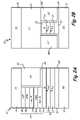
- FIGS. 6A and 6Bshow a schematic cross section and air bearing surface view of sensor 50 ′, respectively.
- Sensor 50 ′is structurally similar to sensor 40 ′ in FIGS. 4A and 4B in that reference layer assembly 22 is recessed from air bearing surface 100 wherein the space between reference layer assembly 22 and air bearing surface 100 is occupied by front shield 32 ′.
- Reference layer assembly 22is separated from freelayer assembly 16 by spacer layer 20 .
- seedlayer 14is under freelayer assembly 16 and freelayer and reference layer assemblies 16 and 22 are between top shield 36 , bottom shields 12 A, 12 B, and side shields 38 A′ and 38 B′.
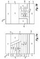
- FIGS. 8A and 8Bshow a schematic cross section and air bearing surface view of sensor 60 ′, respectively.
- Sensor 60 ′is structurally similar to sensor 40 ′ in FIGS. 4A and 4B in that reference layer assembly 22 is recessed from air bearing surface 100 wherein the space between reference layer assembly 22 and air bearing surface 100 is occupied by front shield 32 ′.
- Reference layer assembly 22is separated from freelayer assembly 16 by spacer layer 20 .
- seedlayer 14is under freelayer assembly 16
- freelayer and reference layer assemblies 16 and 22are between top shield 36 , bottom shield 12 and side shields 38 A′ and 38 B′.
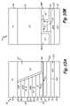
- the shield-to-shield spacingcan be as low as about 10 nm in sensor 70 ′.
- sensor 70 ′has an additional shield layer 12 A on shield layer 12 A extending away from MCS 100 until it abuts insulating layer 13 .
- the purpose of insulating layer 13is to restrict the electrical conduction path between top shield 36 and bottom shields 12 A and 12 B such that the current in the vicinity of MCS 100 is enhanced whereas the magnetization rotation due to the bit fields from the media transitions are larger. In doing so, the increased current will increase the signal output from sensor 70 ′.
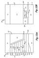
- the shield-to-shield spacing of sensor 80is similar to the shield-to-shield spacing of sensor 10 in FIGS. 1A and 1B , namely about 16 nm.
- the relative positions of freelayer assembly 16 and reference layer assembly 22may be reversed, so that reference layer assembly 22 is closer to bottom shield 12 .
- front shield 32may be positioned adjacent bottom shield 12 rather than top shield 36 .
Landscapes
- Physics & Mathematics (AREA)
- Engineering & Computer Science (AREA)
- Condensed Matter Physics & Semiconductors (AREA)
- General Physics & Mathematics (AREA)
- Chemical & Material Sciences (AREA)
- Nanotechnology (AREA)
- Crystallography & Structural Chemistry (AREA)
- Manufacturing & Machinery (AREA)
- Magnetic Heads (AREA)
- Hall/Mr Elements (AREA)
Abstract
Description
Claims (20)
Priority Applications (2)
| Application Number | Priority Date | Filing Date | Title |
|---|---|---|---|
| US12/405,051US8395867B2 (en) | 2009-03-16 | 2009-03-16 | Magnetic sensor with a recessed reference layer assembly and a front shield |
| PCT/US2010/027510WO2010107813A1 (en) | 2009-03-16 | 2010-03-16 | Magnetic sensor with a recessed reference layer assembly and a front shield |
Applications Claiming Priority (1)
| Application Number | Priority Date | Filing Date | Title |
|---|---|---|---|
| US12/405,051US8395867B2 (en) | 2009-03-16 | 2009-03-16 | Magnetic sensor with a recessed reference layer assembly and a front shield |
Publications (2)
| Publication Number | Publication Date |
|---|---|
| US20100232072A1 US20100232072A1 (en) | 2010-09-16 |
| US8395867B2true US8395867B2 (en) | 2013-03-12 |
Family
ID=42153856
Family Applications (1)
| Application Number | Title | Priority Date | Filing Date |
|---|---|---|---|
| US12/405,051Active2032-01-11US8395867B2 (en) | 2009-03-16 | 2009-03-16 | Magnetic sensor with a recessed reference layer assembly and a front shield |
Country Status (2)
| Country | Link |
|---|---|
| US (1) | US8395867B2 (en) |
| WO (1) | WO2010107813A1 (en) |
Cited By (13)
| Publication number | Priority date | Publication date | Assignee | Title |
|---|---|---|---|---|
| US8737023B2 (en)* | 2012-10-15 | 2014-05-27 | Seagate Technology Llc | Magnetic reader with tuned anisotropy |
| US9001473B1 (en) | 2014-03-21 | 2015-04-07 | HGST Netherlands B.V. | TMR/CPP reader for narrow reader gap application |
| US9007729B1 (en) | 2014-04-29 | 2015-04-14 | HGST Netherlands B.V. | Reader sensor having a recessed antiferromagnetic (AFM) pinning layer |
| US9070382B2 (en)* | 2013-02-01 | 2015-06-30 | Seagate Technology Llc | Side shield pedestal for data readers |
| US9177588B2 (en) | 2014-01-17 | 2015-11-03 | HGST Netherlands B.V. | Recessed IRMN reader process |
| US9286921B1 (en)* | 2014-10-22 | 2016-03-15 | Seagate Technology Llc | Reader sensor structure having front bottom shield adjacent recessed AFM layer |
| US9361914B1 (en) | 2014-06-18 | 2016-06-07 | Western Digital (Fremont), Llc | Magnetic sensor with thin capping layer |
| US9514771B2 (en)* | 2015-03-30 | 2016-12-06 | Tdk Corporation | Magneto-resistive effect element with recessed antiferromagnetic layer |
| US9570100B1 (en)* | 2015-10-21 | 2017-02-14 | Western Digital Technologies, Inc. | Two-dimensional magnetic recording device with center shield stabilized by recessed AFM layer |
| US9634242B2 (en) | 2015-07-27 | 2017-04-25 | Seagate Technology Llc | Data reader with front shield coupling structure |
| US9653102B1 (en) | 2014-12-19 | 2017-05-16 | Seagate Technology Llc | Data reader with pinned front shield |
| US9715892B1 (en) | 2015-07-31 | 2017-07-25 | Seagate Technology Llc | Data reader shield seed buffer |
| US10614840B1 (en)* | 2017-07-11 | 2020-04-07 | Seagate Technology Llc | Reader with shape optimized for higher SNR |
Families Citing this family (29)
| Publication number | Priority date | Publication date | Assignee | Title |
|---|---|---|---|---|
| US8792206B2 (en)* | 2009-05-18 | 2014-07-29 | Seagate Technology Llc | Method and apparatus for controlled front shield thickness for perpendicular writer |
| US8125746B2 (en)* | 2009-07-13 | 2012-02-28 | Seagate Technology Llc | Magnetic sensor with perpendicular anisotrophy free layer and side shields |
| US8705213B2 (en)* | 2010-02-26 | 2014-04-22 | Seagate Technology Llc | Magnetic field detecting device with shielding layer at least partially surrounding magnetoresistive stack |
| US8953285B2 (en)* | 2010-05-05 | 2015-02-10 | Headway Technologies, Inc. | Side shielded magnetoresistive (MR) read head with perpendicular magnetic free layer |
| CN102280574B (en)* | 2011-01-07 | 2014-04-16 | 江苏多维科技有限公司 | Thin film magnetoresistance sensing element, combination of multiple sensing elements, and electronic device coupled with combination |
| US8771847B2 (en)* | 2011-10-14 | 2014-07-08 | Seagate Technology | Reader stop-layers |
| US8675318B1 (en) | 2011-11-22 | 2014-03-18 | Western Digital (Fremont), Llc | Method and system for providing a read transducer having a reduced shield-to-shield spacing |
| US8711528B1 (en) | 2012-06-29 | 2014-04-29 | Western Digital (Fremont), Llc | Tunnel magnetoresistance read head with narrow shield-to-shield spacing |
| US9269382B1 (en) | 2012-06-29 | 2016-02-23 | Western Digital (Fremont), Llc | Method and system for providing a read transducer having improved pinning of the pinned layer at higher recording densities |
| US8760822B1 (en) | 2012-11-28 | 2014-06-24 | Western Digital (Fremont), Llc | Method and system for providing a read transducer having an extended pinned layer and soft magnetic bias structures with improved stability |
| US20140355152A1 (en)* | 2013-05-29 | 2014-12-04 | HGST Netherlands B.V. | Interlayer coupled free layer with out of plane magnetic orientation for magnetic read head |
| US9196267B2 (en)* | 2013-06-28 | 2015-11-24 | Seagate Technology Llc | Data writer with flux density insert |
| US9318130B1 (en) | 2013-07-02 | 2016-04-19 | Western Digital (Fremont), Llc | Method to fabricate tunneling magnetic recording heads with extended pinned layer |
| US9305578B1 (en) | 2013-08-01 | 2016-04-05 | Seagate Technology Llc | Magnetic element with reduced shield-to-shield spacing |
| US9214172B2 (en) | 2013-10-23 | 2015-12-15 | Western Digital (Fremont), Llc | Method of manufacturing a magnetic read head |
| US9269383B1 (en)* | 2015-01-23 | 2016-02-23 | HGST Netherlands B.V. | Multi-sensor (MIMO) head having a back side antiferromagnetic middle shield |
| US9478238B1 (en)* | 2015-03-30 | 2016-10-25 | Tdk Corporation | Magneto-resistive effect element with recessed antiferromagnetic layer |
| US9147404B1 (en) | 2015-03-31 | 2015-09-29 | Western Digital (Fremont), Llc | Method and system for providing a read transducer having a dual free layer |
| US9552834B1 (en)* | 2015-09-28 | 2017-01-24 | Seagate Technology Llc | Stabilization of one or more upper sensors in multi-sensor readers |
| JP6581516B2 (en)* | 2016-01-26 | 2019-09-25 | 株式会社東芝 | Magnetic sensor and magnetic sensor device |
| US9747933B1 (en)* | 2016-02-16 | 2017-08-29 | Tdk Corporation | Magneto-resistive effect element having side shield integrated with upper shield |
| US9767834B1 (en)* | 2016-03-18 | 2017-09-19 | Tdk Corporation | Magnetic head comprising magneto-resistance effect element and side shields |
| KR102182095B1 (en)* | 2016-07-12 | 2020-11-24 | 한양대학교 산학협력단 | 3-Dimensional Magneto-Sensor |
| US9799357B1 (en)* | 2016-11-08 | 2017-10-24 | Headway Technologies, Inc. | Magnetic reader sensor with shield spacing improvement and better pin flop robustness |
| JP2019103084A (en) | 2017-12-07 | 2019-06-24 | Tdk株式会社 | Magnetic resistance effect device |
| JP2019179902A (en) | 2018-03-30 | 2019-10-17 | Tdk株式会社 | Magnetoresistance effect device |
| JP2019179901A (en)* | 2018-03-30 | 2019-10-17 | Tdk株式会社 | Magnetoresistance effect device |
| DE102020006987B3 (en)* | 2020-11-09 | 2021-10-14 | Leibniz-Institut für Photonische Technologien e.V. (Engl.Leibniz Institute of Photonic Technology) | Magnetic system for counting revolutions with increased immunity to magnetic interference |
| US11758819B2 (en) | 2020-12-15 | 2023-09-12 | International Business Machines Corporation | Magneto-resistive random access memory with laterally-recessed free layer |
Citations (28)
| Publication number | Priority date | Publication date | Assignee | Title |
|---|---|---|---|---|
| US20030123198A1 (en)* | 2001-08-30 | 2003-07-03 | Nobuhiro Sugawara | Magnetic sensor using magneto-resistive effect, a magnetic head using magneto-resistive effect, a magnetic reproducing apparatus, a method of manufacturing a magnetic sensor using magneto-resistive effect and a method of manufacturing a magnetic head using magneto-resistive effect |
| US20030151857A1 (en)* | 2002-02-12 | 2003-08-14 | Fujitsu Limited | Flux guide type device, head having the same, and drive |
| US6667862B2 (en) | 2001-02-20 | 2003-12-23 | Carnegie Mellon University | Magnetoresistive read head having permanent magnet on top of magnetoresistive element |
| US6721139B2 (en)* | 2001-05-31 | 2004-04-13 | International Business Machines Corporation | Tunnel valve sensor with narrow gap flux guide employing a lamination of FeN and NiFeMo |
| US6738236B1 (en) | 1998-05-07 | 2004-05-18 | Seagate Technology Llc | Spin valve/GMR sensor using synthetic antiferromagnetic layer pinned by Mn-alloy having a high blocking temperature |
| US6847510B2 (en)* | 2002-09-27 | 2005-01-25 | Hitachi Global Storage Technologies Netherlands B.V. | Magnetic tunnel junction device with bottom free layer and improved underlayer |
| US20050128651A1 (en) | 2003-12-16 | 2005-06-16 | Seagate Technology Llc | Spin polarization enhancement artificial magnet |
| US20050168317A1 (en) | 2004-02-04 | 2005-08-04 | Seagate Technology Llc | TMR sensor with oxidized alloy barrier layer and method for forming the same |
| US6943993B2 (en)* | 2003-02-11 | 2005-09-13 | Western Digital (Fremont), Inc. | Magnetic recording head with a side shield structure for controlling side reading of thin film read sensor |
| US20050249979A1 (en)* | 2004-05-05 | 2005-11-10 | Hitachi Global Storage Technologies | High Hc pinned self-pinned sensor |
| US7027272B2 (en)* | 2000-12-04 | 2006-04-11 | Sony Corporation | Magnetoresistance effect device, and magnetoresistance effect magnetic head |
| US7035062B1 (en) | 2001-11-29 | 2006-04-25 | Seagate Technology Llc | Structure to achieve sensitivity and linear density in tunneling GMR heads using orthogonal magnetic alignments |
| US7092221B2 (en)* | 2003-12-12 | 2006-08-15 | Hitachi Global Storage Technologies Netherlands, B.V. | Top CPP GMR/TV with back end of stripe pinned by insulating AFM |
| US20070035888A1 (en) | 2004-04-02 | 2007-02-15 | Tdk Corporation | Stabilizer for magnetoresistive head and method of manufacture |
| US20070091513A1 (en) | 2004-04-02 | 2007-04-26 | Tdk Corporation | Stabilized spin valve head and method of manufacture |
| US20070230066A1 (en)* | 2006-03-28 | 2007-10-04 | Hitachi Global Storage Technologies | Current perpendicular to plane (CPP) magnetoresistive sensor having a flux guide structure and synthetic free layer |
| US20070253107A1 (en) | 2006-04-27 | 2007-11-01 | Hitachi Global Storage Technologies Netherlands B.V. | Perpendicular recording magnetic head |
| US7324310B2 (en)* | 2004-04-30 | 2008-01-29 | Hitachi Global Storage Technologies Netherlands B.V. | Self-pinned dual CPP sensor exchange pinned at stripe back-end to avoid amplitude flipping |
| US20080112087A1 (en) | 2006-11-14 | 2008-05-15 | Seagate Technology Llc | WAMR writer with an integrated spin momentum transfer driven oscillator for generating a microwave assist field |
| US7385842B2 (en) | 2003-12-29 | 2008-06-10 | Micron Technology, Inc. | Magnetic memory having synthetic antiferromagnetic pinned layer |
| US20080231994A1 (en) | 2007-03-22 | 2008-09-25 | Wataru Kimura | Perpendicular recording magnetic head |
| US20080259498A1 (en) | 2007-04-19 | 2008-10-23 | Hitachi Global Storage Technologies | Perpendicular write head with independent trailing shield designs |
| US7580230B2 (en)* | 2006-10-24 | 2009-08-25 | Hitachi Global Storage Technologies Netherlands B.V. | Magnetoresistive sensor having shape enhanced pinning, a flux guide structure and damage free virtual edges |
| US20090231762A1 (en)* | 2008-03-13 | 2009-09-17 | Tdk Corporation | Magnetoresistive effect element and thin-film magnetic head with the magnetoresistive effect element |
| US20090289207A1 (en) | 2008-03-27 | 2009-11-26 | Fabian Mauricio Barreda | Airflow regulating valve assembly |
| US20100187120A1 (en) | 2009-01-27 | 2010-07-29 | Seagate Technology Llc | Direct electrodeposition of magnetic recording head features |
| US20100321835A1 (en) | 2009-06-22 | 2010-12-23 | Seagate Technology Llc | Self-aligned, trailing edge partial side shield and method of making |
| US7961440B2 (en)* | 2007-09-27 | 2011-06-14 | Hitachi Global Storage Technologies Netherlands B.V. | Current perpendicular to plane magnetoresistive sensor with reduced read gap |
- 2009
- 2009-03-16USUS12/405,051patent/US8395867B2/enactiveActive
- 2010
- 2010-03-16WOPCT/US2010/027510patent/WO2010107813A1/enactiveApplication Filing
Patent Citations (28)
| Publication number | Priority date | Publication date | Assignee | Title |
|---|---|---|---|---|
| US6738236B1 (en) | 1998-05-07 | 2004-05-18 | Seagate Technology Llc | Spin valve/GMR sensor using synthetic antiferromagnetic layer pinned by Mn-alloy having a high blocking temperature |
| US7027272B2 (en)* | 2000-12-04 | 2006-04-11 | Sony Corporation | Magnetoresistance effect device, and magnetoresistance effect magnetic head |
| US6667862B2 (en) | 2001-02-20 | 2003-12-23 | Carnegie Mellon University | Magnetoresistive read head having permanent magnet on top of magnetoresistive element |
| US6721139B2 (en)* | 2001-05-31 | 2004-04-13 | International Business Machines Corporation | Tunnel valve sensor with narrow gap flux guide employing a lamination of FeN and NiFeMo |
| US20030123198A1 (en)* | 2001-08-30 | 2003-07-03 | Nobuhiro Sugawara | Magnetic sensor using magneto-resistive effect, a magnetic head using magneto-resistive effect, a magnetic reproducing apparatus, a method of manufacturing a magnetic sensor using magneto-resistive effect and a method of manufacturing a magnetic head using magneto-resistive effect |
| US7035062B1 (en) | 2001-11-29 | 2006-04-25 | Seagate Technology Llc | Structure to achieve sensitivity and linear density in tunneling GMR heads using orthogonal magnetic alignments |
| US20030151857A1 (en)* | 2002-02-12 | 2003-08-14 | Fujitsu Limited | Flux guide type device, head having the same, and drive |
| US6847510B2 (en)* | 2002-09-27 | 2005-01-25 | Hitachi Global Storage Technologies Netherlands B.V. | Magnetic tunnel junction device with bottom free layer and improved underlayer |
| US6943993B2 (en)* | 2003-02-11 | 2005-09-13 | Western Digital (Fremont), Inc. | Magnetic recording head with a side shield structure for controlling side reading of thin film read sensor |
| US7092221B2 (en)* | 2003-12-12 | 2006-08-15 | Hitachi Global Storage Technologies Netherlands, B.V. | Top CPP GMR/TV with back end of stripe pinned by insulating AFM |
| US20050128651A1 (en) | 2003-12-16 | 2005-06-16 | Seagate Technology Llc | Spin polarization enhancement artificial magnet |
| US7385842B2 (en) | 2003-12-29 | 2008-06-10 | Micron Technology, Inc. | Magnetic memory having synthetic antiferromagnetic pinned layer |
| US20050168317A1 (en) | 2004-02-04 | 2005-08-04 | Seagate Technology Llc | TMR sensor with oxidized alloy barrier layer and method for forming the same |
| US20070091513A1 (en) | 2004-04-02 | 2007-04-26 | Tdk Corporation | Stabilized spin valve head and method of manufacture |
| US20070035888A1 (en) | 2004-04-02 | 2007-02-15 | Tdk Corporation | Stabilizer for magnetoresistive head and method of manufacture |
| US7324310B2 (en)* | 2004-04-30 | 2008-01-29 | Hitachi Global Storage Technologies Netherlands B.V. | Self-pinned dual CPP sensor exchange pinned at stripe back-end to avoid amplitude flipping |
| US20050249979A1 (en)* | 2004-05-05 | 2005-11-10 | Hitachi Global Storage Technologies | High Hc pinned self-pinned sensor |
| US20070230066A1 (en)* | 2006-03-28 | 2007-10-04 | Hitachi Global Storage Technologies | Current perpendicular to plane (CPP) magnetoresistive sensor having a flux guide structure and synthetic free layer |
| US20070253107A1 (en) | 2006-04-27 | 2007-11-01 | Hitachi Global Storage Technologies Netherlands B.V. | Perpendicular recording magnetic head |
| US7580230B2 (en)* | 2006-10-24 | 2009-08-25 | Hitachi Global Storage Technologies Netherlands B.V. | Magnetoresistive sensor having shape enhanced pinning, a flux guide structure and damage free virtual edges |
| US20080112087A1 (en) | 2006-11-14 | 2008-05-15 | Seagate Technology Llc | WAMR writer with an integrated spin momentum transfer driven oscillator for generating a microwave assist field |
| US20080231994A1 (en) | 2007-03-22 | 2008-09-25 | Wataru Kimura | Perpendicular recording magnetic head |
| US20080259498A1 (en) | 2007-04-19 | 2008-10-23 | Hitachi Global Storage Technologies | Perpendicular write head with independent trailing shield designs |
| US7961440B2 (en)* | 2007-09-27 | 2011-06-14 | Hitachi Global Storage Technologies Netherlands B.V. | Current perpendicular to plane magnetoresistive sensor with reduced read gap |
| US20090231762A1 (en)* | 2008-03-13 | 2009-09-17 | Tdk Corporation | Magnetoresistive effect element and thin-film magnetic head with the magnetoresistive effect element |
| US20090289207A1 (en) | 2008-03-27 | 2009-11-26 | Fabian Mauricio Barreda | Airflow regulating valve assembly |
| US20100187120A1 (en) | 2009-01-27 | 2010-07-29 | Seagate Technology Llc | Direct electrodeposition of magnetic recording head features |
| US20100321835A1 (en) | 2009-06-22 | 2010-12-23 | Seagate Technology Llc | Self-aligned, trailing edge partial side shield and method of making |
Non-Patent Citations (1)
| Title |
|---|
| The International Search Report and Written Opinion of the International Searching Authority in counterpart foreign application No. PCT/US2010/027510 filed Mar. 16, 2010. |
Cited By (16)
| Publication number | Priority date | Publication date | Assignee | Title |
|---|---|---|---|---|
| US8737023B2 (en)* | 2012-10-15 | 2014-05-27 | Seagate Technology Llc | Magnetic reader with tuned anisotropy |
| US9070382B2 (en)* | 2013-02-01 | 2015-06-30 | Seagate Technology Llc | Side shield pedestal for data readers |
| US9177588B2 (en) | 2014-01-17 | 2015-11-03 | HGST Netherlands B.V. | Recessed IRMN reader process |
| US9001473B1 (en) | 2014-03-21 | 2015-04-07 | HGST Netherlands B.V. | TMR/CPP reader for narrow reader gap application |
| US9007729B1 (en) | 2014-04-29 | 2015-04-14 | HGST Netherlands B.V. | Reader sensor having a recessed antiferromagnetic (AFM) pinning layer |
| US9361914B1 (en) | 2014-06-18 | 2016-06-07 | Western Digital (Fremont), Llc | Magnetic sensor with thin capping layer |
| US9286921B1 (en)* | 2014-10-22 | 2016-03-15 | Seagate Technology Llc | Reader sensor structure having front bottom shield adjacent recessed AFM layer |
| US9899045B2 (en) | 2014-12-19 | 2018-02-20 | Seagate Technology Llc | Data reader with pinned front shield |
| US9653102B1 (en) | 2014-12-19 | 2017-05-16 | Seagate Technology Llc | Data reader with pinned front shield |
| US9514771B2 (en)* | 2015-03-30 | 2016-12-06 | Tdk Corporation | Magneto-resistive effect element with recessed antiferromagnetic layer |
| US9634242B2 (en) | 2015-07-27 | 2017-04-25 | Seagate Technology Llc | Data reader with front shield coupling structure |
| US10186285B2 (en) | 2015-07-27 | 2019-01-22 | Seagate Technology Llc | Data reader with front shield coupling structure |
| US9715892B1 (en) | 2015-07-31 | 2017-07-25 | Seagate Technology Llc | Data reader shield seed buffer |
| US9570100B1 (en)* | 2015-10-21 | 2017-02-14 | Western Digital Technologies, Inc. | Two-dimensional magnetic recording device with center shield stabilized by recessed AFM layer |
| US10614840B1 (en)* | 2017-07-11 | 2020-04-07 | Seagate Technology Llc | Reader with shape optimized for higher SNR |
| US11004466B1 (en) | 2017-07-11 | 2021-05-11 | Seagate Technology Llc | Reader with shape optimized for higher SNR |
Also Published As
| Publication number | Publication date |
|---|---|
| WO2010107813A1 (en) | 2010-09-23 |
| US20100232072A1 (en) | 2010-09-16 |
Similar Documents
| Publication | Publication Date | Title |
|---|---|---|
| US8395867B2 (en) | Magnetic sensor with a recessed reference layer assembly and a front shield | |
| US8482883B2 (en) | Magnetic sensor with perpendicular anisotrophy free layer and side shields | |
| US7929258B2 (en) | Magnetic sensor including a free layer having perpendicular to the plane anisotropy | |
| CN102298932B (en) | There are at ABS place three layers of reader of restriction of current | |
| US6381107B1 (en) | Magneto-resistive tunnel junction head having a shield lead rear flux guide | |
| US6344954B1 (en) | Magneto-resistive tunnel junction head with specific flux guide structure | |
| JP3807254B2 (en) | Magnetoresistive effect element, magnetoresistive effect type magnetic sensor, and magnetoresistive effect type magnetic head | |
| KR101376207B1 (en) | Magnetic element with improved stability | |
| US20110007426A1 (en) | Trapezoidal back bias and trilayer reader geometry to enhance device performance | |
| US9041391B2 (en) | Partial magnetic biasing of magnetoresistive sensor | |
| US6680827B2 (en) | Dual spin valve CPP MR with flux guide between free layers thereof | |
| US20120161263A1 (en) | Current perpendicular to plane (CPP) magnetoresistive sensor having dual composition hard bias layer | |
| JP2002150512A (en) | Magnetoresistive element and magnetoresistive magnetic head | |
| JP4658659B2 (en) | Magnetoresistance effect element having CPP structure and method of forming the same | |
| JP2005339784A (en) | Cpp-gmr reproducing head, its manufacturing method and cpp-gmr element | |
| CN114325512A (en) | Magnetic field detection device | |
| JP2002025012A (en) | Magnetoresistive effect thin film magnetic head | |
| US6512660B1 (en) | Current perpendicular-to-the-plane magnetoresistance read head with longitudinal or transverse bias provided by current | |
| US6791805B2 (en) | Current-perpendicular-to-plane spin valve reader with reduced scattering of majority spin electrons | |
| US7656620B2 (en) | Magnetic head device provided with lead electrode electrically connected to magnetic shield layer | |
| JP2002217473A (en) | Spin valve-type structure and method for forming it | |
| US20070127162A1 (en) | Magnetic head device provided with lead electrode electrically connected to upper shield layer and lower shield layer | |
| JP4939050B2 (en) | Method for forming magnetic free layer of magnetic tunnel junction element, tunnel junction read head and method for manufacturing the same | |
| JP2005328064A (en) | Magnetoresistance effect element and forming method therefor, and thin film magnetic head and manufacturing method therefor | |
| US7684159B2 (en) | Magnetic head device provided with lead electrode electrically connected to upper shield layer and lower shield layer |
Legal Events
| Date | Code | Title | Description |
|---|---|---|---|
| AS | Assignment | Owner name:SEAGATE TECHNOLOGY LLC, CALIFORNIA Free format text:ASSIGNMENT OF ASSIGNORS INTEREST;ASSIGNORS:DIMITROV, DIMITAR VELIKOV;GAO, ZHENG;JUNG, WONJOON;AND OTHERS;REEL/FRAME:022403/0094 Effective date:20090316 | |
| AS | Assignment | Owner name:WELLS FARGO BANK, NATIONAL ASSOCIATION, AS COLLATERAL AGENT AND SECOND PRIORITY REPRESENTATIVE, CALIFORNIA Free format text:SECURITY AGREEMENT;ASSIGNORS:MAXTOR CORPORATION;SEAGATE TECHNOLOGY LLC;SEAGATE TECHNOLOGY INTERNATIONAL;REEL/FRAME:022757/0017 Effective date:20090507 Owner name:JPMORGAN CHASE BANK, N.A., AS ADMINISTRATIVE AGENT AND FIRST PRIORITY REPRESENTATIVE, NEW YORK Free format text:SECURITY AGREEMENT;ASSIGNORS:MAXTOR CORPORATION;SEAGATE TECHNOLOGY LLC;SEAGATE TECHNOLOGY INTERNATIONAL;REEL/FRAME:022757/0017 Effective date:20090507 Owner name:JPMORGAN CHASE BANK, N.A., AS ADMINISTRATIVE AGENT Free format text:SECURITY AGREEMENT;ASSIGNORS:MAXTOR CORPORATION;SEAGATE TECHNOLOGY LLC;SEAGATE TECHNOLOGY INTERNATIONAL;REEL/FRAME:022757/0017 Effective date:20090507 Owner name:WELLS FARGO BANK, NATIONAL ASSOCIATION, AS COLLATE Free format text:SECURITY AGREEMENT;ASSIGNORS:MAXTOR CORPORATION;SEAGATE TECHNOLOGY LLC;SEAGATE TECHNOLOGY INTERNATIONAL;REEL/FRAME:022757/0017 Effective date:20090507 | |
| AS | Assignment | Owner name:SEAGATE TECHNOLOGY HDD HOLDINGS, CALIFORNIA Free format text:RELEASE;ASSIGNOR:JPMORGAN CHASE BANK, N.A., AS ADMINISTRATIVE AGENT;REEL/FRAME:025662/0001 Effective date:20110114 Owner name:SEAGATE TECHNOLOGY LLC, CALIFORNIA Free format text:RELEASE;ASSIGNOR:JPMORGAN CHASE BANK, N.A., AS ADMINISTRATIVE AGENT;REEL/FRAME:025662/0001 Effective date:20110114 Owner name:SEAGATE TECHNOLOGY INTERNATIONAL, CALIFORNIA Free format text:RELEASE;ASSIGNOR:JPMORGAN CHASE BANK, N.A., AS ADMINISTRATIVE AGENT;REEL/FRAME:025662/0001 Effective date:20110114 Owner name:MAXTOR CORPORATION, CALIFORNIA Free format text:RELEASE;ASSIGNOR:JPMORGAN CHASE BANK, N.A., AS ADMINISTRATIVE AGENT;REEL/FRAME:025662/0001 Effective date:20110114 | |
| AS | Assignment | Owner name:THE BANK OF NOVA SCOTIA, AS ADMINISTRATIVE AGENT, CANADA Free format text:SECURITY AGREEMENT;ASSIGNOR:SEAGATE TECHNOLOGY LLC;REEL/FRAME:026010/0350 Effective date:20110118 Owner name:THE BANK OF NOVA SCOTIA, AS ADMINISTRATIVE AGENT, Free format text:SECURITY AGREEMENT;ASSIGNOR:SEAGATE TECHNOLOGY LLC;REEL/FRAME:026010/0350 Effective date:20110118 | |
| STCF | Information on status: patent grant | Free format text:PATENTED CASE | |
| AS | Assignment | Owner name:EVAULT INC. (F/K/A I365 INC.), CALIFORNIA Free format text:TERMINATION AND RELEASE OF SECURITY INTEREST IN PATENT RIGHTS;ASSIGNOR:WELLS FARGO BANK, NATIONAL ASSOCIATION, AS COLLATERAL AGENT AND SECOND PRIORITY REPRESENTATIVE;REEL/FRAME:030833/0001 Effective date:20130312 Owner name:SEAGATE TECHNOLOGY US HOLDINGS, INC., CALIFORNIA Free format text:TERMINATION AND RELEASE OF SECURITY INTEREST IN PATENT RIGHTS;ASSIGNOR:WELLS FARGO BANK, NATIONAL ASSOCIATION, AS COLLATERAL AGENT AND SECOND PRIORITY REPRESENTATIVE;REEL/FRAME:030833/0001 Effective date:20130312 Owner name:SEAGATE TECHNOLOGY LLC, CALIFORNIA Free format text:TERMINATION AND RELEASE OF SECURITY INTEREST IN PATENT RIGHTS;ASSIGNOR:WELLS FARGO BANK, NATIONAL ASSOCIATION, AS COLLATERAL AGENT AND SECOND PRIORITY REPRESENTATIVE;REEL/FRAME:030833/0001 Effective date:20130312 Owner name:SEAGATE TECHNOLOGY INTERNATIONAL, CAYMAN ISLANDS Free format text:TERMINATION AND RELEASE OF SECURITY INTEREST IN PATENT RIGHTS;ASSIGNOR:WELLS FARGO BANK, NATIONAL ASSOCIATION, AS COLLATERAL AGENT AND SECOND PRIORITY REPRESENTATIVE;REEL/FRAME:030833/0001 Effective date:20130312 | |
| CC | Certificate of correction | ||
| FPAY | Fee payment | Year of fee payment:4 | |
| MAFP | Maintenance fee payment | Free format text:PAYMENT OF MAINTENANCE FEE, 8TH YEAR, LARGE ENTITY (ORIGINAL EVENT CODE: M1552); ENTITY STATUS OF PATENT OWNER: LARGE ENTITY Year of fee payment:8 | |
| MAFP | Maintenance fee payment | Free format text:PAYMENT OF MAINTENANCE FEE, 12TH YEAR, LARGE ENTITY (ORIGINAL EVENT CODE: M1553); ENTITY STATUS OF PATENT OWNER: LARGE ENTITY Year of fee payment:12 | |
| AS | Assignment | Owner name:SEAGATE TECHNOLOGY PUBLIC LIMITED COMPANY, CALIFORNIA Free format text:RELEASE BY SECURED PARTY;ASSIGNOR:THE BANK OF NOVA SCOTIA;REEL/FRAME:072193/0001 Effective date:20250303 Owner name:SEAGATE TECHNOLOGY, CALIFORNIA Free format text:RELEASE BY SECURED PARTY;ASSIGNOR:THE BANK OF NOVA SCOTIA;REEL/FRAME:072193/0001 Effective date:20250303 Owner name:SEAGATE TECHNOLOGY HDD HOLDINGS, CALIFORNIA Free format text:RELEASE BY SECURED PARTY;ASSIGNOR:THE BANK OF NOVA SCOTIA;REEL/FRAME:072193/0001 Effective date:20250303 Owner name:I365 INC., CALIFORNIA Free format text:RELEASE BY SECURED PARTY;ASSIGNOR:THE BANK OF NOVA SCOTIA;REEL/FRAME:072193/0001 Effective date:20250303 Owner name:SEAGATE TECHNOLOGY LLC, CALIFORNIA Free format text:RELEASE BY SECURED PARTY;ASSIGNOR:THE BANK OF NOVA SCOTIA;REEL/FRAME:072193/0001 Effective date:20250303 Owner name:SEAGATE TECHNOLOGY INTERNATIONAL, CAYMAN ISLANDS Free format text:RELEASE BY SECURED PARTY;ASSIGNOR:THE BANK OF NOVA SCOTIA;REEL/FRAME:072193/0001 Effective date:20250303 Owner name:SEAGATE HDD CAYMAN, CAYMAN ISLANDS Free format text:RELEASE BY SECURED PARTY;ASSIGNOR:THE BANK OF NOVA SCOTIA;REEL/FRAME:072193/0001 Effective date:20250303 Owner name:SEAGATE TECHNOLOGY (US) HOLDINGS, INC., CALIFORNIA Free format text:RELEASE BY SECURED PARTY;ASSIGNOR:THE BANK OF NOVA SCOTIA;REEL/FRAME:072193/0001 Effective date:20250303 |