US8395562B2 - Antenna module for portable electronic device - Google Patents
Antenna module for portable electronic deviceDownload PDFInfo
- Publication number
- US8395562B2 US8395562B2US12/844,989US84498910AUS8395562B2US 8395562 B2US8395562 B2US 8395562B2US 84498910 AUS84498910 AUS 84498910AUS 8395562 B2US8395562 B2US 8395562B2
- Authority
- US
- United States
- Prior art keywords
- radiating
- radiating section
- electronic device
- loop portion
- portable electronic
- Prior art date
- Legal status (The legal status is an assumption and is not a legal conclusion. Google has not performed a legal analysis and makes no representation as to the accuracy of the status listed.)
- Expired - Fee Related, expires
Links
Images


Classifications
- H—ELECTRICITY
- H01—ELECTRIC ELEMENTS
- H01Q—ANTENNAS, i.e. RADIO AERIALS
- H01Q9/00—Electrically-short antennas having dimensions not more than twice the operating wavelength and consisting of conductive active radiating elements
- H01Q9/04—Resonant antennas
- H01Q9/16—Resonant antennas with feed intermediate between the extremities of the antenna, e.g. centre-fed dipole
- H01Q9/26—Resonant antennas with feed intermediate between the extremities of the antenna, e.g. centre-fed dipole with folded element or elements, the folded parts being spaced apart a small fraction of operating wavelength
- H—ELECTRICITY
- H01—ELECTRIC ELEMENTS
- H01Q—ANTENNAS, i.e. RADIO AERIALS
- H01Q1/00—Details of, or arrangements associated with, antennas
- H01Q1/12—Supports; Mounting means
- H01Q1/22—Supports; Mounting means by structural association with other equipment or articles
- H01Q1/24—Supports; Mounting means by structural association with other equipment or articles with receiving set
- H01Q1/241—Supports; Mounting means by structural association with other equipment or articles with receiving set used in mobile communications, e.g. GSM
- H01Q1/242—Supports; Mounting means by structural association with other equipment or articles with receiving set used in mobile communications, e.g. GSM specially adapted for hand-held use
- H01Q1/243—Supports; Mounting means by structural association with other equipment or articles with receiving set used in mobile communications, e.g. GSM specially adapted for hand-held use with built-in antennas
- H—ELECTRICITY
- H01—ELECTRIC ELEMENTS
- H01Q—ANTENNAS, i.e. RADIO AERIALS
- H01Q5/00—Arrangements for simultaneous operation of antennas on two or more different wavebands, e.g. dual-band or multi-band arrangements
- H01Q5/30—Arrangements for providing operation on different wavebands
- H01Q5/307—Individual or coupled radiating elements, each element being fed in an unspecified way
- H01Q5/342—Individual or coupled radiating elements, each element being fed in an unspecified way for different propagation modes
- H—ELECTRICITY
- H01—ELECTRIC ELEMENTS
- H01Q—ANTENNAS, i.e. RADIO AERIALS
- H01Q5/00—Arrangements for simultaneous operation of antennas on two or more different wavebands, e.g. dual-band or multi-band arrangements
- H01Q5/40—Imbricated or interleaved structures; Combined or electromagnetically coupled arrangements, e.g. comprising two or more non-connected fed radiating elements
- H—ELECTRICITY
- H01—ELECTRIC ELEMENTS
- H01Q—ANTENNAS, i.e. RADIO AERIALS
- H01Q7/00—Loop antennas with a substantially uniform current distribution around the loop and having a directional radiation pattern in a plane perpendicular to the plane of the loop
- H—ELECTRICITY
- H01—ELECTRIC ELEMENTS
- H01Q—ANTENNAS, i.e. RADIO AERIALS
- H01Q9/00—Electrically-short antennas having dimensions not more than twice the operating wavelength and consisting of conductive active radiating elements
- H01Q9/04—Resonant antennas
- H01Q9/16—Resonant antennas with feed intermediate between the extremities of the antenna, e.g. centre-fed dipole
- H01Q9/28—Conical, cylindrical, cage, strip, gauze, or like elements having an extended radiating surface; Elements comprising two conical surfaces having collinear axes and adjacent apices and fed by two-conductor transmission lines
- H01Q9/285—Planar dipole
Definitions
- the disclosuregenerally relates to antenna modules, particularly to a miniaturized antenna module and a portable electronic device using the antenna module.
- Antennasare usually assembled inside a portable electronic device to send and receive signals.
- the antennasoften occupy a large amount of space within the portable electronic device.
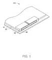
- FIG. 1is partially, schematic view of a portable electronic device employed with an antenna module, according to one exemplary embodiment.
- FIG. 2is an exploded view of the portable electronic device of FIG. 1 .
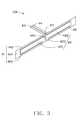
- FIG. 3is a schematic view of the antenna module of FIG. 1 .
- FIG. 4is a schematic view of exemplary dimensions of an exemplary embodiment of the antenna module of FIG. 1 .
- FIG. 5is a test graph obtained from the antenna module of FIG. 1 , disclosing return loss varying with frequency, when the lengths of the first and second radiating arm are changed.
- FIG. 6is a test graph obtained from the antenna module of FIG. 1 , disclosing return loss varying with frequency, when the length of the loop portion is lengthened.
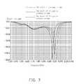
- FIG. 7is a test graph obtained from the antenna module of FIG. 1 , disclosing return loss varying with frequency, when width of the gap is widened.
- FIGS. 1 and 2show an exemplary embodiment of a portable electronic device 100 such as a mobile phone and a personal digital assistant (PDA) including a housing 10 (partially shown), a circuit board 20 (partially shown), a substrate 30 and an antenna module 40 .
- the circuit board 20 and the substrate 30are mounted inside the housing 10 .
- the antenna module 40is attached to the substrate 30 and connected to the circuit board 20 .
- the housing 10can be a portion of a cover of the portable electronic device 100 .
- the circuit board 20is mounted inside the housing 10 and includes a feeding point 21 (schematically shown) and a grounding point 22 (schematically shown).
- the substrate 30includes a top surface 31 , a bottom surface 32 and a side surface 33 . The bottom of the substrate 30 is recessed to form a stepped mounting surface 34 .
- the antenna module 40includes a loop portion 41 , a dipole portion 42 , a feeding end portion 43 and a grounding end portion 44 .
- the loop portion 41is substantially a rectangular frame having an opening 411 .
- the loop portion 41includes a first radiating section 412 , a second radiating section 413 , and two connecting sections 414 .
- the second radiating section 413has substantially the same length and width as the first radiating section 412 .
- the first and second radiating section 412 and 413are parallel with each other.
- the two connecting sections 414connect to ends of the first and second radiating section 412 , 413 and form the frame loop portion 40 with the first and second radiating section 412 , 413 .
- the opening 411is defined in a middle portion of the first radiating section 412 .
- the dipole portion 42includes a first radiating arm 421 , a second radiating arm 422 , and two connecting ends 423 .
- the length and width of the first and second radiating arm 421are the same as that of the second radiating arm 422 in this exemplary embodiment.
- the first radiating arm 421 and the second radiating arm 422are arranged in a line and cooperatively define a slot 424 therebetween.
- the two connecting ends 423are positioned at one side of the first and second radiating arm 421 , 422 . Each connecting end 423 is connected to one of the first and second radiating arm 421 , 422 .
- the dipole portion 42is positioned in the loop portion 41 .
- Two distal ends of the connecting ends 423 opposite to the first and second radiating arm 421 , 422are connected to the second radiating section 413 of the loop portion 41 .
- the slot 424communicates with the opening 411 .
- the length of each of the first and second arms 421 , 422is slightly less than 1 ⁇ 2 the length of the first radiating section 412 ; the width of the first and second arms 421 , 422 is slightly less than the width of the connecting ends 414 . Therefore, two substantially U-shaped gaps 45 are formed between the loop portion 41 and the dipole portion 42 .
- the length and width of the loop portion 41are 68 mm and 9.6 mm, respectively.
- the length and width of the first and second radiating armare 25.3 mm and 4.2 mm, respectively.
- the width of the gap 45 between the dipole portion 42 and loop portion 41is 0.5 mm.
- the width of the slot 424 and the opening 411is 1 mm.
- the feeding end portion 43 and the grounding end portion 43are both rectangular sheets connecting to the feeding point 21 and the grounding point 22 of the circuit board 20 , respectively.
- the circuit board 20 and the substrate 30are mounted inside the housing 10 .
- the mounting surface 34 of the substrate 30is attached to the circuit board 20 and supported by the circuit board 20 .
- the antenna module 40is mounted on the substrate 30 .
- the feeding end portion 43 and the grounding end portion 44are attached on the top surface 31 and respectively connected to the feeding point 21 and the grounding point 22 .
- the loop portion 41 and the dipole portion 42are attached on the side surface 32 .
- the portable electronic device 100may work at a first frequency band of about 824 MHz-894 MHz and a second frequency band of about 1710 MHz-2170 MHz, which are suitable for different communication systems.
- the length of the first radiating arm 421 and the second radiating arm 422can be changed, such as the length of the first radiating arm 421 can be made slightly longer than the length of the second radiating arm 422 .
- the length of the loop portion 41can be changed.
- the center of the first frequency bandis adjusted from about 860 MHz to about 830 MHz; when the length of the first radiating section 412 and the second radiating section 413 are lengthened by 5 mm, the center of the first frequency band is adjusted from about 860 MHz to about 810 MHz.
- the width of the slot 424 between the first radiating arm 421 and the second radiating arm 422can be changed to adjust the second frequency band of the antenna module 40 .
- the center of the second frequency bandis adjusted from about 2170 MHz to about 2014 MHz; when the width of the slot 424 is widened by 4 mm, the center of the second frequency band is adjusted from about 2170 MHz to about 2090 MHz.
- the antenna module 40 with the combination of the loop portion 41 and the dipole portion 42are miniaturized, having the first and second frequency bands for different communication systems.
Landscapes
- Physics & Mathematics (AREA)
- Electromagnetism (AREA)
- Engineering & Computer Science (AREA)
- Computer Networks & Wireless Communication (AREA)
- Variable-Direction Aerials And Aerial Arrays (AREA)
- Support Of Aerials (AREA)
- Details Of Aerials (AREA)
Abstract
Description
Claims (16)
Applications Claiming Priority (2)
| Application Number | Priority Date | Filing Date | Title |
|---|---|---|---|
| TW099116597ATWI513110B (en) | 2010-05-25 | 2010-05-25 | Antenna module and wireless communication device using the same |
| TW99116597 | 2010-05-25 |
Publications (2)
| Publication Number | Publication Date |
|---|---|
| US20110291906A1 US20110291906A1 (en) | 2011-12-01 |
| US8395562B2true US8395562B2 (en) | 2013-03-12 |
Family
ID=45021655
Family Applications (1)
| Application Number | Title | Priority Date | Filing Date |
|---|---|---|---|
| US12/844,989Expired - Fee RelatedUS8395562B2 (en) | 2010-05-25 | 2010-07-28 | Antenna module for portable electronic device |
Country Status (3)
| Country | Link |
|---|---|
| US (1) | US8395562B2 (en) |
| JP (1) | JP2011250396A (en) |
| TW (1) | TWI513110B (en) |
Families Citing this family (5)
| Publication number | Priority date | Publication date | Assignee | Title |
|---|---|---|---|---|
| TWI557990B (en)* | 2014-04-16 | 2016-11-11 | Mobile communication device | |
| CN106486762B (en)* | 2015-08-31 | 2019-12-10 | 宇龙计算机通信科技(深圳)有限公司 | Antenna device and terminal |
| CN105428786B (en)* | 2015-11-09 | 2019-02-19 | 小米科技有限责任公司 | Antenna module and electronic equipment with metal edge frame |
| CN105846054B (en)* | 2016-01-29 | 2019-02-22 | 北京小米移动软件有限公司 | Terminal back cover and mobile terminal |
| USD981380S1 (en)* | 2021-06-25 | 2023-03-21 | Xerafy Inc. | Set of RFID antenna and protective cover |
Citations (4)
| Publication number | Priority date | Publication date | Assignee | Title |
|---|---|---|---|---|
| US5198826A (en)* | 1989-09-22 | 1993-03-30 | Nippon Sheet Glass Co., Ltd. | Wide-band loop antenna with outer and inner loop conductors |
| US7583235B2 (en)* | 2006-09-12 | 2009-09-01 | Samsung Electronics Co., Ltd. | Folded dipole loop antenna having matching circuit integrally formed therein |
| US20100103064A1 (en)* | 2008-10-23 | 2010-04-29 | Symbol Technologies, Inc. | Parasitic dipole assisted wlan antenna |
| US8207899B2 (en)* | 2005-11-18 | 2012-06-26 | Sony Mobile Communications Japan, Inc. | Folded dipole antenna device and mobile radio terminal |
- 2010
- 2010-05-25TWTW099116597Apatent/TWI513110B/ennot_activeIP Right Cessation
- 2010-07-28USUS12/844,989patent/US8395562B2/ennot_activeExpired - Fee Related
- 2011
- 2011-04-01JPJP2011081550Apatent/JP2011250396A/ennot_activeWithdrawn
Patent Citations (4)
| Publication number | Priority date | Publication date | Assignee | Title |
|---|---|---|---|---|
| US5198826A (en)* | 1989-09-22 | 1993-03-30 | Nippon Sheet Glass Co., Ltd. | Wide-band loop antenna with outer and inner loop conductors |
| US8207899B2 (en)* | 2005-11-18 | 2012-06-26 | Sony Mobile Communications Japan, Inc. | Folded dipole antenna device and mobile radio terminal |
| US7583235B2 (en)* | 2006-09-12 | 2009-09-01 | Samsung Electronics Co., Ltd. | Folded dipole loop antenna having matching circuit integrally formed therein |
| US20100103064A1 (en)* | 2008-10-23 | 2010-04-29 | Symbol Technologies, Inc. | Parasitic dipole assisted wlan antenna |
Also Published As
| Publication number | Publication date |
|---|---|
| US20110291906A1 (en) | 2011-12-01 |
| JP2011250396A (en) | 2011-12-08 |
| TW201143203A (en) | 2011-12-01 |
| TWI513110B (en) | 2015-12-11 |
Similar Documents
| Publication | Publication Date | Title |
|---|---|---|
| US9647320B2 (en) | Antenna assembly and electronic device using the antenna assembly | |
| US10511081B2 (en) | Antenna structure and wireless communication device using same | |
| US10186752B2 (en) | Antenna structure and wireless communication device using same | |
| US9806400B2 (en) | Antenna structure and wireless communication device using the antenna structure | |
| US8330657B2 (en) | Antenna and portable wireless communication device using the same | |
| US8013796B2 (en) | Dual-band antenna | |
| US8659492B2 (en) | Multiband antenna | |
| US20100052997A1 (en) | Antenna modules and portable electronic devices using the same | |
| US20110181480A1 (en) | Antenna module | |
| US20100253581A1 (en) | Multiband antenna and portable wireless communication device using the same | |
| US20180026336A1 (en) | Antenna structure and wireless communication device using same | |
| US9722294B2 (en) | Antenna structure and wireless communication device using the same | |
| US9425509B2 (en) | Antenna structure and wireless communication device using the same | |
| US20120162017A1 (en) | Multiband antenna | |
| US8373599B2 (en) | Antenna module, wireless communication device using the antenna module and method for adjusting a performance factor of the antenna module | |
| US8395562B2 (en) | Antenna module for portable electronic device | |
| US20120262342A1 (en) | Multiband antenna | |
| US20140361929A1 (en) | Antenna structure and wireless communication device using the same | |
| US9450295B2 (en) | Wireless communication device | |
| US9386132B2 (en) | Wireless communication device | |
| US9385417B2 (en) | Broadband antenna and wireless communication device employing same | |
| US9258025B2 (en) | Antenna structure and wireless communication device using the same | |
| US20140354488A1 (en) | Antenna structure and wireless communication device employing same | |
| US20120162043A1 (en) | Multiband antenna | |
| US9253296B2 (en) | Wireless communication device |
Legal Events
| Date | Code | Title | Description |
|---|---|---|---|
| AS | Assignment | Owner name:CHI MEI COMMUNICATION SYSTEMS, INC., TAIWAN Free format text:ASSIGNMENT OF ASSIGNORS INTEREST;ASSIGNORS:HSU, CHO-KANG;CHEN, YI-TING;REEL/FRAME:024752/0462 Effective date:20100723 | |
| STCF | Information on status: patent grant | Free format text:PATENTED CASE | |
| FPAY | Fee payment | Year of fee payment:4 | |
| MAFP | Maintenance fee payment | Free format text:PAYMENT OF MAINTENANCE FEE, 8TH YEAR, LARGE ENTITY (ORIGINAL EVENT CODE: M1552); ENTITY STATUS OF PATENT OWNER: LARGE ENTITY Year of fee payment:8 | |
| FEPP | Fee payment procedure | Free format text:MAINTENANCE FEE REMINDER MAILED (ORIGINAL EVENT CODE: REM.); ENTITY STATUS OF PATENT OWNER: LARGE ENTITY | |
| LAPS | Lapse for failure to pay maintenance fees | Free format text:PATENT EXPIRED FOR FAILURE TO PAY MAINTENANCE FEES (ORIGINAL EVENT CODE: EXP.); ENTITY STATUS OF PATENT OWNER: LARGE ENTITY | |
| STCH | Information on status: patent discontinuation | Free format text:PATENT EXPIRED DUE TO NONPAYMENT OF MAINTENANCE FEES UNDER 37 CFR 1.362 | |
| FP | Lapsed due to failure to pay maintenance fee | Effective date:20250312 |