US8395165B2 - Laterally contacted blue LED with superlattice current spreading layer - Google Patents
Laterally contacted blue LED with superlattice current spreading layerDownload PDFInfo
- Publication number
- US8395165B2 US8395165B2US13/178,497US201113178497AUS8395165B2US 8395165 B2US8395165 B2US 8395165B2US 201113178497 AUS201113178497 AUS 201113178497AUS 8395165 B2US8395165 B2US 8395165B2
- Authority
- US
- United States
- Prior art keywords
- layer
- gallium
- nitride
- type
- sublayer
- Prior art date
- Legal status (The legal status is an assumption and is not a legal conclusion. Google has not performed a legal analysis and makes no representation as to the accuracy of the status listed.)
- Expired - Fee Related, expires
Links
- 239000000758substrateSubstances0.000claimsabstractdescription47
- 229910052594sapphireInorganic materials0.000claimsabstractdescription25
- 239000010980sapphireSubstances0.000claimsabstractdescription25
- 229910052738indiumInorganic materials0.000claimsabstractdescription9
- APFVFJFRJDLVQX-UHFFFAOYSA-Nindium atomChemical compound[In]APFVFJFRJDLVQX-UHFFFAOYSA-N0.000claimsabstractdescription9
- 229910002601GaNInorganic materials0.000claimsdescription148
- JMASRVWKEDWRBT-UHFFFAOYSA-NGallium nitrideChemical compound[Ga]#NJMASRVWKEDWRBT-UHFFFAOYSA-N0.000claimsdescription118
- 238000000034methodMethods0.000claimsdescription9
- 229910052751metalInorganic materials0.000claimsdescription8
- 239000002184metalSubstances0.000claimsdescription8
- 239000000463materialSubstances0.000claimsdescription7
- 230000007547defectEffects0.000abstractdescription10
- 229910002704AlGaNInorganic materials0.000abstract1
- 239000010410layerSubstances0.000description174
- 238000010586diagramMethods0.000description6
- 229910052782aluminiumInorganic materials0.000description5
- XAGFODPZIPBFFR-UHFFFAOYSA-NaluminiumChemical compound[Al]XAGFODPZIPBFFR-UHFFFAOYSA-N0.000description5
- 229910052710siliconInorganic materials0.000description4
- 239000010703siliconSubstances0.000description4
- 239000002019doping agentSubstances0.000description3
- OAICVXFJPJFONN-UHFFFAOYSA-NPhosphorusChemical compound[P]OAICVXFJPJFONN-UHFFFAOYSA-N0.000description2
- 230000001066destructive effectEffects0.000description2
- 238000004519manufacturing processMethods0.000description2
- GYHNNYVSQQEPJS-UHFFFAOYSA-NGalliumChemical compound[Ga]GYHNNYVSQQEPJS-UHFFFAOYSA-N0.000description1
- FYYHWMGAXLPEAU-UHFFFAOYSA-NMagnesiumChemical compound[Mg]FYYHWMGAXLPEAU-UHFFFAOYSA-N0.000description1
- 230000006978adaptationEffects0.000description1
- PNEYBMLMFCGWSK-UHFFFAOYSA-Naluminium oxideInorganic materials[O-2].[O-2].[O-2].[Al+3].[Al+3]PNEYBMLMFCGWSK-UHFFFAOYSA-N0.000description1
- 230000015572biosynthetic processEffects0.000description1
- 239000011248coating agentSubstances0.000description1
- 238000000576coating methodMethods0.000description1
- 239000003086colorantSubstances0.000description1
- 239000000470constituentSubstances0.000description1
- PMHQVHHXPFUNSP-UHFFFAOYSA-Mcopper(1+);methylsulfanylmethane;bromideChemical compoundBr[Cu].CSCPMHQVHHXPFUNSP-UHFFFAOYSA-M0.000description1
- 229910052593corundumInorganic materials0.000description1
- 238000005530etchingMethods0.000description1
- 229910052733galliumInorganic materials0.000description1
- AMGQUBHHOARCQH-UHFFFAOYSA-Nindium;oxotinChemical compound[In].[Sn]=OAMGQUBHHOARCQH-UHFFFAOYSA-N0.000description1
- 229910052749magnesiumInorganic materials0.000description1
- 239000011777magnesiumSubstances0.000description1
- 238000012986modificationMethods0.000description1
- 230000004048modificationEffects0.000description1
- 238000005498polishingMethods0.000description1
- 230000005855radiationEffects0.000description1
- 239000004065semiconductorSubstances0.000description1
- 239000002356single layerSubstances0.000description1
- 239000007787solidSubstances0.000description1
- 239000000126substanceSubstances0.000description1
- 229910001845yogo sapphireInorganic materials0.000description1
Images


Classifications
- H—ELECTRICITY
- H10—SEMICONDUCTOR DEVICES; ELECTRIC SOLID-STATE DEVICES NOT OTHERWISE PROVIDED FOR
- H10H—INORGANIC LIGHT-EMITTING SEMICONDUCTOR DEVICES HAVING POTENTIAL BARRIERS
- H10H20/00—Individual inorganic light-emitting semiconductor devices having potential barriers, e.g. light-emitting diodes [LED]
- H10H20/80—Constructional details
- H10H20/81—Bodies
- H10H20/811—Bodies having quantum effect structures or superlattices, e.g. tunnel junctions
- H—ELECTRICITY
- H10—SEMICONDUCTOR DEVICES; ELECTRIC SOLID-STATE DEVICES NOT OTHERWISE PROVIDED FOR
- H10H—INORGANIC LIGHT-EMITTING SEMICONDUCTOR DEVICES HAVING POTENTIAL BARRIERS
- H10H20/00—Individual inorganic light-emitting semiconductor devices having potential barriers, e.g. light-emitting diodes [LED]
- H10H20/80—Constructional details
- H10H20/81—Bodies
- H10H20/822—Materials of the light-emitting regions
- H10H20/824—Materials of the light-emitting regions comprising only Group III-V materials, e.g. GaP
- H10H20/825—Materials of the light-emitting regions comprising only Group III-V materials, e.g. GaP containing nitrogen, e.g. GaN
- H—ELECTRICITY
- H10—SEMICONDUCTOR DEVICES; ELECTRIC SOLID-STATE DEVICES NOT OTHERWISE PROVIDED FOR
- H10H—INORGANIC LIGHT-EMITTING SEMICONDUCTOR DEVICES HAVING POTENTIAL BARRIERS
- H10H20/00—Individual inorganic light-emitting semiconductor devices having potential barriers, e.g. light-emitting diodes [LED]
- H10H20/80—Constructional details
- H10H20/81—Bodies
- H10H20/816—Bodies having carrier transport control structures, e.g. highly-doped semiconductor layers or current-blocking structures
Definitions
- the present disclosurerelates generally to laterally contacted GaN-based blue LEDs.
- a Light Emitting Diodeis a solid state device that converts electrical energy to light. Light is emitted from an active layer of semiconductor materials sandwiched between oppositely doped layers when a voltage is applied across the doped layers.
- LED device structuresthat are made of different materials and have different structures and perform in different ways. Some emit laser light, and others generate non-monochromatic light. Some are optimized for performance in particular applications. Some are high power devices and others are not. Some emit light in infrared radiation, whereas others emit visible light of various colors, and still others emit ultraviolet light. Some are expensive to manufacture, whereas others are less expensive. For commercial general lighting applications, a so-called “laterally contacted” blue LED structure is often used at high current densities.
- Such a blue LED having a Multiple Quantum Well (MQW) active layer involving Indium-gallium-nitridemay, for example, emit non-monochromatic light having a wavelength in a range from 440 nanometers to 500 nanometers while having an average current density of 38 amperes per square centimeter or more.
- a phosphor coatingmay be provided that absorbs some of the emitted blue light. The phosphor in turn fluoresces to emit light of other wavelengths so that the light the overall LED device emits has a wider range of wavelengths. Improvements in such blue LED devices are sought.
- a laterally contacted blue LED deviceinvolves a PAN structure disposed over an insulating substrate.
- the PAN structureis not a cavity for generating laser light, but rather includes an n-type layer, a light-emitting active layer, and a p-type layer for generating non-monochromatic light.
- This structure of an active layer sandwiched between two oppositely doped layersis referred to here as a “PAN structure”.
- the insulating substrateis a sapphire substrate
- the n-type layeris an n-doped gallium-nitride layer having a thickness of at least five hundred nanometers
- the active layeris a Multiple Quantum Well (MQW) structure that includes an amount of indium
- the p-type layeris a p-doped gallium-nitride layer.
- MQWMultiple Quantum Well
- a Low Resistance Layeris disposed between the insulating substrate and the overlying PAN structure such that the top boundary portion of the LRL is in contact with the bottom boundary portion of the n-layer of the PAN structure.
- the LRLin one example is a superlattice structure having a plurality of periods, where at least one of the periods includes an aluminum-gallium-nitride sublayer and a gallium-nitride sublayer.
- the LRLis relatively more conductive than the n-type layer of the overlying PAN structure. When considered from its upper surface boundary, the LRL has a sheet resistance. When considered from its bottom surface boundary, the n-type layer has a sheet resistance. The sheet resistance of the LRL is smaller than the sheet resistance of the n-type layer.
- the blue LED deviceis a laterally contacted device.
- a first electrodeis disposed on and in electrical contact with a portion of the n-type layer.
- the n-type layer to which the contact is madeis above the LRL superlattice layer.
- a second electrodeis disposed on and in electrical contact with a portion of the p-type layer. Both electrodes are accessible from the top of the blue LED device.
- a reflective layeris formed to cover the bottom surface of the substrate.
- a first function of the LRL layeris to facilitate lateral current flow underneath the n-type layer. During operation, some current flows from a part of the n-type layer, down into the LRL layer, laterally through the LRL layer, and back up into another part of the n-type layer, and to the first electrode. Such current flow through the LRL layer facilitates current spreading and reduces current crowding in the LED device.
- a second function of the LRL layeris to reduce the density of lattice dislocation defects in the n-type layer and in other overlying layers in the PAN structure.
- the insulative substrateis a sapphire substrate, and a template layer of gallium-nitride is grown on the sapphire substrate.
- the LRL layeris in turn formed on the template layer. Due to different lattice constants between the sapphire material and gallium-nitride material, the gallium-nitride grows on the sapphire such that the gallium-nitride has lattice dislocation defects.
- these defectsare repeated in each subsequent layer, thereby forming what are referred to as “threads” of lattice defects.
- These threadsextend upward from the sapphire to gallium-nitride interface. Some of these threads may extend all the way through the gallium-nitride template layer.
- the LRL layer disposed on the gallium-nitride template layerinterrupts these dislocation threads such that the threads do not extend beyond the LRL layer and into the overlying n-type gallium-nitride layer.
- the n-type gallium-nitride layer of the PAN structuretherefore does not exhibit the higher dislocation defect density of the underlying gallium-nitride template layer.
- the reduced dislocation defect density in the n-type gallium-nitride layerimproves LED device performance.
- FIG. 1is a top-down diagram of a blue LED device.
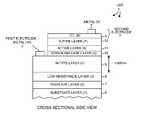
- FIG. 2is a simplified cross-sectional diagram of the blue LED device of FIG. 1 .
- FIG. 3is a table that sets forth the composition, structure, and thickness of each layer of the blue LED device of FIG. 1 and FIG. 2 .
- FIG. 4is a diagram that illustrates an operation of the blue LED device of FIG. 1 and FIG. 2 .
- FIG. 5is a flowchart of a method in accordance with one novel aspect.
- first layerwhen a first layer is referred to as being disposed “over” a second layer, it is to be understood that the first layer can be directly on the second layer, or an intervening layer or layers may be present between the first and second layers.
- the terms such as “over”, “under”, “upper”, “lower”, “top”, “bottom”, “upward”, “downward”, “vertically”, and “laterally”are used herein to describe relative orientations between different parts of the blue LED being described, and it is to be understood that the overall blue LED structure being described can actually be oriented in any way in three-dimensional space.
- FIG. 1is a top-down diagram of a blue Light Emitting Diode (LED) device 1 in accordance with one novel aspect.
- Blue LED device 1includes a first electrode 2 and a second electrode 3 .
- the first electrode 2is a bonding pad of metal.
- the second electrode 3includes a Transparent Conductive Layer (TCL) 4 and a bonding pad of metal 5 .
- TCLTransparent Conductive Layer
- the second electrodecovers more than seventy percent of the surface of the LED device 1 .
- LED device 1is said to be a “laterally contacted” LED device because the bonding pads of both electrodes are disposed on the same side of the LED structure such that they appear laterally oriented with respect to one another in the view of FIG. 1 . Both bonding pads of metal 2 and 5 are accessible from the top of the LED device.
- FIG. 2is a cross-sectional diagram of the LED device 1 of FIG. 1 .
- the bottom layer of LED device 1is a substrate that is substantially transparent to blue light, such as a sapphire substrate 6 (Al 2 O 3 ). This substrate is electrically insulative.
- a template layer 7 of n-doped gallium-nitride (n-GaN)is disposed on the sapphire substrate 6 .
- template layer 7has a thickness of 2000 nm.
- the gallium-nitrideis doped with the n-type dopant silicon to a concentration of 1 ⁇ 10 18 atoms per cubic centimeter.
- the template layer 7is undoped gallium-nitride (u-GaN).
- a Low Resistance Layer (LRL) 8is disposed on template layer 7 .
- LRL 8is called “low resistance” because it has a lower sheet resistance than does an overlying n-type contact layer.
- LRL 8 in the present exampleis a superlattice structure having five periods. Each of the five periods includes a relatively thinner sublayer of aluminum-gallium-nitride (AlGaN) and a relatively thicker sublayer of gallium-nitride (GaN).
- AlGaNaluminum-gallium-nitride
- GaNgallium-nitride
- the aluminum-gallium-nitride sublayeris less than one half the thickness of the gallium-nitride sublayer.
- the relative concentrations of aluminum and gallium in the aluminum-gallium-nitride sublayersis given by Al 0.3 Ga 0.7 N.
- Each thinner aluminum-gallium-nitride sublayer of LRL 8is strained to an adjacent thicker layer of gallium-nitride and/or to an adjacent thicker sublayer of gallium-nitride. In this way, the aluminum-gallium-nitride sublayer is strained to the lattice constant of gallium-nitride.
- the bottom sublayer of the first period that is disposed on and in contact with the underlying gallium-nitride template layer 7is a sublayer of aluminum-gallium-nitride.
- the material of LRL 8is doped with silicon at a concentration of 1 ⁇ 10 18 atoms per cubic centimeter.
- the superlatticeis structured such that regions of so-called electron gas are formed in the gallium-nitride sublayers. As is understood in the art, these electrons have a high mobility. This results in the desired low resistivity of the overall LRL 8 .
- LRL 8 in the present examplehas a sheet resistance that is less than the sheet resistance of an overlying n-type layer.
- n-type layer 9is disposed on LRL 8 .
- This n-type layer 9is an n-doped gallium-nitride layer having a thickness of 2000 nm.
- the gallium-nitrideis doped with the n-type dopant silicon to a concentration of 5 ⁇ 10 18 atoms per cubic centimeter.
- n-type layer 9has a sheet resistance that is about eighteen ohms per square at room temperature (more than fifteen ohms per square).
- the n-type layer 9cannot be too thin or the ability of the underlying LRL superlattice to reduce current crowding will substantially degraded, consequently the n-type layer 9 should be more than 500 nm thick.
- strain release layer 10is disposed on n-type layer 9 .
- strain release layer 10includes thirty periods, where each period includes an indium-gallium-nitride sublayer and a gallium-nitride sublayer.
- the indium-gallium-nitride sublayerhas a thickness of 2 nm and has an indium concentration given by In 0.05 Ga 0.95 N.
- the gallium-nitride sublayerhas a thickness of 2 nm.
- the entire strain release layer 10has a thickness of 120 nm.
- Active layer 11is disposed on strain release layer 10 .
- Active layer 11includes ten periods, where each period includes an indium-gallium-nitride sublayer and a gallium-nitride sublayer.
- the indium-gallium-nitride sublayerhas a thickness of 3 nm.
- the gallium-nitride sublayerhas a thickness of 10 nm.
- Active layer 11has a total thickness of 130 nm.
- P-type layer 12is a single layer of uniformly doped p-type gallium-nitride.
- the upper surface of P-type layer 12has no current focusing ridge structures such as are commonly provided in laser diodes to focus current.
- P-type layer 12has a thickness of 300 nm.
- the gallium-nitrideis uniformly doped throughout with the p-type dopant magnesium to a concentration of 1 ⁇ 10 2 ° atoms per cubic centimeter.
- N-type layer 9 , strain release layer 10 , active layer 11 , and p-type layer 12are referred to together as a PAN structure.
- TCLTransparent Conductive Layer
- ITOindium-tin-oxide
- the metal bonding pad of first electrode 2is a multi-layer metal structure (Ti—Al—Ni—Au) having a thickness of 340 nm.
- Metal bonding pad 5 of the second electrode 3is a multi-layer metal structure (Ni—Au) having a thickness of 220 nm.
- FIG. 3is a table that sets forth the composition, structure and thickness of the constituent layers of the blue LED device 1 of FIG. 1 and FIG. 2 .
- FIG. 4is a cross-sectional diagram that illustrates an operation of blue LED device 1 of FIG. 1 and FIG. 2 .
- LED device 1When current flows from second electrode 3 to first electrode 2 , electrons and holes combine in active layer 11 thereby emitting non-monochromatic light 14 .
- LED device 1is said to be a “blue” LED device in that the light 14 emitted has a wavelength in a range of from approximately 440 nm to approximately 500 nm. Light 14 is emitted in many directions, and some of the light passes through the p-layer 12 on its way out of the LED device.
- current flowshould pass downward through the light generating active layer with a current density that is uniform across the area of the upper surface boundary of the active layer. Once current has passed vertically downward through the active layer, the current is generally concentrated to higher current densities as it turns and flows laterally through the n-type layer to the laterally displaced first electrode. Nevertheless, localized peaks in current density in the n-layer should be minimized. In a real world LED device, however, current crowding may occur such that there is a significantly higher current density in some portions of the active layer than there is in other portions.
- LRL 8serves a first function in reducing current crowding in the overlaying layers and/or in reducing maximum current densities in the overlying layers.
- LRL 8is relatively conductive as compared to overlying n-type layer 9 .
- LRL 8is disposed directly beneath and in contact with n-type layer 9 . Consequently, some current is conducted laterally through LRL 8 as conceptually depicted by arrow 13 in FIG. 4 .
- the sheet resistance of n-type gallium-nitride layer 9is higher than the sheet resistance of LRL 8 , when these sheet resistances are considered at the layer 9 /layer 8 interface.
- the sheet resistance of a layer for this purposecan be measured in various known destructive, nondestructive, direct and indirect ways. In one direct and destructive way, all the LED device layers above the layer of interest are ground away or are otherwise removed. Known chemical mechanical polishing and etching techniques can be employed. The exposed upper surface of the layer of interest is then attached to an insulative substrate, and all the layers below the layer of interest are ground away or otherwise removed. What is left is the layer of interest, isolated from all other layers of the LED device, and mounted to the insulative substrate.
- the sheet resistance of the isolated layeris then measured by probing the exposed upper surface of the layer.
- the sheet resistance of n-type gallium-nitride layer 9 of a thickness of approximately 2000 nmis measured to be more than fifteen ohms per square, whereas the sheet resistance of the underlying LRL 8 is lower than the sheet resistance of layer 9 .
- LRL 8also serves a second function in facilitating the growth of low defect films over a gallium-nitride template grown on a sapphire substrate.
- a gallium-nitride epitaxial layer grown on a sapphire substratehas proven to be a good foundation upon which to fabricate PAN structures of GaN-based LEDs.
- Lattice dislocation densities in gallium-nitride grown on sapphireare typically less than 5 ⁇ 10 8 dislocations per square centimeter. Accordingly, sapphire is commonly considered to be a preferred substrate for blue GaN-based LEDs. Nonetheless, there is still a difference in lattice constants between sapphire and gallium-nitride.
- LRL 8 in LED device 1results in a lower lattice defect density in the overlying epitaxial layers of the blue LED than would otherwise occur.
- the superlattice of LRL 8is not the Al x Ga 1-x N/Al y Ga 1-y N superlattice used in deep UV LEDs where the n-layer of the PAN structure is n-doped AlGaN. Such an Al x Ga 1-x N/Al y Ga 1-y N superlattice if used in a blue LED may actually increase dislocation density.
- n-layer 9is n-doped gallium-nitride that contains substantially no aluminum.
- LRL 8is therefore an AlGaN/GaN superlattice.
- the AlGaN sublayers of the superlatticeare strained to the lattice of thicker layers of gallium-nitride and/or to the lattice of thicker sublayers of gallium-nitride.
- the lattice constant of LRL 8therefore closely matches the lattice constant of underlying gallium-nitride template layer 7 , thereby reducing stress at the interface, and thereby preventing the continued formation of defect threads upward from the template layer 7 .
- the superlattice of LRL 8blocks the threads of dislocations in the template layer 7 from extending upward into the n-type layer 9 .
- Reference numeral 15 in FIG. 4identifies one such dislocation thread. This dislocation thread 15 extends upward from the substrate-to-template interface 16 but it is terminated by LRL 8 .
- the epitaxial layers of the LEDare later grown over LRL 8 , such as n-type layer 9 , the epitaxial layers do not contain a continuation of the same thread 15 .
- FIG. 5is a flowchart of a method 100 .
- a Low Resistance Layer (LRL)is provided (step 101 ) over a sapphire substrate layer.
- the LRLis a superlattice structure having periods. At least one period includes an aluminum-gallium-nitride sublayer and a gallium-nitride sublayer. The aluminum-gallium-nitride sublayers are strained to a gallium-nitride lattice. When considered from its upper surface boundary, the LRL has a sheet resistance that is less than the sheet resistance of an overlying n-type layer. In one example, this LRL is LRL 8 of FIG. 2 and the overlying n-type layer is layer 9 of FIG. 2 .
- An n-type gallium-nitride layeris provided (step 102 ) over and in contact with the LRL.
- This n-type gallium-nitride layeris at least five hundred nanometers thick. When considered from its lower surface boundary, the n-type gallium-nitride layer has a sheet resistance that is greater than fifteen ohms per square. In one example, this n-type gallium-nitride layer is layer 9 of FIG. 2 .
- An active layeris provided (step 103 ) over the n-type gallium-nitride layer.
- the active layeris layer 11 of FIG. 2 that is a multiple quantum well structure involving indium-gallium-nitride sublayers and gallium-nitride sublayers.
- a strain release layeris disposed between the active layer and the underlying n-type gallium-nitride layer. In another example, no intervening strain release layer is present.
- a p-type gallium-nitride layeris provided (step 104 ) over the active layer.
- the p-type gallium-nitride layeris layer 12 of FIG. 2 .
- a first electrodeis provided (step 105 ).
- the first electrodeis disposed on and in electrical contact with at least a portion of the n-type gallium-nitride layer.
- the first electrodeis electrode 2 of FIG. 2 .
- a second electrodeis provided (step 106 ).
- the second electrodeis disposed on and in electrical contact with at least a portion of the p-type gallium-nitride layer.
- the second electrodeis electrode 3 in FIG. 2 .
- a reflective layeris formed to cover the bottom surface of the substrate.
- the steps 101 - 106 of method 100can carried out simultaneously by selling an LED device to another entity, or by otherwise supplying or delivering an LED device to another entity.
- Method 100can also be carried out by performing the steps 101 - 106 sequentially in the manufacture of an LED device.
- An example of the LED deviceis LED device 1 of FIG. 1 and FIG. 2 .
- the LRLcan be fabricated in numerous different suitable ways.
- the LRLinvolves periods, where each period includes a first aluminum-gallium-nitride layer and a second aluminum-gallium-nitride layer, where the aluminum concentrations in the two sublayers differ from one another.
- the composition of the two sublayersis given by Al x Ga 1-x N/Al y Ga 1-y N, where x and y are different nonzero numbers.
- the aluminum-gallium-nitride and gallium-nitride sublayers of the LRLare of different thicknesses, in other examples the sublayers are of substantially the same thickness.
- the aluminum concentration in one of a sublayer containing aluminumcan be graded.
- the LRLcan be an AlInN/GaN superlattice.
- the LRLcan be an AlGaN/AlGaN/GaN superlattice where each period involves three sublayers.
- the substrateneed not be sapphire but rather can be another suitable insulative substrate or another suitable conductive substrate.
- the template layerneed not be n-type gallium-nitride in all examples, but rather can be another suitable template material.
- a template layer of aluminum-nitridemay be used over and in contact with a substrate of silicon.
Landscapes
- Led Devices (AREA)
Abstract
Description
Claims (19)
Priority Applications (6)
| Application Number | Priority Date | Filing Date | Title |
|---|---|---|---|
| US13/178,497US8395165B2 (en) | 2011-07-08 | 2011-07-08 | Laterally contacted blue LED with superlattice current spreading layer |
| CN2012800121838ACN103430331A (en) | 2011-07-08 | 2012-05-23 | Laterally contacted blue LED with superlattice current spreading layer |
| KR1020137023859AKR101543936B1 (en) | 2011-07-08 | 2012-05-23 | Laterally contacted blue led with superlattice current spreading layer |
| JP2014513576AJP5795432B2 (en) | 2011-07-08 | 2012-05-23 | Blue LED with in-plane contact with superlattice current spreading layer |
| PCT/US2012/039208WO2013009394A1 (en) | 2011-07-08 | 2012-05-23 | Laterally contacted blue led with superlattice current spreading layer |
| TW101120378ATW201310698A (en) | 2011-07-08 | 2012-06-07 | Lateral contact blue light emitting diode with superlattice current diffusion layer |
Applications Claiming Priority (1)
| Application Number | Priority Date | Filing Date | Title |
|---|---|---|---|
| US13/178,497US8395165B2 (en) | 2011-07-08 | 2011-07-08 | Laterally contacted blue LED with superlattice current spreading layer |
Publications (2)
| Publication Number | Publication Date |
|---|---|
| US20130009130A1 US20130009130A1 (en) | 2013-01-10 |
| US8395165B2true US8395165B2 (en) | 2013-03-12 |
Family
ID=47438087
Family Applications (1)
| Application Number | Title | Priority Date | Filing Date |
|---|---|---|---|
| US13/178,497Expired - Fee RelatedUS8395165B2 (en) | 2011-07-08 | 2011-07-08 | Laterally contacted blue LED with superlattice current spreading layer |
Country Status (6)
| Country | Link |
|---|---|
| US (1) | US8395165B2 (en) |
| JP (1) | JP5795432B2 (en) |
| KR (1) | KR101543936B1 (en) |
| CN (1) | CN103430331A (en) |
| TW (1) | TW201310698A (en) |
| WO (1) | WO2013009394A1 (en) |
Cited By (2)
| Publication number | Priority date | Publication date | Assignee | Title |
|---|---|---|---|---|
| US20120326120A1 (en)* | 2010-02-05 | 2012-12-27 | Wang-Kyun SHIN | Transparent led wafer module and method for manufacturing same |
| US9299839B2 (en) | 2014-09-01 | 2016-03-29 | United Microelectronics Corporation | PFET and CMOS containing same |
Families Citing this family (12)
| Publication number | Priority date | Publication date | Assignee | Title |
|---|---|---|---|---|
| TWI570911B (en)* | 2014-05-19 | 2017-02-11 | 新世紀光電股份有限公司 | Semiconductor structure |
| KR102224132B1 (en)* | 2014-08-04 | 2021-03-09 | 엘지이노텍 주식회사 | Light emitting device and lighting system |
| KR102164796B1 (en) | 2014-08-28 | 2020-10-14 | 삼성전자주식회사 | Nano-sturucture semiconductor light emitting device |
| CN104332537B (en)* | 2014-10-17 | 2017-06-16 | 厦门乾照光电股份有限公司 | A kind of light emitting diode epitaxial structure of high concentration Te doping |
| CN104332536B (en)* | 2014-10-17 | 2017-02-15 | 厦门乾照光电股份有限公司 | High concentration Te doped light emitting diode epitaxial method |
| CN104810448A (en)* | 2015-03-27 | 2015-07-29 | 中山大学 | Transverse conducting GaN-based luminescent device growing and preparing method |
| CN105576095B (en)* | 2016-03-10 | 2018-02-06 | 厦门市三安光电科技有限公司 | A kind of iii-nitride light emitting devices and preparation method thereof |
| CN109904287B (en)* | 2019-01-29 | 2020-07-31 | 华灿光电(浙江)有限公司 | Light emitting diode epitaxial wafer and growth method thereof |
| US11688825B2 (en)* | 2019-01-31 | 2023-06-27 | Industrial Technology Research Institute | Composite substrate and light-emitting diode |
| TWI859673B (en)* | 2019-05-24 | 2024-10-21 | 晶元光電股份有限公司 | Semiconductor device |
| JP7429522B2 (en)* | 2019-11-22 | 2024-02-08 | 住友化学株式会社 | Group III nitride multilayer substrate and semiconductor device |
| US11322647B2 (en) | 2020-05-01 | 2022-05-03 | Silanna UV Technologies Pte Ltd | Buried contact layer for UV emitting device |
Citations (92)
| Publication number | Priority date | Publication date | Assignee | Title |
|---|---|---|---|---|
| JPH04267376A (en) | 1991-02-22 | 1992-09-22 | Toshiba Corp | Semiconductor light emitting element and fabrication thereof |
| US5306662A (en) | 1991-11-08 | 1994-04-26 | Nichia Chemical Industries, Ltd. | Method of manufacturing P-type compound semiconductor |
| US5408120A (en) | 1992-07-23 | 1995-04-18 | Toyoda Gosei Co., Ltd. | Light-emitting device of gallium nitride compound semiconductor |
| US5432808A (en) | 1993-03-15 | 1995-07-11 | Kabushiki Kaisha Toshiba | Compound semicondutor light-emitting device |
| US5563422A (en) | 1993-04-28 | 1996-10-08 | Nichia Chemical Industries, Ltd. | Gallium nitride-based III-V group compound semiconductor device and method of producing the same |
| JPH08264894A (en) | 1995-03-20 | 1996-10-11 | Toshiba Corp | Semiconductor device and manufacturing method thereof |
| US5578839A (en) | 1992-11-20 | 1996-11-26 | Nichia Chemical Industries, Ltd. | Light-emitting gallium nitride-based compound semiconductor device |
| JP2626431B2 (en) | 1992-10-29 | 1997-07-02 | 豊田合成株式会社 | Nitrogen-3 group element compound semiconductor light emitting device |
| JP2666237B2 (en) | 1994-09-20 | 1997-10-22 | 豊田合成株式会社 | Group III nitride semiconductor light emitting device |
| JP2681733B2 (en) | 1992-10-29 | 1997-11-26 | 豊田合成株式会社 | Nitrogen-3 group element compound semiconductor light emitting device |
| JP2735057B2 (en) | 1994-12-22 | 1998-04-02 | 日亜化学工業株式会社 | Nitride semiconductor light emitting device |
| US5766783A (en) | 1995-03-01 | 1998-06-16 | Sumitomo Electric Industries Ltd. | Boron-aluminum nitride coating and method of producing same |
| US5777350A (en) | 1994-12-02 | 1998-07-07 | Nichia Chemical Industries, Ltd. | Nitride semiconductor light-emitting device |
| JP2778405B2 (en) | 1993-03-12 | 1998-07-23 | 日亜化学工業株式会社 | Gallium nitride based compound semiconductor light emitting device |
| JP2785254B2 (en) | 1993-06-28 | 1998-08-13 | 日亜化学工業株式会社 | Gallium nitride based compound semiconductor light emitting device |
| JP2803741B2 (en) | 1993-03-19 | 1998-09-24 | 日亜化学工業株式会社 | Gallium nitride based compound semiconductor electrode forming method |
| JP2827794B2 (en) | 1993-02-05 | 1998-11-25 | 日亜化学工業株式会社 | Method for growing p-type gallium nitride |
| JPH1140847A (en) | 1997-07-16 | 1999-02-12 | Toshiba Corp | Gallium nitride based semiconductor device and method of manufacturing the same |
| JP2890396B2 (en) | 1995-03-27 | 1999-05-10 | 日亜化学工業株式会社 | Nitride semiconductor light emitting device |
| JP2917742B2 (en) | 1992-07-07 | 1999-07-12 | 日亜化学工業株式会社 | Gallium nitride based compound semiconductor light emitting device and method of manufacturing the same |
| US5959307A (en) | 1995-11-06 | 1999-09-28 | Nichia Chemical Industries Ltd. | Nitride semiconductor device |
| US5959401A (en) | 1996-05-21 | 1999-09-28 | Toyoda Gosei Co., Ltd. | Light-emitting semiconductor device using group III nitride compound |
| JP2956489B2 (en) | 1994-06-24 | 1999-10-04 | 日亜化学工業株式会社 | Crystal growth method of gallium nitride based compound semiconductor |
| US6005258A (en) | 1994-03-22 | 1999-12-21 | Toyoda Gosei Co., Ltd. | Light-emitting semiconductor device using group III Nitrogen compound having emission layer doped with donor and acceptor impurities |
| US6015979A (en)* | 1997-08-29 | 2000-01-18 | Kabushiki Kaisha Toshiba | Nitride-based semiconductor element and method for manufacturing the same |
| US6040588A (en) | 1996-09-08 | 2000-03-21 | Toyoda Gosei Co., Ltd. | Semiconductor light-emitting device |
| JP3063756B1 (en) | 1998-10-06 | 2000-07-12 | 日亜化学工業株式会社 | Nitride semiconductor device |
| JP3063757B1 (en) | 1998-11-17 | 2000-07-12 | 日亜化学工業株式会社 | Nitride semiconductor device |
| US6121635A (en) | 1997-04-15 | 2000-09-19 | Kabushiki Kaisha Toshiba | Semiconductor light-emitting element having transparent electrode and current blocking layer, and semiconductor light-emitting including the same |
| JP3135041B2 (en) | 1995-09-29 | 2001-02-13 | 日亜化学工業株式会社 | Nitride semiconductor light emitting device |
| US6242764B1 (en) | 1997-07-17 | 2001-06-05 | Kabushiki Kaisha Toshiba | III-N semiconductor light-emitting element having strain-moderating crystalline buffer layers |
| JP3223832B2 (en) | 1997-02-24 | 2001-10-29 | 日亜化学工業株式会社 | Nitride semiconductor device and semiconductor laser diode |
| JP3250438B2 (en) | 1995-03-29 | 2002-01-28 | 日亜化学工業株式会社 | Nitride semiconductor light emitting device |
| JP3314666B2 (en) | 1997-06-09 | 2002-08-12 | 日亜化学工業株式会社 | Nitride semiconductor device |
| JP3344257B2 (en) | 1997-01-17 | 2002-11-11 | 豊田合成株式会社 | Gallium nitride based compound semiconductor and device manufacturing method |
| JP3374737B2 (en) | 1997-01-09 | 2003-02-10 | 日亜化学工業株式会社 | Nitride semiconductor device |
| JP3424629B2 (en) | 1998-12-08 | 2003-07-07 | 日亜化学工業株式会社 | Nitride semiconductor device |
| JP3427265B2 (en) | 1998-12-08 | 2003-07-14 | 日亜化学工業株式会社 | Nitride semiconductor device |
| US6617060B2 (en) | 2000-12-14 | 2003-09-09 | Nitronex Corporation | Gallium nitride materials and methods |
| US20030178642A1 (en) | 2002-02-08 | 2003-09-25 | Ngk Insulators, Ltd. | Semiconductor light-emitting devices |
| US6657236B1 (en) | 1999-12-03 | 2003-12-02 | Cree Lighting Company | Enhanced light extraction in LEDs through the use of internal and external optical elements |
| JP3506874B2 (en) | 1997-03-24 | 2004-03-15 | 豊田合成株式会社 | Nitrogen-3 group element compound semiconductor light emitting device |
| JP3511970B2 (en) | 1995-06-15 | 2004-03-29 | 日亜化学工業株式会社 | Nitride semiconductor light emitting device |
| JP3548442B2 (en) | 1994-09-22 | 2004-07-28 | 日亜化学工業株式会社 | Gallium nitride based compound semiconductor light emitting device |
| JP3551101B2 (en) | 1999-03-29 | 2004-08-04 | 日亜化学工業株式会社 | Nitride semiconductor device |
| US6800500B2 (en) | 1999-02-05 | 2004-10-05 | Lumileds Lighting U.S., Llc | III-nitride light emitting devices fabricated by substrate removal |
| US6838693B2 (en) | 2000-07-07 | 2005-01-04 | Nichia Corporation | Nitride semiconductor device |
| US6849881B1 (en) | 1999-11-19 | 2005-02-01 | Osram Gmbh | Optical semiconductor device comprising a multiple quantum well structure |
| JP3622562B2 (en) | 1998-03-12 | 2005-02-23 | 日亜化学工業株式会社 | Nitride semiconductor light emitting diode |
| US6891197B2 (en) | 2001-05-09 | 2005-05-10 | Lumileds Lighting U.S., Llc | Semiconductor LED flip-chip with dielectric coating on the mesa |
| JP3646649B2 (en) | 1994-09-22 | 2005-05-11 | 日亜化学工業株式会社 | Gallium nitride compound semiconductor light emitting device |
| JP3654738B2 (en) | 1997-04-07 | 2005-06-02 | 豊田合成株式会社 | Group 3 nitride semiconductor light emitting device |
| US6906352B2 (en) | 2001-01-16 | 2005-06-14 | Cree, Inc. | Group III nitride LED with undoped cladding layer and multiple quantum well |
| US6916676B2 (en) | 2002-01-28 | 2005-07-12 | Nichia Corporation | Method for producing a nitride semiconductor element |
| US6951695B2 (en) | 2001-06-08 | 2005-10-04 | Cree, Inc. | High surface quality GaN wafer and method of fabricating same |
| US6977395B2 (en) | 2001-07-12 | 2005-12-20 | Nichia Corporation | Semiconductor device |
| JP3748011B2 (en) | 1999-06-11 | 2006-02-22 | 東芝セラミックス株式会社 | Si wafer for GaN semiconductor crystal growth, wafer for GaN light emitting device using the same, and manufacturing method thereof |
| US7026653B2 (en) | 2004-01-27 | 2006-04-11 | Lumileds Lighting, U.S., Llc | Semiconductor light emitting devices including current spreading layers |
| JP3780887B2 (en) | 1996-09-08 | 2006-05-31 | 豊田合成株式会社 | Semiconductor light emitting device and manufacturing method thereof |
| JP3786114B2 (en) | 2000-11-21 | 2006-06-14 | 日亜化学工業株式会社 | Nitride semiconductor device |
| JP3795624B2 (en) | 1997-03-31 | 2006-07-12 | 豊田合成株式会社 | Nitrogen-3 group element compound semiconductor light emitting device |
| US7115908B2 (en) | 2004-01-30 | 2006-10-03 | Philips Lumileds Lighting Company, Llc | III-nitride light emitting device with reduced polarization fields |
| JP3890930B2 (en) | 1995-03-29 | 2007-03-07 | 日亜化学工業株式会社 | Nitride semiconductor light emitting device |
| US7193246B1 (en) | 1998-03-12 | 2007-03-20 | Nichia Corporation | Nitride semiconductor device |
| US7247985B2 (en) | 2003-10-30 | 2007-07-24 | Sharp Kabushiki Kaisha | Semiconductor light-emitting device having annular shape light emitting region and current blocking layer |
| US7262436B2 (en) | 1997-12-15 | 2007-08-28 | Philips Lumileds Lighting Company, Llc | III-nitride semiconductor light emitting device having a silver p-contact |
| US20070210304A1 (en) | 2006-03-10 | 2007-09-13 | Toshiba Ceramics Co., Ltd. | Nitride semiconductor single crystal film |
| US7312474B2 (en) | 2001-05-30 | 2007-12-25 | Cree, Inc. | Group III nitride based superlattice structures |
| US7335920B2 (en) | 2005-01-24 | 2008-02-26 | Cree, Inc. | LED with current confinement structure and surface roughening |
| US7345297B2 (en) | 2004-02-09 | 2008-03-18 | Nichia Corporation | Nitride semiconductor device |
| US7348602B2 (en) | 1999-03-29 | 2008-03-25 | Nichia Corporation | Nitride semiconductor device |
| JP4118370B2 (en) | 1997-12-15 | 2008-07-16 | フィリップス ルミレッズ ライティング カンパニー リミテッド ライアビリティ カンパニー | Nitride semiconductor light-emitting device having reflective p-electrode, method for manufacturing the same, and semiconductor optoelectronic device |
| JP4118371B2 (en) | 1997-12-15 | 2008-07-16 | フィリップス ルミレッズ ライティング カンパニー リミテッド ライアビリティ カンパニー | Nitride semiconductor light emitting device having silver as electrode, method for manufacturing the same, and semiconductor optoelectronic device |
| US7442966B2 (en) | 2002-09-30 | 2008-10-28 | Osram Gmbh | Electromagnetic radiation emitting semiconductor chip and procedure for its production |
| US7446345B2 (en) | 2005-04-29 | 2008-11-04 | Cree, Inc. | Light emitting devices with active layers that extend into opened pits |
| US7547908B2 (en) | 2006-12-22 | 2009-06-16 | Philips Lumilieds Lighting Co, Llc | III-nitride light emitting devices grown on templates to reduce strain |
| US7547925B2 (en) | 2005-11-14 | 2009-06-16 | Palo Alto Research Center Incorporated | Superlattice strain relief layer for semiconductor devices |
| US7691651B2 (en) | 2005-06-10 | 2010-04-06 | Samsung Electro-Mechanics Co., Ltd. | Method for manufacturing nitride-based semiconductor device |
| US7709851B2 (en) | 2004-04-14 | 2010-05-04 | Osram Opto Semiconductors Gmbh | Light-emitting diode chip including a mirror layer and a light-generating active zone |
| US7737459B2 (en) | 2004-09-22 | 2010-06-15 | Cree, Inc. | High output group III nitride light emitting diodes |
| US7754514B2 (en) | 2006-08-22 | 2010-07-13 | Toyoda Gosei Co., Ltd. | Method of making a light emitting element |
| US7791101B2 (en) | 2008-03-28 | 2010-09-07 | Cree, Inc. | Indium gallium nitride-based ohmic contact layers for gallium nitride-based devices |
| US7791061B2 (en) | 2004-05-18 | 2010-09-07 | Cree, Inc. | External extraction light emitting diode based upon crystallographic faceted surfaces |
| US7795623B2 (en) | 2004-06-30 | 2010-09-14 | Cree, Inc. | Light emitting devices having current reducing structures and methods of forming light emitting devices having current reducing structures |
| US7813400B2 (en) | 2006-11-15 | 2010-10-12 | Cree, Inc. | Group-III nitride based laser diode and method for fabricating same |
| JP4629178B2 (en) | 1998-10-06 | 2011-02-09 | 日亜化学工業株式会社 | Nitride semiconductor device |
| US7910945B2 (en) | 2006-06-30 | 2011-03-22 | Cree, Inc. | Nickel tin bonding system with barrier layer for semiconductor wafers and devices |
| US7939844B2 (en) | 2000-05-26 | 2011-05-10 | Osram Gmbh | Light-emitting-diode chip comprising a sequence of GAN-based epitaxial layers which emit radiation and a method for producing the same |
| US7968865B2 (en) | 2006-11-08 | 2011-06-28 | Raytheon Company | Boron aluminum nitride diamond heterostructure |
| US8021904B2 (en) | 2007-02-01 | 2011-09-20 | Cree, Inc. | Ohmic contacts to nitrogen polarity GaN |
| US8030665B2 (en) | 2002-07-08 | 2011-10-04 | Nichia Corporation | Nitride semiconductor device comprising bonded substrate and fabrication method of the same |
| JP4904261B2 (en) | 2004-06-30 | 2012-03-28 | クリー インコーポレイテッド | Light emitting device having current blocking structure and method for manufacturing light emitting device having current blocking structure |
Family Cites Families (9)
| Publication number | Priority date | Publication date | Assignee | Title |
|---|---|---|---|---|
| JP2001077412A (en)* | 1999-09-02 | 2001-03-23 | Sanyo Electric Co Ltd | Semiconductor element and manufacture thereof |
| JP2003077835A (en)* | 2001-09-06 | 2003-03-14 | Ngk Insulators Ltd | Iii nitride element and iii nitride epitaxial substrate |
| CN1431722A (en)* | 2003-02-18 | 2003-07-23 | 华南师范大学 | Blue light emitting device of III group nitrogen semi-conductor |
| JP4604488B2 (en)* | 2003-12-26 | 2011-01-05 | 日亜化学工業株式会社 | Nitride semiconductor light emitting device and manufacturing method thereof |
| KR100580751B1 (en)* | 2004-12-23 | 2006-05-15 | 엘지이노텍 주식회사 | Nitride semiconductor light emitting device and manufacturing method |
| WO2008054994A2 (en)* | 2006-10-18 | 2008-05-08 | Nitek, Inc. | Deep ultraviolet light emitting device and method for fabricating same |
| KR100835116B1 (en)* | 2007-04-16 | 2008-06-05 | 삼성전기주식회사 | Nitride semiconductor light emitting device |
| US8563995B2 (en)* | 2008-03-27 | 2013-10-22 | Nitek, Inc. | Ultraviolet light emitting diode/laser diode with nested superlattice |
| JP4681684B1 (en)* | 2009-08-24 | 2011-05-11 | Dowaエレクトロニクス株式会社 | Nitride semiconductor device and manufacturing method thereof |
- 2011
- 2011-07-08USUS13/178,497patent/US8395165B2/ennot_activeExpired - Fee Related
- 2012
- 2012-05-23WOPCT/US2012/039208patent/WO2013009394A1/enactiveApplication Filing
- 2012-05-23KRKR1020137023859Apatent/KR101543936B1/ennot_activeExpired - Fee Related
- 2012-05-23CNCN2012800121838Apatent/CN103430331A/enactivePending
- 2012-05-23JPJP2014513576Apatent/JP5795432B2/ennot_activeExpired - Fee Related
- 2012-06-07TWTW101120378Apatent/TW201310698A/enunknown
Patent Citations (112)
| Publication number | Priority date | Publication date | Assignee | Title |
|---|---|---|---|---|
| JPH04267376A (en) | 1991-02-22 | 1992-09-22 | Toshiba Corp | Semiconductor light emitting element and fabrication thereof |
| US5468678A (en) | 1991-11-08 | 1995-11-21 | Nichia Chemical Industries, Ltd. | Method of manufacturing P-type compound semiconductor |
| US5306662A (en) | 1991-11-08 | 1994-04-26 | Nichia Chemical Industries, Ltd. | Method of manufacturing P-type compound semiconductor |
| JP2917742B2 (en) | 1992-07-07 | 1999-07-12 | 日亜化学工業株式会社 | Gallium nitride based compound semiconductor light emitting device and method of manufacturing the same |
| USRE36747E (en) | 1992-07-23 | 2000-06-27 | Toyoda Gosei Co., Ltd | Light-emitting device of gallium nitride compound semiconductor |
| US5408120A (en) | 1992-07-23 | 1995-04-18 | Toyoda Gosei Co., Ltd. | Light-emitting device of gallium nitride compound semiconductor |
| JP2626431B2 (en) | 1992-10-29 | 1997-07-02 | 豊田合成株式会社 | Nitrogen-3 group element compound semiconductor light emitting device |
| JP2681733B2 (en) | 1992-10-29 | 1997-11-26 | 豊田合成株式会社 | Nitrogen-3 group element compound semiconductor light emitting device |
| US5734182A (en) | 1992-11-20 | 1998-03-31 | Nichia Chemical Industries Ltd. | Light-emitting gallium nitride-based compound semiconducor device |
| US6215133B1 (en) | 1992-11-20 | 2001-04-10 | Nichia Chemical Industries, Ltd. | Light-emitting gallium nitride-based compound semiconductor device |
| US5578839A (en) | 1992-11-20 | 1996-11-26 | Nichia Chemical Industries, Ltd. | Light-emitting gallium nitride-based compound semiconductor device |
| US5747832A (en) | 1992-11-20 | 1998-05-05 | Nichia Chemical Industries, Ltd. | Light-emitting gallium nitride-based compound semiconductor device |
| JP2827794B2 (en) | 1993-02-05 | 1998-11-25 | 日亜化学工業株式会社 | Method for growing p-type gallium nitride |
| JP2778405B2 (en) | 1993-03-12 | 1998-07-23 | 日亜化学工業株式会社 | Gallium nitride based compound semiconductor light emitting device |
| US5432808A (en) | 1993-03-15 | 1995-07-11 | Kabushiki Kaisha Toshiba | Compound semicondutor light-emitting device |
| JP2803741B2 (en) | 1993-03-19 | 1998-09-24 | 日亜化学工業株式会社 | Gallium nitride based compound semiconductor electrode forming method |
| US5563422A (en) | 1993-04-28 | 1996-10-08 | Nichia Chemical Industries, Ltd. | Gallium nitride-based III-V group compound semiconductor device and method of producing the same |
| US6610995B2 (en) | 1993-04-28 | 2003-08-26 | Nichia Corporation | Gallium nitride-based III-V group compound semiconductor |
| JP2785254B2 (en) | 1993-06-28 | 1998-08-13 | 日亜化学工業株式会社 | Gallium nitride based compound semiconductor light emitting device |
| US6005258A (en) | 1994-03-22 | 1999-12-21 | Toyoda Gosei Co., Ltd. | Light-emitting semiconductor device using group III Nitrogen compound having emission layer doped with donor and acceptor impurities |
| US6265726B1 (en) | 1994-03-22 | 2001-07-24 | Toyoda Gosei Co., Ltd. | Light-emitting aluminum gallium indium nitride compound semiconductor device having an improved luminous intensity |
| US7138286B2 (en) | 1994-03-22 | 2006-11-21 | Toyoda Gosei Co., Ltd. | Light-emitting semiconductor device using group III nitrogen compound |
| JP2956489B2 (en) | 1994-06-24 | 1999-10-04 | 日亜化学工業株式会社 | Crystal growth method of gallium nitride based compound semiconductor |
| JP2666237B2 (en) | 1994-09-20 | 1997-10-22 | 豊田合成株式会社 | Group III nitride semiconductor light emitting device |
| US5753939A (en) | 1994-09-20 | 1998-05-19 | Toyoda Gosei Kk | Light-emitting semiconductor device using a Group III nitride compound and having a contact layer upon which an electrode is formed |
| JP3548442B2 (en) | 1994-09-22 | 2004-07-28 | 日亜化学工業株式会社 | Gallium nitride based compound semiconductor light emitting device |
| JP3646649B2 (en) | 1994-09-22 | 2005-05-11 | 日亜化学工業株式会社 | Gallium nitride compound semiconductor light emitting device |
| US5777350A (en) | 1994-12-02 | 1998-07-07 | Nichia Chemical Industries, Ltd. | Nitride semiconductor light-emitting device |
| JP2735057B2 (en) | 1994-12-22 | 1998-04-02 | 日亜化学工業株式会社 | Nitride semiconductor light emitting device |
| US5766783A (en) | 1995-03-01 | 1998-06-16 | Sumitomo Electric Industries Ltd. | Boron-aluminum nitride coating and method of producing same |
| JPH08264894A (en) | 1995-03-20 | 1996-10-11 | Toshiba Corp | Semiconductor device and manufacturing method thereof |
| JP2890396B2 (en) | 1995-03-27 | 1999-05-10 | 日亜化学工業株式会社 | Nitride semiconductor light emitting device |
| JP3250438B2 (en) | 1995-03-29 | 2002-01-28 | 日亜化学工業株式会社 | Nitride semiconductor light emitting device |
| JP3890930B2 (en) | 1995-03-29 | 2007-03-07 | 日亜化学工業株式会社 | Nitride semiconductor light emitting device |
| JP3511970B2 (en) | 1995-06-15 | 2004-03-29 | 日亜化学工業株式会社 | Nitride semiconductor light emitting device |
| JP3135041B2 (en) | 1995-09-29 | 2001-02-13 | 日亜化学工業株式会社 | Nitride semiconductor light emitting device |
| US5959307A (en) | 1995-11-06 | 1999-09-28 | Nichia Chemical Industries Ltd. | Nitride semiconductor device |
| US5959401A (en) | 1996-05-21 | 1999-09-28 | Toyoda Gosei Co., Ltd. | Light-emitting semiconductor device using group III nitride compound |
| JP3209096B2 (en) | 1996-05-21 | 2001-09-17 | 豊田合成株式会社 | Group III nitride compound semiconductor light emitting device |
| US6040588A (en) | 1996-09-08 | 2000-03-21 | Toyoda Gosei Co., Ltd. | Semiconductor light-emitting device |
| JP3780887B2 (en) | 1996-09-08 | 2006-05-31 | 豊田合成株式会社 | Semiconductor light emitting device and manufacturing method thereof |
| US6420733B2 (en) | 1996-09-08 | 2002-07-16 | Toyoda Gosei Co., Ltd. | Semiconductor light-emitting device and manufacturing method thereof |
| JP3304787B2 (en) | 1996-09-08 | 2002-07-22 | 豊田合成株式会社 | Semiconductor light emitting device and method of manufacturing the same |
| US6326236B1 (en) | 1996-09-08 | 2001-12-04 | Toyoda Gosei Co., Ltd. | Semiconductor light-emitting device and manufacturing method thereof |
| US6541293B2 (en) | 1996-09-08 | 2003-04-01 | Toyoda Gosei Co., Ltd. | Semiconductor light-emitting device and manufacturing method thereof |
| JP3374737B2 (en) | 1997-01-09 | 2003-02-10 | 日亜化学工業株式会社 | Nitride semiconductor device |
| JP3344257B2 (en) | 1997-01-17 | 2002-11-11 | 豊田合成株式会社 | Gallium nitride based compound semiconductor and device manufacturing method |
| JP3223832B2 (en) | 1997-02-24 | 2001-10-29 | 日亜化学工業株式会社 | Nitride semiconductor device and semiconductor laser diode |
| JP3506874B2 (en) | 1997-03-24 | 2004-03-15 | 豊田合成株式会社 | Nitrogen-3 group element compound semiconductor light emitting device |
| JP3795624B2 (en) | 1997-03-31 | 2006-07-12 | 豊田合成株式会社 | Nitrogen-3 group element compound semiconductor light emitting device |
| JP3654738B2 (en) | 1997-04-07 | 2005-06-02 | 豊田合成株式会社 | Group 3 nitride semiconductor light emitting device |
| US6121635A (en) | 1997-04-15 | 2000-09-19 | Kabushiki Kaisha Toshiba | Semiconductor light-emitting element having transparent electrode and current blocking layer, and semiconductor light-emitting including the same |
| JP3314666B2 (en) | 1997-06-09 | 2002-08-12 | 日亜化学工業株式会社 | Nitride semiconductor device |
| JPH1140847A (en) | 1997-07-16 | 1999-02-12 | Toshiba Corp | Gallium nitride based semiconductor device and method of manufacturing the same |
| US6242764B1 (en) | 1997-07-17 | 2001-06-05 | Kabushiki Kaisha Toshiba | III-N semiconductor light-emitting element having strain-moderating crystalline buffer layers |
| US6015979A (en)* | 1997-08-29 | 2000-01-18 | Kabushiki Kaisha Toshiba | Nitride-based semiconductor element and method for manufacturing the same |
| US7262436B2 (en) | 1997-12-15 | 2007-08-28 | Philips Lumileds Lighting Company, Llc | III-nitride semiconductor light emitting device having a silver p-contact |
| JP4118370B2 (en) | 1997-12-15 | 2008-07-16 | フィリップス ルミレッズ ライティング カンパニー リミテッド ライアビリティ カンパニー | Nitride semiconductor light-emitting device having reflective p-electrode, method for manufacturing the same, and semiconductor optoelectronic device |
| JP4118371B2 (en) | 1997-12-15 | 2008-07-16 | フィリップス ルミレッズ ライティング カンパニー リミテッド ライアビリティ カンパニー | Nitride semiconductor light emitting device having silver as electrode, method for manufacturing the same, and semiconductor optoelectronic device |
| JP3622562B2 (en) | 1998-03-12 | 2005-02-23 | 日亜化学工業株式会社 | Nitride semiconductor light emitting diode |
| US7402838B2 (en) | 1998-03-12 | 2008-07-22 | Nichia Corporation | Nitride semiconductor device |
| US7193246B1 (en) | 1998-03-12 | 2007-03-20 | Nichia Corporation | Nitride semiconductor device |
| US7947994B2 (en) | 1998-03-12 | 2011-05-24 | Nichia Corporation | Nitride semiconductor device |
| JP3063756B1 (en) | 1998-10-06 | 2000-07-12 | 日亜化学工業株式会社 | Nitride semiconductor device |
| JP4629178B2 (en) | 1998-10-06 | 2011-02-09 | 日亜化学工業株式会社 | Nitride semiconductor device |
| JP3063757B1 (en) | 1998-11-17 | 2000-07-12 | 日亜化学工業株式会社 | Nitride semiconductor device |
| JP3424629B2 (en) | 1998-12-08 | 2003-07-07 | 日亜化学工業株式会社 | Nitride semiconductor device |
| JP3427265B2 (en) | 1998-12-08 | 2003-07-14 | 日亜化学工業株式会社 | Nitride semiconductor device |
| US7491565B2 (en) | 1999-02-05 | 2009-02-17 | Philips Lumileds Lighting Company, Llc | III-nitride light emitting devices fabricated by substrate removal |
| US6800500B2 (en) | 1999-02-05 | 2004-10-05 | Lumileds Lighting U.S., Llc | III-nitride light emitting devices fabricated by substrate removal |
| JP4860024B2 (en) | 1999-02-05 | 2012-01-25 | フィリップス ルミレッズ ライティング カンパニー リミテッド ライアビリティ カンパニー | InXAlYGaZN light emitting device and manufacturing method thereof |
| JP3551101B2 (en) | 1999-03-29 | 2004-08-04 | 日亜化学工業株式会社 | Nitride semiconductor device |
| US7348602B2 (en) | 1999-03-29 | 2008-03-25 | Nichia Corporation | Nitride semiconductor device |
| JP3748011B2 (en) | 1999-06-11 | 2006-02-22 | 東芝セラミックス株式会社 | Si wafer for GaN semiconductor crystal growth, wafer for GaN light emitting device using the same, and manufacturing method thereof |
| US7106090B2 (en) | 1999-11-19 | 2006-09-12 | Osram Opto Semiconductors Gmbh | Optical semiconductor device with multiple quantum well structure |
| US6849881B1 (en) | 1999-11-19 | 2005-02-01 | Osram Gmbh | Optical semiconductor device comprising a multiple quantum well structure |
| US6657236B1 (en) | 1999-12-03 | 2003-12-02 | Cree Lighting Company | Enhanced light extraction in LEDs through the use of internal and external optical elements |
| US7939844B2 (en) | 2000-05-26 | 2011-05-10 | Osram Gmbh | Light-emitting-diode chip comprising a sequence of GAN-based epitaxial layers which emit radiation and a method for producing the same |
| US6838693B2 (en) | 2000-07-07 | 2005-01-04 | Nichia Corporation | Nitride semiconductor device |
| JP3786114B2 (en) | 2000-11-21 | 2006-06-14 | 日亜化学工業株式会社 | Nitride semiconductor device |
| US6617060B2 (en) | 2000-12-14 | 2003-09-09 | Nitronex Corporation | Gallium nitride materials and methods |
| US6906352B2 (en) | 2001-01-16 | 2005-06-14 | Cree, Inc. | Group III nitride LED with undoped cladding layer and multiple quantum well |
| US6891197B2 (en) | 2001-05-09 | 2005-05-10 | Lumileds Lighting U.S., Llc | Semiconductor LED flip-chip with dielectric coating on the mesa |
| US7312474B2 (en) | 2001-05-30 | 2007-12-25 | Cree, Inc. | Group III nitride based superlattice structures |
| US6951695B2 (en) | 2001-06-08 | 2005-10-04 | Cree, Inc. | High surface quality GaN wafer and method of fabricating same |
| US6977395B2 (en) | 2001-07-12 | 2005-12-20 | Nichia Corporation | Semiconductor device |
| US6916676B2 (en) | 2002-01-28 | 2005-07-12 | Nichia Corporation | Method for producing a nitride semiconductor element |
| US20030178642A1 (en) | 2002-02-08 | 2003-09-25 | Ngk Insulators, Ltd. | Semiconductor light-emitting devices |
| US8030665B2 (en) | 2002-07-08 | 2011-10-04 | Nichia Corporation | Nitride semiconductor device comprising bonded substrate and fabrication method of the same |
| US7442966B2 (en) | 2002-09-30 | 2008-10-28 | Osram Gmbh | Electromagnetic radiation emitting semiconductor chip and procedure for its production |
| US7247985B2 (en) | 2003-10-30 | 2007-07-24 | Sharp Kabushiki Kaisha | Semiconductor light-emitting device having annular shape light emitting region and current blocking layer |
| US7026653B2 (en) | 2004-01-27 | 2006-04-11 | Lumileds Lighting, U.S., Llc | Semiconductor light emitting devices including current spreading layers |
| US7115908B2 (en) | 2004-01-30 | 2006-10-03 | Philips Lumileds Lighting Company, Llc | III-nitride light emitting device with reduced polarization fields |
| US7345297B2 (en) | 2004-02-09 | 2008-03-18 | Nichia Corporation | Nitride semiconductor device |
| US7709851B2 (en) | 2004-04-14 | 2010-05-04 | Osram Opto Semiconductors Gmbh | Light-emitting diode chip including a mirror layer and a light-generating active zone |
| US7791061B2 (en) | 2004-05-18 | 2010-09-07 | Cree, Inc. | External extraction light emitting diode based upon crystallographic faceted surfaces |
| JP4904261B2 (en) | 2004-06-30 | 2012-03-28 | クリー インコーポレイテッド | Light emitting device having current blocking structure and method for manufacturing light emitting device having current blocking structure |
| US7795623B2 (en) | 2004-06-30 | 2010-09-14 | Cree, Inc. | Light emitting devices having current reducing structures and methods of forming light emitting devices having current reducing structures |
| US7737459B2 (en) | 2004-09-22 | 2010-06-15 | Cree, Inc. | High output group III nitride light emitting diodes |
| US7335920B2 (en) | 2005-01-24 | 2008-02-26 | Cree, Inc. | LED with current confinement structure and surface roughening |
| US7446345B2 (en) | 2005-04-29 | 2008-11-04 | Cree, Inc. | Light emitting devices with active layers that extend into opened pits |
| US7611917B2 (en) | 2005-04-29 | 2009-11-03 | Cree, Inc. | Methods of forming light emitting devices with active layers that extend into opened pits |
| US7691651B2 (en) | 2005-06-10 | 2010-04-06 | Samsung Electro-Mechanics Co., Ltd. | Method for manufacturing nitride-based semiconductor device |
| US7547925B2 (en) | 2005-11-14 | 2009-06-16 | Palo Alto Research Center Incorporated | Superlattice strain relief layer for semiconductor devices |
| US20070210304A1 (en) | 2006-03-10 | 2007-09-13 | Toshiba Ceramics Co., Ltd. | Nitride semiconductor single crystal film |
| US7910945B2 (en) | 2006-06-30 | 2011-03-22 | Cree, Inc. | Nickel tin bonding system with barrier layer for semiconductor wafers and devices |
| US7754514B2 (en) | 2006-08-22 | 2010-07-13 | Toyoda Gosei Co., Ltd. | Method of making a light emitting element |
| US7968865B2 (en) | 2006-11-08 | 2011-06-28 | Raytheon Company | Boron aluminum nitride diamond heterostructure |
| US7813400B2 (en) | 2006-11-15 | 2010-10-12 | Cree, Inc. | Group-III nitride based laser diode and method for fabricating same |
| US7547908B2 (en) | 2006-12-22 | 2009-06-16 | Philips Lumilieds Lighting Co, Llc | III-nitride light emitting devices grown on templates to reduce strain |
| US8021904B2 (en) | 2007-02-01 | 2011-09-20 | Cree, Inc. | Ohmic contacts to nitrogen polarity GaN |
| US7791101B2 (en) | 2008-03-28 | 2010-09-07 | Cree, Inc. | Indium gallium nitride-based ohmic contact layers for gallium nitride-based devices |
Non-Patent Citations (4)
| Title |
|---|
| Bae et al., "Surface Investigation of a Cubic AlN Buffer Layer and GaN Grown on Si(111) and Si(100) as Revealed by Atomic Force Microscopy," Journal of the Korean Physical Society, vol. 49, No. 3, Sep. 2006, pp. 1092-1096 (5 pages). |
| Dadgar et al., "Epitaxy of GaN on silicon-impact of symmetry and surface reconstruction," New Journal of Physics, vol. 9, No. 389 (2007); IOP Publishing Ltd., http://iopscience.iop.org/1367-2630/9/10/389 (10 pages). |
| Keyan et al., "Structural analysis of metalorganic chemical vapor deposited AlN nucleation layers on Si(111)," Singapore-MIT Alliance, Jan. 2004, citable URI: http://hdl.handle.net/1721.1/3841 (4 pages). |
| Mike Cooke, "High-Brightness Nitride LEDs on Silicon Through Wafer Bonding", Jun. 4, 2011. (URL: "http://www.semiconductor-today.com/news-items/2011/June/KOREAPHOTONICS-040611.html"). |
Cited By (3)
| Publication number | Priority date | Publication date | Assignee | Title |
|---|---|---|---|---|
| US20120326120A1 (en)* | 2010-02-05 | 2012-12-27 | Wang-Kyun SHIN | Transparent led wafer module and method for manufacturing same |
| US9041045B2 (en)* | 2010-02-05 | 2015-05-26 | Sung-Bok Shin | Transparent LED wafer module and method for manufacturing same |
| US9299839B2 (en) | 2014-09-01 | 2016-03-29 | United Microelectronics Corporation | PFET and CMOS containing same |
Also Published As
| Publication number | Publication date |
|---|---|
| KR101543936B1 (en) | 2015-08-11 |
| KR20130143110A (en) | 2013-12-30 |
| WO2013009394A1 (en) | 2013-01-17 |
| JP2014515564A (en) | 2014-06-30 |
| TW201310698A (en) | 2013-03-01 |
| US20130009130A1 (en) | 2013-01-10 |
| JP5795432B2 (en) | 2015-10-14 |
| CN103430331A (en) | 2013-12-04 |
Similar Documents
| Publication | Publication Date | Title |
|---|---|---|
| US8395165B2 (en) | Laterally contacted blue LED with superlattice current spreading layer | |
| US9012939B2 (en) | N-type gallium-nitride layer having multiple conductive intervening layers | |
| US9159869B2 (en) | LED on silicon substrate using zinc-sulfide as buffer layer | |
| US8865565B2 (en) | LED having a low defect N-type layer that has grown on a silicon substrate | |
| US8686430B2 (en) | Buffer layer for GaN-on-Si LED | |
| US9343641B2 (en) | Non-reactive barrier metal for eutectic bonding process | |
| US9570657B2 (en) | LED that has bounding silicon-doped regions on either side of a strain release layer | |
| CN113571612A (en) | LED epitaxial structure and application thereof, light-emitting diode comprising LED epitaxial structure and preparation method of light-emitting diode | |
| US10388829B2 (en) | Radiation-emitting semiconductor device | |
| HK1191740A (en) | Laterally contacted blue led with superlattice current spreading layer | |
| TWI396306B (en) | Gallium nitride based light emitting diode structure and its making method | |
| Huang et al. | Influence of hydrogen implantation concentration on the characteristics of GaN-based resonant-cavity LEDs | |
| KR20070079139A (en) | Method for manufacturing group III nitride semiconductor laminate and group III nitride semiconductor light emitting device using same | |
| JP2021197532A (en) | Light emitting element | |
| HK1195394A (en) | Non-reactive barrier metal for eutectic bonding process | |
| HK1192797A (en) | N-type gallium-nitride layer having multiple conductive intervening layers |
Legal Events
| Date | Code | Title | Description |
|---|---|---|---|
| AS | Assignment | Owner name:BRIDGELUX, INC., CALIFORNIA Free format text:ASSIGNMENT OF ASSIGNORS INTEREST;ASSIGNORS:CHEN, ZHEN;FENWICK, WILLIAM;LESTER, STEVE;SIGNING DATES FROM 20110630 TO 20110701;REEL/FRAME:026563/0506 | |
| AS | Assignment | Owner name:WHITE OAK GLOBAL ADVISORS, LLC, AS COLLATERAL AGEN Free format text:SECURITY AGREEMENT;ASSIGNOR:BRIDGELUX, INC.;REEL/FRAME:029281/0844 Effective date:20121109 | |
| CC | Certificate of correction | ||
| AS | Assignment | Owner name:BRIDGELUX, INC., CALIFORNIA Free format text:RELEASE BY SECURED PARTY;ASSIGNOR:WHITE OAK GLOBAL ADVISORS, LLC, AS COLLATERAL AGENT;REEL/FRAME:030466/0093 Effective date:20130516 | |
| AS | Assignment | Owner name:TOSHIBA TECHNO CENTER INC., JAPAN Free format text:ASSIGNMENT OF ASSIGNORS INTEREST;ASSIGNOR:BRIDGELUX, INC.;REEL/FRAME:030724/0395 Effective date:20130516 | |
| AS | Assignment | Owner name:KABUSHIKI KAISHA TOSHIBA, JAPAN Free format text:ASSIGNMENT OF ASSIGNORS INTEREST;ASSIGNOR:TOSHIBA TECHNO CENTER INC.;REEL/FRAME:033443/0908 Effective date:20140516 | |
| REMI | Maintenance fee reminder mailed | ||
| LAPS | Lapse for failure to pay maintenance fees | ||
| STCH | Information on status: patent discontinuation | Free format text:PATENT EXPIRED DUE TO NONPAYMENT OF MAINTENANCE FEES UNDER 37 CFR 1.362 | |
| FP | Lapsed due to failure to pay maintenance fee | Effective date:20170312 |