US8394662B1 - Chloride species surface treatment of thin film photovoltaic cell and manufacturing method - Google Patents
Chloride species surface treatment of thin film photovoltaic cell and manufacturing methodDownload PDFInfo
- Publication number
- US8394662B1 US8394662B1US12/564,883US56488309AUS8394662B1US 8394662 B1US8394662 B1US 8394662B1US 56488309 AUS56488309 AUS 56488309AUS 8394662 B1US8394662 B1US 8394662B1
- Authority
- US
- United States
- Prior art keywords
- copper
- indium
- forming
- layer
- species
- Prior art date
- Legal status (The legal status is an assumption and is not a legal conclusion. Google has not performed a legal analysis and makes no representation as to the accuracy of the status listed.)
- Expired - Fee Related, expires
Links
Images


Classifications
- H—ELECTRICITY
- H10—SEMICONDUCTOR DEVICES; ELECTRIC SOLID-STATE DEVICES NOT OTHERWISE PROVIDED FOR
- H10F—INORGANIC SEMICONDUCTOR DEVICES SENSITIVE TO INFRARED RADIATION, LIGHT, ELECTROMAGNETIC RADIATION OF SHORTER WAVELENGTH OR CORPUSCULAR RADIATION
- H10F77/00—Constructional details of devices covered by this subclass
- H10F77/10—Semiconductor bodies
- H10F77/12—Active materials
- H10F77/126—Active materials comprising only Group I-III-VI chalcopyrite materials, e.g. CuInSe2, CuGaSe2 or CuInGaSe2 [CIGS]
- H—ELECTRICITY
- H10—SEMICONDUCTOR DEVICES; ELECTRIC SOLID-STATE DEVICES NOT OTHERWISE PROVIDED FOR
- H10F—INORGANIC SEMICONDUCTOR DEVICES SENSITIVE TO INFRARED RADIATION, LIGHT, ELECTROMAGNETIC RADIATION OF SHORTER WAVELENGTH OR CORPUSCULAR RADIATION
- H10F10/00—Individual photovoltaic cells, e.g. solar cells
- H10F10/10—Individual photovoltaic cells, e.g. solar cells having potential barriers
- H10F10/16—Photovoltaic cells having only PN heterojunction potential barriers
- H10F10/167—Photovoltaic cells having only PN heterojunction potential barriers comprising Group I-III-VI materials, e.g. CdS/CuInSe2 [CIS] heterojunction photovoltaic cells
- Y—GENERAL TAGGING OF NEW TECHNOLOGICAL DEVELOPMENTS; GENERAL TAGGING OF CROSS-SECTIONAL TECHNOLOGIES SPANNING OVER SEVERAL SECTIONS OF THE IPC; TECHNICAL SUBJECTS COVERED BY FORMER USPC CROSS-REFERENCE ART COLLECTIONS [XRACs] AND DIGESTS
- Y02—TECHNOLOGIES OR APPLICATIONS FOR MITIGATION OR ADAPTATION AGAINST CLIMATE CHANGE
- Y02E—REDUCTION OF GREENHOUSE GAS [GHG] EMISSIONS, RELATED TO ENERGY GENERATION, TRANSMISSION OR DISTRIBUTION
- Y02E10/00—Energy generation through renewable energy sources
- Y02E10/50—Photovoltaic [PV] energy
- Y02E10/541—CuInSe2 material PV cells
Definitions
- the present inventionrelates generally to photovoltaic materials and manufacturing method. More particularly, the present invention provides a method and structure for manufacture of high efficiency thin film photovoltaic cells.
- the present method and materialsinclude absorber materials made of copper indium disulfide species, copper tin sulfide, iron disulfide, or others for single junction cells or multi junction cells.
- Petrochemical energyincludes gas and oil.
- Gasincludes lighter forms such as butane and propane, commonly used to heat homes and serve as fuel for cooking.
- Gasalso includes gasoline, diesel, and jet fuel, commonly used for transportation purposes. Heavier forms of petrochemicals can also be used to heat homes in some places.
- the supply of petrochemical fuelis limited and essentially fixed based upon the amount available on the planet Earth. Additionally, as more people use petroleum products in growing amounts, it is rapidly becoming a scarce resource, which will eventually become depleted over time.
- hydroelectric poweris derived from electric generators driven by the flow of water produced by dams such as the Hoover Dam in Nevada. The electric power generated is used to power a large portion of the city of Los Angeles in California. Clean and renewable sources of energy also include wind, waves, biomass, and the like. That is, windmills convert wind energy into more useful forms of energy such as electricity. Still other types of clean energy include solar energy. Specific details of solar energy can be found throughout the present background and more particularly below.
- Solar energy technologygenerally converts electromagnetic radiation from the sun to other useful forms of energy. These other forms of energy include thermal energy and electrical power.
- solar cellsare often used. Although solar energy is environmentally clean and has been successful to a point, many limitations remain to be resolved before it becomes widely used throughout the world.
- one type of solar celluses crystalline materials, which are derived from semiconductor material ingots. These crystalline materials can be used to fabricate optoelectronic devices that include photovoltaic and photodiode devices that convert electromagnetic radiation into electrical power.
- crystalline materialsare often costly and difficult to make on a large scale. Additionally, devices made from such crystalline materials often have low energy conversion efficiencies.
- the present inventionprovides a method and structure for forming semiconductor materials used for the manufacture of high efficiency photovoltaic cells.
- the present method and materialsinclude absorber materials made of copper indium disulfide species, copper tin sulfide, iron disulfide, or others for single junction cells or multi-junction cells.
- a method for forming a thin film photovoltaic deviceincludes providing a transparent substrate comprising a surface region. A first electrode layer is formed overlying the surface region. The method includes forming a copper layer overlying the first electrode layer and forming an indium layer overlying the copper layer to form a multi-layered structure. In a specific embodiment, the method includes subjecting at least the multi-layered structure to a thermal treatment process in an environment containing a sulfur bearing species. The method forms a copper indium disulfide material from at least the thermal treatment process of the multi-layered structure.
- the copper indium disulfide materialcomprising a copper-to-indium atomic ratio ranging from about 1.2:1 to about 2:1 and a thickness of a substantially copper sulfide material having a copper sulfide surface region.
- the methodincludes removing the thickness of the copper sulfide material to expose a surface region having a copper poor surface.
- the copper poor surfacecomprises a copper to indium atomic ratio of less than about 0.95:1.
- the methodsubjects the copper poor surface to a chloride species (for example, derived from cadmium chloride) to convert the copper poor surface from an n-type semiconductor characteristic to a p-type semiconductor characteristic.
- the methodfurther subjects the copper poor surface to a treatment process during a time period associated with the subjecting of the copper poor surface with the chloride species.
- a window layeris formed overlying the copper indium disulfide material.
- a method for forming a thin film photovoltaic deviceincludes providing a transparent substrate comprising a surface region. A first electrode layer is formed overlying the surface region.
- the methodforms a copper indium material comprising an atomic ratio of Cu:In ranging from about 1.35:1 to about 1.60:1 by at least sputtering a target comprising an indium copper material.
- the methodsubjects the copper indium material to a first thermal treatment process in an environment containing a sulfur bearing species to form a copper indium disulfide material from at least the first thermal treatment process of the copper indium material in a specific embodiment.
- a copper poor copper indium disulfide materialis formed within a portion of the copper indium disulfide material.
- the copper poor copper indium disulfide materialhas an atomic ration of Cu:In of about 0.99 and less.
- the methodincludes compensating the copper poor copper indium disulfide material using a chloride species (for example, derived from cadmium chloride) to change in characteristic from an n-type to a p-type. The method further forms a window layer overlying the copper indium disulfide material.
- a method for forming a thin film photovoltaic deviceincludes providing a transparent substrate comprising a surface region. A first electrode layer is formed overlying the surface region The method includes forming a chalcopyrite material overlying the electrode layer.
- the chalcopyrite materialcomprises at least a copper poor copper indium disulfide material.
- the copper poor copper indium disulfide materialincludes a copper poor copper indium disulfide material surface.
- the copper poor copper indium disulfide surfacehas an atomic ratio of Cu:In of about 0.99 and less in a specific embodiment.
- the methodincludes compensating the copper poor copper indium disulfide material using a chloride species (for example, derived from cadmium chloride) to change in the copper poor copper indium disulfide material from an n-type semiconductor characteristic a p-type semiconductor characteristic in a specific embodiment.
- the methodforms a window layer overlying the chalcopyrite material and forms a second electrode layer overlying the window layer.
- a thin film photovoltaic devicein a still yet alternative embodiment, includes a substrate.
- the substrateincludes a surface region.
- a first electrode layeroverlies the surface region.
- a chalcopyrite materialoverlies the first electrode layer.
- the thin film photovoltaic deviceincludes a copper poor copper indium disulfide surface having an atomic ratio of Cu:In of about 0.99 and less.
- the thin film photovoltaic deviceincludes a compensating chloride species (for example, derived from cadmium chloride) provided within one or more portions of the copper poor copper indium disulfide surface to change the copper poor copper indium disulfide surface from an n-type semiconductor characteristic to a p-type semiconductor characteristic in a specific embodiment.
- the semiconductorincludes a window layer overlying the copper indium disulfide material and a second electrode layer overlying the window layer
- the present inventionuses starting materials that are commercially available to form a thin film of semiconductor bearing material overlying a suitable substrate member.
- the thin film of semiconductor bearing materialcan be further processed to form a semiconductor thin film material of desired characteristics, such as atomic stoichiometry, impurity concentration, carrier concentration, doping, and others.
- the band gap of the resulting copper indium disulfide materialis about 1.55 eV.
- the present methoduses environmentally friendly materials that are relatively less toxic than other thin-film photovoltaic materials.
- the present method and resulting structureis substantially free from a parasitic junction on an absorber layer based upon a copper poor chalcopyrite material.
- the open circuit voltage of the chalcopyrite materialsuch as copper indium disulfide ranges from about 0.8 volts and greater and preferably 0.9 volts and greater or 1.0 volts and greater up to 1.2 volts.
- the open circuit voltage of the chalcopyrite materialsuch as copper indium disulfide ranges from about 0.8 volts and greater and preferably 0.9 volts and greater or 1.0 volts and greater up to 1.2 volts.
- the open circuit voltage of the chalcopyrite materialsuch as copper indium disulfide ranges from about 0.8 volts and greater and preferably 0.9 volts and greater or 1.0 volts and greater up to 1.2 volts.
- the present method and materialsinclude absorber materials made of copper indium disulfide species, copper tin sulfide, iron disulfide, or others for single junction cells or multi junction cells.
- the present inventionprovides a method for manufacturing thin film photovoltaic devices.
- the methodhas been used to provide a copper indium disulfide thin film material for high efficiency solar cell application.
- the present inventionhas a much broader range of applicability, for example, embodiments of the present invention may be used to form other semiconducting thin films or multilayers comprising iron sulfide, cadmium sulfide, zinc selenide, and others, and metal oxides such as zinc oxide, iron oxide, copper oxide, and others.
- FIGS. 1-8are simplified schematic diagrams illustrating a method for forming a thin film photovoltaic device according to an embodiment of the present invention. These diagrams are merely examples, which should not unduly limit the claims herein. One skilled in the art would recognize other variations, modifications, and alternatives.
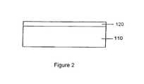
- a substrate 110is provided.
- the substrate 110includes a surface region 112 and is held in a process stage within a process chamber (not shown).
- the substrate 110is an optically transparent solid material.
- substrate 110can use material such as glass, quartz, fused silica, or plastic, or metal, or foil, or semiconductor, or composite materials.
- the substratecan be a single material, multiple materials, which are layered, composites, or stacked, including combinations of these, and the like. Of course there can be other variations, modifications, and alternatives.
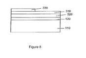
- the present methodforms an electrode layer 120 overlying a surface region 112 of substrate 110 .
- the electrode layercan be a suitable metal material, a semiconductor material or a transparent conducting oxide material, or a combination.
- Electrode layer 120can be formed using techniques such as sputtering, evaporation (e.g., using electron beam), electro-plating, or a combination of these, and the like, according to a specific embodiment.
- the electrode layeris characterized by a resistivity of about 10 Ohm/cm 2 to 100 Ohm/cm 2 and less according to a specific embodiment.
- the electrode layercan be made of molybdenum or tungsten.
- the electrode layercan have a thickness ranging from about 100 nm to 2 micron in a specific embodiment, but can also be others depending on the application.
- Other suitable materialssuch as copper, chromium, aluminum, nickel, or platinum, and the like may also be used.
- copper, chromium, aluminum, nickel, or platinum, and the likemay also be used.
- the atomic ratio Cu:Inis provided such that Cu is limiting, which consumes essentially all of the indium species provided for the resulting structure.
- indium layer 140is provided to cause substantially no change in the copper layer 130 formed until further processing.
- indium layer 140can be first deposited overlying the electrode layer followed by deposition of the copper layer 130 overlying the indium layer.
- multilayered structure 150is subjected to a thermal treatment process 200 .
- the thermal treatment processis provided in an environment containing at least a sulfur bearing species 210 .
- the thermal treatment processis performed at an adequate pressure and temperature.
- the thermal treatment processis provided at a temperature ranging from about 400 Degrees Celsius to about 600 Degrees Celsius.
- the thermal treatment processcan be a rapid thermal process provided at the temperature range for about three to fifteen minutes.
- the sulfur bearing speciesis in a fluid phase.
- the sulfur bearing speciescan be provided in a solution, which has dissolved Na 2 S, CS 2 , (NH 4 ) 2 S, thiosulfate, among others.
- the sulfur bearing speciescan be provided as a layer material overlying the indium and copper layers or copper and indium layers. In a specific embodiment, the sulfur bearing species is provided as a thin layer or as a patterned layer. Depending upon the embodiment, the sulfur bearing species can be provided as a slurry, a powder, a solid material, a gas, a paste, or other suitable form. Of course, there can be other variations, modifications, and alternatives.
- the thermal treatment process 200causes a reaction between copper indium material within the multilayered structure 150 and the sulfur bearing species 210 , thereby forming a layer of copper indium disulfide material (or a copper indium disulfide thin film) 220 .
- the copper indium disulfide material or copper indium disulfide thin film 220is formed by incorporating sulfur ions/atoms stripped or decomposed from the sulfur bearing species into the multilayered structure 150 with indium atoms and copper atoms mutually diffused therein.
- the thermal treatment process 200results in a formation of a cap layer 221 overlying the transformed copper indium disulfide material 220 .
- the solution of potassium cyanideacts as an etchant that is capable of selectively removing copper sulfide material 221 from the surface region of the copper indium disulfide material.
- the etching processstarts from the exposed surface region 225 and down to the thickness of the copper sulfide material 221 and substantially stopped at the interface between the copper sulfide material 221 and copper indium disulfide material 220 .
- the copper sulfide cap layer 221is selectively removed by the etching process to expose surface region 228 of the copper indium disulfide thin film material according to a specific embodiment.
- the etch selectivityis about 1:100 or more between copper sulfide and copper indium disulfide material.
- etching speciescan be hydrogen peroxide.
- other techniquesincluding electro-chemical etching, plasma etching, sputter-etching, or any combination of these may be used.
- the copper sulfide materialcan be mechanically removed, chemically removed, electrically removed, or any combination of these, and others.
- an absorber layer made of copper indium disulfidecan have a thickness of about 1 to 10 microns, but can be others. Of course, there can be other variations, modifications, and alternatives.
- a window layer 310is formed overlying the p-type copper indium disulfide material 320 .
- the window layercan be selected from a group consisting of a cadmium sulfide (CdS), a zinc sulfide (ZnS), zinc selenium (ZnSe), zinc oxide (ZnO), zinc magnesium oxide (ZnMgO), or others. In certain embodiments, these materials may be doped with one or more suitable impurities to form an n + type semiconductor material.
- the window layer and the absorber layerforms a PN junction associated with a photovoltaic cell.
- the window layeris heavily doped to form a n + -type semiconductor layer in a preferred embodiment.
- a transparent substratecomprising a surface region
- the present inventionprovides a method and resulting photovoltaic structure free from parasitic junction regions in the absorber layer, which impair performance of the resulting device.
- Other alternativescan also be provided where steps are added, one or more steps are removed, or one or more steps are provided in a different sequence without departing from the scope of the claims herein. Details of the present method and structure can be found throughout the present specification and more particularly below.
- FIGS. 9-11are simplified diagrams illustrating a method and structure for forming a thin film photovoltaic device including sodium species treatment according to an embodiment of the present invention. These diagrams are merely examples, which should not unduly limit the scope of the claims herein. One of ordinary skill in the art would recognize other variations, modifications, and alternatives.
- the present methodbegins with partially completed photovoltaic device 900 .
- the deviceincludes a transparent substrate 901 comprising a surface region, although other substrates can be used.
- the devicealso includes a first electrode layer 903 overlying the surface region.
- the first electrode layercan be any conductive material including conductive metals, oxides, and semiconductor or combinations of these, as well as any material described herein and outside of the present specification.
- the photovoltaic deviceincludes a chalcopyrite material, which acts as an absorber for the photovoltaic device.
- the chalcopyrite materialcan include, among others, copper indium disulfide material, copper indium aluminum disulfide, copper indium gallium disulfide, combinations of these, and others.
- the chalcopyritehas a thin layer of copper sulfide 907 , which has been previously described, as may remain as a residue or fixed material.
- copper sulfide 907which has been previously described, as may remain as a residue or fixed material.
- the methodselectively removes the thin layer of copper sulfide.
- the thin layeris removed 909 using a solution of potassium cyanide (KCN) or other suitable technique, e.g., dry etching, plasma etching, sputtering.
- KCNpotassium cyanide
- the methodmay cause formation of a copper poor surface region 1001 .
- the copper poor surfaceis characterized by a copper to indium atomic ratio of less than about 0.95:1 or 0.99:1.
- the copper poor surface regionis characterized as an n-type material, which forms a parasitic junction with the p-type copper indium disulfide material, which can be rich in copper. The parasitic junction leads to poor or inefficient device performance.
- the ionic speciescan be applied using one or more techniques. These techniques include deposition, sputtering, spin coating, spraying, spray pyrolysis, dipping, electro deposition, painting, ink jet coating, sprinkling, any combination of these, and others.
- the ionic speciescan be diffused from an overlying material, which can be an electrode layer or molybdenum or other suitable material.
- the ionic speciescan be diffused from a piece of, for example, cadmium chloride material or the like via a vapor phase.
- the ionic species derived from cadmium chloridecan be diffused in vapor phase, but can be others, for short periods of time.
- the treatment processpassivates the surface at the heterojunction or the like, which facilitates carrier separation and transport. Additionally, the present treatment process can also generate desired conduction band offset, commonly called CBO. Of course, there can be other variations, modifications, and alternatives.
Landscapes
- Photovoltaic Devices (AREA)
Abstract
Description
Claims (26)
Priority Applications (1)
| Application Number | Priority Date | Filing Date | Title |
|---|---|---|---|
| US12/564,883US8394662B1 (en) | 2008-09-29 | 2009-09-22 | Chloride species surface treatment of thin film photovoltaic cell and manufacturing method |
Applications Claiming Priority (2)
| Application Number | Priority Date | Filing Date | Title |
|---|---|---|---|
| US10111008P | 2008-09-29 | 2008-09-29 | |
| US12/564,883US8394662B1 (en) | 2008-09-29 | 2009-09-22 | Chloride species surface treatment of thin film photovoltaic cell and manufacturing method |
Publications (1)
| Publication Number | Publication Date |
|---|---|
| US8394662B1true US8394662B1 (en) | 2013-03-12 |
Family
ID=47780424
Family Applications (1)
| Application Number | Title | Priority Date | Filing Date |
|---|---|---|---|
| US12/564,883Expired - Fee RelatedUS8394662B1 (en) | 2008-09-29 | 2009-09-22 | Chloride species surface treatment of thin film photovoltaic cell and manufacturing method |
Country Status (1)
| Country | Link |
|---|---|
| US (1) | US8394662B1 (en) |
Cited By (2)
| Publication number | Priority date | Publication date | Assignee | Title |
|---|---|---|---|---|
| US20120264255A1 (en)* | 2009-10-07 | 2012-10-18 | Nexcis | Production of thin films having photovoltaic properties and containing a i-iii-vi2-type alloy, comprising successive electrodeposits and thermal post-treatment |
| US20130078757A1 (en)* | 2011-09-26 | 2013-03-28 | General Electric Company | Methods of making photovoltaic devices |
Citations (203)
| Publication number | Priority date | Publication date | Assignee | Title |
|---|---|---|---|---|
| US3520732A (en) | 1965-10-22 | 1970-07-14 | Matsushita Electric Industrial Co Ltd | Photovoltaic cell and process of preparation of same |
| US3975211A (en) | 1975-03-28 | 1976-08-17 | Westinghouse Electric Corporation | Solar cells and method for making same |
| US4062038A (en) | 1976-01-28 | 1977-12-06 | International Business Machines Corporation | Radiation responsive device |
| US4332974A (en) | 1979-06-28 | 1982-06-01 | Chevron Research Company | Multilayer photovoltaic cell |
| US4335266A (en) | 1980-12-31 | 1982-06-15 | The Boeing Company | Methods for forming thin-film heterojunction solar cells from I-III-VI.sub.2 |
| DE3314197A1 (en) | 1982-04-28 | 1983-11-03 | Energy Conversion Devices, Inc., 48084 Troy, Mich. | P-CONDUCTING AMORPHOUS SILICON ALLOY WITH A LARGE BAND GAP AND MANUFACTURING PROCESS THEREFOR |
| US4441113A (en) | 1981-02-13 | 1984-04-03 | Energy Conversion Devices, Inc. | P-Type semiconductor material having a wide band gap |
| US4442310A (en) | 1982-07-15 | 1984-04-10 | Rca Corporation | Photodetector having enhanced back reflection |
| US4461922A (en) | 1983-02-14 | 1984-07-24 | Atlantic Richfield Company | Solar cell module |
| US4465575A (en) | 1981-09-21 | 1984-08-14 | Atlantic Richfield Company | Method for forming photovoltaic cells employing multinary semiconductor films |
| US4471155A (en) | 1983-04-15 | 1984-09-11 | Energy Conversion Devices, Inc. | Narrow band gap photovoltaic devices with enhanced open circuit voltage |
| US4499658A (en) | 1983-09-06 | 1985-02-19 | Atlantic Richfield Company | Solar cell laminates |
| US4507181A (en) | 1984-02-17 | 1985-03-26 | Energy Conversion Devices, Inc. | Method of electro-coating a semiconductor device |
| US4517403A (en) | 1983-05-16 | 1985-05-14 | Atlantic Richfield Company | Series connected solar cells and method of formation |
| US4518855A (en) | 1982-09-30 | 1985-05-21 | Spring-Mornne, Inc. | Method and apparatus for statically aligning shafts and monitoring shaft alignment |
| US4532372A (en) | 1983-12-23 | 1985-07-30 | Energy Conversion Devices, Inc. | Barrier layer for photovoltaic devices |
| US4542255A (en) | 1984-01-03 | 1985-09-17 | Atlantic Richfield Company | Gridded thin film solar cell |
| US4581108A (en) | 1984-01-06 | 1986-04-08 | Atlantic Richfield Company | Process of forming a compound semiconductive material |
| US4589194A (en) | 1983-12-29 | 1986-05-20 | Atlantic Richfield Company | Ultrasonic scribing of thin film solar cells |
| US4598306A (en) | 1983-07-28 | 1986-07-01 | Energy Conversion Devices, Inc. | Barrier layer for photovoltaic devices |
| US4599154A (en) | 1985-03-15 | 1986-07-08 | Atlantic Richfield Company | Electrically enhanced liquid jet processing |
| US4611091A (en) | 1984-12-06 | 1986-09-09 | Atlantic Richfield Company | CuInSe2 thin film solar cell with thin CdS and transparent window layer |
| US4623601A (en) | 1985-06-04 | 1986-11-18 | Atlantic Richfield Company | Photoconductive device containing zinc oxide transparent conductive layer |
| US4625070A (en) | 1985-08-30 | 1986-11-25 | Atlantic Richfield Company | Laminated thin film solar module |
| US4638111A (en) | 1985-06-04 | 1987-01-20 | Atlantic Richfield Company | Thin film solar cell module |
| US4661370A (en) | 1984-02-08 | 1987-04-28 | Atlantic Richfield Company | Electric discharge processing of thin films |
| US4663495A (en) | 1985-06-04 | 1987-05-05 | Atlantic Richfield Company | Transparent photovoltaic module |
| US4724011A (en) | 1983-05-16 | 1988-02-09 | Atlantic Richfield Company | Solar cell interconnection by discrete conductive regions |
| US4727047A (en) | 1980-04-10 | 1988-02-23 | Massachusetts Institute Of Technology | Method of producing sheets of crystalline material |
| US4751149A (en) | 1985-06-04 | 1988-06-14 | Atlantic Richfield Company | Chemical vapor deposition of zinc oxide films and products |
| US4775425A (en) | 1987-07-27 | 1988-10-04 | Energy Conversion Devices, Inc. | P and n-type microcrystalline semiconductor alloy material including band gap widening elements, devices utilizing same |
| US4798660A (en) | 1985-07-16 | 1989-01-17 | Atlantic Richfield Company | Method for forming Cu In Se2 films |
| US4816082A (en) | 1987-08-19 | 1989-03-28 | Energy Conversion Devices, Inc. | Thin film solar cell including a spatially modulated intrinsic layer |
| US4873118A (en) | 1988-11-18 | 1989-10-10 | Atlantic Richfield Company | Oxygen glow treating of ZnO electrode for thin film silicon solar cell |
| US4915745A (en) | 1988-09-22 | 1990-04-10 | Atlantic Richfield Company | Thin film solar cell and method of making |
| US4950615A (en) | 1989-02-06 | 1990-08-21 | International Solar Electric Technology, Inc. | Method and making group IIB metal - telluride films and solar cells |
| US4968354A (en) | 1987-11-09 | 1990-11-06 | Fuji Electric Co., Ltd. | Thin film solar cell array |
| US4996108A (en) | 1989-01-17 | 1991-02-26 | Simon Fraser University | Sheets of transition metal dichalcogenides |
| US5008062A (en) | 1988-01-20 | 1991-04-16 | Siemens Solar Industries, L.P. | Method of fabricating photovoltaic module |
| US5011565A (en) | 1989-12-06 | 1991-04-30 | Mobil Solar Energy Corporation | Dotted contact solar cell and method of making same |
| US5028274A (en) | 1989-06-07 | 1991-07-02 | International Solar Electric Technology, Inc. | Group I-III-VI2 semiconductor films for solar cell application |
| US5039353A (en) | 1989-04-27 | 1991-08-13 | Societe Dite: Solems (Societe Anonyme) | Process for improving the spectral response of a photoconductive structure, and improved solar cell and photoreceptive structure |
| US5045409A (en) | 1987-11-27 | 1991-09-03 | Atlantic Richfield Company | Process for making thin film solar cell |
| US5078803A (en) | 1989-09-22 | 1992-01-07 | Siemens Solar Industries L.P. | Solar cells incorporating transparent electrodes comprising hazy zinc oxide |
| US5125984A (en) | 1990-05-31 | 1992-06-30 | Siemens Aktiengesellschaft | Induced junction chalcopyrite solar cell |
| US5133809A (en) | 1989-10-07 | 1992-07-28 | Showa Shell Sekiyu K.K. | Photovoltaic device and process for manufacturing the same |
| US5137835A (en) | 1990-07-24 | 1992-08-11 | Siemens Aktiengesellschaft | Method for manufacturing a chalcopyrite solar cell |
| US5154777A (en) | 1990-02-26 | 1992-10-13 | Mcdonnell Douglas Corporation | Advanced survivable space solar power system |
| US5180686A (en) | 1988-10-31 | 1993-01-19 | Energy Conversion Devices, Inc. | Method for continuously deposting a transparent oxide material by chemical pyrolysis |
| US5211824A (en) | 1991-10-31 | 1993-05-18 | Siemens Solar Industries L.P. | Method and apparatus for sputtering of a liquid |
| US5217564A (en) | 1980-04-10 | 1993-06-08 | Massachusetts Institute Of Technology | Method of producing sheets of crystalline material and devices made therefrom |
| US5231047A (en) | 1991-12-19 | 1993-07-27 | Energy Conversion Devices, Inc. | High quality photovoltaic semiconductor material and laser ablation method of fabrication same |
| US5248345A (en) | 1990-10-17 | 1993-09-28 | Showa Shell Sekiyu K.K. | Integrated photovoltaic device |
| US5261968A (en) | 1992-01-13 | 1993-11-16 | Photon Energy, Inc. | Photovoltaic cell and method |
| US5298086A (en) | 1992-05-15 | 1994-03-29 | United Solar Systems Corporation | Method for the manufacture of improved efficiency tandem photovoltaic device and device manufactured thereby |
| US5336623A (en) | 1992-03-02 | 1994-08-09 | Showa Shell Sekiyu K.K. | Process for producing integrated solar cell |
| US5346853A (en) | 1992-06-29 | 1994-09-13 | United Solar Systems Corporation | Microwave energized deposition process with substrate temperature control for the fabrication of P-I-N photovoltaic devices |
| US5397401A (en) | 1992-06-29 | 1995-03-14 | Canon Kabushiki Kaisha | Semiconductor apparatus covered with a sealing resin composition |
| US5445847A (en) | 1992-05-19 | 1995-08-29 | Matsushita Electric Industrial Co., Ltd. | Method for preparing chalcopyrite-type compound |
| US5474939A (en) | 1992-12-30 | 1995-12-12 | Siemens Solar Industries International | Method of making thin film heterojunction solar cell |
| US5501744A (en) | 1992-01-13 | 1996-03-26 | Photon Energy, Inc. | Photovoltaic cell having a p-type polycrystalline layer with large crystals |
| US5512107A (en) | 1992-03-19 | 1996-04-30 | Siemens Solar Gmbh | Environmentally stable thin-film solar module |
| US5528397A (en) | 1991-12-03 | 1996-06-18 | Kopin Corporation | Single crystal silicon transistors for display panels |
| US5536333A (en) | 1992-05-12 | 1996-07-16 | Solar Cells, Inc. | Process for making photovoltaic devices and resultant product |
| US5578503A (en) | 1992-09-22 | 1996-11-26 | Siemens Aktiengesellschaft | Rapid process for producing a chalcopyrite semiconductor on a substrate |
| US5578103A (en) | 1994-08-17 | 1996-11-26 | Corning Incorporated | Alkali metal ion migration control |
| US5622634A (en) | 1993-12-17 | 1997-04-22 | Canon Kabushiki Kaisha | Method of manufacturing electron-emitting device, electron source and image-forming apparatus |
| US5626688A (en) | 1994-12-01 | 1997-05-06 | Siemens Aktiengesellschaft | Solar cell with chalcopyrite absorber layer |
| US5665175A (en) | 1990-05-30 | 1997-09-09 | Safir; Yakov | Bifacial solar cell |
| US5676766A (en) | 1993-09-30 | 1997-10-14 | Siemens Aktiengesellschaft | Solar cell having a chalcopyrite absorber layer |
| US5726065A (en) | 1995-02-21 | 1998-03-10 | Imec Vzw | Method of preparing solar cell front contacts |
| US5738731A (en) | 1993-11-19 | 1998-04-14 | Mega Chips Corporation | Photovoltaic device |
| US5868869A (en) | 1995-06-07 | 1999-02-09 | Photon Energy, Inc. | Thin film photovoltaic device and process of manufacture |
| US5977476A (en) | 1996-10-16 | 1999-11-02 | United Solar Systems Corporation | High efficiency photovoltaic device |
| US5981868A (en) | 1996-10-25 | 1999-11-09 | Showa Shell Sekiyu K.K. | Thin-film solar cell comprising thin-film light absorbing layer of chalcopyrite multi-element compound semiconductor |
| US5985691A (en) | 1997-05-16 | 1999-11-16 | International Solar Electric Technology, Inc. | Method of making compound semiconductor films and making related electronic devices |
| US6040521A (en) | 1996-11-08 | 2000-03-21 | Showa Shell Sekiyu K.K. | N-type window layer for a thin film solar cell and method of making |
| US6048442A (en) | 1996-10-25 | 2000-04-11 | Showa Shell Sekiyu K.K. | Method for producing thin-film solar cell and equipment for producing the same |
| JP2000173969A (en) | 1998-12-03 | 2000-06-23 | Canon Inc | Rinse method and photovoltaic device |
| JP2000219512A (en) | 1998-11-24 | 2000-08-08 | Canon Inc | Method for manufacturing zinc oxide thin film, method for manufacturing photovoltaic device using the same, and photovoltaic device |
| US6107562A (en) | 1998-03-24 | 2000-08-22 | Matsushita Electric Industrial Co., Ltd. | Semiconductor thin film, method for manufacturing the same, and solar cell using the same |
| US6127202A (en) | 1998-07-02 | 2000-10-03 | International Solar Electronic Technology, Inc. | Oxide-based method of making compound semiconductor films and making related electronic devices |
| US6166319A (en) | 1997-08-01 | 2000-12-26 | Canon Kabushiki Kaisha | Multi-junction photovoltaic device with microcrystalline I-layer |
| US6172297B1 (en) | 1997-09-23 | 2001-01-09 | Institut Fur Solarenergieforschung Gmbh | Solar cell and method for fabrication of a solar cell |
| US6258620B1 (en) | 1997-10-15 | 2001-07-10 | University Of South Florida | Method of manufacturing CIGS photovoltaic devices |
| WO2001057932A1 (en) | 2000-02-07 | 2001-08-09 | Cis Solartechnik Gmbh | Flexible metal substrate for cis solar cells, and method for producing the same |
| US6294274B1 (en) | 1998-11-16 | 2001-09-25 | Tdk Corporation | Oxide thin film |
| US6307148B1 (en)* | 1999-03-29 | 2001-10-23 | Shinko Electric Industries Co., Ltd. | Compound semiconductor solar cell and production method thereof |
| US6328871B1 (en) | 1999-08-16 | 2001-12-11 | Applied Materials, Inc. | Barrier layer for electroplating processes |
| US20020002992A1 (en) | 1998-06-30 | 2002-01-10 | Toshimitsu Kariya | Photovoltaic element |
| US20020004302A1 (en) | 1995-09-14 | 2002-01-10 | Yoshihiko Fukumoto | Method for fabricating semiconductor device |
| US6361718B1 (en) | 1998-02-05 | 2002-03-26 | Nippon Sheet Glass Co., Ltd. | Article having uneven surface, production process for the article, and composition for the process |
| US6372538B1 (en) | 2000-03-16 | 2002-04-16 | University Of Delaware | Fabrication of thin-film, flexible photovoltaic module |
| US20020061361A1 (en) | 2000-09-06 | 2002-05-23 | Hiroki Nakahara | Method and apparatus for fabricating electro-optical device and method and apparatus for fabricating liquid crystal panel |
| US20020063065A1 (en) | 2000-09-19 | 2002-05-30 | Yuichi Sonoda | Method of forming zinc oxide film and process for producing photovoltaic device using it |
| JP2002167695A (en) | 2000-09-19 | 2002-06-11 | Canon Inc | Method for forming zinc oxide film and method for manufacturing photovoltaic element using the same |
| US6423565B1 (en) | 2000-05-30 | 2002-07-23 | Kurt L. Barth | Apparatus and processes for the massproduction of photovotaic modules |
| DE10104726A1 (en) | 2001-02-02 | 2002-08-08 | Siemens Solar Gmbh | Process for structuring an oxide layer applied to a carrier material |
| JP2002270871A (en) | 2001-03-12 | 2002-09-20 | Canon Inc | Semiconductor element and method of forming silicon-based thin film |
| JP2002299670A (en) | 2001-04-03 | 2002-10-11 | Canon Inc | Silicon based thin film and photovoltaic device |
| US20030075717A1 (en) | 2001-03-12 | 2003-04-24 | Takaharu Kondo | Semiconductor element, and method of forming silicon-based film |
| US20030089899A1 (en) | 2000-08-22 | 2003-05-15 | Lieber Charles M. | Nanoscale wires and related devices |
| US6632113B1 (en) | 1998-09-09 | 2003-10-14 | Canon Kabushiki Kaisha | Image display apparatus, disassembly processing method therefor, and component recovery method |
| US6635307B2 (en) | 2001-12-12 | 2003-10-21 | Nanotek Instruments, Inc. | Manufacturing method for thin-film solar cells |
| US6653701B1 (en) | 1999-03-09 | 2003-11-25 | Fuji Xerox Co., Ltd. | Semiconductor device and production method thereof |
| US6667492B1 (en) | 1997-11-10 | 2003-12-23 | Don L. Kendall | Quantum ridges and tips |
| US6690041B2 (en) | 2002-05-14 | 2004-02-10 | Global Solar Energy, Inc. | Monolithically integrated diodes in thin-film photovoltaic devices |
| US20040063320A1 (en) | 2002-09-30 | 2004-04-01 | Hollars Dennis R. | Manufacturing apparatus and method for large-scale production of thin-film solar cells |
| US20040084080A1 (en) | 2002-06-22 | 2004-05-06 | Nanosolar, Inc. | Optoelectronic device and fabrication method |
| US20040095658A1 (en) | 2002-09-05 | 2004-05-20 | Nanosys, Inc. | Nanocomposites |
| US6784492B1 (en) | 1991-03-18 | 2004-08-31 | Canon Kabushiki Kaisha | Semiconductor device including a gate-insulated transistor |
| US20040187917A1 (en) | 2003-03-29 | 2004-09-30 | Nanosolar, Inc. | Transparent electrode, optoelectronic apparatus and devices |
| JP2004332043A (en) | 2003-05-07 | 2004-11-25 | Canon Inc | Method and apparatus for forming zinc oxide thin film, and method for forming photovoltaic element |
| US20040245912A1 (en) | 2003-04-01 | 2004-12-09 | Innovalight | Phosphor materials and illumination devices made therefrom |
| US20040252488A1 (en) | 2003-04-01 | 2004-12-16 | Innovalight | Light-emitting ceiling tile |
| US20040256001A1 (en) | 2002-12-17 | 2004-12-23 | General Electric Company | Photovoltaic cell using stable cu2o nanocrystals and conductive polymers |
| WO2005011002A1 (en) | 2003-07-24 | 2005-02-03 | Kaneka Corporation | Silicon based thin film solar cell |
| US6852920B2 (en) | 2002-06-22 | 2005-02-08 | Nanosolar, Inc. | Nano-architected/assembled solar electricity cell |
| US20050074915A1 (en) | 2001-07-13 | 2005-04-07 | Tuttle John R. | Thin-film solar cell fabricated on a flexible metallic substrate |
| US6878871B2 (en) | 2002-09-05 | 2005-04-12 | Nanosys, Inc. | Nanostructure and nanocomposite based compositions and photovoltaic devices |
| US20050098205A1 (en) | 2003-05-21 | 2005-05-12 | Nanosolar, Inc. | Photovoltaic devices fabricated from insulating nanostructured template |
| US20050164432A1 (en) | 2000-08-22 | 2005-07-28 | President And Fellows Of Harvard College | Doped elongated semiconductors, growing such semiconductors, devices including such semiconductors and fabricating such devices |
| US20050194036A1 (en) | 2004-03-01 | 2005-09-08 | Basol Bulent M. | Low cost and high throughput deposition methods and apparatus for high density semiconductor film growth |
| JP2005311292A (en) | 2004-03-25 | 2005-11-04 | Kaneka Corp | Substrate for thin film solar cell, manufacturing method therefor, and thin film solar cell using the same |
| US20050287717A1 (en) | 2004-06-08 | 2005-12-29 | Nanosys, Inc. | Methods and devices for forming nanostructure monolayers and devices including such monolayers |
| US20060034065A1 (en) | 2004-08-10 | 2006-02-16 | Innovalight, Inc. | Light strips for lighting and backlighting applications |
| US20060040103A1 (en) | 2004-06-08 | 2006-02-23 | Nanosys, Inc. | Post-deposition encapsulation of nanostructures: compositions, devices and systems incorporating same |
| US20060051505A1 (en) | 2004-06-18 | 2006-03-09 | Uwe Kortshagen | Process and apparatus for forming nanoparticles using radiofrequency plasmas |
| US20060096537A1 (en) | 2004-11-10 | 2006-05-11 | Daystar Technologies, Inc. | Method and apparatus for forming a thin-film solar cell using a continuous process |
| US20060096635A1 (en) | 2004-11-10 | 2006-05-11 | Daystar Technologies, Inc. | Pallet based system for forming thin-film solar cells |
| US20060096536A1 (en) | 2004-11-10 | 2006-05-11 | Daystar Technologies, Inc. | Pressure control system in a photovoltaic substrate deposition apparatus |
| US20060130890A1 (en) | 2004-12-20 | 2006-06-22 | Palo Alto Research Center Incorporated. | Heterojunction photovoltaic cell |
| US20060160261A1 (en) | 2005-01-20 | 2006-07-20 | Nanosolar, Inc. | Series interconnected optoelectronic device module assembly |
| US20060174932A1 (en) | 2003-07-14 | 2006-08-10 | Hiroki Usui | Electrolyte compositon, photoelectric converter and dye-sensitized solar cell using same |
| US20060219547A1 (en) | 2004-11-10 | 2006-10-05 | Daystar Technologies, Inc. | Vertical production of photovoltaic devices |
| US20060219288A1 (en) | 2004-11-10 | 2006-10-05 | Daystar Technologies, Inc. | Process and photovoltaic device using an akali-containing layer |
| US20060220059A1 (en) | 2003-04-09 | 2006-10-05 | Matsushita Electric Industrial Co., Ltd | Solar cell |
| US7122398B1 (en) | 2004-03-25 | 2006-10-17 | Nanosolar, Inc. | Manufacturing of optoelectronic devices |
| US20060249202A1 (en) | 2004-09-20 | 2006-11-09 | Seunghyup Yoo | Photovoltaic cell |
| WO2006126598A1 (en) | 2005-05-27 | 2006-11-30 | Showa Shell Sekiyu K.K. | Method for continuously depositing high resistance buffer layer/window layer (transparent conductive film) of cis based thin film solar cell and continuous film deposition equipment for carrying out that method |
| US20060267054A1 (en) | 2002-02-05 | 2006-11-30 | Peter Martin | Image sensor with microcrystalline germanium photodiode layer |
| US20070006914A1 (en) | 2004-06-18 | 2007-01-11 | Lee Howard W | Nanostructured materials and photovoltaic devices including nanostructured materials |
| US7179677B2 (en) | 2003-09-03 | 2007-02-20 | Midwest Research Institute | ZnO/Cu(InGa)Se2 solar cells prepared by vapor phase Zn doping |
| WO2007022221A2 (en) | 2005-08-16 | 2007-02-22 | Nanosolar, Inc. | Photovolatic devices with conductive barrier layers and foil substrates |
| US7194197B1 (en) | 2000-03-16 | 2007-03-20 | Global Solar Energy, Inc. | Nozzle-based, vapor-phase, plume delivery structure for use in production of thin-film deposition layer |
| US20070089782A1 (en) | 2003-10-02 | 2007-04-26 | Scheuten Glasgroep | Spherical or grain-shaped semiconductor element for use in solar cells and method for producing the same; method for producing a solar cell comprising said semiconductor element and solar cell |
| US20070116893A1 (en) | 2005-11-18 | 2007-05-24 | Daystar Technologies, Inc. | Low-hydrogen photovoltaic cell |
| US7235736B1 (en) | 2006-03-18 | 2007-06-26 | Solyndra, Inc. | Monolithic integration of cylindrical solar cells |
| US20070151596A1 (en) | 2004-02-20 | 2007-07-05 | Sharp Kabushiki Kaisha | Substrate for photoelectric conversion device, photoelectric conversion device, and stacked photoelectric conversion device |
| WO2007077171A2 (en) | 2005-12-28 | 2007-07-12 | Sulfurcell Solartechnik Gmbh | Method and device for converting metallic precursors into chalcopyrite layers of cigss solar cells |
| US20070163643A1 (en) | 2004-02-19 | 2007-07-19 | Nanosolar, Inc. | High-throughput printing of chalcogen layer and the use of an inter-metallic material |
| US20070169810A1 (en) | 2004-02-19 | 2007-07-26 | Nanosolar, Inc. | High-throughput printing of semiconductor precursor layer by use of chalcogen-containing vapor |
| US7252923B2 (en) | 2001-10-16 | 2007-08-07 | Dai Nippon Printing Co., Ltd. | Methods for producing pattern-forming body |
| US20070193623A1 (en) | 2006-02-22 | 2007-08-23 | Guardian Industries Corp. | Electrode structure for use in electronic device and method of making same |
| US7265037B2 (en) | 2003-06-20 | 2007-09-04 | The Regents Of The University Of California | Nanowire array and nanowire solar cells and methods for forming the same |
| US20070209700A1 (en) | 2004-04-28 | 2007-09-13 | Honda Motor Co., Ltd. | Chalcopyrite Type Solar Cell |
| US20070264488A1 (en) | 2006-05-15 | 2007-11-15 | Stion Corporation | Method and structure for thin film photovoltaic materials using semiconductor materials |
| US20070283998A1 (en) | 2004-12-28 | 2007-12-13 | Showa Shell Sekiyu K.K. | Precursor Film And Method Of Forming The Same |
| US20070289624A1 (en) | 2004-08-09 | 2007-12-20 | Showa Shell Sekiyu K.K. | Cis Compound Semiconductor Thin-Film Solar Cell and Method of Forming Light Absorption Layer of the Solar Cell |
| US20080032044A1 (en) | 2004-12-28 | 2008-02-07 | Showa Shell Sekiyu K.K. | Process For Producing Zno Transparent Conductive Film By Mocvd (Metal-Organic Chemical Vapor Deposition) Method |
| US20080041446A1 (en) | 2006-08-09 | 2008-02-21 | Industrial Technology Research Institute | Dye-sensitized solar cells and method for fabricating same |
| WO2008025326A2 (en) | 2006-09-01 | 2008-03-06 | Cis Solartechnik Gmbh & Co. Kg | Solar cell, method for manufacturing solar cells and electric conductor track |
| US20080057616A1 (en) | 2006-06-12 | 2008-03-06 | Robinson Matthew R | Bandgap grading in thin-film devices via solid group iiia particles |
| US20080092954A1 (en) | 2005-01-12 | 2008-04-24 | In-Solar Tech. Co. Ltd. | Optical Absorber Layers For Solar Cell And Method Of Manufacturing The Same |
| US20080092945A1 (en) | 2006-10-24 | 2008-04-24 | Applied Quantum Technology Llc | Semiconductor Grain and Oxide Layer for Photovoltaic Cells |
| US20080092953A1 (en) | 2006-05-15 | 2008-04-24 | Stion Corporation | Method and structure for thin film photovoltaic materials using bulk semiconductor materials |
| US7364808B2 (en) | 2001-10-19 | 2008-04-29 | Asahi Glass Company, Limited | Substrate with transparent conductive oxide film, process for its production and photoelectric conversion element |
| US20080105294A1 (en) | 2004-12-22 | 2008-05-08 | Showa Shell Sekiyu K.K. | Cis Type Thin-Film Photovoltaic Module, Process for Producing the Photovoltaic Module, and Method of Separating the Module |
| US20080110495A1 (en) | 2004-12-28 | 2008-05-15 | Showa Shell Sekiyu K.K. | Method for Forming Light Absorption Layer of Cis Type Thin-Film Solar Cell |
| US20080121277A1 (en) | 2004-02-19 | 2008-05-29 | Robinson Matthew R | High-throughput printing of semiconductor precursor layer from chalcogenide microflake particles |
| US20080121264A1 (en) | 2006-11-28 | 2008-05-29 | Industrial Technology Research Institute | Thin film solar module and method of fabricating the same |
| US20080210303A1 (en) | 2006-11-02 | 2008-09-04 | Guardian Industries Corp. | Front electrode for use in photovoltaic device and method of making same |
| US7441413B2 (en) | 2004-03-23 | 2008-10-28 | Samsung Electronics Co., Ltd. | Refrigerator and control method thereof |
| US20080280030A1 (en) | 2007-01-31 | 2008-11-13 | Van Duren Jeoren K J | Solar cell absorber layer formed from metal ion precursors |
| US20090021157A1 (en) | 2007-07-18 | 2009-01-22 | Tae-Woong Kim | Organic light emitting display and method of manufacturing the same |
| US20090087942A1 (en) | 2005-08-05 | 2009-04-02 | Meyers Peter V | Manufacture of Photovoltaic Devices |
| US20090217969A1 (en) | 2005-10-31 | 2009-09-03 | Rohm Co., Ltd. | Method for Manufacturing Photoelectric Converter and Photoelectric Converter |
| US20090234987A1 (en) | 2008-03-12 | 2009-09-17 | Mips Technologies, Inc. | Efficient, Scalable and High Performance Mechanism for Handling IO Requests |
| US20090235987A1 (en) | 2008-03-24 | 2009-09-24 | Epv Solar, Inc. | Chemical Treatments to Enhance Photovoltaic Performance of CIGS |
| US20090235983A1 (en) | 2008-03-18 | 2009-09-24 | Applied Quantum Technology, Llc | Interlayer Design for Epitaxial Growth of Semiconductor Layers |
| US20090293945A1 (en) | 2008-06-02 | 2009-12-03 | Saint Gobain Glass France | Photovoltaic cell and photovoltaic cell substrate |
| US20100081230A1 (en) | 2008-09-30 | 2010-04-01 | Stion Corporation | Method and structure for adhesion of absorber material for thin film photovoltaic cell |
| US20100087016A1 (en) | 2008-04-15 | 2010-04-08 | Global Solar Energy, Inc. | Apparatus and methods for manufacturing thin-film solar cells |
| US20100087026A1 (en) | 2006-12-21 | 2010-04-08 | Helianthos B.V. | Method for making solar sub-cells from a solar cell |
| US20100096007A1 (en) | 2007-07-27 | 2010-04-22 | Saint-Gobain Glass France | Photovoltaic cell front face substrate and use of a substrate for a photovoltaic cell front face |
| US20100101649A1 (en) | 2006-11-14 | 2010-04-29 | Saint-Gobain Glass France | Porous layer, its manufacturing process and its applications |
| US20100101648A1 (en) | 2007-10-19 | 2010-04-29 | Sony Corporation | Dye-sensitized photoelectric conversion device and method of manufacturing the same |
| US20100122726A1 (en) | 2008-11-20 | 2010-05-20 | Stion Corporation | Method and structure for thin film photovoltaic cell using similar material junction |
| US7736755B2 (en) | 2005-04-25 | 2010-06-15 | Fujifilm Corporation | Organic electroluminescent device |
| US7741560B2 (en) | 2005-07-22 | 2010-06-22 | Honda Motor Co., Ltd. | Chalcopyrite solar cell |
| US20100197051A1 (en) | 2009-02-04 | 2010-08-05 | Applied Materials, Inc. | Metrology and inspection suite for a solar production line |
| US20100210064A1 (en) | 2008-05-19 | 2010-08-19 | Showa Shell Sekiyu K.K. | Method for manufacturing cis-based thin film solar cell |
| US20100267190A1 (en) | 2007-11-30 | 2010-10-21 | Hideki Hakuma | Laminated structure for cis based solar cell, and integrated structure and manufacturing method for cis based thin-film solar cell |
| US7855089B2 (en) | 2008-09-10 | 2010-12-21 | Stion Corporation | Application specific solar cell and method for manufacture using thin film photovoltaic materials |
| US7863074B2 (en) | 2008-09-30 | 2011-01-04 | Stion Corporation | Patterning electrode materials free from berm structures for thin film photovoltaic cells |
| US7910399B1 (en) | 2008-09-30 | 2011-03-22 | Stion Corporation | Thermal management and method for large scale processing of CIS and/or CIGS based thin films overlying glass substrates |
| US20110080690A1 (en) | 2009-10-06 | 2011-04-07 | Shin-Etsu Polymer Co., Ltd. | Solid electrolytic capacitor and method for producing same |
| US7998762B1 (en) | 2007-11-14 | 2011-08-16 | Stion Corporation | Method and system for large scale manufacture of thin film photovoltaic devices using multi-chamber configuration |
| US8003430B1 (en) | 2008-10-06 | 2011-08-23 | Stion Corporation | Sulfide species treatment of thin film photovoltaic cell and manufacturing method |
| US8008112B1 (en) | 2008-09-29 | 2011-08-30 | Stion Corporation | Bulk chloride species treatment of thin film photovoltaic cell and manufacturing method |
| US8008110B1 (en) | 2008-09-29 | 2011-08-30 | Stion Corporation | Bulk sodium species treatment of thin film photovoltaic cell and manufacturing method |
| US8008111B1 (en) | 2008-09-29 | 2011-08-30 | Stion Corporation | Bulk copper species treatment of thin film photovoltaic cell and manufacturing method |
| US8026122B1 (en) | 2008-09-29 | 2011-09-27 | Stion Corporation | Metal species surface treatment of thin film photovoltaic cell and manufacturing method |
- 2009
- 2009-09-22USUS12/564,883patent/US8394662B1/ennot_activeExpired - Fee Related
Patent Citations (240)
| Publication number | Priority date | Publication date | Assignee | Title |
|---|---|---|---|---|
| US3520732A (en) | 1965-10-22 | 1970-07-14 | Matsushita Electric Industrial Co Ltd | Photovoltaic cell and process of preparation of same |
| US3975211A (en) | 1975-03-28 | 1976-08-17 | Westinghouse Electric Corporation | Solar cells and method for making same |
| US4062038A (en) | 1976-01-28 | 1977-12-06 | International Business Machines Corporation | Radiation responsive device |
| US4332974A (en) | 1979-06-28 | 1982-06-01 | Chevron Research Company | Multilayer photovoltaic cell |
| US4816420A (en) | 1980-04-10 | 1989-03-28 | Massachusetts Institute Of Technology | Method of producing tandem solar cell devices from sheets of crystalline material |
| US5217564A (en) | 1980-04-10 | 1993-06-08 | Massachusetts Institute Of Technology | Method of producing sheets of crystalline material and devices made therefrom |
| US4727047A (en) | 1980-04-10 | 1988-02-23 | Massachusetts Institute Of Technology | Method of producing sheets of crystalline material |
| US4837182A (en) | 1980-04-10 | 1989-06-06 | Massachusetts Institute Of Technology | Method of producing sheets of crystalline material |
| US4335266A (en) | 1980-12-31 | 1982-06-15 | The Boeing Company | Methods for forming thin-film heterojunction solar cells from I-III-VI.sub.2 |
| US4441113A (en) | 1981-02-13 | 1984-04-03 | Energy Conversion Devices, Inc. | P-Type semiconductor material having a wide band gap |
| US4465575A (en) | 1981-09-21 | 1984-08-14 | Atlantic Richfield Company | Method for forming photovoltaic cells employing multinary semiconductor films |
| GB2124826A (en) | 1982-04-28 | 1984-02-22 | Energy Conversion Devices Inc | Amorphous semiconductor materials |
| DE3314197A1 (en) | 1982-04-28 | 1983-11-03 | Energy Conversion Devices, Inc., 48084 Troy, Mich. | P-CONDUCTING AMORPHOUS SILICON ALLOY WITH A LARGE BAND GAP AND MANUFACTURING PROCESS THEREFOR |
| US4442310A (en) | 1982-07-15 | 1984-04-10 | Rca Corporation | Photodetector having enhanced back reflection |
| US4518855A (en) | 1982-09-30 | 1985-05-21 | Spring-Mornne, Inc. | Method and apparatus for statically aligning shafts and monitoring shaft alignment |
| US4461922A (en) | 1983-02-14 | 1984-07-24 | Atlantic Richfield Company | Solar cell module |
| US4471155A (en) | 1983-04-15 | 1984-09-11 | Energy Conversion Devices, Inc. | Narrow band gap photovoltaic devices with enhanced open circuit voltage |
| US4517403A (en) | 1983-05-16 | 1985-05-14 | Atlantic Richfield Company | Series connected solar cells and method of formation |
| US4724011A (en) | 1983-05-16 | 1988-02-09 | Atlantic Richfield Company | Solar cell interconnection by discrete conductive regions |
| US4598306A (en) | 1983-07-28 | 1986-07-01 | Energy Conversion Devices, Inc. | Barrier layer for photovoltaic devices |
| US4499658A (en) | 1983-09-06 | 1985-02-19 | Atlantic Richfield Company | Solar cell laminates |
| US4532372A (en) | 1983-12-23 | 1985-07-30 | Energy Conversion Devices, Inc. | Barrier layer for photovoltaic devices |
| US4589194A (en) | 1983-12-29 | 1986-05-20 | Atlantic Richfield Company | Ultrasonic scribing of thin film solar cells |
| US4542255A (en) | 1984-01-03 | 1985-09-17 | Atlantic Richfield Company | Gridded thin film solar cell |
| US4581108A (en) | 1984-01-06 | 1986-04-08 | Atlantic Richfield Company | Process of forming a compound semiconductive material |
| US4661370A (en) | 1984-02-08 | 1987-04-28 | Atlantic Richfield Company | Electric discharge processing of thin films |
| US4507181A (en) | 1984-02-17 | 1985-03-26 | Energy Conversion Devices, Inc. | Method of electro-coating a semiconductor device |
| US4611091A (en) | 1984-12-06 | 1986-09-09 | Atlantic Richfield Company | CuInSe2 thin film solar cell with thin CdS and transparent window layer |
| US4599154A (en) | 1985-03-15 | 1986-07-08 | Atlantic Richfield Company | Electrically enhanced liquid jet processing |
| US4751149A (en) | 1985-06-04 | 1988-06-14 | Atlantic Richfield Company | Chemical vapor deposition of zinc oxide films and products |
| US4623601A (en) | 1985-06-04 | 1986-11-18 | Atlantic Richfield Company | Photoconductive device containing zinc oxide transparent conductive layer |
| US4663495A (en) | 1985-06-04 | 1987-05-05 | Atlantic Richfield Company | Transparent photovoltaic module |
| US4638111A (en) | 1985-06-04 | 1987-01-20 | Atlantic Richfield Company | Thin film solar cell module |
| US4798660A (en) | 1985-07-16 | 1989-01-17 | Atlantic Richfield Company | Method for forming Cu In Se2 films |
| US4625070A (en) | 1985-08-30 | 1986-11-25 | Atlantic Richfield Company | Laminated thin film solar module |
| US4775425A (en) | 1987-07-27 | 1988-10-04 | Energy Conversion Devices, Inc. | P and n-type microcrystalline semiconductor alloy material including band gap widening elements, devices utilizing same |
| US4816082A (en) | 1987-08-19 | 1989-03-28 | Energy Conversion Devices, Inc. | Thin film solar cell including a spatially modulated intrinsic layer |
| US4968354A (en) | 1987-11-09 | 1990-11-06 | Fuji Electric Co., Ltd. | Thin film solar cell array |
| US5045409A (en) | 1987-11-27 | 1991-09-03 | Atlantic Richfield Company | Process for making thin film solar cell |
| US5008062A (en) | 1988-01-20 | 1991-04-16 | Siemens Solar Industries, L.P. | Method of fabricating photovoltaic module |
| US4915745A (en) | 1988-09-22 | 1990-04-10 | Atlantic Richfield Company | Thin film solar cell and method of making |
| US4915745B1 (en) | 1988-09-22 | 1992-04-07 | A Pollock Gary | |
| US5180686A (en) | 1988-10-31 | 1993-01-19 | Energy Conversion Devices, Inc. | Method for continuously deposting a transparent oxide material by chemical pyrolysis |
| US4873118A (en) | 1988-11-18 | 1989-10-10 | Atlantic Richfield Company | Oxygen glow treating of ZnO electrode for thin film silicon solar cell |
| US4996108A (en) | 1989-01-17 | 1991-02-26 | Simon Fraser University | Sheets of transition metal dichalcogenides |
| US4950615A (en) | 1989-02-06 | 1990-08-21 | International Solar Electric Technology, Inc. | Method and making group IIB metal - telluride films and solar cells |
| US5039353A (en) | 1989-04-27 | 1991-08-13 | Societe Dite: Solems (Societe Anonyme) | Process for improving the spectral response of a photoconductive structure, and improved solar cell and photoreceptive structure |
| FR2646560B1 (en) | 1989-04-27 | 1994-01-14 | Solems Sa | METHOD FOR IMPROVING THE SPECTRAL RESPONSE OF AN IMPROVED PHOTOCONDUCTOR STRUCTURE, SOLAR CELL AND PHOTORECEPTIVE STRUCTURE |
| US5028274A (en) | 1989-06-07 | 1991-07-02 | International Solar Electric Technology, Inc. | Group I-III-VI2 semiconductor films for solar cell application |
| US5078803A (en) | 1989-09-22 | 1992-01-07 | Siemens Solar Industries L.P. | Solar cells incorporating transparent electrodes comprising hazy zinc oxide |
| US5133809A (en) | 1989-10-07 | 1992-07-28 | Showa Shell Sekiyu K.K. | Photovoltaic device and process for manufacturing the same |
| US5011565A (en) | 1989-12-06 | 1991-04-30 | Mobil Solar Energy Corporation | Dotted contact solar cell and method of making same |
| US5154777A (en) | 1990-02-26 | 1992-10-13 | Mcdonnell Douglas Corporation | Advanced survivable space solar power system |
| US5665175A (en) | 1990-05-30 | 1997-09-09 | Safir; Yakov | Bifacial solar cell |
| US5125984A (en) | 1990-05-31 | 1992-06-30 | Siemens Aktiengesellschaft | Induced junction chalcopyrite solar cell |
| US5137835A (en) | 1990-07-24 | 1992-08-11 | Siemens Aktiengesellschaft | Method for manufacturing a chalcopyrite solar cell |
| US5248345A (en) | 1990-10-17 | 1993-09-28 | Showa Shell Sekiyu K.K. | Integrated photovoltaic device |
| US6784492B1 (en) | 1991-03-18 | 2004-08-31 | Canon Kabushiki Kaisha | Semiconductor device including a gate-insulated transistor |
| US5211824A (en) | 1991-10-31 | 1993-05-18 | Siemens Solar Industries L.P. | Method and apparatus for sputtering of a liquid |
| US5528397A (en) | 1991-12-03 | 1996-06-18 | Kopin Corporation | Single crystal silicon transistors for display panels |
| US5231047A (en) | 1991-12-19 | 1993-07-27 | Energy Conversion Devices, Inc. | High quality photovoltaic semiconductor material and laser ablation method of fabrication same |
| US5501744A (en) | 1992-01-13 | 1996-03-26 | Photon Energy, Inc. | Photovoltaic cell having a p-type polycrystalline layer with large crystals |
| US5261968A (en) | 1992-01-13 | 1993-11-16 | Photon Energy, Inc. | Photovoltaic cell and method |
| US5336623A (en) | 1992-03-02 | 1994-08-09 | Showa Shell Sekiyu K.K. | Process for producing integrated solar cell |
| US5512107A (en) | 1992-03-19 | 1996-04-30 | Siemens Solar Gmbh | Environmentally stable thin-film solar module |
| US5536333A (en) | 1992-05-12 | 1996-07-16 | Solar Cells, Inc. | Process for making photovoltaic devices and resultant product |
| US5298086A (en) | 1992-05-15 | 1994-03-29 | United Solar Systems Corporation | Method for the manufacture of improved efficiency tandem photovoltaic device and device manufactured thereby |
| US5445847A (en) | 1992-05-19 | 1995-08-29 | Matsushita Electric Industrial Co., Ltd. | Method for preparing chalcopyrite-type compound |
| US5397401A (en) | 1992-06-29 | 1995-03-14 | Canon Kabushiki Kaisha | Semiconductor apparatus covered with a sealing resin composition |
| US5346853A (en) | 1992-06-29 | 1994-09-13 | United Solar Systems Corporation | Microwave energized deposition process with substrate temperature control for the fabrication of P-I-N photovoltaic devices |
| US5578503A (en) | 1992-09-22 | 1996-11-26 | Siemens Aktiengesellschaft | Rapid process for producing a chalcopyrite semiconductor on a substrate |
| US5474939A (en) | 1992-12-30 | 1995-12-12 | Siemens Solar Industries International | Method of making thin film heterojunction solar cell |
| US5676766A (en) | 1993-09-30 | 1997-10-14 | Siemens Aktiengesellschaft | Solar cell having a chalcopyrite absorber layer |
| US5738731A (en) | 1993-11-19 | 1998-04-14 | Mega Chips Corporation | Photovoltaic device |
| US5622634A (en) | 1993-12-17 | 1997-04-22 | Canon Kabushiki Kaisha | Method of manufacturing electron-emitting device, electron source and image-forming apparatus |
| US5578103A (en) | 1994-08-17 | 1996-11-26 | Corning Incorporated | Alkali metal ion migration control |
| US5626688A (en) | 1994-12-01 | 1997-05-06 | Siemens Aktiengesellschaft | Solar cell with chalcopyrite absorber layer |
| US5726065A (en) | 1995-02-21 | 1998-03-10 | Imec Vzw | Method of preparing solar cell front contacts |
| USRE37512E1 (en) | 1995-02-21 | 2002-01-15 | Interuniversitair Microelektronica Centrum (Imec) Vzw | Method of preparing solar cell front contacts |
| US5868869A (en) | 1995-06-07 | 1999-02-09 | Photon Energy, Inc. | Thin film photovoltaic device and process of manufacture |
| US20020004302A1 (en) | 1995-09-14 | 2002-01-10 | Yoshihiko Fukumoto | Method for fabricating semiconductor device |
| US5977476A (en) | 1996-10-16 | 1999-11-02 | United Solar Systems Corporation | High efficiency photovoltaic device |
| US6048442A (en) | 1996-10-25 | 2000-04-11 | Showa Shell Sekiyu K.K. | Method for producing thin-film solar cell and equipment for producing the same |
| US6092669A (en) | 1996-10-25 | 2000-07-25 | Showa Shell Sekiyu K.K. | Equipment for producing thin-film solar cell |
| US5981868A (en) | 1996-10-25 | 1999-11-09 | Showa Shell Sekiyu K.K. | Thin-film solar cell comprising thin-film light absorbing layer of chalcopyrite multi-element compound semiconductor |
| US6040521A (en) | 1996-11-08 | 2000-03-21 | Showa Shell Sekiyu K.K. | N-type window layer for a thin film solar cell and method of making |
| US5985691A (en) | 1997-05-16 | 1999-11-16 | International Solar Electric Technology, Inc. | Method of making compound semiconductor films and making related electronic devices |
| US6166319A (en) | 1997-08-01 | 2000-12-26 | Canon Kabushiki Kaisha | Multi-junction photovoltaic device with microcrystalline I-layer |
| US6172297B1 (en) | 1997-09-23 | 2001-01-09 | Institut Fur Solarenergieforschung Gmbh | Solar cell and method for fabrication of a solar cell |
| US6258620B1 (en) | 1997-10-15 | 2001-07-10 | University Of South Florida | Method of manufacturing CIGS photovoltaic devices |
| US6667492B1 (en) | 1997-11-10 | 2003-12-23 | Don L. Kendall | Quantum ridges and tips |
| US6361718B1 (en) | 1998-02-05 | 2002-03-26 | Nippon Sheet Glass Co., Ltd. | Article having uneven surface, production process for the article, and composition for the process |
| US6107562A (en) | 1998-03-24 | 2000-08-22 | Matsushita Electric Industrial Co., Ltd. | Semiconductor thin film, method for manufacturing the same, and solar cell using the same |
| US20020002992A1 (en) | 1998-06-30 | 2002-01-10 | Toshimitsu Kariya | Photovoltaic element |
| US6127202A (en) | 1998-07-02 | 2000-10-03 | International Solar Electronic Technology, Inc. | Oxide-based method of making compound semiconductor films and making related electronic devices |
| US6632113B1 (en) | 1998-09-09 | 2003-10-14 | Canon Kabushiki Kaisha | Image display apparatus, disassembly processing method therefor, and component recovery method |
| US6294274B1 (en) | 1998-11-16 | 2001-09-25 | Tdk Corporation | Oxide thin film |
| JP2000219512A (en) | 1998-11-24 | 2000-08-08 | Canon Inc | Method for manufacturing zinc oxide thin film, method for manufacturing photovoltaic device using the same, and photovoltaic device |
| JP2000173969A (en) | 1998-12-03 | 2000-06-23 | Canon Inc | Rinse method and photovoltaic device |
| US6653701B1 (en) | 1999-03-09 | 2003-11-25 | Fuji Xerox Co., Ltd. | Semiconductor device and production method thereof |
| US6307148B1 (en)* | 1999-03-29 | 2001-10-23 | Shinko Electric Industries Co., Ltd. | Compound semiconductor solar cell and production method thereof |
| US6328871B1 (en) | 1999-08-16 | 2001-12-11 | Applied Materials, Inc. | Barrier layer for electroplating processes |
| WO2001057932A1 (en) | 2000-02-07 | 2001-08-09 | Cis Solartechnik Gmbh | Flexible metal substrate for cis solar cells, and method for producing the same |
| US6372538B1 (en) | 2000-03-16 | 2002-04-16 | University Of Delaware | Fabrication of thin-film, flexible photovoltaic module |
| US7194197B1 (en) | 2000-03-16 | 2007-03-20 | Global Solar Energy, Inc. | Nozzle-based, vapor-phase, plume delivery structure for use in production of thin-film deposition layer |
| US7220321B2 (en) | 2000-05-30 | 2007-05-22 | Barth Kurt L | Apparatus and processes for the mass production of photovoltaic modules |
| US6423565B1 (en) | 2000-05-30 | 2002-07-23 | Kurt L. Barth | Apparatus and processes for the massproduction of photovotaic modules |
| US20050164432A1 (en) | 2000-08-22 | 2005-07-28 | President And Fellows Of Harvard College | Doped elongated semiconductors, growing such semiconductors, devices including such semiconductors and fabricating such devices |
| US20030089899A1 (en) | 2000-08-22 | 2003-05-15 | Lieber Charles M. | Nanoscale wires and related devices |
| US20020061361A1 (en) | 2000-09-06 | 2002-05-23 | Hiroki Nakahara | Method and apparatus for fabricating electro-optical device and method and apparatus for fabricating liquid crystal panel |
| JP2002167695A (en) | 2000-09-19 | 2002-06-11 | Canon Inc | Method for forming zinc oxide film and method for manufacturing photovoltaic element using the same |
| US20020063065A1 (en) | 2000-09-19 | 2002-05-30 | Yuichi Sonoda | Method of forming zinc oxide film and process for producing photovoltaic device using it |
| DE10104726A1 (en) | 2001-02-02 | 2002-08-08 | Siemens Solar Gmbh | Process for structuring an oxide layer applied to a carrier material |
| US20040110393A1 (en) | 2001-02-02 | 2004-06-10 | Adolf Munzer | Method for structuring an oxide layer applied to a substrate material |
| US20030075717A1 (en) | 2001-03-12 | 2003-04-24 | Takaharu Kondo | Semiconductor element, and method of forming silicon-based film |
| JP2002270871A (en) | 2001-03-12 | 2002-09-20 | Canon Inc | Semiconductor element and method of forming silicon-based thin film |
| JP2002299670A (en) | 2001-04-03 | 2002-10-11 | Canon Inc | Silicon based thin film and photovoltaic device |
| US20050074915A1 (en) | 2001-07-13 | 2005-04-07 | Tuttle John R. | Thin-film solar cell fabricated on a flexible metallic substrate |
| US7252923B2 (en) | 2001-10-16 | 2007-08-07 | Dai Nippon Printing Co., Ltd. | Methods for producing pattern-forming body |
| US7364808B2 (en) | 2001-10-19 | 2008-04-29 | Asahi Glass Company, Limited | Substrate with transparent conductive oxide film, process for its production and photoelectric conversion element |
| US6635307B2 (en) | 2001-12-12 | 2003-10-21 | Nanotek Instruments, Inc. | Manufacturing method for thin-film solar cells |
| US20060267054A1 (en) | 2002-02-05 | 2006-11-30 | Peter Martin | Image sensor with microcrystalline germanium photodiode layer |
| US6690041B2 (en) | 2002-05-14 | 2004-02-10 | Global Solar Energy, Inc. | Monolithically integrated diodes in thin-film photovoltaic devices |
| US6852920B2 (en) | 2002-06-22 | 2005-02-08 | Nanosolar, Inc. | Nano-architected/assembled solar electricity cell |
| US20040084080A1 (en) | 2002-06-22 | 2004-05-06 | Nanosolar, Inc. | Optoelectronic device and fabrication method |
| US6878871B2 (en) | 2002-09-05 | 2005-04-12 | Nanosys, Inc. | Nanostructure and nanocomposite based compositions and photovoltaic devices |
| US20040095658A1 (en) | 2002-09-05 | 2004-05-20 | Nanosys, Inc. | Nanocomposites |
| US7544884B2 (en) | 2002-09-30 | 2009-06-09 | Miasole | Manufacturing method for large-scale production of thin-film solar cells |
| US20090145746A1 (en) | 2002-09-30 | 2009-06-11 | Miasole | Manufacturing apparatus and method for large-scale production of thin-film solar cells |
| US20050109392A1 (en) | 2002-09-30 | 2005-05-26 | Hollars Dennis R. | Manufacturing apparatus and method for large-scale production of thin-film solar cells |
| US20040063320A1 (en) | 2002-09-30 | 2004-04-01 | Hollars Dennis R. | Manufacturing apparatus and method for large-scale production of thin-film solar cells |
| US6974976B2 (en) | 2002-09-30 | 2005-12-13 | Miasole | Thin-film solar cells |
| US20040256001A1 (en) | 2002-12-17 | 2004-12-23 | General Electric Company | Photovoltaic cell using stable cu2o nanocrystals and conductive polymers |
| US20040187917A1 (en) | 2003-03-29 | 2004-09-30 | Nanosolar, Inc. | Transparent electrode, optoelectronic apparatus and devices |
| US20040245912A1 (en) | 2003-04-01 | 2004-12-09 | Innovalight | Phosphor materials and illumination devices made therefrom |
| US20040252488A1 (en) | 2003-04-01 | 2004-12-16 | Innovalight | Light-emitting ceiling tile |
| US20060220059A1 (en) | 2003-04-09 | 2006-10-05 | Matsushita Electric Industrial Co., Ltd | Solar cell |
| JP2004332043A (en) | 2003-05-07 | 2004-11-25 | Canon Inc | Method and apparatus for forming zinc oxide thin film, and method for forming photovoltaic element |
| US20050098205A1 (en) | 2003-05-21 | 2005-05-12 | Nanosolar, Inc. | Photovoltaic devices fabricated from insulating nanostructured template |
| US7265037B2 (en) | 2003-06-20 | 2007-09-04 | The Regents Of The University Of California | Nanowire array and nanowire solar cells and methods for forming the same |
| US20060174932A1 (en) | 2003-07-14 | 2006-08-10 | Hiroki Usui | Electrolyte compositon, photoelectric converter and dye-sensitized solar cell using same |
| WO2005011002A1 (en) | 2003-07-24 | 2005-02-03 | Kaneka Corporation | Silicon based thin film solar cell |
| US7179677B2 (en) | 2003-09-03 | 2007-02-20 | Midwest Research Institute | ZnO/Cu(InGa)Se2 solar cells prepared by vapor phase Zn doping |
| US20070089782A1 (en) | 2003-10-02 | 2007-04-26 | Scheuten Glasgroep | Spherical or grain-shaped semiconductor element for use in solar cells and method for producing the same; method for producing a solar cell comprising said semiconductor element and solar cell |
| US20080121277A1 (en) | 2004-02-19 | 2008-05-29 | Robinson Matthew R | High-throughput printing of semiconductor precursor layer from chalcogenide microflake particles |
| US20070163643A1 (en) | 2004-02-19 | 2007-07-19 | Nanosolar, Inc. | High-throughput printing of chalcogen layer and the use of an inter-metallic material |
| US20070169810A1 (en) | 2004-02-19 | 2007-07-26 | Nanosolar, Inc. | High-throughput printing of semiconductor precursor layer by use of chalcogen-containing vapor |
| US20070151596A1 (en) | 2004-02-20 | 2007-07-05 | Sharp Kabushiki Kaisha | Substrate for photoelectric conversion device, photoelectric conversion device, and stacked photoelectric conversion device |
| US20050194036A1 (en) | 2004-03-01 | 2005-09-08 | Basol Bulent M. | Low cost and high throughput deposition methods and apparatus for high density semiconductor film growth |
| US7441413B2 (en) | 2004-03-23 | 2008-10-28 | Samsung Electronics Co., Ltd. | Refrigerator and control method thereof |
| JP2005311292A (en) | 2004-03-25 | 2005-11-04 | Kaneka Corp | Substrate for thin film solar cell, manufacturing method therefor, and thin film solar cell using the same |
| US7122398B1 (en) | 2004-03-25 | 2006-10-17 | Nanosolar, Inc. | Manufacturing of optoelectronic devices |
| US20070209700A1 (en) | 2004-04-28 | 2007-09-13 | Honda Motor Co., Ltd. | Chalcopyrite Type Solar Cell |
| US20050287717A1 (en) | 2004-06-08 | 2005-12-29 | Nanosys, Inc. | Methods and devices for forming nanostructure monolayers and devices including such monolayers |
| US20060040103A1 (en) | 2004-06-08 | 2006-02-23 | Nanosys, Inc. | Post-deposition encapsulation of nanostructures: compositions, devices and systems incorporating same |
| US20070006914A1 (en) | 2004-06-18 | 2007-01-11 | Lee Howard W | Nanostructured materials and photovoltaic devices including nanostructured materials |
| US20060051505A1 (en) | 2004-06-18 | 2006-03-09 | Uwe Kortshagen | Process and apparatus for forming nanoparticles using radiofrequency plasmas |
| US20070289624A1 (en) | 2004-08-09 | 2007-12-20 | Showa Shell Sekiyu K.K. | Cis Compound Semiconductor Thin-Film Solar Cell and Method of Forming Light Absorption Layer of the Solar Cell |
| US20060034065A1 (en) | 2004-08-10 | 2006-02-16 | Innovalight, Inc. | Light strips for lighting and backlighting applications |
| US20060249202A1 (en) | 2004-09-20 | 2006-11-09 | Seunghyup Yoo | Photovoltaic cell |
| US20060096635A1 (en) | 2004-11-10 | 2006-05-11 | Daystar Technologies, Inc. | Pallet based system for forming thin-film solar cells |
| US20060102230A1 (en) | 2004-11-10 | 2006-05-18 | Daystar Technologies, Inc. | Thermal process for creation of an in-situ junction layer in CIGS |
| US20060096537A1 (en) | 2004-11-10 | 2006-05-11 | Daystar Technologies, Inc. | Method and apparatus for forming a thin-film solar cell using a continuous process |
| US7319190B2 (en) | 2004-11-10 | 2008-01-15 | Daystar Technologies, Inc. | Thermal process for creation of an in-situ junction layer in CIGS |
| US20060096536A1 (en) | 2004-11-10 | 2006-05-11 | Daystar Technologies, Inc. | Pressure control system in a photovoltaic substrate deposition apparatus |
| US20060219547A1 (en) | 2004-11-10 | 2006-10-05 | Daystar Technologies, Inc. | Vertical production of photovoltaic devices |
| US20060219288A1 (en) | 2004-11-10 | 2006-10-05 | Daystar Technologies, Inc. | Process and photovoltaic device using an akali-containing layer |
| US20060130890A1 (en) | 2004-12-20 | 2006-06-22 | Palo Alto Research Center Incorporated. | Heterojunction photovoltaic cell |
| US20080105294A1 (en) | 2004-12-22 | 2008-05-08 | Showa Shell Sekiyu K.K. | Cis Type Thin-Film Photovoltaic Module, Process for Producing the Photovoltaic Module, and Method of Separating the Module |
| US20080032044A1 (en) | 2004-12-28 | 2008-02-07 | Showa Shell Sekiyu K.K. | Process For Producing Zno Transparent Conductive Film By Mocvd (Metal-Organic Chemical Vapor Deposition) Method |
| US20070283998A1 (en) | 2004-12-28 | 2007-12-13 | Showa Shell Sekiyu K.K. | Precursor Film And Method Of Forming The Same |
| US20080110495A1 (en) | 2004-12-28 | 2008-05-15 | Showa Shell Sekiyu K.K. | Method for Forming Light Absorption Layer of Cis Type Thin-Film Solar Cell |
| US20080092954A1 (en) | 2005-01-12 | 2008-04-24 | In-Solar Tech. Co. Ltd. | Optical Absorber Layers For Solar Cell And Method Of Manufacturing The Same |
| US20060160261A1 (en) | 2005-01-20 | 2006-07-20 | Nanosolar, Inc. | Series interconnected optoelectronic device module assembly |
| US7736755B2 (en) | 2005-04-25 | 2010-06-15 | Fujifilm Corporation | Organic electroluminescent device |
| US20090087940A1 (en) | 2005-05-27 | 2009-04-02 | Showa Shell Sekiyu K.K. | Method of Successive High-Resistance Buffer Layer/Window Layer (Transparent Conductive Film) Formation for CIS Based Thin-Film Solar Cell and Apparatus for Successive Film Formation for Practicing the Method of Successive Film Formation |
| WO2006126598A1 (en) | 2005-05-27 | 2006-11-30 | Showa Shell Sekiyu K.K. | Method for continuously depositing high resistance buffer layer/window layer (transparent conductive film) of cis based thin film solar cell and continuous film deposition equipment for carrying out that method |
| US7741560B2 (en) | 2005-07-22 | 2010-06-22 | Honda Motor Co., Ltd. | Chalcopyrite solar cell |
| US20090087942A1 (en) | 2005-08-05 | 2009-04-02 | Meyers Peter V | Manufacture of Photovoltaic Devices |
| WO2007022221A2 (en) | 2005-08-16 | 2007-02-22 | Nanosolar, Inc. | Photovolatic devices with conductive barrier layers and foil substrates |
| US20090217969A1 (en) | 2005-10-31 | 2009-09-03 | Rohm Co., Ltd. | Method for Manufacturing Photoelectric Converter and Photoelectric Converter |
| US7442413B2 (en) | 2005-11-18 | 2008-10-28 | Daystar Technologies, Inc. | Methods and apparatus for treating a work piece with a vaporous element |
| US20070116893A1 (en) | 2005-11-18 | 2007-05-24 | Daystar Technologies, Inc. | Low-hydrogen photovoltaic cell |
| US20070116892A1 (en) | 2005-11-18 | 2007-05-24 | Daystar Technologies, Inc. | Methods and apparatus for treating a work piece with a vaporous element |
| DE102005062977B3 (en) | 2005-12-28 | 2007-09-13 | Sulfurcell Solartechnik Gmbh | Method and apparatus for converting metallic precursor layers to chalcopyrite layers of CIGSS solar cells |
| WO2007077171A2 (en) | 2005-12-28 | 2007-07-12 | Sulfurcell Solartechnik Gmbh | Method and device for converting metallic precursors into chalcopyrite layers of cigss solar cells |
| US20070193623A1 (en) | 2006-02-22 | 2007-08-23 | Guardian Industries Corp. | Electrode structure for use in electronic device and method of making same |
| US20080110491A1 (en) | 2006-03-18 | 2008-05-15 | Solyndra, Inc., | Monolithic integration of non-planar solar cells |
| US7235736B1 (en) | 2006-03-18 | 2007-06-26 | Solyndra, Inc. | Monolithic integration of cylindrical solar cells |
| US20080092953A1 (en) | 2006-05-15 | 2008-04-24 | Stion Corporation | Method and structure for thin film photovoltaic materials using bulk semiconductor materials |
| US20070264488A1 (en) | 2006-05-15 | 2007-11-15 | Stion Corporation | Method and structure for thin film photovoltaic materials using semiconductor materials |
| US20080057616A1 (en) | 2006-06-12 | 2008-03-06 | Robinson Matthew R | Bandgap grading in thin-film devices via solid group iiia particles |
| US20080041446A1 (en) | 2006-08-09 | 2008-02-21 | Industrial Technology Research Institute | Dye-sensitized solar cells and method for fabricating same |
| WO2008025326A2 (en) | 2006-09-01 | 2008-03-06 | Cis Solartechnik Gmbh & Co. Kg | Solar cell, method for manufacturing solar cells and electric conductor track |
| US20080092945A1 (en) | 2006-10-24 | 2008-04-24 | Applied Quantum Technology Llc | Semiconductor Grain and Oxide Layer for Photovoltaic Cells |
| US20080210303A1 (en) | 2006-11-02 | 2008-09-04 | Guardian Industries Corp. | Front electrode for use in photovoltaic device and method of making same |
| US20100101649A1 (en) | 2006-11-14 | 2010-04-29 | Saint-Gobain Glass France | Porous layer, its manufacturing process and its applications |
| US20080121264A1 (en) | 2006-11-28 | 2008-05-29 | Industrial Technology Research Institute | Thin film solar module and method of fabricating the same |
| US20100087026A1 (en) | 2006-12-21 | 2010-04-08 | Helianthos B.V. | Method for making solar sub-cells from a solar cell |
| US20080280030A1 (en) | 2007-01-31 | 2008-11-13 | Van Duren Jeoren K J | Solar cell absorber layer formed from metal ion precursors |
| US20090021157A1 (en) | 2007-07-18 | 2009-01-22 | Tae-Woong Kim | Organic light emitting display and method of manufacturing the same |
| US20100096007A1 (en) | 2007-07-27 | 2010-04-22 | Saint-Gobain Glass France | Photovoltaic cell front face substrate and use of a substrate for a photovoltaic cell front face |
| US20100101648A1 (en) | 2007-10-19 | 2010-04-29 | Sony Corporation | Dye-sensitized photoelectric conversion device and method of manufacturing the same |
| US7998762B1 (en) | 2007-11-14 | 2011-08-16 | Stion Corporation | Method and system for large scale manufacture of thin film photovoltaic devices using multi-chamber configuration |
| US20100267190A1 (en) | 2007-11-30 | 2010-10-21 | Hideki Hakuma | Laminated structure for cis based solar cell, and integrated structure and manufacturing method for cis based thin-film solar cell |
| US20090234987A1 (en) | 2008-03-12 | 2009-09-17 | Mips Technologies, Inc. | Efficient, Scalable and High Performance Mechanism for Handling IO Requests |
| US20090235983A1 (en) | 2008-03-18 | 2009-09-24 | Applied Quantum Technology, Llc | Interlayer Design for Epitaxial Growth of Semiconductor Layers |
| US20090235987A1 (en) | 2008-03-24 | 2009-09-24 | Epv Solar, Inc. | Chemical Treatments to Enhance Photovoltaic Performance of CIGS |
| US20100087016A1 (en) | 2008-04-15 | 2010-04-08 | Global Solar Energy, Inc. | Apparatus and methods for manufacturing thin-film solar cells |
| US20100210064A1 (en) | 2008-05-19 | 2010-08-19 | Showa Shell Sekiyu K.K. | Method for manufacturing cis-based thin film solar cell |
| US20090293945A1 (en) | 2008-06-02 | 2009-12-03 | Saint Gobain Glass France | Photovoltaic cell and photovoltaic cell substrate |
| US7855089B2 (en) | 2008-09-10 | 2010-12-21 | Stion Corporation | Application specific solar cell and method for manufacture using thin film photovoltaic materials |
| US8026122B1 (en) | 2008-09-29 | 2011-09-27 | Stion Corporation | Metal species surface treatment of thin film photovoltaic cell and manufacturing method |
| US8198122B2 (en) | 2008-09-29 | 2012-06-12 | Stion Corporation | Bulk chloride species treatment of thin film photovoltaic cell and manufacturing method |
| US8211736B2 (en) | 2008-09-29 | 2012-07-03 | Stion Corporation | Bulk copper species treatment of thin film photovoltaic cell and manufacturing method |
| US8008111B1 (en) | 2008-09-29 | 2011-08-30 | Stion Corporation | Bulk copper species treatment of thin film photovoltaic cell and manufacturing method |
| US8008110B1 (en) | 2008-09-29 | 2011-08-30 | Stion Corporation | Bulk sodium species treatment of thin film photovoltaic cell and manufacturing method |
| US8008112B1 (en) | 2008-09-29 | 2011-08-30 | Stion Corporation | Bulk chloride species treatment of thin film photovoltaic cell and manufacturing method |
| US7993954B2 (en) | 2008-09-30 | 2011-08-09 | Stion Corporation | Thermal management and method for large scale processing of CIS and/or CIGS based thin films overlying glass substrates |
| US20110070690A1 (en) | 2008-09-30 | 2011-03-24 | Stion Corporation | Thermal management and method for large scale processing of cis and/or cigs based thin films overlying glass substrates |
| US20110070684A1 (en) | 2008-09-30 | 2011-03-24 | Stion Corporation | Thermal management and method for large scale processing of cis and/or cigs based thin films overlying glass substrates |
| US20110070685A1 (en) | 2008-09-30 | 2011-03-24 | Stion Corporation | Thermal management and method for large scale processing of cis and/or cigs based thin films overlying glass substrates |
| US20110070687A1 (en) | 2008-09-30 | 2011-03-24 | Stion Corporation | Thermal management and method for large scale processing of cis and/or cigs based thin films overlying glass substrates |
| US20110070686A1 (en) | 2008-09-30 | 2011-03-24 | Stion Corporation | Thermal management and method for large scale processing of cis and/or cigs based thin films overlying glass substrates |
| US20110070689A1 (en) | 2008-09-30 | 2011-03-24 | Stion Corporation | Thermal management and method for large scale processing of cis and/or cigs based thin films overlying glass substrates |
| US20110073181A1 (en) | 2008-09-30 | 2011-03-31 | Stion Corporation | Patterning electrode materials free from berm structures for thin film photovoltaic cells |
| US20100081230A1 (en) | 2008-09-30 | 2010-04-01 | Stion Corporation | Method and structure for adhesion of absorber material for thin film photovoltaic cell |
| US7955891B2 (en) | 2008-09-30 | 2011-06-07 | Stion Corporation | Thermal management and method for large scale processing of CIS and /or CIGS based thin films overlying glass substrates |
| US7960204B2 (en) | 2008-09-30 | 2011-06-14 | Stion Corporation | Method and structure for adhesion of absorber material for thin film photovoltaic cell |
| US20110070688A1 (en) | 2008-09-30 | 2011-03-24 | Stion Corporation | Thermal management and method for large scale processing of cis and/or cigs based thin films overlying glass substrates |
| US7993955B2 (en) | 2008-09-30 | 2011-08-09 | Stion Corporation | Thermal management and method for large scale processing of CIS and/or CIGS based thin films overlying glass substrates |
| US20110070683A1 (en) | 2008-09-30 | 2011-03-24 | Stion Corporation | Thermal management and method for large scale processing of cis and/or cigs based thin films overlying glass substrates |
| US7863074B2 (en) | 2008-09-30 | 2011-01-04 | Stion Corporation | Patterning electrode materials free from berm structures for thin film photovoltaic cells |
| US20110070682A1 (en) | 2008-09-30 | 2011-03-24 | Stion Corporation | Thermal management and method for large scale processing of cis and/or cigs based thin films overlying glass substrates |
| US7910399B1 (en) | 2008-09-30 | 2011-03-22 | Stion Corporation | Thermal management and method for large scale processing of CIS and/or CIGS based thin films overlying glass substrates |
| US8003430B1 (en) | 2008-10-06 | 2011-08-23 | Stion Corporation | Sulfide species treatment of thin film photovoltaic cell and manufacturing method |
| US8193028B2 (en) | 2008-10-06 | 2012-06-05 | Stion Corporation | Sulfide species treatment of thin film photovoltaic cell and manufacturing method |
| US20100122726A1 (en) | 2008-11-20 | 2010-05-20 | Stion Corporation | Method and structure for thin film photovoltaic cell using similar material junction |
| US20100197051A1 (en) | 2009-02-04 | 2010-08-05 | Applied Materials, Inc. | Metrology and inspection suite for a solar production line |
| US20110080690A1 (en) | 2009-10-06 | 2011-04-07 | Shin-Etsu Polymer Co., Ltd. | Solid electrolytic capacitor and method for producing same |
Non-Patent Citations (72)
| Title |
|---|
| Bandyopadhyaya, "Synthesis of CuInS2 filsm by sulphurization of Cu/In stacked elemental layers," Solar Energy Materials and Solar Cells, 60, pp. 323-339, 2000. |
| Baumann, A., et al., Photovoltaic Technology Review, presentation Dec. 6, 2004, 18 pages. |
| Chopra et al., "Thin-Film Solar Cells: An Overview", 2004, Progress in Photovoltaics: Research and Applications, 2004, vol. 12, pp. 69-92. |
| Ellmer et al., Copper Indium Disulfide Solar Cell Absorbers Prepared in a One-Step Process by Reactive Magnetron Sputtering from Copper and Indium Targets; Elsevier Science B.V; Thin Solid Films 413 (2002) pp. 92-97. |
| Examination Report for PCT Patent Application No. PCT/US2008/0077965, Apr. 8, 2010, 7 pages. IPER. |
| Final Office Action of Dec. 27, 2010 for U.S. Appl. No. 12/479,409, 26 pages. |
| Final Office Action of May 31, 2011 for U.S. Appl. No. 12/621,489, 13 pages. |
| Guillen C., "CuInS2 Thin Films Grown Sequentially from Binary Sulfides as Compared to Layers Evaporated Directly from the Elements", Semiconductor Science and Technology, vol. 21, No. 5, May 2006, pp. 709-712. |
| Huang et al., Preparation of ZnxCd1-xS Nanocomposites in Polymer Matrices and their Photophysical Properties, Langmuir, 1998, vol. 14, No. 15, pp. 4342-4344. |
| Huang et al.,"Photoluminescence and Electroluminescence of ZnS:Cu Nanocrystals in Polymeric Networks", Applied Physics Letters, vol. 70, No. 18, May 5, 1997, pp. 2335-2337. |
| International Search Report & Written Opinion of PCT Application No. PCT/US 09/46161, date of mailing Jul. 27, 2009, 14 pages total. |
| International Search Report & Written Opinion of PCT Application No. PCT/US 09/46802, mailed on Jul. 31, 2009, 11 pages total. |
| International Search Report and Written Opinion for PCT Patent Application No. PCT/US08/77965, mailed on Dec. 9, 2008, 8 pages. |
| International Search Report and Written Opinion for PCT Patent Application No. PCT/US08/78019 mailed on Dec. 8, 2008, 9 pages |
| International Search Report and Written Opinion for PCT Patent Application No. PCT/US09/59095, mailed on Dec. 4, 2009, 12 pages. |
| International Search Report and Written Opinion for PCT Patent Application No. PCT/US09/59097, mailed on Dec. 23, 2009, 12 pages. |
| International Search Report and Written Opinion for PCT Patent Application No. PCT/US2009/058829 mailed on Mar. 11, 2011, 12 pages. |
| International Search Report and Written Opinion for PCT Patent Application No. PCT/US2009/065351, mailed on Jan. 26, 2010, 13 pages. |
| International Solar Electric Technology, Inc. (ISET) "Thin Film CIGS", Retrieved from http://www.isetinc.com/cigs.html on Oct. 1, 2008, 4 pages. |
| Kapur et al., "Fabrication of CIGS Solar Cells via Printing of Nanoparticle Precursor Inks", DOE Solar Program Review Meeting 2004, DOE/GO-102005-2067, p. 135-136. |
| Kapur et al., "Fabrication of Light Weight Flexible CIGS Solar Cells for Space Power Applications", Materials Research Society, Proceedings vol. 668, (2001) pp. H3.5.1-H3.5.6. |
| Kapur et al., "Nanoparticle Oxides Precursor Inks for Thin Film Copper Indium Gallium Selenide (CIGS) Solar Cells", Materials Research Society Proceedings, vol. 668, (2001) pp. H2.6.1-H2.6.7. |
| Kapur et al., "Non-Vacuum Printing Process for CIGS Solar Cells on Rigid and Flexible Substrates", 29th IEEE Photovoltaic Specialists Conference, New Orleans, LA, IEEE, 2002, pp. 688-691. |
| Kapur et al., "Non-Vacuum Processing of CIGS Solar Cells on Flexible Polymer Substrates", Proceedings of the Third World Conference on Photovoltaic Energy Conversion, Osaka, Japan, 2P-D3-43, 2003. |
| Kapur et al., "Non-Vacuum Processing of CuIn1-xGaxSe2 Solar Cells on Rigid and Flexible Substrates using Nanoparticle Precursor Inks", Thin Solid Films, 2003, vol. 431-432, pp. 53-57. |
| Klenk, "Characterisation and modeling of chalcopyrite solar cells," Thin Solid Films 387, pp. 135-140, 2001. |
| Metha et al., "A graded diameter and oriented nanorod-thin film structure for solar cell application: a device proposal", Solar Energy Materials & Solar Cells, 2005, vol. 85, pp. 107-113. |
| Non-Final Office Action of Apr. 28, 2011 for U.S. Appl. No. 12/237,369, 17 pages. |
| Non-Final Office Action of Aug. 18, 2010 for U.S. Appl. No. 12/237,369, 17 pages. |
| Non-Final Office Action of Aug. 4, 2011 for U.S. Appl. No. 12/479,409, 39 pages. |
| Non-Final Office Action of Aug. 5, 2010 for U.S. Appl. No. 12/565,735, 14 pages. |
| Non-Final Office Action of Dec. 17, 2010 for U.S. Appl. No. 12/577,132, 11 pages. |
| Non-Final Office Action of Jul. 22, 2010 for U.S. Appl. No. 12/479,409, 21 pages. |
| Non-Final Office Action of May 2, 2011 for U.S. Appl. No. 12/953,701, 9 pages. |
| Non-Final Office Action of May 2, 2011 for U.S. Appl. No. 12/953,708, 9 pages. |
| Non-Final Office Action of May 2, 2011 for U.S. Appl. No. 12/953,716, 9 pages. |
| Non-Final Office Action of May 2, 2011 for U.S. Appl. No. 12/953,721, 9 pages. |
| Non-Final Office Action of May 2, 2011 for U.S. Appl. No. 12/953,725, 9 pages. |
| Non-Final Office Action of May 2, 2011 for U.S. Appl. No. 12/953,729, 9 pages. |
| Non-Final Office Action of May 27, 2010 for U.S. Appl. No. 12/568,641, 10 pages. |
| Non-Final Office Action of Sep. 15, 2011 for U.S. Appl. No. 12/237,377, 18 pages. |
| Non-Final Office Action of Sep. 22, 2010 for U.S. Appl. No. 12/621,489, 23 pages. |
| Non-Final Office Action of Sep. 28, 2010 for U.S. Appl. No. 12/237,371, 15 pages. |
| Non-Final Office Action of Sep. 7, 2011 for U.S. Appl. No. 12/237,369, 21 pages. |
| Notice of Allowance of Apr. 19, 2011 for U.S. Appl. No. 12/567,715, 11 pages. |
| Notice of Allowance of Apr. 25, 2011 for U.S. Appl. No. 12/563,065, 11 pages. |
| Notice of Allowance of Apr. 26, 2011 for U.S. Appl. No. 12/564,046, 11 pages. |
| Notice of Allowance of Apr. 27, 2011 for U.S. Appl. No. 12/564,886, 11 pages. |
| Notice of Allowance of Apr. 5, 2011 for U.S. Appl. No. 12/953,674, 11 pages. |
| Notice of Allowance of Apr. 5, 2011 for U.S. Appl. No. 12/953,679, 11 pages. |
| Notice of Allowance of Apr. 8, 2011 for U.S. Appl. No. 12/953,697, 11 pages. |
| Notice of Allowance of Aug. 1, 2011 for U.S. Appl. No. 12/577,132, 34 pages. |
| Notice of Allowance of Aug. 1, 2011 for U.S. Appl. No. 12/953,701,18 pages. |
| Notice of Allowance of Aug. 1, 2011 for U.S. Appl. No. 12/953,708, 17 pages. |
| Notice of Allowance of Aug. 2, 2011 for U.S. Appl. No. 12/953,716, 18 pages. |
| Notice of Allowance of Aug. 25, 2011 for U.S. Appl. No. 12/953,729, 19 pages. |
| Notice of Allowance of Aug. 26, 2011 for U.S. Appl. No. 12/953,725, 20 pages. |
| Notice of Allowance of Aug. 27, 2010 for U.S. Appl. No. 12/509,136, 8 pages. |
| Notice of Allowance of Dec. 14, 2010 for U.S. Appl. No. 12/558,117, 8 pages. |
| Notice of Allowance of May 25, 2011 for U.S. Appl. No. 12/566,651, 8 pages. |
| Notice of Allowance of Nov. 19, 2010 for U.S. Appl. No. 12/568,641, 6 pages. |
| Notice of Allowance of Oct. 21, 2010 for U.S. Appl. No. 12/565,735, 4 pages. |
| Notice of Allowance of Sep. 2, 2011 for U.S. Appl. No. 12/953,721, 20 pages. |
| Onuma et al., Preparation and Characterization of CuInS Thin Films Solar Cells with Large Grain, Elsevier Science B.V; Solar Energy Materials & Solar Cells 69 (2001) pp. 261-269. |
| Restriction Requirement of Oct. 18, 2010 for U.S. Appl. No. 12/568,641, 4 pages. |
| Rudmann, "Efficiency enhancement of Cu(in,Ga)Se2 solar cells due to postdeposition Na incorporation," Appl. Phys. Lett. 84, pp. 1129-1131, 2004. |
| Srikant V., et al., "On the Optical Band Gap of Zinc Oxide", Journal of Applied Physics, vol. 83, No. 10, May 15, 1998, pp. 5447-5451. |
| Supplemental Notice of Allowability of Dec. 10, 2010 for U.S. Appl. No. 12/568,641, 3 pages. |
| Vasekar, "Effect of sodium addition on Cu-deficient CUIn1-xGaxS2 thin film solar cells," Solar energy materials, 93, pp. 6. 9-73, 2009. |
| Yang et al., "Electroluminescence from ZnS/CdS Nanocrystals/Polymer Composite", Synthetic Metals, 1997, vol. 91, pp. 347-349. |
| Yang et al., "Fabrication and Characteristics of ZnS Nanocrystals/Polymer Composite Doped with Tetraphenylbenzidine Single Layer Structure Light-emitting Diode", Applied Physics Letters, vol. 69, No. 3, Jul. 15, 1996, pp. 377-379. |
| Yang et al., "Preparation, Characterization and Electroluminescence of ZnS Nanocrystals in a Polymer Matrix", Journal Material Chem., 1997, vol. 7, No. 1, pp. 131-133. |
Cited By (6)
| Publication number | Priority date | Publication date | Assignee | Title |
|---|---|---|---|---|
| US20120264255A1 (en)* | 2009-10-07 | 2012-10-18 | Nexcis | Production of thin films having photovoltaic properties and containing a i-iii-vi2-type alloy, comprising successive electrodeposits and thermal post-treatment |
| US8883547B2 (en)* | 2009-10-07 | 2014-11-11 | Nexcis | Production of thin films having photovoltaic properties, comprising depositing an alternate I/III or III/I multi-layer structure and annealing said structure |
| US20130078757A1 (en)* | 2011-09-26 | 2013-03-28 | General Electric Company | Methods of making photovoltaic devices |
| US20140220727A1 (en)* | 2011-09-26 | 2014-08-07 | First Solar, Inc. | Methods of Making Photovoltaic Devices |
| US8822261B2 (en)* | 2011-09-26 | 2014-09-02 | First Solar, Inc. | Methods of making photovoltaic devices |
| US9105802B2 (en)* | 2011-09-26 | 2015-08-11 | First Solar, Inc. | Methods of making photovoltaic devices |
Similar Documents
| Publication | Publication Date | Title |
|---|---|---|
| US8008110B1 (en) | Bulk sodium species treatment of thin film photovoltaic cell and manufacturing method | |
| US8008112B1 (en) | Bulk chloride species treatment of thin film photovoltaic cell and manufacturing method | |
| US8003430B1 (en) | Sulfide species treatment of thin film photovoltaic cell and manufacturing method | |
| US8008111B1 (en) | Bulk copper species treatment of thin film photovoltaic cell and manufacturing method | |
| US8344243B2 (en) | Method and structure for thin film photovoltaic cell using similar material junction | |
| US8026122B1 (en) | Metal species surface treatment of thin film photovoltaic cell and manufacturing method | |
| US8617917B2 (en) | Consumable adhesive layer for thin film photovoltaic material | |
| US7960204B2 (en) | Method and structure for adhesion of absorber material for thin film photovoltaic cell | |
| US8425739B1 (en) | In chamber sodium doping process and system for large scale cigs based thin film photovoltaic materials | |
| US8889468B2 (en) | Method and structure for thin film tandem photovoltaic cell | |
| US9087955B1 (en) | Humidity control and method for thin film photovoltaic materials | |
| US8232134B2 (en) | Rapid thermal method and device for thin film tandem cell | |
| US20090301562A1 (en) | High efficiency photovoltaic cell and manufacturing method | |
| US9087943B2 (en) | High efficiency photovoltaic cell and manufacturing method free of metal disulfide barrier material | |
| US8394662B1 (en) | Chloride species surface treatment of thin film photovoltaic cell and manufacturing method | |
| US8435826B1 (en) | Bulk sulfide species treatment of thin film photovoltaic cell and manufacturing method | |
| US8236597B1 (en) | Bulk metal species treatment of thin film photovoltaic cell and manufacturing method | |
| US8476104B1 (en) | Sodium species surface treatment of thin film photovoltaic cell and manufacturing method | |
| US8501521B1 (en) | Copper species surface treatment of thin film photovoltaic cell and manufacturing method | |
| US8642138B2 (en) | Processing method for cleaning sulfur entities of contact regions |
Legal Events
| Date | Code | Title | Description |
|---|---|---|---|
| AS | Assignment | Owner name:STION CORPORATION, CALIFORNIA Free format text:ASSIGNMENT OF ASSIGNORS INTEREST;ASSIGNOR:LEE, HOWARD W.H.;REEL/FRAME:023685/0334 Effective date:20091124 | |
| AS | Assignment | Owner name:CM MANUFACTURING, INC., CALIFORNIA Free format text:CHANGE OF NAME;ASSIGNOR:STION CORPORATION;REEL/FRAME:032144/0774 Effective date:20131011 | |
| AS | Assignment | Owner name:HETF SOLAR INC., CALIFORNIA Free format text:SECURITY AGREEMENT;ASSIGNOR:DEVELOPMENT SPECIALIST, INC., SOLELY IN ITS CAPACITY AS THE ASSIGNEE FOR THE BENEFIT OF THE CREDITORS OF CM MANUFACTURING, INC. (F/K/A STION CORPORATION), AND CM MANUFACTURING (F/K/A STION CORPORATION);REEL/FRAME:032209/0879 Effective date:20131022 | |
| AS | Assignment | Owner name:STION CORPORATION, CALIFORNIA Free format text:CHANGE OF NAME;ASSIGNOR:HETF SOLAR INC.;REEL/FRAME:032324/0402 Effective date:20131025 | |
| REMI | Maintenance fee reminder mailed | ||
| LAPS | Lapse for failure to pay maintenance fees | ||
| STCH | Information on status: patent discontinuation | Free format text:PATENT EXPIRED DUE TO NONPAYMENT OF MAINTENANCE FEES UNDER 37 CFR 1.362 | |
| FP | Lapsed due to failure to pay maintenance fee | Effective date:20170312 |