US8394522B2 - Robust metal film encapsulation - Google Patents
Robust metal film encapsulationDownload PDFInfo
- Publication number
- US8394522B2 US8394522B2US12/111,388US11138808AUS8394522B2US 8394522 B2US8394522 B2US 8394522B2US 11138808 AUS11138808 AUS 11138808AUS 8394522 B2US8394522 B2US 8394522B2
- Authority
- US
- United States
- Prior art keywords
- bonding layer
- electrical contact
- battery
- cell structure
- polyethylenes
- Prior art date
- Legal status (The legal status is an assumption and is not a legal conclusion. Google has not performed a legal analysis and makes no representation as to the accuracy of the status listed.)
- Active, expires
Links
Images


Classifications
- H—ELECTRICITY
- H01—ELECTRIC ELEMENTS
- H01M—PROCESSES OR MEANS, e.g. BATTERIES, FOR THE DIRECT CONVERSION OF CHEMICAL ENERGY INTO ELECTRICAL ENERGY
- H01M50/00—Constructional details or processes of manufacture of the non-active parts of electrochemical cells other than fuel cells, e.g. hybrid cells
- H01M50/50—Current conducting connections for cells or batteries
- H01M50/543—Terminals
- H—ELECTRICITY
- H01—ELECTRIC ELEMENTS
- H01M—PROCESSES OR MEANS, e.g. BATTERIES, FOR THE DIRECT CONVERSION OF CHEMICAL ENERGY INTO ELECTRICAL ENERGY
- H01M50/00—Constructional details or processes of manufacture of the non-active parts of electrochemical cells other than fuel cells, e.g. hybrid cells
- H01M50/10—Primary casings; Jackets or wrappings
- H01M50/116—Primary casings; Jackets or wrappings characterised by the material
- H01M50/124—Primary casings; Jackets or wrappings characterised by the material having a layered structure
- H—ELECTRICITY
- H01—ELECTRIC ELEMENTS
- H01M—PROCESSES OR MEANS, e.g. BATTERIES, FOR THE DIRECT CONVERSION OF CHEMICAL ENERGY INTO ELECTRICAL ENERGY
- H01M50/00—Constructional details or processes of manufacture of the non-active parts of electrochemical cells other than fuel cells, e.g. hybrid cells
- H01M50/50—Current conducting connections for cells or batteries
- H01M50/528—Fixed electrical connections, i.e. not intended for disconnection
- H—ELECTRICITY
- H01—ELECTRIC ELEMENTS
- H01M—PROCESSES OR MEANS, e.g. BATTERIES, FOR THE DIRECT CONVERSION OF CHEMICAL ENERGY INTO ELECTRICAL ENERGY
- H01M50/00—Constructional details or processes of manufacture of the non-active parts of electrochemical cells other than fuel cells, e.g. hybrid cells
- H01M50/50—Current conducting connections for cells or batteries
- H01M50/531—Electrode connections inside a battery casing
- H—ELECTRICITY
- H01—ELECTRIC ELEMENTS
- H01M—PROCESSES OR MEANS, e.g. BATTERIES, FOR THE DIRECT CONVERSION OF CHEMICAL ENERGY INTO ELECTRICAL ENERGY
- H01M6/00—Primary cells; Manufacture thereof
- H01M6/40—Printed batteries, e.g. thin film batteries
- Y—GENERAL TAGGING OF NEW TECHNOLOGICAL DEVELOPMENTS; GENERAL TAGGING OF CROSS-SECTIONAL TECHNOLOGIES SPANNING OVER SEVERAL SECTIONS OF THE IPC; TECHNICAL SUBJECTS COVERED BY FORMER USPC CROSS-REFERENCE ART COLLECTIONS [XRACs] AND DIGESTS
- Y02—TECHNOLOGIES OR APPLICATIONS FOR MITIGATION OR ADAPTATION AGAINST CLIMATE CHANGE
- Y02E—REDUCTION OF GREENHOUSE GAS [GHG] EMISSIONS, RELATED TO ENERGY GENERATION, TRANSMISSION OR DISTRIBUTION
- Y02E60/00—Enabling technologies; Technologies with a potential or indirect contribution to GHG emissions mitigation
- Y02E60/10—Energy storage using batteries
- Y—GENERAL TAGGING OF NEW TECHNOLOGICAL DEVELOPMENTS; GENERAL TAGGING OF CROSS-SECTIONAL TECHNOLOGIES SPANNING OVER SEVERAL SECTIONS OF THE IPC; TECHNICAL SUBJECTS COVERED BY FORMER USPC CROSS-REFERENCE ART COLLECTIONS [XRACs] AND DIGESTS
- Y02—TECHNOLOGIES OR APPLICATIONS FOR MITIGATION OR ADAPTATION AGAINST CLIMATE CHANGE
- Y02P—CLIMATE CHANGE MITIGATION TECHNOLOGIES IN THE PRODUCTION OR PROCESSING OF GOODS
- Y02P70/00—Climate change mitigation technologies in the production process for final industrial or consumer products
- Y02P70/50—Manufacturing or production processes characterised by the final manufactured product
Definitions
- the field of this inventionincludes the device, composition, method of depositing fabrication, and more specifically encapsulation of solid-state, thin-film, secondary and primary electrochemical devices, including batteries.
- Typical electrochemical devicescomprise multiple electrically active layers such as an anode, cathode, electrolyte, substrate, current collectors, etc.
- Some layerssuch as, for example, an anode layer comprising Lithium, are comprised of materials that are very environmentally sensitive. Such batteries require an encapsulation to protect such environmentally sensitive material.
- Other schemesencapsulate the device with pouch, for example, made of metal and plastic, that seals around the perimeter of the device. As the temperature changes the residual gas atmosphere within the metal and plastic pouch expands and/or contracts. This expansion and/or contraction may blow out the seals of the metal and plastic pouch or create other problems, thus eliminating the encapsulating benefits of the pouch.
- Typical electrochemical devicesalso have tabs that extend out from the substrate. These tabs provide electrically conductive contact points for the battery. These tabs can be fragile and can break when gripped or secured from the outside and create difficulties when trying to design the encapsulation to maintain a proper seal around the tabs.
- Solid-state, thin-film, secondary and primary electrochemical devicesincluding batteries
- One exemplary embodiment of the present inventionincludes a battery with a first electrical contact; a bonding layer coupled with the first electrical contact and having an embedded conductor; at least one cell structure; and a second electrical contact, wherein the bonding layer and the at least one cell structure are sandwiched between the first and second contact layers.
- the bonding layermay be selectively conductive through the embedded conductor.
- the cell structuremay further be in selective electrical contact with the first electrical contact via the embedded conductor.
- the first electrical contactmay, for example, include an encapsulate metal.
- the second electrical contactmay, for example include a substrate.
- the bonding layermay be an adhesive material, an insulating material, a plastic, glass, and/or fiberglass.
- the conductormay be a tab, a wire, multiple wires, a wire mesh, perforated metal, a metal coating applied to the adhesive layer, or a disk.
- the conductormay be woven within the bonding layer and the bonding layer may include a slit within which the embedded conductor is woven.
- the bonding layermay be an adhesive material containing one or more conductive portions that may be, for example, conductive powders, bodies or particles applied to one or more selected areas.
- the first and second contactsmay be made from a conductive material such as, for example, gold, platinum, stainless steel, titanium, zirconium, cobalt, aluminum, indium, nickel, copper, silver, carbon, bronze, brass, beryllium, and/or oxides, nitrides, and alloys thereof.
- An insulating layer on the first and/or second contactmay also be included.
- the insulating layermay be, for example, a plastic.
- the cell structuremay include an anode, an electrolyte; a cathode, and a barrier layer.
- the cathodemay, for example, not be annealed or annealed using rapid thermal anneal methods.
- Another exemplary embodiment of the present inventionincludes method of manufacturing a thin film battery having, in no particular order, the steps of creating a selectively conductive bonding layer; coupling the bonding layer with a first contact layer; coupling a first side of a cell structure with a second contact layer; and coupling a second side of the cell structure with the bonding layer.
- Alternate stepsmay include creating a cell structure with an anode, cathode, and electrolyte layers; embedding a conductor within the bonding layer; weaving at least one conductive wire through the bonding layer wherein selective portions of the conductive wire are exposed; heating the bonding layer and compressing the conductor within the bonding layer; and insulating the battery with an insulating material.
- a reinforcement layer including KEVLAR®, fiberglass, plastic, glass or other insulating materialmay also be embedded within the bonding layer. This reinforcement layer is selectively conductive.
- Another exemplary embodiment of the present inventionis a device having an electrochemical device with at least one notch; and a metal foil.
- the metal foilmay encapsulate the electrochemical device and a portion of the metal foil extends over the notch providing an electrical contact tab on the metal foil over the notched portion of the electrochemical device.
- the contact areamay also have a hole.
- the metal foilmay have one or more openings.
- the devicemay also have a second electrochemical device with a metal foil encapsulating both electrochemical devices. Furthermore, there may be a number of electrochemical devices with metal foils there between. The metal foil encapsulates or lies over the electrochemical device.
- the metal foilmay further include a cathode element of the electrochemical device.
- the electrochemical devicemay have a substrate and the metal foil may also be conductively attached to the substrate.
- the metal foilmay be made of stainless steel or any other metallic substance having the necessary characteristics and properties such as a requisite amount of conductivity.
- the devicemay, for example, also include an insulating layer.
- the metal foilmay, for example, be less than 100 microns thick, less than 50 microns thick, or less than 25 microns thick.
- Another exemplary embodiment of the present inventionincludes a method of manufacturing an electrochemical device comprising the steps of providing an electrochemical device the may include the steps of providing a substrate; and providing a notch in the electrochemical device.
- This exemplary embodimentmay also, for example, include the step of encapsulating the substrate with a metal foil.
- the metal foilextends over the area notched in the step providing a notch and is conductively bonded to the substrate.
- This embodimentmay also further include the step of fabricating a cathode on the substrate by rapid thermal anneal.
- this exemplary embodimentmay include the steps of providing a cathode, anode, electrolyte, current collector, barrier layer, an insulating material on the metal foil, and/or a second electrochemical device wherein the second electrochemical device is encapsulated by the metal foil.
- This exemplary embodimentmay also include the step of providing openings in the metal foil. These openings may be prefabricated in the metal foil.
- Another exemplary embodiment of the present inventionincludes a battery with a first electrical contact, a bonding layer coupled with the first electrical contact and having an embedded conductor; at least one cell structure; and a second electrical contact, wherein the bonding layer and die at least one cell structure are sandwiched between the first and second contact layers.
- the bonding layermay be selectively conductive through the embedded conductor.
- the cell structuremay further be in selective electrical contact with the first electrical contact via the embedded conductor.
- the conductormay comprise elements such as Li, B, graphitic carbon, Al, Si, Sc, Ti, V, Cr, Mn, Fe, Co, Ni, Cu, Y, Zr, Nb, Mo, Ru, Rh, Pd, Ag, In, Sn, Hf, Ta, W, Re, Os, Ir, Pt, Au, Pb, any alloy thereof, and stainless steel.
- the conductormay also be covered with an electrically insulating film or a mechanically robust film.
- the insulating filmmay comprise, for example, Lipon, BeO, B 2 O 3 , BN, borate glass, Al 2 O 3 , AlN, SiO 2 , Si 3 N 4 , silicate glass, ScO x , TiO x , VO x , CrO x , FeO x , YO x , ZrO x , NbO x , MoO x , HfO x , TaO x , WO x , polyamides, polyimides, polyethylene terephthalates, para-aramids, polyethylenes, high-density polytheylenes, Ultra High Molecular Weight (UHMW) polyethylenes, polypropylenes, acrylics, polycarbonates, polyvinyl chlorides, acetal delrin, phenolics, fluoroplastics, polyurethanes, polystyrenes, acrylonitrile-butadiene-styrenes (ABS), Ket
- the mechanically robust filmmay comprise, for example, Lipon, borides, carbides, nitrides, oxides, polyamides, polyimides, polyethylene terephthalates, para-aramids, polyethylenes, high-density polytheylenes, Ultra High Molecular Weight (UHMW) polyethylenes, polypropylenes, acrylics, polycarbonates, polyvinyl chlorides, acetal delrin, phenolics, fluoroplastics, polyurethanes, polystyrenes, acrylonitrile-butadiene-styrenes (ABS), Keton PEEK, Tenite resins, and any combination thereof.
- UHMWUltra High Molecular Weight
- the first electrical contactmay itself be a conductor or an insulating layer.
- the insulating layermay be a ceramic comprising BeO, B 2 O 3 , BN, borate glass, Al 2 O 3 , AlN, SiO 2 , Si 3 N 4 , silicate glass, ScO x , TiO x , VO x , CrO x , FeO x , YO x , ZrO x , NbO x , MoO x , HfO x , TaO x , WO x , and any combination thereof.
- the insulating layermay be a polymer material comprising polyamides, polyimides, polyethylene terephthalates, para-aramids, polyethylenes, high-density polytheylenes, Ultra High Molecular Weight (UHMW) polyethylenes, polypropylenes, acrylics, polycarbonates, polyvinyl chlorides, acetal delrin, phenolics, fluoroplastics, polyurethanes, polystyrenes, acrylonitrile-butadiene-styrenes (ABS), Keton PEEK, and Tenite resins.
- the insulating layermay also be a composite material whose components may comprise any the materials mentioned above.
- the bonding layermay comprise multiple layers (for example, two, three, four, or five layers) and each or multiple layers may comprise an adhesive material. Both the bonding layer and the adhesive material may comprise thermoplastic, thermally set, ethylene methacrylic acid (E/MAA) copolymer, ethylene methacrylic acid metallate (E/MAA) copolymer, cyano-acrylates, epoxies, fluoro-acrylates, polyimides containing ether linkages, urea-formaldehyde resins, vinyl chlorides, and low-density polyethylene (LDPE).
- E/MAAethylene methacrylic acid
- E/MAAethylene methacrylic acid metallate copolymer
- cyano-acrylatesepoxies
- fluoro-acrylatespolyimides containing ether linkages
- urea-formaldehyde resinsvinyl chlorides
- low-density polyethylene (LDPE)low-density polyethylene
- the bondingmay further comprise, for example, polyamides, polyimides, polyethylene terephthalates, para-aramids, polyethylenes, high-density polytheylenes, Ultra High Molecular Weight (UHMW) polyethylenes, polypropylenes, acrylics, polycarbonates, polyvinyl chlorides, acetal delrin, phenolics, fluoroplastics, polyurethanes, polystyrenes, acrylonitrile-butadiene-styrenes (ABS), Keton PEEK, Tenite resins, oxide ceramic, nitride ceramic, carbide ceramic, silicate based glass, non-silicate based glass, fiberglass, and any combination thereof.
- the adhesive materialmay further comprise, for example, gold-coated polymer spheres, solder-type alloys, carbon, Ni, Cu, Au, Ag, and metallic powders.
- Another exemplary embodiment of the present inventionincludes a battery with a first electrical contact; at least one cell structure; a bonding layer coupled with the first electrical contact; and a second electrical contact, wherein the first electrical contact is mechanically deformed to make electrical contact with the cell structure through the bonding layer, wherein the bonding layer and the cell structure are sandwiched between the first and second contact layers, and wherein the bonding layer may comprise multiple layers.
- Another exemplary embodiment of the present inventionincludes a battery with at least one cell structure; an insulating layer comprising at least one layer; at least one embedded conductor inside the insulating layer wherein the conductor acts as a first electrical contact; and a second electrical contact, wherein the cell structure is sandwiched between the insulating layer and the second contact layer.
- Another exemplary embodiment of the present inventionincludes a battery with more than one cell structures stacked onto each other; wherein each cell structure comprises a first electrical contact, a second electrical contact, and a bonding layer; wherein the bonding layer is sandwiched between the first electrical contact of a first cell structure and the second electrical contact of a neighboring cell structure and comprises more than one layer; wherein the first contact of said first cell structure further comprises at least one embedded conductor.
- the bonding layer in each cell structuremay comprise thermoplastic, thermally set, ethylene ethylene methacrylic acid (E/MAA) copolymer, ethylene methacrylic acid inetallate (E/MAA) copolymer, cyano-acrylates, epoxies, fluoro-acrylates, polyimides containing ether linkages, urea-formaldehyde resins, vinyl chlorides, and low-density polyethylene (LDPE), polyamides, polyimides, polyethylene terephthalates, para-aramids, polyethylenes, high-density polytheylenes, Ultra High Molecular Weight (UHMW) polyethylenes, polypropylenes, acrylics, polycarbonates, polyvinyl chlorides, acetal delrin, phenolics, fluoroplastics, polyurethanes, polystyrenes, acrylonitrile-butadiene-styrenes (ABS), Keton PEEK, Tenite resins, oxide
- Another exemplary embodiment of the present inventionincludes a battery with at least one cell structure; an insulating layer comprising printed circuitry; at least one embedded conductor inside the insulating layer wherein the conductor acts as a first electrical contact; and a second electrical contact; wherein the insulting layer further comprises at least one layer; and wherein the cell structure is sandwiched between the insulating layer and the second electrical contact.
- An electrical connectionmay go over one edge of the insulating layer while creating an electrical contact to both the cell structure and the printed circuitry.
- the insulating layermay also comprise a ceramic or a polymer material.
- FIG. 1Ashows a top view of an electrochemical device according to an exemplary embodiment of the present invention.
- FIG. 1Bshows a side view of an electrochemical device according to an exemplary embodiment of the present invention.
- FIG. 2Ashows a perspective view of one corner of an electrochemical device with a notch in the electrochemical device according to an exemplary embodiment of the present invention.
- FIG. 2Bshows a perspective view of one corner of an electrochemical device with a notch in the encapsulation layer according to an exemplary embodiment of the present invention.
- FIG. 3Ashows a top view of an electrochemical device with a configuration of holes in the metal encapsulation according to an exemplary embodiment of the present invention.
- FIG. 3Bshows a top view of an electrochemical device with another configuration of holes in the metal encapsulation according to an exemplary embodiment of the present invention.
- FIG. 4Ashows a top view of an electrochemical device with holes in the contacts according to an exemplary embodiment of the present invention.
- FIG. 4Bshows a side view of an electrochemical device with holes in the contacts according to an exemplary embodiment of the present invention.
- FIG. 5Ashows a side view of an electrochemical device with an electrochemical device on each side of the metal film encapsulation according to an exemplary embodiment of the present invention.
- FIG. 5Bshows a perspective view of an electrochemical device with an electrochemical device on each side of the metal film encapsulation according to an exemplary embodiment of the present invention.
- FIG. 5Cshows a perspective view of an electrochemical device with a notched metal film encapsulation between two devices according to an exemplary embodiment of the present invention.
- FIG. 6shows a plurality of electrochemical devices stacked with metal foil in between according to an exemplary embodiment of the present invention.
- FIG. 7shows an electrochemical device with a notch and tab on the side of the electrochemical device according to an exemplary embodiment of the invention.
- FIG. 8shows an electrochemical device with a substrate, cathode, electrolyte, anode and a metal foil encapsulation according to an exemplary embodiment of the invention.
- FIG. 9Ashows the electrochemical device of FIG. 2A with an insulating layer according to an exemplary embodiment of the invention.
- FIG. 9Bshows the electrochemical device of FIG. 2B with an insulating layer according to an exemplary embodiment of the invention.
- FIG. 10shows two electrochemical devices with three metal foils according to an exemplary embodiment of the invention.
- FIG. 11Ashows a side view electrochemical device with electrical contacts as an encapsulate and substrate according to an exemplary embodiment of the present invention.
- FIG. 11Bshows a top view electrochemical device with electrical contacts as an encapsulate and substrate according to an exemplary embodiment of the present invention.
- FIG. 11Cshows a top view of the electrochemical device of FIG. 11B with partial cuts in the encapsulation according to an exemplary embodiment of the present invention.
- FIG. 11Dshows a top view of the electrochemical device of FIG. 11C having resulting strips folded over according to an exemplary embodiment of the present invention.
- FIG. 12Ashows a side view of a stand alone conductor according to an exemplary embodiment of the present invention.
- FIG. 12Bshows top views of stand alone conductors according to an exemplary embodiment of the present invention.
- FIG. 13Ashows a side view of a bonding layer with a slit cut therein according to an exemplary embodiment of the present invention.
- FIG. 13Bshows a top view of a bonding layer with a slit cut therein according to an exemplary embodiment of the present invention.
- FIG. 14Ashows a side view of a conductor woven through a bonding layer according to an exemplary embodiment of the present invention.
- FIG. 14Bshows a top view of a mesh wire conductor woven through a bonding layer according to an exemplary embodiment of the present invention.
- FIG. 15Ashows a side view of a conductor embedded within a bonding layer according to an exemplary embodiment of the present invention.
- FIG. 15Bshows a top view of a mesh wire conductor embedded within a bonding layer according to an exemplary embodiment of the present invention.
- FIG. 16Ashows a side view of a first contact layer according to an exemplary embodiment of the present invention.
- FIG. 16Bshows a top view of a first contact layer according to an exemplary embodiment of the present invention.
- FIG. 17Ashows a side view of a first contact layer bonded with the bonding layer according to an exemplary embodiment of the present invention.
- FIG. 17Bshows a top view of a first contact layer bonded with the bonding layer according to an exemplary embodiment of the present invention.
- FIG. 18Ashows a side view of a cell structure on a second contact layer according to an exemplary embodiment of the present invention.
- FIG. 18Bshows a top view of a cell structure on a second contact layer according to an exemplary embodiment of the present invention.
- FIG. 19Ashows a side view of the first contact and bonding layer of FIG. 17A coupled with the cell structure and second contact of FIG. 18A according to an exemplary embodiment of the present invention.
- FIG. 19Bshows a top view of the first contact and bonding layer of FIG. 17B coupled with the cell structure and second contact of FIG. 18B according to an exemplary embodiment of the present invention.
- FIG. 20Ashows a side view of a bonding layer according to an exemplary embodiment of the present invention.
- FIG. 20Bshows a side view of a bonding layer according to another exemplary embodiment of the present invention.
- FIG. 20Cshows a side view of a bonding layer according to another exemplary embodiment of the present invention.
- FIG. 20Dshows a side view of a bonding layer according to another exemplary embodiment of the present invention.
- FIG. 20Eshows a side view of a bonding layer according to another exemplary embodiment of the present invention.
- FIG. 21shows a side view of a bonding layer according to an exemplary embodiment of the present invention.
- FIG. 22shows a view of a conductor according to an exemplary embodiment of the present invention.
- FIG. 23Ashows a side view of a bonding layer according to an exemplary embodiment of the present invention.
- FIG. 23Bshows a side view of a bonding layer according to another exemplary embodiment of the present invention.
- FIG. 24shows a side view of multiple bonding layers according to an exemplary embodiment of the present invention.
- FIG. 25shows a side view of an exemplary embodiment of the present invention including an anode.
- a reference to “a step” or “a means”is a reference to one or more steps or means and may include sub-steps and subservient means. All conjunctions used are to be understood in the most inclusive sense possible.
- the word “or”should be understood as having the definition of a logical “or” rather than that of a logical “exclusive or” unless the context clearly necessitates otherwise.
- Structures described hereinare to be understood also to refer to functional equivalents of such structures. Language that may be construed to express approximation should be so understood unless the context clearly dictates otherwise.
- FIG. 1Ashows a top view of one exemplary embodiment.
- FIG. 1Bshows a side view of this embodiment.
- the electrochemical device 130may comprise any number of materials or layers.
- the electrochemical device 130may also comprise a battery.
- the electrochemical device 130may comprise an anode, cathode, electrolyte, current collectors, substrate, etc.
- Some materialsmay, for example, comprise Lithium, LiCoO 2 , LIPON, gold, platinum, stainless steel, titanium, zirconium, cobalt, aluminum, indium, nickel, copper, silver, carbon, bronze, brass, beryllium, and/or oxides, nitrides, and alloys thereof.
- the electrochemical device 130may be a thick film device.
- the metal foilmay, for example, be less than 100 microns in thickness. In another embodiment the metal foil may be less than 50 microns and in a specific embodiment the metal foil may be less than 25 microns.
- the electrochemical device 130may comprise at least one notch 131 .
- the electrochemical device 130 shown in FIGS. 1A , 1 B, 2 A and 2 Bcomprises a single notch 131 , and the encapsulation layer 110 also includes a notch 111 . These notches 111 , 131 may be of any shape or size.
- the electrochemical device 130 or the encapsulation layer 110may comprise any number of notches.
- the metal encapsulation layer 110extends over the notch 131 in the electrochemical device 130 providing an encapsulation contact tab 112 .
- This contact tab 112extends over the open area left by the notch 131 .
- the contact tab 112may provide a convenient electrically conductive contact for the device.
- the electrochemical devicemay extend under the notch 111 in the metal encapsulation layer 110 providing a contact tab 132 .
- FIG. 2A and FIG. 2Bshow perspective views of the embodiment shown in FIG. 1A and FIG. 1B .
- FIG. 2Ashows an electrochemical device 130 , a metal encapsulating layer 110 , a notch 131 in the electrochemical device 130 , and a contact tab 112 in the encapsulation layer 110 .
- FIG. 2Bshows an electrochemical device 130 , a metal encapsulating layer 110 , a notch 111 in the encapsulation 110 and the contact tab 132 in the electrochemical device 130 .
- FIG. 7Ashows one such exemplary configuration.
- the notchis not necessarily square.
- the notch shown in FIG. 7Ais round, whereas those shown in FIGS. 1A , 1 B, 2 A and 2 B are rectangular notches.
- the metal foil layer 110may be adapted to encapsulate the electrochemical device 130 .
- This encapsulationmay, for example, protect the electrochemical device 130 from damaging environmental effects.
- many electrochemical devicescomprise environmentally sensitive materials such as Lithium. These materials can be extremely reactive with air and moisture, and may degrade when exposed to such environments. Accordingly, the metal foil encapsulate layer 110 may protect environmentally sensitive materials in the electrochemical device from air and/or moisture.
- the metal foil encapsulate layer 110 in an exemplary embodiment of the present inventionmay lie over a substrate layer in the electrochemical device 130 .
- An electrochemical devicemay include a number of layers, for example, a substrate, cathode, electrolyte, and anode. Such a device may be encapsulated with a metal foil deposed on the substrate, and may also include contact tabs.
- the metal foiltherefore, may provide contacts that are secure, durable and may be incorporated at any location in the device. Because the contacts are part of the metal foil, they are less likely to break or shear from the substrate.
- the metal foil layerin an exemplary embodiment of the present invention, may comprise the cathode.
- FIG. 3A and FIG. 3Bshow top views of an exemplary embodiment of the present invention.
- the metal foil encapsulation 110comprises openings 150 .
- These openings 150may, for example, provide contact or access to layers in the electrochemical device.
- these openings 150may provide direct access to the substrate in the electrochemical device.
- These openings 150may be of any size or configuration. Shown in the figures are exemplary circle and oval openings. Depending on the application a plurality of openings may be required or a single opening may suffice.
- FIG. 9Ashows the embodiment of FIG. 2A with an insulating layer 180 on the metal foil 110 and FIG. 9B shows the embodiment of FIG. 2B with an insulating layer 180 on the metal foil 110 .
- the insulating layer 180protects the metal foil 110 from unwanted electrical contacts.
- the tab 112 , 132 portionsare the only portion that are not covered with the insulating layer 180 allowing electrical contact only on the tabs 112 , 132 .
- FIG. 4A and FIG. 4Bshow an exemplary embodiment of the present invention.
- This embodimentcomprises a hole 126 in the contact tab 132 and a hole 125 in the encapsulate tab 112 . Accordingly, these holes 125 , 126 may, for example, provide a more secure contact point. Other devices may grip the contact through holes 125 , 126 .
- FIG. 5A , FIG. 5B , and FIG. 5Cshow an exemplary embodiment of the present invention.
- This embodimentcomprises two electrochemical devices 130 , 160 with a single metal foil encapsulation layer 110 between the two devices.
- the metal foil 110may comprise the cathode for both electrochemical devices 130 , 160 .
- the metal foil 110may be electrically conductive to the substrate of the electrochemical devices 130 , 160 .
- This embodimentmay also include an encapsulation layer 161 on the top of electrochemical device 160 as shown in FIG. 5B .
- a third metal foil 134is also included.
- FIG. 5Bis a perspective view of the right side of FIG. 5A with a second encapsulation layer 161 .
- the two electrochemical devices 130 , 160have notches 131 , 141 and there is an extending tab 112 in the encapsulate layers 110 , 113 .
- FIG. 5Cis a perspective view of the left side of FIG. 5A and shows a notch 111 in the encapsulate 110 and tabs in both electrochemical devices.
- FIG. 6shows a plurality of electrochemical devices 130 , 160 , 170 , 180 stacked one upon another with metal foil layers 110 , 161 , 171 between and a metal encapsulate 181 on the top.
- this figureshows four electrochemical devices 130 , 160 , 170 , 180 , the invention is not limited by the number of devices that may be stacked. Any number of devices may be stacked without deviating from the invention.
- This embodimentalso shows four tabs 112 , 122 , 173 , 183 in the encapsulation layers.
- FIG. 7shows an exemplary embodiment of the present invention.
- an electrochemical device 130has a notch 131 and a tab 132 .
- an encapsulation layer 110On the bottom of the electrochemical device 130 is an encapsulation layer 110 , which includes a tab 112 and a notch 111 .
- the notches 111 , 131are circular and placed on the same side of the device.
- FIG. 8shows a embodiment similar to that shown in FIG. 7 with circular notches in both the encapsulate 110 and the electrochemical cell 130 .
- This exemplary embodimentshows a second electrochemical device 160 and a second encapsulation layer 161 .
- a metal foilmay lay over an electrochemical device. This metal foil encapsulates the electrochemical device and protects it from environmental harm. The metal foil also provides tabs that are conductively contacted with the substrate of the device.
- the electrochemical devicecomprises LiCoO 2 .
- the deviceis treated with a rapid thermal anneal. For example, the device is brought up to approximately 700° C. over a period of six minutes. The device is then held at this temperature for approximately five minutes and then quickly cooled to room temperature in about six minutes. This rapid thermal annealing crystallizes the LiCoO 2 so that it may be used without a barrier layer. The period of time may vary up to 30 minutes or even down to 10 seconds.
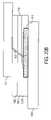
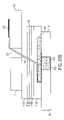
- FIG. 11Ashows a side view of an electrochemical device according to an exemplary embodiment of the present invention.
- a first contact 1101is coupled with bonding layer 1110 with a portion of the first contact 1101 extending past the bonding layer 1110 .
- the bonding layer 1110may also be bonded with the cell structure 1115 .
- a second contact 1105is placed under the cell structure 1115 .
- a barrier layerfor example, may also be placed between the second contact 1105 and the cell structure 1115 .
- Shown embedded within the bonding layer 1110is conductor 1120 . This conductor 1120 , for example, creates a selectively conductive bonding layer.
- a selectively conductive bonding layer 1110permits conduction from the cell structure 1115 through the bonding layer 1110 to the first contact 1101 at specific points, and yet provides insulation between the first contact 1101 and the second contact 1105 .
- the conductor 1120may be placed within the bonding layer 1110 in many different ways. For example, a metal tab, a metal wire, multiple metal wires, a metal wire mesh, perforated metal foil, perforated metal, a metal coating applied to the adhesive layer, a metallic disk, a metallically coated fiberglass or combinations thereof may be used. In each of these examples, the conductor 1120 can provide electrical conduction between the cell structure 1115 and the first contact 1101 and yet provide insulation between the two contacts 1101 , 1105 . In some embodiments the conductor 1120 may be woven within the bonding layer 1110 . The conductor 1115 may be, for example, disks embedded within the bonding layer 1110 .
- slits within the bonding layer 1110may be made in order to weave or place the conductor 1120 through the bonding layer 1110 . Also, for example, holes or other means may be used to place the conductor 1120 through the bonding layer 1110 .
- a reinforcement layermay be placed within the insulating layer.
- a fiberglass materialmay cover half of one surface of the insulating layer, woven through the layer and then cover the other half of the bonding layer.
- Such a layer of fiberglass without a conductive coatingwould insulate the materials placed between.
- the fiberglassmay be coated in a localized area with a conductive material.
- Such conductive coatingscan coat the fiberglass area at the top and bottom surface of the bonding layer.
- the fiberglasswould conduct between the upper contact and the cell.
- Conductive materialmay be disposed on the fiberglass using ink jet, silk screen, plasma deposition, e-beam deposition, spray and/or brush methods. Other materials may be used rather than fiberglass, such as, for example, KEVLAR®, plastic, glass or other insulating materials.
- An exemplary embodiment of the present inventionprovides for selective contact between the first contact and the cell structure through holes in the bonding layer.
- holes in the bonding layermay allow the first contact and cell structure to remain in contact.
- the layersmay be, for example, pressed together to create a contact.
- conductive glues or inksmay be applied in or near the hole area in the bonding layer to make the contact between the layers.
- Lithiummay also be used as a conductive material.
- the conductor 1120may be made of gold, platinum, stainless steel, titanium, zirconium, cobalt, aluminum, indium, nickel, copper, silver, carbon, bronze, brass, beryllium, or oxides, nitrides, and alloys thereof.
- FIG. 11Bshows a top view of the exemplary embodiment shown in FIG. 11A .
- the first contact 1101extends past the bonding layer 1110 and the second contact 1105 .
- the second contact 1105also extends past the boding layer 1115 and the first contact 1101 in the opposite direction.
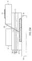
- FIGS. 11C and 11Dshow an exemplary embodiment in which leads are formed from the first and second contacts 1101 , 1105 .
- a first partial cut 1140 ais made in the first contact 1101 and a partial cut 1140 b is made in the second contact 1105 .
- These partial cutsform strips that may be folded over to extend from the electrochemical device.
- FIG. 11Dshows an example in which strips 1142 a and 1142 b resulting from the partial cuts in the contacts 1101 , 1105 are folded in a downward direction of the drawing. It should be appreciated that only one or both of the extending parts of the contacts 1101 , 1105 can be partially cut to form leads in a variety of ways for a desired application or orientation of the electrochemical device.
- FIGS. 12A-19Bshow individual layers and parts of this embodiment and how they can be coupled or bonded together. These figures are not meant to show a step-by-step process for manufacturing any embodiments of the invention. Rather, these figures are presented to help understand how the layers interact.
- FIGS. 12A , 13 A, 14 A, 15 A, 16 A, 17 A, 18 A and 19 Ashow side views of various parts of an exemplary battery
- FIGS. 12B , 13 B, 14 B, 15 B, 16 B, 17 B, 18 B and 19 Bshow top views.
- FIG. 12Ashows a side view of a conductor 1120 according to one embodiment of the present invention.
- the top view of three exemplary types of conductors, a wire 1121 , a tab 1122 , and a wire mesh 1123are shown in FIG. 12B .
- FIG. 13Ashows a side view and FIG. 13B shows a top view of a slit 1130 cut within a bonding layer 1110 .
- FIG. 14Ashows a side view of a conductor 1120 , for example, woven through the bonding layer.
- FIG. 14Bshows a top view of a mesh wire conductor 1123 woven through the bonding layer 1110 .
- FIG. 15Ashows the conductor 1120 embedded within the bonding layer.
- the conductor 1120may be embedded within the bonding layer 1110 , for example, by heating the bonding layer 1110 to the point where the conductor 1120 may be pressed within the bonding layer 1110 .
- the surfaces of the conductor 1120 and bonding layer 1110may preferably be flush after this process.
- FIG. 15Bshows a top view of a wire mesh conductor 1123 embedded within the bonding layer.
- the resultant bonding layer 1110 from FIGS. 12A-15Bshow a bonding layer with insulating properties yet provides selective conductivity between the portions of the top surface and the lower surface of the bonding layer 1120 .
- Other combinationmay also produce selective conductivity.
- FIG. 16A and FIG. 16Bshow a first contact 1101 .
- FIG. 17Ashows the first contact 1101 bonded with the bonding layer 1110 .
- the conductor 1120preferably makes electrical contact with the first electrical contact 1101 .
- FIG. 17Bshows the top view of FIG. 17A .
- the first contactmay also encapsulate the battery thereby protecting it from environmental degradation and damage.
- many electrochemical devicescomprise environmentally sensitive materials such as Lithium. These materials can be extremely reactive with air and moisture, and may degrade when exposed to such environments. Accordingly, the first contact 1101 may encapsulate the battery to protect it from environmentally sensitive materials in the electrochemical device from air and/or moisture.
- FIG. 18Ashows an exemplary embodiment of a single battery cell 1115 coupled with a second contact 1105 .
- the second contact 1105may also be the substrate upon which the cell is deposited.
- the cell structure in this embodimentcomprises a cathode, and anode and an electrolyte.
- the electrolytemay include LIPON.
- FIG. 19Ashows a completed cell structure.
- the second contact 1105 and the cell structure 1115 from FIG. 18Aare coupled with the first contact 1101 and the bonding layer 1110 as shown in 17 A.
- the conductor 1120is preferably in electrical contact with the electrochemical device 1115 in a selective area.
- the cellis bounded by external contacts 1101 and 1105 with minimal layers there between. In this embodiment the first and second contacts 1101 and 1105 extend beyond the area of the electrochemical device 1115 .
- the first and second contacts 1101 , 1105 of this embodimentcan be made of a conductive metal.
- the contact or contactsmay be made of gold, platinum, stainless steel, titanium, zirconium, cobalt, aluminum, indium, nickel, copper, silver, carbon, bronze, brass, beryllium, or oxides, nitrides, and alloys thereof. Other conductive materials may also be used.
- electrical contact between the cell structure 1115 and first electrical contact 1101may be provided by a number of other ways.
- electrical conduction between the cell structure 1115 and the first contact 1101may be provided by embedding a conductive powder within an adhesive forming the bonding layer 1110 .
- a conductive powdersuch as a metallic powder (e.g., nickel powder) can be embedded in an adhesive bonding layer 1110 at one or more selected areas within an adhesive bonding layer 1110 and between the contact 1101 and the cell structure 1115 .
- FIG. 20Ashows a side view of a bonding layer according to an exemplary embodiment of the present invention.
- the bonding layer 1110can be a composite of two layers: the upper layer 1110 A being in contact with the first contact 1101 and the lower layer 1110 B being in contact with the cell structure 1115 .
- the lower layer 1110 Bmay have chemical compatibility, chemical stability, chemical resistance, chemical non-reactivity, and chemical robustness with the cell structure 1115 .
- the top layer 1110 Amay have a melting point preferably higher than 100° C. and pressure resilience against at least 10 psi so that the composite bonding layer has an enhanced heat and pressure resiliency compared to the bonding layer 1110 .
- the conductor 1120may be embedded through both the layers of 1110 A aid 1110 B.
- the lower layer 1110 Bcan be, for example, a copolymer, which may be a thermoplastic or thermally set.
- the lower layer 1110 Bcan be an ethylene methacrylic acid (E/MAA) copolymer.
- the lower layer 1110 Bcan be an ethylene methacrylic acid (E/MAA) copolymer, in which part of the methacrylic acid is neutralized with metal ions such as zinc (Zn) or sodium (Na).
- the lower layer 1110 Bmay comprise at least one polymer type selected from the group of cyano-acrylates, epoxies, fluoro-acrylates, polyimides containing ether linkages, urea-formaldehyde resins, vinyl chlorides, and low-density polyethylene (LDPE).
- LCPElow-density polyethylene
- the upper layer 1110 Acan comprise at least one polymer type selected from the group of polyamides (e.g., Nylon), polyimides (e.g., Kapton), polyethylene terephthalates (e.g., Mylar), para-aramids (e.g., Kevlar), polyethylenes, high-density polyethylenes (e.g., Valeron), Ultra High Molecular Weight (UHMW) polyethylenes, polypropylenes, acrylics, polycarbonates, polyvinyl chlorides (PVC and CPVC), Acetal Delrin, phenolics, fluoroplastics (e.g., Teflon), polyurethanes, polystyrenes (e.g., acrylonitrile-butadiene-styrenes [ABS]), Keton PEEK, Tenite resins (e.g., Butyrate), silicate or non-silicate based glass, fiberglass, oxide ceramic (e.g., Z
- FIG. 20Bshows a side view of a bonding layer according to another exemplary embodiment of the present invention.
- the bonding layer 1110may have three layers: the topmost layer 1110 D being in contact with the first contact 1101 and the lowest layer 1110 F being in contact with the cell structure 1115 .
- the middle layer 1110 Emay be in contact with the layers 1110 D and 1110 F, but 1110 E may not contact with 1101 and 1115 .
- the topmost layer 1110 Dmay have chemical compatibility, chemical stability, chemical resistance, chemical non-reactivity, and chemical robustness with the first contact 1101 .
- the lowest layer 1110 Fmay have chemical compatibility, chemical stability, chemical resistance, chemical non-reactivity, and chemical robustness with the cell structure 1115 .
- the middle layer 1110 Ethe so-termed heat and pressure resilient layer (HAPR layer) may have a melting point preferably higher than 100° C. and a pressure resilience against at least 10 psi, so that the composite bonding layer may possess an enhanced heat and pressure resiliency.
- FIG. 20Cshows a side view of a bonding layer according to another exemplary embodiment of the present invention.
- an adhesion layer 1110 Gcan be added in between layers 1110 D and 1110 E.
- FIG. 20Dshow a side view of another exemplary embodiment in which bonding layer 1110 may comprise an adhesion layer 1110 H in between 1110 F and 1110 E.
- FIG. 20Eshows yet another exemplary embodiment in which both layers 1110 G and 1110 H can be added in between 1110 F and 1110 E.
- the adhesion layers 1110 G and 1110 Hcan be the same or different.
- the layers 1110 D and 1110 Fcan be same or different also.
- the conductor 1120may be embedded through all the layers of 1110 D, 1110 E and 1110 F, including 1110 G and 1110 H layers, when they are present.
- the topmost layer 1110 Dcan be, for example, a copolymer, an ethylene methacrylic acid (E/MAA) copolymer, or an ethylene methacrylic acid (E/MAA) copolymer, in which part of the methacrylic acid is neutralized with metal ions such as zinc (Zn) or sodium (Na).
- the topmost layer 1110 Dmay comprise at least one polymer type selected from the group of cyano-acrylates, epoxies, fluoro-acrylates, polyimides containing ether linkages, urea-formaldehyde resins, vinyl chlorides, and low-density polyethylene (LDPE).
- the HAPR layer 1110 Emay comprise at least one polymer type selected from the group of polyamides (e.g., Nylon), polyimides (e.g., Kapton), polyethylene terephthalates (e.g., Mylar), para-aramids (e.g., Kevlar), polyethylenes, high-density polyethylenes (e.g., Valeron), Ultra High Molecular Weight (UHMW) polyethylenes, polypropylenes, acrylics, polycarbonates, polyvinyl chlorides (PVC and CPVC), Acetal Delrin, phenolics, fluoroplastics (e.g., Teflon), polyurethanes, polystyrenes (e.g., acrylonitrile-butadiene-styrenes [ABS]), Keton PEEK, Tenite resins (e.g., Butyrate), oxide ceramic (e.g., ZrO 2 ), nitride, polyamides (e.
- the lowest layer 1110 Fmay be, for example, a copolymer, an ethylene methacrylic acid (E/MAA) copolymer, or an ethylene methacrylic acid (E/MAA) copolymer, in which part of the methacrylic acid may be neutralized with metal ions such as zinc (Zn) or sodium (Na).
- the lowest layer 1110 Fmay comprise at least one polymer type selected from the group of cyano-acrylates, epoxies, fluoro-acrylates, polyimides containing ether linkages, urea-formaldehyde resins, vinyl chlorides, and low-density polyethylene (LDPE).
- the conductor 1120may, for example, comprise at least one element selected from the group of Li, B, graphitic carbon, Al, Si, Sc, Ti, V, Cr, Mn, Fe, Co, Ni, Cu, Y, Zr, Nb, Mo, Ru, Rh, Pd, Ag, In, Sn, Hf, Ta, W, Re, Os, Ir, Pt, Au, Pb, and any alloy thereof, including stainless steel, and is made by rolling, electroforming, drawing or any other materials processing technique or any vacuum deposition technique, such as sputtering, evaporation or CVD, or an electrochemical process (e.g., electroplating or electroless plating).
- the conductor 1120may, for example, comprise at least one element selected from the group of Li, B, graphitic carbon, Al, Si, Sc, Ti, V, Cr, Mn, Fe, Co, Ni, Cu, Y, Zr, Nb, Mo, Ru, Rh, Pd, Ag, In, Sn, Hf, Ta, W,
- FIG. 21shows a side view of a bonding layer according to an exemplary embodiment of the present invention.
- the bonding layer 1110may be, partly or completely, an isotropic or anisotropic adhesive layer 1110 I comprising at least one adhesive selected from the group of ethylene methacrylic acid (E/MAA) copolymer, ethylene methacrylic acid metallate (E/MAA) copolymer, cyano-acrylates, epoxies, fluoro-acrylates, polyimides containing ether linkages, urea-formaldehyde resins, vinyl chlorides, and low-density polyethylene (LDPE) that may contain gold-coated polymer spheres, solder-type alloys, or solid metal powders such as carbon, Ni, Au, Cu, or Ag.
- E/MAAethylene methacrylic acid
- E/MAAethylene methacrylic acid metallate copolymer
- cyano-acrylatesepoxies
- the adhesive materialcould be thermally set (for strong and reliable bonding) or thermoplastic (to facilitate the rework process).
- the isotropic or anisotropic adhesivemay replace the conductor 1120 , at least one of the layers from the group of 1110 A, 1110 B, 1110 D, 1110 E, 1110 F, 1110 G, and 1110 H, or both.
- FIG. 22shows a view of a conductor according to an exemplary embodiment of the present invention.
- the conductor 1120may have (one, two, three or many) conducting strips ( 1120 A and 1120 B, for example) attached.
- the strips ( 1120 A, and 1120 B)may be made by rolling, electroforming, drawing or any other materials processing technique, or any vacuum deposition technique, such as sputtering, evaporation or CVD, or an electrochemical process (e.g., electroplating or electroless plating).
- the strip-forming processmay involve a deposition mask.
- the strip materialcan be chosen such that it could form a good metallurgical bond with the anode material (e.g., Li).
- the metallurgical bondmay either be created via a solid solution or through an alloy compound.
- the stripmay be made of metal, such as Li, B, graphitic carbon, Al, Si, Sc, Ti, V, Cr, Mn, Fe, Co, Ni, Cu, Y, Zr, Nb, Mo, Ru, Rh, Pd, Ag, In, Sn, Hf, Ta, W, Re, Os, Ir, Pt, Au, Pb, and any alloy thereof, including stainless steel, wherein Li, Ni or Cu are, for example, the most preferred material selections.
- the strips ( 1120 A and 1120 B)may be bent at an angle of a few degrees (for example, 5 degrees) to, for example, 90 degrees with respect to the longest dimension of the conductor 1120 .
- the strip 1120 Afor example, is bent to form a 90 degree angle 2202 A with respect to the longest dimension of the conductor 1120 .
- the strip 1120 Bfor example, is bent to form a 5 degree angle 2202 B with respect to the longest dimension of the conductor 1120 .
- the length and width of the stripsmay range from several micrometers to tens of millimeters.
- the thicknessmay range from 1/100 th of a micrometer up to tens of micrometers.
- the stripsare 3 mm long, 0.3 mm wide and 0.01 mm thick.
- FIG. 25shows a side view of an exemplary embodiment of the present invention including an anode.
- a protection layer 600 Acan be deposited on the anode 600 .
- the protection layer 600 Amay provide electrical contact from the anode 600 to the outside terminal 800 and at the same time provides environmental protection from exposure to moisture, oxygen and environmental species.
- the protection layer 600 Acan be made of an oxide, nitride, carbide or carbonate.
- the protection layer 600 Amay be made of a metal that is vapor-deposited (CVD or PVD) with the help of a shadow mask.
- the protection layer 600 Amay be made of Ni or Cu.
- FIG. 23Ashows a side view of a bonding layer according to an exemplary embodiment of the present invention.
- the first contact 1101can be, for example, a non-conducting, insulating, or semiconducting layer.
- An opening 2301may be created (either by mechanical means or masking during formation of the layer) in the non-conducting, insulating, or semiconducting layer 1101 so that the conductor 1120 could be used to contact the cell structure 1115 for termination purposes.
- a conducting inserte.g., a metal or an isotropic/anisotropic conducting adhesive
- the non-conducting, insulating, or semiconducting layer 1101may be a ceramic selected from the group comprising BeO, B 2 O 3 , BN, borate glass, Al 2 O 3 , AlN, SiO 2 , Si 3 N 4 , silicate glass, ScO x , TiO x , VO x , CrO x , FeO x , YO x , ZrO x , NbO x , MoO x , HfO x , TaO x , WO x , a nitride ceramic, a carbide ceramic, or a combination thereof.
- the non-conducting layer 1101may also comprise at least one polymer type selected from the group of polyamides (e.g., Nylon), polyimides (e.g., Kapton), polyethylene terephthalates (e.g., Mylar), para-aramids (e.g., Kevlar), polyethylenes, high-density polyethylenes (e.g., Valeron), Ultra High Molecular Weight (UHMW) polyethylenes, polypropylenes, acrylics, polycarbonates, polyvinyl chlorides (PVC and CPVC), Acetal Delrin, phenolics, fluoroplastics (e.g., Teflon), polyurethanes, polystyrenes (e.g., acrylonitrile-butadiene-styrenes [ABS]), Keton PEEK, Tenite resins (e.g., Butyrate) or a combination/modification thereof.
- the semiconducting layer 1101may be Si, Ge
- the non-conducting layer 1101may also have printed circuitry 2305 and the cell structure 1115 may be connected into the circuitry 2305 through an opening 2301 through the non-conducting layer 1101 either through the conductor 1120 or by the use of an isotropic or anisotropic conducting adhesive.
- the openingmay be created either by mechanical means or masking/etching.
- the non-conducting layer 1101may be equipped with at least one electrical connection layer that goes over at least one edge of the non-conducting layer 1101 and makes electrical contact with both the cell structure 1115 and the printed circuitry 2305 which are sandwiching the non-conducting layer 1101 .
- the electrical connection layermay comprise a conducting medium comprising Li, B, graphitic carbon, Al, Si, Sc, Ti, V, Cr, Mn, Fe, Co, Ni, Cu, Y, Zr, Nb, Mo, Ru, Rh, Pd, Ag, In, Sn, Hf, Ta, W, Re, Os, Ir, Pt, Au, Pb, and any alloy thereof, including stainless steel, wherein Ni or Cu are the most preferred material selections.
- the non-conducting layer 1101may provide another protective metallic layer, with or without a bonding layer in between the non-conducting and protective layers.
- the bonding layermay comprise at least one polymer type selected from the group of ethylene methacrylic acid (E/MAA) copolymer, ethylene methacrylic acid metal late (E/MAA) copolymer, cyano-acrylates, epoxies, fluoro-acrylates, polyimides containing ether linkages, urea-formaldehyde resins, vinyl chlorides, and low-density polyethylene (LDPE).
- E/MAAethylene methacrylic acid
- E/MAAethylene methacrylic acid metal late copolymer
- cyano-acrylatesepoxies
- fluoro-acrylatespolyimides containing ether linkages
- urea-formaldehyde resinsvinyl chlorides
- low-density polyethylene (LDPE)low-density polyethylene
- the bonding layer 1110 in this exemplary embodimentmay be used as a heat and pressure resilient layer, without any further reinforcements, because the non-conducting layer does not cause any electrical shorting to the second contact 1105 when the bonding layer is damaged.
- a reinforcement structure(a two-layer, three-layer, four-layer, or five layer structure, as illustrated above) may be used in place of the bonding layer.
- FIG. 23Bshows a side view of a bonding layer according to an exemplary embodiment of the present invention.
- the second contact 1105is a non-conducting layer.
- An opening 2302may be created, either by mechanical means or masking during formation of the layer, in the non-conducting layer 1105 so that a conductor 1190 (hole-filling metallic column of Au, for instance) could be used to contact the cell structure 1115 for termination purposes.
- a conducting inserte.g., a metal or an isotropic/anisotropic conducting adhesive
- the non-conducting layer 1105may be a ceramic selected from the group comprising BeO, B 2 O 3 , BN, borate glass, Al 2 O 3 , AlN, SiO 2 , Si 3 N 4 , silicate glass, ScO x , TiO x , VO x , CrO x , FeO x , YO x , ZrO x , NbO x , MoO x , HfO x , TaO x , WO x , or a combination thereof.
- the bonding layer 1110may be used as a heat and pressure resilient layer, without any further reinforcements, because the non-conducting layer 1105 does not cause any electrical shorting to the first contact 1101 when the bonding layer is damaged.
- the first contact 1101may be eliminated for this invention.
- the conductor 1120could be used for electrically contacting the cell structure 1115 for termination purposes.
- FIG. 24shows a side view of an exemplary embodiment according to the current invention, in which the first contact 1101 of a first thin-film battery may be replaced by a second thin-film battery, which has all of the layers in FIG. 11A ( 1101 ′, 1110 D′, 1110 G′, 1110 E′, 1110 F′, 1110 H′, 1115 ′, and 1105 ′), that is head-on attached to the bonding layer 1110 of the first thin-film battery.
- the said head-on attached second thin-film batterymay not necessarily possess all of the layers shown in FIG. 11A and may have any of the layers 1101 , 1110 , and 1120 missing.
- two thin-film batteriesmay be attached to each other via one or multiple bonding layer(s) as detailed above. It is this head-on second thin-film battery that may serve as the heat-and-pressure resilient encapsulation to the first thin-film battery.
- the first contact 1101may be covered by an electrically insulating and mechanically robust film comprising Lipon, borides, carbides, nitrides, oxides, polyamides, polyimides, polyethylene terephthalates, para-aramids, polyethylenes, high-density polytheylenes, Ultra High Molecular Weight (UHMW) polyethylenes, polypropylenes, acrylics, polycarbonates, polyvinyl chlorides, acetal delrin, phenolics, fluoroplastics, polyurethanes, polystyrenes, acrylonitrile-butadiene-styrenes (ABS), Keton PEEK, and/or Tenite resins.
- an electrically insulating and mechanically robust filmcomprising Lipon, borides, carbides, nitrides, oxides, polyamides, polyimides, polyethylene terephthalates, para-aramids, polyethylenes, high-density polytheylenes, Ultra High Molecular Weight (
- the borides, carbides, nitrides, and/or oxidesmay be configured with boron, aluminum, silicon, Ti, Ta, Zr, Hf or a similar element, or a modification/combination thereof.
- the insulating filmmay mechanically and electrically protect the first contact 1101 from damages.
- a recessmay be created, by a shadow mask during or after the formation of the insulation film, in the first contact 1101 in order for it to make contact with the conductor 1120 .
- another conductormay also be used in the central portion for contacting the conductor 1120 .
- an isotropic or anisotropic conducting adhesivemay be used in the central portion for contacting the conductor 1120 for termination purposes.
- the isotropic or anisotropic adhesivemay comprise at least one adhesive selected from the group of ethylene methacrylic acid (E/MAA) copolymer, ethylene methacrylic acid metallate (E/MAA) copolymer, cyano-acrylates, epoxies, fluoro-acrylates, polyimides containing ether linkages, urea-formaldehyde resins, vinyl chlorides, and low-density polyethylene (LDPE) that contains gold-coated polymer spheres, solder-type alloys, or solid metal powders such as carbon, Ni, Au, Cu, or Ag.
- E/MAAethylene methacrylic acid
- E/MAAethylene methacrylic acid metallate copolymer
- cyano-acrylatesepoxies
- fluoro-acrylatesfluoro-acrylates
- polyimides containing ether linkagesurea-formaldehyde resins
- vinyl chloridesvinyl chlorides
- LDPElow-
- the conductor 1120may not be a necessary component of the current invention.
- the contact between the first contact 1101 and the cell structure 1115can be made by applying pressure by a mandrel in the central portion of the first contact 1101 so that a depression is created in the first contact 1101 thereby creating an electrical contact.
- the bonding layer 1110can be removed before creating the depression of 1101 by the mandrel so as to create a more robust electrical contact between the first contact and the cell structure.
Landscapes
- Chemical & Material Sciences (AREA)
- Chemical Kinetics & Catalysis (AREA)
- Electrochemistry (AREA)
- General Chemical & Material Sciences (AREA)
- Engineering & Computer Science (AREA)
- Manufacturing & Machinery (AREA)
- Connection Of Batteries Or Terminals (AREA)
- Sealing Battery Cases Or Jackets (AREA)
- Battery Mounting, Suspending (AREA)
- Secondary Cells (AREA)
- Primary Cells (AREA)
Abstract
Description
Claims (24)
Priority Applications (8)
| Application Number | Priority Date | Filing Date | Title |
|---|---|---|---|
| US12/111,388US8394522B2 (en) | 2002-08-09 | 2008-04-29 | Robust metal film encapsulation |
| KR1020107026825AKR101522064B1 (en) | 2008-04-29 | 2009-04-24 | Robust metal film encapsulation |
| JP2011507550AJP6063625B2 (en) | 2008-04-29 | 2009-04-24 | Robust metal membrane encapsulation |
| PCT/US2009/041664WO2009134689A2 (en) | 2008-04-29 | 2009-04-24 | Robust metal film encapsulation |
| EP09739491.0AEP2272120B1 (en) | 2008-04-29 | 2009-04-24 | Robust metal film encapsulation |
| CN200980124956.XACN102067356B (en) | 2008-04-29 | 2009-04-24 | Rugged metal film coating |
| TW98114234ATWI469421B (en) | 2008-04-29 | 2009-04-29 | Robust metal film encapsulation |
| JP2015172215AJP6155425B2 (en) | 2008-04-29 | 2015-09-01 | Battery |
Applications Claiming Priority (9)
| Application Number | Priority Date | Filing Date | Title |
|---|---|---|---|
| US10/215,190US6916679B2 (en) | 2002-08-09 | 2002-08-09 | Methods of and device for encapsulation and termination of electronic devices |
| US11/374,282US20080003496A1 (en) | 2002-08-09 | 2005-06-15 | Electrochemical apparatus with barrier layer protected substrate |
| US11/209,536US8021778B2 (en) | 2002-08-09 | 2005-08-23 | Electrochemical apparatus with barrier layer protected substrate |
| US73761305P | 2005-11-17 | 2005-11-17 | |
| US75947906P | 2006-01-17 | 2006-01-17 | |
| US78279206P | 2006-03-16 | 2006-03-16 | |
| US11/561,277US8445130B2 (en) | 2002-08-09 | 2006-11-17 | Hybrid thin-film battery |
| US11/687,032US8236443B2 (en) | 2002-08-09 | 2007-03-16 | Metal film encapsulation |
| US12/111,388US8394522B2 (en) | 2002-08-09 | 2008-04-29 | Robust metal film encapsulation |
Related Parent Applications (1)
| Application Number | Title | Priority Date | Filing Date |
|---|---|---|---|
| US11/687,032Continuation-In-PartUS8236443B2 (en) | 2002-08-09 | 2007-03-16 | Metal film encapsulation |
Publications (2)
| Publication Number | Publication Date |
|---|---|
| US20080261107A1 US20080261107A1 (en) | 2008-10-23 |
| US8394522B2true US8394522B2 (en) | 2013-03-12 |
Family
ID=41255703
Family Applications (1)
| Application Number | Title | Priority Date | Filing Date |
|---|---|---|---|
| US12/111,388Active2030-11-04US8394522B2 (en) | 2002-08-09 | 2008-04-29 | Robust metal film encapsulation |
Country Status (7)
| Country | Link |
|---|---|
| US (1) | US8394522B2 (en) |
| EP (1) | EP2272120B1 (en) |
| JP (2) | JP6063625B2 (en) |
| KR (1) | KR101522064B1 (en) |
| CN (1) | CN102067356B (en) |
| TW (1) | TWI469421B (en) |
| WO (1) | WO2009134689A2 (en) |
Cited By (3)
| Publication number | Priority date | Publication date | Assignee | Title |
|---|---|---|---|---|
| US20180069261A1 (en)* | 2016-07-26 | 2018-03-08 | Varta Microbattery Gmbh | Electrochemical cell |
| US10660208B2 (en) | 2016-07-13 | 2020-05-19 | General Electric Company | Embedded dry film battery module and method of manufacturing thereof |
| US11101513B2 (en) | 2018-09-04 | 2021-08-24 | International Business Machines Corporation | Thin film battery packaging |
Families Citing this family (28)
| Publication number | Priority date | Publication date | Assignee | Title |
|---|---|---|---|---|
| US20070264564A1 (en) | 2006-03-16 | 2007-11-15 | Infinite Power Solutions, Inc. | Thin film battery on an integrated circuit or circuit board and method thereof |
| US7993773B2 (en)* | 2002-08-09 | 2011-08-09 | Infinite Power Solutions, Inc. | Electrochemical apparatus with barrier layer protected substrate |
| US8236443B2 (en) | 2002-08-09 | 2012-08-07 | Infinite Power Solutions, Inc. | Metal film encapsulation |
| US8431264B2 (en) | 2002-08-09 | 2013-04-30 | Infinite Power Solutions, Inc. | Hybrid thin-film battery |
| US8394522B2 (en)* | 2002-08-09 | 2013-03-12 | Infinite Power Solutions, Inc. | Robust metal film encapsulation |
| US8404376B2 (en) | 2002-08-09 | 2013-03-26 | Infinite Power Solutions, Inc. | Metal film encapsulation |
| US8445130B2 (en) | 2002-08-09 | 2013-05-21 | Infinite Power Solutions, Inc. | Hybrid thin-film battery |
| US8021778B2 (en) | 2002-08-09 | 2011-09-20 | Infinite Power Solutions, Inc. | Electrochemical apparatus with barrier layer protected substrate |
| US8728285B2 (en) | 2003-05-23 | 2014-05-20 | Demaray, Llc | Transparent conductive oxides |
| KR101127370B1 (en) | 2004-12-08 | 2012-03-29 | 인피니트 파워 솔루션스, 인크. | Deposition of licoo2 |
| US7959769B2 (en) | 2004-12-08 | 2011-06-14 | Infinite Power Solutions, Inc. | Deposition of LiCoO2 |
| JP2010505044A (en) | 2006-09-29 | 2010-02-18 | インフィニット パワー ソリューションズ, インコーポレイテッド | Material constraints for masking flexible substrates and depositing battery layers on flexible substrates |
| US8197781B2 (en) | 2006-11-07 | 2012-06-12 | Infinite Power Solutions, Inc. | Sputtering target of Li3PO4 and method for producing same |
| US8268488B2 (en)* | 2007-12-21 | 2012-09-18 | Infinite Power Solutions, Inc. | Thin film electrolyte for thin film batteries |
| US9334557B2 (en) | 2007-12-21 | 2016-05-10 | Sapurast Research Llc | Method for sputter targets for electrolyte films |
| JP5705549B2 (en)* | 2008-01-11 | 2015-04-22 | インフィニット パワー ソリューションズ, インコーポレイテッド | Thin film encapsulation for thin film batteries and other devices |
| US8350519B2 (en) | 2008-04-02 | 2013-01-08 | Infinite Power Solutions, Inc | Passive over/under voltage control and protection for energy storage devices associated with energy harvesting |
| WO2010019577A1 (en) | 2008-08-11 | 2010-02-18 | Infinite Power Solutions, Inc. | Energy device with integral collector surface for electromagnetic energy harvesting and method thereof |
| JP5650646B2 (en) | 2008-09-12 | 2015-01-07 | インフィニット パワー ソリューションズ, インコーポレイテッド | Energy device with integral conductive surface for data communication via electromagnetic energy and method for data communication via electromagnetic energy |
| WO2010042601A1 (en)* | 2008-10-08 | 2010-04-15 | Infinite Power Solutions, Inc. | Foot-powered footwear-embedded sensor-transceiver |
| WO2010042594A1 (en) | 2008-10-08 | 2010-04-15 | Infinite Power Solutions, Inc. | Environmentally-powered wireless sensor module |
| WO2011028825A1 (en)* | 2009-09-01 | 2011-03-10 | Infinite Power Solutions, Inc. | Printed circuit board with integrated thin film battery |
| EP2522043B1 (en)* | 2009-10-14 | 2019-05-15 | Greatbatch Ltd. | Temporary insulator for battery packs and associated systems and methods |
| KR101930561B1 (en) | 2010-06-07 | 2018-12-18 | 사푸라스트 리써치 엘엘씨 | Rechargeable high-density electrochemical device |
| FR2975229B1 (en) | 2011-05-13 | 2013-07-05 | Commissariat Energie Atomique | STACKING ARCHITECTURE AND / OR ELECTRIC POWER GENERATING ELEMENT WITH CONFIGURABLE ELECTRICAL OUTPUT, METHOD OF MAKING SUCH A ARCHITECTURE |
| FR2980305A1 (en)* | 2011-09-19 | 2013-03-22 | St Microelectronics Tours Sas | METHOD FOR ENCAPSULATING AN ELECTRIC ENERGY ACCUMULATION MEMBER AND BATTERY |
| DE102014117640A1 (en)* | 2014-12-01 | 2016-06-02 | Schott Ag | Electrical storage system with disc discrete element, discrete element, process for its manufacture and its use |
| CN112510295A (en)* | 2020-11-30 | 2021-03-16 | 南通路远科技信息有限公司 | Battery with polymer shell |
Citations (715)
| Publication number | Priority date | Publication date | Assignee | Title |
|---|---|---|---|---|
| US712316A (en) | 1899-10-26 | 1902-10-28 | Francois Loppe | Electric accumulator. |
| US1712316A (en) | 1925-12-16 | 1929-05-07 | Henry L F Trebert | Hydraulic brake |
| US2970180A (en)* | 1959-06-17 | 1961-01-31 | Union Carbide Corp | Alkaline deferred action cell |
| US3309302A (en) | 1963-10-07 | 1967-03-14 | Varian Associates | Method of preparing an electron tube including sputtering a suboxide of titanium on dielectric components thereof |
| US3616403A (en) | 1968-10-25 | 1971-10-26 | Ibm | Prevention of inversion of p-type semiconductor material during rf sputtering of quartz |
| US3790432A (en) | 1971-12-30 | 1974-02-05 | Nasa | Reinforced polyquinoxaline gasket and method of preparing the same |
| US3797091A (en) | 1972-05-15 | 1974-03-19 | Du Pont | Terminal applicator |
| US3850604A (en) | 1972-12-11 | 1974-11-26 | Gte Laboratories Inc | Preparation of chalcogenide glass sputtering targets |
| US3939008A (en) | 1975-02-10 | 1976-02-17 | Exxon Research And Engineering Company | Use of perovskites and perovskite-related compounds as battery cathodes |
| US4082569A (en) | 1977-02-22 | 1978-04-04 | The United States Of America As Represented By The Administrator Of The National Aeronautics And Space Administration | Solar cell collector |
| US4111523A (en) | 1973-07-23 | 1978-09-05 | Bell Telephone Laboratories, Incorporated | Thin film optical waveguide |
| US4127424A (en) | 1976-12-06 | 1978-11-28 | Ses, Incorporated | Photovoltaic cell array |
| US4226924A (en) | 1977-11-22 | 1980-10-07 | Asahi Kasei Kogyo Kabushiki Kaisha | Thin metal-halogen cells |
| US4283216A (en) | 1978-12-11 | 1981-08-11 | Triplex Safety Glass Company Limited | Producing glass sheets of required curved shape |
| US4318938A (en) | 1979-05-29 | 1982-03-09 | The University Of Delaware | Method for the continuous manufacture of thin film solar cells |
| US4328297A (en) | 1981-03-27 | 1982-05-04 | Yardngy Electric Corporation | Electrode |
| US4395713A (en) | 1980-05-06 | 1983-07-26 | Antenna, Incorporated | Transit antenna |
| US4437966A (en) | 1982-09-30 | 1984-03-20 | Gte Products Corporation | Sputtering cathode apparatus |
| US4442144A (en) | 1980-11-17 | 1984-04-10 | International Business Machines Corporation | Method for forming a coating on a substrate |
| US4467236A (en) | 1981-01-05 | 1984-08-21 | Piezo Electric Products, Inc. | Piezoelectric acousto-electric generator |
| US4481265A (en) | 1982-06-11 | 1984-11-06 | Hitachi, Ltd. | Photovoltaic-storage battery device |
| US4518661A (en) | 1982-09-28 | 1985-05-21 | Rippere Ralph E | Consolidation of wires by chemical deposition and products resulting therefrom |
| US4555456A (en) | 1983-05-26 | 1985-11-26 | Hitachi, Ltd. | Cathode structure for thin film battery |
| US4572873A (en) | 1982-09-13 | 1986-02-25 | Hitachi, Ltd. | Titanium disulfide thin film and process for fabricating the same |
| US4587225A (en) | 1983-10-17 | 1986-05-06 | Toyo Soda Manufacturing Co., Ltd. | High-strength zirconia type sintered body |
| US4619680A (en) | 1984-06-11 | 1986-10-28 | The General Electric Co. P.L.C. | Manufacture of integrated optical waveguides |
| US4645726A (en) | 1984-11-26 | 1987-02-24 | Hitachi, Ltd. | Solid state lithium battery |
| US4664993A (en) | 1981-08-24 | 1987-05-12 | Polaroid Corporation | Laminar batteries and methods of making the same |
| US4668593A (en) | 1986-08-29 | 1987-05-26 | Eltron Research, Inc. | Solvated electron lithium electrode for high energy density battery |
| US4672586A (en) | 1983-06-06 | 1987-06-09 | Hitachi, Ltd. | Semiconductor memory having circuit effecting refresh on variable cycles |
| USRE32449E (en) | 1983-06-16 | 1987-06-30 | Max-Planck-Gesellschaft Zur Forderung Der Wissenschaften E.V | Ceramic body of zirconium dioxide (ZrO2) and method for its preparation |
| US4710940A (en) | 1985-10-01 | 1987-12-01 | California Institute Of Technology | Method and apparatus for efficient operation of optically pumped laser |
| US4728588A (en) | 1987-06-01 | 1988-03-01 | The Dow Chemical Company | Secondary battery |
| US4740431A (en) | 1986-12-22 | 1988-04-26 | Spice Corporation | Integrated solar cell and battery |
| US4756717A (en) | 1981-08-24 | 1988-07-12 | Polaroid Corporation | Laminar batteries and methods of making the same |
| US4785459A (en) | 1985-05-01 | 1988-11-15 | Baer Thomas M | High efficiency mode matched solid state laser with transverse pumping |
| US4826743A (en) | 1987-12-16 | 1989-05-02 | General Motors Corporation | Solid-state lithium battery |
| US4865428A (en) | 1987-08-21 | 1989-09-12 | Corrigan Dennis A | Electrooptical device |
| US4878094A (en) | 1988-03-30 | 1989-10-31 | Minko Balkanski | Self-powered electronic component and manufacturing method therefor |
| US4903326A (en) | 1988-04-27 | 1990-02-20 | Motorola, Inc. | Detachable battery pack with a built-in broadband antenna |
| US4915810A (en) | 1988-04-25 | 1990-04-10 | Unisys Corporation | Target source for ion beam sputter deposition |
| US4964877A (en) | 1986-01-14 | 1990-10-23 | Wilson Greatbatch Ltd. | Non-aqueous lithium battery |
| US4977007A (en) | 1986-09-19 | 1990-12-11 | Matsushita Electrical Indust. Co. | Solid electrochemical element and production process therefor |
| US4978437A (en) | 1984-05-12 | 1990-12-18 | Leybold Aktiengesellschaft | Method of applying optical coatings of silicon compounds by cathode sputtering, and a sputtering cathode for the practice of the method |
| US5006737A (en) | 1989-04-24 | 1991-04-09 | Motorola Inc. | Transformerless semiconductor AC switch having internal biasing means |
| US5019467A (en) | 1987-11-13 | 1991-05-28 | Kimoto & Co., Ltd. | Thin primary cell |
| US5030331A (en) | 1988-11-11 | 1991-07-09 | Agency Of Industrial Science And Technology | Process for preparing iridium oxide film |
| US5035965A (en) | 1989-05-01 | 1991-07-30 | Brother Kogyo Kabushiki Kaisha | Printed circuit board having a thin film cell incorporated therein |
| US5055704A (en) | 1984-07-23 | 1991-10-08 | Sgs-Thomson Microelectronics, Inc. | Integrated circuit package with battery housing |
| US5057385A (en) | 1990-12-14 | 1991-10-15 | Hope Henry F | Battery packaging construction |
| US5085904A (en) | 1990-04-20 | 1992-02-04 | E. I. Du Pont De Nemours And Company | Barrier materials useful for packaging |
| US5096852A (en) | 1988-06-02 | 1992-03-17 | Burr-Brown Corporation | Method of making plastic encapsulated multichip hybrid integrated circuits |
| US5100821A (en) | 1989-04-24 | 1992-03-31 | Motorola, Inc. | Semiconductor AC switch |
| US5107538A (en) | 1991-06-06 | 1992-04-21 | At&T Bell Laboratories | Optical waveguide system comprising a rare-earth Si-based optical device |
| US5110694A (en) | 1990-10-11 | 1992-05-05 | The United States Of America As Represented By The Administrator Of The National Aeronautics And Space Administration | Secondary Li battery incorporating 12-Crown-4 ether |
| US5110696A (en) | 1990-11-09 | 1992-05-05 | Bell Communications Research | Rechargeable lithiated thin film intercalation electrode battery |
| US5119269A (en) | 1989-08-23 | 1992-06-02 | Seiko Epson Corporation | Semiconductor with a battery unit |
| US5119460A (en) | 1991-04-25 | 1992-06-02 | At&T Bell Laboratories | Erbium-doped planar optical device |
| US5124782A (en) | 1990-01-26 | 1992-06-23 | Sgs-Thomson Microelectronics, Inc. | Integrated circuit package with molded cell |
| US5147985A (en) | 1990-08-14 | 1992-09-15 | The Scabbard Corporation | Sheet batteries as substrate for electronic circuit |
| US5153710A (en) | 1991-07-26 | 1992-10-06 | Sgs-Thomson Microelectronics, Inc. | Integrated circuit package with laminated backup cell |
| US5169408A (en) | 1990-01-26 | 1992-12-08 | Fsi International, Inc. | Apparatus for wafer processing with in situ rinse |
| US5171413A (en) | 1991-09-16 | 1992-12-15 | Tufts University | Methods for manufacturing solid state ionic devices |
| US5173271A (en) | 1985-12-04 | 1992-12-22 | Massachusetts Institute Of Technology | Enhanced radiative zone-melting recrystallization method and apparatus |
| US5174876A (en) | 1989-12-18 | 1992-12-29 | Forschungszentrum Julich Gmbh | Method of making an optical component by ion implantation |
| US5180645A (en) | 1991-03-01 | 1993-01-19 | Motorola, Inc. | Integral solid state embedded power supply |
| US5187564A (en) | 1991-07-26 | 1993-02-16 | Sgs-Thomson Microelectronics, Inc. | Application of laminated interconnect media between a laminated power source and semiconductor devices |
| US5196041A (en) | 1991-09-17 | 1993-03-23 | The Charles Stark Draper Laboratory, Inc. | Method of forming an optical channel waveguide by gettering |
| US5196374A (en) | 1990-01-26 | 1993-03-23 | Sgs-Thomson Microelectronics, Inc. | Integrated circuit package with molded cell |
| US5200029A (en) | 1991-04-25 | 1993-04-06 | At&T Bell Laboratories | Method of making a planar optical amplifier |
| US5202201A (en) | 1988-11-04 | 1993-04-13 | Centre National De La Recherche Scientifique | Composite element having a titanium chalcogenide or oxychalcogenide layer, more particularly usable as the positive electrode in a thin film electrochemical cell |
| US5206925A (en) | 1990-06-29 | 1993-04-27 | Hitachi Cable Limited | Rare earth element-doped optical waveguide and process for producing the same |
| US5208121A (en) | 1991-06-18 | 1993-05-04 | Wisconsin Alumni Research Foundation | Battery utilizing ceramic membranes |
| US5217828A (en) | 1989-05-01 | 1993-06-08 | Brother Kogyo Kabushiki Kaisha | Flexible thin film cell including packaging material |
| US5221891A (en) | 1989-07-31 | 1993-06-22 | Intermatic Incorporated | Control circuit for a solar-powered rechargeable power source and load |
| US5225288A (en) | 1990-08-10 | 1993-07-06 | E. I. Du Pont De Nemours And Company | Solvent blockers and multilayer barrier coatings for thin films |
| US5227264A (en) | 1991-02-14 | 1993-07-13 | Hydro-Quebec | Device for packaging a lithium battery |
| US5237439A (en) | 1991-09-30 | 1993-08-17 | Sharp Kabushiki Kaisha | Plastic-substrate liquid crystal display device with a hard coat containing boron or a buffer layer made of titanium oxide |
| US5252194A (en) | 1990-01-26 | 1993-10-12 | Varian Associates, Inc. | Rotating sputtering apparatus for selected erosion |
| US5262254A (en) | 1993-03-30 | 1993-11-16 | Valence Technology, Inc. | Positive electrode for rechargeable lithium batteries |
| US5273608A (en) | 1990-11-29 | 1993-12-28 | United Solar Systems Corporation | Method of encapsulating a photovoltaic device |
| US5287427A (en) | 1992-05-05 | 1994-02-15 | At&T Bell Laboratories | Method of making an article comprising an optical component, and article comprising the component |
| US5296089A (en) | 1985-12-04 | 1994-03-22 | Massachusetts Institute Of Technology | Enhanced radiative zone-melting recrystallization method and apparatus |
| US5300461A (en) | 1993-01-25 | 1994-04-05 | Intel Corporation | Process for fabricating sealed semiconductor chip using silicon nitride passivation film |
| US5303319A (en) | 1992-12-28 | 1994-04-12 | Honeywell Inc. | Ion-beam deposited multilayer waveguides and resonators |
| US5302474A (en) | 1993-04-02 | 1994-04-12 | Valence Technology, Inc. | Fullerene-containing cathodes for solid electrochemical cells |
| US5307240A (en) | 1992-12-02 | 1994-04-26 | Intel Corporation | Chiplid, multichip semiconductor package design concept |
| US5306569A (en) | 1990-06-15 | 1994-04-26 | Hitachi Metals, Ltd. | Titanium-tungsten target material and manufacturing method thereof |
| US5309302A (en) | 1990-12-21 | 1994-05-03 | U.S. Philips Corporation | System comprising a player and/or recorder apparatus and a tape cassette, and the apparatus and a cassette suitable for use in such a system |
| US5314765A (en) | 1993-10-14 | 1994-05-24 | Martin Marietta Energy Systems, Inc. | Protective lithium ion conducting ceramic coating for lithium metal anodes and associate method |
| US5326652A (en) | 1993-01-25 | 1994-07-05 | Micron Semiconductor, Inc. | Battery package and method using flexible polymer films having a deposited layer of an inorganic material |
| US5326653A (en) | 1992-10-29 | 1994-07-05 | Valence Technology, Inc. | Battery unit with reinforced current collector tabs and method of making a battery unit having strengthened current collector tabs |
| US5338625A (en) | 1992-07-29 | 1994-08-16 | Martin Marietta Energy Systems, Inc. | Thin film battery and method for making same |
| US5338624A (en) | 1993-02-08 | 1994-08-16 | Globe-Union Inc. | Thermal management of rechargeable batteries |
| US5355089A (en) | 1992-07-22 | 1994-10-11 | Duracell Inc. | Moisture barrier for battery with electrochemical tester |
| US5360686A (en) | 1993-08-20 | 1994-11-01 | The United States Of America As Represented By The National Aeronautics And Space Administration | Thin composite solid electrolyte film for lithium batteries |
| US5362579A (en) | 1992-11-27 | 1994-11-08 | Gould Electronics Inc. | Solder sealed solid electrolyte cell housed within a ceramic frame and the method for producing it |
| US5381262A (en) | 1992-08-18 | 1995-01-10 | Fujitsu Limited | Planar wave guide type optical amplifier |
| US5387482A (en) | 1993-11-26 | 1995-02-07 | Motorola, Inc. | Multilayered electrolyte and electrochemical cells used same |
| US5401595A (en) | 1991-12-06 | 1995-03-28 | Yuasa Corporation | Film type battery and layer-built film type battery |
| US5403680A (en) | 1988-08-30 | 1995-04-04 | Osaka Gas Company, Ltd. | Photolithographic and electron beam lithographic fabrication of micron and submicron three-dimensional arrays of electronically conductive polymers |
| US5411592A (en) | 1994-06-06 | 1995-05-02 | Ovonic Battery Company, Inc. | Apparatus for deposition of thin-film, solid state batteries |
| US5411537A (en) | 1993-10-29 | 1995-05-02 | Intermedics, Inc. | Rechargeable biomedical battery powered devices with recharging and control system therefor |
| US5419982A (en) | 1993-12-06 | 1995-05-30 | Valence Technology, Inc. | Corner tab termination for flat-cell batteries |
| US5427669A (en) | 1992-12-30 | 1995-06-27 | Advanced Energy Industries, Inc. | Thin film DC plasma processing system |
| US5435826A (en) | 1992-11-24 | 1995-07-25 | Hitachi Metals, Ltd. | Sputtering target and method for producing same |
| US5437692A (en) | 1994-11-02 | 1995-08-01 | Dasgupta; Sankar | Method for forming an electrode-electrolyte assembly |
| US5445906A (en) | 1994-08-03 | 1995-08-29 | Martin Marietta Energy Systems, Inc. | Method and system for constructing a rechargeable battery and battery structures formed with the method |
| US5445856A (en) | 1993-11-10 | 1995-08-29 | Chaloner-Gill; Benjamin | Protective multilayer laminate for covering an electrochemical device |
| US5448110A (en) | 1992-06-17 | 1995-09-05 | Micron Communications, Inc. | Enclosed transceiver |
| US5457569A (en) | 1994-06-30 | 1995-10-10 | At&T Ipm Corp. | Semiconductor amplifier or laser having integrated lens |
| US5458995A (en) | 1994-08-12 | 1995-10-17 | The United States Of America As Represented By The Secretary Of The Army | Solid state electrochemical cell including lithium iodide as an electrolyte additive |
| US5464706A (en) | 1994-03-02 | 1995-11-07 | Dasgupta; Sankar | Current collector for lithium ion battery |
| US5464692A (en) | 1993-06-17 | 1995-11-07 | Quality Manufacturing Incorporated | Flexible masking tape |
| US5470396A (en) | 1994-04-12 | 1995-11-28 | Amoco Corporation | Solar cell module package and method for its preparation |
| US5472795A (en) | 1994-06-27 | 1995-12-05 | Board Of Regents Of The University Of The University Of Wisconsin System, On Behalf Of The University Of Wisconsin-Milwaukee | Multilayer nanolaminates containing polycrystalline zirconia |
| US5475528A (en) | 1994-03-25 | 1995-12-12 | Corning Incorporated | Optical signal amplifier glasses |
| US5478456A (en) | 1993-10-01 | 1995-12-26 | Minnesota Mining And Manufacturing Company | Sputtering target |
| US5483613A (en) | 1994-08-16 | 1996-01-09 | At&T Corp. | Optical device with substrate and waveguide structure having thermal matching interfaces |
| US5493177A (en) | 1990-12-03 | 1996-02-20 | The Regents Of The University Of California | Sealed micromachined vacuum and gas filled devices |
| US5498489A (en) | 1995-04-14 | 1996-03-12 | Dasgupta; Sankar | Rechargeable non-aqueous lithium battery having stacked electrochemical cells |
| US5499207A (en) | 1993-08-06 | 1996-03-12 | Hitachi, Ltd. | Semiconductor memory device having improved isolation between electrodes, and process for fabricating the same |
| US5504041A (en) | 1994-08-01 | 1996-04-02 | Texas Instruments Incorporated | Conductive exotic-nitride barrier layer for high-dielectric-constant materials |
| US5512387A (en) | 1993-11-19 | 1996-04-30 | Ovonic Battery Company, Inc. | Thin-film, solid state battery employing an electrically insulating, ion conducting electrolyte material |
| US5538796A (en) | 1992-10-13 | 1996-07-23 | General Electric Company | Thermal barrier coating system having no bond coat |
| US5540742A (en) | 1989-05-01 | 1996-07-30 | Brother Kogyo Kabushiki Kaisha | Method of fabricating thin film cells and printed circuit boards containing thin film cells using a screen printing process |
| US5547780A (en) | 1993-01-18 | 1996-08-20 | Yuasa Corporation | Battery precursor and a battery |
| US5547781A (en)* | 1994-03-02 | 1996-08-20 | Micron Communications, Inc. | Button-type battery with improved separator and gasket construction |
| US5555127A (en) | 1994-06-30 | 1996-09-10 | The Whitaker Corporation | Planar hybrid optical amplifier |
| US5561004A (en) | 1994-02-25 | 1996-10-01 | Bates; John B. | Packaging material for thin film lithium batteries |
| US5563979A (en) | 1995-08-31 | 1996-10-08 | Lucent Technologies Inc. | Erbium-doped planar optical device |
| US5565071A (en) | 1993-11-24 | 1996-10-15 | Applied Materials, Inc. | Integrated sputtering target assembly |
| US5569520A (en) | 1994-01-12 | 1996-10-29 | Martin Marietta Energy Systems, Inc. | Rechargeable lithium battery for use in applications requiring a low to high power output |
| US5582935A (en) | 1995-09-28 | 1996-12-10 | Dasgupta; Sankar | Composite electrode for a lithium battery |
| US5591520A (en) | 1991-12-11 | 1997-01-07 | Mobil Oil Corporation | High barrier film |
| US5597661A (en) | 1992-10-23 | 1997-01-28 | Showa Denko K.K. | Solid polymer electrolyte, battery and solid-state electric double layer capacitor using the same as well as processes for the manufacture thereof |
| US5599355A (en) | 1993-08-20 | 1997-02-04 | Nagasubramanian; Ganesan | Method for forming thin composite solid electrolyte film for lithium batteries |
| US5601952A (en) | 1995-05-24 | 1997-02-11 | Dasgupta; Sankar | Lithium-Manganese oxide electrode for a rechargeable lithium battery |
| US5603816A (en) | 1993-11-24 | 1997-02-18 | Applied Materials, Inc. | Sputtering device and target with cover to hold cooling fluid |
| US5607789A (en) | 1995-01-23 | 1997-03-04 | Duracell Inc. | Light transparent multilayer moisture barrier for electrochemical cell tester and cell employing same |
| US5607560A (en) | 1993-03-25 | 1997-03-04 | Canon Kabushiki Kaisha | Diamond crystal forming method |
| US5612153A (en) | 1995-04-13 | 1997-03-18 | Valence Technology, Inc. | Battery mask from radiation curable and thermoplastic materials |
| US5613995A (en) | 1993-04-23 | 1997-03-25 | Lucent Technologies Inc. | Method for making planar optical waveguides |
| US5616933A (en) | 1995-10-16 | 1997-04-01 | Sony Corporation | Nitride encapsulated thin film transistor fabrication technique |
| US5618382A (en) | 1989-10-03 | 1997-04-08 | Applied Materials, Inc. | High-frequency semiconductor wafer processing apparatus and method |
| US5625202A (en) | 1995-06-08 | 1997-04-29 | University Of Central Florida | Modified wurtzite structure oxide compounds as substrates for III-V nitride compound semiconductor epitaxial thin film growth |
| US5637418A (en) | 1996-02-08 | 1997-06-10 | Motorola, Inc. | Package for a flat electrochemical device |
| US5643480A (en) | 1992-05-19 | 1997-07-01 | Nordica S.P.A. | Field of the invention |
| US5644207A (en) | 1995-12-11 | 1997-07-01 | The Johns Hopkins University | Integrated power source |
| US5645626A (en) | 1990-08-10 | 1997-07-08 | Bend Research, Inc. | Composite hydrogen separation element and module |
| US5645960A (en) | 1995-05-19 | 1997-07-08 | The United States Of America As Represented By The Secretary Of The Air Force | Thin film lithium polymer battery |
| US5654054A (en) | 1992-12-18 | 1997-08-05 | Becton, Dickinson And Company | Barrier coating |
| US5654984A (en) | 1993-12-03 | 1997-08-05 | Silicon Systems, Inc. | Signal modulation across capacitors |
| US5658652A (en) | 1992-12-29 | 1997-08-19 | Ab Volvo | Panel structure for vehicles |
| US5660700A (en) | 1993-07-28 | 1997-08-26 | Asahi Glass Company Ltd. | Sputter coating power processing portion |
| US5665490A (en) | 1993-06-03 | 1997-09-09 | Showa Denko K.K. | Solid polymer electrolyte, battery and solid-state electric double layer capacitor using the same as well as processes for the manufacture thereof |
| US5667538A (en) | 1991-01-31 | 1997-09-16 | Eveready Battery Company, Inc. | Electrochromic thin film state-of-charge detector for on-the-cell application |
| US5677784A (en) | 1995-07-24 | 1997-10-14 | Ellis D. Harris Sr. Family Trust | Array of pellicle optical gates |
| US5686360A (en) | 1995-11-30 | 1997-11-11 | Motorola | Passivation of organic devices |
| US5689522A (en) | 1995-10-02 | 1997-11-18 | The Regents Of The University Of California | High efficiency 2 micrometer laser utilizing wing-pumped Tm3+ and a laser diode array end-pumping architecture |
| US5693956A (en) | 1996-07-29 | 1997-12-02 | Motorola | Inverted oleds on hard plastic substrate |
| US5702829A (en) | 1991-10-14 | 1997-12-30 | Commissariat A L'energie Atomique | Multilayer material, anti-erosion and anti-abrasion coating incorporating said multilayer material |
| US5705293A (en) | 1997-01-09 | 1998-01-06 | Lockheed Martin Energy Research Corporation | Solid state thin film battery having a high temperature lithium alloy anode |
| US5716728A (en) | 1996-11-04 | 1998-02-10 | Wilson Greatbatch Ltd. | Alkali metal electrochemical cell with improved energy density |
| US5719976A (en) | 1995-10-24 | 1998-02-17 | Lucent Technologies, Inc. | Optimized waveguide structure |
| US5718813A (en) | 1992-12-30 | 1998-02-17 | Advanced Energy Industries, Inc. | Enhanced reactive DC sputtering system |
| US5721067A (en) | 1996-02-22 | 1998-02-24 | Jacobs; James K. | Rechargeable lithium battery having improved reversible capacity |
| US5731661A (en) | 1996-07-15 | 1998-03-24 | Motorola, Inc. | Passivation of electroluminescent organic devices |
| US5738731A (en) | 1993-11-19 | 1998-04-14 | Mega Chips Corporation | Photovoltaic device |
| US5755940A (en) | 1994-06-13 | 1998-05-26 | Mitsui Petrochemical Industries, Ltd. | Lithium ionic conducting glass thin film and carbon dioxide sensor comprising the glass thin film |
| US5755938A (en) | 1993-08-24 | 1998-05-26 | Alps Electric Co., Ltd. | Single chamber for CVD and sputtering film manufacturing |
| US5762768A (en) | 1995-08-18 | 1998-06-09 | W.C. Heraeus Gmbh | Target for cathodic sputtering and method for producing the target |
| US5763058A (en) | 1995-06-07 | 1998-06-09 | Paramount Packaging Corporation | Electrical circuit component formed of a conductive liquid printed directly onto a substrate |
| US5771562A (en) | 1995-05-02 | 1998-06-30 | Motorola, Inc. | Passivation of organic devices |
| US5776278A (en) | 1992-06-17 | 1998-07-07 | Micron Communications, Inc. | Method of manufacturing an enclosed transceiver |
| US5779839A (en) | 1992-06-17 | 1998-07-14 | Micron Communications, Inc. | Method of manufacturing an enclosed transceiver |
| US5790489A (en) | 1997-01-21 | 1998-08-04 | Dell Usa, L.P. | Smart compact disk including a processor and a transmission element |
| US5792550A (en) | 1989-10-24 | 1998-08-11 | Flex Products, Inc. | Barrier film having high colorless transparency and method |
| US5805223A (en) | 1994-05-25 | 1998-09-08 | Canon Kk | Image encoding apparatus having an intrapicture encoding mode and interpicture encoding mode |
| US5811177A (en) | 1995-11-30 | 1998-09-22 | Motorola, Inc. | Passivation of electroluminescent organic devices |
| US5814195A (en) | 1995-04-25 | 1998-09-29 | The Boc Group, Inc. | Sputtering system using cylindrical rotating magnetron electrically powered using alternating current |
| US5831262A (en) | 1997-06-27 | 1998-11-03 | Lucent Technologies Inc. | Article comprising an optical fiber attached to a micromechanical device |
| US5830330A (en) | 1997-05-22 | 1998-11-03 | Tokyo Electron Limited | Method and apparatus for low pressure sputtering |
| US5834137A (en) | 1995-10-06 | 1998-11-10 | Midwest Research Institute | Thin film method of conducting lithium-ions |
| US5842118A (en) | 1996-12-18 | 1998-11-24 | Micron Communications, Inc. | Communication system including diversity antenna queuing |
| US5841931A (en) | 1996-11-26 | 1998-11-24 | Massachusetts Institute Of Technology | Methods of forming polycrystalline semiconductor waveguides for optoelectronic integrated circuits, and devices formed thereby |
| US5847865A (en) | 1997-02-18 | 1998-12-08 | Regents Of The University Of Minnesota | Waveguide optical amplifier |
| US5845990A (en) | 1996-03-11 | 1998-12-08 | Hilite Systems, L.L.C. | High signal lights for automotive vehicles |
| US5849163A (en) | 1989-12-15 | 1998-12-15 | Canon Kabushiki Kaisha | Process for formation of epitaxial film |
| US5853830A (en) | 1996-06-12 | 1998-12-29 | Hoechst Trespaphan Gmbh | Transparent barrier coatings exhibiting reduced thin film interference |
| US5855744A (en) | 1996-07-19 | 1999-01-05 | Applied Komatsu Technology, Inc. | Non-planar magnet tracking during magnetron sputtering |
| US5864182A (en) | 1992-11-09 | 1999-01-26 | Fuji Electric Co., Ltd. | Battery mounted integrated circuit device |
| US5865860A (en) | 1997-06-20 | 1999-02-02 | Imra America, Inc. | Process for filling electrochemical cells with electrolyte |
| US5870273A (en) | 1996-10-18 | 1999-02-09 | Tdk Corporation | Multi-functional multilayer device and method for making |
| US5882721A (en) | 1997-05-01 | 1999-03-16 | Imra America Inc | Process of manufacturing porous separator for electrochemical power supply |
| US5882946A (en) | 1994-07-27 | 1999-03-16 | Fujitsu Limited | High-permittivity thin film capacitor for a semiconductor integrated circuit and a fabrication method thereof |
| US5889383A (en) | 1998-04-03 | 1999-03-30 | Advanced Micro Devices, Inc. | System and method for charging batteries with ambient acoustic energy |
| US5895731A (en) | 1997-05-15 | 1999-04-20 | Nelson E. Smith | Thin-film lithium battery and process |
| US5897522A (en) | 1995-12-20 | 1999-04-27 | Power Paper Ltd. | Flexible thin layer open electrochemical cell and applications of same |
| US5900057A (en) | 1995-01-17 | 1999-05-04 | Lucent Technologies Inc. | Planar waveguide and a process for its fabrication |
| US5909346A (en) | 1994-08-26 | 1999-06-01 | Aiwa Research & Development, Inc. | Thin magnetic film including multiple geometry gap structures on a common substrate |
| US5916704A (en) | 1997-10-10 | 1999-06-29 | Ultralife Batteries | Low pressure battery vent |
| US5930584A (en) | 1996-04-10 | 1999-07-27 | United Microelectronics Corp. | Process for fabricating low leakage current electrode for LPCVD titanium oxide films |
| US5930046A (en) | 1997-02-13 | 1999-07-27 | Optical Coating Laboratory, Inc. | Low net stress multilayer thin film coatings |
| US5942089A (en) | 1996-04-22 | 1999-08-24 | Northwestern University | Method for sputtering compounds on a substrate |
| US5948464A (en) | 1996-06-19 | 1999-09-07 | Imra America, Inc. | Process of manufacturing porous separator for electrochemical power supply |
| US5948562A (en) | 1997-11-03 | 1999-09-07 | Motorola, Inc. | Energy storage device |
| US5948215A (en) | 1997-04-21 | 1999-09-07 | Tokyo Electron Limited | Method and apparatus for ionized sputtering |
| US5952778A (en) | 1997-03-18 | 1999-09-14 | International Business Machines Corporation | Encapsulated organic light emitting device |
| US5955217A (en) | 1996-06-19 | 1999-09-21 | U.S. Philips Corporation | Thin card including a flat battery and contact means |
| US5961682A (en) | 1995-07-12 | 1999-10-05 | Samsung Electronics Co., Ltd. | Method of fabricating optical fiber doped with rare earth element using volatile complex |
| US5961672A (en) | 1994-02-16 | 1999-10-05 | Moltech Corporation | Stabilized anode for lithium-polymer batteries |
| US5966491A (en) | 1995-11-22 | 1999-10-12 | Lucent Technologies Incorporated | Cladding-pumped fiber structure |
| US5970393A (en) | 1997-02-25 | 1999-10-19 | Polytechnic University | Integrated micro-strip antenna apparatus and a system utilizing the same for wireless communications for sensing and actuation purposes |
| US5973913A (en) | 1997-08-12 | 1999-10-26 | Covalent Associates, Inc. | Nonaqueous electrical storage device |
| US5977582A (en) | 1997-05-23 | 1999-11-02 | Lucent Technologies Inc. | Capacitor comprising improved TaOx -based dielectric |
| US5982144A (en) | 1997-07-14 | 1999-11-09 | Johnson Research & Development Company, Inc. | Rechargeable battery power supply overcharge protection circuit |
| US5985485A (en) | 1993-11-19 | 1999-11-16 | Ovshinsky; Stanford R. | Solid state battery having a disordered hydrogenated carbon negative electrode |
| US5985484A (en) | 1997-10-20 | 1999-11-16 | Amtek Research International Llc | Battery separation |
| US6000603A (en) | 1997-05-23 | 1999-12-14 | 3M Innovative Properties Company | Patterned array of metal balls and methods of making |
| DE19824145A1 (en) | 1998-05-29 | 1999-12-16 | Siemens Ag | Integrated antenna arrangement for mobile telecommunications terminal |
| US6004660A (en) | 1998-03-12 | 1999-12-21 | E.I. Du Pont De Nemours And Company | Oxygen barrier composite film structure |
| US6007945A (en) | 1996-10-15 | 1999-12-28 | Electrofuel Inc. | Negative electrode for a rechargeable lithium battery comprising a solid solution of titanium dioxide and tin dioxide |
| US6013949A (en) | 1992-08-12 | 2000-01-11 | Micron Technology, Inc. | Miniature Radio Frequency Transceiver |
| US6019284A (en) | 1998-01-27 | 2000-02-01 | Viztec Inc. | Flexible chip card with display |
| US6025094A (en) | 1994-11-23 | 2000-02-15 | Polyplus Battery Company, Inc. | Protective coatings for negative electrodes |
| US6028990A (en) | 1997-10-20 | 2000-02-22 | The Board Of Trustees Of The Leland Stanford Junior University | Method and apparatus for a lateral flux capacitor |
| US6030421A (en) | 1997-04-23 | 2000-02-29 | Hydro-Quebec | Ultra thin solid state lithium batteries and process of preparing same |
| US6033768A (en) | 1996-03-12 | 2000-03-07 | Hauzer Industries Bv | Hard material coating with yttrium and method for its deposition |
| US6042965A (en) | 1997-12-12 | 2000-03-28 | Johnson Research & Development Company, Inc. | Unitary separator and electrode structure and method of manufacturing separator |
| US6046514A (en) | 1997-07-25 | 2000-04-04 | 3M Innovative Properties Company | Bypass apparatus and method for series connected energy storage devices |
| US6045942A (en) | 1997-12-15 | 2000-04-04 | Avery Dennison Corporation | Low profile battery and method of making same |
| US6045626A (en) | 1997-07-11 | 2000-04-04 | Tdk Corporation | Substrate structures for electronic devices |
| US6046081A (en) | 1999-06-10 | 2000-04-04 | United Microelectronics Corp. | Method for forming dielectric layer of capacitor |
| US6045652A (en) | 1992-06-17 | 2000-04-04 | Micron Communications, Inc. | Method of manufacturing an enclosed transceiver |
| US6048372A (en) | 1997-09-29 | 2000-04-11 | Furukawa Denchi Kabushiki Kaisha | Method of producing an electrode plate used for a lithium secondary battery and a lithium secondary battery |
| US6051114A (en) | 1997-06-23 | 2000-04-18 | Applied Materials, Inc. | Use of pulsed-DC wafer bias for filling vias/trenches with metal in HDP physical vapor deposition |
| US6052397A (en) | 1997-12-05 | 2000-04-18 | Sdl, Inc. | Laser diode device having a substantially circular light output beam and a method of forming a tapered section in a semiconductor device to provide for a reproducible mode profile of the output beam |
| JP2000114435A (en) | 1998-10-07 | 2000-04-21 | Yokogawa Electric Corp | Thermal conductive rubber body of heat sink |
| US6058233A (en) | 1998-06-30 | 2000-05-02 | Lucent Technologies Inc. | Waveguide array with improved efficiency for wavelength routers and star couplers in integrated optics |
| US6057557A (en) | 1992-12-07 | 2000-05-02 | Canon Kabushiki Kaisha | Semiconductor substrate semiconductor device and liquid crystal display device |
| US6071323A (en) | 1997-03-07 | 2000-06-06 | Tdkcorporation | Alloy target, its fabrication, and regeneration processes |
| US6075973A (en) | 1998-05-18 | 2000-06-13 | Micron Technology, Inc. | Method of communications in a backscatter system, interrogator, and backscatter communications system |
| JP2000162234A (en) | 1998-11-30 | 2000-06-16 | Matsushita Electric Ind Co Ltd | Piezoelectric sensor circuit |
| US6077106A (en) | 1997-06-05 | 2000-06-20 | Micron Communications, Inc. | Thin profile battery mounting contact for printed circuit boards |
| US6077642A (en) | 1996-04-22 | 2000-06-20 | Fuji Photo Film Co., Ltd. | Recording material |
| US6080508A (en) | 1998-03-06 | 2000-06-27 | Electrofuel Inc. | Packaging assembly for a lithium battery |
| US6080643A (en) | 1997-02-14 | 2000-06-27 | Sony Corporation | Elimination of dehydrogenation step when forming a silicon thin film device by low-temperature laser-annealing |
| JP2000188099A (en) | 1998-12-22 | 2000-07-04 | Mitsubishi Chemicals Corp | Method of manufacturing thin-film battery |
| US6094292A (en) | 1997-10-15 | 2000-07-25 | Trustees Of Tufts College | Electrochromic window with high reflectivity modulation |
| US6093944A (en) | 1998-06-04 | 2000-07-25 | Lucent Technologies Inc. | Dielectric materials of amorphous compositions of TI-O2 doped with rare earth elements and devices employing same |
| US6096569A (en) | 1994-11-15 | 2000-08-01 | Mitsubishi Denki Kabushiki Kaisha | Method of and apparatus for manufacturing thin solar battery |
| US6100108A (en) | 1997-02-17 | 2000-08-08 | Denso Corporation | Method of fabricating electronic circuit device |
| US6106933A (en) | 1997-04-03 | 2000-08-22 | Toray Industries, Inc. | Transparent gas barrier biaxially oriented polypropylene film, a laminate film, and a production method thereof |
| US6110531A (en) | 1991-02-25 | 2000-08-29 | Symetrix Corporation | Method and apparatus for preparing integrated circuit thin films by chemical vapor deposition |
| US6115616A (en) | 1998-05-28 | 2000-09-05 | International Business Machines Corporation | Hand held telephone set with separable keyboard |
| US6117279A (en) | 1998-11-12 | 2000-09-12 | Tokyo Electron Limited | Method and apparatus for increasing the metal ion fraction in ionized physical vapor deposition |
| US6118426A (en) | 1995-07-20 | 2000-09-12 | E Ink Corporation | Transducers and indicators having printed displays |
| US6120890A (en) | 1997-12-12 | 2000-09-19 | Seagate Technology, Inc. | Magnetic thin film medium comprising amorphous sealing layer for reduced lithium migration |
| JP2000268867A (en) | 1999-01-11 | 2000-09-29 | Mitsubishi Chemicals Corp | Thin-film lithium secondary battery |
| US6129277A (en) | 1998-08-03 | 2000-10-10 | Privicon, Inc. | Card reader for transmission of data by sound |
| US6133670A (en) | 1999-06-24 | 2000-10-17 | Sandia Corporation | Compact electrostatic comb actuator |
| US6137671A (en) | 1998-01-29 | 2000-10-24 | Energenius, Inc. | Embedded energy storage device |
| US6144916A (en) | 1992-05-15 | 2000-11-07 | Micron Communications, Inc. | Itinerary monitoring system for storing a plurality of itinerary data points |
| US6146225A (en) | 1998-07-30 | 2000-11-14 | Agilent Technologies, Inc. | Transparent, flexible permeability barrier for organic electroluminescent devices |
| US6148503A (en) | 1999-03-31 | 2000-11-21 | Imra America, Inc. | Process of manufacturing porous separator for electrochemical power supply |
| US6156452A (en)* | 1997-10-07 | 2000-12-05 | Matsushita Electric Indsutrial Co., Ltd. | Non-aqueous electrolyte secondary cell |
| US6157765A (en) | 1998-11-03 | 2000-12-05 | Lucent Technologies | Planar waveguide optical amplifier |
| US6159635A (en) | 1998-09-29 | 2000-12-12 | Electrofuel Inc. | Composite electrode including current collector |
| US6160373A (en) | 1998-08-10 | 2000-12-12 | Dunn; James P. | Battery operated cableless external starting device and methods |
| US6162709A (en) | 1997-12-01 | 2000-12-19 | Applied Materials, Inc. | Use of an asymmetric waveform to control ion bombardment during substrate processing |
| US6165566A (en) | 1996-01-30 | 2000-12-26 | Becton Dickinson And Company | Method for depositing a multilayer barrier coating on a plastic substrate |
| US6168884B1 (en) | 1999-04-02 | 2001-01-02 | Lockheed Martin Energy Research Corporation | Battery with an in-situ activation plated lithium anode |
| US6169474B1 (en) | 1998-04-23 | 2001-01-02 | Micron Technology, Inc. | Method of communications in a backscatter system, interrogator, and backscatter communications system |
| US6175075B1 (en) | 1998-04-21 | 2001-01-16 | Canon Kabushiki Kaisha | Solar cell module excelling in reliability |
| EP1068899A1 (en) | 1999-07-14 | 2001-01-17 | Nippon Sheet Glass Co., Ltd. | Multilayer structure and process for producing the same |
| US6176986B1 (en) | 1996-05-27 | 2001-01-23 | Mitsubishi Materials Corporation | Sputtering target of dielectrics having high strength and a method for manufacturing same |
| US6181283B1 (en) | 1994-08-01 | 2001-01-30 | Rangestar Wireless, Inc. | Selectively removable combination battery and antenna assembly for a telecommunication device |
| EP0867985B1 (en) | 1997-03-27 | 2001-02-14 | Nederlandse Organisatie Voor Toegepast-Natuurwetenschappelijk Onderzoek Tno | Erbium-doped planar waveguide |
| US6192222B1 (en) | 1998-09-03 | 2001-02-20 | Micron Technology, Inc. | Backscatter communication systems, interrogators, methods of communicating in a backscatter system, and backscatter communication methods |
| US6198217B1 (en) | 1997-05-12 | 2001-03-06 | Matsushita Electric Industrial Co., Ltd. | Organic electroluminescent device having a protective covering comprising organic and inorganic layers |
| US6197167B1 (en) | 1997-12-12 | 2001-03-06 | Applied Materials, Inc. | Step coverage and overhang improvement by pedestal bias voltage modulation |
| WO2001017052A2 (en) | 1999-09-02 | 2001-03-08 | Lithium Power Technologies, Inc. | All-solid-state electrochemical device and method of manufacturing |
| US6204111B1 (en) | 1994-12-28 | 2001-03-20 | Matsushita Electronics Corporation | Fabrication method of capacitor for integrated circuit |
| US6210544B1 (en) | 1999-03-08 | 2001-04-03 | Alps Electric Co., Ltd. | Magnetic film forming method |
| US6210832B1 (en) | 1998-09-01 | 2001-04-03 | Polyplus Battery Company, Inc. | Mixed ionic electronic conductor coatings for redox electrodes |
| US6214061B1 (en) | 1998-05-01 | 2001-04-10 | Polyplus Battery Company, Inc. | Method for forming encapsulated lithium electrodes having glass protective layers |
| US6214660B1 (en) | 1994-12-28 | 2001-04-10 | Matsushita Electronics Corporation | Capacitor for integrated circuit and its fabrication method |
| US6223317B1 (en) | 1998-02-28 | 2001-04-24 | Micron Technology, Inc. | Bit synchronizers and methods of synchronizing and calculating error |
| US6228532B1 (en) | 1998-08-21 | 2001-05-08 | Pioneer Corporation | Lithium secondary cell |
| WO2001033651A1 (en) | 1999-11-01 | 2001-05-10 | Polyplus Battery Company | Layered arrangements of lithium electrodes |
| US6232242B1 (en) | 1997-03-25 | 2001-05-15 | Rohm Co., Ltd. | Method of forming a crystalline insulation layer on a silicon substrate |
| US6235432B1 (en) | 1996-12-11 | 2001-05-22 | Tonen Chemical Company | Thin non-protonic electrolytic film, immobilized liquid-film conductor, and polymer cell |
| US6236793B1 (en) | 1998-09-23 | 2001-05-22 | Molecular Optoelectronics Corporation | Optical channel waveguide amplifier |
| WO2001039305A1 (en) | 1999-11-25 | 2001-05-31 | Lithium Power Technologies, Inc. | Electrochemical capacitor and methods of fabricating same |
| US6242129B1 (en) | 1999-04-02 | 2001-06-05 | Excellatron Solid State, Llc | Thin lithium film battery |
| US6242132B1 (en) | 1997-04-16 | 2001-06-05 | Ut-Battelle, Llc | Silicon-tin oxynitride glassy composition and use as anode for lithium-ion battery |
| US6242128B1 (en) | 1993-12-06 | 2001-06-05 | Valence Technology, Inc. | Fastener system of tab bussing for batteries |
| US6248291B1 (en) | 1995-05-18 | 2001-06-19 | Asahi Glass Company Ltd. | Process for producing sputtering targets |
| US6248481B1 (en) | 1997-01-14 | 2001-06-19 | Polyplus Battery Company, Inc. | Overcharge protection systems for rechargeable batteries |
| US6248640B1 (en) | 1998-06-25 | 2001-06-19 | Samsung Electronics, Co., Ltd. | Method for forming capacitor of semiconductor device using high temperature oxidation |
| US6249222B1 (en) | 1999-08-17 | 2001-06-19 | Lucent Technologies Inc. | Method and apparatus for generating color based alerting signals |
| US6252564B1 (en) | 1997-08-28 | 2001-06-26 | E Ink Corporation | Tiled displays |
| JP2001171812A (en) | 1999-12-22 | 2001-06-26 | Tokyo Gas Co Ltd | Storage facility in rock and its construction method |
| US20010005561A1 (en) | 1999-12-09 | 2001-06-28 | Kazuo Yamada | Secondary battery and electronic instrument using it |
| US6258252B1 (en) | 1997-07-16 | 2001-07-10 | Ebara Corporation | Method of analyzing corrosion and corrosion prevention |
| US6261917B1 (en) | 2000-05-09 | 2001-07-17 | Chartered Semiconductor Manufacturing Ltd. | High-K MOM capacitor |
| US6264709B1 (en) | 1998-08-21 | 2001-07-24 | Korea Institute Of Science And Tech. | Method for making electrical and electronic devices with vertically integrated and interconnected thin-film type battery |
| US6265652B1 (en) | 1995-06-15 | 2001-07-24 | Kanegafuchi Kagaku Kogyo Kabushiki Kabushiki Kaisha | Integrated thin-film solar battery and method of manufacturing the same |
| US6268695B1 (en) | 1998-12-16 | 2001-07-31 | Battelle Memorial Institute | Environmental barrier material for organic light emitting device and method of making |
| US6271793B1 (en) | 1999-11-05 | 2001-08-07 | International Business Machines Corporation | Radio frequency (RF) transponder (Tag) with composite antenna |
| US6271801B2 (en) | 1997-05-01 | 2001-08-07 | Micron Technology, Inc. | Embedded circuits |
| US6271053B1 (en) | 1999-03-25 | 2001-08-07 | Kaneka Corporation | Method of manufacturing a thin film solar battery module |
| US6280585B1 (en) | 1992-10-28 | 2001-08-28 | Ulvac, Inc. | Sputtering apparatus for filling pores of a circular substrate |
| US6280875B1 (en) | 1999-03-24 | 2001-08-28 | Teledyne Technologies Incorporated | Rechargeable battery structure with metal substrate |
| US6281142B1 (en) | 1999-06-04 | 2001-08-28 | Micron Technology, Inc. | Dielectric cure for reducing oxygen vacancies |
| US6284406B1 (en) | 2000-06-09 | 2001-09-04 | Ntk Powerdex, Inc. | IC card with thin battery |
| US6287986B1 (en) | 1998-06-02 | 2001-09-11 | Fujitsu Limited | Sputtering film forming method, sputtering film forming equipment, and semiconductor device manufacturing method |
| US6289209B1 (en) | 1996-12-18 | 2001-09-11 | Micron Technology, Inc. | Wireless communication system, radio frequency communications system, wireless communications method, radio frequency communications method |
| FR2806198A1 (en) | 2000-03-13 | 2001-09-14 | Sagem | Car tyre pressure radio information exchange unit having continuous voltage source feeding radio circuits/acting as radiating antenna. |
| US6291098B1 (en) | 1997-02-26 | 2001-09-18 | Sony Corporation | Thin type cell having superior air-tightness and mechanical strength |
| US6290822B1 (en) | 1999-01-26 | 2001-09-18 | Agere Systems Guardian Corp. | Sputtering method for forming dielectric films |
| US6290821B1 (en) | 1999-07-15 | 2001-09-18 | Seagate Technology Llc | Sputter deposition utilizing pulsed cathode and substrate bias power |
| US6294722B1 (en) | 1999-02-25 | 2001-09-25 | Kaneka Corporation | Integrated thin-film solar battery |
| JP2001259494A (en) | 2000-03-17 | 2001-09-25 | Matsushita Battery Industrial Co Ltd | Thin film forming device |
| US6296967B1 (en) | 1999-09-24 | 2001-10-02 | Electrofuel Inc. | Lithium battery structure incorporating lithium pouch cells |
| US6296971B1 (en) | 1998-10-30 | 2001-10-02 | Sony Corporation | Non-aqueous electrolyte cell |
| US6296949B1 (en) | 1999-09-16 | 2001-10-02 | Ga-Tek Inc. | Copper coated polyimide with metallic protective layer |
| WO2001073870A2 (en) | 2000-03-24 | 2001-10-04 | Cymbet Corporation | Integrated capacitor-like battery and associated method |
| US20010027159A1 (en) | 2000-03-07 | 2001-10-04 | Masami Kaneyoshi | Method for preparation of sintered body of rare earth oxide |
| US6300215B1 (en) | 1998-10-19 | 2001-10-09 | Samsung Electronics Co., Ltd. | Methods of forming integrated circuit capacitors having composite titanium oxide and tantalum pentoxide dielectric layers therein |
| US6302939B1 (en) | 1999-02-01 | 2001-10-16 | Magnequench International, Inc. | Rare earth permanent magnet and method for making same |
| US20010031122A1 (en) | 1999-12-02 | 2001-10-18 | Lackritz Hilary S. | Photodefinition of optical devices |
| US6306265B1 (en) | 1999-02-12 | 2001-10-23 | Applied Materials, Inc. | High-density plasma for ionized metal deposition capable of exciting a plasma wave |
| US20010034106A1 (en) | 1999-12-22 | 2001-10-25 | Theodore Moise | Hardmask designs for dry etching FeRAM capacitor stacks |
| JP2001297764A (en) | 2000-04-04 | 2001-10-26 | Sony Corp | Positive electrode activator and nonaqueous electrolyte secondary cell |
| US6316563B2 (en) | 1997-05-27 | 2001-11-13 | Showa Denko K.K. | Thermopolymerizable composition and use thereof |
| US20010041294A1 (en) | 1998-02-18 | 2001-11-15 | Polyplus Battery Company, Inc. | Plating metal negative electrodes under protective coatings |
| US20010041460A1 (en) | 2000-04-14 | 2001-11-15 | Wiggins Claire Louise | Method of depositing dielectric |
| JP2001328198A (en) | 2000-05-18 | 2001-11-27 | Bridgestone Corp | Laminated film and method of forming laminated film |
| US6323416B1 (en) | 1996-09-12 | 2001-11-27 | Canon Kabushiki Kaisha | Solar cell module |
| US6324211B1 (en) | 1998-04-24 | 2001-11-27 | Micron Technology, Inc. | Interrogators communication systems communication methods and methods of processing a communication signal |
| US20010052752A1 (en) | 2000-04-25 | 2001-12-20 | Ghosh Amalkumar P. | Thin film encapsulation of organic light emitting diode devices |
| US20010055719A1 (en) | 1997-06-20 | 2001-12-27 | Hiroyuki Akashi | Cell |
| US6339236B1 (en) | 1999-09-27 | 2002-01-15 | Matsushita Electric Works, Ltd. | Light responsive semiconductor switch with shorted load protection |
| US6340880B1 (en) | 1999-11-11 | 2002-01-22 | Mitsumi Electric Co., Ltd. | Method of protecting a chargeable electric cell |
| US20020009630A1 (en) | 2000-05-26 | 2002-01-24 | Kabushiki Kaisha Riken | Embossed current collector separator for electrochemical fuel cell |
| JP2002026412A (en) | 1999-10-01 | 2002-01-25 | Ngk Insulators Ltd | Piezoelectric/electrostrictive device and manufacturing method thereof |
| KR20020007881A (en) | 2000-07-19 | 2002-01-29 | 박호군 | Fabrication Method of Lithium Phosphate Target for High Performance Electrolyte of Thin Film Micro-Battery |
| US6344419B1 (en) | 1999-12-03 | 2002-02-05 | Applied Materials, Inc. | Pulsed-mode RF bias for sidewall coverage improvement |
| US6344795B1 (en) | 1999-08-17 | 2002-02-05 | Lucent Technologies Inc. | Method and apparatus for generating temperature based alerting signals |
| US6344366B1 (en) | 1999-09-15 | 2002-02-05 | Lockheed Martin Energy Research Corporation | Fabrication of highly textured lithium cobalt oxide films by rapid thermal annealing |
| US20020019296A1 (en) | 1998-06-24 | 2002-02-14 | Viztec, Inc., A Delaware Corporation | Wearable device |
| WO2002015301A2 (en) | 2000-08-16 | 2002-02-21 | Polyplus Battery Company | Layered arrangements of lithium electrodes |
| US6350353B2 (en) | 1999-11-24 | 2002-02-26 | Applied Materials, Inc. | Alternate steps of IMP and sputtering process to improve sidewall coverage |
| KR20020017790A (en) | 2000-08-31 | 2002-03-07 | 임영우 | Multi-layered Thin Film Battery Vertically Integrated and Fabrication Method thereof |
| US20020028377A1 (en) | 1999-12-01 | 2002-03-07 | Gross Oliver J. | Battery cell having notched layers |
| US6356764B1 (en) | 1999-03-09 | 2002-03-12 | Micron Technology, Inc. | Wireless communication systems, interrogators and methods of communicating within a wireless communication system |
| US6356230B1 (en) | 1999-08-20 | 2002-03-12 | Micron Technology, Inc. | Interrogators, wireless communication systems, methods of operating an interrogator, methods of monitoring movement of a radio frequency identification device, methods of monitoring movement of a remote communication device and movement monitoring methods |
| US6356694B1 (en) | 1998-07-15 | 2002-03-12 | Alcatel | Process for producing planar waveguide structures as well as waveguide structure |
| US6358810B1 (en) | 1998-07-28 | 2002-03-19 | Applied Materials, Inc. | Method for superior step coverage and interface control for high K dielectric capacitors and related electrodes |
| US20020033330A1 (en) | 2000-08-07 | 2002-03-21 | Demaray Richard E. | Planar optical devices and methods for their manufacture |
| US6360954B1 (en) | 1997-10-22 | 2002-03-26 | Cambridge Consultants Limited | Portable cards |
| US6361662B1 (en) | 1996-12-27 | 2002-03-26 | Sony Corporation | Method for fabricating a semiconductor device in a magnetron sputtering system |
| EP0652308B1 (en) | 1993-10-14 | 2002-03-27 | Neuralsystems Corporation | Method of and apparatus for forming single-crystalline thin film |
| US6365300B1 (en) | 1998-12-03 | 2002-04-02 | Sumitomo Electric Industries, Ltd. | Lithium secondary battery |
| US6365319B1 (en) | 2000-04-20 | 2002-04-02 | Eastman Kodak Company | Self-contained imaging media comprising opaque laminated support |
| US6369316B1 (en) | 1998-07-03 | 2002-04-09 | ISOVOLTA Österreichische Isolierstoffwerke Aktiengesellschaft | Photovoltaic module and method for producing same |
| US6368275B1 (en) | 1999-10-07 | 2002-04-09 | Acuson Corporation | Method and apparatus for diagnostic medical information gathering, hyperthermia treatment, or directed gene therapy |
| US6372383B1 (en) | 2000-01-31 | 2002-04-16 | Korea Advanced Institute Of Science And Technology | Method for preparing electrodes for Ni/Metal hydride secondary cells using Cu |
| US6373224B1 (en) | 1999-06-04 | 2002-04-16 | Mitsubishi Denki Kabushiki Kaisha | Battery accumulating apparatus |
| US6372386B1 (en) | 1998-11-05 | 2002-04-16 | Samsung Display Devices Co., Ltd. | Electrode active material and polymer electrolyte matrix composition for lithium ion polymer battery |
| KR20020029813A (en) | 2000-10-14 | 2002-04-20 | 김순택 | Lithium-ion secondary thin-film battery exhibiting good cycling stability and high ion-conductivity |
| US6376027B1 (en) | 2000-05-01 | 2002-04-23 | Korea Advanced Institute Of Science And Technology | Method for crystallizing lithium transition metal oxide thin film by plasma treatment |
| US6380477B1 (en) | 1999-03-26 | 2002-04-30 | Lawrence F. Curtin | Method of making photovoltaic device |
| US6379835B1 (en) | 1999-01-12 | 2002-04-30 | Morgan Adhesives Company | Method of making a thin film battery |
| US6379846B1 (en) | 1999-03-16 | 2002-04-30 | Sumitomo Chemical Company, Limited | Non-aqueous electrolyte and lithium secondary battery using the same |
| US6379842B1 (en) | 1996-11-27 | 2002-04-30 | Polystor Corporation | Mixed lithium manganese oxide and lithium nickel cobalt oxide positive electrodes |
| US6384573B1 (en) | 1998-11-12 | 2002-05-07 | James Dunn | Compact lightweight auxiliary multifunctional reserve battery engine starting system (and methods) |
| US6387563B1 (en) | 2000-03-28 | 2002-05-14 | Johnson Research & Development, Inc. | Method of producing a thin film battery having a protective packaging |
| JP2002140776A (en) | 2000-11-01 | 2002-05-17 | Matsushita Electric Ind Co Ltd | Human body state detection device and human body state confirmation system |
| US6392565B1 (en) | 1999-09-10 | 2002-05-21 | Eworldtrack, Inc. | Automobile tracking and anti-theft system |
| US6391166B1 (en) | 1998-02-12 | 2002-05-21 | Acm Research, Inc. | Plating apparatus and method |
| KR20020038917A (en) | 2000-11-18 | 2002-05-24 | 김순택 | Anode thin film for lithium secondary battery |
| US6396001B1 (en) | 1999-11-16 | 2002-05-28 | Rohm Co. Ltd. | Printed circuit board and method of making the same |
| US6394598B1 (en) | 1997-04-28 | 2002-05-28 | Binney & Smith Inc. | Ink jet marker |
| US6395430B1 (en) | 1997-08-28 | 2002-05-28 | Samsung Display Devices Co., Ltd. | Hybrid polymer electrolyte for lithium battery and method of preparing same |
| US6398824B1 (en) | 1999-04-02 | 2002-06-04 | Excellatron Solid State, Llc | Method for manufacturing a thin-film lithium battery by direct deposition of battery components on opposite sides of a current collector |
| US6399241B1 (en) | 1998-10-23 | 2002-06-04 | Sony Corporation | Nonaqueous electrolyte battery |
| US20020067615A1 (en) | 2000-10-05 | 2002-06-06 | Hermann-Frank Muller | Lamp for vehicles |
| US20020066539A1 (en) | 2000-08-28 | 2002-06-06 | Hermann-Frank Muller | Sun shield for vehicles |
| US6402796B1 (en) | 2000-08-07 | 2002-06-11 | Excellatron Solid State, Llc | Method of producing a thin film battery |
| WO2002047187A1 (en) | 2000-12-08 | 2002-06-13 | Excellatron Solid State, Llc | Packaging systems and methods for thin film solid state batteries |
| US20020076133A1 (en) | 2000-02-17 | 2002-06-20 | Xun Li | Guided wave optical switch based on an active semiconductor amplifier and a passive optical component |
| US6409965B1 (en) | 1999-09-21 | 2002-06-25 | Sony Corporation | Sputtering target and its manufacturing method |
| US6413284B1 (en) | 1999-11-01 | 2002-07-02 | Polyplus Battery Company | Encapsulated lithium alloy electrodes having barrier layers |
| US6413676B1 (en) | 1999-06-28 | 2002-07-02 | Lithium Power Technologies, Inc. | Lithium ion polymer electrolytes |
| US6414626B1 (en) | 1999-08-20 | 2002-07-02 | Micron Technology, Inc. | Interrogators, wireless communication systems, methods of operating an interrogator, methods of operating a wireless communication system, and methods of determining range of a remote communication device |
| US6413382B1 (en) | 2000-11-03 | 2002-07-02 | Applied Materials, Inc. | Pulsed sputtering with a small rotating magnetron |
| US6413645B1 (en) | 2000-04-20 | 2002-07-02 | Battelle Memorial Institute | Ultrabarrier substrates |
| US6416598B1 (en) | 1999-04-20 | 2002-07-09 | Reynolds Metals Company | Free machining aluminum alloy with high melting point machining constituent and method of use |
| US20020091929A1 (en) | 2000-12-19 | 2002-07-11 | Jakob Ehrensvard | Secure digital signing of data |
| US20020090758A1 (en) | 2000-09-19 | 2002-07-11 | Silicon Genesis Corporation | Method and resulting device for manufacturing for double gated transistors |
| US6420961B1 (en) | 1998-05-14 | 2002-07-16 | Micron Technology, Inc. | Wireless communication systems, interfacing devices, communication methods, methods of interfacing with an interrogator, and methods of operating an interrogator |
| US20020093029A1 (en) | 2001-01-16 | 2002-07-18 | Ballantine Arne W. | Apparatus and method for forming a battery in an intergrated circuit |
| US6422698B2 (en) | 1997-04-28 | 2002-07-23 | Binney & Smith Inc. | Ink jet marker |
| US6423106B1 (en) | 2000-04-05 | 2002-07-23 | Johnson Research & Development | Method of producing a thin film battery anode |
| US6423776B1 (en) | 2000-05-02 | 2002-07-23 | Honeywell International Inc. | Oxygen scavenging high barrier polyamide compositions for packaging applications |
| US6426163B1 (en) | 1999-12-21 | 2002-07-30 | Alcatel | Electrochemical cell |
| US20020106297A1 (en) | 2000-12-01 | 2002-08-08 | Hitachi Metals, Ltd. | Co-base target and method of producing the same |
| US6433465B1 (en) | 2000-05-02 | 2002-08-13 | The United States Of America As Represented By The Secretary Of The Navy | Energy-harvesting device using electrostrictive polymers |
| US6432577B1 (en) | 2000-06-29 | 2002-08-13 | Sandia Corporation | Apparatus and method for fabricating a microbattery |
| US20020110733A1 (en) | 2000-08-07 | 2002-08-15 | Johnson Lonnie G. | Systems and methods for producing multilayer thin film energy storage devices |
| US6436156B1 (en) | 2000-05-25 | 2002-08-20 | The Gillette Company | Zinc/air cell |
| US20020115252A1 (en) | 2000-10-10 | 2002-08-22 | Haukka Suvi P. | Dielectric interface films and methods therefor |
| US6444336B1 (en) | 2000-12-21 | 2002-09-03 | The Regents Of The University Of California | Thin film dielectric composite materials |
| US6444355B1 (en) | 1997-02-28 | 2002-09-03 | Mitsubishi Denki Kabushiki Kaisha | Adhesive for battery, battery using the same and method of fabricating the same |
| US6444750B1 (en) | 1995-03-06 | 2002-09-03 | Exxonmobil Oil Corp. | PVOH-based coating solutions |
| US6444368B1 (en) | 1999-11-11 | 2002-09-03 | Koninklijke Phillips Electronics N.V. | Lithium battery comprising a gel-electrolyte |
| US20020134671A1 (en) | 2001-01-19 | 2002-09-26 | Demaray Richard E. | Method of producing amorphous silicon for hard mask and waveguide applications |
| US6459418B1 (en) | 1995-07-20 | 2002-10-01 | E Ink Corporation | Displays combining active and non-active inks |
| US6459726B1 (en) | 1998-04-24 | 2002-10-01 | Micron Technology, Inc. | Backscatter interrogators, communication systems and backscatter communication methods |
| US20020140103A1 (en) | 2001-03-28 | 2002-10-03 | Grant Kloster | Structure in a microelectronic device including a bi-layer for a diffusion barrier and an etch-stop layer |
| US20020139662A1 (en) | 2001-02-21 | 2002-10-03 | Lee Brent W. | Thin-film deposition of low conductivity targets using cathodic ARC plasma process |
| US20020161404A1 (en) | 2001-04-27 | 2002-10-31 | Craig Schmidt | Implantable medical device with rechargeable thin-film microbattery power source |
| US20020159245A1 (en) | 2001-03-22 | 2002-10-31 | Matthew Murasko | Integrated illumination system |
| US6475668B1 (en) | 1999-12-17 | 2002-11-05 | Sumitomo Electric Industries, Ltd. | Nonaqueous electrolyte battery sealed in a film case |
| US20020164441A1 (en) | 2001-03-01 | 2002-11-07 | The University Of Chicago | Packaging for primary and secondary batteries |
| US6480699B1 (en) | 1998-08-28 | 2002-11-12 | Woodtoga Holdings Company | Stand-alone device for transmitting a wireless signal containing data from a memory or a sensor |
| US20020170960A1 (en) | 2000-02-18 | 2002-11-21 | Jakob Ehrensvard | Method and device for identification and authentication |
| US20020170821A1 (en) | 2001-04-11 | 2002-11-21 | Michael Sandlin | Mechanically alloyed precious metal magnetic sputtering targets fabricated using rapidly solidified alloy powders and elemental Pt metal |
| JP2002344115A (en) | 2001-05-16 | 2002-11-29 | Matsushita Electric Ind Co Ltd | Film forming method and printed circuit board manufacturing method |
| US6488822B1 (en) | 2000-10-20 | 2002-12-03 | Veecoleve, Inc. | Segmented-target ionized physical-vapor deposition apparatus and method of operation |
| US6494999B1 (en) | 2000-11-09 | 2002-12-17 | Honeywell International Inc. | Magnetron sputtering apparatus with an integral cooling and pressure relieving cathode |
| US6495283B1 (en) | 1999-05-11 | 2002-12-17 | Korea Institute Of Science And Technology | Battery with trench structure and fabrication method thereof |
| US6500287B1 (en) | 1999-10-14 | 2002-12-31 | Forskarpatent I Uppsala Ab | Color-modifying treatment of thin films |
| US6503661B1 (en) | 1999-08-05 | 2003-01-07 | Skc Co., Ltd. | Lithium secondary battery |
| US6503831B2 (en) | 1997-10-14 | 2003-01-07 | Patterning Technologies Limited | Method of forming an electronic device |
| US6511615B1 (en) | 1996-12-13 | 2003-01-28 | Corning Incorporated | Hybrid organic-inorganic planar optical waveguide device |
| US6511516B1 (en) | 2000-02-23 | 2003-01-28 | Johnson Research & Development Co., Inc. | Method and apparatus for producing lithium based cathodes |
| US20030019326A1 (en) | 1999-07-07 | 2003-01-30 | Hitachi Metals, Ltd. | Sputtering target, method of making same, and high-melting metal powder material |
| US20030022487A1 (en) | 2001-07-25 | 2003-01-30 | Applied Materials, Inc. | Barrier formation using novel sputter-deposition method |
| US20030024994A1 (en) | 2001-08-03 | 2003-02-06 | Ladyansky Stephen Joseph | Media cipher smart card |
| US6517968B2 (en) | 2001-06-11 | 2003-02-11 | Excellatron Solid State, Llc | Thin lithium film battery |
| US20030030589A1 (en) | 2000-03-15 | 2003-02-13 | Jean-Francois Zurcher | Multifrequency antenna for instrument with small volume |
| US20030029493A1 (en) | 2000-03-09 | 2003-02-13 | Albert Plessing | Method for producing photovoltaic thin film module |
| US20030036003A1 (en) | 2001-08-20 | 2003-02-20 | Power Paper Ltd. | Thin layer electrochemical cell with self-formed separator |
| US20030035906A1 (en) | 2001-05-09 | 2003-02-20 | Hassan Memarian | Transparent conductive stratiform coating of indium tin oxide |
| US6524750B1 (en) | 2000-06-17 | 2003-02-25 | Eveready Battery Company, Inc. | Doped titanium oxide additives |
| US6524466B1 (en) | 2000-07-18 | 2003-02-25 | Applied Semiconductor, Inc. | Method and system of preventing fouling and corrosion of biomedical devices and structures |
| US6525976B1 (en) | 2000-10-24 | 2003-02-25 | Excellatron Solid State, Llc | Systems and methods for reducing noise in mixed-mode integrated circuits |
| US6529827B1 (en) | 1999-11-01 | 2003-03-04 | Garmin Corporation | GPS device with compass and altimeter and method for displaying navigation information |
| US6528212B1 (en) | 1999-09-13 | 2003-03-04 | Sanyo Electric Co., Ltd. | Lithium battery |
| US20030042131A1 (en) | 2000-02-25 | 2003-03-06 | Johnson Wayne L. | Method and apparatus for depositing films |
| US20030044665A1 (en) | 2001-09-05 | 2003-03-06 | Rastegar Jahangir S. | Conformal power supplies |
| US20030048635A1 (en) | 2001-09-11 | 2003-03-13 | Knoerzer Anthony Robert | Electroluminescent flexible film for product packaging |
| US6538211B2 (en) | 2000-08-15 | 2003-03-25 | World Properties, Inc. | Multi-layer circuits and methods of manufacture thereof |
| US6537428B1 (en) | 1999-09-02 | 2003-03-25 | Veeco Instruments, Inc. | Stable high rate reactive sputtering |
| US20030057423A1 (en) | 1998-03-02 | 2003-03-27 | Tatsuya Shimoda | Three-dimensional device |
| US6541147B1 (en) | 1998-07-01 | 2003-04-01 | Ballard Power Systems Inc. | Printed circuit board separator for an electrochemical fuel cell |
| US20030064292A1 (en) | 2001-09-12 | 2003-04-03 | Neudecker Bernd J. | Thin-film electrochemical devices on fibrous or ribbon-like substrates and method for their manufacture and design |
| US20030063883A1 (en) | 2001-07-10 | 2003-04-03 | Demaray Richard E. | As-deposited planar optical waveguides with low scattering loss and methods for their manufacture |
| US20030068559A1 (en) | 2001-09-12 | 2003-04-10 | Armstrong Joseph H. | Apparatus and method for the design and manufacture of multifunctional composite materials with power integration |
| US6548912B1 (en) | 1999-10-25 | 2003-04-15 | Battelle Memorial Institute | Semicoductor passivation using barrier coatings |
| US6551745B2 (en) | 1999-03-19 | 2003-04-22 | Ngk Spark Plug Co., Ltd. | Thin lithium battery with slurry cathode |
| US20030076642A1 (en) | 2001-10-01 | 2003-04-24 | Shiner Andrew D. | Over-voltage protection circuit |
| US20030077914A1 (en) | 2001-10-24 | 2003-04-24 | Applied Materials, Inc. | Method and apparatus for forming an anti-reflective coating on a substrate |
| KR20030033913A (en) | 2001-10-25 | 2003-05-01 | 삼성에스디아이 주식회사 | A thin film for lithium secondary battery and a method of preparing the same |
| US20030079838A1 (en) | 2001-10-22 | 2003-05-01 | Tokyo Electron Limited Of Tbs Broadcast Center | Protection of dielectric window in inductively coupled plasma generation |
| US6558836B1 (en) | 2001-02-08 | 2003-05-06 | The United States Of America As Represented By The Administrator Of The National Aeronautics And Space Administration | Structure of thin-film lithium microbatteries |
| JP2003133420A (en) | 2001-10-22 | 2003-05-09 | Matsushita Electric Ind Co Ltd | Semiconductor device |
| US6563998B1 (en) | 1999-04-15 | 2003-05-13 | John Farah | Polished polymide substrate |
| US6562513B1 (en) | 1998-09-17 | 2003-05-13 | Showa Denki Kabushiki Kaisha | Thermopolymerizable composition for battery use |
| US20030095463A1 (en) | 2001-10-17 | 2003-05-22 | Yasuhiro Shimada | Non-volatile semiconductor memory device with enhanced erase/write cycle endurance |
| US6569564B1 (en) | 1995-02-22 | 2003-05-27 | Micron Technology, Inc. | Button cell constructions and thin profile battery constructions |
| US6570325B2 (en) | 1998-12-16 | 2003-05-27 | Battelle Memorial Institute | Environmental barrier material for organic light emitting device and method of making |
| US6569570B2 (en) | 1997-02-06 | 2003-05-27 | Kureha Kagaku Kogyo Kabushiki Kaisha | Carbonaceous electrode material for secondary battery |
| KR20030042288A (en) | 2001-11-22 | 2003-05-28 | 한국전자통신연구원 | Lithium polymer secondary battery having crosslinked polymer protective thin film and method for manufacturing the same |
| US20030097858A1 (en) | 2001-11-26 | 2003-05-29 | Christof Strohhofer | Silver sensitized erbium ion doped planar waveguide amplifier |
| US6573652B1 (en) | 1999-10-25 | 2003-06-03 | Battelle Memorial Institute | Encapsulated display devices |
| US6576546B2 (en) | 1999-12-22 | 2003-06-10 | Texas Instruments Incorporated | Method of enhancing adhesion of a conductive barrier layer to an underlying conductive plug and contact for ferroelectric applications |
| US20030109903A1 (en) | 2001-12-12 | 2003-06-12 | Epic Biosonics Inc. | Low profile subcutaneous enclosure |
| US6579728B2 (en) | 1998-08-03 | 2003-06-17 | Privicom, Inc. | Fabrication of a high resolution, low profile credit card reader and card reader for transmission of data by sound |
| US6582481B1 (en) | 1999-11-23 | 2003-06-24 | Johnson Research & Development Company, Inc. | Method of producing lithium base cathodes |
| US6582852B1 (en) | 1997-05-15 | 2003-06-24 | Fmc Corporation | Metal oxide containing multiple dopants and method of preparing same |
| US6589299B2 (en) | 2001-02-13 | 2003-07-08 | 3M Innovative Properties Company | Method for making electrode |
| EP1189080A3 (en) | 2000-09-15 | 2003-07-09 | Agere Systems Optoelectronics Guardian Corporation | Method for making a planar optical waveguide |
| US6593150B2 (en) | 2001-08-20 | 2003-07-15 | Honeywell International Inc. | Methods and apparatus for depositing magnetic films |
| US20030134054A1 (en) | 2001-11-09 | 2003-07-17 | Demaray Richard E. | Low temperature zirconia based thermal barrier layer by PVD |
| US6599662B1 (en) | 1999-01-08 | 2003-07-29 | Massachusetts Institute Of Technology | Electroactive material for secondary batteries and methods of preparation |
| US20030143853A1 (en) | 2002-01-31 | 2003-07-31 | Celii Francis G. | FeRAM capacitor stack etch |
| US20030141186A1 (en) | 2000-02-16 | 2003-07-31 | Wei Wang | Method and apparatus for ionized plasma deposition |
| US6603391B1 (en) | 1999-03-09 | 2003-08-05 | Micron Technology, Inc. | Phase shifters, interrogators, methods of shifting a phase angle of a signal, and methods of operating an interrogator |
| US6602338B2 (en) | 2000-09-18 | 2003-08-05 | National Science Council | Titanium dioxide film co-doped with yttrium and erbium and method for producing the same |
| US6603139B1 (en) | 1998-04-16 | 2003-08-05 | Cambridge Display Technology Limited | Polymer devices |
| US20030146877A1 (en) | 2002-02-01 | 2003-08-07 | Wolfgang Mueller | Communication device |
| US6605228B1 (en) | 1998-10-19 | 2003-08-12 | Nhk Spring Co., Ltd. | Method for fabricating planar optical waveguide devices |
| US20030152829A1 (en) | 2002-02-12 | 2003-08-14 | Ji-Guang Zhang | Thin lithium film battery |
| US6608470B1 (en) | 1998-01-31 | 2003-08-19 | Motorola, Inc. | Overcharge protection device and methods for lithium based rechargeable batteries |
| US6608464B1 (en) | 1995-12-11 | 2003-08-19 | The Johns Hopkins University | Integrated power source layered with thin film rechargeable batteries, charger, and charge-control |
| US6610440B1 (en) | 1998-03-10 | 2003-08-26 | Bipolar Technologies, Inc | Microscopic batteries for MEMS systems |
| US20030162094A1 (en) | 2001-11-13 | 2003-08-28 | Se-Hee Lee | Buried anode lithium thin film battery and process for forming the same |
| US6615614B1 (en) | 1999-07-07 | 2003-09-09 | Shin-Etsu Chemical Co., Ltd. | Method for preparing optical waveguide substrate |
| US6620545B2 (en) | 2001-01-05 | 2003-09-16 | Visteon Global Technologies, Inc. | ETM based battery |
| US6622049B2 (en) | 2000-10-16 | 2003-09-16 | Remon Medical Technologies Ltd. | Miniature implantable illuminator for photodynamic therapy |
| US20030175142A1 (en) | 2002-03-16 | 2003-09-18 | Vassiliki Milonopoulou | Rare-earth pre-alloyed PVD targets for dielectric planar applications |
| US20030173208A1 (en) | 2002-03-16 | 2003-09-18 | Tao Pan | Mode size converter for a planar waveguide |
| US20030174391A1 (en) | 2002-03-16 | 2003-09-18 | Tao Pan | Gain flattened optical amplifier |
| US20030173207A1 (en) | 2002-03-16 | 2003-09-18 | Symmorphix, Inc. | Biased pulse DC reactive sputtering of oxide films |
| US20030178637A1 (en) | 2002-03-25 | 2003-09-25 | United Epitaxy Company, Ltd. | Method for integrating compound semiconductor with substrate or high thermal conductivity |
| US20030180610A1 (en) | 2000-09-14 | 2003-09-25 | Felde Ulf Zum | Electrochemically activable layer or film |
| US20030178623A1 (en) | 2002-03-25 | 2003-09-25 | Sharp Kabushiki Kaisha | Transistor array and active-matrix substrate |
| US20030185266A1 (en) | 2002-03-26 | 2003-10-02 | Henrichs Joseph Reid | Folded cavity solid-state laser |
| US6632563B1 (en) | 2000-09-07 | 2003-10-14 | Front Edge Technology, Inc. | Thin film battery and method of manufacture |
| US6639578B1 (en) | 1995-07-20 | 2003-10-28 | E Ink Corporation | Flexible displays |
| KR20030085252A (en) | 2002-04-29 | 2003-11-05 | 광주과학기술원 | Fabrication method of cathod film for thin-film battery through rapid thermal annealing method |
| US6645675B1 (en) | 1999-09-02 | 2003-11-11 | Lithium Power Technologies, Inc. | Solid polymer electrolytes |
| US6650942B2 (en) | 2001-05-30 | 2003-11-18 | Medtronic, Inc. | Implantable medical device with dual cell power source |
| JP2003347045A (en) | 2002-05-02 | 2003-12-05 | Osram Opto Semiconductors Gmbh | Method for encapsulating a plurality of devices formed on substrate and electronic device |
| US20030232248A1 (en) | 2002-06-13 | 2003-12-18 | Matsushita Electric Industrial Co., Ltd. | All solid state battery |
| US20030231106A1 (en) | 2002-06-14 | 2003-12-18 | Shafer Gary Mark | Radio frequency identification tag with thin-film battery for antenna |
| US6673716B1 (en) | 2001-01-30 | 2004-01-06 | Novellus Systems, Inc. | Control of the deposition temperature to reduce the via and contact resistance of Ti and TiN deposited using ionized PVD techniques |
| US6673484B2 (en) | 2000-07-10 | 2004-01-06 | Fuji Photo Film Co., Ltd. | IC device, circuit board and IC assembly |
| US6674159B1 (en) | 2000-05-16 | 2004-01-06 | Sandia National Laboratories | Bi-level microelectronic device package with an integral window |
| US6677070B2 (en) | 2001-04-19 | 2004-01-13 | Hewlett-Packard Development Company, L.P. | Hybrid thin film/thick film solid oxide fuel cell and method of manufacturing the same |
| US20040008587A1 (en) | 2002-07-11 | 2004-01-15 | Siebott Jonathan C. | Low current microcontroller circuit |
| US20040015735A1 (en) | 1994-03-22 | 2004-01-22 | Norman Richard S. | Fault tolerant cell array architecture |
| US6683244B2 (en) | 2000-12-07 | 2004-01-27 | Seiko Epson Corporation | Photoelectric conversion element |
| US6683749B2 (en) | 2001-12-19 | 2004-01-27 | Storage Technology Corporation | Magnetic transducer having inverted write element with zero delta in pole tip width |
| US6686096B1 (en) | 2000-01-27 | 2004-02-03 | New Billion Investments Limited | Rechargeable solid state chromium-fluorine-lithium electric battery |
| US20040023106A1 (en) | 2002-08-02 | 2004-02-05 | Benson Martin H. | Apparatus and method for fracture absorption layer |
| US20040029311A1 (en) | 2002-08-09 | 2004-02-12 | Snyder Shawn W. | Methods of and device for encapsulation and termination of electronic devices |
| US20040028875A1 (en) | 2000-12-02 | 2004-02-12 | Van Rijn Cornelis Johannes Maria | Method of making a product with a micro or nano sized structure and product |
| US20040038050A1 (en) | 2000-10-11 | 2004-02-26 | Kinji Saijo | Film with multilayered metal and process for producing the same |
| JP2004071305A (en) | 2002-08-05 | 2004-03-04 | Hitachi Maxell Ltd | Non-aqueous electrolyte secondary battery |
| US20040048157A1 (en) | 2002-09-11 | 2004-03-11 | Neudecker Bernd J. | Lithium vanadium oxide thin-film battery |
| US6706449B2 (en) | 2000-12-21 | 2004-03-16 | Moltech Corporation | Lithium anodes for electrochemical cells |
| US6709778B2 (en) | 2000-04-10 | 2004-03-23 | Johnson Electro Mechanical Systems, Llc | Electrochemical conversion system |
| US20040058237A1 (en) | 2001-09-03 | 2004-03-25 | Hiroshi Higuchi | Method for manufacturing electrochemical device |
| US6713216B2 (en) | 2000-07-19 | 2004-03-30 | Sumitomo Electric Industries, Ltd. | Thin alkali metal film member and method of producing the same |
| US6713987B2 (en) | 2002-02-28 | 2004-03-30 | Front Edge Technology, Inc. | Rechargeable battery having permeable anode current collector |
| US20040072067A1 (en) | 2002-09-30 | 2004-04-15 | Hiroshi Minami | Lithium secondary battery and method for manufacturing thereof |
| US20040077161A1 (en) | 2001-10-09 | 2004-04-22 | Applied Materials, Inc. | Method of depositing a material layer |
| US20040078662A1 (en) | 2002-03-07 | 2004-04-22 | Hamel Michael John | Energy harvesting for wireless sensor operation and data transmission |
| US20040081415A1 (en) | 2002-01-22 | 2004-04-29 | Demaray Richard E. | Planar optical waveguide amplifier with mode size converter |
| US20040081860A1 (en) | 2002-10-29 | 2004-04-29 | Stmicroelectronics, Inc. | Thin-film battery equipment |
| US6730423B2 (en) | 1998-11-09 | 2004-05-04 | Ballard Power Systems Inc. | Electrical contacting device for an electrochemical fuel cell |
| US20040085002A1 (en) | 2002-11-05 | 2004-05-06 | Pearce Michael Baker | Method and apparatus for an incidental use piezoelectric energy source with thin-film battery |
| US6733924B1 (en) | 1999-11-23 | 2004-05-11 | Moltech Corporation | Lithium anodes for electrochemical cells |
| US6737789B2 (en) | 2002-01-18 | 2004-05-18 | Leon J. Radziemski | Force activated, piezoelectric, electricity generation, storage, conditioning and supply apparatus and methods |
| JP2004146297A (en) | 2002-10-28 | 2004-05-20 | Matsushita Electric Ind Co Ltd | Solid battery |
| US6741178B1 (en) | 1992-06-17 | 2004-05-25 | Micron Technology, Inc | Electrically powered postage stamp or mailing or shipping label operative with radio frequency (RF) communication |
| JP2004149849A (en) | 2002-10-30 | 2004-05-27 | Hitachi Chem Co Ltd | Method for depositing metal thin film, and substrate with electrode |
| US20040101761A1 (en) | 2002-11-27 | 2004-05-27 | Samsung Electronics Co., Ltd. | Solid electrolyte and battery employing the same |
| US20040106046A1 (en) | 2002-11-29 | 2004-06-03 | Yasushi Inda | Lithium ion secondary battery and a method for manufacturing the same |
| JP2004158268A (en) | 2002-11-06 | 2004-06-03 | Sony Corp | Film forming device |
| US20040105644A1 (en) | 2002-08-27 | 2004-06-03 | David Dawes | Optically coupling into highly uniform waveguides |
| US20040106038A1 (en) | 2002-08-05 | 2004-06-03 | Nissan Motor Co., Ltd. | Automobile cell and related method |
| US20040106045A1 (en) | 2002-11-27 | 2004-06-03 | Masaya Ugaji | Solid electrolyte and all-solid battery using the same |
| US6752842B2 (en) | 2001-06-18 | 2004-06-22 | Power Paper Ltd. | Manufacture of flexible thin layer electrochemical cell |
| US6753108B1 (en) | 1998-02-24 | 2004-06-22 | Superior Micropowders, Llc | Energy devices and methods for the fabrication of energy devices |
| US6753114B2 (en) | 1998-04-20 | 2004-06-22 | Electrovaya Inc. | Composite electrolyte for a rechargeable lithium battery |
| US20040118700A1 (en) | 2002-12-16 | 2004-06-24 | Kerstin Schierle-Arndt | Isolation of lithium |
| US20040126305A1 (en) | 2002-12-30 | 2004-07-01 | Jin-Ming Chen | Synthesis of composite nanofibers for applications in lithium batteries |
| US6760520B1 (en) | 2000-05-09 | 2004-07-06 | Teralux Corporation | System and method for passively aligning and coupling optical devices |
| US6768855B1 (en) | 2001-07-05 | 2004-07-27 | Sandia Corporation | Vertically-tapered optical waveguide and optical spot transformer formed therefrom |
| US6768246B2 (en) | 2000-02-23 | 2004-07-27 | Sri International | Biologically powered electroactive polymer generators |
| US20040151986A1 (en) | 2003-01-30 | 2004-08-05 | Samsung Electronics Co., Ltd. | Solid electrolyte, method for preparing the same, and battery using the same |
| US6773848B1 (en) | 1999-01-08 | 2004-08-10 | Danionics A/S | Arrangement of electrochemical cells and circuit board |
| US20040161640A1 (en) | 2001-10-22 | 2004-08-19 | Raphael Salot | Quick recharge energy storage device, in the form of thin films |
| US6780208B2 (en) | 2002-06-28 | 2004-08-24 | Hewlett-Packard Development Company, L.P. | Method of making printed battery structures |
| US20040175624A1 (en) | 2001-08-20 | 2004-09-09 | Power Paper Ltd. | Thin layer electrochemical cell with self-formed separator |
| US6797429B1 (en) | 1998-11-06 | 2004-09-28 | Japan Storage Battery Co, Ltd. | Non-aqueous electrolytic secondary cell |
| US6797428B1 (en) | 1999-11-23 | 2004-09-28 | Moltech Corporation | Lithium anodes for electrochemical cells |
| CN1532984A (en) | 2003-03-21 | 2004-09-29 | 比亚迪股份有限公司 | Manufacturing method of lithium ion secondary battery |
| US20040188239A1 (en) | 2001-05-04 | 2004-09-30 | Robison Rodney Lee | Ionized PVD with sequential deposition and etching |
| JP2004273436A (en) | 2003-02-18 | 2004-09-30 | Matsushita Electric Ind Co Ltd | All-solid-state thin-film battery |
| US20040209159A1 (en) | 2003-04-17 | 2004-10-21 | Samsung Sdi Co., Ltd. | Negative electrode for lithium battery, method of preparing same, and lithium battery comprising same |
| US20040212276A1 (en) | 2003-04-22 | 2004-10-28 | Paul Brantner | Method and apparatus for an ambient energy battery or capacitor recharge system |
| US20040214079A1 (en) | 2003-04-22 | 2004-10-28 | Simburger Edward J. | Integrated thin film battery and circuit module |
| US6818356B1 (en) | 2002-07-09 | 2004-11-16 | Oak Ridge Micro-Energy, Inc. | Thin film battery and electrolyte therefor |
| US6822157B2 (en) | 2001-10-15 | 2004-11-23 | Sharp Kabushiki Kaisha | Thin film solar battery module |
| RU2241281C2 (en) | 2003-02-10 | 2004-11-27 | Институт химии и химической технологии СО РАН | Method for producing thin lithium cobaltate films |
| US6824922B2 (en) | 2001-08-25 | 2004-11-30 | Samsung Sdi Co., Ltd. | Thin film for anode of lithium secondary battery and manufacturing method thereof |
| US6828063B2 (en) | 2000-11-18 | 2004-12-07 | Samsung Sdi Co., Ltd. | Anode thin film for lithium secondary battery |
| US20040245561A1 (en) | 2001-08-28 | 2004-12-09 | Yukio Sakashita | Compositions for thin-film capacitive device, high-dielectric constant insulating film, thin-film capacitance device, and thin-film multilayer ceramic capacitor |
| US6830846B2 (en) | 2001-11-29 | 2004-12-14 | 3M Innovative Properties Company | Discontinuous cathode sheet halfcell web |
| US20040259305A1 (en) | 2003-05-23 | 2004-12-23 | Demaray Richard E. | Energy conversion and storage films and devices by physical vapor deposition of titanium and titanium oxides and sub-oxides |
| US20040258984A1 (en) | 2003-04-14 | 2004-12-23 | Massachusetts Institute Of Technology | Integrated thin film batteries on silicon integrated circuits |
| US6835493B2 (en) | 2002-07-26 | 2004-12-28 | Excellatron Solid State, Llc | Thin film battery |
| US6838209B2 (en) | 2001-09-21 | 2005-01-04 | Eveready Battery Company, Inc. | Flexible thin battery and method of manufacturing same |
| US20050000794A1 (en) | 2003-05-23 | 2005-01-06 | Demaray Richard E. | Transparent conductive oxides |
| US20050006768A1 (en) | 2003-02-27 | 2005-01-13 | Mukundan Narasimhan | Dielectric barrier layer films |
| US6846765B2 (en) | 2000-09-20 | 2005-01-25 | Hitachi Metals, Ltd. | Silicon nitride powder, silicon nitride sintered body, sintered silicon nitride substrate, and circuit board and thermoelectric module comprising such sintered silicon nitride substrate |
| US6852139B2 (en) | 2003-07-11 | 2005-02-08 | Excellatron Solid State, Llc | System and method of producing thin-film electrolyte |
| US6855441B1 (en) | 1999-04-14 | 2005-02-15 | Power Paper Ltd. | Functionally improved battery and method of making same |
| US6861821B2 (en) | 2001-06-28 | 2005-03-01 | Matsushita Electric Industrial Co., Ltd. | Battery with resin integrated resin substrate |
| US6863699B1 (en) | 2000-11-03 | 2005-03-08 | Front Edge Technology, Inc. | Sputter deposition of lithium phosphorous oxynitride material |
| US6866963B2 (en) | 2000-09-04 | 2005-03-15 | Samsung Sdi Co., Ltd. | Cathode active material and lithium battery employing the same |
| US6866901B2 (en) | 1999-10-25 | 2005-03-15 | Vitex Systems, Inc. | Method for edge sealing barrier films |
| US20050070097A1 (en) | 2003-09-29 | 2005-03-31 | International Business Machines Corporation | Atomic laminates for diffusion barrier applications |
| US20050072458A1 (en) | 2003-01-12 | 2005-04-07 | Orionsolar Ltd. | Solar cell device |
| US20050079418A1 (en) | 2003-10-14 | 2005-04-14 | 3M Innovative Properties Company | In-line deposition processes for thin film battery fabrication |
| US6886240B2 (en) | 2003-07-11 | 2005-05-03 | Excellatron Solid State, Llc | Apparatus for producing thin-film electrolyte |
| US20050095506A1 (en) | 2003-10-16 | 2005-05-05 | Klaassen Jody J. | Lithium/air batteries with LiPON as separator and protective barrier and method |
| US6890385B2 (en) | 2001-08-24 | 2005-05-10 | Dai Nippon Printing Co., Ltd. | Multi-face forming mask device for vacuum deposition |
| US6899975B2 (en) | 2002-02-27 | 2005-05-31 | Nissan Motor Co., Ltd. | Battery pack |
| US20050118464A1 (en) | 1999-04-14 | 2005-06-02 | Power Paper Ltd. | Functionally improved battery and method of making same |
| US6902660B2 (en) | 2002-08-21 | 2005-06-07 | Korea Advanced Institute Of Science And Technology | Method of manufacturing printed circuit board and multi-layered PCB |
| US6905578B1 (en) | 1998-04-27 | 2005-06-14 | Cvc Products, Inc. | Apparatus and method for multi-target physical-vapor deposition of a multi-layer material structure |
| US6906436B2 (en) | 2003-01-02 | 2005-06-14 | Cymbet Corporation | Solid state activity-activated battery device and method |
| US20050133361A1 (en) | 2003-12-12 | 2005-06-23 | Applied Materials, Inc. | Compensation of spacing between magnetron and sputter target |
| US6911667B2 (en) | 2002-05-02 | 2005-06-28 | Osram Opto Semiconductors Gmbh | Encapsulation for organic electronic devices |
| US20050142447A1 (en) | 2003-12-26 | 2005-06-30 | Matsushita Electric Industrial Co., Ltd. | Negative electrode for lithium secondary battery, method for manufacturing the same and lithium secondary battery |
| US20050141170A1 (en) | 2002-03-26 | 2005-06-30 | Matsushita Electric Industrial Co., Ltd. | Thin-film laminated body, thin-film cell, capacitor, and method and equipment for manufacturing thin-film laminated body |
| US20050147877A1 (en) | 2004-01-06 | 2005-07-07 | Tarnowski Dave J. | Layered barrier structure having one or more definable layers and method |
| US20050158622A1 (en) | 2004-01-16 | 2005-07-21 | Nec Lamilion Energy, Ltd | Film-covered electric device having pressure release opening |
| US20050170736A1 (en) | 2003-01-10 | 2005-08-04 | Cok Ronald S. | OLED device |
| US6929879B2 (en) | 2001-06-19 | 2005-08-16 | Kyocera Corporation | Battery having a circuit board attached to it and a molded section enveloping the battery and the circuit board |
| US20050181280A1 (en) | 1996-10-11 | 2005-08-18 | Massachusetts Institute Of Technology | Polymer electrolyte, intercalation compounds and electrodes for batteries |
| US6936407B2 (en) | 2003-02-28 | 2005-08-30 | Osram Opto Semiconductors Gmbh | Thin-film electronic device module |
| US6936377B2 (en) | 2003-05-13 | 2005-08-30 | C. Glen Wensley | Card with embedded IC and electrochemical cell |
| US20050189139A1 (en) | 2004-02-26 | 2005-09-01 | Hei, Inc. | Flexible circuit having an integrally formed battery |
| US20050208371A1 (en) | 2004-01-15 | 2005-09-22 | Lg Chem, Ltd. | Electrochemical device comprising aliphatic nitrile compound |
| JP2005256101A (en) | 2004-03-12 | 2005-09-22 | Mitsui Eng & Shipbuild Co Ltd | Substrate / mask fixing device |
| JP2005286011A (en) | 2004-03-29 | 2005-10-13 | Toshiba Corp | Battery integrated semiconductor element |
| US6955986B2 (en) | 2003-03-27 | 2005-10-18 | Asm International N.V. | Atomic layer deposition methods for forming a multi-layer adhesion-barrier layer for integrated circuits |
| US20050239917A1 (en) | 2004-02-18 | 2005-10-27 | Solicore, Inc. | Lithium inks and electrodes and batteries made therefrom |
| US6962671B2 (en) | 1999-10-25 | 2005-11-08 | Battelle Memorial Institute | Multilayer plastic substrates |
| US6964829B2 (en) | 2000-11-06 | 2005-11-15 | Nec Corporation | Lithium secondary cell and method for manufacturing same |
| US20050255828A1 (en) | 2004-05-03 | 2005-11-17 | Critical Wireless Corporation | Remote terminal unit and remote monitoring and control system |
| US20050266161A1 (en) | 2004-05-18 | 2005-12-01 | Medeiros Maria G | Method of fabricating a fibrous structure for use in electrochemical applications |
| US6982132B1 (en) | 1997-10-15 | 2006-01-03 | Trustees Of Tufts College | Rechargeable thin film battery and method for making the same |
| US20060019504A1 (en) | 2004-07-21 | 2006-01-26 | Taussig Carl P | Forming a plurality of thin-film devices |
| US20060021261A1 (en) | 2004-07-19 | 2006-02-02 | Face Bradbury R | Footwear incorporating piezoelectric energy harvesting system |
| US6994933B1 (en) | 2002-09-16 | 2006-02-07 | Oak Ridge Micro-Energy, Inc. | Long life thin film battery and method therefor |
| US20060040177A1 (en) | 2004-08-20 | 2006-02-23 | Hideharu Onodera | Electrochemical cell |
| US20060046907A1 (en) | 2004-08-11 | 2006-03-02 | Rastegar Jahangir S | Power generation devices and methods |
| US7033406B2 (en) | 2001-04-12 | 2006-04-25 | Eestor, Inc. | Electrical-energy-storage unit (EESU) utilizing ceramic and integrated-circuit technologies for replacement of electrochemical batteries |
| US7056620B2 (en) | 2000-09-07 | 2006-06-06 | Front Edge Technology, Inc. | Thin film battery and method of manufacture |
| US20060134522A1 (en) | 2004-12-08 | 2006-06-22 | Hongmei Zhang | Deposition of LiCoO2 |
| US7073723B2 (en) | 2003-01-31 | 2006-07-11 | Varta Microbattery Gmbh | Thin electronic chip card and method of making same |
| US20060155545A1 (en) | 2005-01-11 | 2006-07-13 | Hosanna, Inc. | Multi-source powered audio playback system |
| US7095372B2 (en) | 2002-11-07 | 2006-08-22 | Fractus, S.A. | Integrated circuit package including miniature antenna |
| US20060201583A1 (en) | 2003-01-07 | 2006-09-14 | Michaluk Christopher A | Powder metallurgy sputtering targets and methods of producing same |
| US20060210779A1 (en) | 2001-04-12 | 2006-09-21 | Weir Richard D | Electrical-energy-storage unit (EESU) utilizing ceramic and integrated-circuit technologies for replacement of electrochemical batteries |
| DE102005014427A1 (en) | 2005-03-24 | 2006-09-28 | Infineon Technologies Ag | Encapsulation of semiconductor component with chip on substrate in mould tool of top and bottom half after fitting elastic cover over chip |
| US20060222954A1 (en) | 1999-11-23 | 2006-10-05 | Skotheim Terje A | Lithium anodes for electrochemical cells |
| EP1713024A1 (en) | 2005-04-14 | 2006-10-18 | Ngk Spark Plug Co., Ltd. | A card, a method of manufacturing the card, and a thin type battery for the card |
| US20060237543A1 (en) | 2005-04-20 | 2006-10-26 | Ngk Spark Plug Co., Ltd. | Card, manufacturing method of card, and thin type battery for card |
| US20060286448A1 (en) | 2002-08-09 | 2006-12-21 | Snyder Shawn W | Electrochemical apparatus with barrier layer protected substrate |
| US7158031B2 (en) | 1992-08-12 | 2007-01-02 | Micron Technology, Inc. | Thin, flexible, RFID label and system for use |
| US7162392B2 (en) | 1994-11-21 | 2007-01-09 | Phatrat Technology, Inc. | Sport performance systems for measuring athletic performance, and associated methods |
| US20070021156A1 (en) | 2005-07-19 | 2007-01-25 | Hoong Chow T | Compact radio communications device |
| US20070023275A1 (en) | 2005-07-27 | 2007-02-01 | Yoshiaki Tanase | Controllable target cooling |
| US20070037058A1 (en) | 2005-08-09 | 2007-02-15 | Polyplus Battery Company | Compliant seal structures for protected active metal anodes |
| WO2007019855A1 (en) | 2005-08-12 | 2007-02-22 | Gn Netcom A/S | A communications unit with a built-in antenna |
| US20070053139A1 (en) | 2005-09-02 | 2007-03-08 | Hongmei Zhang | Deposition of perovskite and other compound ceramic films for dielectric applications |
| US20070064396A1 (en) | 2005-09-22 | 2007-03-22 | Oman Todd P | Electronics assembly and heat pipe device |
| US7198832B2 (en) | 1999-10-25 | 2007-04-03 | Vitex Systems, Inc. | Method for edge sealing barrier films |
| US7202825B2 (en) | 2005-09-15 | 2007-04-10 | Motorola, Inc. | Wireless communication device with integrated battery/antenna system |
| FR2861218B1 (en) | 2003-10-16 | 2007-04-20 | Commissariat Energie Atomique | LAYER AND METHOD FOR PROTECTING MICROBATTERIES BY A CERAMIC-METAL BILOUCHE |
| US20070125638A1 (en) | 2004-12-08 | 2007-06-07 | Infinite Power Solutions, Inc. | DEPOSITION OF LiCoO2 |
| US7230321B2 (en) | 2003-10-13 | 2007-06-12 | Mccain Joseph | Integrated circuit package with laminated power cell having coplanar electrode |
| US20070141468A1 (en) | 2003-04-03 | 2007-06-21 | Jeremy Barker | Electrodes Comprising Mixed Active Particles |
| US20070148065A1 (en) | 2001-04-12 | 2007-06-28 | Weir Richard D | Method of preparing ceramic powders using chelate precursors |
| US20070148553A1 (en) | 2004-03-06 | 2007-06-28 | Werner Weppner | Chemically stable solid lithium ion conductor |
| US20070151661A1 (en) | 2000-07-18 | 2007-07-05 | 3M Innovative Properties Company | Etched dielectric film in hard disk drives |
| US7253494B2 (en) | 2003-04-04 | 2007-08-07 | Matsushita Electric Industrial Co., Ltd. | Battery mounted integrated circuit device having diffusion layers that prevent cations serving to charge and discharge battery from diffusing into the integrated circuit region |
| US20070184345A1 (en) | 2002-08-09 | 2007-08-09 | Infinite Power Solutions, Inc. | Hybrid Thin-Film Battery |
| WO2007095604A2 (en) | 2006-02-15 | 2007-08-23 | Texas Instruments Incorporated | Multiple die integrated circuit package |
| US20070196682A1 (en) | 1999-10-25 | 2007-08-23 | Visser Robert J | Three dimensional multilayer barrier and method of making |
| US20070202395A1 (en) | 2002-08-09 | 2007-08-30 | Infinite Power Solutions | Metal film encapsulation |
| US20070205513A1 (en) | 2006-03-01 | 2007-09-06 | Infineon Technologies Ag | Composite board with semiconductor chips and plastic housing composition and method |
| US20070224951A1 (en) | 2006-03-23 | 2007-09-27 | Gilb James P | Low power very high-data rate device |
| US20070222681A1 (en) | 2006-03-22 | 2007-09-27 | Firefly Power Technologies, Inc. | Method and apparatus for implementation of a wireless power supply |
| US20070229228A1 (en) | 2006-03-10 | 2007-10-04 | Shunpei Yamazaki | Semiconductor device and method for operating the same |
| US20070235320A1 (en) | 2006-04-06 | 2007-10-11 | Applied Materials, Inc. | Reactive sputtering chamber with gas distribution tubes |
| US7288340B2 (en) | 2003-03-20 | 2007-10-30 | Matsushita Electric Industrial Co., Ltd. | Integrated battery |
| US20070264564A1 (en) | 2006-03-16 | 2007-11-15 | Infinite Power Solutions, Inc. | Thin film battery on an integrated circuit or circuit board and method thereof |
| US20070278653A1 (en) | 2006-06-01 | 2007-12-06 | Infineon Technologies Ag | Producing Thin Integrated Semiconductor Devices |
| US20070298326A1 (en) | 2005-01-19 | 2007-12-27 | Angell Charles A | Electric Current-Producing Device Having Sulfone-Based Electrolyte |
| US20080003496A1 (en) | 2002-08-09 | 2008-01-03 | Neudecker Bernd J | Electrochemical apparatus with barrier layer protected substrate |
| US7323634B2 (en) | 1998-10-14 | 2008-01-29 | Patterning Technologies Limited | Method of forming an electronic device |
| US7332363B2 (en) | 2003-12-15 | 2008-02-19 | Dialog Semiconductor Gmbh | Integrated battery pack with lead frame connection |
| JP4058456B2 (en) | 2006-10-23 | 2008-03-12 | 富士通株式会社 | Function expansion device for information processing device |
| US7345647B1 (en) | 2005-10-05 | 2008-03-18 | Sandia Corporation | Antenna structure with distributed strip |
| WO2008036731A2 (en) | 2006-09-20 | 2008-03-27 | Oak Ridge Micro-Energy | Thin film battery hermetic package |
| JP4072049B2 (en) | 2002-12-25 | 2008-04-02 | 京セラ株式会社 | Fuel cell and fuel cell |
| DE102006054309A1 (en) | 2006-11-17 | 2008-05-21 | Dieter Teckhaus | Battery cell with contact element arrangement |
| US20080150829A1 (en) | 2006-12-20 | 2008-06-26 | Cheng Uei Precision Industry Co., Ltd. | Multi-Band Antenna |
| US7400253B2 (en) | 2005-08-04 | 2008-07-15 | Mhcmos, Llc | Harvesting ambient radio frequency electromagnetic energy for powering wireless electronic devices, sensors and sensor networks and applications thereof |
| US7410730B2 (en) | 2002-07-09 | 2008-08-12 | Oak Ridge Micro-Energy, Inc. | Thin film battery and electrolyte therefor |
| US20080233708A1 (en) | 2007-03-20 | 2008-09-25 | Seiko Epson Corporation | Method for manufacturing semiconductor device |
| DE102008016665A1 (en) | 2007-04-10 | 2008-10-16 | Infineon Technologies Ag | Encapsulation method and device |
| US20080261107A1 (en) | 2002-08-09 | 2008-10-23 | Snyder Shawn W | Robust metal film encapsulation |
| US20080263855A1 (en) | 2007-04-27 | 2008-10-30 | Front Edge Technology, Inc. | Thin film battery substrate cutting and fabrication process |
| US20080286651A1 (en) | 2002-08-09 | 2008-11-20 | Neudecker Bernd J | Hybrid Thin-Film Battery |
| DE102007030604A1 (en) | 2007-07-02 | 2009-01-08 | Weppner, Werner, Prof. Dr. | Ion conductor with garnet structure |
| US20090092903A1 (en) | 2007-08-29 | 2009-04-09 | Johnson Lonnie G | Low Cost Solid State Rechargeable Battery and Method of Manufacturing Same |
| US20090124201A1 (en) | 2007-10-12 | 2009-05-14 | Cochlear Limited | Short range communications for body contacting devices |
| US20090181303A1 (en) | 2008-01-11 | 2009-07-16 | Neudecker Bernd J | Thin Film Encapsulation for Thin Film Batteries and Other Devices |
| US20090302226A1 (en) | 2005-02-08 | 2009-12-10 | Yissum Research Development Company Of The Hebrew University Of Jerusalem | Solid-state neutron and alpha particles detector and methods for manufacturing and use thereof |
| EP1092689B1 (en) | 1999-10-11 | 2009-12-16 | Applied Materials GmbH & Co. KG | Conducting transparent coatings and method for their production |
| US20090312069A1 (en) | 2008-06-12 | 2009-12-17 | Arima Communications Co., Ltd. | Portable electronic device with broadcast antenna |
| US20090308936A1 (en) | 2006-10-17 | 2009-12-17 | Powerid Ltd. | Method And Circuit For Providing RF Isolation Of A Power Source From An Antenna And An RFID Device Employing Such A Circuit |
| US20100001079A1 (en) | 2008-02-27 | 2010-01-07 | Tagsys Sas | Combined EAS/RFID tag |
| US20100032001A1 (en) | 2008-08-11 | 2010-02-11 | Brantner Paul C | Energy Device With Integral Collector Surface For Electromagnetic Energy Harvesting And Method Thereof |
| US7670724B1 (en) | 2005-01-05 | 2010-03-02 | The United States Of America As Represented By The Secretary Of The Army | Alkali-hydroxide modified poly-vinylidene fluoride/polyethylene oxide lithium-air battery |
| US20100086853A1 (en) | 2008-10-07 | 2010-04-08 | Subramanian Venkatachalam | Positive electrode materials for lithium ion batteries having a high specific discharge capacity and processes for the synthesis of these materials |
| US7848715B2 (en) | 2007-05-03 | 2010-12-07 | Infineon Technologies Ag | Circuit and method |
| US7858223B2 (en) | 2002-10-15 | 2010-12-28 | Polyplus Battery Company | Electrochemical device component with protected alkali metal electrode |
| US7993773B2 (en) | 2002-08-09 | 2011-08-09 | Infinite Power Solutions, Inc. | Electrochemical apparatus with barrier layer protected substrate |
| US8010048B2 (en) | 2005-01-20 | 2011-08-30 | Bae Systems Information And Electronic Systems Integration Inc. | Microradio design, manufacturing method and applications for the use of microradios |
| US20110267235A1 (en) | 2006-01-20 | 2011-11-03 | Bae Systems Information And Electronic Systems Integration Inc. | Method of tracking a vehicle using microradios |
Family Cites Families (8)
| Publication number | Priority date | Publication date | Assignee | Title |
|---|---|---|---|---|
| JPS59226472A (en)* | 1983-06-06 | 1984-12-19 | Hitachi Ltd | Thin film lithium battery |
| JP2856365B2 (en)* | 1991-03-15 | 1999-02-10 | 株式会社村田製作所 | Flat power supply element |
| JPH11111262A (en)* | 1997-10-06 | 1999-04-23 | Sanyo Electric Co Ltd | Thin battery |
| JP2004145629A (en)* | 2002-10-24 | 2004-05-20 | Sumitomo Heavy Ind Ltd | Invention evaluation system and invention evaluation program |
| JP2004311073A (en)* | 2003-04-02 | 2004-11-04 | Matsushita Electric Ind Co Ltd | Energy device with overcurrent protection function and method of manufacturing the same |
| FR2862436B1 (en)* | 2003-11-14 | 2006-02-10 | Commissariat Energie Atomique | LITHIUM MICRO-BATTERY HAVING A PROTECTIVE ENVELOPE AND METHOD OF MANUFACTURING SUCH A MICRO-BATTERY |
| KR101389423B1 (en)* | 2006-03-16 | 2014-04-29 | 인피니트 파워 솔루션스, 인크. | Metal film encapsulation |
| TWI419397B (en)* | 2006-05-12 | 2013-12-11 | Infinite Power Solutions Inc | Thin film battery on a semiconductor or semiconductor device apparatus and method |
- 2008
- 2008-04-29USUS12/111,388patent/US8394522B2/enactiveActive
- 2009
- 2009-04-24CNCN200980124956.XApatent/CN102067356B/enactiveActive
- 2009-04-24KRKR1020107026825Apatent/KR101522064B1/enactiveActive
- 2009-04-24EPEP09739491.0Apatent/EP2272120B1/enactiveActive
- 2009-04-24JPJP2011507550Apatent/JP6063625B2/enactiveActive
- 2009-04-24WOPCT/US2009/041664patent/WO2009134689A2/enactiveApplication Filing
- 2009-04-29TWTW98114234Apatent/TWI469421B/enactive
- 2015
- 2015-09-01JPJP2015172215Apatent/JP6155425B2/enactiveActive
Patent Citations (875)
| Publication number | Priority date | Publication date | Assignee | Title |
|---|---|---|---|---|
| US712316A (en) | 1899-10-26 | 1902-10-28 | Francois Loppe | Electric accumulator. |
| US1712316A (en) | 1925-12-16 | 1929-05-07 | Henry L F Trebert | Hydraulic brake |
| US2970180A (en)* | 1959-06-17 | 1961-01-31 | Union Carbide Corp | Alkaline deferred action cell |
| US3309302A (en) | 1963-10-07 | 1967-03-14 | Varian Associates | Method of preparing an electron tube including sputtering a suboxide of titanium on dielectric components thereof |
| US3616403A (en) | 1968-10-25 | 1971-10-26 | Ibm | Prevention of inversion of p-type semiconductor material during rf sputtering of quartz |
| US3790432A (en) | 1971-12-30 | 1974-02-05 | Nasa | Reinforced polyquinoxaline gasket and method of preparing the same |
| US3797091A (en) | 1972-05-15 | 1974-03-19 | Du Pont | Terminal applicator |
| US3850604A (en) | 1972-12-11 | 1974-11-26 | Gte Laboratories Inc | Preparation of chalcogenide glass sputtering targets |
| US4111523A (en) | 1973-07-23 | 1978-09-05 | Bell Telephone Laboratories, Incorporated | Thin film optical waveguide |
| US3939008A (en) | 1975-02-10 | 1976-02-17 | Exxon Research And Engineering Company | Use of perovskites and perovskite-related compounds as battery cathodes |
| US4127424A (en) | 1976-12-06 | 1978-11-28 | Ses, Incorporated | Photovoltaic cell array |
| US4082569A (en) | 1977-02-22 | 1978-04-04 | The United States Of America As Represented By The Administrator Of The National Aeronautics And Space Administration | Solar cell collector |
| US4226924A (en) | 1977-11-22 | 1980-10-07 | Asahi Kasei Kogyo Kabushiki Kaisha | Thin metal-halogen cells |
| US4283216A (en) | 1978-12-11 | 1981-08-11 | Triplex Safety Glass Company Limited | Producing glass sheets of required curved shape |
| US4318938A (en) | 1979-05-29 | 1982-03-09 | The University Of Delaware | Method for the continuous manufacture of thin film solar cells |
| US4395713A (en) | 1980-05-06 | 1983-07-26 | Antenna, Incorporated | Transit antenna |
| US4442144A (en) | 1980-11-17 | 1984-04-10 | International Business Machines Corporation | Method for forming a coating on a substrate |
| US4467236A (en) | 1981-01-05 | 1984-08-21 | Piezo Electric Products, Inc. | Piezoelectric acousto-electric generator |
| US4328297A (en) | 1981-03-27 | 1982-05-04 | Yardngy Electric Corporation | Electrode |
| US4756717A (en) | 1981-08-24 | 1988-07-12 | Polaroid Corporation | Laminar batteries and methods of making the same |
| US4664993A (en) | 1981-08-24 | 1987-05-12 | Polaroid Corporation | Laminar batteries and methods of making the same |
| US4481265A (en) | 1982-06-11 | 1984-11-06 | Hitachi, Ltd. | Photovoltaic-storage battery device |
| US4572873A (en) | 1982-09-13 | 1986-02-25 | Hitachi, Ltd. | Titanium disulfide thin film and process for fabricating the same |
| US4518661A (en) | 1982-09-28 | 1985-05-21 | Rippere Ralph E | Consolidation of wires by chemical deposition and products resulting therefrom |
| US4437966A (en) | 1982-09-30 | 1984-03-20 | Gte Products Corporation | Sputtering cathode apparatus |
| US4555456A (en) | 1983-05-26 | 1985-11-26 | Hitachi, Ltd. | Cathode structure for thin film battery |
| US4672586A (en) | 1983-06-06 | 1987-06-09 | Hitachi, Ltd. | Semiconductor memory having circuit effecting refresh on variable cycles |
| USRE32449E (en) | 1983-06-16 | 1987-06-30 | Max-Planck-Gesellschaft Zur Forderung Der Wissenschaften E.V | Ceramic body of zirconium dioxide (ZrO2) and method for its preparation |
| US4587225A (en) | 1983-10-17 | 1986-05-06 | Toyo Soda Manufacturing Co., Ltd. | High-strength zirconia type sintered body |
| US4978437A (en) | 1984-05-12 | 1990-12-18 | Leybold Aktiengesellschaft | Method of applying optical coatings of silicon compounds by cathode sputtering, and a sputtering cathode for the practice of the method |
| US4619680A (en) | 1984-06-11 | 1986-10-28 | The General Electric Co. P.L.C. | Manufacture of integrated optical waveguides |
| US5055704A (en) | 1984-07-23 | 1991-10-08 | Sgs-Thomson Microelectronics, Inc. | Integrated circuit package with battery housing |
| US4645726A (en) | 1984-11-26 | 1987-02-24 | Hitachi, Ltd. | Solid state lithium battery |
| US4785459A (en) | 1985-05-01 | 1988-11-15 | Baer Thomas M | High efficiency mode matched solid state laser with transverse pumping |
| US4710940A (en) | 1985-10-01 | 1987-12-01 | California Institute Of Technology | Method and apparatus for efficient operation of optically pumped laser |
| US5296089A (en) | 1985-12-04 | 1994-03-22 | Massachusetts Institute Of Technology | Enhanced radiative zone-melting recrystallization method and apparatus |
| US5173271A (en) | 1985-12-04 | 1992-12-22 | Massachusetts Institute Of Technology | Enhanced radiative zone-melting recrystallization method and apparatus |
| US4964877A (en) | 1986-01-14 | 1990-10-23 | Wilson Greatbatch Ltd. | Non-aqueous lithium battery |
| US4668593A (en) | 1986-08-29 | 1987-05-26 | Eltron Research, Inc. | Solvated electron lithium electrode for high energy density battery |
| US4977007A (en) | 1986-09-19 | 1990-12-11 | Matsushita Electrical Indust. Co. | Solid electrochemical element and production process therefor |
| US4740431A (en) | 1986-12-22 | 1988-04-26 | Spice Corporation | Integrated solar cell and battery |
| US4728588A (en) | 1987-06-01 | 1988-03-01 | The Dow Chemical Company | Secondary battery |
| US4865428A (en) | 1987-08-21 | 1989-09-12 | Corrigan Dennis A | Electrooptical device |
| US5019467A (en) | 1987-11-13 | 1991-05-28 | Kimoto & Co., Ltd. | Thin primary cell |
| US4826743A (en) | 1987-12-16 | 1989-05-02 | General Motors Corporation | Solid-state lithium battery |
| US4878094A (en) | 1988-03-30 | 1989-10-31 | Minko Balkanski | Self-powered electronic component and manufacturing method therefor |
| US4915810A (en) | 1988-04-25 | 1990-04-10 | Unisys Corporation | Target source for ion beam sputter deposition |
| US4903326A (en) | 1988-04-27 | 1990-02-20 | Motorola, Inc. | Detachable battery pack with a built-in broadband antenna |
| US5096852A (en) | 1988-06-02 | 1992-03-17 | Burr-Brown Corporation | Method of making plastic encapsulated multichip hybrid integrated circuits |
| US5403680A (en) | 1988-08-30 | 1995-04-04 | Osaka Gas Company, Ltd. | Photolithographic and electron beam lithographic fabrication of micron and submicron three-dimensional arrays of electronically conductive polymers |
| US5202201A (en) | 1988-11-04 | 1993-04-13 | Centre National De La Recherche Scientifique | Composite element having a titanium chalcogenide or oxychalcogenide layer, more particularly usable as the positive electrode in a thin film electrochemical cell |
| US5030331A (en) | 1988-11-11 | 1991-07-09 | Agency Of Industrial Science And Technology | Process for preparing iridium oxide film |
| US5006737A (en) | 1989-04-24 | 1991-04-09 | Motorola Inc. | Transformerless semiconductor AC switch having internal biasing means |
| US5100821A (en) | 1989-04-24 | 1992-03-31 | Motorola, Inc. | Semiconductor AC switch |
| US5035965A (en) | 1989-05-01 | 1991-07-30 | Brother Kogyo Kabushiki Kaisha | Printed circuit board having a thin film cell incorporated therein |
| US5540742A (en) | 1989-05-01 | 1996-07-30 | Brother Kogyo Kabushiki Kaisha | Method of fabricating thin film cells and printed circuit boards containing thin film cells using a screen printing process |
| US5217828A (en) | 1989-05-01 | 1993-06-08 | Brother Kogyo Kabushiki Kaisha | Flexible thin film cell including packaging material |
| US5221891A (en) | 1989-07-31 | 1993-06-22 | Intermatic Incorporated | Control circuit for a solar-powered rechargeable power source and load |
| US5119269A (en) | 1989-08-23 | 1992-06-02 | Seiko Epson Corporation | Semiconductor with a battery unit |
| US5618382A (en) | 1989-10-03 | 1997-04-08 | Applied Materials, Inc. | High-frequency semiconductor wafer processing apparatus and method |
| US5792550A (en) | 1989-10-24 | 1998-08-11 | Flex Products, Inc. | Barrier film having high colorless transparency and method |
| US5849163A (en) | 1989-12-15 | 1998-12-15 | Canon Kabushiki Kaisha | Process for formation of epitaxial film |
| US5174876A (en) | 1989-12-18 | 1992-12-29 | Forschungszentrum Julich Gmbh | Method of making an optical component by ion implantation |
| US5124782A (en) | 1990-01-26 | 1992-06-23 | Sgs-Thomson Microelectronics, Inc. | Integrated circuit package with molded cell |
| US5169408A (en) | 1990-01-26 | 1992-12-08 | Fsi International, Inc. | Apparatus for wafer processing with in situ rinse |
| US5252194A (en) | 1990-01-26 | 1993-10-12 | Varian Associates, Inc. | Rotating sputtering apparatus for selected erosion |
| US5196374A (en) | 1990-01-26 | 1993-03-23 | Sgs-Thomson Microelectronics, Inc. | Integrated circuit package with molded cell |
| US5085904A (en) | 1990-04-20 | 1992-02-04 | E. I. Du Pont De Nemours And Company | Barrier materials useful for packaging |
| US5306569A (en) | 1990-06-15 | 1994-04-26 | Hitachi Metals, Ltd. | Titanium-tungsten target material and manufacturing method thereof |
| US5206925A (en) | 1990-06-29 | 1993-04-27 | Hitachi Cable Limited | Rare earth element-doped optical waveguide and process for producing the same |
| US5225288A (en) | 1990-08-10 | 1993-07-06 | E. I. Du Pont De Nemours And Company | Solvent blockers and multilayer barrier coatings for thin films |
| US5645626A (en) | 1990-08-10 | 1997-07-08 | Bend Research, Inc. | Composite hydrogen separation element and module |
| US5147985A (en) | 1990-08-14 | 1992-09-15 | The Scabbard Corporation | Sheet batteries as substrate for electronic circuit |
| US5110694A (en) | 1990-10-11 | 1992-05-05 | The United States Of America As Represented By The Administrator Of The National Aeronautics And Space Administration | Secondary Li battery incorporating 12-Crown-4 ether |
| US5110696A (en) | 1990-11-09 | 1992-05-05 | Bell Communications Research | Rechargeable lithiated thin film intercalation electrode battery |
| US5273608A (en) | 1990-11-29 | 1993-12-28 | United Solar Systems Corporation | Method of encapsulating a photovoltaic device |
| US5493177A (en) | 1990-12-03 | 1996-02-20 | The Regents Of The University Of California | Sealed micromachined vacuum and gas filled devices |
| US5057385A (en) | 1990-12-14 | 1991-10-15 | Hope Henry F | Battery packaging construction |
| US5309302A (en) | 1990-12-21 | 1994-05-03 | U.S. Philips Corporation | System comprising a player and/or recorder apparatus and a tape cassette, and the apparatus and a cassette suitable for use in such a system |
| US5667538A (en) | 1991-01-31 | 1997-09-16 | Eveready Battery Company, Inc. | Electrochromic thin film state-of-charge detector for on-the-cell application |
| US5227264A (en) | 1991-02-14 | 1993-07-13 | Hydro-Quebec | Device for packaging a lithium battery |
| US6110531A (en) | 1991-02-25 | 2000-08-29 | Symetrix Corporation | Method and apparatus for preparing integrated circuit thin films by chemical vapor deposition |
| US5180645A (en) | 1991-03-01 | 1993-01-19 | Motorola, Inc. | Integral solid state embedded power supply |
| US5200029A (en) | 1991-04-25 | 1993-04-06 | At&T Bell Laboratories | Method of making a planar optical amplifier |
| US5119460A (en) | 1991-04-25 | 1992-06-02 | At&T Bell Laboratories | Erbium-doped planar optical device |
| EP0510883B1 (en) | 1991-04-25 | 1996-07-17 | AT&T Corp. | Planar optical device |
| US5107538A (en) | 1991-06-06 | 1992-04-21 | At&T Bell Laboratories | Optical waveguide system comprising a rare-earth Si-based optical device |
| US5342709A (en) | 1991-06-18 | 1994-08-30 | Wisconsin Alumni Research Foundation | Battery utilizing ceramic membranes |
| US5208121A (en) | 1991-06-18 | 1993-05-04 | Wisconsin Alumni Research Foundation | Battery utilizing ceramic membranes |
| US5187564A (en) | 1991-07-26 | 1993-02-16 | Sgs-Thomson Microelectronics, Inc. | Application of laminated interconnect media between a laminated power source and semiconductor devices |
| US5153710A (en) | 1991-07-26 | 1992-10-06 | Sgs-Thomson Microelectronics, Inc. | Integrated circuit package with laminated backup cell |
| US5171413A (en) | 1991-09-16 | 1992-12-15 | Tufts University | Methods for manufacturing solid state ionic devices |
| US5196041A (en) | 1991-09-17 | 1993-03-23 | The Charles Stark Draper Laboratory, Inc. | Method of forming an optical channel waveguide by gettering |
| US5237439A (en) | 1991-09-30 | 1993-08-17 | Sharp Kabushiki Kaisha | Plastic-substrate liquid crystal display device with a hard coat containing boron or a buffer layer made of titanium oxide |
| US5702829A (en) | 1991-10-14 | 1997-12-30 | Commissariat A L'energie Atomique | Multilayer material, anti-erosion and anti-abrasion coating incorporating said multilayer material |
| US5401595A (en) | 1991-12-06 | 1995-03-28 | Yuasa Corporation | Film type battery and layer-built film type battery |
| US5591520A (en) | 1991-12-11 | 1997-01-07 | Mobil Oil Corporation | High barrier film |
| US5287427A (en) | 1992-05-05 | 1994-02-15 | At&T Bell Laboratories | Method of making an article comprising an optical component, and article comprising the component |
| US6144916A (en) | 1992-05-15 | 2000-11-07 | Micron Communications, Inc. | Itinerary monitoring system for storing a plurality of itinerary data points |
| US5643480A (en) | 1992-05-19 | 1997-07-01 | Nordica S.P.A. | Field of the invention |
| US5448110A (en) | 1992-06-17 | 1995-09-05 | Micron Communications, Inc. | Enclosed transceiver |
| US5776278A (en) | 1992-06-17 | 1998-07-07 | Micron Communications, Inc. | Method of manufacturing an enclosed transceiver |
| US5779839A (en) | 1992-06-17 | 1998-07-14 | Micron Communications, Inc. | Method of manufacturing an enclosed transceiver |
| US6220516B1 (en) | 1992-06-17 | 2001-04-24 | Micron Technology, Inc. | Method of manufacturing an enclosed transceiver |
| US6375780B1 (en) | 1992-06-17 | 2002-04-23 | Micron Technology, Inc. | Method of manufacturing an enclosed transceiver |
| US6325294B2 (en) | 1992-06-17 | 2001-12-04 | Micron Technology, Inc. | Method of manufacturing an enclosed transceiver |
| US6045652A (en) | 1992-06-17 | 2000-04-04 | Micron Communications, Inc. | Method of manufacturing an enclosed transceiver |
| US6078791A (en) | 1992-06-17 | 2000-06-20 | Micron Communications, Inc. | Radio frequency identification transceiver and antenna |
| US6741178B1 (en) | 1992-06-17 | 2004-05-25 | Micron Technology, Inc | Electrically powered postage stamp or mailing or shipping label operative with radio frequency (RF) communication |
| US5355089A (en) | 1992-07-22 | 1994-10-11 | Duracell Inc. | Moisture barrier for battery with electrochemical tester |
| US5597660A (en) | 1992-07-29 | 1997-01-28 | Martin Marietta Energy Systems, Inc. | Electrolyte for an electrochemical cell |
| US5338625A (en) | 1992-07-29 | 1994-08-16 | Martin Marietta Energy Systems, Inc. | Thin film battery and method for making same |
| US5455126A (en) | 1992-07-29 | 1995-10-03 | Martin Marietta Energy Systems, Inc. | Electra-optical device including a nitrogen containing electrolyte |
| US5567210A (en) | 1992-07-29 | 1996-10-22 | Martin Marietta Energy Systems, Inc. | Method for making an electrochemical cell |
| US6218049B1 (en) | 1992-07-29 | 2001-04-17 | Ut-Battelle, Llc | Cathode for an electrochemical cell |
| US5512147A (en) | 1992-07-29 | 1996-04-30 | Martin Marietta Energy Systems, Inc. | Method of making an electrolyte for an electrochemical cell |
| US6013949A (en) | 1992-08-12 | 2000-01-11 | Micron Technology, Inc. | Miniature Radio Frequency Transceiver |
| US7158031B2 (en) | 1992-08-12 | 2007-01-02 | Micron Technology, Inc. | Thin, flexible, RFID label and system for use |
| US7265674B2 (en) | 1992-08-12 | 2007-09-04 | Micron Technology, Inc. | Thin flexible, RFID labels, and method and apparatus for use |
| US5381262A (en) | 1992-08-18 | 1995-01-10 | Fujitsu Limited | Planar wave guide type optical amplifier |
| US5538796A (en) | 1992-10-13 | 1996-07-23 | General Electric Company | Thermal barrier coating system having no bond coat |
| US5597661A (en) | 1992-10-23 | 1997-01-28 | Showa Denko K.K. | Solid polymer electrolyte, battery and solid-state electric double layer capacitor using the same as well as processes for the manufacture thereof |
| US6280585B1 (en) | 1992-10-28 | 2001-08-28 | Ulvac, Inc. | Sputtering apparatus for filling pores of a circular substrate |
| US5326653A (en) | 1992-10-29 | 1994-07-05 | Valence Technology, Inc. | Battery unit with reinforced current collector tabs and method of making a battery unit having strengthened current collector tabs |
| US5864182A (en) | 1992-11-09 | 1999-01-26 | Fuji Electric Co., Ltd. | Battery mounted integrated circuit device |
| US5435826A (en) | 1992-11-24 | 1995-07-25 | Hitachi Metals, Ltd. | Sputtering target and method for producing same |
| US5362579A (en) | 1992-11-27 | 1994-11-08 | Gould Electronics Inc. | Solder sealed solid electrolyte cell housed within a ceramic frame and the method for producing it |
| US5307240A (en) | 1992-12-02 | 1994-04-26 | Intel Corporation | Chiplid, multichip semiconductor package design concept |
| US6057557A (en) | 1992-12-07 | 2000-05-02 | Canon Kabushiki Kaisha | Semiconductor substrate semiconductor device and liquid crystal display device |
| US5654054A (en) | 1992-12-18 | 1997-08-05 | Becton, Dickinson And Company | Barrier coating |
| US5303319A (en) | 1992-12-28 | 1994-04-12 | Honeywell Inc. | Ion-beam deposited multilayer waveguides and resonators |
| US5658652A (en) | 1992-12-29 | 1997-08-19 | Ab Volvo | Panel structure for vehicles |
| US5718813A (en) | 1992-12-30 | 1998-02-17 | Advanced Energy Industries, Inc. | Enhanced reactive DC sputtering system |
| US5427669A (en) | 1992-12-30 | 1995-06-27 | Advanced Energy Industries, Inc. | Thin film DC plasma processing system |
| US6024844A (en) | 1992-12-30 | 2000-02-15 | Advanced Energy Industries, Inc. | Enhanced reactive DC sputtering system |
| US5547780A (en) | 1993-01-18 | 1996-08-20 | Yuasa Corporation | Battery precursor and a battery |
| USRE35746E (en) | 1993-01-25 | 1998-03-17 | Micron Technology, Inc. | Battery package and method using flexible polymer films having a deposited layer of an inorganic material |
| US5326652A (en) | 1993-01-25 | 1994-07-05 | Micron Semiconductor, Inc. | Battery package and method using flexible polymer films having a deposited layer of an inorganic material |
| US5742094A (en) | 1993-01-25 | 1998-04-21 | Intel Corporation | Sealed semiconductor chip |
| US5300461A (en) | 1993-01-25 | 1994-04-05 | Intel Corporation | Process for fabricating sealed semiconductor chip using silicon nitride passivation film |
| US5856705A (en) | 1993-01-25 | 1999-01-05 | Intel Corporation | Sealed semiconductor chip and process for fabricating sealed semiconductor chip |
| US5501918A (en) | 1993-02-08 | 1996-03-26 | Globe-Union Inc. | Thermal management of rechargeable batteries |
| US5338624A (en) | 1993-02-08 | 1994-08-16 | Globe-Union Inc. | Thermal management of rechargeable batteries |
| US5607560A (en) | 1993-03-25 | 1997-03-04 | Canon Kabushiki Kaisha | Diamond crystal forming method |
| US5262254A (en) | 1993-03-30 | 1993-11-16 | Valence Technology, Inc. | Positive electrode for rechargeable lithium batteries |
| US5302474A (en) | 1993-04-02 | 1994-04-12 | Valence Technology, Inc. | Fullerene-containing cathodes for solid electrochemical cells |
| US6001224A (en) | 1993-04-02 | 1999-12-14 | Advanced Energy Industries, Inc. | Enhanced reactive DC sputtering system |
| US5613995A (en) | 1993-04-23 | 1997-03-25 | Lucent Technologies Inc. | Method for making planar optical waveguides |
| US5874184A (en) | 1993-06-03 | 1999-02-23 | Showa Denko K.K. | Solid polymer electrolyte, battery and solid-state electric double layer capacitor using the same as well as processes for the manufacture thereof |
| US5665490A (en) | 1993-06-03 | 1997-09-09 | Showa Denko K.K. | Solid polymer electrolyte, battery and solid-state electric double layer capacitor using the same as well as processes for the manufacture thereof |
| US5464692A (en) | 1993-06-17 | 1995-11-07 | Quality Manufacturing Incorporated | Flexible masking tape |
| EP0639655B1 (en) | 1993-07-28 | 2000-09-27 | Asahi Glass Company Ltd. | Method and apparatus for sputtering |
| US5660700A (en) | 1993-07-28 | 1997-08-26 | Asahi Glass Company Ltd. | Sputter coating power processing portion |
| US5499207A (en) | 1993-08-06 | 1996-03-12 | Hitachi, Ltd. | Semiconductor memory device having improved isolation between electrodes, and process for fabricating the same |
| US5360686A (en) | 1993-08-20 | 1994-11-01 | The United States Of America As Represented By The National Aeronautics And Space Administration | Thin composite solid electrolyte film for lithium batteries |
| US5599355A (en) | 1993-08-20 | 1997-02-04 | Nagasubramanian; Ganesan | Method for forming thin composite solid electrolyte film for lithium batteries |
| US5755938A (en) | 1993-08-24 | 1998-05-26 | Alps Electric Co., Ltd. | Single chamber for CVD and sputtering film manufacturing |
| US5478456A (en) | 1993-10-01 | 1995-12-26 | Minnesota Mining And Manufacturing Company | Sputtering target |
| US5314765A (en) | 1993-10-14 | 1994-05-24 | Martin Marietta Energy Systems, Inc. | Protective lithium ion conducting ceramic coating for lithium metal anodes and associate method |
| EP0652308B1 (en) | 1993-10-14 | 2002-03-27 | Neuralsystems Corporation | Method of and apparatus for forming single-crystalline thin film |
| US5411537A (en) | 1993-10-29 | 1995-05-02 | Intermedics, Inc. | Rechargeable biomedical battery powered devices with recharging and control system therefor |
| US5445856A (en) | 1993-11-10 | 1995-08-29 | Chaloner-Gill; Benjamin | Protective multilayer laminate for covering an electrochemical device |
| US5552242A (en) | 1993-11-19 | 1996-09-03 | Ovonic Battery Company, Inc. | Solid state battery using a hydrogenated silicon nitride electrolyte |
| US5738731A (en) | 1993-11-19 | 1998-04-14 | Mega Chips Corporation | Photovoltaic device |
| US5985485A (en) | 1993-11-19 | 1999-11-16 | Ovshinsky; Stanford R. | Solid state battery having a disordered hydrogenated carbon negative electrode |
| US5512387A (en) | 1993-11-19 | 1996-04-30 | Ovonic Battery Company, Inc. | Thin-film, solid state battery employing an electrically insulating, ion conducting electrolyte material |
| US5603816A (en) | 1993-11-24 | 1997-02-18 | Applied Materials, Inc. | Sputtering device and target with cover to hold cooling fluid |
| US5565071A (en) | 1993-11-24 | 1996-10-15 | Applied Materials, Inc. | Integrated sputtering target assembly |
| US5387482A (en) | 1993-11-26 | 1995-02-07 | Motorola, Inc. | Multilayered electrolyte and electrochemical cells used same |
| US5449576A (en) | 1993-11-26 | 1995-09-12 | Motorola, Inc. | Multilayered electrolyte and electrochemical cells using same |
| US5654984A (en) | 1993-12-03 | 1997-08-05 | Silicon Systems, Inc. | Signal modulation across capacitors |
| US6242128B1 (en) | 1993-12-06 | 2001-06-05 | Valence Technology, Inc. | Fastener system of tab bussing for batteries |
| US5419982A (en) | 1993-12-06 | 1995-05-30 | Valence Technology, Inc. | Corner tab termination for flat-cell batteries |
| US5569520A (en) | 1994-01-12 | 1996-10-29 | Martin Marietta Energy Systems, Inc. | Rechargeable lithium battery for use in applications requiring a low to high power output |
| US5612152A (en) | 1994-01-12 | 1997-03-18 | Martin Marietta Energy Systems, Inc. | Rechargeable lithium battery for use in applications requiring a low to high power output |
| US5961672A (en) | 1994-02-16 | 1999-10-05 | Moltech Corporation | Stabilized anode for lithium-polymer batteries |
| US5561004A (en) | 1994-02-25 | 1996-10-01 | Bates; John B. | Packaging material for thin film lithium batteries |
| US5547782A (en) | 1994-03-02 | 1996-08-20 | Dasgupta; Sankar | Current collector for lithium ion battery |
| US5547781A (en)* | 1994-03-02 | 1996-08-20 | Micron Communications, Inc. | Button-type battery with improved separator and gasket construction |
| US5464706A (en) | 1994-03-02 | 1995-11-07 | Dasgupta; Sankar | Current collector for lithium ion battery |
| US20040015735A1 (en) | 1994-03-22 | 2004-01-22 | Norman Richard S. | Fault tolerant cell array architecture |
| US5475528A (en) | 1994-03-25 | 1995-12-12 | Corning Incorporated | Optical signal amplifier glasses |
| US5470396A (en) | 1994-04-12 | 1995-11-28 | Amoco Corporation | Solar cell module package and method for its preparation |
| US5805223A (en) | 1994-05-25 | 1998-09-08 | Canon Kk | Image encoding apparatus having an intrapicture encoding mode and interpicture encoding mode |
| US5411592A (en) | 1994-06-06 | 1995-05-02 | Ovonic Battery Company, Inc. | Apparatus for deposition of thin-film, solid state batteries |
| US5755940A (en) | 1994-06-13 | 1998-05-26 | Mitsui Petrochemical Industries, Ltd. | Lithium ionic conducting glass thin film and carbon dioxide sensor comprising the glass thin film |
| US5472795A (en) | 1994-06-27 | 1995-12-05 | Board Of Regents Of The University Of The University Of Wisconsin System, On Behalf Of The University Of Wisconsin-Milwaukee | Multilayer nanolaminates containing polycrystalline zirconia |
| US5555127A (en) | 1994-06-30 | 1996-09-10 | The Whitaker Corporation | Planar hybrid optical amplifier |
| US5457569A (en) | 1994-06-30 | 1995-10-10 | At&T Ipm Corp. | Semiconductor amplifier or laser having integrated lens |
| US5882946A (en) | 1994-07-27 | 1999-03-16 | Fujitsu Limited | High-permittivity thin film capacitor for a semiconductor integrated circuit and a fabrication method thereof |
| US5504041A (en) | 1994-08-01 | 1996-04-02 | Texas Instruments Incorporated | Conductive exotic-nitride barrier layer for high-dielectric-constant materials |
| US6181283B1 (en) | 1994-08-01 | 2001-01-30 | Rangestar Wireless, Inc. | Selectively removable combination battery and antenna assembly for a telecommunication device |
| US5679980A (en) | 1994-08-01 | 1997-10-21 | Texas Instruments Incorporated | Conductive exotic-nitride barrier layer for high-dielectric-constant material electrodes |
| US5851896A (en) | 1994-08-01 | 1998-12-22 | Texas Instruments Incorporated | Conductive exotic-nitride barrier layer for high-dielectric-constant material electrodes |
| US5445906A (en) | 1994-08-03 | 1995-08-29 | Martin Marietta Energy Systems, Inc. | Method and system for constructing a rechargeable battery and battery structures formed with the method |
| US5458995A (en) | 1994-08-12 | 1995-10-17 | The United States Of America As Represented By The Secretary Of The Army | Solid state electrochemical cell including lithium iodide as an electrolyte additive |
| US5483613A (en) | 1994-08-16 | 1996-01-09 | At&T Corp. | Optical device with substrate and waveguide structure having thermal matching interfaces |
| US5909346A (en) | 1994-08-26 | 1999-06-01 | Aiwa Research & Development, Inc. | Thin magnetic film including multiple geometry gap structures on a common substrate |
| US5437692A (en) | 1994-11-02 | 1995-08-01 | Dasgupta; Sankar | Method for forming an electrode-electrolyte assembly |
| US5512389A (en) | 1994-11-02 | 1996-04-30 | Dasgupta; Sankar | Rechargeable non-aqueous thin film lithium battery |
| US6096569A (en) | 1994-11-15 | 2000-08-01 | Mitsubishi Denki Kabushiki Kaisha | Method of and apparatus for manufacturing thin solar battery |
| US7162392B2 (en) | 1994-11-21 | 2007-01-09 | Phatrat Technology, Inc. | Sport performance systems for measuring athletic performance, and associated methods |
| US6025094A (en) | 1994-11-23 | 2000-02-15 | Polyplus Battery Company, Inc. | Protective coatings for negative electrodes |
| US6204111B1 (en) | 1994-12-28 | 2001-03-20 | Matsushita Electronics Corporation | Fabrication method of capacitor for integrated circuit |
| US6214660B1 (en) | 1994-12-28 | 2001-04-10 | Matsushita Electronics Corporation | Capacitor for integrated circuit and its fabrication method |
| US5900057A (en) | 1995-01-17 | 1999-05-04 | Lucent Technologies Inc. | Planar waveguide and a process for its fabrication |
| US5607789A (en) | 1995-01-23 | 1997-03-04 | Duracell Inc. | Light transparent multilayer moisture barrier for electrochemical cell tester and cell employing same |
| US5681666A (en) | 1995-01-23 | 1997-10-28 | Duracell Inc. | Light transparent multilayer moisture barrier for electrochemical celltester and cell employing same |
| US6569564B1 (en) | 1995-02-22 | 2003-05-27 | Micron Technology, Inc. | Button cell constructions and thin profile battery constructions |
| US6444750B1 (en) | 1995-03-06 | 2002-09-03 | Exxonmobil Oil Corp. | PVOH-based coating solutions |
| US5612153A (en) | 1995-04-13 | 1997-03-18 | Valence Technology, Inc. | Battery mask from radiation curable and thermoplastic materials |
| US5498489A (en) | 1995-04-14 | 1996-03-12 | Dasgupta; Sankar | Rechargeable non-aqueous lithium battery having stacked electrochemical cells |
| US5814195A (en) | 1995-04-25 | 1998-09-29 | The Boc Group, Inc. | Sputtering system using cylindrical rotating magnetron electrically powered using alternating current |
| US5771562A (en) | 1995-05-02 | 1998-06-30 | Motorola, Inc. | Passivation of organic devices |
| US6248291B1 (en) | 1995-05-18 | 2001-06-19 | Asahi Glass Company Ltd. | Process for producing sputtering targets |
| US5645960A (en) | 1995-05-19 | 1997-07-08 | The United States Of America As Represented By The Secretary Of The Air Force | Thin film lithium polymer battery |
| US5601952A (en) | 1995-05-24 | 1997-02-11 | Dasgupta; Sankar | Lithium-Manganese oxide electrode for a rechargeable lithium battery |
| US5763058A (en) | 1995-06-07 | 1998-06-09 | Paramount Packaging Corporation | Electrical circuit component formed of a conductive liquid printed directly onto a substrate |
| US5625202A (en) | 1995-06-08 | 1997-04-29 | University Of Central Florida | Modified wurtzite structure oxide compounds as substrates for III-V nitride compound semiconductor epitaxial thin film growth |
| US6265652B1 (en) | 1995-06-15 | 2001-07-24 | Kanegafuchi Kagaku Kogyo Kabushiki Kabushiki Kaisha | Integrated thin-film solar battery and method of manufacturing the same |
| US6437231B2 (en) | 1995-06-15 | 2002-08-20 | Kanegafuchi Kagaku Kogyo Kabushiki Kaisha | Integrated thin-film solar battery and method of manufacturing the same |
| US5961682A (en) | 1995-07-12 | 1999-10-05 | Samsung Electronics Co., Ltd. | Method of fabricating optical fiber doped with rare earth element using volatile complex |
| US6118426A (en) | 1995-07-20 | 2000-09-12 | E Ink Corporation | Transducers and indicators having printed displays |
| US6639578B1 (en) | 1995-07-20 | 2003-10-28 | E Ink Corporation | Flexible displays |
| US6459418B1 (en) | 1995-07-20 | 2002-10-01 | E Ink Corporation | Displays combining active and non-active inks |
| US5677784A (en) | 1995-07-24 | 1997-10-14 | Ellis D. Harris Sr. Family Trust | Array of pellicle optical gates |
| US5762768A (en) | 1995-08-18 | 1998-06-09 | W.C. Heraeus Gmbh | Target for cathodic sputtering and method for producing the target |
| US5563979A (en) | 1995-08-31 | 1996-10-08 | Lucent Technologies Inc. | Erbium-doped planar optical device |
| US5582935A (en) | 1995-09-28 | 1996-12-10 | Dasgupta; Sankar | Composite electrode for a lithium battery |
| US5689522A (en) | 1995-10-02 | 1997-11-18 | The Regents Of The University Of California | High efficiency 2 micrometer laser utilizing wing-pumped Tm3+ and a laser diode array end-pumping architecture |
| US5834137A (en) | 1995-10-06 | 1998-11-10 | Midwest Research Institute | Thin film method of conducting lithium-ions |
| US5923964A (en) | 1995-10-16 | 1999-07-13 | Sony Corporation | Nitride encapsulated thin film transistor fabrication technique |
| US5616933A (en) | 1995-10-16 | 1997-04-01 | Sony Corporation | Nitride encapsulated thin film transistor fabrication technique |
| US5719976A (en) | 1995-10-24 | 1998-02-17 | Lucent Technologies, Inc. | Optimized waveguide structure |
| US5966491A (en) | 1995-11-22 | 1999-10-12 | Lucent Technologies Incorporated | Cladding-pumped fiber structure |
| US5757126A (en) | 1995-11-30 | 1998-05-26 | Motorola, Inc. | Passivated organic device having alternating layers of polymer and dielectric |
| US5811177A (en) | 1995-11-30 | 1998-09-22 | Motorola, Inc. | Passivation of electroluminescent organic devices |
| US5686360A (en) | 1995-11-30 | 1997-11-11 | Motorola | Passivation of organic devices |
| US6608464B1 (en) | 1995-12-11 | 2003-08-19 | The Johns Hopkins University | Integrated power source layered with thin film rechargeable batteries, charger, and charge-control |
| US5644207A (en) | 1995-12-11 | 1997-07-01 | The Johns Hopkins University | Integrated power source |
| US5897522A (en) | 1995-12-20 | 1999-04-27 | Power Paper Ltd. | Flexible thin layer open electrochemical cell and applications of same |
| US6165566A (en) | 1996-01-30 | 2000-12-26 | Becton Dickinson And Company | Method for depositing a multilayer barrier coating on a plastic substrate |
| US5637418A (en) | 1996-02-08 | 1997-06-10 | Motorola, Inc. | Package for a flat electrochemical device |
| US5721067A (en) | 1996-02-22 | 1998-02-24 | Jacobs; James K. | Rechargeable lithium battery having improved reversible capacity |
| US5845990A (en) | 1996-03-11 | 1998-12-08 | Hilite Systems, L.L.C. | High signal lights for automotive vehicles |
| US6033768A (en) | 1996-03-12 | 2000-03-07 | Hauzer Industries Bv | Hard material coating with yttrium and method for its deposition |
| US5930584A (en) | 1996-04-10 | 1999-07-27 | United Microelectronics Corp. | Process for fabricating low leakage current electrode for LPCVD titanium oxide films |
| US5942089A (en) | 1996-04-22 | 1999-08-24 | Northwestern University | Method for sputtering compounds on a substrate |
| US6077642A (en) | 1996-04-22 | 2000-06-20 | Fuji Photo Film Co., Ltd. | Recording material |
| US6176986B1 (en) | 1996-05-27 | 2001-01-23 | Mitsubishi Materials Corporation | Sputtering target of dielectrics having high strength and a method for manufacturing same |
| US5853830A (en) | 1996-06-12 | 1998-12-29 | Hoechst Trespaphan Gmbh | Transparent barrier coatings exhibiting reduced thin film interference |
| US6051296A (en) | 1996-06-12 | 2000-04-18 | Hoechst Trespaphan Gmbh | Transparent barrier coatings exhibiting reduced thin film interference |
| US5955217A (en) | 1996-06-19 | 1999-09-21 | U.S. Philips Corporation | Thin card including a flat battery and contact means |
| US5948464A (en) | 1996-06-19 | 1999-09-07 | Imra America, Inc. | Process of manufacturing porous separator for electrochemical power supply |
| US5731661A (en) | 1996-07-15 | 1998-03-24 | Motorola, Inc. | Passivation of electroluminescent organic devices |
| US5855744A (en) | 1996-07-19 | 1999-01-05 | Applied Komatsu Technology, Inc. | Non-planar magnet tracking during magnetron sputtering |
| EP0820088A3 (en) | 1996-07-19 | 2000-10-25 | Applied Komatsu Technology, Inc. | Non-planar magnet tracking device for magnetron sputtering apparatus |
| US5693956A (en) | 1996-07-29 | 1997-12-02 | Motorola | Inverted oleds on hard plastic substrate |
| US6323416B1 (en) | 1996-09-12 | 2001-11-27 | Canon Kabushiki Kaisha | Solar cell module |
| US20010054437A1 (en) | 1996-09-12 | 2001-12-27 | Ayako Komori | Solar cell module |
| US20050181280A1 (en) | 1996-10-11 | 2005-08-18 | Massachusetts Institute Of Technology | Polymer electrolyte, intercalation compounds and electrodes for batteries |
| US6007945A (en) | 1996-10-15 | 1999-12-28 | Electrofuel Inc. | Negative electrode for a rechargeable lithium battery comprising a solid solution of titanium dioxide and tin dioxide |
| US5870273A (en) | 1996-10-18 | 1999-02-09 | Tdk Corporation | Multi-functional multilayer device and method for making |
| US5716728A (en) | 1996-11-04 | 1998-02-10 | Wilson Greatbatch Ltd. | Alkali metal electrochemical cell with improved energy density |
| US5841931A (en) | 1996-11-26 | 1998-11-24 | Massachusetts Institute Of Technology | Methods of forming polycrystalline semiconductor waveguides for optoelectronic integrated circuits, and devices formed thereby |
| US6379842B1 (en) | 1996-11-27 | 2002-04-30 | Polystor Corporation | Mixed lithium manganese oxide and lithium nickel cobalt oxide positive electrodes |
| US6235432B1 (en) | 1996-12-11 | 2001-05-22 | Tonen Chemical Company | Thin non-protonic electrolytic film, immobilized liquid-film conductor, and polymer cell |
| US6511615B1 (en) | 1996-12-13 | 2003-01-28 | Corning Incorporated | Hybrid organic-inorganic planar optical waveguide device |
| US5842118A (en) | 1996-12-18 | 1998-11-24 | Micron Communications, Inc. | Communication system including diversity antenna queuing |
| US6023610A (en) | 1996-12-18 | 2000-02-08 | Micron Technology, Inc. | Communication system including diversity antenna queuing |
| US6351630B2 (en) | 1996-12-18 | 2002-02-26 | Micron Technology, Inc. | Wireless communication system, radio frequency communications system, wireless communications method, radio frequency communications method, and backscatter radio frequency communications system |
| US6289209B1 (en) | 1996-12-18 | 2001-09-11 | Micron Technology, Inc. | Wireless communication system, radio frequency communications system, wireless communications method, radio frequency communications method |
| US6466771B2 (en) | 1996-12-18 | 2002-10-15 | Micron Technology, Inc. | Wireless communication system, radio frequency communications system, wireless communications method, radio frequency communications method, and backscatter radio frequency communications system |
| US6361662B1 (en) | 1996-12-27 | 2002-03-26 | Sony Corporation | Method for fabricating a semiconductor device in a magnetron sputtering system |
| US5705293A (en) | 1997-01-09 | 1998-01-06 | Lockheed Martin Energy Research Corporation | Solid state thin film battery having a high temperature lithium alloy anode |
| US6248481B1 (en) | 1997-01-14 | 2001-06-19 | Polyplus Battery Company, Inc. | Overcharge protection systems for rechargeable batteries |
| US5790489A (en) | 1997-01-21 | 1998-08-04 | Dell Usa, L.P. | Smart compact disk including a processor and a transmission element |
| US6569570B2 (en) | 1997-02-06 | 2003-05-27 | Kureha Kagaku Kogyo Kabushiki Kaisha | Carbonaceous electrode material for secondary battery |
| US5930046A (en) | 1997-02-13 | 1999-07-27 | Optical Coating Laboratory, Inc. | Low net stress multilayer thin film coatings |
| US6080643A (en) | 1997-02-14 | 2000-06-27 | Sony Corporation | Elimination of dehydrogenation step when forming a silicon thin film device by low-temperature laser-annealing |
| US6100108A (en) | 1997-02-17 | 2000-08-08 | Denso Corporation | Method of fabricating electronic circuit device |
| US5847865A (en) | 1997-02-18 | 1998-12-08 | Regents Of The University Of Minnesota | Waveguide optical amplifier |
| US5970393A (en) | 1997-02-25 | 1999-10-19 | Polytechnic University | Integrated micro-strip antenna apparatus and a system utilizing the same for wireless communications for sensing and actuation purposes |
| US6291098B1 (en) | 1997-02-26 | 2001-09-18 | Sony Corporation | Thin type cell having superior air-tightness and mechanical strength |
| US6444355B1 (en) | 1997-02-28 | 2002-09-03 | Mitsubishi Denki Kabushiki Kaisha | Adhesive for battery, battery using the same and method of fabricating the same |
| US6071323A (en) | 1997-03-07 | 2000-06-06 | Tdkcorporation | Alloy target, its fabrication, and regeneration processes |
| US5952778A (en) | 1997-03-18 | 1999-09-14 | International Business Machines Corporation | Encapsulated organic light emitting device |
| US6232242B1 (en) | 1997-03-25 | 2001-05-15 | Rohm Co., Ltd. | Method of forming a crystalline insulation layer on a silicon substrate |
| EP0867985B1 (en) | 1997-03-27 | 2001-02-14 | Nederlandse Organisatie Voor Toegepast-Natuurwetenschappelijk Onderzoek Tno | Erbium-doped planar waveguide |
| US6106933A (en) | 1997-04-03 | 2000-08-22 | Toray Industries, Inc. | Transparent gas barrier biaxially oriented polypropylene film, a laminate film, and a production method thereof |
| US6242132B1 (en) | 1997-04-16 | 2001-06-05 | Ut-Battelle, Llc | Silicon-tin oxynitride glassy composition and use as anode for lithium-ion battery |
| US5948215A (en) | 1997-04-21 | 1999-09-07 | Tokyo Electron Limited | Method and apparatus for ionized sputtering |
| US6030421A (en) | 1997-04-23 | 2000-02-29 | Hydro-Quebec | Ultra thin solid state lithium batteries and process of preparing same |
| US6422698B2 (en) | 1997-04-28 | 2002-07-23 | Binney & Smith Inc. | Ink jet marker |
| US6394598B1 (en) | 1997-04-28 | 2002-05-28 | Binney & Smith Inc. | Ink jet marker |
| US5882721A (en) | 1997-05-01 | 1999-03-16 | Imra America Inc | Process of manufacturing porous separator for electrochemical power supply |
| US6329213B1 (en) | 1997-05-01 | 2001-12-11 | Micron Technology, Inc. | Methods for forming integrated circuits within substrates |
| USRE40137E1 (en) | 1997-05-01 | 2008-03-04 | Micron Technology, Inc. | Methods for forming integrated circuits within substrates |
| US6271801B2 (en) | 1997-05-01 | 2001-08-07 | Micron Technology, Inc. | Embedded circuits |
| US6198217B1 (en) | 1997-05-12 | 2001-03-06 | Matsushita Electric Industrial Co., Ltd. | Organic electroluminescent device having a protective covering comprising organic and inorganic layers |
| US5895731A (en) | 1997-05-15 | 1999-04-20 | Nelson E. Smith | Thin-film lithium battery and process |
| US6582852B1 (en) | 1997-05-15 | 2003-06-24 | Fmc Corporation | Metal oxide containing multiple dopants and method of preparing same |
| US5830330A (en) | 1997-05-22 | 1998-11-03 | Tokyo Electron Limited | Method and apparatus for low pressure sputtering |
| US6000603A (en) | 1997-05-23 | 1999-12-14 | 3M Innovative Properties Company | Patterned array of metal balls and methods of making |
| US5977582A (en) | 1997-05-23 | 1999-11-02 | Lucent Technologies Inc. | Capacitor comprising improved TaOx -based dielectric |
| US6316563B2 (en) | 1997-05-27 | 2001-11-13 | Showa Denko K.K. | Thermopolymerizable composition and use thereof |
| US6077106A (en) | 1997-06-05 | 2000-06-20 | Micron Communications, Inc. | Thin profile battery mounting contact for printed circuit boards |
| US5865860A (en) | 1997-06-20 | 1999-02-02 | Imra America, Inc. | Process for filling electrochemical cells with electrolyte |
| US20010055719A1 (en) | 1997-06-20 | 2001-12-27 | Hiroyuki Akashi | Cell |
| US6051114A (en) | 1997-06-23 | 2000-04-18 | Applied Materials, Inc. | Use of pulsed-DC wafer bias for filling vias/trenches with metal in HDP physical vapor deposition |
| US5831262A (en) | 1997-06-27 | 1998-11-03 | Lucent Technologies Inc. | Article comprising an optical fiber attached to a micromechanical device |
| US6045626A (en) | 1997-07-11 | 2000-04-04 | Tdk Corporation | Substrate structures for electronic devices |
| US5982144A (en) | 1997-07-14 | 1999-11-09 | Johnson Research & Development Company, Inc. | Rechargeable battery power supply overcharge protection circuit |
| US6258252B1 (en) | 1997-07-16 | 2001-07-10 | Ebara Corporation | Method of analyzing corrosion and corrosion prevention |
| US6046514A (en) | 1997-07-25 | 2000-04-04 | 3M Innovative Properties Company | Bypass apparatus and method for series connected energy storage devices |
| US5973913A (en) | 1997-08-12 | 1999-10-26 | Covalent Associates, Inc. | Nonaqueous electrical storage device |
| US6252564B1 (en) | 1997-08-28 | 2001-06-26 | E Ink Corporation | Tiled displays |
| US6395430B1 (en) | 1997-08-28 | 2002-05-28 | Samsung Display Devices Co., Ltd. | Hybrid polymer electrolyte for lithium battery and method of preparing same |
| US6048372A (en) | 1997-09-29 | 2000-04-11 | Furukawa Denchi Kabushiki Kaisha | Method of producing an electrode plate used for a lithium secondary battery and a lithium secondary battery |
| US6156452A (en)* | 1997-10-07 | 2000-12-05 | Matsushita Electric Indsutrial Co., Ltd. | Non-aqueous electrolyte secondary cell |
| US5916704A (en) | 1997-10-10 | 1999-06-29 | Ultralife Batteries | Low pressure battery vent |
| US6713389B2 (en) | 1997-10-14 | 2004-03-30 | Stuart Speakman | Method of forming an electronic device |
| US7129166B2 (en) | 1997-10-14 | 2006-10-31 | Patterning Technologies Limited | Method of forming an electronic device |
| US6503831B2 (en) | 1997-10-14 | 2003-01-07 | Patterning Technologies Limited | Method of forming an electronic device |
| US6094292A (en) | 1997-10-15 | 2000-07-25 | Trustees Of Tufts College | Electrochromic window with high reflectivity modulation |
| US6982132B1 (en) | 1997-10-15 | 2006-01-03 | Trustees Of Tufts College | Rechargeable thin film battery and method for making the same |
| US5985484A (en) | 1997-10-20 | 1999-11-16 | Amtek Research International Llc | Battery separation |
| US6028990A (en) | 1997-10-20 | 2000-02-22 | The Board Of Trustees Of The Leland Stanford Junior University | Method and apparatus for a lateral flux capacitor |
| US6360954B1 (en) | 1997-10-22 | 2002-03-26 | Cambridge Consultants Limited | Portable cards |
| US5948562A (en) | 1997-11-03 | 1999-09-07 | Motorola, Inc. | Energy storage device |
| US6162709A (en) | 1997-12-01 | 2000-12-19 | Applied Materials, Inc. | Use of an asymmetric waveform to control ion bombardment during substrate processing |
| US6052397A (en) | 1997-12-05 | 2000-04-18 | Sdl, Inc. | Laser diode device having a substantially circular light output beam and a method of forming a tapered section in a semiconductor device to provide for a reproducible mode profile of the output beam |
| US6197167B1 (en) | 1997-12-12 | 2001-03-06 | Applied Materials, Inc. | Step coverage and overhang improvement by pedestal bias voltage modulation |
| US6042965A (en) | 1997-12-12 | 2000-03-28 | Johnson Research & Development Company, Inc. | Unitary separator and electrode structure and method of manufacturing separator |
| US6120890A (en) | 1997-12-12 | 2000-09-19 | Seagate Technology, Inc. | Magnetic thin film medium comprising amorphous sealing layer for reduced lithium migration |
| US6045942A (en) | 1997-12-15 | 2000-04-04 | Avery Dennison Corporation | Low profile battery and method of making same |
| US6402039B1 (en) | 1998-01-27 | 2002-06-11 | Viztec Inc. | Flexible chip card with display |
| US6019284A (en) | 1998-01-27 | 2000-02-01 | Viztec Inc. | Flexible chip card with display |
| US6137671A (en) | 1998-01-29 | 2000-10-24 | Energenius, Inc. | Embedded energy storage device |
| US6608470B1 (en) | 1998-01-31 | 2003-08-19 | Motorola, Inc. | Overcharge protection device and methods for lithium based rechargeable batteries |
| US6391166B1 (en) | 1998-02-12 | 2002-05-21 | Acm Research, Inc. | Plating apparatus and method |
| US6723140B2 (en) | 1998-02-18 | 2004-04-20 | May-Ying Chu | Plating metal negative electrodes under protective coatings |
| US20010041294A1 (en) | 1998-02-18 | 2001-11-15 | Polyplus Battery Company, Inc. | Plating metal negative electrodes under protective coatings |
| US6402795B1 (en) | 1998-02-18 | 2002-06-11 | Polyplus Battery Company, Inc. | Plating metal negative electrodes under protective coatings |
| US6753108B1 (en) | 1998-02-24 | 2004-06-22 | Superior Micropowders, Llc | Energy devices and methods for the fabrication of energy devices |
| US6618829B2 (en) | 1998-02-28 | 2003-09-09 | Micron Technology, Inc. | Communication system, a synchronization circuit, a method of communicating a data signal, and methods of synchronizing with a data signal |
| US6223317B1 (en) | 1998-02-28 | 2001-04-24 | Micron Technology, Inc. | Bit synchronizers and methods of synchronizing and calculating error |
| US20030057423A1 (en) | 1998-03-02 | 2003-03-27 | Tatsuya Shimoda | Three-dimensional device |
| US6080508A (en) | 1998-03-06 | 2000-06-27 | Electrofuel Inc. | Packaging assembly for a lithium battery |
| US20050110457A1 (en) | 1998-03-10 | 2005-05-26 | Bipolar Technologies, Inc. | Microscopic batteries for MEMS systems |
| US20040053124A1 (en)* | 1998-03-10 | 2004-03-18 | Lafollette Rodney M. | Microscopic batteries for MEMS systems |
| US6610440B1 (en) | 1998-03-10 | 2003-08-26 | Bipolar Technologies, Inc | Microscopic batteries for MEMS systems |
| US7144654B2 (en) | 1998-03-10 | 2006-12-05 | Bipolar Technologies Corp. | Microscopic batteries integrated with MEMS systems |
| US7468221B2 (en) | 1998-03-10 | 2008-12-23 | Bipolar Technologies, Inc. | Microscopic batteries for MEMS systems |
| US6004660A (en) | 1998-03-12 | 1999-12-21 | E.I. Du Pont De Nemours And Company | Oxygen barrier composite film structure |
| US5889383A (en) | 1998-04-03 | 1999-03-30 | Advanced Micro Devices, Inc. | System and method for charging batteries with ambient acoustic energy |
| US6603139B1 (en) | 1998-04-16 | 2003-08-05 | Cambridge Display Technology Limited | Polymer devices |
| US6753114B2 (en) | 1998-04-20 | 2004-06-22 | Electrovaya Inc. | Composite electrolyte for a rechargeable lithium battery |
| US6175075B1 (en) | 1998-04-21 | 2001-01-16 | Canon Kabushiki Kaisha | Solar cell module excelling in reliability |
| US6169474B1 (en) | 1998-04-23 | 2001-01-02 | Micron Technology, Inc. | Method of communications in a backscatter system, interrogator, and backscatter communications system |
| US6459726B1 (en) | 1998-04-24 | 2002-10-01 | Micron Technology, Inc. | Backscatter interrogators, communication systems and backscatter communication methods |
| US6324211B1 (en) | 1998-04-24 | 2001-11-27 | Micron Technology, Inc. | Interrogators communication systems communication methods and methods of processing a communication signal |
| US6905578B1 (en) | 1998-04-27 | 2005-06-14 | Cvc Products, Inc. | Apparatus and method for multi-target physical-vapor deposition of a multi-layer material structure |
| US6214061B1 (en) | 1998-05-01 | 2001-04-10 | Polyplus Battery Company, Inc. | Method for forming encapsulated lithium electrodes having glass protective layers |
| US6432584B1 (en) | 1998-05-01 | 2002-08-13 | Polyplus Battery Company | Method for forming encapsulated lithium electrodes having glass protective layers |
| US6420961B1 (en) | 1998-05-14 | 2002-07-16 | Micron Technology, Inc. | Wireless communication systems, interfacing devices, communication methods, methods of interfacing with an interrogator, and methods of operating an interrogator |
| US6229987B1 (en) | 1998-05-18 | 2001-05-08 | Micron Technology, Inc. | Method of communications in a backscatter system, interrogator, and backscatter communications system |
| US6075973A (en) | 1998-05-18 | 2000-06-13 | Micron Technology, Inc. | Method of communications in a backscatter system, interrogator, and backscatter communications system |
| US6115616A (en) | 1998-05-28 | 2000-09-05 | International Business Machines Corporation | Hand held telephone set with separable keyboard |
| DE19824145A1 (en) | 1998-05-29 | 1999-12-16 | Siemens Ag | Integrated antenna arrangement for mobile telecommunications terminal |
| US6287986B1 (en) | 1998-06-02 | 2001-09-11 | Fujitsu Limited | Sputtering film forming method, sputtering film forming equipment, and semiconductor device manufacturing method |
| US6093944A (en) | 1998-06-04 | 2000-07-25 | Lucent Technologies Inc. | Dielectric materials of amorphous compositions of TI-O2 doped with rare earth elements and devices employing same |
| US20020019296A1 (en) | 1998-06-24 | 2002-02-14 | Viztec, Inc., A Delaware Corporation | Wearable device |
| US6248640B1 (en) | 1998-06-25 | 2001-06-19 | Samsung Electronics, Co., Ltd. | Method for forming capacitor of semiconductor device using high temperature oxidation |
| US6058233A (en) | 1998-06-30 | 2000-05-02 | Lucent Technologies Inc. | Waveguide array with improved efficiency for wavelength routers and star couplers in integrated optics |
| US6541147B1 (en) | 1998-07-01 | 2003-04-01 | Ballard Power Systems Inc. | Printed circuit board separator for an electrochemical fuel cell |
| US6369316B1 (en) | 1998-07-03 | 2002-04-09 | ISOVOLTA Österreichische Isolierstoffwerke Aktiengesellschaft | Photovoltaic module and method for producing same |
| US6356694B1 (en) | 1998-07-15 | 2002-03-12 | Alcatel | Process for producing planar waveguide structures as well as waveguide structure |
| US6358810B1 (en) | 1998-07-28 | 2002-03-19 | Applied Materials, Inc. | Method for superior step coverage and interface control for high K dielectric capacitors and related electrodes |
| US6146225A (en) | 1998-07-30 | 2000-11-14 | Agilent Technologies, Inc. | Transparent, flexible permeability barrier for organic electroluminescent devices |
| US6481623B1 (en) | 1998-08-03 | 2002-11-19 | Privicom, Inc. | Card reader for transmission of data by sound |
| US6579728B2 (en) | 1998-08-03 | 2003-06-17 | Privicom, Inc. | Fabrication of a high resolution, low profile credit card reader and card reader for transmission of data by sound |
| US6129277A (en) | 1998-08-03 | 2000-10-10 | Privicon, Inc. | Card reader for transmission of data by sound |
| US6160373A (en) | 1998-08-10 | 2000-12-12 | Dunn; James P. | Battery operated cableless external starting device and methods |
| US6228532B1 (en) | 1998-08-21 | 2001-05-08 | Pioneer Corporation | Lithium secondary cell |
| US6264709B1 (en) | 1998-08-21 | 2001-07-24 | Korea Institute Of Science And Tech. | Method for making electrical and electronic devices with vertically integrated and interconnected thin-film type battery |
| US6480699B1 (en) | 1998-08-28 | 2002-11-12 | Woodtoga Holdings Company | Stand-alone device for transmitting a wireless signal containing data from a memory or a sensor |
| US6210832B1 (en) | 1998-09-01 | 2001-04-03 | Polyplus Battery Company, Inc. | Mixed ionic electronic conductor coatings for redox electrodes |
| US6192222B1 (en) | 1998-09-03 | 2001-02-20 | Micron Technology, Inc. | Backscatter communication systems, interrogators, methods of communicating in a backscatter system, and backscatter communication methods |
| US6600905B2 (en) | 1998-09-03 | 2003-07-29 | Micron Technology, Inc. | Communication system, interrogators and communication methods |
| US6562513B1 (en) | 1998-09-17 | 2003-05-13 | Showa Denki Kabushiki Kaisha | Thermopolymerizable composition for battery use |
| US6236793B1 (en) | 1998-09-23 | 2001-05-22 | Molecular Optoelectronics Corporation | Optical channel waveguide amplifier |
| US6159635A (en) | 1998-09-29 | 2000-12-12 | Electrofuel Inc. | Composite electrode including current collector |
| JP2000114435A (en) | 1998-10-07 | 2000-04-21 | Yokogawa Electric Corp | Thermal conductive rubber body of heat sink |
| US7323634B2 (en) | 1998-10-14 | 2008-01-29 | Patterning Technologies Limited | Method of forming an electronic device |
| US6300215B1 (en) | 1998-10-19 | 2001-10-09 | Samsung Electronics Co., Ltd. | Methods of forming integrated circuit capacitors having composite titanium oxide and tantalum pentoxide dielectric layers therein |
| US6605228B1 (en) | 1998-10-19 | 2003-08-12 | Nhk Spring Co., Ltd. | Method for fabricating planar optical waveguide devices |
| US6433380B2 (en) | 1998-10-19 | 2002-08-13 | Samsung Electronics Co., Ltd. | Integrated circuit capacitors having composite titanium oxide and tantalum pentoxide dielectric layers therein |
| US6399241B1 (en) | 1998-10-23 | 2002-06-04 | Sony Corporation | Nonaqueous electrolyte battery |
| US6296971B1 (en) | 1998-10-30 | 2001-10-02 | Sony Corporation | Non-aqueous electrolyte cell |
| US6157765A (en) | 1998-11-03 | 2000-12-05 | Lucent Technologies | Planar waveguide optical amplifier |
| US6372386B1 (en) | 1998-11-05 | 2002-04-16 | Samsung Display Devices Co., Ltd. | Electrode active material and polymer electrolyte matrix composition for lithium ion polymer battery |
| US7267904B2 (en) | 1998-11-06 | 2007-09-11 | Gs Yuasa Corporation | Nonaqueous secondary electrolytic battery |
| US6797429B1 (en) | 1998-11-06 | 2004-09-28 | Japan Storage Battery Co, Ltd. | Non-aqueous electrolytic secondary cell |
| US7348099B2 (en) | 1998-11-06 | 2008-03-25 | Gs Yuasa Corporation | Nonaqueous secondary electrolytic battery |
| US6730423B2 (en) | 1998-11-09 | 2004-05-04 | Ballard Power Systems Inc. | Electrical contacting device for an electrochemical fuel cell |
| US6384573B1 (en) | 1998-11-12 | 2002-05-07 | James Dunn | Compact lightweight auxiliary multifunctional reserve battery engine starting system (and methods) |
| US6117279A (en) | 1998-11-12 | 2000-09-12 | Tokyo Electron Limited | Method and apparatus for increasing the metal ion fraction in ionized physical vapor deposition |
| JP2000162234A (en) | 1998-11-30 | 2000-06-16 | Matsushita Electric Ind Co Ltd | Piezoelectric sensor circuit |
| US6365300B1 (en) | 1998-12-03 | 2002-04-02 | Sumitomo Electric Industries, Ltd. | Lithium secondary battery |
| US6497598B2 (en) | 1998-12-16 | 2002-12-24 | Battelle Memorial Institute | Environmental barrier material for organic light emitting device and method of making |
| US6570325B2 (en) | 1998-12-16 | 2003-05-27 | Battelle Memorial Institute | Environmental barrier material for organic light emitting device and method of making |
| US6522067B1 (en) | 1998-12-16 | 2003-02-18 | Battelle Memorial Institute | Environmental barrier material for organic light emitting device and method of making |
| US6268695B1 (en) | 1998-12-16 | 2001-07-31 | Battelle Memorial Institute | Environmental barrier material for organic light emitting device and method of making |
| JP2000188099A (en) | 1998-12-22 | 2000-07-04 | Mitsubishi Chemicals Corp | Method of manufacturing thin-film battery |
| US6599662B1 (en) | 1999-01-08 | 2003-07-29 | Massachusetts Institute Of Technology | Electroactive material for secondary batteries and methods of preparation |
| US6773848B1 (en) | 1999-01-08 | 2004-08-10 | Danionics A/S | Arrangement of electrochemical cells and circuit board |
| JP2000268867A (en) | 1999-01-11 | 2000-09-29 | Mitsubishi Chemicals Corp | Thin-film lithium secondary battery |
| US6379835B1 (en) | 1999-01-12 | 2002-04-30 | Morgan Adhesives Company | Method of making a thin film battery |
| US6290822B1 (en) | 1999-01-26 | 2001-09-18 | Agere Systems Guardian Corp. | Sputtering method for forming dielectric films |
| US6302939B1 (en) | 1999-02-01 | 2001-10-16 | Magnequench International, Inc. | Rare earth permanent magnet and method for making same |
| US6306265B1 (en) | 1999-02-12 | 2001-10-23 | Applied Materials, Inc. | High-density plasma for ionized metal deposition capable of exciting a plasma wave |
| US6294722B1 (en) | 1999-02-25 | 2001-09-25 | Kaneka Corporation | Integrated thin-film solar battery |
| US6210544B1 (en) | 1999-03-08 | 2001-04-03 | Alps Electric Co., Ltd. | Magnetic film forming method |
| US6356764B1 (en) | 1999-03-09 | 2002-03-12 | Micron Technology, Inc. | Wireless communication systems, interrogators and methods of communicating within a wireless communication system |
| US6603391B1 (en) | 1999-03-09 | 2003-08-05 | Micron Technology, Inc. | Phase shifters, interrogators, methods of shifting a phase angle of a signal, and methods of operating an interrogator |
| US6379846B1 (en) | 1999-03-16 | 2002-04-30 | Sumitomo Chemical Company, Limited | Non-aqueous electrolyte and lithium secondary battery using the same |
| US6551745B2 (en) | 1999-03-19 | 2003-04-22 | Ngk Spark Plug Co., Ltd. | Thin lithium battery with slurry cathode |
| US6280875B1 (en) | 1999-03-24 | 2001-08-28 | Teledyne Technologies Incorporated | Rechargeable battery structure with metal substrate |
| US6271053B1 (en) | 1999-03-25 | 2001-08-07 | Kaneka Corporation | Method of manufacturing a thin film solar battery module |
| US6380477B1 (en) | 1999-03-26 | 2002-04-30 | Lawrence F. Curtin | Method of making photovoltaic device |
| US6148503A (en) | 1999-03-31 | 2000-11-21 | Imra America, Inc. | Process of manufacturing porous separator for electrochemical power supply |
| US6168884B1 (en) | 1999-04-02 | 2001-01-02 | Lockheed Martin Energy Research Corporation | Battery with an in-situ activation plated lithium anode |
| US6242129B1 (en) | 1999-04-02 | 2001-06-05 | Excellatron Solid State, Llc | Thin lithium film battery |
| US6398824B1 (en) | 1999-04-02 | 2002-06-04 | Excellatron Solid State, Llc | Method for manufacturing a thin-film lithium battery by direct deposition of battery components on opposite sides of a current collector |
| US6855441B1 (en) | 1999-04-14 | 2005-02-15 | Power Paper Ltd. | Functionally improved battery and method of making same |
| US20050118464A1 (en) | 1999-04-14 | 2005-06-02 | Power Paper Ltd. | Functionally improved battery and method of making same |
| US6563998B1 (en) | 1999-04-15 | 2003-05-13 | John Farah | Polished polymide substrate |
| US6416598B1 (en) | 1999-04-20 | 2002-07-09 | Reynolds Metals Company | Free machining aluminum alloy with high melting point machining constituent and method of use |
| US6495283B1 (en) | 1999-05-11 | 2002-12-17 | Korea Institute Of Science And Technology | Battery with trench structure and fabrication method thereof |
| US6373224B1 (en) | 1999-06-04 | 2002-04-16 | Mitsubishi Denki Kabushiki Kaisha | Battery accumulating apparatus |
| US6281142B1 (en) | 1999-06-04 | 2001-08-28 | Micron Technology, Inc. | Dielectric cure for reducing oxygen vacancies |
| US6046081A (en) | 1999-06-10 | 2000-04-04 | United Microelectronics Corp. | Method for forming dielectric layer of capacitor |
| US6133670A (en) | 1999-06-24 | 2000-10-17 | Sandia Corporation | Compact electrostatic comb actuator |
| US20030091904A1 (en) | 1999-06-28 | 2003-05-15 | Lithium Power Technologies, Inc. | Ionically conductive polymer electrolytes |
| US6413676B1 (en) | 1999-06-28 | 2002-07-02 | Lithium Power Technologies, Inc. | Lithium ion polymer electrolytes |
| US6828065B2 (en) | 1999-06-28 | 2004-12-07 | Lithium Power Technologies, Inc. | Ionically conductive polymer electrolytes |
| US20030019326A1 (en) | 1999-07-07 | 2003-01-30 | Hitachi Metals, Ltd. | Sputtering target, method of making same, and high-melting metal powder material |
| US6615614B1 (en) | 1999-07-07 | 2003-09-09 | Shin-Etsu Chemical Co., Ltd. | Method for preparing optical waveguide substrate |
| EP1068899A1 (en) | 1999-07-14 | 2001-01-17 | Nippon Sheet Glass Co., Ltd. | Multilayer structure and process for producing the same |
| US6290821B1 (en) | 1999-07-15 | 2001-09-18 | Seagate Technology Llc | Sputter deposition utilizing pulsed cathode and substrate bias power |
| US6503661B1 (en) | 1999-08-05 | 2003-01-07 | Skc Co., Ltd. | Lithium secondary battery |
| US6344795B1 (en) | 1999-08-17 | 2002-02-05 | Lucent Technologies Inc. | Method and apparatus for generating temperature based alerting signals |
| US6249222B1 (en) | 1999-08-17 | 2001-06-19 | Lucent Technologies Inc. | Method and apparatus for generating color based alerting signals |
| US6414626B1 (en) | 1999-08-20 | 2002-07-02 | Micron Technology, Inc. | Interrogators, wireless communication systems, methods of operating an interrogator, methods of operating a wireless communication system, and methods of determining range of a remote communication device |
| US6356230B1 (en) | 1999-08-20 | 2002-03-12 | Micron Technology, Inc. | Interrogators, wireless communication systems, methods of operating an interrogator, methods of monitoring movement of a radio frequency identification device, methods of monitoring movement of a remote communication device and movement monitoring methods |
| US6664006B1 (en) | 1999-09-02 | 2003-12-16 | Lithium Power Technologies, Inc. | All-solid-state electrochemical device and method of manufacturing |
| WO2001017052A2 (en) | 1999-09-02 | 2001-03-08 | Lithium Power Technologies, Inc. | All-solid-state electrochemical device and method of manufacturing |
| US6537428B1 (en) | 1999-09-02 | 2003-03-25 | Veeco Instruments, Inc. | Stable high rate reactive sputtering |
| US6645675B1 (en) | 1999-09-02 | 2003-11-11 | Lithium Power Technologies, Inc. | Solid polymer electrolytes |
| US6392565B1 (en) | 1999-09-10 | 2002-05-21 | Eworldtrack, Inc. | Automobile tracking and anti-theft system |
| US6528212B1 (en) | 1999-09-13 | 2003-03-04 | Sanyo Electric Co., Ltd. | Lithium battery |
| US6344366B1 (en) | 1999-09-15 | 2002-02-05 | Lockheed Martin Energy Research Corporation | Fabrication of highly textured lithium cobalt oxide films by rapid thermal annealing |
| US6296949B1 (en) | 1999-09-16 | 2001-10-02 | Ga-Tek Inc. | Copper coated polyimide with metallic protective layer |
| US6409965B1 (en) | 1999-09-21 | 2002-06-25 | Sony Corporation | Sputtering target and its manufacturing method |
| US6296967B1 (en) | 1999-09-24 | 2001-10-02 | Electrofuel Inc. | Lithium battery structure incorporating lithium pouch cells |
| US6339236B1 (en) | 1999-09-27 | 2002-01-15 | Matsushita Electric Works, Ltd. | Light responsive semiconductor switch with shorted load protection |
| JP2002026412A (en) | 1999-10-01 | 2002-01-25 | Ngk Insulators Ltd | Piezoelectric/electrostrictive device and manufacturing method thereof |
| US6368275B1 (en) | 1999-10-07 | 2002-04-09 | Acuson Corporation | Method and apparatus for diagnostic medical information gathering, hyperthermia treatment, or directed gene therapy |
| EP1092689B1 (en) | 1999-10-11 | 2009-12-16 | Applied Materials GmbH & Co. KG | Conducting transparent coatings and method for their production |
| US6500287B1 (en) | 1999-10-14 | 2002-12-31 | Forskarpatent I Uppsala Ab | Color-modifying treatment of thin films |
| US20050176181A1 (en) | 1999-10-25 | 2005-08-11 | Burrows Paul E. | Method for edge sealing barrier films |
| US20070196682A1 (en) | 1999-10-25 | 2007-08-23 | Visser Robert J | Three dimensional multilayer barrier and method of making |
| US6962671B2 (en) | 1999-10-25 | 2005-11-08 | Battelle Memorial Institute | Multilayer plastic substrates |
| US6548912B1 (en) | 1999-10-25 | 2003-04-15 | Battelle Memorial Institute | Semicoductor passivation using barrier coatings |
| US20070164376A1 (en) | 1999-10-25 | 2007-07-19 | Burrows Paul E | Method for edge sealing barrier films |
| USRE40531E1 (en) | 1999-10-25 | 2008-10-07 | Battelle Memorial Institute | Ultrabarrier substrates |
| US6923702B2 (en) | 1999-10-25 | 2005-08-02 | Battelle Memorial Institute | Method of making encapsulated display devices |
| US7198832B2 (en) | 1999-10-25 | 2007-04-03 | Vitex Systems, Inc. | Method for edge sealing barrier films |
| US20070210459A1 (en) | 1999-10-25 | 2007-09-13 | Burrows Paul E | Method for edge sealing barrier films |
| US6573652B1 (en) | 1999-10-25 | 2003-06-03 | Battelle Memorial Institute | Encapsulated display devices |
| US6866901B2 (en) | 1999-10-25 | 2005-03-15 | Vitex Systems, Inc. | Method for edge sealing barrier films |
| US6737197B2 (en) | 1999-11-01 | 2004-05-18 | Polyplus Battery Company | Encapsulated lithium alloy electrodes having barrier layers |
| US6413284B1 (en) | 1999-11-01 | 2002-07-02 | Polyplus Battery Company | Encapsulated lithium alloy electrodes having barrier layers |
| WO2001033651A1 (en) | 1999-11-01 | 2001-05-10 | Polyplus Battery Company | Layered arrangements of lithium electrodes |
| US6413285B1 (en) | 1999-11-01 | 2002-07-02 | Polyplus Battery Company | Layered arrangements of lithium electrodes |
| US6529827B1 (en) | 1999-11-01 | 2003-03-04 | Garmin Corporation | GPS device with compass and altimeter and method for displaying navigation information |
| CN1415124A (en) | 1999-11-01 | 2003-04-30 | 波利普拉斯电池有限公司 | Layered Lithium Batteries |
| US6662430B2 (en) | 1999-11-05 | 2003-12-16 | International Business Machines Corporation | Method for forming an antenna and a radio frequency transponder |
| US6271793B1 (en) | 1999-11-05 | 2001-08-07 | International Business Machines Corporation | Radio frequency (RF) transponder (Tag) with composite antenna |
| US6340880B1 (en) | 1999-11-11 | 2002-01-22 | Mitsumi Electric Co., Ltd. | Method of protecting a chargeable electric cell |
| US6444368B1 (en) | 1999-11-11 | 2002-09-03 | Koninklijke Phillips Electronics N.V. | Lithium battery comprising a gel-electrolyte |
| US6396001B1 (en) | 1999-11-16 | 2002-05-28 | Rohm Co. Ltd. | Printed circuit board and method of making the same |
| US6733924B1 (en) | 1999-11-23 | 2004-05-11 | Moltech Corporation | Lithium anodes for electrochemical cells |
| US7247408B2 (en) | 1999-11-23 | 2007-07-24 | Sion Power Corporation | Lithium anodes for electrochemical cells |
| US20080014501A1 (en) | 1999-11-23 | 2008-01-17 | Skotheim Terje A | Lithium anodes for electrochemical cells |
| US6797428B1 (en) | 1999-11-23 | 2004-09-28 | Moltech Corporation | Lithium anodes for electrochemical cells |
| US6582481B1 (en) | 1999-11-23 | 2003-06-24 | Johnson Research & Development Company, Inc. | Method of producing lithium base cathodes |
| US20080057397A1 (en) | 1999-11-23 | 2008-03-06 | Skotheim Terje A | Lithium anodes for electrochemical cells |
| US20060222954A1 (en) | 1999-11-23 | 2006-10-05 | Skotheim Terje A | Lithium anodes for electrochemical cells |
| US6936381B2 (en) | 1999-11-23 | 2005-08-30 | Moltech Corporation | Lithium anodes for electrochemical cells |
| US20080213672A1 (en) | 1999-11-23 | 2008-09-04 | Skotheim Terje A | Lithium anodes for electrochemical cells |
| US6350353B2 (en) | 1999-11-24 | 2002-02-26 | Applied Materials, Inc. | Alternate steps of IMP and sputtering process to improve sidewall coverage |
| WO2001039305A1 (en) | 1999-11-25 | 2001-05-31 | Lithium Power Technologies, Inc. | Electrochemical capacitor and methods of fabricating same |
| US20020028377A1 (en) | 1999-12-01 | 2002-03-07 | Gross Oliver J. | Battery cell having notched layers |
| US20010031122A1 (en) | 1999-12-02 | 2001-10-18 | Lackritz Hilary S. | Photodefinition of optical devices |
| US6344419B1 (en) | 1999-12-03 | 2002-02-05 | Applied Materials, Inc. | Pulsed-mode RF bias for sidewall coverage improvement |
| US20010005561A1 (en) | 1999-12-09 | 2001-06-28 | Kazuo Yamada | Secondary battery and electronic instrument using it |
| US6475668B1 (en) | 1999-12-17 | 2002-11-05 | Sumitomo Electric Industries, Ltd. | Nonaqueous electrolyte battery sealed in a film case |
| US6582480B2 (en) | 1999-12-21 | 2003-06-24 | Alcatel | Method of fabricating electrochemical cell |
| US6426163B1 (en) | 1999-12-21 | 2002-07-30 | Alcatel | Electrochemical cell |
| US20010034106A1 (en) | 1999-12-22 | 2001-10-25 | Theodore Moise | Hardmask designs for dry etching FeRAM capacitor stacks |
| US6576546B2 (en) | 1999-12-22 | 2003-06-10 | Texas Instruments Incorporated | Method of enhancing adhesion of a conductive barrier layer to an underlying conductive plug and contact for ferroelectric applications |
| JP2001171812A (en) | 1999-12-22 | 2001-06-26 | Tokyo Gas Co Ltd | Storage facility in rock and its construction method |
| US6686096B1 (en) | 2000-01-27 | 2004-02-03 | New Billion Investments Limited | Rechargeable solid state chromium-fluorine-lithium electric battery |
| US6372383B1 (en) | 2000-01-31 | 2002-04-16 | Korea Advanced Institute Of Science And Technology | Method for preparing electrodes for Ni/Metal hydride secondary cells using Cu |
| US20030141186A1 (en) | 2000-02-16 | 2003-07-31 | Wei Wang | Method and apparatus for ionized plasma deposition |
| US20020076133A1 (en) | 2000-02-17 | 2002-06-20 | Xun Li | Guided wave optical switch based on an active semiconductor amplifier and a passive optical component |
| US20020170960A1 (en) | 2000-02-18 | 2002-11-21 | Jakob Ehrensvard | Method and device for identification and authentication |
| US6616035B2 (en) | 2000-02-18 | 2003-09-09 | Cypak Ab | Method and device for identification and authentication |
| US6768246B2 (en) | 2000-02-23 | 2004-07-27 | Sri International | Biologically powered electroactive polymer generators |
| US6511516B1 (en) | 2000-02-23 | 2003-01-28 | Johnson Research & Development Co., Inc. | Method and apparatus for producing lithium based cathodes |
| US20030042131A1 (en) | 2000-02-25 | 2003-03-06 | Johnson Wayne L. | Method and apparatus for depositing films |
| US20010027159A1 (en) | 2000-03-07 | 2001-10-04 | Masami Kaneyoshi | Method for preparation of sintered body of rare earth oxide |
| US20030029493A1 (en) | 2000-03-09 | 2003-02-13 | Albert Plessing | Method for producing photovoltaic thin film module |
| FR2806198A1 (en) | 2000-03-13 | 2001-09-14 | Sagem | Car tyre pressure radio information exchange unit having continuous voltage source feeding radio circuits/acting as radiating antenna. |
| US6642895B2 (en) | 2000-03-15 | 2003-11-04 | Asulab S.A. | Multifrequency antenna for instrument with small volume |
| US20030030589A1 (en) | 2000-03-15 | 2003-02-13 | Jean-Francois Zurcher | Multifrequency antenna for instrument with small volume |
| JP2001259494A (en) | 2000-03-17 | 2001-09-25 | Matsushita Battery Industrial Co Ltd | Thin film forming device |
| US20010033952A1 (en) | 2000-03-24 | 2001-10-25 | Integrated Power Solutions Inc. | Method and apparatus for integrated-battery devices |
| WO2001073883A2 (en) | 2000-03-24 | 2001-10-04 | Cymbet Corporation | Low-temperature fabrication of thin-film energy-storage devices |
| WO2001073870A2 (en) | 2000-03-24 | 2001-10-04 | Cymbet Corporation | Integrated capacitor-like battery and associated method |
| US7131189B2 (en) | 2000-03-24 | 2006-11-07 | Cymbet Corporation | Continuous processing of thin-film batteries and like devices |
| US6805998B2 (en) | 2000-03-24 | 2004-10-19 | Cymbet Corporation | Method and apparatus for integrated-battery devices |
| US7389580B2 (en) | 2000-03-24 | 2008-06-24 | Cymbet Corporation | Method and apparatus for thin-film battery having ultra-thin electrolyte |
| WO2001073864A2 (en) | 2000-03-24 | 2001-10-04 | Cymbet Corporation | Thin-film battery having ultra-thin electrolyte and associated method |
| US20020004167A1 (en) | 2000-03-24 | 2002-01-10 | Integrated Power Solutions Inc. | Device enclosures and devices with integrated battery |
| WO2001073957A2 (en) | 2000-03-24 | 2001-10-04 | Cymbet Corporation | Battery-operated wireless-communication apparatus and method |
| US20020001747A1 (en) | 2000-03-24 | 2002-01-03 | Integrated Power Solutions Inc. | Thin-film battery having ultra-thin electrolyte and associated method |
| US20060063074A1 (en) | 2000-03-24 | 2006-03-23 | Jenson Mark L | Thin-film battery having ultra-thin electrolyte |
| WO2001073865A2 (en) | 2000-03-24 | 2001-10-04 | Cymbet Corporation | Continuous processing of thin-film batteries and like devices |
| US20070087230A1 (en) | 2000-03-24 | 2007-04-19 | Cymbet Corporation | Method and apparatus for integrated-circuit battery devices |
| US20060021214A1 (en) | 2000-03-24 | 2006-02-02 | Jenson Mark L | Methods for making device enclosures and devices with an integrated battery |
| US7144655B2 (en) | 2000-03-24 | 2006-12-05 | Cymbet Corporation | Thin-film battery having ultra-thin electrolyte |
| US20020037756A1 (en) | 2000-03-24 | 2002-03-28 | Integrated Power Solutions Inc. | Battery-operated wireless-communication apparatus and method |
| US6986965B2 (en) | 2000-03-24 | 2006-01-17 | Cymbet Corporation | Device enclosures and devices with integrated battery |
| US7194801B2 (en) | 2000-03-24 | 2007-03-27 | Cymbet Corporation | Thin-film battery having ultra-thin electrolyte and associated method |
| WO2001073866A2 (en) | 2000-03-24 | 2001-10-04 | Cymbet Corporation | Method and apparatus for integrated-battery devices |
| WO2001073868A2 (en) | 2000-03-24 | 2001-10-04 | Cymbet Corporation | Device enclosures and devices with integrated battery |
| US20020000034A1 (en) | 2000-03-24 | 2002-01-03 | Jenson Mark Lynn | Continuous processing of thin-film batteries and like devices |
| US6962613B2 (en) | 2000-03-24 | 2005-11-08 | Cymbet Corporation | Low-temperature fabrication of thin-film energy-storage devices |
| US7157187B2 (en) | 2000-03-24 | 2007-01-02 | Cymbet Corporation | Thin-film battery devices and apparatus for making the same |
| US20020001746A1 (en) | 2000-03-24 | 2002-01-03 | Integrated Power Solutions Inc. | Low-temperature fabrication of thin-film energy-storage devices |
| US20010032666A1 (en) | 2000-03-24 | 2001-10-25 | Inegrated Power Solutions Inc. | Integrated capacitor-like battery and associated method |
| US6924164B2 (en) | 2000-03-24 | 2005-08-02 | Cymbet Corporation | Method of continuous processing of thin-film batteries and like devices |
| US6387563B1 (en) | 2000-03-28 | 2002-05-14 | Johnson Research & Development, Inc. | Method of producing a thin film battery having a protective packaging |
| JP2001297764A (en) | 2000-04-04 | 2001-10-26 | Sony Corp | Positive electrode activator and nonaqueous electrolyte secondary cell |
| US20050175891A1 (en) | 2000-04-04 | 2005-08-11 | Fumito Kameyama | Non-aqueous electrolyte secondary battery |
| US6423106B1 (en) | 2000-04-05 | 2002-07-23 | Johnson Research & Development | Method of producing a thin film battery anode |
| US6709778B2 (en) | 2000-04-10 | 2004-03-23 | Johnson Electro Mechanical Systems, Llc | Electrochemical conversion system |
| US20010041460A1 (en) | 2000-04-14 | 2001-11-15 | Wiggins Claire Louise | Method of depositing dielectric |
| US6413645B1 (en) | 2000-04-20 | 2002-07-02 | Battelle Memorial Institute | Ultrabarrier substrates |
| US6365319B1 (en) | 2000-04-20 | 2002-04-02 | Eastman Kodak Company | Self-contained imaging media comprising opaque laminated support |
| US20010052752A1 (en) | 2000-04-25 | 2001-12-20 | Ghosh Amalkumar P. | Thin film encapsulation of organic light emitting diode devices |
| US6376027B1 (en) | 2000-05-01 | 2002-04-23 | Korea Advanced Institute Of Science And Technology | Method for crystallizing lithium transition metal oxide thin film by plasma treatment |
| US6423776B1 (en) | 2000-05-02 | 2002-07-23 | Honeywell International Inc. | Oxygen scavenging high barrier polyamide compositions for packaging applications |
| US6433465B1 (en) | 2000-05-02 | 2002-08-13 | The United States Of America As Represented By The Secretary Of The Navy | Energy-harvesting device using electrostrictive polymers |
| US6261917B1 (en) | 2000-05-09 | 2001-07-17 | Chartered Semiconductor Manufacturing Ltd. | High-K MOM capacitor |
| US6760520B1 (en) | 2000-05-09 | 2004-07-06 | Teralux Corporation | System and method for passively aligning and coupling optical devices |
| US6674159B1 (en) | 2000-05-16 | 2004-01-06 | Sandia National Laboratories | Bi-level microelectronic device package with an integral window |
| JP2001328198A (en) | 2000-05-18 | 2001-11-27 | Bridgestone Corp | Laminated film and method of forming laminated film |
| US6436156B1 (en) | 2000-05-25 | 2002-08-20 | The Gillette Company | Zinc/air cell |
| US20020009630A1 (en) | 2000-05-26 | 2002-01-24 | Kabushiki Kaisha Riken | Embossed current collector separator for electrochemical fuel cell |
| US6284406B1 (en) | 2000-06-09 | 2001-09-04 | Ntk Powerdex, Inc. | IC card with thin battery |
| US6524750B1 (en) | 2000-06-17 | 2003-02-25 | Eveready Battery Company, Inc. | Doped titanium oxide additives |
| US6432577B1 (en) | 2000-06-29 | 2002-08-13 | Sandia Corporation | Apparatus and method for fabricating a microbattery |
| US6673484B2 (en) | 2000-07-10 | 2004-01-06 | Fuji Photo Film Co., Ltd. | IC device, circuit board and IC assembly |
| US20070151661A1 (en) | 2000-07-18 | 2007-07-05 | 3M Innovative Properties Company | Etched dielectric film in hard disk drives |
| US6524466B1 (en) | 2000-07-18 | 2003-02-25 | Applied Semiconductor, Inc. | Method and system of preventing fouling and corrosion of biomedical devices and structures |
| KR20020007881A (en) | 2000-07-19 | 2002-01-29 | 박호군 | Fabrication Method of Lithium Phosphate Target for High Performance Electrolyte of Thin Film Micro-Battery |
| US6713216B2 (en) | 2000-07-19 | 2004-03-30 | Sumitomo Electric Industries, Ltd. | Thin alkali metal film member and method of producing the same |
| US6402796B1 (en) | 2000-08-07 | 2002-06-11 | Excellatron Solid State, Llc | Method of producing a thin film battery |
| US6506289B2 (en) | 2000-08-07 | 2003-01-14 | Symmorphix, Inc. | Planar optical devices and methods for their manufacture |
| US20020110733A1 (en) | 2000-08-07 | 2002-08-15 | Johnson Lonnie G. | Systems and methods for producing multilayer thin film energy storage devices |
| US20030127319A1 (en) | 2000-08-07 | 2003-07-10 | Demaray Richard E. | Planar optical devices and methods for their manufacture |
| US20020033330A1 (en) | 2000-08-07 | 2002-03-21 | Demaray Richard E. | Planar optical devices and methods for their manufacture |
| US6827826B2 (en) | 2000-08-07 | 2004-12-07 | Symmorphix, Inc. | Planar optical devices and methods for their manufacture |
| US6538211B2 (en) | 2000-08-15 | 2003-03-25 | World Properties, Inc. | Multi-layer circuits and methods of manufacture thereof |
| WO2002015301A2 (en) | 2000-08-16 | 2002-02-21 | Polyplus Battery Company | Layered arrangements of lithium electrodes |
| US20020066539A1 (en) | 2000-08-28 | 2002-06-06 | Hermann-Frank Muller | Sun shield for vehicles |
| US6572173B2 (en) | 2000-08-28 | 2003-06-03 | Mueller Hermann-Frank | Sun shield for vehicles |
| KR20020017790A (en) | 2000-08-31 | 2002-03-07 | 임영우 | Multi-layered Thin Film Battery Vertically Integrated and Fabrication Method thereof |
| US6866963B2 (en) | 2000-09-04 | 2005-03-15 | Samsung Sdi Co., Ltd. | Cathode active material and lithium battery employing the same |
| US7056620B2 (en) | 2000-09-07 | 2006-06-06 | Front Edge Technology, Inc. | Thin film battery and method of manufacture |
| US7186479B2 (en) | 2000-09-07 | 2007-03-06 | Front Edge Technology, Inc. | Thin film battery and method of manufacture |
| US20070166612A1 (en) | 2000-09-07 | 2007-07-19 | Victor Krasnov | Method of fabricating thin film battery with annealed substrate |
| US20050130032A1 (en) | 2000-09-07 | 2005-06-16 | Victor Krasnov | Thin film battery and method of manufacture |
| US6921464B2 (en) | 2000-09-07 | 2005-07-26 | Front Edge Technology | Method of manufacturing a thin film battery |
| US6632563B1 (en) | 2000-09-07 | 2003-10-14 | Front Edge Technology, Inc. | Thin film battery and method of manufacture |
| US20030180610A1 (en) | 2000-09-14 | 2003-09-25 | Felde Ulf Zum | Electrochemically activable layer or film |
| EP1189080A3 (en) | 2000-09-15 | 2003-07-09 | Agere Systems Optoelectronics Guardian Corporation | Method for making a planar optical waveguide |
| US6602338B2 (en) | 2000-09-18 | 2003-08-05 | National Science Council | Titanium dioxide film co-doped with yttrium and erbium and method for producing the same |
| US20020090758A1 (en) | 2000-09-19 | 2002-07-11 | Silicon Genesis Corporation | Method and resulting device for manufacturing for double gated transistors |
| US6846765B2 (en) | 2000-09-20 | 2005-01-25 | Hitachi Metals, Ltd. | Silicon nitride powder, silicon nitride sintered body, sintered silicon nitride substrate, and circuit board and thermoelectric module comprising such sintered silicon nitride substrate |
| US20020067615A1 (en) | 2000-10-05 | 2002-06-06 | Hermann-Frank Muller | Lamp for vehicles |
| US6637916B2 (en) | 2000-10-05 | 2003-10-28 | Muellner Hermann-Frank | Lamp for vehicles |
| US20040043557A1 (en) | 2000-10-10 | 2004-03-04 | Haukka Suvi P. | Methods for making a dielectric stack in an integrated circuit |
| US20020115252A1 (en) | 2000-10-10 | 2002-08-22 | Haukka Suvi P. | Dielectric interface films and methods therefor |
| US20040038050A1 (en) | 2000-10-11 | 2004-02-26 | Kinji Saijo | Film with multilayered metal and process for producing the same |
| KR20020029813A (en) | 2000-10-14 | 2002-04-20 | 김순택 | Lithium-ion secondary thin-film battery exhibiting good cycling stability and high ion-conductivity |
| US6622049B2 (en) | 2000-10-16 | 2003-09-16 | Remon Medical Technologies Ltd. | Miniature implantable illuminator for photodynamic therapy |
| US6488822B1 (en) | 2000-10-20 | 2002-12-03 | Veecoleve, Inc. | Segmented-target ionized physical-vapor deposition apparatus and method of operation |
| US6525976B1 (en) | 2000-10-24 | 2003-02-25 | Excellatron Solid State, Llc | Systems and methods for reducing noise in mixed-mode integrated circuits |
| JP2002140776A (en) | 2000-11-01 | 2002-05-17 | Matsushita Electric Ind Co Ltd | Human body state detection device and human body state confirmation system |
| US6413382B1 (en) | 2000-11-03 | 2002-07-02 | Applied Materials, Inc. | Pulsed sputtering with a small rotating magnetron |
| US6863699B1 (en) | 2000-11-03 | 2005-03-08 | Front Edge Technology, Inc. | Sputter deposition of lithium phosphorous oxynitride material |
| US6964829B2 (en) | 2000-11-06 | 2005-11-15 | Nec Corporation | Lithium secondary cell and method for manufacturing same |
| US6494999B1 (en) | 2000-11-09 | 2002-12-17 | Honeywell International Inc. | Magnetron sputtering apparatus with an integral cooling and pressure relieving cathode |
| US6828063B2 (en) | 2000-11-18 | 2004-12-07 | Samsung Sdi Co., Ltd. | Anode thin film for lithium secondary battery |
| KR20020038917A (en) | 2000-11-18 | 2002-05-24 | 김순택 | Anode thin film for lithium secondary battery |
| US20020106297A1 (en) | 2000-12-01 | 2002-08-08 | Hitachi Metals, Ltd. | Co-base target and method of producing the same |
| US20040028875A1 (en) | 2000-12-02 | 2004-02-12 | Van Rijn Cornelis Johannes Maria | Method of making a product with a micro or nano sized structure and product |
| US6683244B2 (en) | 2000-12-07 | 2004-01-27 | Seiko Epson Corporation | Photoelectric conversion element |
| WO2002047187A1 (en) | 2000-12-08 | 2002-06-13 | Excellatron Solid State, Llc | Packaging systems and methods for thin film solid state batteries |
| US20020071989A1 (en) | 2000-12-08 | 2002-06-13 | Verma Surrenda K. | Packaging systems and methods for thin film solid state batteries |
| US20020091929A1 (en) | 2000-12-19 | 2002-07-11 | Jakob Ehrensvard | Secure digital signing of data |
| US6444336B1 (en) | 2000-12-21 | 2002-09-03 | The Regents Of The University Of California | Thin film dielectric composite materials |
| US6706449B2 (en) | 2000-12-21 | 2004-03-16 | Moltech Corporation | Lithium anodes for electrochemical cells |
| US6620545B2 (en) | 2001-01-05 | 2003-09-16 | Visteon Global Technologies, Inc. | ETM based battery |
| US6650000B2 (en) | 2001-01-16 | 2003-11-18 | International Business Machines Corporation | Apparatus and method for forming a battery in an integrated circuit |
| US7045372B2 (en) | 2001-01-16 | 2006-05-16 | International Business Machines Corporation | Apparatus and method for forming a battery in an integrated circuit |
| US20020093029A1 (en) | 2001-01-16 | 2002-07-18 | Ballantine Arne W. | Apparatus and method for forming a battery in an intergrated circuit |
| US6533907B2 (en) | 2001-01-19 | 2003-03-18 | Symmorphix, Inc. | Method of producing amorphous silicon for hard mask and waveguide applications |
| US20020134671A1 (en) | 2001-01-19 | 2002-09-26 | Demaray Richard E. | Method of producing amorphous silicon for hard mask and waveguide applications |
| US6673716B1 (en) | 2001-01-30 | 2004-01-06 | Novellus Systems, Inc. | Control of the deposition temperature to reduce the via and contact resistance of Ti and TiN deposited using ionized PVD techniques |
| US6558836B1 (en) | 2001-02-08 | 2003-05-06 | The United States Of America As Represented By The Administrator Of The National Aeronautics And Space Administration | Structure of thin-film lithium microbatteries |
| US6764525B1 (en) | 2001-02-08 | 2004-07-20 | The United States Of America As Represented By The Administrator Of The National Aeronautics And Space Administration | Method for manufacturing thin-film lithium microbatteries |
| US6589299B2 (en) | 2001-02-13 | 2003-07-08 | 3M Innovative Properties Company | Method for making electrode |
| US20020139662A1 (en) | 2001-02-21 | 2002-10-03 | Lee Brent W. | Thin-film deposition of low conductivity targets using cathodic ARC plasma process |
| US20020164441A1 (en) | 2001-03-01 | 2002-11-07 | The University Of Chicago | Packaging for primary and secondary batteries |
| US20050112461A1 (en) | 2001-03-01 | 2005-05-26 | The University Of Chicago | Packaging for primary and secondary batteries |
| US20020159245A1 (en) | 2001-03-22 | 2002-10-31 | Matthew Murasko | Integrated illumination system |
| US20020140103A1 (en) | 2001-03-28 | 2002-10-03 | Grant Kloster | Structure in a microelectronic device including a bi-layer for a diffusion barrier and an etch-stop layer |
| US20020170821A1 (en) | 2001-04-11 | 2002-11-21 | Michael Sandlin | Mechanically alloyed precious metal magnetic sputtering targets fabricated using rapidly solidified alloy powders and elemental Pt metal |
| US7033406B2 (en) | 2001-04-12 | 2006-04-25 | Eestor, Inc. | Electrical-energy-storage unit (EESU) utilizing ceramic and integrated-circuit technologies for replacement of electrochemical batteries |
| US20060210779A1 (en) | 2001-04-12 | 2006-09-21 | Weir Richard D | Electrical-energy-storage unit (EESU) utilizing ceramic and integrated-circuit technologies for replacement of electrochemical batteries |
| US20070148065A1 (en) | 2001-04-12 | 2007-06-28 | Weir Richard D | Method of preparing ceramic powders using chelate precursors |
| US6869722B2 (en) | 2001-04-19 | 2005-03-22 | Hewlett-Packard Development Company, L.P. | Hybrid thin film/thick film solid oxide fuel cell and method of manufacturing the same |
| US6896992B2 (en) | 2001-04-19 | 2005-05-24 | Hewlett-Packard Development Company, L.P. | Hybrid thin film/thick film solid oxide fuel cell and method of manufacturing the same |
| US6677070B2 (en) | 2001-04-19 | 2004-01-13 | Hewlett-Packard Development Company, L.P. | Hybrid thin film/thick film solid oxide fuel cell and method of manufacturing the same |
| US20020161404A1 (en) | 2001-04-27 | 2002-10-31 | Craig Schmidt | Implantable medical device with rechargeable thin-film microbattery power source |
| US20040188239A1 (en) | 2001-05-04 | 2004-09-30 | Robison Rodney Lee | Ionized PVD with sequential deposition and etching |
| US20030035906A1 (en) | 2001-05-09 | 2003-02-20 | Hassan Memarian | Transparent conductive stratiform coating of indium tin oxide |
| JP2002344115A (en) | 2001-05-16 | 2002-11-29 | Matsushita Electric Ind Co Ltd | Film forming method and printed circuit board manufacturing method |
| US6650942B2 (en) | 2001-05-30 | 2003-11-18 | Medtronic, Inc. | Implantable medical device with dual cell power source |
| US6517968B2 (en) | 2001-06-11 | 2003-02-11 | Excellatron Solid State, Llc | Thin lithium film battery |
| US6752842B2 (en) | 2001-06-18 | 2004-06-22 | Power Paper Ltd. | Manufacture of flexible thin layer electrochemical cell |
| US6929879B2 (en) | 2001-06-19 | 2005-08-16 | Kyocera Corporation | Battery having a circuit board attached to it and a molded section enveloping the battery and the circuit board |
| US6861821B2 (en) | 2001-06-28 | 2005-03-01 | Matsushita Electric Industrial Co., Ltd. | Battery with resin integrated resin substrate |
| US6768855B1 (en) | 2001-07-05 | 2004-07-27 | Sandia Corporation | Vertically-tapered optical waveguide and optical spot transformer formed therefrom |
| US20030063883A1 (en) | 2001-07-10 | 2003-04-03 | Demaray Richard E. | As-deposited planar optical waveguides with low scattering loss and methods for their manufacture |
| US20030022487A1 (en) | 2001-07-25 | 2003-01-30 | Applied Materials, Inc. | Barrier formation using novel sputter-deposition method |
| US20030024994A1 (en) | 2001-08-03 | 2003-02-06 | Ladyansky Stephen Joseph | Media cipher smart card |
| US7022431B2 (en) | 2001-08-20 | 2006-04-04 | Power Paper Ltd. | Thin layer electrochemical cell with self-formed separator |
| US20030036003A1 (en) | 2001-08-20 | 2003-02-20 | Power Paper Ltd. | Thin layer electrochemical cell with self-formed separator |
| US7335441B2 (en) | 2001-08-20 | 2008-02-26 | Power Paper Ltd. | Thin layer electrochemical cell with self-formed separator |
| US20040175624A1 (en) | 2001-08-20 | 2004-09-09 | Power Paper Ltd. | Thin layer electrochemical cell with self-formed separator |
| US6593150B2 (en) | 2001-08-20 | 2003-07-15 | Honeywell International Inc. | Methods and apparatus for depositing magnetic films |
| US6890385B2 (en) | 2001-08-24 | 2005-05-10 | Dai Nippon Printing Co., Ltd. | Multi-face forming mask device for vacuum deposition |
| US6824922B2 (en) | 2001-08-25 | 2004-11-30 | Samsung Sdi Co., Ltd. | Thin film for anode of lithium secondary battery and manufacturing method thereof |
| US7316867B2 (en) | 2001-08-25 | 2008-01-08 | Samsung Sdi Co., Ltd. | Method for manufacturing a multi-layered thin film for use as an anode in a lithium secondary battery |
| US20040245561A1 (en) | 2001-08-28 | 2004-12-09 | Yukio Sakashita | Compositions for thin-film capacitive device, high-dielectric constant insulating film, thin-film capacitance device, and thin-film multilayer ceramic capacitor |
| US20040058237A1 (en) | 2001-09-03 | 2004-03-25 | Hiroshi Higuchi | Method for manufacturing electrochemical device |
| US20030044665A1 (en) | 2001-09-05 | 2003-03-06 | Rastegar Jahangir S. | Conformal power supplies |
| US20030048635A1 (en) | 2001-09-11 | 2003-03-13 | Knoerzer Anthony Robert | Electroluminescent flexible film for product packaging |
| US6637906B2 (en) | 2001-09-11 | 2003-10-28 | Recot, Inc. | Electroluminescent flexible film for product packaging |
| US20030064292A1 (en) | 2001-09-12 | 2003-04-03 | Neudecker Bernd J. | Thin-film electrochemical devices on fibrous or ribbon-like substrates and method for their manufacture and design |
| US20030068559A1 (en) | 2001-09-12 | 2003-04-10 | Armstrong Joseph H. | Apparatus and method for the design and manufacture of multifunctional composite materials with power integration |
| US6838209B2 (en) | 2001-09-21 | 2005-01-04 | Eveready Battery Company, Inc. | Flexible thin battery and method of manufacturing same |
| US20030076642A1 (en) | 2001-10-01 | 2003-04-24 | Shiner Andrew D. | Over-voltage protection circuit |
| US20040077161A1 (en) | 2001-10-09 | 2004-04-22 | Applied Materials, Inc. | Method of depositing a material layer |
| US6822157B2 (en) | 2001-10-15 | 2004-11-23 | Sharp Kabushiki Kaisha | Thin film solar battery module |
| US6693840B2 (en) | 2001-10-17 | 2004-02-17 | Matsushita Electric Industrial Co., Ltd. | Non-volatile semiconductor memory device with enhanced erase/write cycle endurance |
| US20030095463A1 (en) | 2001-10-17 | 2003-05-22 | Yasuhiro Shimada | Non-volatile semiconductor memory device with enhanced erase/write cycle endurance |
| US20030079838A1 (en) | 2001-10-22 | 2003-05-01 | Tokyo Electron Limited Of Tbs Broadcast Center | Protection of dielectric window in inductively coupled plasma generation |
| JP2003133420A (en) | 2001-10-22 | 2003-05-09 | Matsushita Electric Ind Co Ltd | Semiconductor device |
| US20040161640A1 (en) | 2001-10-22 | 2004-08-19 | Raphael Salot | Quick recharge energy storage device, in the form of thin films |
| US6750156B2 (en) | 2001-10-24 | 2004-06-15 | Applied Materials, Inc. | Method and apparatus for forming an anti-reflective coating on a substrate |
| US20030077914A1 (en) | 2001-10-24 | 2003-04-24 | Applied Materials, Inc. | Method and apparatus for forming an anti-reflective coating on a substrate |
| KR20030033913A (en) | 2001-10-25 | 2003-05-01 | 삼성에스디아이 주식회사 | A thin film for lithium secondary battery and a method of preparing the same |
| US20030134054A1 (en) | 2001-11-09 | 2003-07-17 | Demaray Richard E. | Low temperature zirconia based thermal barrier layer by PVD |
| US20030162094A1 (en) | 2001-11-13 | 2003-08-28 | Se-Hee Lee | Buried anode lithium thin film battery and process for forming the same |
| US6805999B2 (en) | 2001-11-13 | 2004-10-19 | Midwest Research Institute | Buried anode lithium thin film battery and process for forming the same |
| US20070009802A1 (en) | 2001-11-13 | 2007-01-11 | Se-Hee Lee | Thin film buried anode battery |
| KR20030042288A (en) | 2001-11-22 | 2003-05-28 | 한국전자통신연구원 | Lithium polymer secondary battery having crosslinked polymer protective thin film and method for manufacturing the same |
| US20030097858A1 (en) | 2001-11-26 | 2003-05-29 | Christof Strohhofer | Silver sensitized erbium ion doped planar waveguide amplifier |
| US6830846B2 (en) | 2001-11-29 | 2004-12-14 | 3M Innovative Properties Company | Discontinuous cathode sheet halfcell web |
| US20030109903A1 (en) | 2001-12-12 | 2003-06-12 | Epic Biosonics Inc. | Low profile subcutaneous enclosure |
| US6683749B2 (en) | 2001-12-19 | 2004-01-27 | Storage Technology Corporation | Magnetic transducer having inverted write element with zero delta in pole tip width |
| US6737789B2 (en) | 2002-01-18 | 2004-05-18 | Leon J. Radziemski | Force activated, piezoelectric, electricity generation, storage, conditioning and supply apparatus and methods |
| US20040081415A1 (en) | 2002-01-22 | 2004-04-29 | Demaray Richard E. | Planar optical waveguide amplifier with mode size converter |
| US20030143853A1 (en) | 2002-01-31 | 2003-07-31 | Celii Francis G. | FeRAM capacitor stack etch |
| US20030146877A1 (en) | 2002-02-01 | 2003-08-07 | Wolfgang Mueller | Communication device |
| US20030152829A1 (en) | 2002-02-12 | 2003-08-14 | Ji-Guang Zhang | Thin lithium film battery |
| US6899975B2 (en) | 2002-02-27 | 2005-05-31 | Nissan Motor Co., Ltd. | Battery pack |
| US6713987B2 (en) | 2002-02-28 | 2004-03-30 | Front Edge Technology, Inc. | Rechargeable battery having permeable anode current collector |
| US20040078662A1 (en) | 2002-03-07 | 2004-04-22 | Hamel Michael John | Energy harvesting for wireless sensor operation and data transmission |
| US20050105231A1 (en) | 2002-03-07 | 2005-05-19 | Microstrain, Inc. | Energy harvesting for wireless sensor operation and data transmission |
| US20030175142A1 (en) | 2002-03-16 | 2003-09-18 | Vassiliki Milonopoulou | Rare-earth pre-alloyed PVD targets for dielectric planar applications |
| US20060057283A1 (en) | 2002-03-16 | 2006-03-16 | Symmorphix, Inc. | Biased pulse DC reactive sputtering of oxide films |
| US6884327B2 (en) | 2002-03-16 | 2005-04-26 | Tao Pan | Mode size converter for a planar waveguide |
| US20030173208A1 (en) | 2002-03-16 | 2003-09-18 | Tao Pan | Mode size converter for a planar waveguide |
| US20030174391A1 (en) | 2002-03-16 | 2003-09-18 | Tao Pan | Gain flattened optical amplifier |
| US20050048802A1 (en) | 2002-03-16 | 2005-03-03 | Symmorphix, Inc. | Biased pulse DC reactive sputtering of oxide films |
| US20060054496A1 (en) | 2002-03-16 | 2006-03-16 | Symmorphix, Inc. | Biased pulse DC reactive sputtering of oxide films |
| US20030173207A1 (en) | 2002-03-16 | 2003-09-18 | Symmorphix, Inc. | Biased pulse DC reactive sputtering of oxide films |
| US20050183946A1 (en) | 2002-03-16 | 2005-08-25 | Tao Pan | Mode size converter for a planar waveguide |
| US20060057304A1 (en) | 2002-03-16 | 2006-03-16 | Symmorphix, Inc. | Biased pulse DC reactive sputtering of oxide films |
| US20030178637A1 (en) | 2002-03-25 | 2003-09-25 | United Epitaxy Company, Ltd. | Method for integrating compound semiconductor with substrate or high thermal conductivity |
| US20030178623A1 (en) | 2002-03-25 | 2003-09-25 | Sharp Kabushiki Kaisha | Transistor array and active-matrix substrate |
| US20030185266A1 (en) | 2002-03-26 | 2003-10-02 | Henrichs Joseph Reid | Folded cavity solid-state laser |
| US20050141170A1 (en) | 2002-03-26 | 2005-06-30 | Matsushita Electric Industrial Co., Ltd. | Thin-film laminated body, thin-film cell, capacitor, and method and equipment for manufacturing thin-film laminated body |
| KR20030085252A (en) | 2002-04-29 | 2003-11-05 | 광주과학기술원 | Fabrication method of cathod film for thin-film battery through rapid thermal annealing method |
| US6949389B2 (en) | 2002-05-02 | 2005-09-27 | Osram Opto Semiconductors Gmbh | Encapsulation for organic light emitting diodes devices |
| US6911667B2 (en) | 2002-05-02 | 2005-06-28 | Osram Opto Semiconductors Gmbh | Encapsulation for organic electronic devices |
| JP2003347045A (en) | 2002-05-02 | 2003-12-05 | Osram Opto Semiconductors Gmbh | Method for encapsulating a plurality of devices formed on substrate and electronic device |
| US20030232248A1 (en) | 2002-06-13 | 2003-12-18 | Matsushita Electric Industrial Co., Ltd. | All solid state battery |
| US20030231106A1 (en) | 2002-06-14 | 2003-12-18 | Shafer Gary Mark | Radio frequency identification tag with thin-film battery for antenna |
| US6700491B2 (en) | 2002-06-14 | 2004-03-02 | Sensormatic Electronics Corporation | Radio frequency identification tag with thin-film battery for antenna |
| US6780208B2 (en) | 2002-06-28 | 2004-08-24 | Hewlett-Packard Development Company, L.P. | Method of making printed battery structures |
| US7410730B2 (en) | 2002-07-09 | 2008-08-12 | Oak Ridge Micro-Energy, Inc. | Thin film battery and electrolyte therefor |
| US6818356B1 (en) | 2002-07-09 | 2004-11-16 | Oak Ridge Micro-Energy, Inc. | Thin film battery and electrolyte therefor |
| US20040008587A1 (en) | 2002-07-11 | 2004-01-15 | Siebott Jonathan C. | Low current microcontroller circuit |
| US6835493B2 (en) | 2002-07-26 | 2004-12-28 | Excellatron Solid State, Llc | Thin film battery |
| US6770176B2 (en) | 2002-08-02 | 2004-08-03 | Itn Energy Systems. Inc. | Apparatus and method for fracture absorption layer |
| US20040023106A1 (en) | 2002-08-02 | 2004-02-05 | Benson Martin H. | Apparatus and method for fracture absorption layer |
| US20040219434A1 (en) | 2002-08-02 | 2004-11-04 | Benson Martin H. | Apparatus and method for fracture absorption layer |
| US20040106038A1 (en) | 2002-08-05 | 2004-06-03 | Nissan Motor Co., Ltd. | Automobile cell and related method |
| JP2004071305A (en) | 2002-08-05 | 2004-03-04 | Hitachi Maxell Ltd | Non-aqueous electrolyte secondary battery |
| US20040029311A1 (en) | 2002-08-09 | 2004-02-12 | Snyder Shawn W. | Methods of and device for encapsulation and termination of electronic devices |
| US20070184345A1 (en) | 2002-08-09 | 2007-08-09 | Infinite Power Solutions, Inc. | Hybrid Thin-Film Battery |
| US20080261107A1 (en) | 2002-08-09 | 2008-10-23 | Snyder Shawn W | Robust metal film encapsulation |
| US20070202395A1 (en) | 2002-08-09 | 2007-08-30 | Infinite Power Solutions | Metal film encapsulation |
| US20080286651A1 (en) | 2002-08-09 | 2008-11-20 | Neudecker Bernd J | Hybrid Thin-Film Battery |
| US20080003496A1 (en) | 2002-08-09 | 2008-01-03 | Neudecker Bernd J | Electrochemical apparatus with barrier layer protected substrate |
| US8236443B2 (en) | 2002-08-09 | 2012-08-07 | Infinite Power Solutions, Inc. | Metal film encapsulation |
| US20060286448A1 (en) | 2002-08-09 | 2006-12-21 | Snyder Shawn W | Electrochemical apparatus with barrier layer protected substrate |
| US8021778B2 (en) | 2002-08-09 | 2011-09-20 | Infinite Power Solutions, Inc. | Electrochemical apparatus with barrier layer protected substrate |
| US6916679B2 (en) | 2002-08-09 | 2005-07-12 | Infinite Power Solutions, Inc. | Methods of and device for encapsulation and termination of electronic devices |
| US7993773B2 (en) | 2002-08-09 | 2011-08-09 | Infinite Power Solutions, Inc. | Electrochemical apparatus with barrier layer protected substrate |
| US6902660B2 (en) | 2002-08-21 | 2005-06-07 | Korea Advanced Institute Of Science And Technology | Method of manufacturing printed circuit board and multi-layered PCB |
| US20040105644A1 (en) | 2002-08-27 | 2004-06-03 | David Dawes | Optically coupling into highly uniform waveguides |
| US20040048157A1 (en) | 2002-09-11 | 2004-03-11 | Neudecker Bernd J. | Lithium vanadium oxide thin-film battery |
| US6994933B1 (en) | 2002-09-16 | 2006-02-07 | Oak Ridge Micro-Energy, Inc. | Long life thin film battery and method therefor |
| US20040072067A1 (en) | 2002-09-30 | 2004-04-15 | Hiroshi Minami | Lithium secondary battery and method for manufacturing thereof |
| US7858223B2 (en) | 2002-10-15 | 2010-12-28 | Polyplus Battery Company | Electrochemical device component with protected alkali metal electrode |
| JP2004146297A (en) | 2002-10-28 | 2004-05-20 | Matsushita Electric Ind Co Ltd | Solid battery |
| US20040081860A1 (en) | 2002-10-29 | 2004-04-29 | Stmicroelectronics, Inc. | Thin-film battery equipment |
| JP2004149849A (en) | 2002-10-30 | 2004-05-27 | Hitachi Chem Co Ltd | Method for depositing metal thin film, and substrate with electrode |
| US20040085002A1 (en) | 2002-11-05 | 2004-05-06 | Pearce Michael Baker | Method and apparatus for an incidental use piezoelectric energy source with thin-film battery |
| JP2004158268A (en) | 2002-11-06 | 2004-06-03 | Sony Corp | Film forming device |
| US7095372B2 (en) | 2002-11-07 | 2006-08-22 | Fractus, S.A. | Integrated circuit package including miniature antenna |
| US20040101761A1 (en) | 2002-11-27 | 2004-05-27 | Samsung Electronics Co., Ltd. | Solid electrolyte and battery employing the same |
| US7220517B2 (en) | 2002-11-27 | 2007-05-22 | Samsung Electronics Co., Ltd. | Solid electrolyte and battery employing the same |
| US20040106045A1 (en) | 2002-11-27 | 2004-06-03 | Masaya Ugaji | Solid electrolyte and all-solid battery using the same |
| US20040106046A1 (en) | 2002-11-29 | 2004-06-03 | Yasushi Inda | Lithium ion secondary battery and a method for manufacturing the same |
| US20060234130A1 (en) | 2002-11-29 | 2006-10-19 | Yasushi Inda | Lithium ion secondary battery and a method for manufacturing the same |
| US20040118700A1 (en) | 2002-12-16 | 2004-06-24 | Kerstin Schierle-Arndt | Isolation of lithium |
| JP4072049B2 (en) | 2002-12-25 | 2008-04-02 | 京セラ株式会社 | Fuel cell and fuel cell |
| US20040126305A1 (en) | 2002-12-30 | 2004-07-01 | Jin-Ming Chen | Synthesis of composite nanofibers for applications in lithium batteries |
| US6906436B2 (en) | 2003-01-02 | 2005-06-14 | Cymbet Corporation | Solid state activity-activated battery device and method |
| US7274118B2 (en) | 2003-01-02 | 2007-09-25 | Cymbet Corporation | Solid state MEMS activity-activated battery device and method |
| US20060201583A1 (en) | 2003-01-07 | 2006-09-14 | Michaluk Christopher A | Powder metallurgy sputtering targets and methods of producing same |
| US20050170736A1 (en) | 2003-01-10 | 2005-08-04 | Cok Ronald S. | OLED device |
| US20050072458A1 (en) | 2003-01-12 | 2005-04-07 | Orionsolar Ltd. | Solar cell device |
| US7273682B2 (en) | 2003-01-30 | 2007-09-25 | Samsung Electronics Co., Ltd. | Solid electrolyte, method for preparing the same, and battery using the same |
| US20040151986A1 (en) | 2003-01-30 | 2004-08-05 | Samsung Electronics Co., Ltd. | Solid electrolyte, method for preparing the same, and battery using the same |
| US7073723B2 (en) | 2003-01-31 | 2006-07-11 | Varta Microbattery Gmbh | Thin electronic chip card and method of making same |
| RU2241281C2 (en) | 2003-02-10 | 2004-11-27 | Институт химии и химической технологии СО РАН | Method for producing thin lithium cobaltate films |
| JP2004273436A (en) | 2003-02-18 | 2004-09-30 | Matsushita Electric Ind Co Ltd | All-solid-state thin-film battery |
| US20050006768A1 (en) | 2003-02-27 | 2005-01-13 | Mukundan Narasimhan | Dielectric barrier layer films |
| US20060071592A1 (en) | 2003-02-27 | 2006-04-06 | Symmorphix, Inc. | Dielectric barrier layer films |
| US6936407B2 (en) | 2003-02-28 | 2005-08-30 | Osram Opto Semiconductors Gmbh | Thin-film electronic device module |
| US7288340B2 (en) | 2003-03-20 | 2007-10-30 | Matsushita Electric Industrial Co., Ltd. | Integrated battery |
| CN1532984A (en) | 2003-03-21 | 2004-09-29 | 比亚迪股份有限公司 | Manufacturing method of lithium ion secondary battery |
| US6955986B2 (en) | 2003-03-27 | 2005-10-18 | Asm International N.V. | Atomic layer deposition methods for forming a multi-layer adhesion-barrier layer for integrated circuits |
| US20070141468A1 (en) | 2003-04-03 | 2007-06-21 | Jeremy Barker | Electrodes Comprising Mixed Active Particles |
| US7253494B2 (en) | 2003-04-04 | 2007-08-07 | Matsushita Electric Industrial Co., Ltd. | Battery mounted integrated circuit device having diffusion layers that prevent cations serving to charge and discharge battery from diffusing into the integrated circuit region |
| US20040258984A1 (en) | 2003-04-14 | 2004-12-23 | Massachusetts Institute Of Technology | Integrated thin film batteries on silicon integrated circuits |
| US20040209159A1 (en) | 2003-04-17 | 2004-10-21 | Samsung Sdi Co., Ltd. | Negative electrode for lithium battery, method of preparing same, and lithium battery comprising same |
| US7183693B2 (en) | 2003-04-22 | 2007-02-27 | Infinite Power Solutions, Inc. | Method and apparatus for an ambient energy battery recharge system |
| US7045246B2 (en) | 2003-04-22 | 2006-05-16 | The Aerospace Corporation | Integrated thin film battery and circuit module |
| US20040214079A1 (en) | 2003-04-22 | 2004-10-28 | Simburger Edward J. | Integrated thin film battery and circuit module |
| US20040212276A1 (en) | 2003-04-22 | 2004-10-28 | Paul Brantner | Method and apparatus for an ambient energy battery or capacitor recharge system |
| US6936377B2 (en) | 2003-05-13 | 2005-08-30 | C. Glen Wensley | Card with embedded IC and electrochemical cell |
| US20050000794A1 (en) | 2003-05-23 | 2005-01-06 | Demaray Richard E. | Transparent conductive oxides |
| US20040259305A1 (en) | 2003-05-23 | 2004-12-23 | Demaray Richard E. | Energy conversion and storage films and devices by physical vapor deposition of titanium and titanium oxides and sub-oxides |
| US6886240B2 (en) | 2003-07-11 | 2005-05-03 | Excellatron Solid State, Llc | Apparatus for producing thin-film electrolyte |
| US6852139B2 (en) | 2003-07-11 | 2005-02-08 | Excellatron Solid State, Llc | System and method of producing thin-film electrolyte |
| US20050070097A1 (en) | 2003-09-29 | 2005-03-31 | International Business Machines Corporation | Atomic laminates for diffusion barrier applications |
| US7230321B2 (en) | 2003-10-13 | 2007-06-12 | Mccain Joseph | Integrated circuit package with laminated power cell having coplanar electrode |
| US20050079418A1 (en) | 2003-10-14 | 2005-04-14 | 3M Innovative Properties Company | In-line deposition processes for thin film battery fabrication |
| US20050095506A1 (en) | 2003-10-16 | 2005-05-05 | Klaassen Jody J. | Lithium/air batteries with LiPON as separator and protective barrier and method |
| FR2861218B1 (en) | 2003-10-16 | 2007-04-20 | Commissariat Energie Atomique | LAYER AND METHOD FOR PROTECTING MICROBATTERIES BY A CERAMIC-METAL BILOUCHE |
| US20070091543A1 (en) | 2003-10-16 | 2007-04-26 | Commissariat A L'energie Atomique | Layer and method for microbattery protection by a ceramic-metal double layer |
| US20050133361A1 (en) | 2003-12-12 | 2005-06-23 | Applied Materials, Inc. | Compensation of spacing between magnetron and sputter target |
| US7332363B2 (en) | 2003-12-15 | 2008-02-19 | Dialog Semiconductor Gmbh | Integrated battery pack with lead frame connection |
| US20050142447A1 (en) | 2003-12-26 | 2005-06-30 | Matsushita Electric Industrial Co., Ltd. | Negative electrode for lithium secondary battery, method for manufacturing the same and lithium secondary battery |
| US7494742B2 (en) | 2004-01-06 | 2009-02-24 | Cymbet Corporation | Layered barrier structure having one or more definable layers and method |
| US20050147877A1 (en) | 2004-01-06 | 2005-07-07 | Tarnowski Dave J. | Layered barrier structure having one or more definable layers and method |
| US20050208371A1 (en) | 2004-01-15 | 2005-09-22 | Lg Chem, Ltd. | Electrochemical device comprising aliphatic nitrile compound |
| US7267906B2 (en) | 2004-01-16 | 2007-09-11 | Nec Corporation | Film-covered electric device having pressure release opening |
| US20050158622A1 (en) | 2004-01-16 | 2005-07-21 | Nec Lamilion Energy, Ltd | Film-covered electric device having pressure release opening |
| US20080008936A1 (en) | 2004-01-16 | 2008-01-10 | Nec Lamilion Energy, Ltd. | Film-covered electric device having pressure release opening |
| US20050239917A1 (en) | 2004-02-18 | 2005-10-27 | Solicore, Inc. | Lithium inks and electrodes and batteries made therefrom |
| US20050189139A1 (en) | 2004-02-26 | 2005-09-01 | Hei, Inc. | Flexible circuit having an integrally formed battery |
| US20070148553A1 (en) | 2004-03-06 | 2007-06-28 | Werner Weppner | Chemically stable solid lithium ion conductor |
| JP2005256101A (en) | 2004-03-12 | 2005-09-22 | Mitsui Eng & Shipbuild Co Ltd | Substrate / mask fixing device |
| JP2005286011A (en) | 2004-03-29 | 2005-10-13 | Toshiba Corp | Battery integrated semiconductor element |
| US20050255828A1 (en) | 2004-05-03 | 2005-11-17 | Critical Wireless Corporation | Remote terminal unit and remote monitoring and control system |
| US20050266161A1 (en) | 2004-05-18 | 2005-12-01 | Medeiros Maria G | Method of fabricating a fibrous structure for use in electrochemical applications |
| US20060021261A1 (en) | 2004-07-19 | 2006-02-02 | Face Bradbury R | Footwear incorporating piezoelectric energy harvesting system |
| US20060019504A1 (en) | 2004-07-21 | 2006-01-26 | Taussig Carl P | Forming a plurality of thin-film devices |
| US20060046907A1 (en) | 2004-08-11 | 2006-03-02 | Rastegar Jahangir S | Power generation devices and methods |
| US20060040177A1 (en) | 2004-08-20 | 2006-02-23 | Hideharu Onodera | Electrochemical cell |
| US20060134522A1 (en) | 2004-12-08 | 2006-06-22 | Hongmei Zhang | Deposition of LiCoO2 |
| US20070125638A1 (en) | 2004-12-08 | 2007-06-07 | Infinite Power Solutions, Inc. | DEPOSITION OF LiCoO2 |
| US7670724B1 (en) | 2005-01-05 | 2010-03-02 | The United States Of America As Represented By The Secretary Of The Army | Alkali-hydroxide modified poly-vinylidene fluoride/polyethylene oxide lithium-air battery |
| US20060155545A1 (en) | 2005-01-11 | 2006-07-13 | Hosanna, Inc. | Multi-source powered audio playback system |
| US20070298326A1 (en) | 2005-01-19 | 2007-12-27 | Angell Charles A | Electric Current-Producing Device Having Sulfone-Based Electrolyte |
| US8010048B2 (en) | 2005-01-20 | 2011-08-30 | Bae Systems Information And Electronic Systems Integration Inc. | Microradio design, manufacturing method and applications for the use of microradios |
| US20090302226A1 (en) | 2005-02-08 | 2009-12-10 | Yissum Research Development Company Of The Hebrew University Of Jerusalem | Solid-state neutron and alpha particles detector and methods for manufacturing and use thereof |
| DE102005014427A1 (en) | 2005-03-24 | 2006-09-28 | Infineon Technologies Ag | Encapsulation of semiconductor component with chip on substrate in mould tool of top and bottom half after fitting elastic cover over chip |
| US20060255435A1 (en) | 2005-03-24 | 2006-11-16 | Edward Fuergut | Method for encapsulating a semiconductor device and semiconductor device |
| EP1713024A1 (en) | 2005-04-14 | 2006-10-18 | Ngk Spark Plug Co., Ltd. | A card, a method of manufacturing the card, and a thin type battery for the card |
| US20060237543A1 (en) | 2005-04-20 | 2006-10-26 | Ngk Spark Plug Co., Ltd. | Card, manufacturing method of card, and thin type battery for card |
| US20070021156A1 (en) | 2005-07-19 | 2007-01-25 | Hoong Chow T | Compact radio communications device |
| US20070023275A1 (en) | 2005-07-27 | 2007-02-01 | Yoshiaki Tanase | Controllable target cooling |
| US7400253B2 (en) | 2005-08-04 | 2008-07-15 | Mhcmos, Llc | Harvesting ambient radio frequency electromagnetic energy for powering wireless electronic devices, sensors and sensor networks and applications thereof |
| US20070037058A1 (en) | 2005-08-09 | 2007-02-15 | Polyplus Battery Company | Compliant seal structures for protected active metal anodes |
| WO2007019855A1 (en) | 2005-08-12 | 2007-02-22 | Gn Netcom A/S | A communications unit with a built-in antenna |
| US20070053139A1 (en) | 2005-09-02 | 2007-03-08 | Hongmei Zhang | Deposition of perovskite and other compound ceramic films for dielectric applications |
| US7202825B2 (en) | 2005-09-15 | 2007-04-10 | Motorola, Inc. | Wireless communication device with integrated battery/antenna system |
| US20070064396A1 (en) | 2005-09-22 | 2007-03-22 | Oman Todd P | Electronics assembly and heat pipe device |
| US7345647B1 (en) | 2005-10-05 | 2008-03-18 | Sandia Corporation | Antenna structure with distributed strip |
| US20110267235A1 (en) | 2006-01-20 | 2011-11-03 | Bae Systems Information And Electronic Systems Integration Inc. | Method of tracking a vehicle using microradios |
| WO2007095604A2 (en) | 2006-02-15 | 2007-08-23 | Texas Instruments Incorporated | Multiple die integrated circuit package |
| US20070205513A1 (en) | 2006-03-01 | 2007-09-06 | Infineon Technologies Ag | Composite board with semiconductor chips and plastic housing composition and method |
| US20070229228A1 (en) | 2006-03-10 | 2007-10-04 | Shunpei Yamazaki | Semiconductor device and method for operating the same |
| US20070264564A1 (en) | 2006-03-16 | 2007-11-15 | Infinite Power Solutions, Inc. | Thin film battery on an integrated circuit or circuit board and method thereof |
| US20070222681A1 (en) | 2006-03-22 | 2007-09-27 | Firefly Power Technologies, Inc. | Method and apparatus for implementation of a wireless power supply |
| US20070224951A1 (en) | 2006-03-23 | 2007-09-27 | Gilb James P | Low power very high-data rate device |
| US20070235320A1 (en) | 2006-04-06 | 2007-10-11 | Applied Materials, Inc. | Reactive sputtering chamber with gas distribution tubes |
| US20070278653A1 (en) | 2006-06-01 | 2007-12-06 | Infineon Technologies Ag | Producing Thin Integrated Semiconductor Devices |
| WO2008036731A2 (en) | 2006-09-20 | 2008-03-27 | Oak Ridge Micro-Energy | Thin film battery hermetic package |
| US20090308936A1 (en) | 2006-10-17 | 2009-12-17 | Powerid Ltd. | Method And Circuit For Providing RF Isolation Of A Power Source From An Antenna And An RFID Device Employing Such A Circuit |
| JP4058456B2 (en) | 2006-10-23 | 2008-03-12 | 富士通株式会社 | Function expansion device for information processing device |
| DE102006054309A1 (en) | 2006-11-17 | 2008-05-21 | Dieter Teckhaus | Battery cell with contact element arrangement |
| US7466274B2 (en) | 2006-12-20 | 2008-12-16 | Cheng Uei Precision Industry Co., Ltd. | Multi-band antenna |
| US20080150829A1 (en) | 2006-12-20 | 2008-06-26 | Cheng Uei Precision Industry Co., Ltd. | Multi-Band Antenna |
| US20080233708A1 (en) | 2007-03-20 | 2008-09-25 | Seiko Epson Corporation | Method for manufacturing semiconductor device |
| DE102008016665A1 (en) | 2007-04-10 | 2008-10-16 | Infineon Technologies Ag | Encapsulation method and device |
| US20080254575A1 (en) | 2007-04-10 | 2008-10-16 | Infineon Technologies Ag | Encapsulation method and apparatus |
| US20080263855A1 (en) | 2007-04-27 | 2008-10-30 | Front Edge Technology, Inc. | Thin film battery substrate cutting and fabrication process |
| US7848715B2 (en) | 2007-05-03 | 2010-12-07 | Infineon Technologies Ag | Circuit and method |
| DE102007030604A1 (en) | 2007-07-02 | 2009-01-08 | Weppner, Werner, Prof. Dr. | Ion conductor with garnet structure |
| US20110304430A1 (en) | 2007-07-30 | 2011-12-15 | Bae Systems Information And Electronic Systems Integration Inc. | Method of tracking a container using microradios |
| US20090092903A1 (en) | 2007-08-29 | 2009-04-09 | Johnson Lonnie G | Low Cost Solid State Rechargeable Battery and Method of Manufacturing Same |
| US20090124201A1 (en) | 2007-10-12 | 2009-05-14 | Cochlear Limited | Short range communications for body contacting devices |
| US20090181303A1 (en) | 2008-01-11 | 2009-07-16 | Neudecker Bernd J | Thin Film Encapsulation for Thin Film Batteries and Other Devices |
| US20100001079A1 (en) | 2008-02-27 | 2010-01-07 | Tagsys Sas | Combined EAS/RFID tag |
| US8056814B2 (en) | 2008-02-27 | 2011-11-15 | Tagsys Sas | Combined EAS/RFID tag |
| US20090312069A1 (en) | 2008-06-12 | 2009-12-17 | Arima Communications Co., Ltd. | Portable electronic device with broadcast antenna |
| US20100032001A1 (en) | 2008-08-11 | 2010-02-11 | Brantner Paul C | Energy Device With Integral Collector Surface For Electromagnetic Energy Harvesting And Method Thereof |
| US20100086853A1 (en) | 2008-10-07 | 2010-04-08 | Subramanian Venkatachalam | Positive electrode materials for lithium ion batteries having a high specific discharge capacity and processes for the synthesis of these materials |
Non-Patent Citations (171)
| Title |
|---|
| Abraham, K.M. et al., "Inorganic-organic composite solid polymer electrolytes," 147(4) J. Electrochem. Soc. 1251-56 (2000). |
| Abrahams, I., "Li6Zr2O7, a new anion vacancy ccp based structure, determined by ab initio powder diffraction methods," 104 J. Solid State Chem. 397-403 (1993). |
| Adachi et al., Thermal and Electrical Properties of Zirconium Nitride, 2005, Journal of Alloys and Compounds, 399, pp. 242-244. |
| Advisory Action dated Jan. 19, 2012 in U.S. Appl. No. 12/764,180. |
| Affinito, J.D. et al., "Polymer-oxide transparent barrier layers," Society of Vacuum Coaters, 39th Ann. Technical Conference Proceedings, May 5-10, 1996, Philadelphia, PA, pp. 392-397 (1996). |
| Affmito, J.D. et al., "PML/oxide/PML barrier layer performance differences arising from use of UV or electron beam polymerization of the PML layers," Thin Solid Films 308-309: 19-25 (1997). |
| Alder, T. et al., "High-efficiency fiber-to-chip coupling using low-loss tapered single-mode fiber," IEEE Photonics Tech. Left. 12(8): 1016-1018 (2000). |
| Almeida, V.R. et al., "Nanotaper for compact mode conversion," Optics Letters 28(15): 1302-1304 (2003). |
| Amatucci, G. et al., "Lithium scandium phosphate-based electrolytes for solid state lithium rechargeable microbatteries," 60 Solid State Ionics 357-65 (1993). |
| Amendment/Response to Final Office Action dated Jan. 6, 2012 in U.S. Appl. No. 12/764,180. |
| Amendment/Response to Non-Final Office Action dated Aug. 12, 2011, in U.S. Appl. No. 12/764,180. |
| Amendment/Response to Non-Final Office Action dated Oct. 11, 2010, in U.S. Appl. No. 11/687,032. |
| Anh et al., "Significant Suppression of Leakage Current in (Ba,Sr)TiO3 Thin Films by Ni or Mn Doping," J. Appl. Phys.,92(5): 2651-2654 (Sep. 2002). |
| Appetecchi, G.B. et al., "Composite polymer electrolytes with improved lithium metal electrode interfacial properties," 145(12) J. Electrochem. Soc. 4126-32 (1998). |
| Applicant Initiated Interview Summary dated Dec. 6, 2011, in U.S. Appl. No. 12/764,180. |
| Asghari, M. And Dawnay, E., "ASOC(TM)-a manufacturing integrated optics technology," SPIE 3620: 252-262 (Jan. 1999). |
| Asghari, M. And Dawnay, E., "ASOC™—a manufacturing integrated optics technology," SPIE 3620: 252-262 (Jan. 1999). |
| Balanis, Constantine A., "Antenna Theory: Analysis and Design," 3rd Ed., pp. 811-820 (2005). |
| Balanis, Constantine A., "Antenna Theory: Analysis and Design," 3rd Ed., pp. 817-820 (John Wiley & Sons, Inc. Publication, 2005). |
| Barbier, D. et al., "Amplifying four-wavelength combiner, based on erbium/ytterbium doped waveguide amplifiers and integrated splitters," IEEE Photonics Tech. Lett. 9:315-317 (1997). |
| Barbier, D., "Performances and potential applications of erbium doped planar waveguide amplifiers and lasers," Proc. OAA, Victoria, BC, Canada, pp. 58-63 (Jul. 21-23, 1997). |
| Bates et al., "Thin-Film Lithium Batteries," in New Trends in Electrochemical Technology: Energy Storage Systems for Electronics (T. Osaka & M. Datta eds. Gordon and Breach 2000). |
| Bates, J.B. et al., "Electrical properties of amorphous lithium electrolyte thin films," 53-56 Solid State Ionics 647-54 (1992). |
| Beach R.J., "Theory and optimization of lens ducts," Applied Optics 35(12): 2005-2015 (1996). |
| Belkind, A. et al., "Pulsed-DC Reactive Sputtering of Dielectrics: Pulsing Parameter Effects," 43rd Annual Technical Conference Proceedings (2000). |
| Belkind, A. et al., "Using pulsed direct current power for reactive sputtering of A12O3," J. Vac. Sci. Technol. A 17(4): 1934-1940 (1999). |
| Bestwick, T., "ASOC(TM) silicon integrated optics technology," SPIE 3631: 182-190 (1999). |
| Bestwick, T., "ASOC™ silicon integrated optics technology," SPIE 3631: 182-190 (1999). |
| Borsella, E. et al., "Structural incorporation of silver in soda-lime glass by the ion-exchange process: a photoluminescence spectroscopy study," Applied Physics A 71: 125-132 (2000). |
| Byer, R.L., "Nonlinear optics and solid-state lasers: 2000," IEEE J. Selected Topics in Quantum Electronics 6(6): 911-930 (2000). |
| Campbell, S.A. et al., "Titanium dioxide (TiO2)-based gate insulators," IBM J. Res. Develop. 43(3): 383-392 (1999). |
| Celgard products description. retrieved from http://celgard.com/pdf/library/Celgard—Product—Comparison—10002.pdf on Jun. 17, 2011. |
| Chang, C.Y. and Sze, S.M. (eds.), in ULSI Technology, The McGraw-Hill Companies, Inc., Nyew York, Chapter 4, pp. 169-170 and 226-231 (1996). |
| Chen, G. et al., "Development of supported bifunctional electrocatalysts for unitized regenerative fuel cells," J. Electrochemical Society 149(8): A1092-A1099 (2002). |
| Choi, Y.B. et al., "Er-Al-codoped silicate planar light waveguide-type amplifier fabricated by radio-frequency sputtering," Optics Letters 25(4): 263-265 (2000). |
| Choy et al., "Eu-Doped Y2O3 Phosphor Films Produced by Electrostatic-Assisted Chemical Vapor Deposition," J. Mater. Res. 14(7): 3111-3114 (Jul. 1999). |
| Cocorullo, G. et al., "Amorphous silicon waveguides and light modulators for integrated photonics realized by low-temperature plasma-enhanced chemical-vapor deposition," Optics Lett. 21(24): 2002-2004 (1996). |
| Cooksey, K. et al., "Predicting permeability & Transmission rate for multilayer materials," Food Technology 53(9): 60-63 (1999). |
| Crowder, M.A. et al., "Low-temperature single-crystal Si TFT's fabricated on Si films processed via sequential lateral solidification," IEEE Electron Device Lett. 19(8): 306-308 (1998). |
| Delavaux, J-M. et al., "Integrated optics erbium ytterbium amplifier system in 10Gb/s fiber transmission experiment," 22nd European Conference on Optical Communication, Osla, I.123-I.126 (1996). |
| Delmas, C. et al., "Des conducteurs ioniques pseudo-bidimensionnels Li8MO6(M= Zr, Sn), Li7LO6(L= Nb, Ta) et Li6In2O6," 14 Mat. Res. Bull. 619-25 (1979). |
| Distributed Energy Resources: Fuel Cells, Projects, 4 pages. http://www.eere.energy.govider/fuel-cells/projects.html (2003). |
| Dobkin, D.M., "Silicon Dioxide: Properties and Applications". |
| Dorey, R.A., "Low temperature micromoulding of functional ceramic devices," Grant summary for GR/S84156/01 for the UK Engineering and Physical Sciences Research Council, 2 pages (2004). |
| DuPont Teijin Films, Mylar 200 SBL 300, Product Information, 4 pages (2000). |
| Electrometals Technologies Limited, Financial Report for 2002, Corporate Directory, Chairman's review, Review of Operations, 10 pages (2002). |
| E-Tek website: FAQ, Inside E-Tek, E-TEk News, Products; http://www.etek-inc.com/, 10 pages (2003). |
| Examiner's Amendment dated Jul. 28, 2011, in U.S. Appl. No. 11/687,032. |
| Final Office Action dated Nov. 8, 2011, in U.S. Appl. No. 12/764,180. |
| Flytzanis, C. et al., "Nonlinear optics in composite materials," in Progress in Optics XXIX, Elsevier Science Publishers B.V., pp. 323-425 (1991). |
| Frazao, O. et al., "EDFA gain flattening using long-period fibre gratings based on the electric arc technique," Proc. London Comm. Symp. 2001, London, England, 3 pages (2001). |
| Fujii, M. et al., "1.54 mum photoluminescence of Er3+doped into SiO2 films containing Si nanocrystals: evidence for energy transfer from Si nanocrystals for Er3+," Appl. Phys. Lett. 71(9): 1198-1200 (1997). |
| Fujii, M. et al., "1.54 μm photoluminescence of Er3+doped into SiO2 films containing Si nanocrystals: evidence for energy transfer from Si nanocrystals for Er3+," Appl. Phys. Lett. 71(9): 1198-1200 (1997). |
| Garcia, C. et al., "Size dependence of lifetime and absorption cross section of Si nanocrystals embedded in SiO2," Appl. Phys. Lett. 82(10): 1595-1597 (2003). |
| Goossens, A. et al., "Sensitization of TiO2 with p-type semiconductor polymers," Chem. Phys. Lett. 287: 148 (1998). |
| Greene, J.E. et al., "Morphological and electrical properties of rf sputtered Y2O3-doped ZrO2 thin films," J. Vac. Sci. Tech. 13(1): 72-75 (1976). |
| Guy, D., "Novel Architecture of Composite Electrode for Optimization of Lithium Battery Performance," Journal of Power Sources 157, pp. 438-442 (2006). |
| Han, H.-S. et al., "Optical gain at 1.54 mum in Erbium-doped Silicon nanocluster sensitized waveguide," Appl. Phys. Left. 79(27): 4568-4570 (2001). |
| Han, H.-S. et al., "Optical gain at 1.54 μm in Erbium-doped Silicon nanocluster sensitized waveguide," Appl. Phys. Left. 79(27): 4568-4570 (2001). |
| Hayakawa, T. et al., "Enhanced fluorescence from Eu3+owing to surface plasma oscillation of silver particles in glass," J. Non-Crystalline Solids 259: 16-22 (1999). |
| Hayakawa, T. et al., "Field enhancement effect of small Ag particles on the fluorescence from Eu3+-doped SiO2 glass," Appl. Phys. Lett. 74(11): 1513-1515 (1999). |
| Hayfield, P.C.S., I Development of a New Material-Monolithic Ti94O7 Ebonixe4 Ceramic, Royal Society of Chemistry, Cambridge, Table of Contents, 4 pages (2002). |
| Hehlen, M.P. et al., "Spectroscopic properties of Er3+- and Yb3+-doped soda-lime silicate and aluminosilicate glasses," Physical Review B 56(15): 9302-9318 (1997). |
| Hehlen, M.P. et al., "Uniform upconversion in high-concentration Er3+-doped soda lime silicate and aluminosilicate glasses," Optics Letters 22(11); 772-774 (1997). |
| Hill, R et al., "Large Area Deposition by Mid-Frequency AC Sputtering," Society of Vacuum Coaters, 41 St Annual Tech. Conference Proceedings, 197-202 (1998). |
| Horst, F. et al., "Compact, tunable optical devices in silicon-oxynitride waveguide technology," Top. Meeting Integrated Photonics Res. '00, Quebec, Canada, p. IThF1, 3 pages (2000). |
| Howson, R.P., "The reactive sputtering of oxides and nitrides," Pure & Appl. Chem. 66(6): 1311-1318 (1994). |
| Hu, Y-W. et al., "Ionic conductivity of lithium phosphate-doped lithium orthosilicate," 11 Mat. Res. Bull. 1227-30 (1976). |
| Hubner, J. and Guldberg-Kjaer, S., "Planar Er- and Yb-doped amplifiers and lasers," COM Technical University of Denmark, 10th European Conf. on Integrated Optics, Session WeB2, pp. 71-74 (2001). |
| Hwang et al., "Characterization of sputter-deposited LiMn2O4 thin films for rechargeable microbatteries," 141(12) J. Electrochem. Soc. 3296-99 (1994). |
| Hwang, M-S. et al., "The effect of pulsed magnetron sputtering on the properties of iridium tin oxide thin films," Surface and Coatings Tech. 171: 29-33 (2003). |
| Im, J.S. and Sposili, R.S., "Crystalline Si films for integrated active-matrix liquid crystal displays," MRS Bulletin, pp. 39-48 (1996). |
| Im, J.S. et al., "Controlled super-lateral growth of Si-films for microstructural manipulation and optimization," Physica Status Solidi (A) 166(2): 603-617 (1998). |
| Im, J.S. et al., "Single-crystal Si films for thin-film transistor devices," Appl. Physics Lett. 70(25): 3434-3436 (1997). |
| Inaguma, Yoshiyuki, "High Ionic Conductivity in Lithium Lanthanum Titanate," Solid State Communications,vol. 86, No. 10, pp. 689-693 (1993). |
| Itob, M. et al., "Large reduction of singlemode-fibre coupling loss in 1.5% Deltaplanar lightwave circuits using spot-size converters," Electronics Letters 38(2): 72-74 (2002). |
| Itob, M. et al., "Large reduction of singlemode-fibre coupling loss in 1.5% Δplanar lightwave circuits using spot-size converters," Electronics Letters 38(2): 72-74 (2002). |
| Jackson, M.K. And Movassaghi, M., "An accurate compact EFA model," Eur. Conf. Optical Comm., Munich, Germany, 2 pages (2000). |
| Janssen, R. et al., "Photoinduced electron transfer from conjugated polymers onto nanocrystalline TiO2," Synthet. Metal., 1 page (1999). |
| Johnson, J.E. et al., "Monolithically integrated semiconductor optical amplifier and electroabsorption modulator with dual-waveguide spot-size converter input," IEEE J. Selected topics in Quantum Electronics 6(1): 19-25 (2000). |
| Jones and Akridge, "A thin film solid state microbattery," Solid State Ionics 53-56 (1992), pp. 628-634. |
| Jones et al., 53-56 Solid State Ionics 628 (1992). |
| Jonsson, L.B. et al., "Frequency response in pulsed DC reactive sputtering processes," Thin Solid Films 365: 43-48 (2000). |
| Kato, K. and Inoue, Y., "Recent progress on PLC hybrid integration," SPIE 3631: 28-36 (1999). |
| Kato, K. and Tohmori, Y., "PLC hybrid integration technology and its application to photonic components," IEEE J. Selected Topics in Quantum Electronics 6(1): 4-13 (2000). |
| Kelly, P.J. and Arnell, R.D., "Control of the structure and properties of aluminum oxide coatings deposited by pulsed magnetron sputtering," J. Vac. Sci. Technol. A 17(3): 945-953 (1999). |
| Kelly, P.J. et al., "A novel technique for the deposition of aluminum-doped zinc oxide films," Thin Solid Films 426(1-2): 111-116 (2003). |
| Kelly, P.J. et al., "Reactive pulsed magnetron sputtering process for alumina films," J. Vac. Sci. Technol. A 18(6): 2890-2896 (2000). |
| Kik, P.G. and Polman, A., "Gain limiting processes in Er-doped Si nanocrystal waveguides in SiO2," J. Appl. Phys. 91(1): 536-536 (2002). |
| Kim et al., "Correlation Between the Microstructures and the Cycling Performance of RuO2 Electrodes for Thin-Film Microsupercapacitros," J. Vac. Sci. Technol. B20(5): 1827-1832 (Sep. 2002). |
| Kim, D-W. et al. "Mixture Behavior and Microwave Dielectric Properties in the Low-fired TiO2-CuO System," Jpn. J. Appl. Phys. 39:2696-2700 (2000). |
| Kim, H-K. et al., "Characteristics of rapid-thermal-annealed LiCoO2 cathode film for an all-solid-state thin film microbattery," J. Vac. Sci. Technol. A 22(4): 1182-1187 (2004). |
| Kim, J-Y. et al. "Frequency-dependent pulsed direct current magnetron sputtering of titanium oxide films," J. Vac. Sci. Technol. A 19(2):429-434 (2001). |
| Ladouceur, F. and Love, J.D., in: Silica-based Buried Channel Waveguides and Devices, Chapman & Hall, London, Table of Contents, 6 pages (1996). |
| Ladouceur, F. et al., "Effect of side wall roughness in buried channel waveguides," IEEE Proc. Optoelectron. 141(4):242-248 (1994). |
| Lamb, W. and Zeiler, R., Designing Non-Foil Containing Skins for Vacuum Insulation Panel (VIP) Application, Vuoto XXVIII(1-2):55-58 (1999). |
| Lamb, W.B., "Designing Nonfoil Containing Skins for VIP Applications," DuPont VIA Symposium Presentation, 35 pages (1999). |
| Lange, M.R. et al, "High Gain Ultra-Short Length Phosphate glass Erbium-Doped Fiber Amplifier Material," OSA Optical Fiber Communications (OFC), 3 pages (2002). |
| Laporta, P. et al, "Diode-pumped cw bulk Er: Yb: glass laser," Optics Letters 16(24):1952-1954 (1991). |
| Laurent-Lund, C. et al., "PECVD Grown Multiple Core Planar Waveguides with Extremely Low Interface Reflections and Losses," IEEE Photonics Tech. Lett. 10(10):1431-1433 (1998). |
| Lee, B.H. et al., "Effects of interfacial layer growth on the electrical characteristics of thin titanium oxide films on silion," Appl. Phys. Lett. 74(21):3143-3145 (1999). |
| Lee, K.K. et al., "Effect of size and roughness on light transmission in a Si/SiO2 waveguide: Experiments and model," Appl. Phys. Lett. 77(11):1617-1619 (2000). |
| Love, J.D. et al., "Quantifying Loss Minimisation in Single-Mode Fibre Tapers," Electronics Letters 22(17):912-914 (1986). |
| Macak, Karol et al., "Ionized Sputter Deposition Using an Extremely High Plasma Density Pulsed Magnetron Discharge," J. Vac. Sci. Technol. A 18(4):1533-37 (2000). |
| Mardare, D. and Rusu, G.I., "On the structure of Titanium Oxide Thin Films," Andalele Stiintifice Ale Universitatii IASI, Romania, pp. 201-208 (1999). |
| Marques, P.V.S. et al., "Planar Silica-on-Silicon Waveguide Lasers Based in Two Layers Core Devices," 10th European Conference on Integrated Optics, Session WeB2, pp. 79-82 (2001). |
| Mattox "Handbook of Physical Vapor Deposition (PVD) Processing, Society of Vacuum Coaters," Albuquerque, New Mexico 660f and 692ff, Noyes Publications (1998). |
| Meijerink, A. et al, "Luminescence of Ag+, in Crystalline and Glassy Srb4O7," J. Physics Chem. Solids 54(8):901-906 (1993). |
| Mesnaoui, M. et al, "Spectroscopic properties of Ag, ions in phosphate glasses of NaPO3-AgPO3 system," Eur. J. Solid State Inorg. Chem. 29:1001-1013 (1992). |
| Mitomi, O. et al., "Design of a Single-Mode Tapered Waveguide for Low-Loss Chip-to-Fiber Coupling," IEEE J. Quantum Electronics 30(8): 1787-1793 (1994). |
| Mizuno, Y. et al "Temperature dependence of oxide decomposition on titanium surfaces in UHV," J. Vac. Sci & Tech. A. 20(5): 1716-1721 (2002). |
| Neudecker, B. et al., "Li9SiA1O8: a lithium ion electrolyte for voltages above 5.4 V," 143(7) J. Electrochem. Soc. 2198-203 (1996). |
| Non-Final Rejection dated Dec. 28, 2010, in U.S. Appl. No. 11/687,032. |
| Non-Final Rejection dated Jul. 9, 2010, in U.S. Appl. No. 11/687,032. |
| Non-Final Rejection dated May 13, 2011, in U.S. Appl. No. 12/764,180. |
| Notice of Allowance dated Jun. 24, 2011, in U.S. Appl. No. 11/687,032. |
| Notice of Allowance dated Oct. 24, 2011, in U.S. Appl. No. 11/687,032. |
| Ohkubo, H. et al., Polarization-Insensitive Arrayed-Waveguide Grating Using Pure Si02Cladding, Fifth Optoelectronics and Communication Conference (OECC 2000) Technical Digest, pp. 366-367 (2000). |
| Ohmi, S. et al., "Rare earth mental oxides for high-K fate insulator," VLSI Design 2004, 1 page (2004). |
| Ohno, H. et al., "Electrical conductivity of a sintered pellet of octalithium zirconate," 132 J. Nucl. Mat. 222-30 (1985). |
| Ohtsuki, T., et al., "Gain Characteristics of high concentration Er3+-doped phosphate glass waveguide," J. Appl. Phys. 78(6):3617-3621 (1995). |
| Ono, H. et al., "Design of a Low-loss Y-branch Optical Waveguide," Fifth Optoelectronic and Communications Conference (OECC 2000) Technical Digest, pp. 502-503 (2000). |
| Padmini, P. et al. "Realization of High Tunability Barium Strontium Titanate Thin Films by rf Megnetron Sputtering," Appl. Phys. Lett. 75(20):3186-3188 (1999). |
| Pan, T. et al., "Planar Er 3+-doped aluminosilicate waveguide amplifier with more than 10 dB gain across C-band," Optical Society of America, 3 pages (2000). |
| Park et al., "Characteristics of Pt Thin Film on the Conducting Ceramics TiO and Ebonex (Ti4O7) as Electrode Materials," Thin Solid Films 258: 5-9 (1995). |
| Peters, D.P. et al., "Formation mechanism of silver nanocrystals made by ion irradiation of Na+—Ag+ion-exchanged sodalime silicate glass," Nuclear Instruments and Methods in Physics Research B 168:237-244 (2000). |
| Pichon et al., Zirconium Nitrides Deposited by Dual Ion Beam Sputtering: Physical Properties and Growth Modelling, 1999, Applied Surface Science, 150, pp. 115-124. |
| Rajarajan, M. et al., "Numerical Study of Spot-Size Expanders fro an Efficient OEIC to SMF Coupling," IEEE Photonics Technology Letters 10(8): 1082-1084 (1998). |
| Ramaswamy, R.V. et al., "Ion-Exchange Glass Waveguides: A Review," J. Lightwave Technology 6(6): 984-1002 (1988). |
| Response to Office Action dated Apr. 5, 2011, in U.S. Appl. No. 11/687,032. |
| Response to Restriction Requirement dated Mar. 26, 2010, in U.S. Appl. No. 11/687,032. |
| Restriction Requirement dated Feb. 22, 2010, in U.S. Appl. No. 11/687,032. |
| Roberts, S.W. et al., "The Photoluminescence of Erbium-doped Silicon Monoxide," University of Southampton , Department of Electronics and Computer Science Research Journal, 7 pages (1996). |
| Saha et al., "Large Reduction of Leakage Current by Graded-Layer La Doping in (Ba0.5,Sr0.5)TiO3 Thin Films," Appl. Phys. Lett. 79(1): 111-113 (Jul. 2001). |
| Sanyo Vacuum Industries Co., Ltd. Products Infor, TiO2, (2003), 1 page, http://www.sanyovac.co.jp/Englishweb/products?ETiO2.htm. |
| Sarro, P., "Silicon Carbide as a New MEMS Technology," Sensors and Actuators 82, 210-218 (2000). |
| Schermer, R. et al., "Investigation of Mesa Dielectric Waveguides," Proceedings of the OSA Integrated Photonics Research Topical Meeting and Exhibit, Paper No. IWB3, 3 pages (2001). |
| Schiller, S. et al., "PVD Coating of Plastic Webs and Sheets with High Rates on Large Areas," European Materials Research Society 1999 Spring Meeting, Jun. 1-4, 1999, Strasbourg, France, 13 pages (1999). |
| Scholder, V. et al., "Über Zirkonate, Hafnate und Thorate von Barium, Strontium, Lithium und Natrium," Zeitschrift für Anorganische und Allgemeine Chemie, Band 362, pp. 149-168 (1968). |
| Scholl, R., "Power Supplies for Pulsed Plasma Technologies: State-of-the-Art and Outlook," Advances Energy Industries, Inc. 1-8 (1999). |
| Scholl, R., "Power Systems for Reactive Sputtering of Insulating Films," Advances Energy Industries, Inc., 1-8 (Aug. 2001). |
| Second International Symposium of Polymer Surface Modification: Relevance to Adhesion, Preliminary Program, 13 pages (1999). |
| Seventh International Conference on TiO2 Photocatalysis: Fundamentals & Applications, Toronto, Ontario, Canada, Final Program, 7 pages (Nov. 17-21, 2002). |
| Sewell, P. et al., "Rib Waveguide Spot-Size Transformers: Modal Properties," J Lightwave Technology 17(5):848-856 (1999). |
| Shaw, D.G. et al., "Use of Vapor Deposited Acrylate Coatings to Improve the Barrier Properties of Metallized Film," Society of Vacuum Coaters, 37th Annual Technical Conference Proceedings, pp. 240-244 (1994). |
| Shin, J.C. et al. "Dielectric and Electrical Properties of Sputter Grown (Ba,Se)TiO3 Thin Films," J. Appl. Phys. 86(1):506-513 (1999). |
| Shmulovich, J. et al., "Recent progress in Erbium-doped waveguide amplifiers," Bell Laboratories, pp. 35-37 (1999). |
| Slooff, L.H. et al., "Optical properties of Erbium-doped organic polydentate cage complexes," J. Appl. Phys. 83(1):497-503 (1998). |
| Smith, R.E. et al., "Reduced Coupling Loss Using a Tapered-Rib Adiabatic-Following Fiber Coupler," IEEE Photonics Technology Lett. 8(8):1052-1054 (1996). |
| Snoeks, E. et al., "Cooperative upconversion in erbium-implanted soda-lime silicate glass optical waveguides," J. Opt. Soc. Am. B 12(8): 1468-1474 (1995). |
| Starner, "Human-powered wearable computing" 35 (3 & 4) IBM Sys. J. 618-29 (1996). |
| Strohhofer, C. and Polman, A. "Energy transfer to Er3+in Ag ion-exchanged glass," FOM Institute for Atomic and Molecular Physics, 10 pages (2001). |
| Sugiyama, A. et al., "Gas Permeation Through the Pinholes of Plastic Film Laminated with Aluminum Foil," Vuoto XXVIII(1-2):51-54 (1999). |
| Tarniowy et al., The effect of thermal treatment on the structure, optical and electrical properties of amorphous titanium nitride thin films,Thin Solid Films, vol. 311, (1997), pp. 93-100. |
| Tervonen, A. "Challenges and opportunities for integrated optics in optical networks," SPIE 3620:2-11 (1999). |
| Ting, C.Y. et al., "Study of planarized sputter-deposited SiO2" J. Vac. Sci Technol, 15(3):1105-1112 (1978). |
| Tomaszewski, H. et al., "Yttria-stabilized zirconia thin films grown by reactive r.f. magnetron sputtering," Thin Solid Films 287: 104-109 (1996). |
| Triechel, O. and Kirchhoff, V., "The influences of pulsed magnetron sputtering on topography and crystallinity of TiO2 films on glass," Surface and Coating Technology 123:268-272 (2000). |
| Tukamoto, H. and West, A.R., "Electronic Conductivity of LiCoOs and Its Enhancement by Magnesium Doping," J. Electrochem. Soc 144(9):3164-3168 (1997). |
| Van Dover, R.B., "Amorphous Lanthanide-Doped TiOx Dielectric Films," Appl. Phys. Left. 74(20):3041-3043 (1999). |
| Viljanen, J. and Leppihalme, M., "Planner Optical Coupling Elements for Multimode Fibers with Two-Step Ion Migration Process," Applied Physics 24(1):61-63 (1981). |
| Villegas, M.A. et al., "Optical spectroscopy of a soda lime glass exchanged with silver," Phys. Chem. Glasses 37(6):248-253 (1996). |
| Von Rottkay, K. et al., "Influences of stoichiometry on electrochromic cerium-titanium oxide compounds," Presented at the 11th Int'l Conference of Solid State Ionics, Honolulu, Hawaii, Nov. 19, 1997, Published in Solid State Ionics 113-115:425-430. (1998). |
| Wang et al., "Characterization of Thin-Film Rechargeable Lithium Batteries with Lithium Cobalt Oxide Cathodes," 143 J. Electrochem. Soc. 3203-13 (1996). |
| Westlinder, J. et al., "Simulations and Dielectric Characterization of Reactive dc Magnetron Cosputtered (Ta2O5)1-X(TiO2)X Thin Films," J Vac. Sci. Technol. B 20(3):855-861 (May/Jun. 2002). |
| Wilkes, K.E., "Gas Permeation Through Vacuum Barrier Films and its Effect on VIP Thermal Performance," presented at the Vacuum Insulation Panel Symp., Baltimore, Maryland, 21 pages (May 3, 1999). |
| Wolfenstine, J., "Electrical Conductivity and Charge Compensation in Ta Doped Li4Ti5O12," Journal of Power Sources 180, pp. 582-585 (2008). |
| Yanagawa, H. et al., "Index-and-Dimensional Taper and Its Application to Photonic Devices," J. Lightwave Technology 10(5):587-591 (1992). |
| Yoshikawa, K. et al., "Spray formed aluminum alloys for sputtering targets," Powder Metallurgy 43(3): 198-199 (2000). |
| Yu, X. et al., "A stable thin-film lithium electrolyte: lithium phosphorus oxynitride," 144(2) J. Electrochem. Soc. 524-532 (1997). |
| Zhang, H. et al., "High Dielectric Strength, High k TiO2 Films by Pulsed DC, Reactive Sputter Deposition," 5 pages (2001). |
Cited By (4)
| Publication number | Priority date | Publication date | Assignee | Title |
|---|---|---|---|---|
| US10660208B2 (en) | 2016-07-13 | 2020-05-19 | General Electric Company | Embedded dry film battery module and method of manufacturing thereof |
| US20180069261A1 (en)* | 2016-07-26 | 2018-03-08 | Varta Microbattery Gmbh | Electrochemical cell |
| US10573924B2 (en)* | 2016-07-26 | 2020-02-25 | Varta Microbattery Gmbh | Electrochemical cell |
| US11101513B2 (en) | 2018-09-04 | 2021-08-24 | International Business Machines Corporation | Thin film battery packaging |
Also Published As
| Publication number | Publication date |
|---|---|
| EP2272120B1 (en) | 2015-04-01 |
| WO2009134689A2 (en) | 2009-11-05 |
| CN102067356B (en) | 2015-12-09 |
| JP6063625B2 (en) | 2017-01-18 |
| CN102067356A (en) | 2011-05-18 |
| TWI469421B (en) | 2015-01-11 |
| WO2009134689A3 (en) | 2010-01-21 |
| JP6155425B2 (en) | 2017-07-05 |
| US20080261107A1 (en) | 2008-10-23 |
| JP2016042468A (en) | 2016-03-31 |
| JP2011523163A (en) | 2011-08-04 |
| KR101522064B1 (en) | 2015-05-20 |
| EP2272120A4 (en) | 2013-01-16 |
| TW201008009A (en) | 2010-02-16 |
| KR20110008095A (en) | 2011-01-25 |
| EP2272120A2 (en) | 2011-01-12 |
Similar Documents
| Publication | Publication Date | Title |
|---|---|---|
| US8394522B2 (en) | Robust metal film encapsulation | |
| US8236443B2 (en) | Metal film encapsulation | |
| US9634296B2 (en) | Thin film battery on an integrated circuit or circuit board and method thereof | |
| EP2755267B1 (en) | Thin film battery on an integrated circuit or circuit board and method thereof | |
| US10080291B2 (en) | Printed circuit board with integrated thin film battery | |
| US8404376B2 (en) | Metal film encapsulation | |
| US20050233209A1 (en) | Electrical contact for current collectors of electrochemical cells and method therefor | |
| EP1997176B1 (en) | Metal film encapsulation |
Legal Events
| Date | Code | Title | Description |
|---|---|---|---|
| AS | Assignment | Owner name:INFINITE POWER SOLUTIONS, INC., COLORADO Free format text:ASSIGNMENT OF ASSIGNORS INTEREST;ASSIGNORS:SNYDER, SHAWN W.;BRANTNER, PAUL C.;KEATING, JOSEPH A.;AND OTHERS;REEL/FRAME:021215/0257;SIGNING DATES FROM 20080624 TO 20080702 Owner name:INFINITE POWER SOLUTIONS, INC., COLORADO Free format text:ASSIGNMENT OF ASSIGNORS INTEREST;ASSIGNORS:SNYDER, SHAWN W.;BRANTNER, PAUL C.;KEATING, JOSEPH A.;AND OTHERS;SIGNING DATES FROM 20080624 TO 20080702;REEL/FRAME:021215/0257 | |
| AS | Assignment | Owner name:LAMINAR DIRECT CAPITAL, L.L.C., AS COLLATERAL AGEN Free format text:GRANT OF PATENT SECURITY INTEREST;ASSIGNOR:INFINITE POWER SOLUTIONS, INC.;REEL/FRAME:023870/0904 Effective date:20100129 | |
| AS | Assignment | Owner name:INFINITE POWER SOLUTIONS, INC., COLORADO Free format text:RELEASE OF SECURITY INTEREST IN PATENTS;ASSIGNOR:LAMINAR DIRECT CAPITAL, L.L.C., AS COLLATERAL AGENT;REEL/FRAME:024804/0064 Effective date:20100804 | |
| STCF | Information on status: patent grant | Free format text:PATENTED CASE | |
| CC | Certificate of correction | ||
| AS | Assignment | Owner name:FEENEX, INC., COLORADO Free format text:CHANGE OF NAME;ASSIGNOR:INFINITE POWER SOLUTIONS, INC.;REEL/FRAME:034192/0790 Effective date:20130503 | |
| CC | Certificate of correction | ||
| AS | Assignment | Owner name:SAPURAST RESEARCH LLC, DELAWARE Free format text:ASSIGNMENT OF ASSIGNORS INTEREST;ASSIGNOR:FEENEX, INC.;REEL/FRAME:034298/0730 Effective date:20140910 | |
| FPAY | Fee payment | Year of fee payment:4 | |
| MAFP | Maintenance fee payment | Free format text:PAYMENT OF MAINTENANCE FEE, 8TH YEAR, LARGE ENTITY (ORIGINAL EVENT CODE: M1552); ENTITY STATUS OF PATENT OWNER: LARGE ENTITY Year of fee payment:8 | |
| MAFP | Maintenance fee payment | Free format text:PAYMENT OF MAINTENANCE FEE, 12TH YEAR, LARGE ENTITY (ORIGINAL EVENT CODE: M1553); ENTITY STATUS OF PATENT OWNER: LARGE ENTITY Year of fee payment:12 |