US8394301B2 - Process for forming panel with an optically transmissive portion and products related thereto - Google Patents
Process for forming panel with an optically transmissive portion and products related theretoDownload PDFInfo
- Publication number
- US8394301B2 US8394301B2US11/742,862US74286207AUS8394301B2US 8394301 B2US8394301 B2US 8394301B2US 74286207 AUS74286207 AUS 74286207AUS 8394301 B2US8394301 B2US 8394301B2
- Authority
- US
- United States
- Prior art keywords
- panel
- diameter
- method described
- hole openings
- polymeric material
- Prior art date
- Legal status (The legal status is an assumption and is not a legal conclusion. Google has not performed a legal analysis and makes no representation as to the accuracy of the status listed.)
- Expired - Fee Related, expires
Links
- 238000000034methodMethods0.000titleclaimsabstractdescription53
- 239000000463materialSubstances0.000claimsabstractdescription68
- 238000005553drillingMethods0.000claimsabstractdescription10
- 238000004140cleaningMethods0.000claimsdescription7
- 239000000945fillerSubstances0.000description45
- 238000001878scanning electron micrographMethods0.000description8
- 238000000879optical micrographMethods0.000description5
- 229920000642polymerPolymers0.000description4
- 239000007791liquid phaseSubstances0.000description3
- 238000003754machiningMethods0.000description3
- 239000000758substrateSubstances0.000description3
- KFZMGEQAYNKOFK-UHFFFAOYSA-NIsopropanolChemical compoundCC(C)OKFZMGEQAYNKOFK-UHFFFAOYSA-N0.000description2
- VYPSYNLAJGMNEJ-UHFFFAOYSA-NSilicium dioxideChemical compoundO=[Si]=OVYPSYNLAJGMNEJ-UHFFFAOYSA-N0.000description2
- 230000005540biological transmissionEffects0.000description2
- 230000000007visual effectEffects0.000description2
- RYGMFSIKBFXOCR-UHFFFAOYSA-NCopperChemical compound[Cu]RYGMFSIKBFXOCR-UHFFFAOYSA-N0.000description1
- BPQQTUXANYXVAA-UHFFFAOYSA-NOrthosilicateChemical compound[O-][Si]([O-])([O-])[O-]BPQQTUXANYXVAA-UHFFFAOYSA-N0.000description1
- XAGFODPZIPBFFR-UHFFFAOYSA-NaluminiumChemical compound[Al]XAGFODPZIPBFFR-UHFFFAOYSA-N0.000description1
- 229910052782aluminiumInorganic materials0.000description1
- 230000008901benefitEffects0.000description1
- 230000001413cellular effectEffects0.000description1
- 230000008859changeEffects0.000description1
- 239000011248coating agentSubstances0.000description1
- 238000000576coating methodMethods0.000description1
- 239000004020conductorSubstances0.000description1
- 229910052802copperInorganic materials0.000description1
- 239000010949copperSubstances0.000description1
- 230000000694effectsEffects0.000description1
- 230000005484gravityEffects0.000description1
- 238000005286illuminationMethods0.000description1
- 125000001449isopropyl groupChemical group[H]C([H])([H])C([H])(*)C([H])([H])[H]0.000description1
- 238000004519manufacturing processMethods0.000description1
- 230000004048modificationEffects0.000description1
- 238000012986modificationMethods0.000description1
- 238000007649pad printingMethods0.000description1
- 229920003023plasticPolymers0.000description1
- 239000004033plasticSubstances0.000description1
- 229920000058polyacrylatePolymers0.000description1
- 238000010526radical polymerization reactionMethods0.000description1
- 239000000377silicon dioxideSubstances0.000description1
- 238000004506ultrasonic cleaningMethods0.000description1
Images


Classifications
- B—PERFORMING OPERATIONS; TRANSPORTING
- B29—WORKING OF PLASTICS; WORKING OF SUBSTANCES IN A PLASTIC STATE IN GENERAL
- B29D—PRODUCING PARTICULAR ARTICLES FROM PLASTICS OR FROM SUBSTANCES IN A PLASTIC STATE
- B29D11/00—Producing optical elements, e.g. lenses or prisms
- B29D11/00663—Production of light guides
Definitions
- the field of the technical subject matterrelates to methods for filling a via with a light transmissive material and products produced through use of such methods.
- Projecting a light through a housing to provide informationis commonplace. Examples include but are not limited to computer keyboards that include indication lights for functions such as “Caps Lock” or “Num Lock”; computer monitors that include an “on/off” light automobiles that include lights to indicate whether heated seats are on or oft or whether an air bag is on or off; televisions with indicator lights, and a whole host of other consumer electronics.
- a common way to provide for such lightingis to provide a projecting light that is visible when the light is off and brightly lit to indicate when the light is on.
- a collection of lights, or holes for lights,may be disruptive to the objectives of an industrial designer.
- the methodcomprises drilling a via in a panel and filling the via with an optically transmissive material.
- Panels made according to methods disclosed hereinare also disclosed.
- a housing having a light transmissive panelwherein the light transmissive panel is an optically transmissive polymer captured by at least one via in the panel.
- the light transmissive sectionis formed by a method comprising drilling a via in the light transmissive section, filling the via with a curable polymer and curing the polymer.
- FIG. 1is a schematic representation of the sequence of method of the present disclosure
- FIG. 2is a schematic representation of a conically-shaped via or hole geometry
- FIG. 3are SEM micrographs taken of a panel having conically-shaped vias showing the first or back side of a panel with the larger via opening;
- FIG. 4are SEM micrographs of vias showing the second or visible side of the panel having the smaller opening of the conical via
- FIG. 5is a SEM micrograph of the visible side of the panel having the smaller opening of the exemplary vias with the filler material in the vias;
- FIG. 6is an optical micrograph of the visible side of the panel having the exemplary vias filled with the filler material and having backlighting to show transmission of light through the conical vias as viewed from the visible side of the panel;
- FIG. 7is an enlarged optical micrograph of the visible side of the panel shown in FIG. 6 ;
- FIG. 8is a SEM micrograph cross-section of several vias filled with the filler material
- FIG. 9is an enlarged SEM micrograph cross-section of a filled conical via shown in FIG. 8 ;
- FIG. 10is a schematic representation of an alternate configuration of the filler material on the visible side of the panel.
- FIG. 11is a SEM micrograph of the alternate filler material configuration shown in FIG. 10 ;
- FIG. 12is an optical micrograph of the alternate filler material configuration shown in FIG. 11 ;
- FIG. 13is a schematic representation of an alternate configuration of the filler material on the visible side of the panel
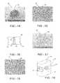
- FIG. 14is a SEM micrograph of the alternate filler material configuration shown in FIG. 12 ;
- FIG. 15is an optical micrograph of the alternate filler material configuration shown in FIG. 14 ;
- FIG. 16is a schematic representation of an alternate configuration of the filler material on the visible side of the panel.
- FIG. 17is a SEM micrograph of the alternate filler material configuration shown in FIG. 16 ;
- FIG. 18is an optical micrograph of the alternate filler material configuration shown in FIG. 17 ;
- FIG. 19is a schematic representation of a housing utilizing a light transmissive panel including filled vias.
- FIG. 19illustrates a product resulting from one of the methods.
- the disclosureutilizes via drilling techniques to create a micro via that is then filled with a light transmissive material. Via drilling is known in the unrelated field of electronics manufacturing. Vias are created in multi-layered interconnected substrates and lined with a conductor, such as copper, to permit an electrical connection between different layers in a circuit.
- FIG. 1A method 10 and steps for filling a via with light transmissive material are illustrated in FIG. 1 .
- a panel or substrate 12is provided.
- Panel 12 as shownis a relatively thin continuous sheet of material.
- Panel 12includes a first or back side 14 and an opposing second or front side 18 defining a panel thickness 20 .
- Front side 18is relatively smooth and substantially unbroken to the naked eye.
- Panel 12may be made from anodized aluminum or other materials known to those skilled in the art.
- the method 10includes drilling one or a plurality of micro-vias or holes 30 through the panel 12 .
- the vias 30are conical-shaped having sidewalls 34 and a first opening 40 in panel first side 14 and an opposing second opening 44 on panel side 18 .
- First via opening 40is larger in diameter than second via opening 44 .
- first via opening 40is approximately 90-100 micrometers ( ⁇ m) in diameter
- second via opening 44is approximately 30-40 micrometers ( ⁇ m) in diameter. It is understood that larger or smaller conical openings and other via shapes and configurations may be used.
- the vias shownare drilled or machined out of the panel using a laser 24 , such as a diode-pumped solid-state pulsed laser, in a circular or spiral pattern. It has been shown that a Nd:YAG 355 nm spot 22 with a pulse repetition rate of 30 kHz and ⁇ 60 nanosecond pulse width is useful in machining out the preferred conical-shaped vias 30 . Drilling of the exemplary vias 30 is accomplished from back side 14 through panel 12 toward the front side 18 . Other types of lasers with different characteristics and other machining processes from drilling vias known to those skilled in the art may be used to suit the particular application.
- the method 10optionally includes the step 46 of cleaning the drilled vias 30 to remove any debris or deposits formed during the machining process. It has been shown that a CO 2 snow jet cleaning and isopropyl are effective in cleaning the vias. Other via cleaning techniques known by those skilled in the art may also be used. For example, ultrasonic cleaning using, for example, ultrasonic baths may be used. Also, the application of high-pressure air, like the snow jet, may be made from a source movably located in a similar manner to the drill 24 to clean the vias.
- the method 10includes applying a filler material coating 50 into the vias 30 .
- the filler material 50may be a visible light transmissive material.
- filler material 50is an optically transparent ultraviolet (UV)-curable, acrylate polymer that is in a liquid phase at the time of application to panel 12 .
- UVultraviolet
- Other plastics or polymers with light transmissive propertiesmay also be used.
- the exemplary UV curable filler materialis substantially clear when cured.
- the filler material 50can be applied to the panel second side 18 over the top of the second, optionally smaller openings 44 , of vias 30 .
- the filler material 50flows into and through the vias 30 from the second side 18 to the first side 14 , effectively filling the vias 30 as best shown in FIGS. 1 , 8 and 9 .
- Excess filler material 50may propagate on panel 12 second side 18 (shown as 66 ) and first side 14 (shown as 62 ) as best seen in FIG. 1 .
- the filler material 50 as shownis applied with a syringe-type device 54 .
- Other filler material 50 application devices and techniques known by those skilled in the artmay be used. Examples include ink jet techniques and pad printing techniques.
- filler material 50may be applied to back side 14 so the filler material 50 flows through the via 30 from back side 14 toward front side 18 in a similar manner as described.
- method 10may include the step 76 of curing the exemplary liquid phase silica-based filler material 50 by exposing the filler 50 to UV light. Exposure to UV light 76 initiates free-radical polymerization of the silicate filler material 50 inside and through the vias 30 . In one method of applying the UV light, the UV light is applied to back side 14 and via 30 (i.e., the large openings 40 ) to promote curing of filler material 50 in the vias 30 . When cured, the exemplary filler material 50 is optically transparent permitting passage of visible light through the filler 50 and panel 12 through vias 30 .
- Method 10includes the step 82 of removing any excess or uncured filler material deposits 66 from the panel visible, front side 18 as shown in FIG. 1 .
- filler excess deposits 66may be removed from front side 18 through a simple isopropanol wipe, leaving a visibly smooth and clean surface.
- Other methods and techniques for removing excess deposits 66may be used.
- Method 10may optionally include the step 90 of exposing the filler material 50 in the vias 30 adjacent to the visible panel side 18 after the step of removing excess deposits 66 to assist curing of the filler material 50 throughout the vias 30 .
- the filler material 50 most adjacent to the panel visible surface 18may be slightly below front side 18 forming a recess 94 between the filler 50 and front side 18 .
- cured excess filler deposits 66may take a convex shape or form as opposed to being recessed into vias 30 as shown in FIG. 9 .
- FIGS. 10-12 and FIGS. 13-15illustrate two such convex forms for the cured excess filler deposits 66 .
- the convex shapeextends beyond and surrounds the second via opening 44 .
- the convex shapeis approximately limited to the area of the second via opening 44 .
- FIGS. 16-18illustrate, instead of a concave or convex shape, a flush fill, that is, an embodiment where the filler material 50 is flush with the surface of the second, or front, side 18 .
- FIG. 19illustrates a panel 12 including a back light 70 , which may be an LED, fluorescent or incandescent light, or other lighting devices. Panel 12 may be a section inserted into a housing or may be an integral section of the housing 72 as shown in FIG. 19 .
- the resultant panel 12can be used in all manner of applications including hand-held electronic devices, for example, MP3 players, computers, cellular phones, DVD players and the like.
- the disclosed method and resultant panelis applicable in virtually all applications where a visually continuous and uninterrupted panel surface is desired having the capability to produce illuminated messages, images or other perceptible characteristics for the user.
Landscapes
- Engineering & Computer Science (AREA)
- Health & Medical Sciences (AREA)
- Manufacturing & Machinery (AREA)
- Ophthalmology & Optometry (AREA)
- Mechanical Engineering (AREA)
Abstract
Description
Claims (17)
Priority Applications (10)
| Application Number | Priority Date | Filing Date | Title |
|---|---|---|---|
| US11/742,862US8394301B2 (en) | 2006-06-02 | 2007-05-01 | Process for forming panel with an optically transmissive portion and products related thereto |
| EP07795410AEP2024767A4 (en) | 2006-06-02 | 2007-05-24 | Process for optically transparent via filling |
| JP2009513225AJP5124568B2 (en) | 2006-06-02 | 2007-05-24 | Manufacturing method of panel having light transmitting portion and panel manufactured using the method |
| KR1020087032264AKR101435224B1 (en) | 2006-06-02 | 2007-05-24 | A method of forming a panel having a light transmitting portion and a method of forming a panel having a light transmitting portion |
| SG2011036860ASG172615A1 (en) | 2006-06-02 | 2007-05-24 | Process for optically transparent via filling |
| CN200780019844.9ACN101454700B (en) | 2006-06-02 | 2007-05-24 | Process for forming panel with optically transparent part and related products |
| PCT/US2007/012600WO2007142909A2 (en) | 2006-06-02 | 2007-05-24 | Process for optically transparent via filling |
| TW96119145ATWI471074B (en) | 2006-06-02 | 2007-05-29 | Process for forming panet with an optically transmissive portion and products related thereto |
| US13/797,891US9568167B2 (en) | 2006-06-02 | 2013-03-12 | Products with a patterned light-transmissive portion |
| US15/398,171US20170114982A1 (en) | 2006-06-02 | 2017-01-04 | Products with a patterned light-transmissive portion |
Applications Claiming Priority (3)
| Application Number | Priority Date | Filing Date | Title |
|---|---|---|---|
| US81038006P | 2006-06-02 | 2006-06-02 | |
| US81058006P | 2006-06-02 | 2006-06-02 | |
| US11/742,862US8394301B2 (en) | 2006-06-02 | 2007-05-01 | Process for forming panel with an optically transmissive portion and products related thereto |
Related Child Applications (1)
| Application Number | Title | Priority Date | Filing Date |
|---|---|---|---|
| US13/797,891DivisionUS9568167B2 (en) | 2006-06-02 | 2013-03-12 | Products with a patterned light-transmissive portion |
Publications (2)
| Publication Number | Publication Date |
|---|---|
| US20070291496A1 US20070291496A1 (en) | 2007-12-20 |
| US8394301B2true US8394301B2 (en) | 2013-03-12 |
Family
ID=38861347
Family Applications (1)
| Application Number | Title | Priority Date | Filing Date |
|---|---|---|---|
| US11/742,862Expired - Fee RelatedUS8394301B2 (en) | 2006-06-02 | 2007-05-01 | Process for forming panel with an optically transmissive portion and products related thereto |
Country Status (1)
| Country | Link |
|---|---|
| US (1) | US8394301B2 (en) |
Cited By (2)
| Publication number | Priority date | Publication date | Assignee | Title |
|---|---|---|---|---|
| US10821889B2 (en) | 2018-10-19 | 2020-11-03 | Shanghai Yanfeng Inqiao Automotive Trim Systems Co. Ltd. | Vehicle interior component |
| US12083953B2 (en) | 2018-10-19 | 2024-09-10 | Shanghai Yanfeng Jinqiao Automotive Trim Systems Co. Ltd. | Vehicle interior component |
Families Citing this family (16)
| Publication number | Priority date | Publication date | Assignee | Title |
|---|---|---|---|---|
| EP2024767A4 (en) | 2006-06-02 | 2010-08-04 | Electro Scient Ind Inc | Process for optically transparent via filling |
| US8481887B2 (en)* | 2007-05-03 | 2013-07-09 | Electro Scientific Industries, Inc. | Method for machining tapered micro holes |
| US7886437B2 (en)* | 2007-05-25 | 2011-02-15 | Electro Scientific Industries, Inc. | Process for forming an isolated electrically conductive contact through a metal package |
| US20090312859A1 (en)* | 2008-06-16 | 2009-12-17 | Electro Scientific Industries, Inc. | Modifying entry angles associated with circular tooling actions to improve throughput in part machining |
| US7943862B2 (en)* | 2008-08-20 | 2011-05-17 | Electro Scientific Industries, Inc. | Method and apparatus for optically transparent via filling |
| US20100078418A1 (en)* | 2008-09-26 | 2010-04-01 | Electro Scientific Industries, Inc. | Method of laser micro-machining stainless steel with high cosmetic quality |
| US9346130B2 (en) | 2008-12-17 | 2016-05-24 | Electro Scientific Industries, Inc. | Method for laser processing glass with a chamfered edge |
| US8524127B2 (en)* | 2010-03-26 | 2013-09-03 | Electro Scientific Industries, Inc. | Method of manufacturing a panel with occluded microholes |
| US9289858B2 (en) | 2011-12-20 | 2016-03-22 | Electro Scientific Industries, Inc. | Drilling holes with minimal taper in cured silicone |
| US10357850B2 (en) | 2012-09-24 | 2019-07-23 | Electro Scientific Industries, Inc. | Method and apparatus for machining a workpiece |
| US9828278B2 (en) | 2012-02-28 | 2017-11-28 | Electro Scientific Industries, Inc. | Method and apparatus for separation of strengthened glass and articles produced thereby |
| KR20140138134A (en) | 2012-02-28 | 2014-12-03 | 일렉트로 싸이언티픽 인더스트리이즈 인코포레이티드 | Method and apparatus for separation of strengthened glass and articles produced thereby |
| WO2013130608A1 (en) | 2012-02-29 | 2013-09-06 | Electro Scientific Industries, Inc. | Methods and apparatus for machining strengthened glass and articles produced thereby |
| US9776906B2 (en) | 2014-03-28 | 2017-10-03 | Electro Scientific Industries, Inc. | Laser machining strengthened glass |
| US10442720B2 (en)* | 2015-10-01 | 2019-10-15 | AGC Inc. | Method of forming hole in glass substrate by using pulsed laser, and method of producing glass substrate provided with hole |
| ES2971924T3 (en)* | 2021-08-24 | 2024-06-10 | Antolin Grupo Ing Sa | Wrapping to cover backlit interior parts of vehicles, procedure and installation for its manufacture |
Citations (20)
| Publication number | Priority date | Publication date | Assignee | Title |
|---|---|---|---|---|
| US3440388A (en)* | 1966-04-04 | 1969-04-22 | Monsanto Co | Method for machining with laser beam |
| JPH0289740U (en) | 1988-12-28 | 1990-07-17 | ||
| JPH0716778A (en) | 1993-07-06 | 1995-01-20 | Brother Ind Ltd | Laser processing method |
| JPH07201260A (en)* | 1993-12-29 | 1995-08-04 | Yamatake Honeywell Co Ltd | Method for forming display window of electronic switch |
| JPH07271309A (en) | 1994-04-01 | 1995-10-20 | Giichi Ishihara | Display plate |
| JPH08298043A (en) | 1995-04-27 | 1996-11-12 | Oki Electric Ind Co Ltd | Push button with translucent part and its manufacture |
| JPH11168281A (en) | 1997-12-02 | 1999-06-22 | Hitachi Aic Inc | Manufacture of thin multilayer printed wiring board |
| US6211485B1 (en)* | 1996-06-05 | 2001-04-03 | Larry W. Burgess | Blind via laser drilling system |
| US20020170891A1 (en) | 2001-03-22 | 2002-11-21 | Adrian Boyle | Laser machining system and method |
| JP2003248445A (en) | 2002-02-25 | 2003-09-05 | Casio Comput Co Ltd | Light transmissive metal member, light emitting device using the same, and electronic device |
| US20040032659A1 (en)* | 2000-07-18 | 2004-02-19 | Drinkwater John K | Difractive device |
| JP2004104079A (en) | 2002-07-15 | 2004-04-02 | Murata Mfg Co Ltd | Ceramic multilayer circuit and manufacturing method thereof |
| WO2004077388A1 (en) | 2003-02-27 | 2004-09-10 | Bang & Olufsen A/S | Magic panel |
| JP2005066687A (en) | 2003-08-28 | 2005-03-17 | National Institute Of Advanced Industrial & Technology | Fine ablation processing method of transparent material |
| WO2005110666A1 (en) | 2004-04-14 | 2005-11-24 | Electro Scientific Industries, Inc | Methods of drilling through-holes in homogeneous and non-homogeneous substrates |
| JP2006062431A (en) | 2004-08-25 | 2006-03-09 | Toyoda Gosei Co Ltd | Decorating device |
| TW200624238A (en) | 2004-11-22 | 2006-07-16 | Sumitomo Electric Industries | The professing method for resin-made film with micro through hole in resin film and a device and the micro structure with the same |
| TWI277830B (en) | 1999-01-28 | 2007-04-01 | Sumitomo Chemical Co | Resist composition |
| US7230278B2 (en)* | 2003-09-01 | 2007-06-12 | Kabushiki Kaisha Toshiba | Optoelectronic semiconductor device and light signal input/output device |
| US7968820B2 (en)* | 2006-06-02 | 2011-06-28 | Electro Scientific Industries, Inc. | Method of producing a panel having an area with light transmissivity |
- 2007
- 2007-05-01USUS11/742,862patent/US8394301B2/ennot_activeExpired - Fee Related
Patent Citations (21)
| Publication number | Priority date | Publication date | Assignee | Title |
|---|---|---|---|---|
| US3440388A (en)* | 1966-04-04 | 1969-04-22 | Monsanto Co | Method for machining with laser beam |
| JPH0289740U (en) | 1988-12-28 | 1990-07-17 | ||
| JPH0716778A (en) | 1993-07-06 | 1995-01-20 | Brother Ind Ltd | Laser processing method |
| JPH07201260A (en)* | 1993-12-29 | 1995-08-04 | Yamatake Honeywell Co Ltd | Method for forming display window of electronic switch |
| JPH07271309A (en) | 1994-04-01 | 1995-10-20 | Giichi Ishihara | Display plate |
| JPH08298043A (en) | 1995-04-27 | 1996-11-12 | Oki Electric Ind Co Ltd | Push button with translucent part and its manufacture |
| US6211485B1 (en)* | 1996-06-05 | 2001-04-03 | Larry W. Burgess | Blind via laser drilling system |
| JPH11168281A (en) | 1997-12-02 | 1999-06-22 | Hitachi Aic Inc | Manufacture of thin multilayer printed wiring board |
| TWI277830B (en) | 1999-01-28 | 2007-04-01 | Sumitomo Chemical Co | Resist composition |
| US20040032659A1 (en)* | 2000-07-18 | 2004-02-19 | Drinkwater John K | Difractive device |
| JP2005507318A (en) | 2001-03-22 | 2005-03-17 | エグシル テクノロジー リミテッド | Laser processing system and method |
| US20020170891A1 (en) | 2001-03-22 | 2002-11-21 | Adrian Boyle | Laser machining system and method |
| JP2003248445A (en) | 2002-02-25 | 2003-09-05 | Casio Comput Co Ltd | Light transmissive metal member, light emitting device using the same, and electronic device |
| JP2004104079A (en) | 2002-07-15 | 2004-04-02 | Murata Mfg Co Ltd | Ceramic multilayer circuit and manufacturing method thereof |
| WO2004077388A1 (en) | 2003-02-27 | 2004-09-10 | Bang & Olufsen A/S | Magic panel |
| JP2005066687A (en) | 2003-08-28 | 2005-03-17 | National Institute Of Advanced Industrial & Technology | Fine ablation processing method of transparent material |
| US7230278B2 (en)* | 2003-09-01 | 2007-06-12 | Kabushiki Kaisha Toshiba | Optoelectronic semiconductor device and light signal input/output device |
| WO2005110666A1 (en) | 2004-04-14 | 2005-11-24 | Electro Scientific Industries, Inc | Methods of drilling through-holes in homogeneous and non-homogeneous substrates |
| JP2006062431A (en) | 2004-08-25 | 2006-03-09 | Toyoda Gosei Co Ltd | Decorating device |
| TW200624238A (en) | 2004-11-22 | 2006-07-16 | Sumitomo Electric Industries | The professing method for resin-made film with micro through hole in resin film and a device and the micro structure with the same |
| US7968820B2 (en)* | 2006-06-02 | 2011-06-28 | Electro Scientific Industries, Inc. | Method of producing a panel having an area with light transmissivity |
Non-Patent Citations (1)
| Title |
|---|
| Taiwanese Intellectual Property Office, Taiwan Search Report a in corresponding Taiwan application No. 096119145, dated Nov. 12, 2012. |
Cited By (2)
| Publication number | Priority date | Publication date | Assignee | Title |
|---|---|---|---|---|
| US10821889B2 (en) | 2018-10-19 | 2020-11-03 | Shanghai Yanfeng Inqiao Automotive Trim Systems Co. Ltd. | Vehicle interior component |
| US12083953B2 (en) | 2018-10-19 | 2024-09-10 | Shanghai Yanfeng Jinqiao Automotive Trim Systems Co. Ltd. | Vehicle interior component |
Also Published As
| Publication number | Publication date |
|---|---|
| US20070291496A1 (en) | 2007-12-20 |
Similar Documents
| Publication | Publication Date | Title |
|---|---|---|
| US8394301B2 (en) | Process for forming panel with an optically transmissive portion and products related thereto | |
| US9568167B2 (en) | Products with a patterned light-transmissive portion | |
| US8450640B2 (en) | Panel with micro-hole pattern in a structurally thin portion | |
| WO2011119931A2 (en) | Method of manufacturing a panel with occluded microholes and products made thereby | |
| JP5814121B2 (en) | Improved method and apparatus for filling optically transparent vias | |
| JP2009539226A5 (en) | ||
| CN101454700B (en) | Process for forming panel with optically transparent part and related products | |
| CN108747039B (en) | Liquid crystal panel marking method | |
| CN105323986A (en) | Manufacturing method for multilayer wiring board | |
| WO2019121084A1 (en) | Method for producing an electronic assembly, electronic assembly, image-generating device, head-up display and vehicle comprising a head-up display | |
| US8288682B2 (en) | Forming micro-vias using a two stage laser drilling process | |
| Cheng | Laser-Patterned Quantum Dot Color Conversion Film for Full-Color Mini/Micro-LED Displays | |
| JP2019201140A (en) | Multilayer circuit board and method for manufacturing the same | |
| CN102131350A (en) | Circuit board and its manufacturing process | |
| TW200911056A (en) | Method for manufacturing hollowed printed circuit board |
Legal Events
| Date | Code | Title | Description |
|---|---|---|---|
| AS | Assignment | Owner name:ELECTRO SCIENTIFIC INDUSTRIES, INC., OREGON Free format text:ASSIGNMENT OF ASSIGNORS INTEREST;ASSIGNORS:NASHNER, MICHAEL S.;HOWERTON, JEFFREY;LU, WEIXIONG;SIGNING DATES FROM 20070919 TO 20070926;REEL/FRAME:026424/0985 | |
| STCF | Information on status: patent grant | Free format text:PATENTED CASE | |
| FPAY | Fee payment | Year of fee payment:4 | |
| AS | Assignment | Owner name:BARCLAYS BANK PLC, AS COLLATERAL AGENT, NEW YORK Free format text:PATENT SECURITY AGREEMENT (ABL);ASSIGNORS:ELECTRO SCIENTIFIC INDUSTRIES, INC.;MKS INSTRUMENTS, INC.;NEWPORT CORPORATION;REEL/FRAME:048211/0312 Effective date:20190201 Owner name:BARCLAYS BANK PLC, AS COLLATERAL AGENT, NEW YORK Free format text:PATENT SECURITY AGREEMENT (TERM LOAN);ASSIGNORS:ELECTRO SCIENTIFIC INDUSTRIES, INC.;MKS INSTRUMENTS, INC.;NEWPORT CORPORATION;REEL/FRAME:048211/0227 Effective date:20190201 | |
| FEPP | Fee payment procedure | Free format text:MAINTENANCE FEE REMINDER MAILED (ORIGINAL EVENT CODE: REM.); ENTITY STATUS OF PATENT OWNER: LARGE ENTITY | |
| AS | Assignment | Owner name:BARCLAYS BANK PLC, AS COLLATERAL AGENT, NEW YORK Free format text:CORRECTIVE ASSIGNMENT TO CORRECT THE REMOVE U.S. PATENT NO. 7,919,646 PREVIOUSLY RECORDED ON REEL 048211 FRAME 0227. ASSIGNOR(S) HEREBY CONFIRMS THE PATENT SECURITY AGREEMENT (TERM LOAN);ASSIGNORS:ELECTRO SCIENTIFIC INDUSTRIES, INC.;MKS INSTRUMENTS, INC.;NEWPORT CORPORATION;REEL/FRAME:055006/0492 Effective date:20190201 Owner name:BARCLAYS BANK PLC, AS COLLATERAL AGENT, NEW YORK Free format text:CORRECTIVE ASSIGNMENT TO CORRECT THE REMOVE U.S. PATENT NO.7,919,646 PREVIOUSLY RECORDED ON REEL 048211 FRAME 0312. ASSIGNOR(S) HEREBY CONFIRMS THE PATENT SECURITY AGREEMENT (ABL);ASSIGNORS:ELECTRO SCIENTIFIC INDUSTRIES, INC.;MKS INSTRUMENTS, INC.;NEWPORT CORPORATION;REEL/FRAME:055668/0687 Effective date:20190201 | |
| LAPS | Lapse for failure to pay maintenance fees | Free format text:PATENT EXPIRED FOR FAILURE TO PAY MAINTENANCE FEES (ORIGINAL EVENT CODE: EXP.); ENTITY STATUS OF PATENT OWNER: LARGE ENTITY | |
| STCH | Information on status: patent discontinuation | Free format text:PATENT EXPIRED DUE TO NONPAYMENT OF MAINTENANCE FEES UNDER 37 CFR 1.362 | |
| FP | Lapsed due to failure to pay maintenance fee | Effective date:20210312 | |
| AS | Assignment | Owner name:ELECTRO SCIENTIFIC INDUSTRIES, INC., OREGON Free format text:RELEASE BY SECURED PARTY;ASSIGNOR:BARCLAYS BANK PLC;REEL/FRAME:063009/0001 Effective date:20220817 Owner name:NEWPORT CORPORATION, MASSACHUSETTS Free format text:RELEASE BY SECURED PARTY;ASSIGNOR:BARCLAYS BANK PLC;REEL/FRAME:063009/0001 Effective date:20220817 Owner name:MKS INSTRUMENTS, INC., MASSACHUSETTS Free format text:RELEASE BY SECURED PARTY;ASSIGNOR:BARCLAYS BANK PLC;REEL/FRAME:063009/0001 Effective date:20220817 Owner name:ELECTRO SCIENTIFIC INDUSTRIES, INC., OREGON Free format text:RELEASE BY SECURED PARTY;ASSIGNOR:BARCLAYS BANK PLC;REEL/FRAME:062739/0001 Effective date:20220817 Owner name:NEWPORT CORPORATION, MASSACHUSETTS Free format text:RELEASE BY SECURED PARTY;ASSIGNOR:BARCLAYS BANK PLC;REEL/FRAME:062739/0001 Effective date:20220817 Owner name:MKS INSTRUMENTS, INC., MASSACHUSETTS Free format text:RELEASE BY SECURED PARTY;ASSIGNOR:BARCLAYS BANK PLC;REEL/FRAME:062739/0001 Effective date:20220817 |