US8392689B1 - Address optimized buffer transfer requests - Google Patents
Address optimized buffer transfer requestsDownload PDFInfo
- Publication number
- US8392689B1 US8392689B1US12/786,391US78639110AUS8392689B1US 8392689 B1US8392689 B1US 8392689B1US 78639110 AUS78639110 AUS 78639110AUS 8392689 B1US8392689 B1US 8392689B1
- Authority
- US
- United States
- Prior art keywords
- buffer
- data
- bank
- burst
- data burst
- Prior art date
- Legal status (The legal status is an assumption and is not a legal conclusion. Google has not performed a legal analysis and makes no representation as to the accuracy of the status listed.)
- Expired - Fee Related, expires
Links
Images


Classifications
- G—PHYSICS
- G06—COMPUTING OR CALCULATING; COUNTING
- G06F—ELECTRIC DIGITAL DATA PROCESSING
- G06F3/00—Input arrangements for transferring data to be processed into a form capable of being handled by the computer; Output arrangements for transferring data from processing unit to output unit, e.g. interface arrangements
- G06F3/06—Digital input from, or digital output to, record carriers, e.g. RAID, emulated record carriers or networked record carriers
- G06F3/0601—Interfaces specially adapted for storage systems
- G06F3/0602—Interfaces specially adapted for storage systems specifically adapted to achieve a particular effect
- G06F3/061—Improving I/O performance
- G06F3/0613—Improving I/O performance in relation to throughput
- G—PHYSICS
- G06—COMPUTING OR CALCULATING; COUNTING
- G06F—ELECTRIC DIGITAL DATA PROCESSING
- G06F3/00—Input arrangements for transferring data to be processed into a form capable of being handled by the computer; Output arrangements for transferring data from processing unit to output unit, e.g. interface arrangements
- G06F3/06—Digital input from, or digital output to, record carriers, e.g. RAID, emulated record carriers or networked record carriers
- G06F3/0601—Interfaces specially adapted for storage systems
- G06F3/0628—Interfaces specially adapted for storage systems making use of a particular technique
- G06F3/0655—Vertical data movement, i.e. input-output transfer; data movement between one or more hosts and one or more storage devices
- G06F3/0656—Data buffering arrangements
- G—PHYSICS
- G06—COMPUTING OR CALCULATING; COUNTING
- G06F—ELECTRIC DIGITAL DATA PROCESSING
- G06F3/00—Input arrangements for transferring data to be processed into a form capable of being handled by the computer; Output arrangements for transferring data from processing unit to output unit, e.g. interface arrangements
- G06F3/06—Digital input from, or digital output to, record carriers, e.g. RAID, emulated record carriers or networked record carriers
- G06F3/0601—Interfaces specially adapted for storage systems
- G06F3/0668—Interfaces specially adapted for storage systems adopting a particular infrastructure
- G06F3/0671—In-line storage system
- G06F3/0673—Single storage device
- G06F3/0674—Disk device
- G06F3/0676—Magnetic disk device
- G—PHYSICS
- G06—COMPUTING OR CALCULATING; COUNTING
- G06F—ELECTRIC DIGITAL DATA PROCESSING
- G06F3/00—Input arrangements for transferring data to be processed into a form capable of being handled by the computer; Output arrangements for transferring data from processing unit to output unit, e.g. interface arrangements
- G06F3/06—Digital input from, or digital output to, record carriers, e.g. RAID, emulated record carriers or networked record carriers
- G06F3/0601—Interfaces specially adapted for storage systems
- G06F3/0668—Interfaces specially adapted for storage systems adopting a particular infrastructure
- G06F3/0671—In-line storage system
- G06F3/0673—Single storage device
- G06F3/0679—Non-volatile semiconductor memory device, e.g. flash memory, one time programmable memory [OTP]
Definitions
- Data storage devicesare commonly used to store data in computers, data bases, digital video recorders, and other devices.
- a data storage devicemay comprise a storage media, such as a hard disk and/or solid state memory, and a buffer for temporarily storing data to be written to the storage media and/or read from the storage media. It is desirable to arrange the transfer of data to and/or from the buffer in way that optimizes the data throughput of the buffer.
- FIG. 1is a block diagram of a data storage device according to an embodiment of the present invention.
- FIG. 2shows an example of a buffer client that accesses a buffer through a buffer manager according to an embodiment of the present invention
- FIG. 3Ashows an example of an first data burst according to an embodiment of the present invention
- FIG. 3Bshows an example of a middle data burst according to an embodiment of the present invention
- FIG. 3Cshows an example of a last data burst according to an embodiment of the present invention
- FIG. 4is a flow diagram of a method for writing data to a buffer according to an embodiment of the present invention.
- FIG. 5is a flow diagram of a method for reading data from a buffer according to an embodiment of the present invention.
- FIG. 6shows another example of a buffer client that accesses the buffer through the buffer manager according to another embodiment of the present invention.
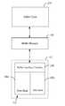
- FIG. 1shows a data storage device 110 according to an embodiment of the present invention.
- the data storage device 110includes a storage media 125 , which may comprise a hard disk, solid state memory (e.g., flash memory), or other type of memory.
- the data storage device 110also includes a host interface 115 , a buffer 132 , a buffer manager 130 , a storage media interface 120 , and a microprocessor 112 .
- the host interface 115interfaces the data storage device 110 to a host device (e.g., a host processor).
- the storage media interface 120reads data from and writes data to the storage media 125 .
- the storage media interface 120may include a read/write head to magnetically read data from and write data to the hard disk.
- the buffer 132may be used to temporarily store data in the data storage device 110 , as discussed further below.
- the microprocessor 112may control operations of the data storage device 110 to execute read/write commands from the host device. For a host read command, the microprocessor 112 may instruct the storage media interface 120 to retrieve data from the storage media 125 requested by the host read command and store the data in the buffer 132 . The microprocessor 112 may then instruct the host device interface 115 to retrieve the data from the buffer 132 and send the data to the host device. For a host write command, the microprocessor 112 may instruct the host interface 115 to store the data from the host device in the buffer 130 and instruct the storage media interface 120 to retrieve the data from the buffer 132 and write the data to the storage media 125 . The microprocessor 112 may also manage at which buffer addresses data is stored in the buffer 132 based on a buffer management scheme.
- the data storage device 110may also include a data manipulation engine 150 configured to perform data manipulation operations (e.g., logic operations) on data in the data storage device 110 .
- data manipulation operationse.g., logic operations
- the microprocessor 112may instruct the data manipulation engine 150 to retrieve data from the buffer 132 , perform a data manipulation operation on the data, and store the resultant data in the buffer 132 .
- the buffer 132may comprise dynamic random access memory (DRAM), synchronous DRAM (SDRAM), double data rate (DDR) SDRAM, and/or other type of memory.
- the buffer manager 130manages the flow of data between the buffer 132 and various buffer clients in the data storage device 110 that access the buffer 132 .
- the buffer clientsmay include the storage media interface 120 , the data manipulation engine 150 , and the host interface 115 . If multiple buffer clients attempt to access the buffer 132 , then the buffer manager 130 may manage access to the buffer 132 among the different buffer clients.
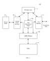
- FIG. 2shows an example of a buffer client 250 that accesses the buffer 132 through the buffer manager 130 according to an embodiment of the present invention.
- the buffer client 250may include the storage media interface 120 , the data manipulation engine 150 , the host interface 115 or other component in the data storage device 110 that accesses the buffer 132 .
- FIG. 2shows one buffer client 250 that is shown in FIG. 2 for ease of discussion, one skilled in the art will appreciate that the data storage device 110 may include multiple buffer clients that access the buffer 132 through the buffer manager 130 .
- the buffer 132comprises buffer interface circuitry 230 and memory 235 for storing data.
- the buffer interface circuitry 230receives write/read buffer commands from the buffer manager 130 and writes data to and/or reads data from the memory 235 based on the buffer commands.
- the memory 235comprises an even bank 240 a and an odd bank 240 b . Although two banks are shown in FIG. 2 , those skilled in the art will appreciate that the buffer 132 may include any number of even and odd banks.
- the buffer interface circuitry 230may alternately transfer data to the even and odd banks 240 a and 240 b and/or alternately transfer data from the even and odd banks 240 a and 240 b .
- the buffer interface circuitry 230may transfer data to or from one of the banks 240 a and 240 b while precharging the other bank 240 a and 240 b to prepare the other bank 240 a and 240 b for the next data transfer.
- Precharging a bank 240 a and 240 bmay involve precharging sense amplifiers and/or other circuitry used for transferring data to or from the bank.
- An advantage of this embodimentis that it hides latencies associated with precharging the banks 240 a and 240 b . This is because, while one bank 240 a and 240 b is precharging, data is being transferred to or from the other bank 240 a and 240 b . As a result, the effective buffer throughput is increased.
- a sequence of buffer addresses in the buffer 132may be allocated between the even and odd banks 240 a and 240 b such that alternating portions of the buffer address sequence are located in the even and odd banks 240 a and 240 b .
- a first portion of the buffer address sequencemay be in the even bank 240 a and a second portion of the buffer address sequence adjacent to the first portion may be in the odd bank 240 b , where each portion spans one bank length (e.g., 32 DWords, where each DWord is 4 bytes or 32 bits).
- Each buffer addressmay hold one DWord.
- a buffer address located at an even or odd bank boundarymay be referred to as a bank boundary address. For the example where one bank length is 32 DWords, a bank boundary address may occur every 32 DWords.
- the buffer manager 130may optimize the transfer of a data sequence to or from the buffer 132 by sending overlapping buffer commands to the buffer 132 .
- the buffer interface circuitry 235may transfer a first portion of the data sequence spanning one bank length to or from the even bank 240 a in response to a first one of the overlapping buffer commands while precharging the odd bank 240 b in response to a second one of the overlapping buffer commands. The precharging prepares the odd bank 240 b for the transfer of a second portion of the data sequence spanning one bank length.
- the odd buffer 240 bis ready for the buffer interface circuitry 235 to transfer the second portion of the data sequence to or from the odd bank 240 b .
- the overlapping buffer commandsallows the buffer manager 130 to transfer data to or from one of the even and odd banks 240 a and 240 b while the other bank is being precharged, thereby optimizing buffer throughput.
- the buffer client 250may send a plurality of transfer requests to the buffer manager 130 , where each transfer request requests the transfer of a portion of the data from the buffer client 250 to the buffer manager 130 in a data burst.
- the buffer manager 130may send a signal to the buffer client 250 indicating that it is ready to receive the data burst corresponding to the request.
- the buffer client 250may then transfer the data burst to the buffer manager 130 .
- the buffer manager 130may send one or more buffer commands to the buffer 132 to write the received data burst to the buffer 132 .
- the buffer manager 130may also receive transfer requests from other buffer clients in the data storage device 110 and determine in which order to service the requests. For example, the buffer manager 130 may group transfer requests in the same direction together to minimize the change in direction of data transfers.
- the buffer client 250may transfer a data burst to the buffer manager 130 , in which the data burst spans two bank lengths (e.g., 64 DWords) and is aligned with an even bank boundary. This allows the buffer manager 130 to transfer the received data burst to the even and odd banks 240 a and 240 b of the buffer 132 using overlapping buffer commands as discussed above.
- two bank lengthse.g. 64 DWords
- the buffer client 250may send a plurality of transfer requests to the buffer manager 130 , where each transfer request requests a portion of the data from the buffer manager 130 in a data burst.
- the buffer manager 130may read the data burst corresponding to the request from the buffer 132 and transfer the read data burst to the buffer client 250 . This processes may be repeated until all of the data is transferred to the buffer client 250 .
- the buffer manager 130may transfer a data burst to the buffer client 250 , in which the data burst spans two bank lengths (e.g., 64 DWords) and is aligned with an even bank boundary. This allows the buffer manager 130 to read the data burst from the even and odd banks 240 a and 240 b of the buffer 132 using overlapping buffer commands as discussed above.
- two bank lengthse.g. 64 DWords
- the data that the client buffer 250 needs to transfer to or from the buffer 132may not be aligned with an even bank boundary.
- the microprocessor 112may instruct the host interface 115 to transfer data to and/or from the buffer 132 starting at a buffer address that is not aligned with an even bank boundary. This may be due to the fact that data is sent to and/or received from the host device in sectors, in which the sector size is not an integer multiple of two bank lengths.
- the client buffer 250is configured to transfer data to and/or from the buffer manager 130 in data bursts that optimize buffer throughput even when the starting buffer address for the data is not aligned with an even bank boundary.
- the client buffer 250determines a first data burst for transferring a first portion of the data to or from the buffer 132 through the buffer manager 130 .
- the client buffer 250computes the length of the first data burst as the difference between the starting buffer address for the data and the next even bank boundary address. This ensures that the next data burst is aligned with an even bank boundary, as discussed further below.
- the client buffer 250then sends a transfer request to the buffer manager 130 to transfer the first portion of the data in the first data burst.
- FIG. 3AAn example of the first data burst is shown in FIG. 3A , in which the first data burst starts at a buffer address that is not aligned with an even bank boundary and ends at an odd bank boundary.
- the first data bursthas a length equal to the difference between the starting buffer address and the next even bank boundary.
- the length of the first data burstmay be given in units of DWords.
- the client buffer 250determines one or more middle data bursts for transferring subsequent portions of the data to or from the buffer 132 through the buffer manager 130 .
- a middle data burstmay refer to a data burst that is between the first data burst and a last data burst, discussed below.
- each middle data burstmay have a length equal to an integer multiple of two bank lengths and be aligned with an even bank boundary. This allows the buffer manager 130 to transfer each middle data burst to or from the buffer 132 using overlapping buffer commands to optimize buffer throughput.
- the client buffer 250may send a transfer request to the buffer manager 130 to transfer the middle data burst.
- middle data burstAn example of a middle data burst is shown in FIG. 3B , in which the middle data burst starts at an even bank boundary and ends at an odd bank boundary, and has a length of two data bursts.
- the middle data burstmay have a length of 64 DWords.
- the buffer client 250determines the last data burst to transfer the remaining data to or from the buffer 132 through the buffer manager 130 .
- the last data bursthas a length equal to the amount of data remaining to be transferred and is aligned with an even bank boundary.
- the last data burstmay or may not end at an odd bank boundary.
- the client buffer 250may send a transfer request to the buffer manager 130 to transfer the last data burst.
- FIG. 3CAn example of the last data burst is shown in FIG. 3C , in which the final data burst starts at an even bank boundary and ends at a buffer address that is not aligned with an odd bank boundary.
- the length of the last data burstis equal to the amount of data remaining to be transferred.
- the buffer client 250advantageously optimizes buffer throughput even when the starting buffer address of the data to be transferred to and/or from the buffer 132 is not aligned with an even bank boundary. This is because the first data burst aligns the next data burst with an even bank boundary. As a result, each of the middle data bursts can be aligned with an even bank boundary and have a length of two bank lengths. This allows the buffer manager 130 to transfer the middle data bursts to and/or from the buffer 132 using overlapping buffer commands to optimize buffer throughput.
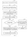
- FIG. 4is a flow diagram of a method for writing data from the buffer client 250 to the buffer 132 according to an embodiment of the present invention.
- step 410an operation to transfer data to the buffer 132 is initiated.
- the datamay be a data sequence to be written to sequential buffer addresses in the buffer 132 starting at a buffer address that is not aligned with a bank boundary.
- step 420the difference between a buffer boundary address and the starting buffer address for the data is computed.
- the buffer boundary addressmay be aligned with an even bank boundary.
- a first data burstis generated having a length equal to the computed difference and including a first portion of the data to be written to the buffer 132 .
- the first data burstis written to the buffer 132 .
- Thismay involve the buffer client 250 sending a transfer request to the buffer manager 130 for the first data burst and the buffer client 250 transferring the first data burst to the buffer manager 130 when the buffer manager 130 is ready to receive the first data burst.
- the buffer manager 130may then write the first data burst to the buffer 132 .
- step 450a determination is made whether the remaining data to be transferred exceeds two bank lengths. If the remaining exceeds two bank lengths, then the method proceeds to step 460 . Otherwise, the method proceeds to step 480 .
- a middle data burstis generated having a length equal to an integer multiple of two bank lengths and including a portion of the remaining data to be written to the buffer 130 .
- the middle data burstmay be aligned with an even bank boundary.
- step 470the middle data burst is written to the buffer 132 .
- Thismay involve the buffer client 250 sending a transfer request to the buffer manager 130 for the middle data burst and the buffer client 250 transferring the middle data burst to the buffer manager 130 when the buffer manager 130 is ready to receive the middle data burst.
- the buffer manager 130may then write the middle data burst to the buffer 132 using overlapping buffer command to optimize buffer throughput.
- step 470the method proceeds back to step 450 .
- a last data burstis generated having a length equal to the remaining data to be written to the buffer 130 and including the remaining data.
- the last data burstis written to the buffer 132 . This may involve the buffer client 250 sending a transfer request to the buffer manager 130 for the last data burst and the buffer client 250 transferring the last data burst to the buffer manager 130 when the buffer manager 130 is ready to receive the last data burst. The buffer manager 130 may then write the last data burst to the buffer 132 .
- FIG. 5is a flow diagram of a method for reading data from the buffer 132 to the buffer client 250 according to an embodiment of the present invention.
- step 510an operation to transfer data from the buffer 132 is initiated.
- the datamay be a data sequence that is stored in sequential buffer addresses in the buffer 132 starting at a buffer address that is not aligned with a bank boundary.
- step 520the difference between a buffer boundary address and the starting buffer address for the data is computed.
- the buffer boundary addressmay be aligned with an even bank boundary.
- a first data burstis determined having a length equal to the computed difference and including a first portion of the data to be read from the buffer 132 .
- the first data burstis read the buffer 132 .
- Thismay involve the buffer client 250 sending a transfer request to the buffer manager 130 for the first data burst.
- the buffer manager 130services the request by reading the first data burst from the buffer 132 and transferring the first data burst to the buffer client 250 .
- step 550a determination is made whether the remaining data to be transferred exceeds two bank lengths. If the remaining exceeds two bank lengths, then the method proceeds to step 560 . Otherwise, the method proceeds to step 580 .
- a middle data burstis determined having a length equal to a multiple integer of two bank lengths and including a portion of the remaining data to be read from the buffer 130 .
- the middle data burstmay be aligned with an even bank boundary.
- step 570the middle data burst is read from the buffer 132 .
- Thismay involve the buffer client 250 sending a transfer request to the buffer manager 130 for the middle data burst.
- the buffer manager 130services the request by reading the middle burst from the buffer 132 and transferring the middle data burst to the buffer client 250 . Since the middle data burst is aligned with an even bank boundary and is a multiple integer of two bank lengths, the buffer manager 130 can read the middle data burst from the buffer 132 using overlapping buffer commands.
- step 570the method proceeds back to step 550 .
- a last data burstis determined having a length equal to the remaining data to be read from the buffer 130 and including the remaining data.
- the last data burstis read from the buffer 132 . This may involve the buffer client 250 sending a transfer request to the buffer manager 130 for the last data burst. The buffer manager 130 services the request by reading the last data burst from the buffer 132 and transferring the last data burst to the buffer client 250 .
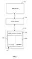
- FIG. 6shows the buffer client 250 according to an embodiment of the present invention.
- the buffer client 250may be used to implement the host interface 115 or the storage media interface 120 shown in FIG. 1 .
- the buffer client 250includes an interface 610 , a command processor 618 , a transfer engine 620 and a first-in first-out memory (FIFO) 615 .
- the interface 610is configured to receive data from and/or send data to the host device or the storage media 125 .
- the FIFO 615is configured to temporarily store data to be transferred to the buffer manager 130 and/or data received from the buffer manager 130 .
- the command processor 618is configured to instruct the transfer engine 620 to transfer data to and/or from the buffer 132 through the buffer manager 130 based on a host transfer command or a storage media transfer command, as discussed further below. Some or all of the functions of the command processor 618 may be performed by the microprocessor 112 .
- the command processor 618initiates a data transfer operation based on a host transfer command or a storage media transfer command.
- the host transfer commandmay be issued by the microprocessor 112 to write data received from the host device to the buffer 132 .
- a storage media transfer commandmay be issued by the microprocessor 112 to write data read from the storage media 125 to the buffer 132 .
- the command processor 618may send information to the transfer engine 620 to perform the data transfer operation including the transfer direction, the starting buffer address and/or the amount of data to be transferred.
- the transfer directionis towards the buffer 132 .
- the transfer engine 620may perform the transfer operation as data is received in the FIFO 615 from the host device or the storage media 125 . To begin the transfer operation, the transfer engine 620 may send the starting buffer address to the buffer manager 130 .
- the transfer engine 620may then compute the difference between the starting buffer address and an even bank boundary address, and use the computed difference as the length for the first data burst.
- the transfer engine 620may also set an internal flag indicating that the upcoming data burst is the first data burst and the computed difference should be used for the length of the data burst.
- the transfer engine 620may then monitor the amount of data in the FIFO 615 as the FIFO 615 receives data from the host device or storage media 125 . When there is enough data in the FIFO 615 to transfer the first data burst, the transfer engine 620 may send a transfer request to the buffer manager 130 for the first data burst. The buffer manager 130 may send a data strobe to the transfer engine 620 when the buffer manager 130 is ready to receive the first data burst from the buffer client 250 and send an acknowledge to the transfer engine 620 when the first data burst has been captured. At this time, the internal flag indicating the first data burst condition may be cleared.
- the buffer manager 130may then write the first data burst to the buffer 132 starting at the starting buffer address. For the example where the data is written to sequential buffer addresses, the buffer manager 130 may maintain a local buffer address indicating the next buffer address to be written. In this example, the buffer manager 130 may initialize the local buffer address at the starting buffer address and increment the local buffer address as data is written to the buffer 132 .
- the transfer engine 620may then generate a middle data burst to transfer a subsequent portion of the data to be written to the buffer 132 .
- the middle data burstmay be an integer multiple of two banks lengths in length.
- the transfer engine 620may monitor the amount of data in the FIFO 615 and send a transfer request to the buffer manager 130 when there is enough data in the FIFO 615 to transfer a middle data burst spanning two bank lengths.
- the amount of data in the FIFO 615may increase while the transfer engine 620 is waiting to be serviced by the buffer manager 130 . If the amount of data increases to the next multiple of two bank lengths, then a burst count indicating the length of the middle burst is updated to reflect the new transfer length. This allows the burst count to be updated until an acknowledgement is asserted by the buffer manager 130 .
- the burst countmay be sent to the buffer manager 130 to indicate the transfer length for the middle data burst.
- the transfer engine 620transfers the middle data burst to the buffer manager 130 .
- the buffer manager 130may then write the middle data burst to the buffer 132 using overlapping buffer commands to optimize buffer throughput.
- the process of transferring middle data burstsmay be repeated until the remaining data to be written to the buffer 132 is equal to or less then two bank lengths.
- the transfer engine 620may send a request to the buffer manager 130 to transfer the last data burst.
- the transfer engine 620transfers the last data burst to the buffer manager 130 , and the buffer manager 130 writes the data burst to the buffer 132 .
- the command processor 618initiates a data transfer operation based on a host transfer command or a storage media transfer command.
- the host transfer commandmay be issued by the microprocessor 112 to read data from the buffer 132 and send the data to the host device.
- the command processor 618may send information to the transfer engine 620 to perform the data transfer operation including the transfer direction, the starting buffer address and/or the amount of data to be transferred.
- the transfer directionis towards the buffer client 250 .
- the transfer engine 620may send the starting buffer address to the buffer manager 130 .
- the transfer engine 620may then compute the difference between the starting buffer address and an even bank boundary address, and use the computed difference as the length for the first data burst.
- the transfer engine 620may also set an internal flag indicating that the upcoming data burst is the first data burst and the computed difference should be used for the length of the data burst.
- the transfer engine 620may send a transfer request to the buffer manager 130 for the first data burst.
- the buffer manager 130may read the first data burst from the buffer 132 .
- the buffer manager 130may then may send a data strobe to the transfer engine 620 when the buffer manager 130 is ready to transfer the first data burst to the buffer client 250 .
- the internal flag indicating the first data burst conditionmay be cleared.
- the buffer manager 130may maintain a local buffer address indicating the next buffer address to be read. In this example, the buffer manager 130 may initialize the local buffer address at the starting buffer address and increment the local buffer address as data is read from the buffer 132 .
- the transfer engine 620may then determine a middle data burst to transfer a subsequent portion of the data to be read from the buffer 132 .
- the middle data burstmay be an integer multiple of two banks lengths in length.
- the transfer engine 620may monitor the amount of space available in the FIFO 615 as data in the FIFO is sent to the host device or storage media 125 .
- the transfer engine 620may then send a transfer request to the buffer manager 130 when there is enough space in the FIFO 615 to receive a middle data burst spanning two bank lengths.
- the amount of available space in the FIFO 615may increase while the transfer engine 520 is waiting to be serviced by the buffer manager 130 . If the available space increases to the next multiple of two bank lengths, then a burst count indicating the length of the middle burst is updated to reflect the new transfer length.
- the buffer manager 130may read the middle data burst from the buffer 132 and transfer the middle burst to the buffer client 250 .
- the process of transferring middle data burstsmay be repeated until the remaining data to be read from the buffer 132 is equal to or less then two bank lengths.
- the transfer engine 620may send a request to the buffer manager 130 for the last data burst.
- the buffer manager 130may read the last data burst from the buffer 132 and transfer the last data burst to the buffer client 250 .
- the transfer engine 620may compare the computed difference to the amount of data that needs to be transferred to or from the buffer 132 . If the amount of data is less than the computed difference, then the transfer engine 620 may transfer the data in one data burst having a length equal to the amount of data to be transferred. If the amount of data exceeds the computed difference, then the transfer engine 610 may transfer the data as discussed above.
- the data to be transferred to or from the buffer 132may comprise one or more sectors.
- each sectormay correspond to a logical block address used by the host device to address data stored in the data storage device 110 .
- the command processor 618may send the transfer engine 620 the number of sectors in the data to be transferred and the sector size.
- the transfer engine 620may sequentially transfer the sectors to or from the buffer 132 , in which the first data burst is used to transfer a first portion of the sector sequence, one or more middle data bursts are used to transfer subsequent portions of the sector sequence, and the last data burst is used to transfer a remaining portion of the sector sequence.
- a middle data burstmay include a remaining portion of one sector and a beginning portion of the next sector in the sector sequence.
- the transfer engine 620may transfer the next portion of the sector sequence using a data burst having a length equal to the difference between the next buffer address and an even bank boundary. This re-establishes alignment of the subsequent data burst to an even bank boundary.
Landscapes
- Engineering & Computer Science (AREA)
- Theoretical Computer Science (AREA)
- Human Computer Interaction (AREA)
- Physics & Mathematics (AREA)
- General Engineering & Computer Science (AREA)
- General Physics & Mathematics (AREA)
- Information Transfer Systems (AREA)
Abstract
Description
Claims (18)
Priority Applications (1)
| Application Number | Priority Date | Filing Date | Title |
|---|---|---|---|
| US12/786,391US8392689B1 (en) | 2010-05-24 | 2010-05-24 | Address optimized buffer transfer requests |
Applications Claiming Priority (1)
| Application Number | Priority Date | Filing Date | Title |
|---|---|---|---|
| US12/786,391US8392689B1 (en) | 2010-05-24 | 2010-05-24 | Address optimized buffer transfer requests |
Publications (1)
| Publication Number | Publication Date |
|---|---|
| US8392689B1true US8392689B1 (en) | 2013-03-05 |
Family
ID=47749164
Family Applications (1)
| Application Number | Title | Priority Date | Filing Date |
|---|---|---|---|
| US12/786,391Expired - Fee RelatedUS8392689B1 (en) | 2010-05-24 | 2010-05-24 | Address optimized buffer transfer requests |
Country Status (1)
| Country | Link |
|---|---|
| US (1) | US8392689B1 (en) |
Cited By (126)
| Publication number | Priority date | Publication date | Assignee | Title |
|---|---|---|---|---|
| US8879188B1 (en) | 2010-08-23 | 2014-11-04 | Western Digital Technologies, Inc. | Disk drive employing fly height calibration tracks to account for magnetic entropy and thermal decay |
| US8891193B1 (en) | 2013-05-09 | 2014-11-18 | Western Digital Technologies, Inc. | Disk drive calibrating threshold and gain of touchdown sensor |
| US8891341B1 (en) | 2013-03-11 | 2014-11-18 | Western Digital Technologies, Inc. | Energy assisted magnetic recording disk drive using modulated laser light |
| US8902529B1 (en) | 2012-11-20 | 2014-12-02 | Western Digital Technologies, Inc. | Dual frequency crystal oscillator |
| US8902527B1 (en) | 2010-03-22 | 2014-12-02 | Western Digital Technologies, Inc. | Systems and methods for improving sequential data rate performance using sorted data zones |
| US8908311B1 (en) | 2014-01-27 | 2014-12-09 | Western Digital Technologies, Inc. | Data storage device writing a multi-sector codeword in segments over multiple disk revolutions |
| US8909889B1 (en) | 2011-10-10 | 2014-12-09 | Western Digital Technologies, Inc. | Method and apparatus for servicing host commands by a disk drive |
| US8914625B1 (en) | 2009-07-31 | 2014-12-16 | Western Digital Technologies, Inc. | Automatically configuring a web browser file when booting an operating system from a data storage device |
| US8922939B1 (en) | 2013-04-02 | 2014-12-30 | Western Digital Technologies, Inc. | Disk drive generating feed-forward fly height control based on temperature sensitive fly height sensor |
| US8937782B1 (en) | 2012-05-07 | 2015-01-20 | Western Digital Technologies, Inc. | Hard disk drive assembly including a NVSM to store configuration data for controlling disk drive operations |
| US8941941B1 (en) | 2013-02-28 | 2015-01-27 | Western Digital Technologies, Inc. | Disk drive calibrating touchdown sensor |
| US8949521B1 (en) | 2013-04-10 | 2015-02-03 | Western Digital Technologies, Inc. | Actuator prepositioning for disk drive |
| US8947812B1 (en) | 2014-03-27 | 2015-02-03 | Western Digital Technologies, Inc. | Data storage device comprising equalizer filter and inter-track interference filter |
| US8953277B1 (en) | 2014-06-16 | 2015-02-10 | Western Digital Technologies, Inc. | Data storage device writing tracks on a disk with equal spacing |
| US8953269B1 (en) | 2014-07-18 | 2015-02-10 | Western Digital Technologies, Inc. | Management of data objects in a data object zone |
| US8954664B1 (en) | 2010-10-01 | 2015-02-10 | Western Digital Technologies, Inc. | Writing metadata files on a disk |
| US8959281B1 (en) | 2012-11-09 | 2015-02-17 | Western Digital Technologies, Inc. | Data management for a storage device |
| US8958167B1 (en) | 2013-12-23 | 2015-02-17 | Western Digital Technologies, Inc. | Detection of disk surface irregularities in data storage devices |
| US8970978B1 (en) | 2012-10-22 | 2015-03-03 | Western Digital Technologies, Inc. | Disk drive detecting head touchdown by applying DC+AC control signal to fly height actuator |
| US8976633B1 (en) | 2014-04-15 | 2015-03-10 | Western Digital Technologies, Inc. | Data storage device calibrating fly height actuator based on laser power for heat assisted magnetic recording |
| US8990493B1 (en) | 2011-06-30 | 2015-03-24 | Western Digital Technologies, Inc. | Method and apparatus for performing force unit access writes on a disk |
| US8988809B1 (en) | 2014-02-18 | 2015-03-24 | Western Digital (Fremont), Llc | Disk recording device for writing a radially coherent reference band by measuring relative timing offsets of reference bursts |
| US8988810B1 (en) | 2014-04-16 | 2015-03-24 | Western Digital Technologies, Inc. | Track measurement for data storage device |
| US8996839B1 (en) | 2012-01-23 | 2015-03-31 | Western Digital Technologies, Inc. | Data storage device aligning partition to boundary of sector when partition offset correlates with offset of write commands |
| US9001453B1 (en) | 2014-07-18 | 2015-04-07 | Western Digital Technologies, Inc. | Data storage device calibrating fly height actuator based on read mode touchdown resistance of touchdown sensor |
| US9009358B1 (en) | 2008-09-23 | 2015-04-14 | Western Digital Technologies, Inc. | Configuring a data storage device with a parameter file interlocked with configuration code |
| US9013818B1 (en) | 2013-12-06 | 2015-04-21 | Western Digital Technologies, Inc. | Disk drive measuring reader/writer gap by measuring fractional clock cycle over disk radius |
| US9013821B1 (en) | 2014-06-10 | 2015-04-21 | Western Digital Technologies, Inc. | Data storage device employing one-dimensional and two-dimensional channels |
| US9021410B1 (en) | 2013-12-10 | 2015-04-28 | Western Technologies, Inc. | Electronic system with multi-cycle simulation coverage mechanism and method of operation thereof |
| US9025421B1 (en) | 2014-10-08 | 2015-05-05 | Western Digital Technologies, Inc. | Data storage device adjusting laser input power to compensate for temperature variations |
| US9025270B1 (en) | 2013-09-17 | 2015-05-05 | Western Digital Technologies, Inc. | Electronic system with current conservation mechanism and method of operation thereof |
| US9025267B1 (en) | 2014-06-09 | 2015-05-05 | Western Digital Technologies, Inc. | Data storage device using branch metric from adjacent track to compensate for inter-track interference |
| US9047917B1 (en) | 2013-11-26 | 2015-06-02 | Western Digital Technologies, Inc. | Disk drive slider with sense amplifier for coupling to a preamp through a supply/bias line and a read signal line |
| US9049471B2 (en) | 2001-10-17 | 2015-06-02 | Keen Personal Media, Inc. | Personal video recorder for inserting a stored advertisement into a displayed broadcast stream |
| US9047018B1 (en)* | 2012-03-20 | 2015-06-02 | Emc Corporation | Method and system for zero-copy disk IO using sector unaligned buffers |
| US9053749B1 (en) | 2013-03-15 | 2015-06-09 | Western Digital Technologies, Inc. | Disk drive comprising a per-drive and per-head fly height filter |
| US9053730B1 (en) | 2012-05-11 | 2015-06-09 | Western Digital Technologies, Inc. | Disk drive comprising extended range head proximity sensor |
| US9060420B2 (en) | 2007-11-01 | 2015-06-16 | Western Digitial Technologies, Inc. | Method of manufacturing a double sided flex circuit for a disk drive wherein a first side lead provides an etching mask for a second side lead |
| US9064542B1 (en) | 2013-04-08 | 2015-06-23 | Western Digital Technologies, Inc. | Scheduled load of heads to reduce lubricant migration on pole tip and decrease time to ready |
| US9064504B1 (en) | 2014-01-29 | 2015-06-23 | Western Digital Technologies, Inc. | Electronic system with media recovery mechanism and method of operation thereof |
| US9063838B1 (en) | 2012-01-23 | 2015-06-23 | Western Digital Technologies, Inc. | Data storage device shifting data chunks of alignment zone relative to sector boundaries |
| US9064525B2 (en) | 2013-11-26 | 2015-06-23 | Western Digital Technologies, Inc. | Disk drive comprising laser transmission line optimized for heat assisted magnetic recording |
| US9070406B1 (en) | 2014-03-10 | 2015-06-30 | Western Digital Technologies, Inc. | Disk drive configuring one-dimensional and two-dimensional recording areas based on read element spacing |
| US9075714B1 (en) | 2014-05-13 | 2015-07-07 | Western Digital Technologies, Inc. | Electronic system with data management mechanism and method of operation thereof |
| US9074941B1 (en) | 2013-03-14 | 2015-07-07 | Western Digital Technologies, Inc. | Systems and methods for measuring ambient and laser temperature in heat assisted magnetic recording |
| US9076474B1 (en) | 2014-12-23 | 2015-07-07 | Western Digital Technologies, Inc. | Data storage device attenuating thermal decay effect on fly height measurement |
| US9082458B1 (en) | 2014-03-10 | 2015-07-14 | Western Digital Technologies, Inc. | Data storage device balancing and maximizing quality metric when configuring arial density of each disk surface |
| US9099144B1 (en) | 2013-10-11 | 2015-08-04 | Western Digital Technologies, Inc. | Disk drive evaluating laser performance for heat assisted magnetic recording |
| US9099134B1 (en) | 2015-01-27 | 2015-08-04 | Western Digital Technologies, Inc. | Data storage device employing multiple jog profiles for a butterfly written disk surface |
| US9099103B1 (en) | 2014-10-21 | 2015-08-04 | Western Digital Technologies, Inc. | Heat assisted magnetic recording withinterlaced high-power heated and low-power heated tracks |
| US9117479B1 (en) | 2014-09-24 | 2015-08-25 | Western Digital Technologies, Inc. | Data storage device calibrating laser write power for heat assisted magnetic recording |
| US9117489B1 (en) | 2014-02-18 | 2015-08-25 | Western Digital Technologies, Inc. | Data storage device screening heads by verifying defects after defect scan |
| US9117463B1 (en) | 2014-06-23 | 2015-08-25 | Western Digital Technologies, Inc. | Data storage device erasing multiple adjacent data tracks to recover from inter-track interference |
| US9123382B1 (en) | 2014-10-28 | 2015-09-01 | Western Digital Technologies, Inc. | Non-volatile caching for sequence of data |
| US9123370B1 (en) | 2014-04-15 | 2015-09-01 | Western Digital Technologies, Inc. | Data storage device calibrating fly height actuator based on laser power for heat assisted magnetic recording |
| US9129628B1 (en) | 2014-10-23 | 2015-09-08 | Western Digital Technologies, Inc. | Data management for data storage device with different track density regions |
| US9128820B1 (en) | 2012-06-18 | 2015-09-08 | Western Digital Technologies, Inc. | File management among different zones of storage media |
| US9135205B1 (en) | 2013-05-01 | 2015-09-15 | Western Digital Technologies, Inc. | Data storage assembly for archive cold storage |
| US9153287B1 (en) | 2013-05-13 | 2015-10-06 | Western Digital Technologies, Inc. | Data access for shingled magnetic recording media |
| US9153266B1 (en) | 2014-09-11 | 2015-10-06 | Western Digital Technologies, Inc. | Data storage device measuring laser protrusion fly height profile |
| US9158722B1 (en) | 2011-11-02 | 2015-10-13 | Western Digital Technologies, Inc. | Data storage device to communicate with a host in a SATA or a USB mode |
| US9164694B1 (en) | 2013-06-19 | 2015-10-20 | Western Digital Technologies, Inc. | Data storage device detecting read-before-write conditions and returning configurable return data |
| US9171575B1 (en) | 2014-06-23 | 2015-10-27 | Western Digital Technologies, Inc. | Data storage device detecting media defects by writing opposite polarity test pattern |
| US9183877B1 (en) | 2015-03-20 | 2015-11-10 | Western Digital Technologies, Inc. | Data storage device comprising two-dimensional data dependent noise whitening filters for two-dimensional recording |
| US9183864B1 (en) | 2013-06-13 | 2015-11-10 | Western Digital Technologies, Inc. | Disk drive adjusting closed-loop fly height target based on change in open-loop fly height control signal |
| US9189392B1 (en) | 2011-06-30 | 2015-11-17 | Western Digital Technologies, Inc. | Opportunistic defragmentation during garbage collection |
| US9196302B1 (en) | 2015-03-18 | 2015-11-24 | Western Digital Technologies, Inc. | Electronic system with media maintenance mechanism and method of operation thereof |
| US9214186B1 (en) | 2015-03-23 | 2015-12-15 | Western Digital Technologies, Inc. | Data storage device measuring radial offset between read element and write element |
| US9213493B1 (en) | 2011-12-16 | 2015-12-15 | Western Digital Technologies, Inc. | Sorted serpentine mapping for storage drives |
| US9230605B1 (en) | 2014-12-01 | 2016-01-05 | Western Digital Technologies, Inc. | Data storage device maximizing areal density based on a target quality metric |
| US9230585B1 (en) | 2014-01-31 | 2016-01-05 | Western Digital Technologies, Inc. | Per wedge preheat DFH to improve data storage device performance |
| US9236086B1 (en) | 2014-10-15 | 2016-01-12 | Western Digital Technologies, Inc. | Methods for reducing operational latency of data storage systems |
| US9245556B2 (en) | 2014-03-10 | 2016-01-26 | Western Digital Technologies, Inc. | Disk drive employing multiple read elements to increase radial band for two-dimensional magnetic recording |
| US9245558B1 (en) | 2014-05-09 | 2016-01-26 | Western Digital Technologies, Inc. | Electronic system with data management mechanism and method of operation thereof |
| US9251856B1 (en) | 2014-05-30 | 2016-02-02 | Western Digial Technologies, Inc. | Read failover method and apparatus for a data storage system |
| US9251844B1 (en) | 2014-06-02 | 2016-02-02 | Western Digital Technologies, Inc. | Waterfall method and apparatus for a data storage device read system |
| US9257145B1 (en) | 2013-11-27 | 2016-02-09 | Western Digital Technologies, Inc. | Disk drive measuring down-track spacing of read sensors |
| US9257143B1 (en) | 2014-12-23 | 2016-02-09 | Western Digital Technologies, Inc. | Precautionary measures for data storage device environmental conditions |
| US9257146B1 (en) | 2014-02-11 | 2016-02-09 | Western Digital Technologies, Inc. | Data storage device comprising sequence detector compensating for inter-track interference |
| US9263088B2 (en) | 2014-03-21 | 2016-02-16 | Western Digital Technologies, Inc. | Data management for a data storage device using a last resort zone |
| US9269393B1 (en) | 2014-12-08 | 2016-02-23 | Western Digital Technologies, Inc. | Electronic system with data refresh mechanism and method of operation thereof |
| US9268649B1 (en) | 2011-06-23 | 2016-02-23 | Western Digital Technologies, Inc. | Disk drive with recent write streams list for data refresh determination |
| US9268499B1 (en) | 2010-08-13 | 2016-02-23 | Western Digital Technologies, Inc. | Hybrid drive migrating high workload data from disk to non-volatile semiconductor memory |
| US9281009B1 (en) | 2014-12-18 | 2016-03-08 | Western Digital Technologies, Inc. | Data storage device employing variable size interleave written track segments |
| US9311939B1 (en) | 2014-12-23 | 2016-04-12 | Western Digital Technologies, Inc. | Write-through media caching |
| US9318137B1 (en) | 2015-03-13 | 2016-04-19 | Western Digital Technologies, Inc. | Data storage device executing retry operation by buffering signal samples at different radial offsets |
| US9330715B1 (en) | 2010-03-22 | 2016-05-03 | Western Digital Technologies, Inc. | Mapping of shingled magnetic recording media |
| US9355666B1 (en) | 2013-09-30 | 2016-05-31 | Western Digital Technologies, Inc. | Disk drive measuring stroke difference between heads by detecting a difference between ramp contact |
| US9361938B1 (en) | 2015-04-16 | 2016-06-07 | Western Digital Technologies, Inc. | Disk defect management for a data storage device |
| US9368132B1 (en) | 2015-09-04 | 2016-06-14 | Western Digital Technologies, Inc. | Data storage device employing differential write data signal and differential write pattern signal |
| US9368131B1 (en) | 2015-04-03 | 2016-06-14 | Western Digital (Fremont), Llc | Data storage device employing mirrored cross-track profiles for top and bottom disk surfaces |
| US9383923B1 (en) | 2012-10-18 | 2016-07-05 | Western Digital Technologies, Inc. | Write pointer management for a disk drive |
| US9401165B1 (en) | 2014-05-05 | 2016-07-26 | Western Digital Technologies, Inc. | Method and system to monitor magnetic head loading and unloading stability for a data storage system |
| US9417628B2 (en) | 2013-03-13 | 2016-08-16 | Western Digital Technologies, Inc. | Production failure analysis system |
| US9424864B2 (en) | 2014-07-02 | 2016-08-23 | Western Digital Technologies, Inc. | Data management for a data storage device with zone relocation |
| US9437242B1 (en) | 2015-09-14 | 2016-09-06 | Western Digital Technologies, Inc. | Data storage device employing different frequency preambles in adjacent data tracks |
| US9466318B2 (en) | 2014-12-24 | 2016-10-11 | Western Digital Technologies, Inc. | Allowing fast data zone switches on data storage devices |
| US9466321B1 (en) | 2015-06-05 | 2016-10-11 | Western Digital Technologies, Inc. | Angular position tracking of data accesses to mitigate risk of data loss |
| US9472219B1 (en) | 2015-05-01 | 2016-10-18 | Western Digital Technologies, Inc. | Data storage device calibrating parameter for heat assisted magnetic recording |
| US9501393B2 (en) | 2014-01-27 | 2016-11-22 | Western Digital Technologies, Inc. | Data storage system garbage collection based on at least one attribute |
| US9502068B1 (en) | 2015-04-08 | 2016-11-22 | Western Digital Technologies, Inc. | Data storage device updating laser power during non-write mode for heat assisted magnetic recording |
| US9588898B1 (en) | 2015-06-02 | 2017-03-07 | Western Digital Technologies, Inc. | Fullness control for media-based cache operating in a steady state |
| US9600205B1 (en) | 2014-09-22 | 2017-03-21 | Western Digital Technologies, Inc. | Power aware power safe write buffer |
| US9632711B1 (en) | 2014-04-07 | 2017-04-25 | Western Digital Technologies, Inc. | Processing flush requests by utilizing storage system write notifications |
| US9639287B1 (en) | 2015-06-29 | 2017-05-02 | Western Digital Technologies, Inc. | Write command reporting |
| US9645752B1 (en) | 2014-04-07 | 2017-05-09 | Western Digital Technologies, Inc. | Identification of data committed to non-volatile memory by use of notification commands |
| US9672107B1 (en) | 2015-02-11 | 2017-06-06 | Western Digital Technologies, Inc. | Data protection for a data storage device |
| US20170242589A1 (en)* | 2014-10-24 | 2017-08-24 | Sony Corporation | Memory controller, storage device, information processing system, and memory controlling method |
| US9747928B1 (en) | 2014-09-25 | 2017-08-29 | Western Digital Technologies, Inc. | Data storage device modifying write operation when a laser mode hop is detected |
| US9761273B1 (en) | 2015-11-03 | 2017-09-12 | Western Digital Technologies, Inc. | Data storage device encoding and interleaving codewords to improve trellis sequence detection |
| US9842617B1 (en) | 2015-06-29 | 2017-12-12 | Western Digital Technologies, Inc. | Electronic system with head management mechanism and method of operation thereof |
| US9842622B1 (en) | 2014-12-23 | 2017-12-12 | Western Digital Technologies, Inc. | Data storage device having improved read failure tolerance |
| US9864529B1 (en) | 2014-01-27 | 2018-01-09 | Western Digital Technologies, Inc. | Host compatibility for host managed storage media |
| US9870281B1 (en) | 2015-03-20 | 2018-01-16 | Western Digital Technologies, Inc. | Power loss mitigation for data storage device |
| US9875055B1 (en) | 2014-08-04 | 2018-01-23 | Western Digital Technologies, Inc. | Check-pointing of metadata |
| US9916616B2 (en) | 2014-03-31 | 2018-03-13 | Western Digital Technologies, Inc. | Inventory management system using incremental capacity formats |
| US9933955B1 (en) | 2015-03-05 | 2018-04-03 | Western Digital Technologies, Inc. | Power safe write buffer for data storage device |
| US9952950B1 (en) | 2014-09-08 | 2018-04-24 | Western Digital Technologies, Inc. | Data management in RAID environment |
| US9959052B1 (en) | 2015-09-17 | 2018-05-01 | Western Digital Technologies, Inc. | Media based cache for data storage device |
| US10056920B1 (en) | 2015-11-03 | 2018-08-21 | Western Digital Technologies, Inc. | Data storage device encoding and interleaving codewords to improve trellis sequence detection |
| US10063257B1 (en) | 2015-11-03 | 2018-08-28 | Western Digital Technologies, Inc. | Data storage device encoding and interleaving codewords to improve trellis sequence detection |
| US10108374B2 (en)* | 2016-07-12 | 2018-10-23 | Nxp Usa, Inc. | Memory controller for performing write transaction with stall when write buffer is full and abort when transaction spans page boundary |
| US10282096B1 (en) | 2014-12-17 | 2019-05-07 | Western Digital Technologies, Inc. | Identification of data with predetermined data pattern |
| US10282371B1 (en) | 2014-12-02 | 2019-05-07 | Western Digital Technologies, Inc. | Object storage device with probabilistic data structure |
| US10365836B1 (en) | 2015-01-27 | 2019-07-30 | Western Digital Technologies, Inc. | Electronic system with declustered data protection by parity based on reliability and method of operation thereof |
| US20200150898A1 (en)* | 2018-11-12 | 2020-05-14 | SK Hynix Inc. | Memory system and operating method thereof |
Citations (31)
| Publication number | Priority date | Publication date | Assignee | Title |
|---|---|---|---|---|
| US5249280A (en)* | 1990-07-05 | 1993-09-28 | Motorola, Inc. | Microcomputer having a memory bank switching apparatus for accessing a selected memory bank in an external memory |
| US5450546A (en) | 1992-01-31 | 1995-09-12 | Adaptec, Inc. | Intelligent hardware for automatically controlling buffer memory storage space in a disk drive |
| US5537552A (en) | 1990-11-27 | 1996-07-16 | Canon Kabushiki Kaisha | Apparatus for selectively comparing pointers to detect full or empty status of a circular buffer area in an input/output (I/O) buffer |
| US5793693A (en)* | 1996-11-04 | 1998-08-11 | Compaq Computer Corporation | Cache memory using unique burst counter circuitry and asynchronous interleaved RAM banks for zero wait state operation |
| US5822142A (en) | 1996-07-26 | 1998-10-13 | Western Digital Corporation | Method of mapping logical sectors to physical sectors in a disk drive sparing partition |
| US5848438A (en)* | 1994-03-03 | 1998-12-08 | Cirrus Logic, Inc. | Memory mapping defect management technique for automatic track processing without ID field |
| US6191712B1 (en) | 1999-06-28 | 2001-02-20 | International Business Machines Corporation | Circuit for aligning logical sectors with physical sectors in a disk storage system |
| US6330623B1 (en)* | 1999-01-08 | 2001-12-11 | Vlsi Technology, Inc. | System and method for maximizing DMA transfers of arbitrarily aligned data |
| US6341318B1 (en)* | 1999-08-10 | 2002-01-22 | Chameleon Systems, Inc. | DMA data streaming |
| US6340973B1 (en)* | 1998-02-04 | 2002-01-22 | Matsushita Electric Industrial Co., Ltd. | Memory control unit and memory control method and medium containing program for realizing the same |
| US6381659B2 (en)* | 1999-01-19 | 2002-04-30 | Maxtor Corporation | Method and circuit for controlling a first-in-first-out (FIFO) buffer using a bank of FIFO address registers capturing and saving beginning and ending write-pointer addresses |
| US6385711B1 (en) | 1999-04-26 | 2002-05-07 | Dell Products, L.P. | 1394 hard disk sector format selection |
| US20020116580A1 (en)* | 2001-02-20 | 2002-08-22 | Carpenter Paul Matthew | Data Processing using a coprocessor |
| US6650573B2 (en) | 2001-03-29 | 2003-11-18 | International Business Machines Corporation | Data input/output method |
| US20040076044A1 (en) | 2002-07-09 | 2004-04-22 | Farshid Nowshadi | Method and system for improving access latency of multiple bank devices |
| US20040080512A1 (en)* | 2002-10-24 | 2004-04-29 | Mccormack Joel James | Efficient hardware a-buffer using three-dimensional allocation of fragment memory |
| US6751686B2 (en) | 2002-03-08 | 2004-06-15 | Hewlett-Packard Development Company, L.P. | Automated transfer of a data unit comprising a plurality of fundamental data units between a host device and a storage medium |
| US6842801B2 (en) | 2000-04-21 | 2005-01-11 | Hitachi Global Storage Technologies Netherlands B.V. | System and method of implementing a buffer memory and hard disk drive write controller |
| US20050050289A1 (en)* | 2003-08-29 | 2005-03-03 | Raad George B. | Method and apparatus for self-timed data ordering for multi-data rate memories and system incorporating same |
| US6906980B2 (en)* | 2003-01-08 | 2005-06-14 | Intel Corporation | Network packet buffer allocation optimization in memory bank systems |
| US20050152211A1 (en)* | 2004-01-07 | 2005-07-14 | Matsushita Electric Industrial Co., Ltd. | DRAM controller and DRAM control method |
| US6981122B2 (en)* | 2002-09-26 | 2005-12-27 | Analog Devices, Inc. | Method and system for providing a contiguous memory address space |
| US20060047937A1 (en)* | 2004-08-30 | 2006-03-02 | Ati Technologies Inc. | SIMD processor and addressing method |
| US7085087B2 (en) | 2002-11-21 | 2006-08-01 | Hitachi Global Storage Technologies Netherlands B.V. | Data storage apparatus and method for managing buffer memory |
| US7114041B2 (en) | 2002-12-20 | 2006-09-26 | Lsi Logic Corporation | AMBA modular memory controller |
| US7249206B2 (en) | 2002-03-12 | 2007-07-24 | International Business Machines Corporation | Dynamic memory allocation between inbound and outbound buffers in a protocol handler |
| US7287102B1 (en) | 2003-01-31 | 2007-10-23 | Marvell International Ltd. | System and method for concatenating data |
| US20070260844A1 (en)* | 2006-02-08 | 2007-11-08 | Daren Croxford | Memory bus encoding |
| US20080320254A1 (en)* | 2007-06-25 | 2008-12-25 | Sonics, Inc. | Various methods and apparatus to support transactions whose data address sequence within that transaction crosses an interleaved channel address boundary |
| US7640381B1 (en)* | 2005-10-07 | 2009-12-29 | Ji Zhang | Input/output decoupling system method having a cache for exchanging data between non-volatile storage and plurality of clients having asynchronous transfers |
| US20110231519A1 (en)* | 2006-06-09 | 2011-09-22 | Qualcomm Incorporated | Enhanced block-request streaming using url templates and construction rules |
- 2010
- 2010-05-24USUS12/786,391patent/US8392689B1/ennot_activeExpired - Fee Related
Patent Citations (32)
| Publication number | Priority date | Publication date | Assignee | Title |
|---|---|---|---|---|
| US5249280A (en)* | 1990-07-05 | 1993-09-28 | Motorola, Inc. | Microcomputer having a memory bank switching apparatus for accessing a selected memory bank in an external memory |
| US5537552A (en) | 1990-11-27 | 1996-07-16 | Canon Kabushiki Kaisha | Apparatus for selectively comparing pointers to detect full or empty status of a circular buffer area in an input/output (I/O) buffer |
| US5450546A (en) | 1992-01-31 | 1995-09-12 | Adaptec, Inc. | Intelligent hardware for automatically controlling buffer memory storage space in a disk drive |
| US5848438A (en)* | 1994-03-03 | 1998-12-08 | Cirrus Logic, Inc. | Memory mapping defect management technique for automatic track processing without ID field |
| US5822142A (en) | 1996-07-26 | 1998-10-13 | Western Digital Corporation | Method of mapping logical sectors to physical sectors in a disk drive sparing partition |
| US5793693A (en)* | 1996-11-04 | 1998-08-11 | Compaq Computer Corporation | Cache memory using unique burst counter circuitry and asynchronous interleaved RAM banks for zero wait state operation |
| US6340973B1 (en)* | 1998-02-04 | 2002-01-22 | Matsushita Electric Industrial Co., Ltd. | Memory control unit and memory control method and medium containing program for realizing the same |
| US6330623B1 (en)* | 1999-01-08 | 2001-12-11 | Vlsi Technology, Inc. | System and method for maximizing DMA transfers of arbitrarily aligned data |
| US6381659B2 (en)* | 1999-01-19 | 2002-04-30 | Maxtor Corporation | Method and circuit for controlling a first-in-first-out (FIFO) buffer using a bank of FIFO address registers capturing and saving beginning and ending write-pointer addresses |
| US6385711B1 (en) | 1999-04-26 | 2002-05-07 | Dell Products, L.P. | 1394 hard disk sector format selection |
| US6191712B1 (en) | 1999-06-28 | 2001-02-20 | International Business Machines Corporation | Circuit for aligning logical sectors with physical sectors in a disk storage system |
| US6341318B1 (en)* | 1999-08-10 | 2002-01-22 | Chameleon Systems, Inc. | DMA data streaming |
| US6842801B2 (en) | 2000-04-21 | 2005-01-11 | Hitachi Global Storage Technologies Netherlands B.V. | System and method of implementing a buffer memory and hard disk drive write controller |
| US20020116580A1 (en)* | 2001-02-20 | 2002-08-22 | Carpenter Paul Matthew | Data Processing using a coprocessor |
| US6650573B2 (en) | 2001-03-29 | 2003-11-18 | International Business Machines Corporation | Data input/output method |
| US6751686B2 (en) | 2002-03-08 | 2004-06-15 | Hewlett-Packard Development Company, L.P. | Automated transfer of a data unit comprising a plurality of fundamental data units between a host device and a storage medium |
| US7249206B2 (en) | 2002-03-12 | 2007-07-24 | International Business Machines Corporation | Dynamic memory allocation between inbound and outbound buffers in a protocol handler |
| US20040076044A1 (en) | 2002-07-09 | 2004-04-22 | Farshid Nowshadi | Method and system for improving access latency of multiple bank devices |
| US6981122B2 (en)* | 2002-09-26 | 2005-12-27 | Analog Devices, Inc. | Method and system for providing a contiguous memory address space |
| US20040080512A1 (en)* | 2002-10-24 | 2004-04-29 | Mccormack Joel James | Efficient hardware a-buffer using three-dimensional allocation of fragment memory |
| US7085087B2 (en) | 2002-11-21 | 2006-08-01 | Hitachi Global Storage Technologies Netherlands B.V. | Data storage apparatus and method for managing buffer memory |
| US7114041B2 (en) | 2002-12-20 | 2006-09-26 | Lsi Logic Corporation | AMBA modular memory controller |
| US6906980B2 (en)* | 2003-01-08 | 2005-06-14 | Intel Corporation | Network packet buffer allocation optimization in memory bank systems |
| US7158438B2 (en)* | 2003-01-08 | 2007-01-02 | Intel Corporation | Network packet buffer allocation optimization in memory bank systems |
| US7287102B1 (en) | 2003-01-31 | 2007-10-23 | Marvell International Ltd. | System and method for concatenating data |
| US20050050289A1 (en)* | 2003-08-29 | 2005-03-03 | Raad George B. | Method and apparatus for self-timed data ordering for multi-data rate memories and system incorporating same |
| US20050152211A1 (en)* | 2004-01-07 | 2005-07-14 | Matsushita Electric Industrial Co., Ltd. | DRAM controller and DRAM control method |
| US20060047937A1 (en)* | 2004-08-30 | 2006-03-02 | Ati Technologies Inc. | SIMD processor and addressing method |
| US7640381B1 (en)* | 2005-10-07 | 2009-12-29 | Ji Zhang | Input/output decoupling system method having a cache for exchanging data between non-volatile storage and plurality of clients having asynchronous transfers |
| US20070260844A1 (en)* | 2006-02-08 | 2007-11-08 | Daren Croxford | Memory bus encoding |
| US20110231519A1 (en)* | 2006-06-09 | 2011-09-22 | Qualcomm Incorporated | Enhanced block-request streaming using url templates and construction rules |
| US20080320254A1 (en)* | 2007-06-25 | 2008-12-25 | Sonics, Inc. | Various methods and apparatus to support transactions whose data address sequence within that transaction crosses an interleaved channel address boundary |
Non-Patent Citations (3)
| Title |
|---|
| JESD79-2E-DDR2-SDRAM-Specification, Apr. 2008. |
| 'OPB Synchronous DRAM (SDRAM) Controller (v1.00e)-Product Specification' by Xilinx, Jul. 21, 2005.* |
| XILINX LogicCORE, Production Specification, OPB Synchronous DDRAM (SDRAM) Controller (v1.00e), www.xilinx.com (DS426 Jul. 21, 2005). |
Cited By (135)
| Publication number | Priority date | Publication date | Assignee | Title |
|---|---|---|---|---|
| US9049471B2 (en) | 2001-10-17 | 2015-06-02 | Keen Personal Media, Inc. | Personal video recorder for inserting a stored advertisement into a displayed broadcast stream |
| US9060420B2 (en) | 2007-11-01 | 2015-06-16 | Western Digitial Technologies, Inc. | Method of manufacturing a double sided flex circuit for a disk drive wherein a first side lead provides an etching mask for a second side lead |
| US9009358B1 (en) | 2008-09-23 | 2015-04-14 | Western Digital Technologies, Inc. | Configuring a data storage device with a parameter file interlocked with configuration code |
| US8914625B1 (en) | 2009-07-31 | 2014-12-16 | Western Digital Technologies, Inc. | Automatically configuring a web browser file when booting an operating system from a data storage device |
| US9330715B1 (en) | 2010-03-22 | 2016-05-03 | Western Digital Technologies, Inc. | Mapping of shingled magnetic recording media |
| US8902527B1 (en) | 2010-03-22 | 2014-12-02 | Western Digital Technologies, Inc. | Systems and methods for improving sequential data rate performance using sorted data zones |
| US9268499B1 (en) | 2010-08-13 | 2016-02-23 | Western Digital Technologies, Inc. | Hybrid drive migrating high workload data from disk to non-volatile semiconductor memory |
| US8879188B1 (en) | 2010-08-23 | 2014-11-04 | Western Digital Technologies, Inc. | Disk drive employing fly height calibration tracks to account for magnetic entropy and thermal decay |
| US8954664B1 (en) | 2010-10-01 | 2015-02-10 | Western Digital Technologies, Inc. | Writing metadata files on a disk |
| US9268649B1 (en) | 2011-06-23 | 2016-02-23 | Western Digital Technologies, Inc. | Disk drive with recent write streams list for data refresh determination |
| US9189392B1 (en) | 2011-06-30 | 2015-11-17 | Western Digital Technologies, Inc. | Opportunistic defragmentation during garbage collection |
| US8990493B1 (en) | 2011-06-30 | 2015-03-24 | Western Digital Technologies, Inc. | Method and apparatus for performing force unit access writes on a disk |
| US8909889B1 (en) | 2011-10-10 | 2014-12-09 | Western Digital Technologies, Inc. | Method and apparatus for servicing host commands by a disk drive |
| US9158722B1 (en) | 2011-11-02 | 2015-10-13 | Western Digital Technologies, Inc. | Data storage device to communicate with a host in a SATA or a USB mode |
| US9213493B1 (en) | 2011-12-16 | 2015-12-15 | Western Digital Technologies, Inc. | Sorted serpentine mapping for storage drives |
| US9063838B1 (en) | 2012-01-23 | 2015-06-23 | Western Digital Technologies, Inc. | Data storage device shifting data chunks of alignment zone relative to sector boundaries |
| US8996839B1 (en) | 2012-01-23 | 2015-03-31 | Western Digital Technologies, Inc. | Data storage device aligning partition to boundary of sector when partition offset correlates with offset of write commands |
| US9047018B1 (en)* | 2012-03-20 | 2015-06-02 | Emc Corporation | Method and system for zero-copy disk IO using sector unaligned buffers |
| US8937782B1 (en) | 2012-05-07 | 2015-01-20 | Western Digital Technologies, Inc. | Hard disk drive assembly including a NVSM to store configuration data for controlling disk drive operations |
| US9053730B1 (en) | 2012-05-11 | 2015-06-09 | Western Digital Technologies, Inc. | Disk drive comprising extended range head proximity sensor |
| US9477681B2 (en) | 2012-06-18 | 2016-10-25 | Western Digital Technologies, Inc. | File management among different zones of storage media |
| US9128820B1 (en) | 2012-06-18 | 2015-09-08 | Western Digital Technologies, Inc. | File management among different zones of storage media |
| US9383923B1 (en) | 2012-10-18 | 2016-07-05 | Western Digital Technologies, Inc. | Write pointer management for a disk drive |
| US8970978B1 (en) | 2012-10-22 | 2015-03-03 | Western Digital Technologies, Inc. | Disk drive detecting head touchdown by applying DC+AC control signal to fly height actuator |
| US8959281B1 (en) | 2012-11-09 | 2015-02-17 | Western Digital Technologies, Inc. | Data management for a storage device |
| US8902529B1 (en) | 2012-11-20 | 2014-12-02 | Western Digital Technologies, Inc. | Dual frequency crystal oscillator |
| US8941941B1 (en) | 2013-02-28 | 2015-01-27 | Western Digital Technologies, Inc. | Disk drive calibrating touchdown sensor |
| US8891341B1 (en) | 2013-03-11 | 2014-11-18 | Western Digital Technologies, Inc. | Energy assisted magnetic recording disk drive using modulated laser light |
| US9417628B2 (en) | 2013-03-13 | 2016-08-16 | Western Digital Technologies, Inc. | Production failure analysis system |
| US9074941B1 (en) | 2013-03-14 | 2015-07-07 | Western Digital Technologies, Inc. | Systems and methods for measuring ambient and laser temperature in heat assisted magnetic recording |
| US9053749B1 (en) | 2013-03-15 | 2015-06-09 | Western Digital Technologies, Inc. | Disk drive comprising a per-drive and per-head fly height filter |
| US8922939B1 (en) | 2013-04-02 | 2014-12-30 | Western Digital Technologies, Inc. | Disk drive generating feed-forward fly height control based on temperature sensitive fly height sensor |
| US9064542B1 (en) | 2013-04-08 | 2015-06-23 | Western Digital Technologies, Inc. | Scheduled load of heads to reduce lubricant migration on pole tip and decrease time to ready |
| US8949521B1 (en) | 2013-04-10 | 2015-02-03 | Western Digital Technologies, Inc. | Actuator prepositioning for disk drive |
| US9135205B1 (en) | 2013-05-01 | 2015-09-15 | Western Digital Technologies, Inc. | Data storage assembly for archive cold storage |
| US8891193B1 (en) | 2013-05-09 | 2014-11-18 | Western Digital Technologies, Inc. | Disk drive calibrating threshold and gain of touchdown sensor |
| US9153287B1 (en) | 2013-05-13 | 2015-10-06 | Western Digital Technologies, Inc. | Data access for shingled magnetic recording media |
| US9183864B1 (en) | 2013-06-13 | 2015-11-10 | Western Digital Technologies, Inc. | Disk drive adjusting closed-loop fly height target based on change in open-loop fly height control signal |
| US9164694B1 (en) | 2013-06-19 | 2015-10-20 | Western Digital Technologies, Inc. | Data storage device detecting read-before-write conditions and returning configurable return data |
| US9025270B1 (en) | 2013-09-17 | 2015-05-05 | Western Digital Technologies, Inc. | Electronic system with current conservation mechanism and method of operation thereof |
| US9355666B1 (en) | 2013-09-30 | 2016-05-31 | Western Digital Technologies, Inc. | Disk drive measuring stroke difference between heads by detecting a difference between ramp contact |
| US9099144B1 (en) | 2013-10-11 | 2015-08-04 | Western Digital Technologies, Inc. | Disk drive evaluating laser performance for heat assisted magnetic recording |
| US9064525B2 (en) | 2013-11-26 | 2015-06-23 | Western Digital Technologies, Inc. | Disk drive comprising laser transmission line optimized for heat assisted magnetic recording |
| US9047917B1 (en) | 2013-11-26 | 2015-06-02 | Western Digital Technologies, Inc. | Disk drive slider with sense amplifier for coupling to a preamp through a supply/bias line and a read signal line |
| US9299371B1 (en) | 2013-11-26 | 2016-03-29 | Western Digital Technologies, Inc. | Disk drive slider with sense amplifier for coupling to a preamp through a supply/bias line and a read signal line |
| US9257145B1 (en) | 2013-11-27 | 2016-02-09 | Western Digital Technologies, Inc. | Disk drive measuring down-track spacing of read sensors |
| US9013818B1 (en) | 2013-12-06 | 2015-04-21 | Western Digital Technologies, Inc. | Disk drive measuring reader/writer gap by measuring fractional clock cycle over disk radius |
| US9021410B1 (en) | 2013-12-10 | 2015-04-28 | Western Technologies, Inc. | Electronic system with multi-cycle simulation coverage mechanism and method of operation thereof |
| US8958167B1 (en) | 2013-12-23 | 2015-02-17 | Western Digital Technologies, Inc. | Detection of disk surface irregularities in data storage devices |
| US9501393B2 (en) | 2014-01-27 | 2016-11-22 | Western Digital Technologies, Inc. | Data storage system garbage collection based on at least one attribute |
| US8908311B1 (en) | 2014-01-27 | 2014-12-09 | Western Digital Technologies, Inc. | Data storage device writing a multi-sector codeword in segments over multiple disk revolutions |
| US9864529B1 (en) | 2014-01-27 | 2018-01-09 | Western Digital Technologies, Inc. | Host compatibility for host managed storage media |
| US10282130B2 (en) | 2014-01-27 | 2019-05-07 | Western Digital Technologies, Inc. | Coherency of data in data relocation |
| US9064504B1 (en) | 2014-01-29 | 2015-06-23 | Western Digital Technologies, Inc. | Electronic system with media recovery mechanism and method of operation thereof |
| US9230585B1 (en) | 2014-01-31 | 2016-01-05 | Western Digital Technologies, Inc. | Per wedge preheat DFH to improve data storage device performance |
| US9257146B1 (en) | 2014-02-11 | 2016-02-09 | Western Digital Technologies, Inc. | Data storage device comprising sequence detector compensating for inter-track interference |
| US8988809B1 (en) | 2014-02-18 | 2015-03-24 | Western Digital (Fremont), Llc | Disk recording device for writing a radially coherent reference band by measuring relative timing offsets of reference bursts |
| US9117489B1 (en) | 2014-02-18 | 2015-08-25 | Western Digital Technologies, Inc. | Data storage device screening heads by verifying defects after defect scan |
| US9070406B1 (en) | 2014-03-10 | 2015-06-30 | Western Digital Technologies, Inc. | Disk drive configuring one-dimensional and two-dimensional recording areas based on read element spacing |
| US9082458B1 (en) | 2014-03-10 | 2015-07-14 | Western Digital Technologies, Inc. | Data storage device balancing and maximizing quality metric when configuring arial density of each disk surface |
| US9245556B2 (en) | 2014-03-10 | 2016-01-26 | Western Digital Technologies, Inc. | Disk drive employing multiple read elements to increase radial band for two-dimensional magnetic recording |
| US9263088B2 (en) | 2014-03-21 | 2016-02-16 | Western Digital Technologies, Inc. | Data management for a data storage device using a last resort zone |
| US8947812B1 (en) | 2014-03-27 | 2015-02-03 | Western Digital Technologies, Inc. | Data storage device comprising equalizer filter and inter-track interference filter |
| US9916616B2 (en) | 2014-03-31 | 2018-03-13 | Western Digital Technologies, Inc. | Inventory management system using incremental capacity formats |
| US9645752B1 (en) | 2014-04-07 | 2017-05-09 | Western Digital Technologies, Inc. | Identification of data committed to non-volatile memory by use of notification commands |
| US10162534B1 (en) | 2014-04-07 | 2018-12-25 | Western Digital Technologies, Inc. | Ordering commitment of data from a data cache to nonvolatile memory using ordering commands |
| US9632711B1 (en) | 2014-04-07 | 2017-04-25 | Western Digital Technologies, Inc. | Processing flush requests by utilizing storage system write notifications |
| US8976633B1 (en) | 2014-04-15 | 2015-03-10 | Western Digital Technologies, Inc. | Data storage device calibrating fly height actuator based on laser power for heat assisted magnetic recording |
| US9123370B1 (en) | 2014-04-15 | 2015-09-01 | Western Digital Technologies, Inc. | Data storage device calibrating fly height actuator based on laser power for heat assisted magnetic recording |
| US8988810B1 (en) | 2014-04-16 | 2015-03-24 | Western Digital Technologies, Inc. | Track measurement for data storage device |
| US9401165B1 (en) | 2014-05-05 | 2016-07-26 | Western Digital Technologies, Inc. | Method and system to monitor magnetic head loading and unloading stability for a data storage system |
| US9245558B1 (en) | 2014-05-09 | 2016-01-26 | Western Digital Technologies, Inc. | Electronic system with data management mechanism and method of operation thereof |
| US9075714B1 (en) | 2014-05-13 | 2015-07-07 | Western Digital Technologies, Inc. | Electronic system with data management mechanism and method of operation thereof |
| US9251856B1 (en) | 2014-05-30 | 2016-02-02 | Western Digial Technologies, Inc. | Read failover method and apparatus for a data storage system |
| US9251844B1 (en) | 2014-06-02 | 2016-02-02 | Western Digital Technologies, Inc. | Waterfall method and apparatus for a data storage device read system |
| US9025267B1 (en) | 2014-06-09 | 2015-05-05 | Western Digital Technologies, Inc. | Data storage device using branch metric from adjacent track to compensate for inter-track interference |
| US9013821B1 (en) | 2014-06-10 | 2015-04-21 | Western Digital Technologies, Inc. | Data storage device employing one-dimensional and two-dimensional channels |
| US8953277B1 (en) | 2014-06-16 | 2015-02-10 | Western Digital Technologies, Inc. | Data storage device writing tracks on a disk with equal spacing |
| US9171575B1 (en) | 2014-06-23 | 2015-10-27 | Western Digital Technologies, Inc. | Data storage device detecting media defects by writing opposite polarity test pattern |
| US9117463B1 (en) | 2014-06-23 | 2015-08-25 | Western Digital Technologies, Inc. | Data storage device erasing multiple adjacent data tracks to recover from inter-track interference |
| US9424864B2 (en) | 2014-07-02 | 2016-08-23 | Western Digital Technologies, Inc. | Data management for a data storage device with zone relocation |
| US8953269B1 (en) | 2014-07-18 | 2015-02-10 | Western Digital Technologies, Inc. | Management of data objects in a data object zone |
| US9001453B1 (en) | 2014-07-18 | 2015-04-07 | Western Digital Technologies, Inc. | Data storage device calibrating fly height actuator based on read mode touchdown resistance of touchdown sensor |
| US9875055B1 (en) | 2014-08-04 | 2018-01-23 | Western Digital Technologies, Inc. | Check-pointing of metadata |
| US10572358B1 (en) | 2014-09-08 | 2020-02-25 | Western Digital Technologies, Inc. | Data management in RAID environment |
| US9952950B1 (en) | 2014-09-08 | 2018-04-24 | Western Digital Technologies, Inc. | Data management in RAID environment |
| US9153266B1 (en) | 2014-09-11 | 2015-10-06 | Western Digital Technologies, Inc. | Data storage device measuring laser protrusion fly height profile |
| US9600205B1 (en) | 2014-09-22 | 2017-03-21 | Western Digital Technologies, Inc. | Power aware power safe write buffer |
| US9117479B1 (en) | 2014-09-24 | 2015-08-25 | Western Digital Technologies, Inc. | Data storage device calibrating laser write power for heat assisted magnetic recording |
| US9972344B2 (en) | 2014-09-25 | 2018-05-15 | Western Digital Technologies, Inc. | Data storage device modifying write operation when a laser mode hop is detected |
| US9747928B1 (en) | 2014-09-25 | 2017-08-29 | Western Digital Technologies, Inc. | Data storage device modifying write operation when a laser mode hop is detected |
| US9025421B1 (en) | 2014-10-08 | 2015-05-05 | Western Digital Technologies, Inc. | Data storage device adjusting laser input power to compensate for temperature variations |
| US9236086B1 (en) | 2014-10-15 | 2016-01-12 | Western Digital Technologies, Inc. | Methods for reducing operational latency of data storage systems |
| US9099103B1 (en) | 2014-10-21 | 2015-08-04 | Western Digital Technologies, Inc. | Heat assisted magnetic recording withinterlaced high-power heated and low-power heated tracks |
| US9129628B1 (en) | 2014-10-23 | 2015-09-08 | Western Digital Technologies, Inc. | Data management for data storage device with different track density regions |
| US20170242589A1 (en)* | 2014-10-24 | 2017-08-24 | Sony Corporation | Memory controller, storage device, information processing system, and memory controlling method |
| US9123382B1 (en) | 2014-10-28 | 2015-09-01 | Western Digital Technologies, Inc. | Non-volatile caching for sequence of data |
| US9230605B1 (en) | 2014-12-01 | 2016-01-05 | Western Digital Technologies, Inc. | Data storage device maximizing areal density based on a target quality metric |
| US10282371B1 (en) | 2014-12-02 | 2019-05-07 | Western Digital Technologies, Inc. | Object storage device with probabilistic data structure |
| US9269393B1 (en) | 2014-12-08 | 2016-02-23 | Western Digital Technologies, Inc. | Electronic system with data refresh mechanism and method of operation thereof |
| US10282096B1 (en) | 2014-12-17 | 2019-05-07 | Western Digital Technologies, Inc. | Identification of data with predetermined data pattern |
| US9281009B1 (en) | 2014-12-18 | 2016-03-08 | Western Digital Technologies, Inc. | Data storage device employing variable size interleave written track segments |
| US9311939B1 (en) | 2014-12-23 | 2016-04-12 | Western Digital Technologies, Inc. | Write-through media caching |
| US9842622B1 (en) | 2014-12-23 | 2017-12-12 | Western Digital Technologies, Inc. | Data storage device having improved read failure tolerance |
| US9076474B1 (en) | 2014-12-23 | 2015-07-07 | Western Digital Technologies, Inc. | Data storage device attenuating thermal decay effect on fly height measurement |
| US9257143B1 (en) | 2014-12-23 | 2016-02-09 | Western Digital Technologies, Inc. | Precautionary measures for data storage device environmental conditions |
| US9466318B2 (en) | 2014-12-24 | 2016-10-11 | Western Digital Technologies, Inc. | Allowing fast data zone switches on data storage devices |
| US9099134B1 (en) | 2015-01-27 | 2015-08-04 | Western Digital Technologies, Inc. | Data storage device employing multiple jog profiles for a butterfly written disk surface |
| US10365836B1 (en) | 2015-01-27 | 2019-07-30 | Western Digital Technologies, Inc. | Electronic system with declustered data protection by parity based on reliability and method of operation thereof |
| US9672107B1 (en) | 2015-02-11 | 2017-06-06 | Western Digital Technologies, Inc. | Data protection for a data storage device |
| US9933955B1 (en) | 2015-03-05 | 2018-04-03 | Western Digital Technologies, Inc. | Power safe write buffer for data storage device |
| US9318137B1 (en) | 2015-03-13 | 2016-04-19 | Western Digital Technologies, Inc. | Data storage device executing retry operation by buffering signal samples at different radial offsets |
| US9196302B1 (en) | 2015-03-18 | 2015-11-24 | Western Digital Technologies, Inc. | Electronic system with media maintenance mechanism and method of operation thereof |
| US9183877B1 (en) | 2015-03-20 | 2015-11-10 | Western Digital Technologies, Inc. | Data storage device comprising two-dimensional data dependent noise whitening filters for two-dimensional recording |
| US9870281B1 (en) | 2015-03-20 | 2018-01-16 | Western Digital Technologies, Inc. | Power loss mitigation for data storage device |
| US9384774B1 (en) | 2015-03-23 | 2016-07-05 | Western Digital Technologies, Inc. | Data storage device calibrating a laser power for heat assisted magnetic recording based on slope of quality metric |
| US9214186B1 (en) | 2015-03-23 | 2015-12-15 | Western Digital Technologies, Inc. | Data storage device measuring radial offset between read element and write element |
| US9368131B1 (en) | 2015-04-03 | 2016-06-14 | Western Digital (Fremont), Llc | Data storage device employing mirrored cross-track profiles for top and bottom disk surfaces |
| US9502068B1 (en) | 2015-04-08 | 2016-11-22 | Western Digital Technologies, Inc. | Data storage device updating laser power during non-write mode for heat assisted magnetic recording |
| US9361938B1 (en) | 2015-04-16 | 2016-06-07 | Western Digital Technologies, Inc. | Disk defect management for a data storage device |
| US9472219B1 (en) | 2015-05-01 | 2016-10-18 | Western Digital Technologies, Inc. | Data storage device calibrating parameter for heat assisted magnetic recording |
| US9588898B1 (en) | 2015-06-02 | 2017-03-07 | Western Digital Technologies, Inc. | Fullness control for media-based cache operating in a steady state |
| US9466321B1 (en) | 2015-06-05 | 2016-10-11 | Western Digital Technologies, Inc. | Angular position tracking of data accesses to mitigate risk of data loss |
| US9639287B1 (en) | 2015-06-29 | 2017-05-02 | Western Digital Technologies, Inc. | Write command reporting |
| US9842617B1 (en) | 2015-06-29 | 2017-12-12 | Western Digital Technologies, Inc. | Electronic system with head management mechanism and method of operation thereof |
| US9368132B1 (en) | 2015-09-04 | 2016-06-14 | Western Digital Technologies, Inc. | Data storage device employing differential write data signal and differential write pattern signal |
| US9437242B1 (en) | 2015-09-14 | 2016-09-06 | Western Digital Technologies, Inc. | Data storage device employing different frequency preambles in adjacent data tracks |
| US9959052B1 (en) | 2015-09-17 | 2018-05-01 | Western Digital Technologies, Inc. | Media based cache for data storage device |
| US10063257B1 (en) | 2015-11-03 | 2018-08-28 | Western Digital Technologies, Inc. | Data storage device encoding and interleaving codewords to improve trellis sequence detection |
| US10056920B1 (en) | 2015-11-03 | 2018-08-21 | Western Digital Technologies, Inc. | Data storage device encoding and interleaving codewords to improve trellis sequence detection |
| US10554225B2 (en) | 2015-11-03 | 2020-02-04 | Western Digital Technologies, Inc. | Data storage device encoding and interleaving codewords to improve trellis sequence detection |
| US10554221B2 (en) | 2015-11-03 | 2020-02-04 | Western Digital Technologies, Inc. | Data storage device encoding and interleaving codewords to improve trellis sequence detection |
| US9761273B1 (en) | 2015-11-03 | 2017-09-12 | Western Digital Technologies, Inc. | Data storage device encoding and interleaving codewords to improve trellis sequence detection |
| US10108374B2 (en)* | 2016-07-12 | 2018-10-23 | Nxp Usa, Inc. | Memory controller for performing write transaction with stall when write buffer is full and abort when transaction spans page boundary |
| US20200150898A1 (en)* | 2018-11-12 | 2020-05-14 | SK Hynix Inc. | Memory system and operating method thereof |
Similar Documents
| Publication | Publication Date | Title |
|---|---|---|
| US8392689B1 (en) | Address optimized buffer transfer requests | |
| US7069399B2 (en) | Method and related apparatus for reordering access requests used to access main memory of a data processing system | |
| US6381659B2 (en) | Method and circuit for controlling a first-in-first-out (FIFO) buffer using a bank of FIFO address registers capturing and saving beginning and ending write-pointer addresses | |
| TW201234188A (en) | Memory access device for memory sharing among multiple processors and access method for the same | |
| US20120159050A1 (en) | Memory system and data transfer method | |
| JP2012128644A (en) | Memory system | |
| JP2007087388A (en) | Memory controller and data processing system including the same | |
| US7680992B1 (en) | Read-modify-write memory with low latency for critical requests | |
| US8806071B2 (en) | Continuous read burst support at high clock rates | |
| US9032167B2 (en) | Write operations to and from multiple buffers | |
| US20110296124A1 (en) | Partitioning memory for access by multiple requesters | |
| US20160170656A1 (en) | Implementing enhanced performance flash memory devices | |
| KR20150050457A (en) | Solid state memory command queue in hybrid device | |
| US11500581B2 (en) | Efficient TLP fragmentations in extended LBA environment | |
| CN101174198B (en) | Data storage system and data access method thereof | |
| US20030236943A1 (en) | Method and systems for flyby raid parity generation | |
| US20090198699A1 (en) | Remote space efficient repository | |
| US9620215B2 (en) | Efficiently accessing shared memory by scheduling multiple access requests transferable in bank interleave mode and continuous mode | |
| US20040205269A1 (en) | Method and apparatus for synchronizing data from asynchronous disk drive data transfers | |
| CN101599049B (en) | Method for controlling discontinuous physical addresses of DMA access and DMA controller | |
| US20200073595A1 (en) | Flash memory controller capable of improving IOPS performance and corresponding method | |
| JP2001051896A (en) | Storage device | |
| CN107783909B (en) | Memory address bus expansion method and device | |
| US8683161B2 (en) | Method and apparatus for increasing file copy performance on solid state mass storage devices | |
| EP2183663B1 (en) | Mass storage system with improved usage of buffer capacity |
Legal Events
| Date | Code | Title | Description |
|---|---|---|---|
| AS | Assignment | Owner name:WESTERN DIGITAL TECHNOLOGIES, INC., CALIFORNIA Free format text:ASSIGNMENT OF ASSIGNORS INTEREST;ASSIGNOR:LOTT, GLENN A.;REEL/FRAME:024432/0606 Effective date:20100521 | |
| STCF | Information on status: patent grant | Free format text:PATENTED CASE | |
| AS | Assignment | Owner name:JPMORGAN CHASE BANK, N.A., AS COLLATERAL AGENT, ILLINOIS Free format text:SECURITY AGREEMENT;ASSIGNOR:WESTERN DIGITAL TECHNOLOGIES, INC.;REEL/FRAME:038744/0481 Effective date:20160512 Owner name:JPMORGAN CHASE BANK, N.A., AS COLLATERAL AGENT, ILLINOIS Free format text:SECURITY AGREEMENT;ASSIGNOR:WESTERN DIGITAL TECHNOLOGIES, INC.;REEL/FRAME:038722/0229 Effective date:20160512 Owner name:U.S. BANK NATIONAL ASSOCIATION, AS COLLATERAL AGENT, CALIFORNIA Free format text:SECURITY AGREEMENT;ASSIGNOR:WESTERN DIGITAL TECHNOLOGIES, INC.;REEL/FRAME:038744/0281 Effective date:20160512 Owner name:JPMORGAN CHASE BANK, N.A., AS COLLATERAL AGENT, IL Free format text:SECURITY AGREEMENT;ASSIGNOR:WESTERN DIGITAL TECHNOLOGIES, INC.;REEL/FRAME:038722/0229 Effective date:20160512 Owner name:U.S. BANK NATIONAL ASSOCIATION, AS COLLATERAL AGEN Free format text:SECURITY AGREEMENT;ASSIGNOR:WESTERN DIGITAL TECHNOLOGIES, INC.;REEL/FRAME:038744/0281 Effective date:20160512 Owner name:JPMORGAN CHASE BANK, N.A., AS COLLATERAL AGENT, IL Free format text:SECURITY AGREEMENT;ASSIGNOR:WESTERN DIGITAL TECHNOLOGIES, INC.;REEL/FRAME:038744/0481 Effective date:20160512 | |
| FPAY | Fee payment | Year of fee payment:4 | |
| AS | Assignment | Owner name:WESTERN DIGITAL TECHNOLOGIES, INC., CALIFORNIA Free format text:RELEASE BY SECURED PARTY;ASSIGNOR:U.S. BANK NATIONAL ASSOCIATION, AS COLLATERAL AGENT;REEL/FRAME:045501/0714 Effective date:20180227 | |
| FEPP | Fee payment procedure | Free format text:MAINTENANCE FEE REMINDER MAILED (ORIGINAL EVENT CODE: REM.); ENTITY STATUS OF PATENT OWNER: LARGE ENTITY | |
| FEPP | Fee payment procedure | Free format text:7.5 YR SURCHARGE - LATE PMT W/IN 6 MO, LARGE ENTITY (ORIGINAL EVENT CODE: M1555); ENTITY STATUS OF PATENT OWNER: LARGE ENTITY | |
| MAFP | Maintenance fee payment | Free format text:PAYMENT OF MAINTENANCE FEE, 8TH YEAR, LARGE ENTITY (ORIGINAL EVENT CODE: M1552); ENTITY STATUS OF PATENT OWNER: LARGE ENTITY Year of fee payment:8 | |
| AS | Assignment | Owner name:WESTERN DIGITAL TECHNOLOGIES, INC., CALIFORNIA Free format text:RELEASE OF SECURITY INTEREST AT REEL 038744 FRAME 0481;ASSIGNOR:JPMORGAN CHASE BANK, N.A.;REEL/FRAME:058982/0556 Effective date:20220203 | |
| AS | Assignment | Owner name:JPMORGAN CHASE BANK, N.A., ILLINOIS Free format text:PATENT COLLATERAL AGREEMENT - A&R LOAN AGREEMENT;ASSIGNOR:WESTERN DIGITAL TECHNOLOGIES, INC.;REEL/FRAME:064715/0001 Effective date:20230818 Owner name:JPMORGAN CHASE BANK, N.A., ILLINOIS Free format text:PATENT COLLATERAL AGREEMENT - DDTL LOAN AGREEMENT;ASSIGNOR:WESTERN DIGITAL TECHNOLOGIES, INC.;REEL/FRAME:067045/0156 Effective date:20230818 | |
| FEPP | Fee payment procedure | Free format text:MAINTENANCE FEE REMINDER MAILED (ORIGINAL EVENT CODE: REM.); ENTITY STATUS OF PATENT OWNER: LARGE ENTITY | |
| LAPS | Lapse for failure to pay maintenance fees | Free format text:PATENT EXPIRED FOR FAILURE TO PAY MAINTENANCE FEES (ORIGINAL EVENT CODE: EXP.); ENTITY STATUS OF PATENT OWNER: LARGE ENTITY | |
| STCH | Information on status: patent discontinuation | Free format text:PATENT EXPIRED DUE TO NONPAYMENT OF MAINTENANCE FEES UNDER 37 CFR 1.362 | |
| FP | Lapsed due to failure to pay maintenance fee | Effective date:20250305 |