US8390249B2 - Battery with integrated wireless power receiver and/or RFID - Google Patents
Battery with integrated wireless power receiver and/or RFIDDownload PDFInfo
- Publication number
- US8390249B2 US8390249B2US12/793,458US79345810AUS8390249B2US 8390249 B2US8390249 B2US 8390249B2US 79345810 AUS79345810 AUS 79345810AUS 8390249 B2US8390249 B2US 8390249B2
- Authority
- US
- United States
- Prior art keywords
- battery
- voltage
- circuit
- wireless power
- power
- Prior art date
- Legal status (The legal status is an assumption and is not a legal conclusion. Google has not performed a legal analysis and makes no representation as to the accuracy of the status listed.)
- Active, expires
Links
- 230000005672electromagnetic fieldEffects0.000claimsabstract12
- 238000012545processingMethods0.000claimsdescription107
- 238000000034methodMethods0.000claimsdescription65
- 238000004891communicationMethods0.000claimsdescription47
- 230000008878couplingEffects0.000claimsdescription12
- 238000010168coupling processMethods0.000claimsdescription12
- 238000005859coupling reactionMethods0.000claimsdescription12
- 230000008569processEffects0.000claimsdescription11
- 238000001514detection methodMethods0.000claims6
- 239000000758substrateSubstances0.000claims5
- 108091006146ChannelsProteins0.000description73
- 238000010586diagramMethods0.000description63
- 230000002093peripheral effectEffects0.000description57
- 239000003990capacitorSubstances0.000description29
- 238000006243chemical reactionMethods0.000description27
- 230000006870functionEffects0.000description27
- 230000007704transitionEffects0.000description15
- 238000012546transferMethods0.000description12
- 230000010355oscillationEffects0.000description11
- 230000005284excitationEffects0.000description9
- 230000001105regulatory effectEffects0.000description7
- 238000001228spectrumMethods0.000description5
- 230000001939inductive effectEffects0.000description4
- 238000011084recoveryMethods0.000description4
- 230000004913activationEffects0.000description2
- 230000001276controlling effectEffects0.000description2
- 230000005669field effectEffects0.000description2
- 230000007774longtermEffects0.000description2
- 230000010363phase shiftEffects0.000description2
- 230000001360synchronised effectEffects0.000description2
- 230000002457bidirectional effectEffects0.000description1
- 230000005540biological transmissionEffects0.000description1
- 230000001419dependent effectEffects0.000description1
- 238000013461designMethods0.000description1
- 238000011161developmentMethods0.000description1
- 230000000694effectsEffects0.000description1
- 230000000763evoking effectEffects0.000description1
- 230000002349favourable effectEffects0.000description1
- 238000002955isolationMethods0.000description1
- 238000013507mappingMethods0.000description1
- 239000000463materialSubstances0.000description1
- 229910044991metal oxideInorganic materials0.000description1
- 150000004706metal oxidesChemical class0.000description1
- 238000012544monitoring processMethods0.000description1
- 230000008520organizationEffects0.000description1
- 238000011160researchMethods0.000description1
- 239000004065semiconductorSubstances0.000description1
- 230000011664signalingEffects0.000description1
- 230000007480spreadingEffects0.000description1
- 230000003068static effectEffects0.000description1
- 230000000007visual effectEffects0.000description1
Images


Classifications
- H—ELECTRICITY
- H02—GENERATION; CONVERSION OR DISTRIBUTION OF ELECTRIC POWER
- H02J—CIRCUIT ARRANGEMENTS OR SYSTEMS FOR SUPPLYING OR DISTRIBUTING ELECTRIC POWER; SYSTEMS FOR STORING ELECTRIC ENERGY
- H02J7/00—Circuit arrangements for charging or depolarising batteries or for supplying loads from batteries
- H02J7/00047—Circuit arrangements for charging or depolarising batteries or for supplying loads from batteries with provisions for charging different types of batteries
- H—ELECTRICITY
- H01—ELECTRIC ELEMENTS
- H01M—PROCESSES OR MEANS, e.g. BATTERIES, FOR THE DIRECT CONVERSION OF CHEMICAL ENERGY INTO ELECTRICAL ENERGY
- H01M10/00—Secondary cells; Manufacture thereof
- H01M10/42—Methods or arrangements for servicing or maintenance of secondary cells or secondary half-cells
- H01M10/44—Methods for charging or discharging
- H—ELECTRICITY
- H02—GENERATION; CONVERSION OR DISTRIBUTION OF ELECTRIC POWER
- H02J—CIRCUIT ARRANGEMENTS OR SYSTEMS FOR SUPPLYING OR DISTRIBUTING ELECTRIC POWER; SYSTEMS FOR STORING ELECTRIC ENERGY
- H02J50/00—Circuit arrangements or systems for wireless supply or distribution of electric power
- H02J50/10—Circuit arrangements or systems for wireless supply or distribution of electric power using inductive coupling
- H02J50/12—Circuit arrangements or systems for wireless supply or distribution of electric power using inductive coupling of the resonant type
- H—ELECTRICITY
- H02—GENERATION; CONVERSION OR DISTRIBUTION OF ELECTRIC POWER
- H02J—CIRCUIT ARRANGEMENTS OR SYSTEMS FOR SUPPLYING OR DISTRIBUTING ELECTRIC POWER; SYSTEMS FOR STORING ELECTRIC ENERGY
- H02J50/00—Circuit arrangements or systems for wireless supply or distribution of electric power
- H02J50/20—Circuit arrangements or systems for wireless supply or distribution of electric power using microwaves or radio frequency waves
- H—ELECTRICITY
- H02—GENERATION; CONVERSION OR DISTRIBUTION OF ELECTRIC POWER
- H02J—CIRCUIT ARRANGEMENTS OR SYSTEMS FOR SUPPLYING OR DISTRIBUTING ELECTRIC POWER; SYSTEMS FOR STORING ELECTRIC ENERGY
- H02J50/00—Circuit arrangements or systems for wireless supply or distribution of electric power
- H02J50/40—Circuit arrangements or systems for wireless supply or distribution of electric power using two or more transmitting or receiving devices
- H—ELECTRICITY
- H02—GENERATION; CONVERSION OR DISTRIBUTION OF ELECTRIC POWER
- H02J—CIRCUIT ARRANGEMENTS OR SYSTEMS FOR SUPPLYING OR DISTRIBUTING ELECTRIC POWER; SYSTEMS FOR STORING ELECTRIC ENERGY
- H02J50/00—Circuit arrangements or systems for wireless supply or distribution of electric power
- H02J50/80—Circuit arrangements or systems for wireless supply or distribution of electric power involving the exchange of data, concerning supply or distribution of electric power, between transmitting devices and receiving devices
- H—ELECTRICITY
- H02—GENERATION; CONVERSION OR DISTRIBUTION OF ELECTRIC POWER
- H02J—CIRCUIT ARRANGEMENTS OR SYSTEMS FOR SUPPLYING OR DISTRIBUTING ELECTRIC POWER; SYSTEMS FOR STORING ELECTRIC ENERGY
- H02J50/00—Circuit arrangements or systems for wireless supply or distribution of electric power
- H02J50/90—Circuit arrangements or systems for wireless supply or distribution of electric power involving detection or optimisation of position, e.g. alignment
- H—ELECTRICITY
- H02—GENERATION; CONVERSION OR DISTRIBUTION OF ELECTRIC POWER
- H02J—CIRCUIT ARRANGEMENTS OR SYSTEMS FOR SUPPLYING OR DISTRIBUTING ELECTRIC POWER; SYSTEMS FOR STORING ELECTRIC ENERGY
- H02J7/00—Circuit arrangements for charging or depolarising batteries or for supplying loads from batteries
- H02J7/00032—Circuit arrangements for charging or depolarising batteries or for supplying loads from batteries characterised by data exchange
- H02J7/00036—Charger exchanging data with battery
- H—ELECTRICITY
- H02—GENERATION; CONVERSION OR DISTRIBUTION OF ELECTRIC POWER
- H02J—CIRCUIT ARRANGEMENTS OR SYSTEMS FOR SUPPLYING OR DISTRIBUTING ELECTRIC POWER; SYSTEMS FOR STORING ELECTRIC ENERGY
- H02J7/00—Circuit arrangements for charging or depolarising batteries or for supplying loads from batteries
- H02J7/0042—Circuit arrangements for charging or depolarising batteries or for supplying loads from batteries characterised by the mechanical construction
- H—ELECTRICITY
- H04—ELECTRIC COMMUNICATION TECHNIQUE
- H04B—TRANSMISSION
- H04B1/00—Details of transmission systems, not covered by a single one of groups H04B3/00 - H04B13/00; Details of transmission systems not characterised by the medium used for transmission
- H04B1/38—Transceivers, i.e. devices in which transmitter and receiver form a structural unit and in which at least one part is used for functions of transmitting and receiving
- H04B1/40—Circuits
- H—ELECTRICITY
- H04—ELECTRIC COMMUNICATION TECHNIQUE
- H04B—TRANSMISSION
- H04B5/00—Near-field transmission systems, e.g. inductive or capacitive transmission systems
- H04B5/70—Near-field transmission systems, e.g. inductive or capacitive transmission systems specially adapted for specific purposes
- H04B5/79—Near-field transmission systems, e.g. inductive or capacitive transmission systems specially adapted for specific purposes for data transfer in combination with power transfer
- H—ELECTRICITY
- H04—ELECTRIC COMMUNICATION TECHNIQUE
- H04W—WIRELESS COMMUNICATION NETWORKS
- H04W76/00—Connection management
- H04W76/10—Connection setup
- Y—GENERAL TAGGING OF NEW TECHNOLOGICAL DEVELOPMENTS; GENERAL TAGGING OF CROSS-SECTIONAL TECHNOLOGIES SPANNING OVER SEVERAL SECTIONS OF THE IPC; TECHNICAL SUBJECTS COVERED BY FORMER USPC CROSS-REFERENCE ART COLLECTIONS [XRACs] AND DIGESTS
- Y02—TECHNOLOGIES OR APPLICATIONS FOR MITIGATION OR ADAPTATION AGAINST CLIMATE CHANGE
- Y02E—REDUCTION OF GREENHOUSE GAS [GHG] EMISSIONS, RELATED TO ENERGY GENERATION, TRANSMISSION OR DISTRIBUTION
- Y02E60/00—Enabling technologies; Technologies with a potential or indirect contribution to GHG emissions mitigation
- Y02E60/10—Energy storage using batteries
Definitions
- This inventionrelates to power conversion and more particularly to wireless power conversion and supporting communications thereof.
- wireless poweri.e., powering a device without an electrical power cord
- WPCwireless communication alliance
- CEAconsumer electronics association
- the primary method of energy transferis inductive coupling, but some lower power applications may include solar energy transfer, thermo-electronic energy transfer, and/or capacitive energy transfer.
- the receive unitis a separate unit that must be coupled to a device that is to be wirelessly powered. Thus, the device itself cannot be wirelessly powered without the receive unit coupled to it.
- inductive power transferTo develop these products, effort has been spent on inductive power transfer, closed loop systems, and multiple load support.
- efforthas been spent on power sharing and tuning, control channel multi-access, and collision avoidance.
- FIG. 1is a schematic block diagram of an embodiment of a wireless power system in accordance with the present invention
- FIG. 2is a schematic block diagram of another embodiment of a wireless power system in accordance with the present invention.
- FIG. 3is a schematic block diagram of another embodiment of a wireless power system in accordance with the present invention.
- FIG. 4is a schematic block diagram of another embodiment of a wireless power system in accordance with the present invention.
- FIG. 5is a schematic block diagram of another embodiment of a wireless power system in accordance with the present invention.
- FIG. 6is a schematic block diagram of an embodiment of a wirelessly powered device in accordance with the present invention.
- FIG. 7is a schematic block diagram of an embodiment of a portion of a wireless power system in accordance with the present invention.
- FIG. 8is a schematic block diagram of another embodiment of a portion of a wireless power system in accordance with the present invention.
- FIG. 9is a schematic block diagram of another embodiment of a wireless power system in accordance with the present invention.
- FIG. 10is a schematic block diagram of another embodiment of a wirelessly powered device in accordance with the present invention.
- FIG. 11is an example state diagram of a processing module of a wirelessly powered device in accordance with the present invention.
- FIG. 12is a logic diagram of an embodiment of a method for a charge set up state in accordance with the present invention.
- FIG. 13is a logic diagram of another embodiment of a method for a charge set up state in accordance with the present invention.
- FIG. 14is a logic diagram of an embodiment of a method for a charge state in accordance with the present invention.
- FIG. 15is a diagram of an example of a graph of charge need versus charge efficiency in accordance with the present invention.
- FIG. 16is a logic diagram of an embodiment of a method for a wirelessly powered power management state in accordance with the present invention.
- FIG. 17is a logic diagram of an embodiment of a method for a battery powered power management state in accordance with the present invention.
- FIG. 18is a schematic block diagram of an embodiment of a wireless power computer system in accordance with the present invention.
- FIG. 19is a schematic block diagram of an embodiment of power modules within a wireless power computer system in accordance with the present invention.
- FIG. 20is a schematic block diagram of an embodiment of a computer power module in accordance with the present invention.
- FIG. 21is a schematic block diagram of another embodiment of a computer power module in accordance with the present invention.
- FIG. 22is a schematic block diagram of an embodiment of a peripheral device power module in accordance with the present invention.
- FIG. 23is a schematic block diagram of another embodiment of a peripheral device power module in accordance with the present invention.
- FIG. 24is a schematic block diagram of another embodiment of a wireless power system in accordance with the present invention.
- FIG. 25is a schematic block diagram of an embodiment of a wirelessly chargeable battery in accordance with the present invention.
- FIG. 26is a schematic block diagram of another embodiment of a wirelessly chargeable battery in accordance with the present invention.
- FIG. 27is a diagram of an embodiment of a wirelessly chargeable battery in accordance with the present invention.
- FIG. 28is a diagram of another embodiment of a wirelessly chargeable battery in accordance with the present invention.
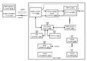
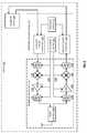
- FIG. 1is a schematic block diagram of an embodiment of a wireless power system that includes a wireless power (WP) transmit (TX) unit 10 and one or more devices 12 - 14 .
- the WP TX unit 10includes a processing module 18 , a WP transceiver 20 , and a power TX circuit 16 .
- Each device 12 - 14includes a WP receive (RX) circuit 22 , 28 , a processing module 26 , 32 , and a WP transceiver 24 , 30 .
- the device 12 - 14will most likely include a plurality of other components depending on its desired functionality.
- the device 12 - 14may be a cell phone, a personal audio/video player, a video game unit, a toy, etc. and includes the corresponding circuitry.
- the processing modules 18 , 26 , 32 of the WP TX unit 10 and in each of the devices 12 - 14may each be a single processing device or a plurality of processing devices.
- a processing devicemay be a microprocessor, micro-controller, digital signal processor, microcomputer, central processing unit, field programmable gate array, programmable logic device, state machine, logic circuitry, analog circuitry, digital circuitry, and/or any device that manipulates signals (analog and/or digital) based on hard coding of the circuitry and/or operational instructions.
- the processing module 18 , 26 , 32may have an associated memory and/or memory element, which may be a single memory device, a plurality of memory devices, and/or embedded circuitry of the processing module 18 , 26 , 32 .
- a memory devicemay be a read-only memory, random access memory, volatile memory, non-volatile memory, static memory, dynamic memory, flash memory, cache memory, and/or any device that stores digital information.
- the processing module 18 , 26 , 32includes more than one processing device, the processing devices may be centrally located (e.g., directly coupled together via a wired and/or wireless bus structure) or may be distributedly located (e.g., cloud computing via indirect coupling via a local area network and/or a wide area network).
- the processing module 18 , 26 , 32implements one or more of its functions via a state machine, analog circuitry, digital circuitry, and/or logic circuitry
- the memory and/or memory element storing the corresponding operational instructionsmay be embedded within, or external to, the circuitry comprising the state machine, analog circuitry, digital circuitry, and/or logic circuitry.
- the memory elementstores, and the processing module 18 , 26 , 32 executes, hard coded and/or operational instructions corresponding to at least some of the steps and/or functions illustrated in FIGS. 1-28 .
- the WP TX unit 10communicates with the WP transceivers 24 , 30 of the devices 12 - 14 via one or more control channels 34 that use one or more frequencies in the ISM bands 36 and/or one or more frequencies in another non-licensed frequency band(s) 38 .
- the communication via the control channel 34may use one or more standardized protocols 40 , 44 and/or one or more proprietary protocols 42 , 46 .
- the standardized protocols 40 , 44may include Bluetooth (2400 MHz), HIPERLAN (5800 MHz), IEEE 802.11 (2400 MHz and 5800MHz), and IEEE 802.15.4 (personal area networks using 915 MHz or 2400 MHz).
- the ISM bands 36include:
- Each of the WP power transceivers 20 , 24 , 30(e.g., in the WP TX unit 10 and in each of the devices 12 - 14 ) includes baseband processing (which may be done by the corresponding processing module 18 , 26 , 32 ), a radio frequency (RF) and/or a millimeter wave (MMW) transmitter section, and an RF and/or MMW receiver section.
- baseband processingwhich may be done by the corresponding processing module 18 , 26 , 32
- RFradio frequency
- MMWmillimeter wave
- the baseband processingconverts outbound data into outbound symbol stream in accordance with one or more wireless communication standards (e.g., GSM, CDMA, WCDMA, HSUPA, HSDPA, WiMAX, EDGE, GPRS, IEEE 802.11, Bluetooth, ZigBee, universal mobile telecommunications system (UMTS), long term evolution (LTE), IEEE 802.16, evolution data optimized (EV-DO), proprietary protocol, etc.).
- wireless communication standardse.g., GSM, CDMA, WCDMA, HSUPA, HSDPA, WiMAX, EDGE, GPRS, IEEE 802.11, Bluetooth, ZigBee, universal mobile telecommunications system (UMTS), long term evolution (LTE), IEEE 802.16, evolution data optimized (EV-DO), proprietary protocol, etc.
- Such a conversionincludes one or more of: scrambling, puncturing, encoding, interleaving, constellation mapping, modulation, frequency spreading, frequency hopping, beamforming, space-time-block encoding, space-frequency-block en
- the transmitter sectionconverts the outbound symbol stream into an outbound RF signal that has a carrier frequency within a given frequency band (e.g., ISM bands 36 ). In an embodiment, this may be done by mixing the outbound symbol stream with a local oscillation to produce an up-converted signal. One or more power amplifiers and/or power amplifier drivers amplifies the up-converted signal, which may be RF bandpass filtered, to produce the outbound RF signal. In another embodiment, the transmitter section includes an oscillator that produces an oscillation.
- the outbound symbol streamprovides phase information (e.g., +/ ⁇ [phase shift] and/or ⁇ (t) [phase modulation]) that adjusts the phase of the oscillation to produce a phase adjusted RF signal, which is transmitted as the outbound RF signal.
- phase informatione.g., +/ ⁇ [phase shift] and/or ⁇ (t) [phase modulation]
- the outbound symbol streamincludes amplitude information (e.g., A(t) [amplitude modulation]), which is used to adjust the amplitude of the phase adjusted RF signal to produce the outbound RF signal.
- the transmitter sectionincludes an oscillator that produces an oscillation.
- the outbound symbolprovides frequency information (e.g., +/ ⁇ f [frequency shift] and/or f(t) [frequency modulation]) that adjusts the frequency of the oscillation to produce a frequency adjusted RF signal, which is transmitted as the outbound RF signal.
- the outbound symbol streamincludes amplitude information, which is used to adjust the amplitude of the frequency adjusted RF signal to produce the outbound RF signal.
- the transmitter sectionincludes an oscillator that produces an oscillation.
- the outbound symbolprovides amplitude information (e.g., +/ ⁇ A [amplitude shift] and/or A(t) [amplitude modulation) that adjusts the amplitude of the oscillation to produce the outbound RF signal.
- the receiver sectionreceives and amplifies an inbound RF signal to produce an amplified inbound RF signal.
- the receiver sectionmay then mix in-phase (I) and quadrature (Q) components of the amplified inbound RF signal with in-phase and quadrature components of a local oscillation to produce a mixed I signal and a mixed Q signal.
- the mixed I and Q signalsare combined to produce an inbound symbol stream.
- the inbound symbolmay include phase information (e.g., +/ ⁇ [phase shift] and/or ⁇ (t) [phase modulation]) and/or frequency information (e.g., +/ ⁇ f [frequency shift] and/or f(t) [frequency modulation]).
- the inbound RF signalincludes amplitude information (e.g., +/ ⁇ A [amplitude shift] and/or A(t) [amplitude modulation]).
- the receiver sectionincludes an amplitude detector such as an envelope detector, a low pass filter, etc.
- the baseband processingconverts the inbound symbol stream into inbound data (e.g. control channel data) in accordance with one or more wireless communication standards (e.g., GSM, CDMA, WCDMA, HSUPA, HSDPA, WiMAX, EDGE, GPRS, IEEE 802.11, Bluetooth, ZigBee, universal mobile telecommunications system (UMTS), long term evolution (LTE), IEEE 802.16, evolution data optimized (EV-DO), proprietary protocol, etc.).
- wireless communication standardse.g., GSM, CDMA, WCDMA, HSUPA, HSDPA, WiMAX, EDGE, GPRS, IEEE 802.11, Bluetooth, ZigBee, universal mobile telecommunications system (UMTS), long term evolution (LTE), IEEE 802.16, evolution data optimized (EV-DO), proprietary protocol, etc.
- Such a conversionmay include one or more of: digital intermediate frequency to baseband conversion, time to frequency domain conversion, space-time-block decoding, space-frequency-block decoding, demodulation, frequency spread decoding, frequency hopping decoding, beamforming decoding, constellation demapping, deinterleaving, decoding, depuncturing, and/or descrambling.
- the WP TX unit 10communicates with the devices 12 - 14 via the control channel to facilitate efficient wireless power transfer from the WP TX unit 10 to the power RX circuit 22 , 28 of the devices 12 - 14 .
- the communicationmay be to determine which frequency to use, to reposition the device 12 - 14 to improve magnetic coupling, to tune the components of the power TX circuit 16 and/or the power RX circuit 22 , 28 , to indicate desired power levels, to adjust power levels, etc.
- the WP TX unit 10 and the devices 12 - 14communicate to provide a desired performance level of wireless energy transfer.
- the receive unit processing module 26 , 32functions to identify the control channel protocol used by the wireless power transmit unit 10 for control channel communications.
- the control channelincludes one of a plurality of control channel protocols that includes at least one or more standard control channel protocols and/or one or more proprietary control channel protocols.
- the transmit unit transceiver 20uses one of the control channel protocols and is capable of using a subset of the plurality of control channel protocols. For instance, one transmit unit transceiver 20 may use a Bluetooth protocol or a proprietary protocol for its control channel protocol, while another transmit unit transceiver 20 of another wireless power transmit unit 10 may use a different control channel protocol. As such, the receive unit needs to identify the control channel protocol.
- the receive unit processing module 26 , 32may identify the control channel protocol by interpreting a beacon signal transmitted by the transmit unit transceiver to determine the control channel protocol. Alternatively, or in addition to the preceding example, the receive unit processing module 26 , 32 may identify the control channel protocol by receiving a set-up communication from the transmit unit transceiver 20 using a default control channel protocol. As another alternative, or in addition to one or more of the preceding examples, the receive unit processing module 26 , 32 may identify the control channel protocol by scanning a frequency spectrum for control channel activity to produce scanned frequency spectrum and identify the control channel protocol from the scanned frequency spectrum. As yet another alternative, or in addition to one or more of the preceding examples, the receive unit processing module 26 , 32 may identify the control channel protocol by evoking a trial and error system using known control channel protocols.
- the receive unit processing module 26 , 32determines whether the receive unit transceiver is capable of communication using the control channel protocol. For example, the processing module is determining whether the receive unit transceiver 24 , 30 be configured to support the control channel protocol. When the receive unit transceiver 24 , 30 is capable of communication using the control channel protocol, the processing module coordinates configuration of the receive unit transceiver to transceive the communication regarding the wireless power magnetic field via the control channel. Configuring of the receive unit transceiver 24 , 30 is discussed in greater detail with reference to FIG. 6 .
- the transmit unit transceiver 20 and the receive unit transceiver 24 , 30may negotiate which control channel protocol to use.
- the transmit unit transceivermay transceive negotiation information (e.g., what protocols they each support, desired data rate, available bandwidth, etc.) with the receive unit transceiver to mutually select the control channel protocol.
- the processing module 26 , 32determines whether the receive unit transceiver is lacking hardware or lacking software to support the control channel protocol. When the receive unit transceiver is lacking software, the processing module generates a network message to download the software to support the control channel protocol. Once the software is downloaded, the receive unit transceiver 24 , 30 is configured to support the control channel protocol.
- the wireless power transmit circuit 16With the control channel established between the wireless power transmit unit 10 and the device 12 , 14 , the wireless power transmit circuit 16 generates a wireless power magnetic field in accordance with the control channel data (e.g., power level, frequency, tuning, etc.).
- the wireless power receive circuit 22 , 28converts the wireless power magnetic field into a voltage, which may be used to charge a battery of the device and/or to power at least a portion of the device 12 , 14 .
- FIG. 2is a schematic block diagram of another embodiment of a wireless power system that includes a wireless power (WP) transmit (TX) unit 10 and one or more devices.
- the WP TX unit 10includes a processing module 18 , a WP transceiver 20 , an RFID (radio frequency identification) tag and/or reader 48 , and a power TX circuit 16 .
- Each device 12 - 14includes a WP receive (RX) circuit 24 , 28 , a processing module 26 , 32 , an RFID tag and/or reader 50 , 52 , and a WP transceiver 24 , 30 .
- the device 12 - 14will most likely include a plurality of other components depending on its desired functionality.
- the devicemay be a cell phone, a personal audio/video player, a video game unit, a toy, etc. and it includes the corresponding circuitry.
- the RFID tags 48 , 50 , 52include information regarding the wireless power requirements and capabilities of the devices 12 - 14 and of the WP TX unit 10 .
- the informationmay include the communication protocol to use (e.g., one or more of the standardized protocols 40 , 44 or one or more of the proprietary protocols 42 , 46 ), the wireless power frequency spectrum, impedance matching information, battery charging requirements, etc.
- the RFID readers and tags 48 , 50 , 52may be active or passive devices and may use backscattering to communicate.
- the devices 12 - 14initially communicate with the WP TX unit 10 to exchange set up information and, once set up, the devices 12 - 14 communicate with the WP TX unit 10 via the WP transceivers 20 , 24 , 30 .
- FIG. 3is a schematic block diagram of another embodiment of a wireless power system that includes a wireless power (WP) transmit (TX) unit 10 and one or more devices 12 - 14 .
- the WP TX unit 10includes a processing module 18 , an RFID (radio frequency identification) tag and/or reader 48 , and a power TX circuit 16 .
- Each device 12 - 14includes a WP receive (RX) circuit 22 , 28 , a processing module 26 , 32 , and an RFID tag and/or reader 50 , 52 .
- the device 12 - 14will most likely include a plurality of other components depending on its desired functionality.
- the devicemay be a cell phone, a personal audio/video player, a video game unit, a toy, etc. and it includes the corresponding circuitry.
- the RFID tags 48 , 50 , 52include information regarding the wireless power requirements and capabilities of the devices 12 - 14 and of the WP TX unit 10 .
- the informationmay include the communication protocol to use (e.g., one or more of the standardized protocols 54 or one or more of the proprietary protocols 56 ), the wireless power frequency spectrum, impedance matching information, battery charging requirements, etc.
- the WP TX unit 10 and the devices 12 - 14use the RFID tags and readers 48 , 50 , 52 as the primary communication means between them.
- the RFID readers and tags 48 , 50 , 52may be active or passive devices and may use backscattering to communicate.
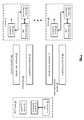
- FIG. 4is a schematic block diagram of another embodiment of a wireless power system that includes the WP TX unit 10 and a device 58 .
- the device 58includes the power receiver circuit 62 , a battery charger 64 , a battery 66 , a DC-to-DC converter 68 , the processing module 70 , memory 72 , a plurality of input/output (I/O) modules 74 , a plurality of circuit modules 76 - 78 , a clock generation unit 80 , and a power management unit 82 .
- the device 58may be one of the devices 12 - 14 of FIGS. 1-3 .
- the WP TX unit 10After the WP TX unit 10 and the device 58 have established communication, the WP TX unit 10 generates a magnetic field that is received by the power receiver circuit 62 , which is integrated into device 58 .
- the power receiver circuit 62generates an AC voltage from the magnetic field, rectifies the AC voltage to produce a rectified voltage, and filters to the rectified voltage to produce a DC voltage rail (e.g., V+ and V ⁇ ).
- the power receiver circuit 62may be tuned based on control signals provided by the processing module 70 .
- the tuningincludes adjusting one or more electromagnetic properties, such as the quality factor of the circuit, adjusting impedance, current limiting, etc., of the magnetic field and/or the wireless power receiver circuit 62 .
- the battery charger 64converts the DC voltage rail into a battery charge voltage, which it provides to the battery 66 .
- the battery charger 64monitors the charging to insure proper charging in accordance with the type of battery and, once the battery 66 is charged, may implement a trickle charge.
- the processing module 70may provide control signals to the battery charger 64 to regulate the charging in accordance with the type of battery.
- the DC-to-DC converter 68converts the battery voltage (e.g., 1.5 volts, 4.2 volts, etc.) into one or more supply voltages (e.g., 1 volt, 2.2 volts, 3.3 volts, 5 volts, 12 volts, etc.).
- the DC-to-DC converter 68provides the supply voltages to one or more of the other modules 70 , 72 , 74 , 76 , 78 , 80 under the direction of the power management module 82 .
- the power management module 82functions to control power consumption by the device 58 to an optimal level (e.g., balancing of performance and battery life).
- the power management module 82may treat each module 70 , 72 , 74 , 76 , 78 , 80 as a separate power island that can be individually controlled. For example, when a circuit module 76 - 78 is inactive, the power management module 82 may remove power from the circuit module 76 - 78 . As another example, the power management module 82 may reduce the voltage provided to a circuit module 76 - 78 when the circuit module 76 - 78 does not need to operate at its maximum potential.
- the power management module 82may control the clock signals provided to each circuit module 76 - 78 that uses a clock signal. For example, when a circuit is idle, the power management module 82 may provide a reduced supply voltage to the circuit module 76 - 78 , but disable the clock signal provided to the circuit module 76 - 78 . In this way, minimal power is consumed, but the circuit module 76 - 78 may be quickly activated when it is needed. As another example, the power management module 82 may reduce the frequency of a clock signal for a circuit module 76 - 78 when the circuit module 76 - 78 does not need to operate at its maximum potential.
- the plurality of circuit modules 76 - 78provides at least some of the functionality for the device 58 .
- the circuit modules 76 - 78may provide a digital image capture function, a digital image display function, an audio file playback function, a data messaging function, a voice call function, etc.
- the plurality of input/output (I/O) modules 74provides the interface to the user input/output components (e.g., speaker, microphone, display, buttons, etc.) of the device 58 .
- a circuit modulemay generate outbound data (e.g., a captured digital image).
- the processing moduleprocesses the outbound data to produce processed data (e.g., generates a digital image file) and provides the processed outbound data to an input/output module for display on a peripheral output component (e.g., an LCD display).
- a peripheral output componente.g., an LCD display
- an input/output modulemay receive inbound data (e.g., a place call command) from a peripheral input component (e.g., keypad of the device) and provide it to the processing module.
- the processing moduleprocesses the inbound data to produce processed inbound data (e.g., retrieve the phone number of the target identified in the call command).
- the processing moduleprovides the processed inbound data to a circuit module, which performs a function on the processed inbound data (e.g., places the call to the target).
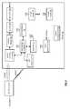
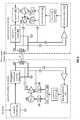
- FIG. 5is a schematic block diagram of an embodiment of a portion of a wireless power system that includes the power transmitter circuit 84 and the power receiver circuit 86 .
- the power transmitter circuit 84includes a coil (i.e., an inductor), a rectify and regulate circuit 88 , an impedance matching and excitation circuit 90 , a processing module 92 , and an RF and/or MMW transceiver 94 .
- the power receiver circuit 86includes a coil, an impedance matching and rectify circuit 96 , a regulate circuit 98 , and an RF and/or MMW transceiver 100 .
- the power receiver circuit 86is coupled to the battery charger 104 and the processing module 102 .
- the power receiver circuit 84is readily integrated into the device and uses components of the device (e.g., the processing module 102 ).
- the power receiver circuit 86is not a standalone component coupled to the device, but an integral part of the device.
- the device 12 , 14 , 58will typically include a housing, which houses the power receiver circuit 86 , the battery charger 104 , the battery 106 , and the RF/MMW transceiver 100 , the processing module 102 , and the components as shown in FIG. 4 .
- the rectify and regulate circuit of the power transceiver circuit 84converts an AC voltage (e.g., 110 VAC, 220 VAC, etc.) into a DC voltage (e.g., 160 VDC, 320 VDC, etc.).
- the impedance matching and excitation circuit 90couple the TX power coil to the DC voltage in an alternating pattern (e.g., a full bridge inverter, a half bridge inverter) at a given frequency (e.g., 10 MHz, etc.).
- the impedance matchingallows the LC circuit of the capacitor and coil to be tuned to a desired resonant frequency and to have a desired quality factor. For example, the LC circuit may be tuned to resonant at the excitation rate.
- the coil of the power RX 86 unitis proximal to the coil of the TX unit 84 to receive the magnetic field created by the TX coil and to create an AC voltage therefrom.
- the LC circuit of the RX coil and capacitormay be tuned to have a desired resonance and/or a desired quality factor.
- the impedance matching and rectify circuit 96rectifies the AC voltage of the RX coil to produce a DC rail voltage that is regulated via the regulation circuit.
- FIG. 6is a schematic block diagram of an embodiment of a wirelessly powered device 108 that includes the power RX circuit 110 , an RF and/or MMW data processing module 112 (which may be implemented within the processing module) and the RF and/or MMW transceiver 114 .
- the RF and/or MMW data processing module 112includes an outbound symbol conversion module 116 , a baseband control module 118 , a transceiver control module 120 , and an inbound symbol conversion module 122 .
- the RF and/or MMW transceiver 114includes a transmitter 124 and a receiver 126 .
- the transmitter 124includes a low IF (e.g., 0 to a few MHz) bandpass filter 128 , a mixing module 130 , a power amplifier (PA) 132 , and an RF bandpass filter 134 .
- the receiver 126includes an RF bandpass filter 136 , a low noise amplifier (LNA) 138 , a mixing module 140 , and a low IF bandpass filter 142 . If the transmitter 124 and receiver 126 share an antenna, the transceiver 114 further includes a TX/RX isolation circuit 144 (e.g., a circulator, a transformer balun, a TX/RX switch, etc.).
- a TX/RX isolation circuit 144e.g., a circulator, a transformer balun, a TX/RX switch, etc.
- the data processing module 112configures itself based on the communication protocol being implemented and the corresponding data modulation.
- the transceiver control moduleprovides control signals to the transceiver 114 to adjust one or more of the components thereof based on the protocol being implemented.
- the data processing module 112 and the transceiver 114may be configured to implement one or more of the standard communication protocols and/or one or more of the proprietary communication protocols.
- the device 108may include one or more configurable RF/MMW data processing modules 112 and/or one or more configurable RF/MMW transceivers 114 .
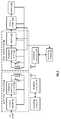
- FIG. 7is a schematic block diagram of an embodiment of a portion of a wireless power system that includes the power transmitter circuit 144 and the power receiver circuit 146 .
- the power transmitter circuit 144includes a rectify and regulate circuit 148 , an impedance matching and excitation circuit 150 , a processing module 152 , an NFC modulator/demodulator 154 , and an NFC coil 156 .
- the power receiver circuit 146includes an impedance matching and rectify circuit 158 , a regulate circuit 160 , an NFC modulator/demodulator 162 , and an NFC coil 164 .
- the power receiver circuit 146is coupled to the battery charger (not shown in figure) and the processing module 166 .
- the rectify and regulate circuit 148 of the power transmitter circuit 144converts an AC voltage (e.g., 110 VAC, 220 VAC, etc.) into a DC voltage (e.g., 160 VDC, 320 VDC, etc.).
- the impedance matching and excitation circuit 150couple the TX power coil to the DC voltage in an alternating pattern (e.g., a full bridge inverter, a half bridge inverter) at a given frequency (e.g., 10 MHz, etc.).
- the impedance matchingallows the LC circuit of the capacitor and coil to be tuned to a desired resonant frequency and to have a desired quality factor. For example, the LC circuit may be tuned to resonant at the excitation rate.
- the coil of the power receiver circuit 146is proximal to the coil of the transmitter circuit 144 to receive the magnetic field created by the TX coil and to create an AC voltage therefrom.
- the LC circuit of the RX coil and capacitormay be tuned to have a desired resonance and/or a desired quality factor.
- the impedance matching and rectify circuit 158rectifies the AC voltage of the RX coil to produce a DC rail voltage that is regulated via the regulation circuit 160 .
- the devicecommunicates to the power transmitter circuit 144 via NFC (near field communication) 170 .
- NFCnear field communication
- the processing module 166when the device has data to convey to the power transmitter circuit 144 , the processing module 166 generates the data, which it provides to the NFC modulator/demodulator 162 .
- the NFC mod/demodulator 162modulates the data at a given frequency (e.g., 13 MHz, 900 MHz, etc.) that drives the NFC coil 164 .
- the NFC coil 164creates a magnetic field that is received by the NFC coil 156 of the power transmitter circuit 144 .
- the NFC mod/demod unit 154demodulates the signal produced by the NFC coil 156 to recover the transmitted data, which is provided to the processing module 152 .
- Data from the power transmitter circuit 144 to the deviceis processed in a similar manner.
- FIG. 8is a schematic block diagram of another embodiment of a portion of a wireless power system that includes the power transmitter circuit 172 and the power receiver circuit 174 .
- the power transmitter circuit 172includes a rectify and regulate circuit 176 , an impedance matching and excitation circuit 178 , a processing module 190 , an NFC modulator/demodulator 188 , 200 , and a share WP & NFC coil 202 .
- the power receiver circuit 174includes an impedance matching and rectify circuit 204 , a regulate circuit 206 , an NFC modulator/demodulator 216 , 220 , and an NFC coil 222 .
- the power receiver circuit 174is coupled to the battery charger (not shown in figure) and the processing module 218 .
- the rectify and regulate circuit 176 of the power transmitter circuit 172converts an AC voltage (e.g., 110 VAC, 220 VAC, etc.) into a DC voltage (e.g., 160 VDC, 320 VDC, etc.).
- the impedance matching and excitation circuit 178couple the TX power coil 202 to the DC voltage in an alternating pattern (e.g., a full bridge inverter, a half bridge inverter) at a given frequency (e.g., 10 MHz, etc.).
- the impedance matchingallows the LC circuit of the capacitor and coil to be tuned to a desired resonant frequency and to have a desired quality factor. For example, the LC circuit may be tuned to resonant at the excitation rate.
- the coil 202 of the power receiver circuit 174is proximal to the coil 222 of the power transmitter circuit 172 to receive the magnetic field created by the TX coil 202 and to create an AC voltage therefrom.
- the LC circuit of the RX coil 222 and capacitormay be tuned to have a desired resonance and/or a desired quality factor.
- the impedance matching and rectify circuit 204rectifies the AC voltage of the RX coil 222 to produce a DC rail voltage that is regulated via the regulation circuit.
- the devicecommunicates with the WP TX unit via NFC (near field communication) using the shared WP & NFC coils 202 , 222 .
- NFCnear field communication
- the processing module 218when the device has data to convey to the WP TX unit, the processing module 218 generates the data, which it provides the NFC data modulator 216 .
- the NFC modulator 216modulates the data at a given frequency (e.g., 13 MHz, 900 MHz, etc.) to produce an amplitude component (A(t)) 212 and a phase component ( ⁇ (t)) 214 .
- the phase component 214adjusts the phase of an oscillation (cos ⁇ (t)) to produce a phase adjusted oscillation (cos( ⁇ (t)+ ⁇ (t))) 210 .
- the power amplifier 208amplifies the phase adjusted oscillation 210 by the amplitude component 212 to produce an amplitude modulated and phase adjusted signal (A(t)cos( ⁇ (t)+ ⁇ (t))).
- the signalis AC coupled to the shared WP & NFC coil 222 for conveyance to the WP TX unit.
- the shared coil 202 of the WP TX unitreceives the signal (e.g., A 0 cos( ⁇ 0 (t))*A(t)cos( ⁇ (t)+ ⁇ (t)), where A 0 is the amplitude of the WP signal and ⁇ 0 corresponds to the frequency of the WP signal).
- the NFC signal componentis AC coupled to the data demodulator 200 and the WP component is provided to the impedance matching circuit 178 .
- the data demodulator 200recovers the data from the amplitude component 186 and the phase component 184 and provides the data to the processing module 190 .
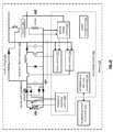
- FIG. 9is a schematic block diagram of another embodiment of a wireless power system that includes the WP TX unit 226 and a device 228 .
- the device 228includes the WP coil 230 , the power RX circuit 232 , the battery charger 234 , the battery 236 , a multiplexer 238 or the like, the DC-to-DC converter 240 , the processing module 242 , the IO interface modules 244 , the memory 246 , the power management unit 248 , an NFC power recovery module 252 , and/or an RF/MMW power recovery module 250 .
- the NFC power recovery module 252 and/or RF/MMW power recovery module 250when the battery 236 is dead or near dead and as insufficient power to power minimal circuitry to facilitate battery charging, the NFC power recovery module 252 and/or RF/MMW power recovery module 250 generate an emergency voltage to provide the energy to initiate battery charging.
- the emergency supply generatorsmay be disabled and the supply voltage V 1 may be used to power the device 228 during charging and/or after charging is complete (i.e., in a trickle charge mode). Note that as long as WP energy is being received, the device 228 may be powered by V 1 or another voltage derived from the WP energy.
- FIG. 10is a schematic block diagram of another embodiment of a wirelessly powered device 254 that includes the processing module 256 , the rectify and impedance matching circuit (e.g., capacitors and diodes) 258 , the RX coil 260 , a buck &/or boost converter 262 , a trickle charge circuit 264 , a battery 266 , and a battery current sensor 268 .
- the processing module 256implements a battery charger controller 270 , a boost controller 272 , a buck controller 274 , an impedance matching control 280 , and an RF/MMW and/or NFC data processing module 276 .
- the processing module 256may further implement the power management unit 282 .
- processing module 256may be fabricated on a single integrated circuit or on a multiple integrated circuit with one or more of the components of the converter 262 , the rectifier circuit 258 , the trickle charge circuit 264 , and/or the battery current sense 268 .
- the RX coil 260(which may include one or more adjustable inductors) receives a magnetic field from the WP TX unit and creates an AC voltage therefrom.
- the adjustable capacitoris tuned (alone in conjunction with the RX coil 260 ) to a desired resonance, impedance, and/or quality factor to facilitate the creation of the AC voltage.
- the full bridge rectifiere.g., the diodes
- rectify the AC voltageto produce a rectified voltage that is filtered by the capacitor to produce a DC rail voltage (e.g., 3-20 volts).
- the buck and/or boost converter 262is enabled in a buck converter mode when the DC voltage rail is to be stepped down to produce battery charge voltage (and the supply voltage Vdd for the device) and is enabled in boost converter mode when the DC rail voltage is to be stepped up to produce the battery charge voltage (and the supply voltage Vdd). Note that when the buck and/or boost converter 262 is in the boost mode, the buck transistor is enabled. Further note that the buck and/or boost converter 262 may include multiple inductors, transistors, diodes, and capacitors to produce multiple supply voltages.
- the battery charge control module 270monitors the battery current and voltage to insure charging is in accordance with the charging requirements of the battery 266 .
- the battery 266is disconnected from the converter 262 (which may be disabled or enabled to provide Vdd) and the battery 266 may be trickle charged. Note that when the WP is lost, the battery 266 is coupled to provide the power for the device 254 .
- FIG. 11is an example state diagram of a processing module of a wirelessly powered device 12 - 14 , 58 that includes six states 286 : idle 284 , charge set up 288 , charge 290 , trickle charge 292 , WP operated—power management 294 , and battery operated—power management 296 .
- the devicestarts in the idle state 284 and waits to detect the WP TX unit, WP operation enablement, or battery operation enablement.
- the devicemay be in one of the charge states 286 and the WP operated—power management state 294 concurrently.
- the deviceWhen the device detects the WP TX unit (e.g., via RFID communication, via control channel communication, via sensing a magnetic field, etc.), the device transitions from the idle state 284 to the charge set up state 288 . When in the charge set up state 288 , the device functions as referenced in FIGS. 12 and/or 13 , which will be subsequently discussed. The device transitions back to the idle state 284 if the set up failed, which may result from failing to establish a control channel communication, the WP TX unit not being able to currently service the device, circuit damage, a bad battery, or loss of connection.
- the WP TX unite.g., via RFID communication, via control channel communication, via sensing a magnetic field, etc.
- the devicetransitions to the charge state 290 when the charge set up is complete. While in the charge state 290 , the device functions as referenced in FIGS. 14 and/or 15 , which will be subsequently discussed.
- the devicetransitions to the idle state 284 if the charging failed or the charging is complete and the battery does not require a trickle charge. If the charging is complete and the battery will be trickled charge, the device transitions to the trickle charge state 292 . The device stays in this state until a failure occurs (e.g., loss of connection with the WP TX unit) or until the trickle charge is complete. In either event, the device transitions back to the idle state 284 .
- the devicetransitions to the WP operated—power manage state 294 when the device is enabled and is connected to the WP TX unit. While in this state, the device functions as referenced in FIG. 16 , which will be subsequently discussed.
- the devicetransitions back to the idle state 284 when the device is disabled (e.g., turned off, placed in a sleep mode, etc.). Note that while the device is in this state, it may also be in one of the charge states.
- the devicetransitions from the WP operated state 294 to the battery operated—power manage state 296 when the device is disconnected from the WP TX unit.
- the devicemay also enter the battery-operated state 296 from the idle state 284 when the device is enabled and not connected to the WP TX unit. While in this state, the device functions as referenced in FIG. 17 , which will be subsequently discussed.
- the devicetransitions back to the WP operated state 294 when the device is again connected to the WP TX unit.
- the devicetransitions back to the idle state 284 when the device is disabled (e.g., turned off, sleep mode, low battery, etc.).
- the devicemay include an integrated circuit (IC) that includes at least a portion of a wireless power receiver circuit 86 (e.g., an on-chip coil, an on-chip variable capacitor, components of the impedance matching & rectify circuit 96 (diodes of the rectify circuit may be off-chip), and components of the regulation circuit 98 ), a transceiver, and a processing module.
- a wireless power receiver circuite.g., an on-chip coil, an on-chip variable capacitor, components of the impedance matching & rectify circuit 96 (diodes of the rectify circuit may be off-chip), and components of the regulation circuit 98 ), a transceiver, and a processing module.
- the wireless power receiver circuitconverts the electromagnetic signal into a voltage and the transceiver, when operable, transceives a control channel communication.
- the processing moduleis operable to transition the device from an idle state to a charge state when a wireless power transmitter unit is detected.
- the processing moduleis further operable to transition the device from the idle state to a wireless power operated state when a wireless power transmit circuit is detected and the device is enabled.
- the processing moduleis still further operable to transition the device from the idle state to a battery operated state when the device is enabled and the wireless power transmit circuit is not detected.
- the processing modulemay be operable to detect availability of the wireless power transmitter unit via the control channel communication. The processing module may then, when the wireless power transmitter unit is available, determine battery charging needs and whether the device is active. The processing module may then, when the battery charging needs compares unfavorable to a threshold, initiate battery charging using the voltage. The processing may, when the device is active, enable wireless power operation and, when the wireless power transmitter is not available, enable battery operated mode for the device.
- FIG. 12is a logic diagram of an embodiment of a method for a charge set up state 298 that begins with the device working with the WP TX unit to select a standardized communication protocol 300 .
- Examples of the communication protocolswere presented with reference to FIGS. 1-3 . Note this step may begin by assuming a default communication protocol (e.g., RFID, Bluetooth, etc.) to initiate communication and then, once communication is established, selecting another communication protocol.
- the methodcontinues with the device determining whether the device is synchronized via a control channel with the WP TX unit 302 . In other words, is a usable control channel established between the device and the WP TX unit? If yes, the method continues with the device establishing a control channel communication with the WP TX unit 304 and exiting the state 306 .
- a default communication protocole.g., RFID, Bluetooth, etc.
- the methodcontinues with the device determining whether it has exhausted its standardized communication protocols 308 (e.g., the ones it is capable of executing). If not, the process repeats with the device selecting another standardized protocol 300 . If the standardized protocols are exhausted, the method continues with the device selecting a proprietary communication protocol 310 . Note that the method may begin with proprietary protocols and if they are exhausted, then try standardized protocols. Further note that there may be no distinction between a standard protocol and a proprietary protocol such that the method attempts to find a usable protocol regardless of whether it is a standard or proprietary protocol.
- the methodcontinues with the device determining whether the device is synchronized via a control channel with the WP TX unit using the proprietary protocol 312 . If yes, the method continues with the device establishing a control channel communication with the WP TX unit 314 using the proprietary protocol and exiting the state 318 .
- the methodcontinues with the device determining whether it has exhausted its proprietary communication protocols 316 (e.g., the ones it is capable of executing). If not, the process repeats with the device selecting another proprietary protocol 310 . If the proprietary protocols are exhausted, the method continues with the device exiting this state due to a failure 318 .
- proprietary communication protocols 316e.g., the ones it is capable of executing.
- FIG. 13is a logic diagram of another embodiment of a method for a charge set up state 320 that begins with the device reading an RFID tag of the WP TX unit 322 to determine a desired control channel protocol. The method continues with the device determining whether it is capable of executing the desired control channel protocol 324 . If yes, the method continues with the device establishing a control channel communication with the WP TX unit 326 and exiting the state 328 .
- the methodcontinues with the device determining whether it includes the hardware to support the desired control channel protocol 330 . For example, does it include the NFC circuitry, the RF circuitry, and/or the MMW circuitry to support the operating frequency, power requirements, transmission range, etc. of the desired control channel protocol. If yes, then the device is lacking the desired control channel protocol software and the method continues with the device downloading the software for the desired control channel protocol 332 . After the device has the software, the method continues with the device establishing a control channel communication with the WP TX unit 326 .
- the methodcontinues with the device determining whether it can use RFID as the control channel protocol with the WP TX unit 334 .
- the devicerequests that they use RFID, if the WP TX unit agrees, then the method continues with the device using RFID for the control channel with the WP TX unit 336 . If the device cannot use RFID for the control channel, then the device exits the state due to a failure 338 .
- FIG. 14is a logic diagram of an embodiment of a method for a charge state 340 that begins with the device determining the level of its battery 342 (e.g., the battery life left based on the battery type, the power demands of the device, etc.). The method continues with the device determining if the battery needs charging 344 - 346 . For example, has the power capacity of the battery been drained below a threshold, which may be based on battery life, not being fully charged, and/or some other criteria.
- a thresholdwhich may be based on battery life, not being fully charged, and/or some other criteria.
- the methodbranches back to the beginning if the battery does not need charging and branches to the next step if it does.
- the devicecommunicates with the WP TX unit to determine one or more of: impedance matching settings, operating frequency, power level, number of coils, etc 348 .
- the methodcontinues with the device determining whether it needs to adjust one or more of the impedance of its power RX circuit, the operating frequency of the power RX circuit, the power level, etc. and making the appropriate adjustments as needed 350 .
- the methodcontinues with the device setting charging parameters 352 (e.g., Vdd, current limits, trickle level, charge time intervals, etc.).
- the methodcontinues with the device charging the battery and monitoring the charging 354 (e.g., the charging current and/or the charging voltage).
- the devicealso determines whether it is still in range of the WP TX unit 356 . If so, the method continues with the device determining whether the charging is complete 358 . If not, the process continues by setting (i.e., adjusting if needed in subsequent repetitions of the loop) the charging parameters 348 . If the device is out of range, the method continues with the device exiting this state due to a failure 360 . The device also exits this state 360 if the battery is charged.
- charging parameters 352e.g., Vdd, current limits, trickle level, charge time intervals, etc.
- the methodcontinues with the device charging the battery and monitoring the charging 354 (e.g., the charging current and/or the charging voltage).
- FIG. 15is a diagram of an example of a graph of charge need versus charge efficiency that may be used by the device to determine whether charging is needed as mentioned in the logic diagram of FIG. 14 .
- the determination of whether charging is neededis a sliding scale that varies based on battery life and charging efficiency. As such, when the battery life is high, don't charge the battery unless it can be done efficiently. As the battery life diminishes, the need to charge it is greater, which, at some point, outweighs the desired for the charging to be done efficiently.
- FIG. 16is a logic diagram of an embodiment of a method for a wirelessly powered power management state 362 that begins with the device determining whether the battery needs charging 364 . If not, the method continues with the device disconnecting the battery from the charger 366 . The device may engage a trickle charge if desired or required per the battery charging requirements. The method continues with the device determining the activation status of the circuit modules 368 (e.g., disabled, active, idle, etc.). The method continues with the device determining clock signals for the active circuit modules 370 (e.g., select clock rate to just meet operational needs, which will typically be less than a maximum clock rate).
- the active circuit modules 370e.g., select clock rate to just meet operational needs, which will typically be less than a maximum clock rate.
- the methodcontinues with the device determining supply voltages for the active and idle circuit modules 372 .
- the devicemay set the power levels for idle circuit modules at a level to provide just enough energy to determine whether the circuit module is to remain in the idle state or transition into an active state.
- the devicemay set the power level for active circuits modules to a level just sufficient enough for the circuit module to perform its task, which will typically be less than a maximum power level.
- the methodcontinues with the device enabling the clock signals for the active circuits and providing the selected power levels to the active and idle circuit modules 374 .
- the methodcontinues with the device determining whether it is still connected to the WP TX unit 376 . If yes, the method repeats from the beginning. If not, the method continues with the device exiting the state 378 . Note that in this state, power management of the device is a less critical task than when the device is battery operated. As such, the setting of the clock signal rates and power levels may be set near maximum values to enhance performance.
- FIG. 17is a logic diagram of an embodiment of a method for a battery powered power management state 380 that begins with the device disconnecting the battery from the charger and connecting it as the primary power source 382 . The method continues with the device determining activation status of the circuit modules 384 (e.g., disabled, active, idle, etc.). The method continues with the device determining, for each active circuit module, a minimum acceptable clock signal and a minimum acceptable supply voltage 386 (e.g., Vdd).
- a minimum acceptable clock signale.g., Vdd
- the methodcontinues with the device enabling generation of the minimum acceptable clock signals by the clock generator and the minimum acceptable supply voltages by the converter 388 .
- the methodcontinues with the device determining, for each idle circuit module, a minimum acceptable idle supply voltage and no clock signal 390 .
- the methodcontinues with the device enabling generation of the idle supply voltage by the converter 392 .
- the methodcontinues with the device determining whether it is still in the battery mode 394 . If yes, the method repeats. If not, the device exits this state 396 .
- FIG. 18is a schematic block diagram of an embodiment of a wireless power computer system that includes a computer 600 , a wireless keyboard 602 , a wireless mouse 604 , a cell phone 606 , a personal audio/video (A/V) player 608 , an external hard drive 610 , and potentially other peripheral computer devices (e.g., joy stick, touch pad, track ball, speakers, etc.).
- the computer 600may be a laptop, a panel display computer (e.g., a tablet), a conventional computer, etc. and includes a wireless power module.
- the computer 600is powered wirelessly via the power transmitter circuit 612 (i.e., a WP TX unit) and provides wireless power to the peripheral components (e.g., keyboard 602 , mouse 604 , cell phone 606 , personal AV player 608 , hard drive 610 , etc.).
- the peripheral devices 602 - 610may be wirelessly powered concurrently from the computer 600 and/or sequentially.
- Each of the peripheral devices 602 - 610wirelessly communicates with the computer 600 using conventional wireless communication protocols (e.g., Bluetooth) and/or uses the WP control channel.
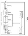
- a wireless power systemmay include a primary device (e.g., computer, television, monitor, cable set-top box, satellite set-top box, home electronic appliance, etc.) and at least one peripheral device (e.g., the peripheral devices of FIG. 35 , audio and/or video entertainment components, remote controllers, etc.).
- the primary deviceincludes a power conversion unit, a functional module, and a transceiver.
- the peripheral deviceincludes a wireless power receiver, a peripheral unit, and a transceiver.
- the power conversion unitconverts a power source into an electromagnetic signal.
- the power conversion unitmay include a power supply and a wireless power transmitter circuit.
- the power supplyconverts the power source (e.g., an AC voltage) into an output DC voltage.
- the wireless power transmitter circuitconverts the output DC voltage into the electromagnetic signal.
- the power conversion unitincludes a wireless power receiver circuit and a power conversion transmit circuit.
- the wireless power receiver circuitconverts the power source (e.g., an input electromagnetic signal) into a supply voltage.
- the power conversion transmit circuitconverts the supply voltage into the electromagnetic signal.
- the input electromagnetic signalmay have a first frequency and the electromagnetic signal may have a second frequency to minimize interference therebetween.
- the functional module of the primary deviceexecutes a function regarding peripheral information (e.g., communication protocol for the conveyance of the peripheral information, input data from the peripheral device, an input command from the peripheral device, output data for the peripheral device, and/or an output command for the peripheral device).
- peripheral informatione.g., communication protocol for the conveyance of the peripheral information, input data from the peripheral device, an input command from the peripheral device, output data for the peripheral device, and/or an output command for the peripheral device.
- peripheral informatione.g., communication protocol for the conveyance of the peripheral information, input data from the peripheral device, an input command from the peripheral device, output data for the peripheral device, and/or an output command for the peripheral device.
- peripheral informatione.g., communication protocol for the conveyance of the peripheral information, input data from the peripheral device, an input command from the peripheral device, output data for the peripheral device, and/or an output command for the peripheral device.
- the functional moduleis a central processing unit and the peripheral device is a user input device (e.g.,
- the transceiver of the primary devicecommunicates information regarding the electromagnetic signal with the transceiver of the peripheral device.
- the information regarding the electromagnetic signalincludes control channel protocol, frequency of the electromagnetic signal, impedance matching parameters, resonant frequency tuning parameters, and/or other electromagnetic properties discussed herein.
- the transceiver of the primary devicealso communicates the peripheral information with the transceiver of the peripheral device.
- the transceiversare used for wireless power control channel communication and for peripheral device functional (e.g., data and/or commands) communication.
- the primary devicemay further include a battery, a battery charger, and a processing module.
- the battery chargerutilizes the supply voltage to charge the primary battery as discussed with reference to one or more of the figures.
- the processing modulecoordinates the charging of the battery, the communicating the information regarding the electromagnetic signal, and the communicating the peripheral information.
- the wireless power receiver circuit of the peripheral deviceconverts the electromagnetic signal into a voltage as discussed with reference to one or more of the figures.
- the peripheral unit of the peripheral deviceprocesses the peripheral information. For example, the peripheral unit may generate input data for the primary device, wherein the peripheral information includes the input data. As another example, the peripheral unit may generate an input command for the primary device, wherein the peripheral information includes the input command. As another example, the peripheral unit may perform a function on output data from the primary device, wherein the peripheral information includes the output data. As another example, the peripheral unit may perform a function in accordance with an output command from the primary device, wherein the peripheral information includes the output command.
- the peripheral devicemay further include a battery, a battery charger, and a processing module.
- the battery chargerutilizes the supply voltage to charge the peripheral battery.
- the processing modulecoordinates the charging of the battery, the communicating the information regarding the electromagnetic signal, and the communicating the peripheral information.
- the primary device and/or the peripheral devicemay include an integrated circuit (IC) to support the above-described functions.
- an ICmay include at least a portion of the wireless power receiver circuit (e.g., one or more of the coil, capacitor, and diodes of the rectifying circuit may be off-chip), at least a portion of the battery charger (e.g., one or more of the switching transistors, the output filter capacitor, the inductor may be off-chip), the transceiver, and the processing module.
- FIG. 19is a schematic block diagram of an embodiment of power modules (e.g., computer power module 616 and peripheral device power module 614 ) within a wireless power computer system.
- the computer power module 616includes a wireless transceiver 620 , a power receiver circuit 622 , a battery charger 624 , a battery 626 , a power conversion transmit (TX) circuit 628 , a processing module 630 , and memory 632 .
- the peripheral device power module 614includes a wireless transceiver 634 a power receive circuit (RX ckt) 636 , a battery charger 638 , and a battery 640 .
- RX cktpower receive circuit
- the power transmit circuit 618generates a magnetic field that is received by the power receiver circuit 622 of the computer power module 616 to facilitate a wireless power transference.
- the power receiver circuit 622generates a DC rail voltage in accordance with control signals provided by the processing module 630 .
- the battery charger 624converts the DC rail voltage into a battery charge voltage, which is supplied to the battery 626 .
- the power conversion TX circuit 628generates a magnetic field that is magnetically coupled to the power RX circuit 636 of the peripheral device power module 614 .
- the power conversion TX circuit 628may be sourced by the DC rail voltage when the computer power module 616 is proximal to the power transmitter circuit 618 or the battery 626 when the computer power module 616 is not proximal to the power transmitter circuit 618 .
- the power RX circuit of the peripheral device power module 636generates a DC rail voltage from the magnetic field of the power conversion TX circuit 628 .
- the battery charger 624converts the DC rail voltage into a battery charger voltage, which is provided to the battery 626 .
- the computer power module 616communicates with the peripheral device power module 614 via the wireless transceivers 620 , 634 (e.g., RF, MMW, and/or NFC) regarding wireless power matters (e.g., frequency selection, operating frequency, impedance matching settings, power levels, etc.).
- the wireless transceivers 620 , 634may be used to convey data between the peripheral device and the computer.
- the peripheral deviceis the wireless keyboard
- the keyboard signalingmay be conveyed to the computer via the wireless transceivers.
- the wireless transceiversmay be conveyed to the computer via the wireless transceivers. Note that with multiple peripheral devices, each including a wireless transceiver, a local area network is created, which requires a network level coordinate of communications therein.
- a power modulemay include an integrated circuit (IC) to support its function.
- the ICmay include at least a portion of a wireless power receiver circuit (e.g., one or more of the coil, capacitor, and diodes of the rectifying circuit may be off-chip), at least a portion of a wireless power transmit circuit (e.g., one or more of the coil, capacitor, and the switching transistors of the DC-to-AC circuit may be off-chip), and the transceiver.
- the wireless power receiver circuitis operable to convert an electromagnetic signal into a voltage, wherein a wireless power transmitter unit generates the electromagnetic signal.
- the wireless power transmit circuitis operable to convert the voltage into a second electromagnetic signal.
- the transceivercommunicates first information regarding the first electromagnetic signal, communicates second information regarding a second electromagnetic signal, and communicates peripheral information regarding execution of a function.
- FIG. 20is a schematic block diagram of an embodiment of a computer power module 642 that includes the power receiver circuit 644 , the battery charger 648 , the battery 650 , the power conversion TX circuit 646 , the wireless transceiver 652 , and the processing module 654 .
- the power receiver circuit 644includes the RX coil 656 , an adjustable capacitor 658 , the impedance matching & rectify circuit 660 , the regulation circuit 662 , and the control channel transceiver 664 .
- the power conversion TX circuit 646includes a multiplexer 666 , a DC-to-AC converter 668 , an impedance matching circuit 670 , an adjustable capacitor 672 , and a coil 674 .
- the RX coil 656 of the power receiver circuit 644generates an AC voltage from the magnetic field it receives from the TX coil of the WP TX unit.
- the impedance matching and rectify circuit 660converts the AC voltage into a DC rail voltage that is regulated via the regulation circuit 662 .
- the battery charger 648uses the DC rail voltage to charge the battery 650 .
- the power conversion TX circuit 646is powered by the DC rail voltage when the computer is receiving wireless power from the WP TX unit 646 and is powered by the battery 650 when the computer is in a battery operated mode (assuming the battery 650 has sufficient energy to charge peripheral devices).
- the DC-to-AC converter 668converts the DC rail voltage into an AC voltage that is provided to the coil 674 via the impedance matching circuit 670 .
- the coil 674generates a magnetic field that is received by the RX coil of a peripheral device power module.
- the AC voltage of the RX coil 656 of the power receiver circuit 644 of the computer power module 642may have the same or a different frequency than the AC voltage of the TX coil 674 of the power conversion TX module 646 .
- the power conversion TX circuit 646When the computer is in the battery operated mode, the power conversion TX circuit 646 generates the magnetic field as described above if the battery 650 has sufficient power (e.g., a desired battery life level) to charge one or more peripheral devices. If the battery 650 does not have sufficient power, the power conversion TX circuit 646 is disabled.
- the battery 650has sufficient power (e.g., a desired battery life level) to charge one or more peripheral devices. If the battery 650 does not have sufficient power, the power conversion TX circuit 646 is disabled.
- FIG. 21is a schematic block diagram of another embodiment of a computer power module 676 that includes the RX coil 678 , an adjustable capacitor 680 , rectifying diodes 682 , a storage capacitor 684 , a buck and/or boost converter 686 , the battery 688 , a battery current sense 690 , a trickle charge circuit 692 , the DC-to-AC converter 694 , another adjustable capacitor 696 , and the processing module 698 .
- the processing module 698is configured to implement an RX impedance matching control module 700 , the control channel processing module 702 , a boost control module 706 , a buck control module 708 , a battery charger control module 710 , a DC-to-AC control module 712 , and a TX impedance matching control module 714 .
- the processing module 698may implement the baseband processing 716 for the wireless transceiver. Note that the processing module 698 and one or more other components may be implemented on one or more integrated circuits.
- the DC-to-AC module 694receives the DC rail voltage produced by the buck and/or boost converter 686 .
- the DC-to-AC module 694includes a full bridge inverter topology to excite the coil 697 .
- the DC-to-AC control module 712generates the switching signals to drive the DC-to-AC module 694 at a desired frequency.
- the impedance matching control circuit 714adjusts the impedance of the capacitor 696 and/or coil 697 to a desired resonance and/or quality factor.
- the impedance matching control circuit 714may tune the capacitor 696 and coil 697 to resonate at the switching frequency of the DC-to-AC converter 694 , to be an under-damped circuit, or an over-damped circuit.
- the DC-to-AC converter 694may include a half bridge inverter topology. Note that the front half of the circuit operates in a similar manner as described with reference to FIG. 10 .
- FIG. 22is a schematic block diagram of an embodiment of a peripheral device power module 722 that includes the RX coil 724 , an adjustable capacitor 726 , the impedance matching and rectifying circuit 728 , the regulation circuit 730 , the battery charger 732 , the battery 734 , the processing module 736 , and the wireless transceiver 738 .
- the RX coil 724generates an AC voltage from the magnetic field it receives from the TX coil of the computer power module.
- the impedance matching and rectify circuit 728converts the AC voltage into a DC rail voltage that is regulated via the regulation circuit 730 .
- the battery charger 732uses the DC rail voltage to charge the battery 734 .
- FIG. 23is a schematic block diagram of another embodiment of a peripheral device power module 740 that includes the processing module 742 , the rectify and impedance matching circuit 744 (e.g., capacitors and diodes), the RX coil 746 , a buck &/or boost converter 750 , a trickle charge circuit 748 , a battery 752 , and a battery current sensor 754 .
- the processing module 742implements a battery charger controller 756 , a boost controller 758 , a buck controller 760 , an impedance matching circuit 762 , and an RF/MMW and/or NFC baseband processing module 764 .
- processing module 742may be fabricated on a single integrated circuit or on a multiple integrated circuit with one or more of the components of the converter 750 , the rectifier circuit 744 , the trickle charge circuit 748 , and/or the battery current sense 754 .
- the RX coil 746(which may include one or more adjustable inductors) receives a magnetic field from the computer power module and creates an AC voltage therefrom.
- the adjustable capacitor 744is tuned (alone or in conjunction with the RX coil 746 ) to a desired resonance, impedance, and/or quality factor to facilitate the creation of the AC voltage.
- the full bridge rectifier 744e.g., the diodes
- the buck and/or boost converter 750is enabled in a buck converter mode when the DC voltage rail is to be stepped down to produce battery charge voltage (and the supply voltage Vdd for the device) and is enabled in boost converter mode when the DC rail voltage is to be stepped up to produce the battery charge voltage (and the supply voltage Vdd). Note that when the buck and/or boost converter 750 is in the boost mode, the buck transistor is enabled. Further note that the buck and/or boost converter 750 may include multiple inductors, transistors, diodes, and capacitors to produce multiple supply voltages.
- the battery charge control module 756monitors the battery 752 current and voltage to insure charging is in accordance with the charging requirements of the battery 752 .
- the battery 752is disconnected from the converter 750 (which may be disable or enabled to provide Vdd) and the battery 752 may be trickle charged 748 . Note that when the WP is lost, the battery 752 is coupled to provide the power for the device.
- FIG. 24is a schematic block diagram of another embodiment of a wireless power system that includes the WP TX unit and a device 1050 .
- the device 1050includes the power RX circuit 1052 , a battery charger &/or DC-to-DC converter 1054 , a battery 1056 (which includes an RFID tag 1058 ), the processing module 1060 , memory 1062 , a plurality of input/output (I/O) modules 1064 , a plurality of circuit modules 1068 - 1070 , a clock generation unit 1072 , an RFID tag and/or reader 1066 , and a power management unit 1074 .
- I/Oinput/output
- the WP TX unitafter the WP TX unit and the device 1050 have established communication, the WP TX unit generates a magnetic field that is received by the power RX circuit 1052 of the device 1050 .
- the power RX circuit 1052generates an AC voltage from the magnetic field, rectifies the AC voltage to produce a rectified voltage, and filters to the rectified voltage to produce a DC voltage rail (e.g., V+ and V ⁇ ).
- the power RX circuit 1052may be tuned based on control signals provided by the processing module 1060 .
- the tuningincludes adjusting the quality factor of the circuit, adjusting impedance, current limiting, etc.
- the battery charger 1054converts the DC voltage rail into a battery charge voltage, which it provides to the battery 1056 .
- the battery charger 1054monitors the charging to insure proper charging in accordance with the type of battery and, once the battery 1056 is charged, may implement a trickle charge.
- the processing module 1060may provide control signals to the battery charger 1054 to regulate the charging in accordance with the type of battery 1056 .
- the DC-to-DC converter 1054converts the battery voltage (e.g., 1.5 volts, 4.2 volts, etc.) into one or more supply voltages (e.g., 1 volt, 2.2 volts, 3.3 volts, 5 volts, 12 volts, etc.).
- the DC-to-DC converter 1054provides the supply voltages to one or more of the other modules under the direction of the power management module 1074 .
- the power management module 1074functions to control power consumption by the device 1050 to an optimal level (e.g., balancing of performance and battery life).
- the power management module 1074may treat each module as a separate power island that can be individually controlled.
- the power management module 1050may remove power from the circuit module 1068 - 1070 .
- the power management module 1074may reduce the voltage provided to a circuit module 1068 - 1070 when the circuit module 1068 - 1070 does not need to operate at its maximum potential.
- the power management module 1074may control the clock signals provided to each circuit module 1068 - 1070 that uses a clock signal. For example, when a circuit 1068 - 1070 is idle, the power management module 1074 may provide a reduced supply voltage to the circuit module 1068 - 1070 , but disable the clock signal provided to the circuit module 1068 - 1070 . In this way, minimal power is consumed, but the circuit module 1068 - 1070 may be quickly activated when it is needed. As another example, the power management module 1074 may reduce the frequency of a clock signal for a circuit module 1068 - 1070 when the circuit module 1068 - 1070 does not need to operate at its maximum potential.
- the RFID tag 1058 of the battery 1056stores information regarding effective and efficient charging of the battery 1056 .
- the informationmay indicate the type of battery 1056 , the number of times the battery 1056 has been charged, the desired charging current, the desired charging voltage, the desired charging duration, time base changes in the charge current, time based changes in the charging voltage, trickle charge requirements, etc.
- the battery 1056provides information regarding its optimal charging such that the device 1050 may configure itself to optimally charge the battery 1056 .
- FIG. 25is a schematic block diagram of an embodiment of a wirelessly chargeable battery 1080 that includes a coil 1090 , an impedance matching & rectify circuit 1082 , a battery charger 1084 , battery cells 1086 , and an RFID tag and/or reader 1088 . Note that the physical size of the components is dependent on the operating frequency of the charger 1084 and the charging requirements of the battery 1086 .
- the coil 1090 of the power RX unitis receives a magnetic field from the TX coil and creates an AC voltage therefrom.
- the impedance matching and rectify circuit 1082adjusts the impedance of the coil 1090 and rectifies the AC voltage of the RX coil 1090 to produce a DC rail voltage that is regulated via the regulation circuit (not on figure). Note that impedance matching may be omitted from the in-battery battery charging circuit.
- the battery charger 1084adjusts the voltage to a desired charging voltage and monitors the charging current to insure proper charging.
- FIG. 26is a schematic block diagram of another embodiment of a wirelessly chargeable battery 1092 that includes the processing module 1094 , the rectify and impedance matching circuit 1096 (e.g., capacitors and diodes), the RX coil 1098 , a buck (&/or boost) converter 1100 , a trickle charge circuit 1101 , battery cells 1102 , and a battery current sensor 1104 .
- the processing module 1094implements a battery charger controller 1106 , a buck (&/or boost) controller 1108 , and an RFID data processing module 1110 .
- the processing module 1094may be fabricated on a single integrated circuit or multiple integrated circuit with one or more of the components of the converter 1100 , the rectifier circuit 1096 , the trickle charge circuit 1101 , and/or the battery current sense 1104 .
- the RX coil 1098(which may include one or more adjustable inductors) receives a magnetic field from the WP TX unit and creates an AC voltage therefrom.
- the full bridge rectifier 1096e.g., the diodes
- the buck (and/or boost) converter 1100is enabled to step down the DC voltage rail to produce battery charge voltage (or as a boost converter to step up the DC rail voltage to produce the battery charge voltage).
- the battery charge control module 1106monitors the battery current and voltage to insure charging is in accordance with the charging requirements of the battery 1096 .
- the battery 1092is charged, the battery 1092 is disconnected from the converter 1100 (which is disabled) and the battery 1102 may be trickle charged.
- FIG. 27is a diagram of an embodiment of a wirelessly chargeable battery that includes the components shown in FIG. 25 and/or FIG. 26 .
- the RX coilis fabricated in the negative terminal and/or the positive terminal.
- the other componentsmay be implemented on a flexible circuit board that conforms to the battery's shell or casing.
- FIG. 28is a diagram of another embodiment of a wirelessly chargeable battery that includes the components shown in FIG. 25 and/or FIG. 26 .
- the RX coilis fabricated in the negative terminal and the positive terminal.
- the other componentsmay be implemented on a flexible circuit board that conforms to the battery's shell or casing.
- the terms “substantially” and “approximately”provides an industry-accepted tolerance for its corresponding term and/or relativity between items. Such an industry-accepted tolerance ranges from less than one percent to fifty percent and corresponds to, but is not limited to, component values, integrated circuit process variations, temperature variations, rise and fall times, and/or thermal noise. Such relativity between items ranges from a difference of a few percent to magnitude differences.
- the term “operable to” or “operably coupled to”indicates that an item includes one or more of power connections, input(s), output(s), etc., to perform, when activated, one or more its corresponding functions and may further include inferred coupling to one or more other items.
- the term “associated with”,includes direct and/or indirect coupling of separate items and/or one item being embedded within another item.
- the term “compares favorably”,indicates that a comparison between two or more items, signals, etc., provides a desired relationship. For example, when the desired relationship is that signal 1 has a greater magnitude than signal 2 , a favorable comparison may be achieved when the magnitude of signal 1 is greater than that of signal 2 or when the magnitude of signal 2 is less than that of signal 1 .
- transistors in the above described figure(s)is/are shown as field effect transistors (FETs), as one of ordinary skill in the art will appreciate, the transistors may be implemented using any type of transistor structure including, but not limited to, bipolar, metal oxide semiconductor field effect transistors (MOSFET), N-well transistors, P-well transistors, enhancement mode, depletion mode, and zero voltage threshold (VT) transistors.
- FETsfield effect transistors
- MOSFETmetal oxide semiconductor field effect transistors
- N-well transistorsN-well transistors
- P-well transistorsP-well transistors
- enhancement modeenhancement mode
- depletion modedepletion mode
- VTzero voltage threshold
Landscapes
- Engineering & Computer Science (AREA)
- Power Engineering (AREA)
- Computer Networks & Wireless Communication (AREA)
- Signal Processing (AREA)
- Manufacturing & Machinery (AREA)
- Chemical & Material Sciences (AREA)
- Chemical Kinetics & Catalysis (AREA)
- Electrochemistry (AREA)
- General Chemical & Material Sciences (AREA)
- Charge And Discharge Circuits For Batteries Or The Like (AREA)
Abstract
Description
| Frequency range | Center frequency | ||
| 6.765-6.795 | MHz | 6.780 | MHz | ||
| 13.553-13.567 | MHz | 13.560 | MHz | ||
| 26.957-27.283 | MHz | 27.120 | MHz | ||
| 40.66-40.70 | MHz | 40.68 | MHz | ||
| 433.05-434.79 | MHz | 433.92 | MHz | ||
| 902-928 | MHz | 915 | MHz | ||
| 2.400-2.500 | GHz | 2.450 | GHz | ||
| 5.725-5.875 | GHz | 5.800 | GHz | ||
| 24-24.25 | GHz | 24.125 | GHz | ||
| 61-61.5 | GHz | 61.25 | GHz | ||
| 122-123 | GHz | 122.5 | GHz | ||
| 244-246 | GHz | 245 | GHz | ||
Claims (20)
Priority Applications (8)
| Application Number | Priority Date | Filing Date | Title |
|---|---|---|---|
| US12/793,458US8390249B2 (en) | 2009-11-30 | 2010-06-03 | Battery with integrated wireless power receiver and/or RFID |
| EP10014990AEP2328223B1 (en) | 2009-11-30 | 2010-11-25 | Battery with integrated wireless power receiver and/or RFID |
| TW099141354ATWI462423B (en) | 2009-11-30 | 2010-11-30 | Battery with integrated wireless power receiver and/or rfid |
| CN201010566465.5ACN102082449B (en) | 2009-11-30 | 2010-11-30 | Battery and battery circuit module |
| HK11112587.1AHK1158387B (en) | 2009-11-30 | 2011-11-21 | Battery and circuit module thereof |
| US13/766,995US8716977B2 (en) | 2009-11-30 | 2013-02-14 | Battery with integrated wireless power receiver and/or RFID |
| US14/257,149US8952655B2 (en) | 2009-11-30 | 2014-04-21 | Battery with integrated wireless power receiver and/or RFID |
| US14/585,708US9401623B2 (en) | 2009-11-30 | 2014-12-30 | Wireless power system |
Applications Claiming Priority (2)
| Application Number | Priority Date | Filing Date | Title |
|---|---|---|---|
| US26492509P | 2009-11-30 | 2009-11-30 | |
| US12/793,458US8390249B2 (en) | 2009-11-30 | 2010-06-03 | Battery with integrated wireless power receiver and/or RFID |
Related Child Applications (1)
| Application Number | Title | Priority Date | Filing Date |
|---|---|---|---|
| US13/766,995ContinuationUS8716977B2 (en) | 2009-11-30 | 2013-02-14 | Battery with integrated wireless power receiver and/or RFID |
Publications (2)
| Publication Number | Publication Date |
|---|---|
| US20110127954A1 US20110127954A1 (en) | 2011-06-02 |
| US8390249B2true US8390249B2 (en) | 2013-03-05 |
Family
ID=43598226
Family Applications (4)
| Application Number | Title | Priority Date | Filing Date |
|---|---|---|---|
| US12/793,458Active2031-07-08US8390249B2 (en) | 2009-11-30 | 2010-06-03 | Battery with integrated wireless power receiver and/or RFID |
| US13/766,995ActiveUS8716977B2 (en) | 2009-11-30 | 2013-02-14 | Battery with integrated wireless power receiver and/or RFID |
| US14/257,149ActiveUS8952655B2 (en) | 2009-11-30 | 2014-04-21 | Battery with integrated wireless power receiver and/or RFID |
| US14/585,708ActiveUS9401623B2 (en) | 2009-11-30 | 2014-12-30 | Wireless power system |
Family Applications After (3)
| Application Number | Title | Priority Date | Filing Date |
|---|---|---|---|
| US13/766,995ActiveUS8716977B2 (en) | 2009-11-30 | 2013-02-14 | Battery with integrated wireless power receiver and/or RFID |
| US14/257,149ActiveUS8952655B2 (en) | 2009-11-30 | 2014-04-21 | Battery with integrated wireless power receiver and/or RFID |
| US14/585,708ActiveUS9401623B2 (en) | 2009-11-30 | 2014-12-30 | Wireless power system |
Country Status (4)
| Country | Link |
|---|---|
| US (4) | US8390249B2 (en) |
| EP (1) | EP2328223B1 (en) |
| CN (1) | CN102082449B (en) |
| TW (1) | TWI462423B (en) |
Cited By (23)
| Publication number | Priority date | Publication date | Assignee | Title |
|---|---|---|---|---|
| US20130043835A1 (en)* | 2011-08-18 | 2013-02-21 | Samsung Electronics Co., Ltd. | Apparatus and method for non-contact recharging and near field communication in a portable electronic device |
| US20130257167A1 (en)* | 2012-03-29 | 2013-10-03 | Integrated Device Technology, Inc. | Apparatuses, systems, and methods for power transfer adjustment in wireless power transfer systems |
| US9196964B2 (en) | 2014-03-05 | 2015-11-24 | Fitbit, Inc. | Hybrid piezoelectric device / radio frequency antenna |
| US20150372530A1 (en)* | 2014-06-23 | 2015-12-24 | Htc Corporation | Power providing equipment, mobile device, operating method of mobile device |
| US20160043576A1 (en)* | 2010-11-23 | 2016-02-11 | Taiwan Semiconductor Manufacturing Co., Ltd. | System and method for inductive wireless signaling |
| US20160111906A1 (en)* | 2014-10-17 | 2016-04-21 | Hong Fu Jin Precision Industry (Wuhan) Co., Ltd. | Power supply system for wireless keyboard |
| US9444509B2 (en) | 2012-09-27 | 2016-09-13 | Intel Corporation | Non-blocking power management for on-package input/output architectures |
| US9520638B2 (en) | 2013-01-15 | 2016-12-13 | Fitbit, Inc. | Hybrid radio frequency / inductive loop antenna |
| US9601930B2 (en) | 2012-09-28 | 2017-03-21 | Broadcom Corporation | Power transmitting device having device discovery and power transfer capabilities |
| US20170244282A1 (en)* | 2015-03-27 | 2017-08-24 | Silergy Semiconductor Technology (Hangzhou) Ltd. | Power receiver, resonance-type contactless power supply and control method therefor |
| US9939828B2 (en) | 2014-07-29 | 2018-04-10 | Samsung Electronics Co., Ltd. | DC-DC converting circuit and a power management chip package including the same |
| US10069324B2 (en) | 2014-09-08 | 2018-09-04 | Empire Technology Development Llc | Systems and methods for coupling power to devices |
| US10084343B2 (en) | 2014-06-13 | 2018-09-25 | Empire Technology Development Llc | Frequency changing encoded resonant power transfer |
| US10320228B2 (en) | 2014-09-08 | 2019-06-11 | Empire Technology Development Llc | Power coupling device |
| US20190237992A1 (en)* | 2016-10-14 | 2019-08-01 | Kyocera Corporation | Power receiver, power transmitter, power transceiver, and power transmission system |
| US20190386505A1 (en)* | 2018-06-13 | 2019-12-19 | Gold Carbon Co.,Ltd. | Electricity management system of wireless charging and method thereof |
| US11025304B2 (en)* | 2018-04-11 | 2021-06-01 | Delta Electronics, Inc. | Wireless power transmission system and data transmission method |
| US11139698B2 (en) | 2012-07-10 | 2021-10-05 | Ge Hybrid Technologies, Llc | Apparatus and method for detecting foreign objects in wireless power transmission system |
| US11296557B2 (en) | 2017-05-30 | 2022-04-05 | Wireless Advanced Vehicle Electrification, Llc | Single feed multi-pad wireless charging |
| US11462943B2 (en) | 2018-01-30 | 2022-10-04 | Wireless Advanced Vehicle Electrification, Llc | DC link charging of capacitor in a wireless power transfer pad |
| US11929202B2 (en) | 2013-04-12 | 2024-03-12 | Mojo Mobility Inc. | System and method for powering or charging receivers or devices having small surface areas or volumes |
| US12278045B2 (en) | 2010-06-11 | 2025-04-15 | Mojo Mobility Inc. | Magnet with multiple opposing poles on a surface for use with magnetically sensitive components |
| US12374925B2 (en)* | 2021-02-25 | 2025-07-29 | STMicroeletronics (Rousset) SAS | NFC charging |
Families Citing this family (193)
| Publication number | Priority date | Publication date | Assignee | Title |
|---|---|---|---|---|
| KR101053010B1 (en)* | 2003-05-07 | 2011-07-29 | 모사이드 테크놀로지스, 인코포레이티드 | Managing power on integrated circuits using power islands |
| US8794980B2 (en) | 2011-12-14 | 2014-08-05 | Keyssa, Inc. | Connectors providing HAPTIC feedback |
| US8554136B2 (en) | 2008-12-23 | 2013-10-08 | Waveconnex, Inc. | Tightly-coupled near-field communication-link connector-replacement chips |
| US9290966B2 (en)* | 2009-05-15 | 2016-03-22 | Hanchett Entry Systems, Inc. | System for providing power and data transmission between a door and a frame |
| US8390249B2 (en)* | 2009-11-30 | 2013-03-05 | Broadcom Corporation | Battery with integrated wireless power receiver and/or RFID |
| US9094054B2 (en)* | 2009-11-30 | 2015-07-28 | Broadcom Corporation | IC controlled wireless power operation and applications thereof including control channel communication configuration |
| JP5526833B2 (en)* | 2010-02-05 | 2014-06-18 | ソニー株式会社 | Wireless power transmission device |
| GB201013590D0 (en)* | 2010-08-13 | 2010-09-29 | Chintala Sandeep K | Wireless power |
| JP5653137B2 (en)* | 2010-08-31 | 2015-01-14 | キヤノン株式会社 | Power supply apparatus and method |
| US9118217B2 (en)* | 2010-09-30 | 2015-08-25 | Broadcom Corporation | Portable computing device with wireless power distribution |
| BR112013008708B1 (en)* | 2010-10-13 | 2021-01-12 | Koninklijke Philips N.V. | power transmitter to transmit power inductively to a power receiver via a transmitting coil, power receiver to receive power inductively from a power transmitter via a receiving coil and method for communication in an inductive power system power transfer |
| JP5668424B2 (en)* | 2010-11-16 | 2015-02-12 | ソニー株式会社 | Battery device, battery management system, and battery management method |
| US20120153900A1 (en)* | 2010-12-20 | 2012-06-21 | Nexergy, Inc. | Two-way switching regulator |
| KR101739293B1 (en)* | 2010-12-23 | 2017-05-24 | 삼성전자주식회사 | System for wireless power transmission and reception using in-band communication |
| KR20120084659A (en) | 2011-01-20 | 2012-07-30 | 가부시키가이샤 한도오따이 에네루기 켄큐쇼 | Power feeding device and wireless power feeding system |
| JP5591957B2 (en)* | 2011-01-20 | 2014-09-17 | 株式会社東芝 | Semiconductor device, power transmission device, power reception device, charging system, wireless communication system, and charging method |
| KR101615082B1 (en) | 2011-03-24 | 2016-04-29 | 키사, 아이엔씨. | Integrated circuit with electromagnetic communication |
| US9614590B2 (en) | 2011-05-12 | 2017-04-04 | Keyssa, Inc. | Scalable high-bandwidth connectivity |
| US8811526B2 (en) | 2011-05-31 | 2014-08-19 | Keyssa, Inc. | Delta modulated low power EHF communication link |
| KR101950309B1 (en)* | 2011-06-07 | 2019-02-21 | 삼성전자주식회사 | Method for controlling wireless power of receiver in wireless power transmitting/receiving system and the receiver |
| TWI569031B (en) | 2011-06-15 | 2017-02-01 | 奇沙公司 | Near-end sensing and distance measurement using EHF signals |
| JP5743739B2 (en) | 2011-06-22 | 2015-07-01 | 株式会社東芝 | Power storage device |
| US8831512B2 (en)* | 2011-06-28 | 2014-09-09 | Broadcom Corporation | Negotiating communication parameters between near field communications (NFC) capable devices |
| US9461486B2 (en)* | 2011-07-02 | 2016-10-04 | Leonid Rozenboim | Accumulator battery monitoring over power circuit |
| US8898489B2 (en)* | 2011-07-25 | 2014-11-25 | Dell Products L.P. | Information handling system wireless power docking station module with shared power source and wireless peripheral support |
| JP5777439B2 (en)* | 2011-07-29 | 2015-09-09 | 株式会社東芝 | Power storage system |
| JP5798407B2 (en)* | 2011-08-09 | 2015-10-21 | Fdk株式会社 | Non-contact chargeable secondary battery |
| CN102956933A (en)* | 2011-08-26 | 2013-03-06 | 致伸科技股份有限公司 | Wireless charging method for wireless computer peripheral device |
| US9054547B2 (en)* | 2011-09-06 | 2015-06-09 | Samsung Electronics Co., Ltd | Communication method and apparatus in wireless recharging system |
| KR101879907B1 (en) | 2011-09-15 | 2018-08-16 | 키사, 아이엔씨. | Wireless communication with dielectric medium |
| WO2013048261A1 (en) | 2011-09-29 | 2013-04-04 | Powerbyproxi Limited | Wirelessly rechargeable battery and components thereof |
| EP2579423B8 (en)* | 2011-10-05 | 2023-08-23 | Malikie Innovations Limited | Wireless charging and communication with power source devices and power charge devices in a communication system |
| US8645481B2 (en) | 2011-10-05 | 2014-02-04 | Blackberry Limited | Wireless charging and communication with wireless communication devices in a communication system |
| US9419444B2 (en) | 2011-10-05 | 2016-08-16 | Blackberry Limited | Wireless charging and communication with power source devices and power charge devices in a communication system |
| EP2769477A1 (en) | 2011-10-20 | 2014-08-27 | Keyssa, Inc. | Low-profile wireless connectors |
| TWI562555B (en) | 2011-10-21 | 2016-12-11 | Keyssa Inc | Contactless signal splicing |
| US9292782B2 (en)* | 2011-10-26 | 2016-03-22 | Qualcomm Incorporated | Adaptive NFC transceivers |
| KR101338732B1 (en) | 2011-11-10 | 2013-12-06 | 엘지이노텍 주식회사 | Apparatus for transmmiting wireless power and apparatus for receiving wireless power and method for transmitting wireless power, method for receiving wireless power, method for transmitting information and method for receiving information |
| US9673872B2 (en) | 2011-11-15 | 2017-06-06 | Qualcomm Incorporated | Multi-band transmit antenna |
| US9178569B2 (en)* | 2011-11-28 | 2015-11-03 | Tata Consultancy Services Limited | System and method for simultaneous wireless charging, tracking and monitoring of equipments |
| US9189663B2 (en)* | 2011-12-02 | 2015-11-17 | The Stanley Works Israel, Ltd | Battery operated device and tag for a battery operated tool |
| KR101951358B1 (en) | 2011-12-15 | 2019-02-22 | 삼성전자주식회사 | Wireless power transmitter, wireless power receiver and method for controlling each thereof |
| US9806537B2 (en) | 2011-12-15 | 2017-10-31 | Samsung Electronics Co., Ltd | Apparatus and method for determining whether a power receiver is removed from the apparatus |
| WO2013098948A1 (en)* | 2011-12-27 | 2013-07-04 | 中国電力株式会社 | Contactless power supply device and method for controlling contactless power supply device |
| US9344201B2 (en) | 2012-01-30 | 2016-05-17 | Keyssa, Inc. | Shielded EHF connector assemblies |
| US9559790B2 (en) | 2012-01-30 | 2017-01-31 | Keyssa, Inc. | Link emission control |
| US8933589B2 (en) | 2012-02-07 | 2015-01-13 | The Gillette Company | Wireless power transfer using separately tunable resonators |
| US9042822B2 (en)* | 2012-02-24 | 2015-05-26 | Htc Corporation | Communication device and near field communication circuit thereof |
| KR101882800B1 (en)* | 2012-02-28 | 2018-08-01 | 삼성전자주식회사 | Wireless power receiver and method for controlling thereof |
| JP2013183496A (en)* | 2012-02-29 | 2013-09-12 | Equos Research Co Ltd | Power transmission system |
| JP2013183497A (en)* | 2012-02-29 | 2013-09-12 | Equos Research Co Ltd | Power transmission system |
| CN107276641B (en) | 2012-03-02 | 2021-07-02 | 凯萨股份有限公司 | Duplex communication system and method |
| ITBO20120107A1 (en)* | 2012-03-05 | 2013-09-06 | Coeing S R L | METHOD FOR THE MANAGEMENT OF THE OPERATIONAL LIFE OF A BATTERY PARK AND SYSTEM THAT IMPLEMENTS THIS METHOD |
| US9054747B2 (en)* | 2012-03-26 | 2015-06-09 | Lg Innotek Co., Ltd. | Mobile terminal and power control method thereof |
| US9209501B2 (en)* | 2012-05-22 | 2015-12-08 | Lawrence Livermore National Security, Llc | Energy storage management system with distributed wireless sensors |
| JP6309517B2 (en)* | 2012-06-27 | 2018-04-11 | ワイトリシティ コーポレーションWitricity Corporation | Wireless energy transfer for rechargeable batteries |
| US9343922B2 (en) | 2012-06-27 | 2016-05-17 | Witricity Corporation | Wireless energy transfer for rechargeable batteries |
| US10668386B2 (en)* | 2012-07-06 | 2020-06-02 | Nvidia Corporation | System, method, and computer program product for simultaneously determining settings for a plurality of parameter variations |
| US10509658B2 (en) | 2012-07-06 | 2019-12-17 | Nvidia Corporation | System, method, and computer program product for simultaneously determining settings for a plurality of parameter variations |
| KR101950688B1 (en) | 2012-07-09 | 2019-02-21 | 삼성전자주식회사 | Wireless power transmitter and method for controlling thereof |
| US9287040B2 (en)* | 2012-07-27 | 2016-03-15 | Thoratec Corporation | Self-tuning resonant power transfer systems |
| EP2883271B1 (en) | 2012-08-10 | 2020-07-22 | Keyssa, Inc. | Dielectric coupling systems for ehf communications |
| JP6004836B2 (en)* | 2012-08-22 | 2016-10-12 | ルネサスエレクトロニクス株式会社 | Power supply device, semiconductor device, and wireless communication device |
| JP2014057185A (en)* | 2012-09-12 | 2014-03-27 | Ricoh Co Ltd | Wireless power feeding device and electronic apparatus |
| US9374154B2 (en) | 2012-09-14 | 2016-06-21 | Keyssa, Inc. | Wireless connections with virtual hysteresis |
| US9368998B2 (en) | 2012-10-26 | 2016-06-14 | Google Inc. | Charging mechanism with ground contact and non-contact coupling |
| CN104885333B (en) | 2012-11-09 | 2018-05-15 | 加州理工学院 | Smart RF Lensing: Efficient, Dynamic, and Mobile Wireless Power Transfer |
| US11843260B2 (en) | 2012-11-09 | 2023-12-12 | California Institute Of Technology | Generator unit for wireless power transfer |
| US11616520B2 (en) | 2012-11-09 | 2023-03-28 | California Institute Of Technology | RF receiver |
| US9118188B2 (en)* | 2012-12-17 | 2015-08-25 | Intel Corporation | Wireless charging system |
| WO2014100058A1 (en) | 2012-12-17 | 2014-06-26 | Waveconnex, Inc. | Modular electronics |
| DE102012223723A1 (en)* | 2012-12-19 | 2014-06-26 | Robert Bosch Gmbh | Battery cell with monitoring circuit |
| US9356457B2 (en)* | 2012-12-20 | 2016-05-31 | Nxp B.V. | Wireless charging using passive NFC tag and multiple antenna of differing shapes |
| US9551758B2 (en) | 2012-12-27 | 2017-01-24 | Duracell U.S. Operations, Inc. | Remote sensing of remaining battery capacity using on-battery circuitry |
| US9680326B2 (en)* | 2012-12-28 | 2017-06-13 | Avago Technologies General Ip (Singapore) Pte. Ltd. | Power transfer architecture employing coupled resonant circuits |
| KR102004541B1 (en)* | 2012-12-31 | 2019-07-26 | 지이 하이브리드 테크놀로지스, 엘엘씨 | Method for controlling wireless power transmission in resonat wireless power transmission system, wireless power transmitting apparatus using the same, and wireless power receiving apparatus using the same |
| US9276639B2 (en) | 2013-02-25 | 2016-03-01 | Apple Inc. | Wirelessly charged electronic device with shared inductor circuitry |
| US9059590B2 (en) | 2013-02-26 | 2015-06-16 | Bby Solutions, Inc. | Universal battery charger system and method |
| KR20140110335A (en)* | 2013-03-07 | 2014-09-17 | 삼성전자주식회사 | Method of controlling resonance frequency in a near field communication device, near field communication device and electronic system having the same |
| DE102014103493A1 (en)* | 2013-03-15 | 2014-09-18 | Flextronics Ap Llc | Toggle frequency mode for magnetic resonant multiple power transmission using alternating frequencies |
| EP2974058B1 (en) | 2013-03-15 | 2020-07-15 | Keyssa, Inc. | Contactless ehf data communication |
| US9559544B2 (en) | 2013-03-15 | 2017-01-31 | Jay Marketing Associates, Inc. | Wireless interrogation and wireless charging of electronic devices |
| TWI551093B (en) | 2013-03-15 | 2016-09-21 | 奇沙公司 | Extremely high frequency communication chip |
| KR20150132459A (en) | 2013-03-15 | 2015-11-25 | 키사, 아이엔씨. | Ehf secure communication device |
| JP5879294B2 (en)* | 2013-03-29 | 2016-03-08 | 日立オートモティブシステムズ株式会社 | Battery system |
| US9647725B1 (en)* | 2013-04-02 | 2017-05-09 | Marvell International Ltd. | Wireless power interface using an NFC antenna |
| US9369001B2 (en)* | 2013-05-16 | 2016-06-14 | Delphi Technologies, Inc. | Magnetic field detection apparatus for a wireless power transfer system |
| US9478850B2 (en) | 2013-05-23 | 2016-10-25 | Duracell U.S. Operations, Inc. | Omni-directional antenna for a cylindrical body |
| CN103248139A (en)* | 2013-05-28 | 2013-08-14 | 东南大学 | Magnetic coupling resonant wireless electric energy transmitting device having electricity larceny prevention function |
| US9397505B2 (en)* | 2013-06-03 | 2016-07-19 | Lg Electronics Inc. | Charging system that detects receiver standard and adjusts charging with switches and selection of capacitors |
| US9726763B2 (en) | 2013-06-21 | 2017-08-08 | Duracell U.S. Operations, Inc. | Systems and methods for remotely determining a battery characteristic |
| CN104253452A (en)* | 2013-06-27 | 2014-12-31 | 盛世铸成科技(北京)有限公司 | Wireless charging system |
| CN104378142B (en)* | 2013-08-12 | 2019-01-11 | 中兴通讯股份有限公司 | Close range wireless communication method, device and equipment based on GPS working carrier frequency |
| TW201510778A (en)* | 2013-09-05 | 2015-03-16 | Dwin Technology Co Ltd | Power-free wireless keyboard |
| US9792622B2 (en)* | 2013-09-05 | 2017-10-17 | Avago Technologies General Ip (Singapore) Pte. Ltd. | Communicating device data prior to establishing wireless power connection |
| US20150084583A1 (en)* | 2013-09-24 | 2015-03-26 | Nvidia Corporation | Control of wireless battery charging |
| US10695119B2 (en)* | 2013-09-24 | 2020-06-30 | Covidien Lp | Power and bi directional data interface assembly and surgical system including the same |
| US20150123595A1 (en)* | 2013-11-04 | 2015-05-07 | Xiam Technologies Limited | Intelligent context based battery charging |
| CN105745816B (en) | 2013-11-22 | 2018-10-16 | 加州理工学院 | Active C MOS recovery units for wireless power transmission |
| EP3072214B1 (en) | 2013-11-22 | 2018-10-10 | California Institute of Technology | Generator unit for wireless power transfer |
| US20150180266A1 (en)* | 2013-12-23 | 2015-06-25 | Cambridge Silicon Radio Limited | Wireless charging optimization |
| US20150256017A1 (en)* | 2014-03-07 | 2015-09-10 | Lenovo (Singapore) Pte. Ltd. | Energy transfer mechanism |
| US10298048B1 (en)* | 2014-04-15 | 2019-05-21 | Mediatek Inc. | Wireless charging system and charging control method for dynamically adjusting output power |
| TWI485953B (en)* | 2014-04-17 | 2015-05-21 | Giga Byte Tech Co Ltd | Charging and discharging system among two portable devices |
| US9882250B2 (en) | 2014-05-30 | 2018-01-30 | Duracell U.S. Operations, Inc. | Indicator circuit decoupled from a ground plane |
| US10094742B2 (en)* | 2014-06-27 | 2018-10-09 | Goodrich Corporation | Wheel monitoring system |
| CN104113119A (en)* | 2014-07-29 | 2014-10-22 | Tcl通讯(宁波)有限公司 | Charging unit for charging wireless wearable device with NFC (Near Field Communication) antenna |
| EP3183797B1 (en) | 2014-08-19 | 2020-10-07 | California Institute of Technology | Wireless power transfer |
| KR101994737B1 (en)* | 2014-08-19 | 2019-07-01 | 삼성전기주식회사 | Wireless charging apparatus and method for the same |
| TWI522789B (en)* | 2014-08-29 | 2016-02-21 | 宏碁股份有限公司 | Electronic device and power detection method |
| US9954398B2 (en)* | 2014-09-26 | 2018-04-24 | Integrated Device Technology, Inc. | Suppression of audible harmonics in wireless power receivers |
| US9929568B2 (en)* | 2014-09-26 | 2018-03-27 | Integrated Device Technology, Inc. | Methods and apparatuses for power control during backscatter modulation in wireless power receivers |
| KR102210318B1 (en) | 2014-09-26 | 2021-02-01 | 애플 인크. | Transmitter for inductive power transfer system |
| US9407333B2 (en)* | 2014-10-30 | 2016-08-02 | Mastercard International Incorporated | Inductive coupling for battery sharing and multi-function inductive antenna |
| KR102337934B1 (en)* | 2014-11-04 | 2021-12-13 | 삼성전자주식회사 | Electronic device and method for sharing electric power in wireless charging |
| CN105529760A (en)* | 2014-12-12 | 2016-04-27 | 比亚迪股份有限公司 | Vehicle wireless charging system and method |
| DE102014019621A1 (en)* | 2014-12-29 | 2016-06-30 | Markus Rehm | Coupling optimized electrical wireless power transmission |
| JP2016127740A (en)* | 2015-01-06 | 2016-07-11 | 東芝テック株式会社 | Information processing apparatus and peripheral equipment |
| WO2016118901A1 (en)* | 2015-01-22 | 2016-07-28 | Texas Tech University System | System and method for non-contact interaction with mobile devices |
| DE102015202339A1 (en)* | 2015-02-10 | 2016-08-11 | Robert Bosch Gmbh | Battery with thermal insulation |
| US9838058B2 (en)* | 2015-02-15 | 2017-12-05 | Skyworks Solutions, Inc. | Power amplification system with variable supply voltage |
| WO2016154431A1 (en) | 2015-03-24 | 2016-09-29 | Horizon Hobby, LLC | Systems and methods for battery charger with safety component |
| US9935501B2 (en) | 2015-04-10 | 2018-04-03 | Samsung Electro-Mechanics Co., Ltd. | Wireless power transmitting and receiving device, apparatus including the same, and method |
| WO2016164790A1 (en)* | 2015-04-10 | 2016-10-13 | Ossia Inc. | Wireless power transceivers for supplementing wireless power delivery and extending range |
| US9824203B2 (en)* | 2015-04-15 | 2017-11-21 | Motorola Mobility Llc | Utilizing a radio frequency identification tag to assess the battery level of a peripheral device |
| US9965411B2 (en)* | 2015-05-07 | 2018-05-08 | Avago Technologies General Ip (Singapore) Pte. Ltd. | Near field communication (NFC) enabled peripheral device |
| US9899881B2 (en)* | 2015-06-08 | 2018-02-20 | Samsung Electro-Mechanics Co., Ltd. | Wireless power transmitting device |
| US9973027B2 (en) | 2015-09-01 | 2018-05-15 | Dell Products, Lp | Wireless power charging device with rear side magneto isolation marking |
| US10297875B2 (en) | 2015-09-01 | 2019-05-21 | Duracell U.S. Operations, Inc. | Battery including an on-cell indicator |
| US9954387B2 (en) | 2015-09-01 | 2018-04-24 | Dell Products, Lp | Wireless charging pad with interdependent temperature control and method therefor |
| US9912187B2 (en) | 2015-09-01 | 2018-03-06 | Dell Products, Lp | Wireless power transmission antenna with thermally conductive magnetic shield and method therefor |
| US9954388B2 (en) | 2015-09-01 | 2018-04-24 | Dell Products, Lp | Cover system for wireless power pad |
| US9876382B2 (en) | 2015-09-01 | 2018-01-23 | Dell Products, Lp | Peak power caching in a wireless power system |
| US9905359B2 (en) | 2015-09-01 | 2018-02-27 | Dell Products, Lp | Wireless power antenna winding including heat pipe and method therefor |
| US10110042B2 (en) | 2015-09-01 | 2018-10-23 | Dell Products, Lp | Cart for wirelessly recharging mobile computing devices |
| US9859728B2 (en) | 2015-09-01 | 2018-01-02 | Dell Products, Lp | System for securing a wireless power pad |
| US10148115B2 (en) | 2015-09-01 | 2018-12-04 | Dell Products, Lp | Wireless charging pad with natural draft cooling and method therefor |
| US9887555B2 (en) | 2015-09-01 | 2018-02-06 | Dell Products, Lp | Articulating receiver for wireless power delivery system |
| CN108352209A (en)* | 2015-09-22 | 2018-07-31 | 加州理工学院 | RF receivers |
| KR102369540B1 (en) | 2015-11-02 | 2022-03-03 | 삼성전자주식회사 | Electronic devices including near field communication device and mobile systems having the same |
| US11689856B2 (en) | 2015-11-19 | 2023-06-27 | The Lovesac Company | Electronic furniture systems with integrated induction charger |
| US10505396B2 (en)* | 2015-11-20 | 2019-12-10 | Rohm Co., Ltd. | Wireless power receiving apparatus |
| US9912369B1 (en)* | 2015-12-08 | 2018-03-06 | Altera Corporation | Methods and apparatus for adaptively maintaining a communications link during idle mode |
| TWI649909B (en)* | 2016-01-19 | 2019-02-01 | 沈孟緯 | Secondary battery |
| US11063478B2 (en) | 2016-05-30 | 2021-07-13 | The Board Of Trustees Of The University Of Alabama | Wirelessly distributed and multi-directional power transfer systems and related methods |
| KR102473790B1 (en)* | 2016-08-30 | 2022-12-05 | 삼성전자 주식회사 | method for display time information in low power state and electronic device including the same |
| US11024891B2 (en) | 2016-11-01 | 2021-06-01 | Duracell U.S. Operations, Inc. | Reusable battery indicator with lock and key mechanism |
| US10818979B2 (en) | 2016-11-01 | 2020-10-27 | Duracell U.S. Operations, Inc. | Single sided reusable battery indicator |
| US10483634B2 (en) | 2016-11-01 | 2019-11-19 | Duracell U.S. Operations, Inc. | Positive battery terminal antenna ground plane |
| US10608293B2 (en) | 2016-11-01 | 2020-03-31 | Duracell U.S. Operations, Inc. | Dual sided reusable battery indicator |
| US10151802B2 (en) | 2016-11-01 | 2018-12-11 | Duracell U.S. Operations, Inc. | Reusable battery indicator with electrical lock and key |
| US10401932B2 (en)* | 2016-12-01 | 2019-09-03 | Dell Products L.P. | Display base wireless charging pad and integrated charger control |
| CN106444560A (en)* | 2016-12-05 | 2017-02-22 | 明华电子科技(惠州)有限公司 | Intelligent control system of charger |
| US10790703B2 (en)* | 2016-12-19 | 2020-09-29 | Koji Yoden | Smart wireless power transfer between devices |
| US10097053B2 (en)* | 2016-12-30 | 2018-10-09 | Capital One Services, Llc | System, method, and apparatus for wireless charging |
| US10547994B2 (en)* | 2017-01-18 | 2020-01-28 | International Business Machines Corporation | Storage elements with label identification for a warehouse |
| DE102017202158A1 (en)* | 2017-02-10 | 2018-08-16 | Robert Bosch Gmbh | Charging device and method for operating a charging device |
| US10476307B2 (en) | 2017-03-13 | 2019-11-12 | Dell Products, Lp | Wireless power system with foreign object detection and method therefor |
| US10361590B2 (en) | 2017-03-13 | 2019-07-23 | Dell Products, Lp | Wireless power system with device specific power configuration and method therefor |
| US10523037B2 (en) | 2017-03-13 | 2019-12-31 | Dell Products, Lp | Thermal management at a wireless power system |
| EP3462564A4 (en)* | 2017-04-07 | 2019-05-08 | Guangdong Oppo Mobile Telecommunications Corp., Ltd. | SYSTEM, APPARATUS AND METHOD FOR WIRELESS LOADING, AND DEVICE FOR CHARGING |
| KR102268987B1 (en)* | 2017-04-07 | 2021-06-24 | 광동 오포 모바일 텔레커뮤니케이션즈 코포레이션 리미티드 | Wireless charging device, wireless charging method and charging standby equipment |
| TWI604433B (en)* | 2017-04-20 | 2017-11-01 | 緯創資通股份有限公司 | Synchronous control device and method for use in tv system |
| US20180323632A1 (en)* | 2017-05-05 | 2018-11-08 | Western Digital Technologies, Inc. | Door lock mechanism |
| WO2018218252A1 (en) | 2017-05-26 | 2018-11-29 | California Institute Of Technology | Method and apparatus for dynamic rf lens focusing and tracking of wireless power recovery unit |
| US10742072B2 (en)* | 2017-06-21 | 2020-08-11 | Richtek Technology Corporation | Wireless power transmitter circuit and control circuit and control method thereof |
| KR102399604B1 (en)* | 2017-08-28 | 2022-05-18 | 삼성전자주식회사 | Apparatus and system for managing battery |
| CN107565077B (en)* | 2017-09-30 | 2024-04-30 | 深圳拓邦股份有限公司 | Battery pack communication circuit |
| US11451067B2 (en)* | 2017-12-19 | 2022-09-20 | Intel Corporation | Method, apparatus and system to enhance a device policy manager to manage devices based on battery condition |
| CN108319876B (en)* | 2018-01-31 | 2020-10-23 | 杭州电子科技大学 | Long-distance passive RFID card detection circuit |
| US20210091436A1 (en)* | 2018-03-03 | 2021-03-25 | Thomas Haring | Battery storage system |
| US10437321B2 (en)* | 2018-03-12 | 2019-10-08 | Micron Technology, Inc. | Low power state implementation in a power management integrated circuit |
| US11245290B2 (en)* | 2018-04-24 | 2022-02-08 | Lg Electronics Inc. | Apparatus and method for performing transmission and reception of wireless power |
| WO2019218162A1 (en)* | 2018-05-15 | 2019-11-21 | Oppo广东移动通信有限公司 | Device to be charged and wireless charging method and system |
| TWI666807B (en)* | 2018-07-12 | 2019-07-21 | 鑫東龍安防股份有限公司 | Battery and battery set with wireless energy acquisition function |
| CN110797927B (en)* | 2018-08-02 | 2022-04-01 | Oppo广东移动通信有限公司 | Wireless charging control method and charging equipment |
| US10812049B2 (en)* | 2018-09-06 | 2020-10-20 | Apple Inc. | Reconfigurable feed-forward for electrical balance duplexers (EBD) |
| US11349340B2 (en)* | 2019-02-18 | 2022-05-31 | Ibbx Inovação Em Sistemas De Software E Hardware Ltda | System and method for optimizing the sensing of electromagnetic waves |
| US11056930B2 (en) | 2019-05-31 | 2021-07-06 | Sigmasense, Llc. | Wireless power transfer and communications |
| US11475440B2 (en) | 2019-06-10 | 2022-10-18 | Visa International Service Association | System, method, and computer program product for exchanging transaction data |
| GB201912736D0 (en) | 2019-09-04 | 2019-10-16 | Cdo2 Ltd | Battery sesnor arrangement and method of balancing batteries |
| WO2021055899A1 (en) | 2019-09-20 | 2021-03-25 | Energous Corporation | Systems and methods of protecting wireless power receivers using multiple rectifiers and establishing in-band communications using multiple rectifiers |
| CN110535217A (en)* | 2019-10-09 | 2019-12-03 | 中南大学 | A kind of wireless charging battery |
| WO2021096672A1 (en)* | 2019-11-12 | 2021-05-20 | Snap Inc. | Nfc communication and qi wireless charging of eyewear |
| US11628731B2 (en)* | 2019-12-20 | 2023-04-18 | The Board Of Trustees Of The University Of Alabama | Energy storage and delivery system and electrified vehicle architectures with multi-mode controls |
| US12046920B2 (en)* | 2020-05-04 | 2024-07-23 | Apple Inc. | Wireless power relay with constant power controlled converter |
| US12169750B2 (en)* | 2020-08-13 | 2024-12-17 | Aira, Inc. | Radio frequency identification for multi-device wireless chargers |
| US11837754B2 (en) | 2020-12-30 | 2023-12-05 | Duracell U.S. Operations, Inc. | Magnetic battery cell connection mechanism |
| KR102348248B1 (en)* | 2021-07-09 | 2022-01-07 | 주식회사 스카이칩스 | Wireless charging system for multiple devices based on the ai algorithm able to respond quickly to enviroment change |
| GB2610225A (en)* | 2021-08-28 | 2023-03-01 | Splashmaps Ltd | Flexible substrate |
| CN113780501B (en)* | 2021-09-17 | 2025-02-18 | 维沃移动通信有限公司 | Electronic device and control method |
| CN113708512B (en)* | 2021-09-17 | 2025-01-24 | 维沃移动通信有限公司 | Electronic device and control method |
| CN119651934B (en)* | 2025-02-19 | 2025-06-17 | 广东力德诺电子科技有限公司 | A wireless charging receiving system supporting multiple protocols |
Citations (11)
| Publication number | Priority date | Publication date | Assignee | Title |
|---|---|---|---|---|
| US20020000788A1 (en)* | 1997-09-30 | 2002-01-03 | Kim Ostergaard | Method and apparatus for charging a rechargeable battery |
| WO2004061887A1 (en) | 2003-01-02 | 2004-07-22 | Cymbet Corporation | Solid-state battery-powered devices and manufacturing methods |
| US20050095498A1 (en) | 2003-10-31 | 2005-05-05 | Silverman Martin S. | In situ rechargeable battery and charging stand |
| US20060038572A1 (en) | 2004-08-20 | 2006-02-23 | Midtronics, Inc. | System for automatically gathering battery information for use during battery testing/charging |
| US20060139168A1 (en)* | 2004-12-13 | 2006-06-29 | Pratt Richard M | Remote communications devices, wireless communications systems, and wireless communications methods |
| US20060145660A1 (en)* | 2004-12-30 | 2006-07-06 | Black Greg R | Method and apparatus for near field communications |
| US20060178170A1 (en)* | 2005-02-08 | 2006-08-10 | Samsung Electronics Co., Ltd. | Wireless communication device having battery authentication, and associated method |
| WO2008118477A1 (en) | 2007-03-26 | 2008-10-02 | The Gillette Company | A battery with an integrated voltage converter having a bypass circuit |
| US20090096413A1 (en)* | 2006-01-31 | 2009-04-16 | Mojo Mobility, Inc. | System and method for inductive charging of portable devices |
| US20090187495A1 (en) | 2004-08-20 | 2009-07-23 | Midtronics, Inc. | Simplification of inventory management |
| US20090212781A1 (en) | 2004-08-20 | 2009-08-27 | Midtronics, Inc. | System for automatically gathering battery information |
Family Cites Families (30)
| Publication number | Priority date | Publication date | Assignee | Title |
|---|---|---|---|---|
| US5790527A (en)* | 1994-12-20 | 1998-08-04 | Research Triangle Park | Trunked radio frequency communication system for accommodating both frequency and time division based RF communications |
| US7889096B2 (en)* | 2000-09-08 | 2011-02-15 | Automotive Technologies International, Inc. | Vehicular component control using wireless switch assemblies |
| JP3629553B2 (en)* | 2001-05-08 | 2005-03-16 | インターナショナル・ビジネス・マシーンズ・コーポレーション | Power supply system, computer apparatus, battery, abnormal charging protection method, and program |
| US6972542B2 (en)* | 2003-08-11 | 2005-12-06 | Motorola, Inc. | System and method for battery verification |
| JP2005143181A (en)* | 2003-11-05 | 2005-06-02 | Seiko Epson Corp | Non-contact power transmission device |
| US7380145B2 (en)* | 2003-11-25 | 2008-05-27 | Microsoft Corporation | Modifying a power management algorithm based on wireless communication parameters |
| US8180291B2 (en)* | 2004-09-30 | 2012-05-15 | Intel Corporation | Power-scavenging receiver to generate a signal to be used to control operational state |
| TW200631211A (en)* | 2005-02-25 | 2006-09-01 | Chen Ju Yang | Battery device having wireless charging system and method thereof |
| KR100836634B1 (en)* | 2006-10-24 | 2008-06-10 | 주식회사 한림포스텍 | Portable terminal using a contactless charger, a battery pack for charging and a contactless charger for wireless data communication and power transmission |
| US7647071B2 (en)* | 2007-03-29 | 2010-01-12 | Broadcom Corporation | Communication devices with integrated gyrators and methods for use therewith |
| US7602142B2 (en)* | 2007-04-02 | 2009-10-13 | Visteon Global Technologies, Inc. | System for inductive power transfer |
| US8351982B2 (en)* | 2007-05-23 | 2013-01-08 | Broadcom Corporation | Fully integrated RF transceiver integrated circuit |
| US8115448B2 (en)* | 2007-06-01 | 2012-02-14 | Michael Sasha John | Systems and methods for wireless power |
| CN101330229A (en)* | 2007-06-21 | 2008-12-24 | 北京市北邮信息科技发展有限责任公司 | Non-contact type apparatus for transmitting electric energy |
| TW200901599A (en)* | 2007-06-29 | 2009-01-01 | rong-cong Lin | Battery cover |
| KR100819753B1 (en)* | 2007-07-13 | 2008-04-08 | 주식회사 한림포스텍 | Contactless charging system for battery pack solution and its control method |
| US8030888B2 (en)* | 2007-08-13 | 2011-10-04 | Pandya Ravi A | Wireless charging system for vehicles |
| FI120853B (en)* | 2007-09-18 | 2010-03-31 | Powerkiss Oy | Energy transfer device and method |
| WO2009069844A1 (en)* | 2007-11-30 | 2009-06-04 | Chun-Kil Jung | Multiple non-contact charging system of wireless power transmision and control method thereof |
| TWI363511B (en)* | 2008-02-26 | 2012-05-01 | Mstar Semiconductor Inc | Wireless communication apparatus and method thereof |
| TW200943664A (en) | 2008-04-01 | 2009-10-16 | Fenq-Lin Jenq | Non-contact electric power supply system |
| US20090278493A1 (en)* | 2008-05-10 | 2009-11-12 | Alden Ray M | Intra-package battery charging apparatus and process for distributed products |
| US8432070B2 (en)* | 2008-08-25 | 2013-04-30 | Qualcomm Incorporated | Passive receivers for wireless power transmission |
| US8810194B2 (en)* | 2008-11-20 | 2014-08-19 | Qualcomm Incorporated | Retrofitting wireless power and near-field communication in electronic devices |
| US8427330B2 (en)* | 2009-02-06 | 2013-04-23 | Broadcom Corporation | Efficiency indicator for increasing efficiency of wireless power transfer |
| US8760113B2 (en)* | 2009-02-24 | 2014-06-24 | Qualcomm Incorporated | Wireless power charging timing and charging control |
| US20100225270A1 (en)* | 2009-03-08 | 2010-09-09 | Qualcomm Incorporated | Wireless power transfer for chargeable devices |
| US8427101B2 (en)* | 2009-11-18 | 2013-04-23 | Nokia Corporation | Wireless energy repeater |
| US8390249B2 (en)* | 2009-11-30 | 2013-03-05 | Broadcom Corporation | Battery with integrated wireless power receiver and/or RFID |
| KR101730824B1 (en)* | 2009-11-30 | 2017-04-27 | 삼성전자주식회사 | Wireless power transceiver and wireless power system |
- 2010
- 2010-06-03USUS12/793,458patent/US8390249B2/enactiveActive
- 2010-11-25EPEP10014990Apatent/EP2328223B1/enactiveActive
- 2010-11-30CNCN201010566465.5Apatent/CN102082449B/enactiveActive
- 2010-11-30TWTW099141354Apatent/TWI462423B/enactive
- 2013
- 2013-02-14USUS13/766,995patent/US8716977B2/enactiveActive
- 2014
- 2014-04-21USUS14/257,149patent/US8952655B2/enactiveActive
- 2014-12-30USUS14/585,708patent/US9401623B2/enactiveActive
Patent Citations (11)
| Publication number | Priority date | Publication date | Assignee | Title |
|---|---|---|---|---|
| US20020000788A1 (en)* | 1997-09-30 | 2002-01-03 | Kim Ostergaard | Method and apparatus for charging a rechargeable battery |
| WO2004061887A1 (en) | 2003-01-02 | 2004-07-22 | Cymbet Corporation | Solid-state battery-powered devices and manufacturing methods |
| US20050095498A1 (en) | 2003-10-31 | 2005-05-05 | Silverman Martin S. | In situ rechargeable battery and charging stand |
| US20060038572A1 (en) | 2004-08-20 | 2006-02-23 | Midtronics, Inc. | System for automatically gathering battery information for use during battery testing/charging |
| US20090187495A1 (en) | 2004-08-20 | 2009-07-23 | Midtronics, Inc. | Simplification of inventory management |
| US20090212781A1 (en) | 2004-08-20 | 2009-08-27 | Midtronics, Inc. | System for automatically gathering battery information |
| US20060139168A1 (en)* | 2004-12-13 | 2006-06-29 | Pratt Richard M | Remote communications devices, wireless communications systems, and wireless communications methods |
| US20060145660A1 (en)* | 2004-12-30 | 2006-07-06 | Black Greg R | Method and apparatus for near field communications |
| US20060178170A1 (en)* | 2005-02-08 | 2006-08-10 | Samsung Electronics Co., Ltd. | Wireless communication device having battery authentication, and associated method |
| US20090096413A1 (en)* | 2006-01-31 | 2009-04-16 | Mojo Mobility, Inc. | System and method for inductive charging of portable devices |
| WO2008118477A1 (en) | 2007-03-26 | 2008-10-02 | The Gillette Company | A battery with an integrated voltage converter having a bypass circuit |
Non-Patent Citations (3)
| Title |
|---|
| "WiTricity: Wireless Electricity", Oct. 2009, 29 pp. |
| Andre Kurs, et al., "Wireless Power Transfer via Strongly Coupled Magnetic Resonances", Science, Jul. 6, 2007, pp. 83-86, vol. 317. |
| Partial European Search Report; EP Application No. EP 10 01 4990; Apr. 13, 2011; 5 pages. |
Cited By (41)
| Publication number | Priority date | Publication date | Assignee | Title |
|---|---|---|---|---|
| US12278045B2 (en) | 2010-06-11 | 2025-04-15 | Mojo Mobility Inc. | Magnet with multiple opposing poles on a surface for use with magnetically sensitive components |
| US12293872B2 (en) | 2010-06-11 | 2025-05-06 | Mojo Mobility Inc. | Magnetic structure with multiple opposing poles on a surface for use with magnetically sensitive components |
| US12400779B1 (en) | 2010-06-11 | 2025-08-26 | Mojo Mobility Inc. | Magnetic structure for inductive charging |
| US20160043576A1 (en)* | 2010-11-23 | 2016-02-11 | Taiwan Semiconductor Manufacturing Co., Ltd. | System and method for inductive wireless signaling |
| US9991721B2 (en)* | 2010-11-23 | 2018-06-05 | Taiwan Semiconductor Manufacturing Co., Ltd. | System and method for inductive wireless signaling |
| US9300164B2 (en) | 2011-08-18 | 2016-03-29 | Samsung Electronics Co., Ltd. | Apparatus and method for non-contact recharging and near field communication in a portable electronic device |
| US8957633B2 (en)* | 2011-08-18 | 2015-02-17 | Samsung Electronics Co., Ltd. | Apparatus and method for non-contact recharging and near field communication in a portable electronic device |
| US20130043835A1 (en)* | 2011-08-18 | 2013-02-21 | Samsung Electronics Co., Ltd. | Apparatus and method for non-contact recharging and near field communication in a portable electronic device |
| US20130257167A1 (en)* | 2012-03-29 | 2013-10-03 | Integrated Device Technology, Inc. | Apparatuses, systems, and methods for power transfer adjustment in wireless power transfer systems |
| US12413103B2 (en) | 2012-07-10 | 2025-09-09 | Ge Hybrid Technologies, Llc | Apparatus and method for detecting foreign objects in wireless power transmission system |
| US11757309B2 (en) | 2012-07-10 | 2023-09-12 | Ge Hybrid Technologies, Llc | Apparatus and method for detecting foreign objects in wireless power transmission system |
| US11139698B2 (en) | 2012-07-10 | 2021-10-05 | Ge Hybrid Technologies, Llc | Apparatus and method for detecting foreign objects in wireless power transmission system |
| US9444509B2 (en) | 2012-09-27 | 2016-09-13 | Intel Corporation | Non-blocking power management for on-package input/output architectures |
| US9601930B2 (en) | 2012-09-28 | 2017-03-21 | Broadcom Corporation | Power transmitting device having device discovery and power transfer capabilities |
| US10153537B2 (en) | 2013-01-15 | 2018-12-11 | Fitbit, Inc. | Hybrid radio frequency / inductive loop antenna |
| US9543636B2 (en) | 2013-01-15 | 2017-01-10 | Fitbit, Inc. | Hybrid radio frequency/inductive loop charger |
| US9520638B2 (en) | 2013-01-15 | 2016-12-13 | Fitbit, Inc. | Hybrid radio frequency / inductive loop antenna |
| US11929202B2 (en) | 2013-04-12 | 2024-03-12 | Mojo Mobility Inc. | System and method for powering or charging receivers or devices having small surface areas or volumes |
| US9660324B2 (en) | 2014-03-05 | 2017-05-23 | Fitbit, Inc. | Hybrid piezoelectric device / radio frequency antenna |
| US9196964B2 (en) | 2014-03-05 | 2015-11-24 | Fitbit, Inc. | Hybrid piezoelectric device / radio frequency antenna |
| US10084343B2 (en) | 2014-06-13 | 2018-09-25 | Empire Technology Development Llc | Frequency changing encoded resonant power transfer |
| US10312746B2 (en)* | 2014-06-23 | 2019-06-04 | Htc Corporation | Power providing equipment, mobile device, operating method of mobile device |
| US20150372530A1 (en)* | 2014-06-23 | 2015-12-24 | Htc Corporation | Power providing equipment, mobile device, operating method of mobile device |
| US9939828B2 (en) | 2014-07-29 | 2018-04-10 | Samsung Electronics Co., Ltd. | DC-DC converting circuit and a power management chip package including the same |
| US10069324B2 (en) | 2014-09-08 | 2018-09-04 | Empire Technology Development Llc | Systems and methods for coupling power to devices |
| US10320228B2 (en) | 2014-09-08 | 2019-06-11 | Empire Technology Development Llc | Power coupling device |
| US10418844B2 (en) | 2014-09-08 | 2019-09-17 | Empire Technology Development Llc | Systems and methods for coupling power to devices |
| US20160111906A1 (en)* | 2014-10-17 | 2016-04-21 | Hong Fu Jin Precision Industry (Wuhan) Co., Ltd. | Power supply system for wireless keyboard |
| US9570928B2 (en)* | 2014-10-17 | 2017-02-14 | Hong Fu Jin Precision Industry (Wuhan) Co., Ltd. | Power supply system for wireless keyboard |
| US20170244282A1 (en)* | 2015-03-27 | 2017-08-24 | Silergy Semiconductor Technology (Hangzhou) Ltd. | Power receiver, resonance-type contactless power supply and control method therefor |
| US9899880B2 (en)* | 2015-03-27 | 2018-02-20 | Silergy Semiconductor Technology (Hangzhou) Ltd. | Power receiver, resonance-type contactless power supply and control method therefor |
| US11121584B2 (en)* | 2016-10-14 | 2021-09-14 | Kyocera Corporation | Power receiver, power transmitter, power transceiver, and power transmission system |
| US20190237992A1 (en)* | 2016-10-14 | 2019-08-01 | Kyocera Corporation | Power receiver, power transmitter, power transceiver, and power transmission system |
| US11469623B2 (en) | 2016-10-14 | 2022-10-11 | Kyocera Corporation | Power receiver, power transmitter, power transceiver, and power transmission system |
| US11621586B2 (en) | 2017-05-30 | 2023-04-04 | Wireless Advanced Vehicle Electrification, Llc | Single feed multi-pad wireless charging |
| US11296557B2 (en) | 2017-05-30 | 2022-04-05 | Wireless Advanced Vehicle Electrification, Llc | Single feed multi-pad wireless charging |
| US11462943B2 (en) | 2018-01-30 | 2022-10-04 | Wireless Advanced Vehicle Electrification, Llc | DC link charging of capacitor in a wireless power transfer pad |
| US11025304B2 (en)* | 2018-04-11 | 2021-06-01 | Delta Electronics, Inc. | Wireless power transmission system and data transmission method |
| US10826316B2 (en)* | 2018-06-13 | 2020-11-03 | Gold Carbon Co., Ltd. | Electricity management system of wireless charging and method thereof |
| US20190386505A1 (en)* | 2018-06-13 | 2019-12-19 | Gold Carbon Co.,Ltd. | Electricity management system of wireless charging and method thereof |
| US12374925B2 (en)* | 2021-02-25 | 2025-07-29 | STMicroeletronics (Rousset) SAS | NFC charging |
Also Published As
| Publication number | Publication date |
|---|---|
| CN102082449B (en) | 2015-05-20 |
| US20140225560A1 (en) | 2014-08-14 |
| TW201145751A (en) | 2011-12-16 |
| US20150155739A1 (en) | 2015-06-04 |
| TWI462423B (en) | 2014-11-21 |
| EP2328223B1 (en) | 2013-01-09 |
| US8952655B2 (en) | 2015-02-10 |
| US20130154560A1 (en) | 2013-06-20 |
| EP2328223A1 (en) | 2011-06-01 |
| US8716977B2 (en) | 2014-05-06 |
| HK1158387A1 (en) | 2012-07-13 |
| US9401623B2 (en) | 2016-07-26 |
| US20110127954A1 (en) | 2011-06-02 |
| CN102082449A (en) | 2011-06-01 |
Similar Documents
| Publication | Publication Date | Title |
|---|---|---|
| US8390249B2 (en) | Battery with integrated wireless power receiver and/or RFID | |
| US10985619B2 (en) | System, device, and method for reception and transmission of wireless power and communication between a wireless power transmitter and a peripheral device | |
| US9590444B2 (en) | Device with integrated wireless power receiver configured to make a charging determination based on a level of battery life and charging efficiency | |
| US8525370B2 (en) | Wireless power circuit board and assembly | |
| US20130026981A1 (en) | Dual mode wireless power | |
| CN108885504B (en) | Mouse pad including wireless power transfer device and mouse | |
| EP2771839B1 (en) | Nfc transceiver utilizing common circuitry for active and passive modes | |
| US9748783B2 (en) | Smart voltage dedicated charger system | |
| HK1158387B (en) | Battery and circuit module thereof | |
| KR20180117956A (en) | Apparatus and system for managing wireless recharge based on magnetic resonance using application | |
| HK1158386B (en) | Electronic device and integrated circuit utilized therein |
Legal Events
| Date | Code | Title | Description |
|---|---|---|---|
| AS | Assignment | Owner name:BROADCOM CORPORATION, A CALIFORNIA CORPORATION, CA Free format text:ASSIGNMENT OF ASSIGNORS INTEREST;ASSIGNORS:WALLEY, JOHN;KARAOGUZ, JEYHAN;ROFOUGARAN, AHMADREZA (REZA);AND OTHERS;SIGNING DATES FROM 20100519 TO 20100601;REEL/FRAME:025218/0313 | |
| FEPP | Fee payment procedure | Free format text:PAYOR NUMBER ASSIGNED (ORIGINAL EVENT CODE: ASPN); ENTITY STATUS OF PATENT OWNER: LARGE ENTITY | |
| STCF | Information on status: patent grant | Free format text:PATENTED CASE | |
| AS | Assignment | Owner name:BANK OF AMERICA, N.A., AS COLLATERAL AGENT, NORTH CAROLINA Free format text:PATENT SECURITY AGREEMENT;ASSIGNOR:BROADCOM CORPORATION;REEL/FRAME:037806/0001 Effective date:20160201 Owner name:BANK OF AMERICA, N.A., AS COLLATERAL AGENT, NORTH Free format text:PATENT SECURITY AGREEMENT;ASSIGNOR:BROADCOM CORPORATION;REEL/FRAME:037806/0001 Effective date:20160201 | |
| FPAY | Fee payment | Year of fee payment:4 | |
| AS | Assignment | Owner name:BROADCOM CORPORATION, CALIFORNIA Free format text:TERMINATION AND RELEASE OF SECURITY INTEREST IN PATENTS;ASSIGNOR:BANK OF AMERICA, N.A., AS COLLATERAL AGENT;REEL/FRAME:041238/0719 Effective date:20161220 | |
| AS | Assignment | Owner name:KONINKLIJKE PHILIPS N.V., NETHERLANDS Free format text:ASSIGNMENT OF ASSIGNORS INTEREST;ASSIGNOR:BROADCOM CORPORATION;REEL/FRAME:041075/0981 Effective date:20161222 | |
| AS | Assignment | Owner name:BROADCOM CORPORATION, CALIFORNIA Free format text:TERMINATION AND RELEASE OF SECURITY INTEREST IN PATENTS;ASSIGNOR:BANK OF AMERICA, N.A., AS COLLATERAL AGENT;REEL/FRAME:041712/0001 Effective date:20170119 | |
| MAFP | Maintenance fee payment | Free format text:PAYMENT OF MAINTENANCE FEE, 8TH YEAR, LARGE ENTITY (ORIGINAL EVENT CODE: M1552); ENTITY STATUS OF PATENT OWNER: LARGE ENTITY Year of fee payment:8 | |
| MAFP | Maintenance fee payment | Free format text:PAYMENT OF MAINTENANCE FEE, 12TH YEAR, LARGE ENTITY (ORIGINAL EVENT CODE: M1553); ENTITY STATUS OF PATENT OWNER: LARGE ENTITY Year of fee payment:12 |