US8390009B2 - Light-emitting diode (LED) package systems - Google Patents
Light-emitting diode (LED) package systemsDownload PDFInfo
- Publication number
- US8390009B2 US8390009B2US12/706,040US70604010AUS8390009B2US 8390009 B2US8390009 B2US 8390009B2US 70604010 AUS70604010 AUS 70604010AUS 8390009 B2US8390009 B2US 8390009B2
- Authority
- US
- United States
- Prior art keywords
- substrate
- led
- package system
- thermally conductive
- conductive structures
- Prior art date
- Legal status (The legal status is an assumption and is not a legal conclusion. Google has not performed a legal analysis and makes no representation as to the accuracy of the status listed.)
- Expired - Fee Related, expires
Links
Images


Classifications
- H—ELECTRICITY
- H10—SEMICONDUCTOR DEVICES; ELECTRIC SOLID-STATE DEVICES NOT OTHERWISE PROVIDED FOR
- H10H—INORGANIC LIGHT-EMITTING SEMICONDUCTOR DEVICES HAVING POTENTIAL BARRIERS
- H10H20/00—Individual inorganic light-emitting semiconductor devices having potential barriers, e.g. light-emitting diodes [LED]
- H10H20/80—Constructional details
- H10H20/85—Packages
- H10H20/858—Means for heat extraction or cooling
- H—ELECTRICITY
- H01—ELECTRIC ELEMENTS
- H01L—SEMICONDUCTOR DEVICES NOT COVERED BY CLASS H10
- H01L24/00—Arrangements for connecting or disconnecting semiconductor or solid-state bodies; Methods or apparatus related thereto
- H01L24/01—Means for bonding being attached to, or being formed on, the surface to be connected, e.g. chip-to-package, die-attach, "first-level" interconnects; Manufacturing methods related thereto
- H01L24/10—Bump connectors ; Manufacturing methods related thereto
- H01L24/15—Structure, shape, material or disposition of the bump connectors after the connecting process
- H01L24/17—Structure, shape, material or disposition of the bump connectors after the connecting process of a plurality of bump connectors
- H—ELECTRICITY
- H10—SEMICONDUCTOR DEVICES; ELECTRIC SOLID-STATE DEVICES NOT OTHERWISE PROVIDED FOR
- H10H—INORGANIC LIGHT-EMITTING SEMICONDUCTOR DEVICES HAVING POTENTIAL BARRIERS
- H10H20/00—Individual inorganic light-emitting semiconductor devices having potential barriers, e.g. light-emitting diodes [LED]
- H10H20/80—Constructional details
- H10H20/85—Packages
- H10H20/858—Means for heat extraction or cooling
- H10H20/8582—Means for heat extraction or cooling characterised by their shape
- H—ELECTRICITY
- H01—ELECTRIC ELEMENTS
- H01L—SEMICONDUCTOR DEVICES NOT COVERED BY CLASS H10
- H01L2224/00—Indexing scheme for arrangements for connecting or disconnecting semiconductor or solid-state bodies and methods related thereto as covered by H01L24/00
- H01L2224/01—Means for bonding being attached to, or being formed on, the surface to be connected, e.g. chip-to-package, die-attach, "first-level" interconnects; Manufacturing methods related thereto
- H01L2224/10—Bump connectors; Manufacturing methods related thereto
- H01L2224/15—Structure, shape, material or disposition of the bump connectors after the connecting process
- H01L2224/16—Structure, shape, material or disposition of the bump connectors after the connecting process of an individual bump connector
- H01L2224/161—Disposition
- H01L2224/16151—Disposition the bump connector connecting between a semiconductor or solid-state body and an item not being a semiconductor or solid-state body, e.g. chip-to-substrate, chip-to-passive
- H01L2224/16221—Disposition the bump connector connecting between a semiconductor or solid-state body and an item not being a semiconductor or solid-state body, e.g. chip-to-substrate, chip-to-passive the body and the item being stacked
- H01L2224/16225—Disposition the bump connector connecting between a semiconductor or solid-state body and an item not being a semiconductor or solid-state body, e.g. chip-to-substrate, chip-to-passive the body and the item being stacked the item being non-metallic, e.g. insulating substrate with or without metallisation
- H01L2224/16235—Disposition the bump connector connecting between a semiconductor or solid-state body and an item not being a semiconductor or solid-state body, e.g. chip-to-substrate, chip-to-passive the body and the item being stacked the item being non-metallic, e.g. insulating substrate with or without metallisation the bump connector connecting to a via metallisation of the item
- H—ELECTRICITY
- H01—ELECTRIC ELEMENTS
- H01L—SEMICONDUCTOR DEVICES NOT COVERED BY CLASS H10
- H01L2924/00—Indexing scheme for arrangements or methods for connecting or disconnecting semiconductor or solid-state bodies as covered by H01L24/00
- H01L2924/01—Chemical elements
- H01L2924/01029—Copper [Cu]
- H—ELECTRICITY
- H01—ELECTRIC ELEMENTS
- H01L—SEMICONDUCTOR DEVICES NOT COVERED BY CLASS H10
- H01L2924/00—Indexing scheme for arrangements or methods for connecting or disconnecting semiconductor or solid-state bodies as covered by H01L24/00
- H01L2924/10—Details of semiconductor or other solid state devices to be connected
- H01L2924/11—Device type
- H01L2924/12—Passive devices, e.g. 2 terminal devices
- H01L2924/1204—Optical Diode
- H01L2924/12041—LED
- H—ELECTRICITY
- H01—ELECTRIC ELEMENTS
- H01L—SEMICONDUCTOR DEVICES NOT COVERED BY CLASS H10
- H01L2924/00—Indexing scheme for arrangements or methods for connecting or disconnecting semiconductor or solid-state bodies as covered by H01L24/00
- H01L2924/10—Details of semiconductor or other solid state devices to be connected
- H01L2924/11—Device type
- H01L2924/12—Passive devices, e.g. 2 terminal devices
- H01L2924/1204—Optical Diode
- H01L2924/12042—LASER
- H—ELECTRICITY
- H01—ELECTRIC ELEMENTS
- H01L—SEMICONDUCTOR DEVICES NOT COVERED BY CLASS H10
- H01L2924/00—Indexing scheme for arrangements or methods for connecting or disconnecting semiconductor or solid-state bodies as covered by H01L24/00
- H01L2924/10—Details of semiconductor or other solid state devices to be connected
- H01L2924/11—Device type
- H01L2924/12—Passive devices, e.g. 2 terminal devices
- H01L2924/1204—Optical Diode
- H01L2924/12043—Photo diode
- H—ELECTRICITY
- H01—ELECTRIC ELEMENTS
- H01L—SEMICONDUCTOR DEVICES NOT COVERED BY CLASS H10
- H01L2924/00—Indexing scheme for arrangements or methods for connecting or disconnecting semiconductor or solid-state bodies as covered by H01L24/00
- H01L2924/10—Details of semiconductor or other solid state devices to be connected
- H01L2924/11—Device type
- H01L2924/14—Integrated circuits
- H—ELECTRICITY
- H01—ELECTRIC ELEMENTS
- H01L—SEMICONDUCTOR DEVICES NOT COVERED BY CLASS H10
- H01L2924/00—Indexing scheme for arrangements or methods for connecting or disconnecting semiconductor or solid-state bodies as covered by H01L24/00
- H01L2924/15—Details of package parts other than the semiconductor or other solid state devices to be connected
- H01L2924/151—Die mounting substrate
- H01L2924/1515—Shape
- H01L2924/15153—Shape the die mounting substrate comprising a recess for hosting the device
- H01L2924/15155—Shape the die mounting substrate comprising a recess for hosting the device the shape of the recess being other than a cuboid
- H01L2924/15156—Side view
- H—ELECTRICITY
- H01—ELECTRIC ELEMENTS
- H01L—SEMICONDUCTOR DEVICES NOT COVERED BY CLASS H10
- H01L2924/00—Indexing scheme for arrangements or methods for connecting or disconnecting semiconductor or solid-state bodies as covered by H01L24/00
- H01L2924/15—Details of package parts other than the semiconductor or other solid state devices to be connected
- H01L2924/151—Die mounting substrate
- H01L2924/156—Material
- H01L2924/15786—Material with a principal constituent of the material being a non metallic, non metalloid inorganic material
- H01L2924/15788—Glasses, e.g. amorphous oxides, nitrides or fluorides
- H—ELECTRICITY
- H01—ELECTRIC ELEMENTS
- H01L—SEMICONDUCTOR DEVICES NOT COVERED BY CLASS H10
- H01L2924/00—Indexing scheme for arrangements or methods for connecting or disconnecting semiconductor or solid-state bodies as covered by H01L24/00
- H01L2924/15—Details of package parts other than the semiconductor or other solid state devices to be connected
- H01L2924/181—Encapsulation
- H01L2924/1815—Shape
- H01L2924/1816—Exposing the passive side of the semiconductor or solid-state body
- H01L2924/18161—Exposing the passive side of the semiconductor or solid-state body of a flip chip
- H—ELECTRICITY
- H10—SEMICONDUCTOR DEVICES; ELECTRIC SOLID-STATE DEVICES NOT OTHERWISE PROVIDED FOR
- H10H—INORGANIC LIGHT-EMITTING SEMICONDUCTOR DEVICES HAVING POTENTIAL BARRIERS
- H10H20/00—Individual inorganic light-emitting semiconductor devices having potential barriers, e.g. light-emitting diodes [LED]
- H10H20/80—Constructional details
- H10H20/85—Packages
- H10H20/8506—Containers
- H—ELECTRICITY
- H10—SEMICONDUCTOR DEVICES; ELECTRIC SOLID-STATE DEVICES NOT OTHERWISE PROVIDED FOR
- H10H—INORGANIC LIGHT-EMITTING SEMICONDUCTOR DEVICES HAVING POTENTIAL BARRIERS
- H10H20/00—Individual inorganic light-emitting semiconductor devices having potential barriers, e.g. light-emitting diodes [LED]
- H10H20/80—Constructional details
- H10H20/85—Packages
- H10H20/855—Optical field-shaping means, e.g. lenses
- H10H20/856—Reflecting means
- H—ELECTRICITY
- H10—SEMICONDUCTOR DEVICES; ELECTRIC SOLID-STATE DEVICES NOT OTHERWISE PROVIDED FOR
- H10H—INORGANIC LIGHT-EMITTING SEMICONDUCTOR DEVICES HAVING POTENTIAL BARRIERS
- H10H20/00—Individual inorganic light-emitting semiconductor devices having potential barriers, e.g. light-emitting diodes [LED]
- H10H20/80—Constructional details
- H10H20/85—Packages
- H10H20/857—Interconnections, e.g. lead-frames, bond wires or solder balls
- H—ELECTRICITY
- H10—SEMICONDUCTOR DEVICES; ELECTRIC SOLID-STATE DEVICES NOT OTHERWISE PROVIDED FOR
- H10H—INORGANIC LIGHT-EMITTING SEMICONDUCTOR DEVICES HAVING POTENTIAL BARRIERS
- H10H20/00—Individual inorganic light-emitting semiconductor devices having potential barriers, e.g. light-emitting diodes [LED]
- H10H20/80—Constructional details
- H10H20/85—Packages
- H10H20/858—Means for heat extraction or cooling
- H10H20/8585—Means for heat extraction or cooling being an interconnection
Definitions
- the present disclosurerelates generally to the field of semiconductor package systems, and more particularly, to light-emitting diode (LED) package systems.
- LEDlight-emitting diode
- LEDsLight-emitting diodes
- LEDsare semiconductor light sources and have been used to replace conventional fluorescent lamp sources.
- LEDsare semiconductor diodes made from compound materials. If the diodes are forward biased, electrons supplied from a node recombine with holes supplied from another node, releasing energy in the form of photons. By selecting the compound materials, emission colors of the LEDs can vary from red to blue.
- FIG. 1is a schematic cross-sectional view illustrating an exemplary package system including an LED.
- FIG. 2is a schematic cross-sectional view illustrating another exemplary package system including an LED.
- FIGS. 3A-3Hare schematic cross-sectional views illustrating an exemplary method for forming a plurality of LED package systems.
- FIG. 4is a schematic drawing illustrating a system including an exemplary LED package system disposed over a substrate board.
- An LEDis formed on a sapphire substrate. For packaging, the LED is then mounted on a lead frame. Gold wires are bonded between the lead frame and electrodes of the LED for supplying voltages for light emission. A dome silicone lens is disposed on the LED such that light generated from the LED can pass through the dome silicone lens and be refracted by the dome silicone.
- the sapphire substrateis made from aluminum oxide and has an undesired thermal conductivity.
- the gold wiresbecome the main conduits for releasing heat generated from the operation of the LED. If the LED operates at a low power, the gold wires may release heat generated therefrom. However, if the LED generates greater quantities of heat at a greater intensity, the gold wires cannot desirably release the heat. If the heat is not dissipated and accumulates, the LED can be damaged causing a shortened lifespan or terminal failure.
- the gold wiresare extended over the LED.
- the gold wiresmay block a portion of light emitted from the LED.
- the emission efficiency of the LEDmay be adversely affected.
- LED package systemsare desired.
- spatially relative termsfor example, “lower,” “upper,” “horizontal,” “vertical,” “above,” “below,” “up,” “down,” “top,” “bottom,” etc. as well as derivatives thereof (e.g., “horizontally,” “downwardly,” “upwardly,” etc.) are used for ease of the present disclosure of one features relationship to another feature.
- the spatially relative termsare intended to cover different orientations of the device including the features.
- Embodiments of this disclosureare related to a package system including a light-emitting diode (LED).
- the exemplary package systemcan include a substrate having at least one first thermally conductive structure through the substrate. At least one second thermally conductive structure can be disposed over the at least one first thermally conductive structure. At least one light-emitting diode (LED) can be disposed over the at least one second thermally conductive structure. While the LED emits light, the heat generated from the LED operation can be desirably released through the at least one thermally conductive structure and the at least one second thermally conductive structure to a heat sink. Since the package system can desirably release the heat generated from the LED operation, the LED can function at a high-power operation. Following are descriptions regarding exemplary package systems and manufacturing methods thereof. The scope of the disclosure is not limited thereto.
- FIG. 1is a schematic cross-sectional view illustrating an exemplary package system including an LED.
- a package system 100can include a substrate 101 electrically and/or thermally coupled with an LED 120 through at least one thermally conductive structure, e.g., thermally conductive structures 110 a - 110 d .
- the substrate 101may include an elementary semiconductor including silicon or germanium in crystal, polycrystalline, or an amorphous structure; a compound semiconductor including silicon carbide, gallium arsenic, gallium phosphide, indium phosphide, indium arsenide, and indium antimonide; an alloy semiconductor including SiGe, GaAsP, AlInAs, AlGaAs, GaInAs, GaInP, and GaInAsP; any other suitable material; or combinations thereof.
- the alloy semiconductor substratemay have a gradient SiGe feature in which the Si and Ge composition change from one ratio at one location to another ratio at another location of the gradient SiGe feature.
- the alloy SiGeis formed over a silicon substrate.
- a SiGe substrateis strained.
- the semiconductor substratemay be a semiconductor on insulator, such as a silicon on insulator (SOI), or a thin film transistor (TFT).
- SOIsilicon on insulator
- TFTthin film transistor
- the semiconductor substratemay include a doped epi layer or a buried layer.
- the compound semiconductor substratemay have a multilayer structure, or the substrate may include a multilayer compound semiconductor structure.
- the substrate 101can include at least one thermally conductive structure, e.g., thermally conductive structures 105 a - 105 d , through the substrate 101 .
- the thermally conductive structures 105 a - 105 dcan have via structures, contact structures, single-damascene structures, dual-damascene structures, pillar structures, line structures, bulk structures, other suitable structures, or any combinations thereof.
- the thermally conductive structures 105 a - 105 dcan be referred to as through-silicon-vias (TSVs).
- TSVsthrough-silicon-vias
- the thermally conductive structures 110 a - 110 dcan include a material such as a lead-free alloy (such as gold (Au) or a tin/silver/copper (Sn/Ag/Cu) alloy), a lead-containing alloy (such as a lead/tin (Pb/Sn) alloy), copper, aluminum, aluminum copper, conductive polymer, other bump metal material, and/or combinations thereof.
- a lead-free alloysuch as gold (Au) or a tin/silver/copper (Sn/Ag/Cu) alloy
- a lead-containing alloysuch as a lead/tin (Pb/Sn) alloy
- copperaluminum, aluminum copper, conductive polymer, other bump metal material, and/or combinations thereof.
- the package system 100can include at least one LED, e.g., LED 120 , disposed over the thermally conductive structure 110 a - 110 d .
- the LED 120can include a transparent substrate 121 and various semiconductor material layers (not labeled).
- the transparent substrate 121can be, for example, a sapphire substrate, a glass substrate, an aluminum oxide substrate, or other transparent substrate. The light emitted from the LED 120 can pass through the transparent substrate 121 .
- the semiconductor material layerscan include at least one N-type semiconductor material layer and at least one P-type semiconductor material.
- the semiconductor material layerscan include at least one material such as gallium arsenide (GaAs), aluminum gallium arsenide (AlGaAs), gallium arsenide phosphide (GaAsP), aluminum gallium indium phosphide (AlGaInP), gallium phosphide (GaP), gallium arsenide phosphide (GaAsP), aluminum gallium indium phosphide (AlGaInP), indium gallium nitride (InGaN), gallium nitride (GaN), aluminum gallium phosphide (AlGaP), zinc selenide (ZnSe), silicon carbide (SiC), silicon, carbon, boron nitride (BN), aluminum nitride (AlN), aluminum gallium nitride (SiC), silicon, carbon,
- At least one padcan be disposed between the thermally conductive structures 105 a - 105 d and 110 a - 110 d .
- the at least one padmay comprise at least one material such as copper (Cu), aluminum (Al), aluminum copper (AlCu), aluminum silicon copper (AlSiCu), or other conductive material or various combinations thereof.
- the at least one padmay include an under bump metallization (UBM) layer.
- UBMunder bump metallization
- the LED 120can be thermally coupled with the thermally conductive structures 105 a - 105 d through the thermally conductive structures 110 a - 110 d , respectively. Heat generated from the operation of the LED 120 can be desirably released through the thermally conductive structures 105 b - 105 d and 110 b - 110 d to a heat sink and/or another substrate (not shown), e.g., a printed circuit board (PCB). By releasing the heat, the LED 120 can desirably function at a high-power operation. The LED 120 can be substantially protected from being damaged by accumulated heat.
- PCBprinted circuit board
- the substrate 101can have a cavity 103 for accommodating the LED 120 .
- the cavity 103can have a flat surface 103 a and at least one beveled surface, e.g., a beveled surface 103 b .
- the beveled surface 103 bcan serve as a reflective surface that is capable of reflecting the light emitted from the LED 120 . Light reflected from the beveled surface 103 b may contribute to the emission efficiency of the LED 120 .
- the flat surface 103 ( a ) and the beveled surface 103 bcan have an angle ⁇ between about 50° and about 60°. It is noted that the number of the LED disposed in the cavity 103 described above in conjunction with FIG. 1 is merely exemplary. In other embodiments, two or more LEDs can be disposed in the cavity 103 .
- a surface 121 a of the transparent substrate 121 and a surface 115 a of the lens material 115can be substantially level with a surface 101 a of the substrate 101 .
- a dome lens or dome encapsulant(not shown) can be disposed over the transparent substrate 121 , covering the LED 120 . The dome lens may help to refract the light emitted from the LED 120 through the transparent substrate 121 .
- the package system 100can include a polymer material 130 .
- the polymer material 130can be disposed around the substrate 101 and extend from the surface 101 a of the substrate 101 to another surface 101 b of the substrate 101 .
- the polymer material 130can serve as a protection wall and/or a stress buffer for the substrate 101 and the LED 120 .
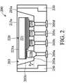
- FIG. 2is a schematic cross-sectional view illustrating another exemplary package system including an LED. Items of FIG. 2 that are the same items in FIG. 1 are indicated by the same reference numerals, increased by 100.
- a lens material 215can be disposed between a substrate 201 and an LED 220 and surround the LED 220 .
- the lens material 215may include color phosphor for adjusting the emission color from the LED 220 .
- a surface 215 a of the lens material 215can be over a surface 221 a of a transparent substrate 221 .
- the surface 215 acan be substantially level with a surface 201 a of the substrate 201 .
- a dome lens or dome encapsulant(not shown) can be disposed over the transparent substrate 221 , covering the LED 220 .
- the dome lensmay help to refract the light emitted from the LED 220 through the transparent substrate 221 .
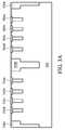
- FIGS. 3A-3Hare schematic cross-sectional views illustrating an exemplary method for forming a plurality of package systems. Items of FIGS. 3A-3H that are the same items in FIG. 1 are indicated by the same reference numerals, increased by 200 or 250.
- polymer materials 330 a - 330 ccan be formed in a substrate 302 .
- the polymer materials 330 a - 330 ccan be formed along scribe lines defined on the substrate 302 .
- the polymer materials 330 a - 330 ccan be formed by, for example, a single or multiple blade sawing processes or laser sawing processes for forming T-shape trenches in the substrate 302 .
- the polymer materials 330 a - 330 ccan be printed and/or dispensed in the T-shape trenches.
- the polymer materials 330 a - 330 ccan be then subjected to a curing process for hardening the polymer materials 330 a - 330 c.
- the thermally conductive structures 305 a - 305 d and 355 a - 355 dcan be formed by, for example, photolithographic and etch processes for forming openings in the substrate 302 .
- Conductive materialscan be formed in the openings by a CVD, PVD, ALD, electroplating method, and/or other process to fill the openings.
- a chemical mechanical polish (CMP) processcan polish the conductive materials over the substrate 302 , forming the thermally conductive structures 305 a - 305 d and 355 a - 355 d in the opening.
- a carrier 304e.g., a glass carrier, can be disposed over the substrate 302 .
- the carrier 304can be attached to the substrate 302 through an adhesive tape (not shown).
- the carrier 304can carry the substrate 302 for removing, e.g., polishing, a portion of the substrate 302 (shown in FIG. 3A ), forming substrates 301 and 351 .
- the removing processcan expose the polymer materials 330 a - 330 c .
- the polymer material 330 bcan isolate the substrate 301 from the substrate 351 .
- a plurality of grooves 311 a - 311 b and 311 c - 331 dcan be formed in the substrates 301 and 351 , respectively.
- the grooves 311 a - 311 dcan be formed adjacent to the polymer materials 330 a - 330 c .
- Each of the grooves 311 a - 311 dcan have beveled surfaces.
- the grooves 311 a - 311 dcan be formed by a bevel sawing process.
- tips of the grooves 311 a - 311 dcan be at the level substantially equal to the bottom surfaces of the thermally conductive structures 305 a - 305 d and 355 a - 355 d as shown in FIG. 3C .
- portions of the substrates 301 and 351can be removed for forming cavities 303 and 353 in the substrates 301 and 351 , respectively. Removing the portions of the substrates 301 and 351 can expose the thermally conductive structures 305 a - 305 d and 355 a - 355 d .
- the cavities 303 and 353can have flat surfaces 303 a and 353 a and beveled surfaces 303 b and 353 b , respectively.
- the beveled surfaces 303 b and 353 bcan serve as reflective surfaces for LEDs.
- removing the portions of the substrates 301 and 351can include a photolithographic process forming a patterned photoresist (not shown) exposing regions that are to be removed.
- An etch processe.g., a reactive ion etch (RIE) process, can remove the exposed regions.
- RIEreactive ion etch
- the thermally conductive structures 305 a - 305 d and 355 a - 355 dcan be optionally subjected to an electroless nickel immersion gold (ENIG) process or an immersion tin (Im—Sn) process for forming ENIG or Im—Sn material on the exposed surfaces of the thermally conductive structures 305 a - 305 d and 355 a - 355 d .
- ENIG or Im—Sn materialcan serve as a bonding interface between the thermally conductive structures 305 a - 305 d and 355 a - 355 d and 310 a - 310 d and 360 a - 360 d (shown in FIG. 3E ).
- LEDs 320 and 370can be disposed in the cavities 303 and 353 , respectively.
- the LEDs 320 and 370can be formed by any known LED fabricating method.
- the LEDs 320 and 370 including thermally conductive structures 310 a - 310 d and 360 a - 360 dcan be bonded with the thermally conductive structures 305 a - 305 d and 355 a - 355 d , respectively.
- the LEDs 320 and 370can be thermally and/or electrically coupled with the thermally conductive structures 305 a - 305 d and 355 a - 355 d through the thermally conductive structures 310 a - 310 d and 360 a - 360 d , respectively.
- lens materials 315 and 365can be formed between the substrate 301 and the LED 320 and between the substrate 351 and the LED 370 , respectively.
- the lens materials 315 and 365can be formed by printing or dispensing a lens material filling in the cavities 303 and 353 (shown in FIG. 3E ).
- a polish process and/or a plasma etch processcan be performed, removing the lens material over the transparent substrates 321 and 371 .
- the surface 315 a of the lens material 315can be substantially level with the surface 321 a of the transparent substrate 321 .
- a dome lens or dome encapsulant(not shown) can be formed over the transparent substrate 321 .
- the surface 315 a of the lens material 315can be formed over the surface 321 a of the transparent substrate 321 that is similar to the structure shown in FIG. 2 .
- the cavity 303 of the substrate 301(shown in FIG. 3E ) can be further deepened.
- the surface 321 a of the transparent substrateis lower than the surface 301 a of the substrate 301 .
- the lens material 315can be formed over the transparent substrate 321 and surround the LED 320 .
- the surface 315 a of the lens material 315can be substantially level with the surface 301 a of the substrate 301 .
- the structure shown in FIG. 3Fcan be flipped and mounted on a dicing tap 345 .
- the carrier 304can be removed from the substrates 301 and 351 .
- the structure shown in FIG. 3Gis subjected to a dicing process for separating the package system 300 from the package system 350 .
- the dicing processcan include a blade sawing process and/or a laser sawing process.
- the dicing processcan be performed along the polymer materials 330 a , 330 b , and 330 c .
- the polymer materials 330 a , 330 b , and 330 care disposed around the substrates 301 and 351 .
- the polymer materials 330 a , 330 b , and 330 ccan provide a desired mechanical support for singulation of the package systems 300 and 350 .
- the number of the package systems 300 and 350 formed by the processes described above in conjunction with FIGS. 3A-3Hare merely exemplary. More package systems including LEDs can be formed. Since multiple package systems can be formed on the same base substrate 302 (shown in FIG. 3A ), the processes described above in conjunction with FIGS. 3A-3H can be referred to as a wafer-level process.
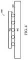
- FIG. 4is a schematic drawing illustrating a system including an exemplary LED package system disposed over a substrate board.
- a system 400can include a package system 402 disposed over a substrate board 401 .
- the substrate board 401can include a printed circuit board (PCB), a printed wiring board and/or other carrier that is capable of carrying an integrated circuit.
- the package system 402can be similar to the package system 100 or 200 described above in conjunction with FIGS. 1 and 2 .
- the package system 402can be electrically coupled with the substrate board 401 .
- the package system 402can be electrically and/or thermally coupled with the substrate board 401 through bumps 405 .
- the system 400can be part of an electronic system such as displays, panels, lighting systems, auto vehicles, entertainment devices, or the like.
- the system 400 including the package system 402can provides an entire system in one IC, so-called system on a chip (SOC) or system on integrated circuit (SOIC) devices.
- SOCsystem on a chip
- SOICsystem on integrated circuit
- an exemplary embodiment of this applicationprovides a package system.
- the package systemincludes a substrate having at least one first thermally conductive structure through the substrate. At least one second thermally conductive structure is disposed over the at least one first thermally conductive structure. At least one light-emitting diode (LED) is disposed over the at least one second thermally conductive structure.
- LEDlight-emitting diode
Landscapes
- Engineering & Computer Science (AREA)
- Computer Hardware Design (AREA)
- Microelectronics & Electronic Packaging (AREA)
- Power Engineering (AREA)
- Led Device Packages (AREA)
- Fastening Of Light Sources Or Lamp Holders (AREA)
Abstract
Description
Claims (19)
Priority Applications (4)
| Application Number | Priority Date | Filing Date | Title |
|---|---|---|---|
| US12/706,040US8390009B2 (en) | 2010-02-16 | 2010-02-16 | Light-emitting diode (LED) package systems |
| TW099115077ATWI482322B (en) | 2010-02-16 | 2010-05-12 | Packaging system |
| CN2010101834197ACN102163677A (en) | 2010-02-16 | 2010-05-18 | packaging system |
| US13/767,994US8628984B2 (en) | 2010-02-16 | 2013-02-15 | Light-emitting diode (LED) package systems |
Applications Claiming Priority (1)
| Application Number | Priority Date | Filing Date | Title |
|---|---|---|---|
| US12/706,040US8390009B2 (en) | 2010-02-16 | 2010-02-16 | Light-emitting diode (LED) package systems |
Related Child Applications (1)
| Application Number | Title | Priority Date | Filing Date |
|---|---|---|---|
| US13/767,994ContinuationUS8628984B2 (en) | 2010-02-16 | 2013-02-15 | Light-emitting diode (LED) package systems |
Publications (2)
| Publication Number | Publication Date |
|---|---|
| US20110198638A1 US20110198638A1 (en) | 2011-08-18 |
| US8390009B2true US8390009B2 (en) | 2013-03-05 |
Family
ID=44369030
Family Applications (2)
| Application Number | Title | Priority Date | Filing Date |
|---|---|---|---|
| US12/706,040Expired - Fee RelatedUS8390009B2 (en) | 2010-02-16 | 2010-02-16 | Light-emitting diode (LED) package systems |
| US13/767,994Expired - Fee RelatedUS8628984B2 (en) | 2010-02-16 | 2013-02-15 | Light-emitting diode (LED) package systems |
Family Applications After (1)
| Application Number | Title | Priority Date | Filing Date |
|---|---|---|---|
| US13/767,994Expired - Fee RelatedUS8628984B2 (en) | 2010-02-16 | 2013-02-15 | Light-emitting diode (LED) package systems |
Country Status (3)
| Country | Link |
|---|---|
| US (2) | US8390009B2 (en) |
| CN (1) | CN102163677A (en) |
| TW (1) | TWI482322B (en) |
Cited By (5)
| Publication number | Priority date | Publication date | Assignee | Title |
|---|---|---|---|---|
| US20120241793A1 (en)* | 2011-03-22 | 2012-09-27 | Seoul Opto Device Co., Ltd. | Light emitting diode package and method for manufacturing the same |
| US20130016477A1 (en)* | 2011-07-11 | 2013-01-17 | Texas Instruments Incorporated | Electronic Assembly Including Die on Substrate With Heat Spreader Having an Open Window on the Die |
| US20220028699A1 (en)* | 2020-07-21 | 2022-01-27 | Infineon Technologies Austria Ag | Chip-substrate composite semiconductor device |
| US20230395756A1 (en)* | 2022-06-01 | 2023-12-07 | Creeled, Inc. | Interconnect structures for improved light-emitting diode chip performance |
| US20240021594A1 (en)* | 2022-07-18 | 2024-01-18 | AUO Corporation | Micro led display device |
Families Citing this family (11)
| Publication number | Priority date | Publication date | Assignee | Title |
|---|---|---|---|---|
| US9293678B2 (en)* | 2010-07-15 | 2016-03-22 | Micron Technology, Inc. | Solid-state light emitters having substrates with thermal and electrical conductivity enhancements and method of manufacture |
| TW201312799A (en)* | 2011-09-02 | 2013-03-16 | Syue-Min Li | Light-emitting diode component |
| TWI490960B (en)* | 2012-01-17 | 2015-07-01 | Chipmos Technologies Inc | Semiconductor package structure and manufacturing method thereof |
| KR101932495B1 (en) | 2012-05-11 | 2018-12-27 | 삼성전자주식회사 | Semiconductor package and method of manufacturing the semiconductor package |
| US11213690B2 (en)* | 2012-06-15 | 2022-01-04 | Medtronic, Inc. | Wafer level packages of high voltage units for implantable medical devices |
| JP6325536B2 (en)* | 2012-07-05 | 2018-05-16 | コーニンクレッカ フィリップス エヌ ヴェKoninklijke Philips N.V. | Phosphor separated from LED by transparent spacer |
| DE102013111496A1 (en)* | 2013-10-18 | 2015-04-23 | Osram Opto Semiconductors Gmbh | Method for producing optoelectronic semiconductor components and optoelectronic semiconductor component |
| KR102102911B1 (en)* | 2013-11-29 | 2020-04-21 | 엘지디스플레이 주식회사 | Organic light emitting display device and manufacturing method of the same |
| US10734788B2 (en) | 2018-03-02 | 2020-08-04 | Cisco Technology, Inc. | Quantum dot lasers integrated on silicon submount with mechanical features and through-silicon vias |
| US10461495B2 (en) | 2018-03-02 | 2019-10-29 | Cisco Technology, Inc. | Substrate technology for quantum dot lasers integrated on silicon |
| US10734785B2 (en)* | 2018-03-02 | 2020-08-04 | Cisco Technology, Inc. | Silicon photonics co-integrated with quantum dot lasers on silicon |
Citations (31)
| Publication number | Priority date | Publication date | Assignee | Title |
|---|---|---|---|---|
| US5391917A (en) | 1993-05-10 | 1995-02-21 | International Business Machines Corporation | Multiprocessor module packaging |
| US5510298A (en) | 1991-09-12 | 1996-04-23 | Texas Instruments Incorporated | Method of interconnect in an integrated circuit |
| US5767001A (en) | 1993-05-05 | 1998-06-16 | Siemens Aktiengesellschaft | Process for producing semiconductor components between which contact is made vertically |
| US5998292A (en) | 1997-11-12 | 1999-12-07 | International Business Machines Corporation | Method for making three dimensional circuit integration |
| US6184060B1 (en) | 1996-10-29 | 2001-02-06 | Trusi Technologies Llc | Integrated circuits and methods for their fabrication |
| US6322903B1 (en) | 1999-12-06 | 2001-11-27 | Tru-Si Technologies, Inc. | Package of integrated circuits and vertical integration |
| US6448168B1 (en) | 1997-09-30 | 2002-09-10 | Intel Corporation | Method for distributing a clock on the silicon backside of an integrated circuit |
| US6465892B1 (en) | 1999-04-13 | 2002-10-15 | Oki Electric Industry Co., Ltd. | Interconnect structure for stacked semiconductor device |
| US6531328B1 (en)* | 2001-10-11 | 2003-03-11 | Solidlite Corporation | Packaging of light-emitting diode |
| US6538333B2 (en) | 2000-06-16 | 2003-03-25 | Chartered Semiconductor Manufacturing Ltd. | Three dimensional IC package module |
| US6599778B2 (en) | 2001-12-19 | 2003-07-29 | International Business Machines Corporation | Chip and wafer integration process using vertical connections |
| US20030189829A1 (en)* | 2001-08-09 | 2003-10-09 | Matsushita Electric Industrial Co., Ltd. | LED illumination apparatus and card-type LED illumination source |
| US6664129B2 (en) | 1996-10-29 | 2003-12-16 | Tri-Si Technologies, Inc. | Integrated circuits and methods for their fabrication |
| US6730533B2 (en)* | 2000-09-01 | 2004-05-04 | General Electric Company | Plastic packaging of LED arrays |
| US6800930B2 (en) | 2002-07-31 | 2004-10-05 | Micron Technology, Inc. | Semiconductor dice having back side redistribution layer accessed using through-silicon vias, and assemblies |
| US6841883B1 (en) | 2003-03-31 | 2005-01-11 | Micron Technology, Inc. | Multi-dice chip scale semiconductor components and wafer level methods of fabrication |
| US6924551B2 (en) | 2003-05-28 | 2005-08-02 | Intel Corporation | Through silicon via, folded flex microelectronic package |
| US6962872B2 (en) | 2002-12-09 | 2005-11-08 | International Business Machines Corporation | High density chip carrier with integrated passive devices |
| US7049170B2 (en) | 2003-12-17 | 2006-05-23 | Tru-Si Technologies, Inc. | Integrated circuits and packaging substrates with cavities, and attachment methods including insertion of protruding contact pads into cavities |
| US7060601B2 (en) | 2003-12-17 | 2006-06-13 | Tru-Si Technologies, Inc. | Packaging substrates for integrated circuits and soldering methods |
| US7071546B2 (en) | 2002-01-16 | 2006-07-04 | Alfred E. Mann Foundation For Scientific Research | Space-saving packaging of electronic circuits |
| US20060163596A1 (en)* | 2005-01-26 | 2006-07-27 | Gi-Cherl Kim | Two dimensional light source using light emitting diode and liquid crystal display device using the two dimensional light source |
| US7111149B2 (en) | 2003-07-07 | 2006-09-19 | Intel Corporation | Method and apparatus for generating a device ID for stacked devices |
| US7122912B2 (en) | 2004-01-28 | 2006-10-17 | Nec Electronics Corporation | Chip and multi-chip semiconductor device using thereof and method for manufacturing same |
| US7157787B2 (en) | 2002-02-20 | 2007-01-02 | Intel Corporation | Process of vertically stacking multiple wafers supporting different active integrated circuit (IC) devices |
| US7193308B2 (en) | 2003-09-26 | 2007-03-20 | Seiko Epson Corporation | Intermediate chip module, semiconductor device, circuit board, and electronic device |
| US20070145404A1 (en)* | 2005-12-27 | 2007-06-28 | Shinko Electric Industries Co., Ltd. | Semicondcutor device and manufacturing method of semiconductor device |
| US7262495B2 (en) | 2004-10-07 | 2007-08-28 | Hewlett-Packard Development Company, L.P. | 3D interconnect with protruding contacts |
| US7297574B2 (en) | 2005-06-17 | 2007-11-20 | Infineon Technologies Ag | Multi-chip device and method for producing a multi-chip device |
| US7335972B2 (en) | 2003-11-13 | 2008-02-26 | Sandia Corporation | Heterogeneously integrated microsystem-on-a-chip |
| US20080054486A1 (en)* | 2006-09-06 | 2008-03-06 | Shinko Electric Industries Co., Ltd. | Semiconductor device package, semiconductor apparatus, and methods for manufacturing the same |
Family Cites Families (4)
| Publication number | Priority date | Publication date | Assignee | Title |
|---|---|---|---|---|
| US20040188696A1 (en)* | 2003-03-28 | 2004-09-30 | Gelcore, Llc | LED power package |
| KR100649754B1 (en)* | 2005-10-31 | 2006-11-27 | 삼성전기주식회사 | Semiconductor device package |
| KR101381762B1 (en)* | 2007-09-28 | 2014-04-10 | 삼성전자주식회사 | Light emitting device |
| TW200921942A (en)* | 2007-11-14 | 2009-05-16 | Advanced Optoelectronic Tech | Packaging structure of light emitting diode device and method of fabricating the same |
- 2010
- 2010-02-16USUS12/706,040patent/US8390009B2/ennot_activeExpired - Fee Related
- 2010-05-12TWTW099115077Apatent/TWI482322B/ennot_activeIP Right Cessation
- 2010-05-18CNCN2010101834197Apatent/CN102163677A/enactivePending
- 2013
- 2013-02-15USUS13/767,994patent/US8628984B2/ennot_activeExpired - Fee Related
Patent Citations (39)
| Publication number | Priority date | Publication date | Assignee | Title |
|---|---|---|---|---|
| US5510298A (en) | 1991-09-12 | 1996-04-23 | Texas Instruments Incorporated | Method of interconnect in an integrated circuit |
| US5767001A (en) | 1993-05-05 | 1998-06-16 | Siemens Aktiengesellschaft | Process for producing semiconductor components between which contact is made vertically |
| US5391917A (en) | 1993-05-10 | 1995-02-21 | International Business Machines Corporation | Multiprocessor module packaging |
| US6639303B2 (en) | 1996-10-29 | 2003-10-28 | Tru-Si Technolgies, Inc. | Integrated circuits and methods for their fabrication |
| US6184060B1 (en) | 1996-10-29 | 2001-02-06 | Trusi Technologies Llc | Integrated circuits and methods for their fabrication |
| US6740582B2 (en) | 1996-10-29 | 2004-05-25 | Tru-Si Technologies, Inc. | Integrated circuits and methods for their fabrication |
| US6882030B2 (en) | 1996-10-29 | 2005-04-19 | Tru-Si Technologies, Inc. | Integrated circuit structures with a conductor formed in a through hole in a semiconductor substrate and protruding from a surface of the substrate |
| US6664129B2 (en) | 1996-10-29 | 2003-12-16 | Tri-Si Technologies, Inc. | Integrated circuits and methods for their fabrication |
| US6448168B1 (en) | 1997-09-30 | 2002-09-10 | Intel Corporation | Method for distributing a clock on the silicon backside of an integrated circuit |
| US5998292A (en) | 1997-11-12 | 1999-12-07 | International Business Machines Corporation | Method for making three dimensional circuit integration |
| US6472293B2 (en) | 1999-04-13 | 2002-10-29 | Oki Electric Industry Co., Ltd. | Method for manufacturing an interconnect structure for stacked semiconductor device |
| US6465892B1 (en) | 1999-04-13 | 2002-10-15 | Oki Electric Industry Co., Ltd. | Interconnect structure for stacked semiconductor device |
| US6693361B1 (en) | 1999-12-06 | 2004-02-17 | Tru-Si Technologies, Inc. | Packaging of integrated circuits and vertical integration |
| US6322903B1 (en) | 1999-12-06 | 2001-11-27 | Tru-Si Technologies, Inc. | Package of integrated circuits and vertical integration |
| US6538333B2 (en) | 2000-06-16 | 2003-03-25 | Chartered Semiconductor Manufacturing Ltd. | Three dimensional IC package module |
| US6730533B2 (en)* | 2000-09-01 | 2004-05-04 | General Electric Company | Plastic packaging of LED arrays |
| US20030189829A1 (en)* | 2001-08-09 | 2003-10-09 | Matsushita Electric Industrial Co., Ltd. | LED illumination apparatus and card-type LED illumination source |
| US6531328B1 (en)* | 2001-10-11 | 2003-03-11 | Solidlite Corporation | Packaging of light-emitting diode |
| US6599778B2 (en) | 2001-12-19 | 2003-07-29 | International Business Machines Corporation | Chip and wafer integration process using vertical connections |
| US7071546B2 (en) | 2002-01-16 | 2006-07-04 | Alfred E. Mann Foundation For Scientific Research | Space-saving packaging of electronic circuits |
| US7157787B2 (en) | 2002-02-20 | 2007-01-02 | Intel Corporation | Process of vertically stacking multiple wafers supporting different active integrated circuit (IC) devices |
| US6962867B2 (en) | 2002-07-31 | 2005-11-08 | Microntechnology, Inc. | Methods of fabrication of semiconductor dice having back side redistribution layer accessed using through-silicon vias and assemblies thereof |
| US7355273B2 (en) | 2002-07-31 | 2008-04-08 | Micron Technology, Inc. | Semiconductor dice having back side redistribution layer accessed using through-silicon vias, methods |
| US6800930B2 (en) | 2002-07-31 | 2004-10-05 | Micron Technology, Inc. | Semiconductor dice having back side redistribution layer accessed using through-silicon vias, and assemblies |
| US6962872B2 (en) | 2002-12-09 | 2005-11-08 | International Business Machines Corporation | High density chip carrier with integrated passive devices |
| US7030481B2 (en) | 2002-12-09 | 2006-04-18 | Internation Business Machines Corporation | High density chip carrier with integrated passive devices |
| US6841883B1 (en) | 2003-03-31 | 2005-01-11 | Micron Technology, Inc. | Multi-dice chip scale semiconductor components and wafer level methods of fabrication |
| US6924551B2 (en) | 2003-05-28 | 2005-08-02 | Intel Corporation | Through silicon via, folded flex microelectronic package |
| US7111149B2 (en) | 2003-07-07 | 2006-09-19 | Intel Corporation | Method and apparatus for generating a device ID for stacked devices |
| US7193308B2 (en) | 2003-09-26 | 2007-03-20 | Seiko Epson Corporation | Intermediate chip module, semiconductor device, circuit board, and electronic device |
| US7335972B2 (en) | 2003-11-13 | 2008-02-26 | Sandia Corporation | Heterogeneously integrated microsystem-on-a-chip |
| US7060601B2 (en) | 2003-12-17 | 2006-06-13 | Tru-Si Technologies, Inc. | Packaging substrates for integrated circuits and soldering methods |
| US7049170B2 (en) | 2003-12-17 | 2006-05-23 | Tru-Si Technologies, Inc. | Integrated circuits and packaging substrates with cavities, and attachment methods including insertion of protruding contact pads into cavities |
| US7122912B2 (en) | 2004-01-28 | 2006-10-17 | Nec Electronics Corporation | Chip and multi-chip semiconductor device using thereof and method for manufacturing same |
| US7262495B2 (en) | 2004-10-07 | 2007-08-28 | Hewlett-Packard Development Company, L.P. | 3D interconnect with protruding contacts |
| US20060163596A1 (en)* | 2005-01-26 | 2006-07-27 | Gi-Cherl Kim | Two dimensional light source using light emitting diode and liquid crystal display device using the two dimensional light source |
| US7297574B2 (en) | 2005-06-17 | 2007-11-20 | Infineon Technologies Ag | Multi-chip device and method for producing a multi-chip device |
| US20070145404A1 (en)* | 2005-12-27 | 2007-06-28 | Shinko Electric Industries Co., Ltd. | Semicondcutor device and manufacturing method of semiconductor device |
| US20080054486A1 (en)* | 2006-09-06 | 2008-03-06 | Shinko Electric Industries Co., Ltd. | Semiconductor device package, semiconductor apparatus, and methods for manufacturing the same |
Cited By (11)
| Publication number | Priority date | Publication date | Assignee | Title |
|---|---|---|---|---|
| US20120241793A1 (en)* | 2011-03-22 | 2012-09-27 | Seoul Opto Device Co., Ltd. | Light emitting diode package and method for manufacturing the same |
| US10074778B2 (en)* | 2011-03-22 | 2018-09-11 | Seoul Viosys Co., Ltd. | Light emitting diode package and method for manufacturing the same |
| US10727376B2 (en) | 2011-03-22 | 2020-07-28 | Seoul Viosys Co., Ltd. | Light emitting diode package and method of manufacturing the same |
| US11563152B2 (en) | 2011-03-22 | 2023-01-24 | Seoul Viosys Co., Ltd. | Light emitting diode package and method of manufacturing the same |
| US12107195B2 (en) | 2011-03-22 | 2024-10-01 | Seoul Viosys Co., Ltd. | Light emitting diode package and method of manufacturing the same |
| US20130016477A1 (en)* | 2011-07-11 | 2013-01-17 | Texas Instruments Incorporated | Electronic Assembly Including Die on Substrate With Heat Spreader Having an Open Window on the Die |
| US8526186B2 (en)* | 2011-07-11 | 2013-09-03 | Texas Instruments Incorporated | Electronic assembly including die on substrate with heat spreader having an open window on the die |
| US20220028699A1 (en)* | 2020-07-21 | 2022-01-27 | Infineon Technologies Austria Ag | Chip-substrate composite semiconductor device |
| US12368052B2 (en)* | 2020-07-21 | 2025-07-22 | Infineon Technologies Austria Ag | Chip-substrate composite semiconductor device |
| US20230395756A1 (en)* | 2022-06-01 | 2023-12-07 | Creeled, Inc. | Interconnect structures for improved light-emitting diode chip performance |
| US20240021594A1 (en)* | 2022-07-18 | 2024-01-18 | AUO Corporation | Micro led display device |
Also Published As
| Publication number | Publication date |
|---|---|
| CN102163677A (en) | 2011-08-24 |
| TW201130176A (en) | 2011-09-01 |
| US8628984B2 (en) | 2014-01-14 |
| US20110198638A1 (en) | 2011-08-18 |
| TWI482322B (en) | 2015-04-21 |
| US20130157395A1 (en) | 2013-06-20 |
Similar Documents
| Publication | Publication Date | Title |
|---|---|---|
| US8390009B2 (en) | Light-emitting diode (LED) package systems | |
| US8183578B2 (en) | Double flip-chip LED package components | |
| US8399269B2 (en) | LED flip-chip package structure with dummy bumps | |
| US20250056937A1 (en) | Etched trenches in bond materials for die singulation, and associated systems and methods | |
| US12199082B2 (en) | Method of direct-bonded optoelectronic devices | |
| US9362474B2 (en) | Vertical LED chip package on TSV carrier | |
| US9502627B2 (en) | Wafer level photonic devices dies structure and method of making the same | |
| US20110198609A1 (en) | Light-Emitting Devices with Through-Substrate Via Connections | |
| US8183580B2 (en) | Thermally-enhanced hybrid LED package components | |
| US8754440B2 (en) | Light-emitting diode (LED) package systems and methods of making the same | |
| US20120313115A1 (en) | Light emitter device packages, modules and methods | |
| JP2017502524A (en) | Wavelength conversion type semiconductor light emitting device | |
| US8598611B2 (en) | Vertical solid-state transducers and solid-state transducer arrays having backside terminals and associated systems and methods | |
| JP2015514319A (en) | Encapsulated semiconductor light emitting device | |
| CN100442554C (en) | Light emitting diode and manufacturing method thereof | |
| Wang et al. | Wafer level LED packaging with optimal light output and thermal dissipation for high-brightness lighting |
Legal Events
| Date | Code | Title | Description |
|---|---|---|---|
| AS | Assignment | Owner name:TAIWAN SEMICONDUCTOR MANUFACTURING COMPANY. LTD., Free format text:ASSIGNMENT OF ASSIGNORS INTEREST;ASSIGNOR:WANG, CHUNG YU;REEL/FRAME:024199/0083 Effective date:20100308 | |
| AS | Assignment | Owner name:TSMC SOLID STATE LIGHTING LTD., TAIWAN Free format text:ASSIGNMENT OF ASSIGNORS INTEREST;ASSIGNOR:TAIWAN SEMICONDUCTOR MANUFACTURING COMPANY LTD.;REEL/FRAME:027854/0363 Effective date:20120301 | |
| STCF | Information on status: patent grant | Free format text:PATENTED CASE | |
| AS | Assignment | Owner name:EPISTAR CORPORATION, TAIWAN Free format text:MERGER;ASSIGNOR:CHIP STAR LTD.;REEL/FRAME:037160/0212 Effective date:20150715 Owner name:CHIP STAR LTD., TAIWAN Free format text:CHANGE OF NAME;ASSIGNOR:TSMC SOLID STATE LIGHTING LTD.;REEL/FRAME:037160/0198 Effective date:20150402 | |
| FPAY | Fee payment | Year of fee payment:4 | |
| FEPP | Fee payment procedure | Free format text:MAINTENANCE FEE REMINDER MAILED (ORIGINAL EVENT CODE: REM.); ENTITY STATUS OF PATENT OWNER: LARGE ENTITY | |
| LAPS | Lapse for failure to pay maintenance fees | Free format text:PATENT EXPIRED FOR FAILURE TO PAY MAINTENANCE FEES (ORIGINAL EVENT CODE: EXP.); ENTITY STATUS OF PATENT OWNER: LARGE ENTITY | |
| STCH | Information on status: patent discontinuation | Free format text:PATENT EXPIRED DUE TO NONPAYMENT OF MAINTENANCE FEES UNDER 37 CFR 1.362 | |
| FP | Lapsed due to failure to pay maintenance fee | Effective date:20210305 |