US8385158B1 - Method and system for providing a magnetic recording transducer having a planarized near-field transducer and a sloped pole - Google Patents
Method and system for providing a magnetic recording transducer having a planarized near-field transducer and a sloped poleDownload PDFInfo
- Publication number
- US8385158B1 US8385158B1US12/574,621US57462109AUS8385158B1US 8385158 B1US8385158 B1US 8385158B1US 57462109 AUS57462109 AUS 57462109AUS 8385158 B1US8385158 B1US 8385158B1
- Authority
- US
- United States
- Prior art keywords
- providing
- planarized
- nft
- mask
- line
- Prior art date
- Legal status (The legal status is an assumption and is not a legal conclusion. Google has not performed a legal analysis and makes no representation as to the accuracy of the status listed.)
- Active, expires
Links
- 238000000034methodMethods0.000titleclaimsabstractdescription47
- 239000012212insulatorSubstances0.000claimsdescription55
- 238000000151depositionMethods0.000claimsdescription19
- 238000005253claddingMethods0.000claimsdescription12
- 125000006850spacer groupChemical group0.000claimsdescription5
- 239000000126substanceSubstances0.000claimsdescription2
- IYLGZMTXKJYONK-ACLXAEORSA-N(12s,15r)-15-hydroxy-11,16-dioxo-15,20-dihydrosenecionan-12-yl acetateChemical compoundO1C(=O)[C@](CC)(O)C[C@@H](C)[C@](C)(OC(C)=O)C(=O)OCC2=CCN3[C@H]2[C@H]1CC3IYLGZMTXKJYONK-ACLXAEORSA-N0.000description13
- IYLGZMTXKJYONK-UHFFFAOYSA-NruwenineNatural productsO1C(=O)C(CC)(O)CC(C)C(C)(OC(C)=O)C(=O)OCC2=CCN3C2C1CC3IYLGZMTXKJYONK-UHFFFAOYSA-N0.000description13
- 230000015572biosynthetic processEffects0.000description11
- TWNQGVIAIRXVLR-UHFFFAOYSA-Noxo(oxoalumanyloxy)alumaneChemical compoundO=[Al]O[Al]=OTWNQGVIAIRXVLR-UHFFFAOYSA-N0.000description9
- 239000000463materialSubstances0.000description8
- NJPPVKZQTLUDBO-UHFFFAOYSA-NnovaluronChemical compoundC1=C(Cl)C(OC(F)(F)C(OC(F)(F)F)F)=CC=C1NC(=O)NC(=O)C1=C(F)C=CC=C1FNJPPVKZQTLUDBO-UHFFFAOYSA-N0.000description8
- 238000004519manufacturing processMethods0.000description7
- 229910052751metalInorganic materials0.000description3
- 239000002184metalSubstances0.000description3
- 230000003287optical effectEffects0.000description3
- 229920002120photoresistant polymerPolymers0.000description3
- 230000008021depositionEffects0.000description2
- 238000010438heat treatmentMethods0.000description2
- 239000000696magnetic materialSubstances0.000description2
- BPUBBGLMJRNUCC-UHFFFAOYSA-Noxygen(2-);tantalum(5+)Chemical compound[O-2].[O-2].[O-2].[O-2].[O-2].[Ta+5].[Ta+5]BPUBBGLMJRNUCC-UHFFFAOYSA-N0.000description2
- 230000002411adverseEffects0.000description1
- PNEYBMLMFCGWSK-UHFFFAOYSA-Naluminium oxideInorganic materials[O-2].[O-2].[O-2].[Al+3].[Al+3]PNEYBMLMFCGWSK-UHFFFAOYSA-N0.000description1
- 229910052593corundumInorganic materials0.000description1
- 230000003247decreasing effectEffects0.000description1
- 150000002500ionsChemical class0.000description1
- 229910001936tantalum oxideInorganic materials0.000description1
- 229910001845yogo sapphireInorganic materials0.000description1
Images


Classifications
- G—PHYSICS
- G11—INFORMATION STORAGE
- G11B—INFORMATION STORAGE BASED ON RELATIVE MOVEMENT BETWEEN RECORD CARRIER AND TRANSDUCER
- G11B5/00—Recording by magnetisation or demagnetisation of a record carrier; Reproducing by magnetic means; Record carriers therefor
- G11B5/127—Structure or manufacture of heads, e.g. inductive
- G11B5/31—Structure or manufacture of heads, e.g. inductive using thin films
- G11B5/3163—Fabrication methods or processes specially adapted for a particular head structure, e.g. using base layers for electroplating, using functional layers for masking, using energy or particle beams for shaping the structure or modifying the properties of the basic layers
- G—PHYSICS
- G11—INFORMATION STORAGE
- G11B—INFORMATION STORAGE BASED ON RELATIVE MOVEMENT BETWEEN RECORD CARRIER AND TRANSDUCER
- G11B5/00—Recording by magnetisation or demagnetisation of a record carrier; Reproducing by magnetic means; Record carriers therefor
- G11B2005/0002—Special dispositions or recording techniques
- G11B2005/0005—Arrangements, methods or circuits
- G11B2005/0021—Thermally assisted recording using an auxiliary energy source for heating the recording layer locally to assist the magnetization reversal
- G—PHYSICS
- G11—INFORMATION STORAGE
- G11B—INFORMATION STORAGE BASED ON RELATIVE MOVEMENT BETWEEN RECORD CARRIER AND TRANSDUCER
- G11B5/00—Recording by magnetisation or demagnetisation of a record carrier; Reproducing by magnetic means; Record carriers therefor
- G11B5/48—Disposition or mounting of heads or head supports relative to record carriers ; arrangements of heads, e.g. for scanning the record carrier to increase the relative speed
- G11B5/58—Disposition or mounting of heads or head supports relative to record carriers ; arrangements of heads, e.g. for scanning the record carrier to increase the relative speed with provision for moving the head for the purpose of maintaining alignment of the head relative to the record carrier during transducing operation, e.g. to compensate for surface irregularities of the latter or for track following
- G11B5/60—Fluid-dynamic spacing of heads from record-carriers
- G11B5/6005—Specially adapted for spacing from a rotating disc using a fluid cushion
- G11B5/6088—Optical waveguide in or on flying head
Definitions
- FIG. 1depicts a portion of a conventional energy assisted magnetic recording (EAMR) transducer 10 .
- the conventional EAMR transducer 10is used in writing to recording media 30 . To do so, the conventional EAMR transducer 10 receives light, or energy, from a conventional laser (not shown in FIG. 1 ). Also shown is grating 20 .
- the conventional EAMR transducer 10includes a conventional waveguide 12 , conventional pole 14 , and a conventional near-field transducer (NFT) 16 . Also shown is a laser spot 22 on the gratings 20 . Other components that may be part of the conventional EAMR transducer 10 are not shown.
- the light from the spot 22 on the grating 20is coupled to the conventional waveguide 12 .
- the conventional waveguide 12guides the light to the conventional NFT 16 near the air-bearing surface (ABS).
- the conventional NFT 16focuses the energy from the waveguide 12 to an optical spot 32 on the media 30 .
- a small region of the conventional media 30is heated by the spot 32 . This region becomes more magnetically soft.
- the conventional EAMR transducer 10magnetically writes data to the heated region of the recording media by energizing the conventional pole 14 .
- the conventional EAMR transducer 10may function, there are drawbacks.
- the size of the conventional NFT 16is desired to be small in order to limit the size of the spot 32 .
- the distances between the pole 14 and the conventional NFT 16 and between the conventional NFT 16 and the media 30are desired to be carefully controlled.
- caremust be taken in ensuring that the conventional pole 14 and conventional waveguide 12 are sufficiently separated that the magnetic field of the conventional pole 14 does not adversely affect the optical performance of the conventional waveguide 12 . Fabrication of a conventional EAMR transducer 10 that takes these factors into consideration may be problematic.
- a method and system for fabricating an energy assisted magnetic recording (EAMR) transduceris described.
- the EAMR transducerhas an air-bearing surface (ABS) and a waveguide.
- the methodincludes providing a planarized near-field transducer (NFT) for the waveguide and forming a sloped surface on the planarized NFT.
- the sloped surfacehas a front edge separated from the ABS by a distance.
- the method and systemalso include providing a write pole on the sloped surface.
- FIG. 1is depicts a conventional EAMR transducer.
- FIG. 2is a flow chart depicting an exemplary embodiment of a method for fabricating an EAMR transducer.
- FIG. 3depicts a side view of an exemplary embodiment of a magnetic recording transducer.
- FIG. 4is a flow chart depicting another exemplary embodiment of a method for fabricating a magnetic recording transducer.
- FIGS. 5-23depicts plan and ABS views of an exemplary embodiment of an EAMR transducer during fabrication.
- FIG. 2is an exemplary embodiment of a method 100 for providing an EAMR transducer. For simplicity, some steps may be omitted.
- the method 100is also described in the context of providing a single EAMR transducer. However, the method 100 may be used to fabricate multiple transducers at substantially the same time.
- the method 100is also described in the context of particular structures. A structure or layer may include multiple materials and/or multiple sub-layers and may be formed using multiple sub-steps.
- the method 100also may start after formation of other portions of the EAMR transducer. For example, the method 100 may commence after formation of a read transducer. In addition, the method may start after formation of portions of the EAMR transducer. For example, a return pole and at least a portion of the waveguide may have been formed.
- a planarized NFT for the waveguideis provided, via step 102 .
- a planarized NFTis an NFT having its top surface substantially coplanar with a remaining portion of the transducer.
- the planarized NFThas an insulator such as aluminum oxide adjacent to its sides.
- the top of the planarized NFTmay be substantially coplanar with the insulator.
- Step 102may include multiple substeps.
- the planarized NFTmay include a line portion and a pad portion. Further, during formation, an anchor portion may also be formed, then later removed.
- step 102may include providing the line-portion proximate to the location at which the ABS is to be formed and providing an insulator adjoining the line-portion of the planarized NFT.
- This processmay be carried out such that the insulator top is substantially coplanar with the top of the line-potion of the planarized NFT.
- the insulatoris part of a cladding of the waveguide.
- its formationmay be accomplished using an isolated line (iso-line) mask.
- the line portionmay be formed by depositing a substantially flat metallic layer, providing an iso-line mask on the metallic layer, and removing an exposed portion of the metallic layer.
- the iso-line maskincludes an isolated line corresponding to a line-portion of the planarized NFT.
- step 102may also include forming the pad portion of the planarized NFT. Formation of the pad portion may include providing a mask having an aperture covering at least part of the line portion of the planarized NFT, removing a portion of the planarized NFT exposed by the aperture, and providing an additional metallic layer. A portion of the additional metallic layer in the aperture forms the pad portion of the planarized NFT. Thus, once a lift-off or other mechanism for removing the mask is completed, the pad portion of the planarized NFT is formed.
- a sloped surfaceis formed on the planarized NFT, via step 104 .
- the sloped surfacehas a front edge separated from the ABS by a distance. This distance may vary depending upon the particular implementation.
- the sloped surfacemakes an angle of at least twenty-five and not more than sixty-five degrees with normal to the ABS. In one such embodiment, the sloped surface makes an angle of approximately forty-five degrees with normal to the ABS. In some such embodiments, this angle is at least forty degrees and not more than fifty degrees.
- the sloped surfaceis provided by depositing a flat spacer layer, forming an undercut mask having an aperture therein, and then depositing a nonmagnetic material with the undercut mask in place. The undercut mask allows for less deposition of material under the undercut. Thus, the material deposited forms a sloped surface. In other embodiment, directional deposition and/or other methods may be used to form the sloped surface.
- a write poleis provided on the sloped surface, via step 106 .
- a portion of the write poleis sloped.
- the portion of the write pole within the distance from the ABSis substantially flat. This distance may be on the order of fifty to two hundred fifty nanometers.
- Step 106may include depositing a stop layer a portion of which is on the sloped surface, then depositing a nonmagnetic layer.
- the nonmagnetic layermay be an insulating layer.
- the insulating layerforms part of the cladding for the waveguide of the EAMR transducer.
- a trenchmay then be formed proximate to the ABS in the insulating layer.
- the trenchmay be formed by removing a portion of the insulating layer on the sloped surface using a process that terminates on the stop layer.
- the write polemay be deposited such that a portion of the write pole resides in the trench.
- the trench in the insulating layermay be formed by planarizing the insulating layer, depositing a hard mask layer on the insulating layer, and providing a pole mask that has an aperture over the sloped surface. This aperture corresponds to the trench and thus to the pole.
- the pattern of the pole maskis then transferred to the hard mask layer to form a hard mask.
- the pole maskmay be removed and the trench is etched in the insulating layer.
- the hard mask and a portion of the stop layerare removed before a magnetic layer for the pole is deposited. This pole layer may then be planarized to form the pole.
- FIG. 3depicts a side view of an exemplary embodiment of a magnetic recording transducer 110 that may be formed using the method 100 .
- the EAMR transducer 110may reside on a slider and be part of a merged head including a read transducer.
- the EAMR transducer 110may be used in an EAMR disk drive including read transducer(s).
- the EAMR transducer 110has an ABS configured to reside in proximity to the media (not shown in FIG. 3 ) during use of the EAMR transducer 110 .
- the EAMR transducer 110includes coils 112 and 114 , a waveguide 120 , and a pole 130 .
- the EAMR transducer 110also includes a planarized NFT 116 .
- the coils 112 and 114are for energizing the pole 130 .
- Energy from a laser or other analogous energy source(not shown) is coupled to the waveguide 120 through the grating(s) (not shown).
- the waveguide 120directs energy toward the ABS.
- the waveguide 120includes a mirror 122 , cladding 124 and 128 , as well as a core 126 .
- the waveguide 120may include other and/or different components.
- the pole 130includes a write pole 132 , a yoke 134 , a back pedestal 140 , and return pole portions 136 and 138 .
- the write pole tip 132is coupled to the back pedestal 140 through the yoke 134 .
- the waveguide 120passes through the back pedestal 140 , which may thus includes apertures (not shown) therein.
- the waveguidemay be direct energy to the planarized NFT 116 in another manner.
- Formation of many portions of the EAMR transducer 110such as coils 112 and 114 , return pole portions 136 and 138 , back pedestal 140 , waveguide 120 and yoke 134 are not discussed in the method 100 . Thus, these portions of the EAMR transducer 110 may be formed before, after, interleaved with and/or in conjunction with the steps of the method 100 .
- the EAMR transducer 110includes planarized NFT 116 having a top that is substantially coplanar with the top of the cladding/insulator 127 . This planarized NFT 116 may be formed using the method 100 . Further, the EAMR transducer 110 includes sloped surface 129 on which the write pole tip 132 is formed. The sloped surface 129 is a surface of insulator 133 . In some embodiments, the insulator 133 is aluminum oxide.
- the planarized NFT 116In operation, light from the laser is provided to the grating, then the waveguide 120 .
- the planarized NFT 116further focuses the energy onto a small spot on the media, heating, and a small region of the media.
- the coils 112 and 114energize the write pole 132 while the media is heated.
- the write pole 132may write data to the media.
- fabricating and performance of the EAMR transducer 110may be improved.
- a smaller optical spotmay be provided by the EAMR transducer.
- an iso-line maskis used in forming the line portion of the planarized NFT 116 , a very narrow planarized NFT 116 may be fabricated.
- a smaller spot size and, therefore, higher density tracksmay thus be achieved.
- the planarized NFT 116is substantially co-planar with adjoining structures, a substantially planar surface is formed. Therefore, manufacturing of subsequent layers, including the sloped surface 129 , may be facilitated. Further, the bottom portion of the write pole 132 proximate to the ABS is substantially flat and thus equidistant from the planarized NFT 116 .
- the sloped surface 129allows the bottom surface of the write pole 132 further from the ABS to be a greater distance from the waveguide 120 .
- the magnetic field in the write pole 132may be less likely to interfere with performance of the optics in the waveguide 120 . Consequently, performance of the waveguide 120 and thus the EAMR transducer 110 may be improved.
- FIG. 4is a flow chart depicting another exemplary embodiment of a method 150 for fabricating a magnetic recording transducer.
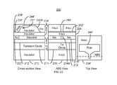
- FIGS. 5-23each depict cross section, ABS and plan views of an exemplary embodiment of an EAMR transducer 200 during fabrication. Note that the ABS view is taken at the location of the ABS, marked by dashed line in the top view in FIGS. 5-23 .
- the method 150is also described in the context of particular structures. A structure or layer may include multiple materials and/or multiple sub-layers. Structures may be formed using multiple sub-steps.
- the method 150also may start after formation of other portions of the EAMR transducer. For example, the method 150 may commence after formation of a read transducer.
- the methodmay start after formation of portions of the EAMR transducer 200 .
- a return pole and at least a portion of the waveguidemay have been formed.
- only a portion of the EAMR transducer 200is shown.
- stepsmay be omitted or combined in the method 150 .
- a metallic layersuch as Au is deposited, via step 152 .
- other layerssuch as tantalum oxide (Ta 2 O 5 ) and aluminum oxide (e.g. Al 2 O 3 ) have also been deposited. These layers may form part of the waveguide.
- An iso-line maskis provided on the metallic layer, via step 154 .
- the iso-line mask provided in step 154is typically a photoresist mask.
- the iso-line maskincludes an isolated line that corresponds to a line-portion of the planarized NFT proximate to the ABS.
- FIG. 5depicts the EAMR transducer 200 after step 154 is performed. Thus, underlying aluminum oxide layer 210 , tantalum oxide layer 212 , insulating layer 213 , and metal layer 214 are shown. In some embodiments, the metal layer 214 is Au. Also shown is iso-line mask 216 .
- the iso-line mask 216includes a line portion 216 A and an anchor portion 216 B. The anchor portion 216 B is generally not present in the final device. Instead, portions of the wafer are lapped and/or otherwise removed to expose the ABS.
- the pattern of the iso-line mask 216is then transferred to the metallic layer 214 , via step 156 .
- Step 156is carried out by removing an exposed portion of the metallic layer 216 .
- FIG. 6depicts the EAMR transducer 200 after step 214 is performed. Thus, a portion of the metallic layer 214 has been removed, leaving metallic structure 214 A and 214 B. The remaining portion of the metallic layer 214 has a line portion 214 A and an anchor portion 214 B. The line-portion 214 A of the planarized NFT is proximate to the ABS;
- FIG. 7depicts the EAMR transducer 200 after step 158 is performed. Consequently, insulator 218 is shown. The insulator 218 covers the top of the EAMR transducer 200 . Consequently, the location of the iso-line mask 216 is shown by dotted lines in the top view of FIG. 7 . A portion of the insulator 216 adjoins the line portion 214 A of the planarized NFT. The iso-line mask 216 may be removed, via step 160 . Also in step 160 , a low pressure and/or brief planarization may be performed.
- FIG. 8depicts the EAMR transducer 200 after step 160 is performed.
- the portion 218 ′ of the insulator adjacent to the metal 214 A and 214 Bremains.
- the top of the line portion 214 A of the planarized NFTis substantially coplanar with the insulator 218 ′.
- the top of the anchor portion 214 Bis also substantially coplanar with the top of the insulator 218 ′.
- the insulator 218 ′forms a portion of the cladding of the waveguide.
- steps 152 - 160the line portion 214 A of the planarized NFT is provided.
- FIG. 9depicts the EAMR transducer 200 after step 162 is performed.
- pad portion mask 220is shown.
- the pad portion mask 220is a photoresist mask.
- the pad portion mask 220includes aperture 221 .
- the aperture 221is triangle shaped. However, other shapes may be used for the pad.
- Part of the line portion 214 A of the planarized NFTmay be exposed by the aperture 221 .
- the pattern of the pad portion mask 110is transferred to the transducer 200 , via step 164 .
- FIG. 10depicts the transducer 200 after step 164 is performed.
- the exposed portion of the metallic layer 214 ′ and insulator 218 ′have been substantially removed.
- remaining portion of the insulator 218 ′′ and line portion 214 A′ of the planarized NFTare shown. In some embodiments, all of the exposed line portion 214 A′ would be removed.
- FIG. 11depicts the EAMR transducer 200 after step 168 is performed.
- metallic layer 222is shown.
- a portion of the metallic layer 222resides in the aperture 221 . Consequently, the aperture 221 is shown as a dotted line in the top view of FIG. 11 .
- the pad portion mask 220is removed, via step 168 .
- a lift offis performed.
- FIG. 12depicts the EAMR transducer 200 after step 168 is performed.
- the line portion 214 A′ of the NFT and the pad portion 222 ′ of the planarized NFTare shown.
- Steps 162 - 168may be viewed as forming the pad portion of the planarized NFT.
- Anchor portion 214 Bis also depicted.
- the planarized NFT 223 including pad portion 222 ′ and line portion 2134 ′is fabricated. As can be seen in FIG.
- step 152 - 168may be viewed as forming the planarized NFT 223 .
- an insulatoris deposited, via step 170 .
- aluminum oxideis deposited in step 170 .
- FIG. 13depicts the EAMR transducer 200 after step 170 is performed.
- insulator 224is provided.
- the line portion 214 A′ and pad portion 222 ′are not labeled. Instead, planarized NFT 223 is labeled.
- the insulator 224is aluminum oxide. A portion of the insulator acts as a spacer between the planarized NFT 223 and the write pole to be formed. In some embodiments, the insulator 224 is at least ten and not more than fifty nanometers thick.
- Step 172may include forming a bilayer photoresist mask.
- FIG. 14depicts the EAMR transducer 200 after step 172 is performed.
- undercut mask 226has been formed.
- the undercut mask 226includes a lower portion 226 A and an upper portion 226 B.
- the lower portion 226 A and upper portion 226 Bare formed by different layers of a bilayer mask.
- the undercut mask 226includes aperture 228 .
- the lower portion 226 Aextends a depth, d from the ABS.
- the upper portion 226 Bextends farther from the ABS, forming undercut 227 .
- the undercut mask 226may be configured substantially as desired.
- step 174includes depositing a layer of aluminum oxide.
- FIG. 15depicts the EAMR transducer 200 after step 174 is performed.
- undercut 227is not labeled.
- insulating layer 230is provided. A portion of the insulator 230 A resides in the aperture 228 . Because of the presence of the undercut mask 226 , the insulator 230 A naturally forms the sloped surface 231 . More specifically, the insulator 230 A has a front, sloped surface 231 . Because of the bottom portion 226 A of the undercut mask 226 , the front of the insulator 230 A is separated from the ABS by the distance, d. In some embodiments, the insulator 230 A is part of the cladding of the waveguide (not separately labeled).
- FIG. 16depicts the transducer after step 176 is performed.
- the insulator 230 A having sloped surface 231is formed.
- the front of the sloped surface 231is separated from the ABS by the distance d.
- steps 170 - 176may be considered to form the insulator 230 A having the sloped surface 231 .
- step 178includes providing a mask with an aperture over the portion of the EAMR transducer 200 on which the stop layer is desired. The stop layer may then be deposited and the mask removed, for example using a lift off process.
- FIG. 17depicts the transducer 200 after step 178 is performed.
- a stop layer 232is formed on the sloped surface 231 .
- the stop layer 232includes materials such as Ru, which are insensitive to an etch that removes the insulator 230 A.
- the stop layermay also function as a seed layer for the pole being formed.
- the stop layeris 25-30 nm thick.
- Step 180may include depositing an insulating layer such as an aluminum oxide layer, then planarizing the EAMR transducer 200 . The planarization step continues until a portion of the stop layer 232 at the top of the insulator 230 A is exposed.
- FIG. 18depicts the transducer after step 180 is performed. Thus, insulator 234 is shown. Further, a portion of the stop layer 232 on insulator 230 A may be exposed.
- a hard mask layeris provided, via step 182 .
- formation of the hard mask layer 182includes blanket depositing a material, such as Ru, which is insensitive to an etch that removes the insulator 234 .
- a mask having an aperture over the region in which the pole is to be formedis provided, via step 184 .
- FIG. 19depicts the transducer 200 after step 184 is performed.
- hard mask layer 236 and mask 238are shown.
- the mask 238includes aperture 240 . This aperture 240 has the desired size of the pole and is aligned with the region in which the pole is to be formed.
- FIG. 20depicts the transducer after step 186 is performed.
- hard mask 236 ′is shown.
- a trench in the insulator 234is formed, via step 188 .
- Step 188includes performing an etch, such as a reactive ion etch capable of removing insulator 234 .
- the mask 238may be removed.
- FIG. 21depicts the transducer 200 after step 188 is performed.
- trench 242 in insulator 234 ′is shown. The trench 242 is configured to fit the desired profile and location of the bottom surface of a pole.
- the hard mask 236 ′is removed, via step 190 .
- the pole material(s)are provided, via step 192 .
- Step 192may include depositing a seed layer in addition to depositing magnetic material(s) for the pole.
- FIG. 22depicts the transducer 200 after step 190 is performed. Magnetic material(s) 244 are thus shown. For clarity, trench 242 is not labeled. Portions of the layer 232 have been removed, leaving stop layer 232 ′.
- the transducermay then be planarized, via step 194 .
- a CMPmay be performed.
- FIG. 23depicts the transducer 200 after step 194 is performed.
- pole 244 ′has been formed. Additional portions of the pole 244 ′ as well as other part of the EAMR transducer 200 may also be formed. For example, a yoke, portions of the back gap, and/or other structures may be fabricated.
- the transducer 200is typically lapped or otherwise polished so that the front of the pole 244 ′ is at the ABS.
- the transducer 200may be formed. Because the iso-line mask 216 ′ is used in forming the line portion of the planarized NFT 223 , a very narrow planarized NFT 223 may be fabricated. A smaller spot size and, therefore, higher density tracks may thus be achieved. Because the planarized NFT 223 is substantially co-planar with adjoining structures, a substantially planar surface is formed. Thus, damage to the planarized NFT 223 may be less likely. Further, manufacturing of subsequent layers, including the sloped surface 129 , may be facilitated. Because it is formed on the sloped surface 231 , the bottom surface of the write pole 244 ′ is farther from the waveguide.
- the magnetic field in the write pole 244 ′may be less likely to interfere with performance of the optics in the waveguide.
- the portion of the pole 244 ′ proximate to the ABSis substantially flat and a substantially constant distance from the planarized NFT 223 . Consequently, performance of the waveguide and thus the EAMR transducer 200 may be improved.
Landscapes
- Engineering & Computer Science (AREA)
- Manufacturing & Machinery (AREA)
- Magnetic Heads (AREA)
Abstract
Description
Claims (13)
Priority Applications (1)
| Application Number | Priority Date | Filing Date | Title |
|---|---|---|---|
| US12/574,621US8385158B1 (en) | 2009-10-06 | 2009-10-06 | Method and system for providing a magnetic recording transducer having a planarized near-field transducer and a sloped pole |
Applications Claiming Priority (1)
| Application Number | Priority Date | Filing Date | Title |
|---|---|---|---|
| US12/574,621US8385158B1 (en) | 2009-10-06 | 2009-10-06 | Method and system for providing a magnetic recording transducer having a planarized near-field transducer and a sloped pole |
Publications (1)
| Publication Number | Publication Date |
|---|---|
| US8385158B1true US8385158B1 (en) | 2013-02-26 |
Family
ID=47721245
Family Applications (1)
| Application Number | Title | Priority Date | Filing Date |
|---|---|---|---|
| US12/574,621Active2030-06-09US8385158B1 (en) | 2009-10-06 | 2009-10-06 | Method and system for providing a magnetic recording transducer having a planarized near-field transducer and a sloped pole |
Country Status (1)
| Country | Link |
|---|---|
| US (1) | US8385158B1 (en) |
Cited By (143)
| Publication number | Priority date | Publication date | Assignee | Title |
|---|---|---|---|---|
| US8830628B1 (en) | 2009-02-23 | 2014-09-09 | Western Digital (Fremont), Llc | Method and system for providing a perpendicular magnetic recording head |
| US8861317B1 (en)* | 2013-04-02 | 2014-10-14 | Western Digital (Fremont), Llc | Heat assisted magnetic recording transducer having protective pads |
| US8879207B1 (en) | 2011-12-20 | 2014-11-04 | Western Digital (Fremont), Llc | Method for providing a side shield for a magnetic recording transducer using an air bridge |
| US8883017B1 (en) | 2013-03-12 | 2014-11-11 | Western Digital (Fremont), Llc | Method and system for providing a read transducer having seamless interfaces |
| US8917581B1 (en) | 2013-12-18 | 2014-12-23 | Western Digital Technologies, Inc. | Self-anneal process for a near field transducer and chimney in a hard disk drive assembly |
| US20140376349A1 (en)* | 2013-06-24 | 2014-12-25 | Seagate Technology Llc | Devices including at least one adhesion layer and methods of forming adhesion layers |
| US8923102B1 (en) | 2013-07-16 | 2014-12-30 | Western Digital (Fremont), Llc | Optical grating coupling for interferometric waveguides in heat assisted magnetic recording heads |
| US8947985B1 (en) | 2013-07-16 | 2015-02-03 | Western Digital (Fremont), Llc | Heat assisted magnetic recording transducers having a recessed pole |
| US8953422B1 (en) | 2014-06-10 | 2015-02-10 | Western Digital (Fremont), Llc | Near field transducer using dielectric waveguide core with fine ridge feature |
| US8958272B1 (en) | 2014-06-10 | 2015-02-17 | Western Digital (Fremont), Llc | Interfering near field transducer for energy assisted magnetic recording |
| US8970988B1 (en) | 2013-12-31 | 2015-03-03 | Western Digital (Fremont), Llc | Electric gaps and method for making electric gaps for multiple sensor arrays |
| US8971160B1 (en) | 2013-12-19 | 2015-03-03 | Western Digital (Fremont), Llc | Near field transducer with high refractive index pin for heat assisted magnetic recording |
| US8976635B1 (en) | 2014-06-10 | 2015-03-10 | Western Digital (Fremont), Llc | Near field transducer driven by a transverse electric waveguide for energy assisted magnetic recording |
| US8980109B1 (en) | 2012-12-11 | 2015-03-17 | Western Digital (Fremont), Llc | Method for providing a magnetic recording transducer using a combined main pole and side shield CMP for a wraparound shield scheme |
| US8982508B1 (en) | 2011-10-31 | 2015-03-17 | Western Digital (Fremont), Llc | Method for providing a side shield for a magnetic recording transducer |
| US8988825B1 (en) | 2014-02-28 | 2015-03-24 | Western Digital (Fremont, LLC | Method for fabricating a magnetic writer having half-side shields |
| US8988812B1 (en) | 2013-11-27 | 2015-03-24 | Western Digital (Fremont), Llc | Multi-sensor array configuration for a two-dimensional magnetic recording (TDMR) operation |
| US8984740B1 (en) | 2012-11-30 | 2015-03-24 | Western Digital (Fremont), Llc | Process for providing a magnetic recording transducer having a smooth magnetic seed layer |
| US8993217B1 (en) | 2013-04-04 | 2015-03-31 | Western Digital (Fremont), Llc | Double exposure technique for high resolution disk imaging |
| US8995087B1 (en) | 2006-11-29 | 2015-03-31 | Western Digital (Fremont), Llc | Perpendicular magnetic recording write head having a wrap around shield |
| US9001628B1 (en) | 2013-12-16 | 2015-04-07 | Western Digital (Fremont), Llc | Assistant waveguides for evaluating main waveguide coupling efficiency and diode laser alignment tolerances for hard disk |
| US8997832B1 (en) | 2010-11-23 | 2015-04-07 | Western Digital (Fremont), Llc | Method of fabricating micrometer scale components |
| US9001467B1 (en) | 2014-03-05 | 2015-04-07 | Western Digital (Fremont), Llc | Method for fabricating side shields in a magnetic writer |
| US9007719B1 (en) | 2013-10-23 | 2015-04-14 | Western Digital (Fremont), Llc | Systems and methods for using double mask techniques to achieve very small features |
| US9007725B1 (en) | 2014-10-07 | 2015-04-14 | Western Digital (Fremont), Llc | Sensor with positive coupling between dual ferromagnetic free layer laminates |
| US9007879B1 (en) | 2014-06-10 | 2015-04-14 | Western Digital (Fremont), Llc | Interfering near field transducer having a wide metal bar feature for energy assisted magnetic recording |
| US9013836B1 (en) | 2013-04-02 | 2015-04-21 | Western Digital (Fremont), Llc | Method and system for providing an antiferromagnetically coupled return pole |
| US9042208B1 (en) | 2013-03-11 | 2015-05-26 | Western Digital Technologies, Inc. | Disk drive measuring fly height by applying a bias voltage to an electrically insulated write component of a head |
| US9042057B1 (en) | 2013-01-09 | 2015-05-26 | Western Digital (Fremont), Llc | Methods for providing magnetic storage elements with high magneto-resistance using Heusler alloys |
| US9042051B2 (en) | 2013-08-15 | 2015-05-26 | Western Digital (Fremont), Llc | Gradient write gap for perpendicular magnetic recording writer |
| US9042058B1 (en) | 2013-10-17 | 2015-05-26 | Western Digital Technologies, Inc. | Shield designed for middle shields in a multiple sensor array |
| US9042052B1 (en) | 2014-06-23 | 2015-05-26 | Western Digital (Fremont), Llc | Magnetic writer having a partially shunted coil |
| US9053735B1 (en) | 2014-06-20 | 2015-06-09 | Western Digital (Fremont), Llc | Method for fabricating a magnetic writer using a full-film metal planarization |
| US9065043B1 (en) | 2012-06-29 | 2015-06-23 | Western Digital (Fremont), Llc | Tunnel magnetoresistance read head with narrow shield-to-shield spacing |
| US9064507B1 (en) | 2009-07-31 | 2015-06-23 | Western Digital (Fremont), Llc | Magnetic etch-stop layer for magnetoresistive read heads |
| US9064527B1 (en) | 2013-04-12 | 2015-06-23 | Western Digital (Fremont), Llc | High order tapered waveguide for use in a heat assisted magnetic recording head |
| US9064528B1 (en) | 2013-05-17 | 2015-06-23 | Western Digital Technologies, Inc. | Interferometric waveguide usable in shingled heat assisted magnetic recording in the absence of a near-field transducer |
| US9070381B1 (en) | 2013-04-12 | 2015-06-30 | Western Digital (Fremont), Llc | Magnetic recording read transducer having a laminated free layer |
| US9082423B1 (en) | 2013-12-18 | 2015-07-14 | Western Digital (Fremont), Llc | Magnetic recording write transducer having an improved trailing surface profile |
| US9087527B1 (en) | 2014-10-28 | 2015-07-21 | Western Digital (Fremont), Llc | Apparatus and method for middle shield connection in magnetic recording transducers |
| US9087534B1 (en) | 2011-12-20 | 2015-07-21 | Western Digital (Fremont), Llc | Method and system for providing a read transducer having soft and hard magnetic bias structures |
| US9093639B2 (en) | 2012-02-21 | 2015-07-28 | Western Digital (Fremont), Llc | Methods for manufacturing a magnetoresistive structure utilizing heating and cooling |
| US9104107B1 (en) | 2013-04-03 | 2015-08-11 | Western Digital (Fremont), Llc | DUV photoresist process |
| US9111550B1 (en) | 2014-12-04 | 2015-08-18 | Western Digital (Fremont), Llc | Write transducer having a magnetic buffer layer spaced between a side shield and a write pole by non-magnetic layers |
| US9111551B2 (en) | 2013-11-27 | 2015-08-18 | Seagate Technology Llc | Recording head structure |
| US9111558B1 (en) | 2014-03-14 | 2015-08-18 | Western Digital (Fremont), Llc | System and method of diffractive focusing of light in a waveguide |
| US9111564B1 (en) | 2013-04-02 | 2015-08-18 | Western Digital (Fremont), Llc | Magnetic recording writer having a main pole with multiple flare angles |
| US9123359B1 (en) | 2010-12-22 | 2015-09-01 | Western Digital (Fremont), Llc | Magnetic recording transducer with sputtered antiferromagnetic coupling trilayer between plated ferromagnetic shields and method of fabrication |
| US9123362B1 (en) | 2011-03-22 | 2015-09-01 | Western Digital (Fremont), Llc | Methods for assembling an electrically assisted magnetic recording (EAMR) head |
| US9123374B1 (en) | 2015-02-12 | 2015-09-01 | Western Digital (Fremont), Llc | Heat assisted magnetic recording writer having an integrated polarization rotation plate |
| US9123358B1 (en) | 2012-06-11 | 2015-09-01 | Western Digital (Fremont), Llc | Conformal high moment side shield seed layer for perpendicular magnetic recording writer |
| US9135930B1 (en) | 2014-03-06 | 2015-09-15 | Western Digital (Fremont), Llc | Method for fabricating a magnetic write pole using vacuum deposition |
| US9135937B1 (en) | 2014-05-09 | 2015-09-15 | Western Digital (Fremont), Llc | Current modulation on laser diode for energy assisted magnetic recording transducer |
| US9142233B1 (en) | 2014-02-28 | 2015-09-22 | Western Digital (Fremont), Llc | Heat assisted magnetic recording writer having a recessed pole |
| US9147408B1 (en) | 2013-12-19 | 2015-09-29 | Western Digital (Fremont), Llc | Heated AFM layer deposition and cooling process for TMR magnetic recording sensor with high pinning field |
| US9147404B1 (en) | 2015-03-31 | 2015-09-29 | Western Digital (Fremont), Llc | Method and system for providing a read transducer having a dual free layer |
| US9153255B1 (en) | 2014-03-05 | 2015-10-06 | Western Digital (Fremont), Llc | Method for fabricating a magnetic writer having an asymmetric gap and shields |
| US9183854B2 (en) | 2014-02-24 | 2015-11-10 | Western Digital (Fremont), Llc | Method to make interferometric taper waveguide for HAMR light delivery |
| US9190079B1 (en) | 2014-09-22 | 2015-11-17 | Western Digital (Fremont), Llc | Magnetic write pole having engineered radius of curvature and chisel angle profiles |
| US9190085B1 (en) | 2014-03-12 | 2015-11-17 | Western Digital (Fremont), Llc | Waveguide with reflective grating for localized energy intensity |
| US9194692B1 (en) | 2013-12-06 | 2015-11-24 | Western Digital (Fremont), Llc | Systems and methods for using white light interferometry to measure undercut of a bi-layer structure |
| US9202493B1 (en)* | 2014-02-28 | 2015-12-01 | Western Digital (Fremont), Llc | Method of making an ultra-sharp tip mode converter for a HAMR head |
| US9202480B2 (en) | 2009-10-14 | 2015-12-01 | Western Digital (Fremont), LLC. | Double patterning hard mask for damascene perpendicular magnetic recording (PMR) writer |
| US9214165B1 (en) | 2014-12-18 | 2015-12-15 | Western Digital (Fremont), Llc | Magnetic writer having a gradient in saturation magnetization of the shields |
| US9214172B2 (en) | 2013-10-23 | 2015-12-15 | Western Digital (Fremont), Llc | Method of manufacturing a magnetic read head |
| US9214169B1 (en) | 2014-06-20 | 2015-12-15 | Western Digital (Fremont), Llc | Magnetic recording read transducer having a laminated free layer |
| US9213322B1 (en) | 2012-08-16 | 2015-12-15 | Western Digital (Fremont), Llc | Methods for providing run to run process control using a dynamic tuner |
| US9230565B1 (en) | 2014-06-24 | 2016-01-05 | Western Digital (Fremont), Llc | Magnetic shield for magnetic recording head |
| US9236560B1 (en) | 2014-12-08 | 2016-01-12 | Western Digital (Fremont), Llc | Spin transfer torque tunneling magnetoresistive device having a laminated free layer with perpendicular magnetic anisotropy |
| US9245562B1 (en) | 2015-03-30 | 2016-01-26 | Western Digital (Fremont), Llc | Magnetic recording writer with a composite main pole |
| US9245543B1 (en) | 2010-06-25 | 2016-01-26 | Western Digital (Fremont), Llc | Method for providing an energy assisted magnetic recording head having a laser integrally mounted to the slider |
| US9245545B1 (en) | 2013-04-12 | 2016-01-26 | Wester Digital (Fremont), Llc | Short yoke length coils for magnetic heads in disk drives |
| US9251813B1 (en) | 2009-04-19 | 2016-02-02 | Western Digital (Fremont), Llc | Method of making a magnetic recording head |
| US9263067B1 (en) | 2013-05-29 | 2016-02-16 | Western Digital (Fremont), Llc | Process for making PMR writer with constant side wall angle |
| US9263071B1 (en) | 2015-03-31 | 2016-02-16 | Western Digital (Fremont), Llc | Flat NFT for heat assisted magnetic recording |
| US9263074B2 (en) | 2013-11-08 | 2016-02-16 | Seagate Technology Llc | Devices including at least one adhesion layer |
| US9269380B1 (en) | 2015-07-10 | 2016-02-23 | Seagate Technology Llc | Devices including a near field transducer (NFT), at least one cladding layer and interlayer there between |
| US9269382B1 (en) | 2012-06-29 | 2016-02-23 | Western Digital (Fremont), Llc | Method and system for providing a read transducer having improved pinning of the pinned layer at higher recording densities |
| US9275657B1 (en) | 2013-08-14 | 2016-03-01 | Western Digital (Fremont), Llc | Process for making PMR writer with non-conformal side gaps |
| US9280990B1 (en) | 2013-12-11 | 2016-03-08 | Western Digital (Fremont), Llc | Method for fabricating a magnetic writer using multiple etches |
| US9281003B2 (en) | 2012-04-25 | 2016-03-08 | Seagate Technology Llc | Devices including near field transducer and adhesion layers |
| US9286919B1 (en) | 2014-12-17 | 2016-03-15 | Western Digital (Fremont), Llc | Magnetic writer having a dual side gap |
| US9287494B1 (en) | 2013-06-28 | 2016-03-15 | Western Digital (Fremont), Llc | Magnetic tunnel junction (MTJ) with a magnesium oxide tunnel barrier |
| US9305583B1 (en) | 2014-02-18 | 2016-04-05 | Western Digital (Fremont), Llc | Method for fabricating a magnetic writer using multiple etches of damascene materials |
| US9312064B1 (en) | 2015-03-02 | 2016-04-12 | Western Digital (Fremont), Llc | Method to fabricate a magnetic head including ion milling of read gap using dual layer hard mask |
| US9318130B1 (en) | 2013-07-02 | 2016-04-19 | Western Digital (Fremont), Llc | Method to fabricate tunneling magnetic recording heads with extended pinned layer |
| US9336814B1 (en) | 2013-03-12 | 2016-05-10 | Western Digital (Fremont), Llc | Inverse tapered waveguide for use in a heat assisted magnetic recording head |
| US9343086B1 (en) | 2013-09-11 | 2016-05-17 | Western Digital (Fremont), Llc | Magnetic recording write transducer having an improved sidewall angle profile |
| US9343087B1 (en) | 2014-12-21 | 2016-05-17 | Western Digital (Fremont), Llc | Method for fabricating a magnetic writer having half shields |
| US9343098B1 (en) | 2013-08-23 | 2016-05-17 | Western Digital (Fremont), Llc | Method for providing a heat assisted magnetic recording transducer having protective pads |
| US9349392B1 (en) | 2012-05-24 | 2016-05-24 | Western Digital (Fremont), Llc | Methods for improving adhesion on dielectric substrates |
| US9349394B1 (en) | 2013-10-18 | 2016-05-24 | Western Digital (Fremont), Llc | Method for fabricating a magnetic writer having a gradient side gap |
| US9361913B1 (en) | 2013-06-03 | 2016-06-07 | Western Digital (Fremont), Llc | Recording read heads with a multi-layer AFM layer methods and apparatuses |
| US9361914B1 (en) | 2014-06-18 | 2016-06-07 | Western Digital (Fremont), Llc | Magnetic sensor with thin capping layer |
| US9368134B1 (en) | 2010-12-16 | 2016-06-14 | Western Digital (Fremont), Llc | Method and system for providing an antiferromagnetically coupled writer |
| US9384763B1 (en) | 2015-03-26 | 2016-07-05 | Western Digital (Fremont), Llc | Dual free layer magnetic reader having a rear bias structure including a soft bias layer |
| US9384765B1 (en) | 2015-09-24 | 2016-07-05 | Western Digital (Fremont), Llc | Method and system for providing a HAMR writer having improved optical efficiency |
| US9396742B1 (en) | 2012-11-30 | 2016-07-19 | Western Digital (Fremont), Llc | Magnetoresistive sensor for a magnetic storage system read head, and fabrication method thereof |
| US9396743B1 (en) | 2014-02-28 | 2016-07-19 | Western Digital (Fremont), Llc | Systems and methods for controlling soft bias thickness for tunnel magnetoresistance readers |
| US9406331B1 (en) | 2013-06-17 | 2016-08-02 | Western Digital (Fremont), Llc | Method for making ultra-narrow read sensor and read transducer device resulting therefrom |
| US9424866B1 (en) | 2015-09-24 | 2016-08-23 | Western Digital (Fremont), Llc | Heat assisted magnetic recording write apparatus having a dielectric gap |
| US9431039B1 (en) | 2013-05-21 | 2016-08-30 | Western Digital (Fremont), Llc | Multiple sensor array usable in two-dimensional magnetic recording |
| US9431047B1 (en) | 2013-05-01 | 2016-08-30 | Western Digital (Fremont), Llc | Method for providing an improved AFM reader shield |
| US9431031B1 (en) | 2015-03-24 | 2016-08-30 | Western Digital (Fremont), Llc | System and method for magnetic transducers having multiple sensors and AFC shields |
| US9431038B1 (en) | 2015-06-29 | 2016-08-30 | Western Digital (Fremont), Llc | Method for fabricating a magnetic write pole having an improved sidewall angle profile |
| US9431032B1 (en) | 2013-08-14 | 2016-08-30 | Western Digital (Fremont), Llc | Electrical connection arrangement for a multiple sensor array usable in two-dimensional magnetic recording |
| US9437251B1 (en) | 2014-12-22 | 2016-09-06 | Western Digital (Fremont), Llc | Apparatus and method having TDMR reader to reader shunts |
| US9441938B1 (en) | 2013-10-08 | 2016-09-13 | Western Digital (Fremont), Llc | Test structures for measuring near field transducer disc length |
| US9443541B1 (en) | 2015-03-24 | 2016-09-13 | Western Digital (Fremont), Llc | Magnetic writer having a gradient in saturation magnetization of the shields and return pole |
| US9449621B1 (en) | 2015-03-26 | 2016-09-20 | Western Digital (Fremont), Llc | Dual free layer magnetic reader having a rear bias structure having a high aspect ratio |
| US9449625B1 (en) | 2014-12-24 | 2016-09-20 | Western Digital (Fremont), Llc | Heat assisted magnetic recording head having a plurality of diffusion barrier layers |
| US9472216B1 (en) | 2015-09-23 | 2016-10-18 | Western Digital (Fremont), Llc | Differential dual free layer magnetic reader |
| US9484051B1 (en) | 2015-11-09 | 2016-11-01 | The Provost, Fellows, Foundation Scholars and the other members of Board, of the College of the Holy and Undivided Trinity of Queen Elizabeth near Dublin | Method and system for reducing undesirable reflections in a HAMR write apparatus |
| US9508365B1 (en) | 2015-06-24 | 2016-11-29 | Western Digital (Fremont), LLC. | Magnetic reader having a crystal decoupling structure |
| US9508372B1 (en) | 2015-06-03 | 2016-11-29 | Western Digital (Fremont), Llc | Shingle magnetic writer having a low sidewall angle pole |
| US9508363B1 (en) | 2014-06-17 | 2016-11-29 | Western Digital (Fremont), Llc | Method for fabricating a magnetic write pole having a leading edge bevel |
| US9530443B1 (en) | 2015-06-25 | 2016-12-27 | Western Digital (Fremont), Llc | Method for fabricating a magnetic recording device having a high aspect ratio structure |
| US9564150B1 (en) | 2015-11-24 | 2017-02-07 | Western Digital (Fremont), Llc | Magnetic read apparatus having an improved read sensor isolation circuit |
| US9595273B1 (en) | 2015-09-30 | 2017-03-14 | Western Digital (Fremont), Llc | Shingle magnetic writer having nonconformal shields |
| US9620152B2 (en) | 2015-05-28 | 2017-04-11 | Seagate Technology Llc | Near field transducers (NFTS) and methods of making |
| US9646639B2 (en) | 2015-06-26 | 2017-05-09 | Western Digital (Fremont), Llc | Heat assisted magnetic recording writer having integrated polarization rotation waveguides |
| US9666214B1 (en) | 2015-09-23 | 2017-05-30 | Western Digital (Fremont), Llc | Free layer magnetic reader that may have a reduced shield-to-shield spacing |
| US9666220B2 (en) | 2014-05-25 | 2017-05-30 | Seagate Technology Llc | Devices including a near field transducer and at least one associated adhesion layer |
| US9691423B2 (en) | 2013-11-08 | 2017-06-27 | Seagate Technology Llc | Devices including at least one adhesion layer and methods of forming adhesion layers |
| US9721593B2 (en) | 2015-05-28 | 2017-08-01 | Seagate Technology Llc | Near field transducer (NFT) including peg and disc of different materials |
| US9721595B1 (en) | 2014-12-04 | 2017-08-01 | Western Digital (Fremont), Llc | Method for providing a storage device |
| US9741366B1 (en) | 2014-12-18 | 2017-08-22 | Western Digital (Fremont), Llc | Method for fabricating a magnetic writer having a gradient in saturation magnetization of the shields |
| US9740805B1 (en) | 2015-12-01 | 2017-08-22 | Western Digital (Fremont), Llc | Method and system for detecting hotspots for photolithographically-defined devices |
| US9754611B1 (en) | 2015-11-30 | 2017-09-05 | Western Digital (Fremont), Llc | Magnetic recording write apparatus having a stepped conformal trailing shield |
| US9767831B1 (en) | 2015-12-01 | 2017-09-19 | Western Digital (Fremont), Llc | Magnetic writer having convex trailing surface pole and conformal write gap |
| US9786301B1 (en) | 2014-12-02 | 2017-10-10 | Western Digital (Fremont), Llc | Apparatuses and methods for providing thin shields in a multiple sensor array |
| US9799351B1 (en) | 2015-11-30 | 2017-10-24 | Western Digital (Fremont), Llc | Short yoke length writer having assist coils |
| US9812155B1 (en) | 2015-11-23 | 2017-11-07 | Western Digital (Fremont), Llc | Method and system for fabricating high junction angle read sensors |
| US9842615B1 (en) | 2015-06-26 | 2017-12-12 | Western Digital (Fremont), Llc | Magnetic reader having a nonmagnetic insertion layer for the pinning layer |
| US9858951B1 (en) | 2015-12-01 | 2018-01-02 | Western Digital (Fremont), Llc | Method for providing a multilayer AFM layer in a read sensor |
| US9881638B1 (en) | 2014-12-17 | 2018-01-30 | Western Digital (Fremont), Llc | Method for providing a near-field transducer (NFT) for a heat assisted magnetic recording (HAMR) device |
| US9928859B2 (en) | 2015-05-28 | 2018-03-27 | Seagate Technology Llc | Near field transducers (NFTS) and methods of making |
| US9934811B1 (en) | 2014-03-07 | 2018-04-03 | Western Digital (Fremont), Llc | Methods for controlling stray fields of magnetic features using magneto-elastic anisotropy |
| US9953670B1 (en) | 2015-11-10 | 2018-04-24 | Western Digital (Fremont), Llc | Method and system for providing a HAMR writer including a multi-mode interference device |
| US9972346B2 (en) | 2016-02-27 | 2018-05-15 | Seagate Technology Llc | NFT with mechanically robust materials |
| US10037770B1 (en) | 2015-11-12 | 2018-07-31 | Western Digital (Fremont), Llc | Method for providing a magnetic recording write apparatus having a seamless pole |
| US10074387B1 (en) | 2014-12-21 | 2018-09-11 | Western Digital (Fremont), Llc | Method and system for providing a read transducer having symmetric antiferromagnetically coupled shields |
| US10102872B2 (en) | 2015-03-24 | 2018-10-16 | Seagate Technology Llc | Devices including at least one multilayer adhesion layer |
Citations (13)
| Publication number | Priority date | Publication date | Assignee | Title |
|---|---|---|---|---|
| US6529449B1 (en) | 2000-07-26 | 2003-03-04 | Aiwa Co. Ltd. | Magneto-optical head involving solid immersion lens with two-layer heat-dispersive coil |
| US20050052771A1 (en) | 2003-09-05 | 2005-03-10 | Seagate Technology Llc | Heat assisted magnetic recording head and method |
| US20070159720A1 (en) | 2006-01-10 | 2007-07-12 | Samsung Electronics Co., Ltd. | Heat assisted magnetic recording head and method of manufacturing the same |
| US7272079B2 (en) | 2004-06-23 | 2007-09-18 | Seagate Technology Llc | Transducer for heat assisted magnetic recording |
| US20080013912A1 (en) | 2006-06-30 | 2008-01-17 | Seagate Technology Llc | Heat-assisted magnetic recording head |
| US7330404B2 (en) | 2003-10-10 | 2008-02-12 | Seagate Technology Llc | Near-field optical transducers for thermal assisted magnetic and optical data storage |
| US7412143B2 (en) | 2002-06-28 | 2008-08-12 | Seagate Technology Llc | Heat assisted magnetic recording with heat profile shaping |
| US20100123965A1 (en)* | 2008-11-18 | 2010-05-20 | Seagate Technology Llc | Near-Field Transducers For Focusing Light |
| US20100208391A1 (en)* | 2009-02-13 | 2010-08-19 | Seagate Technology Llc | Lapping Guides For Magnetic Recording Heads |
| US20100214684A1 (en)* | 2009-02-23 | 2010-08-26 | Seagate Technology Llc | Discrete Track Media (DTM) Design and Fabrication for Heat Assisted Magnetic Recording (HAMR) |
| US20100214685A1 (en)* | 2009-02-24 | 2010-08-26 | Seagate Technology Llc | Recording Head For Heat Assisted Magnetic Recording |
| US20100321815A1 (en)* | 2009-06-22 | 2010-12-23 | Seagate Technology Llc | Notched pole design for hamr recording |
| US20100328807A1 (en)* | 2009-06-25 | 2010-12-30 | Seagate Technology Llc | Integrated heat assisted magnetic recording device |
- 2009
- 2009-10-06USUS12/574,621patent/US8385158B1/enactiveActive
Patent Citations (13)
| Publication number | Priority date | Publication date | Assignee | Title |
|---|---|---|---|---|
| US6529449B1 (en) | 2000-07-26 | 2003-03-04 | Aiwa Co. Ltd. | Magneto-optical head involving solid immersion lens with two-layer heat-dispersive coil |
| US7412143B2 (en) | 2002-06-28 | 2008-08-12 | Seagate Technology Llc | Heat assisted magnetic recording with heat profile shaping |
| US20050052771A1 (en) | 2003-09-05 | 2005-03-10 | Seagate Technology Llc | Heat assisted magnetic recording head and method |
| US7330404B2 (en) | 2003-10-10 | 2008-02-12 | Seagate Technology Llc | Near-field optical transducers for thermal assisted magnetic and optical data storage |
| US7272079B2 (en) | 2004-06-23 | 2007-09-18 | Seagate Technology Llc | Transducer for heat assisted magnetic recording |
| US20070159720A1 (en) | 2006-01-10 | 2007-07-12 | Samsung Electronics Co., Ltd. | Heat assisted magnetic recording head and method of manufacturing the same |
| US20080013912A1 (en) | 2006-06-30 | 2008-01-17 | Seagate Technology Llc | Heat-assisted magnetic recording head |
| US20100123965A1 (en)* | 2008-11-18 | 2010-05-20 | Seagate Technology Llc | Near-Field Transducers For Focusing Light |
| US20100208391A1 (en)* | 2009-02-13 | 2010-08-19 | Seagate Technology Llc | Lapping Guides For Magnetic Recording Heads |
| US20100214684A1 (en)* | 2009-02-23 | 2010-08-26 | Seagate Technology Llc | Discrete Track Media (DTM) Design and Fabrication for Heat Assisted Magnetic Recording (HAMR) |
| US20100214685A1 (en)* | 2009-02-24 | 2010-08-26 | Seagate Technology Llc | Recording Head For Heat Assisted Magnetic Recording |
| US20100321815A1 (en)* | 2009-06-22 | 2010-12-23 | Seagate Technology Llc | Notched pole design for hamr recording |
| US20100328807A1 (en)* | 2009-06-25 | 2010-12-30 | Seagate Technology Llc | Integrated heat assisted magnetic recording device |
Cited By (174)
| Publication number | Priority date | Publication date | Assignee | Title |
|---|---|---|---|---|
| US8995087B1 (en) | 2006-11-29 | 2015-03-31 | Western Digital (Fremont), Llc | Perpendicular magnetic recording write head having a wrap around shield |
| US8830628B1 (en) | 2009-02-23 | 2014-09-09 | Western Digital (Fremont), Llc | Method and system for providing a perpendicular magnetic recording head |
| US9251813B1 (en) | 2009-04-19 | 2016-02-02 | Western Digital (Fremont), Llc | Method of making a magnetic recording head |
| US9064507B1 (en) | 2009-07-31 | 2015-06-23 | Western Digital (Fremont), Llc | Magnetic etch-stop layer for magnetoresistive read heads |
| US9202480B2 (en) | 2009-10-14 | 2015-12-01 | Western Digital (Fremont), LLC. | Double patterning hard mask for damascene perpendicular magnetic recording (PMR) writer |
| US9245543B1 (en) | 2010-06-25 | 2016-01-26 | Western Digital (Fremont), Llc | Method for providing an energy assisted magnetic recording head having a laser integrally mounted to the slider |
| US9672847B2 (en) | 2010-11-23 | 2017-06-06 | Western Digital (Fremont), Llc | Micrometer scale components |
| US8997832B1 (en) | 2010-11-23 | 2015-04-07 | Western Digital (Fremont), Llc | Method of fabricating micrometer scale components |
| US9159345B1 (en) | 2010-11-23 | 2015-10-13 | Western Digital (Fremont), Llc | Micrometer scale components |
| US9368134B1 (en) | 2010-12-16 | 2016-06-14 | Western Digital (Fremont), Llc | Method and system for providing an antiferromagnetically coupled writer |
| US9123359B1 (en) | 2010-12-22 | 2015-09-01 | Western Digital (Fremont), Llc | Magnetic recording transducer with sputtered antiferromagnetic coupling trilayer between plated ferromagnetic shields and method of fabrication |
| US9123362B1 (en) | 2011-03-22 | 2015-09-01 | Western Digital (Fremont), Llc | Methods for assembling an electrically assisted magnetic recording (EAMR) head |
| US8982508B1 (en) | 2011-10-31 | 2015-03-17 | Western Digital (Fremont), Llc | Method for providing a side shield for a magnetic recording transducer |
| US8879207B1 (en) | 2011-12-20 | 2014-11-04 | Western Digital (Fremont), Llc | Method for providing a side shield for a magnetic recording transducer using an air bridge |
| US9087534B1 (en) | 2011-12-20 | 2015-07-21 | Western Digital (Fremont), Llc | Method and system for providing a read transducer having soft and hard magnetic bias structures |
| US9093639B2 (en) | 2012-02-21 | 2015-07-28 | Western Digital (Fremont), Llc | Methods for manufacturing a magnetoresistive structure utilizing heating and cooling |
| US9281003B2 (en) | 2012-04-25 | 2016-03-08 | Seagate Technology Llc | Devices including near field transducer and adhesion layers |
| US9747939B2 (en) | 2012-04-25 | 2017-08-29 | Seagate Technology Llc | Devices including near field transducer and adhesion layer |
| US9940950B2 (en) | 2012-05-24 | 2018-04-10 | Western Digital (Fremont), Llc | Methods for improving adhesion on dielectric substrates |
| US9349392B1 (en) | 2012-05-24 | 2016-05-24 | Western Digital (Fremont), Llc | Methods for improving adhesion on dielectric substrates |
| US9123358B1 (en) | 2012-06-11 | 2015-09-01 | Western Digital (Fremont), Llc | Conformal high moment side shield seed layer for perpendicular magnetic recording writer |
| US9065043B1 (en) | 2012-06-29 | 2015-06-23 | Western Digital (Fremont), Llc | Tunnel magnetoresistance read head with narrow shield-to-shield spacing |
| US9269382B1 (en) | 2012-06-29 | 2016-02-23 | Western Digital (Fremont), Llc | Method and system for providing a read transducer having improved pinning of the pinned layer at higher recording densities |
| US9412400B2 (en) | 2012-06-29 | 2016-08-09 | Western Digital (Fremont), Llc | Tunnel magnetoresistance read head with narrow shield-to-shield spacing |
| US9213322B1 (en) | 2012-08-16 | 2015-12-15 | Western Digital (Fremont), Llc | Methods for providing run to run process control using a dynamic tuner |
| US9396742B1 (en) | 2012-11-30 | 2016-07-19 | Western Digital (Fremont), Llc | Magnetoresistive sensor for a magnetic storage system read head, and fabrication method thereof |
| US8984740B1 (en) | 2012-11-30 | 2015-03-24 | Western Digital (Fremont), Llc | Process for providing a magnetic recording transducer having a smooth magnetic seed layer |
| US8980109B1 (en) | 2012-12-11 | 2015-03-17 | Western Digital (Fremont), Llc | Method for providing a magnetic recording transducer using a combined main pole and side shield CMP for a wraparound shield scheme |
| US9042057B1 (en) | 2013-01-09 | 2015-05-26 | Western Digital (Fremont), Llc | Methods for providing magnetic storage elements with high magneto-resistance using Heusler alloys |
| US9042208B1 (en) | 2013-03-11 | 2015-05-26 | Western Digital Technologies, Inc. | Disk drive measuring fly height by applying a bias voltage to an electrically insulated write component of a head |
| US8883017B1 (en) | 2013-03-12 | 2014-11-11 | Western Digital (Fremont), Llc | Method and system for providing a read transducer having seamless interfaces |
| US9336814B1 (en) | 2013-03-12 | 2016-05-10 | Western Digital (Fremont), Llc | Inverse tapered waveguide for use in a heat assisted magnetic recording head |
| US9013836B1 (en) | 2013-04-02 | 2015-04-21 | Western Digital (Fremont), Llc | Method and system for providing an antiferromagnetically coupled return pole |
| US9111564B1 (en) | 2013-04-02 | 2015-08-18 | Western Digital (Fremont), Llc | Magnetic recording writer having a main pole with multiple flare angles |
| US8861317B1 (en)* | 2013-04-02 | 2014-10-14 | Western Digital (Fremont), Llc | Heat assisted magnetic recording transducer having protective pads |
| US9104107B1 (en) | 2013-04-03 | 2015-08-11 | Western Digital (Fremont), Llc | DUV photoresist process |
| US8993217B1 (en) | 2013-04-04 | 2015-03-31 | Western Digital (Fremont), Llc | Double exposure technique for high resolution disk imaging |
| US9245545B1 (en) | 2013-04-12 | 2016-01-26 | Wester Digital (Fremont), Llc | Short yoke length coils for magnetic heads in disk drives |
| US9064527B1 (en) | 2013-04-12 | 2015-06-23 | Western Digital (Fremont), Llc | High order tapered waveguide for use in a heat assisted magnetic recording head |
| US9070381B1 (en) | 2013-04-12 | 2015-06-30 | Western Digital (Fremont), Llc | Magnetic recording read transducer having a laminated free layer |
| US9431047B1 (en) | 2013-05-01 | 2016-08-30 | Western Digital (Fremont), Llc | Method for providing an improved AFM reader shield |
| US9064528B1 (en) | 2013-05-17 | 2015-06-23 | Western Digital Technologies, Inc. | Interferometric waveguide usable in shingled heat assisted magnetic recording in the absence of a near-field transducer |
| US9431039B1 (en) | 2013-05-21 | 2016-08-30 | Western Digital (Fremont), Llc | Multiple sensor array usable in two-dimensional magnetic recording |
| US9263067B1 (en) | 2013-05-29 | 2016-02-16 | Western Digital (Fremont), Llc | Process for making PMR writer with constant side wall angle |
| US9361913B1 (en) | 2013-06-03 | 2016-06-07 | Western Digital (Fremont), Llc | Recording read heads with a multi-layer AFM layer methods and apparatuses |
| US9406331B1 (en) | 2013-06-17 | 2016-08-02 | Western Digital (Fremont), Llc | Method for making ultra-narrow read sensor and read transducer device resulting therefrom |
| US9129620B2 (en) | 2013-06-24 | 2015-09-08 | Seagate Technology Llc | Devices including at least one adhesion layer and methods of forming adhesion layers |
| US20140376349A1 (en)* | 2013-06-24 | 2014-12-25 | Seagate Technology Llc | Devices including at least one adhesion layer and methods of forming adhesion layers |
| US9799353B2 (en) | 2013-06-24 | 2017-10-24 | Seagate Technology Llc | Devices including at least one adhesion layer and methods of forming adhesion layers |
| US8971161B2 (en)* | 2013-06-24 | 2015-03-03 | Seagate Technology Llc | Devices including at least one adhesion layer and methods of forming adhesion layers |
| US9287494B1 (en) | 2013-06-28 | 2016-03-15 | Western Digital (Fremont), Llc | Magnetic tunnel junction (MTJ) with a magnesium oxide tunnel barrier |
| US9318130B1 (en) | 2013-07-02 | 2016-04-19 | Western Digital (Fremont), Llc | Method to fabricate tunneling magnetic recording heads with extended pinned layer |
| US8947985B1 (en) | 2013-07-16 | 2015-02-03 | Western Digital (Fremont), Llc | Heat assisted magnetic recording transducers having a recessed pole |
| US8923102B1 (en) | 2013-07-16 | 2014-12-30 | Western Digital (Fremont), Llc | Optical grating coupling for interferometric waveguides in heat assisted magnetic recording heads |
| US9275657B1 (en) | 2013-08-14 | 2016-03-01 | Western Digital (Fremont), Llc | Process for making PMR writer with non-conformal side gaps |
| US9431032B1 (en) | 2013-08-14 | 2016-08-30 | Western Digital (Fremont), Llc | Electrical connection arrangement for a multiple sensor array usable in two-dimensional magnetic recording |
| US9042051B2 (en) | 2013-08-15 | 2015-05-26 | Western Digital (Fremont), Llc | Gradient write gap for perpendicular magnetic recording writer |
| US9343098B1 (en) | 2013-08-23 | 2016-05-17 | Western Digital (Fremont), Llc | Method for providing a heat assisted magnetic recording transducer having protective pads |
| US9343086B1 (en) | 2013-09-11 | 2016-05-17 | Western Digital (Fremont), Llc | Magnetic recording write transducer having an improved sidewall angle profile |
| US9441938B1 (en) | 2013-10-08 | 2016-09-13 | Western Digital (Fremont), Llc | Test structures for measuring near field transducer disc length |
| US9042058B1 (en) | 2013-10-17 | 2015-05-26 | Western Digital Technologies, Inc. | Shield designed for middle shields in a multiple sensor array |
| US9349394B1 (en) | 2013-10-18 | 2016-05-24 | Western Digital (Fremont), Llc | Method for fabricating a magnetic writer having a gradient side gap |
| US9214172B2 (en) | 2013-10-23 | 2015-12-15 | Western Digital (Fremont), Llc | Method of manufacturing a magnetic read head |
| US9830936B2 (en) | 2013-10-23 | 2017-11-28 | Western Digital (Fremont), Llc | Magnetic read head with antiferromagentic layer |
| US9007719B1 (en) | 2013-10-23 | 2015-04-14 | Western Digital (Fremont), Llc | Systems and methods for using double mask techniques to achieve very small features |
| US9691423B2 (en) | 2013-11-08 | 2017-06-27 | Seagate Technology Llc | Devices including at least one adhesion layer and methods of forming adhesion layers |
| US11127423B2 (en) | 2013-11-08 | 2021-09-21 | Seagate Technology Llc | Devices including at least one adhesion layer and methods of forming adhesion layers |
| US9263074B2 (en) | 2013-11-08 | 2016-02-16 | Seagate Technology Llc | Devices including at least one adhesion layer |
| US8988812B1 (en) | 2013-11-27 | 2015-03-24 | Western Digital (Fremont), Llc | Multi-sensor array configuration for a two-dimensional magnetic recording (TDMR) operation |
| US9111551B2 (en) | 2013-11-27 | 2015-08-18 | Seagate Technology Llc | Recording head structure |
| US9194692B1 (en) | 2013-12-06 | 2015-11-24 | Western Digital (Fremont), Llc | Systems and methods for using white light interferometry to measure undercut of a bi-layer structure |
| US9280990B1 (en) | 2013-12-11 | 2016-03-08 | Western Digital (Fremont), Llc | Method for fabricating a magnetic writer using multiple etches |
| US9001628B1 (en) | 2013-12-16 | 2015-04-07 | Western Digital (Fremont), Llc | Assistant waveguides for evaluating main waveguide coupling efficiency and diode laser alignment tolerances for hard disk |
| US9082423B1 (en) | 2013-12-18 | 2015-07-14 | Western Digital (Fremont), Llc | Magnetic recording write transducer having an improved trailing surface profile |
| US8917581B1 (en) | 2013-12-18 | 2014-12-23 | Western Digital Technologies, Inc. | Self-anneal process for a near field transducer and chimney in a hard disk drive assembly |
| US8971160B1 (en) | 2013-12-19 | 2015-03-03 | Western Digital (Fremont), Llc | Near field transducer with high refractive index pin for heat assisted magnetic recording |
| US9147408B1 (en) | 2013-12-19 | 2015-09-29 | Western Digital (Fremont), Llc | Heated AFM layer deposition and cooling process for TMR magnetic recording sensor with high pinning field |
| US8970988B1 (en) | 2013-12-31 | 2015-03-03 | Western Digital (Fremont), Llc | Electric gaps and method for making electric gaps for multiple sensor arrays |
| US9305583B1 (en) | 2014-02-18 | 2016-04-05 | Western Digital (Fremont), Llc | Method for fabricating a magnetic writer using multiple etches of damascene materials |
| US9183854B2 (en) | 2014-02-24 | 2015-11-10 | Western Digital (Fremont), Llc | Method to make interferometric taper waveguide for HAMR light delivery |
| US9202493B1 (en)* | 2014-02-28 | 2015-12-01 | Western Digital (Fremont), Llc | Method of making an ultra-sharp tip mode converter for a HAMR head |
| US9396743B1 (en) | 2014-02-28 | 2016-07-19 | Western Digital (Fremont), Llc | Systems and methods for controlling soft bias thickness for tunnel magnetoresistance readers |
| US8988825B1 (en) | 2014-02-28 | 2015-03-24 | Western Digital (Fremont, LLC | Method for fabricating a magnetic writer having half-side shields |
| US9142233B1 (en) | 2014-02-28 | 2015-09-22 | Western Digital (Fremont), Llc | Heat assisted magnetic recording writer having a recessed pole |
| US9153255B1 (en) | 2014-03-05 | 2015-10-06 | Western Digital (Fremont), Llc | Method for fabricating a magnetic writer having an asymmetric gap and shields |
| US9349393B2 (en) | 2014-03-05 | 2016-05-24 | Western Digital (Fremont), Llc | Magnetic writer having an asymmetric gap and shields |
| US9001467B1 (en) | 2014-03-05 | 2015-04-07 | Western Digital (Fremont), Llc | Method for fabricating side shields in a magnetic writer |
| US9135930B1 (en) | 2014-03-06 | 2015-09-15 | Western Digital (Fremont), Llc | Method for fabricating a magnetic write pole using vacuum deposition |
| US9934811B1 (en) | 2014-03-07 | 2018-04-03 | Western Digital (Fremont), Llc | Methods for controlling stray fields of magnetic features using magneto-elastic anisotropy |
| US9190085B1 (en) | 2014-03-12 | 2015-11-17 | Western Digital (Fremont), Llc | Waveguide with reflective grating for localized energy intensity |
| US9495984B2 (en) | 2014-03-12 | 2016-11-15 | Western Digital (Fremont), Llc | Waveguide with reflective grating for localized energy intensity |
| US9111558B1 (en) | 2014-03-14 | 2015-08-18 | Western Digital (Fremont), Llc | System and method of diffractive focusing of light in a waveguide |
| US9135937B1 (en) | 2014-05-09 | 2015-09-15 | Western Digital (Fremont), Llc | Current modulation on laser diode for energy assisted magnetic recording transducer |
| US10217482B2 (en) | 2014-05-25 | 2019-02-26 | Seagate Technology Llc | Devices including a near field transducer and at least one associated adhesion layer |
| US9666220B2 (en) | 2014-05-25 | 2017-05-30 | Seagate Technology Llc | Devices including a near field transducer and at least one associated adhesion layer |
| US9007879B1 (en) | 2014-06-10 | 2015-04-14 | Western Digital (Fremont), Llc | Interfering near field transducer having a wide metal bar feature for energy assisted magnetic recording |
| US9159346B1 (en) | 2014-06-10 | 2015-10-13 | Western Digital (Fremont), Llc | Near field transducer using dielectric waveguide core with fine ridge feature |
| US8976635B1 (en) | 2014-06-10 | 2015-03-10 | Western Digital (Fremont), Llc | Near field transducer driven by a transverse electric waveguide for energy assisted magnetic recording |
| US8958272B1 (en) | 2014-06-10 | 2015-02-17 | Western Digital (Fremont), Llc | Interfering near field transducer for energy assisted magnetic recording |
| US9311952B2 (en) | 2014-06-10 | 2016-04-12 | Western Digital (Fremont), Llc | Interfering near field transducer for energy assisted magnetic recording |
| US8953422B1 (en) | 2014-06-10 | 2015-02-10 | Western Digital (Fremont), Llc | Near field transducer using dielectric waveguide core with fine ridge feature |
| US9508363B1 (en) | 2014-06-17 | 2016-11-29 | Western Digital (Fremont), Llc | Method for fabricating a magnetic write pole having a leading edge bevel |
| US9361914B1 (en) | 2014-06-18 | 2016-06-07 | Western Digital (Fremont), Llc | Magnetic sensor with thin capping layer |
| US9053735B1 (en) | 2014-06-20 | 2015-06-09 | Western Digital (Fremont), Llc | Method for fabricating a magnetic writer using a full-film metal planarization |
| US9214169B1 (en) | 2014-06-20 | 2015-12-15 | Western Digital (Fremont), Llc | Magnetic recording read transducer having a laminated free layer |
| US9042052B1 (en) | 2014-06-23 | 2015-05-26 | Western Digital (Fremont), Llc | Magnetic writer having a partially shunted coil |
| US9230565B1 (en) | 2014-06-24 | 2016-01-05 | Western Digital (Fremont), Llc | Magnetic shield for magnetic recording head |
| US9190079B1 (en) | 2014-09-22 | 2015-11-17 | Western Digital (Fremont), Llc | Magnetic write pole having engineered radius of curvature and chisel angle profiles |
| US9007725B1 (en) | 2014-10-07 | 2015-04-14 | Western Digital (Fremont), Llc | Sensor with positive coupling between dual ferromagnetic free layer laminates |
| US9087527B1 (en) | 2014-10-28 | 2015-07-21 | Western Digital (Fremont), Llc | Apparatus and method for middle shield connection in magnetic recording transducers |
| US9786301B1 (en) | 2014-12-02 | 2017-10-10 | Western Digital (Fremont), Llc | Apparatuses and methods for providing thin shields in a multiple sensor array |
| US9721595B1 (en) | 2014-12-04 | 2017-08-01 | Western Digital (Fremont), Llc | Method for providing a storage device |
| US9111550B1 (en) | 2014-12-04 | 2015-08-18 | Western Digital (Fremont), Llc | Write transducer having a magnetic buffer layer spaced between a side shield and a write pole by non-magnetic layers |
| US9705072B2 (en) | 2014-12-08 | 2017-07-11 | Western Digital (Fremont), Llc | Spin transfer torque tunneling magnetoresistive device having a laminated free layer with perpendicular magnetic anisotropy |
| US9236560B1 (en) | 2014-12-08 | 2016-01-12 | Western Digital (Fremont), Llc | Spin transfer torque tunneling magnetoresistive device having a laminated free layer with perpendicular magnetic anisotropy |
| US10553241B2 (en) | 2014-12-17 | 2020-02-04 | Western Digital Technologies, Inc. | Near-field transducer (NFT) for a heat assisted magnetic recording (HAMR) device |
| US9881638B1 (en) | 2014-12-17 | 2018-01-30 | Western Digital (Fremont), Llc | Method for providing a near-field transducer (NFT) for a heat assisted magnetic recording (HAMR) device |
| US9286919B1 (en) | 2014-12-17 | 2016-03-15 | Western Digital (Fremont), Llc | Magnetic writer having a dual side gap |
| US9741366B1 (en) | 2014-12-18 | 2017-08-22 | Western Digital (Fremont), Llc | Method for fabricating a magnetic writer having a gradient in saturation magnetization of the shields |
| US9214165B1 (en) | 2014-12-18 | 2015-12-15 | Western Digital (Fremont), Llc | Magnetic writer having a gradient in saturation magnetization of the shields |
| US9343087B1 (en) | 2014-12-21 | 2016-05-17 | Western Digital (Fremont), Llc | Method for fabricating a magnetic writer having half shields |
| US10074387B1 (en) | 2014-12-21 | 2018-09-11 | Western Digital (Fremont), Llc | Method and system for providing a read transducer having symmetric antiferromagnetically coupled shields |
| US9437251B1 (en) | 2014-12-22 | 2016-09-06 | Western Digital (Fremont), Llc | Apparatus and method having TDMR reader to reader shunts |
| US9449625B1 (en) | 2014-12-24 | 2016-09-20 | Western Digital (Fremont), Llc | Heat assisted magnetic recording head having a plurality of diffusion barrier layers |
| US9123374B1 (en) | 2015-02-12 | 2015-09-01 | Western Digital (Fremont), Llc | Heat assisted magnetic recording writer having an integrated polarization rotation plate |
| US9312064B1 (en) | 2015-03-02 | 2016-04-12 | Western Digital (Fremont), Llc | Method to fabricate a magnetic head including ion milling of read gap using dual layer hard mask |
| US9431031B1 (en) | 2015-03-24 | 2016-08-30 | Western Digital (Fremont), Llc | System and method for magnetic transducers having multiple sensors and AFC shields |
| US10102872B2 (en) | 2015-03-24 | 2018-10-16 | Seagate Technology Llc | Devices including at least one multilayer adhesion layer |
| US9754613B2 (en) | 2015-03-24 | 2017-09-05 | Western Digital (Fremont), Llc | Method for AFC shields for multiple sensor magnetic transducers and magnetic transducers having multiple sensors and AFC shields |
| US10580439B2 (en) | 2015-03-24 | 2020-03-03 | Seagate Technology Llc | Devices including at least one multilayer adhesion layer |
| US9443541B1 (en) | 2015-03-24 | 2016-09-13 | Western Digital (Fremont), Llc | Magnetic writer having a gradient in saturation magnetization of the shields and return pole |
| US9922672B1 (en) | 2015-03-26 | 2018-03-20 | Western Digital (Fremont), Llc | Dual free layer magnetic reader having a rear bias structure having a high aspect ratio |
| US9449621B1 (en) | 2015-03-26 | 2016-09-20 | Western Digital (Fremont), Llc | Dual free layer magnetic reader having a rear bias structure having a high aspect ratio |
| US9384763B1 (en) | 2015-03-26 | 2016-07-05 | Western Digital (Fremont), Llc | Dual free layer magnetic reader having a rear bias structure including a soft bias layer |
| US9245562B1 (en) | 2015-03-30 | 2016-01-26 | Western Digital (Fremont), Llc | Magnetic recording writer with a composite main pole |
| US9147404B1 (en) | 2015-03-31 | 2015-09-29 | Western Digital (Fremont), Llc | Method and system for providing a read transducer having a dual free layer |
| US9263071B1 (en) | 2015-03-31 | 2016-02-16 | Western Digital (Fremont), Llc | Flat NFT for heat assisted magnetic recording |
| US9721593B2 (en) | 2015-05-28 | 2017-08-01 | Seagate Technology Llc | Near field transducer (NFT) including peg and disc of different materials |
| US10431244B2 (en) | 2015-05-28 | 2019-10-01 | Seagate Technology Llc | Devices including a near field transducer (NFT) including peg and disc from different materials |
| US9928859B2 (en) | 2015-05-28 | 2018-03-27 | Seagate Technology Llc | Near field transducers (NFTS) and methods of making |
| US9620152B2 (en) | 2015-05-28 | 2017-04-11 | Seagate Technology Llc | Near field transducers (NFTS) and methods of making |
| US10037771B2 (en) | 2015-05-28 | 2018-07-31 | Seagate Technology Llc | Near field transducer (NFT) including peg and disc of different materials |
| US9865283B2 (en) | 2015-05-28 | 2018-01-09 | Seagate Technology Llc | Devices including a near field transducer (NFT) including peg and disc from different materials |
| US9508372B1 (en) | 2015-06-03 | 2016-11-29 | Western Digital (Fremont), Llc | Shingle magnetic writer having a low sidewall angle pole |
| US9508365B1 (en) | 2015-06-24 | 2016-11-29 | Western Digital (Fremont), LLC. | Magnetic reader having a crystal decoupling structure |
| US9530443B1 (en) | 2015-06-25 | 2016-12-27 | Western Digital (Fremont), Llc | Method for fabricating a magnetic recording device having a high aspect ratio structure |
| US9842615B1 (en) | 2015-06-26 | 2017-12-12 | Western Digital (Fremont), Llc | Magnetic reader having a nonmagnetic insertion layer for the pinning layer |
| US9646639B2 (en) | 2015-06-26 | 2017-05-09 | Western Digital (Fremont), Llc | Heat assisted magnetic recording writer having integrated polarization rotation waveguides |
| US10242700B2 (en) | 2015-06-26 | 2019-03-26 | Western Digital (Fremont), Llc | Magnetic reader having a nonmagnetic insertion layer for the pinning layer |
| US9431038B1 (en) | 2015-06-29 | 2016-08-30 | Western Digital (Fremont), Llc | Method for fabricating a magnetic write pole having an improved sidewall angle profile |
| US10109303B2 (en) | 2015-07-10 | 2018-10-23 | Seagate Technology Llc | Devices including a near field transducer (NFT), at least one cladding layer and interlayer there between |
| US9269380B1 (en) | 2015-07-10 | 2016-02-23 | Seagate Technology Llc | Devices including a near field transducer (NFT), at least one cladding layer and interlayer there between |
| US9767832B2 (en) | 2015-07-10 | 2017-09-19 | Seagate Technology Llc | Devices including a near field transducer (NFT), at least one cladding layer and interlayer there between |
| US9666214B1 (en) | 2015-09-23 | 2017-05-30 | Western Digital (Fremont), Llc | Free layer magnetic reader that may have a reduced shield-to-shield spacing |
| US9472216B1 (en) | 2015-09-23 | 2016-10-18 | Western Digital (Fremont), Llc | Differential dual free layer magnetic reader |
| US9384765B1 (en) | 2015-09-24 | 2016-07-05 | Western Digital (Fremont), Llc | Method and system for providing a HAMR writer having improved optical efficiency |
| US9424866B1 (en) | 2015-09-24 | 2016-08-23 | Western Digital (Fremont), Llc | Heat assisted magnetic recording write apparatus having a dielectric gap |
| US9595273B1 (en) | 2015-09-30 | 2017-03-14 | Western Digital (Fremont), Llc | Shingle magnetic writer having nonconformal shields |
| US9484051B1 (en) | 2015-11-09 | 2016-11-01 | The Provost, Fellows, Foundation Scholars and the other members of Board, of the College of the Holy and Undivided Trinity of Queen Elizabeth near Dublin | Method and system for reducing undesirable reflections in a HAMR write apparatus |
| US10381029B2 (en) | 2015-11-10 | 2019-08-13 | Western Digital (Fremont), Llc | Method and system for providing a HAMR writer including a multi-mode interference device |
| US9953670B1 (en) | 2015-11-10 | 2018-04-24 | Western Digital (Fremont), Llc | Method and system for providing a HAMR writer including a multi-mode interference device |
| US10037770B1 (en) | 2015-11-12 | 2018-07-31 | Western Digital (Fremont), Llc | Method for providing a magnetic recording write apparatus having a seamless pole |
| US9812155B1 (en) | 2015-11-23 | 2017-11-07 | Western Digital (Fremont), Llc | Method and system for fabricating high junction angle read sensors |
| US9564150B1 (en) | 2015-11-24 | 2017-02-07 | Western Digital (Fremont), Llc | Magnetic read apparatus having an improved read sensor isolation circuit |
| US10121495B2 (en) | 2015-11-30 | 2018-11-06 | Western Digital (Fremont), Llc | Magnetic recording write apparatus having a stepped conformal trailing shield |
| US9754611B1 (en) | 2015-11-30 | 2017-09-05 | Western Digital (Fremont), Llc | Magnetic recording write apparatus having a stepped conformal trailing shield |
| US9799351B1 (en) | 2015-11-30 | 2017-10-24 | Western Digital (Fremont), Llc | Short yoke length writer having assist coils |
| US9997177B2 (en) | 2015-12-01 | 2018-06-12 | Western Digital (Fremont), Llc | Magnetic writer having convex trailing surface pole and conformal write gap |
| US9740805B1 (en) | 2015-12-01 | 2017-08-22 | Western Digital (Fremont), Llc | Method and system for detecting hotspots for photolithographically-defined devices |
| US9767831B1 (en) | 2015-12-01 | 2017-09-19 | Western Digital (Fremont), Llc | Magnetic writer having convex trailing surface pole and conformal write gap |
| US9858951B1 (en) | 2015-12-01 | 2018-01-02 | Western Digital (Fremont), Llc | Method for providing a multilayer AFM layer in a read sensor |
| US10236020B2 (en) | 2016-02-27 | 2019-03-19 | Seagate Technology Llc | NFT with mechanically robust materials |
| US9972346B2 (en) | 2016-02-27 | 2018-05-15 | Seagate Technology Llc | NFT with mechanically robust materials |
| US10510365B2 (en) | 2016-02-27 | 2019-12-17 | Seagate Technology Llc | NFT with mechanically robust materials |
Similar Documents
| Publication | Publication Date | Title |
|---|---|---|
| US8385158B1 (en) | Method and system for providing a magnetic recording transducer having a planarized near-field transducer and a sloped pole | |
| US8375565B2 (en) | Method for providing an electronic lapping guide corresponding to a near-field transducer of an energy assisted magnetic recording transducer | |
| US8307540B1 (en) | Method for providing an energy assisted magnetic recording (EAMR) transducer | |
| US8491801B1 (en) | Method and system for providing an NFT using a sacrificial NFT structure | |
| US8844120B1 (en) | Method for providing a magnetic recording transducer including an assist pole having surfaces angled with respect to the ABS | |
| US8625233B1 (en) | System and method for fabricating a magnetic recording pole | |
| US7757380B2 (en) | Methods for the manufacture of notched trailing shields | |
| US8634280B1 (en) | Method and system for providing an energy assisted magnetic recording writer having a ring shaped NFT | |
| US8270260B2 (en) | Optically assisted magnetic recording head having a waveguide core with a plate-shaped portion protruding from an air bearing surface side of the core | |
| US7649712B2 (en) | Self aligned wrap around shield for perpendicular magnetic recording | |
| US7343664B2 (en) | Method of manufacturing a magnetic head with flux shaping layer | |
| US8413317B1 (en) | Method for fabricating a structure for a microelectric device | |
| US8565049B1 (en) | Method and system for reducing thermal protrusion of an NFT | |
| US9449625B1 (en) | Heat assisted magnetic recording head having a plurality of diffusion barrier layers | |
| US8343364B1 (en) | Double hard-mask mill back method of fabricating a near field transducer for energy assisted magnetic recording | |
| US8018679B2 (en) | Perpendicular magnetic recording write head with slanted magnetic write pole | |
| US20060002021A1 (en) | Using bilayer lithography process to define neck height for PMR | |
| US20060002024A1 (en) | Method and apparatus for defining leading edge taper of a write pole tip | |
| JP2007172816A (en) | Method of manufacturing perpendicular magnetic recording head and side shield | |
| US8947986B1 (en) | Heat sink for thermally assisted magnetic recording (TAMR) | |
| US10106885B2 (en) | Heat assisted magnetic recording head having near-field transducer with a sloped nose | |
| JP2009277314A (en) | Method for manufacturing thin film magnetic head | |
| US9349393B2 (en) | Magnetic writer having an asymmetric gap and shields | |
| US10438617B2 (en) | Heat assisted magnetic data recording head with heat sink | |
| US10553241B2 (en) | Near-field transducer (NFT) for a heat assisted magnetic recording (HAMR) device |
Legal Events
| Date | Code | Title | Description |
|---|---|---|---|
| AS | Assignment | Owner name:WESTERN DIGITAL (FREMONT), LLC, CALIFORNIA Free format text:ASSIGNMENT OF ASSIGNORS INTEREST;ASSIGNORS:HU, YUFENG;TRAN, UT;SIGNING DATES FROM 20091007 TO 20091008;REEL/FRAME:023647/0131 | |
| STCF | Information on status: patent grant | Free format text:PATENTED CASE | |
| AS | Assignment | Owner name:JPMORGAN CHASE BANK, N.A., AS COLLATERAL AGENT, IL Free format text:SECURITY AGREEMENT;ASSIGNOR:WESTERN DIGITAL (FREMONT), LLC;REEL/FRAME:038710/0845 Effective date:20160512 Owner name:JPMORGAN CHASE BANK, N.A., AS COLLATERAL AGENT, IL Free format text:SECURITY AGREEMENT;ASSIGNOR:WESTERN DIGITAL (FREMONT), LLC;REEL/FRAME:038744/0755 Effective date:20160512 Owner name:U.S. BANK NATIONAL ASSOCIATION, AS COLLATERAL AGEN Free format text:SECURITY AGREEMENT;ASSIGNOR:WESTERN DIGITAL (FREMONT), LLC;REEL/FRAME:038744/0675 Effective date:20160512 | |
| FPAY | Fee payment | Year of fee payment:4 | |
| AS | Assignment | Owner name:WESTERN DIGITAL (FREMONT), LLC, CALIFORNIA Free format text:RELEASE BY SECURED PARTY;ASSIGNOR:U.S. BANK NATIONAL ASSOCIATION, AS COLLATERAL AGENT;REEL/FRAME:045501/0158 Effective date:20180227 | |
| AS | Assignment | Owner name:WESTERN DIGITAL TECHNOLOGIES, INC., CALIFORNIA Free format text:ASSIGNMENT OF ASSIGNORS INTEREST;ASSIGNOR:WESTERN DIGITAL (FREMONT), LLC;REEL/FRAME:050450/0582 Effective date:20190508 | |
| FEPP | Fee payment procedure | Free format text:MAINTENANCE FEE REMINDER MAILED (ORIGINAL EVENT CODE: REM.); ENTITY STATUS OF PATENT OWNER: LARGE ENTITY | |
| FEPP | Fee payment procedure | Free format text:7.5 YR SURCHARGE - LATE PMT W/IN 6 MO, LARGE ENTITY (ORIGINAL EVENT CODE: M1555); ENTITY STATUS OF PATENT OWNER: LARGE ENTITY | |
| MAFP | Maintenance fee payment | Free format text:PAYMENT OF MAINTENANCE FEE, 8TH YEAR, LARGE ENTITY (ORIGINAL EVENT CODE: M1552); ENTITY STATUS OF PATENT OWNER: LARGE ENTITY Year of fee payment:8 | |
| AS | Assignment | Owner name:WESTERN DIGITAL TECHNOLOGIES, INC., CALIFORNIA Free format text:RELEASE OF SECURITY INTEREST AT REEL 038710 FRAME 0845;ASSIGNOR:JPMORGAN CHASE BANK, N.A.;REEL/FRAME:058965/0445 Effective date:20220203 Owner name:WESTERN DIGITAL (FREMONT), LLC, CALIFORNIA Free format text:RELEASE OF SECURITY INTEREST AT REEL 038710 FRAME 0845;ASSIGNOR:JPMORGAN CHASE BANK, N.A.;REEL/FRAME:058965/0445 Effective date:20220203 | |
| AS | Assignment | Owner name:JPMORGAN CHASE BANK, N.A., ILLINOIS Free format text:PATENT COLLATERAL AGREEMENT - A&R LOAN AGREEMENT;ASSIGNOR:WESTERN DIGITAL TECHNOLOGIES, INC.;REEL/FRAME:064715/0001 Effective date:20230818 Owner name:JPMORGAN CHASE BANK, N.A., ILLINOIS Free format text:PATENT COLLATERAL AGREEMENT - DDTL LOAN AGREEMENT;ASSIGNOR:WESTERN DIGITAL TECHNOLOGIES, INC.;REEL/FRAME:067045/0156 Effective date:20230818 | |
| MAFP | Maintenance fee payment | Free format text:PAYMENT OF MAINTENANCE FEE, 12TH YEAR, LARGE ENTITY (ORIGINAL EVENT CODE: M1553); ENTITY STATUS OF PATENT OWNER: LARGE ENTITY Year of fee payment:12 |