US8385043B2 - Galvanic isolator - Google Patents
Galvanic isolatorDownload PDFInfo
- Publication number
- US8385043B2 US8385043B2US12/477,078US47707809AUS8385043B2US 8385043 B2US8385043 B2US 8385043B2US 47707809 AUS47707809 AUS 47707809AUS 8385043 B2US8385043 B2US 8385043B2
- Authority
- US
- United States
- Prior art keywords
- coil
- pulses
- galvanic isolator
- receiver
- transmitter
- Prior art date
- Legal status (The legal status is an assumption and is not a legal conclusion. Google has not performed a legal analysis and makes no representation as to the accuracy of the status listed.)
- Expired - Fee Related, expires
Links
- 239000000758substrateSubstances0.000claimsabstractdescription93
- 239000000463materialSubstances0.000claimsabstractdescription35
- 238000001514detection methodMethods0.000claimsabstractdescription12
- 230000000630rising effectEffects0.000claimsabstractdescription8
- 239000002184metalSubstances0.000claimsdescription33
- 229910052751metalInorganic materials0.000claimsdescription33
- 230000005540biological transmissionEffects0.000claimsdescription10
- 238000001228spectrumMethods0.000claimsdescription3
- 230000003595spectral effectEffects0.000claimsdescription2
- 230000007704transitionEffects0.000description39
- 238000002955isolationMethods0.000description26
- 238000000034methodMethods0.000description22
- 239000013256coordination polymerSubstances0.000description21
- 238000013461designMethods0.000description21
- 238000012546transferMethods0.000description17
- 230000015556catabolic processEffects0.000description15
- 238000010586diagramMethods0.000description15
- 239000004065semiconductorSubstances0.000description15
- 238000004519manufacturing processMethods0.000description13
- 230000008569processEffects0.000description13
- XUIMIQQOPSSXEZ-UHFFFAOYSA-NSiliconChemical compound[Si]XUIMIQQOPSSXEZ-UHFFFAOYSA-N0.000description11
- 229910052710siliconInorganic materials0.000description11
- 239000010703siliconSubstances0.000description11
- 239000003990capacitorSubstances0.000description9
- 230000004888barrier functionEffects0.000description8
- 230000001934delayEffects0.000description8
- 230000004044responseEffects0.000description8
- 239000004020conductorSubstances0.000description7
- 239000004593EpoxySubstances0.000description6
- 230000004913activationEffects0.000description6
- 230000008901benefitEffects0.000description6
- 229920001721polyimidePolymers0.000description6
- 229920001296polysiloxanePolymers0.000description6
- 230000001052transient effectEffects0.000description6
- 239000004642PolyimideSubstances0.000description5
- 238000012937correctionMethods0.000description5
- 239000011521glassSubstances0.000description5
- 230000002829reductive effectEffects0.000description5
- 239000000919ceramicSubstances0.000description4
- 230000008859changeEffects0.000description4
- 238000004891communicationMethods0.000description4
- 238000005516engineering processMethods0.000description4
- 230000006870functionEffects0.000description4
- 239000012778molding materialSubstances0.000description4
- 230000003287optical effectEffects0.000description4
- 230000003534oscillatory effectEffects0.000description4
- 238000004806packaging method and processMethods0.000description4
- 230000008878couplingEffects0.000description3
- 238000010168coupling processMethods0.000description3
- 238000005859coupling reactionMethods0.000description3
- 230000001976improved effectEffects0.000description3
- 238000009413insulationMethods0.000description3
- 230000007246mechanismEffects0.000description3
- 238000001208nuclear magnetic resonance pulse sequenceMethods0.000description3
- 238000007792additionMethods0.000description2
- 230000001276controlling effectEffects0.000description2
- 230000003111delayed effectEffects0.000description2
- 230000000694effectsEffects0.000description2
- 239000012777electrically insulating materialSubstances0.000description2
- 239000003822epoxy resinSubstances0.000description2
- 239000011152fibreglassSubstances0.000description2
- 239000011368organic materialSubstances0.000description2
- 229920000647polyepoxidePolymers0.000description2
- 239000004810polytetrafluoroethyleneSubstances0.000description2
- 229920001343polytetrafluoroethylenePolymers0.000description2
- 238000012545processingMethods0.000description2
- 238000000926separation methodMethods0.000description2
- 230000011664signalingEffects0.000description2
- 239000002210silicon-based materialSubstances0.000description2
- 238000012358sourcingMethods0.000description2
- 238000012360testing methodMethods0.000description2
- 230000001960triggered effectEffects0.000description2
- RYGMFSIKBFXOCR-UHFFFAOYSA-NCopperChemical compound[Cu]RYGMFSIKBFXOCR-UHFFFAOYSA-N0.000description1
- 230000009471actionEffects0.000description1
- 239000000853adhesiveSubstances0.000description1
- 230000001070adhesive effectEffects0.000description1
- WYTGDNHDOZPMIW-RCBQFDQVSA-NalstonineNatural productsC1=CC2=C3C=CC=CC3=NC2=C2N1C[C@H]1[C@H](C)OC=C(C(=O)OC)[C@H]1C2WYTGDNHDOZPMIW-RCBQFDQVSA-N0.000description1
- 238000004458analytical methodMethods0.000description1
- 238000013459approachMethods0.000description1
- 230000015572biosynthetic processEffects0.000description1
- 230000000903blocking effectEffects0.000description1
- 239000000969carrierSubstances0.000description1
- 239000011248coating agentSubstances0.000description1
- 238000000576coating methodMethods0.000description1
- 230000001010compromised effectEffects0.000description1
- 238000010276constructionMethods0.000description1
- 229910052802copperInorganic materials0.000description1
- 239000010949copperSubstances0.000description1
- 230000003247decreasing effectEffects0.000description1
- 230000000593degrading effectEffects0.000description1
- 230000032798delaminationEffects0.000description1
- 238000000151depositionMethods0.000description1
- 230000004069differentiationEffects0.000description1
- 230000009977dual effectEffects0.000description1
- 238000010292electrical insulationMethods0.000description1
- 238000009713electroplatingMethods0.000description1
- 230000036039immunityEffects0.000description1
- 230000006698inductionEffects0.000description1
- 230000001939inductive effectEffects0.000description1
- 229910003480inorganic solidInorganic materials0.000description1
- 239000011810insulating materialSubstances0.000description1
- 230000002452interceptive effectEffects0.000description1
- 238000010030laminatingMethods0.000description1
- 230000000670limiting effectEffects0.000description1
- 230000000873masking effectEffects0.000description1
- 150000002739metalsChemical class0.000description1
- 238000012986modificationMethods0.000description1
- 230000004048modificationEffects0.000description1
- 239000000615nonconductorSubstances0.000description1
- 238000005457optimizationMethods0.000description1
- 239000012766organic fillerSubstances0.000description1
- 238000000059patterningMethods0.000description1
- 230000010363phase shiftEffects0.000description1
- 239000004033plasticSubstances0.000description1
- 229920000642polymerPolymers0.000description1
- 230000002265preventionEffects0.000description1
- 230000001105regulatory effectEffects0.000description1
- 238000012552reviewMethods0.000description1
- 230000008054signal transmissionEffects0.000description1
- 230000001629suppressionEffects0.000description1
- 238000005382thermal cyclingMethods0.000description1
- 229920001187thermosetting polymerPolymers0.000description1
- 239000002699waste materialSubstances0.000description1
- 238000004804windingMethods0.000description1
Images


Classifications
- H—ELECTRICITY
- H04—ELECTRIC COMMUNICATION TECHNIQUE
- H04B—TRANSMISSION
- H04B5/00—Near-field transmission systems, e.g. inductive or capacitive transmission systems
- H04B5/70—Near-field transmission systems, e.g. inductive or capacitive transmission systems specially adapted for specific purposes
- H04B5/75—Near-field transmission systems, e.g. inductive or capacitive transmission systems specially adapted for specific purposes for isolation purposes
- H—ELECTRICITY
- H01—ELECTRIC ELEMENTS
- H01F—MAGNETS; INDUCTANCES; TRANSFORMERS; SELECTION OF MATERIALS FOR THEIR MAGNETIC PROPERTIES
- H01F19/00—Fixed transformers or mutual inductances of the signal type
- H01F19/04—Transformers or mutual inductances suitable for handling frequencies considerably beyond the audio range
- H01F19/08—Transformers having magnetic bias, e.g. for handling pulses
- H—ELECTRICITY
- H01—ELECTRIC ELEMENTS
- H01F—MAGNETS; INDUCTANCES; TRANSFORMERS; SELECTION OF MATERIALS FOR THEIR MAGNETIC PROPERTIES
- H01F27/00—Details of transformers or inductances, in general
- H01F27/28—Coils; Windings; Conductive connections
- H01F27/2804—Printed windings
- H—ELECTRICITY
- H03—ELECTRONIC CIRCUITRY
- H03F—AMPLIFIERS
- H03F3/00—Amplifiers with only discharge tubes or only semiconductor devices as amplifying elements
- H03F3/45—Differential amplifiers
- H03F3/45071—Differential amplifiers with semiconductor devices only
- H03F3/45076—Differential amplifiers with semiconductor devices only characterised by the way of implementation of the active amplifying circuit in the differential amplifier
- H03F3/45179—Differential amplifiers with semiconductor devices only characterised by the way of implementation of the active amplifying circuit in the differential amplifier using MOSFET transistors as the active amplifying circuit
- H03F3/45183—Long tailed pairs
- H03F3/45192—Folded cascode stages
- H—ELECTRICITY
- H03—ELECTRONIC CIRCUITRY
- H03F—AMPLIFIERS
- H03F3/00—Amplifiers with only discharge tubes or only semiconductor devices as amplifying elements
- H03F3/45—Differential amplifiers
- H03F3/45071—Differential amplifiers with semiconductor devices only
- H03F3/45076—Differential amplifiers with semiconductor devices only characterised by the way of implementation of the active amplifying circuit in the differential amplifier
- H03F3/45475—Differential amplifiers with semiconductor devices only characterised by the way of implementation of the active amplifying circuit in the differential amplifier using IC blocks as the active amplifying circuit
- H—ELECTRICITY
- H03—ELECTRONIC CIRCUITRY
- H03H—IMPEDANCE NETWORKS, e.g. RESONANT CIRCUITS; RESONATORS
- H03H11/00—Networks using active elements
- H03H11/02—Multiple-port networks
- H03H11/26—Time-delay networks
- H03H11/265—Time-delay networks with adjustable delay
- H—ELECTRICITY
- H03—ELECTRONIC CIRCUITRY
- H03H—IMPEDANCE NETWORKS, e.g. RESONANT CIRCUITS; RESONATORS
- H03H7/00—Multiple-port networks comprising only passive electrical elements as network components
- H03H7/52—One-way transmission networks, i.e. unilines
- H—ELECTRICITY
- H04—ELECTRIC COMMUNICATION TECHNIQUE
- H04B—TRANSMISSION
- H04B5/00—Near-field transmission systems, e.g. inductive or capacitive transmission systems
- H04B5/20—Near-field transmission systems, e.g. inductive or capacitive transmission systems characterised by the transmission technique; characterised by the transmission medium
- H04B5/24—Inductive coupling
- H04B5/26—Inductive coupling using coils
- H04B5/266—One coil at each side, e.g. with primary and secondary coils
- H—ELECTRICITY
- H04—ELECTRIC COMMUNICATION TECHNIQUE
- H04L—TRANSMISSION OF DIGITAL INFORMATION, e.g. TELEGRAPHIC COMMUNICATION
- H04L25/00—Baseband systems
- H04L25/02—Details ; arrangements for supplying electrical power along data transmission lines
- H04L25/0264—Arrangements for coupling to transmission lines
- H04L25/0266—Arrangements for providing Galvanic isolation, e.g. by means of magnetic or capacitive coupling
- H—ELECTRICITY
- H01—ELECTRIC ELEMENTS
- H01F—MAGNETS; INDUCTANCES; TRANSFORMERS; SELECTION OF MATERIALS FOR THEIR MAGNETIC PROPERTIES
- H01F17/00—Fixed inductances of the signal type
- H01F17/0006—Printed inductances
- H—ELECTRICITY
- H01—ELECTRIC ELEMENTS
- H01F—MAGNETS; INDUCTANCES; TRANSFORMERS; SELECTION OF MATERIALS FOR THEIR MAGNETIC PROPERTIES
- H01F17/00—Fixed inductances of the signal type
- H01F17/0006—Printed inductances
- H01F17/0013—Printed inductances with stacked layers
- H—ELECTRICITY
- H01—ELECTRIC ELEMENTS
- H01F—MAGNETS; INDUCTANCES; TRANSFORMERS; SELECTION OF MATERIALS FOR THEIR MAGNETIC PROPERTIES
- H01F19/00—Fixed transformers or mutual inductances of the signal type
- H01F19/04—Transformers or mutual inductances suitable for handling frequencies considerably beyond the audio range
- H01F19/08—Transformers having magnetic bias, e.g. for handling pulses
- H01F2019/085—Transformer for galvanic isolation
- H—ELECTRICITY
- H01—ELECTRIC ELEMENTS
- H01F—MAGNETS; INDUCTANCES; TRANSFORMERS; SELECTION OF MATERIALS FOR THEIR MAGNETIC PROPERTIES
- H01F27/00—Details of transformers or inductances, in general
- H01F27/40—Structural association with built-in electric component, e.g. fuse
- H—ELECTRICITY
- H01—ELECTRIC ELEMENTS
- H01F—MAGNETS; INDUCTANCES; TRANSFORMERS; SELECTION OF MATERIALS FOR THEIR MAGNETIC PROPERTIES
- H01F38/00—Adaptations of transformers or inductances for specific applications or functions
- H01F38/14—Inductive couplings
- H—ELECTRICITY
- H01—ELECTRIC ELEMENTS
- H01L—SEMICONDUCTOR DEVICES NOT COVERED BY CLASS H10
- H01L2224/00—Indexing scheme for arrangements for connecting or disconnecting semiconductor or solid-state bodies and methods related thereto as covered by H01L24/00
- H01L2224/01—Means for bonding being attached to, or being formed on, the surface to be connected, e.g. chip-to-package, die-attach, "first-level" interconnects; Manufacturing methods related thereto
- H01L2224/42—Wire connectors; Manufacturing methods related thereto
- H01L2224/47—Structure, shape, material or disposition of the wire connectors after the connecting process
- H01L2224/48—Structure, shape, material or disposition of the wire connectors after the connecting process of an individual wire connector
- H01L2224/4805—Shape
- H01L2224/4809—Loop shape
- H01L2224/48091—Arched
- H—ELECTRICITY
- H01—ELECTRIC ELEMENTS
- H01L—SEMICONDUCTOR DEVICES NOT COVERED BY CLASS H10
- H01L2224/00—Indexing scheme for arrangements for connecting or disconnecting semiconductor or solid-state bodies and methods related thereto as covered by H01L24/00
- H01L2224/73—Means for bonding being of different types provided for in two or more of groups H01L2224/10, H01L2224/18, H01L2224/26, H01L2224/34, H01L2224/42, H01L2224/50, H01L2224/63, H01L2224/71
- H01L2224/732—Location after the connecting process
- H01L2224/73251—Location after the connecting process on different surfaces
- H01L2224/73265—Layer and wire connectors
- H—ELECTRICITY
- H03—ELECTRONIC CIRCUITRY
- H03F—AMPLIFIERS
- H03F2203/00—Indexing scheme relating to amplifiers with only discharge tubes or only semiconductor devices as amplifying elements covered by H03F3/00
- H03F2203/45—Indexing scheme relating to differential amplifiers
- H03F2203/45008—Indexing scheme relating to differential amplifiers the addition of two signals being made by a resistor addition circuit for producing the common mode signal
- H—ELECTRICITY
- H03—ELECTRONIC CIRCUITRY
- H03F—AMPLIFIERS
- H03F2203/00—Indexing scheme relating to amplifiers with only discharge tubes or only semiconductor devices as amplifying elements covered by H03F3/00
- H03F2203/45—Indexing scheme relating to differential amplifiers
- H03F2203/45101—Control of the DC level being present
- H—ELECTRICITY
- H03—ELECTRONIC CIRCUITRY
- H03F—AMPLIFIERS
- H03F2203/00—Indexing scheme relating to amplifiers with only discharge tubes or only semiconductor devices as amplifying elements covered by H03F3/00
- H03F2203/45—Indexing scheme relating to differential amplifiers
- H03F2203/45586—Indexing scheme relating to differential amplifiers the IC comprising offset generating means
Definitions
- High voltage isolation communication devicesknown in the prior art include optical devices, magnetic devices and capacitive devices.
- Prior art optical devicestypically achieve high voltage isolation by employing LEDs and corresponding photodiodes to transmit and receive light signals, usually require high power levels, and suffer from operational and design constraints when multiple communication channels are required.
- Prior art magnetic devicestypically achieve high voltage isolation by employing opposing inductively-coupled coils, usually require high power levels (especially when high data rates are required), typically require the use of at least three separate integrated circuits or chips, and often are susceptible to electromagnetic interference (“EMI”).
- EMIelectromagnetic interference
- Prior art capacitive devicesachieve voltage isolation by employing multiple pairs of transmitting and receiving electrodes, where for example a first pair of electrodes is employed to transmit and receive data, and a second pair of electrodes is employed to refresh or maintain the transmitted signals. Such capacitive devices typically exhibit poor high voltage hold-off or breakdown characteristics
- Galvanic isolatorsare disclosed herein.
- An embodiment of a galvanic isolatorcomprises a generally planar electrically insulating substrate comprising opposing first and second surfaces, the substrate comprising an electrically insulating, low dielectric loss material and having a transmitter coil disposed on the first surface and a receiving coil disposed on the second surface.
- a transmitter circuitis operably connected to the transmitter coil.
- the transmitter circuitcomprises a first detector that detects a rising edge of an input signal; a first pulse generator that generates a plurality of first pulses upon detection of the rising edge; a second detector that detects a falling edge of the input signal; and a second pulse generator that generates a plurality of second pulses upon detection of the falling edge.
- a receiver circuitis operably connected to the second receiving coil. The receiver circuit generates a signal that is substantially similar to the input signal based on the first pulses and the second pulses.
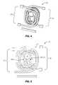
- FIGS. 1 and 2illustrate an embodiment of a galvanic isolator.
- FIG. 3is a top plan view of an embodiment of a coil configuration of the isolator of FIG. 1 .
- FIG. 4is a perspective view of another embodiment of a coil configuration of the isolator of FIG. 1 .
- FIG. 5is a plan view of the coil configuration of FIG. 4 .
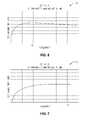
- FIG. 6is a plot of the S 21 characteristics of the coil configuration of FIG. 4 .
- FIG. 7is a plot of the S 21 characteristics of the coil configuration of FIG. 3 .
- FIG. 8illustrates a block diagram of an embodiment of a galvanic isolator comprising power and data transformers.
- FIG. 9 and FIG. 10illustrate an embodiment of a galvanic isolator package.
- FIG. 11illustrates another embodiment of a galvanic isolator package.
- FIG. 12illustrates still another embodiment of a galvanic isolator package.
- FIG. 13is schematic illustration describing an embodiment of the transfer of data via a galvanic isolator.
- FIG. 14is a diagram illustrating an embodiment of the data signals that are input to the galvanic isolator of FIG. 1 .
- FIG. 15is a timing diagram illustrating an embodiment of the signals output by the positive and negative pulse generators of FIG. 13 .
- FIG. 16is a schematic diagram of an embodiment of the edge detector of FIG. 13 .
- FIG. 17shows schematic diagrams of circuits used for the pulse generators of FIG. 13 .
- FIG. 18is a schematic diagram of an embodiment of a driver located between the circuit of FIG. 17 and the transmitter coil.
- FIG. 19shows an embodiment of a common mode rejection circuit.
- FIG. 20Ais a detailed diagram of an embodiment of a two-stage common mode amplifier.
- FIG. 20Bshows a circuit configured to separate voltage levels between a gate drive for a PMOS output device and an NMOS output device.
- FIG. 21shows a sequence of pulses as they are transmitted and received by various portions the circuitry disposed in one embodiment of galvanic isolator 20 .
- FIG. 22is a block diagram of an embodiment of the receiver circuit 22 of FIG. 2 .
- FIG. 23is a schematic diagram of an embodiment of the preamplifier of FIG. 22 .
- FIG. 24is a schematic diagram of an embodiment of the amplifier of FIG. 23 .
- FIG. 25is a schematic diagram of an embodiment of the comparator of FIG. 22 .
- FIG. 26is a schematic illustration of an embodiment of a delay element of FIG. 25 .
- FIG. 27is a schematic illustration of an embodiment of the decoder of FIG. 22 .
- horizontalas used herein is defined as a plane substantially parallel to the conventional plane or surface of the substrate of the invention, regardless of its actual orientation in space.
- verticalrefers to a direction substantially perpendicular to the horizontal as defined above. Terms such as “on,”, “above,” “below,” “bottom,” “top,” “side,” “sidewall,” “higher,” “lower,” “upper,” “over” and “under” are defined in respect of the horizontal plane discussed above.
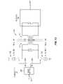
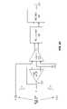
- substrate 33 and coil transducer 39 , coils 23 and 24form a high voltage isolation data signal transfer or power transformer device, which is referred to herein as a galvanic isolator 20 .
- the coil 23is sometimes referred to as a first coil or a transmitter coil and the coil 24 is sometimes referred to as a second coil or a receiver coil. As shown in FIG.
- the transmitter coil 23is separated from the receiver coil 24 by at least portions of substrate 33 , and transmitter coil 23 and receiver coil 24 are spatially arranged and configured respecting one another such that at least one of power and data signals may be transmitted by transmitter coil 23 to receiver coil 24 across a gap or dielectric barrier comprising electrically insulating, non-metallic, non-semiconductor, low dielectric loss material disposed therebetween, and from which at least portions of substrate 33 are formed.
- a dielectric barriercomprises coil transducer 39 , which includes substrate 33 and electrically insulating layers 34 and 37 disposed atop and below substrate 33 .
- Input or transmitter circuit 21is operably connected to first transmitting coil 23 and output or receiver circuit 22 is operably connected to second receiving coil 24 .
- Coil transducer 39 and substrate 33 disposed therewithinmay comprise any of a number of different non-metallic, non-semiconductor, low dielectric loss materials, more about which is said below.
- coil transducer 39 and substrate 33are capable of withstanding several kilovolts of potential difference between the input and output sides of isolator 20 , and thus exhibit high voltage breakdown performance characteristics.
- Transmitter circuit 21changes an incoming signal waveform into a signal having a waveform suitable for driving primary transmitting coil 23 .
- Receiver circuit 22is configured to change the signal exiting secondary receiver coil 24 back into a waveform that looks like the incoming signal.
- Transmitter circuit 21 , receiver circuit 22 , and coil transducer 39are preferably packaged in a format compatible with standard electronics assembly processes, such as printed circuit board assembly techniques.
- packagingcomprises mounting the various components of galvanic isolator 20 on a lead frame, wirebonding the components together, and surrounding them with a molding material to hold everything together after sacrificial metal leads have been separated from the lead frame and formed into standard integrated circuit leads.
- design of the leadframeis important to avoid degrading the performance of galvanic isolator 20 .
- galvanic isolator 20comprises transmitter circuit 21 and receiver circuit 22 , which in one embodiment comprise coils 23 and 24 disposed on opposing top and bottom sides of substrate 33 . In another embodiment, coils 23 and 24 are disposed on the same side of substrate 33 .
- circuits 21 and 22are connected to bond pads 37 , 38 and 47 on the top surface of layer 34 .
- transmitter circuit 21 and receiver circuit 22may be attached to a lead frame and connected by wire bonds to bond pads attached to coils 23 and 24 .
- Other packaging embodimentsare also contemplated.
- coils 23 and 24are fabricated by lithographically patterning metal layers on the surface of substrate 33 , although many other means of forming coils 23 and 24 are contemplated, such as placing such coils on different layers or substrates and then laminating the substrates or layers together.
- an electrically insulating, non-metallic, non-semiconductor, low dielectric loss layer or substratemay be disposed below coils 23 and 24 .
- transmitter circuit 21 and receiver circuit 22are integrated circuits or chips.
- Substrate 33 and/or coil transducer 39are formed of an appropriate electrically insulating, non-metallic, non-semiconductor, low dielectric loss materials.
- a suitable such materialhas a dielectric loss tangent at room temperature that is less than about 0.05, less than about 0.01, less than about 0.001 or less than about 0.0001.
- the material employed to form substrate 33 of the inventionis a non-semiconductor material, we define dielectric loss tangent values associated therewith herein to permit comparison of the novel substrate material of the invention to known semiconductor materials.
- suitable materials for forming substrate 33 and/or coil transducer 39also include, but are not limited to, one or more of printed circuit board material, FR4 and other printed circuit board materials, fiberglass, glass, ceramic, polyimide, polyimide film, a polymer, an organic material, a combination of an organic filler such as epoxy and an inorganic solid such as glass, a flex circuit material, epoxy, epoxy resin, a printed circuit board material, plastic, DUPONTTM KAPTONTM, DUPONTTM PYRALUX ABTM laminate, and a ROGERSTM material (e.g., PTFE—or polytetrafluoroethylene—and glass, PTFE and ceramic, PTFE, glass and ceramic, or thermoset plastic).
- a ROGERSTM materiale.g., PTFE—or polytetrafluoroethylene—and glass, PTFE and ceramic, PTFE, glass and ceramic, or thermoset plastic.
- substrate 33is formed from material from which substrate 33 is formed.
- material from which substrate 33 is formedwill, in general, depend on cost, the degree or amount of electrical isolation or voltage breakdown protection that is desired, the particular application at hand, and other factors or considerations.
- glass and ceramic substratesare well suited for applications involving high voltages; to reduce manufacturing and processing costs, flex circuit substrates may be employed.
- substrate 33has sufficient thickness between the upper and lower horizontal surfaces thereof, and electrical insulation characteristics appropriate, to withstand the relatively high breakdown voltages for which galvanic isolator 20 and coil transducer 39 may be designed.
- a breakdown voltage between transmitter coil 23 and receiver coil 24exceeds about 2,000 volts RMS when applied over a time period of about one minute. In other embodiments, the breakdown voltage between transmitter coil 23 and receiver coil 24 exceeds about 2,000 volts RMS when applied over six minutes or over 24 hours.
- even higher breakdown voltagescan be withstood by coil transducer 39 , substrate 33 and galvanic isolator 20 , such as about 2,500 volts RMS, about 3,000 volts RMS, about 4,000 volts RMS and about 5,000 volts RMS for periods of time of about 1 minute, 6 minutes and/or 24 hours.
- substrate 33 and/or coil transducer 39has a thickness between the upper and lower horizontal surfaces thereof ranging between about 0.5 mils and about 10 mils, or between about 0.5 mils and about 25 mils. In one embodiment, the thickness of substrate 33 and/or coil transducer 39 exceeds about 1.5 mils. In another embodiment, substrate 33 and/or coil transducer 39 comprises a plurality of layers, where at least one of the layers comprises a low dielectric loss material. As will be seen by referring to the Figures hereof, coil transducer 39 is generally thicker than substrate 33 . For example, in one embodiment, coil transducer 39 is 19 mils thick, while substrate 33 disposed therein is 10 mils thick.
- each of coils 23 and 24has an outer end and an inner end. Each of these ends is connected to an appropriate terminal on the transmitter or receiver circuit associated therewith.
- a first electrical connectionis established using a first trace formed with a first coil when the metal layer from which the first coil is patterned is etched, and a second electrical connection is established with the first coil using a patterned metal layer on an outer surface of coil transducer 39 .
- an electrical connection to inner end 26 of transmitter coil 23is established through trace 25 disposed on the top surface of electrically insulating layer 34 and through vertical via 35 to underlying conductor 26 (from which transmitter coil 23 is formed).
- an electrical connection to an outer end of transmitter coil 23is established through trace 27 disposed within electrically insulating layer 34 and through vertical via 36 to overlying bond pad 47 .
- An electrical connection to an outer end of transmitter coil 23is made through trace 27 , which may be patterned from the same layer as transmitter coil 23 .
- Trace 27is connected electrically to circuit 22 by via 36 disposed through layer 34 .
- Circuit 21is electrically connected to the outer end of receiver coil 24 by trace 29 and via 30 .
- Trace 29may be patterned from the same metal layer as receiver coil 24 .
- An inner end of receiver coil 24is electrically connected to circuit 21 by trace 28 disposed on the bottom surface of electrically insulating layer 37 through via 31 .
- Insulating layersmay be added atop or below the layers of metal, and may encapsulate or have disposed therewithin traces 25 and 28 so as to prevent electrical contact from being established between traces 25 and 28 and any external electrical conductors or surfaces that might otherwise come into contact with traces 25 and 28 .
- FIGS. 1 and 2may be simplified to form two different metal layers disposed on a single substrate 33 .
- coil transducer 39may be constructed from two metal layers that are deposited and patterned on opposing sides of substrate 33 .
- the top metal layermay be patterned to provide transmitter coil 23 and the various connection pads utilized by transmitter circuit 21 and receiver circuit 22 on a top surface of substrate 33 .
- the bottom metal layermay be used to fabricate receiver coil 24 , which underlies transmitter coil 23 and forms second coil of the transformer on a bottom surface of substrate 33 .
- the bottom layermay also be patterned to provide traces that are used to connect receiver coil 24 to wire bond pads disposed on the top surface of substrate 33 through vertical vias.
- Transmitter coil 23may then be connected to transmitter circuit 21 by wire bonds, and receiver coil 24 may be connected to receiver circuit 22 by a trace patterned from the top metal layer and by a wire bond.
- wire bond padsare electroplated.
- the various connection pads for connecting coil transducer 39 to external circuits that are to be isolated by coil transducer 39may also be patterned from the top metal layer.
- the structures illustrated in FIGS. 1 and 2may be fabricated using a conventional printed circuit board fabrication line.
- the cost of manufacturing coil transducer 39may be much less than that of a coil transducer constructed from silicon on a semiconductor fabrication line.
- silicon substratesare known electrical conductors or semi-conductors, and do not exhibit the low dielectric loss properties of the substrates and coil transducers of the invention.
- Embodiments of coil transducer 39 based on flexible organic/inorganic or organic substratesare particularly attractive.
- Printed circuit boards or circuit carriersare known in the art, and hence need not be discussed in detail here.
- substrates 33 and coil transducers 39 of the inventionthat are formed from printed circuit board materials do provide an excellent low-cost alternative to silicon-based materials.
- Printed circuit board materialsare less expensive, easier to handle, and more amenable to quick design or manufacturing changes than silicon-based materials.
- printed circuit boardsmay be fabricated by depositing a thin metal layer, or attaching a thin metal layer, on a somewhat flexible organic/inorganic substrate formed of fiberglass impregnated with epoxy resin and then converting the layer into a plurality of individual conductors using conventional photolithographic techniques. Additional metal layers may be added atop the thin metal layer after an intervening electrically insulating layer or coating has been laid down on the thin metal layer.
- Flex circuit technologymay also be employed to form substrate 33 and/or coil transducer 39 of galvanic isolator 20 , where substrate 33 and/or coil transducer 39 are made of an organic material such as polyimide. Films and laminates of this type are available commercially from DUPONTTM and utilize substrate materials known as KAPTONTM made from polyimide. In some cases, a plurality of polyimide layers may be laminated with an adhesive to form substrate 33 and/or coil transducer 39 .
- This type of circuit carrier or printed circuit boardis significantly less expensive than conventional silicon semiconductor material based approaches and can be employed to provide substrate 33 and/or coil transducer 39 having a high breakdown voltage and other desirable high voltage isolation characteristics.
- Thinner substrates 33 and/or coil transducers 39are preferred in applications where signal losses between primary and secondary coils 23 and 24 must be minimized.
- a PYRALUX APTM laminate manufactured by DUPONTTMis employed to form a 2 mil thick KAPTONTM substrate 33 , and electrically conductive copper layers and traces are added to the top and bottom surfaces thereof.
- coils 23 and 24may assume any of a number of different structural configurations and nevertheless fall within the scope of the invention.
- coils 23 and 24may assume the circular or oval spirally-wound shapes illustrated in FIGS. 1 and 2 , or may assume myriad other shapes such as rectangularly, squarely, triangularly, pentagonally, hexagonally, heptagonally or octagonally-wound shapes arranged in a horizontal plane, conductors arranged to interleave with one another within a horizontal plane, one or more serpentine conductors arranged in a horizontal plane, and so on. Any suitable structural configuration of coils 23 and 24 is permitted so long as the magnetic fields projected by one coil may be received and sufficiently well detected by the other opposing coil.
- a first coil configuration 50is shown in FIG. 3 .
- the coil configuration 50includes both the transmitter coil 23 and the receiver coil 24 .
- the coil configuration 50is representative of the transmitter coil 23 being on two layers and the receiver coil 24 being on another two layers.
- the coil configuration 50is referred to as an oval configuration and may occupy several different layers in a substrate.
- a first layer or first metalhas 13 ⁇ 8 turns.
- a second layerhas 7 ⁇ 8 of a turn.
- the traces in the first metal and the second metalare connected by a first via wherein a first via pad 51 associated with the first via is shown in FIG. 3 .
- a second via pad associated with the first viamay be located opposite the first via pad 51 .
- a second viamay connect metal three and metal four.
- a third via pad 57is associated with the second via.
- the transmitter coil 23may occupy two layers or metals.
- the receiver coil 24may have the same configuration as the transmitter coil 23 and may occupy metal 3 and metal 4 . The separation between the coils 23 , 24 described above would then occur between metal 2 and metal 3 .
- the via pad diameter, Pis approximately 150 um and the width, T, of the traces is approximately 35 um.
- the coil configurationhas an opening in the center wherein the horizontal direction (as viewed from FIG. 3 ) has a length, OPX of approximately 70 um and the orthogonal direction has a length, OPY, of approximately 35 um.
- the length OPY as shown in FIG. 3is the length when viewed substantially perpendicular to the galvanic isolator 20 . However, the length OPY may extend between different layers, so the actual length may be longer than 35 um.
- the length OPX/2is the distance between two segments.
- the first segmentis a mutual tangent segment extending between the circumference of via pad 51 and the circumference of via pad 57 , chosen so that both via pad 51 and via pad 57 lie on the same side of the segment.
- the second segmentis the inner edge of the nearest trace as shown.
- the length OPXis twice this distance. The bandwidth characteristics of this coil configuration 50 are described in greater detail below.
- the distance OPX/2is the shortest distance between the segments.
- the second of the segmentsextends along at least a portion of a substantially straight trace, wherein the substantially straight trace is located most proximate the first segment relative to other traces.
- the second coil configuration 52is shown in FIG. 4 and FIG. 5 , wherein FIG. 4 is a perspective view and FIG. 5 is a plan view.
- the coil configuration 52has the same dimensions as the coil configuration 50 , except the coil configuration 52 has 23 ⁇ 8 turns on the top layer.
- the numbers of turns in the other metal layershave increased as well. As shown below, the number of coils offers different bandwidth characteristics for the isolator 20 , FIG. 2 .
- a first plot 53shows the S 21 characteristics of the first coil configuration 50 .
- the peak transmissionoccurs at a frequency f 2 .
- This peakis quite broad so the coil transmission has a wide bandwidth.
- a second plot 54shows the S 21 characteristics of the coil configuration 52 .
- the peak frequencyis lower at f 1 , and the peak has a higher magnitude.
- the peakis still broad, but the bandwidth is narrower than the plot 53 .
- the addition of turns in the coilincreases the magnitude of the transmission throughput while reducing the peak frequency and bandwidth. Adding more turns may be disadvantageous to coil design.
- the coil configuration 52is used in the galvanic isolator 20 .
- galvanic isolator 20may comprise transformers in which the electronic and electrical components on one side of substrate or isolation barrier 33 are powered by a power source disposed on the opposing side of substrate 33 .
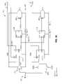
- FIG. 8there is shown galvanic isolator 20 comprising power section 150 and data transfer section 160 .
- Data transfer section 160includes an isolation gap that blocks transients and/or performs voltage shifts between the circuitry disposed on the transmitter side of the isolation gap and the circuitry disposed on the receiver side of the isolation gap.
- Galvanic isolator 20utilizes two transformers.
- Transformer 162provides an isolation barrier for the transfer of data between transmitter 21 and receiver 22 .
- Transformer 153is used to transfer power from power supply 151 disposed on the transmitter side of the isolation gap to power supply 155 disposed on the receiver side of the isolation gap.
- Power section 150includes optional power supply 151 configured to power circuitry on both sides of the isolation gap.
- Inverter 152generates an AC or oscillatory power signal from the DC power provided by power supply 151 .
- the AC or oscillatory power signalis transferred to the receiver side of the isolation gap by a power transformer 153 .
- the output of the secondary winding of power transformer 153is rectified by converter 154 to provide isolated power supply 155 that is used to power receiver 22 .
- the DC potentials provided by power supplies 151 and 155may be the same or different, depending on the particular galvanic isolator design and application at hand.
- Power transformer 153can provide a voltage step up or step down to facilitate the generation of the different output voltages.
- powermay also be derived from a train of pulses applied to power transformer 153 from a source external to galvanic isolator 20 .
- galvanic isolator 20coil transducer 39 , and substrate 33 may be configured as high voltage isolation data transfer devices, power transformers, or both.
- transformeror “transducer” as employed herein means a device capable of transmitting and receiving power or data signals, or power and data signals, across a gap or dielectric barrier formed of an electrically insulating material.
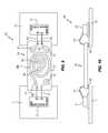
- FIGS. 9 and 10there are shown top and side views of one embodiment of galvanic isolator 20 , respectively, where input lead frame 71 and output lead frame 73 underlie and extend beneath portions of substrate 33 and coil transducer 39 .
- Input lead frame 71 and output lead frame 73are preferably connected to coil transducer 39 such that electrically conductive portions of input lead frame 71 and output lead frame 73 do not extend beneath substrate 33 and coil transducer 39 to locations disposed vertically directly beneath transmitter coil 23 or receiver coil 24 .
- input lead frame 71 and output lead frame 73are connected to coil transducer 39 such that input lead frame 71 and output lead frame 73 are mechanically connected to a lower side of coil transducer 39 .
- input lead frame 71 and output lead frame 73are mechanically connected to opposing top and bottom sides, respectively, of coil transducer 39 , such as is shown in FIG. 11 .
- Transmitter circuit or integrated circuit 21may then be mounted on the input side of leadframe 71 next to the input side of coil transducer 39
- receiver circuit or integrated circuit 22may then be mounted on the output side of leadframe 73 next to the output side of coil transducer 39 .
- the electrical potential difference between lead frames 71 and 73 and coil transducer 39may be several kV; in some embodiments lead frames 71 and 73 may be held at or near electrical ground.
- Mounting of integrated circuits 21 and 22 on lead frames 71 and 73can be accomplished with epoxy 68 and 69 .
- Epoxy 68 and 69are preferably electrically non-conductive to reduce the possibility of unwanted short circuits being created through the epoxy.
- Transmitter circuit 21is preferably wirebonded to the input side of coil transducer 39 though wirebonds 41 and 48 .
- Receiver circuit 22is preferably wirebonded to the output side of coil transducer 39 through wirebonds 42 and 43 .
- substrate 33 and/or coil transducer 39are preferably fabricated to have a thickness between their respective upper and lower surfaces sufficient to prevent high voltage arcing.
- One advantage of the materials employed to form substrate 33 and/or coil transducer 39 of the inventionis that substrate 33 and/or coil transducer 39 may be substantially thicker than is generally possible or financially feasible in commercial applications which employ conventional semiconductor materials and manufacturing processes.
- substrate 33 and/or coil transducer 39may have thicknesses ranging between about 1 mil and about 25 mils, between about 1.5 mils and about 25 mils, or between about 2 mils and about 25 mils.
- DTIdistance-through-insulation
- substrate 33 and/or coil transducer 39 of the inventionmay be formed using any of a number of different manufacturing processes and electrically insulating, non-metallic, non-semiconductor, low dielectric loss materials described above. These processes and materials are amenable to processing electrically insulating materials in bulk and do not require the expensive and elaborate procedures required to handle semiconductor materials such as silicon. Moreover, substrate 33 and coil transducer 39 of the invention provide superior high voltage breakdown performance characteristics respecting silicon-based devices owing to their increased distances-through-insulation (more about which is said above).
- substrate 33 and coil transducer 39 of the inventionexhibit substantially increased distances-though-insulation and thicknesses respecting prior art galvanic isolators having silicon substrates (which were generally limited to thicknesses of less than 1 mil), substrate 33 may be configured to impart substantial mechanical rigidity and strength to coil transducer 39 and galvanic isolator 20 .
- substrate 33 and coil transducer 39 of the inventionare mechanically robust and strong, may be mounted directly on lead frames, and may be handled without special care.
- both sides of substrate 33 and/or coil transducer 39may easily have coils or other components formed or mounted thereon owing to the radically different nature of the manufacturing processes used, and the materials employed, to form substrate 33 and/or coil transducer 39 .
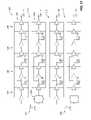
- channelsmay be accommodated in a single package by stacking channels side by side along the long dimension of a package such as an SO-16 widebody so that all channels share the same input lead frame and ground, and so that all channels share the same output lead frame and ground.
- a packagesuch as an SO-16 widebody
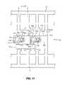
- FIG. 11there is shown a flip lead frame arrangement for dual galvanic isolator 20 .
- Each of integrated circuits 21 and 22contains two channels. This design provides two channels rather than the single channel configuration illustrated in FIGS. 4 and 5 .
- Lead frames 71 and 73are designed to permit a flip, as is the case in many opto-isolator lead frames finding common use today.
- integrated circuit 22 a,b and the nearby ends of coil transducers 39 a and 39 bare attached to corresponding respective portions of lead frame 73 and wirebonded thereto.
- Integrated circuit 21 a,bis attached to lead frame 71 .
- lead frame 73is flipped over into the position shown in FIG.
- coil transducer 39 a and 39 bare attached to corresponding sides of lead frame 71 , and finally wirebonded together.
- dual-channel devicesmay be configured to have separate transmitter circuit chips 21 and receiver circuit chips 22 for each channel.
- FIG. 12shows another embodiment of a package of the invention, also configured for two channels.
- the embodiment illustrated in FIG. 12is a small format package design that includes two coil transducers 39 a and 39 b , a dual-channel transmitter IC 21 a,b , and a dual-channel receiver IC 22 a,b.
- isolator 20 based on such substrate 33 and/or coil transducer 39may not exhibit good high voltage breakdown performance characteristics unless all potential arcing paths within isolator 20 have been eliminated or blocked.
- a thick coverlayis preferably employed in a package. No voids should be present between the layers of galvanic isolator 20 and/or coil transducer 39 , or between the various components of isolator 20 and the coverlay. The adhesion between the different layers of coil transducer 39 should remain strong during die separation, so that no delamination results. It is good practice to locate the bus bars for electroplating together near the appropriate wirebond pads in order to avoid busbar-to-busbar conduction along the sides of coil transducer 39 .
- the space between the LED and the receiver containing a photodetectoris typically filled with an optically transparent insulating material such as silicone.
- an optically transparent insulating materialsuch as silicone.
- siliconemay still be employed advantageously. Silicone is a considerably better electrical insulator than air and also adheres well to many other materials, and therefore may be used advantageously to inhibit the formation of air gaps between different parts of galvanic isolator 20 and/or coil transducer 39 during thermal cycling. Furthermore, silicone has low dielectric loss characteristics and thus does not disturb the operation of coils 23 and 24 .
- siliconeis therefore emplaced around at least portions of coil transducer 39 and/or galvanic isolator 20 to enhance the electrical isolation characteristics of isolator 20 . While this step may be omitted to reduce costs, performance may also be compromised if silicone is not used.
- Galvanic isolator 20 and/or coil transducer 39are preferably overmolded.
- lead frame 71 , coil transducer 39 , and lead frame 73are attached to one another, wirebonded, and placed in a mold.
- a melted appropriate electrically insulating molding materialsuch as epoxy is forced into the mold to encapsulate at least portions of the package.
- the molding materialis then allowed to cool and harden, thereby imparting substantial additional structural rigidity to the resulting package.
- the molding materialpreferably has an appropriate dielectric constant and low dielectric loss such that the electrical performance of galvanic isolator 20 is not degraded.
- the leadsare then trimmed and bent.
- galvanic isolators 20configured for isolated signal transfer disclosed herein are AC or oscillatory signal devices, which generally behave like differentiators in the manner in which they respond to transitions in incoming signals.
- the datais in the form of signals that are transformed as summarily described in the block diagram of FIG. 13 .
- a series of pulsesis transmitted via the galvanic isolator 20 rather than impulse-type signals.
- the pulseshave a lower frequency spectrum than impulse-type signals, which enables better transmission via the galvanic isolator 20 .
- the signals or dataare input to an edge detector 200 via an input 202 .
- the edge detector 200has a positive output 204 and a negative output 206 .
- the positive output 204is activated when the input signal transitions from a logic zero to a logic one. This transition is also referred to as a leading edge.
- the negative output 206is activated when the input signal transitions from a logic one to a logic zero. This transition is also referred to a trailing edge.
- the edge detector 200is described as having two components, a positive edge detector and a negative edge detector. It is noted that the leading edge and trailing edge described herein are for exemplary purposes. In some embodiments, a leading edge may be transition from a logic one to a logic zero and a trailing edge may be a transition from a logic zero to a logic one.
- the positive output 204is connected to a positive pulse generator 210 .
- the negative output 206is connected to a negative pulse generator 212 .
- the activation of the positive output 204activates the positive pulse generator 210 .
- activation of the negative output 206activates the negative pulse generator 212 .
- the positive pulse generator 210generates a plurality of positive pulses when activated. More specifically, the positive pulse generator 210 generates a plurality of positive pulses when the leading edge of the data signal at the input 202 is detected.
- the negative pulse generator 212generates a plurality of negative pulses when activated.
- the negative pulse generator 212generates a plurality of negative pulses when a trailing edge of the data signal at the input 202 is detected.
- the pulse generators 210 , 212may be active for a time corresponding to less than half the width of the pulse.
- the pulses generated by the positive pulse generator 210 and the negative pulse generator 212are used to drive the transmitter coil 23 .
- a drivermay be located between the pulse generators 210 , 212 and the transmitter coil 23 .
- the pulsesconsist of spectral frequencies that match the coils 23 , 24 , which provides for greater energy transfer to the coils 23 , 24 . For example, less energy is reflected from the transmitter coil 23 because of the match.
- the coilsare driven with signals, such as impulse or step functions that have high frequency components. These high frequency components do not transfer well into coils used in galvanic isolators.
- the pulses generated by the positive pulse generator 210 and the negative pulse generator 212have lower frequency components that match the transmitter coil 23 . Therefore, more energy is able to be transferred to the transmitter coil 23 and ultimately to the receiver coil 24 .
- the receiver 22receives data from the receiver coil 24 , which is the inverted signal of the signal driving the receiver coil 24 . Therefore, the receiver 22 receives a plurality of negative pulses indicating the detection of a leading edge by the edge detector 200 . The receiver receives a plurality of positive pulses indicating the detection of a trailing edge by the edge detector 200 . The receiver 22 reconstructs the original data signal received at the input 202 based on the signals received from the receiver coil 24 .
- FIG. 14Examples of the data signals that may be input to the input 202 of the edge detector 200 are shown in FIG. 14 .
- a data signal 216is received at the input 202 .
- the data signal 216 of FIG. 14is a single binary pulse and is used for exemplary purposes. It is understood that the signal received at the input 202 may be a stream of data.
- the data signal 216has a leading edge 218 and a trailing edge 220 .
- the width of the data signalis the time between the leading edge 218 and the trailing edge 220 . In the embodiment described herein, the data signal 216 has a width of ten nanoseconds.
- Illustration 224shows pulses that are generated based on the detection of the data signal 216 by the edge detector 200 .
- the edge detector 200detects the leading edge 218 and activates the positive output 204 for 3.5 nanoseconds. The activation is shown by the pulse 226 . After 3.5 nanoseconds, the positive output 204 is deactivated.
- the edge detector 200detects the trailing edge 220 , the negative output 206 generates a pulse 228 .
- the pulse 228shows the activation of the negative output 206 for a period of 3.5 nanoseconds.
- FIG. 15An embodiment of the outputs of the positive pulse generator 210 and the negative pulse generator 212 are shown in FIG. 15 .
- the positive pulse generator 210 and the negative pulse generator 212each generate three pulses during the 3.5 nanosecond duration of the pulse described above.
- the positive pulse generator 210generates three pulses that are each 2.5 nanoseconds long that overlap each other. A first pulse having a pulse width of 2.5 nanoseconds is generated, yielding the signal 230 in FIG. 15 . After a period of 0.5 nanoseconds, a second pulse having a pulse width of 2.5 nanoseconds is generated yielding the signal 232 .
- the pulses having different amplitudesfor illustration purposes. However, their amplitudes may be equal.
- a third pulse having a pulse width of 2.5 nanosecondsis generated yielding the signal 234 .
- the signal driving the coil 23consists of three overlapping pulses. It is to be understood that the use of three overlapping pulses is for exemplary purposes only and that there may be more or less than three overlapping pulses.
- the current driving the transmitter coil 23is consistent at 9 mA. It is noted that other values of the current may be used.
- the first pulse 230has an amplitude of 9 mA.
- the two pulses of 232have amplitudes of 4.5 ma each for a combined current of 9 mA.
- the three pulses of 234have amplitudes of 3 ma each for a combined current of 9 mA.
- the transmitter coil 23induces a current into the receiver coil 24 , which is detected by the receiver 22 as described in greater detail below.
- the receiver 22then recreates the data signal received at the input 202 .
- the receiver 22may detect the three pulses indicative of the leading edge 218 of a data signal 216 .
- the receiver 22may then output a logic one.
- the receiver 22may output a logic zero.
- the output of the receiver 22is the same as the data signal at the input 202 .
- the current passing through the transmitter coil 23may remain at 3 mA because the inductive properties of the coil will serve to maintain the current constant given the short pulses that are input to the transmitter coil 23 .
- FIG. 16An embodiment of a circuit 250 constituting the components in the edge detector 200 is shown in FIG. 16 .
- the input 202branches to an inverter 252 and a delay circuit 254 .
- the circuit connected to the output of the inverter 252detects the leading edge 218 of the data signal 216 and generates the positive output 204 .
- the circuit connected to the output of the delay circuit 254detects the trailing edge 216 of the data signal 216 and outputs the negative output 206 .
- the delay circuit 254causes a signal delay equivalent to the inverter 252 , which balances the timing between the upper and lower circuits. It is noted that the upper circuit and lower circuit may be referred to as individual edge detectors.
- a leading edge or positive transition received at the input 202causes a negative transition to be output by the inverter 252 .
- the output of the inverter 252is connected to the clock input of a flip flop 256 .
- the flip flop 256may be an edge triggered D flip flop. When the flip flop 256 triggers, the output Q transitions to a high or logic one level until the flip flop 256 is reset.
- the inverted output QB of the flip flop 256is connected to a delay element 258 .
- the delay element 258is triggered by the negative going transition of the inverted output QB.
- the output Q of the delay element 258transitions in a time that is based on an input Idly.
- This delaymay be 2.5 nanoseconds, which correspond to the duration of the pulses generated by the pulse generators.
- a resetis transmitted to the flip flop 256 via a NAND gate 260 .
- An input of the NAND gate 260is coupled to a master reset.
- the flip flop 256is reset, the positive output 204 returns to a logic zero state, which deactivates the positive pulse generator 210 , FIG. 13 .
- the lower circuitfunctions in the same manner as the upper circuit, but due to the lack of the inverter 252 , the lower circuit triggers on a trailing edge being received at the input 202 .
- the pulse generators 210 , 212will now be described.
- An embodiment of circuits 270 , 272 that may be used by the pulse generators 210 , 212is shown in FIG. 17 .
- the circuit 270generates the positive pulses and the circuit 272 generates the negative pulses.
- the circuit 270will be described in detail. It is noted that the circuit 272 functions in a very similar manner as the circuit 270 .
- the pulse generator circuit 270consists of a plurality of delay elements, which in the embodiment of FIG. 17 are inverters connected in series.
- the output 204 from the edge detector 200is connected to an input 276 of the circuit 270 .
- the output 206 from the edge detector 200is connected to an input 278 on the circuit 272 .
- the input 276is split to two sections. The first section is referred to as the feed 280 and the second section is referred to as the return 282 .
- the feed 280drives the transmitter coil 23 and the return provides the return path.
- the feed 280 and the return 282each have four delay stages, which are referred to individually as the first delay 284 , the second delay 286 , the third delay 288 , and the fourth delay 290 .
- Each delayhas a terminal or output that is connected to a driver that drives the transmitter coil 23 .
- each output pairis connected to a driver for the transmitter coil 23 .
- the output P1 and N1serve to provide a current path to drive the transmitter coil 23 as described below.
- three delaysare created in the circuit 270 as the second and third delays occur simultaneously.
- the circuit 270may have three delays wherein none of the delays operate simultaneously. The use of three delays is for exemplary purpose. Other embodiments may have more or less than three delays.
- the feed 280is the same as the return 282 except for an additional inverter in the feed 280 .
- the returnhas a delay element 284 that has approximately the same delay as an inverter.
- the delay element 284serves to make corresponding outputs trigger at the same time, but with opposite logic levels. For example, when the state of the input 276 changes, the state of out P1 and out N1 will change at the same time, however, they will have opposite logic levels. The same applies to all the outputs. Thus, an output out Px provides a drive and the output out Nx provides the return path.
- the transmitter coilmay have a significant current draw. Therefore, a driver may be located between the pulse generators 210 , 212 and the transmitter coil 23 .
- An embodiment of a driver 300is shown by the schematic illustration of FIG. 18 .
- the driver 300uses current mirrors in a plurality of bridges as described below to drive the transmitter coil 23 .
- the amount of current that is able to be drawnis set by the bias current Ib.
- the transmitter coil 23is connected to each of the outputs txp and txn.
- a first lead of the transmitter coil 23is connected to each of the outputs txp and a second lead of the transmitter coil 23 is connected to each of the outputs txn. Accordingly, the outputs txp are connected together in parallel and the outputs txn are connected together in parallel.
- the bridgesdetermine the polarity of the pulse generated by the transmitter coil 23 .
- the driver 300has a plurality of bridges, which are referred to individually as the first bridge 302 , the second bridge 304 , the third bridge 306 , and the fourth bridge 308 . It is noted that the outputs of the circuits 270 , 272 , FIG. 17 , are inputs to gates in the driver 300 . Reference is made to the first bridge 302 , which is similar to the remaining bridges.
- the output P1transitions to a logic 1 and the output N1 transitions to a logic zero.
- the outputs P1, N1cause gate 310 and gate 312 to turn on, which enables them to conduct current. Gates 314 and 316 are off and do not conduct current.
- the first bridge 302Based on the state of the gates in the first bridge 302 , current passes from the txp lead on the transmitter coil 23 to the txn lead.
- the first bridge 302supplies a predetermined current to the transmitter coil 23 , which may be approximately 3 mA.
- the remaining bridges in the driver 300turn on and supply current to the transmitter coil 23 .
- the second bridge 304 and the third bridge 306supply half the current of the first bridge 302 and the fourth bridge 308 .
- Each activation of the circuit 210causes current to pass from the output txp to the transmitter coil 23 and returns to the output txn. Thus, current flow remains in the same direction through the transmitter coil 23 .
- the second bridge 304 and the third bridge 306operate simultaneously for redundancy in the circuit 300 .
- three bridgesmay be provided wherein none of them operate simultaneously.
- the edge detector 200detects a trailing edge
- the same processes described aboveapply, except current flows from the txn terminal, through the transmitter coil 23 and returns via the txp terminal. More specifically and referring to the first bridge, the gate 310 and the gate 312 will turn off so current cannot flow. The gate 314 and the gate 316 turn on allowing current to flow.
- the direction of current flow through the transmitter coil 23is from the txn terminal and returns via the txp terminal, which is opposite the current flow described above. Accordingly, when the edge detector 200 detects a leading edge, current flows in a first direction through the transmitter coil 23 .
- the edge detector 200When the edge detector 200 detects a trailing edge, current flows in a second direction, opposite the first direction, through the transmitter coil 23 . Based on the different current directions, the receiver 21 is able to determine whether a leading edge or a trailing edge has been transmitted via the isolator 20 .
- Isolation circuitryallows different portions of galvanic isolator 20 and/or coil transducer 39 to operate at significantly different potentials that may arise, for example, because of DC voltage differences, power line voltage differences, or ground potential differences.
- high voltage isolationis required between coils 23 and 24 of galvanic isolator 20 and coil transducer 39 , which is achieved with the use of the materials described above to form substrate 33 .
- One difficult aspect of common mode signalsis the fast transients that arise between the grounds of transmitter circuit 21 and receiver circuit 22 .
- An inherent capacitanceexists between traces disposed on either side of substrate 33 , and in particular between coils 23 and 24 . This inherent capacitance includes capacitive coupling between the primary and secondary side of galvanic isolator/transformer 20 .
- the common mode design of galvanic isolator 20is preferably configured to absorb a transient signal of such a magnitude over such a short period of time while maintaining proper signal transmission performance characteristics. Trade-offs must be made between magnetic coupling through coil transducer 39 and the spacing between transmitter coil 23 and receiver coil 24 . As a result, the common mode rejection (CMR) design for galvanic isolator 20 becomes particularly challenging.
- CMRcommon mode rejection
- Common mode current compensationmay be achieved by a common mode amplifier whose output is capable of handling the large amounts of common mode current that are generated.
- FIG. 19One embodiment of such a CMR compensation circuit is shown in FIG. 19 , where the common mode voltage of the transmitter outputs and receiver inputs is established by a resistor divider network driven by the common mode amplifier opmAB.
- amplifier opmABis configured to provide unity gain feedback by driving the center tap of the resistor divider network to a common mode reference voltage, vcm.
- vcmis preferably set within an operating supply range. Ideally, vcm should be set to the middle of the operating supply range for optimum signal swing at both the transmitter and receiver.
- the resistors RI, R 2are preferably of low impedance (e.g., 10 ohms or less) so that any voltage drop across the resistors during a common mode event does not cause the transmitter outputs and receiver inputs to exceed the operating supply range. (Note, however, that resistors having higher impedance are also contemplated, such as impedances of about 100 ohms or less, or about 250 ohms or less.) If the signal swing at either the transmitter or receiver is allowed to exceed the operating supply range, the data transmitted across the channel will be corrupted.
- the two resistorsmust be well matched so that any mismatch in their resistance does not translate into erroneous differential signals. Since the output stage of the common mode amplifier is typically designed to handle common mode currents up to a specified amount, ESD diodes may be placed at the transmitter outputs and receiver inputs to provide further protection to isolator 20 in case the common mode current is larger than the design specifications.
- FIG. 20Ashows details of one embodiment of two-stage Class AB common mode amplifier opmAB shown in FIG. 19 .
- Amplifier opmABis a common mode current compensation amplifier operably connected to both transmitter circuit 21 and receiver circuit 22 .
- opmABsinks or sources a common mode current that may easily drive the signal level to the plus or minus power supply value with a resulting loss of data signal through the isolation channel.
- the left side of the amplifier structureis a bias system that is referenced to a bias current i b .
- This bias currentis generated in another part of the isolator 20 .
- Bias voltagesare generated in the left side of FIG. 20A .
- the input to amplifier opmABis a pair of NMOS devices which drive a folded cascode structure to the right of the input pair. Such a configuration is used to achieve high gain at a high impedance level connecting to the output stage. See also, for example, pages 752-756 of Paul R. Gray and Robert G. Meyer in “Analysis and Design of Analog Integrated Circuits”, 2 nd edition, John Wiley and Sons, New York, 1984, where similar circuit topologies are discussed in more detail.
- FIG. 20Bshows a circuit configured to separate voltage levels between a gate drive for PMOS output device PM 4 , and NMOS output device NM 3 .
- the circuit illustrated in FIG. 20Bpermits large output devices to be biased at a quiescent current level that is less than their full current sourcing or current sinking capabilities (i.e., class AB operation is achieved).
- the voltage difference between pgate and ngate signalsis controlled by PM 12 and NM 13 devices. If there is a load on the output of the amplifier that requires sourcing or sinking larger amounts of current, either PM 12 or NM 13 may turn off since either the ngate value becomes higher than vn or the pgate value becomes lower than vp.
- the device that remains onkeeps the first stage cascode structure in the proper operating region and keeps the output device on that does not have a heavy current demand with at least a minimal quiescent current level.
- PM 12 and NM 13 devicesalso have special AC signal properties. Gate bias levels vn and vp are bypassed by capacitors to ground. The two devices function as additional common gate stages that further boost the gain of the first stage at the input to the second stage, i.e., the output devices.
- An additional feature of this circuit arrangementis that the basic single pole type of roll off for the first stage circuit is preserved.
- the interface devicesare unique since they provide a means of controlling the crossover characteristics for the class AB output stage, and add minimal delay and phase shift to the signals driving the output devices. As a result, the overall amplifier is easier to stabilize in respect of AC signals, and significant extra gain is provided by the amplifier circuit for the intermediate frequency region up to several megahertz.
- the common mode output of the amplifiermust be able to sink or source very heavy currents during a common mode transient event.
- the earlier description of common mode transientsemphasizes the need for a very fast response to the sharp transients, and to keep the midpoint of the signal near 1.25 volts (or at the middle of the operating range according to one embodiment of the invention).
- Amplifier performancemay also be enhanced through proper design and selection of output devices. To keep costs down, it may be preferred to fabricate the necessary devices in an integrated circuit process that is primarily digital in nature with a few additions for analog capability.
- isolator 20must have a large Gm to increase the bandwidth thereof. It has been discovered that a fast response to fast transients may be achieved by using a very short feedback path (in respect of time delay) so that all or most of the transients may be suppressed.
- the device capabilities of the output devices for conventional CMOS processesare adequate to achieve this result if the feedback element is a capacitor from the output back to the gate of the output NMOS or PMOS device. This very short feedback path provides frequency response for correction of the common mode voltage up to about 2 GHz.
- the output stageuses local feedback at output devices PM 4 and NM 3 to accomplish fast transient suppression. Drain to gate capacitors C 0 and C 1 provide such fast response paths. Capacitors C 0 and C 1 also serve to stabilize the overall frequency response of the amplifier. There is some flexibility in the choice of capacitors C 0 and C 1 so the gain bandwidth of the amplifier structure is around 2 MHz.
- Another aspect of the operational amplifier design shown in FIG. 20Bis the local feedback circuitry around output devices PM 4 and NM 3 , which provides transient control. At the same time, the overall response of the amplifier is also relatively easily stabilized because of the first stage cascode architecture.
- coding schemesmay be employed to transmit data signals through galvanic isolator 20 and coil transducer 39 .
- a sequence of two pulsesmay be employed to represent a rising transition on the user waveform and a single pulse to represent a down transition.
- the embodiment described hereinemploys some aspects of the basic physics of the design and operation of isolator 20 and coil transducer 39 to provide a coding scheme that is relatively simple and capable of operating at a high data rate.
- Input transitionsare converted to single pulses having polarities corresponding to positive-going or negative-going transitions in the input signal. Since there is only one pulse per input transition the maximum transmission frequency is limited by the size of the individual transmitted pulses, not by the extra time needed to create multiple same-polarity pulses for transmission.
- the differentiation action of the transformer in the isolation channelproduces a multiple pulse output for the sequence of input pulses. According to one embodiment of receiver circuit 22 , the sequence of pulses also may be checked to verify data integrity.
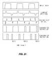
- FIG. 21One possible pulse sequence is illustrated in FIG. 21 .
- the information transfer through the isolation channeluses a sequence of pulses that is initiated by input signal transitions, converted to current pulses driving transmitter coil 23 in the transmitter, passed through coil transducer 39 and then differentiated as shown at receiver coil 24 .
- the output voltage peaksare sensed and read by receiver circuit 22 , and used to construct an output pulse sequence.
- comparator outputsare processed through a decoder that produces a positive- or negative-going edge on the rising edge of the second pulse in each sequence of pulse pairs provided to the comparator as positive and negative outputs.
- the output of coil transducer 39is shown in FIG. 21 as “Voltage Out of Coil.” Due to the nature of the coil transducer 39 , the primary input current pulses (“Input Data” in FIG. 21 ) are transformed into a sequence of pulses in the secondary output. FIG. 21 shows that “Voltage Out of Coil” signals occur in pulse pairs. A negative pulse is quickly followed by a positive pulse (or a positive pulse is followed by a negative pulse, according to the manner in which coil transducer 39 is wired and configured). In one embodiment, the second pulse in such paired pulses must occur within a short period of time after the first pulse has occurred (e.g., about 10 ns or a similar period of time) to be detected by receiver circuit 22 as a data pulse and not noise.
- an additional check on the accuracy of the pulses detected by receiver circuit 22may be performed.
- a minus ( ⁇ ) pulse followed by a plus (+) pulsemust be followed by a plus (+) pulse followed by a minus ( ⁇ ) pulse.
- a plus (+) pulsemust be followed by a minus ( ⁇ ) pulse, which must be followed by a minus ( ⁇ ) pulse followed by a plus (+) pulse.
- the novel transmitter and receiver circuits of the inventionprovide certain advantages not found in prior art galvanic isolators configured to transfer data signals across a dielectric barrier.
- One such advantageis that the signaling scheme employed in transmitter circuit 21 and receiver circuit 22 is much simpler, more robust and exhibits superior CMR performance respecting prior art signaling methods employed in such devices.
- Receiver circuit 22is able to handle excess current and distinguish real data signals from noise signals. Both such performance characteristics are required if high CMR performance is to be attained in the presence of interfering noise pulses.
- the receiver 22may be configured to monitor differential signals transmitted across the isolator 20 and produce an output that is a minimally delayed version of the input signal provided to transmitter 21 . Although the output of the receiver 22 is a delayed version of the input signal to the transmitter 21 , it should nevertheless preserve the pulse width of the input signal so that signal integrity may be maintained.
- the common mode voltage of the receiver inputsmay be set using the common mode schemes described above for transmitter common-mode signals.
- FIG. 22A block diagram of an embodiment of the receiver 22 is shown in FIG. 22 .
- the receiver 22has clamping circuit 320 (sometimes referred to as a common mode holding circuit), a fully differential preamplifier 332 , a fully differential high speed comparator 334 , and a decoder stage 336 that reconstructs the received signals.
- the receiver 22produces an accurate reproduction of the input signal provided to the galvanic isolator 20 .
- the components of the receiver 22are described in greater detail below.
- the receiver coil 24is connected to two terminals T 1 and T 2 in the receiver 22 .
- Resistors R 1 and R 2are connected in series between the terminals T 1 and T 2 .
- the clamping circuit 320includes a differential amplifier 338 and the two resistors, R 1 and R 2 .
- the resistors R 1 and R 2may each have values of about 25 ohms.
- the output of the amplifier 338 and the resistors R 1 , R 1are connected together at a node N1.
- the resistors R 1 and R 2 in combination with the amplifier 338maintain the voltage at the node N1 at a preselected voltage. For example, in a 2.5 volt system, the node N1 may be maintained at approximately 1.25 volts.
- FIG. 23An embodiment of a circuit 340 of the preamplifier 332 of FIG. 22 is shown in FIG. 23 .
- the embodiment of the circuit 340includes a high performance Cherry Hooper [Chris D. Holdenried, Michael W. Lynch, and James W. Haslett, “Modified CMOS Cherry-Hooper Amplifiers with Source follower Feedback in 0.35 um technology,” Proceedings of the 29 th European Solid-State Circuits Conference, pp. 553-556, 2003] circuit topology to provide a gain of about 6 with about 1 GHz bandwidth.
- the preamplifier 332is optimized for fast signal performance. It provides some gain to the incoming signals so that the requirement on the resolution of the follow on comparator 334 , FIG. 22 , is relatively eased.
- the high bandwidth of the circuit 340allows the narrow output pulses generated by the receiver coil 24 to pass through with minimal attenuation.
- the multiple overlapping current pulses driving the transmitter coil 23spread the transmit pulse energy over a longer period than the case if a single current pulse is used.
- the overlapping pulsesenable optimization of the bandwidth of the receiver 22 .
- the bandwidth of the preamplifier 332must be higher than the bandwidth of signals being transmitted therethrough.
- the bandwidth of the preamplifier 332 in embodiments described hereinmay be designed to be just sufficient for the system to achieve its desired data baud rate.
- the possibility of residual common mode signals from the receiver coil 24 causing difficulties in the preamplifier 332are reduced greatly by a low frequency offset correction amplifier driving a second set of inputs to the Cherry Hooper amplifier.
- the offset correction mechanismalso provides DC balanced inputs to the follow on comparator.
- the terminals T 1 and T 2 from the receiver coil 24are input to the Cherry Hooper amplifier 342 . It is noted that amplifiers other than a Cherry Hooper may be used herein.
- the terminals T 1 and T 2provide a differential input to the amplifier 342 .
- a low frequency integrator 346provides feedback for the amplifier 342 .
- the low frequency integrator 346includes a differential amplifier 348 with capacitive feedback. The output of the low frequency integrator 346 provides the above-described offset correction into the amplifier 342 .
- FIG. 24is a schematic diagram of an embodiment of the amplifier 342 of FIG. 23 .
- the amplifier 342uses an NMOS design for the Cherry Hooper gain stage.
- the N devicesare used because of better matching of the natural threshold devices and the relatively high gain, Gm, of the devices. This combination provides better high frequency common mode rejection when used with the low frequency feedback amplifier shown in FIG. 23 .
- the amplifier 342tolerates a significant common mode input range while providing a consistent output common mode level that is optimized for the follow on comparator circuit.
- FIG. 25is a schematic diagram of an embodiment of the comparator 334 of FIG. 22 .
- the comparator 334has a fully differential design with current mirror load structures having a differential output gain of about 80.
- the fully differential designprovides good common mode rejection which is important not only for noise rejection during normal operation, but also during a common mode event to ensure that common mode transients do not transform into differential signals and disrupt receiver operation.
- the current mirror output structureshave additional feedback from a follow on inverter stage to provide positive feedback for comparator operation with hysteresis.
- the threshold for the comparatoris set at about 80 mV so as to be reasonably away from the noise level.
- the hysteresis window of about 30 mVfurther improves system noise immunity.
- the fixed pulse widthsare achieved by using controlled delay elements 350 , 352 with 1.5 ns delay and a feedback line back to the first inverter stage to turn off the pulse after 1.5 ns.
- the input + and input ⁇ of the comparator 334are coupled to the outputs out + and out ⁇ of the amplifier 342 , FIG. 24 .
- a pulseis generated at the respective outputs CP and CN.
- a hysteresisis used, which in this embodiment is 30 mV.
- the output pulsetriggers the delay circuits 350 , 352 , which reset the outputs CP and CN after a preselected period. In the embodiment of FIG. 25 , the preselected period is approximately 1.5 ns. Thus, the maximum pulse width generated by the comparator 334 is 1.5 ns.
- FIG. 26is a schematic illustration of an embodiment of one of the controlled delay elements 350 , 352 of FIG. 25 .
- the delay element 350has an initial inverter stage 360 followed by a bias current controlled inverter 362 between the nodes X 1 and X 2 .
- the center two devices in the current controlled inverter 362act as a regular inverter stage with the amount of current used during the transitions controlled by the top and bottom current source devices 364 , 366 .
- a capacitor C 0is connected between VSA and node X 2 .
- the timing from node X 1 to node X 2is primarily controlled by a combination of the bias current value coming into node BB 1 and the capacitor value C 0 that is attached to node X 2 .
- the string of 4 devices in the inverter stages 370includes two center devices connected to node X 2 and the gates of the two center devices connected to node X 3 is a non-retriggering prevention circuit. Once the delay generation sequence has started these devices force the completion of the delay time before the timing of a follow on event can start. In effect, the mechanism is a filter blocking very fast repeated input pulses. Temperature, process, and supply voltage variations can cause significant variations in the delay values of inverter strings.
- the delay elementsare designed to be symmetrical in delay for a positive going input edge and a negative going input edge.
- the bias currentis used as a temperature compensation mechanism. As temperature increases the inherent delay in the delay element 350 will increase due to the TC of the devices.
- the bias current provided external to the delay element 350is designed with a positive TC so as temperature increases the delay will stay constant.
- the determination of the delay by a combination of the bias current and the capacitor C 0 on node X 2also reduces the susceptibility to process variations. Supply voltage variation is primarily reduced by operation of the delay elements along with the core of the transmitter and receiver circuits on an internally regulated supply voltage.
- This embodiment of the delay elementsis used in both the transmitter and receiver chips in the isolator 20 .
- FIG. 27is schematic illustration of an embodiment of the decoder 336 of FIG. 22 .
- the decoder 336receives inputs from the comparator and, based on these inputs, reconstructs the original data signal input to the isolator 20 .
- the decoder 336receives inputs CP and CN from the comparator 334 .
- the preamplifier 332 and the comparator 334turn the pairs of negative going pulses followed by positive going pulses or the alternative sequence into short pulses.
- the pulsesare approximately 1.5 ns long with characteristic spacing between the pairs of pulses representing either of the two sequences.
- the output CPrepresents positive pulses that have been received and the output CN represents negative pulses that have been received.
- the decoder 336needs to determine which pairs of pulses represent a valid input positive transition to the isolator 20 and which pairs represent a valid input negative transition. Invalid detections need to be discarded by the decoder 336 .
- the information to determine whether a given pulse pair is a valid representation of a transitionis contained in the timing. If two pulses are a valid pulse pair several criterion must be met. The time between the initial pulse and the follow on pulse must be less than a preselected value T 1 . A period longer than T 1 indicates that there was either a false detection of a first edge or that the second edge of the pulse was not detected. The timing requirement may be implemented fairly precisely since the same type of controlled delay structure is used in both the transmitter 21 and receiver 22 .
- Another test for a valid pulse pairdetermines whether the pulses alternate. For example, a CP should be followed by a CN and visa versa. If the pulse pairs are not received, an error has occurred. In some embodiments, the decoder 336 will observe invalid alternation sequences and ignore them until a proper pair is received.
- the embodiment of the circuit 380is divided into 4 rows of logic elements and controlled delay elements.
- the first row and second rowcheck for valid pulse pair sequences.
- the CP pulseis used to clock a first flip flop 382 which follows an inverter 384 .
- the first flip flop 382may be a D flip flop.
- the D input for flip flop 382ARM_P2
- the QB outputtriggers a controlled delay element 386 . There is no output from the controlled delay element 386 for a time duration T 1 , wherein T 1 is 6 ns.
- a negative transitionoccurs on QB which feeds back through a NAND gate 388 to reset the first flip flop 382 .
- the Q output of the first flip flop 382is in a state that will enable the D input of a second flip flop 390 . If the CN pulse from the comparator 334 occurs during the time T 1 the second flip flop 390 will also change state, i.e. the Q output will have a positive transition.
- a NAND gate 392produces a negative going pulse indicating a valid pulse pair has been received.
- the pulse generated by the NAND gate 392does not go directly to the output, but instead goes to the 4th row of the circuit 380 to determine if the pulses alternate.
- the first 3 gates of row 3 and row 4 of the circuit 380are state RS flip flops that keep track of which type of pulse pair is required next.
- the first gates 396 A (row 3) and 396 B (row 4)is active only during initial power on. The objective is to put the system into a known state at power up so the decoder 336 will operate properly for subsequent inputs.
- the third logic gate 394 in row 4is one half of an arm state flip flop, composed of gate 394 B and gate 394 A, the gate directly above it. This flip flop 394 does the set up for the alternation of pulse sequences test.
- the P1_OUT pulse generated by the row 1 circuitrychanges the state of the RS arm flip flop 394 so that ARM_N1 becomes active.
- the next pulse pair expectedis a CN pulse followed by a CP pulse.
- the ARM_N1 signalpasses through some additional circuitry in row 4 and emerges as ARM_N2 as described below. This signal is used to arm the circuitry in row 2 so the CN pulse followed by CP pulse combination is ready to be detected by row 2.
- the arm flip flop 394 A,Bchanges state, the ARM_P1 signal goes to the last inverter 396 in row 1 which generates the OUT1 signal for the decoder. In this case, the output is a positive transition.
- the row 2 circuitsoperate in an analogous manner to the row 1 circuits for the CN followed by CP pulse pair sequence.
- the arm state flip flopwill change state, causing a positive transition on the ARM_P1 signal, which in turn causes OUT1 to have a negative transition. Therefore, the positive transition followed by a negative transition on OUT1 will follow the user input which is the desired result.
- the second output OUT2is the inverse of OUT1 and is provided as an optional output.
- the D flip flops, delay elements and gates in the remaining circuitry in row 3 and row 4are inhibit circuits for the cases of repeated CP CN pulse pairs or repeated CN CP pulse pairs.
- a valid CP followed by a CNhas occurred.
- the resultis ARM_N1 is in the active state and a CN followed by a CP pulse is expected to occur next. Instead a CP pulse followed by a CN pulse occurs.
- the ARM_P1 signalis in the non active state, so the CP pulse will not do anything to the row 1 circuits.
- the second half of the sequenceis a CN pulse which might activate the circuitry in row 2. This situation has a small potential to cause confusion in the decoder 336 if the system is operating near the maximum signal speed.
- a method to eliminate ambiguityis to acknowledge that a repeat CP pulse did occur and use it to inhibit the follow on CN pulse that would occur if this is a repeat CP CN pulse pair.
- the arm signal that actually is connected to row 2is the ARM_N2 signal from the fourth row of circuitry.
- the ARM_N1 signalactivates a D flip flop which triggers a 2.5 ns delay element 398 which in combination with a NAND gate 400 produces a ARM_NQ signal for duration T 0 , 2.5 ns, which inhibits the ARM_N2 signal from going into the active state when the CN pulse in the CP CN pair would be present.
- This inhibit circuitryis in the later part of row 4. There is similar inhibit circuitry in row 3 for the case of repeated CN CP pairs.
- a DC refresh circuitis preferably included in the system to ensure correct DC levels when no transitions are present in the data signals being transmitted.
- the DC refresh circuitcomprises a watchdog timer disposed in transmitter circuit 21 that is configured to monitor input signal transitions. If no signal transition occurs after a certain predetermined or programmed timeout or period of time, the watchdog circuit will initiate internal “keep-alive” pulses to keep the channel active so that the output DC state is maintained.
- a watchdog circuitmay also be included in receiver circuit 22 to monitor signal transitions at the receiver inputs.
- the receiver watchdog circuitwill set the output to a default state.
- the “keep-alive” pulsesutilize a double edge encoding scheme. For example, the refresh for a high level is a 1 to 0, followed by a 0 to 1. The refresh for a low level is a 0 to 1, followed by a 1 to 0.
- the internal “keep-alive” pulsestravel through the same channel as the external input signal so there is no need for a separate refresh channel. Such “keep-alive” pulses may eventually be filtered by receiver circuit 22 and not appear at the final output.
- a first substrateis provided atop which first and second coils 23 and 24 are disposed with an intervening dielectric barrier or second substrate disposed therebetween.
- the first substrateis positioned beneath both the transmitter coil 23 and the receiver coil 24 , where the coils and the second substrate are fabricated on top of the first substrate.
Landscapes
- Engineering & Computer Science (AREA)
- Power Engineering (AREA)
- Computer Networks & Wireless Communication (AREA)
- Signal Processing (AREA)
- Multimedia (AREA)
- Near-Field Transmission Systems (AREA)
- Semiconductor Integrated Circuits (AREA)
Abstract
Description
I=C*dV/dt=1 pF*50 kV/μsec=50 mA eq. (1)
t=Vstep/(dV/dt)=1 kV/(50 kV/μsec)=20 ns eq. (2)
Claims (22)
Priority Applications (6)
| Application Number | Priority Date | Filing Date | Title |
|---|---|---|---|
| US12/477,078US8385043B2 (en) | 2006-08-28 | 2009-06-02 | Galvanic isolator |
| US12/752,019US8427844B2 (en) | 2006-08-28 | 2010-03-31 | Widebody coil isolators |
| US12/751,971US8093983B2 (en) | 2006-08-28 | 2010-03-31 | Narrowbody coil isolator |
| DE102010029470.5ADE102010029470B4 (en) | 2009-06-02 | 2010-05-28 | Galvanic insulator |
| JP2010126041AJP5456583B2 (en) | 2009-06-02 | 2010-06-01 | Galvanic isolator |
| US12/957,446US8258911B2 (en) | 2008-03-31 | 2010-12-01 | Compact power transformer components, devices, systems and methods |
Applications Claiming Priority (8)
| Application Number | Priority Date | Filing Date | Title |
|---|---|---|---|
| US11/512,034US7791900B2 (en) | 2006-08-28 | 2006-08-28 | Galvanic isolator |
| US11/747,092US20080278275A1 (en) | 2007-05-10 | 2007-05-10 | Miniature Transformers Adapted for use in Galvanic Isolators and the Like |
| US12/059,979US9019057B2 (en) | 2006-08-28 | 2008-03-31 | Galvanic isolators and coil transducers |
| US12/059,747US7852186B2 (en) | 2006-08-28 | 2008-03-31 | Coil transducer with reduced arcing and improved high voltage breakdown performance characteristics |
| US12/370,208US9105391B2 (en) | 2006-08-28 | 2009-02-12 | High voltage hold-off coil transducer |
| US12/392,978US7741943B2 (en) | 2007-05-10 | 2009-02-25 | Miniature transformers adapted for use in galvanic isolators and the like |
| US12/393,596US8061017B2 (en) | 2006-08-28 | 2009-02-26 | Methods of making coil transducers |
| US12/477,078US8385043B2 (en) | 2006-08-28 | 2009-06-02 | Galvanic isolator |
Related Parent Applications (3)
| Application Number | Title | Priority Date | Filing Date |
|---|---|---|---|
| US12/059,979Continuation-In-PartUS9019057B2 (en) | 2006-08-28 | 2008-03-31 | Galvanic isolators and coil transducers |
| US12/393,596Continuation-In-PartUS8061017B2 (en) | 2006-08-28 | 2009-02-26 | Methods of making coil transducers |
| US12/495,733Continuation-In-PartUS7948067B2 (en) | 2006-08-28 | 2009-06-30 | Coil transducer isolator packages |
Related Child Applications (2)
| Application Number | Title | Priority Date | Filing Date |
|---|---|---|---|
| US12/393,596Continuation-In-PartUS8061017B2 (en) | 2006-08-28 | 2009-02-26 | Methods of making coil transducers |
| US12/495,733Continuation-In-PartUS7948067B2 (en) | 2006-08-28 | 2009-06-30 | Coil transducer isolator packages |
Publications (2)
| Publication Number | Publication Date |
|---|---|
| US20100020448A1 US20100020448A1 (en) | 2010-01-28 |
| US8385043B2true US8385043B2 (en) | 2013-02-26 |
Family
ID=43049510
Family Applications (1)
| Application Number | Title | Priority Date | Filing Date |
|---|---|---|---|
| US12/477,078Expired - Fee RelatedUS8385043B2 (en) | 2006-08-28 | 2009-06-02 | Galvanic isolator |
Country Status (3)
| Country | Link |
|---|---|
| US (1) | US8385043B2 (en) |
| JP (1) | JP5456583B2 (en) |
| DE (1) | DE102010029470B4 (en) |
Cited By (14)
| Publication number | Priority date | Publication date | Assignee | Title |
|---|---|---|---|---|
| US20150180228A1 (en)* | 2013-12-19 | 2015-06-25 | Silicon Laboratories Inc. | Suppression of transients in communications across an isolation barrier |
| US9450651B2 (en)* | 2013-07-01 | 2016-09-20 | Texas Instruments Incorporated | Inductive structures with improved common mode transient immunity |
| US9508485B1 (en)* | 2012-10-04 | 2016-11-29 | Vlt, Inc. | Isolator with integral transformer |
| US9531284B2 (en) | 2014-01-30 | 2016-12-27 | Silicon Laboratories Inc. | Pseudo-constant frequency control for voltage converter |
| US9531253B2 (en) | 2014-01-30 | 2016-12-27 | Silicon Laboratories Inc. | Soft-start for isolated power converter |
| US9847292B2 (en) | 2015-11-04 | 2017-12-19 | Industrial Technology Research Institute | Electrical isolator packaging structure and manufacturing method for electrical isolator |
| US20180062436A1 (en)* | 2016-08-26 | 2018-03-01 | Nucurrent, Inc. | Wireless Connector Transmitter Module With an Electrical Connector |
| US9967984B1 (en)* | 2015-01-14 | 2018-05-08 | Vlt, Inc. | Power adapter packaging |
| US10044223B2 (en) | 2016-01-19 | 2018-08-07 | Industrial Technology Research Institute | Galvanic isolator circuit |
| US10264664B1 (en) | 2015-06-04 | 2019-04-16 | Vlt, Inc. | Method of electrically interconnecting circuit assemblies |
| CN109787659A (en)* | 2013-05-24 | 2019-05-21 | 德克萨斯仪器股份有限公司 | Galvanic isolator |
| EP3509076A1 (en)* | 2017-09-28 | 2019-07-10 | Karl Storz Imaging, Inc. | High speed data transformer for patient isolation barrier |
| US10598512B2 (en) | 2017-10-26 | 2020-03-24 | Industrial Technology Research Institute | Batteryless rotary encoder |
| US11876058B2 (en)* | 2020-03-24 | 2024-01-16 | Kabushiki Kaisha Toshiba | Isolator |
Families Citing this family (42)
| Publication number | Priority date | Publication date | Assignee | Title |
|---|---|---|---|---|
| US9019057B2 (en)* | 2006-08-28 | 2015-04-28 | Avago Technologies General Ip (Singapore) Pte. Ltd. | Galvanic isolators and coil transducers |
| US8093983B2 (en)* | 2006-08-28 | 2012-01-10 | Avago Technologies Ecbu Ip (Singapore) Pte. Ltd. | Narrowbody coil isolator |
| US8061017B2 (en) | 2006-08-28 | 2011-11-22 | Avago Technologies Ecbu Ip (Singapore) Pte. Ltd. | Methods of making coil transducers |
| US7791900B2 (en)* | 2006-08-28 | 2010-09-07 | Avago Technologies General Ip (Singapore) Pte. Ltd. | Galvanic isolator |
| US20080278275A1 (en)* | 2007-05-10 | 2008-11-13 | Fouquet Julie E | Miniature Transformers Adapted for use in Galvanic Isolators and the Like |
| US7852186B2 (en)* | 2006-08-28 | 2010-12-14 | Avago Technologies Ecbu Ip (Singapore) Pte. Ltd. | Coil transducer with reduced arcing and improved high voltage breakdown performance characteristics |
| US8427844B2 (en)* | 2006-08-28 | 2013-04-23 | Avago Technologies Ecbu Ip (Singapore) Pte. Ltd. | Widebody coil isolators |
| US7948067B2 (en)* | 2009-06-30 | 2011-05-24 | Avago Technologies Ecbu Ip (Singapore) Pte. Ltd. | Coil transducer isolator packages |
| US9105391B2 (en)* | 2006-08-28 | 2015-08-11 | Avago Technologies General Ip (Singapore) Pte. Ltd. | High voltage hold-off coil transducer |
| US8385043B2 (en) | 2006-08-28 | 2013-02-26 | Avago Technologies ECBU IP (Singapoare) Pte. Ltd. | Galvanic isolator |
| ITTO20070325A1 (en)* | 2007-05-11 | 2008-11-12 | St Microelectronics Srl | INTEGRATED GALVANIC INSULATOR USING WIRELESS TRANSMISSION |
| US8258911B2 (en) | 2008-03-31 | 2012-09-04 | Avago Technologies ECBU IP (Singapor) Pte. Ltd. | Compact power transformer components, devices, systems and methods |
| US8478332B2 (en)* | 2009-07-31 | 2013-07-02 | Stmicroelectronics, S.R.L. | Receiver for signal communication system with disturbance rejection circuit |
| US8380146B2 (en)* | 2009-12-31 | 2013-02-19 | Avago Technologies Wireless Ip (Singapore) Pte. Ltd. | Multi-band, multi-mode RF transmit amplifier system with separate signal paths for linear and saturated operation |
| JP5711572B2 (en)* | 2011-03-02 | 2015-05-07 | 日東電工株式会社 | Circuit board for isolator, isolator and manufacturing method thereof |
| DE102011087807B4 (en)* | 2011-12-06 | 2015-11-12 | TRUMPF Hüttinger GmbH + Co. KG | Output network for a plasma supply device and plasma supply device |
| TWI482389B (en)* | 2013-03-01 | 2015-04-21 | Luxx Lighting Technology Taiwan Ltd | Inductive power transfer system, and transmitter and receiver devices thereof |
| DE112013006773T5 (en) | 2013-03-06 | 2015-12-10 | SiEVA | Device for high-side transistor bridge driver |
| DE102013007850B4 (en)* | 2013-05-08 | 2023-08-10 | Sew-Eurodrive Gmbh & Co Kg | transformer arrangement |
| EP2838115A1 (en)* | 2013-08-16 | 2015-02-18 | Siemens Aktiengesellschaft | Integrated circuit |
| KR101892689B1 (en) | 2014-10-14 | 2018-08-28 | 삼성전기주식회사 | Chip electronic component and board having the same mounted thereon |
| JP6688986B2 (en)* | 2015-08-18 | 2020-04-28 | パナソニックIpマネジメント株式会社 | Signal transmission circuit |
| US11227825B2 (en) | 2015-12-21 | 2022-01-18 | Intel Corporation | High performance integrated RF passives using dual lithography process |
| CN107369667A (en) | 2016-05-13 | 2017-11-21 | 松下电器产业株式会社 | Device for signalling |
| US20170353056A1 (en)* | 2016-06-02 | 2017-12-07 | Panasonic Corporation | Electromagnetic resonant coupler including input line, first resonance line, second resonance line, output line, and coupling line, and transmission apparatus including the electromagnetic resonant coupler |
| US9979533B2 (en)* | 2016-09-02 | 2018-05-22 | Qualcomm Incorporated | Differentiating-integrating sampling data receiver |
| US10181759B2 (en)* | 2016-09-14 | 2019-01-15 | Qualcomm Incorporated | Dynamic mutual sensing foreign object detection loops |
| US10523175B2 (en)* | 2017-03-23 | 2019-12-31 | Texas Instruments Incorporated | Low loss galvanic isolation circuitry |
| CN108206707B (en)* | 2018-04-02 | 2023-07-21 | 深圳智微电子科技有限公司 | Frequency offset test system and method for power line carrier communication unit |
| CN112352298B (en)* | 2018-06-29 | 2024-05-28 | 新电元工业株式会社 | Electronic device |
| EP3598409B1 (en)* | 2018-07-16 | 2021-03-10 | Melexis Technologies NV | Transceiver with galvanic isolation means |
| CN109559868A (en)* | 2018-11-30 | 2019-04-02 | 北京航天微电科技有限公司 | A kind of high power plate electromagnetic interface filter |
| EP3671797B1 (en) | 2018-12-18 | 2021-05-26 | Schneider Electric Industries SAS | Safety switch device |
| US11152975B2 (en)* | 2019-10-16 | 2021-10-19 | Analog Devices International Unlimited Company | High frequency galvanic isolators |
| DE102019216067A1 (en)* | 2019-10-18 | 2020-12-03 | Siemens Schweiz Ag | Arrangement for the transmission of electrical energy |
| JP7193142B2 (en)* | 2019-11-26 | 2022-12-20 | 国立大学法人 東京大学 | Information processing equipment |
| WO2022061581A1 (en)* | 2020-09-23 | 2022-03-31 | 华为数字能源技术有限公司 | Electrical isolator |
| US20220399153A1 (en)* | 2021-06-14 | 2022-12-15 | The Regents Of The University Of Colorado, A Body Corporate | Planar Transformers With Interleaved Windings And High Voltage Isolation |
| US20230005652A1 (en)* | 2021-06-30 | 2023-01-05 | Texas Instruments Incorporated | Laminate Transformer with Overlapping Lead Frame |
| US11711894B1 (en) | 2022-02-03 | 2023-07-25 | Analog Devices International Unlimited Company | Capacitively coupled resonators for high frequency galvanic isolators |
| US20240395736A1 (en)* | 2023-05-23 | 2024-11-28 | Allegro Microsystems, Llc | Transformer-based isolator with sense coil |
| WO2025136358A1 (en)* | 2023-12-19 | 2025-06-26 | Power Integrations, Inc. | Communication link on a flexible substrate |
Citations (125)
| Publication number | Priority date | Publication date | Assignee | Title |
|---|---|---|---|---|
| US4027152A (en) | 1975-11-28 | 1977-05-31 | Hewlett-Packard Company | Apparatus and method for transmitting binary-coded information |
| US4236086A (en) | 1977-11-25 | 1980-11-25 | Siemens Aktiengesellschaft | Apparatus for the detection and processing of electric signals |
| US4494100A (en) | 1982-07-12 | 1985-01-15 | Motorola, Inc. | Planar inductors |
| US4541894A (en) | 1983-05-27 | 1985-09-17 | Rhone-Poulenc Sa | Metallizable, essentially isotropic polymeric substrates well adopted for printed circuits |
| US4931075A (en) | 1989-08-07 | 1990-06-05 | Ppg Industries, Inc. | High current multiterminal bushing controller |
| US5015972A (en) | 1989-08-17 | 1991-05-14 | Motorola, Inc. | Broadband RF transformer |
| US5070317A (en) | 1989-01-17 | 1991-12-03 | Bhagat Jayant K | Miniature inductor for integrated circuits and devices |
| US5312674A (en) | 1992-07-31 | 1994-05-17 | Hughes Aircraft Company | Low-temperature-cofired-ceramic (LTCC) tape structures including cofired ferromagnetic elements, drop-in components and multi-layer transformer |
| US5363081A (en) | 1992-07-09 | 1994-11-08 | Murata Manufacturing Co., Ltd. | Line transformer and manufacturing process thereof |
| US5420558A (en) | 1992-05-27 | 1995-05-30 | Fuji Electric Co., Ltd. | Thin film transformer |
| US5504668A (en) | 1993-10-11 | 1996-04-02 | Siemens Aktiengesellschaft | Frequency controlled resonant inverter |
| US5597979A (en) | 1995-05-12 | 1997-01-28 | Schlegel Corporation | EMI shielding having flexible condustive sheet and I/O Gasket |
| US5659462A (en) | 1996-04-12 | 1997-08-19 | Lucent Technologies Inc. | Encapsulated, integrated power magnetic device and method of manufacture therefor |
| US5693971A (en) | 1994-07-14 | 1997-12-02 | Micron Technology, Inc. | Combined trench and field isolation structure for semiconductor devices |
| US5716713A (en) | 1994-12-16 | 1998-02-10 | Ceramic Packaging, Inc. | Stacked planar transformer |
| US5754088A (en) | 1994-11-17 | 1998-05-19 | International Business Machines Corporation | Planar transformer and method of manufacture |
| US5768111A (en) | 1995-02-27 | 1998-06-16 | Nec Corporation | Converter comprising a piezoelectric transformer and a switching stage of a resonant frequency different from that of the transformer |
| US5825259A (en) | 1994-08-03 | 1998-10-20 | Madge Networks Limited | Electromagnetic interference isolator with common mode choke |
| US5952849A (en) | 1997-02-21 | 1999-09-14 | Analog Devices, Inc. | Logic isolator with high transient immunity |
| JP2000508116A (en) | 1995-10-31 | 2000-06-27 | ザ ウィタカー コーポレーション | RF transformer using multilayer metal polymer structure |
| US6167475A (en) | 1998-07-06 | 2000-12-26 | International Business Machines Corporation | Data transfer method/engine for pipelining shared memory bus accesses |
| US6175293B1 (en) | 1988-09-30 | 2001-01-16 | Kabushiki Kaisha Toshiba | Planar inductor |
| US6198374B1 (en) | 1999-04-01 | 2001-03-06 | Midcom, Inc. | Multi-layer transformer apparatus and method |
| US6215377B1 (en) | 1998-05-26 | 2001-04-10 | Microsubstrates Corporation | Low cost wideband RF port structure for microwave circuit packages using coplanar waveguide and BGA I/O format |
| JP3171705B2 (en) | 1992-11-11 | 2001-06-04 | 株式会社イノアックコーポレーション | Method of manufacturing retractable headrest |
| DE19911133C2 (en) | 1999-03-12 | 2001-06-28 | Eckhard Mademann | Isolation circuit |
| US6255714B1 (en) | 1999-06-22 | 2001-07-03 | Agere Systems Guardian Corporation | Integrated circuit having a micromagnetic device including a ferromagnetic core and method of manufacture therefor |
| US6300617B1 (en) | 1998-03-04 | 2001-10-09 | Nonvolatile Electronics, Incorporated | Magnetic digital signal coupler having selected/reversal directions of magnetization |
| US6307457B1 (en) | 1997-12-17 | 2001-10-23 | U.S. Philips Corporation | Planar transformer |
| US6320532B1 (en) | 1999-05-27 | 2001-11-20 | Rosemount Inc. | Low power radar level transmitter having reduced ground loop errors |
| US6404317B1 (en) | 1990-05-31 | 2002-06-11 | Kabushiki Kaisha Toshiba | Planar magnetic element |
| US20020075116A1 (en) | 2000-11-21 | 2002-06-20 | Peels Wilhelmus Gerardus Maria | System, printed circuit board, charger device, user device, and apparatus |
| US20020110013A1 (en) | 2001-01-05 | 2002-08-15 | Samsung Electronics Co., Ltd. | Coreless superthin PCB transformer and non-contact battery charger using the same |
| US20020135236A1 (en) | 1997-10-23 | 2002-09-26 | Haigh Geoffrey T. | Non-optical signal isolator |
| US6476704B2 (en) | 1999-11-18 | 2002-11-05 | The Raytheon Company | MMIC airbridge balun transformer |
| US6489850B2 (en) | 2001-03-16 | 2002-12-03 | International Business Machines Corporation | Crosstalk suppression in differential AC coupled multichannel IC amplifiers |
| US6501364B1 (en) | 2001-06-15 | 2002-12-31 | City University Of Hong Kong | Planar printed-circuit-board transformers with effective electromagnetic interference (EMI) shielding |
| US6525566B2 (en) | 2000-02-14 | 2003-02-25 | Analog Devices, Inc. | Isolator for transmitting logic signals across an isolation barrier |
| US20030042571A1 (en) | 1997-10-23 | 2003-03-06 | Baoxing Chen | Chip-scale coils and isolators based thereon |
| US6538313B1 (en) | 2001-11-13 | 2003-03-25 | National Semiconductor Corporation | IC package with integral substrate capacitor |
| US6545059B1 (en) | 1995-01-31 | 2003-04-08 | Omya S.A. | Treated mineral fillers suspensions of these fillers in polyols and their uses in polyurethane foams |
| US6556117B1 (en) | 1999-08-26 | 2003-04-29 | Fdk Corporation | Multi-channel uniform output type transformer |
| EP1309033A2 (en) | 2001-11-01 | 2003-05-07 | Motorola, Inc. | An arrangement for radiating rf signals from a radio transmitter |
| JP2003151829A (en) | 2001-11-14 | 2003-05-23 | Fdk Corp | Chip inductor |
| DE10154906A1 (en) | 2001-10-30 | 2003-05-28 | Osram Opto Semiconductors Gmbh | Optical coupler has radiation transmitter and receiver coupled together via short optical transmission path, each mounted on substrate and opposite or adjacent to each other in housing |
| US6661079B1 (en) | 2002-02-20 | 2003-12-09 | National Semiconductor Corporation | Semiconductor-based spiral capacitor |
| US6686825B2 (en) | 2000-05-09 | 2004-02-03 | Murata Manufacturing Co., Ltd. | Chip inductor and manufacturing method therefor |
| US20040056749A1 (en) | 2002-07-18 | 2004-03-25 | Frank Kahlmann | Integrated transformer configuration |
| CN1180277C (en) | 2002-06-20 | 2004-12-15 | 钟伟章 | Hidden line detection instrument |
| GB2403072A (en) | 2003-06-12 | 2004-12-22 | Aph Trading Pte Ltd | Electrical isolator |
| US20050003199A1 (en) | 2002-12-27 | 2005-01-06 | Tdk Corporation | Resin composition, cured resin, sheet-like cured resin, laminated body, prepreg, electronic parts and multilayer boards |
| US6856226B2 (en) | 1999-11-23 | 2005-02-15 | Intel Corporation | Integrated transformer |
| US6859130B2 (en) | 2001-10-24 | 2005-02-22 | Matsushita Electric Industrial Co., Ltd. | Low-profile transformer and method of manufacturing the transformer |
| US6867678B2 (en) | 2003-01-28 | 2005-03-15 | Entrust Power Co., Ltd. | Transformer structure |
| US20050057277A1 (en) | 2003-04-30 | 2005-03-17 | Analog Devices, Inc. | Signal isolators using micro-transformer |
| US20050077993A1 (en) | 2003-04-24 | 2005-04-14 | Hiroshi Kanno | High-frequency circuit |
| US6888438B2 (en) | 2001-06-15 | 2005-05-03 | City University Of Hong Kong | Planar printed circuit-board transformers with effective electromagnetic interference (EMI) shielding |
| US20050094302A1 (en) | 2000-01-24 | 2005-05-05 | Fuji Electric Co., Ltd. | Magnetic thin film, magnetic component that uses this magnetic thin film, manufacturing methods for the same, and a power conversion device |
| US6891461B2 (en) | 1999-11-23 | 2005-05-10 | Intel Corporation | Integrated transformer |
| JP2005513824A (en) | 2001-05-08 | 2005-05-12 | フォームファクター,インコーポレイテッド | Electromagnetic coupling interconnect system architecture |
| US20050128038A1 (en) | 2003-12-15 | 2005-06-16 | Nokia Corporation | Electrically decoupled integrated transformer having at least one grounded electric shield |
| US20050133249A1 (en) | 2003-12-19 | 2005-06-23 | Mitsui Mining & Smelting Co., Ltd. | Printed wiring board and semiconductor device |
| US6919775B2 (en) | 1999-09-14 | 2005-07-19 | Koninklijke Philips Electronics N.V. | Network coupler |
| US6943658B2 (en) | 1999-11-23 | 2005-09-13 | Intel Corporation | Integrated transformer |
| US6944009B2 (en) | 2003-02-11 | 2005-09-13 | Oplink Communications, Inc. | Ultra broadband capacitor assembly |
| US6970040B1 (en) | 2003-11-13 | 2005-11-29 | Rf Micro Devices, Inc. | Multi-mode/multi-band power amplifier |
| US20050272378A1 (en) | 2004-06-03 | 2005-12-08 | Timothy Dupuis | Spread spectrum isolator |
| US20050269657A1 (en) | 2004-06-03 | 2005-12-08 | Timothy Dupuis | On chip transformer isolator |
| CN1237081C (en) | 2002-11-07 | 2006-01-18 | 中国石油天然气股份有限公司 | Hydrolysis method in synthesis process technology of polyacrylamide with ultrahigh molecular weight |
| EP1617337A2 (en) | 2004-07-14 | 2006-01-18 | Endress + Hauser Flowtec AG | Galvanic separation by means of radio technologies |
| US20060028313A1 (en) | 2004-07-26 | 2006-02-09 | Infineon Technologies Ag | Component arrangement with a planar transformer |
| US7016490B2 (en) | 2001-05-21 | 2006-03-21 | Conexant Systems, Inc. | Circuit board capacitor structure for forming a high voltage isolation barrier |
| WO2006033071A1 (en) | 2004-09-24 | 2006-03-30 | Philips Intellectual Property & Standards Gmbh | Transformer |
| US20060095639A1 (en) | 2004-11-02 | 2006-05-04 | Guenin Bruce M | Structures and methods for proximity communication using bridge chips |
| US7064442B1 (en) | 2003-07-02 | 2006-06-20 | Analog Devices, Inc. | Integrated circuit package device |
| US20060152322A1 (en) | 2004-12-07 | 2006-07-13 | Whittaker Ronald W | Miniature circuitry and inductive components and methods for manufacturing same |
| US20060170527A1 (en) | 2005-02-02 | 2006-08-03 | Henning Braunisch | Integrated transformer structure and method of fabrication |
| US20060176137A1 (en) | 2005-01-24 | 2006-08-10 | Sanyo Electric Co., Ltd. | Semiconductor apparatus |
| US20060214759A1 (en) | 2005-03-23 | 2006-09-28 | Sumida Corporation | Inductor |
| US20060220775A1 (en) | 2005-03-31 | 2006-10-05 | Fujitsu Limited | Variable inductor |
| US7170807B2 (en) | 2002-04-18 | 2007-01-30 | Innovative Silicon S.A. | Data storage device and refreshing method for use with such device |
| US7171739B2 (en) | 2002-01-23 | 2007-02-06 | Broadcom Corporation | Method of manufacturing an on-chip transformer balun |
| US20070080587A1 (en) | 2005-09-29 | 2007-04-12 | Welch Allyn, Inc. | Galvanic isolation of a signal using capacitive coupling embeded within a circuit board |
| US20070085447A1 (en) | 2005-10-18 | 2007-04-19 | Larson John D Iii | Acoustic galvanic isolator incorporating single insulated decoupled stacked bulk acoustic resonator with acoustically-resonant electrical insulator |
| US20070086274A1 (en) | 2005-10-18 | 2007-04-19 | Ken Nishimura | Acoustically communicating data signals across an electrical isolation barrier |
| US20070085632A1 (en) | 2005-10-18 | 2007-04-19 | Larson John D Iii | Acoustic galvanic isolator |
| WO2007053379A1 (en) | 2005-10-28 | 2007-05-10 | Atc Technologies, Llc | Additional aggregate radiated power control for multi-band/multi-mode satellite radiotelephone communications systems and methods |
| US20070133923A1 (en) | 2005-12-09 | 2007-06-14 | Park Sung W | High power planar lightwave circuit optical TX module and TX/RX module |
| US20070281394A1 (en) | 2006-04-25 | 2007-12-06 | Ngk Spark Plug Co., Ltd. | Method for manufacturing wiring board |
| US20070290788A1 (en) | 2004-08-04 | 2007-12-20 | Siemens Aktiengesellschaft | Method for Configuration of an Electrical Field Device, and a Configurable Electrical Field Device |
| US20080007382A1 (en) | 2006-07-06 | 2008-01-10 | Harris Corporation | Transformer and associated method of making |
| US20080031286A1 (en) | 2004-06-03 | 2008-02-07 | Silicon Laboratories Inc. | Multiplexed rf isolator |
| US20080051158A1 (en) | 2006-08-22 | 2008-02-28 | Texas Instruments Incorporated | Galvanic isolation integrated in a signal channel |
| US20080061631A1 (en) | 2006-08-28 | 2008-03-13 | Fouquet Julie E | Galvanic isolator |
| US7376116B2 (en) | 2003-02-03 | 2008-05-20 | Skyworks Solutions, Inc. | Software defined multiple transmit architecture |
| US7376212B2 (en) | 2004-06-03 | 2008-05-20 | Silicon Laboratories Inc. | RF isolator with differential input/output |
| US20080174396A1 (en) | 2007-01-24 | 2008-07-24 | Samsung Electronics Co., Ltd. | Transformers and baluns |
| US20080176362A1 (en) | 2007-01-24 | 2008-07-24 | Dipak Sengupta | Stress free package and laminate-based isolator package |
| US20080179963A1 (en) | 2006-08-28 | 2008-07-31 | Avago Technologies Ecbu (Singapore) Pte. Ltd. | Galvanic Isolators and Coil Transducers |
| US20080180206A1 (en) | 2006-08-28 | 2008-07-31 | Avago Technologies Ecbu (Singapore) Pte.Ltd. | Coil Transducer with Reduced Arcing and Improved High Voltage Breakdown Performance Characteristics |
| US20080198904A1 (en) | 2007-02-15 | 2008-08-21 | Kwee Chong Chang | Multi-Channel Galvanic Isolator Utilizing a Single Transmission Channel |
| US7421028B2 (en) | 2004-06-03 | 2008-09-02 | Silicon Laboratories Inc. | Transformer isolator for digital power supply |
| US7436282B2 (en) | 2004-12-07 | 2008-10-14 | Multi-Fineline Electronix, Inc. | Miniature circuitry and inductive components and methods for manufacturing same |
| US20080278275A1 (en) | 2007-05-10 | 2008-11-13 | Fouquet Julie E | Miniature Transformers Adapted for use in Galvanic Isolators and the Like |
| US20080284552A1 (en) | 2007-05-18 | 2008-11-20 | Chartered Semiconductor Manufacturing, Ltd. | Integrated transformer and method of fabrication thereof |
| US7460604B2 (en) | 2004-06-03 | 2008-12-02 | Silicon Laboratories Inc. | RF isolator for isolating voltage sensing and gate drivers |
| US20080308817A1 (en) | 2007-06-12 | 2008-12-18 | Youfa Wang | Galvanic Isolator Having Improved High Voltage Common Mode Transient Immunity |
| US20080311862A1 (en) | 2007-05-11 | 2008-12-18 | Stmicroelectronics S.R.L. | Integrated galvanic isolator using wireless transmission |
| US20090072819A1 (en) | 2006-01-06 | 2009-03-19 | Ntn Corporation | Rotation Angle Detector and Bearing with Rotation Angle Detector |
| US20090180403A1 (en) | 2008-01-11 | 2009-07-16 | Bogdan Tudosoiu | Multi-band and multi-mode radio frequency front-end module architecture |
| US7577223B2 (en) | 2004-06-03 | 2009-08-18 | Silicon Laboratories Inc. | Multiplexed RF isolator circuit |
| US20090243783A1 (en) | 2006-08-28 | 2009-10-01 | Avago Technologies Ecbu (Singapore) Pte. Ltd. | Minimizing Electromagnetic Interference in Coil Transducers |
| US20090243782A1 (en) | 2006-08-28 | 2009-10-01 | Avago Technologies Ecbu (Singapore) Pte. Ltd. | High Voltage Hold-Off Coil Transducer |
| US20090268486A1 (en) | 2005-09-01 | 2009-10-29 | Petar Ljusev | Self-oscillating modulator |
| US20100020448A1 (en) | 2006-08-28 | 2010-01-28 | Avago Technologies Ecbu Ip (Singapore) Pte. Ltd. | Galvanic isolator |
| US20100052120A1 (en) | 2008-09-02 | 2010-03-04 | Linear Technology Corporation | Semiconductor device having a suspended isolating interconnect |
| US7719305B2 (en) | 2006-07-06 | 2010-05-18 | Analog Devices, Inc. | Signal isolator using micro-transformers |
| US7737871B2 (en) | 2004-06-03 | 2010-06-15 | Silicon Laboratories Inc. | MCU with integrated voltage isolator to provide a galvanic isolation between input and output |
| US7746943B2 (en) | 2006-04-27 | 2010-06-29 | Sony Corporation | Wireless communication system, wireless communication apparatus and wireless communication method |
| US20100188182A1 (en) | 2006-08-28 | 2010-07-29 | Avago Technologies Ecbu (Singapore) Pte.Ltd. | Narrowbody Coil Isolator |
| US20100259909A1 (en) | 2006-08-28 | 2010-10-14 | Avago Technologies Ecbu (Singapore) Pte. Ltd. | Widebody Coil Isolators |
| US7821428B2 (en) | 2004-06-03 | 2010-10-26 | Silicon Laboratories Inc. | MCU with integrated voltage isolator and integrated galvanically isolated asynchronous serial data link |
| US20100328902A1 (en) | 2009-06-30 | 2010-12-30 | Avago Technologies Ecbu Ip (Singapore) Pte. Ltd. | Coil Transducer Isolator Packages |
| US20110075449A1 (en) | 2008-03-31 | 2011-03-31 | Avago Technologies Ecbu Ip (Singapore) Pte. Ltd. | Compact Power Transformer Components, Devices, Systems and Methods |
| US8049573B2 (en) | 2004-06-03 | 2011-11-01 | Silicon Laboratories Inc. | Bidirectional multiplexed RF isolator |
Family Cites Families (15)
| Publication number | Priority date | Publication date | Assignee | Title |
|---|---|---|---|---|
| JPH05152132A (en)* | 1991-11-28 | 1993-06-18 | Murata Mfg Co Ltd | Laminated coil |
| US5701037A (en)* | 1994-11-15 | 1997-12-23 | Siemens Aktiengesellschaft | Arrangement for inductive signal transmission between the chip layers of a vertically integrated circuit |
| US5693871A (en)* | 1996-07-12 | 1997-12-02 | The United States Of America As Represented By The Administrator Of The National Aeronautics And Space Administration | Low differential pressure generator |
| JP3164000B2 (en)* | 1996-12-11 | 2001-05-08 | 株式会社村田製作所 | Multilayer inductor |
| JP3204246B2 (en)* | 1999-05-07 | 2001-09-04 | 株式会社村田製作所 | Magnetic sensor |
| JP2005529153A (en)* | 2002-05-09 | 2005-09-29 | キュラジェン コーポレイション | Composition of fibroblast growth factor and method of use |
| JPWO2005096007A1 (en)* | 2004-03-31 | 2008-02-21 | 日本電気株式会社 | Magnetic field sensor |
| JP4019071B2 (en)* | 2004-07-12 | 2007-12-05 | Tdk株式会社 | Coil parts |
| KR100653653B1 (en)* | 2005-12-12 | 2006-12-06 | 한국전자통신연구원 | Improved coplanar waveguide for changing the direction of RF in several tens of bands and optical communication module using the same |
| EP1965395B1 (en)* | 2005-12-23 | 2010-11-24 | Murata Manufacturing Co., Ltd. | Multilayer coil component and method for fabricating same |
| JP4860637B2 (en)* | 2006-01-30 | 2012-01-25 | 日本電気株式会社 | Signal transmission method and semiconductor integrated circuit device |
| JP4842052B2 (en)* | 2006-08-28 | 2011-12-21 | 富士通株式会社 | Inductor element and integrated electronic component |
| JP2008289257A (en)* | 2007-05-16 | 2008-11-27 | Fuji Electric Device Technology Co Ltd | Signal transmission circuit and power conversion device using insulation transformer |
| US9143205B2 (en)* | 2007-09-12 | 2015-09-22 | Nec Corporation | Data transmission device and data transmission method |
| JP4957495B2 (en)* | 2007-10-03 | 2012-06-20 | 株式会社豊田自動織機 | Signal transmission circuit |
- 2009
- 2009-06-02USUS12/477,078patent/US8385043B2/ennot_activeExpired - Fee Related
- 2010
- 2010-05-28DEDE102010029470.5Apatent/DE102010029470B4/enactiveActive
- 2010-06-01JPJP2010126041Apatent/JP5456583B2/ennot_activeExpired - Fee Related
Patent Citations (148)
| Publication number | Priority date | Publication date | Assignee | Title |
|---|---|---|---|---|
| US4027152A (en) | 1975-11-28 | 1977-05-31 | Hewlett-Packard Company | Apparatus and method for transmitting binary-coded information |
| US4236086A (en) | 1977-11-25 | 1980-11-25 | Siemens Aktiengesellschaft | Apparatus for the detection and processing of electric signals |
| US4494100A (en) | 1982-07-12 | 1985-01-15 | Motorola, Inc. | Planar inductors |
| US4541894A (en) | 1983-05-27 | 1985-09-17 | Rhone-Poulenc Sa | Metallizable, essentially isotropic polymeric substrates well adopted for printed circuits |
| US6175293B1 (en) | 1988-09-30 | 2001-01-16 | Kabushiki Kaisha Toshiba | Planar inductor |
| US5070317A (en) | 1989-01-17 | 1991-12-03 | Bhagat Jayant K | Miniature inductor for integrated circuits and devices |
| US4931075A (en) | 1989-08-07 | 1990-06-05 | Ppg Industries, Inc. | High current multiterminal bushing controller |
| US5015972A (en) | 1989-08-17 | 1991-05-14 | Motorola, Inc. | Broadband RF transformer |
| US6404317B1 (en) | 1990-05-31 | 2002-06-11 | Kabushiki Kaisha Toshiba | Planar magnetic element |
| US5420558A (en) | 1992-05-27 | 1995-05-30 | Fuji Electric Co., Ltd. | Thin film transformer |
| US5363081A (en) | 1992-07-09 | 1994-11-08 | Murata Manufacturing Co., Ltd. | Line transformer and manufacturing process thereof |
| US5312674A (en) | 1992-07-31 | 1994-05-17 | Hughes Aircraft Company | Low-temperature-cofired-ceramic (LTCC) tape structures including cofired ferromagnetic elements, drop-in components and multi-layer transformer |
| JP3171705B2 (en) | 1992-11-11 | 2001-06-04 | 株式会社イノアックコーポレーション | Method of manufacturing retractable headrest |
| US5504668A (en) | 1993-10-11 | 1996-04-02 | Siemens Aktiengesellschaft | Frequency controlled resonant inverter |
| US5693971A (en) | 1994-07-14 | 1997-12-02 | Micron Technology, Inc. | Combined trench and field isolation structure for semiconductor devices |
| US5825259A (en) | 1994-08-03 | 1998-10-20 | Madge Networks Limited | Electromagnetic interference isolator with common mode choke |
| US5754088A (en) | 1994-11-17 | 1998-05-19 | International Business Machines Corporation | Planar transformer and method of manufacture |
| US5716713A (en) | 1994-12-16 | 1998-02-10 | Ceramic Packaging, Inc. | Stacked planar transformer |
| US6545059B1 (en) | 1995-01-31 | 2003-04-08 | Omya S.A. | Treated mineral fillers suspensions of these fillers in polyols and their uses in polyurethane foams |
| US5768111A (en) | 1995-02-27 | 1998-06-16 | Nec Corporation | Converter comprising a piezoelectric transformer and a switching stage of a resonant frequency different from that of the transformer |
| US5597979A (en) | 1995-05-12 | 1997-01-28 | Schlegel Corporation | EMI shielding having flexible condustive sheet and I/O Gasket |
| JP2000508116A (en) | 1995-10-31 | 2000-06-27 | ザ ウィタカー コーポレーション | RF transformer using multilayer metal polymer structure |
| US5659462A (en) | 1996-04-12 | 1997-08-19 | Lucent Technologies Inc. | Encapsulated, integrated power magnetic device and method of manufacture therefor |
| US5952849A (en) | 1997-02-21 | 1999-09-14 | Analog Devices, Inc. | Logic isolator with high transient immunity |
| US20020135236A1 (en) | 1997-10-23 | 2002-09-26 | Haigh Geoffrey T. | Non-optical signal isolator |
| US20030042571A1 (en) | 1997-10-23 | 2003-03-06 | Baoxing Chen | Chip-scale coils and isolators based thereon |
| US7545059B2 (en) | 1997-10-23 | 2009-06-09 | Analog Devices, Inc. | Chip-scale coils and isolators based thereon |
| US6873065B2 (en) | 1997-10-23 | 2005-03-29 | Analog Devices, Inc. | Non-optical signal isolator |
| US6307457B1 (en) | 1997-12-17 | 2001-10-23 | U.S. Philips Corporation | Planar transformer |
| US6300617B1 (en) | 1998-03-04 | 2001-10-09 | Nonvolatile Electronics, Incorporated | Magnetic digital signal coupler having selected/reversal directions of magnetization |
| US6215377B1 (en) | 1998-05-26 | 2001-04-10 | Microsubstrates Corporation | Low cost wideband RF port structure for microwave circuit packages using coplanar waveguide and BGA I/O format |
| US6167475A (en) | 1998-07-06 | 2000-12-26 | International Business Machines Corporation | Data transfer method/engine for pipelining shared memory bus accesses |
| DE19911133C2 (en) | 1999-03-12 | 2001-06-28 | Eckhard Mademann | Isolation circuit |
| US6198374B1 (en) | 1999-04-01 | 2001-03-06 | Midcom, Inc. | Multi-layer transformer apparatus and method |
| US6320532B1 (en) | 1999-05-27 | 2001-11-20 | Rosemount Inc. | Low power radar level transmitter having reduced ground loop errors |
| US6255714B1 (en) | 1999-06-22 | 2001-07-03 | Agere Systems Guardian Corporation | Integrated circuit having a micromagnetic device including a ferromagnetic core and method of manufacture therefor |
| US6556117B1 (en) | 1999-08-26 | 2003-04-29 | Fdk Corporation | Multi-channel uniform output type transformer |
| US6919775B2 (en) | 1999-09-14 | 2005-07-19 | Koninklijke Philips Electronics N.V. | Network coupler |
| US6476704B2 (en) | 1999-11-18 | 2002-11-05 | The Raytheon Company | MMIC airbridge balun transformer |
| US6891461B2 (en) | 1999-11-23 | 2005-05-10 | Intel Corporation | Integrated transformer |
| US6856226B2 (en) | 1999-11-23 | 2005-02-15 | Intel Corporation | Integrated transformer |
| US6870456B2 (en) | 1999-11-23 | 2005-03-22 | Intel Corporation | Integrated transformer |
| US6943658B2 (en) | 1999-11-23 | 2005-09-13 | Intel Corporation | Integrated transformer |
| US20050094302A1 (en) | 2000-01-24 | 2005-05-05 | Fuji Electric Co., Ltd. | Magnetic thin film, magnetic component that uses this magnetic thin film, manufacturing methods for the same, and a power conversion device |
| US6525566B2 (en) | 2000-02-14 | 2003-02-25 | Analog Devices, Inc. | Isolator for transmitting logic signals across an isolation barrier |
| US6903578B2 (en) | 2000-02-14 | 2005-06-07 | Analog Devices, Inc. | Logic isolator |
| US6922080B2 (en) | 2000-02-14 | 2005-07-26 | Analog Devices, Inc. | Logic isolator for transmitting periodic signals across an isolation barrier |
| US6686825B2 (en) | 2000-05-09 | 2004-02-03 | Murata Manufacturing Co., Ltd. | Chip inductor and manufacturing method therefor |
| US20020075116A1 (en) | 2000-11-21 | 2002-06-20 | Peels Wilhelmus Gerardus Maria | System, printed circuit board, charger device, user device, and apparatus |
| US20020110013A1 (en) | 2001-01-05 | 2002-08-15 | Samsung Electronics Co., Ltd. | Coreless superthin PCB transformer and non-contact battery charger using the same |
| US6489850B2 (en) | 2001-03-16 | 2002-12-03 | International Business Machines Corporation | Crosstalk suppression in differential AC coupled multichannel IC amplifiers |
| US6574091B2 (en) | 2001-03-16 | 2003-06-03 | International Business Machines Corporation | Multi-plate capacitor structure |
| JP2005513824A (en) | 2001-05-08 | 2005-05-12 | フォームファクター,インコーポレイテッド | Electromagnetic coupling interconnect system architecture |
| US7016490B2 (en) | 2001-05-21 | 2006-03-21 | Conexant Systems, Inc. | Circuit board capacitor structure for forming a high voltage isolation barrier |
| US6888438B2 (en) | 2001-06-15 | 2005-05-03 | City University Of Hong Kong | Planar printed circuit-board transformers with effective electromagnetic interference (EMI) shielding |
| US6501364B1 (en) | 2001-06-15 | 2002-12-31 | City University Of Hong Kong | Planar printed-circuit-board transformers with effective electromagnetic interference (EMI) shielding |
| US6859130B2 (en) | 2001-10-24 | 2005-02-22 | Matsushita Electric Industrial Co., Ltd. | Low-profile transformer and method of manufacturing the transformer |
| DE10154906A1 (en) | 2001-10-30 | 2003-05-28 | Osram Opto Semiconductors Gmbh | Optical coupler has radiation transmitter and receiver coupled together via short optical transmission path, each mounted on substrate and opposite or adjacent to each other in housing |
| EP1309033A2 (en) | 2001-11-01 | 2003-05-07 | Motorola, Inc. | An arrangement for radiating rf signals from a radio transmitter |
| US6538313B1 (en) | 2001-11-13 | 2003-03-25 | National Semiconductor Corporation | IC package with integral substrate capacitor |
| JP2003151829A (en) | 2001-11-14 | 2003-05-23 | Fdk Corp | Chip inductor |
| US7171739B2 (en) | 2002-01-23 | 2007-02-06 | Broadcom Corporation | Method of manufacturing an on-chip transformer balun |
| US6661079B1 (en) | 2002-02-20 | 2003-12-09 | National Semiconductor Corporation | Semiconductor-based spiral capacitor |
| US7170807B2 (en) | 2002-04-18 | 2007-01-30 | Innovative Silicon S.A. | Data storage device and refreshing method for use with such device |
| CN1180277C (en) | 2002-06-20 | 2004-12-15 | 钟伟章 | Hidden line detection instrument |
| US20040056749A1 (en) | 2002-07-18 | 2004-03-25 | Frank Kahlmann | Integrated transformer configuration |
| CN1237081C (en) | 2002-11-07 | 2006-01-18 | 中国石油天然气股份有限公司 | Hydrolysis method in synthesis process technology of polyacrylamide with ultrahigh molecular weight |
| US20050003199A1 (en) | 2002-12-27 | 2005-01-06 | Tdk Corporation | Resin composition, cured resin, sheet-like cured resin, laminated body, prepreg, electronic parts and multilayer boards |
| US6867678B2 (en) | 2003-01-28 | 2005-03-15 | Entrust Power Co., Ltd. | Transformer structure |
| US7376116B2 (en) | 2003-02-03 | 2008-05-20 | Skyworks Solutions, Inc. | Software defined multiple transmit architecture |
| US6944009B2 (en) | 2003-02-11 | 2005-09-13 | Oplink Communications, Inc. | Ultra broadband capacitor assembly |
| US20050077993A1 (en) | 2003-04-24 | 2005-04-14 | Hiroshi Kanno | High-frequency circuit |
| US20050057277A1 (en) | 2003-04-30 | 2005-03-17 | Analog Devices, Inc. | Signal isolators using micro-transformer |
| US7683654B2 (en) | 2003-04-30 | 2010-03-23 | Analog Devices, Inc. | Signal isolators using micro-transformers |
| US7920010B2 (en) | 2003-04-30 | 2011-04-05 | Analog Devices, Inc. | Signal isolators using micro-transformers |
| US7692444B2 (en) | 2003-04-30 | 2010-04-06 | Analog Devices, Inc. | Signal isolators using micro-transformers |
| GB2403072A (en) | 2003-06-12 | 2004-12-22 | Aph Trading Pte Ltd | Electrical isolator |
| US7064442B1 (en) | 2003-07-02 | 2006-06-20 | Analog Devices, Inc. | Integrated circuit package device |
| US6970040B1 (en) | 2003-11-13 | 2005-11-29 | Rf Micro Devices, Inc. | Multi-mode/multi-band power amplifier |
| US20050128038A1 (en) | 2003-12-15 | 2005-06-16 | Nokia Corporation | Electrically decoupled integrated transformer having at least one grounded electric shield |
| US20050133249A1 (en) | 2003-12-19 | 2005-06-23 | Mitsui Mining & Smelting Co., Ltd. | Printed wiring board and semiconductor device |
| US7821428B2 (en) | 2004-06-03 | 2010-10-26 | Silicon Laboratories Inc. | MCU with integrated voltage isolator and integrated galvanically isolated asynchronous serial data link |
| US7738568B2 (en) | 2004-06-03 | 2010-06-15 | Silicon Laboratories Inc. | Multiplexed RF isolator |
| US7737871B2 (en) | 2004-06-03 | 2010-06-15 | Silicon Laboratories Inc. | MCU with integrated voltage isolator to provide a galvanic isolation between input and output |
| US7856219B2 (en) | 2004-06-03 | 2010-12-21 | Silicon Laboratories Inc. | Transformer coils for providing voltage isolation |
| US8049573B2 (en) | 2004-06-03 | 2011-11-01 | Silicon Laboratories Inc. | Bidirectional multiplexed RF isolator |
| US20080031286A1 (en) | 2004-06-03 | 2008-02-07 | Silicon Laboratories Inc. | Multiplexed rf isolator |
| US8064872B2 (en) | 2004-06-03 | 2011-11-22 | Silicon Laboratories Inc. | On chip transformer isolator |
| US7650130B2 (en) | 2004-06-03 | 2010-01-19 | Silicon Laboratories Inc. | Spread spectrum isolator |
| US7577223B2 (en) | 2004-06-03 | 2009-08-18 | Silicon Laboratories Inc. | Multiplexed RF isolator circuit |
| US20050269657A1 (en) | 2004-06-03 | 2005-12-08 | Timothy Dupuis | On chip transformer isolator |
| US7460604B2 (en) | 2004-06-03 | 2008-12-02 | Silicon Laboratories Inc. | RF isolator for isolating voltage sensing and gate drivers |
| US7447492B2 (en) | 2004-06-03 | 2008-11-04 | Silicon Laboratories Inc. | On chip transformer isolator |
| US7302247B2 (en) | 2004-06-03 | 2007-11-27 | Silicon Laboratories Inc. | Spread spectrum isolator |
| US7421028B2 (en) | 2004-06-03 | 2008-09-02 | Silicon Laboratories Inc. | Transformer isolator for digital power supply |
| US7376212B2 (en) | 2004-06-03 | 2008-05-20 | Silicon Laboratories Inc. | RF isolator with differential input/output |
| US20050272378A1 (en) | 2004-06-03 | 2005-12-08 | Timothy Dupuis | Spread spectrum isolator |
| EP1617337A2 (en) | 2004-07-14 | 2006-01-18 | Endress + Hauser Flowtec AG | Galvanic separation by means of radio technologies |
| US20060028313A1 (en) | 2004-07-26 | 2006-02-09 | Infineon Technologies Ag | Component arrangement with a planar transformer |
| US20070290788A1 (en) | 2004-08-04 | 2007-12-20 | Siemens Aktiengesellschaft | Method for Configuration of an Electrical Field Device, and a Configurable Electrical Field Device |
| WO2006033071A1 (en) | 2004-09-24 | 2006-03-30 | Philips Intellectual Property & Standards Gmbh | Transformer |
| US7932799B2 (en) | 2004-09-24 | 2011-04-26 | Koninklijke Philips Electronics N.V. | Transformer |
| US20060095639A1 (en) | 2004-11-02 | 2006-05-04 | Guenin Bruce M | Structures and methods for proximity communication using bridge chips |
| US7436282B2 (en) | 2004-12-07 | 2008-10-14 | Multi-Fineline Electronix, Inc. | Miniature circuitry and inductive components and methods for manufacturing same |
| US20060152322A1 (en) | 2004-12-07 | 2006-07-13 | Whittaker Ronald W | Miniature circuitry and inductive components and methods for manufacturing same |
| US20060176137A1 (en) | 2005-01-24 | 2006-08-10 | Sanyo Electric Co., Ltd. | Semiconductor apparatus |
| US20060170527A1 (en) | 2005-02-02 | 2006-08-03 | Henning Braunisch | Integrated transformer structure and method of fabrication |
| US20060214759A1 (en) | 2005-03-23 | 2006-09-28 | Sumida Corporation | Inductor |
| US20060220775A1 (en) | 2005-03-31 | 2006-10-05 | Fujitsu Limited | Variable inductor |
| US20090268486A1 (en) | 2005-09-01 | 2009-10-29 | Petar Ljusev | Self-oscillating modulator |
| US20070080587A1 (en) | 2005-09-29 | 2007-04-12 | Welch Allyn, Inc. | Galvanic isolation of a signal using capacitive coupling embeded within a circuit board |
| US20070085632A1 (en) | 2005-10-18 | 2007-04-19 | Larson John D Iii | Acoustic galvanic isolator |
| US7425787B2 (en) | 2005-10-18 | 2008-09-16 | Avago Technologies Wireless Ip (Singapore) Pte. Ltd. | Acoustic galvanic isolator incorporating single insulated decoupled stacked bulk acoustic resonator with acoustically-resonant electrical insulator |
| US20070085447A1 (en) | 2005-10-18 | 2007-04-19 | Larson John D Iii | Acoustic galvanic isolator incorporating single insulated decoupled stacked bulk acoustic resonator with acoustically-resonant electrical insulator |
| US20070086274A1 (en) | 2005-10-18 | 2007-04-19 | Ken Nishimura | Acoustically communicating data signals across an electrical isolation barrier |
| WO2007053379A1 (en) | 2005-10-28 | 2007-05-10 | Atc Technologies, Llc | Additional aggregate radiated power control for multi-band/multi-mode satellite radiotelephone communications systems and methods |
| US20070133923A1 (en) | 2005-12-09 | 2007-06-14 | Park Sung W | High power planar lightwave circuit optical TX module and TX/RX module |
| US20090072819A1 (en) | 2006-01-06 | 2009-03-19 | Ntn Corporation | Rotation Angle Detector and Bearing with Rotation Angle Detector |
| US20070281394A1 (en) | 2006-04-25 | 2007-12-06 | Ngk Spark Plug Co., Ltd. | Method for manufacturing wiring board |
| US7746943B2 (en) | 2006-04-27 | 2010-06-29 | Sony Corporation | Wireless communication system, wireless communication apparatus and wireless communication method |
| US20080007382A1 (en) | 2006-07-06 | 2008-01-10 | Harris Corporation | Transformer and associated method of making |
| US7719305B2 (en) | 2006-07-06 | 2010-05-18 | Analog Devices, Inc. | Signal isolator using micro-transformers |
| US20080051158A1 (en) | 2006-08-22 | 2008-02-28 | Texas Instruments Incorporated | Galvanic isolation integrated in a signal channel |
| US8093983B2 (en) | 2006-08-28 | 2012-01-10 | Avago Technologies Ecbu Ip (Singapore) Pte. Ltd. | Narrowbody coil isolator |
| US20100259909A1 (en) | 2006-08-28 | 2010-10-14 | Avago Technologies Ecbu (Singapore) Pte. Ltd. | Widebody Coil Isolators |
| US20110095620A1 (en) | 2006-08-28 | 2011-04-28 | Avago Technologies Ecbu (Singapore) Pte. Ltd. | Galvanic Isolators and Coil Transducers |
| US20080179963A1 (en) | 2006-08-28 | 2008-07-31 | Avago Technologies Ecbu (Singapore) Pte. Ltd. | Galvanic Isolators and Coil Transducers |
| US8061017B2 (en)* | 2006-08-28 | 2011-11-22 | Avago Technologies Ecbu Ip (Singapore) Pte. Ltd. | Methods of making coil transducers |
| US20090243782A1 (en) | 2006-08-28 | 2009-10-01 | Avago Technologies Ecbu (Singapore) Pte. Ltd. | High Voltage Hold-Off Coil Transducer |
| US20100020448A1 (en) | 2006-08-28 | 2010-01-28 | Avago Technologies Ecbu Ip (Singapore) Pte. Ltd. | Galvanic isolator |
| US20100176660A1 (en) | 2006-08-28 | 2010-07-15 | Avago Technologies General IP (Singpore) Pte. Ltd. | Galvanic isolator |
| US20090243783A1 (en) | 2006-08-28 | 2009-10-01 | Avago Technologies Ecbu (Singapore) Pte. Ltd. | Minimizing Electromagnetic Interference in Coil Transducers |
| US20080061631A1 (en) | 2006-08-28 | 2008-03-13 | Fouquet Julie E | Galvanic isolator |
| US20080180206A1 (en) | 2006-08-28 | 2008-07-31 | Avago Technologies Ecbu (Singapore) Pte.Ltd. | Coil Transducer with Reduced Arcing and Improved High Voltage Breakdown Performance Characteristics |
| US20100188182A1 (en) | 2006-08-28 | 2010-07-29 | Avago Technologies Ecbu (Singapore) Pte.Ltd. | Narrowbody Coil Isolator |
| US20080176362A1 (en) | 2007-01-24 | 2008-07-24 | Dipak Sengupta | Stress free package and laminate-based isolator package |
| US20080174396A1 (en) | 2007-01-24 | 2008-07-24 | Samsung Electronics Co., Ltd. | Transformers and baluns |
| US20080198904A1 (en) | 2007-02-15 | 2008-08-21 | Kwee Chong Chang | Multi-Channel Galvanic Isolator Utilizing a Single Transmission Channel |
| US7741943B2 (en)* | 2007-05-10 | 2010-06-22 | Avago Technologies Ecbu Ip (Singapore) Pte. Ltd. | Miniature transformers adapted for use in galvanic isolators and the like |
| US20080278275A1 (en) | 2007-05-10 | 2008-11-13 | Fouquet Julie E | Miniature Transformers Adapted for use in Galvanic Isolators and the Like |
| US20080311862A1 (en) | 2007-05-11 | 2008-12-18 | Stmicroelectronics S.R.L. | Integrated galvanic isolator using wireless transmission |
| US20080284552A1 (en) | 2007-05-18 | 2008-11-20 | Chartered Semiconductor Manufacturing, Ltd. | Integrated transformer and method of fabrication thereof |
| US20080308817A1 (en) | 2007-06-12 | 2008-12-18 | Youfa Wang | Galvanic Isolator Having Improved High Voltage Common Mode Transient Immunity |
| US20090180403A1 (en) | 2008-01-11 | 2009-07-16 | Bogdan Tudosoiu | Multi-band and multi-mode radio frequency front-end module architecture |
| US20110075449A1 (en) | 2008-03-31 | 2011-03-31 | Avago Technologies Ecbu Ip (Singapore) Pte. Ltd. | Compact Power Transformer Components, Devices, Systems and Methods |
| US20100052120A1 (en) | 2008-09-02 | 2010-03-04 | Linear Technology Corporation | Semiconductor device having a suspended isolating interconnect |
| US20100328902A1 (en) | 2009-06-30 | 2010-12-30 | Avago Technologies Ecbu Ip (Singapore) Pte. Ltd. | Coil Transducer Isolator Packages |
| US7948067B2 (en)* | 2009-06-30 | 2011-05-24 | Avago Technologies Ecbu Ip (Singapore) Pte. Ltd. | Coil transducer isolator packages |
Non-Patent Citations (25)
| Title |
|---|
| "Texas Instruments Dual Digital Isolators", SLLS755E Jul. 2007. |
| Allflex Flexible Printed Circuit, , "Design Guide", <http://www.allflexinc.com> Retreived Feb. 12, 2009. |
| Allflex Flexible Printed Circuit, , "Design Guide", Retreived Feb. 12, 2009. |
| Analog Devices, "iCoupler R Digital Isolation Products", 2005. |
| Analog Devices, Inc., "iCoupler Digital Isolator ADuM1100 Data Sheet,", Rev F 2006. |
| Avago Technologies, "ACCL-9xxx 3.3V/5V High Speed CMOS Capacitive Isolator", Preliminary Datasheet. 2005. |
| Biersach, , "Designing Medical Electrical Equipment to Meet Safety Certification And Regulatory Requirements", Underwriters Laboratories, 6 pages, Table 2 Jan. 2002. |
| Chen, Baoxing et al., "High Speed Digital Isolators Using Microscale On-Chip Transformers", Jul. 22, 2003. |
| Chen, Baoxing, "iCoupler Products with iso Power Technology", "Singal and Power Transfer Across Isolation Barrier Using Microtransformers" Analog Devices 2006. |
| Doane, et al., "Multichip Module Technologies And Alternatives-The Basics", Section 5.3.2. 1993 , 185. |
| Electronic Design, "Planar Transformers make Maximum Use of Precious Board Space", Penton Media, Inc., ED Online ID #7647 Mar. 9, 1998. |
| Fiercewireless, , "Skyworks Introduces Industry's First Multi-band, Multi-mode TDD/TDD Power Amplifier for 4G LTE Applications Next-Generation TEC", Dec. 18, 2008 , 6 pages. |
| Kliger, R. , "Integrated Transformer-Coupled Isolation", Mar. 2003. |
| Krupka, J. et al., "Measurements of Permittivity, Loss Dielectric Tangent, and Resistivity of Float-Zone Silicon at Microwave Frequencies", IEEE Abstract Microwave Theory and Techniques, IEEE Transaction on vol. 54, Issue 11 Nov. 2006 , 3995-4001. |
| Miroslav Oljaca, Interfacting the ADS1202 Modulator With A Pulse Transformer In Galvanically Isolated Systems, SBAA096-Jun. 2003, 22 pages. |
| Myers, John et al., "GMR Isolators", Nonvalatile Electronics, Inc. 1998. |
| Payton Group International, "Off the Shelf SMT Planar Transformers", <http://www.paytongroup.com> Retreived Mar. 31, 2008. |
| Payton Group International, "Off the Shelf SMT Planar Transformers", Retreived Mar. 31, 2008. |
| Rogers Corporation, , "Advanced Circuit Materials, High Frequency Laminates and Flexible Circuit Materials", <http://www.rogerscorporation.com/mwu/translations/prod.htm> Mar. 2008. |
| Rogers Corporation, , "Advanced Circuit Materials, High Frequency Laminates and Flexible Circuit Materials", Mar. 2008. |
| Smith, Carl H. et al., "Chip-Size Magnetic Sensor Arrays", May 21, 2002. |
| U.S. Appl. No. 11/264,956, filed Nov. 1, 2005, Guenin et al. |
| U.S. Appl. No. 11/512,034, filed Aug. 28, 2006, Fouquet et al. |
| U.S. Appl. No. 11/747,092, filed May 10, 2007, Fouquet et al. |
| Yang, Ru-Yuan , "Loss Characteristics of Silicon Substrate with Different Resistivities", Microwave and Optical Technology Letters, vol. 48, No. 9 Sep. 2006. |
Cited By (35)
| Publication number | Priority date | Publication date | Assignee | Title |
|---|---|---|---|---|
| US9508485B1 (en)* | 2012-10-04 | 2016-11-29 | Vlt, Inc. | Isolator with integral transformer |
| CN109787659A (en)* | 2013-05-24 | 2019-05-21 | 德克萨斯仪器股份有限公司 | Galvanic isolator |
| US9450651B2 (en)* | 2013-07-01 | 2016-09-20 | Texas Instruments Incorporated | Inductive structures with improved common mode transient immunity |
| US10320448B2 (en) | 2013-07-01 | 2019-06-11 | Texas Instruments Incorporated | Inductive structures with improved common mode transient immunity |
| US10033440B2 (en) | 2013-07-01 | 2018-07-24 | Texas Instruments Incorporated | Inductive structures with reduced emissions and interference |
| US9866283B2 (en) | 2013-07-01 | 2018-01-09 | Texas Instruments Incorporated | Inductive structures with improved common mode transient immunity |
| US20150180228A1 (en)* | 2013-12-19 | 2015-06-25 | Silicon Laboratories Inc. | Suppression of transients in communications across an isolation barrier |
| US9257836B2 (en)* | 2013-12-19 | 2016-02-09 | Silicon Laboratories Inc. | Suppression of transients in communications across an isolation barrier |
| US9531253B2 (en) | 2014-01-30 | 2016-12-27 | Silicon Laboratories Inc. | Soft-start for isolated power converter |
| US11218077B2 (en) | 2014-01-30 | 2022-01-04 | Skyworks Solutions, Inc. | Soft-start for isolated power converter |
| US9531284B2 (en) | 2014-01-30 | 2016-12-27 | Silicon Laboratories Inc. | Pseudo-constant frequency control for voltage converter |
| US9967984B1 (en)* | 2015-01-14 | 2018-05-08 | Vlt, Inc. | Power adapter packaging |
| USRE50365E1 (en) | 2015-01-14 | 2025-04-08 | Vicor Corporation | Power adapter packaging |
| US10398040B1 (en) | 2015-01-14 | 2019-08-27 | Vlt, Inc. | Power adapter packaging |
| US10264664B1 (en) | 2015-06-04 | 2019-04-16 | Vlt, Inc. | Method of electrically interconnecting circuit assemblies |
| US10537015B1 (en) | 2015-06-04 | 2020-01-14 | Vlt, Inc. | Methods of forming modular assemblies |
| US12096549B1 (en) | 2015-06-04 | 2024-09-17 | Vicor Corporation | Panel molded electronic assemblies with multi-surface conductive contacts |
| US11324107B1 (en) | 2015-06-04 | 2022-05-03 | Vicor Corporation | Panel molded electronic assemblies with multi-surface conductive contacts |
| US9847292B2 (en) | 2015-11-04 | 2017-12-19 | Industrial Technology Research Institute | Electrical isolator packaging structure and manufacturing method for electrical isolator |
| US10044223B2 (en) | 2016-01-19 | 2018-08-07 | Industrial Technology Research Institute | Galvanic isolator circuit |
| US20180062436A1 (en)* | 2016-08-26 | 2018-03-01 | Nucurrent, Inc. | Wireless Connector Transmitter Module With an Electrical Connector |
| US10938220B2 (en) | 2016-08-26 | 2021-03-02 | Nucurrent, Inc. | Wireless connector system |
| US10886751B2 (en) | 2016-08-26 | 2021-01-05 | Nucurrent, Inc. | Wireless connector transmitter module |
| US10897140B2 (en) | 2016-08-26 | 2021-01-19 | Nucurrent, Inc. | Method of operating a wireless connector system |
| US10903660B2 (en) | 2016-08-26 | 2021-01-26 | Nucurrent, Inc. | Wireless connector system circuit |
| US10916950B2 (en) | 2016-08-26 | 2021-02-09 | Nucurrent, Inc. | Method of making a wireless connector receiver module |
| US10931118B2 (en)* | 2016-08-26 | 2021-02-23 | Nucurrent, Inc. | Wireless connector transmitter module with an electrical connector |
| US10879705B2 (en) | 2016-08-26 | 2020-12-29 | Nucurrent, Inc. | Wireless connector receiver module with an electrical connector |
| US11011915B2 (en) | 2016-08-26 | 2021-05-18 | Nucurrent, Inc. | Method of making a wireless connector transmitter module |
| US10879704B2 (en) | 2016-08-26 | 2020-12-29 | Nucurrent, Inc. | Wireless connector receiver module |
| US12327931B2 (en) | 2016-08-26 | 2025-06-10 | Nucurrent, Inc. | Wireless connector system |
| EP3509076A1 (en)* | 2017-09-28 | 2019-07-10 | Karl Storz Imaging, Inc. | High speed data transformer for patient isolation barrier |
| US10726990B2 (en) | 2017-09-28 | 2020-07-28 | Karl Storz Imaging, Inc. | High speed data transformer for patient isolation barrier |
| US10598512B2 (en) | 2017-10-26 | 2020-03-24 | Industrial Technology Research Institute | Batteryless rotary encoder |
| US11876058B2 (en)* | 2020-03-24 | 2024-01-16 | Kabushiki Kaisha Toshiba | Isolator |
Also Published As
| Publication number | Publication date |
|---|---|
| DE102010029470A9 (en) | 2011-04-14 |
| JP2010283817A (en) | 2010-12-16 |
| JP5456583B2 (en) | 2014-04-02 |
| DE102010029470A1 (en) | 2010-12-09 |
| US20100020448A1 (en) | 2010-01-28 |
| DE102010029470B4 (en) | 2016-11-24 |
Similar Documents
| Publication | Publication Date | Title |
|---|---|---|
| US8385043B2 (en) | Galvanic isolator | |
| US9019057B2 (en) | Galvanic isolators and coil transducers | |
| US8258911B2 (en) | Compact power transformer components, devices, systems and methods | |
| US10193581B2 (en) | Galvanic isolation circuit, corresponding system and method | |
| JP5230054B2 (en) | Power amplifier circuit and method thereof | |
| US8772909B1 (en) | Isolator with integral transformer | |
| JP7318933B2 (en) | Low loss galvanic isolation circuit element | |
| EP1388988B1 (en) | Chip-scale coils and isolators based thereon | |
| US7064442B1 (en) | Integrated circuit package device | |
| JP3793265B2 (en) | Device for signal transmission by induction between chip layers of vertically integrated circuit | |
| US8736343B2 (en) | Signal isolators using micro-transformers | |
| US8564091B2 (en) | Die-to-die electrical isolation in a semiconductor package | |
| US7948067B2 (en) | Coil transducer isolator packages | |
| US9508485B1 (en) | Isolator with integral transformer | |
| CN103563316A (en) | Reception circuit and signal reception method | |
| JP2006140229A (en) | Common mode choke coil | |
| KR102363095B1 (en) | Galvanically Isolated Data Isolators with Improved Common Mode Transient Rejection | |
| WO1998044687A1 (en) | Modem using capacitive insulating barrier, insulating coupler, and integrated circuit used in the modem | |
| WO2023208252A1 (en) | Digital isolator | |
| US11621670B1 (en) | Capacitively-coupled stacked class-d oscillators for galvanic isolation | |
| Javid et al. | CMOS bi-directional ultra-wideband galvanically isolated die-to-die communication utilizing a double-isolated transformer | |
| JP2009065190A (en) | Common mode choke coil connection structure | |
| CN223109997U (en) | Monolithic integrated isolation sampling chip |
Legal Events
| Date | Code | Title | Description |
|---|---|---|---|
| AS | Assignment | Owner name:AVAGO TECHNOLOGIES ECBU IP (SINGAPORE) PTE. LTD., Free format text:ASSIGNMENT OF ASSIGNORS INTEREST;ASSIGNORS:NG, GEK YONG;BAUMGARTNER, RICHARD A.;FOUQUET, JULIE E.;REEL/FRAME:022772/0338 Effective date:20090602 | |
| STCF | Information on status: patent grant | Free format text:PATENTED CASE | |
| AS | Assignment | Owner name:AVAGO TECHNOLOGIES GENERAL IP (SINGAPORE) PTE. LTD Free format text:MERGER;ASSIGNOR:AVAGO TECHNOLOGIES ECBU IP (SINGAPORE) PTE. LTD.;REEL/FRAME:030369/0528 Effective date:20121030 | |
| AS | Assignment | Owner name:DEUTSCHE BANK AG NEW YORK BRANCH, AS COLLATERAL AGENT, NEW YORK Free format text:PATENT SECURITY AGREEMENT;ASSIGNOR:AVAGO TECHNOLOGIES GENERAL IP (SINGAPORE) PTE. LTD.;REEL/FRAME:032851/0001 Effective date:20140506 Owner name:DEUTSCHE BANK AG NEW YORK BRANCH, AS COLLATERAL AG Free format text:PATENT SECURITY AGREEMENT;ASSIGNOR:AVAGO TECHNOLOGIES GENERAL IP (SINGAPORE) PTE. LTD.;REEL/FRAME:032851/0001 Effective date:20140506 | |
| AS | Assignment | Owner name:AVAGO TECHNOLOGIES GENERAL IP (SINGAPORE) PTE. LTD., SINGAPORE Free format text:TERMINATION AND RELEASE OF SECURITY INTEREST IN PATENT RIGHTS (RELEASES RF 032851-0001);ASSIGNOR:DEUTSCHE BANK AG NEW YORK BRANCH, AS COLLATERAL AGENT;REEL/FRAME:037689/0001 Effective date:20160201 Owner name:AVAGO TECHNOLOGIES GENERAL IP (SINGAPORE) PTE. LTD Free format text:TERMINATION AND RELEASE OF SECURITY INTEREST IN PATENT RIGHTS (RELEASES RF 032851-0001);ASSIGNOR:DEUTSCHE BANK AG NEW YORK BRANCH, AS COLLATERAL AGENT;REEL/FRAME:037689/0001 Effective date:20160201 | |
| AS | Assignment | Owner name:BANK OF AMERICA, N.A., AS COLLATERAL AGENT, NORTH CAROLINA Free format text:PATENT SECURITY AGREEMENT;ASSIGNOR:AVAGO TECHNOLOGIES GENERAL IP (SINGAPORE) PTE. LTD.;REEL/FRAME:037808/0001 Effective date:20160201 Owner name:BANK OF AMERICA, N.A., AS COLLATERAL AGENT, NORTH Free format text:PATENT SECURITY AGREEMENT;ASSIGNOR:AVAGO TECHNOLOGIES GENERAL IP (SINGAPORE) PTE. LTD.;REEL/FRAME:037808/0001 Effective date:20160201 | |
| FPAY | Fee payment | Year of fee payment:4 | |
| AS | Assignment | Owner name:AVAGO TECHNOLOGIES GENERAL IP (SINGAPORE) PTE. LTD., SINGAPORE Free format text:TERMINATION AND RELEASE OF SECURITY INTEREST IN PATENTS;ASSIGNOR:BANK OF AMERICA, N.A., AS COLLATERAL AGENT;REEL/FRAME:041710/0001 Effective date:20170119 Owner name:AVAGO TECHNOLOGIES GENERAL IP (SINGAPORE) PTE. LTD Free format text:TERMINATION AND RELEASE OF SECURITY INTEREST IN PATENTS;ASSIGNOR:BANK OF AMERICA, N.A., AS COLLATERAL AGENT;REEL/FRAME:041710/0001 Effective date:20170119 | |
| AS | Assignment | Owner name:AVAGO TECHNOLOGIES INTERNATIONAL SALES PTE. LIMITE Free format text:MERGER;ASSIGNOR:AVAGO TECHNOLOGIES GENERAL IP (SINGAPORE) PTE. LTD.;REEL/FRAME:047230/0133 Effective date:20180509 | |
| AS | Assignment | Owner name:AVAGO TECHNOLOGIES INTERNATIONAL SALES PTE. LIMITE Free format text:CORRECTIVE ASSIGNMENT TO CORRECT THE EFFECTIVE DATE OF MERGER TO 09/05/2018 PREVIOUSLY RECORDED AT REEL: 047230 FRAME: 0133. ASSIGNOR(S) HEREBY CONFIRMS THE MERGER;ASSIGNOR:AVAGO TECHNOLOGIES GENERAL IP (SINGAPORE) PTE. LTD.;REEL/FRAME:047630/0456 Effective date:20180905 | |
| FEPP | Fee payment procedure | Free format text:MAINTENANCE FEE REMINDER MAILED (ORIGINAL EVENT CODE: REM.); ENTITY STATUS OF PATENT OWNER: LARGE ENTITY | |
| LAPS | Lapse for failure to pay maintenance fees | Free format text:PATENT EXPIRED FOR FAILURE TO PAY MAINTENANCE FEES (ORIGINAL EVENT CODE: EXP.); ENTITY STATUS OF PATENT OWNER: LARGE ENTITY | |
| STCH | Information on status: patent discontinuation | Free format text:PATENT EXPIRED DUE TO NONPAYMENT OF MAINTENANCE FEES UNDER 37 CFR 1.362 | |
| FP | Lapsed due to failure to pay maintenance fee | Effective date:20210226 |